Electrochemical studies on wafer-scale synthesized silicon ...
FRAUNHOFER INSTITUTE FOR RELIABILITY AND MICROINTEGRATION IZM
Q4-21
IZM-ASSID is working with a certified management
system to guarantee high quality standards.
Download service flyers
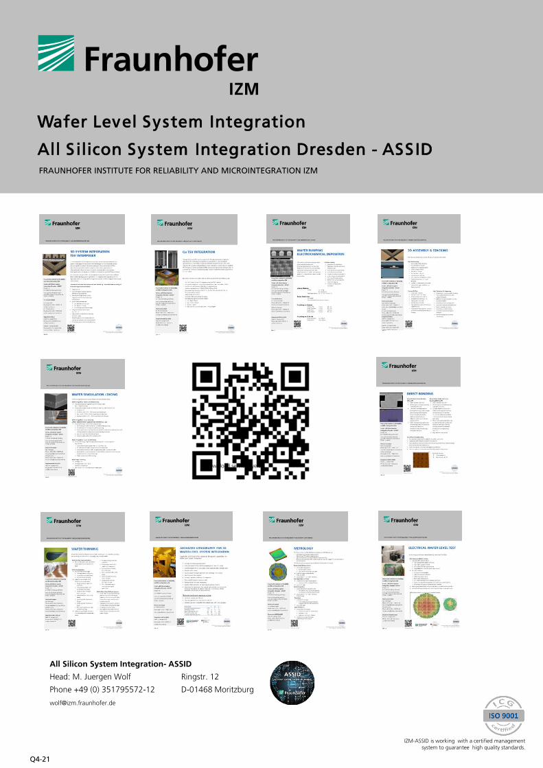
Wafer Level System Integration
All S ilicon System Integration Dresden - ASSID
All Silicon System Integration- ASSID
Head: M. Juergen Wolf Ringstr. 12
Phone +49 (0) 351795572-12 D-01468 Moritzburg
FRAUNHOFER INSTITUTE FOR RELIABILITY AND MICROINTEGRATION IZM
Q4-21
FRAUNHOFER INSTITUTE FOR RELIABILITY AND MICROINTEGRATION IZM
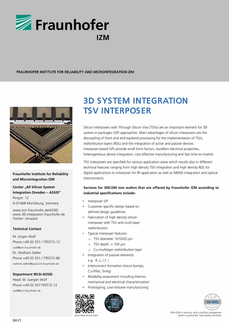
3D SYSTEM INTEGRATIONTSV INTERPOSER
Silicon interposers with Through Silicon Vias (TSVs) are an important element for 3D
system-in-packages (SiP) approaches. Main advantages of silicon interposers are the
decoupling of front end and backend processing for the implementation of TSVs,
redistribution layers (RDL) and the integration of active and passive devices.
Interposer-based SiPs provide small form factors, excellent electrical properties,
heterogeneous device integration, cost effective manufacturing and fast time-to-market.
TSV interposers are specified for various application areas which results also in different
technical features ranging from high density TSV integration and high density RDL for
digital applications to interposer for RF application as well as MEMS integration and optical
interconnects.
Services for 300/200 mm wafers that are offered by Fraunhofer IZM according to
industrial specifications include:
• Interposer SiP
• Customer specific design based on
defined design guidelines
• Fabrication of high density silicon
interposer with TSV and multi-layer
redistribution
• Typical interposer features:
o TSV diameter: 5/10/20 µm
o TSV depth: > 100 µm
o Cu-multilayer redistribution layer
• Integration of passive elements
e.g. R, L, ( C )
• Interconnect formation (micro bumps,
Cu-Pillar, SnAg)
• Reliability assessment including thermo-
mechanical and electrical characterization
• Prototyping, Low-Volume manufacturing
Fraunhofer Institute for Reliability
and Microintegration IZM
Center „All Silicon System
Integration Dresden – ASSID“
Ringstr. 12
D-01468 Moritzburg, Germany
www.izm.fraunhofer.de/ASSIDwww.3D-integration.fraunhofer.deTwitter: izmassid
Steller
Wolf
Department WLSI
Head: M. Juergen Wolf
Phone +49 (0) 351795572-12
Head: Oswin Ehrmann
Phone +49 (0) 30 / 464 03-124
IZM-ASSID is working with a certified management
system to guarantee high quality standards.Download service flyers
Fraunhofer Institute for Reliability
and Microintegration IZM
Center „All Silicon System
Integration Dresden – ASSID“
Ringstr. 12
D-01468 Moritzburg, Germany
www.izm.fraunhofer.de/ASSIDwww.3D-integration.fraunhofer.deTwitter: izmassid
Technical Contact
M. Jürgen Wolf
Phone +49 (0) 351 / 795572-12
Dr. Wolfram Steller
Phone +49 (0) 351 / 795572-86
Department WLSI-ASSID
Head: M. Juergen Wolf
Phone +49 (0) 351795572-12
FRAUNHOFER INSTITUTE FOR RELIABILITY AND MICROINTEGRATION IZM
Q4-21
FRAUNHOFER INSTITUTE FOR RELIABILITY AND MICROINTEGRATION IZM
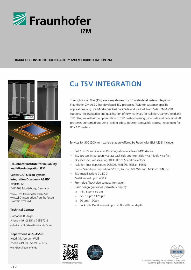
Cu TSV INTEGRATION
Through Silicon Vias (TSV) are a key element for 3D wafer-level system integration.
Fraunhofer IZM-ASSID has developed TSV processes (POR) for customer-specific
applications, e. g. Via Middle, Via Last Back Side and Via Last Front Side. IZM-ASSID
supports the evaluation and qualification of new materials for isolation, barrier / seed and
TSV filling as well as the optimization of TSV post-processing (front side and back side). All
processes are carried out using leading-edge, industry-compatible process equipment for
8” / 12” wafers.
Services for 300 (200) mm wafers that are offered by Fraunhofer IZM-ASSID include:
• Full Cu-TSV and Cu liner TSV integration in active CMOS device
• TSV process integration: via-last back side and front side / via-middle / via first
• Dry etch incl. wet cleaning: DRIE, RIE of Si and Dielectrics
• Isolation liner deposition: SATEOS, PETEOS, PESilan, PESiN
• Barrier/seed-layer deposition PVD: Ti, Ta, Cu, TiN, WTi and MOCVD: TiN, Co
• TSV metallization: Cu-ECD
• Metal anneal up to 400°C
• Front side / back side contact formation
• Basic design guidelines (diameter / depth):
o min. 5 μm / 50 μm
o typ. 10 μm / 120 μm
o 20 μm / 120μm
o Back side TSV (Cu-liner) up to 250 – 700 μm depth
Fraunhofer Institute for Reliability
and Microintegration IZM
Center „All Silicon System
Integration Dresden – ASSID“
Ringstr. 12
D-01468 Moritzburg, Germany
www.izm.fraunhofer.de/ASSIDwww.3D-integration.fraunhofer.deTwitter: izmassid
Technical Contact
Catharina Rudolph
Phone +49 (0) 351 / 795572-61
Department WLSI-ASSID
Head: M. Juergen Wolf
Phone +49 (0) 351795572-12
IZM-ASSID is working with a certified management
system to guarantee high quality standards.Download service flyers
FRAUNHOFER INSTITUTE FOR RELIABILITY AND MICROINTEGRATION IZM
Q4-21
FRAUNHOFER INSTITUTE FOR RELIABILITY AND MICROINTEGRATION IZM
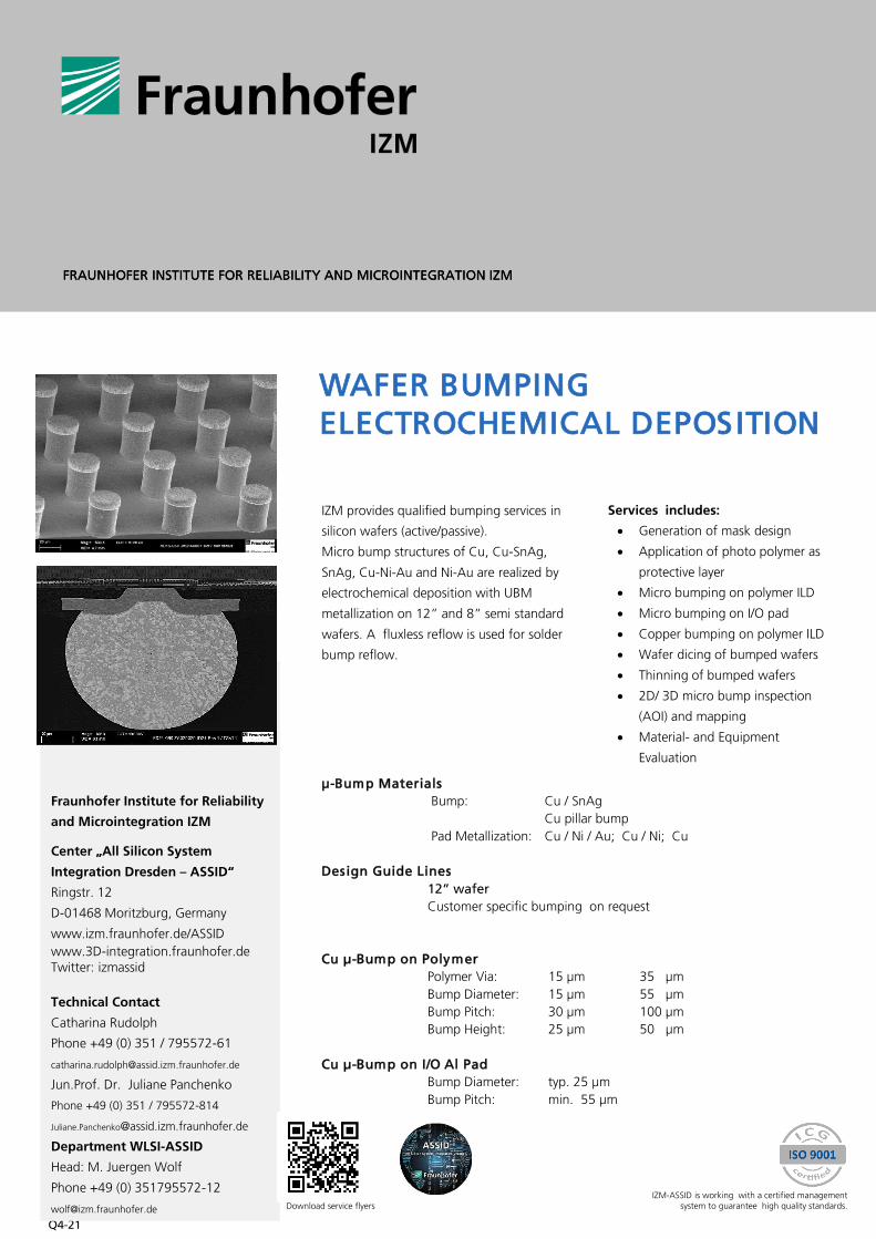
WAFER BUMPING ELECTROCHEMICAL DEPOSITION
IZM provides qualified bumping services in
silicon wafers (active/passive).
Micro bump structures of Cu, Cu-SnAg,
SnAg, Cu-Ni-Au and Ni-Au are realized by
electrochemical deposition with UBM
metallization on 12” and 8” semi standard
wafers. A fluxless reflow is used for solder
bump reflow.
µ-Bump Materials
Bump: Cu / SnAg
Cu pillar bump
Pad Metallization: Cu / Ni / Au; Cu / Ni; Cu
Design Guide Lines
12” wafer
Customer specific bumping on request
Cu µ-Bump on Polymer
Polymer Via: 15 µm 35 µm
Bump Diameter: 15 µm 55 µm
Bump Pitch: 30 µm 100 µm
Bump Height: 25 µm 50 µm
Cu µ-Bump on I/O Al Pad
Bump Diameter: typ. 25 µm
Bump Pitch: min. 55 µm
Fraunhofer Institute for Reliability
and Microintegration IZM
Center „All Silicon System
Integration Dresden – ASSID“
Ringstr. 12
D-01468 Moritzburg, Germany
www.izm.fraunhofer.de/ASSID
www.3D-integration.fraunhofer.deTwitter: izmassid
Technical Contact
Catharina Rudolph
Phone +49 (0) 351 / 795572-61
Jun.Prof. Dr. Juliane Panchenko
Phone +49 (0) 351 / 795572-814
Department WLSI-ASSID
Head: M. Juergen Wolf
Phone +49 (0) 351795572-12
Services includes:
Generation of mask design
Application of photo polymer as
protective layer
Micro bumping on polymer ILD
Micro bumping on I/O pad
Copper bumping on polymer ILD
Wafer dicing of bumped wafers
Thinning of bumped wafers
2D/ 3D micro bump inspection
(AOI) and mapping
Material- and Equipment
Evaluation
IZM-ASSID is working with a certified management
system to guarantee high quality standards.Download service flyers
FRAUNHOFER INSTITUTE FOR RELIABILITY AND MICROINTEGRATION IZM
Q4-21
FRAUNHOFER INSTITUTE FOR RELIABILITY AND MICROINTEGRATION IZM
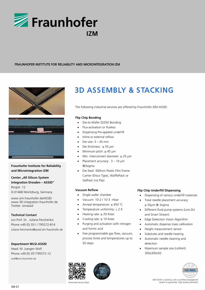
3D ASSEMBLY & STACKING
Flip Chip Bonding
Die-to-Wafer (D2W) Bonding
Flux-activation or fluxless
Dispensing Pre-applied underfill
Inline or external reflow
Die size: 3 – 30 mm
Die thickness: ≥ 50 µm
Minimum pitch: ≥ 45 µm
Min. interconnect diameter: ≥ 25 µm
Placement accuracy: 3 – 10 µm
@3sigma
Die feed: 300mm Plastic Film Frame
Carrier (Disco Type), WafflePack or
GelPack (no Flip)
Vacuum Reflow
Single wafer chamber
Vacuum: 10-2 / 10-3 mbar
Anneal temperature: ≤ 450 °C
Temperature uniformity: ± 2 K
Heating rate: ≥ 20 K/sec
Cooling rate: ≤ 10 K/sec
Purging and activation with nitrogen
and formic acid
free programmable gas flow, vacuum,
process times and temperatures up to
50 steps
The following industrial services are offered by Fraunhofer IZM-ASSID:
Fraunhofer Institute for Reliability
and Microintegration IZM
Center „All Silicon System
Integration Dresden – ASSID“
Ringstr. 12
D-01468 Moritzburg, Germany
www.izm.fraunhofer.de/ASSIDwww.3D-integration.fraunhofer.deTwitter: izmassid
Technical Contact
Jun.Prof. Dr. Juliane Panchenko
Phone +49 (0) 351 / 795572-814
Department WLSI-ASSID
Head: M. Juergen Wolf
Phone +49 (0) 351795572-12
IZM-ASSID is working with a certified management
system to guarantee high quality standards.Download service flyers
Flip Chip Underfill Dispensing
Dispensing of various underfill materials
Total needle placement accuracy:
≥ 50µm @ 3sigma
Different fluid pump systems (Line DU
and Smart Stream)
Edge Detection Vision Algorithm
Automatic dispense mass calibration
Height measurement sensor
Substrate and needle heating
Automatic needle cleaning and
detection
Maximum sample size (LxWxH):
300x300x50
FRAUNHOFER INSTITUTE FOR RELIABILITY AND MICROINTEGRATION IZM
Q4-21
FRAUNHOFER INSTITUTE FOR RELIABILITY AND MICROINTEGRATION IZM
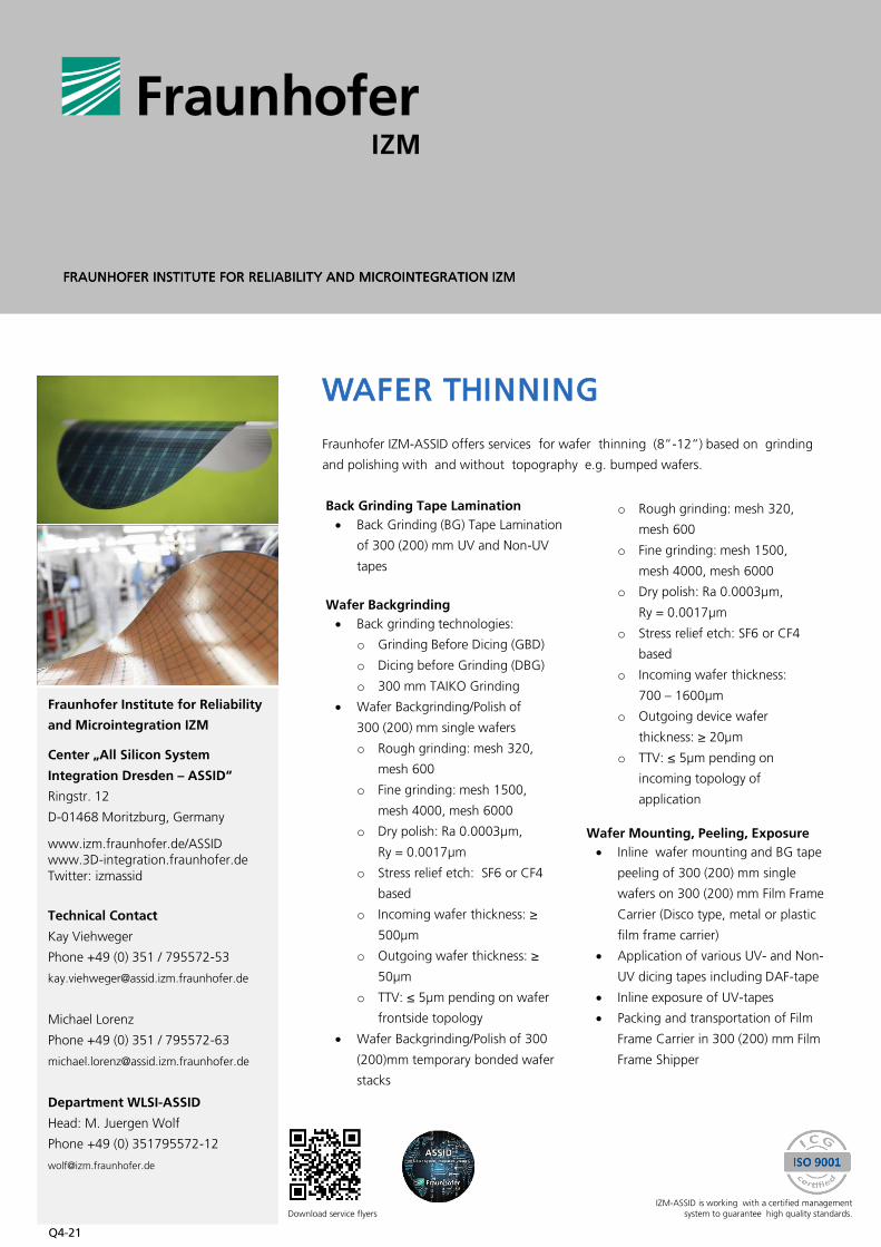
WAFER THINNING
Fraunhofer IZM-ASSID offers services for wafer thinning (8”-12”) based on grinding
and polishing with and without topography e.g. bumped wafers.
IZM-ASSID is working with a certified management
system to guarantee high quality standards.Download service flyers
Fraunhofer Institute for Reliability
and Microintegration IZM
Center „All Silicon System
Integration Dresden – ASSID“
Ringstr. 12
D-01468 Moritzburg, Germany
www.izm.fraunhofer.de/ASSIDwww.3D-integration.fraunhofer.deTwitter: izmassid
Technical Contact
Kay Viehweger
Phone +49 (0) 351 / 795572-53
Michael Lorenz
Phone +49 (0) 351 / 795572-63
Department WLSI-ASSID
Head: M. Juergen Wolf
Phone +49 (0) 351795572-12
Back Grinding Tape Lamination
Back Grinding (BG) Tape Lamination
of 300 (200) mm UV and Non-UV
tapes
Wafer Backgrinding
Back grinding technologies:
o Grinding Before Dicing (GBD)
o Dicing before Grinding (DBG)
o 300 mm TAIKO Grinding
Wafer Backgrinding/Polish of
300 (200) mm single wafers
o Rough grinding: mesh 320,
mesh 600
o Fine grinding: mesh 1500,
mesh 4000, mesh 6000
o Dry polish: Ra 0.0003µm,
Ry = 0.0017µm
o Stress relief etch: SF6 or CF4
based
o Incoming wafer thickness: ≥
500µm
o Outgoing wafer thickness: ≥
50µm
o TTV: ≤ 5µm pending on wafer
frontside topology
Wafer Backgrinding/Polish of 300
(200)mm temporary bonded wafer
stacks
o Rough grinding: mesh 320,
mesh 600
o Fine grinding: mesh 1500,
mesh 4000, mesh 6000
o Dry polish: Ra 0.0003µm,
Ry = 0.0017µm
o Stress relief etch: SF6 or CF4
based
o Incoming wafer thickness:
700 – 1600µm
o Outgoing device wafer
thickness: ≥ 20µm
o TTV: ≤ 5µm pending on
incoming topology of
application
Wafer Mounting, Peeling, Exposure
Inline wafer mounting and BG tape
peeling of 300 (200) mm single
wafers on 300 (200) mm Film Frame
Carrier (Disco type, metal or plastic
film frame carrier)
Application of various UV- and Non-
UV dicing tapes including DAF-tape
Inline exposure of UV-tapes
Packing and transportation of Film
Frame Carrier in 300 (200) mm Film
Frame Shipper
FRAUNHOFER INSTITUTE FOR RELIABILITY AND MICROINTEGRATION IZM
Q4-21
Wafer Singulation - Mechanical Blade Dicing
Mechanical blade dicing of 300 (200) mm single wafer
(50 – 775µm thickness)
Dicing technologies: Single Cut (Dual Cut), Step Cut, Half Cut (Dual Cut)
o Grid type: SD
o Grid size: mesh 1700 – 3500 (pending on blade type)
o Kerf width: 0,025 – 0,06mm (pending on blade types)
o Exposure height: 0,38 – 1,24mm (pending on blade type)
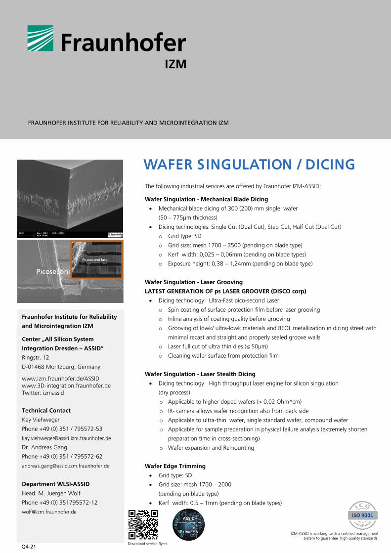
Wafer Singulation - Laser Grooving
LATEST GENERATION OF ps LASER GROOVER (DISCO corp)
Dicing technology: Ultra-Fast pico-second Laser
o Spin coating of surface protection film before laser grooving
o Inline analysis of coating quality before grooving
o Grooving of lowk/ ultra-lowk materials and BEOL metallization in dicing street with
minimal recast and straight and properly sealed groove walls
o Laser full cut of ultra thin dies (≤ 50µm)
o Cleaning wafer surface from protection film
Wafer Singulation - Laser Stealth Dicing
Dicing technology: High throughput laser engine for silicon singulation
(dry process)
o Applicable to higher doped wafers (> 0,02 Ohm*cm)
o IR- camera allows wafer recognition also from back side
o Applicable to ultra-thin wafer, single standard wafer, compound wafer
o Applicable for sample preparation in physical failure analysis (extremely shorten
preparation time in cross-sectioning)
o Wafer expansion and Remounting
Wafer Edge Trimming
Grid type: SD
Grid size: mesh 1700 – 2000
(pending on blade type)
Kerf width: 0,5 – 1mm (pending on blade types)
WAFER SINGULATION / DICING
Fraunhofer Institute for Reliability
and Microintegration IZM
Center „All Silicon System
Integration Dresden – ASSID“
Ringstr. 12
D-01468 Moritzburg, Germany
www.izm.fraunhofer.de/ASSIDwww.3D-integration.fraunhofer.deTwitter: izmassid
Technical Contact
Dr. Juergen Grafe
Phone +49 (0) 351 / 795572-60
Viehweger
Department WLSI
Head: M. Juergen Wolf
Phone +49 (0) 351795572-12
Head: Oswin Ehrmann
Phone +49 (0) 30 / 464 03-124
The following industrial services are offered by Fraunhofer IZM-ASSID:
IZM-ASSID is working with a certified management
system to guarantee high quality standards.
Download service flyers
Fraunhofer Institute for Reliability
and Microintegration IZM
Center „All Silicon System
Integration Dresden – ASSID“
Ringstr. 12
D-01468 Moritzburg, Germany
www.izm.fraunhofer.de/ASSIDwww.3D-integration.fraunhofer.deTwitter: izmassid
Technical Contact
Kay Viehweger
Phone +49 (0) 351 / 795572-53
Dr. Andreas Gang
Phone +49 (0) 351 / 795572-62
Department WLSI-ASSID
Head: M. Juergen Wolf
Phone +49 (0) 351795572-12
© GLOBALFOUNDRIES
FRAUNHOFER INSTITUTE FOR RELIABILITY AND MICROINTEGRATION IZM
Q4-21
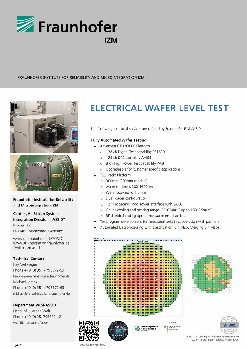
Fully Automated Wafer Testing
Advantest CTH 93000 Platform
o 128 ch Digital Test capability PS1600
o 128 ch DPS capability AVI64
o 8 ch High Power Test capability PVI8
o Upgradeable for customer specific applications
TEL Precio Platform
o 300mm (200mm capable)
o wafer thickness 300-1600µm
o Wafer bow up to 1.5mm
o Dual loader configuration
o 12” Probecard Pogo Tower Interface with SACC
o Chuck cooling and heating range -55°C/-40°C up to 150°C/200°C
o RF shielded and lightproof measurement chamber
Testprogram development for functional tests in cooperation with partners
Automated Dataprocessing with classification, Bin Map, Merging Bin Maps
ELECTRICAL WAFER LEVEL TEST
Fraunhofer Institute for Reliability
and Microintegration IZM
Center „All Silicon System
Integration Dresden – ASSID“
Ringstr. 12
D-01468 Moritzburg, Germany
www.izm.fraunhofer.de/ASSIDwww.3D-integration.fraunhofer.deTwitter: izmassid
Technical Contact
Dr. Juergen Grafe
Phone +49 (0) 351 / 795572-60
Viehweger
Department WLSI
Head: M. Juergen Wolf
Phone +49 (0) 351795572-12
Head: Oswin Ehrmann
Phone +49 (0) 30 / 464 03-124
The following industrial services are offered by Fraunhofer IZM-ASSID:
IZM-ASSID is working with a certified management
system to guarantee high quality standards.
Fraunhofer Institute for Reliability
and Microintegration IZM
Center „All Silicon System
Integration Dresden – ASSID“
Ringstr. 12
D-01468 Moritzburg, Germany
www.izm.fraunhofer.de/ASSIDwww.3D-integration.fraunhofer.deTwitter: izmassid
Technical Contact
Kay Viehweger
Phone +49 (0) 351 / 795572-53
Michael Lorenz
Phone +49 (0) 351 / 795572-63
Department WLSI-ASSID
Head: M. Juergen Wolf
Phone +49 (0) 351795572-12
Download service flyers
__ __ __ __ __ __ 4 4 4 4 4 __ __ __ __ __ __
__ __ __ __ 4 4 4 4 4 4 4 4 0 __ __ __ __
__ __ __ 4 4 4 4 4 4 4 4 4 3 4 __ __ __
__ __ 4 4 4 4 4 4 3 3 4 4 4 3 4 __ __
__ __ 4 4 4 4 4 4 3 4 4 4 4 4 4 __ __
__ 4 4 4 4 3 3 3 3 3 4 4 4 4 4 0 __
__ 4 4 4 4 4 3 3 3 3 4 4 4 4 3 4 __
__ 4 4 4 4 3 4 3 3 3 2 3 4 4 4 3 4
4 4 4 4 4 3 3 3 3 3 4 3 4 4 4 3 4
4 4 4 4 4 2 3 3 3 3 4 3 4 3 4 4 4
4 4 4 4 4 4 4 3 3 3 3 3 4 4 4 0 4
4 4 4 4 4 4 3 4 3 3 4 3 4 4 4 4 4
4 3 4 4 4 4 4 3 3 4 4 4 4 4 4 4 0
__ 4 4 4 4 4 4 3 4 4 4 4 4 3 4 4 __
__ 4 4 4 4 4 4 4 4 3 4 0 4 0 3 3 __
__ 4 4 4 4 4 4 4 4 4 4 4 4 3 4 0 __
__ __ 4 4 4 4 4 4 4 4 4 4 4 4 4 __ __
__ __ 4 4 4 4 4 4 4 4 4 4 4 4 0 __ __
__ __ __ 4 4 4 4 3 4 3 4 3 4 4 __ __ __
__ __ __ __ 4 4 0 4 4 4 4 0 4 __ __ __ __
__ __ __ __ __ __ 4 4 4 4 4 __ __ __ __ __ __
FRAUNHOFER INSTITUTE FOR RELIABILITY AND MICROINTEGRATION IZM
Q4-21
FRAUNHOFER INSTITUTE FOR RELIABILITY AND MICROINTEGRATION IZM
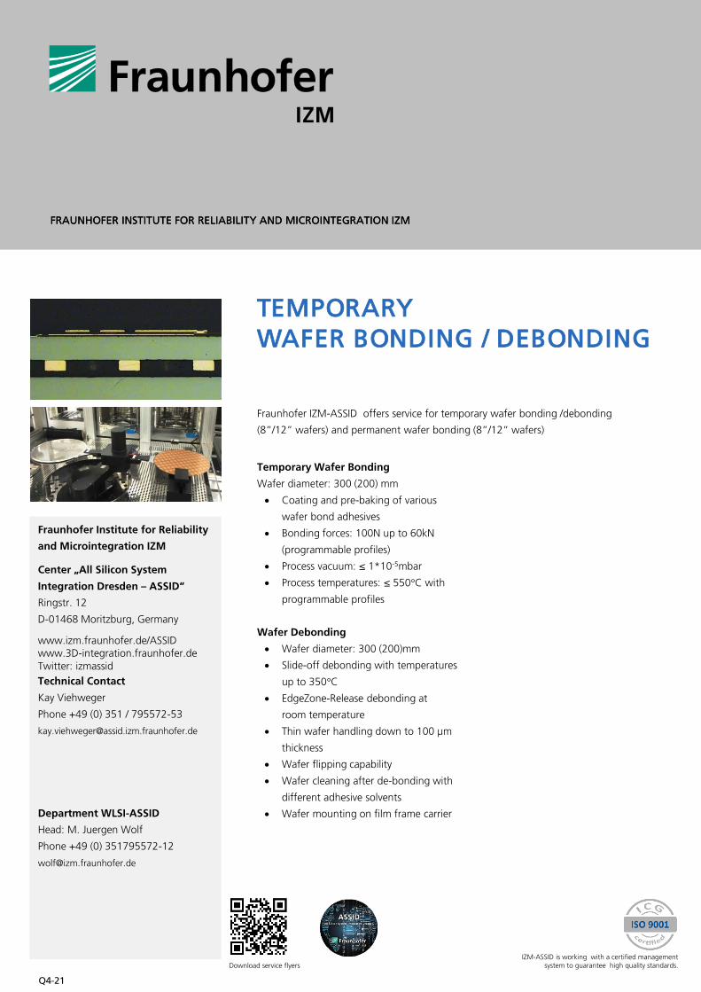
TEMPORARY WAFER BONDING / DEBONDING
Temporary Wafer Bonding
Wafer diameter: 300 (200) mm
Coating and pre-baking of various
wafer bond adhesives
Bonding forces: 100N up to 60kN
(programmable profiles)
Process vacuum: ≤ 1*10-5mbar
Process temperatures: ≤ 550°C with
programmable profiles
Wafer Debonding
Wafer diameter: 300 (200)mm
Slide-off debonding with temperatures
up to 350°C
EdgeZone-Release debonding at
room temperature
Thin wafer handling down to 100 µm
thickness
Wafer flipping capability
Wafer cleaning after de-bonding with
different adhesive solvents
Wafer mounting on film frame carrier
Fraunhofer IZM-ASSID offers service for temporary wafer bonding /debonding
(8”/12” wafers) and permanent wafer bonding (8”/12” wafers)
Fraunhofer Institute for Reliability
and Microintegration IZM
Center „All Silicon System
Integration Dresden – ASSID“
Ringstr. 12
D-01468 Moritzburg, Germany
www.izm.fraunhofer.de/ASSIDwww.3D-integration.fraunhofer.deTwitter: izmassid
Technical Contact
Kay Viehweger
Phone +49 (0) 351 / 795572-53
Department WLSI-ASSID
Head: M. Juergen Wolf
Phone +49 (0) 351795572-12
IZM-ASSID is working with a certified management
system to guarantee high quality standards.Download service flyers
FRAUNHOFER INSTITUTE FOR RELIABILITY AND MICROINTEGRATION IZM
Q4-21
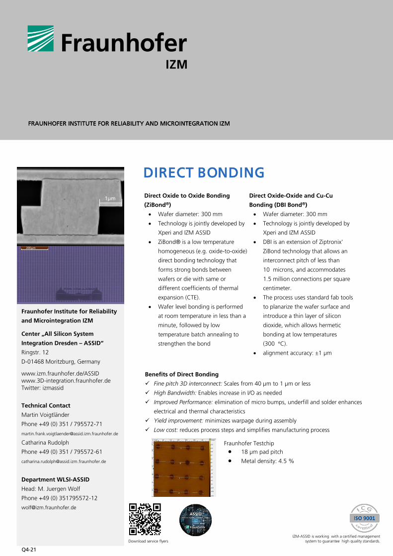
1µm
FRAUNHOFER INSTITUTE FOR RELIABILITY AND MICROINTEGRATION IZM
DIRECT BONDING
Fraunhofer Institute for Reliability
and Microintegration IZM
Center „All Silicon System
Integration Dresden – ASSID“
Ringstr. 12
D-01468 Moritzburg, Germany
www.izm.fraunhofer.de/ASSIDwww.3D-integration.fraunhofer.deTwitter: izmassid
Technical Contact
Martin Voigtländer
Phone +49 (0) 351 / 795572-71
Catharina Rudolph
Phone +49 (0) 351 / 795572-61
Department WLSI-ASSID
Head: M. Juergen Wolf
Phone +49 (0) 351795572-12
Benefits of Direct Bonding
Fine pitch 3D interconnect: Scales from 40 µm to 1 µm or less
High Bandwidth: Enables increase in I/O as needed
Improved Performance: elimination of micro bumps, underfill and solder enhances
electrical and thermal characteristics
Yield improvement: minimizes warpage during assembly
Low cost: reduces process steps and simplifies manufacturing process
Fraunhofer Testchip
18 µm pad pitch
Metal density: 4.5 %
200µm
Download service flyers
Direct Oxide to Oxide Bonding
(ZiBond®)
Wafer diameter: 300 mm
Technology is jointly developed by
Xperi and IZM ASSID
ZiBond® is a low temperature
homogeneous (e.g. oxide-to-oxide)
direct bonding technology that
forms strong bonds between
wafers or die with same or
different coefficients of thermal
expansion (CTE).
Wafer level bonding is performed
at room temperature in less than a
minute, followed by low
temperature batch annealing to
strengthen the bond
Direct Oxide-Oxide and Cu-Cu
Bonding (DBI Bond®)
Wafer diameter: 300 mm
Technology is jointly developed by
Xperi and IZM ASSID
DBI is an extension of Ziptronix'
ZiBond technology that allows an
interconnect pitch of less than
10 microns, and accommodates
1.5 million connections per square
centimeter.
The process uses standard fab tools
to planarize the wafer surface and
introduce a thin layer of silicon
dioxide, which allows hermetic
bonding at low temperatures
(300 °C).
alignment accuracy: ±1 µm
1µm
IZM-ASSID is working with a certified management
system to guarantee high quality standards.
FRAUNHOFER INSTITUTE FOR RELIABILITY AND MICROINTEGRATION IZM
Q4-21
FRAUNHOFER INSTITUTE FOR RELIABILITY AND MICROINTEGRATION IZM
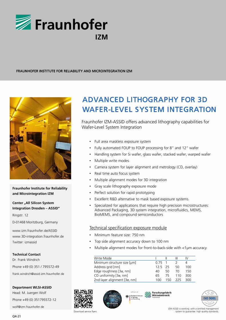
ADVANCED LITHOGRAPHY FOR 3D
WAFER-LEVEL SYSTEM INTEGRATION
Fraunhofer IZM-ASSID offers advanced lithography capabilities for Wafer-Level System Integration
Fraunhofer Institute for Reliability
and Microintegration IZM
Center „All Silicon System
Integration Dresden – ASSID“
Ringstr. 12
D-01468 Moritzburg, Germany
www.izm.fraunhofer.de/ASSID
www.3D-integration.fraunhofer.de
Twitter: izmassid
Technical Contact
Dr. Frank Windrich
Phone +49 (0) 351 / 795572-49
Department WLSI-ASSID
Head: M. Juergen Wolf
Phone +49 (0) 351795572-12
Download service flyers
Write Mode I II III IV
Minimum structure size [µm] 0.75 1 2 4
Address grid [nm] 12.5 25 50 100Edge roughness [3σ, nm] 40 50 70 150CD uniformity [3σ, nm] 65 75 110 300
2nd layer alignment [3σ, nm] 100 150 225 300
• Full area maskless exposure system
• Fully automated FOUP to FOUP processing for 8” and 12” wafer
• Handling system for Si wafer, glass wafer, stacked wafer, warped wafer
• Multiple write modes
• Camera system for layer alignment and metrology (CD, overlay)
• Real time auto focus system
• Multiple alignment modes for 3D integration
• Gray scale lithography exposure mode
• Perfect solution for rapid prototyping
• Excellent R&D alternative to mask based exposure systems
• Specialized for applications that require high precision microstructures: Advanced Packaging, 3D system integration, microfluidics, MEMS, BioMEMS, and compound semiconductors
Technical specification exposure module
• Minimum feature size: 750 nm
• Top side alignment accuracy down to 100 nm
• Multiple alignment modes for front-to-back-side with <1µm accuracy
IZM-ASSID is working with a certified management
system to guarantee high quality standards.
FRAUNHOFER INSTITUTE FOR RELIABILITY AND MICROINTEGRATION IZM
Q4-21
FRAUNHOFER INSTITUTE FOR RELIABILITY AND MICROINTEGRATION IZM
METROLOGY
Bump Height Measurement
white light triangulation
o bump height 7-80 µm
o up to 25 million bumps per wafer
high throughput measurement (max. 15 wph)
automated 4’’ - 12’’ wafer handling
TSV-depth Measurement
interferometric depth measurement
o 1µm up to 300 (confocal: 700µm)
up to 12’’ wafer
Defect Inspection
automated defect inspection (AOI)
o min. defect size 1 µm-5 µm (depends on structure complexity and contrast)
automated 4’’ - 12’’ wafer handling & film frames
Topology
confocal microscopy
o 5 nm surface topology @ mag 20x (opaque materials: higher accuracy)
up to 12’’ wafer
Layer Thickness
ellipsometry (thin layers):
o 5-2000 nm Oxid / 5-150 nm Nitrid
o polymer <5 µm
o layer stack with up to 3 layers
interferometric layer thickness measurement (thick layers):
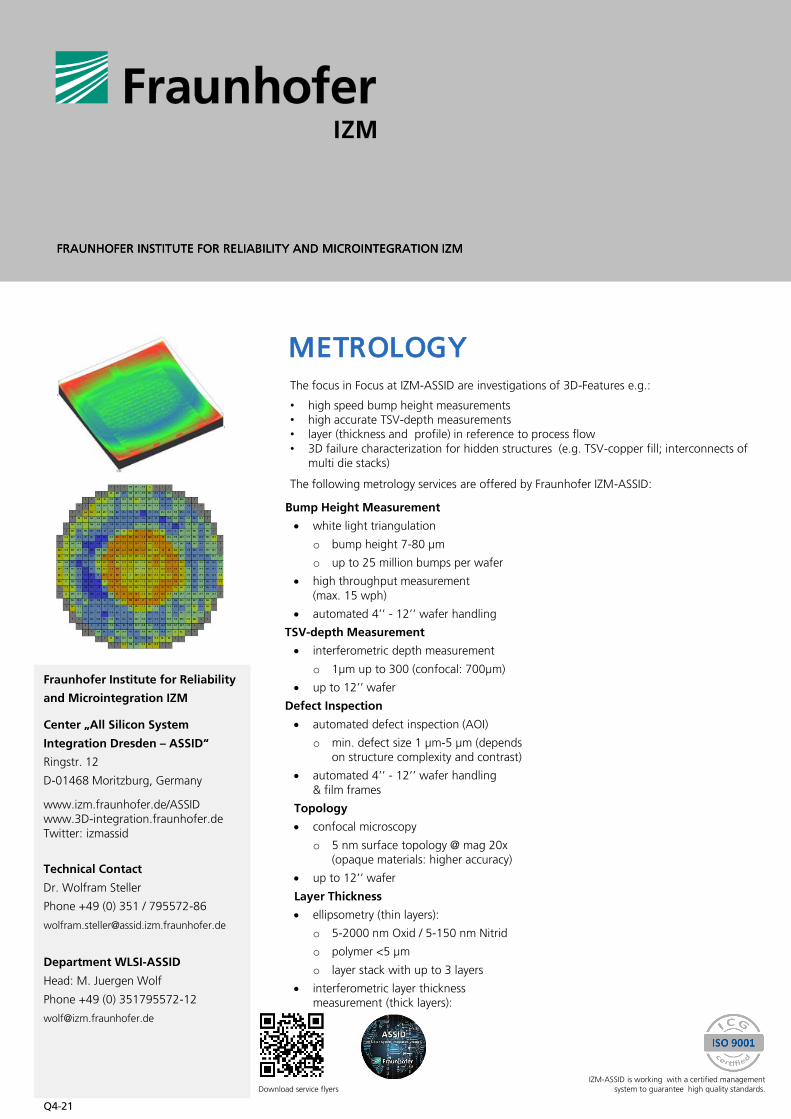
The focus in Focus at IZM-ASSID are investigations of 3D-Features e.g.:
• high speed bump height measurements• high accurate TSV-depth measurements• layer (thickness and profile) in reference to process flow• 3D failure characterization for hidden structures (e.g. TSV-copper fill; interconnects of
multi die stacks)
The following metrology services are offered by Fraunhofer IZM-ASSID:
Fraunhofer Institute for Reliability
and Microintegration IZM
Center „All Silicon System
Integration Dresden – ASSID“
Ringstr. 12
D-01468 Moritzburg, Germany
www.izm.fraunhofer.de/ASSIDwww.3D-integration.fraunhofer.deTwitter: izmassid
Technical Contact
Dr. Wolfram Steller
Phone +49 (0) 351 / 795572-86
Department WLSI-ASSID
Head: M. Juergen Wolf
Phone +49 (0) 351795572-12
IZM-ASSID is working with a certified management
system to guarantee high quality standards.Download service flyers
FRAUNHOFER INSTITUTE FOR RELIABILITY AND MICROINTEGRATION IZM
Q4-21
FRAUNHOFER INSTITUTE FOR RELIABILITY AND MICROINTEGRATION IZM
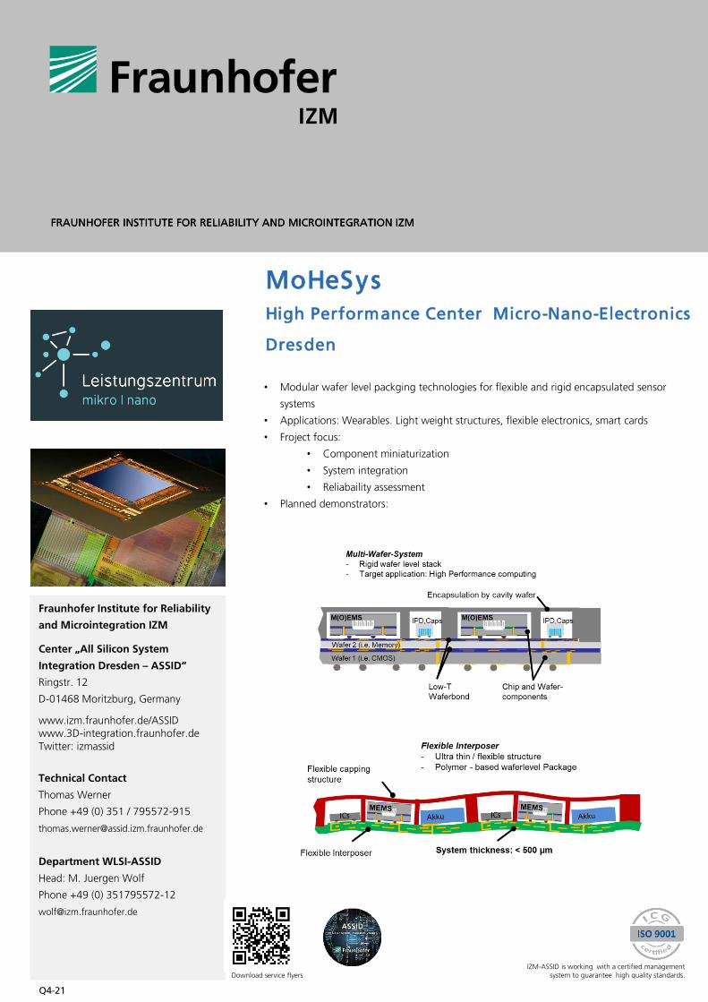
MoHeSysHigh Performance Center Micro-Nano-Electronics
Dresden
• Modular wafer level packging technologies for flexible and rigid encapsulated sensor
systems
• Applications: Wearables. Light weight structures, flexible electronics, smart cards
• Froject focus:
• Component miniaturization
• System integration
• Reliabaility assessment
• Planned demonstrators:
Fraunhofer Institute for Reliability
and Microintegration IZM
Center „All Silicon System
Integration Dresden – ASSID“
Ringstr. 12
D-01468 Moritzburg, Germany
www.izm.fraunhofer.de/ASSIDwww.3D-integration.fraunhofer.deTwitter: izmassid
Technical Contact
Thomas Werner
Phone +49 (0) 351 / 795572-915
Department WLSI-ASSID
Head: M. Juergen Wolf
Phone +49 (0) 351795572-12
IZM-ASSID is working with a certified management
system to guarantee high quality standards.Download service flyers