Wafer Fabrication Part II - NECTECtmec.nectec.or.th/.../research/ic_fabrication_en.pdf · 4 Wafer...
78
Wafer Fabrication Part II
Transcript of Wafer Fabrication Part II - NECTECtmec.nectec.or.th/.../research/ic_fabrication_en.pdf · 4 Wafer...

Wa fe r F a b ric a tio n P a rt II

22
Introduction to Wafer Fabrication
• Introduction to TMEC• History from Edison’s Light Bulb to Pentium 4• Semiconductor Materials • Wafer Preparation• Wafer Fabrication Processes• Thin Film Deposition Process• Patterning Process• Etching Process• Doping Process• Contamination

33
Microelectronics Fabrication
Lithography
Etching
Doping
Thin Film Deposition

44
Wafer Fabrication Processes
CMOS Process Bipolar Process
BiCMOS Process
Technologie 0.25µm BiCMOS SiGe,Philips

55
CMOS Process Flow
p-type Silicon Substrate
1. Starting wafer2. n-well3. Active4. Gate5. Junction6. ILD7. Contacts and metal 18. Vias and metal 29. Passivation

66
Wafer
p-type Cz wafer
p-type

77
Process flow
p-type Silicon Substrate
1. Starting wafer2. n-well3. Active4. Gate5. Junction6. ILD7. Contacts and metal 18. Vias and metal 29. Passivation

88
Initial oxidation: O2/H2 (Thickness: 420 nm)
p-type
n-well
SiO2

99
n-well
Photolithography : NWELL
p-type
Photoresist (PR)

1010
n-well
Dry etch oxide
p-type
1111
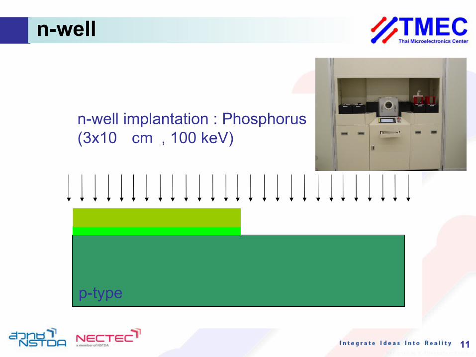
n-well
n-well implantation : Phosphorus (3x1012 cm-3, 100 keV)
p-type

1212
Resist strip
p-type
n-well

1313
n-well drive : Anneal : N2
Differential Oxidation : O2/H2 Anneal : N2
p-type
n-well
n-well

1414
Process flow
p-type Silicon Substrate
1. Starting wafer2. n-well3. Active4. Gate5. Junction6. ILD7. Contacts and metal 18. Vias and metal 29. Passivation

1515
Active
Wet etch all oxide + Pad oxidation (20 nm)
p-type
n-well

1616
Deposition : Nitride (150 nm)
p-type
n-well
Active

1717
Photolithography : ACTIVE
p-type
n-well
Active

1818
Dry etch nitride
p-type
n-well
Active

1919
Resist strip
p-type
n-well
Active

2020
Photolithography : NFIELD
p-type
n-well
Active

2121
NField implantation : Boron (8x1013 cm-3, 60 keV)
p-type
n-well
Active

2222
Resist strip
p-type
n-well
Active
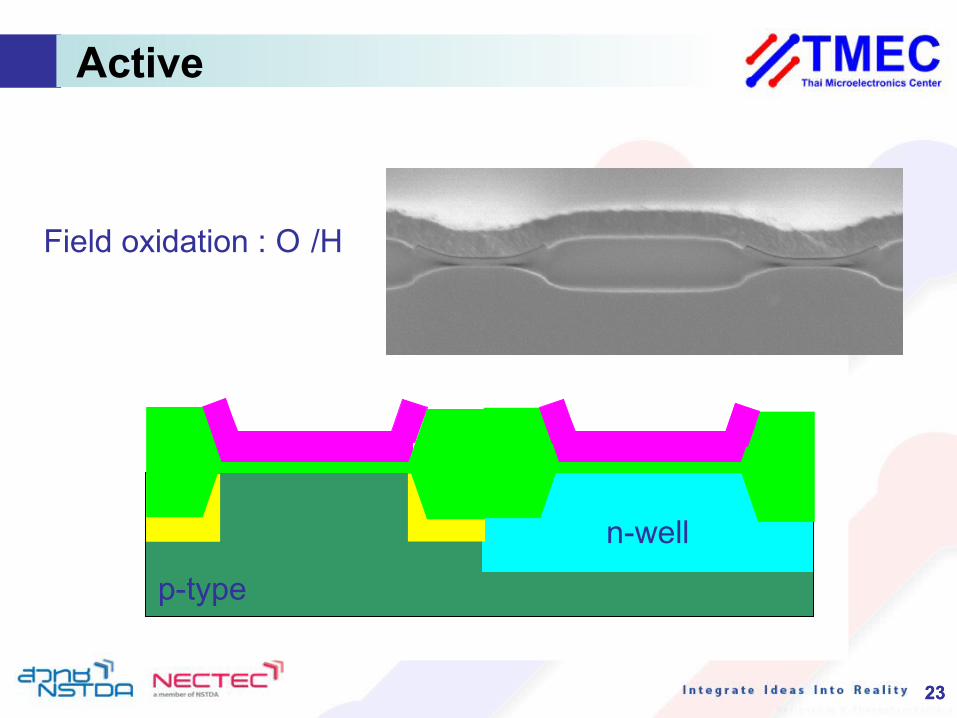
2323
Field oxidation : O2/H2
p-type
n-well
Active

2424
Active
Wet etch Nitride
p-type
n-well
Active

2525
Process flow
p-type Silicon Substrate
1. Starting wafer2. n-well3. Active4. Gate5. Junction6. ILD7. Contacts and metal 18. Vias and metal 29. Passivation

2626
Gate
Etch Pad oxide + WR oxidation : H2/O2 (50 nm)
p-type
n-well

2727
Photolithography : NFIELD
p-type
n-well
Gate

2828
APT Implantation : Boron (6.5x1011 cm-3, 110 keV)
p-type
n-well
Gate

2929
Resist strip
p-type
n-well
Gate

3030
Anneal : N2
p-type
n-well
Gate

3131
Etch WR oxide + Gate oxidation (25 nm)
p-type
n-well
Gate

3232
VTA implantation : Boron (8x1011 cm-3, 20 keV)
p-type
n-well
Gate

3333
Poly deposition
p-type
n-well
Gate

3434
TEOS deposition
p-type
n-well
Gate

3535
Poly implantation : Phosphorus (1.2x1016 cm-3, 50 keV)
p-type
n-well
Gate

3636
Anneal : N2
p-type
n-well
Gate

3737
Wet etch TEOS
p-type
n-well
Gate

3838
Photolithography : POLY
p-type
n-well
Gate

3939
Dry etch poly
p-type
n-well
Gate
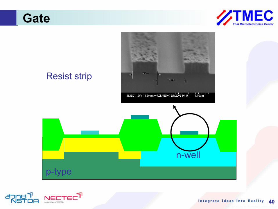
4040
Resist strip
p-type
n-well
Gate

4141
Process flow
p-type Silicon Substrate
1. Starting wafer2. n-well3. Active4. Gate5. Junction6. ILD7. Contacts and metal 18. Vias and metal 29. Passivation

4242
Junctions
Oxidation : O2
p-type
n-well

4343
Photolithography : NPLUS
p-type
n-well
Junctions
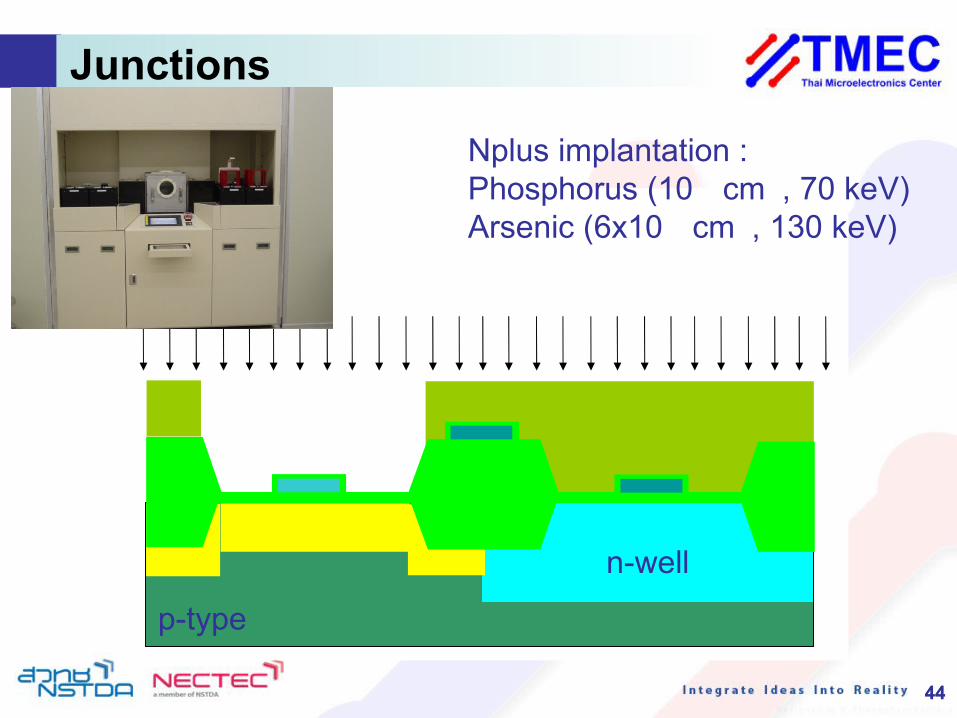
4444
Nplus implantation : Phosphorus (1014 cm-2, 70 keV)Arsenic (6x1015 cm-2, 130 keV)
p-type
n-well
Junctions

4545
Resist strip
p-type
n-well
Junctions

4646
Photolithography : PPLUS
p-type
n-well
Junctions

4747
Pplus implantation :Boron (5x1015 cm-2, 20 keV)
p-type
n-well
Junctions

4848
Resist strip
p-type
n-well
Junctions

4949
Coat front + Backside etch
p-type
n-well
Junctions

5050
Resist strip
p-type
n-well
Junctions
5151
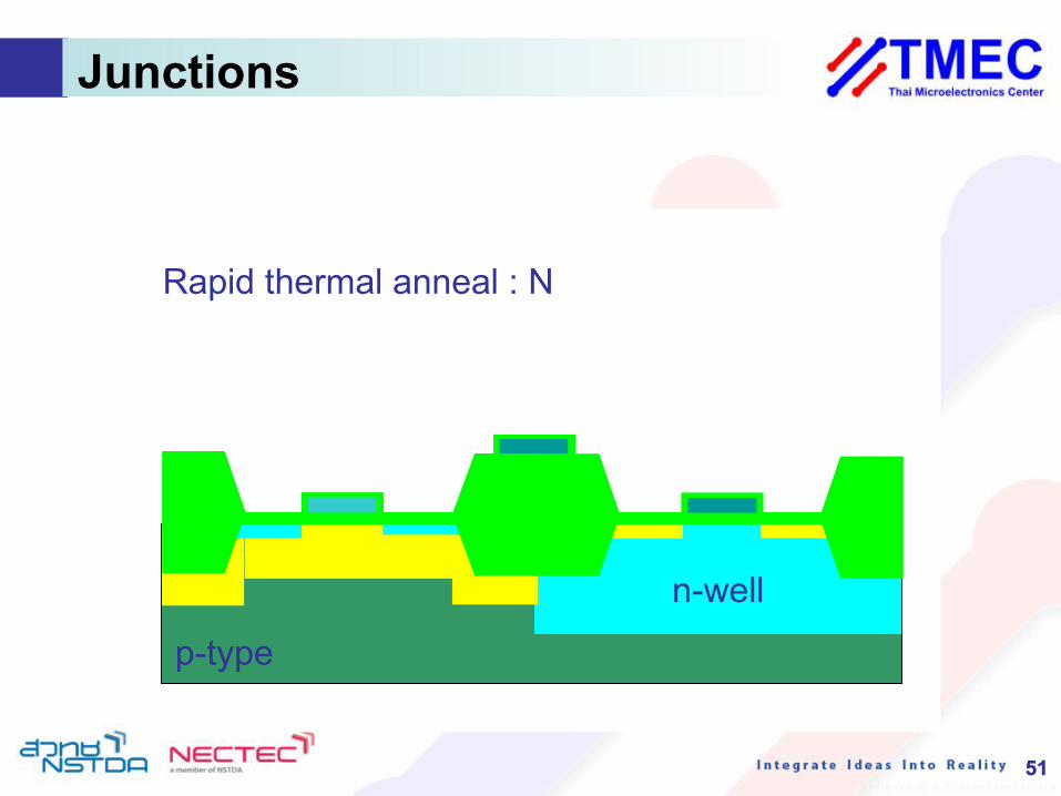
Rapid thermal anneal : N2
p-type
n-well
Junctions

5252
Process flow
p-type Silicon Substrate
1. Starting wafer2. n-well3. Active4. Gate5. Junction6. Interlayer Dielectric (ILD)7. Contacts and metal 18. Vias and metal 29. Passivation

5353
Interlayer Dielectric
TEOS deposition : UTEOS
p-type
n-well

5454
SOG coatSOG cureSOG coatSOG Cure
p-type
n-well
Interlayer Dielectric

5555
PSG depositionPSG densification
p-type
n-well
Interlayer Dielectric
5656
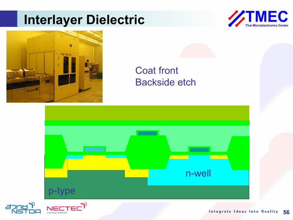
Coat frontBackside etch
p-type
n-well
Interlayer Dielectric

5757
Resist strip
p-type
n-well
Interlayer Dielectric

5858
Process flow
p-type Silicon Substrate
1. Starting wafer2. n-well3. Active4. Gate5. Junction6. ILD7. Contacts and metal 18. Vias and metal 29. Passivation

5959
Contacts and Metal1
Photolithography : CONTACT
p-type
n-well
6060
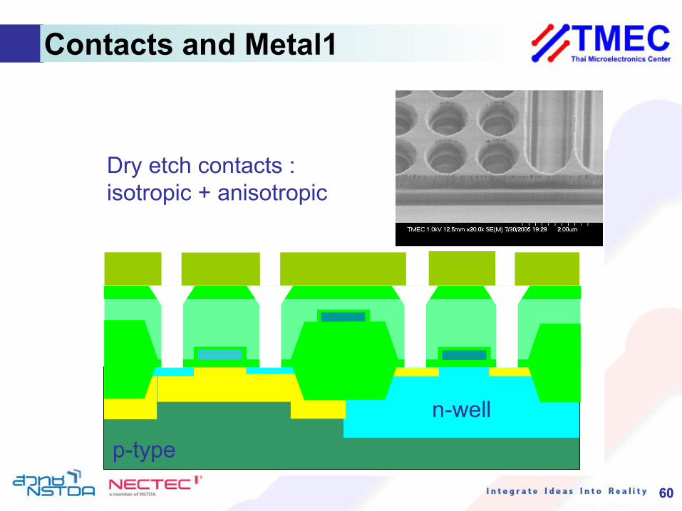
Dry etch contacts : isotropic + anisotropic
p-type
n-well
Contacts and Metal1

6161
Resist strip
p-type
n-well
Contacts and Metal1
6262
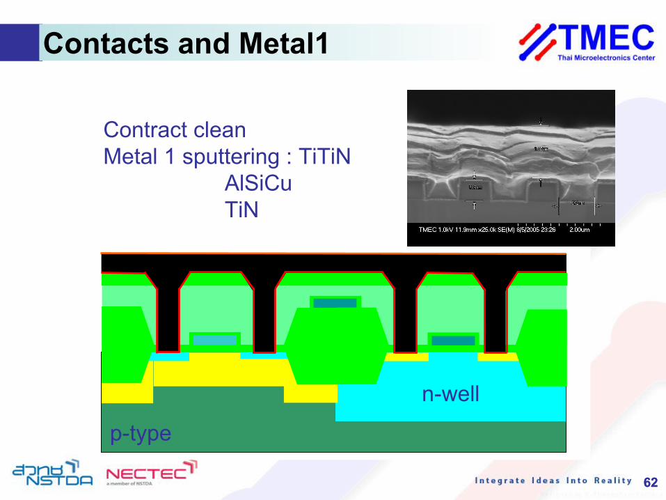
Contract cleanMetal 1 sputtering : TiTiN
AlSiCu TiN
p-type
n-well
Contacts and Metal1

6363
Photolithography : METAL1
p-type
n-well
Contacts and Metal1

6464
Dry etch Metal 1
p-type
n-well
Contacts and Metal1

6565
Resist strip
p-type
n-well
Contacts and Metal1

6666
Process flow
p-type Silicon Substrate
1. Starting wafer2. n-well3. Active4. Gate5. Junction6. ILD7. Contacts and metal 18. Vias and metal 29. Passivation

6767
Via and Metal2
Plasma oxide deposition
p-type
n-well

6868
SOG coatSOG cure
p-type
n-well
Via and Metal2

6969
Plasma oxide deposition
p-type
n-well
Via and Metal2

7070
Photolithography : VIA
p-type
n-well
Via and Metal2
7171
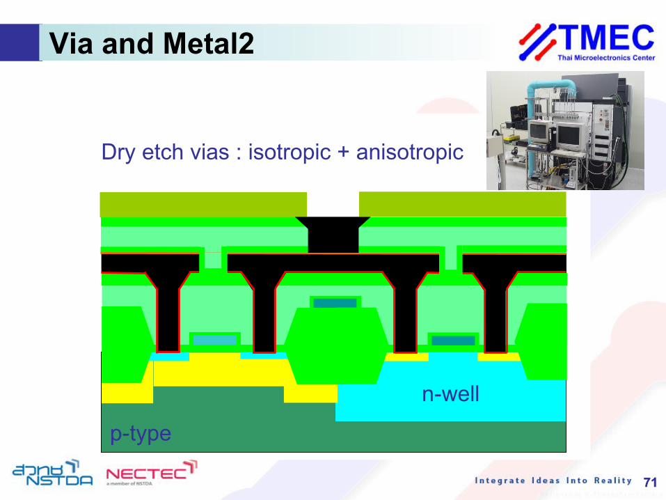
Dry etch vias : isotropic + anisotropic
p-type
n-well
Via and Metal2

7272
Resist strip
p-type
n-well
Via and Metal2

7373
Metal2 sputtering : AlsiCu TiN
p-type
n-well
Via and Metal2

7474
Photolithography : METAL2
p-type
n-well
Via and Metal2

7575
Dry etch metal2
p-type
n-well
Via and Metal2
7676
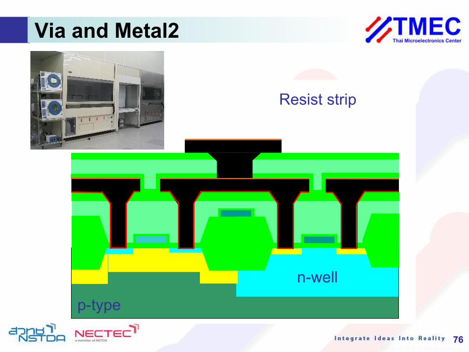
Resist strip
p-type
n-well
Via and Metal2

7777
Process flow
p-type Silicon Substrate
1. Starting wafer2. n-well3. Active4. Gate5. Junction6. ILD7. Contacts and metal 18. Vias and metal 29. Passivation

7878
Passivation
PECVD nitride deposition, Photolithography : PASS, Dry etch nitride, Resist strip, Sintering : Forming gas
p-type
n-well