Wafer Clean and Wet Processing - Välkommen till KTH 3... · Piranha(SPM :sulfuric/peroxide ......
46
Wafer Clean and Wet Processing Lecture 3
Transcript of Wafer Clean and Wet Processing - Välkommen till KTH 3... · Piranha(SPM :sulfuric/peroxide ......

Wafer Clean and Wet Processing
Lecture 3

• Czochralski (CZ) Method
• Float Zone (FZ) Method
• From Ingot to Wafer
• Gettering
• Silicon-on-Insulator (SOI)
PS: For a short video of the wafer production process see:
http://www.siltronic.com/int/en/press/film/film-overview.jsp
Lecture 2: Wafer Fabrication and Silicon Epitaxy
Recap Wafer Fabrication

• Definition and Terminology
• Chemical Vapor Deposition (CVD) / Vapor Phase Epitaxy (VPE)
• Grove Model: Mass-transport vs. Surface Reaction Limited Regime
• Reactors
• Chemistry
• Reactor Types
• Applications
Lecture 2: Wafer Fabrication and Silicon Epitaxy
Recap Silicon Epitaxy

“Where we are today”
Lecture 3: Wafer Clean and Wet Processing
Wafer Fabrication
FEOL Processes
BEOL Fabrication
Packaging
Future Technologies
Device Integration
Simulation & Modeling
Metrology
Electrical Testing
PS: This list of co-dependencies is
not complete!

Lecture 3: Outline
Part 1
• Clean Rooms
• Wafer Cleaning
• Gettering
Part 2
• Silicon Run 1

IH2655 Spring 2010
Christoph Henkel / Mikael Östling KTH 6
ITRS Roadmap: Defining the term “clean”
Introduction

IH2655 Spring 2010
Christoph Henkel / Mikael Östling KTH 7
Three tiered approach
1. Clean Factories (Clean Room)
2. Wafer Cleaning
3. Gettering
Modern IC factories employ a three tiered approach to controlling unwanted
impurities:
Introduction: “Dirt is a natural part of life.”
IH2655 Spring 2010
Christoph Henkel / Mikael Östling KTH 8
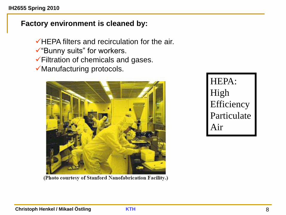
Factory environment is cleaned by:
HEPA filters and recirculation for the air.
“Bunny suits” for workers.
Filtration of chemicals and gases.
Manufacturing protocols.
HEPA:
High
Efficiency
Particulate
Air

IH2655 Spring 2010
Christoph Henkel / Mikael Östling KTH 9
1. Air cleaning
From Intel Museum

IH2655 Spring 2010
Christoph Henkel / Mikael Östling KTH 10

IH2655 Spring 2010
Christoph Henkel / Mikael Östling KTH 11
Electrum Laboratory
ISO Class 6 = Class 1000
ISO Class 5 (Cleanroom Class 100) in APL Litho Room

IH2655 Spring 2010
Christoph Henkel / Mikael Östling KTH 12
HEPA Filter
Exhaust
Thin Porous Sheets
(ultrafine glass
fibers): Large
particles are
trapped by filters
and small particles
are adsorbed by
electrostatics
Recircu
latio
n
20~22C
40~46%RH

IH2655 Spring 2010
Christoph Henkel / Mikael Östling KTH 13
Unwanted impurities must be kept below the ppm or ppb range
Critical (Fatal) Defect (Particle) Size = 1/2 Minimum Feature Size
ITRS Feature Year 2007 2010 2013 2016 2020
Minimum Feature
Size(nm)
65 45 32 22 14
Particle
Organics: Oil,Photoresist
Metal/Alkali ions
Native oxide
Three tiered approach
clean room
wafer cleaning
gettering

IH2655 Spring 2010
Christoph Henkel / Mikael Östling KTH 14
Lecture 3: Outline
Part 1
• Clean Rooms
• Wafer Cleaning
• Contamination Sources
• Cleaning Methods
• Gettering
Part 2
• Silicon Run 1

IH2655 Spring 2010
Christoph Henkel / Mikael Östling KTH 15
Contaminants may consist of particles,
organic films (photoresist), heavy metals
or alkali ions.
Wafer Cleaning: If a Clean Room is not enough

IH2655 Spring 2010
Christoph Henkel / Mikael Östling KTH 16
Various particles deposited on chips
IH2655 Spring 2010
Christoph Henkel / Mikael Östling KTH 17
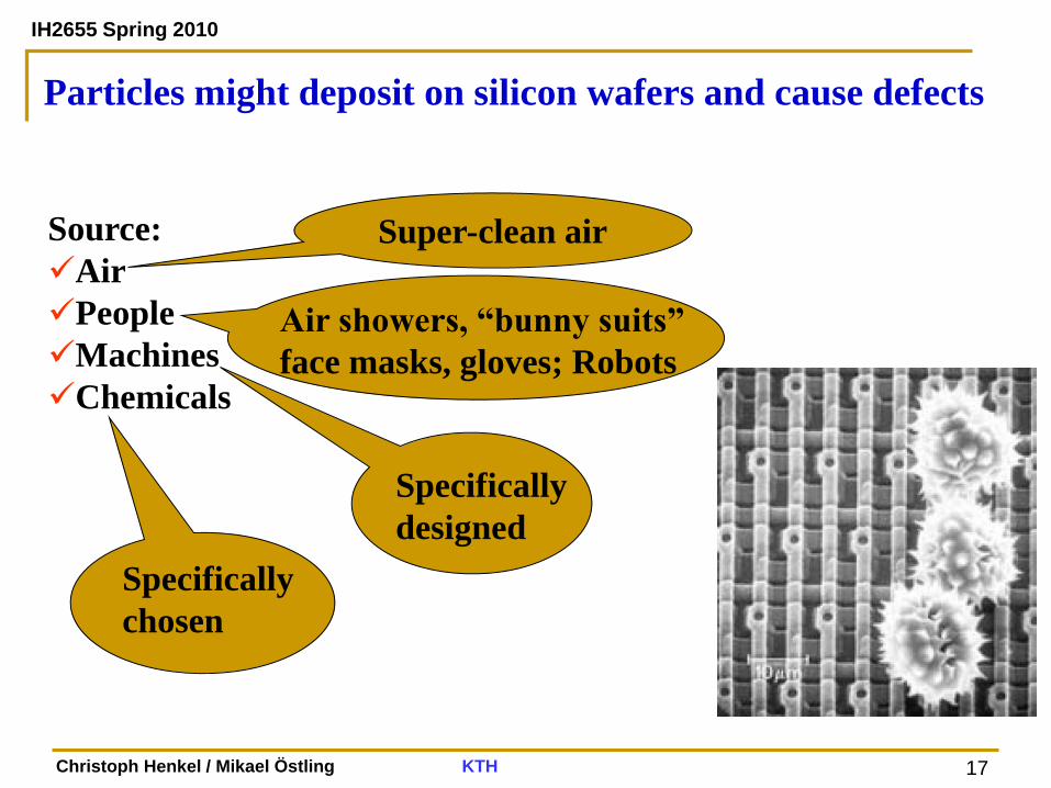
Particles might deposit on silicon wafers and cause defects
Source:
Air
People
Machines
Chemicals
Super-clean air
Air showers, “bunny suits”
face masks, gloves; Robots
Specifically
designed
Specifically
chosen

IH2655 Spring 2010
Christoph Henkel / Mikael Östling KTH 18
>0.2mm >0.5mm
NH4OH 130-240 15-30
H2O2 20-100 5-20
HF 0-1 0
HCl 2-7 1-2
H2SO4 180-1150 10-80
Particle concentration in ULSI chemicals (/ml)

IH2655 Spring 2010
Christoph Henkel / Mikael Östling KTH 19
Example for a metal
organic precursor.
Trimethyl-aluminum.

IH2655 Spring 2010
Christoph Henkel / Mikael Östling KTH 20
Metal Contamination
Source: Chemicals, Processes such as Ion
implantation, Reactive Ion etching, etc.
Magnitude:1010 atom/cm2
Effects:
Cause defects in interfaces, influence device
performance and reduce product yield
Increase leakage current of p-n junction,
decrease lifetime of minority carriers
Fe, Cu, Ni,
Cr, W, Ti…
Na, K, Li…

IH2655 Spring 2010
Christoph Henkel / Mikael Östling KTH 21
Metal contamination
from different processes
Resist Strip
Dry etching
Ion Implantation
Wet oxidation
9 10 11 12 13 Log (concentration/cm2)
Fe Ni Cu

IH2655 Spring 2010
Christoph Henkel / Mikael Östling KTH 22
Organic Contaminations
Source:
• Ambient organic vapors
• Storage containers
• Photoresist residues
Removal methods:Strong oxidation
- Ozone dry
- Piranha:H2SO4-H2O2
- Ozonized ultrapure water

IH2655 Spring 2010
Christoph Henkel / Mikael Östling KTH 23
Native Oxide
Rapid growth in air or water
Problems Increase contact resistance
Difficult to achieve selective CVD or epitaxy
Become sources of metal impurities
Difficult to grow metal silicides
Clean Process:HF+H2O(ca. 1: 50)

IH2655 Spring 2010
Christoph Henkel / Mikael Östling KTH 24
All components and interconnects in ICs are small contaminations by dust
and metals during manufacturing likely lead to malfunctioning devices or
circuits through short or open defects
About 75% of the yield loss in a modern silicon IC manufacturing plant is due
directly to defects caused by particles on the wafer.
Example 1. For an IC manufacturing plant, its output is 1000 wafer/week ×
100 chip/wafer and the chip price is $50/chip. The plant is breakeven if the
product yield is 50%. In order for an annual profit of $10,000,000, the product
yield should increase by
Increasing the product yield by 3.8%, gives
rise to the annual profit of 10 million dollars!
Annual throughput
=Annual expense
=1000×100×52×$50
=$260,000,000
%8.35250$1001000
101$ 7
Harm of the unwanted impurity

IH2655 Spring 2010
Christoph Henkel / Mikael Östling KTH 25
Harm of the unwanted impurity
Example 2. Effects of alkali ions on MOS threshold voltage
ox
M
ox
fAs
fFBth C
C
qNVV
)2(22
If tox=10 nm, when QM=6.5×1011 cm-2(10 ppm), ΔVth=?? V
Example 3. Request of MOS DRAM refresh time on trap density Nt
Typically,
= 10-15 cm2, vth= 10-7 cm/s
So R=100 ms requires
Nt 1012 cm-3 =0.02 ppb !!
tthG Nv 1R

IH2655 Spring 2010
Christoph Henkel / Mikael Östling KTH 26
Lecture 3: Outline
Part 1
• Clean Rooms
• Wafer Cleaning
• Contamination Sources
• Cleaning Methods
• Gettering
Part 2
• Silicon Run 1

IH2655 Spring 2010
Christoph Henkel / Mikael Östling KTH 27
Piranha(SPM:sulfuric/peroxide mixture)
H2SO4(98%):H2O2(30%)=2:1~4:1
Oxidize photoresist into CO2+H2O
(applicable to almost all organics)
Wafer Cleaning: Removing Organics
Two methods
to remove
Organics/
Photoresists Oxygen Plasma Dry Etching:
Oxidize photoresist into gaseous CO2+H2O (applicable to most polymer films)
Note: High-temperature process will drive contaminant
into silicon wafer or thin films
Front-end (FEOL) cleaning is crucially important
Metal

IH2655 Spring 2010
Christoph Henkel / Mikael Östling KTH 28
SC-1(APM,Ammonia Peroxide Mixture):
NH4OH(28%):H2O2(30%):DIH2O=1:1:5~1:2:7
70~80C, 10min Basic (pH>7)
-> DIH2O = De-ionized water
Oxidize organic films
Complex metals
Dissolve slowly native oxide and reoxidize wafer
— help to dislodge particles
NH4OH etches silicon
RCA——Standard Cleaning
OH-
OH-
OH-
OH-
OH-
OH-
RCA clean is
“standard process”
used to remove
organics,
heavy metals and
alkali ions.
Co Ni Cu Zn
Ag Cd
Au Hg
Wafer Cleaning: Standard Clean 1

IH2655 Spring 2010
Christoph Henkel / Mikael Östling KTH 29
SC-2:
HCl(73%):H2O2(30%):DIH2O=1:1:6~1:2:8
70~80C, 10min Acid (pH<7)
Remove alkali ions and cations like Al3+, Fe3+and Mg2+
that form NH4OH-insoluble hydroxides in SC-1 solution
Complete the removal of metallic contaminates such as Au
Combination between RCA and ultrasonic agitation (20~50kHz
or around 1MHz) is quite effective for particle removal.
The sound waves parallel to the silicon wafer infiltrate particles.
Afterwards, solution can diffuse into the wafer surface and the particles
become completely soaked and then suspended freely in the solution.
RCA——Standard Cleaning
Wafer Cleaning: Standard Clean 2

IH2655 Spring 2010
Christoph Henkel / Mikael Östling KTH 30
• RCA clean is “standard process” used to remove organics,
heavy metals and alkali ions.

IH2655 Spring 2010
Christoph Henkel / Mikael Östling KTH 31
Other Advanced Wet Cleaning Technology, e.g. Ohmi
From IMEC (Interuniversity Microelectronic Center)
(1) H2O + O3 (<1 ppb)
Remove Organics
(2) NH4OH +H2O2 +H2O (0.05:1:5)
Remove Particle, Organics and Metals
(3) HF (0.5%) +H2O2 (10%)
Remove Native Oxide and Metals
(4) DI H2O cleaning(>18M-cm)

IH2655 Spring 2010
Christoph Henkel / Mikael Östling KTH 32
Cleaning Equipment
Ultrasonic Cleaning Spray Cleaning
Liquid
Sound
Power
Non-Sound
Transmitter
To Eletrical
Control Module
Nozzle
Shaft
Shell

IH2655 Spring 2010
Christoph Henkel / Mikael Östling KTH 33
Robot-assisted automatic cleaning station

IH2655 Spring 2010
Christoph Henkel / Mikael Östling KTH 34
Container and Carrier Cleaning
SC1/SPM/SC2
– Quartz or Teflon container
HF
– Prefer Teflon. Other colorless plastic containers
are also viable.
Silicon wafer carrier
– Only Teflon or Quartz carriers can be used

IH2655 Spring 2010
Christoph Henkel / Mikael Östling KTH 35
Problems in Wet Cleaning(1)
Surface Roughness: Cleaning
agents and metal contaminants
may etch silicon wafer and result
in micro-roughness on the surface.
High-concentration NH4OH in SC-
1 may etch and damage the silicon
surface.
Reduce the carrier mobility in the
channels
Have devastating effects on the
quality and breakdown voltage of
thermally-grown gate oxide.
Ra
(nm
)
Mixing ratio of NH4OH(A) in NH4OH+H2O2+H2O
solution (A:1:5, A<1)
How to reduce micro-roughness
• Reduce NH4OH concentration
• Reduce cleaning temperature
• Reduce cleaning time

IH2655 Spring 2010
Christoph Henkel / Mikael Östling KTH 36
Introduce particles
Difficult to Dry
Cost
Chemical waste disposal
Incompatible with advanced integrated
technology
Problem in Wet Cleaning(2)

IH2655 Spring 2010
Christoph Henkel / Mikael Östling KTH 37
Dry Cleaning Technology
Gas Chemistry. Usually activation energy is needed to enhance
chemical reactions at low temperatures.
The required energy may come from plasma, ion beam,
shortwave radiation and heating. The energy is used to clean
silicon wafers, but must be prevented from damaging them.
HF/H2O Gas Cleaning
Ultraviolet Ozone Cleaning(UVOC)
H2/Ar Plasma Cleaning
Heat Cleaning

IH2655 Spring 2010
Christoph Henkel / Mikael Östling KTH 38
Lecture 3: Outline
Part 1
• Clean Rooms
• Wafer Cleaning
• Gettering
Part 2
• Silicon Run 1

IH2655 Spring 2010
Christoph Henkel / Mikael Östling KTH 39
Level 3 Contamination Reduction: Gettering • Gettering is used to remove metal ions and alkali ionsfrom device active
regions.
These elements tend to have very high
diffusivities and be easily captured in regions
with either mechanical defects or chemical traps.
Gettering

IH2655 Spring 2010
Christoph Henkel / Mikael Östling KTH 40
Capture defects at locations far away from the device region.
Damaged region will act as "sink" for unwanted elements.
Metals diffuse as interstitials (>> diffusivity than dopants)
Metals need defects to become trapped:
• Dislocations
• Stacking faults
• Grain boundaries
• Precipitates (e.g. O2)
PSG captures alkali ions
(Phosphosilicate Glas)
Gettering
General Stategy
1. Free impurities
2. Diffuse to gettering site
3. Trap at gettering site

IH2655 Spring 2010
Christoph Henkel / Mikael Östling KTH 41
Aus+I AuI “kick-out” mechanism
Aus AuI+ V “dissociative” mechanism
Introduction of a large number of interstitial silicon atoms
may convert substitutional atoms, such as Au and Pt, to
interstitial atoms and hence increase their diffusivity.
Method High-concentration phosphorous diffusion
Ion implantation damage
SiO2 precipitates
Release Mobile, increase diffusivity.
Substitutional atom Interstitial atom
Gettering

IH2655 Spring 2010
Christoph Henkel / Mikael Östling KTH 42
• Heavy metal gettering relies on:
• Metals diffusing very rapidly in silicon
• Metals segregating to “trap” sites.
Gettering: Metals

IH2655 Spring 2010
Christoph Henkel / Mikael Östling KTH 43
•“Trap” sites can be created by SiO2 precipitates (intrinsic gettering), or by
backside damage (extrinsic gettering).
• In intrinsic gettering, CZ silicon is used and SiO2 precipitates are formed in
the wafer bulk through temperature cycling at the start of the process.
Gettering: Metals

IH2655 Spring 2010
Christoph Henkel / Mikael Östling KTH 44
PSG —— Form stable complexes that bind alkali ions
At temperatures above room temperature, alkali ions will easily diffuse to
and be trapped by PSG layers
Clean Processing + Si3N4 cap layer
—— Barriers to indiffusion of alkali ions
Metal ions Gettering
Intrinsic Gettering —— Drive oxygen atoms in silicon from the near
surface region, up to 10~20 mm in depth, into the bulk and reduce the oxygen
concentration within the near surface region to below 10 ppm. The SiO2
precipitates in the silicon bulk create the trap sites for gettering.
Extrinsic Gettering —— Create defects or traps sites for gettering by
producing damage or depositing poly-silicon films on the backside.
Subsequent high-temperature processing step will allow metal ions to diffuse
to the backside and complete the gettering simultaneously.
Gettering

IH2655 Spring 2010
Christoph Henkel / Mikael Östling KTH 45
Contaminations: Particles,
Organics, Metals, Native oxide
Summary of Key Ideas
3 Levels: Clean room, Wafer cleaning and Gettering
The bottom line
is chip yield.
“Bad” die
manufactured
alongside
“good” die.
Increasing yield
leads to better
profitability in
manufacturing
chips.
Native oxide
Strong
Oxidation
HF:DI H2O
Cleaning Class
Efficient Cleaning
Cleaning
Necessity
Devices: Minority carrier lifetime, VT
changes, Ion Ioff, Gate breakdown
voltage , Reliability
Circuit: Yield, Electrical performance
IH2655 Spring 2010
Christoph Henkel / Mikael Östling KTH 46
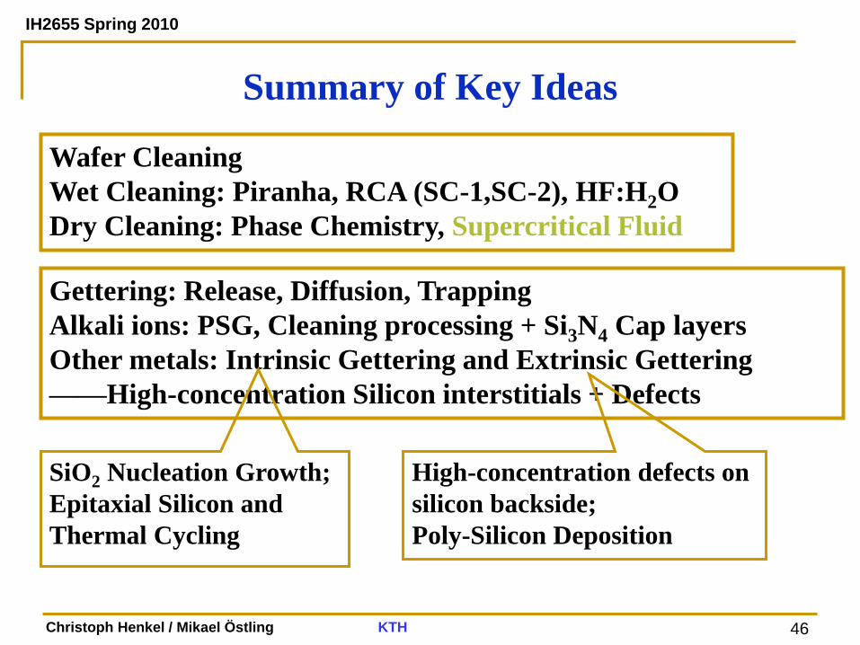
Summary of Key Ideas
Wafer Cleaning
Wet Cleaning: Piranha, RCA (SC-1,SC-2), HF:H2O
Dry Cleaning: Phase Chemistry, Supercritical Fluid
Gettering: Release, Diffusion, Trapping
Alkali ions: PSG, Cleaning processing + Si3N4 Cap layers
Other metals: Intrinsic Gettering and Extrinsic Gettering
——High-concentration Silicon interstitials + Defects
SiO2 Nucleation Growth;
Epitaxial Silicon and
Thermal Cycling
High-concentration defects on
silicon backside;
Poly-Silicon Deposition