W2013
10
DEMULTIPLEXING EQUIPMENT 165 DEMULTIPLEXING EQUIPMENT During the past two decades, there has been rapid advance- ment in optical fiber communication technology. The reduc- TDM .... b b b a c b a c .... a a .... c c tion of single-mode fiber losses, the advent of fiber amplifiers, Figure 2. Interleaving of tributary data streams for the high-bit-rate the improved optical receiver sensitivity, and the develop- data stream. ment of high-speed semiconductor laser diodes and fiber la- sers have promoted the development of multiple access opti- cal fiber networks. The multiple access networks are used to support communications of many users or channels simulta- time division multiplexing system that allows many users or channels to share the high-speed communication link. neously over a common network communication medium. When multiple users or channels are involved, there are two An example of TDM of three tributary bit streams is given in Fig. 2. Each tributary stream is divided into group of bits, primary issues to be addressed. These two issues are how to address the contention that is inherent in sharing a single known as time-slots. All input time-slots are interleaved to yield the output bit stream that has higher data rate than the communication medium and how to synchronize all the users or channels of the network to resolve the contention. The ex- input ones. The time-slot can contain one bit. The result of the TDMA is bit-interleaving. This approach requires only isting optical multiple access networks include wavelength di- vision multiple access (WDMA) networks, subcarrier multiple storage of one bit at each communication node at any time. It is attractive in terms of minimal memory space at each node. access (SCMA) networks, code division multiple access (CDMA) networks, and time division multiple access (TDMA) However, the requirement of bit-synchronization is difficult to achieve in high-bit-rate data streams in optical fiber net- networks (1). On this subtopic we focus on the demultiplexing equipment for optical TDMA networks. works. When the time-slot covers more than one bit, the TDMA is block-based interleaving. The block-based TDMA can be subdivided into two distinct classes: frame-based or TDMA NETWORKS packet-based. Here a frame on the high-speed output bit stream is defined as the collection of bits corresponding to one The most common method of separating users or channels on time-slot from each tributary bit stream. For the example of a common digital communication medium is by ensuring that Fig. 2, one frame corresponds to time-slots a, b, and c. A the signals are transmitted at different times. This technique packet, on the other hand, is an information group with vari- is known as time division multiple access (TDMA). The opti- able size. It allows mixing of bit streams from different users cal fiber communication medium can support high aggregate that vary in bit rate and dynamically allocates the available data rate signal transmission, while the data rates are often bandwidth among these users. There can be different packet lower at user channels. In this case, high-speed optical fiber sizes in the networks. There are also additional overhead bits transmission links can be shared by many lower-speed users. or headers added to each frame or packet to signal the begin- The cost of the high-speed link divided by the number of users ning and ending of the data frame or data packet and to ad- can be significantly lower than the cost of an equivalent set dress the data frame or packet to be routed by the network of lower-speed links. To realize the high-speed link sharing, switches. The additional overhead is useful for demultiplexers it is desired to divide a high-speed bit stream over a point-to- to ensure correct correspondence between input and output point communication link into a set of lower-speed bit tributary bit streams and for network nodes to ensure correct streams, each with a predefined fixed bit rate. The technology routing the data streams. for doing so is called time division multiplexing (TDM). The Regardless of the types of TDMA used, whether bit- or lower-speed bit streams to be multiplexed are called tributary block-based interleaving, the physical bit rate of the TDMA streams. TDM techniques are used to interleave these tribu- date stream is roughly equal to the number of users or nodes tary streams to obtain higher rate bit streams for the high- N connected to the network times the input–output data rate speed communication link. Figure 1 shows a schematic of a (B bit/s) at each node or user. The network must be able to process at the data rate of NB bit/s. Current optoelectronic transceivers can operate at up to 10 Gbit/s (2) and are com- mercially available from Ortel Corporation, for example. Cur- rent network capacity is limited by this data rate. Using higher-speed all-optical switches and demultiplexers, under research and development, the network capacity can be a lot higher. The implementation of optical TDMA involves three impor- tant issues: (a) ranging, (b) synchronization, and (c) optical power leveling. Optical transceivers implementing these three functions are called burst-mode transceivers (3,4). Due to the varying propagation distances between the network nodes and the network controller, to avoid data block overlap- Low-speed links from users Low-speed links to users Time division demultiplexing High-speed link Time division multiplexing .... .... ping (collision), a technique to virtually equalize the connec- tion distance from all nodes to the network controller is re- Figure 1. Schematic of time division multiplexing and demultiplex- quired. The ranging process is to insert a suitable electronic ing to allow users or channels to share a high-speed communication link. delay at each node so that all nodes appear at the same rela- J. Webster (ed.), Wiley Encyclopedia of Electrical and Electronics Engineering. Copyright # 1999 John Wiley & Sons, Inc.
-
Upload
miki-arsovski -
Category
Documents
-
view
213 -
download
0
Transcript of W2013

DEMULTIPLEXING EQUIPMENT 165
DEMULTIPLEXING EQUIPMENT
During the past two decades, there has been rapid advance-ment in optical fiber communication technology. The reduc-
TDM.... b b ba c ba c
.... a a
.... c c
tion of single-mode fiber losses, the advent of fiber amplifiers,Figure 2. Interleaving of tributary data streams for the high-bit-ratethe improved optical receiver sensitivity, and the develop-data stream.ment of high-speed semiconductor laser diodes and fiber la-
sers have promoted the development of multiple access opti-cal fiber networks. The multiple access networks are used tosupport communications of many users or channels simulta- time division multiplexing system that allows many users or
channels to share the high-speed communication link.neously over a common network communication medium.When multiple users or channels are involved, there are two An example of TDM of three tributary bit streams is given
in Fig. 2. Each tributary stream is divided into group of bits,primary issues to be addressed. These two issues are how toaddress the contention that is inherent in sharing a single known as time-slots. All input time-slots are interleaved to
yield the output bit stream that has higher data rate than thecommunication medium and how to synchronize all the usersor channels of the network to resolve the contention. The ex- input ones. The time-slot can contain one bit. The result of
the TDMA is bit-interleaving. This approach requires onlyisting optical multiple access networks include wavelength di-vision multiple access (WDMA) networks, subcarrier multiple storage of one bit at each communication node at any time. It
is attractive in terms of minimal memory space at each node.access (SCMA) networks, code division multiple access(CDMA) networks, and time division multiple access (TDMA) However, the requirement of bit-synchronization is difficult to
achieve in high-bit-rate data streams in optical fiber net-networks (1). On this subtopic we focus on the demultiplexingequipment for optical TDMA networks. works. When the time-slot covers more than one bit, the
TDMA is block-based interleaving. The block-based TDMAcan be subdivided into two distinct classes: frame-based or
TDMA NETWORKSpacket-based. Here a frame on the high-speed output bitstream is defined as the collection of bits corresponding to one
The most common method of separating users or channels ontime-slot from each tributary bit stream. For the example of
a common digital communication medium is by ensuring thatFig. 2, one frame corresponds to time-slots a, b, and c. A
the signals are transmitted at different times. This techniquepacket, on the other hand, is an information group with vari-
is known as time division multiple access (TDMA). The opti-able size. It allows mixing of bit streams from different users
cal fiber communication medium can support high aggregatethat vary in bit rate and dynamically allocates the available
data rate signal transmission, while the data rates are oftenbandwidth among these users. There can be different packet
lower at user channels. In this case, high-speed optical fibersizes in the networks. There are also additional overhead bits
transmission links can be shared by many lower-speed users.or headers added to each frame or packet to signal the begin-
The cost of the high-speed link divided by the number of usersning and ending of the data frame or data packet and to ad-
can be significantly lower than the cost of an equivalent setdress the data frame or packet to be routed by the network
of lower-speed links. To realize the high-speed link sharing,switches. The additional overhead is useful for demultiplexers
it is desired to divide a high-speed bit stream over a point-to-to ensure correct correspondence between input and output
point communication link into a set of lower-speed bittributary bit streams and for network nodes to ensure correct
streams, each with a predefined fixed bit rate. The technologyrouting the data streams.
for doing so is called time division multiplexing (TDM). TheRegardless of the types of TDMA used, whether bit- or
lower-speed bit streams to be multiplexed are called tributaryblock-based interleaving, the physical bit rate of the TDMA
streams. TDM techniques are used to interleave these tribu-date stream is roughly equal to the number of users or nodes
tary streams to obtain higher rate bit streams for the high-N connected to the network times the input–output data rate
speed communication link. Figure 1 shows a schematic of a(B bit/s) at each node or user. The network must be able toprocess at the data rate of NB bit/s. Current optoelectronictransceivers can operate at up to 10 Gbit/s (2) and are com-mercially available from Ortel Corporation, for example. Cur-rent network capacity is limited by this data rate. Usinghigher-speed all-optical switches and demultiplexers, underresearch and development, the network capacity can be a lothigher.
The implementation of optical TDMA involves three impor-tant issues: (a) ranging, (b) synchronization, and (c) opticalpower leveling. Optical transceivers implementing thesethree functions are called burst-mode transceivers (3,4). Dueto the varying propagation distances between the networknodes and the network controller, to avoid data block overlap-
Low-speedlinks from
users
Low-speedlinks tousers
Timedivision
demultiplexing
High-speed linkTimedivision
multiplexing....
....
ping (collision), a technique to virtually equalize the connec-tion distance from all nodes to the network controller is re-Figure 1. Schematic of time division multiplexing and demultiplex-quired. The ranging process is to insert a suitable electronicing to allow users or channels to share a high-speed communication
link. delay at each node so that all nodes appear at the same rela-
J. Webster (ed.), Wiley Encyclopedia of Electrical and Electronics Engineering. Copyright # 1999 John Wiley & Sons, Inc.

166 DEMULTIPLEXING EQUIPMENT
Figure 3. Operation principle of a demul-tiplexer (DEMUX) and a multiplexer(MUX) in a network node.
ba c ed
Input channel 1
f a c gd
Output channel 1
fMUXDEMUX
g
Input channel 2
b e
Output channel 2Synchronization
Clockrecovery
tive propagation distance from the network controller. Once packet or frame multiplexing and demultiplexing, the switch-ing speed can be even lower.ranging has been performed, quick recovery of the clock phase
of each burst of data coming from different nodes is required.This synchronization process can be achieved using a phase-locked loop (5), an oversampling technique, or all-optical clock OPTICAL SOURCES FOR TDMA NETWORKSrecovery (6–9). There are also variations of burst optical pow-ers received at the network controller sent from different To implement the optical TDMA network, the optical sources
must be stable and provide a train of short pulses in the re-nodes. The receiver thus requires a large dynamic range todiscriminate bits ‘‘0’’ and ‘‘1’’ as quickly as possible (3). turn-to-zero (RZ) format. It must also be a low-duty cycle such
as 1 : 5 at the highest network data rate or line rate. This isWithin the optical TDMA network, there are both spaceand time switches. The different time channels on a particu- different from the electronic TDMA network, which uses
lower repetition-rate pulses for tributary data streams andlar input fiber should be capable of being linked to differentoutput fibers (or space channels). The basic functions of multi- higher repetition-rate pulses for network lines. Optical TDMA
uses same short pulses for tributary data streams and theplexer and demultiplexer are to perform insert-and-dropspace switching and time-slot interchange switching. Figure network lines. The data rate of the tributary data stream is
lower as a result of larger pulse-to-pulse separation, con-3 shows the basic operation of a multiplexer (MUX) and ademultiplexer (DEMUX) for a TDMA network node with two trolled by the tributary data stream modulator, while the net-
work line rate is higher due to the TDM of many such tribu-input channels and two output channels. A complex switchingmatrix can be formed by using a number of such basic MUX tary data streams.
When the user channel data rate is very low (tens of Mbit/and DEMUX elements. The DEMUX performs the ‘‘drop’’function by switching some data blocks from input channel 1 s or below), the network can be implemented using electronic
TDMA. The lower bit-rate channels can be electronic channelsto output channel 2, while the MUX performs the ‘‘insert’’function by adding the input data block from input channel 2 or optical fiber channels or both, while the time division mul-
tiplexed network lines use direct modulation of semiconductorto the data channel from the DEMUX for output channel 1.Synchronization is important both for correct data block in- lasers to generate several hundred Mbit/s to a few Gbit/s line
rate. The multiplexing, demultiplexing, clock recovery, andsertion (multiplexing) and for timely drop-out switching (de-multiplexing). The ‘‘drop’’ and ‘‘insert’’ are for the whole time- synchronization are all handled electronically. Here, we focus
on optical TDMA with a user channel data rate of severalslots which can be based on bits or blocks described above.The switching element must have a fast rise and fall time and hundred Mbit/s and above and with a line rate of several
Gbit/s to tens of Gbit/s.have a high repetition rate capability. If the TDMA is bit-interleaved, the switch repetition rate is equivalent to the line To have such a pulse train at a high data rate such as 20
Gbit/s to 40 Gbit/s, it is not currently practical to use directrate (highest network data rate). If the TDMA is block-inter-leaved, the switch repetition rate can be lower than the line laser modulation. External modulation must be used. Narrow
linewidth, which minimizes the pulse broadening of commu-rate. If the block size is eight bits, for example, the switchingspeed can be one-eighth of the line rate. This relaxes greatly nicating light beams due to spectral dispersion in fiber, is a
basic requirement to the laser sources.the switching speed requirement for the TDMA network andallows better utilization of the enormous capacity of the opti- A distributed feedback laser can be used as light source
with electrical modulation using a high-quality sine wave forcal fiber links since present switching devices are mostly con-trolled by electronics. If the block size is even larger for gain switching. The modulation results in short pulses (�80
DEMULTIPLEXING EQUIPMENT 167
DFB laserPulse laser output
Sine wave
Figure 4. Schematic of a DFB laser driven by a sine wave to producea pulse laser output.
Fiber
Fiber-waveguidepigtail
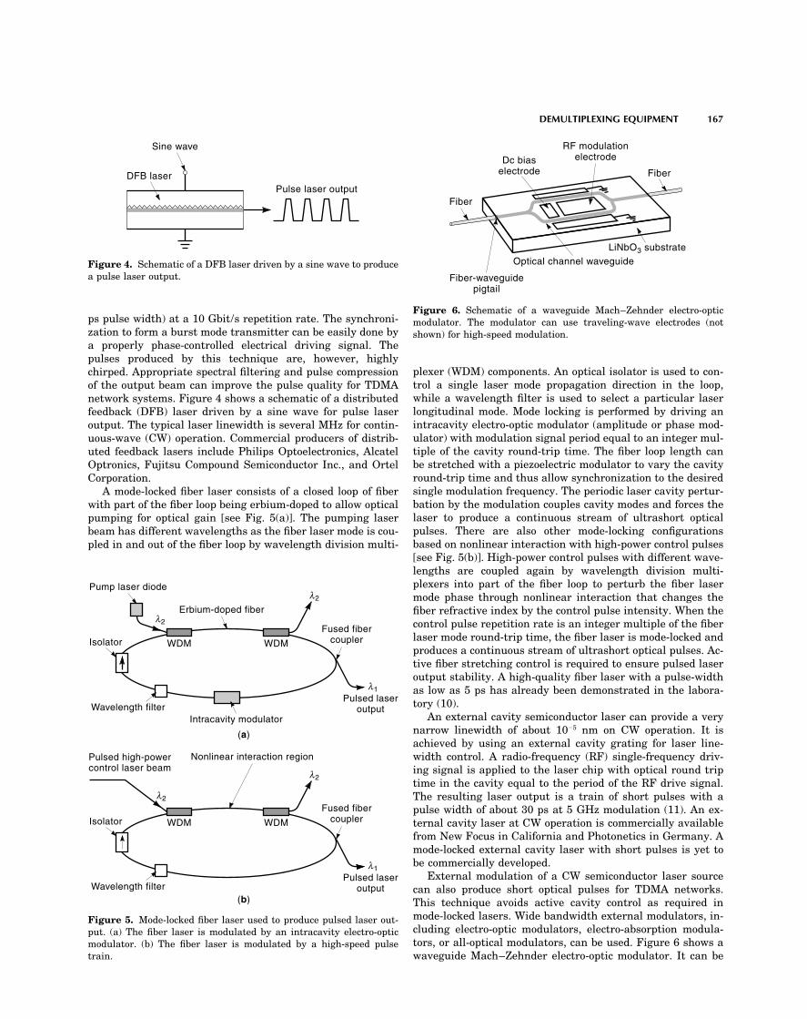
Optical channel waveguideLiNbO3 substrate
Dc biaselectrode
RF modulationelectrode
Fiber
Figure 6. Schematic of a waveguide Mach–Zehnder electro-opticps pulse width) at a 10 Gbit/s repetition rate. The synchroni- modulator. The modulator can use traveling-wave electrodes (notzation to form a burst mode transmitter can be easily done by shown) for high-speed modulation.a properly phase-controlled electrical driving signal. Thepulses produced by this technique are, however, highly
plexer (WDM) components. An optical isolator is used to con-chirped. Appropriate spectral filtering and pulse compressiontrol a single laser mode propagation direction in the loop,of the output beam can improve the pulse quality for TDMAwhile a wavelength filter is used to select a particular lasernetwork systems. Figure 4 shows a schematic of a distributedlongitudinal mode. Mode locking is performed by driving anfeedback (DFB) laser driven by a sine wave for pulse laserintracavity electro-optic modulator (amplitude or phase mod-output. The typical laser linewidth is several MHz for contin-ulator) with modulation signal period equal to an integer mul-uous-wave (CW) operation. Commercial producers of distrib-tiple of the cavity round-trip time. The fiber loop length canuted feedback lasers include Philips Optoelectronics, Alcatelbe stretched with a piezoelectric modulator to vary the cavityOptronics, Fujitsu Compound Semiconductor Inc., and Ortelround-trip time and thus allow synchronization to the desiredCorporation.single modulation frequency. The periodic laser cavity pertur-A mode-locked fiber laser consists of a closed loop of fiberbation by the modulation couples cavity modes and forces thewith part of the fiber loop being erbium-doped to allow opticallaser to produce a continuous stream of ultrashort opticalpumping for optical gain [see Fig. 5(a)]. The pumping laserpulses. There are also other mode-locking configurationsbeam has different wavelengths as the fiber laser mode is cou-based on nonlinear interaction with high-power control pulsespled in and out of the fiber loop by wavelength division multi-[see Fig. 5(b)]. High-power control pulses with different wave-lengths are coupled again by wavelength division multi-plexers into part of the fiber loop to perturb the fiber lasermode phase through nonlinear interaction that changes thefiber refractive index by the control pulse intensity. When thecontrol pulse repetition rate is an integer multiple of the fiberlaser mode round-trip time, the fiber laser is mode-locked andproduces a continuous stream of ultrashort optical pulses. Ac-tive fiber stretching control is required to ensure pulsed laseroutput stability. A high-quality fiber laser with a pulse-widthas low as 5 ps has already been demonstrated in the labora-tory (10).
An external cavity semiconductor laser can provide a verynarrow linewidth of about 10�5 nm on CW operation. It isachieved by using an external cavity grating for laser line-width control. A radio-frequency (RF) single-frequency driv-ing signal is applied to the laser chip with optical round triptime in the cavity equal to the period of the RF drive signal.The resulting laser output is a train of short pulses with apulse width of about 30 ps at 5 GHz modulation (11). An ex-ternal cavity laser at CW operation is commercially availablefrom New Focus in California and Photonetics in Germany. Amode-locked external cavity laser with short pulses is yet tobe commercially developed.
External modulation of a CW semiconductor laser sourcecan also produce short optical pulses for TDMA networks.
Pump laser diode
Wavelength filter
Erbium-doped fiber
Intracavity modulator
(a)
Isolator WDM
Fused fibercoupler
Pulsed laseroutput
λ2λ
λ2λ
λ1λ
WDM
Pulsed laseroutput
λ1λ
Pulsed high-powercontrol laser beam
Wavelength filter
Nonlinear interaction region
(b)
Isolator WDM
Fused fibercoupler
λ2λ
λ2λ
WDM
This technique avoids active cavity control as required inmode-locked lasers. Wide bandwidth external modulators, in-Figure 5. Mode-locked fiber laser used to produce pulsed laser out-cluding electro-optic modulators, electro-absorption modula-put. (a) The fiber laser is modulated by an intracavity electro-optictors, or all-optical modulators, can be used. Figure 6 shows amodulator. (b) The fiber laser is modulated by a high-speed pulse
train. waveguide Mach–Zehnder electro-optic modulator. It can be

168 DEMULTIPLEXING EQUIPMENT
fiber-pigtailed for use as an ultra-high speed modulator. Mod-ulation frequency as high as 50 GHz has already been demon-strated (12). On the commercial level, waveguide Mach–Zehnder electro-optic modulators have been fabricated onLiNbO3 by United Technologies Photonics with a modulationbandwidth of about 18 GHz and a V� of 14.5 V. Both phase
Channel 1
Channel 2
2 1 Switchn GHz, Vπ
Channel 3
Channel 4
2 1 Switchn GHz, V
2 1 Switchn GHz, 2 Vππ
×
×
×
πand amplitude modulation can be integrated on a single de-vice for different system needs. A semiconductor electro-ab- Figure 8. Active multiplexer formed by using several 2 � 1 switches.sorption modulator based on a multiple-quantum-well struc-ture (13) offers the advantage of monolithic integration witha semiconductor laser to form a compact picosecond pulse modulators or electro-absorption modulators, as describedsource chip. It also offers a lower drive voltage than do wave- above. They are not used to shape the pulses. Therefore, thereguide Mach–Zehnder modulator devices. Stable optical pulse is no critical demand on modulator linearity. With a 10 GHztrains with a narrow pulse width of 3.6 ps have been demon- pulse repetition rate and a pulse width of 6 ps, 80 Gbit/s mul-strated (13). An all-optical modulator as shown in Figs. 13 tiplexing has already been demonstrated for communicationand 14, to be discussed below, is currently under research distance of 50 km (14). Passive multiplexers suffer from opti-investigation. The advantages of all-optical modulator are ex- cal coupling loss from the fused fiber star coupler. Erbium-tremely fast, polarization insensitive, and elimination of opti- doped fiber amplifiers or semiconductor optical amplifierscal to electrical conversion. with enough gain must be used to compensate for the optical
power loss due to multiplexing.
MULTIPLEXERS AND DEMULTIPLEXERSActive Multiplexers
The key elements of optical TDMA networks are the time di- It is simple to implement passive optical multiplexers for thevision multiplexers and demultiplexers. The multiplexers TDMA networks. Active multiplexers may provide additionalmay be passive, while the demultiplexers must be active. functions to satisfy some particular network requirements.They are discussed as follows. For example, when there is a need to provide simultaneous
multiplexing and non-RZ to RZ optical format conversion, ac-Passive Multiplexers tive multiplexers composed of several 2 � 1 waveguide elec-
tro-optic switches can be used (see Fig. 8) (15,16). The com-Pulsed digital data from a number of data channels can bemercial 2 � 1 waveguide electro-optic switches are typicallymultiplexed in principle by a passive star coupler. Figure 7based on a Mach–Zehnder structure with a 3 dB directionalshows the schematic of the passive multiplexer. The timingcoupler and are fabricated on LiNbO3. Figure 9 shows theof different data streams arriving at the output star couplerschematic of the 2 � 1 switch. The commercial vendors in-junction can be controlled by variable fiber delay lines by sim-clude New Focus and United Technologies Photonics. Becauseply piezoelectric stretching the fiber lengths. The piezoelectricthe cost of the 2 � 1 switches are significantly higher thanfiber-stretching device can be obtained from Canadian Instru-passive fused fiber star couplers, passive multiplexers are, inmentation and Research Limited with piezoelectric modula-general, more favorable than the active multiplexers. In addi-tion frequency of up to 100 kHz. There is no need for high-tion, active switches introduce a significant insertion lossspeed delay line variation since the synchronization can alsowith typical values of 0 dB to 6 dB for a 2 � 1 switch.be performed on the phase control of the electro-optic modula-
tors which are used as on–off switches to the pulsed opticalActive Demultiplexerslight beams to form the desired pulsed data streams on each
input channel. The modulators can be waveguide electro-optic Unlike the multiplexers that can be passive or active, the de-multiplexers must be active since the drop-out switching froma single channel is time-sensitive. The timing can be con-
Fiber
Fiber-waveguidepigtail
Optical channel waveguideLiNbO3 substrate
Dc bias electrode
3 dB coupler
RF modulationelectrode
Fiber
RF on/offcontrol signal
Electro-opticmodulator
Erbium-dopedfiber amplifier
Fused fiberstar coupler
Fused fiberstar coupleras passive
MUX
Variable opticalfiber delay
Modelockedlaser
Figure 7. Schematic of a passive multiplexer formed by fiber star Figure 9. Schematic of a waveguide 2 � 1 switch with a Mach–Zehnder modulation section and a 3 dB directional coupling section.couplers, modulators, and variable optical fiber delay lines.

DEMULTIPLEXING EQUIPMENT 169
Semiconductor optical amplifier
Data output
Data input
Fused fiberfanout coupler
Figure 12. Active demultiplexer formed by using passive fiber fan-outs and time-gated elimination and amplification of suitable time-slots by semiconductor optical amplifiers.
Channel 1Fused fibercoupler
Receiver Header detectionand clock recovery
Switch driver
Fiber delay line
Channel 2
1 × 2 Switchn GHz, Vπ
Channel 3
Channel 4
1 × 2 Switchn GHz, Vπ
1 × 2 Switchn GHz, 2 Vππ
switching of a short time-slot such as a single bit and can beFigure 10. Active demultiplexer constructed by using several 1 � long for packet switching depending on the packet size.2 switches.
Another implementation of the active demultiplexer isbased on a passive fanout combined with a number of parallel1 � 2 drop-out switches. The schematic of this demultiplexer
trolled through a clock recovery circuit, while the drop-out architecture for 1 to 4 demultiplexing is shown in Fig. 11.switching (space switching) must be performed electro-opti- This type of demultiplexer implementation requires one addi-cally or all-optically. One possible implementation is based on tional 1 � 2 switch and suffers from the fanout optical powera number of cascaded 1 � 2 switches as shown in Fig. 10. loss. Hence, erbium-doped fiber amplifiers or semiconductorThis is a reverse configuration of active multiplexer shown in optical amplifiers are required to compensate for this loss.Fig. 8. The 1 � 2 switch is the same as the 2 � 1 switch but Semiconductor optical amplifiers (17) can also be used tois used differently. For each demultiplexing step, the device implement active demultiplexers (see Fig. 12). It is based oncan be implemented as in Fig. 10 with clock recovery and con- passive fanouts and time gated elimination and amplificationtrol. A small percentage of the optical data stream is taped of suitable time-slots by the semiconductor optical amplifiers.out by a fused fiber coupler to a wide-band receiver that can The semiconductor optical amplifier is a InGaAsP device withbe a pin photodetector with electronic amplifiers. Followed by about �30 dB loss when unbiased and about 10 dB gain whenclock recovery and header detection, a suitable electrical con- biased with �100 mA current. It can be made polarizationtrol signal is then applied to the 1 � 2 switch to perform the insensitive. This simple demultiplexer implementation is at-desired drop-out switching. Since the electrical processing for tractive. The semiconductor optical amplifiers are suppliedclock recovery and header detection is relatively slow and lim- from Alcatel Optronics, for example.ited by the electronic devices, a suitable optical delay is re-quired between the tap fiber coupler and the 1 � 2 switch to Switching Matrixwait for the switching control signal. The optical delay can
When we combine passive multiplexing and active demul-be implemented by a fiber delay line with piezoelectric fibertiplexing based on semiconductor optical amplifiers, any com-stretcher to allow delay time adjustment to synchronize withplex multiplexer and demultiplexer switching matrix can bethe switching control signal. The switch control signal is anformed without much difficulty. To build a compact switchingon–off switching signal. It is not used for pulse shaping. Thematrix, monolithic integration of fan-out components and op-switching signal period must match with the data period oftical amplifiers on a common substrate is required. Such athe drop-out channel. This period can be short for drop-outcompact switching matrix is attractive in terms of minimizingfiber component packaging. Recently, monolithic integrationof a 4 � 4 switch matrix has been successfully demonstratedwith InGaAsP–InP optical amplifiers (18).
Ultrafast All-Optical Polarization InsensitiveSwitches and Demultiplexers
LiNbO3-based 2 � 1, 1 � 2, and 2 � 2 switches are generallypolarization-sensitive. There are significant losses when theseswitches are used in the randomly polarized optical fiber net-works. Suitable electrical signals with voltage amplitudes arerequired for switching control. This needs optical to electricalsignal conversion processing. For fast multiplexing and de-
Drop-out switch
Data output
Data input
Fused fiberfanout coupler
1 × 2
1 × 2
1 × 2
1 × 2multiplexing, it is preferred that the switching be performedall-optically based on the contents of the data stream header.Figure 11. Active demultiplexer formed by using passive fiber fan-To induce an all-optical interaction for switching, the mediumouts and a number of 1 � 2 drop-out switches. Optical amplifiers are
needed to compensate the power loss by the passive fiber fanouts. must be nonlinear. In other words, the refractive index of the

170 DEMULTIPLEXING EQUIPMENT
of �1 while the optical switching control source has carrierwavelength �2. Both wavelengths are centered near the 1.55�m fiber communication wavelengths to minimize the groupdelay caused by fiber dispersion. The switching control sourceis amplified by an erbium-doped fiber amplifier to a powerlevel high enough to effect strong non-linear interaction. Thetwo wavelengths can be combined by a wavelength divisionmultiplexer to a single fiber and launched into the fiber loop.
Data input Control beam input
Data output 1
Data output 23 dB Coupler
Semiconductoroptical amplifier
The fiber coupler has a 50 : 50 coupling ratio for wavelengthFigure 13. Schematic of an ultrafast, polarization insensitive, all-
�1 and 100 : 0 for wavelength �2. The signal beams are nowoptical switching device based on the Mach–Zehnder structure (19).
counterpropagating in the loop while the control beam ispropagating in one direction in the loop as shown. When thesignal beam pulses overlap with control beam pulses propa-medium depend on the light intensity propagating throughgating in the control beam direction, these signal beam pulsesthe medium. Due to the variation of refractive index inducedexperience a � phase shift. The interference of the counter-by light intensity, the light propagating phase is modulated.propagating signal beams at the fiber coupler can thus resultThe phase modulation can be performed by the intensity ofin the ‘‘transmitting’’ of the signal beam to the output fiber orthe same light beam. In this case it is called self-phase modu-the ‘‘reflecting’’ of the signal beam back to the input fiber.lation. The phase modulation can also be performed by an-The reflecting signal beam can be coupled out by another fiberother beam and is known as cross-phase modulation.coupler. The � phase shift can effectively switch the fiber loopSemiconductor optical amplifier medium is a good nonlin-from ‘‘transmitting’’ to ‘‘reflecting’’ or from ‘‘reflecting’’ toear optical medium. When the Mach–Zehnder device struc-‘‘transmitting’’ depending on the fiber loop setup controlled byture is used with two 3 dB couplers and two semiconductora set of polarization controllers (22). In the ‘‘reflecting’’ modeoptical amplifiers, as shown in Fig. 13, the counterpropagat-the switching control signal sends the overlapping signaling control beam can modulate the propagation phases of thepulses to the output while the other pulses are reflected. Inforward-propagating data streams in the two Mach–Zehnderthe ‘‘transmitting’’ mode the switched signal pulses are re-arms. The uneven phase modulation on the two arms resultflected. In either case the drop-out switching for the demul-in the selective coupling into either output channel 1 or out-tiplexer is demonstrated. The reverse operation by sending input channel 2. Ultrahigh-speed all-optical switching with a‘‘insert’’ pulses to overlap with the control pulses can result inswitching window as small as 10 ps has been demonstratedmultiplexing demonstration. The all-optical multiplexing and(19). An 8 ps switching window has also been demonstrateddemultiplexing based on a fiber loop mirror and capable of 2.5on a symmetric Mach–Zehnder all-optical switch (20), and 40Gbit/s to 50 Gbit/s operation has been experimentally demon-Gbit/s demultiplexing using an all-optical clock recovery sig-strated (22–24).nal as a control beam on an all-optical Mach–Zehnder modu-
lator has also been demonstrated (21).Optical fiber is also a nonlinear medium but with a very TIME-SLOT INTERCHANGE SWITCH
small nonlinear Kerr coefficient. With a long fiber length thenonlinear effect in fiber can be significant to facilitate all-opti- Time-slot interchange is another basic function of the TDMA
networks. It allows reconfiguration of the sequence of datacal interaction and thus switching functions. Figure 14 showsa fiber loop mirror structure for all-optical demultiplexing time-slots, including frames and packets, in the network data
streams. The basic function of the time-slot interchange is(22). The input data stream uses optical carrier wavelength
Figure 14. Schematic of a fiber loopstructure for all-optical demultiplexing.
Fiber coupler
Fiber loop
Pulsed switchingbeam generation
Input data stream
Fibercoupler
Reflected beam output
Wavelength divisionmultiplexer
Transmitted beam ouput
Erbium-dopedfiber amplifier
λ2λ
λ2λ
λ1λλ1λ
λ1λ
Clock recoveryand synchronization

DEMULTIPLEXING EQUIPMENT 171
Figure 15. Time-slot interchange switchimplementation using several 2 � 2
Fused fibercoupler
Header frame detectionand clock recovery
Synchronization
4 4
4
3
3Fiber delay 2 × 2 Switch
3
3
2
4 222
Input time-slots Output time-slots
Drop-out time-slots
1
1 1
1
2 × 2 Switch driverswitches.
achieved by dropping a particular time-slot, implementing a ing are demonstrated (25). The key component in time-slotinterchangers is the 2 � 2 electro-optic switch that is similarsuitable time delay using fiber delay lines, and inserting the
time-slot back into the original data stream. The time-slot in- to the 2 � 1 switch but contains two 3 dB directional couplersand thus two input and two output channels.terchange can be used to resolve contention problems. The
sequence of the time-slots in the data streams is now altered. The main drawbacks of LiNbO3-based 2 � 2 switches aretheir high insertion loss of about �4 dB to �6 dB. This limitsThe device implementation of the time-slot interchange
switching can be accomplished by using several cascaded 2 � the number of the 2 � 2 switches to be cascaded in the switch-ing system. Another way to implement the time-slot inter-2 switches with synchronization control and fiber delay. Fig-
ure 15 illustrates the operation function of a time-slot inter- change switch is the parallel approach shown in Fig. 16. Itis based on passive fan-outs and time-gated elimination andchange switch for exchange four time-slot sequences. First, a
fused fiber coupler is used to couple part of the data stream amplification of the desired time-slots using semiconductoroptical amplifiers. This approach requires lower drive voltageout for header detection and clock recovery for synchroniza-
tion purposes. The synchronized switch-driver controls the than the LiNbO3-based switches. It can also facilitate ‘‘insert’’multiplexing function along with the passive multiplexer de-‘‘drop’’ and ‘‘insert’’ functions of the 2 � 2 switches. Fiber de-
lay lines are used to synchronize the data time slots with the scribed above. Current device development is focused on thecombination of fan-out and the semiconductor amplifierswitching signal. For example, the time-slots 2 and 4 of the
original time-slot sequence 1234 are switched out by the first arrays on an integrated substrate. This approach can signifi-cantly minimize the number of fibers to be packaged with the2 � 2 switch while the remaining time-slots are delayed by
the subsequent fiber delay line. The delayed time-slot 3 is time-slot interchange switch unit.then switched out to join with the time-slots 2 and 4, and theremaining time-slot 1 experiences another delay. Then bothtime-slots 3 and 4 are switched back to the original data CLOCK RECOVERY DEVICESstream to yield the new time-slot sequence of 413. The time-slot 2 is dropped out by the time-slot interchange switch in Clock recovery is an important part of the demultiplexer since
it enables correct synchronization of the demultiplexingthis example. Both time-slot interchange and drop-out switch-
Figure 16. Implementation of time-slotinterchange switch using passive fiberfan-outs, semiconductor optical amplifi-
Fused fibercoupler
Header frame detectionand clock recovery
Synchronization
4 4
4
3
Fiber delay
3
3
2
Input time-slots Output time-slots
Drop-out time-slots
1
4 3 2 1
4 3 2 1
4 3 2 1
4 3 2 1
4 3 2 1
1
1
Optical amplifier control
Semiconductoroptical amplifier
Fused fiberstar coupler
2
ers, and fiber delay lines.

172 DEMULTIPLEXING EQUIPMENT
Figure 17. Schematic of an all-opticalclock recovery based on a fiber laser loopand nonlinear interaction with the high-power input data stream.
Data stream input
T
Data stream output
Fiber coupler
Wavelengthfilter
Optical clockoutput
T
Wavelength divisionmultiplexer
Pump laser
Fiberisolator
switching and furthermore on multiplexing switching (see a two-section DFB laser, as shown in Fig. 18, about 18 GHzoptical clock recovery has been demonstrated (9). The self-Fig. 3). There are two types of clock recovery, namely, electri-pulsating mechanism in this case is achieved by dispersivecal and optical clock recoveries. The electrical clock recoveryself-Q-switching. Optical clock recovery using self-pulsatingas shown in Fig. 3 has no difference from those for any otherlaser diode is attractive because the input optical data pulsetransmission system with RZ data input. The optical clockcan be relatively low power and the whole device is small.recovery can be performed by mode-locked fiber laser and by
self-pulsating diode laser. Recently, four-wave mixing tech-nique has also been used for optical clock recovery (26). HEADER DETECTION AND PACKET SWITCHING
Clock Recovery by Mode-Locked Fiber Laser Headers or framing bits have typically been inserted to thedata streams to signal the beginning and ending of the dataPulsed optical data stream with sufficient power can be usedframe or data packet and the address the data to be routed.
to serve as the switching control pulses to control amplitudeBuffering of the incoming data frames or packets with the
or phase of the laser mode in a fiber loop. In the configuration same destination address is required for contention resolu-shown in Fig. 17 incoming data optical pulses propagating in tion. An optical switch must be able to recognize the headerpart of the fiber loop provide a periodic phase perturbation of information to effect the data frame or packet switching.the laser cavity for mode locking (27). Fused fiber couplers The header address can be coded in time or in wavelength.are used to join the fiber loop with the data line. An erbium- For a time-encoded header, the header detection can be ac-doped fiber amplifier is used to ensure enough gain in the complished by specific optical delay lines and by setting thefiber loop. An optical isolator is used to control laser mode photodetector array to be activated by the first header bit thatpropagation direction in the loop while a fiber filter is used experiences the longest delay, and then by comparing withfor laser mode wavelength selection since the fiber loop can the address code of that particular node. If the header addresssupport many resonant mode wavelengths when without a code matches with that of the node, the 2 � 2 switch as shownfilter. Another fiber coupler is used for output coupling the in Fig. 19 is activated to switch the data frame or packet toresonant laser clock. Mode locking occurs when the data pulse this node for further processing. If the header address doesperiod equals to an integer multiple of the laser round-trip not match with that of the node, the switch is not activated.time in the loop. In other words, data pulses with period T, So the data frame or packet continue propagation to the next2T, 3T, and so on, can mode-lock the fiber laser at the period network node. New data frame or packet can also be insertedof T. All-optical clock recovery is thus achieved. A 40 Gbit/s from the node to the network using the 2 � 2 switch with theoptical clock recovery has been demonstrated (6). addition of an optical header.
Clock Recovery by Self-Pulsating Laser Diode
A self-pulsating laser diode consists of two contact sections:one is a forward biased semiconductor laser diode, while theother is a saturable absorber that is weakly biased. The satu-rable absorber section can act as a passive Q switch. The com-bination of laser gain and the saturable absorption results ina stable pulsation behavior. When a pulsed data stream iscoupled into the self-pulsating laser diode, the self-pulsationmay be locked on to the data pulses and produces high-qualityoptical clock pulses at its output. Using this method, a 5 Gbit/s
Self-pulsating DFB laser
Optical clockoutput
Data streaminput
Bias current
optical clock recovery has been demonstrated (8,28). Thespeed of the self-pulsating laser diode using a saturable ab- Figure 18. Two-section self-pulsating DFB laser for all-optical
clock recovery.sorber is limited by the carrier lifetime in the absorber. With

DEMULTIPLEXING EQUIPMENT 173
Figure 19. Example of time-encodedheader detection for TDMA network
Fused fibercoupler
Data stream Time header101011
Fiber delayline
1
0
1
1
1
0
Add data streamto network
Drop data streamto node
To next node
Photodetectorarray
Switch driver
Electronic processing(comparing address code) switching.
For a wavelength encoded header, as shown in Fig. 20, the The time-encoded header detection is typically performedby electronics. Fiber and semiconductor-based optical logicheader can be overlapped with the data frame or packet (16).gates are in the earlier development stage. The wavelengthThe wavelength multiplexing of the header and data streamaddressed header detection is relatively simple and thein the same time window allows better utilization of the fiberswitching control can be faster than the time-encodedcapacity per given time-slot. Group delay due to different dataheader detection.and header wavelengths must be compensated for by intro-
ducing a transmission delay between the header and the datadepending on the known routing length from network node to SUMMARYnetwork node. The detection of the wavelength header can bedone by using a passive wide-band fused fiber coupler with a Optical TDMA networks require timely ‘‘drop’’ and ‘‘insert’’narrow-band wavelength filter, such as a fiber grating device data streams. The ‘‘insert’’ switching is performed by the mul-(29). At each node there is a specific wavelength filter. When tiplexer, while the ‘‘drop’’ switching is performed by the de-the wavelength header passes through the filter, a switching multiplexer. The data stream sequences can be altered by asignal is sent to activate the 2 � 2 switching and thus switch- time-slot interchange switch. The switching pulse period ising the data frame or packet to this node for further pro- controlled by the clock recovered by either electronic or all-cessing. The wavelength header length in time scale is optical means. The system timing is achieved by the headerslightly longer than the data frame or packet length so that detection and synchronization. When the TDMA networks arethe switch will remain open during the data transmit time to block-interleaved, the switching data rate can be significantlyallow the whole data frame or packet to be switched to the lower than the line rate. In this case, the synchronization con-node. When the wavelength header does not pass through the trol can be done by electronics. For faster TDMA switching,fiber filter, the switch is not activated and the whole data the synchronization should be based on the all-optical clockframe or packet passes through the node to the next node. A recovery technique described above.new data frame or packet can also be added to the network Currently, most commercial TDMA networks have line
rates of a few Gbit/s or lower. They are basically electroniccommunication with the addition of a wavelength header.
Figure 20. Detection of wavelength-encoded headers for TDMA network
Fused fibercoupler
Fiber delayline
Spectral filter(fiber grating)
Set switchoff
Add data streamto network
Drop data streamto node
To next node
Set switchon
Switch driverHigh-speedopto-electronic
receiver
Data stream(λd)λ
Wavelengthheader (λh)λ
switching.

174 DENSITY MEASUREMENT
16. A. D. Ellis and D. M. Spirit, The use of GaInAsP amplifiers forTDMA networks with input and output channels being optical40 Gbit/s signal processing, Conf. Nonlinear Guided Wave Phe-fiber channels or a combination of fiber and electronic chan-nomena, Cambridge, MA, 1993, PD2.nels. The input and output fiber channels use opto-electronic
17. D. W. Smith, Optical Network Technology, London: Chapman &transceivers. The multiplexing, demultiplexing, time-slot in-Hall, 1995, pp. 42–43.terchange switching, clock recovery, and synchronization are
18. W. van Berlo et al., Polarization-insensitive, monolithic 4 � 4all handled by electronics. Audio, video, and data can be timeInGaAsP-InP laser amplifier gate switch matrix, IEEE Photon.division multiplexed to yield multimedia TDMA networks.Technol. Lett., 7 (11): 1291–1293, 1995.Higher data rate optical TDMA networks are currently in the
19. K. I. Kang et al., Demonstration of ultrafast, all-optical, low con-infancy of the development. They have the potential to offertrol energy, single wavelength, polarization independent, cascad-a significantly faster data rate and allow better utilization ofable, and integratable switch, Appl. Phys. Lett., 67 (5): 605–607,
the enormous capacity of the optical fiber communication. It 1995.is the future of the TDMA networks. 20. S. Nakamura, K. Tajima, and Y. Sugimoto, Experimental investi-
gation on high-speed switching characteristics of a novel symmet-ric Mach–Zehnder all-optical switch, Appl. Phys. Lett., 65 (3):
BIBLIOGRAPHY 283–285, 1994.21. R. Ludwig et al., 40 Gbit/s demultiplexing experiment with 10
1. D. J. G. Mestdagh, Fundamentals of Multiaccess Optical Fiber GHz all-optical clock recovery using a mode-locked semiconductorNetworks, Norwood, MA: Artech House, 1995. laser, Electron. Lett., 32 (4): 327–329, 1996.
22. B. P. Nelson et al., All-optical Gbit/s switching using nonlinear2. J. Hanenschild et al., Silicon bipolar chipset with maximum dataoptical loop mirror, Electron. Lett., 27 (9): 704–705, 1991.rates from 10 to 23 Gbits/s for optical communications, Electron.
Lett., 27 (25): 2383–2384, 1991. 23. J. P. Sokoloff et al., A terahertz optical asymmetric demultiplexer(TOAD), IEEE Photon. Technol. Lett., 5 (7): 787–790, 1993.3. C. A. Eldering et al., Transmitter and receiver requirements for
24. D. M. Patrick, A. D. Ellis, and D. M. Spirit, Bit-rate flexible all-TDMA passive optical networks, 3rd IEEE Conf. Local Opt. Net-optical demultiplexing using a non-linear optical loop mirror,works, Tokyo, Japan, 1991.Electron. Lett., 29 (8): 702–703, 1993.4. Y. Ota and R. G. Swartz, DC-1Gb/s burst-mode compatible re-
25. D. K. Hunter and D. G. Smith, New architectures for opticalceiver for optical bus applications, J. Lightwave Technol., 10 (2):TDM switching, J. Lightwave Technol., 11 (3): 495–511, 1993.244–249, 1992.
26. O. Kamatani, S. Kawanishi, and M. Saruwatari, Prescaled 6.35. S. Kawanishi and M. Saruwatari, Ultra-high-speed PLL-typeGHz clock recovery from 50 Gb/s TDM optical signal with 50 GHzclock recovery circuit based on all-optical gain modulation inPLL using four-wave mixing in a travelling-wave laser diode opti-traveling-wave laser diode amplifier, J. Lightwave Technol., 11cal amplifier, Electron. Lett., 30 (10): 807–809, 1994.(12): 2123–2129, 1993.
27. K. Smith and J. K. Lucek, All-optical clock recovery using a6. A. D. Ellis, K. Smith, and D. M. Patrick, All optical clock recovery mode-locked laser, Electron. Lett., 28 (19): 1814–1816, 1992.
at bit rates up to 40 Gbit/s, Electron. Lett., 29 (15): 1323–1324,28. P. E. Barnsley et al., A 4 � 5 Gb/s transmission system with all-1993.
optical clock recovery, IEEE Photon. Technol. Lett., 4 (1): 83–86,7. S. Bigo and E. Desurvire, 20 GHz all-optical clock recovery based 1992.
on fibre laser mode-locking with fibre nonlinear loop mirror as 29. R. Kashyap et al., All-fiber narrowband reflection gratings atvariable intensity/phase modulator, Electron. Lett., 31 (21): 1500 nm, Electron. Lett., 26 (11): 730–732, 1990.1855–1856, 1995.
8. P. E. Barnsley et al., All-optical clock recovery from 5 Gb/s RZ MICHAEL R. WANGdata using a self-pulsating 1.56 �m laser diode, IEEE Photon. University of MiamiTechnol. Lett., 3 (10): 942–945, 1991.
9. U. Feiste, D. J. As, and A. Ehrhardt, 18 GHz all-optical frequencylocking and clock recovery using a self-pulsating two-sectionDFB-laser, IEEE Photon. Technol. Lett., 6: 106–108, 1994.
10. M. Jiang et al., Synchronization of passively mode-locked erbium-doped fiber lasers and its application to optical communicationnetworks, J. Lightwave Technol., 15 (11): 2020–2028, 1997.
11. P. B. Hansen et al., 5.5 mm long InGaAsP monolithic extended-cavity laser with an integrated Bragg reflector for active mode-locking, IEEE Photon. Technol. Lett., 4 (3): 215–217, 1992.
12. D. W. Dolfi and T. R. Ranganath, 50 GHz velocity-matched broadwavelength LiNbO3 modulator with multimode active section,Electron. Lett., 28 (13): 1197–1198, 1992.
13. S. Oshiba, K. Nakamura, and H. Horikawa, Low-drive-voltageMQW electroabsorption modulator for optical short-pulse genera-tion, IEEE J. Quantum Electron., 34 (2): 277–281, 1998.
14. S. Kawanishi et al., 100 Gbit/s 50 km optical transmission em-ploying all-optical multi/demultiplexing and PLL timing extrac-tion, Tech. Dig. OFC ’93, 1993, PD2.
15. L. C. Blank, Multi-Gbit/s optical time division multiplexing em-ploying LiNbO3 switches with low frequency sinewave drive,Electron. Lett., 24 (25): 1543–1544, 1988.