w197e12b Sp10 Sp16 Sp20 Operation Manual
176
Cat. No. W197-E1-2B Programmable Controller SYSMAC mini SP10/SP16/SP20
-
Upload
ravinderreddyn -
Category
Documents
-
view
106 -
download
0
Transcript of w197e12b Sp10 Sp16 Sp20 Operation Manual

Cat. No. W197-E1-2B
Programmable Controller
SYSMAC mini
SP10/SP16/SP20
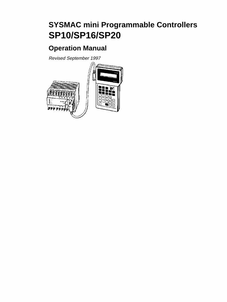
SYSMAC mini Programmable ControllersSP10/SP16/SP20Operation ManualRevised September 1997

!
!
!
ii
Notice:OMRON products are manufactured for use according to proper procedures by a qualified operatorand only for the purposes described in this manual.
The following conventions are used to indicate and classify precautions in this manual. Always heedthe information provided with them. Failure to heed precautions can result in injury to people or dam-age to the product.
DANGER Indicates information that, if not heeded, is likely to result in loss of life or serious injury.
WARNING Indicates information that, if not heeded, could possibly result in loss of life or serious injury.
Caution Indicates information that, if not heeded, could result in relatively serious or minor injury, dam-age to the product, or faulty operation.
OMRON Product ReferencesAll OMRON products are capitalized in this manual. The word “Unit” is also capitalized when it refersto an OMRON product, regardless of whether or not it appears in the proper name of the product.
The abbreviation “Ch,” which appears in some displays and on some OMRON products, often means“word” and is abbreviated “Wd” in documentation in this sense.
The abbreviation “PC” means Programmable Controller and is not used as an abbreviation for any-thing else.
Visual AidsThe following headings appear in the left column of the manual to help you locate different types ofinformation.
Note Indicates information of particular interest for efficient and convenient operationof the product.
1, 2, 3... 1. Indicates lists of one sort or another, such as procedures, checklists, etc.
OMRON, 1991All rights reserved. No part of this publication may be reproduced, stored in a retrieval system, or transmitted, in anyform, or by any means, mechanical, electronic, photocopying, recording, or otherwise, without the prior written permis-sion of OMRON.
No patent liability is assumed with respect to the use of the information contained herein. Moreover, because OMRON isconstantly striving to improve its high–quality products, the information contained in this manual is subject to changewithout notice. Every precaution has been taken in the preparation of this manual. Nevertheless, OMRON assumes noresponsibility for errors or omissions. Neither is any liability assumed for damages resulting from the use of the informa-tion contained in this publication.
iii
About this Manual:
This manual describes the installation and operation of the SYSMAC mini Programmable Controllersand includes the sections described below. The SYSMAC mini PCs include the SP10, SP16, and theSP20 and are called SP-series PCs in this manual. Please read this manual completely and be sureyou understand the information provide before attempting to install and operation any of the SP-se-ries PCs.
Section 1 Introduction explains the background and some of the terms used in ladder-diagram pro-gramming. It also provides an overview of the process of programming and operating a PC andexplains basic terminology used with OMRON PCs. Descriptions of the features of the SP-series PCsand Units that comprise SP-series systems are also provided.
Section 2 Installation provides details on the installation environment and the wiring of the PC. Thedimensions of all components are also presented.
Section 3 Programming describes information necessary for programming SP-series PCs. The firstfive subsections provide enough information to enable you to write, input, and execute a basic ladder-diagram program. The remainder of this section provides more advanced programming information,with 3–7 describing individually each instruction in the SP-series instruction set.
Section 4 Operation provides further information on operating SP-series PCs via the ProgrammingConsole, such as monitoring, data modification, and Memory Card operations.
Section 5 T roubleshooting provides information on error indications. Information in this section isalso necessary when debugging a program.
The appendices provide tables of standard OMRON products available for the SP-series PCs, specifi-cations, reference tables of instructions and Programming Console operations, and error and arithme-tic flag operation. Also provided are several programming and data area assignment sheets that canbe copied out of the manual and used in developing programs.
WARNING Failure to read and understand the information provided in this manual may result in personalinjury or death, damage to the product, or product failure. Please read each section in itsentirety and be sure you understand the information provided in the section and relatedsections before attempting any of the procedures or operations given.
!
v
TABLE OF CONTENTS
PRECAUTIONS ix . . . . . . . . . . . . . . . . . . . . . . . . . . . . . . . . . . . . . . . . . . . . . . . . 1 Intended Audience x . . . . . . . . . . . . . . . . . . . . . . . . . . . . . . . . . . . . . . . . . . . . . . . . 2 General Precautions x . . . . . . . . . . . . . . . . . . . . . . . . . . . . . . . . . . . . . . . . . . . . . . . 3 Safety Precautions x . . . . . . . . . . . . . . . . . . . . . . . . . . . . . . . . . . . . . . . . . . . . . . . . 4 Operating Environment Precautions x . . . . . . . . . . . . . . . . . . . . . . . . . . . . . . . . . . . 5 Application Precautions xi . . . . . . . . . . . . . . . . . . . . . . . . . . . . . . . . . . . . . . . . . . . .
SECTION 1 – Introduction 1 . . . . . . . . . . . . . . . . . . . . . . . . . . . . . . . . . . . . . . . 1-1 Features 2 . . . . . . . . . . . . . . . . . . . . . . . . . . . . . . . . . . . . . . . . . . . . . . . . . . . . . . . . . 1-2 PC Basics 2 . . . . . . . . . . . . . . . . . . . . . . . . . . . . . . . . . . . . . . . . . . . . . . . . . . . . . . .
1-2-1 PC Terminology 3 . . . . . . . . . . . . . . . . . . . . . . . . . . . . . . . . . . . . . . . . . . 1-2-2 Overview of PC Operation 4 . . . . . . . . . . . . . . . . . . . . . . . . . . . . . . . . .
1-3 Units 5 . . . . . . . . . . . . . . . . . . . . . . . . . . . . . . . . . . . . . . . . . . . . . . . . . . . . . . . . . . . 1-3-1 CPU 5 . . . . . . . . . . . . . . . . . . . . . . . . . . . . . . . . . . . . . . . . . . . . . . . . . . . 1-3-2 Programming Console 6 . . . . . . . . . . . . . . . . . . . . . . . . . . . . . . . . . . . . . 1-3-3 Link Adapter 7 . . . . . . . . . . . . . . . . . . . . . . . . . . . . . . . . . . . . . . . . . . . . 1-3-4 Memory Cards 7 . . . . . . . . . . . . . . . . . . . . . . . . . . . . . . . . . . . . . . . . . . .
1-4 PC Configuration 8 . . . . . . . . . . . . . . . . . . . . . . . . . . . . . . . . . . . . . . . . . . . . . . . . . 1-4-1 Basic Configuration 8 . . . . . . . . . . . . . . . . . . . . . . . . . . . . . . . . . . . . . . . 1-4-2 Expanded System Configuration: PC Links 8 . . . . . . . . . . . . . . . . . . . .
SECTION 2 – Installation 11 . . . . . . . . . . . . . . . . . . . . . . . . . . . . . . . . . . . . . . . . 2-1 Dimensions 12 . . . . . . . . . . . . . . . . . . . . . . . . . . . . . . . . . . . . . . . . . . . . . . . . . . . . . . 2-2 Installation 13 . . . . . . . . . . . . . . . . . . . . . . . . . . . . . . . . . . . . . . . . . . . . . . . . . . . . . .
2-2-1 Installation Environment 13 . . . . . . . . . . . . . . . . . . . . . . . . . . . . . . . . . . . 2-2-2 Cooling 14 . . . . . . . . . . . . . . . . . . . . . . . . . . . . . . . . . . . . . . . . . . . . . . . . . 2-2-3 Preventing Noise 14 . . . . . . . . . . . . . . . . . . . . . . . . . . . . . . . . . . . . . . . . . 2-2-4 Mounting Requirements 15 . . . . . . . . . . . . . . . . . . . . . . . . . . . . . . . . . . .
2-3 Wiring 15 . . . . . . . . . . . . . . . . . . . . . . . . . . . . . . . . . . . . . . . . . . . . . . . . . . . . . . . . . . 2-3-1 Power Supply 15 . . . . . . . . . . . . . . . . . . . . . . . . . . . . . . . . . . . . . . . . . . . . 2-3-2 I/O Connections 16 . . . . . . . . . . . . . . . . . . . . . . . . . . . . . . . . . . . . . . . . . . 2-3-3 Precautions 20 . . . . . . . . . . . . . . . . . . . . . . . . . . . . . . . . . . . . . . . . . . . . . .
2-4 Programming Console 20 . . . . . . . . . . . . . . . . . . . . . . . . . . . . . . . . . . . . . . . . . . . . . 2-4-1 Designating the PC 21 . . . . . . . . . . . . . . . . . . . . . . . . . . . . . . . . . . . . . . . 2-4-2 Input Filters 22 . . . . . . . . . . . . . . . . . . . . . . . . . . . . . . . . . . . . . . . . . . . . .
SECTION 3 – Programming 25 . . . . . . . . . . . . . . . . . . . . . . . . . . . . . . . . . . . . . . 3-1 Introduction 27 . . . . . . . . . . . . . . . . . . . . . . . . . . . . . . . . . . . . . . . . . . . . . . . . . . . . . . 3-2 Memory Areas 27 . . . . . . . . . . . . . . . . . . . . . . . . . . . . . . . . . . . . . . . . . . . . . . . . . . .
3-2-1 Data Area Structure 28 . . . . . . . . . . . . . . . . . . . . . . . . . . . . . . . . . . . . . . . 3-2-2 I/O Bits 30 . . . . . . . . . . . . . . . . . . . . . . . . . . . . . . . . . . . . . . . . . . . . . . . . . 3-2-3 Work Bits 31 . . . . . . . . . . . . . . . . . . . . . . . . . . . . . . . . . . . . . . . . . . . . . . . 3-2-4 Dedicated Bits 31 . . . . . . . . . . . . . . . . . . . . . . . . . . . . . . . . . . . . . . . . . . . 3-2-5 LR Area 33 . . . . . . . . . . . . . . . . . . . . . . . . . . . . . . . . . . . . . . . . . . . . . . . . 3-2-6 DR Area 36 . . . . . . . . . . . . . . . . . . . . . . . . . . . . . . . . . . . . . . . . . . . . . . . . 3-2-7 TC (Timer/Counter) Area 36 . . . . . . . . . . . . . . . . . . . . . . . . . . . . . . . . . .
3-3 The Programming Console 37 . . . . . . . . . . . . . . . . . . . . . . . . . . . . . . . . . . . . . . . . . . 3-3-1 The Keyboard 38 . . . . . . . . . . . . . . . . . . . . . . . . . . . . . . . . . . . . . . . . . . . 3-3-2 PC Modes 39 . . . . . . . . . . . . . . . . . . . . . . . . . . . . . . . . . . . . . . . . . . . . . . .
Table of contents
vi
3-4 Basic Programming 39 . . . . . . . . . . . . . . . . . . . . . . . . . . . . . . . . . . . . . . . . . . . . . . . 3-4-1 Terminology 39 . . . . . . . . . . . . . . . . . . . . . . . . . . . . . . . . . . . . . . . . . . . . . 3-4-2 Mnemonic Code 41 . . . . . . . . . . . . . . . . . . . . . . . . . . . . . . . . . . . . . . . . . . 3-4-3 Ladder Instructions 42 . . . . . . . . . . . . . . . . . . . . . . . . . . . . . . . . . . . . . . . 3-4-4 OUTPUT and OUTPUT NOT 44 . . . . . . . . . . . . . . . . . . . . . . . . . . . . . . . 3-4-5 The END Instruction 44 . . . . . . . . . . . . . . . . . . . . . . . . . . . . . . . . . . . . . . 3-4-6 Logic Block Instructions 45 . . . . . . . . . . . . . . . . . . . . . . . . . . . . . . . . . . . 3-4-7 Coding Multiple Right-hand Instructions 51 . . . . . . . . . . . . . . . . . . . . . .
3-5 Inputting the Program 51 . . . . . . . . . . . . . . . . . . . . . . . . . . . . . . . . . . . . . . . . . . . . . . 3-5-1 Initial Programming Console Operation 51 . . . . . . . . . . . . . . . . . . . . . . . 3-5-2 Designating the PC 52 . . . . . . . . . . . . . . . . . . . . . . . . . . . . . . . . . . . . . . . 3-5-3 Clearing Memory 53 . . . . . . . . . . . . . . . . . . . . . . . . . . . . . . . . . . . . . . . . . 3-5-4 Clearing Error Messages 54 . . . . . . . . . . . . . . . . . . . . . . . . . . . . . . . . . . . 3-5-5 Setting and Reading from Program Memory Address 54 . . . . . . . . . . . . 3-5-6 Entering or Editing Programs 55 . . . . . . . . . . . . . . . . . . . . . . . . . . . . . . . 3-5-7 Checking the Program 57 . . . . . . . . . . . . . . . . . . . . . . . . . . . . . . . . . . . . . 3-5-8 Program Transfer 58 . . . . . . . . . . . . . . . . . . . . . . . . . . . . . . . . . . . . . . . . . 3-5-9 Program Searches 61 . . . . . . . . . . . . . . . . . . . . . . . . . . . . . . . . . . . . . . . . 3-5-10 Inserting and Deleting Instructions 61 . . . . . . . . . . . . . . . . . . . . . . . . . . .
3-6 Advanced Programming 64 . . . . . . . . . . . . . . . . . . . . . . . . . . . . . . . . . . . . . . . . . . . . 3-6-1 Interlocks 64 . . . . . . . . . . . . . . . . . . . . . . . . . . . . . . . . . . . . . . . . . . . . . . . 3-6-2 Controlling Bit Status 65 . . . . . . . . . . . . . . . . . . . . . . . . . . . . . . . . . . . . . 3-6-3 DIFFERENTIATE UP and DIFFERENTIATE DOWN 66 . . . . . . . . . . . 3-6-4 KEEP 66 . . . . . . . . . . . . . . . . . . . . . . . . . . . . . . . . . . . . . . . . . . . . . . . . . . 3-6-5 Self-maintaining Bits (Seal) 67 . . . . . . . . . . . . . . . . . . . . . . . . . . . . . . . . 3-6-6 Work Bits (Internal Relays) 67 . . . . . . . . . . . . . . . . . . . . . . . . . . . . . . . . . 3-6-7 Programming Precautions 69 . . . . . . . . . . . . . . . . . . . . . . . . . . . . . . . . . .
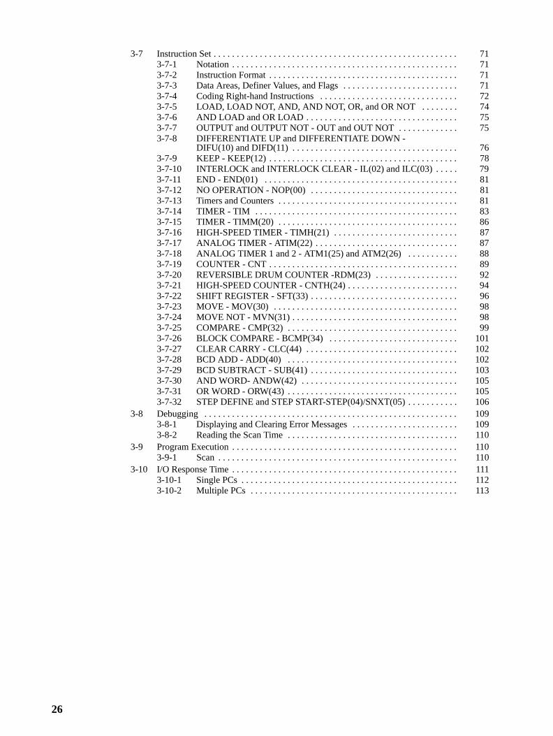
3-7 Instruction Set 71 . . . . . . . . . . . . . . . . . . . . . . . . . . . . . . . . . . . . . . . . . . . . . . . . . . . . 3-7-1 Notation 71 . . . . . . . . . . . . . . . . . . . . . . . . . . . . . . . . . . . . . . . . . . . . . . . . 3-7-2 Instruction Format 71 . . . . . . . . . . . . . . . . . . . . . . . . . . . . . . . . . . . . . . . . 3-7-3 Data Areas, Definer Values, and Flags 71 . . . . . . . . . . . . . . . . . . . . . . . . 3-7-4 Coding Right-hand Instructions 72 . . . . . . . . . . . . . . . . . . . . . . . . . . . . . . 3-7-5 LOAD, LOAD NOT, AND, AND NOT, OR, and OR NOT 74 . . . . . . . . 3-7-6 AND LOAD and OR LOAD 75 . . . . . . . . . . . . . . . . . . . . . . . . . . . . . . . . 3-7-7 OUTPUT and OUTPUT NOT - OUT and OUT NOT 75 . . . . . . . . . . . . 3-7-8 DIFFERENTIATE UP and DIFFERENTIATE DOWN -
DIFU(10) and DIFD(11) 76 . . . . . . . . . . . . . . . . . . . . . . . . . . . . . . . . . . . 3-7-9 KEEP - KEEP(12) 78 . . . . . . . . . . . . . . . . . . . . . . . . . . . . . . . . . . . . . . . . 3-7-10 INTERLOCK and INTERLOCK CLEAR - IL(02) and ILC(03) 79 . . . . 3-7-11 END - END(01) 81 . . . . . . . . . . . . . . . . . . . . . . . . . . . . . . . . . . . . . . . . . . 3-7-12 NO OPERATION - NOP(00) 81 . . . . . . . . . . . . . . . . . . . . . . . . . . . . . . . . 3-7-13 Timers and Counters 81 . . . . . . . . . . . . . . . . . . . . . . . . . . . . . . . . . . . . . . 3-7-14 TIMER - TIM 83 . . . . . . . . . . . . . . . . . . . . . . . . . . . . . . . . . . . . . . . . . . . 3-7-15 TIMER - TIMM(20) 86 . . . . . . . . . . . . . . . . . . . . . . . . . . . . . . . . . . . . . . 3-7-16 HIGH-SPEED TIMER - TIMH(21) 87 . . . . . . . . . . . . . . . . . . . . . . . . . . 3-7-17 ANALOG TIMER - ATIM(22) 87 . . . . . . . . . . . . . . . . . . . . . . . . . . . . . . 3-7-18 ANALOG TIMER 1 and 2 - ATM1(25) and ATM2(26) 88 . . . . . . . . . . . 3-7-19 COUNTER - CNT 89 . . . . . . . . . . . . . . . . . . . . . . . . . . . . . . . . . . . . . . . . 3-7-20 REVERSIBLE DRUM COUNTER -RDM(23) 92 . . . . . . . . . . . . . . . . . 3-7-21 HIGH-SPEED COUNTER - CNTH(24) 94 . . . . . . . . . . . . . . . . . . . . . . . 3-7-22 SHIFT REGISTER - SFT(33) 96 . . . . . . . . . . . . . . . . . . . . . . . . . . . . . . . 3-7-23 MOVE - MOV(30) 98 . . . . . . . . . . . . . . . . . . . . . . . . . . . . . . . . . . . . . . . . 3-7-24 MOVE NOT - MVN(31) 98 . . . . . . . . . . . . . . . . . . . . . . . . . . . . . . . . . . . 3-7-25 COMPARE - CMP(32) 99 . . . . . . . . . . . . . . . . . . . . . . . . . . . . . . . . . . . . 3-7-26 BLOCK COMPARE - BCMP(34) 101 . . . . . . . . . . . . . . . . . . . . . . . . . . . . 3-7-27 CLEAR CARRY - CLC(44) 102 . . . . . . . . . . . . . . . . . . . . . . . . . . . . . . . .

Table of contents
vii
3-7-28 BCD ADD - ADD(40) 102 . . . . . . . . . . . . . . . . . . . . . . . . . . . . . . . . . . . . . 3-7-29 BCD SUBTRACT - SUB(41) 103 . . . . . . . . . . . . . . . . . . . . . . . . . . . . . . . 3-7-30 AND WORD- ANDW(42) 105 . . . . . . . . . . . . . . . . . . . . . . . . . . . . . . . . . 3-7-31 OR WORD - ORW(43) 105 . . . . . . . . . . . . . . . . . . . . . . . . . . . . . . . . . . . . 3-7-32 STEP DEFINE and STEP START-STEP(04)/SNXT(05) 106 . . . . . . . . . .
3-8 Debugging 109 . . . . . . . . . . . . . . . . . . . . . . . . . . . . . . . . . . . . . . . . . . . . . . . . . . . . . . . 3-8-1 Displaying and Clearing Error Messages 109 . . . . . . . . . . . . . . . . . . . . . . 3-8-2 Reading the Scan Time 110 . . . . . . . . . . . . . . . . . . . . . . . . . . . . . . . . . . . .
3-9 Program Execution 110 . . . . . . . . . . . . . . . . . . . . . . . . . . . . . . . . . . . . . . . . . . . . . . . . 3-9-1 Scan 110 . . . . . . . . . . . . . . . . . . . . . . . . . . . . . . . . . . . . . . . . . . . . . . . . . . .
3-10 I/O Response Time 111 . . . . . . . . . . . . . . . . . . . . . . . . . . . . . . . . . . . . . . . . . . . . . . . . 3-10-1 Single PCs 112 . . . . . . . . . . . . . . . . . . . . . . . . . . . . . . . . . . . . . . . . . . . . . . 3-10-2 Multiple PCs 113 . . . . . . . . . . . . . . . . . . . . . . . . . . . . . . . . . . . . . . . . . . . .
SECTION 4 – Operation 115 . . . . . . . . . . . . . . . . . . . . . . . . . . . . . . . . . . . . . . . . . 4-1 Monitoring Operation and Modifying Data 116 . . . . . . . . . . . . . . . . . . . . . . . . . . . . .
4-1-1 Bit/Multibit Monitor 116 . . . . . . . . . . . . . . . . . . . . . . . . . . . . . . . . . . . . . . 4-1-2 Force Set/Reset 119 . . . . . . . . . . . . . . . . . . . . . . . . . . . . . . . . . . . . . . . . . . 4-1-3 Hexadecimal/BCD Data Modification 120 . . . . . . . . . . . . . . . . . . . . . . . . 4-1-4 Binary Monitor 121 . . . . . . . . . . . . . . . . . . . . . . . . . . . . . . . . . . . . . . . . . . 4-1-5 Binary Data Modification 122 . . . . . . . . . . . . . . . . . . . . . . . . . . . . . . . . . .
4-2 Memory Card Initialization 123 . . . . . . . . . . . . . . . . . . . . . . . . . . . . . . . . . . . . . . . . .
SECTION 5 – Troubleshooting 127 . . . . . . . . . . . . . . . . . . . . . . . . . . . . . . . . . . . . 5-1 Alarm Indicators 128 . . . . . . . . . . . . . . . . . . . . . . . . . . . . . . . . . . . . . . . . . . . . . . . . . . 5-2 Reading and Clearing Errors and Messages 128 . . . . . . . . . . . . . . . . . . . . . . . . . . . . . 5-3 Error Messages 128 . . . . . . . . . . . . . . . . . . . . . . . . . . . . . . . . . . . . . . . . . . . . . . . . . . . 5-4 Error Flags 129 . . . . . . . . . . . . . . . . . . . . . . . . . . . . . . . . . . . . . . . . . . . . . . . . . . . . . .
Appendix 131 . . . . . . . . . . . . . . . . . . . . . . . . . . . . . . . . . . . . . . . . . . . . . . . . . . . . . . A – Standard Models 131 . . . . . . . . . . . . . . . . . . . . . . . . . . . . . . . . . . . . . . . . . . . . . . . . . . . . B – Specifications 133 . . . . . . . . . . . . . . . . . . . . . . . . . . . . . . . . . . . . . . . . . . . . . . . . . . . . . . C – Programming Instructions and Execution Times 135 . . . . . . . . . . . . . . . . . . . . . . . . . . . D – Programming Console Operations 143 . . . . . . . . . . . . . . . . . . . . . . . . . . . . . . . . . . . . . . E – Error and Arithmetic Flag Operation 147 . . . . . . . . . . . . . . . . . . . . . . . . . . . . . . . . . . . . F – I/O Assignment Sheets 149 . . . . . . . . . . . . . . . . . . . . . . . . . . . . . . . . . . . . . . . . . . . . . . . G – Program Coding Sheet 155 . . . . . . . . . . . . . . . . . . . . . . . . . . . . . . . . . . . . . . . . . . . . . . .
Glossary 161 . . . . . . . . . . . . . . . . . . . . . . . . . . . . . . . . . . . . . . . . . . . . . . . . . . . . . . .
Index 171 . . . . . . . . . . . . . . . . . . . . . . . . . . . . . . . . . . . . . . . . . . . . . . . . . . . . . . . . .
ix
PRECAUTIONS
This section provides general precautions for using the Programmable Controller (PC) and related devices.
The information contained in this section is important for the safe and reliable application of the PC. You must readthis section and understand the information contained before attempting to set up or operate a PC system.
1 Intended Audience x . . . . . . . . . . . . . . . . . . . . . . . . . . . . . . . . . . . . . . . . . . . . . . . . . 2 General Precautions x . . . . . . . . . . . . . . . . . . . . . . . . . . . . . . . . . . . . . . . . . . . . . . . . 3 Safety Precautions x . . . . . . . . . . . . . . . . . . . . . . . . . . . . . . . . . . . . . . . . . . . . . . . . . 4 Operating Environment Precautions x . . . . . . . . . . . . . . . . . . . . . . . . . . . . . . . . . . . 5 Application Precautions xi . . . . . . . . . . . . . . . . . . . . . . . . . . . . . . . . . . . . . . . . . . . . .
!
!
!
!
x
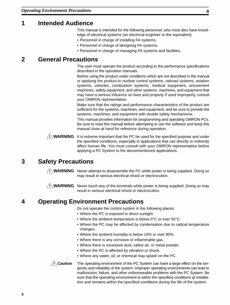
1 Intended AudienceThis manual is intended for the following personnel, who must also have knowl-edge of electrical systems (an electrical engineer or the equivalent).• Personnel in charge of installing FA systems.• Personnel in charge of designing FA systems.• Personnel in charge of managing FA systems and facilities.
2 General PrecautionsThe user must operate the product according to the performance specificationsdescribed in the operation manuals.Before using the product under conditions which are not described in the manualor applying the product to nuclear control systems, railroad systems, aviationsystems, vehicles, combustion systems, medical equipment, amusementmachines, safety equipment, and other systems, machines, and equipment thatmay have a serious influence on lives and property if used improperly, consultyour OMRON representative.Make sure that the ratings and performance characteristics of the product aresufficient for the systems, machines, and equipment, and be sure to provide thesystems, machines, and equipment with double safety mechanisms.This manual provides information for programming and operating OMRON PCs.Be sure to read this manual before attempting to use the software and keep thismanual close at hand for reference during operation.
WARNING It is extreme important that the PC be used for the specified purpose and underthe specified conditions, especially in applications that can directly or indirectlyaffect human life. You must consult with your OMRON representative beforeapplying a PC System to the abovementioned applications.
3 Safety PrecautionsWARNING Never attempt to disassemble the PC while power is being supplied. Doing so
may result in serious electrical shock or electrocution.
WARNING Never touch any of the terminals while power is being supplied. Doing so mayresult in serious electrical shock or electrocution.
4 Operating Environment PrecautionsDo not operate the control system in the following places.• Where the PC is exposed to direct sunlight.• Where the ambient temperature is below 0°C or over 55°C.• Where the PC may be affected by condensation due to radical temperature
changes.• Where the ambient humidity is below 10% or over 90%.• Where there is any corrosive or inflammable gas.• Where there is excessive dust, saline air, or metal powder.• Where the PC is affected by vibration or shock.• Where any water, oil, or chemical may splash on the PC.
Caution The operating environment of the PC System can have a large effect on the lon-gevity and reliability of the system. Improper operating environments can lead tomalfunction, failure, and other unforeseeable problems with the PC System. Besure that the operating environment is within the specified conditions at installa-tion and remains within the specified conditions during the life of the system.
Operating Environment Precautions 4

!
!
!
xi
5 Application PrecautionsObserve the following precautions when using the PC.
WARNING Failure to abide by the following precautions could lead to serious or possiblyfatal injury. Always heed these precautions.
• Always ground the system to 100 Ω or less when installing the system to pro-tect against electrical shock.
• Always turn off the power supply to the PC before attempting any of the follow-ing. Performing any of the following with the power supply turned on may leadto electrical shock:
• Assembling any devices or racks.
• Connecting or disconnecting any cables or wiring.
Caution Failure to abide by the following precautions could lead to faulty operation or thePC or the system or could damage the PC. Always heed these precautions.
• Use the PC only with the power supplies and voltages specified in the opera-tion manuals. Other power supplies and voltages may damage the PC.
• Take measures to stabilize the power supply to conform to the rated supply if itis not stable.
• Provide circuit breakers and other safety measures to provide protectionagainst shorts in external wiring.
• Do not apply voltages exceeding the rated input voltage to the input section.The input section may be destroyed.
• Do not apply voltages exceeding the maximum switching capacity to the out-put section. The output section may be destroyed.
• Always disconnect the LG terminal when performing withstand voltage tests.
• Install the PC according to instructions in the operation manuals. Improperinstallation may cause faulty operation.
• Provide proper shielding when installing in the following locations:
• Locations subject to static electricity or other sources of noise.
• Locations subject to strong electromagnetic fields.
• Locations subject to possible exposure to radiation.
• Locations near to power supply lines.
• Be sure to tighten Backplane screws, terminal screws, and cable connectorscrews securely.
• Do not attempt to take the PC apart, to repair the PC, or to modify the PC in anyway.
Caution The following precautions are necessary to ensure the general safety of the sys-tem. Always heed these precautions.
• Provide double safety mechanisms to handle incorrect signals that can begenerated by broken signal lines or momentary power interruptions.
• Provide external interlock circuits, limit circuits, and other safety circuits inaddition to any provided within the PC to ensure safety.
Application Precautions 5
1
SECTION 1Introduction
This section will introduce you to Programmable Controllers in general and specifically to the SP-series PCs and the var-ious Units available for use with them. It also describes the configurations possible with the SP-series PCs and how toconnect these configurations. Detailed wiring and installation procedures are provided in Section 2 Installation.
1-1 Features 2 . . . . . . . . . . . . . . . . . . . . . . . . . . . . . . . . . . . . . . . . . . . . . . . . . . . . . . . . . 1-2 PC Basics 2 . . . . . . . . . . . . . . . . . . . . . . . . . . . . . . . . . . . . . . . . . . . . . . . . . . . . . . . .
1-2-1 PC Terminology 3 . . . . . . . . . . . . . . . . . . . . . . . . . . . . . . . . . . . . . . . . . . 1-2-2 Overview of PC Operation 4 . . . . . . . . . . . . . . . . . . . . . . . . . . . . . . . . . .
1-3 Units 5 . . . . . . . . . . . . . . . . . . . . . . . . . . . . . . . . . . . . . . . . . . . . . . . . . . . . . . . . . . . . 1-3-1 CPU 5 . . . . . . . . . . . . . . . . . . . . . . . . . . . . . . . . . . . . . . . . . . . . . . . . . . . . 1-3-2 Programming Console 6 . . . . . . . . . . . . . . . . . . . . . . . . . . . . . . . . . . . . . . 1-3-3 Link Adapter 7 . . . . . . . . . . . . . . . . . . . . . . . . . . . . . . . . . . . . . . . . . . . . . 1-3-4 Memory Cards 7 . . . . . . . . . . . . . . . . . . . . . . . . . . . . . . . . . . . . . . . . . . . .
1-4 PC Configuration 8 . . . . . . . . . . . . . . . . . . . . . . . . . . . . . . . . . . . . . . . . . . . . . . . . . . 1-4-1 Basic Configuration 8 . . . . . . . . . . . . . . . . . . . . . . . . . . . . . . . . . . . . . . . . 1-4-2 Expanded System Configuration: PC Links 8 . . . . . . . . . . . . . . . . . . . . .
2
1-1 Features
Miniature High-performance The SP-series PCs are extremely compact yet have a programming capacityof about 100 instructions in the SP10 or about 240 instructions in the SP16and SP20. The SP10 is equipped with 34 different instructions and the SP16and SP20 are equipped with 38 instructions. With real programming capabili-ty in such a small package, these compact PCs are ideal for mounting in acontrol box or in the device being controlled.
High-speed Processing The minimum instruction execution time is as short as 0.2 microseconds. Theinput delay is only 400 microseconds.
Low Maintenance The user program is automatically transferred from RAM to EEPROM, elimi-nating the need to back up memory, which can be rewritten up to 5,000times.
Input Signal Filter To prevent errors due to chattering or external noises on input signals, theinput circuits are provided with filter timers that can be set to 0, 1, 5, or 10ms.
Efficient Distributed Control Up to four SP-series PCs can be connected with a Link Adapter. A total of128 points can be linked between the PCs, which means that up to 32 pointscan be processed by one SP-series PCs. Each PC still operates according toits own program.
Easy-to-use Analog Timers One analog timer is provided with the SP10 and two analog timers are pro-vided with the SP16 and SP20. The set time of these analog timers can bechanged even while the PC is operating, with adjustment screws located in-side the front cover.
Reversible Drum Counter A reversible drum counter can be programmed for various counter presentvalue ranges.
Step Instructions Up to five steps (four processes) of instructions can be created, making iteasy to program start-stop control.
Shift Register A 16-bit shift register can be used to control various operations easily.
Addition, subtraction, ANDs, and ORs can be performed on16-bit data.
Differentiated Instructions Up to 16 rising edge/falling edge differentiated instructions can be pro-grammed.
1-2 PC BasicsA PC (Programmable Controller) is basically a CPU (Central ProcessingUnit) containing a program and connected to input and output (I/O) devices.The program controls the PC so that when an input signal from an input de-vice turns ON, the appropriate response is made. The response normallyinvolves turning ON an output signal to some sort of output device. The inputdevices could be photoelectric sensors, pushbuttons on control panels, limitswitches, or any other device that can produce a signal that can be input intothe PC. The output devices could be solenoids, switches activating indicatorlamps, relays turning on motors, or any other devices that can be activatedby signals output from the PC.
Arithmetic/LogicalInstructions
PC Basics Section 1-2
3
For example, a sensor detecting a passing product turns ON an input to thePC. The PC responds by turning ON an output that activates a pusher thatpushes the product onto another conveyor for further processing. Anothersensor, positioned higher than the first, turns ON a different input to indicatethat the product is too tall. The PC responds by turning on another pusherpositioned before the pusher mentioned above to push the too-tall productinto a rejection box.
Although this example involves only two inputs and two outputs, it is typicalof the type of control operation that PCs can achieve. Actually even this ex-ample is much more complex than it may at first appear because of the tim-ing that would be required, i.e., “How does the PC know when to activateeach pusher?” Much more complicated operations, however, are also possi-ble. The problem is how to get the desired control signals from available in-puts at appropriate times.
To achieve proper control, the SP-series PCs use a form of PC logic calledladder-diagram programming. The next few sections will explain ladder-dia-gram programming and to prepare you to program and operate the SP-seriesPCs.
PCs historically originate in relay-based control systems. And although theintegrated circuits and internal logic of the PC have taken the place of thediscrete relays, timers, counters, and other such devices, actual PC opera-tion proceeds as if those discrete devices were still in place. PC control, how-ever, also provides computer capabilities and accuracy to achieve a greatdeal more flexibility and reliability than is possible with relays.
The symbols and other control concepts used to describe PC operation alsocome from relay-based control and form the basis of the ladder-diagram pro-gramming method. Most of the terms used to describe these symbols andconcepts, however, have come in from computer terminology.
The terminology used throughout this manual is somewhat different fromrelay terminology, but the concepts are the same. The following table showsthe relationship between relay terms and the terms used for OMRON PCs.
Relay term PC equivalent
contact input or condition
coil output or work bit
NO relay normally open condition
NC relay normally closed condition
The terms used for PC will be described in detail later.
1-2-1 PC TerminologyAlthough also provided in the Glossary at the back of this manual, the follow-ing terms are crucial to understanding PC operation and are thus explainedhere.
A device connected to the PC that sends a signal to the PC is called an in-put device ; the signal it sends is called an input signal . A signal enters thePC through terminals or through pins on a connector on a Unit. The placewhere a signal enters the PC is called an input point . This input point is allo-cated a location in memory that reflects its status, i.e., either ON or OFF. Thismemory location is called an input bit . The CPU, in its normal processingcycle, monitors the status of all input points and turns ON or OFF corre-sponding input bits accordingly.
Relay Circuits: The Rootsof PC Logic
Relay vs. PC Terminology
Inputs and Outputs
PC Basics Section 1-2
4
There are also output bits in memory that are allocated to output points onUnits through which output signals are sent to output devices , i.e., an out-put bit is turned ON to send a signal to an output device through an outputpoint. The CPU periodically turns output points ON or OFF according to thestatus of the output bits.
These terms are used when describing different aspects of PC operation.When programming, one is concerned with what information is held inmemory, and so I/O bits are referred to. When talking about the Units thatconnect the PC to the controlled system and the places on these Units wheresignals enter and leave the PC, I/O points are referred to. When wiring theseI/O points, the physical counterparts of the I/O points, either terminals or con-nector pins, are referred to. When talking about the signals that enter orleave the PC, one refers to input signals and output signals, or sometimesjust inputs and outputs. It all depends on what aspect of PC operation is be-ing talked about.
The Control System includes the PC and all I/O devices it uses to control anexternal system. A sensor that provides information to achieve control is aninput device that is clearly part of the Control System. The controlled systemis the external system that is being controlled by the PC program throughthese I/O devices. I/O devices can sometimes be considered part of the con-trolled system, e.g., a motor used to drive a conveyor belt.
1-2-2 Overview of PC OperationThe following are the basic steps involved in programming and operating theSP-series PCs. Assuming you have already purchased one or more of thesePCs, you must have a reasonable idea of the required information for stepsone and two, which are discussed briefly below. The rest of the steps are de-scribed later in this manual.
1, 2, 3.. 1. Determine what the controlled system must do, in what order, and atwhat times.
2. Determine what size of system is required, i.e.,will a single CPU sufficeor will a Link Adapter be required to join multiple CPUs.
3. On paper, assign all input and output devices to I/O points on the CPUsand determine which I/O bits will be allocated to each. (3-2 MemoryAreas)
4. Using relay ladder symbols, write a program that represents the se-quence of required operations and their inter-relationships. Be sure toalso program appropriate responses for all possible emergency situa-tions. (3-4 Basic Programming, 3-6 Advanced Programming, and 3-7Instruction Set)
5. Input the program and all required data into the PC. (3-5 Inputting theProgram)
6. Debug the program, first to eliminate any syntax errors, and then to findexecution errors.(3-8 Debugging)
7. Wire the PC to the controlled system. (Section 2 Installation)8. Test the program in an actual control situation and carry out fine tuning
as required. (Section 4 Operation)9. Record two copies of the finished program on masters and store them
safely in different locations.(3-5-8 Program Transfer)
Designing the Control System is the first step in automating any process. APC can be programmed and operated only after the overall Control System isunderstood. Designing the Control System requires, first of all, a thoroughunderstanding of the devices that are to be controlled. The first step in de-
Controlled System andControl System
Control System Design
PC Basics Section 1-2
5
signing a Control System is thus determining the requirements of the con-trolled system.
Once the entire Control System has been designed, the task of program-ming, debugging, and operation as described in the remaining sections ofthis manual can begin.
The first thing that must be assessed is the number of input and output pointsthat the controlled system will require. This is done by identifying each devicethat is to send an input signal to the PC or which is to receive an output sig-nal from the PC.
Next, determine the sequence in which control operations are to occur andthe relative timing of the operations. Identify the physical relationships be-tween the I/O devices as well as the kinds of responses that should occurbetween them.
For instance, a photoelectric switch might be functionally tied to a motor byway of a counter within the PC. When the PC receives an input from a startswitch, it could start the motor. The PC could then stop the motor when thecounter has received a specified number of input signals from the photoelec-tric switch.
Each of the related tasks must be similarly determined, from the beginning ofthe control operation to the end.
Note Programs and Peripheral Devices are not compatible between the SYSMACSP-series PCs and C-series PCs.
1-3 UnitsThis section presents the names and functions of the various components ofthe CPU, Programming Console, and Link Adapter.
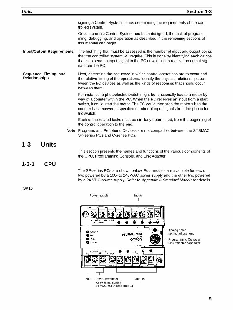
1-3-1 CPUThe SP-series PCs are shown below. Four models are available for each:two powered by a 100- to 240-VAC power supply and the other two poweredby a 24-VDC power supply. Refer to Appendix A Standard Models for details.
SP10
Power supply Inputs
Analog timersetting adjustment
Programming Console/Link Adapter connector
Power terminalsfor external supply24 VDC, 0.1 A (see note 1)
OutputsNC
Input/Output Requirements
Sequence, Timing, andRelationships
Units Section 1-3

6
SP16 and SP20 The SP20 is essentially the same as the SP16. The SP16 is shown below.
RDM(23) input(See note 3) Inputs
Analog timer 1setting adjustment
Programming Console/Link Adapter connector
Power terminalsfor external supply24 VDC, 0.2 A (see note 1)
Outputs NC
Analog timer 2setting adjustment
Power supply
Note 1. The power terminals for external supply are provided for the 100 to 240VAC model (SP__-__-A) only.
2. Connect nothing to the NC terminal.3. Input 000 is the counter input and 001 is the hard reset input for the RE-
VERSIBLE DRUM COUNTER, RDM(23). When RDM(23) isn’t beingused, these terminals can be used as normal input points but the inputsignal must be below 1 kHz.
Indicators The PC has four indicators on the front panel, POWER, RUN, LINK, and ER-ROR. The functions of the indicators are presented as follows.
POWER (green): Lit while power is supplied.RUN (green): Lit when the PC is in RUN mode and operating normally.LINK(green): Lit when the PC Link is operating normally.ERROR(red): Lights when self-diagnosis detects an error. The PC will
stop operating.
1-3-2 Programming ConsoleThe Programming Console is shown below.
Connecting cable connector
Display
Memory card access indicator
Mode switch
Memory card slot
Key pad
Units Section 1-3
!
!
7
The Programming Console is used to write and transfer programs to the PC.It is also used to monitor operation and modify data. The Programming Con-sole can be connected directly to the PC for single PCs. It can also be con-nected via a Link Adapter when PCs are connected in a PC Link configura-tion to access each PC individually without reconnection.
Note PCs connected to a Link Adapter cannot be directly connected to a Program-ming Console. The Programming Console is connected to the Link Adapter.
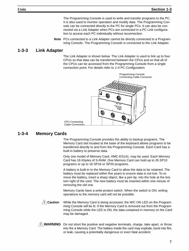
1-3-3 Link AdapterThe Link Adapter is shown below. The Link Adapter is used to link up to fourCPUs so that data can be transferred between the CPUs and so that all ofthe CPUs can be accessed from the Programming Console from a singleconnection point. For details refer to 1-4 PC Configuration.
CPU ConnectingCable Connectors
Programming Console Connecting Cable Connector
1-3-4 Memory CardsThe Programming Console provides the ability to backup programs. TheMemory Card slot located at the base of the keyboard allows programs to betransferred directly to and from the Programming Console. Each Card has abuilt-in battery to preserve data.
Only one model of Memory Card, HMC-ES141, may be used. Each MemoryCard has 16 Kbytes of S-RAM. One Memory Card can hold up to 26 SP10programs or up to 18 SP16 or SP20 programs.
A battery is built-in to the Memory Card to allow the data to be retained. Thebattery must be replaced within five years to ensure data is not lost. To re-move the battery, insert a sharp object, like a pen tip, into the hole at the bot-tom right of the card. The new battery must be inserted within one minute ofremoving the old one.
Memory Cards have a write-protect switch. When the switch is ON, writingoperations to the memory card will not be possible.
Caution While the Memory Card is being accessed, the M/C ON LED on the Program-ming Console will be lit. If the Memory Card is removed out from the Program-ming Console while the LED is ON, the data contained in memory on the Cardmay be damaged.
WARNING Do not short the positive and negative terminals, charge, take apart, or throwinto fire a Memory Card. The battery inside the card may explode, burst into fire,or leak, causing a potentially dangerous or even fatal accident.
Units Section 1-3
8
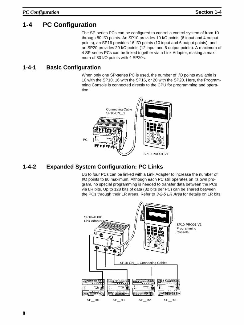
1-4 PC ConfigurationThe SP-series PCs can be configured to control a control system of from 10through 80 I/O points. An SP10 provides 10 I/O points (6 input and 4 outputpoints), an SP16 provides 16 I/O points (10 input and 6 output points), andan SP20 provides 20 I/O points (12 input and 8 output points). A maximum of4 SP-series PCs can be linked together via a Link Adapter, making a maxi-mum of 80 I/O points with 4 SP20s.
1-4-1 Basic ConfigurationWhen only one SP-series PC is used, the number of I/O points available is10 with the SP10, 16 with the SP16, or 20 with the SP20. Here, the Program-ming Console is connected directly to the CPU for programming and opera-tion.
Connecting CableSP10-CN__1
PC
SP10-PRO01-V1
1-4-2 Expanded System Configuration: PC LinksUp to four PCs can be linked with a Link Adapter to increase the number ofI/O points to 80 maximum. Although each PC still operates on its own pro-gram, no special programming is needed to transfer data between the PCsvia LR bits. Up to 128 bits of data (32 bits per PC) can be shared betweenthe PCs through their LR areas. Refer to 3-2-5 LR Area for details on LR bits.
SP10-AL001Link Adaptor
SP10-CN__1 Connecting Cables
SP10-PRO01-V1ProgrammingConsole
SP__ #0 SP__ #1 SP__ #2 SP__ #3
PC Configuration Section 1-4
9
Note 1. When two or more PCs are linked, apply power to all of the PCs at onceor to PC #0 last.
2. When using a Link Adapter, one PC must be connected to connectornumber 0 on the Link Adapter.
3. Once CPUs are connected to the Link Adapter and turned ON, unit num-bers are automatically assigned to the CPUs by the Link Adapter. Do notchange the point of connection of any CPU after a unit number has beenassigned to it. If CPUs are connected to a connecter for a different unitnumber, unpredictable errors will occur during operation.
Unit Numbers When four PCs are linked, each are given a number from 0 through 3 de-pending on which connector on the Link Adapter is used. PC #0 controls LRdata transfers between the PCs. The Programming Console is connected tothe Link Adapter and can program and monitor any of the four PCs.
PC Configuration Section 1-4

11
SECTION 2Installation
This section provides information on mounting and wiring the CPUs and on I/O specifications. Basic unit connectionsare described in 1-4 PC Configuration. Detailed specifications are provided in Appendix B Specifications.
2-1 Dimensions 12 . . . . . . . . . . . . . . . . . . . . . . . . . . . . . . . . . . . . . . . . . . . . . . . . . . . . . . . 2-2 Installation 13 . . . . . . . . . . . . . . . . . . . . . . . . . . . . . . . . . . . . . . . . . . . . . . . . . . . . . . .
2-2-1 Installation Environment 13 . . . . . . . . . . . . . . . . . . . . . . . . . . . . . . . . . . . . 2-2-2 Cooling 14 . . . . . . . . . . . . . . . . . . . . . . . . . . . . . . . . . . . . . . . . . . . . . . . . . 2-2-3 Preventing Noise 14 . . . . . . . . . . . . . . . . . . . . . . . . . . . . . . . . . . . . . . . . . . 2-2-4 Mounting Requirements 15 . . . . . . . . . . . . . . . . . . . . . . . . . . . . . . . . . . . .
2-3 Wiring 15 . . . . . . . . . . . . . . . . . . . . . . . . . . . . . . . . . . . . . . . . . . . . . . . . . . . . . . . . . . . 2-3-1 Power Supply 15 . . . . . . . . . . . . . . . . . . . . . . . . . . . . . . . . . . . . . . . . . . . . 2-3-2 I/O Connections 16 . . . . . . . . . . . . . . . . . . . . . . . . . . . . . . . . . . . . . . . . . . . 2-3-3 Precautions 20 . . . . . . . . . . . . . . . . . . . . . . . . . . . . . . . . . . . . . . . . . . . . . .
2-4 Programming Console 20 . . . . . . . . . . . . . . . . . . . . . . . . . . . . . . . . . . . . . . . . . . . . . . 2-4-1 Designating the PC 21 . . . . . . . . . . . . . . . . . . . . . . . . . . . . . . . . . . . . . . . . 2-4-2 Input Filters 22 . . . . . . . . . . . . . . . . . . . . . . . . . . . . . . . . . . . . . . . . . . . . . .
12
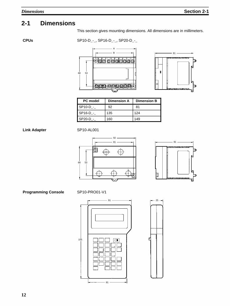
2-1 DimensionsThis section gives mounting dimensions. All dimensions are in millimeters.
SP10-D_-_, SP16-D_-_, SP20-D_-_
A
B
68 53
81
PC model Dimension A Dimension B
SP10-D_-_ 92 81
SP16-D_-_ 135 124
SP20-D_-_ 160 149
SP10-AL001
92
81
68 53
81
SP10-PRO01-V1
91
155
81
25
CPUs
Link Adapter
Programming Console
Dimensions Section 2-1
13
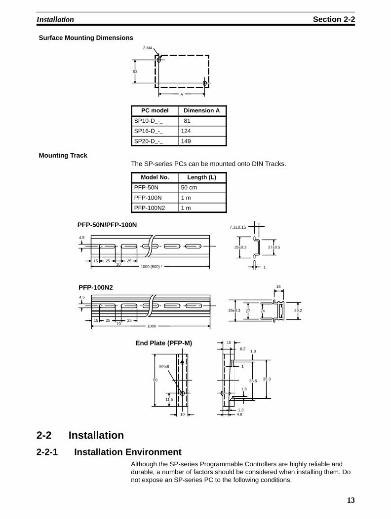
Surface Mounting Dimensions
A
2-M4
53
PC model Dimension A
SP10-D_-_ 81
SP16-D_-_ 124
SP20-D_-_ 149
Mounting TrackThe SP-series PCs can be mounted onto DIN Tracks.
Model No. Length (L)
PFP-50N 50 cm
PFP-100N 1 m
PFP-100N2 1 m
25 25
4.5
1510
1000 (500) * 1
PFP-50N/PFP-100N 7.3±0.15
35±0.3 27±0.5
25 25
4.5
1510
1000
27 24 29.2
16PFP-100N2
35±0.3
10
50
11.5
M4x8
35.335.5
1.8
1.8
1
6.2
10
4.81.3
End Plate (PFP-M)
2-2 Installation
2-2-1 Installation EnvironmentAlthough the SP-series Programmable Controllers are highly reliable anddurable, a number of factors should be considered when installing them. Donot expose an SP-series PC to the following conditions.
Installation Section 2-2
14
• An ambient temperature that falls below 0° or exceeds 55°C for the CPU, orthat falls below 0°or exceeds 45°C for the Programming Console.
• Abrupt changes in temperature that cause condensation.• A relative humidity less than 10% or greater than 90%.• Corrosive or flammable gas.• Dust, salt, or iron particles.• Direct vibration or shock.• Direct sunlight.• Splashes of water, oil, or chemicals.
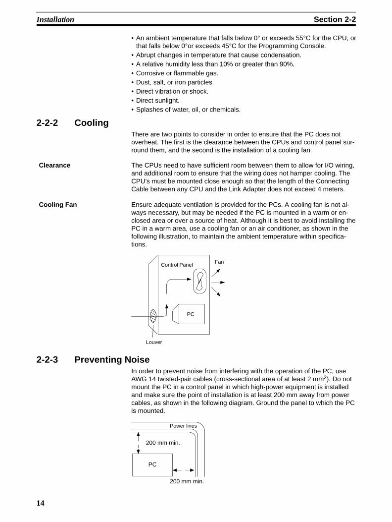
2-2-2 CoolingThere are two points to consider in order to ensure that the PC does notoverheat. The first is the clearance between the CPUs and control panel sur-round them, and the second is the installation of a cooling fan.
Clearance The CPUs need to have sufficient room between them to allow for I/O wiring,and additional room to ensure that the wiring does not hamper cooling. TheCPU’s must be mounted close enough so that the length of the ConnectingCable between any CPU and the Link Adapter does not exceed 4 meters.
Cooling Fan Ensure adequate ventilation is provided for the PCs. A cooling fan is not al-ways necessary, but may be needed if the PC is mounted in a warm or en-closed area or over a source of heat. Although it is best to avoid installing thePC in a warm area, use a cooling fan or an air conditioner, as shown in thefollowing illustration, to maintain the ambient temperature within specifica-tions.
PC
FanControl Panel
Louver
2-2-3 Preventing NoiseIn order to prevent noise from interfering with the operation of the PC, useAWG 14 twisted-pair cables (cross-sectional area of at least 2 mm2). Do notmount the PC in a control panel in which high-power equipment is installedand make sure the point of installation is at least 200 mm away from powercables, as shown in the following diagram. Ground the panel to which the PCis mounted.
PC
200 mm min.
200 mm min.
Power lines
Installation Section 2-2

15
Whenever possible, use wiring conduit to hold the I/O wiring. Standard wiringconduit should be used, and it should be long enough to completely containthe I/O wiring and keep it separated from other cables.
2-2-4 Mounting RequirementsThe system consists of from one to four CPUs and, if more than one CPU isused, a Link Adapter. The Units may be mounted horizontally or vertically, asdesired. Do not mount a Unit on its side. The Unit should be mounted withthe printing on the front panel oriented as it would normally be read. The PCcan be mounted using DIN Track or mounted directly to any sturdy supportmeeting the environmental specifications listed in Appendix B Specifications.
Track Mounting The PC may be mounted using DIN Track if desired. Use DIN Track 35 mmwide. There is a groove on the back of the Unit that is used to attach it to theDIN Track. When mounting to DIN Track, be sure to remove the mountingscrews.
RemovalMounting
Screwdriver
Engage the top hook to thetrack and push the PC in untilthe bottom hook locks onto thetrack.
Push down the bottom hookwith a screwdriver and pushthe PC upward.
Attach an End Plate to the left and right sides of the Unit to hold it in place.
SP-series PC
1010
PFP-M End PlateDIN Track DIN Track
PFP-M End Plate
DIN Track
PFP-100N (1 m)PFP-50N (0.5m)PFP-100N2 (1 m)
Note Remove the mounting screws when mounting on a track.
2-3 WiringNote Do not wire the terminal marked “NC.”
2-3-1 Power SupplyUse independent power sources for the inputs, the output loads, and the PC.Voltage fluctuations caused by current surges to motors may affect operationof the PC. When using more than one PC, use a separate power supply for
Wiring Section 2-3
16
each PC, firstly to prevent voltage drops caused by surge currents and sec-ondly, to prevent the breaker from malfunctioning.
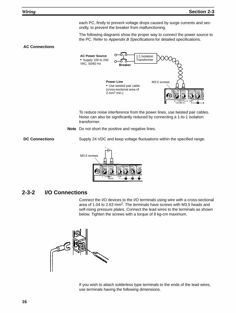
The following diagrams show the proper way to connect the power source tothe PC. Refer to Appendix B Specifications for detailed specifications.
AC Connections
AC Power Source• Supply 100 to 240VAC, 50/60 Hz
Power Line• Use twisted pair cable(cross-sectional area of2 mm2 min.)
Breaker
1:1 IsolationTransformer
M3.5 screws
To reduce noise interference from the power lines, use twisted pair cables.Noise can also be significantly reduced by connecting a 1-to-1 isolationtransformer.
Note Do not short the positive and negative lines.
DC Connections Supply 24 VDC and keep voltage fluctuations within the specified range.
+
M3.5 screws
2-3-2 I/O ConnectionsConnect the I/O devices to the I/O terminals using wire with a cross-sectionalarea of 1.04 to 2.63 mm2. The terminals have screws with M3.5 heads andself-rising pressure plates. Connect the lead wires to the terminals as shownbelow. Tighten the screws with a torque of 8 kg-cm maximum.
If you wish to attach solderless type terminals to the ends of the lead wires,use terminals having the following dimensions.
Wiring Section 2-3
17
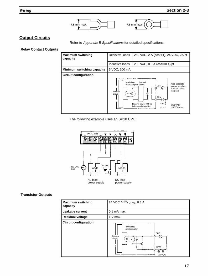
7.5 mm max.7.5 mm max.
Output CircuitsRefer to Appendix B Specifications for detailed specifications.
Relay Contact Outputs
Maximum switchingcapacity
Resistive loads 250 VAC, 2 A (cosf=1), 24 VDC, 2A/pt
Inductive loads 250 VAC, 0.5 A (cosf=0.4)/pt
Minimum switching capacity 5 VDC, 100 mA
Circuit configuration
Internalcircuit
InsulatingPhotocoupler
250 VAC, 24 VDC max.
Use seperatepower suppliesfor load powersources
Relay’s power (24 V)is internally supplied
Internal circuit
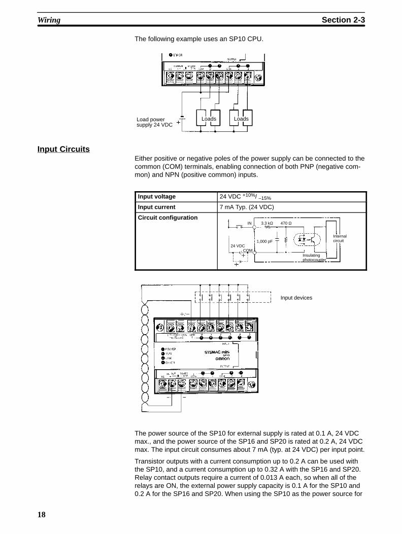
The following example uses an SP10 CPU.
250 VACmax. Loads
AC loadpower supply
DC loadpower supply
Loads24 VDC
Transistor Outputs
Maximum switchingcapacity
24 VDC +10%/ –15%, 0.3 A
Leakage current 0.1 mA max.
Residual voltage 1 V max.
Circuit configurationInsulatingphotocoupler
Internal circuit
24 VDC
Wiring Section 2-3
18
The following example uses an SP10 CPU.
Load powersupply 24 VDC
Loads Loads
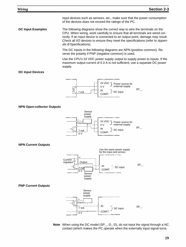
Input CircuitsEither positive or negative poles of the power supply can be connected to thecommon (COM) terminals, enabling connection of both PNP (negative com-mon) and NPN (positive common) inputs.
Input voltage 24 VDC +10%/ –15%
Input current 7 mA Typ. (24 VDC)
Circuit configuration
Insulatingphotocoupler
Internal circuit
24 VDC COM
1,000 pF
3.3 kΩ 470 ΩIN
Input devices
The power source of the SP10 for external supply is rated at 0.1 A, 24 VDCmax., and the power source of the SP16 and SP20 is rated at 0.2 A, 24 VDCmax. The input circuit consumes about 7 mA (typ. at 24 VDC) per input point.
Transistor outputs with a current consumption up to 0.2 A can be used withthe SP10, and a current consumption up to 0.32 A with the SP16 and SP20.Relay contact outputs require a current of 0.013 A each, so when all of therelays are ON, the external power supply capacity is 0.1 A for the SP10 and0.2 A for the SP16 and SP20. When using the SP10 as the power source for
Wiring Section 2-3
19
input devices such as sensors, etc., make sure that the power consumptionof the devices does not exceed the ratings of the PC.
DC Input Examples The following diagrams show the correct way to wire the terminals on theCPU. When wiring, work carefully to ensure that all terminals are wired cor-rectly. If an input device is connected to an output point, damage may result.Check all I/O devices to ensure they meet the specifications (refer to Appen-dix B Specifications).
The DC inputs in the following diagrams are NPN (positive common). Re-verse the polarity if PNP (negative common) is used.
Use the CPU’s 24 VDC power supply output to supply power to inputs. If themaximum output current of 0.3 A is not sufficient, use a separate DC powersupply.
DC Input Devices
Power source forexternal supply
DC input7 mA
24 VDC0 V
IN
COM
SP__
NPN Open-collector Outputs
Output
Sensorpowersupply
Power source forexternal supply
DC input
24 VDC0 V
INCOM
SP__7 mA0 V
NPN Current Outputs
DC inputINCOM
SP__7 mA0 V
Currentregulator Output
Sensorpowersupply
Use the same power supplyfor the input and sensor.
PNP Current Outputs
Output
Sensorpowersupply
DC inputIN
COM
SP__7 mA
0 V
Note When using the DC model (SP__-D_-D), do not input the signal through a NCcontact (which makes the PC operate when the externally input signal turns
Wiring Section 2-3

20
OFF). Proper operation for power interruptions will not be possible if NC con-tacts are used in conjunction with counter, shift, or keeping (latching) instruc-tions.
2-3-3 Precautions
Unit Sticker A sticker is provided on the upper face of the CPU to prevent foreign objects,such as wire clippings, from entering the CPU. Leave this protective stickeron until the CPU is ready for operation. The sticker must be removed beforeoperation to enable proper cooling.
Contact Outputs High inductance on for contact outputs will reduce relay life. Keep inductancelow and use an arc suppressor (such as a diode for DC loads). This is partic-ular important with inductive DC loads.
Vibration Relay operation may be adversely affected if the relay is located near contac-tors, valves, motors, or other devices that produce vibration.
Protective Circuits We recommend the use of arc suppressors to increase contact life and allevi-ate the affects of noise. Arc suppressors, however, will delay release timesomewhat and, if used incorrectly, they can inhibit proper operation. Themost common arc suppressors for AC are capacitor-resistor circuits and va-ristor circuits; for DC: capacitor-resistor circuits, diode circuits, and varistorcircuit. Do not use a capacitor without a resistor as the charging current flowto the capacitor when current is turned ON can cause the contacts to fuse.
2-4 Programming ConsoleOpen the connector cover of the PC, align the notch on the connector, andpress the connector into place.
Connection to a CPU
Connecting CableSP10-CN__1
PCSP__
SP10-PRO01-V1
Programming Console Section 2-4
21
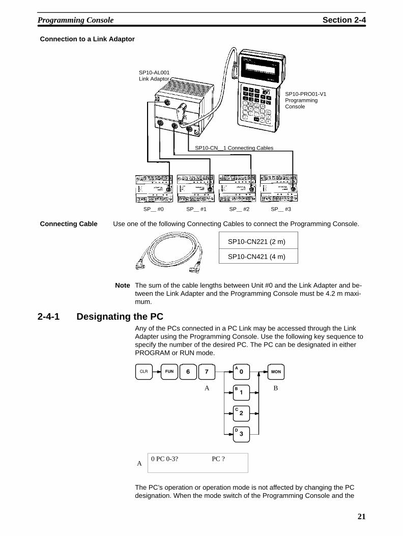
Connection to a Link Adaptor
SP10-AL001Link Adaptor
SP10-CN__1 Connecting Cables
SP10-PRO01-V1ProgrammingConsole
SP__ #0 SP__ #1 SP__ #2 SP__ #3
Connecting Cable Use one of the following Connecting Cables to connect the Programming Console.
SP10-CN221 (2 m)
SP10-CN421 (4 m)
Note The sum of the cable lengths between Unit #0 and the Link Adapter and be-tween the Link Adapter and the Programming Console must be 4.2 m maxi-mum.
2-4-1 Designating the PCAny of the PCs connected in a PC Link may be accessed through the LinkAdapter using the Programming Console. Use the following key sequence tospecify the number of the desired PC. The PC can be designated in eitherPROGRAM or RUN mode.
A B
0 PC 0-3? PC ?A
The PC’s operation or operation mode is not affected by changing the PCdesignation. When the mode switch of the Programming Console and the
Programming Console Section 2-4

22
operation mode of the PC being monitored are identical, the following mes-sage is displayed. The number in the top left corner indicates the number ofthe PC being monitored, in this case PC #1.
1-000B
When the mode switch of the Programming Console and the operation modeof the PC being monitored are not identical, the following message is dis-played.
<RUN> MODE SET ERR
B
In this example, the message indicates that the Programming Console is setto PRGM (program) mode, and that PC #1 is set to RUN mode. To clear theerror and reset the corresponding alarm, turn the Programming Consolemode to RUN and then change it back to PRGM mode. PC #1 will change toPRGM mode.
Note If there is a communication error, the display will read “COMM ERR”.
2-4-2 Input FiltersTo prevent the PC from malfunctioning due to the chattering (bouncing) of theinput device signals or induced noise, the input signals are received via afilter. The filter may be adjusted so that input pulses of a duration less than aminimum specified duration of the filter are ignored. The minimum durationbefore the detection of an input signal may be set to 0, 1, 5, or 10 ms. Thefollowing diagram illustrates the use of a filter.
External input
Input detection time
t t
The input detection time, t, for the various possible settings is given in thefollowing table. The “key” column shows which key is pressed to input eachsetting in the key sequence below.
Key Setting Actual detection time
0 0 ms t = 150 µs
1 1 ms t = 1 to 1.5 ms
2 5 ms t = 5 to 5.5 ms
3 10 ms t = 10 to 10.5 ms
During the period t to t + 0.5 ms, the positive and negative transitions of theinput signal may or may not be detected.
The filter values are set using the Programming Console. The input circuitsare grouped into three groups. The circuits included in each group depend on
Filter Value Settings
Programming Console Section 2-4
23
the PC, as shown in the table below. A different filter value can be set foreach group. The filter values can be set in PROGRAM mode only and mustbe set before operating the PC. The filter values are set simultaneously in thePC and in the Programming Console.
PC model Group 1 inputs Group 2 inputs Group 3 inputs
SP10-D_-_ 0 to 2 3 to 5 None
SP16-D_-_ 0 and 1 2 to 5 6 to 9
SP20-D_-_ 0 and 1 2 to 9 10 and 11
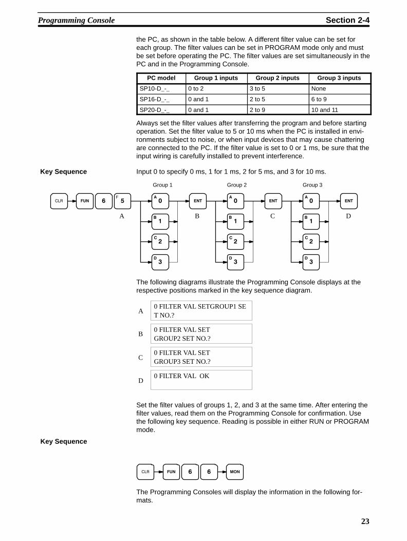
Always set the filter values after transferring the program and before startingoperation. Set the filter value to 5 or 10 ms when the PC is installed in envi-ronments subject to noise, or when input devices that may cause chatteringare connected to the PC. If the filter value is set to 0 or 1 ms, be sure that theinput wiring is carefully installed to prevent interference.
Input 0 to specify 0 ms, 1 for 1 ms, 2 for 5 ms, and 3 for 10 ms.
Group 1 Group 2
A B C
Group 3
D
The following diagrams illustrate the Programming Console displays at therespective positions marked in the key sequence diagram.
0 FILTER VAL SETGROUP1 SET NO.?
0 FILTER VAL SETGROUP2 SET NO.?
A
B
C0 FILTER VAL SETGROUP3 SET NO.?
0 FILTER VAL OKD
Set the filter values of groups 1, 2, and 3 at the same time. After entering thefilter values, read them on the Programming Console for confirmation. Usethe following key sequence. Reading is possible in either RUN or PROGRAMmode.
Key Sequence
The Programming Consoles will display the information in the following for-mats.
Key Sequence
Programming Console Section 2-4

24
SP10-PRO01
0 FILTER VAL GROUP 1-1 2-2
Group 1: 1 ms
Group 2: 5 ms
SP10-PRO01-V1The display will show the settings for groups 1 and 2 when the ProgrammingConsole is connected to an SP10.
0 PC :0-1 ProCo:0-2
PC settingsGroup 1: 0 ms; group 2: 1 ms.
Programming Console settingsGroup 1: 0 ms; group 2: 5 ms.
The display will show the settings for groups 1, 2, and 3 when the Program-ming Console is connected to an SP16 or SP20.
0 PC :0-1-2 ProCo:0-2-2
PC settingsGroup 1: 0 ms; group 2: 1 ms; group 3: 5 ms.
Programming Console settingsGroup 1: 0 ms; group 2: 5 ms; group 3: 5 ms.
Note If a pulse width of less than 150 µs is input, the SP-series CPU and the Pro-gramming Console will not work properly.
Programming Console Section 2-4

25
SECTION 3Programming
This section takes you all the way through the programming procedure from understanding memory area allocation todebugging and executing the program. Section 4 Operation will then provide procedures for monitoring PC operationand manipulating data after you have written, input, and debugged the program.
3-1 Introduction 27 . . . . . . . . . . . . . . . . . . . . . . . . . . . . . . . . . . . . . . . . . . . . . . . . . . . . . . 3-2 Memory Areas 27 . . . . . . . . . . . . . . . . . . . . . . . . . . . . . . . . . . . . . . . . . . . . . . . . . . . .
3-2-1 Data Area Structure 28 . . . . . . . . . . . . . . . . . . . . . . . . . . . . . . . . . . . . . . . . 3-2-2 I/O Bits 30 . . . . . . . . . . . . . . . . . . . . . . . . . . . . . . . . . . . . . . . . . . . . . . . . . 3-2-3 Work Bits 31 . . . . . . . . . . . . . . . . . . . . . . . . . . . . . . . . . . . . . . . . . . . . . . . . 3-2-4 Dedicated Bits 31 . . . . . . . . . . . . . . . . . . . . . . . . . . . . . . . . . . . . . . . . . . . . 3-2-5 LR Area 33 . . . . . . . . . . . . . . . . . . . . . . . . . . . . . . . . . . . . . . . . . . . . . . . . . 3-2-6 DR Area 36 . . . . . . . . . . . . . . . . . . . . . . . . . . . . . . . . . . . . . . . . . . . . . . . . . 3-2-7 TC (Timer/Counter) Area 36 . . . . . . . . . . . . . . . . . . . . . . . . . . . . . . . . . . .
3-3 The Programming Console 37 . . . . . . . . . . . . . . . . . . . . . . . . . . . . . . . . . . . . . . . . . . . 3-3-1 The Keyboard 38 . . . . . . . . . . . . . . . . . . . . . . . . . . . . . . . . . . . . . . . . . . . . 3-3-2 PC Modes 39 . . . . . . . . . . . . . . . . . . . . . . . . . . . . . . . . . . . . . . . . . . . . . . .
3-4 Basic Programming 39 . . . . . . . . . . . . . . . . . . . . . . . . . . . . . . . . . . . . . . . . . . . . . . . . 3-4-1 Terminology 39 . . . . . . . . . . . . . . . . . . . . . . . . . . . . . . . . . . . . . . . . . . . . . 3-4-2 Mnemonic Code 41 . . . . . . . . . . . . . . . . . . . . . . . . . . . . . . . . . . . . . . . . . . 3-4-3 Ladder Instructions 42 . . . . . . . . . . . . . . . . . . . . . . . . . . . . . . . . . . . . . . . . 3-4-4 OUTPUT and OUTPUT NOT 44 . . . . . . . . . . . . . . . . . . . . . . . . . . . . . . . 3-4-5 The END Instruction 44 . . . . . . . . . . . . . . . . . . . . . . . . . . . . . . . . . . . . . . . 3-4-6 Logic Block Instructions 45 . . . . . . . . . . . . . . . . . . . . . . . . . . . . . . . . . . . . 3-4-7 Coding Multiple Right-hand Instructions 51 . . . . . . . . . . . . . . . . . . . . . . .
3-5 Inputting the Program 51 . . . . . . . . . . . . . . . . . . . . . . . . . . . . . . . . . . . . . . . . . . . . . . . 3-5-1 Initial Programming Console Operation 51 . . . . . . . . . . . . . . . . . . . . . . . . 3-5-2 Designating the PC 52 . . . . . . . . . . . . . . . . . . . . . . . . . . . . . . . . . . . . . . . . 3-5-3 Clearing Memory 53 . . . . . . . . . . . . . . . . . . . . . . . . . . . . . . . . . . . . . . . . . 3-5-4 Clearing Error Messages 54 . . . . . . . . . . . . . . . . . . . . . . . . . . . . . . . . . . . . 3-5-5 Setting and Reading from Program Memory Address 54 . . . . . . . . . . . . . 3-5-6 Entering or Editing Programs 55 . . . . . . . . . . . . . . . . . . . . . . . . . . . . . . . . 3-5-7 Checking the Program 57 . . . . . . . . . . . . . . . . . . . . . . . . . . . . . . . . . . . . . . 3-5-8 Program Transfer 58 . . . . . . . . . . . . . . . . . . . . . . . . . . . . . . . . . . . . . . . . . . 3-5-9 Program Searches 61 . . . . . . . . . . . . . . . . . . . . . . . . . . . . . . . . . . . . . . . . . 3-5-10 Inserting and Deleting Instructions 61 . . . . . . . . . . . . . . . . . . . . . . . . . . . .
3-6 Advanced Programming 64 . . . . . . . . . . . . . . . . . . . . . . . . . . . . . . . . . . . . . . . . . . . . . 3-6-1 Interlocks 64 . . . . . . . . . . . . . . . . . . . . . . . . . . . . . . . . . . . . . . . . . . . . . . . . 3-6-2 Controlling Bit Status 65 . . . . . . . . . . . . . . . . . . . . . . . . . . . . . . . . . . . . . . 3-6-3 DIFFERENTIATE UP and DIFFERENTIATE DOWN 66 . . . . . . . . . . . . 3-6-4 KEEP 66 . . . . . . . . . . . . . . . . . . . . . . . . . . . . . . . . . . . . . . . . . . . . . . . . . . . 3-6-5 Self-maintaining Bits (Seal) 67 . . . . . . . . . . . . . . . . . . . . . . . . . . . . . . . . . 3-6-6 Work Bits (Internal Relays) 67 . . . . . . . . . . . . . . . . . . . . . . . . . . . . . . . . . . 3-6-7 Programming Precautions 69 . . . . . . . . . . . . . . . . . . . . . . . . . . . . . . . . . . .
26
3-7 Instruction Set 71 . . . . . . . . . . . . . . . . . . . . . . . . . . . . . . . . . . . . . . . . . . . . . . . . . . . . . 3-7-1 Notation 71 . . . . . . . . . . . . . . . . . . . . . . . . . . . . . . . . . . . . . . . . . . . . . . . . . 3-7-2 Instruction Format 71 . . . . . . . . . . . . . . . . . . . . . . . . . . . . . . . . . . . . . . . . . 3-7-3 Data Areas, Definer Values, and Flags 71 . . . . . . . . . . . . . . . . . . . . . . . . . 3-7-4 Coding Right-hand Instructions 72 . . . . . . . . . . . . . . . . . . . . . . . . . . . . . . 3-7-5 LOAD, LOAD NOT, AND, AND NOT, OR, and OR NOT 74 . . . . . . . . 3-7-6 AND LOAD and OR LOAD 75 . . . . . . . . . . . . . . . . . . . . . . . . . . . . . . . . . 3-7-7 OUTPUT and OUTPUT NOT - OUT and OUT NOT 75 . . . . . . . . . . . . . 3-7-8 DIFFERENTIATE UP and DIFFERENTIATE DOWN -
DIFU(10) and DIFD(11) 76 . . . . . . . . . . . . . . . . . . . . . . . . . . . . . . . . . . . . 3-7-9 KEEP - KEEP(12) 78 . . . . . . . . . . . . . . . . . . . . . . . . . . . . . . . . . . . . . . . . . 3-7-10 INTERLOCK and INTERLOCK CLEAR - IL(02) and ILC(03) 79 . . . . . 3-7-11 END - END(01) 81 . . . . . . . . . . . . . . . . . . . . . . . . . . . . . . . . . . . . . . . . . . 3-7-12 NO OPERATION - NOP(00) 81 . . . . . . . . . . . . . . . . . . . . . . . . . . . . . . . . 3-7-13 Timers and Counters 81 . . . . . . . . . . . . . . . . . . . . . . . . . . . . . . . . . . . . . . . 3-7-14 TIMER - TIM 83 . . . . . . . . . . . . . . . . . . . . . . . . . . . . . . . . . . . . . . . . . . . . 3-7-15 TIMER - TIMM(20) 86 . . . . . . . . . . . . . . . . . . . . . . . . . . . . . . . . . . . . . . . 3-7-16 HIGH-SPEED TIMER - TIMH(21) 87 . . . . . . . . . . . . . . . . . . . . . . . . . . . 3-7-17 ANALOG TIMER - ATIM(22) 87 . . . . . . . . . . . . . . . . . . . . . . . . . . . . . . . 3-7-18 ANALOG TIMER 1 and 2 - ATM1(25) and ATM2(26) 88 . . . . . . . . . . . 3-7-19 COUNTER - CNT 89 . . . . . . . . . . . . . . . . . . . . . . . . . . . . . . . . . . . . . . . . . 3-7-20 REVERSIBLE DRUM COUNTER -RDM(23) 92 . . . . . . . . . . . . . . . . . . 3-7-21 HIGH-SPEED COUNTER - CNTH(24) 94 . . . . . . . . . . . . . . . . . . . . . . . . 3-7-22 SHIFT REGISTER - SFT(33) 96 . . . . . . . . . . . . . . . . . . . . . . . . . . . . . . . . 3-7-23 MOVE - MOV(30) 98 . . . . . . . . . . . . . . . . . . . . . . . . . . . . . . . . . . . . . . . . 3-7-24 MOVE NOT - MVN(31) 98 . . . . . . . . . . . . . . . . . . . . . . . . . . . . . . . . . . . . 3-7-25 COMPARE - CMP(32) 99 . . . . . . . . . . . . . . . . . . . . . . . . . . . . . . . . . . . . . 3-7-26 BLOCK COMPARE - BCMP(34) 101 . . . . . . . . . . . . . . . . . . . . . . . . . . . . 3-7-27 CLEAR CARRY - CLC(44) 102 . . . . . . . . . . . . . . . . . . . . . . . . . . . . . . . . . 3-7-28 BCD ADD - ADD(40) 102 . . . . . . . . . . . . . . . . . . . . . . . . . . . . . . . . . . . . . 3-7-29 BCD SUBTRACT - SUB(41) 103 . . . . . . . . . . . . . . . . . . . . . . . . . . . . . . . . 3-7-30 AND WORD- ANDW(42) 105 . . . . . . . . . . . . . . . . . . . . . . . . . . . . . . . . . . 3-7-31 OR WORD - ORW(43) 105 . . . . . . . . . . . . . . . . . . . . . . . . . . . . . . . . . . . . . 3-7-32 STEP DEFINE and STEP START-STEP(04)/SNXT(05) 106 . . . . . . . . . . .
3-8 Debugging 109 . . . . . . . . . . . . . . . . . . . . . . . . . . . . . . . . . . . . . . . . . . . . . . . . . . . . . . . 3-8-1 Displaying and Clearing Error Messages 109 . . . . . . . . . . . . . . . . . . . . . . . 3-8-2 Reading the Scan Time 110 . . . . . . . . . . . . . . . . . . . . . . . . . . . . . . . . . . . . .
3-9 Program Execution 110 . . . . . . . . . . . . . . . . . . . . . . . . . . . . . . . . . . . . . . . . . . . . . . . . . 3-9-1 Scan 110 . . . . . . . . . . . . . . . . . . . . . . . . . . . . . . . . . . . . . . . . . . . . . . . . . . . .
3-10 I/O Response Time 111 . . . . . . . . . . . . . . . . . . . . . . . . . . . . . . . . . . . . . . . . . . . . . . . . . 3-10-1 Single PCs 112 . . . . . . . . . . . . . . . . . . . . . . . . . . . . . . . . . . . . . . . . . . . . . . . 3-10-2 Multiple PCs 113 . . . . . . . . . . . . . . . . . . . . . . . . . . . . . . . . . . . . . . . . . . . . .
27
3-1 IntroductionThere are several basic steps involved in writing a program. Sheets that canbe copied to aid in programming are provided in Appendix F I/O AssignmentSheets and Appendix G Program Coding Sheet.
1, 2, 3.. 1. Obtain a list of all I/O devices and the I/O points that have been as-signed to them and prepare a table that shows the I/O bit allocated toeach I/O device.
2. Determine what words are available for work bits and prepare a table inwhich you can allocate these as you use them.
3. Also prepare tables of TC numbers so that you can allocate these asyou use them. Remember, the function of a TC number can be definedonly once within the program. (TC numbers are described in 3-7-13 Tim-ers and Counters.)
4. Draw the ladder diagram.5. Input the program into the Programming Console.6. Check the program for syntax errors and correct these.7. Transfer the program from the Programming Console to the CPU and
execute the program to check for execution errors and correct these.8. After the entire Control System has been installed and is ready for use,
execute the program and fine tune it if required.
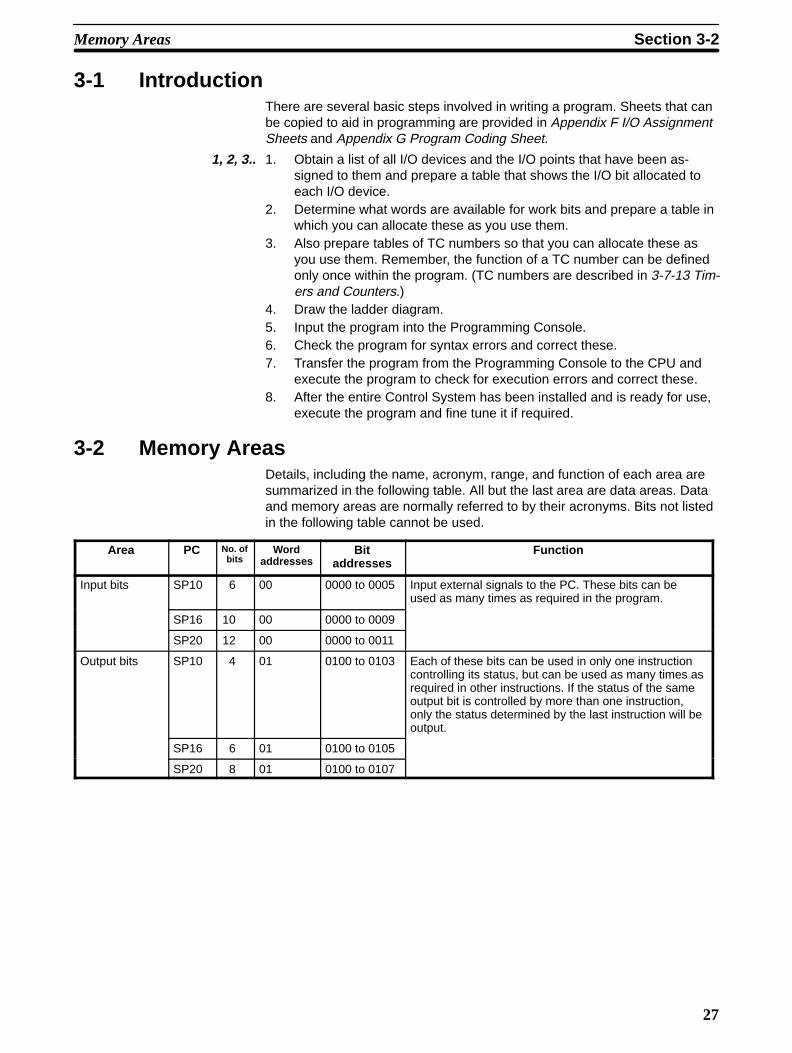
3-2 Memory AreasDetails, including the name, acronym, range, and function of each area aresummarized in the following table. All but the last area are data areas. Dataand memory areas are normally referred to by their acronyms. Bits not listedin the following table cannot be used.
Area PC No. ofbits
Wordaddresses
Bitaddresses
Function
Input bits SP10 6 00 0000 to 0005 Input external signals to the PC. These bits can beused as many times as required in the program.
SP16 10 00 0000 to 0009
SP20 12 00 0000 to 0011
Output bits SP10 4 01 0100 to 0103 Each of these bits can be used in only one instructioncontrolling its status, but can be used as many times asrequired in other instructions. If the status of the sameoutput bit is controlled by more than one instruction,only the status determined by the last instruction will beoutput.
SP16 6 01 0100 to 0105
SP20 8 01 0100 to 0107
Memory Areas Section 3-2
28
Area FunctionBitaddresses
Wordaddresses
No. ofbits
PC
Work bits SP10 36 00 0008 to 0015 These bits are used within the program to aidprogramming.
01 0104 to 0115
02 0200 to 0215
SP16 208 00 0010 to 0015
01 0106 to 0115
02 0200 to 0215
10 to 20 1000 to 2015
SP20 204 00 0012 to 0015
01 0108 to 0115
02 0200 to 0215
10 to 20 1000 to 2015
Dedicated bits SP10 20 03 0300 to 0315 These bits are assigned specific functions.
04 0408 to 0411 For details, refer to the table in 3-2-4 Dedicated Bits.
SP16, 69 03 0300 to 0315
SP20 04 0408 to 0411
05 0515
07 0700 to 0715
08 0800 to 0815
09 0900 to 0915
Data Retention(DR)
All 256max.
DR 00 toDR 15
DR 0000 toDR 1515
These bits retain their ON/OFF state even during powerinterruptions. The number of DR bits decreases if morelink bits are designated.
Link Relay(LR)
All 128max.
LR 00 toLR 07
LR 0000 to LR 0715
Used to exchange data with other SP-series PCsthrough a Link Adapter. To access the LR area, the LRarea must be defined via the Programming Console.
Timer/Counter(TC)
All 16 TIM/CNT 00 to 15 Used to define timers and counters and to accessCompletion Flags, PV, and SV for them. TC 14 is usedby the HIGH-SPEED TIMER instruction (TIMH), and TC15 is used by the ANALOG TIMER instruction.
3-2-1 Data Area StructureWhen designating a data area, the acronym for the area is always requiredfor the DR, TC, and LR areas.An actual data within any data area but the TC area is designated by its ad-dress. The address designates the bit or word within the area where the de-sired data is located. The TC area consists of TC numbers, each of which isused for a specific timer or counter defined in the program. Refer to 3-2-7 TC(Timer/Counter) Area for more details on TC numbers.
The rest of the data area consists of words, each of which consists of 16 bitsnumbered 00 through 15 from right to left. words 000 and 001 are shown be-low with bit numbers. Here, the content of each word is shown as all zeros.Bit 00 is called the rightmost bit; bit 15, the leftmost bit.
The term least significant bit is often used for rightmost bit; the term mostsignificant bit, for leftmost bit. These terms are not used in this manual be-cause a single data word is often split into two or more parts, with each partused for different parameters or operands. When this is done, the rightmostbits of a word may actually become the most significant bits, i.e., the leftmostbits in another word, when combined with other bits to form a new word.
Memory Areas Section 3-2
29
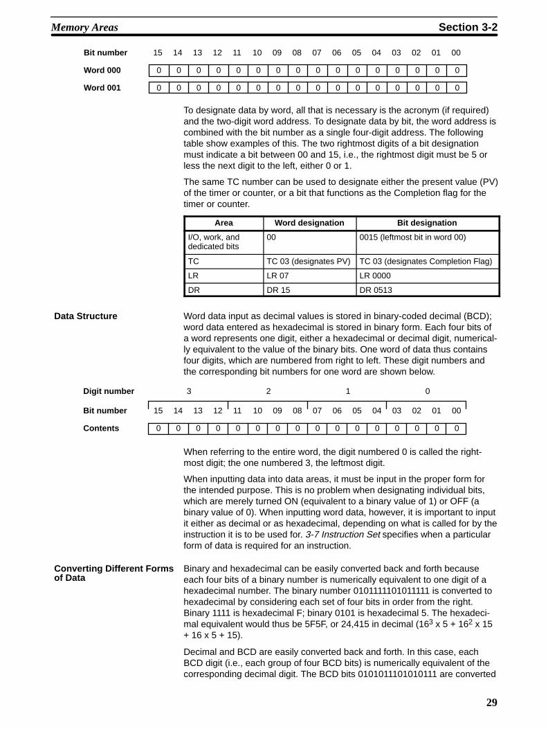
Bit number
Word 000 0 0 0 0 0 0 0 0 0 0 0 0 0 0 0 0
Word 001 0 0 0 0 0 0 0 0 0 0 0 0 0 0 0 0
15 14 13 12 11 10 09 08 07 06 05 04 03 02 01 00
To designate data by word, all that is necessary is the acronym (if required)and the two-digit word address. To designate data by bit, the word address iscombined with the bit number as a single four-digit address. The followingtable show examples of this. The two rightmost digits of a bit designationmust indicate a bit between 00 and 15, i.e., the rightmost digit must be 5 orless the next digit to the left, either 0 or 1.
The same TC number can be used to designate either the present value (PV)of the timer or counter, or a bit that functions as the Completion flag for thetimer or counter.
Area Word designation Bit designation
I/O, work, anddedicated bits
00 0015 (leftmost bit in word 00)
TC TC 03 (designates PV) TC 03 (designates Completion Flag)
LR LR 07 LR 0000
DR DR 15 DR 0513
Word data input as decimal values is stored in binary-coded decimal (BCD);word data entered as hexadecimal is stored in binary form. Each four bits ofa word represents one digit, either a hexadecimal or decimal digit, numerical-ly equivalent to the value of the binary bits. One word of data thus containsfour digits, which are numbered from right to left. These digit numbers andthe corresponding bit numbers for one word are shown below.
Bit number
Contents 0 0 0 0 0 0 0 0 0 0 0 0 0 0 0 0
15 14 13 12 11 10 09 08 07 06 05 04 03 02 01 00
Digit number 3 2 1 0
When referring to the entire word, the digit numbered 0 is called the right-most digit; the one numbered 3, the leftmost digit.
When inputting data into data areas, it must be input in the proper form forthe intended purpose. This is no problem when designating individual bits,which are merely turned ON (equivalent to a binary value of 1) or OFF (abinary value of 0). When inputting word data, however, it is important to inputit either as decimal or as hexadecimal, depending on what is called for by theinstruction it is to be used for. 3-7 Instruction Set specifies when a particularform of data is required for an instruction.
Binary and hexadecimal can be easily converted back and forth becauseeach four bits of a binary number is numerically equivalent to one digit of ahexadecimal number. The binary number 0101111101011111 is converted tohexadecimal by considering each set of four bits in order from the right.Binary 1111 is hexadecimal F; binary 0101 is hexadecimal 5. The hexadeci-mal equivalent would thus be 5F5F, or 24,415 in decimal (163 x 5 + 162 x 15+ 16 x 5 + 15).
Decimal and BCD are easily converted back and forth. In this case, eachBCD digit (i.e., each group of four BCD bits) is numerically equivalent of thecorresponding decimal digit. The BCD bits 0101011101010111 are converted
Data Structure
Converting Different Formsof Data
Memory Areas Section 3-2

30
to decimal by considering each four bits from the right. Binary 0101 is deci-mal 5; binary 0111 is decimal 7. The decimal equivalent would thus be 5,757.Note that this is not the same numeric value as the hexadecimal equivalentof 0101011101010111, which would be 5,757 hexadecimal, or 22,359 in deci-mal (163 x 5 + 162 x 7 + 16 x 5 + 7).
Because the numeric equivalent of each four BCD binary bits must be nu-merically equivalent to a decimal value, any four bit combination numericallygreater then 9 cannot be used, e.g., 1011 is not allowed because it is numeri-cally equivalent to 11, which cannot be expressed as a single digit in decimalnotation. The binary bits 1011 are of course allowed in hexadecimal are aequivalent to the hexadecimal digit C.
Decimal points are used in timers only. The least significant digit representstenths of a second. All arithmetic instructions operate on integers only.
Normally, when the content of a data area word is specified for an instruction,the instruction is performed directly on the content of that word. For example,suppose CMP(32) (COMPARE), with word 05 as the first operand and DR 10as the second operand, is used in the program. When this instruction is ex-ecuted, the content of word 05 is compared with that of DR 10.
It is also possible, however, to use indirect DR addresses as operands forinstructions. If *DR 01 is specified as the data for a programming instruction,the asterisk in front of DR indicates that it is an indirect address that specifiesanother DR word which contains the actual operand data. If, in this case, thecontent of DR 01 is 06, then *DR 01 indicates DR 06 as the word that con-tains the desired data, and the content of DR 06 is used as the operand inthe instruction. The following example shows this type of indirect addressingwith the MOVE instruction (MOV(30)).
MOV(30)
*DR 01
LR 00
Word ContentDR 00 4C01DR 01 0006DR 02 F693
DR 06 5555DR 07 21A5DR 08 D945
5555moved toLR 00.
Indicates DR 06.
Indirect address
3-2-2 I/O Bits
Input bits are used to read the status of input terminals, i.e., input bits areused as operands in the program to control program execution. Output bitsare used to control the status of output terminals, i.e., various conditions inthe program are used to determine the status of output bits through the OUT-PUT and other instructions. The relationship of the I/O bits and terminals inthe SP10 is shown below. The relationship between I/O bits and terminals inthe SP16 and SP20 follows the same pattern.
Decimal Points
Indirect Addressing
Memory Areas Section 3-2
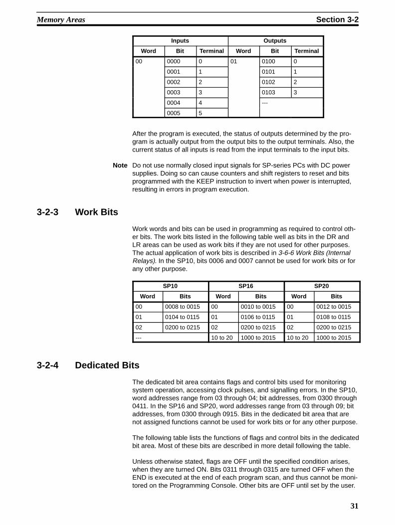
31
Inputs Outputs
Word Bit Terminal Word Bit Terminal
00 0000 0 01 0100 0
0001 1 0101 1
0002 2 0102 2
0003 3 0103 3
0004 4 ---
0005 5
After the program is executed, the status of outputs determined by the pro-gram is actually output from the output bits to the output terminals. Also, thecurrent status of all inputs is read from the input terminals to the input bits.
Note Do not use normally closed input signals for SP-series PCs with DC powersupplies. Doing so can cause counters and shift registers to reset and bitsprogrammed with the KEEP instruction to invert when power is interrupted,resulting in errors in program execution.
3-2-3 Work Bits
Work words and bits can be used in programming as required to control oth-er bits. The work bits listed in the following table well as bits in the DR andLR areas can be used as work bits if they are not used for other purposes.The actual application of work bits is described in 3-6-6 Work Bits (InternalRelays). In the SP10, bits 0006 and 0007 cannot be used for work bits or forany other purpose.
SP10 SP16 SP20
Word Bits Word Bits Word Bits
00 0008 to 0015 00 0010 to 0015 00 0012 to 0015
01 0104 to 0115 01 0106 to 0115 01 0108 to 0115
02 0200 to 0215 02 0200 to 0215 02 0200 to 0215
--- 10 to 20 1000 to 2015 10 to 20 1000 to 2015
3-2-4 Dedicated Bits
The dedicated bit area contains flags and control bits used for monitoringsystem operation, accessing clock pulses, and signalling errors. In the SP10,word addresses range from 03 through 04; bit addresses, from 0300 through0411. In the SP16 and SP20, word addresses range from 03 through 09; bitaddresses, from 0300 through 0915. Bits in the dedicated bit area that arenot assigned functions cannot be used for work bits or for any other purpose.
The following table lists the functions of flags and control bits in the dedicatedbit area. Most of these bits are described in more detail following the table.
Unless otherwise stated, flags are OFF until the specified condition arises,when they are turned ON. Bits 0311 through 0315 are turned OFF when theEND is executed at the end of each program scan, and thus cannot be moni-tored on the Programming Console. Other bits are OFF until set by the user.
Memory Areas Section 3-2
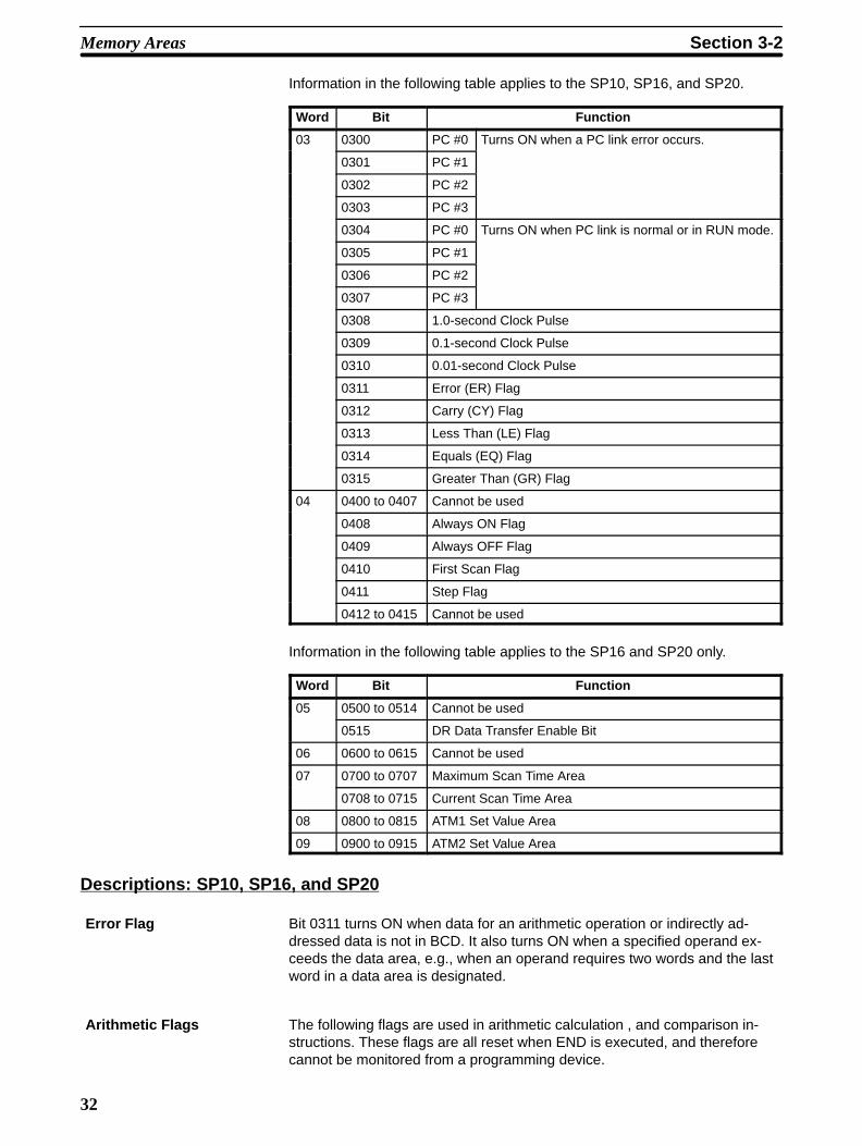
32
Information in the following table applies to the SP10, SP16, and SP20.
Word Bit Function
03 0300 PC #0 Turns ON when a PC link error occurs.
0301 PC #1
0302 PC #2
0303 PC #3
0304 PC #0 Turns ON when PC link is normal or in RUN mode.
0305 PC #1
0306 PC #2
0307 PC #3
0308 1.0-second Clock Pulse
0309 0.1-second Clock Pulse
0310 0.01-second Clock Pulse
0311 Error (ER) Flag
0312 Carry (CY) Flag
0313 Less Than (LE) Flag
0314 Equals (EQ) Flag
0315 Greater Than (GR) Flag
04 0400 to 0407 Cannot be used
0408 Always ON Flag
0409 Always OFF Flag
0410 First Scan Flag
0411 Step Flag
0412 to 0415 Cannot be used
Information in the following table applies to the SP16 and SP20 only.
Word Bit Function
05 0500 to 0514 Cannot be used
0515 DR Data Transfer Enable Bit
06 0600 to 0615 Cannot be used
07 0700 to 0707 Maximum Scan Time Area
0708 to 0715 Current Scan Time Area
08 0800 to 0815 ATM1 Set Value Area
09 0900 to 0915 ATM2 Set Value Area
Descriptions: SP10, SP16, and SP20
Error Flag Bit 0311 turns ON when data for an arithmetic operation or indirectly ad-dressed data is not in BCD. It also turns ON when a specified operand ex-ceeds the data area, e.g., when an operand requires two words and the lastword in a data area is designated.
Arithmetic Flags The following flags are used in arithmetic calculation , and comparison in-structions. These flags are all reset when END is executed, and thereforecannot be monitored from a programming device.
Memory Areas Section 3-2
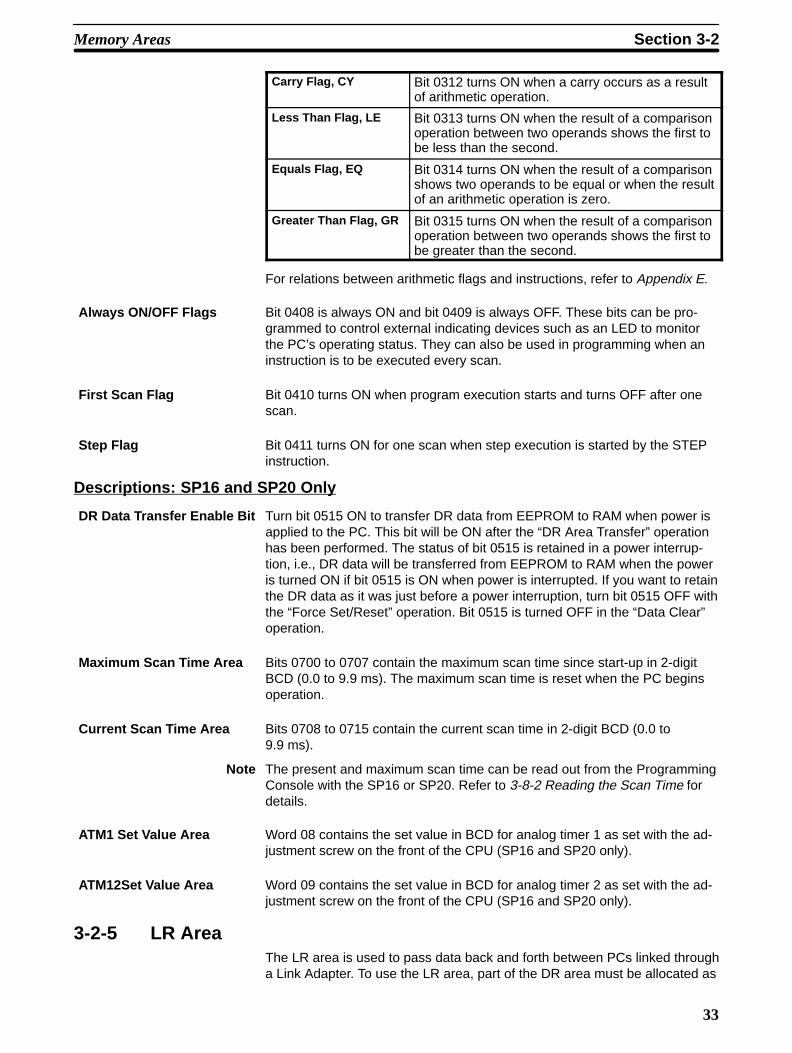
33
Carry Flag, CY Bit 0312 turns ON when a carry occurs as a resultof arithmetic operation.
Less Than Flag, LE Bit 0313 turns ON when the result of a comparisonoperation between two operands shows the first tobe less than the second.
Equals Flag, EQ Bit 0314 turns ON when the result of a comparisonshows two operands to be equal or when the resultof an arithmetic operation is zero.
Greater Than Flag, GR Bit 0315 turns ON when the result of a comparisonoperation between two operands shows the first tobe greater than the second.
For relations between arithmetic flags and instructions, refer to Appendix E.
Always ON/OFF Flags Bit 0408 is always ON and bit 0409 is always OFF. These bits can be pro-grammed to control external indicating devices such as an LED to monitorthe PC’s operating status. They can also be used in programming when aninstruction is to be executed every scan.
First Scan Flag Bit 0410 turns ON when program execution starts and turns OFF after onescan.
Step Flag Bit 0411 turns ON for one scan when step execution is started by the STEPinstruction.
Descriptions: SP16 and SP20 Only
DR Data Transfer Enable Bit Turn bit 0515 ON to transfer DR data from EEPROM to RAM when power isapplied to the PC. This bit will be ON after the “DR Area Transfer” operationhas been performed. The status of bit 0515 is retained in a power interrup-tion, i.e., DR data will be transferred from EEPROM to RAM when the poweris turned ON if bit 0515 is ON when power is interrupted. If you want to retainthe DR data as it was just before a power interruption, turn bit 0515 OFF withthe “Force Set/Reset” operation. Bit 0515 is turned OFF in the “Data Clear”operation.
Maximum Scan Time Area Bits 0700 to 0707 contain the maximum scan time since start-up in 2-digitBCD (0.0 to 9.9 ms). The maximum scan time is reset when the PC beginsoperation.
Current Scan Time Area Bits 0708 to 0715 contain the current scan time in 2-digit BCD (0.0 to9.9 ms).
Note The present and maximum scan time can be read out from the ProgrammingConsole with the SP16 or SP20. Refer to 3-8-2 Reading the Scan Time fordetails.
ATM1 Set Value Area Word 08 contains the set value in BCD for analog timer 1 as set with the ad-justment screw on the front of the CPU (SP16 and SP20 only).
ATM12Set Value Area Word 09 contains the set value in BCD for analog timer 2 as set with the ad-justment screw on the front of the CPU (SP16 and SP20 only).
3-2-5 LR AreaThe LR area is used to pass data back and forth between PCs linked througha Link Adapter. To use the LR area, part of the DR area must be allocated as
Memory Areas Section 3-2
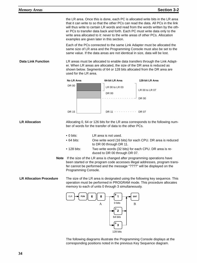
34
the LR area. Once this is done, each PC is allocated write bits in the LR areathat it can write to so that the other PCs can read the data. All PCs in the linkwill thus write to certain LR words and read from the words written by the oth-er PCs to transfer data back and forth. Each PC must write data only to thewrite area allocated to it: never to the write areas of other PCs. Allocationexamples are given later in this section.
Each of the PCs connected to the same Link Adapter must be allocated thesame size of LR area and the Programming Console must also be set to thesame value. If the data areas are not identical in size, data will be lost.
LR areas must be allocated to enable data transfers through the Link Adapt-er. When LR areas are allocated, the size of the DR area is reduced asshown below. Segments of 64 or 128 bits allocated from the DR area areused for the LR area.
DR 00
DR 15
DR 00
DR 11
LR 00 to LR 03LR 00 to LR 07
DR 00
DR 07
No LR Area 64-bit LR Area 128-bit LR Area
Allocating 0, 64 or 126 bits for the LR area corresponds to the following num-ber of words for the transfer of data to the other PCs.
• 0 bits: LR area is not used.• 64 bits: One write word (16 bits) for each CPU. DR area is reduced
to DR 00 through DR 11.• 128 bits: Two write words (32 bits) for each CPU. DR area is re-
duced to DR 00 through DR 07.
Note If the size of the LR area is changed after programming operations havebeen started or the program code accesses illegal addresses, program trans-fer cannot be performed and the message “????” will be displayed on theProgramming Console.
The size of the LR area is designated using the following key sequence. Thisoperation must be performed in PROGRAM mode. This procedure allocatesmemory to each of units 0 through 3 simultaneously.
0 bits
64 bits
128 bits
A B
The following diagrams illustrate the Programming Console displays at thecorresponding positions noted in the previous Key Sequence diagram.
Data Link Function
LR Allocation
LR Allocation Procedure
Memory Areas Section 3-2
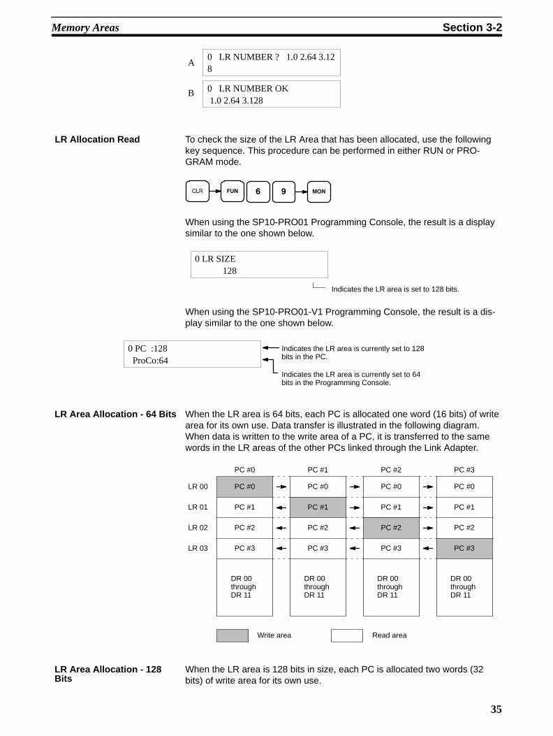
35
0 LR NUMBER ? 1.0 2.64 3.128
0 LR NUMBER OK 1.0 2.64 3.128
A
B
LR Allocation Read To check the size of the LR Area that has been allocated, use the followingkey sequence. This procedure can be performed in either RUN or PRO-GRAM mode.
When using the SP10-PRO01 Programming Console, the result is a displaysimilar to the one shown below.
0 LR SIZE 128
Indicates the LR area is set to 128 bits.
When using the SP10-PRO01-V1 Programming Console, the result is a dis-play similar to the one shown below.
0 PC :128 ProCo:64
Indicates the LR area is currently set to 128bits in the PC.
Indicates the LR area is currently set to 64bits in the Programming Console.
When the LR area is 64 bits, each PC is allocated one word (16 bits) of writearea for its own use. Data transfer is illustrated in the following diagram.When data is written to the write area of a PC, it is transferred to the samewords in the LR areas of the other PCs linked through the Link Adapter.
PC #0
PC #0
PC #1
PC #2
PC #3
DR 00throughDR 11
PC #1
PC #0
PC #1
PC #2
PC #3
DR 00throughDR 11
PC #2
PC #0
PC #1
PC #2
PC #3
DR 00throughDR 11
PC #3
PC #0
PC #1
PC #2
PC #3
DR 00throughDR 11
LR 00
LR 01
LR 02
LR 03
Write area Read area
When the LR area is 128 bits in size, each PC is allocated two words (32bits) of write area for its own use.
LR Area Allocation - 64 Bits
LR Area Allocation - 128Bits
Memory Areas Section 3-2
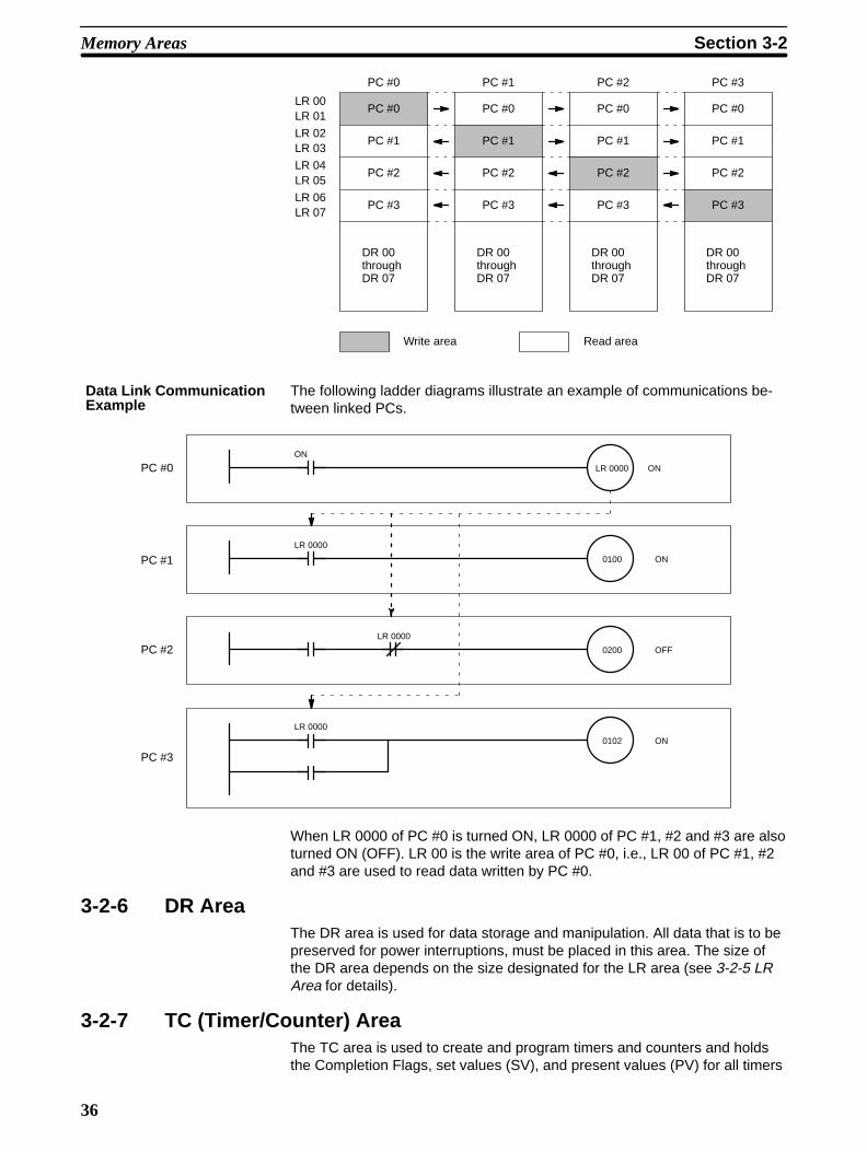
36
PC #0
PC #0
PC #1
PC #2
PC #3
DR 00throughDR 07
PC #1
PC #0
PC #1
PC #2
PC #3
DR 00throughDR 07
PC #2
PC #0
PC #1
PC #2
PC #3
DR 00throughDR 07
PC #3
PC #0
PC #1
PC #2
PC #3
DR 00throughDR 07
LR 00LR 01
LR 02LR 03
LR 04LR 05
LR 06LR 07
Write area Read area
The following ladder diagrams illustrate an example of communications be-tween linked PCs.
ON
LR 0000
LR 0000 ON
LR 0000
0100 ON
0200 OFF
LR 0000
0102 ON
PC #0
PC #1
PC #2
PC #3
When LR 0000 of PC #0 is turned ON, LR 0000 of PC #1, #2 and #3 are alsoturned ON (OFF). LR 00 is the write area of PC #0, i.e., LR 00 of PC #1, #2and #3 are used to read data written by PC #0.
3-2-6 DR AreaThe DR area is used for data storage and manipulation. All data that is to bepreserved for power interruptions, must be placed in this area. The size ofthe DR area depends on the size designated for the LR area (see 3-2-5 LRArea for details).
3-2-7 TC (Timer/Counter) Area The TC area is used to create and program timers and counters and holdsthe Completion Flags, set values (SV), and present values (PV) for all timers
Data Link CommunicationExample
Memory Areas Section 3-2
37
and counters. All of these are accessed through TC numbers ranging fromTC 00 through TC 15. Each TC number is defined as either a timer or count-er using one of the following instructions: TIM, TIMM(20), TIMH(21),ATIM(22), ATM1(25), ATM2(26), CNT, RDM(23), or CNTH(24). No prefix isrequired when using a TC number as a definer in a timer or counter instruc-tion.
Once a TC number has been defined using one of these instructions, it can-not be redefined elsewhere in the program either using the same or a differ-ent instruction. If the same TC number is defined in more than one of theseinstructions or in the same instruction twice, an error will be generated. Thereare no restrictions on the order in which TC numbers can be used. TC num-bers TC 11 through TC 15 (just TC 14 and TC 15 for the SP10) are assignedto specific instructions, as shown in the table below.
TC number Instruction Applicable PCs
TC 11 ANALOG TIMER 1, ATM1(25) SP16, SP20
TC 12 ANALOG TIMER 2, ATM2(26) SP16, SP20
TC 13 HIGH-SPEED COUNTER, CNTH(24) SP16, SP20
TC 14 HIGH-SPEED TIMER, TIMH(21) SP10, SP16, SP20
TC 15 ANALOG TIMER, ATIM(22) SP10, SP16, SP20
Once defined, a TC number can be designated as an operand in one or moreof certain instructions other than those listed above and can be used asmany times as necessary in ladder instructions. When defined as a timer, aTC number designated as an operand takes a TIM prefix. The TIM prefix isused regardless of the timer instruction that was used to define the timer.Once defined as a counter, the TC number designated as an operand takesa CNT prefix. The CNT is also used regardless of the counter instruction thatwas used to define the counter.
TC numbers can be designated for operands that require bit data or for oper-ands that require word data. When designated as an operand that requiresbit data, the TC number accesses the Completion Flag of the timer or count-er. When designated as an operand that requires word data, the TC numberaccesses a memory location that holds the PV of the timer or counter.
The TC area retains the SVs of both timers and counters during power inter-ruptions. The PVs of timers are reset when PC operation is begun and whenreset in interlocked program sections. Refer to 3-7-10 Interlock and InterlockClear - IL(02) and ILC(03) for details on timer and counter operation in inter-locked program sections. The PVs of counters are not reset at these times.
Note that in programming “TIM 0” is used to designate three things: the Timerinstruction defined with TC number 00, the Completion Flag for this timer,and the PV of this timer. The meaning in context should be clear, i.e., the firstis always an instruction, the second is always a bit, and the third is always aword. The same is true of all other TC numbers prefixed with TIM or CNT.
3-3 The Programming ConsoleThe Programming Console is used to program, monitor, and maintain thePCs. All programming is first input into the Programming Console and thentransferred to the CPUs for execution or Memory Cards for storage.
The Programming Console keys are divided into several sections for ease inoperation. The gray keys are used in combination with the white numerickeys to designate instructions, operands, and Programming Console func-tions. The yellow keys are used to designate Programming Console opera-
The Programming Console Section 3-3

38
tions. The red Clear Key is used to clear the display and cancel Program-ming Console operations. Key functions are described in detail in the nextsection.
3-3-1 The Keyboard
Key Function
FUNFunction Key Designates instructions via function codes or designates Programming Console
functions.
NOTNOT Key Pressed after the Load, AND, or OR Key to designate a normally closed
condition with the LOAD, AND, or OR instructions.
SHIFTShift Key Designates the upper function on keys that have two functions. Used with the
CH/* Key, the Bit/Constant Key, or Numeric Keys 0 through 5.
ANDAND Key Inputs an AND instruction.
OROR Key Inputs an OR instruction.
LDLoad Key Inputs a LOAD instruction when pressed alone or an OR LOAD or AND LOAD
instruction when pressed after the OR or AND Key.
OUTOutput Key Inputs an OUTPUT instruction when pressed alone or an OUTPUT NOT
instruction if pressed before the NOT key.
TIMTimer Key Inputs a TIMER instruction.
CNTCounter Key Inputs a COUNTER instruction.
LRLink Bit Key Indicates an LR (link) bit.
DRData Bit Key Indicates a DR (data) bit.
CH
*Word/IndirectAddress Key
Indicates an indirect DR address when pressed without the Shift Key anddesignates a word address when pressed after the Shift Key.
CONT#
Bit/Constant Key Indicates a bit or a constant depending on whether the Shift Key is used.
CHGChange Key Pressed to change the content of a memory address.
DELDelete Key Pressed to delete an instruction in combination with the Up Key.
INSInsert Key Pressed to insert an instruction in combination with the Down Key.
CLRClear Key Normally cancels operations and resets the Programming Console.
ENTEnter Key Inputs instructions, set values, and other data.
Up Key Pressed when reading programs to scroll the program memory address orpressed to delete instructions (see Delete Key).
Down Key Pressed when reading programs to scroll the program memory address orpressed to insert instructions (see Insert Key).
MONMonitor Key Pressed to monitor bit status or word content.
to
to
Numeric keys Input numeric values, addresses, and other data. The Shift key is pressedbefore the 0 through 5 Keys to input hexadecimal numerals A through F.
The Programming Console Section 3-3

!
!
39
3-3-2 PC ModesThere are two PC operating modes that are set from the Programming Con-sole: RUN and PROGRAM.
RUN mode is used for normal program execution once the program hasbeen input. In RUN mode, input terminal status is read into the PC and out-put terminals are updated according to program execution results.
PROGRAM mode is used for programming operations to input and debug theprogram when setting up the control system and for data access and manip-ulation once a control system is running. The program is not executed inPROGRAM mode.
When the PC is turned on with the Programming Console attached, themode switch on the Programming Console will determine the initial operatingmode.
If the Programming Console is not attached, the PC will always start in RUNmode and the program will be executed immediately.
If the Programming Console is attached after the PC is already turned on, thecurrent mode will continue regardless of the setting of the Programming Con-sole mode switch.
WARNING Always confirm that the Programming Console is in PROGRAM mode whenturning on the PC with a Programming Console connected unless another modeis desired for a specific purpose. If the Programming Console is in RUN modewhen PC power is turned on, any program in Program Memory will be executed,possibly causing a PC-controlled system to begin operation. If the START inputon the CPU Power Supply Unit is ON and there is no device connected to theCPU, ensure that commencing operation is safe and appropriate before turningon the PC.
WARNING Do not leave the Programming Console connected to the PC by an extensioncable when in RUN mode. Noise detected via the extension cable can enter thePC, affecting the program and thus the controlled system.
3-4 Basic Programming
3-4-1 TerminologyThere are basically two types of instructions used in ladder-diagram pro-gramming: ladder instructions that correspond to the conditions on the ladderdiagram and right-hand instructions that are used on the right side of the lad-der diagram and are controlled by the ladder instructions. Ladder instructionsare used in instruction form only when converting a program to mnemoniccode.
Most instructions have at least one or more operands associated with them.Operands indicate or provide the data on which an instruction is to be per-formed. These are sometimes input as the actual numeric values, but areusually the addresses of words or bits that contain the data to be used. Forinstance, a MOVE instruction that has word 00 designated as the source op-erand will move the contents of word 00 to some other location. The otherlocation is also designated as an operand. A bit whose address is designatedas an operand is called an operand bit; a word whose address is designatedas an operand is called an operand word. If the actual value is entered as aconstant, it is preceded by # to indicate that it is not an address.
Startup Mode
Basic Programming Section 3-4
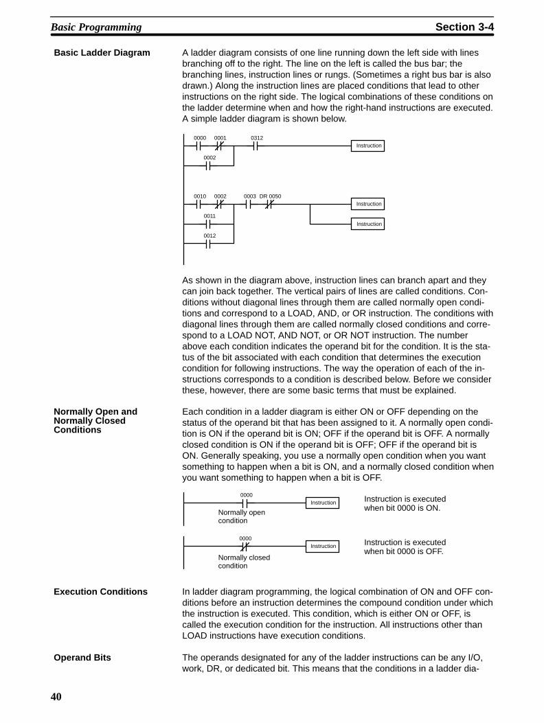
40
Basic Ladder Diagram A ladder diagram consists of one line running down the left side with linesbranching off to the right. The line on the left is called the bus bar; thebranching lines, instruction lines or rungs. (Sometimes a right bus bar is alsodrawn.) Along the instruction lines are placed conditions that lead to otherinstructions on the right side. The logical combinations of these conditions onthe ladder determine when and how the right-hand instructions are executed.A simple ladder diagram is shown below.
0000 0001
Instruction
Instruction
0002
0312
0010 0002
0011
0012
0003 DR 0050
Instruction
As shown in the diagram above, instruction lines can branch apart and theycan join back together. The vertical pairs of lines are called conditions. Con-ditions without diagonal lines through them are called normally open condi-tions and correspond to a LOAD, AND, or OR instruction. The conditions withdiagonal lines through them are called normally closed conditions and corre-spond to a LOAD NOT, AND NOT, or OR NOT instruction. The numberabove each condition indicates the operand bit for the condition. It is the sta-tus of the bit associated with each condition that determines the executioncondition for following instructions. The way the operation of each of the in-structions corresponds to a condition is described below. Before we considerthese, however, there are some basic terms that must be explained.
Each condition in a ladder diagram is either ON or OFF depending on thestatus of the operand bit that has been assigned to it. A normally open condi-tion is ON if the operand bit is ON; OFF if the operand bit is OFF. A normallyclosed condition is ON if the operand bit is OFF; OFF if the operand bit isON. Generally speaking, you use a normally open condition when you wantsomething to happen when a bit is ON, and a normally closed condition whenyou want something to happen when a bit is OFF.
Instruction
Instruction
0000
0000Instruction is executedwhen bit 0000 is ON.
Instruction is executedwhen bit 0000 is OFF.
Normally opencondition
Normally closedcondition
In ladder diagram programming, the logical combination of ON and OFF con-ditions before an instruction determines the compound condition under whichthe instruction is executed. This condition, which is either ON or OFF, iscalled the execution condition for the instruction. All instructions other thanLOAD instructions have execution conditions.
The operands designated for any of the ladder instructions can be any I/O,work, DR, or dedicated bit. This means that the conditions in a ladder dia-
Normally Open andNormally ClosedConditions
Execution Conditions
Operand Bits
Basic Programming Section 3-4
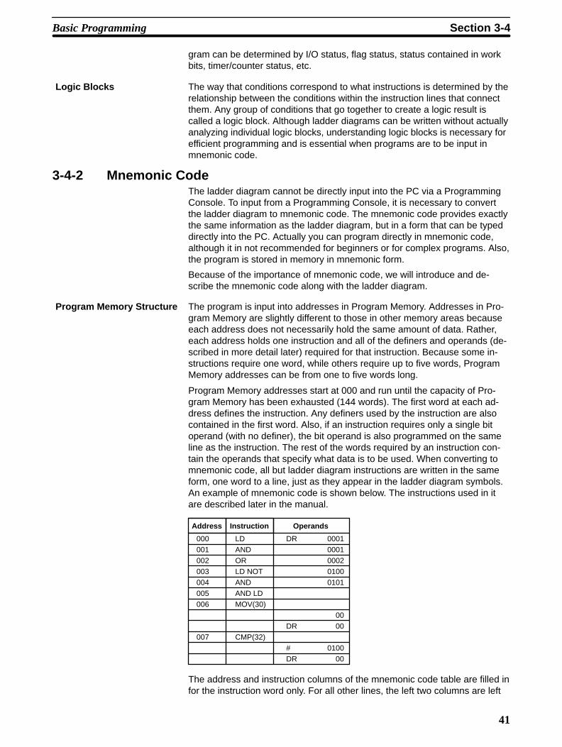
41
gram can be determined by I/O status, flag status, status contained in workbits, timer/counter status, etc.
The way that conditions correspond to what instructions is determined by therelationship between the conditions within the instruction lines that connectthem. Any group of conditions that go together to create a logic result iscalled a logic block. Although ladder diagrams can be written without actuallyanalyzing individual logic blocks, understanding logic blocks is necessary forefficient programming and is essential when programs are to be input inmnemonic code.
3-4-2 Mnemonic CodeThe ladder diagram cannot be directly input into the PC via a ProgrammingConsole. To input from a Programming Console, it is necessary to convertthe ladder diagram to mnemonic code. The mnemonic code provides exactlythe same information as the ladder diagram, but in a form that can be typeddirectly into the PC. Actually you can program directly in mnemonic code,although it in not recommended for beginners or for complex programs. Also,the program is stored in memory in mnemonic form.
Because of the importance of mnemonic code, we will introduce and de-scribe the mnemonic code along with the ladder diagram.
The program is input into addresses in Program Memory. Addresses in Pro-gram Memory are slightly different to those in other memory areas becauseeach address does not necessarily hold the same amount of data. Rather,each address holds one instruction and all of the definers and operands (de-scribed in more detail later) required for that instruction. Because some in-structions require one word, while others require up to five words, ProgramMemory addresses can be from one to five words long.
Program Memory addresses start at 000 and run until the capacity of Pro-gram Memory has been exhausted (144 words). The first word at each ad-dress defines the instruction. Any definers used by the instruction are alsocontained in the first word. Also, if an instruction requires only a single bitoperand (with no definer), the bit operand is also programmed on the sameline as the instruction. The rest of the words required by an instruction con-tain the operands that specify what data is to be used. When converting tomnemonic code, all but ladder diagram instructions are written in the sameform, one word to a line, just as they appear in the ladder diagram symbols.An example of mnemonic code is shown below. The instructions used in itare described later in the manual.
Address Instruction Operands
000 LD DR 0001
001 AND 0001
002 OR 0002
003 LD NOT 0100
004 AND 0101
005 AND LD
006 MOV(30)
00
DR 00
007 CMP(32)
# 0100
DR 00
The address and instruction columns of the mnemonic code table are filled infor the instruction word only. For all other lines, the left two columns are left
Logic Blocks
Program Memory Structure
Basic Programming Section 3-4

42
blank. If the instruction requires no definer or bit operand, the operand col-umn is left blank for first line. It is a good idea to cross through any blankdata column spaces (for all instruction words that do not require data) so thatthe data column can be quickly scanned to see if any addresses have beenleft out.
When programming, addresses are automatically displayed and do not haveto be input unless for some reason a different location is desired for the in-struction. When converting to mnemonic code, it is best to start at ProgramMemory address 000 unless there is a specific reason for starting elsewhere.
3-4-3 Ladder InstructionsLadder instructions are those instructions that correspond to the conditionson the ladder diagram. Ladder instructions, either independently or in combi-nation with the logic block instructions described next, form the executionconditions upon which the execution of all other instructions are based.
The first condition that starts any logic block within a ladder diagram corre-sponds to a LOAD or LOAD NOT instruction. Each of these instructions re-quires one line of mnemonic code. “Instruction” is used as a dummy instruc-tion in the following examples and could be any of the right-hand instructionsdescribed later in this manual.
0000
0000
A LOAD instruction.
A LOAD NOT instruction.
Address Instruction Operands
000 LD 0000
001 Instruction
002 LD NOT 0000
003 Instruction
When this is the only condition on the instruction line, the execution conditionfor the instruction at the right is ON when the condition is ON. For the LOADinstruction (i.e., a normally open condition), the execution condition would beON when bit 0000 was ON; for the LOAD NOT instruction (i.e., a normallyclosed condition), it would be ON when bit 0000 was OFF.
When two or more conditions lie in series on the same instruction line, thefirst one corresponds to a LOAD or LOAD NOT instruction; and the rest ofthe conditions, to AND or AND NOT instructions. The following exampleshows three conditions which correspond in order from the left to a LOAD, anAND NOT, and an AND instruction. Again, each of these instructions requiresone line of mnemonic code.
0000 0100 LR 0000Instruction
Address Instruction Operands
000 LD 0000
001 AND NOT 0100
002 AND LR 0000
003 Instruction
The instruction would have an ON execution condition only when all threeconditions are ON, i.e., when bit 0000 was ON, bit 0100 was OFF, and LR0000 was ON.
AND instructions in series can be considered individually, with each takingthe logical AND of the execution condition (i.e., the total of all conditions upto that point) and the status of the AND instruction’s operand bit. If both ofthese are ON, an ON execution condition will be produced for the next in-
LOAD and LOAD NOT
AND and AND NOT
Basic Programming Section 3-4
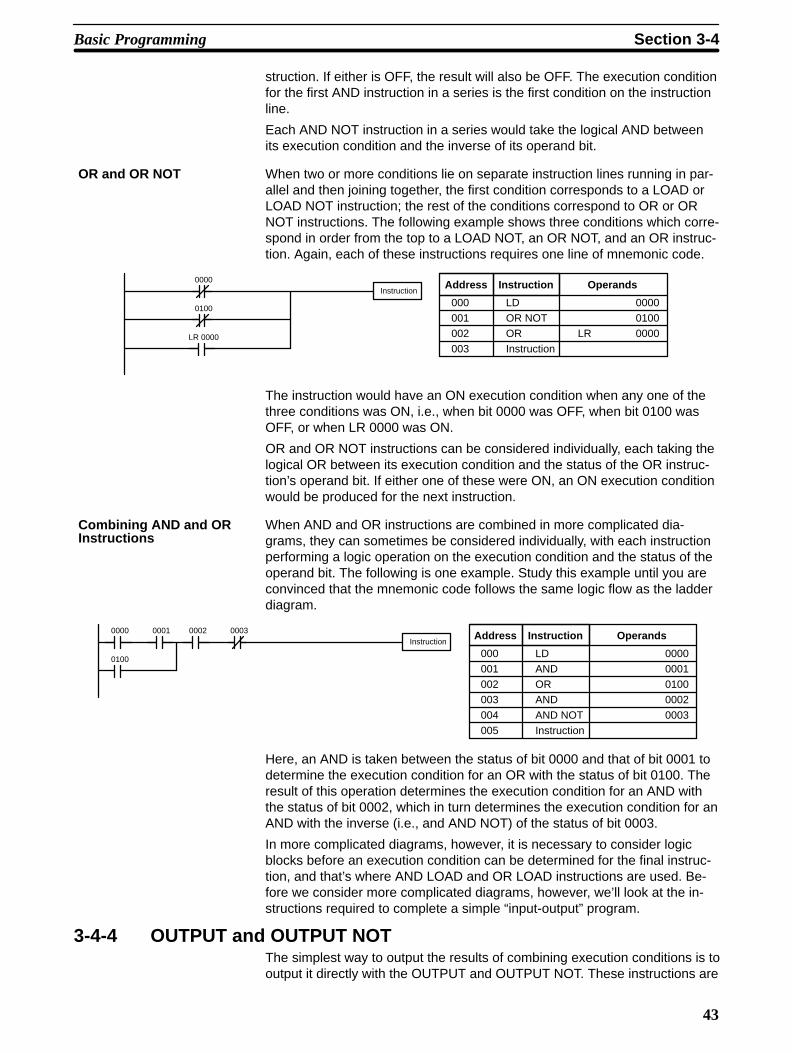
43
struction. If either is OFF, the result will also be OFF. The execution conditionfor the first AND instruction in a series is the first condition on the instructionline.
Each AND NOT instruction in a series would take the logical AND betweenits execution condition and the inverse of its operand bit.
When two or more conditions lie on separate instruction lines running in par-allel and then joining together, the first condition corresponds to a LOAD orLOAD NOT instruction; the rest of the conditions correspond to OR or ORNOT instructions. The following example shows three conditions which corre-spond in order from the top to a LOAD NOT, an OR NOT, and an OR instruc-tion. Again, each of these instructions requires one line of mnemonic code.
Instruction
0100
LR 0000
0000 Address Instruction Operands
000 LD 0000
001 OR NOT 0100
002 OR LR 0000
003 Instruction
The instruction would have an ON execution condition when any one of thethree conditions was ON, i.e., when bit 0000 was OFF, when bit 0100 wasOFF, or when LR 0000 was ON.
OR and OR NOT instructions can be considered individually, each taking thelogical OR between its execution condition and the status of the OR instruc-tion’s operand bit. If either one of these were ON, an ON execution conditionwould be produced for the next instruction.
When AND and OR instructions are combined in more complicated dia-grams, they can sometimes be considered individually, with each instructionperforming a logic operation on the execution condition and the status of theoperand bit. The following is one example. Study this example until you areconvinced that the mnemonic code follows the same logic flow as the ladderdiagram.
Instruction0002 00030000 0001
0100
Address Instruction Operands
000 LD 0000
001 AND 0001
002 OR 0100
003 AND 0002
004 AND NOT 0003
005 Instruction
Here, an AND is taken between the status of bit 0000 and that of bit 0001 todetermine the execution condition for an OR with the status of bit 0100. Theresult of this operation determines the execution condition for an AND withthe status of bit 0002, which in turn determines the execution condition for anAND with the inverse (i.e., and AND NOT) of the status of bit 0003.
In more complicated diagrams, however, it is necessary to consider logicblocks before an execution condition can be determined for the final instruc-tion, and that’s where AND LOAD and OR LOAD instructions are used. Be-fore we consider more complicated diagrams, however, we’ll look at the in-structions required to complete a simple “input-output” program.
3-4-4 OUTPUT and OUTPUT NOTThe simplest way to output the results of combining execution conditions is tooutput it directly with the OUTPUT and OUTPUT NOT. These instructions are
OR and OR NOT
Combining AND and ORInstructions
Basic Programming Section 3-4

44
used to control the status of the designated operand bit according to the ex-ecution condition. With the OUTPUT instruction, the operand bit will beturned ON as long as the execution condition is ON and will be turned OFFas long as the execution condition is OFF. With the OUTPUT NOT instruc-tion, the operand bit will be turned ON as long as the execution condition isOFF and turned OFF as long as the execution condition is ON. These appearas shown below. In mnemonic code, each of these instructions requires oneline.
0000
0101
0100
0001
Address Instruction Operands
000 LD 0000
001 OUT 0100
Address Instruction Operands
000 LD 0001
001 OUT NOT 0101
In the above examples, bit 0100 will be ON as long as bit 0000 is ON and bit0101 will be OFF as long as bit 0001 is ON. Here, bit 0000 and bit 0001 areinput bits and bit 0100 and bit 0101 are output bits, i.e., the signals coming inthrough inputs 0 and 1 are controlling outputs 0 and 1, respectively.
The length of time that a bit is ON or OFF can be controlled by combining theOUTPUT or OUTPUT NOT instruction with Timer instructions. Refer to Ex-amples under 3-7-14 Timer - TIM for details.
3-4-5 The END InstructionThe last instruction required to complete a simple program is the END in-struction. When the CPU scans the program, it executes all instruction up tothe first END instruction before returning to the beginning of the program andbeginning execution again. Although an END instruction can be placed atany point in a program, which is sometimes done when debugging, no in-structions past the first END instruction will be executed until it is removed.The number following the END instruction in the mnemonic code is its func-tion code, which is used when inputting most instructions into the PC. Theseare described later. The END instruction requires no operands and no condi-tions can be placed on the same instruction line with it.
Instruction0000 0001
END(01)Program executionends here.
Address Instruction Operands
000 LD 0000
001 AND NOT 0001
002 Instruction
003 END(01) ---
If there is no END instruction anywhere in the program, the program will notbe executed at all.
Now you have all of the instructions required to write simple input-output pro-grams. Before we finish with ladder diagram basics and go on to inputting theprogram into the PC, let’s look at logic block instructions (AND LOAD and ORLOAD), which are sometimes necessary even with simple diagrams.
3-4-6 Logic Block Instructions Logic block instructions do not correspond to specific conditions on the lad-der diagram; rather, they describe relationships between logic blocks. TheAND LOAD instruction logically ANDs the execution conditions produced bytwo logic blocks. The OR LOAD instruction logically ORs the execution con-ditions produced by two logic blocks.
Basic Programming Section 3-4
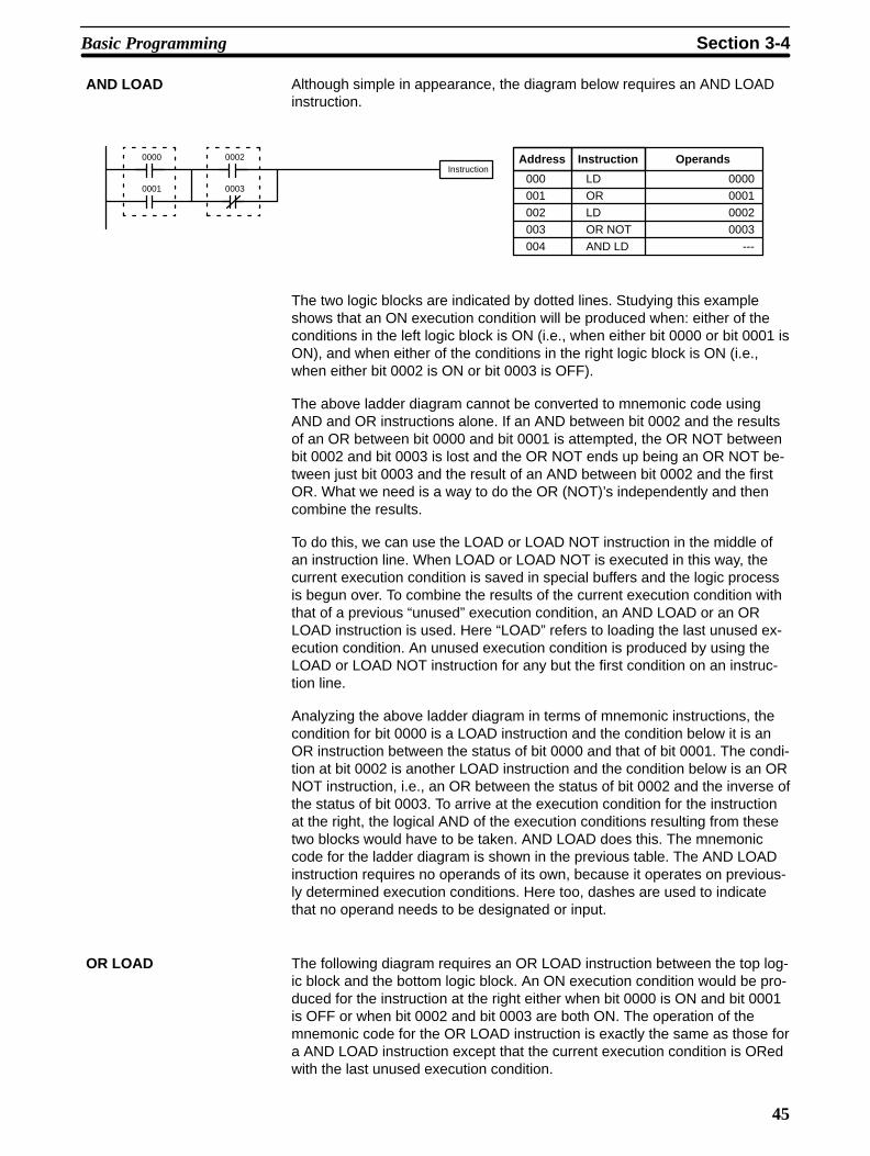
45
Although simple in appearance, the diagram below requires an AND LOADinstruction.
Instruction0002
0003
0000
0001
Address Instruction Operands
000 LD 0000
001 OR 0001
002 LD 0002
003 OR NOT 0003
004 AND LD ---
The two logic blocks are indicated by dotted lines. Studying this exampleshows that an ON execution condition will be produced when: either of theconditions in the left logic block is ON (i.e., when either bit 0000 or bit 0001 isON), and when either of the conditions in the right logic block is ON (i.e.,when either bit 0002 is ON or bit 0003 is OFF).
The above ladder diagram cannot be converted to mnemonic code usingAND and OR instructions alone. If an AND between bit 0002 and the resultsof an OR between bit 0000 and bit 0001 is attempted, the OR NOT betweenbit 0002 and bit 0003 is lost and the OR NOT ends up being an OR NOT be-tween just bit 0003 and the result of an AND between bit 0002 and the firstOR. What we need is a way to do the OR (NOT)’s independently and thencombine the results.
To do this, we can use the LOAD or LOAD NOT instruction in the middle ofan instruction line. When LOAD or LOAD NOT is executed in this way, thecurrent execution condition is saved in special buffers and the logic processis begun over. To combine the results of the current execution condition withthat of a previous “unused” execution condition, an AND LOAD or an ORLOAD instruction is used. Here “LOAD” refers to loading the last unused ex-ecution condition. An unused execution condition is produced by using theLOAD or LOAD NOT instruction for any but the first condition on an instruc-tion line.
Analyzing the above ladder diagram in terms of mnemonic instructions, thecondition for bit 0000 is a LOAD instruction and the condition below it is anOR instruction between the status of bit 0000 and that of bit 0001. The condi-tion at bit 0002 is another LOAD instruction and the condition below is an ORNOT instruction, i.e., an OR between the status of bit 0002 and the inverse ofthe status of bit 0003. To arrive at the execution condition for the instructionat the right, the logical AND of the execution conditions resulting from thesetwo blocks would have to be taken. AND LOAD does this. The mnemoniccode for the ladder diagram is shown in the previous table. The AND LOADinstruction requires no operands of its own, because it operates on previous-ly determined execution conditions. Here too, dashes are used to indicatethat no operand needs to be designated or input.
The following diagram requires an OR LOAD instruction between the top log-ic block and the bottom logic block. An ON execution condition would be pro-duced for the instruction at the right either when bit 0000 is ON and bit 0001is OFF or when bit 0002 and bit 0003 are both ON. The operation of themnemonic code for the OR LOAD instruction is exactly the same as those fora AND LOAD instruction except that the current execution condition is ORedwith the last unused execution condition.
AND LOAD
OR LOAD
Basic Programming Section 3-4

46
Instruction0000 0001
0002 0003
Address Instruction Operands
000 LD 0000
001 AND NOT 0001
002 LD 0002
003 AND 0003
004 OR LD ---
Naturally, some diagrams will require both AND LOAD and OR LOAD instruc-tions.
To code diagrams with logic block instructions in series, the diagram must bedivided into logic blocks. Each block is coded as normal using a LOAD in-struction to code the first condition, and then AND LOAD or OR LOAD isused to logically combine the blocks. First input the first two logic blocks andthen the logic block instruction to combine the results. Then input each addi-tional logic block along with the logic block instruction required to combine itwith the previous result. Examples are given next.
The following diagram requires AND LOAD to be converted to mnemoniccode because three pairs of parallel conditions lie in series.
0000 0002 0004
0001 0003 0005
0100 Address Instruction Operands
000 LD 0000
001 OR NOT 0001
002 LD NOT 0002
003 OR 0003
004 AND LD —
005 LD 0004
006 OR 0005
007 AND LD —
008 OUT 0100
The following diagram requires OR LOAD instructions to be converted tomnemonic code because three pairs of conditions in series lie in parallel toeach other. The first of each pair of conditions is converted to LOAD with theassigned bit operand and then ANDed with the other condition. The first twoblocks are coded first, followed by OR LOAD, the last block, and another ORLOAD.
0000 0001
0002 0003
00040 0005
0101 Address Instruction Operands
000 LD 0000
001 AND NOT 0001
002 LD NOT 0002
003 AND NOT 0003
004 OR LD —
005 LD 0004
006 AND 0005
007 OR LD —
008 OUT 0101
AND LOAD and OR LOAD can naturally be used in the same section of pro-gram. The following diagram contains only two logic blocks as shown. It isnot necessary to further separate block b components, because it can codeddirectly using only AND and OR.
Logic Block Instructions inSeries
Combining AND LOAD andOR LOAD
Basic Programming Section 3-4
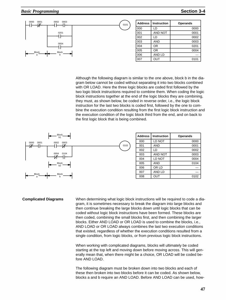
47
0000 0001 0002 0003
0201
0101
0004
Blocka
Blockb
Address Instruction Operands
000 LD 0000
001 AND NOT 0001
002 LD 0002
003 AND 0003
004 OR 0201
005 OR 0004
006 AND LD —
007 OUT 0101
Although the following diagram is similar to the one above, block b in the dia-gram below cannot be coded without separating it into two blocks combinedwith OR LOAD. Here the three logic blocks are coded first followed by thetwo logic block instructions required to combine them. When coding the logicblock instructions together at the end of the logic blocks they are combining,they must, as shown below, be coded in reverse order, i.e., the logic blockinstruction for the last two blocks is coded first, followed by the one to com-bine the execution condition resulting from the first logic block instruction andthe execution condition of the logic block third from the end, and on back tothe first logic block that is being combined.
0000 0001 0002 00030102
0004 0104
Blocka
Blockb
Blockb2
Blockb1 Address Instruction Operands
000 LD NOT 0000
001 AND 0001
002 LD 0002
003 AND NOT 0003
004 LD NOT 0004
005 AND 0104
006 OR LD —
007 AND LD —
008 OUT 0102
When determining what logic block instructions will be required to code a dia-gram, it is sometimes necessary to break the diagram into large blocks andthen continue breaking the large blocks down until logic blocks that can becoded without logic block instructions have been formed. These blocks arethen coded, combining the small blocks first, and then combining the largerblocks. Either AND LOAD or OR LOAD is used to combine the blocks, i.e.,AND LOAD or OR LOAD always combines the last two execution conditionsthat existed, regardless of whether the execution conditions resulted from asingle condition, from logic blocks, or from previous logic block instructions.
When working with complicated diagrams, blocks will ultimately be codedstarting at the top left and moving down before moving across. This will gen-erally mean that, when there might be a choice, OR LOAD will be coded be-fore AND LOAD.
The following diagram must be broken down into two blocks and each ofthese then broken into two blocks before it can be coded. As shown below,blocks a and b require an AND LOAD. Before AND LOAD can be used, how-
Complicated Diagrams
Basic Programming Section 3-4
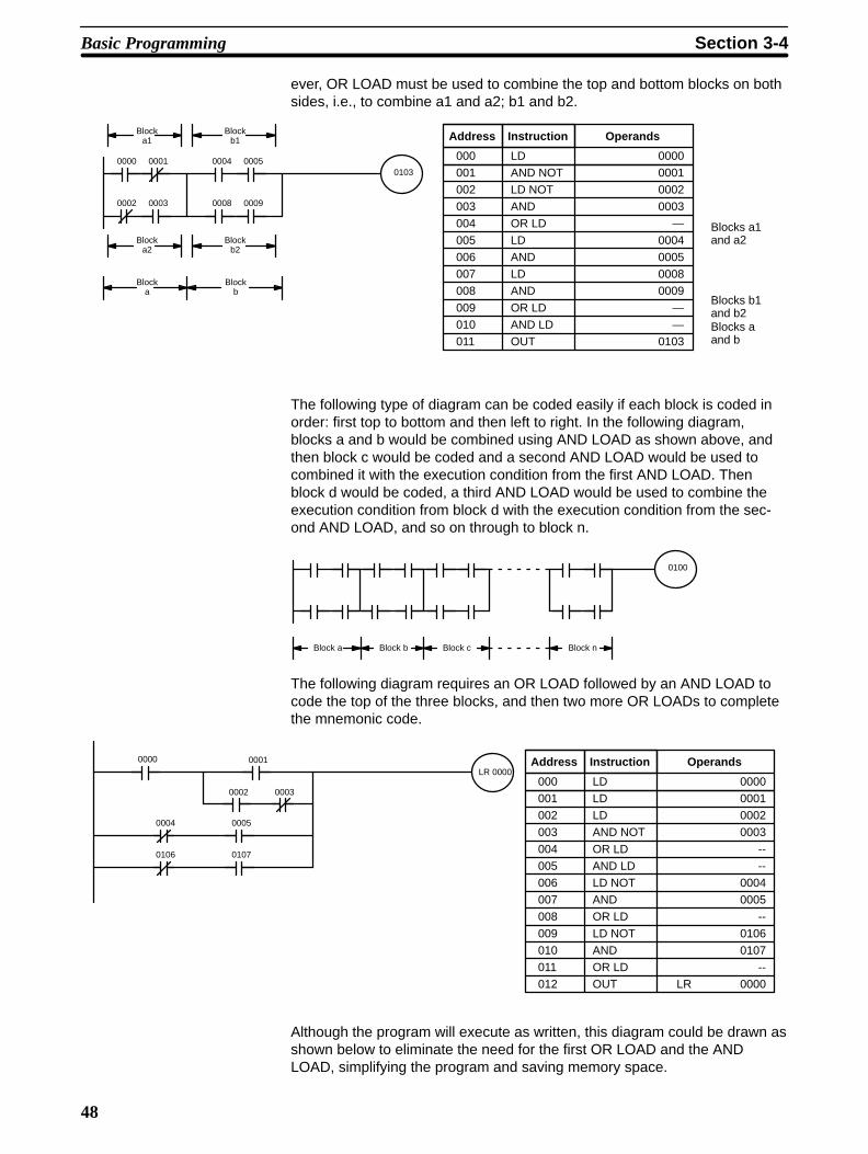
48
ever, OR LOAD must be used to combine the top and bottom blocks on bothsides, i.e., to combine a1 and a2; b1 and b2.
0000 0001 0004 00050103
Blocka
Blockb
0008 0009
Blockb2
Blockb1
0002 0003
Blocka2
Blocka1
Blocks a1and a2
Blocks b1and b2Blocks aand b
Address Instruction Operands
000 LD 0000
001 AND NOT 0001
002 LD NOT 0002
003 AND 0003
004 OR LD —
005 LD 0004
006 AND 0005
007 LD 0008
008 AND 0009
009 OR LD —
010 AND LD —
011 OUT 0103
The following type of diagram can be coded easily if each block is coded inorder: first top to bottom and then left to right. In the following diagram,blocks a and b would be combined using AND LOAD as shown above, andthen block c would be coded and a second AND LOAD would be used tocombined it with the execution condition from the first AND LOAD. Thenblock d would be coded, a third AND LOAD would be used to combine theexecution condition from block d with the execution condition from the sec-ond AND LOAD, and so on through to block n.
Block bBlock a
0100
Block nBlock c
The following diagram requires an OR LOAD followed by an AND LOAD tocode the top of the three blocks, and then two more OR LOADs to completethe mnemonic code.
0002 0003
LR 0000
0000 0001
0004 0005
0106 0107
Address Instruction Operands
000 LD 0000
001 LD 0001
002 LD 0002
003 AND NOT 0003
004 OR LD --
005 AND LD --
006 LD NOT 0004
007 AND 0005
008 OR LD --
009 LD NOT 0106
010 AND 0107
011 OR LD --
012 OUT LR 0000
Although the program will execute as written, this diagram could be drawn asshown below to eliminate the need for the first OR LOAD and the ANDLOAD, simplifying the program and saving memory space.
Basic Programming Section 3-4
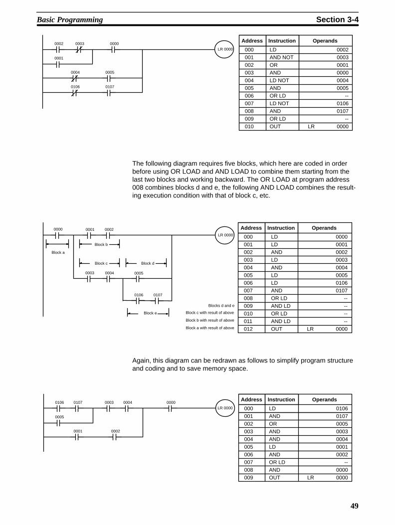
49
0002 0003LR 0000
0001
0000
0004 0005
0106 0107
Address Instruction Operands
000 LD 0002
001 AND NOT 0003
002 OR 0001
003 AND 0000
004 LD NOT 0004
005 AND 0005
006 OR LD --
007 LD NOT 0106
008 AND 0107
009 OR LD --
010 OUT LR 0000
The following diagram requires five blocks, which here are coded in orderbefore using OR LOAD and AND LOAD to combine them starting from thelast two blocks and working backward. The OR LOAD at program address008 combines blocks d and e, the following AND LOAD combines the result-ing execution condition with that of block c, etc.
LR 0000
0000
0003 0004
0106 0107
0001 0002
0005
Block e
Block dBlock c
Block b
Block a
Address Instruction Operands
Blocks d and e
Block c with result of above
Block b with result of above
Block a with result of above
000 LD 0000
001 LD 0001
002 AND 0002
003 LD 0003
004 AND 0004
005 LD 0005
006 LD 0106
007 AND 0107
008 OR LD --
009 AND LD --
010 OR LD --
011 AND LD --
012 OUT LR 0000
Again, this diagram can be redrawn as follows to simplify program structureand coding and to save memory space.
0106 0107LR 0000
0005
0001 0002
0003 0004 0000Address Instruction Operands
000 LD 0106
001 AND 0107
002 OR 0005
003 AND 0003
004 AND 0004
005 LD 0001
006 AND 0002
007 OR LD --
008 AND 0000
009 OUT LR 0000
Basic Programming Section 3-4
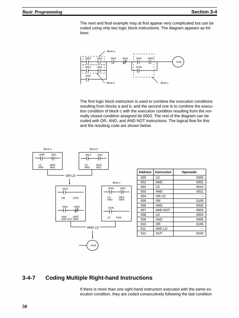
50
The next and final example may at first appear very complicated but can becoded using only two logic block instructions. The diagram appears as fol-lows:
0000 0001
0100
0002 0003
0010 0011
0004 0005
0100
0106
Block cBlock b
Block a
The first logic block instruction is used to combine the execution conditionsresulting from blocks a and b, and the second one is to combine the execu-tion condition of block c with the execution condition resulting from the nor-mally closed condition assigned bit 0003. The rest of the diagram can becoded with OR, AND, and AND NOT instructions. The logical flow for thisand the resulting code are shown below.
0000 0001
0100
0002 0003
0010 0011
0004 00050100
0106
Block c
Block bBlock a
OR LD
LD 0000AND 0001
OR 0100
AND 0002AND NOT 0003
LD 0010AND 0011
LD 0106
LD 0004AND 0005
AND LD
Address Instruction Operands
000 LD 0000
001 AND 0001
002 LD 0010
003 AND 0011
004 OR LD --
005 OR 0100
006 AND 0002
007 AND NOT 0003
008 LD 0004
009 AND 0005
010 OR 0106
011 AND LD --
012 OUT 0100
3-4-7 Coding Multiple Right-hand Instructions
If there is more than one right-hand instruction executed with the same ex-ecution condition, they are coded consecutively following the last condition
Basic Programming Section 3-4

51
on the instruction line. In the following example, the last instruction line con-tains one more condition that corresponds to an AND with bit 0004.
0000 0003
0001
00040002
DR 0000
DR 0001
0100
0106
Address Instruction Operands
000 LD 0000
001 OR 0001
002 OR 0002
003 OR DR 0000
004 AND 0003
005 OUT DR 0001
006 OUT 0100
007 AND 0004
008 OUT 0106
3-5 Inputting the ProgramOnce a program is written in mnemonic code, it can be input directly into thePC from a Programming Console. Mnemonic code is keyed into ProgramMemory addresses from the Programming Console. Checking the programinvolves a syntax check to see that the program has been written accordingto syntax rules. Once syntax errors are corrected, a trial execution can beginand, finally, correction under actual operating conditions can be made.
The operations required to input a program are explained below. Operationsto modify programs that already exist in memory are also provided in thissection, as well as the procedure to obtain the current scan time.
Before starting to input a program, check to see whether there is a programalready loaded. If there is a program already loaded that you do not need,clear it first using the program memory clear key sequence, then input thenew program. If you need the previous program, be sure to check it with theprogram check key sequence and correct it as required.
3-5-1 Initial Programming Console OperationWhen operating the Programming Console for the first time, use the followingprocedure:
1, 2, 3.. 1. Connect the Programming Console to the PC or to the Link Adapter.Make sure that the Programming Console is securely connected; im-proper connection may inhibit operation.
2. Set the mode selector of the Programming Console to PRGM (PRO-GRAM) mode.
3. Turn on the PC.4. The backlight on the display of the Programming Console will light, and
“<PROGRAM> PASSWORD!” will be displayed.5. Press CLR and then MON (the password). “<PROGRAM> BZ” will be
displayed.6. If more then one PC is connected via a Link Adapter, designate the PC.7. Clear memory.
Each of these operations from entering the password on is described in detailin the following subsections. All operations should be done in PROGRAMmode unless otherwise noted.
Password To gain access to the PC’s programming functions, you must first enter thepassword. The password prevents unauthorized access to the program.
The PC prompts you for a password when PC power is turned on or, if PCpower is already on, after the Programming Console has been connected to
Inputting the Program Section 3-5
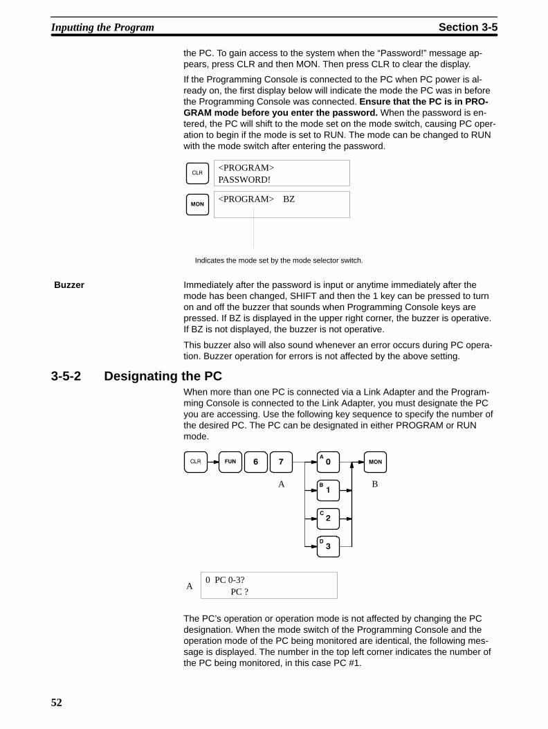
52
the PC. To gain access to the system when the “Password!” message ap-pears, press CLR and then MON. Then press CLR to clear the display.
If the Programming Console is connected to the PC when PC power is al-ready on, the first display below will indicate the mode the PC was in beforethe Programming Console was connected. Ensure that the PC is in PRO-GRAM mode before you enter the password. When the password is en-tered, the PC will shift to the mode set on the mode switch, causing PC oper-ation to begin if the mode is set to RUN. The mode can be changed to RUNwith the mode switch after entering the password.
Indicates the mode set by the mode selector switch.
<PROGRAM>PASSWORD!
<PROGRAM> BZ
Immediately after the password is input or anytime immediately after themode has been changed, SHIFT and then the 1 key can be pressed to turnon and off the buzzer that sounds when Programming Console keys arepressed. If BZ is displayed in the upper right corner, the buzzer is operative.If BZ is not displayed, the buzzer is not operative.
This buzzer also will also sound whenever an error occurs during PC opera-tion. Buzzer operation for errors is not affected by the above setting.
3-5-2 Designating the PCWhen more than one PC is connected via a Link Adapter and the Program-ming Console is connected to the Link Adapter, you must designate the PCyou are accessing. Use the following key sequence to specify the number ofthe desired PC. The PC can be designated in either PROGRAM or RUNmode.
A B
0 PC 0-3? PC ?
A
The PC’s operation or operation mode is not affected by changing the PCdesignation. When the mode switch of the Programming Console and theoperation mode of the PC being monitored are identical, the following mes-sage is displayed. The number in the top left corner indicates the number ofthe PC being monitored, in this case PC #1.
Buzzer
Inputting the Program Section 3-5
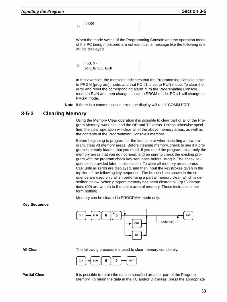
53
1-000B
When the mode switch of the Programming Console and the operation modeof the PC being monitored are not identical, a message like the following onewill be displayed.
<RUN>MODE SET ERR
B
In this example, the message indicates that the Programming Console is setto PRGM (program) mode, and that PC #1 is set to RUN mode. To clear theerror and reset the corresponding alarm, turn the Programming Consolemode to RUN and then change it back to PRGM mode. PC #1 will change toPRGM mode.
Note If there is a communication error, the display will read “COMM ERR”.
3-5-3 Clearing MemoryUsing the Memory Clear operation it is possible to clear part or all of the Pro-gram Memory, work bits, and the DR and TC areas. Unless otherwise speci-fied, the clear operation will clear all of the above memory areas, as well asthe contents of the Programming Console’s memory.
Before beginning to program for the first time or when installing a new pro-gram, clear all memory areas. Before clearing memory, check to see if a pro-gram is already loaded that you need. If you need the program, clear only thememory areas that you do not need, and be sure to check the existing pro-gram with the program check key sequence before using it. The check se-quence is provided later in this section. To clear all memory areas, pressCLR until all zeros are displayed, and then input the keystrokes given in thetop line of the following key sequence. The branch lines shown in the se-quence are used only when performing a partial memory clear, which is de-scribed below. When program memory has been cleared NOP(00) instruc-tions (00) are written to the entire area of memory. These instructions per-form nothing.
Memory can be cleared in PROGRAM mode only.
Key Sequence
[Address]
The following procedure is used to clear memory completely.
It is possible to retain the data in specified areas or part of the ProgramMemory. To retain the data in the TC and/or DR areas, press the appropriate
All Clear
Partial Clear
Inputting the Program Section 3-5
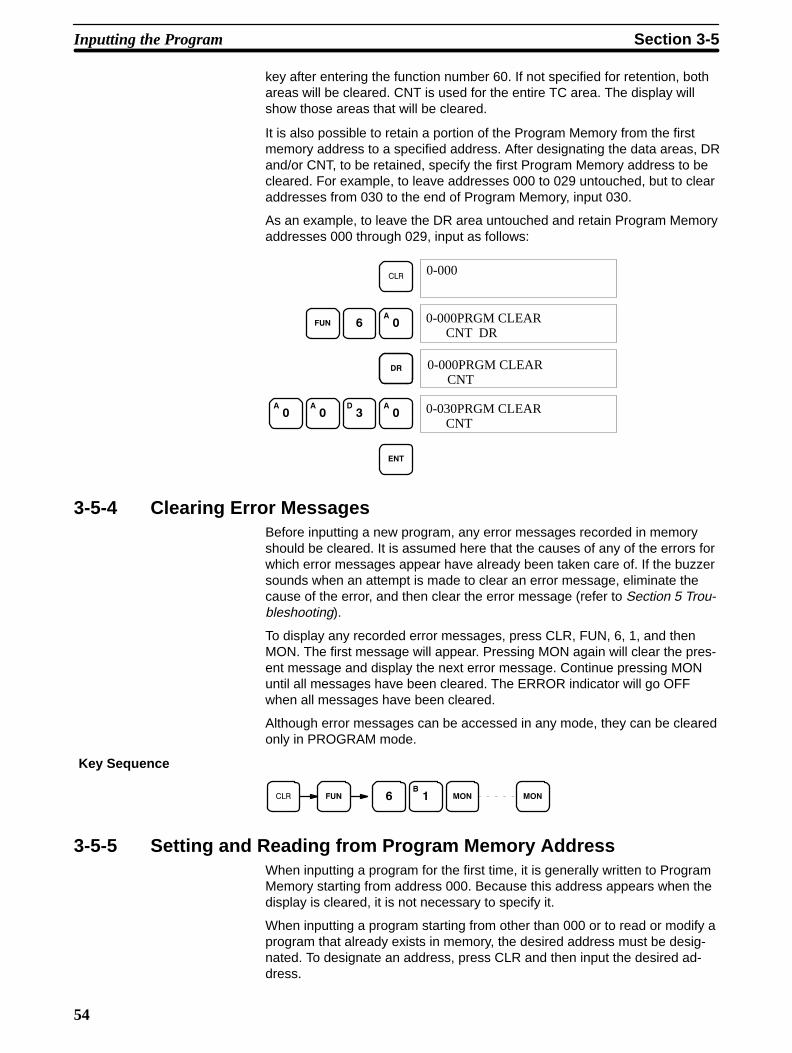
54
key after entering the function number 60. If not specified for retention, bothareas will be cleared. CNT is used for the entire TC area. The display willshow those areas that will be cleared.
It is also possible to retain a portion of the Program Memory from the firstmemory address to a specified address. After designating the data areas, DRand/or CNT, to be retained, specify the first Program Memory address to becleared. For example, to leave addresses 000 to 029 untouched, but to clearaddresses from 030 to the end of Program Memory, input 030.
As an example, to leave the DR area untouched and retain Program Memoryaddresses 000 through 029, input as follows:
0-000
0-000PRGM CLEAR CNT DR
0-000PRGM CLEAR CNT
0-030PRGM CLEAR CNT
3-5-4 Clearing Error MessagesBefore inputting a new program, any error messages recorded in memoryshould be cleared. It is assumed here that the causes of any of the errors forwhich error messages appear have already been taken care of. If the buzzersounds when an attempt is made to clear an error message, eliminate thecause of the error, and then clear the error message (refer to Section 5 Trou-bleshooting).
To display any recorded error messages, press CLR, FUN, 6, 1, and thenMON. The first message will appear. Pressing MON again will clear the pres-ent message and display the next error message. Continue pressing MONuntil all messages have been cleared. The ERROR indicator will go OFFwhen all messages have been cleared.
Although error messages can be accessed in any mode, they can be clearedonly in PROGRAM mode.
Key Sequence
3-5-5 Setting and Reading from Program Memory AddressWhen inputting a program for the first time, it is generally written to ProgramMemory starting from address 000. Because this address appears when thedisplay is cleared, it is not necessary to specify it.
When inputting a program starting from other than 000 or to read or modify aprogram that already exists in memory, the desired address must be desig-nated. To designate an address, press CLR and then input the desired ad-dress.
Inputting the Program Section 3-5
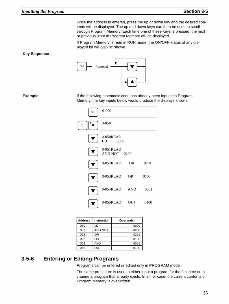
55
Once the address is entered, press the up or down key and the desired con-tents will be displayed. The up and down keys can then be used to scrollthrough Program Memory. Each time one of these keys is pressed, the nextor previous word in Program Memory will be displayed.
If Program Memory is read in RUN mode, the ON/OFF status of any dis-played bit will also be shown.
Key Sequence
If the following mnemonic code has already been input into ProgramMemory, the key inputs below would produce the displays shown.
0-000
0-050
0-050READ LD 0000
0-051READ AND NOT 0200
0-052READ OR 0201
0-053READ OR 0100
0-054READ AND 0001
0-055READ OUT 0100
050 LD 0000
051 AND NOT 0200
052 OR 0201
053 OR 0100
054 AND 0001
055 OUT 0100
Address Instruction Operands
3-5-6 Entering or Editing ProgramsPrograms can be entered or edited only in PROGRAM mode.
The same procedure is used to either input a program for the first time or tochange a program that already exists. In either case, the current contents ofProgram Memory is overwritten.
Example
Inputting the Program Section 3-5

56
To input a program, just follow the mnemonic code that was produced fromthe ladder diagram, ensuring that the proper address is set before starting.Once the proper address is displayed, input the first instruction word, andinput any operands required, pressing ENT after each operand is typed intothe Programming Console, i.e., ENT is pressed at the end of each line of themnemonic code. When ENT is pressed, the designated instruction will beentered and the next display will appear. If the instruction requires two ormore words, the next display will indicate the next operand required and pro-vide a default value for it. If the instruction requires only one word, the nextaddress will be displayed. Continue inputting each line of the mnemonic codeuntil the entire program has been entered.
When inputting numeric values for operands, it is not necessary to input lead-ing zeros. Leading zeros are required only when inputting function codes(see below). When designating operands, be sure to designate the data areafor all DR and LR addresses by pressing the corresponding data area key,and to designate each constant by pressing CONT/#. CONT/# is not requiredfor counter or timer SVs (see below).TC numbers as bit operands (i.e., com-pletion flags) are designated by pressing either TIM or CNT before the ad-dress, depending on whether the TC number has been used to define a timeror a counter. To designate an indirect DR address, press CH/* before DR.
The SV (set value) for a timer or counter is generally entered as a constant,although inputting the address of a word that holds the SV is also possible.When inputting an SV as a constant, CONT/# is not required; just input thenumeric value and press ENT. To designate a word, press CLR and then in-put the word address as described above.
The most basic instructions are input using the Programming Console keysprovided for them. All other instructions are entered using function codes.These function codes are always written after the instruction’s mnemonic. Ifno function code is given, there should be a Programming Console key forthat instruction.
To input an instruction using a function code, set the address, press FUN,input the function code, input any bit operands or definers required on theinstruction line, and then press ENT.
Note Enter function codes with care.
Key Sequence
[Instruction word]? ?
The following program can be entered using the key inputs shown below.Displays will appear as indicated.
Address Instruction Operands
000 LD 0000
001 TIM 00
# 0150
002 TIMH(21) 01
# 9500
Inputting SV for Countersand Timers
Designating Instructions
Example
Inputting the Program Section 3-5
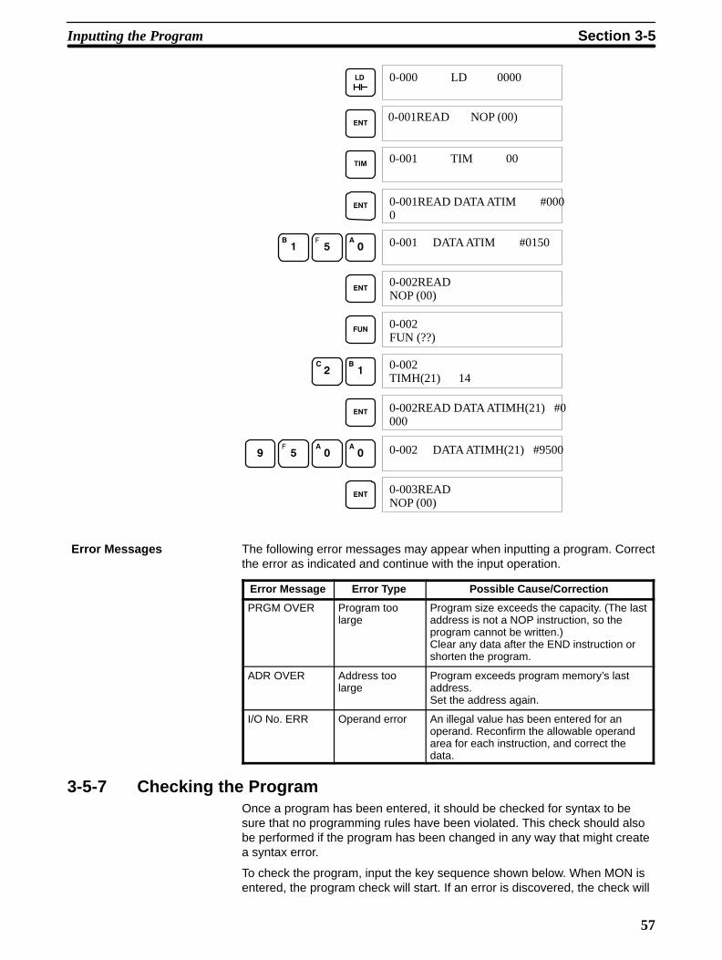
57
0-000 LD 0000
0-001READ NOP (00)
0-001 TIM 00
0-001READ DATA ATIM #0000
0-001 DATA ATIM #0150
0-002READNOP (00)
0-002FUN (??)
0-002TIMH(21) 14
0-002READ DATA ATIMH(21) #0000
0-002 DATA ATIMH(21) #9500
0-003READNOP (00)
The following error messages may appear when inputting a program. Correctthe error as indicated and continue with the input operation.
Error Message Error Type Possible Cause/Correction
PRGM OVER Program toolarge
Program size exceeds the capacity. (The lastaddress is not a NOP instruction, so theprogram cannot be written.)Clear any data after the END instruction orshorten the program.
ADR OVER Address toolarge
Program exceeds program memory’s lastaddress.Set the address again.
I/O No. ERR Operand error An illegal value has been entered for anoperand. Reconfirm the allowable operandarea for each instruction, and correct thedata.
3-5-7 Checking the ProgramOnce a program has been entered, it should be checked for syntax to besure that no programming rules have been violated. This check should alsobe performed if the program has been changed in any way that might createa syntax error.
To check the program, input the key sequence shown below. When MON isentered, the program check will start. If an error is discovered, the check will
Error Messages
Inputting the Program Section 3-5
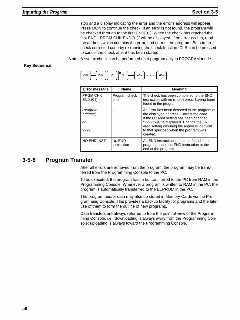
58
stop and a display indicating the error and the error’s address will appear.Press MON to continue the check. If an error is not found, the program willbe checked through to the first END(01). When the check has reached thefirst END, “PRGM CHK END(01)” will be displayed. If an error occurs, readthe address which contains the error, and correct the program. Be sure tocheck corrected code by re-running the check function. CLR can be pressedto cancel the check after it has been started.
Note A syntax check can be performed on a program only in PROGRAM mode.
Key Sequence
Error message Name Meaning
PRGM CHKEND (01)
Program checkend
The check has been completed to the ENDinstruction with no (more) errors having beenfound in the program.
(programaddress) or
????
- An error has been detected in the program atthe displayed address. Correct the code.If the LR area setting has been changed,“????” will be displayed. Change the LRarea setting ensuring the region is identicalto that specified when the program wascreated.
NO END INST No ENDinstruction
An END instruction cannot be found in theprogram. Input the END instruction at theend of the program.
3-5-8 Program Transfer After all errors are removed from the program, the program may be trans-ferred from the Programming Console to the PC.
To be executed, the program has to be transferred to the PC from RAM in theProgramming Console. Whenever a program is written to RAM in the PC, theprogram is automatically transferred to the EEPROM in the PC.
The program and/or data may also be stored in Memory Cards via the Pro-gramming Console. This provides a backup facility for programs and the lateruse of them to form the outline of new programs.
Data transfers are always referred to from the point of view of the Program-ming Console, i.e., downloading is always away from the Programming Con-sole; uploading is always toward the Programming Console.
Inputting the Program Section 3-5
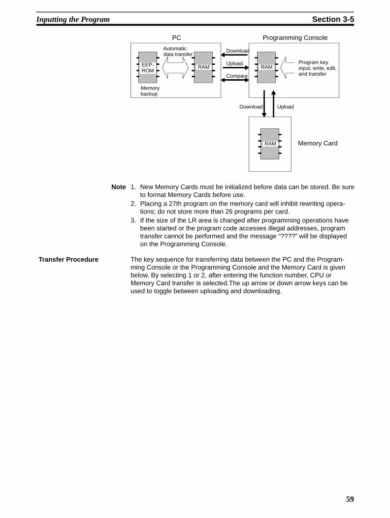
59
PC Programming Console
Memory Card
Automatic data transfer
Memory backup
EEP-ROM
RAM RAM
RAM
Download
Upload
Compare
Download Upload
Program key input, write, edit,and transfer
Note 1. New Memory Cards must be initialized before data can be stored. Be sureto format Memory Cards before use.
2. Placing a 27th program on the memory card will inhibit rewriting opera-tions; do not store more than 26 programs per card.
3. If the size of the LR area is changed after programming operations havebeen started or the program code accesses illegal addresses, programtransfer cannot be performed and the message “????” will be displayedon the Programming Console.
The key sequence for transferring data between the PC and the Program-ming Console or the Programming Console and the Memory Card is givenbelow. By selecting 1 or 2, after entering the function number, CPU orMemory Card transfer is selected.The up arrow or down arrow keys can beused to toggle between uploading and downloading.
Transfer Procedure
Inputting the Program Section 3-5

!
60
Key Sequence
File name
Program trans-ferred to Program-ming Console.
Filedeleted.
DownloadProCo APC
DownloadProCo ACARD
UploadPCAProCo
UploadCARDAProCo
UM
UM+DR
UM
UM+DR
PC
MemoryCard
UM: indicates the users pro-gram, filter value, and LR size.
DR: indicates Data relaymemory’s current contents.
A B
C B
B
Programtransferredto card.
Program trans-ferred to PC or toProgramming Con-sole.
D E
DR area data is usually written tothe PC directly. Hence, if both theprogram and the data in the PC isto be transferred, specify UM+DR.
The Programming Consoles displays at different stages of the keying se-quence are shown below.
0 PRGM TRANSFER? 1.PC 2.CARD
0 PRGM TRANSFER ProCo~PC
0 PRGM TRANSFER? NAME =
0 PRGM TRANSFEREND ProCo~PC
A
B
When 1 or 2 is selected as the response to thisprompt, the display will indicate the selection by plac-ing a flashing cursor over the corresponding number.
The display will indicate the direction of the transfer byuse of an arrow. During transfer, a cursor will flash overthe arrow.
This display indicates the transfer is complete, in thisexample from the Programming Console to the PC.
When writing to a Memory Card, a file name must beassigned to the program to allow identification. The filename can consist of up to a maximum of 8 characters,the allowable characters 0 through 9 and A through F.
B
C
0 PRGM DELETE?U-- 1000
Indicates that a file containing only the user programcalled “1000” will be deleted.D
0 PRGM DELETEEND 1000
Indicates that the file called “1000” has been deleted.
E
Caution Files that have been deleted cannot be recovered. Be sure that you have desig-nated the correct file before pressing the ENT Key.
Inputting the Program Section 3-5

!
61
3-5-9 Program SearchesThe program can be searched for occurrences of any data area address ortimer/counter used in an instruction. Searches can be performed from anycurrently displayed address or from a cleared display.
Once an occurrence of an instruction or bit address has been found, any ad-ditional occurrences of the same instruction or bit can be found by pressingMON again.
When the first word of a multiword instruction is displayed for a search opera-tion, the other words of the instruction can be displayed by pressing the downkey before continuing the search.
Key Sequence
[Bit Address]
0-000
0-000CONT SEARCH 0000
0-000CONT SEARCH 0200
0-051CONT SEARCHAND NOT 0200
3-5-10 Inserting and Deleting InstructionsIn PROGRAM mode, any instruction that is currently displayed can be de-leted or another instruction can be inserted before it. These operations arenot possible in RUN mode.
To insert an instruction, display the instruction before which you want the newinstruction to be placed, input the instruction word in the same way as wheninputting a program initially, and then press INS and the down key. If otherwords are required for the instruction, input these in the same way as wheninputting the program initially.
To delete an instruction, display the instruction word of the instruction to bedeleted and then press DEL and the up key. All the words for the designatedinstruction will be deleted.
Caution Be careful not to inadvertently delete instructions; there is no way to recoverthem without reinputting them completely.
Example:
Inputting the Program Section 3-5
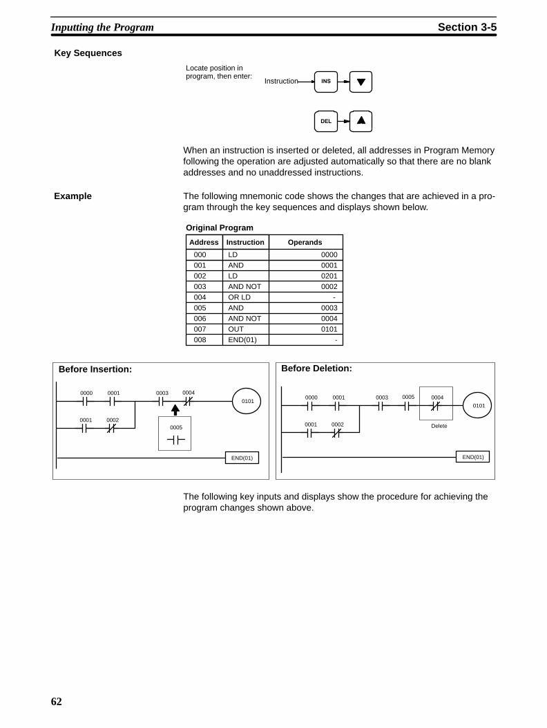
62
Key Sequences
Locate position inprogram, then enter:
Instruction
When an instruction is inserted or deleted, all addresses in Program Memoryfollowing the operation are adjusted automatically so that there are no blankaddresses and no unaddressed instructions.
The following mnemonic code shows the changes that are achieved in a pro-gram through the key sequences and displays shown below.
Original Program
Address Instruction Operands
000 LD 0000
001 AND 0001
002 LD 0201
003 AND NOT 0002
004 OR LD -
005 AND 0003
006 AND NOT 0004
007 OUT 0101
008 END(01) -
00050000 0003 00040001
0001
END(01)
0002
0101
Delete
00040000 0003
0005
0001
0001
END(01)
0002
0101
Before Insertion: Before Deletion:
The following key inputs and displays show the procedure for achieving theprogram changes shown above.
Example
Inputting the Program Section 3-5
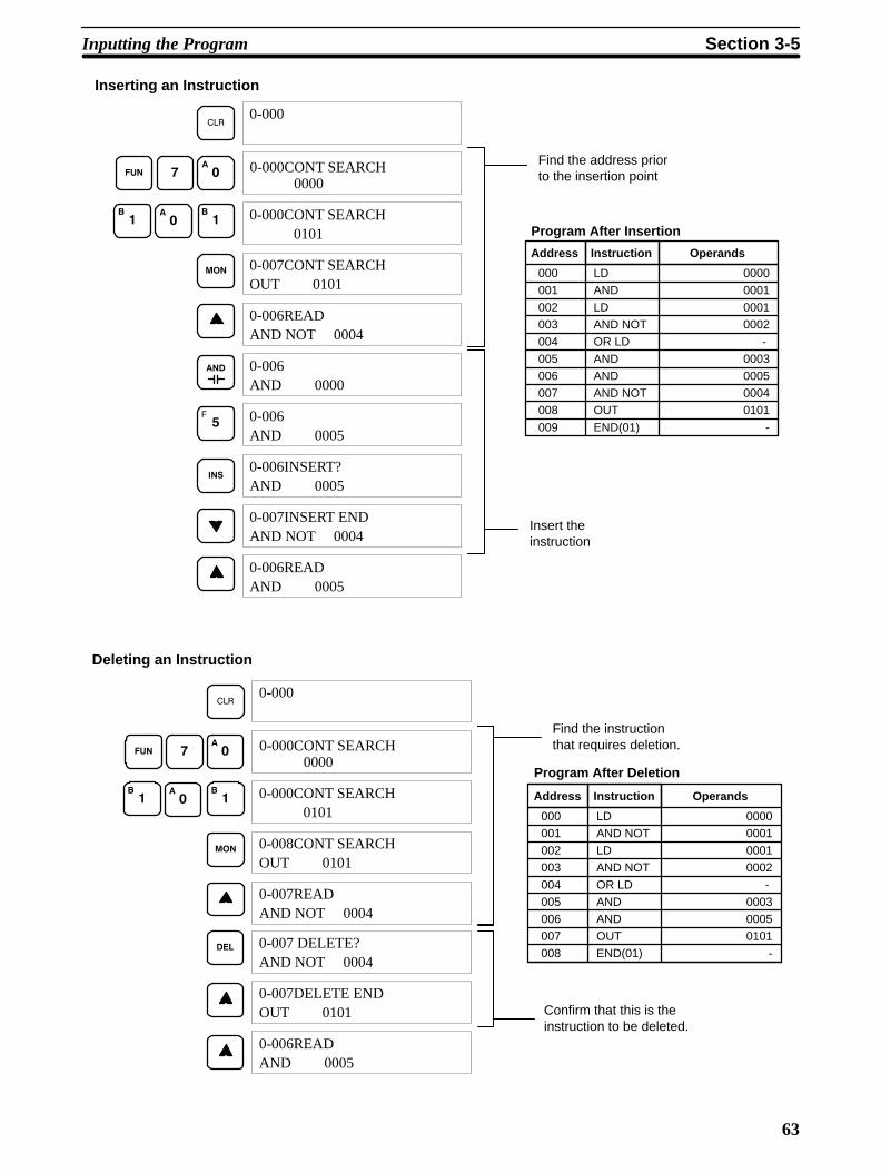
63
0-000CONT SEARCH 0000
Find the address priorto the insertion point
Insert theinstruction
Program After Insertion
Inserting an Instruction
0-000
0-000CONT SEARCH 0101
0-007CONT SEARCHOUT 0101
0-006READAND NOT 0004
0-006AND 0000
0-006AND 0005
0-006INSERT?AND 0005
0-007INSERT ENDAND NOT 0004
0-006READAND 0005
Address Instruction Operands
000 LD 0000
001 AND 0001
002 LD 0001
003 AND NOT 0002
004 OR LD -
005 AND 0003
006 AND 0005
007 AND NOT 0004
008 OUT 0101
009 END(01) -
000 LD 0000
001 AND NOT 0001
002 LD 0001
003 AND NOT 0002
004 OR LD -
005 AND 0003
006 AND 0005
007 OUT 0101
008 END(01) -
Find the instructionthat requires deletion.
Confirm that this is the instruction to be deleted.
Program After Deletion
Deleting an Instruction
0-007 DELETE?AND NOT 0004
0-007DELETE ENDOUT 0101
0-006READAND 0005
Address Instruction Operands
0-000CONT SEARCH 0000
0-000
0-000CONT SEARCH 0101
0-008CONT SEARCHOUT 0101
0-007READAND NOT 0004
Inputting the Program Section 3-5
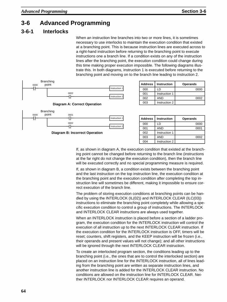
64
3-6 Advanced Programming3-6-1 Interlocks
When an instruction line branches into two or more lines, it is sometimesnecessary to use interlocks to maintain the execution condition that existedat a branching point. This is because instruction lines are executed across toa right-hand instruction before returning to the branching point to executeinstructions one a branch line. If a condition exists on any of the instructionlines after the branching point, the execution condition could change duringthis time making proper execution impossible. The following diagrams illus-trate this. In both diagrams, instruction 1 is executed before returning to thebranching point and moving on to the branch line leading to instruction 2.
Instruction 1
0002
0000
Instruction 2
Branching point
Instruction 1
0002
0000
Instruction 2
Branching point
Diagram B: Incorrect Operation
Diagram A: Correct Operation
0001
Address Instruction Operands
000 LD 0000
001 Instruction 1
002 AND 0002
003 Instruction 2
Address Instruction Operands
000 LD 0000
001 AND 0001
002 Instruction 1
003 AND 0002
004 Instruction 2
If, as shown in diagram A, the execution condition that existed at the branch-ing point cannot be changed before returning to the branch line (instructionsat the far right do not change the execution condition), then the branch linewill be executed correctly and no special programming measure is required.
If, as shown in diagram B, a condition exists between the branching pointand the last instruction on the top instruction line, the execution condition atthe branching point and the execution condition after completing the top in-struction line will sometimes be different, making it impossible to ensure cor-rect execution of the branch line.
The problem of storing execution conditions at branching points can be han-dled by using the INTERLOCK (IL(02)) and INTERLOCK CLEAR (ILC(03))instructions to eliminate the branching point completely while allowing a spe-cific execution condition to control a group of instructions. The INTERLOCKand INTERLOCK CLEAR instructions are always used together.
When an INTERLOCK instruction is placed before a section of a ladder pro-gram, the execution condition for the INTERLOCK instruction will control theexecution of all instruction up to the next INTERLOCK CLEAR instruction. Ifthe execution condition for the INTERLOCK instruction is OFF, timers will bereset; counters, shift registers, and the KEEP instruction will be frozen (i.e.,their operands and present values will not change); and all other instructionswill be ignored through the next INTERLOCK CLEAR instruction.
To create an interlocked program section, the conditions leading up to thebranching point (i.e., the ones that are to control the interlocked section) areplaced on an instruction line for the INTERLOCK instruction, all of lines lead-ing from the branching point are written as separate instruction lines, andanother instruction line is added for the INTERLOCK CLEAR instruction. Noconditions are allowed on the instruction line for INTERLOCK CLEAR. Nei-ther INTERLOCK nor INTERLOCK CLEAR requires an operand.
Advanced Programming Section 3-6
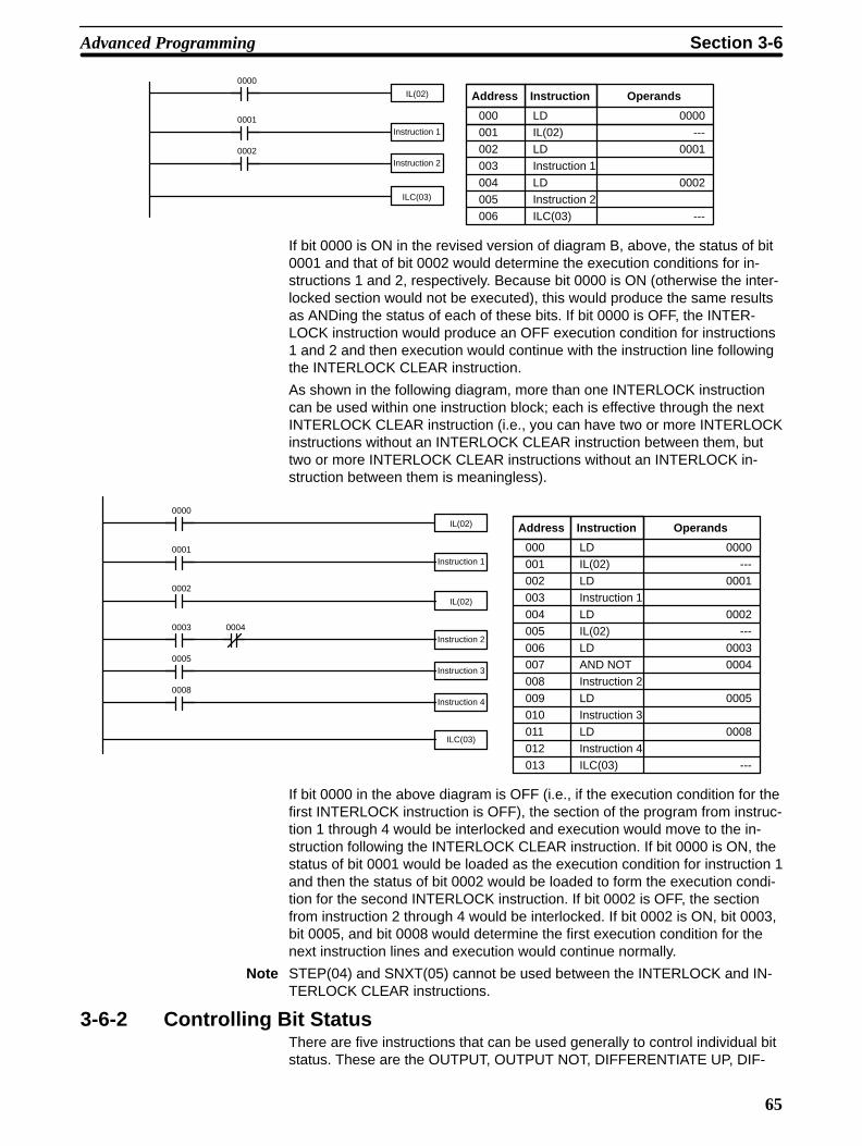
65
Instruction 1
0002
0000
Instruction 2
0001
ILC(03)
IL(02) Address Instruction Operands
000 LD 0000
001 IL(02) ---
002 LD 0001
003 Instruction 1
004 LD 0002
005 Instruction 2
006 ILC(03) ---
If bit 0000 is ON in the revised version of diagram B, above, the status of bit0001 and that of bit 0002 would determine the execution conditions for in-structions 1 and 2, respectively. Because bit 0000 is ON (otherwise the inter-locked section would not be executed), this would produce the same resultsas ANDing the status of each of these bits. If bit 0000 is OFF, the INTER-LOCK instruction would produce an OFF execution condition for instructions1 and 2 and then execution would continue with the instruction line followingthe INTERLOCK CLEAR instruction.
As shown in the following diagram, more than one INTERLOCK instructioncan be used within one instruction block; each is effective through the nextINTERLOCK CLEAR instruction (i.e., you can have two or more INTERLOCKinstructions without an INTERLOCK CLEAR instruction between them, buttwo or more INTERLOCK CLEAR instructions without an INTERLOCK in-struction between them is meaningless).
Instruction 1
0000
Instruction 2
0001
ILC(03)
IL(02)
0004
Instruction 3
Instruction 40008
0005
0003
0002
IL(02)
Address Instruction Operands
000 LD 0000
001 IL(02) ---
002 LD 0001
003 Instruction 1
004 LD 0002
005 IL(02) ---
006 LD 0003
007 AND NOT 0004
008 Instruction 2
009 LD 0005
010 Instruction 3
011 LD 0008
012 Instruction 4
013 ILC(03) ---
If bit 0000 in the above diagram is OFF (i.e., if the execution condition for thefirst INTERLOCK instruction is OFF), the section of the program from instruc-tion 1 through 4 would be interlocked and execution would move to the in-struction following the INTERLOCK CLEAR instruction. If bit 0000 is ON, thestatus of bit 0001 would be loaded as the execution condition for instruction 1and then the status of bit 0002 would be loaded to form the execution condi-tion for the second INTERLOCK instruction. If bit 0002 is OFF, the sectionfrom instruction 2 through 4 would be interlocked. If bit 0002 is ON, bit 0003,bit 0005, and bit 0008 would determine the first execution condition for thenext instruction lines and execution would continue normally.
Note STEP(04) and SNXT(05) cannot be used between the INTERLOCK and IN-TERLOCK CLEAR instructions.
3-6-2 Controlling Bit StatusThere are five instructions that can be used generally to control individual bitstatus. These are the OUTPUT, OUTPUT NOT, DIFFERENTIATE UP, DIF-
Advanced Programming Section 3-6

66
FERENTIATE DOWN, and KEEP instructions. All of these instructions ap-pear as the last instruction in an instruction line and take a bit address for anoperand.These instructions (except for OUTPUT and OUTPUT NOT, whichhave already been introduced) are introduced here because of their impor-tance in most programs. Although these instructions are used to turn ON andOFF output bits (i.e., to send or stop output signals to external devices), theyare also used to control the status of work bits and other bits in memory.
3-6-3 DIFFERENTIATE UP and DIFFERENTIATE DOWN
DIFFERENTIATE UP and DIFFERENTIATE DOWN instructions are used toturn the operand bit ON for one scan at a time. The DIFFERENTIATE UPinstruction turns ON the operand bit for one scan after the execution condi-tion for it goes from OFF to ON; the DIFFERENTIATE DOWN instructionturns ON the operand bit for one scan after the execution condition for it goesfrom ON to OFF. Both of these instructions require only one line of mnemoniccode.
0000
0001
DIFU(10) 0200
DIFD(11) 0201
Address Instruction Operands
000 LD 0000
001 DIFU(10) 0200
Address Instruction Operands
000 LD 0001
001 DIFD(11) 0201
Here, bit 0200 will be turned ON for one scan after bit 0000 goes ON. Thenext time DIFU(10) 0200 is executed, bit 0200 will be turned OFF, regardlessof the status of bit 0000. With the DIFFERENTIATE DOWN instruction, bit0201 will be turned ON for one scan after bit 0001 goes OFF (bit 0201 will bekept OFF until then), and will be turned OFF the next time DIFD(11) 0201 isexecuted.
Up to a total of 16 DIFFERENTIATE UP and DIFFERENTIATE DOWN in-struction can be used in a program.
3-6-4 KEEP
The KEEP instruction is used to maintain the status of the operand bit basedon two execution conditions. To do this, the KEEP instruction is connected totwo instruction lines. When the execution condition at the end of the first in-struction line is ON, the operand bit of the KEEP instruction is turned ON.When the execution condition at the end of the second instruction line is ON,the operand bit of the KEEP instruction is turned OFF. (If both execution con-ditions are ON, the operand bit is also turned OFF.) The operand bit for theKEEP instruction will maintain its ON or OFF status even if it is located in aninterlocked section of the diagram.
In the following example, DR 0000 will be turned ON when bit 0002 is ONand bit 0003 is OFF. DR 0000 will then remain ON until either bit 0004 or bit0005 turns ON. With KEEP, as with all instructions requiring more than one
Advanced Programming Section 3-6
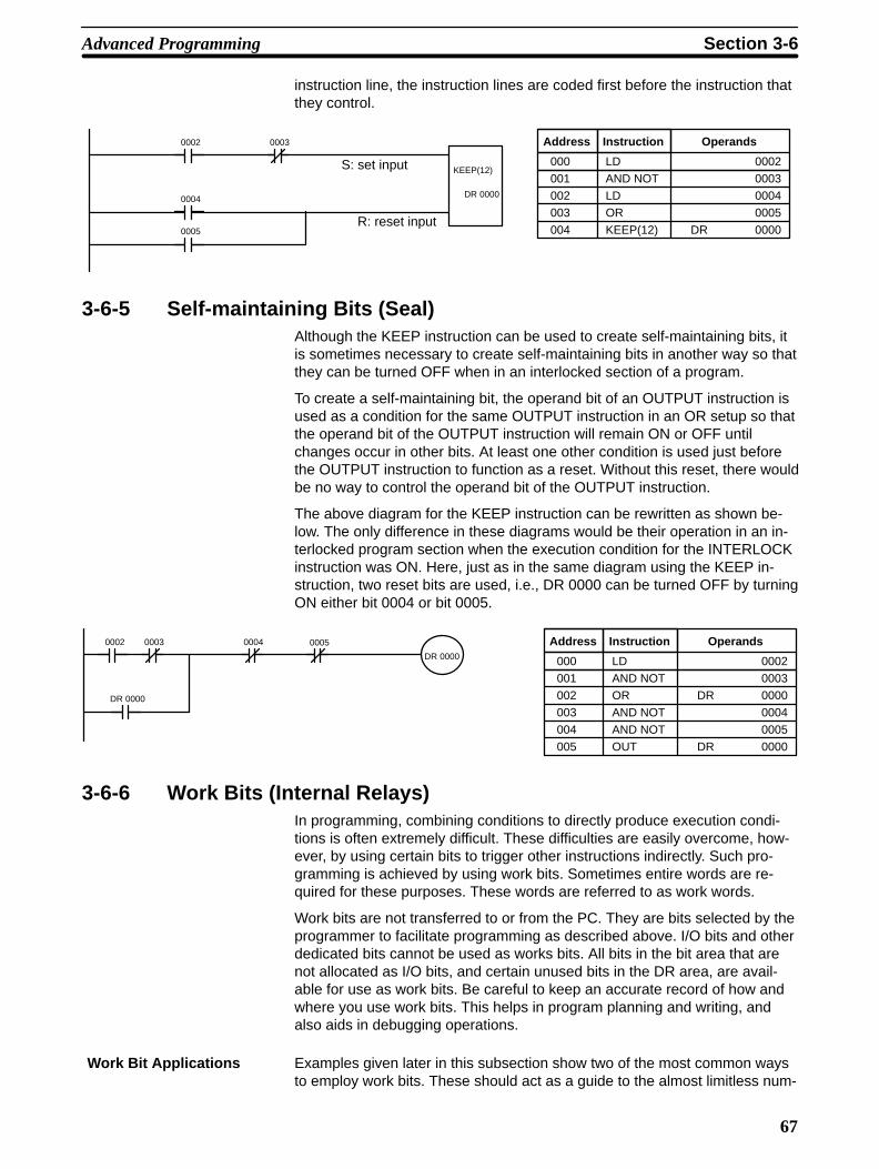
67
instruction line, the instruction lines are coded first before the instruction thatthey control.
KEEP(12)
DR 0000
0002
0004
0003
0005R: reset input
S: set input
Address Instruction Operands
000 LD 0002
001 AND NOT 0003
002 LD 0004
003 OR 0005
004 KEEP(12) DR 0000
3-6-5 Self-maintaining Bits (Seal)Although the KEEP instruction can be used to create self-maintaining bits, itis sometimes necessary to create self-maintaining bits in another way so thatthey can be turned OFF when in an interlocked section of a program.
To create a self-maintaining bit, the operand bit of an OUTPUT instruction isused as a condition for the same OUTPUT instruction in an OR setup so thatthe operand bit of the OUTPUT instruction will remain ON or OFF untilchanges occur in other bits. At least one other condition is used just beforethe OUTPUT instruction to function as a reset. Without this reset, there wouldbe no way to control the operand bit of the OUTPUT instruction.
The above diagram for the KEEP instruction can be rewritten as shown be-low. The only difference in these diagrams would be their operation in an in-terlocked program section when the execution condition for the INTERLOCKinstruction was ON. Here, just as in the same diagram using the KEEP in-struction, two reset bits are used, i.e., DR 0000 can be turned OFF by turningON either bit 0004 or bit 0005.
0002 0003
DR 0000
DR 0000
0004 0005 Address Instruction Operands
000 LD 0002
001 AND NOT 0003
002 OR DR 0000
003 AND NOT 0004
004 AND NOT 0005
005 OUT DR 0000
3-6-6 Work Bits (Internal Relays)In programming, combining conditions to directly produce execution condi-tions is often extremely difficult. These difficulties are easily overcome, how-ever, by using certain bits to trigger other instructions indirectly. Such pro-gramming is achieved by using work bits. Sometimes entire words are re-quired for these purposes. These words are referred to as work words.
Work bits are not transferred to or from the PC. They are bits selected by theprogrammer to facilitate programming as described above. I/O bits and otherdedicated bits cannot be used as works bits. All bits in the bit area that arenot allocated as I/O bits, and certain unused bits in the DR area, are avail-able for use as work bits. Be careful to keep an accurate record of how andwhere you use work bits. This helps in program planning and writing, andalso aids in debugging operations.
Work Bit Applications Examples given later in this subsection show two of the most common waysto employ work bits. These should act as a guide to the almost limitless num-
Advanced Programming Section 3-6

68
ber of ways in which the work bits can be used. Whenever difficulties arise inprogramming a control action, consideration should be given to work bits andhow they might be used to simplify programming.
Work bits are often used with the OUTPUT, OUTPUT NOT, DIFFERENTIATEUP, DIFFERENTIATE DOWN, and KEEP instructions. The work bit is usedfirst as the operand for one of these instructions so that later it can be usedas a condition that will determine how other instructions will be executed.Work bits can also be used with other instructions, e.g., with the SHIFT REG-ISTER instruction (SFT(33)). An example of the use of work words and bitswith the SHIFT REGISTER instruction is provided 3-7-20 SHIFT REGISTER- SFT(33).
Although they are not always specifically referred to as work bits, many of thebits used in the examples later in this section use work bits. Understandingthe use of these bits is essential to effective programming.
Work bits can be used to simplify programming when a certain combinationof conditions is repeatedly used in combination with other conditions. In thefollowing example, bit 0000, bit 0001, bit 0002, and bit 0003 are combined ina logic block that stores the resulting execution condition as the status of bit0103. Bit 0103 is then combined with various other conditions to determineoutput conditions for bit 0000, bit 0001, and bit 0002, i.e., to turn the outputsallocated to these bits ON or OFF.
0000
0003
0001
0004
0002
0005
0004
0009
0008
00050103
0103
0103
0103
0100
0101
0102
Address Instruction Operands
000 LD 0000
001 AND NOT 0001
002 OR 0002
003 OR NOT 0003
004 OUT 0103
005 LD 0103
006 AND 0004
007 AND NOT 0005
008 OUT 0100
009 LD 0103
010 OR NOT 0004
011 AND 0005
012 OUT 0101
013 LD NOT 0103
014 OR 0008
015 OR 0009
016 OUT 0102
Differentiated Conditions Work bits can also be used if differential treatment is necessary for some, butnot all, of the conditions required for execution of an instruction. In this exam-ple, bit 0100 must be left ON continuously as long as bit 0001 is ON and bothbit 0002 and bit 0003 are OFF, or as long as bit 0004 is ON and bit 0005 isOFF. It must be turned ON for only one scan each time bit 0000 turns ON(unless one of the preceding conditions is keeping it ON continuously).
This action is easily programmed by using bit 0200 as a work bit as the oper-and of the DIFFERENTIATE UP instruction (DIFU(10)). When bit 0000 turnsON, bit 0100 will be turned ON for one scan and then be turned OFF the next
Reducing ComplexConditions
Advanced Programming Section 3-6

69
scan by DIFU(10). Assuming the other conditions controlling bit 0100 are notkeeping it ON, the work bit 0200 will turn bit 0100 ON for one scan only.
0200
DIFU(10) 0200
0000
0001 0002 0003
0004 0005
0100
Address Instruction Operands
000 LD 0000
001 DIFU(10) 0200
002 LD 0200
003 LD 0001
004 AND NOT 0002
005 AND NOT 0003
006 OR LD ---
007 LD 0004
008 AND NOT 0005
009 OR LD ---
010 OUT 0100
3-6-7 Programming PrecautionsThe number of conditions that can be used in series or parallel is unlimitedas long as the memory capacity of the PC is not exceeded. Therefore, use asmany conditions as required to draw a clear diagram. Although very compli-cated diagrams can be drawn with instruction lines, there must not be anyconditions on lines running vertically between two other instruction lines. Dia-gram A shown below, for example, is not possible, and should be drawn asdiagram B. Mnemonic code is provided for diagram B only; coding diagram Awould be impossible.
Instruction 2
Instruction 1
0002
0003
0000
0001
0004
Diagram A
Instruction 1
0004
0003
0000
0001
Diagram B
0002
Instruction 2
00040000
0001
Address Instruction Operands
000 LD 0001
001 AND 0004
002 OR 0000
003 AND 0002
004 Instruction 1
005 LD 0000
006 AND 0004
007 OR 0001
008 AND NOT 0003
009 Instruction 2
The number of times any particular bit can be assigned to conditions is notlimited, so use them as many times as required to simplify your program. Of-ten, complicated programs are the result of attempts to reduce the number oftimes a bit is used.
Except for instructions for which conditions are not allowed (e.g., INTER-LOCK CLEAR, see below), every instruction line must also have at least onecondition on it to determine the execution condition for the instruction at theright. Again, diagram A , below, must be drawn as diagram B. If an instructionmust be continuously executed (e.g., if an output must always be kept ONwhile the program is being executed), the Always ON Flag (bit 0408) can beused.
Advanced Programming Section 3-6
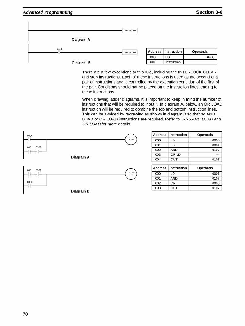
70
Instruction0408
Instruction
Diagram A
Diagram B
Address Instruction Operands
000 LD 0408
001 Instruction
There are a few exceptions to this rule, including the INTERLOCK CLEARand step instructions. Each of these instructions is used as the second of apair of instructions and is controlled by the execution condition of the first ofthe pair. Conditions should not be placed on the instruction lines leading tothese instructions.
When drawing ladder diagrams, it is important to keep in mind the number ofinstructions that will be required to input it. In diagram A, below, an OR LOADinstruction will be required to combine the top and bottom instruction lines.This can be avoided by redrawing as shown in diagram B so that no ANDLOAD or OR LOAD instructions are required. Refer to 3-7-6 AND LOAD andOR LOAD for more details.
0000
0001 0107
0107
0001
0000
01070107
Diagram A
Diagram B
Address Instruction Operands
000 LD 0000
001 LD 0001
002 AND 0107
003 OR LD ---
004 OUT 0107
Address Instruction Operands
000 LD 0001
001 AND 0107
002 OR 0000
003 OUT 0107
Advanced Programming Section 3-6

71
3-7 Instruction SetThe remainder of this section explains SP-series PC instructions individually.
3-7-1 NotationIn the remainder of this manual, all instructions will be referred to by theirmnemonics. For example, the OUTPUT instruction will be called OUT; theAND LOAD instruction, AND LD. If you’re not sure of the instruction a mne-monic is used for, refer to Appendix C Programming Instructions and Execu-tion Times.
If an instruction is assigned a function code, it will be given in parenthesesafter the mnemonic. These function codes, which are 2-digit decimal num-bers, are used to input most instructions into the CPU and are describedbriefly below. A table of instructions listed in order of function codes, is alsoprovided in Appendix C.
3-7-2 Instruction FormatMost instructions have at least one or more operands associated with them.Operands indicate or provide the data on which an instruction is to be per-formed. These are sometimes input as the actual numeric values (i.e., asconstants), but are usually the addresses of data area words or bits that con-tain the data to be used. A bit whose address is designated as an operand iscalled an operand bit; a word whose address is designated as an operand iscalled an operand word. In some instructions, the word address designatedin an instruction indicates the first of multiple words containing the desireddata.
Each instruction requires one or more words in Program Memory. The firstword is the instruction word, which specifies the instruction and contains anydefiners (described below) or operand bits required by the instruction. Otheroperands required by the instruction are contained in following words, oneoperand per word. Some instructions require up to five words.
A definer is an operand associated with an instruction and contained in thesame word as the instruction itself. These operands define the instructionrather than telling what data it is to use. Examples of definers are TC num-bers, which are used in timer and counter instructions to create timers andcounters. Bit operands are also contained in the same word as the instructionitself, although these are not considered definers.
3-7-3 Data Areas, Definer Values, and FlagsIn this section, each instruction description includes its ladder diagram sym-bol, the data areas that can be used by its operands, and the values that canbe used as definers. Details for the data areas are also specified by the oper-and names and the type of data required for each operand (i.e., word or bitand, for words, hexadecimal or BCD).
Not all addresses in the specified data areas are necessarily allowed for anoperand, e.g., if an operand requires two words, the last word in a data areacannot be designated as the first word of the operand because all words for asingle operand must be within the same data area. Other specific limitationsare given in a Limitations subsection. Refer to 3-2 Memory Areas for ad-dressing conventions and the addresses of flags and control bits.
The Flags subsection lists flags that are affected by execution of an instruc-tion. These flags include the following.
Instruction Set Section 3-7

72
Abbreviation Name Bit
ER Instruction Execution Error Flag 0311
CY Carry Flag 0312
LE Less Than Flag 0313
EQ Equals Flag 0314
GR Greater Than Flag 0315
ER is the flag most commonly used for monitoring an instruction’s execution.When ER goes ON, it indicates that an error has occurred in attempting toexecute the current instruction. The Flags subsection of each instruction listspossible reasons for ER being ON. ER will turn ON if operands are not en-tered correctly. Instructions are not executed when ER is ON. A table of in-structions and the flags they affect is provided in Appendix E Error and Arith-metic Flag Operation.
When the DR area is specified for an operand, an indirect address can beused. Indirect DR addressing is specified by placing an asterisk before theDR: *DR.
When an indirect DR address is specified, the designated DR word will con-tain the address of the DR word that contains the data that will be used asthe operand of the instruction. If, for example, *DR 01 was designated as thefirst operand and LR 00 as the second operand of MOV(30), the contents ofDR 01 was 0006, and DR 06 contained 5555, the value 5555 would bemoved to LR 00.
MOV(30)
*DR 01
LR 00
Word ContentDR 00 4C23DR 01 0006DR 02 F3A3
DR 06 5555DR 07 2255DR 08 D1C5
5555moved toLR 00.
Indicates DR 06.
Indirect address
When using indirect addressing, the address of the desired word must be inBCD and it must specify a word within the DR area. In the above example,the content of *DR 00 would have to be in BCD and between 0000 and 1515.
Although data area addresses are most often given as operands, many oper-ands and all definers are input as constants. The available value range for agiven definer or operand depends on the particular instruction that uses it.Constants must also be entered in the form required by the instruction, i.e., inBCD or in hexadecimal.
3-7-4 Coding Right-hand InstructionsWriting mnemonic code for ladder instructions has already been describedfor ladder instructions. Converting the information in the ladder diagram sym-bol for all other instructions follows the same pattern, as described below,and is not specified for each instruction individually.
The first word of any instruction defines the instruction and provides any de-finers. If the instruction requires only a signal bit operand with no definer, the
Indirect Addressing
Designating Constants
Instruction Set Section 3-7
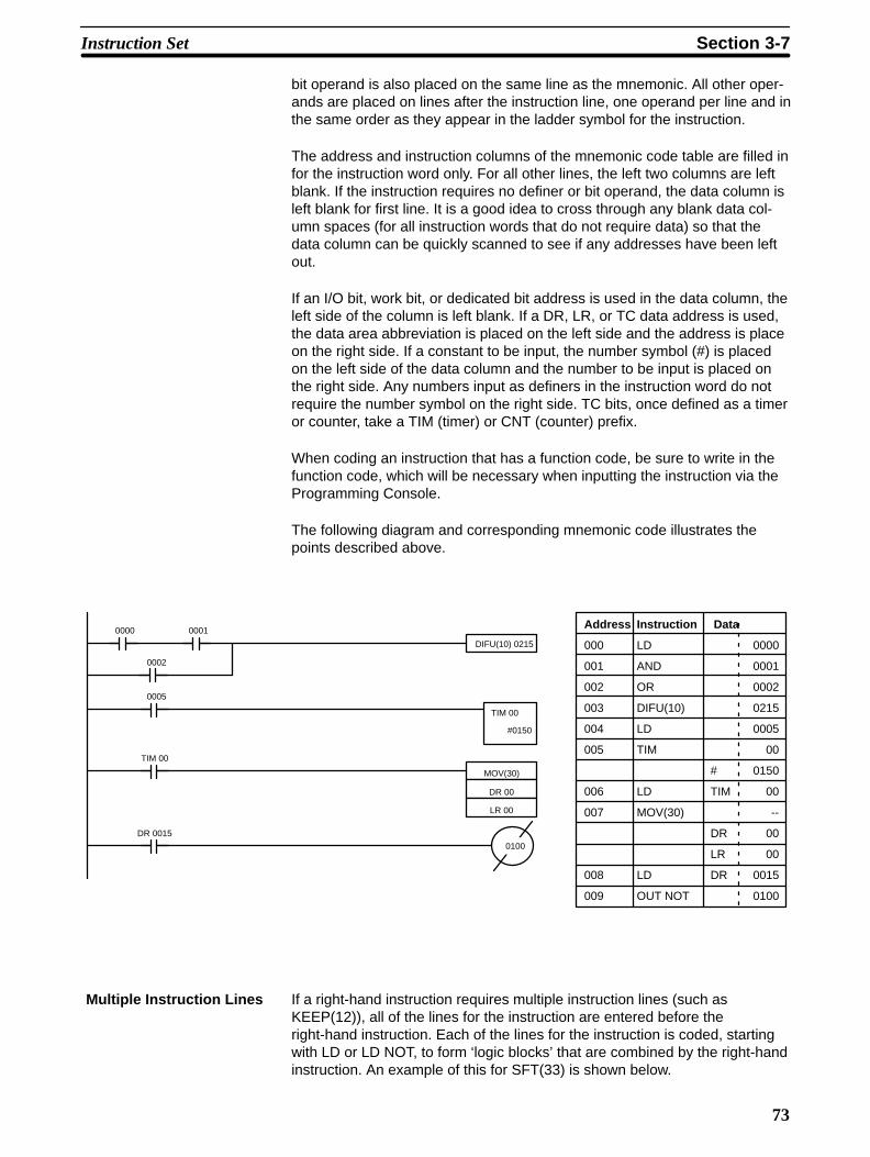
73
bit operand is also placed on the same line as the mnemonic. All other oper-ands are placed on lines after the instruction line, one operand per line and inthe same order as they appear in the ladder symbol for the instruction.
The address and instruction columns of the mnemonic code table are filled infor the instruction word only. For all other lines, the left two columns are leftblank. If the instruction requires no definer or bit operand, the data column isleft blank for first line. It is a good idea to cross through any blank data col-umn spaces (for all instruction words that do not require data) so that thedata column can be quickly scanned to see if any addresses have been leftout.
If an I/O bit, work bit, or dedicated bit address is used in the data column, theleft side of the column is left blank. If a DR, LR, or TC data address is used,the data area abbreviation is placed on the left side and the address is placeon the right side. If a constant to be input, the number symbol (#) is placedon the left side of the data column and the number to be input is placed onthe right side. Any numbers input as definers in the instruction word do notrequire the number symbol on the right side. TC bits, once defined as a timeror counter, take a TIM (timer) or CNT (counter) prefix.
When coding an instruction that has a function code, be sure to write in thefunction code, which will be necessary when inputting the instruction via theProgramming Console.
The following diagram and corresponding mnemonic code illustrates thepoints described above.
Address Instruction Data
000 LD 0000
001 AND 0001
002 OR 0002
003 DIFU(10) 0215
004 LD 0005
005 TIM 00
# 0150
006 LD TIM 00
007 MOV(30) --
DR 00
LR 00
008 LD DR 0015
009 OUT NOT 0100
DIFU(10) 0215
0100
MOV(30)
DR 00
LR 00
TIM 00
0002
0005
DR 0015
0000 0001
TIM 00
#0150
If a right-hand instruction requires multiple instruction lines (such asKEEP(12)), all of the lines for the instruction are entered before theright-hand instruction. Each of the lines for the instruction is coded, startingwith LD or LD NOT, to form ‘logic blocks’ that are combined by the right-handinstruction. An example of this for SFT(33) is shown below.
Multiple Instruction Lines
Instruction Set Section 3-7

74
I
P
R
SFT(33)
DR 00
Address Instruction Data
000 LD 0000
001 AND 0001
002 LD 0002
003 LD 0215
004 AND NOT 0200
005 LD 0201
006 AND NOT 0214
007 AND NOT LR 0000
008 OR LD --
009 AND 0215
010 SFT(33) --
DR 00
011 LD DR 0015
012 OUT NOT 0100
0215 0200
0100
0201 0214 LR 0000
0215
0002
DR 0015
0000 0001
When you have finished coding the program, make sure you have placedEND(01) at the last address. If there is not END(01) instruction in the pro-gram, the program will not be executed even if you switch to RUN mode.
3-7-5 LOAD, LOAD NOT, AND, AND NOT, OR, and OR NOT
B: Bit
I/O, work, dedicated, DR, LR, TC
Ladder Symbols Operand Data Areas
LOAD - LDB
B: Bit
I/O, work, dedicated, DR, LR, TCLOAD NOT - LD NOT B
B: Bit
I/O, work, dedicated, DR, LR, TCAND - AND
B
B: Bit
I/O, work, dedicated, DR, LR, TCAND NOT - AND NOT
B
B: Bit
I/O, work, dedicated, DR, LR, TCOR - OR B
B: Bit
I/O, work, dedicated, DR, LR, TCOR NOT - OR NOT B
There is no limit to the number of any of these instructions, or restrictions inthe order in which they must be used, as long as the memory capacity of thePC is not exceeded.
END(01)
Limitations
Instruction Set Section 3-7
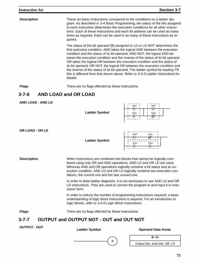
75
These six basic instructions correspond to the conditions on a ladder dia-gram. As described in 3-4 Basic Programming, the status of the bits assignedto each instruction determines the execution conditions for all other instruc-tions. Each of these instructions and each bit address can be used as manytimes as required. Each can be used in as many of these instructions as re-quired.
The status of the bit operand (B) assigned to LD or LD NOT determines thefirst execution condition. AND takes the logical AND between the executioncondition and the status of its bit operand; AND NOT, the logical AND be-tween the execution condition and the inverse of the status of its bit operand.OR takes the logical OR between the execution condition and the status ofits bit operand; OR NOT, the logical OR between the execution condition andthe inverse of the status of its bit operand. The ladder symbol for loading TRbits is different from that shown above. Refer to 3-4-3 Ladder Instructions fordetails.
There are no flags affected by these instructions.
3-7-6 AND LOAD and OR LOAD
Ladder Symbol
AND LOAD - AND LD0002
0003
0000
0001
Ladder Symbol
OR LOAD - OR LD0000 0001
0002 0003
When instructions are combined into blocks that cannot be logically com-bined using only OR and AND operations, AND LD and OR LD are used.Whereas AND and OR operations logically combine a bit status and an ex-ecution condition, AND LD and OR LD logically combine two execution con-ditions, the current one and the last unused one.
In order to draw ladder diagrams, it is not necessary to use AND LD and ORLD instructions. They are used to convert the program to and input it in mne-monic form.
In order to reduce the number of programming instructions required, a basicunderstanding of logic block instructions is required. For an introduction tologic blocks, refer to 3-4-6 Logic Block Instructions.
There are no flags affected by these instructions.
3-7-7 OUTPUT and OUTPUT NOT - OUT and OUT NOT
B: Bit
Output bits, work bits, DR, LR
Ladder Symbol Operand Data AreasOUTPUT - OUT
B
Description
Flags
Description
Flags
Instruction Set Section 3-7
76
B: Bit
Output bits, work bits, DR, LR
Ladder Symbol Operand Data AreasOUTPUT NOT - OUT NOT
B
Any output bit can generally be used in only one instruction that controls itsstatus. Refer to 3-2-2 I/O Bits for details.
OUT and OUT NOT are used to control the status of the designated bit ac-cording to the execution condition.
OUT turns ON the designated bit for an ON execution condition, and turnsOFF the designated bit for an OFF execution condition.
OUT NOT turns ON the designated bit for a OFF execution condition, andturns OFF the designated bit for an ON execution condition.
OUT and OUT NOT can be used to control execution by turning ON and OFFbits that are assigned to conditions on the ladder diagram, thus determiningexecution conditions for other instructions. This is particularly helpful and al-lows a complex set of conditions to be used to control the status of a singlework bit, and then that work bit can be used to control other instructions.
The length of time that a bit is ON or OFF can be controlled by combining theOUT or OUT NOT with TIM. Refer to Examples under 3-7-14 TIMER - TIMfor details.
There are no flags affected by these instructions.
3-7-8 DIFFERENTIATE UP and DIFFERENTIATE DOWN - DIFU(10) and DIFD(11)
B: Bit
Output bits, work bits, DR, LR
Ladder Symbols Operand Data Areas
DIFU(10) B
B: Bit
Output bits, work bits, DR, LRDIFD(11) B
The total of all DIFU(10) and DIFD(11) instruction in any one program mustbe 16 or less. Any output bit can generally be used in only one instructionthat controls its status. Refer to 3-2-2 I/O Bits for details.
DIFU(10) and DIFD(11) are used to turn the designated bit ON for one scanonly.
Whenever executed, DIFU(10) compares its current execution with the pre-vious execution condition. If the previous execution condition was OFF andthe current one is ON, DIFU(10) will turn ON the designated bit. If the pre-vious execution condition was ON and the current execution condition is ei-ther ON or OFF, DIFU(10) will either turn the designated bit OFF or leave itOFF (i.e., if the designated bit is already OFF). The designated bit will thusnever be ON for longer than one scan, assuming it is executed each scan(see Precautions, below).
Limitations
Description
Flags
Limitations
Description
Instruction Set Section 3-7

77
Whenever executed, DIFD(11) compares its current execution with the pre-vious execution condition. If the previous execution condition is ON and thecurrent one is OFF, DIFD(11) will turn ON the designated bit. If the previousexecution condition was OFF and the current execution condition is eitherON or OFF, DIFD(11) will either turn the designated bit OFF or leave it OFF.The designated bit will thus never be ON for longer than one scan, assumingit is executed each scan (see Precautions, below).
There are no flags affected by these instructions.
DIFU(10) and DIFD(11) operation can be uncertain when the instructions areprogrammed between IL and ILC. Refer to 3-7-10 INTERLOCK and INTER-LOCK CLEAR - IL(02) and ILC(03) for details.
In diagram A, below, whenever CMP(32) is executed with an ON executioncondition it will compare the contents of the two operand words (DR 10 andDR 00) and set the arithmetic flags (GR, EQ, and LE) accordingly. If the ex-ecution condition remains ON, flag status may be changed each scan if thecontent of one or both operands change. Diagram B, however, is an exampleof how DIFU(10) can be used to ensure that CMP(32) is executed only onceeach time the desired execution condition goes ON.
0000
CMP(32)
DR 10
DR 00Diagram A
0215
CMP(32)
DR 10
DR 00Diagram B
DIFU(10) 0215
0000
Address Instruction Operands
000 LD 0000
001 CMP(32)
DR 10
DR 00
Address Instruction Operands
000 LD 0000
001 DIFU(10) 0215
002 LD 0215
003 CMP(32)
DR 10
DR 00
The following diagram would be very complicated to draw without usingDIFU(10) because only one of the conditions determining the execution con-dition for MOV(30) requires differentiated treatment.
0215
MOV(30)
DR 10
DR 00
DIFU(10) 0215
0000
0001 0002 0003
0004 0005
Address Instruction Operands
000 LD 0000
001 DIFU(10) 0215
002 LD 0215
003 LD 0001
004 AND NOT 0002
005 AND NOT 0003
006 OR LD ---
007 LD 0004
008 AND NOT 0005
009 OR LD ---
010 MOV(30)
DR 10
DR 00
Flags
Precautions
Example 1: One-timeExecution of OtherInstructions
Example 2: Use to SimplifyProgramming
Instruction Set Section 3-7
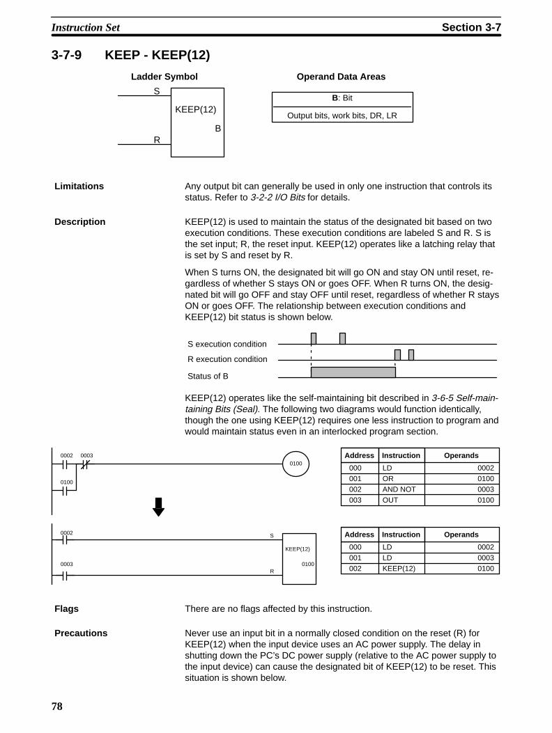
78
3-7-9 KEEP - KEEP(12)
B: Bit
Output bits, work bits, DR, LR
Ladder Symbol Operand Data Areas
S
R
KEEP(12)
B
Any output bit can generally be used in only one instruction that controls itsstatus. Refer to 3-2-2 I/O Bits for details.
KEEP(12) is used to maintain the status of the designated bit based on twoexecution conditions. These execution conditions are labeled S and R. S isthe set input; R, the reset input. KEEP(12) operates like a latching relay thatis set by S and reset by R.
When S turns ON, the designated bit will go ON and stay ON until reset, re-gardless of whether S stays ON or goes OFF. When R turns ON, the desig-nated bit will go OFF and stay OFF until reset, regardless of whether R staysON or goes OFF. The relationship between execution conditions andKEEP(12) bit status is shown below.
S execution condition
R execution condition
Status of B
KEEP(12) operates like the self-maintaining bit described in 3-6-5 Self-main-taining Bits (Seal). The following two diagrams would function identically,though the one using KEEP(12) requires one less instruction to program andwould maintain status even in an interlocked program section.
0002 0003
0100
0100Address Instruction Operands
Address Instruction Operands
000 LD 0002
001 OR 0100
002 AND NOT 0003
003 OUT 0100
000 LD 0002
001 LD 0003
002 KEEP(12) 0100
S
R
KEEP(12)
0100
0002
0003
There are no flags affected by this instruction.
Never use an input bit in a normally closed condition on the reset (R) forKEEP(12) when the input device uses an AC power supply. The delay inshutting down the PC’s DC power supply (relative to the AC power supply tothe input device) can cause the designated bit of KEEP(12) to be reset. Thissituation is shown below.
Limitations
Description
Flags
Precautions
Instruction Set Section 3-7
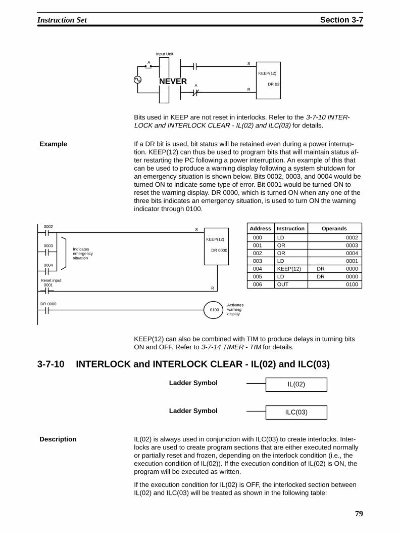
79
Input Unit
A
NEVER
S
R
KEEP(12)
DR 03A
Bits used in KEEP are not reset in interlocks. Refer to the 3-7-10 INTER-LOCK and INTERLOCK CLEAR - IL(02) and ILC(03) for details.
If a DR bit is used, bit status will be retained even during a power interrup-tion. KEEP(12) can thus be used to program bits that will maintain status af-ter restarting the PC following a power interruption. An example of this thatcan be used to produce a warning display following a system shutdown foran emergency situation is shown below. Bits 0002, 0003, and 0004 would beturned ON to indicate some type of error. Bit 0001 would be turned ON toreset the warning display. DR 0000, which is turned ON when any one of thethree bits indicates an emergency situation, is used to turn ON the warningindicator through 0100.
DR 0000
0100
0002
0003
0004
0001Reset input
Indicates emergencysituation
Activateswarningdisplay
Address Instruction Operands
000 LD 0002
001 OR 0003
002 OR 0004
003 LD 0001
004 KEEP(12) DR 0000
005 LD DR 0000
006 OUT 0100
S
R
KEEP(12)
DR 0000
KEEP(12) can also be combined with TIM to produce delays in turning bitsON and OFF. Refer to 3-7-14 TIMER - TIM for details.
3-7-10 INTERLOCK and INTERLOCK CLEAR - IL(02) and ILC(03)
Ladder Symbol IL(02)
Ladder Symbol ILC(03)
IL(02) is always used in conjunction with ILC(03) to create interlocks. Inter-locks are used to create program sections that are either executed normallyor partially reset and frozen, depending on the interlock condition (i.e., theexecution condition of IL(02)). If the execution condition of IL(02) is ON, theprogram will be executed as written.
If the execution condition for IL(02) is OFF, the interlocked section betweenIL(02) and ILC(03) will be treated as shown in the following table:
Example
Description
Instruction Set Section 3-7

80
Instruction Treatment
OUT and OUT NOT Designated bit turned OFF.
TIM, TIMM(20), TIMH(21), ATIM(22),ATM1(25), and ATM2(26)
Reset.
CNT, RDM(23), and CNTH(24) Frozen and PV maintained.
KEEP(12) Bit status maintained.
DIFU(10) and DIFD(11) Not executed (see below).
All others Not executed.
IL(02) and ILC(03) do not necessarily have to be used in pairs. IL(02) can beused several times in a row, with each IL(02) creating an interlocked sectionthrough the next ILC(03). ILC(03) cannot be used unless there is at least oneIL(02) between it and any previous ILC(03).
Changes in the execution condition for a DIFU(10) or DIFD(11) are not re-corded if the DIFU(10) or DIFD(11) is in an interlocked section and the ex-ecution condition for the IL(02) is OFF. When DIFU(10) or DIFD(11) is execu-tion in an interlocked section immediately after the execution condition for theIL(02) has gone ON, the execution condition for the DIFU(10) or DIFD(11)will be compared to the execution condition that existed before the interlockbecame effective (i.e., before the interlock condition for IL(02) went OFF).The ladder diagram and bit status changes for this are shown below. Theinterlock is in effect while bit 0000 is OFF. Notice that bit 0215 is not turnedON at the point labeled A even though 0001 has turned OFF and then backON.
0000
IL(02)
DIFU(10) 0215
ILC(03)
0001
0000
0001
ON
OFF
ON
OFF
0215ON
OFF
A
Address Instruction Operands
000 LD 0000
001 IL(02)
002 LD 0001
003 DIFU(10) 0215
004 ILC(03)
There must be an ILC(03) following any one or more IL(02).
Although as many IL(02) instructions as necessary can be used with oneILC(03), ILC(03) instructions cannot be used consecutively without at leastone IL(02) in between. Whenever a ILC(03) is executed, all interlocks be-tween the active ILC(03) and the preceding ILC(03) are cleared.
STEP(04) and SNXT(05) cannot be used between the INTERLOCK and IN-TERLOCK CLEAR instructions.
There are no flags affected by these instructions.
DIFU(10) and DIFD(11) inInterlocks
Precautions
Flags
Instruction Set Section 3-7
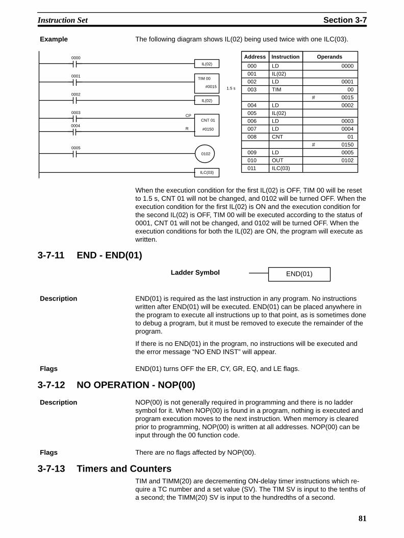
81
The following diagram shows IL(02) being used twice with one ILC(03).
0000
0001
ILC(03)
IL(02)
0005
0003
0002
IL(02)
0102
CP
R
CNT 01
#01500004
Address Instruction Operands
000 LD 0000
001 IL(02)
002 LD 0001
003 TIM 00
# 0015
004 LD 0002
005 IL(02)
006 LD 0003
007 LD 0004
008 CNT 01
# 0150
009 LD 0005
010 OUT 0102
011 ILC(03)
TIM 00
#0015 1.5 s
When the execution condition for the first IL(02) is OFF, TIM 00 will be resetto 1.5 s, CNT 01 will not be changed, and 0102 will be turned OFF. When theexecution condition for the first IL(02) is ON and the execution condition forthe second IL(02) is OFF, TIM 00 will be executed according to the status of0001, CNT 01 will not be changed, and 0102 will be turned OFF. When theexecution conditions for both the IL(02) are ON, the program will execute aswritten.
3-7-11 END - END(01)
Ladder Symbol END(01)
END(01) is required as the last instruction in any program. No instructionswritten after END(01) will be executed. END(01) can be placed anywhere inthe program to execute all instructions up to that point, as is sometimes doneto debug a program, but it must be removed to execute the remainder of theprogram.
If there is no END(01) in the program, no instructions will be executed andthe error message “NO END INST” will appear.
END(01) turns OFF the ER, CY, GR, EQ, and LE flags.
3-7-12 NO OPERATION - NOP(00)
NOP(00) is not generally required in programming and there is no laddersymbol for it. When NOP(00) is found in a program, nothing is executed andprogram execution moves to the next instruction. When memory is clearedprior to programming, NOP(00) is written at all addresses. NOP(00) can beinput through the 00 function code.
There are no flags affected by NOP(00).
3-7-13 Timers and CountersTIM and TIMM(20) are decrementing ON-delay timer instructions which re-quire a TC number and a set value (SV). The TIM SV is input to the tenths ofa second; the TIMM(20) SV is input to the hundredths of a second.
Example
Description
Flags
Description
Flags
Instruction Set Section 3-7

82
TIMH(21) is a decrementing ON-delay timer instruction which requires an SV,The SV is input to the thousandths of a second.
ATIM(22) is a decrementing ON-delay timer with a hardware adjustment forthe SV. On the SP16 and SP20, the hardware adjustment is the same forboth ATIM(22) and ATM1(25).
ATM1(25) and ATM2(26) are available with the SP16 and SP20 only. LikeATIM(22), they are decrementing ON-delay timers and the SV can be set byhardware adjustments on the front of the CPU. Unlike ATIM(22), the SV canalso be set in a word.
CNT is a decrementing counter instruction and RDM(23) is a reversible drumcounter instruction. Both require a TC number and a SV. Both are also con-nected to multiple instruction lines which serve as an input signal(s), a reset,and for RDM(23), an up/down input. RDM(23) also requires specification ofthe first word in the results table.
CNTH(24) is a high-speed incrementing counter that is available with theSP16 and SP20 only. It can count pulses as fast as 3.3 kHz.
Any one TC number cannot be defined twice, i.e., once it has been used asthe definer in any of the timer or counter instructions, it cannot be usedagain. Once defined, TC numbers can be used as many times as required asoperands in instructions.
TC numbers run from 00 through 15. No prefix is required when using a TCnumber as a definer in a timer or counter instruction. Once defined as a tim-er, a TC number can be prefixed with TIM for use as an operand in certaininstructions. The TIM prefix is used regardless of the timer instruction thatwas used to define the timer. Once defined as a counter, a TC number canbe prefixed with CNT for use as an operand in certain instructions. The CNTis also used regardless of the counter instruction that was used to define thecounter.
TC numbers can be designated as operands that require either bit or worddata. When designated as an operand that requires bit data, the TC numberaccesses a bit that functions as a ‘Completion Flag’ that indicates when thetime/count has expired, i.e., the bit, which is normally OFF, will turn ON whenthe designated SV has expired. When designated as an operand that re-quires word data, the TC number accesses a memory location that holds thepresent value (PV) of the timer or counter. The PV of a timer or counter canthus be used as an operand in CMP(32), or any other instruction for whichthe TC area is allowed. This is done by designating the TC number used todefine that timer or counter to access the memory location that holds the PV.
TC numbers TC 11 through TC 15 (just TC 14 and TC 15 for the SP10) areassigned to specific instructions, as shown in the table below.
TC number Instruction Applicable PCs
TC 11 ANALOG TIMER 1, ATM1(25) SP16, SP20
TC 12 ANALOG TIMER 2, ATM2(26) SP16, SP20
TC 13 HIGH-SPEED COUNTER, CNTH(24) SP16, SP20
TC 14 HIGH-SPEED TIMER, TIMH(21) SP10, SP16, SP20
TC 15 ANALOG TIMER, ATIM(22) SP10, SP16, SP20
Note The present value of timers and counters can be monitored through the Pro-gramming Console. Refer to the Bit/TC Monitor and Multibit/TC Monitor oper-ations.
Instruction Set Section 3-7

83
3-7-14 TIMER - TIM
N: TC number
# (00 through 15)
Ladder Symbol
Definer Values
SV: Set value (BCD)
SP10: #
SP16, SP20: I/O, work, DR, LR, #
Operand Data AreasTIM N
SV
SV is between 000.0 and 999.9 seconds. The decimal point is not entered.
Each TC number can be used as the definer in only one timer or counter in-struction.
TC 11 through TC 15 should not be used in TIM if they are required for thespecific instruction to which they are assigned. Refer to the table on page 82.
A timer is activated when its execution condition goes ON and is reset (toSV) when the execution condition goes OFF. Once activated, TIM measuresin units of 0.1 second from the SV. TIM accuracy is +0.0/–0.1 second.
If the execution condition remains ON long enough for TIM to time down tozero, the Completion Flag for the TC number used will turn ON and will re-main ON until TIM is reset (i.e., until its execution condition is goes OFF).
The following figure illustrates the relationship between the execution condi-tion for TIM and the Completion Flag assigned to it.
Execution condition
Completion Flag
ON
OFF
ON
OFF
SV SV
Timers in interlocked program sections are reset when the execution condi-tion for IL(02) is OFF. Power interruptions also reset timers. If a timer that isnot reset under these conditions is desired, dedicated clock pulse bits can becounted to produce timers using CNT. Refer to 3-7-18 COUNTER - CNT fordetails.
Flags ER: The Error Flag (0311) will be turned ON when the SV is set in a word(SP16 and SP20 only) but the content of the indicated word is notBCD. The instruction will be executed, but operation will not be reli-able.
All of the following examples use OUT to control output bits. There is no rea-son, however, why these diagrams cannot be modified to control execution ofother instructions.
The following example shows two timers. Here, 0100 will be turned ON afterbit 0000 goes ON and stays ON for at least 15 seconds. When bit 0000 goes
Limitations
Description
Precautions
Examples
Example 1: Basic Application
Instruction Set Section 3-7

84
OFF, the timer will be reset and 0100 will be turned OFF. When 0001 goesON, TIM 01 is started. Bit 0101 is also turned ON when 0001 goes ON.When 20 seconds have expired, 0101 is turned OFF. This bit will also beturned OFF when TIM 01 is reset, regardless of whether or not SV has ex-pired.
0000
TIM 00
0001
TIM 01
0100
0101
Address Instruction Operands
000 LD 0000
001 TIM 00
# 0150
002 LD TIM 00
003 OUT 0100
004 LD 0001
005 TIM 01
# 0200
006 AND NOT TIM 01
007 OUT 0101
TIM 00
#0150
TIM 01
#0200
There are two ways to achieve timers that operate for longer than 999.9 sec-onds. One method is to program consecutive timers, with the CompletionFlag of each timer used to activate the next timer. A simple example with two900.0-second (15-minute) timers combined to functionally form a 30-minutetimer.
0000
TIM 01
TIM 02
0100
Address Instruction Operands
000 LD 0000
001 TIM 01
# 9000
002 LD TIM 01
003 TIM 02
# 9000
004 LD TIM 02
005 OUT 0100
TIM 01
#9000
TIM 02
#9000
900.0 s
900.0 s
In this example, bit 0100 will be turned ON 30 minutes after bit 0000 goesON.
TIM can also be combined with CNT or CNT can be used to count dedicatedclock pulse bits to produce longer timers. An example is provided in 3-7-18COUNTER - CNT.
TIM can be combined with KEEP(12) to delay turning a bit ON and OFF inreference to a desired execution condition. KEEP(12) is described 3-7-9KEEP - KEEP(12).
To create delays, the Completion Flags for two TIM are used to determinethe execution conditions for setting and reset the bit designated forKEEP(12). The bit whose manipulation is to be delayed is used in KEEP(12).Turning ON and OFF the bit designated for KEEP(12) is thus delayed by theSV for the two TIM. The two SV could naturally be the same if desired.
In the following example, 0100 would be turned ON 5.0 seconds after 0000goes ON and then turned OFF 3.0 seconds after 0000 goes OFF. It is neces-sary to use both 0100 and 0000 to determine the execution condition for TIM02; 0000 in a normally closed condition is necessary to reset TIM 02 when0000 goes ON and 0100 is necessary to activate TIM 02 (when 0000 isOFF).
Example 2: Extended Timers
Example 3: ON/OFF Delays
Instruction Set Section 3-7
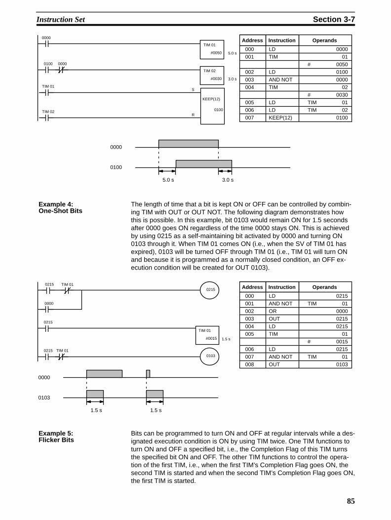
85
0000
0100 0000
TIM 01
TIM 02
0000
0100
5.0 s 3.0 s
Address Instruction Operands
000 LD 0000
001 TIM 01
# 0050
002 LD 0100
003 AND NOT 0000
004 TIM 02
# 0030
005 LD TIM 01
006 LD TIM 02
007 KEEP(12) 0100
TIM 01
#0050
TIM 02
#0030
S
R
KEEP(12)
0100
5.0 s
3.0 s
The length of time that a bit is kept ON or OFF can be controlled by combin-ing TIM with OUT or OUT NOT. The following diagram demonstrates howthis is possible. In this example, bit 0103 would remain ON for 1.5 secondsafter 0000 goes ON regardless of the time 0000 stays ON. This is achievedby using 0215 as a self-maintaining bit activated by 0000 and turning ON0103 through it. When TIM 01 comes ON (i.e., when the SV of TIM 01 hasexpired), 0103 will be turned OFF through TIM 01 (i.e., TIM 01 will turn ONand because it is programmed as a normally closed condition, an OFF ex-ecution condition will be created for OUT 0103).
0000
TIM 010215
0215
0215 TIM 01
0215
0103
0000
0103
1.5 s 1.5 s
Address Instruction Operands
000 LD 0215
001 AND NOT TIM 01
002 OR 0000
003 OUT 0215
004 LD 0215
005 TIM 01
# 0015
006 LD 0215
007 AND NOT TIM 01
008 OUT 0103
TIM 01
#0015 1.5 s
Bits can be programmed to turn ON and OFF at regular intervals while a des-ignated execution condition is ON by using TIM twice. One TIM functions toturn ON and OFF a specified bit, i.e., the Completion Flag of this TIM turnsthe specified bit ON and OFF. The other TIM functions to control the opera-tion of the first TIM, i.e., when the first TIM’s Completion Flag goes ON, thesecond TIM is started and when the second TIM’s Completion Flag goes ON,the first TIM is started.
Example 4: One-Shot Bits
Example 5: Flicker Bits
Instruction Set Section 3-7
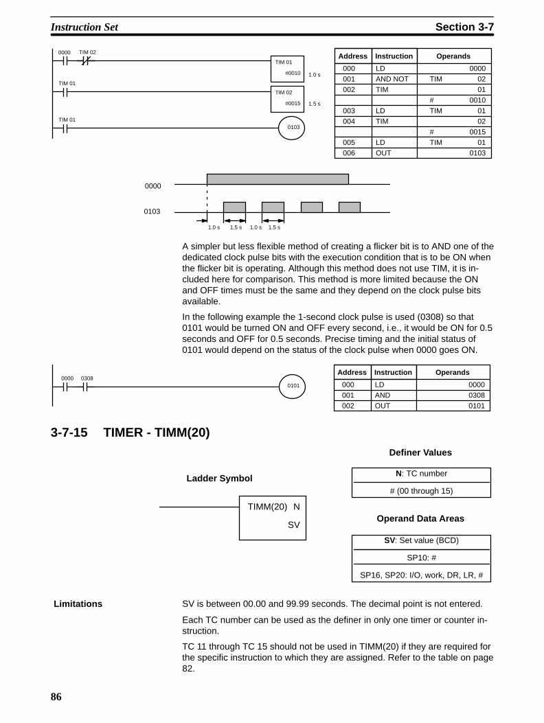
86
0000
TIM 01
TIM 010103
0000
0103
1.5 s1.0 s 1.5 s1.0 s
Address Instruction Operands
000 LD 0000
001 AND NOT TIM 02
002 TIM 01
# 0010
003 LD TIM 01
004 TIM 02
# 0015
005 LD TIM 01
006 OUT 0103
TIM 02
#0015
TIM 01
#0010 1.0 s
1.5 s
TIM 02
A simpler but less flexible method of creating a flicker bit is to AND one of thededicated clock pulse bits with the execution condition that is to be ON whenthe flicker bit is operating. Although this method does not use TIM, it is in-cluded here for comparison. This method is more limited because the ONand OFF times must be the same and they depend on the clock pulse bitsavailable.
In the following example the 1-second clock pulse is used (0308) so that0101 would be turned ON and OFF every second, i.e., it would be ON for 0.5seconds and OFF for 0.5 seconds. Precise timing and the initial status of0101 would depend on the status of the clock pulse when 0000 goes ON.
0000 03080101
Address Instruction Operands
000 LD 0000
001 AND 0308
002 OUT 0101
3-7-15 TIMER - TIMM(20)
N: TC number
# (00 through 15)
Ladder Symbol
Definer Values
SV: Set value (BCD)
SP10: #
SP16, SP20: I/O, work, DR, LR, #
Operand Data AreasTIMM(20) N
SV
SV is between 00.00 and 99.99 seconds. The decimal point is not entered.
Each TC number can be used as the definer in only one timer or counter in-struction.
TC 11 through TC 15 should not be used in TIMM(20) if they are required forthe specific instruction to which they are assigned. Refer to the table on page82.
Limitations
Instruction Set Section 3-7
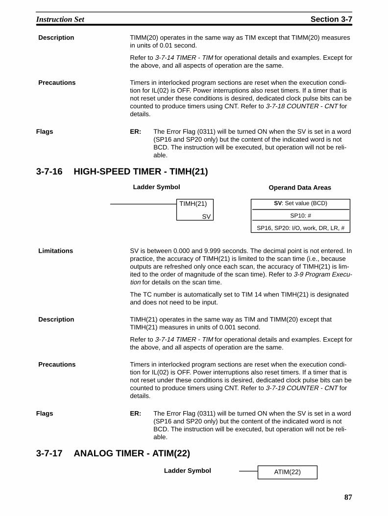
87
TIMM(20) operates in the same way as TIM except that TIMM(20) measuresin units of 0.01 second.
Refer to 3-7-14 TIMER - TIM for operational details and examples. Except forthe above, and all aspects of operation are the same.
Timers in interlocked program sections are reset when the execution condi-tion for IL(02) is OFF. Power interruptions also reset timers. If a timer that isnot reset under these conditions is desired, dedicated clock pulse bits can becounted to produce timers using CNT. Refer to 3-7-18 COUNTER - CNT fordetails.
Flags ER: The Error Flag (0311) will be turned ON when the SV is set in a word(SP16 and SP20 only) but the content of the indicated word is notBCD. The instruction will be executed, but operation will not be reli-able.
3-7-16 HIGH-SPEED TIMER - TIMH(21)
Ladder Symbol
TIMH(21)
SV
SV: Set value (BCD)
SP10: #
SP16, SP20: I/O, work, DR, LR, #
Operand Data Areas
SV is between 0.000 and 9.999 seconds. The decimal point is not entered. Inpractice, the accuracy of TIMH(21) is limited to the scan time (i.e., becauseoutputs are refreshed only once each scan, the accuracy of TIMH(21) is lim-ited to the order of magnitude of the scan time). Refer to 3-9 Program Execu-tion for details on the scan time.
The TC number is automatically set to TIM 14 when TIMH(21) is designatedand does not need to be input.
TIMH(21) operates in the same way as TIM and TIMM(20) except thatTIMH(21) measures in units of 0.001 second.
Refer to 3-7-14 TIMER - TIM for operational details and examples. Except forthe above, and all aspects of operation are the same.
Timers in interlocked program sections are reset when the execution condi-tion for IL(02) is OFF. Power interruptions also reset timers. If a timer that isnot reset under these conditions is desired, dedicated clock pulse bits can becounted to produce timers using CNT. Refer to 3-7-19 COUNTER - CNT fordetails.
Flags ER: The Error Flag (0311) will be turned ON when the SV is set in a word(SP16 and SP20 only) but the content of the indicated word is notBCD. The instruction will be executed, but operation will not be reli-able.
3-7-17 ANALOG TIMER - ATIM(22)
Ladder Symbol ATIM(22)
Description
Precautions
Limitations
Description
Precautions
Instruction Set Section 3-7
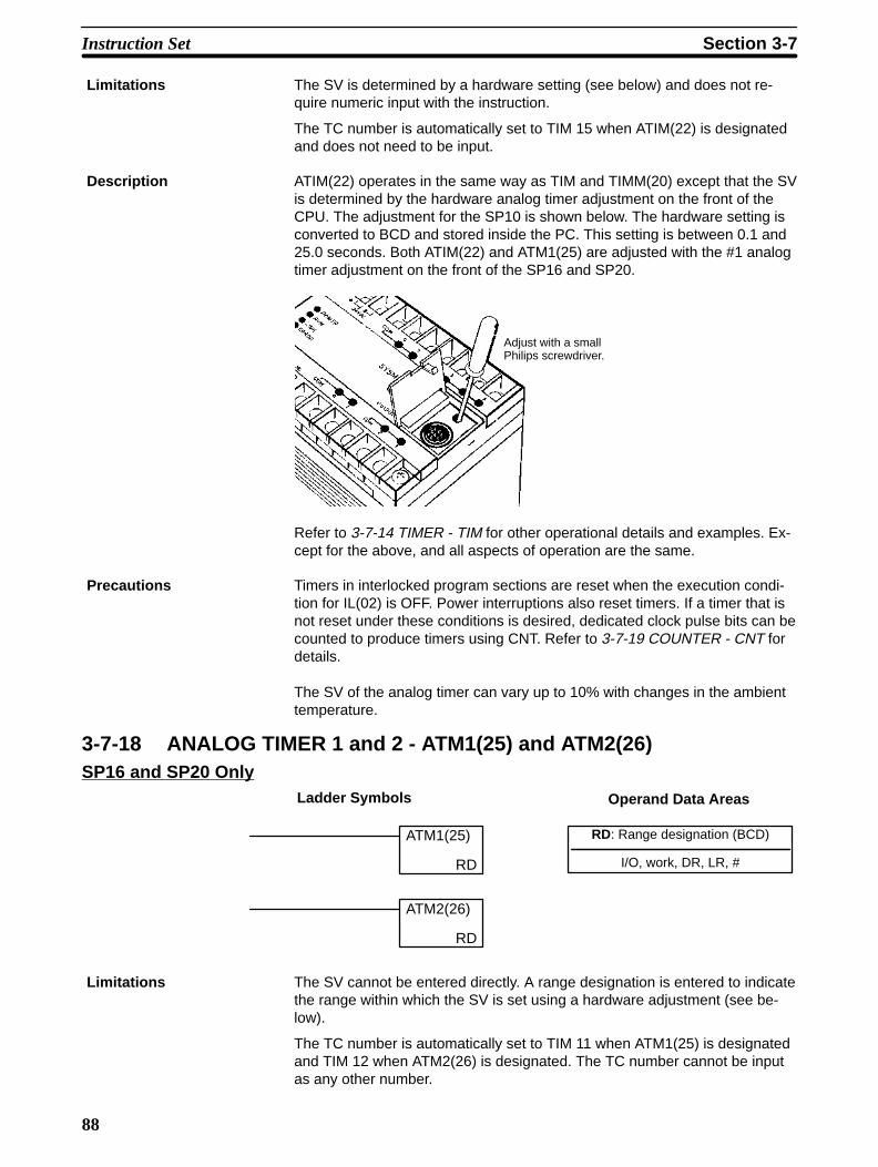
88
The SV is determined by a hardware setting (see below) and does not re-quire numeric input with the instruction.
The TC number is automatically set to TIM 15 when ATIM(22) is designatedand does not need to be input.
ATIM(22) operates in the same way as TIM and TIMM(20) except that the SVis determined by the hardware analog timer adjustment on the front of theCPU. The adjustment for the SP10 is shown below. The hardware setting isconverted to BCD and stored inside the PC. This setting is between 0.1 and25.0 seconds. Both ATIM(22) and ATM1(25) are adjusted with the #1 analogtimer adjustment on the front of the SP16 and SP20.
Adjust with a small Philips screwdriver.
Refer to 3-7-14 TIMER - TIM for other operational details and examples. Ex-cept for the above, and all aspects of operation are the same.
Timers in interlocked program sections are reset when the execution condi-tion for IL(02) is OFF. Power interruptions also reset timers. If a timer that isnot reset under these conditions is desired, dedicated clock pulse bits can becounted to produce timers using CNT. Refer to 3-7-19 COUNTER - CNT fordetails.
The SV of the analog timer can vary up to 10% with changes in the ambienttemperature.
3-7-18 ANALOG TIMER 1 and 2 - ATM1(25) and ATM2(26)SP16 and SP20 Only
Ladder Symbols
ATM1(25)
RD
RD: Range designation (BCD)
I/O, work, DR, LR, #
Operand Data Areas
ATM2(26)
RD
The SV cannot be entered directly. A range designation is entered to indicatethe range within which the SV is set using a hardware adjustment (see be-low).
The TC number is automatically set to TIM 11 when ATM1(25) is designatedand TIM 12 when ATM2(26) is designated. The TC number cannot be inputas any other number.
Limitations
Description
Precautions
Limitations
Instruction Set Section 3-7

89
ATM1(25) and ATM2(26) operate in the same way as TIM and TIMM(20) ex-cept that their SVs are determined by the #1 and #2 analog timer adjust-ments on the front of the CPU. The hardware setting is converted to BCDand stored in dedicated word 08. The ranges within which the hardware ad-justment operations is designated as the operand (RD) of the instruction.These designations are shown in the following table.
RD SV range
0000 1 to 250 seconds
0001 0.1 to 25.0 seconds
0002 0.01 to 2.50 seconds
RD can be designated either as a constant, or as the contents of a word bydesignated a word address.
Both ATIM(22) and ATM1(25) are adjusted with the #1 analog timer adjust-ment on the front of the SP16 and SP20. Although both of these instructionscan be used at the same time, their SVs cannot be adjusted independently,although the range of the set value for ATM1(25) can be controlled as de-scribed above. ATM2(26) is adjusted with the #2 analog timer adjustmentand can thus be set independently from other timers.
Refer to 3-7-14 TIMER - TIM for other operational details and examples. Ex-cept for the above, and all aspects of operation are the same.
Timers in interlocked program sections are reset when the execution condi-tion for IL(02) is OFF. Power interruptions also reset timers. If a timer not re-set under these conditions is desired, clock pulse bits can be counted to pro-duce timers using CNT. Refer to 3-7-19 COUNTER - CNT for details.
The SV of the analog timer can vary up to 10% with changes in the ambienttemperature.
Flags ER: The Error Flag (0311) will be turned ON when the RD contained in aword is not BCD. The instruction will be executed, but operation willnot be reliable.
3-7-19 COUNTER - CNT
N: TC number
# (00 through 15)
Ladder Symbol
Definer Values
CP
R
CNT N
SV
SV: Set value (BCD)
SP10: #
SP16, SP20: I/O, work, DR, LR, #
Operand Data Areas
Each TC number can be used as the definer in only one timer or counter in-struction.
TC 11 through TC 15 should not be used in CNT if they are required for thespecific instruction to which they are assigned. Refer to the table on page 82.
Description
Precautions
Limitations
Instruction Set Section 3-7

90
CNT is used to count down from SV when the execution condition on thecount pulse, CP, goes from OFF to ON, i.e., the present value (PV) will bedecremented by one whenever CNT is executed with an ON execution condi-tion for CP and the execution condition was OFF for the last execution. If theexecution condition has not changed or has changed from ON to OFF, thePV of CNT will not be changed. The Completion Flag for a counter is turnedON when the PV reaches zero and will remain ON until the counter is reset.
CNT is reset with a reset input, R. When R goes from OFF to ON, the PV isreset to SV. The PV will not be decremented while R is ON. Counting downfrom SV will begin again when R goes OFF. The PV for CNT will not be resetin interlocked program sections or by power interruptions.
Changes in execution conditions, the Completion Flag, and the PV are illus-trated below. PV line height is meant only to indicate changes in the PV.
Execution condition on count pulse (CP)
Execution condition on reset (R)
ON
OFF
ON
OFF
Completion FlagON
OFF
PVSV
SV – 1
SV – 2
0002
0001
0000
SV
Flags ER: The Error Flag (0311) will be turned ON when the SV is contained ina word (SP16 and SP20 only) but the content of the indicated word isnot BCD. The instruction will be executed, but operation will not bereliable.
In the following example, the PV will be decremented whenever both 0000and 0001 are ON provided that 0002 is OFF and either 0000 or 0001 wasOFF the last time CNT 04 was executed. When 150 pulses have beencounted down (i.e., when PV reaches zero), 0103 will be turned ON.
0000CP
R
CNT 04
#01500002
0001
0103
CNT 04
Address Instruction Operands
000 LD 0000
001 AND 0001
002 LD 0002
003 CNT 04
# 0150
004 LD CNT 04
005 OUT 0103
Here, 0000 can be used to control when CNT is operative and 0001 can beused as the bit whose OFF to ON changes are being counted.
The above CNT can be modified to restart from SV each time power isturned ON to the PC. This is done by using the First Scan Flag (0410) to re-set CNT as shown below.
Description
Example 1: Basic Application
Example 2: Reset for PowerInterruptions
Instruction Set Section 3-7

91
0000CP
R
CNT 04
#01500002
0001
0103
CNT 04
0410
Address Instruction Operands
000 LD 0000
001 AND 0001
002 LD 0002
003 OR 0410
004 CNT 04
# 0150
005 LD CNT 04
006 OUT 0103
Counters that can count past 9,999 can be programmed by using one CNT tocount the number of times another CNT has counted to zero from SV.
In the following example, 0000 is used to control when CNT 01 operates.CNT 01, when 0000 is ON, counts down the number of OFF to ON changesin 0001. CNT 01 is reset by its Completion Flag, i.e., it starts counting againas soon as its PV reaches zero. CNT 02 counts the number of times theCompletion Flag for CNT 01 goes ON. Bit 0002 serves as a reset for the en-tire extended counter, resetting both CNT 01 and CNT 02 when it is OFF.The Completion Flag for CNT 02 is also used to reset CNT 01 to inhibit CNT01 operation, once SV for CNT 02 has been reached, until the entire ex-tended counter is reset via 0002.
Because in this example the SV for CNT 01 is 100 and the SV for CNT 02 is200, the Completion Flag for CNT 02 turns ON when 100 x 200 or 20,000OFF to ON changes have been counted in 0001. This would result in 0103being turned ON.
0103
CP
R
CNT 01
#0100
CP
R
CNT 02
#0200
CNT 01
0002
CNT 02
0000 0001
0002
CNT 01
CNT 02
Address Instruction Operands
000 LD 0000
001 AND 0001
002 LD NOT 0002
003 OR CNT 01
004 OR CNT 02
005 CNT 01
# 0100
006 LD CNT 01
007 LD NOT 0002
008 CNT 02
# 0200
009 LD CNT 02
010 OUT 0103
CNT can be used in sequence as many times as required to produce count-ers capable of counting any desired values.
CNT can be used to create extended timers in two ways: by combining TIMwith CNT and by counting dedicated clock pulse bits.
In the following example, CNT 02 counts the number of times TIM 01 reach-es zero from its SV. The Completion Flag for TIM 01 is used to reset TIM 01so that is runs continuously and CNT 02 counts the number of times theCompletion Flag for TIM 01 goes ON (CNT 02 would be executed once eachtime between when the Completion Flag for TIM 01 goes ON and TIM 01 is
Example 3: ExtendedCounter
Example 4: Extended Timers
Instruction Set Section 3-7

92
reset by its Completion Flag). TIM 01 is also reset by the Completion Flag forCNT 02 so that the extended timer would not start again until CNT 02 wasreset by 0001, which serves as the reset for the entire extended timer.
Because in this example the SV for TIM 01 is 5.0 seconds and the SV forCNT 02 is 100, the Completion Flag for CNT 02 turns ON when 5 seconds x100 times, i.e., 500 seconds (or 8 minutes and 20 seconds) have expired.This would result in bit 0100 being turned ON.
0000 TIM 01 CNT 02
TIM 01
0001
CNT 02
0100
CP
R
CNT 02
#0100
Address Instruction Operands
000 LD 0000
001 AND NOT TIM 01
002 AND NOT CNT 02
003 TIM 01
# 0050
004 LD TIM 01
005 LD 0001
006 CNT 02
# 0100
007 LD CNT 02
008 OUT 0100
TIM 01
#0050
In the following example, CNT 01 counts the number of times the 1-secondclock pulse bit (0308) goes from OFF to ON. Here again, 0000 is used tocontrol the times when CNT is operating.
Because in this example the SV for CNT 01 is 700, the Completion Flag forCNT 02 turns ON when 1 second x 700 times, or 11 minutes and 40 secondshave expired. This would result in 0102 being turned ON.
CP
R
CNT 01
#0700
0000 0308
0001
CNT 010102
Address Instruction Operands
000 LD 0000
001 AND 0308
002 LD NOT 0001
003 CNT 01
# 0700
004 LD CNT 01
005 OUT 0102
3-7-20 REVERSIBLE DRUM COUNTER -RDM(23)
N: TC number
# (00 to 15)
Ladder Symbol
Definer Values
St: Starting table word
DR
Operand Data Areas
II
DI
RI
RDM(23) N
St
R
R : Results word
Output bits, work bits, DR, LR
St must be between 0000 and 0003. All unused bits in R can be used aswork bits.
Limitations
Instruction Set Section 3-7
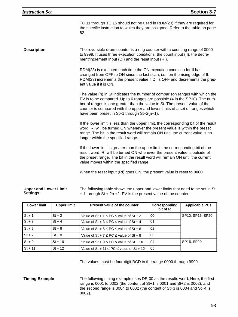
93
TC 11 through TC 15 should not be used in RDM(23) if they are required forthe specific instruction to which they are assigned. Refer to the table on page82.
The reversible drum counter is a ring counter with a counting range of 0000to 9999. It uses three execution conditions, the count input (II), the decre-ment/increment input (DI) and the reset input (RI).
RDM(23) is executed each time the ON execution condition for II haschanged from OFF to ON since the last scan, i.e., on the rising edge of II.RDM(23) increments the present value if DI is OFF and decrements the pres-ent value if it is ON.
The value (n) in St indicates the number of comparison ranges with which thePV is to be compared. Up to 6 ranges are possible (4 in the SP10). The num-ber of ranges is one greater than the value in St. The present value of thecounter is compared with the upper and lower limits of a set of ranges whichhave been preset in St+1 through St+2(n+1).
If the lower limit is less than the upper limit, the corresponding bit of the resultword, R, will be turned ON whenever the present value is within the presetrange. The bit in the result word will remain ON until the current value is nolonger within the specified range.
If the lower limit is greater than the upper limit, the corresponding bit of theresult word, R, will be turned ON whenever the present value is outside ofthe preset range. The bit in the result word will remain ON until the currentvalue moves within the specified range.
When the reset input (RI) goes ON, the present value is reset to 0000.
The following table shows the upper and lower limits that need to be set in St+ 1 through St + 2n +2. PV is the present value of the counter.
Lower limit Upper limit Present value of the counter Correspondingbit of R
Applicable PCs
St + 1 St + 2 Value of St + 1 ≤ PC ≤ value of St + 2 00 SP10, SP16, SP20
St + 3 St + 4 Value of St + 3 ≤ PC ≤ value of St + 4 01
St + 5 St + 6 Value of St + 5 ≤ PC ≤ value of St + 6 02
St + 7 St + 8 Value of St + 7 ≤ PC ≤ value of St + 8 03
St + 9 St + 10 Value of St + 9 ≤ PC ≤ value of St + 10 04 SP16, SP20
St + 11 St + 12 Value of St + 11 ≤ PC ≤ value of St + 12 05
The values must be four-digit BCD in the range 0000 through 9999.
The following timing example uses DR 00 as the results word. Here, the firstrange is 0001 to 0002 (the content of St+1 is 0001 and St+2 is 0002), andthe second range is 0004 to 0002 (the content of St+3 is 0004 and St+4 is0002).
Description
Upper and Lower LimitSettings
Timing Example
Instruction Set Section 3-7

94
DR 0000Limits: 0001 to 0002
Count input (II)
0000 0001 0002 0003 0004 0005 0004 0003 0002 0001 0000 9999 9998 9997 0000 00000000
DR 0001Limits: 0004 to 0002
Present value
Reset input (RI)
Decrement/increment input (DI))
3-7-21 HIGH-SPEED COUNTER - CNTH(24)
SP16 and SP20 Only
SV: Set value (BCD)
I/O, work, DR, LR, #
Operand Data AreasLadder Symbol
SI
R
CNTH(24) N
SV
The TC number is automatically set to CNT 13, the count pulse (CP) to inputbit 0000, and the hard reset input (R) to input bit 0001 when CNTH(24) isdesignated. Inputs 0000 and 0001 cannot be used as normal input terminalswhen CNTH(24) is being used.
CNTH(24) is a high-speed incrementing counter. The present value (PV) be-gins at 0000 and will be incremented by one whenever CP (input bit 0000)goes from OFF to ON as long as the start input condition (SI) is ON and thereset input (R) is OFF. The start input and reset input conditions are enteredwith LD before CNTH(24) is entered. The Completion Flag, CNT 13, is turnedON when the PV reaches the SV and will remain ON for one scan only.When the SV is reached, the PC will be automatically reset to zero.
The maximum counter value can be set by setting the SV to 0000 rather thanto 9999, i.e., the counter will count to 10,000 when the SV is set to 0000.
CNTH(24) is reset with R. When R goes from OFF to ON, the PV is reset tozero. The PV will not be incremented while R is ON. Counting from zero willbegin again when R goes OFF. The PV for CNT 13 will not be reset in inter-locked program sections or by power interruptions.
CNTH(24) counting is enabled with SI. When SI is OFF, the PV is notchanged even if R is OFF and CP goes from OFF to ON. Counting will re-sume when SI is turned ON again.
The count pulse for CNTH(24) is input bit 0000 and the hard reset input isinput bit 0001. The count signal must be at least 150 µs (3.3 kHz) wide and
Limitations
Description
Instruction Set Section 3-7

95
have a duty factor of 1:1, and the reset signal must have an ON time of atleast 250 µs, as shown below.
150µs
Input0000
150µs
250 µs min.
Input0001
Inputs 0000 and 0001 can be used as normal inputs when CNTH(24) is notused, but the input signals must be 1 kHz max. (500 µs wide min.).
Do not use the 0001 reset input in combination with other input bits in thereset execution condition.
0002SI
R
CNTH(24)
CNT13
#01500003
0004
0001
Incorrect0002
SI
R
CNTH(24)
CNT13
#01500001
Correct
0002SI
R
CNTH(24)
CNT13
#01500003 00010004
0002SI
R
CNTH(24)
CNT13
#01500003
0004
Flags ER: The Error Flag (0311) will be turned ON when the SV is not BCD.The instruction will be executed, but operation will not be reliable.
In the following example, the PV will be incremented whenever the countpulse, 0000, goes from OFF to ON provided that the start input, 0002, is ONand the reset input, 2003 is OFF. When 150 pulses have been counted (i.e.,when the PV reaches the SV), the Completion Flag, CNT 13, and 0101 willbe turned ON.
0002SI
R
CNTH(24)
CNT13
#01502003
0101
CNT 13
Address Instruction Operands
000 LD 0002
001 LD 2003
002 CNTH(24) CNT 13
# 0150
003 LD CNT 13
004 OR 0101
005 OUT 0101
0101
Precautions
Example 1: Basic Application
Instruction Set Section 3-7
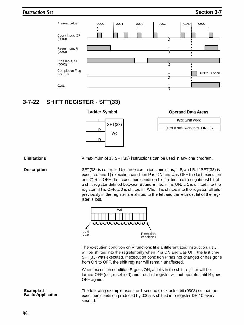
96
Completion FlagCNT 13
Count input, CP(0000)
0000 0001 0002 0003 0000
0101
Present value
Reset input, R(2003)
Start input, SI(0002)
0149
ON for 1 scan
3-7-22 SHIFT REGISTER - SFT(33)
Wd: Shift word
Output bits, work bits, DR, LR
Operand Data AreasLadder Symbol
I
PSFT(33)
Wd
R
A maximum of 16 SFT(33) instructions can be used in any one program.
SFT(33) is controlled by three execution conditions, I, P, and R. If SFT(33) isexecuted and 1) execution condition P is ON and was OFF the last executionand 2) R is OFF, then execution condition I is shifted into the rightmost bit ofa shift register defined between St and E, i.e., if I is ON, a 1 is shifted into theregister; if I is OFF, a 0 is shifted in. When I is shifted into the register, all bitspreviously in the register are shifted to the left and the leftmost bit of the reg-ister is lost.
Execution condition I
Lostdata
Wd
The execution condition on P functions like a differentiated instruction, i.e., Iwill be shifted into the register only when P is ON and was OFF the last timeSFT(33) was executed. If execution condition P has not changed or has gonefrom ON to OFF, the shift register will remain unaffected.
When execution condition R goes ON, all bits in the shift register will beturned OFF (i.e., reset to 0) and the shift register will not operate until R goesOFF again.
The following example uses the 1-second clock pulse bit (0308) so that theexecution condition produced by 0005 is shifted into register DR 10 everysecond.
Limitations
Description
Example 1: Basic Application
Instruction Set Section 3-7
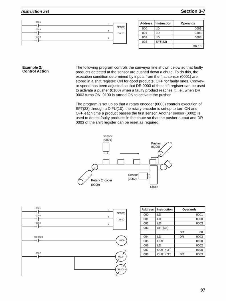
97
I
P
SFT(33)
DR 10
R
0005
0308
0008
Address Instruction Operands
000 LD 0005
001 LD 0308
002 LD 0008
003 SFT(33)
DR 10
The following program controls the conveyor line shown below so that faultyproducts detected at the sensor are pushed down a chute. To do this, theexecution condition determined by inputs from the first sensor (0001) arestored in a shift register: ON for good products; OFF for faulty ones. Convey-or speed has been adjusted so that DR 0003 of the shift register can be usedto activate a pusher (0100) when a faulty product reaches it, i.e., when DR0003 turns ON, 0100 is turned ON to activate the pusher.
The program is set up so that a rotary encoder (0000) controls execution ofSFT(33) through a DIFU(10), the rotary encoder is set up to turn ON andOFF each time a product passes the first sensor. Another sensor (0002) isused to detect faulty products in the chute so that the pusher output and DR0003 of the shift register can be reset as required.
Sensor
Chute
(0002)
(0100)
Sensor(0001)
Rotary Encoder(0000)
Pusher
I
P
SFT(33)
DR 00
R
0001
0000
0003
0100
DR 0003
0002
DR 0003
0100
Address Instruction Operands
000 LD 0001
001 LD 0000
002 LD 0003
003 SFT(33)
DR 00
004 LD DR 0003
005 OUT 0100
006 LD 0002
007 OUT NOT 0100
008 OUT NOT DR 0003
Example 2: Control Action
Instruction Set Section 3-7

98
3-7-23 MOVE - MOV(30)
S: Source word
I/O, work, dedicated (03 only), DR, LR, TC, #
D: Destination word
Output bits, work bits, DR, LR
Ladder Symbol Operand Data Areas
MOV(30)
S
D
When the execution condition is OFF, MOV(30) is not executed. When theexecution condition is ON, MOV(30) copies the content of S to D.
Source word Destination word
Bit status not changed.
MOV(30) will be executed every scan unless programmed with DIFU(10) orDIFD(11).
Flags ER: Indirectly addressed DR word is non-existent. (Content of *DR wordis not BCD, or the DR area boundary has been exceeded.)
EQ: ON when all zeros are transferred to D.
3-7-24 MOVE NOT - MVN(31)
S: Source word
I/O, work, dedicated (03 only), DR, LR, TC, #
D: Destination word
Output bits, work bits, DR, LR
Ladder Symbol Operand Data Areas
MVN(31)
S
D
When the execution condition is OFF, MVN(31) is not executed. When theexecution condition is ON, MVN(31) transfers the complement of S to D, i.e.,for each ON bit in S, the corresponding bit in D is turned OFF, and for eachOFF bit in S, the corresponding bit in D is turned ON.
Source word Destination word
Bit status inverted.
MVN(31) will be executed every scan unless programmed with DIFU(10) orDIFD(11).
ER: Indirectly addressed DR word is non-existent. (Content of *DR wordis not BCD, or the DR area boundary has been exceeded.)
EQ: ON when all zeros are transferred to D.
Description
Precautions
Description
Precautions
Flags
Instruction Set Section 3-7

99
3-7-25 COMPARE - CMP(32)
Cp1: First compare word
I/O, work, dedicated (03 only), DR, LR, TC, #
Ladder Symbol Operand Data Areas
CMP(32)
Cp1
Cp2Cp2: Second compare word
I/O, work, dedicated (03 only), DR, LR, TC, #
When comparing a value to the PV of a timer or counter, the value must be inBCD.
When the execution condition is OFF, CMP(32) is not executed. When theexecution condition is ON, CMP(32) compares Cp1 and Cp2 and outputs theresult to the GR, EQ, and LE flags in the dedicated area.
Placing other instructions between CMP(32) and the operation which ac-cesses the EQ, LE, and GR flags may change the status of these flags. Besure to access them before the desired status is changed.
ER: Indirectly addressed DR word is non-existent. (Content of *DR wordis not BCD, or the DR area boundary has been exceeded.)
EQ: ON if Cp1 equals Cp2.
LE: ON if Cp1 is less than Cp2.
GR: ON if Cp1 is greater than Cp2.
The following example shows how to save the comparison result immediate-ly. If the content of 01 is greater than that of DR 09, 0100 is turned ON; if thetwo contents are equal, 0101 is turned ON; if content of 01 is less than that ofDR 09, 0102 is turned ON. In some applications, only one of the three OUTswould be necessary, making the use of TR 0 unnecessary. With this type of
Limitations
Description
Precautions
Flags
Example 1: Saving CMP(32) Results
Instruction Set Section 3-7

100
programming, 0100, 0101, and 0102 are changed only when CMP(32) is ex-ecuted.
CMP(32)
01
DR 09
03150100
03130102
0314
0101
Greater Than
Equal
Less Than
Address Instruction Operands Address Instruction Operands
000 LD 0000
001 IL(02)
002 CMP(32)
01
DR 09
003 LD 0315
004 OUT 0100
005 LD 0314
006 OUT 0101
007 LD 0313
008 OUT 0102
009 ILC(03)
0000
IL(02)
ILC(03)
The following example uses TIM, CMP(32), and the LE flag (0313) to pro-duce outputs at particular times in the timer’s countdown. The timer is startedby turning ON 0000. When 0000 is OFF, TIM 10 is reset and the second twoCMP(32)s are not executed (i.e., executed with OFF execution conditions).Output 0100 is produced after 100 seconds; output 0101, after 200 seconds;and output 0103, after 500 seconds.
#3000
CMP(32)
TIM 10
CMP(32)
TIM 10
#4000
0101
0103
0100
0313
0313
TIM 10
Output at100 s.
Output at200 s.
Output at500 s.
TIM 10
#5000
0000
IL(02)
ILC(03)
Example 2: Obtaining Indicationsduring Timer Operation
Instruction Set Section 3-7
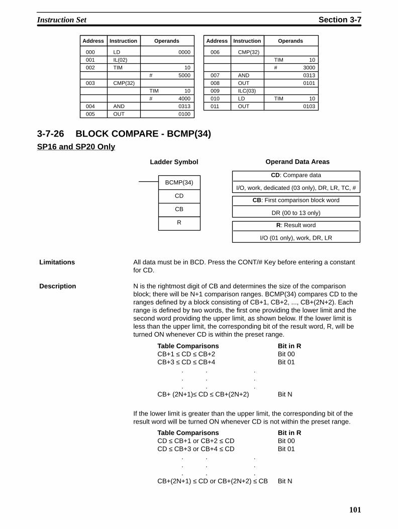
101
Address Instruction Operands Address Instruction Operands
000 LD 0000
001 IL(02)
002 TIM 10
# 5000
003 CMP(32)
TIM 10
# 4000
004 AND 0313
005 OUT 0100
006 CMP(32)
TIM 10
# 3000
007 AND 0313
008 OUT 0101
009 ILC(03)
010 LD TIM 10
011 OUT 0103
3-7-26 BLOCK COMPARE - BCMP(34)SP16 and SP20 Only
CD: Compare data
I/O, work, dedicated (03 only), DR, LR, TC, #
CB: First comparison block word
DR (00 to 13 only)
Ladder Symbol Operand Data Areas
R: Result word
I/O (01 only), work, DR, LR
BCMP(34)
CD
CB
R
All data must be in BCD. Press the CONT/# Key before entering a constantfor CD.
N is the rightmost digit of CB and determines the size of the comparisonblock; there will be N+1 comparison ranges. BCMP(34) compares CD to theranges defined by a block consisting of CB+1, CB+2, ..., CB+(2N+2). Eachrange is defined by two words, the first one providing the lower limit and thesecond word providing the upper limit, as shown below. If the lower limit isless than the upper limit, the corresponding bit of the result word, R, will beturned ON whenever CD is within the preset range.
Table Comparisons Bit in RCB+1 ≤ CD ≤ CB+2 Bit 00CB+3 ≤ CD ≤ CB+4 Bit 01
. . .
. . .
. . .CB+ (2N+1)≤ CD ≤ CB+(2N+2) Bit N
If the lower limit is greater than the upper limit, the corresponding bit of theresult word will be turned ON whenever CD is not within the preset range.
Table Comparisons Bit in RCD ≤ CB+1 or CB+2 ≤ CD Bit 00CD ≤ CB+3 or CB+4 ≤ CD Bit 01
. . .
. . .
. . .CB+(2N+1) ≤ CD or CB+(2N+2) ≤ CB Bit N
Limitations
Description
Instruction Set Section 3-7

102
If the content of CB or the table data are changed during execution, execu-tion will continue with the new values.
ER: Indirectly addressed DM word is non-existent. (Content of *DM wordis not BCD, or the DM area boundary has been exceeded.)
The following example shows the comparisons made and the results pro-vided for BCMP(34). Here, the comparison is made during each scan when0000 is ON. The rightmost digit of CB (DR 00) is 5, so the comparison blockis CB+1 to CB+(2N+2) or DR 01 to DR 12.
CB: DR 00 Lower limits Upper limits R: 01
DR 00 0005 DR 01 0000 DR 02 0100 0100 0
DR 03 0101 DR 04 0200 0101 0
DR 05 0201 DR 06 0300 0102 1
CD: 02 DR 07 0501 DR 08 0600 0103 0
DR 09 1401 DR 10 1500 0104 0
02 0210 DR 11 1501 DR 12 1600 0105 0
BCMP(34)
02
DR 00
01
00000
Comparison block: CB+1 toCB+(2N+2) or DR 01 to DR12.
Address Instruction Operands
000 LD 0000
001 BCMP(34)
02
DR 00
01
Compare data in 02 (which contains 0210).
3-7-27 CLEAR CARRY - CLC(44)
Ladder Symbol
CLC(44)
When the execution condition is OFF, CLC(44) is not executed.When the ex-ecution condition is ON, CLC(44) turns OFF CY (0312).
3-7-28 BCD ADD - ADD(40)
Au : Augend word (BCD)
I/O, work, dedicated (03 only), DR, LR, TC, #
Ad : Addend word (BCD)
I/O, work, dedicated (03 only), DR, LR, TC, #
Ladder Symbol
Operand Data Areas
R: Result word
Output bits, work bits, DR, LR
ADD(40)
Au
Ad
R
When the execution condition is OFF, ADD(40) is not executed. When theexecution condition is ON, ADD(40) adds the contents of Au, Ad, and CY,and places the result in R. CY will be set if the result is greater than 9999.
Flags
Example
Description
Instruction Set Section 3-7

103
Au + Ad + CY CY R
ER: Au and/or Ad is not BCD.Indirectly addressed DR word is non-existent. (Content of *DR wordis not BCD, or the DR area boundary has been exceeded.)
CY: ON when there is a carry in the result.EQ: ON when the result is 0.
If 0002 is ON, the program represented by the following diagram clears CYwith CLC(44), adds the content of LR 25 to a constant (6103), places the re-sult in DR 0100, and then moves either all zeros or 0001 into DR 0101 de-pending on the status of CY (0312). This ensures that any carry from the lastdigit is preserved in R+1 so that the entire result can be later handled aseight-digit data.
0002CLC(44)
ADD(40)
LR 25
#6103
DR 00
Address Instruction Operands
000 LD 0002
001 CLC(44)
002 AND(40)
LR 25
# 6103
DR 00
003 AND 0312
004 AND(40)
# 0000
# 0000
DR 01
ADD(40)
#0000
#0000
DR 01
0312
CY
3-7-29 BCD SUBTRACT - SUB(41)
Mi: Minuend word (BCD)
I/O, work, dedicated (03 only), DR, LR, TC, #
Su: Subtrahend word (BCD)
I/O, work, dedicated (03 only), DR, LR, TC, #
Ladder Symbol
Operand Data Areas
R: Result word
Output bits, work bits, DR, LR
SUB(41)
Mi
Su
R
When the execution condition is OFF, SUB(41) is not executed. When theexecution condition is ON, SUB(41) subtracts the contents of Su and CYfrom Mi, and places the result in R. If the result is negative, CY is set and the10’s complement of the actual result is placed in R. To convert the 10’s com-plement to the true result, subtract the content of R from zero (see examplebelow).
Mi – Su – CY CY R
ER: Mi and/or Su is not BCD.Indirectly addressed DR word is non-existent. (Content of *DR wordis not BCD, or the DR area boundary has been exceeded.)
CY: ON when the result is negative, i.e., when Mi is less than Su plus CY.EQ: ON when the result is 0.
Flags
Example
Description
Flags
Instruction Set Section 3-7
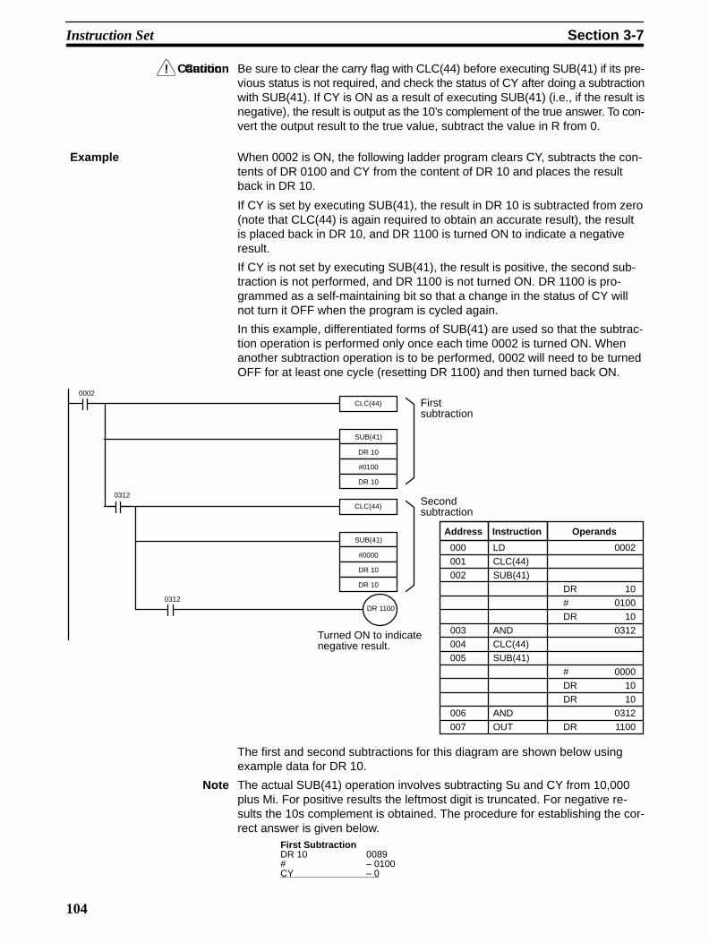
!
104
Caution Be sure to clear the carry flag with CLC(44) before executing SUB(41) if its pre-vious status is not required, and check the status of CY after doing a subtractionwith SUB(41). If CY is ON as a result of executing SUB(41) (i.e., if the result isnegative), the result is output as the 10’s complement of the true answer. To con-vert the output result to the true value, subtract the value in R from 0.
When 0002 is ON, the following ladder program clears CY, subtracts the con-tents of DR 0100 and CY from the content of DR 10 and places the resultback in DR 10.
If CY is set by executing SUB(41), the result in DR 10 is subtracted from zero(note that CLC(44) is again required to obtain an accurate result), the resultis placed back in DR 10, and DR 1100 is turned ON to indicate a negativeresult.
If CY is not set by executing SUB(41), the result is positive, the second sub-traction is not performed, and DR 1100 is not turned ON. DR 1100 is pro-grammed as a self-maintaining bit so that a change in the status of CY willnot turn it OFF when the program is cycled again.
In this example, differentiated forms of SUB(41) are used so that the subtrac-tion operation is performed only once each time 0002 is turned ON. Whenanother subtraction operation is to be performed, 0002 will need to be turnedOFF for at least one cycle (resetting DR 1100) and then turned back ON.
000 LD 0002
001 CLC(44)
002 SUB(41)
DR 10
# 0100
DR 10
003 AND 0312
004 CLC(44)
005 SUB(41)
# 0000
DR 10
DR 10
006 AND 0312
007 OUT DR 1100
CLC(44)
SUB(41)
DR 10
#0100
DR 10
CLC(44)
SUB(41)
#0000
DR 10
DR 10
0312DR 1100
0002
0312
First subtraction
Secondsubtraction
Turned ON to indicatenegative result.
Address Instruction Operands
The first and second subtractions for this diagram are shown below usingexample data for DR 10.
The actual SUB(41) operation involves subtracting Su and CY from 10,000plus Mi. For positive results the leftmost digit is truncated. For negative re-sults the 10s complement is obtained. The procedure for establishing the cor-rect answer is given below.
First SubtractionDR 10 0089# – 0100CY – 0
Caution
Example
Note
Instruction Set Section 3-7
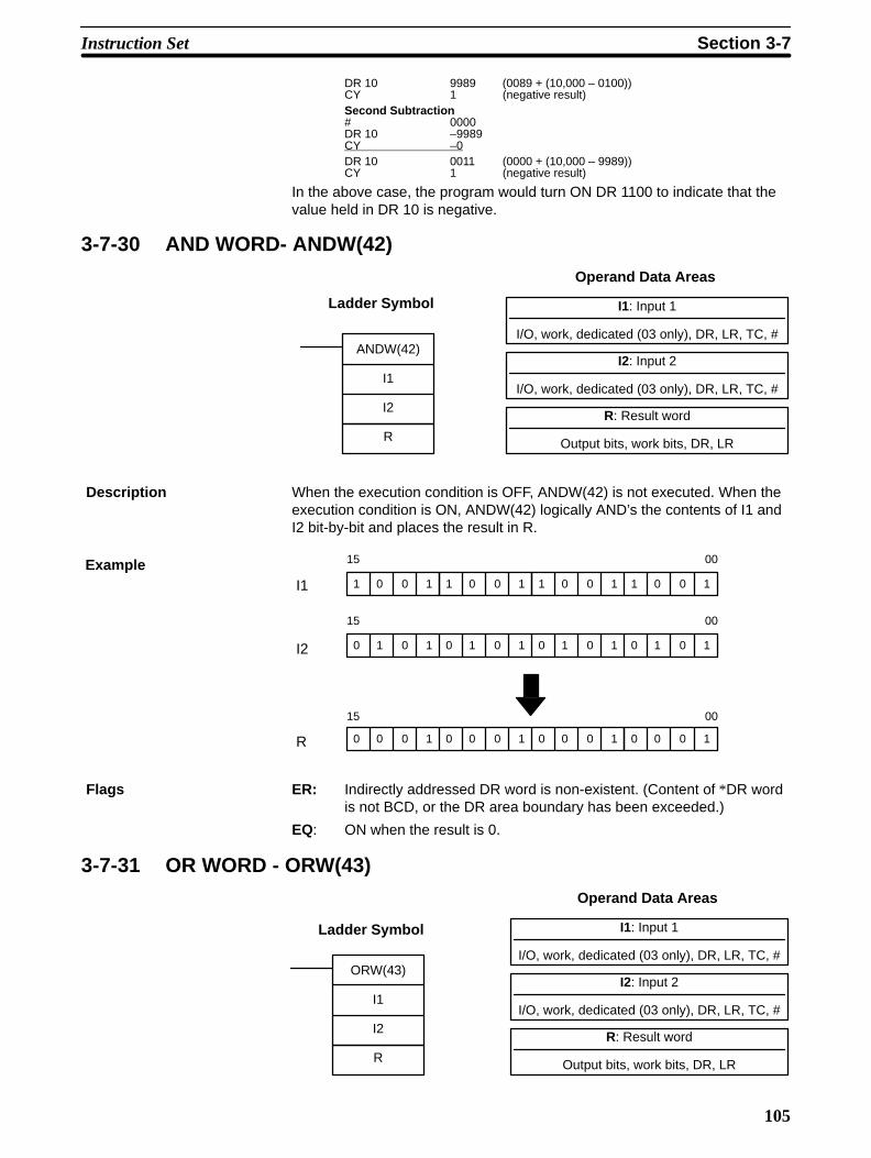
105
DR 10 9989 (0089 + (10,000 – 0100))CY 1 (negative result)Second Subtraction# 0000DR 10 –9989CY –0DR 10 0011 (0000 + (10,000 – 9989))CY 1 (negative result)
In the above case, the program would turn ON DR 1100 to indicate that thevalue held in DR 10 is negative.
3-7-30 AND WORD- ANDW(42)
I1: Input 1
I/O, work, dedicated (03 only), DR, LR, TC, #
I2: Input 2
I/O, work, dedicated (03 only), DR, LR, TC, #
Ladder Symbol
Operand Data Areas
R: Result word
Output bits, work bits, DR, LR
ANDW(42)
I1
I2
R
When the execution condition is OFF, ANDW(42) is not executed. When theexecution condition is ON, ANDW(42) logically AND’s the contents of I1 andI2 bit-by-bit and places the result in R.
1 0 0 1 1 0 0 1 1 0 0 1 1 0 0 1
15 00
0 1 0 1 0 1 0 1 0 1 0 1 0 1 0 1
0 0 0 1 0 0 0 1 0 0 0 1 0 0 0 1
15 00
15 00
I1
I2
R
Example
ER: Indirectly addressed DR word is non-existent. (Content of *DR wordis not BCD, or the DR area boundary has been exceeded.)
EQ: ON when the result is 0.
3-7-31 OR WORD - ORW(43)
I1: Input 1
I/O, work, dedicated (03 only), DR, LR, TC, #
I2: Input 2
I/O, work, dedicated (03 only), DR, LR, TC, #
Ladder Symbol
Operand Data Areas
R: Result word
Output bits, work bits, DR, LR
ORW(43)
I1
I2
R
Description
Flags
Instruction Set Section 3-7
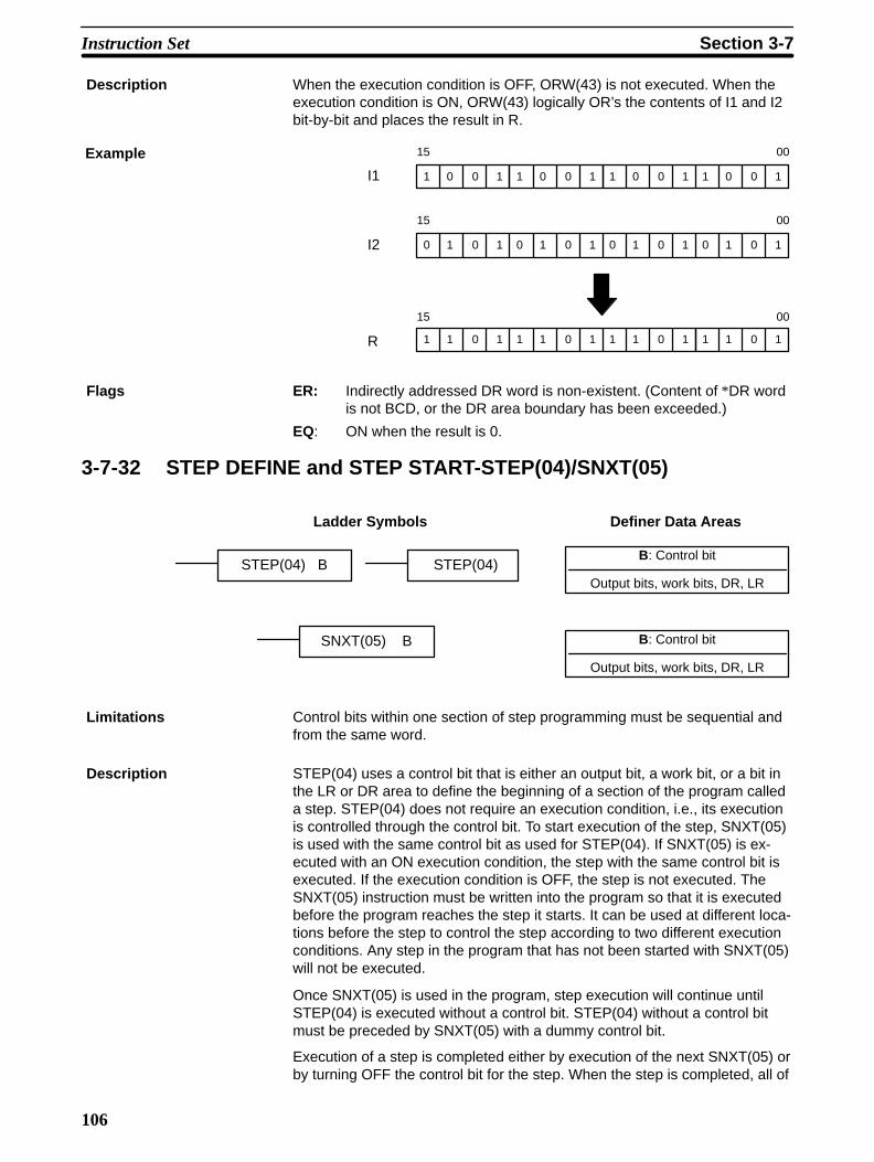
106
When the execution condition is OFF, ORW(43) is not executed. When theexecution condition is ON, ORW(43) logically OR’s the contents of I1 and I2bit-by-bit and places the result in R.
1 0 0 1 1 0 0 1 1 0 0 1 1 0 0 1
15 00
0 1 0 1 0 1 0 1 0 1 0 1 0 1 0 1
1 1 0 1 1 1 0 1 1 1 0 1 1 1 0 1
15 00
15 00
I1
I2
R
Example
ER: Indirectly addressed DR word is non-existent. (Content of *DR wordis not BCD, or the DR area boundary has been exceeded.)
EQ: ON when the result is 0.
3-7-32 STEP DEFINE and STEP START-STEP(04)/SNXT(05)
B: Control bit
Output bits, work bits, DR, LR
Ladder Symbols Definer Data Areas
STEP(04) B STEP(04)
B: Control bit
Output bits, work bits, DR, LR
SNXT(05) B
Control bits within one section of step programming must be sequential andfrom the same word.
STEP(04) uses a control bit that is either an output bit, a work bit, or a bit inthe LR or DR area to define the beginning of a section of the program calleda step. STEP(04) does not require an execution condition, i.e., its executionis controlled through the control bit. To start execution of the step, SNXT(05)is used with the same control bit as used for STEP(04). If SNXT(05) is ex-ecuted with an ON execution condition, the step with the same control bit isexecuted. If the execution condition is OFF, the step is not executed. TheSNXT(05) instruction must be written into the program so that it is executedbefore the program reaches the step it starts. It can be used at different loca-tions before the step to control the step according to two different executionconditions. Any step in the program that has not been started with SNXT(05)will not be executed.
Once SNXT(05) is used in the program, step execution will continue untilSTEP(04) is executed without a control bit. STEP(04) without a control bitmust be preceded by SNXT(05) with a dummy control bit.
Execution of a step is completed either by execution of the next SNXT(05) orby turning OFF the control bit for the step. When the step is completed, all of
Description
Flags
Limitations
Description
Instruction Set Section 3-7

107
operand bits in the step are turned OFF and all timers in the step are reset totheir SVs. Counters, shift registers, and bits used in KEEP(12) maintain sta-tus. Two simple steps are shown below.
SNXT(05) 0200
STEP(04) 0200
0000
Step controlled by 0200
SNXT(05) 0201
STEP(04) 0201
0001
Step controlled by 0201
SNXT(05) 0202
STEP(04)
0002
Starts step execution
Ends step execution
1st step
2nd step
Address Instruction Operands Address Instruction Operands
000 LD 0000
001 SNXT(05) 0200
002 STEP(04) 0200
Step controlled by 0200.
030 LD 0001
031 SNXT(05) 0201
032 STEP(04) 0201
Step controlled by 0201.
051 LD 0002
052 SNXT(05) 0202
053 STEP(04) ---
Steps can be programmed in consecutively. Each step must start withSTEP(04) and generally ends with SNXT(05). When steps are programmedin series, three types of execution are possible: sequential, branching, or par-allel. The execution conditions for, and the positioning of, SNXT(05) deter-mine how the steps are executed.
Interlocks and END(01) cannot be used within step programs.
Bits used as control bits must not be used anywhere else in the program un-less they are being used to control the operation of the step.
If output bits, work bits, or LR bits are used for control bits, their status will belost during any power interruption. If it is necessary to maintain status to re-sume execution at the same step, DR bits must be used.
0411: Step Start Flag; turns ON for one scan when STEP(04) is executedand can be used to reset counters in steps as shown below if neces-sary.
Precautions
Flags
Instruction Set Section 3-7
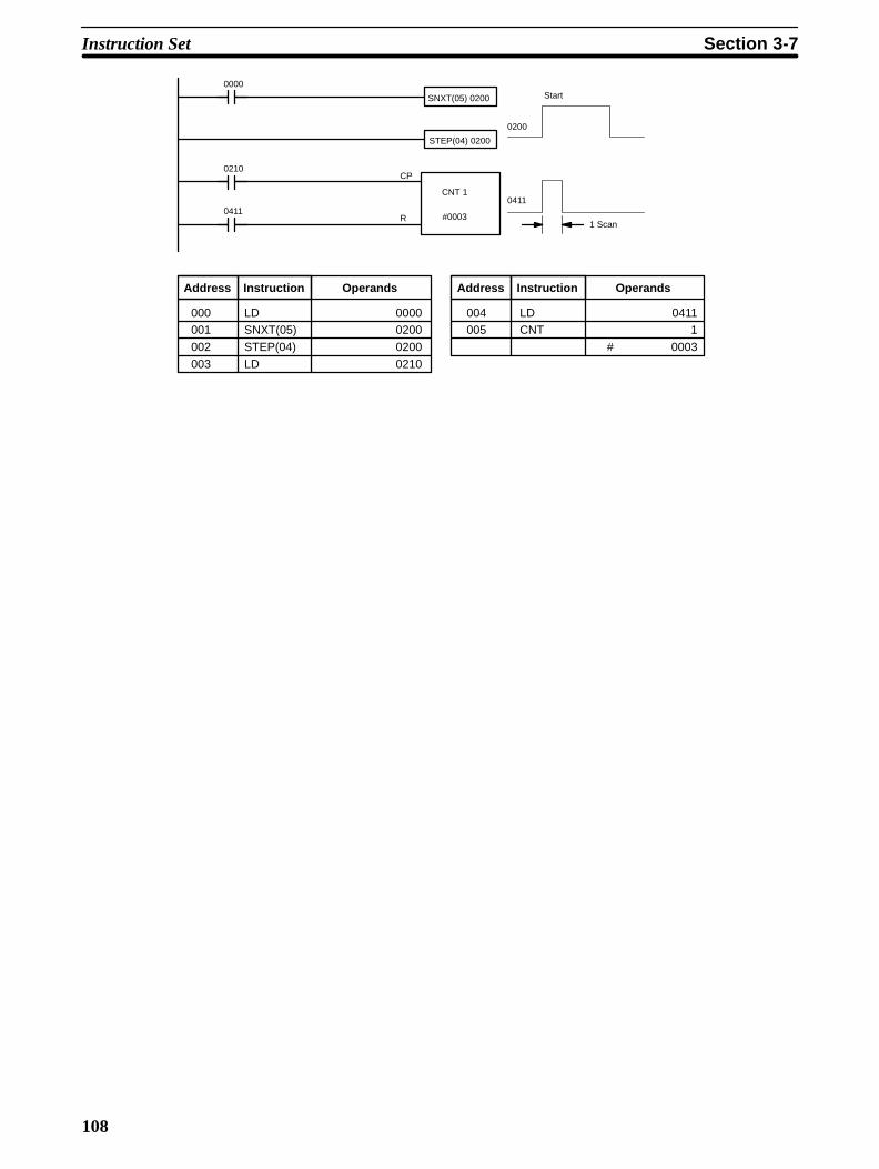
108
SNXT(05) 0200
CP
R
CNT 1
#0003
0000
0210
0411
STEP(04) 0200
1 Scan
0411
0200
Start
Address Instruction Operands Address Instruction Operands
000 LD 0000
001 SNXT(05) 0200
002 STEP(04) 0200
003 LD 0210
004 LD 0411
005 CNT 1
# 0003
Instruction Set Section 3-7

109
3-8 DebuggingAfter inputting a program and correcting it for syntax errors, it must be ex-ecuted and all execution errors must be eliminated. Execution errors includean excessively long scan and inappropriate control actions, i.e., the programnot doing what it is designed to do.
If desired, the program can first be executed isolated from the actual controlsystem and wired to dummy inputs and outputs to check for certain types oferrors before actual trial operation with the controlled system.
3-8-1 Displaying and Clearing Error MessagesWhen an error occurs during program execution, it can be displayed for iden-tification by pressing CLR, FUN, 6, 1 and then MON. If an error message isdisplayed, MON can be pressed to access any other error messages that arestored by the system in memory. If MON is pressed in PRGM mode, the errormessage will be cleared from memory; be sure to write down the error mes-sage when required before pressing MON. CHECK OK will be displayedwhen the last message has been cleared.
In RUN mode errors cannot be cleared by pressing MON. Also, if the causeof the error still exists, it must be eliminated before the error message can becleared. Refer to Section 5 Troubleshooting for all details on all error mes-sages. The sequence in which error messages are displayed depends on thepriority of the errors.
Although error messages can be displayed in any mode, they can be clearedonly in PROGRAM mode. There is no way to restart the PC following a fatalerror without first clearing the error message in PROGRAM mode.
Key Sequence
The following displays show some of the messages that may appear. Referto Section 5 Troubleshooting for an extensive list of error messages, theirmeanings, and the appropriate responses.
Fatal errors
All errorshave been cleared
0-000
0 ERROR MESSAGE
0 ERROR MESSAGE CHECK OK
0 ERROR MESSAGE MEMORY ERR
0 ERROR MESSAGE NO END INST
0 ERROR MESSAGE CHECK OK
Example
Debugging Section 3-8
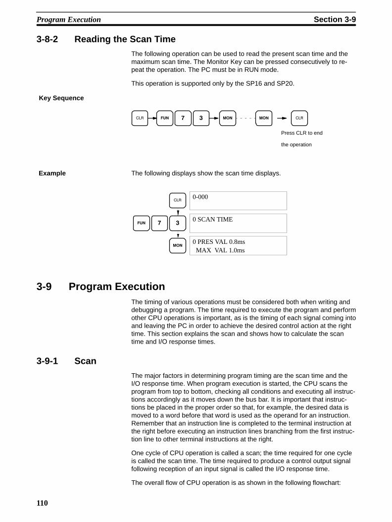
110
3-8-2 Reading the Scan Time
The following operation can be used to read the present scan time and themaximum scan time. The Monitor Key can be pressed consecutively to re-peat the operation. The PC must be in RUN mode.
This operation is supported only by the SP16 and SP20.
Key Sequence
Press CLR to end
the operation
The following displays show the scan time displays.
0-000
0 SCAN TIME
0 PRES VAL 0.8ms MAX VAL 1.0ms
3-9 Program ExecutionThe timing of various operations must be considered both when writing anddebugging a program. The time required to execute the program and performother CPU operations is important, as is the timing of each signal coming intoand leaving the PC in order to achieve the desired control action at the righttime. This section explains the scan and shows how to calculate the scantime and I/O response times.
3-9-1 Scan
The major factors in determining program timing are the scan time and theI/O response time. When program execution is started, the CPU scans theprogram from top to bottom, checking all conditions and executing all instruc-tions accordingly as it moves down the bus bar. It is important that instruc-tions be placed in the proper order so that, for example, the desired data ismoved to a word before that word is used as the operand for an instruction.Remember that an instruction line is completed to the terminal instruction atthe right before executing an instruction lines branching from the first instruc-tion line to other terminal instructions at the right.
One cycle of CPU operation is called a scan; the time required for one cycleis called the scan time. The time required to produce a control output signalfollowing reception of an input signal is called the I/O response time.
The overall flow of CPU operation is as shown in the following flowchart:
Example
Program Execution Section 3-9

111
Power application
Initialization on power-up
Overseeing processes
Program execution
I/O refresh
Service ProgrammingConsole commands
Service PC Link
• Transfer the program from EEPROM to RAM.
• Resets the watchdog timer.
• Using the programmed code, executes eachinstruction from address 000 through to theEND instruction
• Output RefreshRefreshes output bits according to output bitstatus (results of the executed program).
• Services the Programming Console (monitor,edits, etc.).
• Data communication with other PCsvia the Link Adapter.
• Resets data areas (except DR area), resets alltimers, and checks the link status.
• Checks the RUN status and Program Memory.
• Input RefreshRefreshes input bits according to input signals.
PC scan timeThe time required toperform this process.
A
B
C
D
E
• After power application, there is a 2.5-s delaybefore the start of initialization.
The first initialization process is performed only once, immediately after pow-er is applied to the PC. The remaining operations are performed in cyclicfashion, with each cycle forming one scan. The scan time is the time that isrequired for the CPU to complete one of these cycles. This cycle includesbasically five types of operation.
OverseeingProgram executionI/O refreshProgramming Console servicingPC Link servicing
The scan time is the total time required for the PC to perform all of the aboveoperations. The present and maximum scan time can be read out from theProgramming Console with the SP16 or SP20. Refer to 3-8-2 Reading theScan Time for details.
All peripheral devices are serviced once each scan in the order given above.
Within the PC, the watchdog timer measures the scan time and compares itto a set value. If the scan time exceeds the set value of the watchdog timer,100 ms, a CPU error is generated and the CPU stops. One scan time is ap-proximately 300 µs plus the time required for program execution.
3-10 I/O Response TimeThe I/O response time is the time it takes for the PC to output a control signalafter it has received an input signal. The time it takes to respond depends onthe scan time and when the CPU receives the input signal relative to the I/Orefresh period.
Watchdog Timer and LongScan Times
I/O Response Time Section 3-10
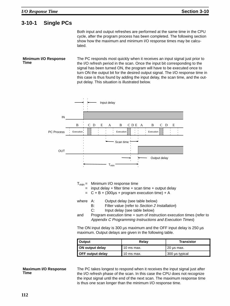
112
3-10-1 Single PCs
Both input and output refreshes are performed at the same time in the CPUcycle, after the program process has been completed. The following sectionshow how the maximum and minimum I/O response times may be calcu-lated.
The PC responds most quickly when it receives an input signal just prior tothe I/O refresh period in the scan. Once the input bit corresponding to thesignal has been turned ON, the program will have to be executed once toturn ON the output bit for the desired output signal. The I/O response time inthis case is thus found by adding the input delay, the scan time, and the out-put delay. This situation is illustrated below.
Input delay
IN
OUT
PC Process Execution Execution Execution
Scan time
Output delay
Tmin
AB C D E AB C D E B D EC
Tmin = Minimum I/O response time= input delay + filter time + scan time + output delay= C + B + (300µs + program execution time) + A
where A: Output delay (see table below)B: Filter value (refer to Section 2 Installation)C: Input delay (see table below)
and Program execution time = sum of instruction execution times (refer toAppendix C Programming Instructions and Execution Times)
The ON input delay is 300 µs maximum and the OFF input delay is 250 µsmaximum. Output delays are given in the following table.
Output Relay Transistor
ON output delay 10 ms max. 20 µs max.
OFF output delay 10 ms max. 300 µs typical
The PC takes longest to respond when it receives the input signal just afterthe I/O refresh phase of the scan. In this case the CPU does not recognizethe input signal until the end of the next scan. The maximum response timeis thus one scan longer than the minimum I/O response time.
Minimum I/O ResponseTime
Maximum I/O ResponseTime
I/O Response Time Section 3-10

113
Execu-tion
input delay
IN
OUT
PC Process
Scan time outputdelay
Tmax
AC D E AB C D E B DC
Tmax = Maximum I/O response time= input delay + filter time + (scan time x 2) + output delay= C + (B + 0.5 ms) + ((300 µs + program execution time) x 2) + A
3-10-2 Multiple PCsIf more than one PC is linked via a Link Adapter in a distributed control sys-tem, the I/O response time is increased with every PC having their own re-sponse time. The average I/O response time given as a function of the num-ber of linked PCs is shown in the following graph. For a system of four PCs,the maximum I/O response time is 0.4 s.
0.4
0.3
0.2
0.1
1 2 3 4
Average I/O response time(s) 128 pts.
64 pts.
No. of linked PCs
Note The duration required to process linked PCs is increased if a PC alreadylinked is disconnected from the network.
I/O Response Time Section 3-10
115
SECTION 4Operation
This section describes how to monitor and maintain PC operation once a program has been input and transferred. It alsoprovides the procedure for initializing memory cards. Refer to 3-5-8 Program Transfer for the procedures for transferringprograms and data between the Programming Console and the PC or Memory Cards.
4-1 Monitoring Operation and Modifying Data 116 . . . . . . . . . . . . . . . . . . . . . . . . . . . . . . 4-1-1 Bit/Multibit Monitor 116 . . . . . . . . . . . . . . . . . . . . . . . . . . . . . . . . . . . . . . . 4-1-2 Force Set/Reset 119 . . . . . . . . . . . . . . . . . . . . . . . . . . . . . . . . . . . . . . . . . . . 4-1-3 Hexadecimal/BCD Data Modification 120 . . . . . . . . . . . . . . . . . . . . . . . . . 4-1-4 Binary Monitor 121 . . . . . . . . . . . . . . . . . . . . . . . . . . . . . . . . . . . . . . . . . . . 4-1-5 Binary Data Modification 122 . . . . . . . . . . . . . . . . . . . . . . . . . . . . . . . . . . .
4-2 Memory Card Initialization 123 . . . . . . . . . . . . . . . . . . . . . . . . . . . . . . . . . . . . . . . . . .
116
4-1 Monitoring Operation and Modifying Data
The simplest form of operation monitoring is to display the address whoseoperand bit status is to be monitored using the Program Read or the searchoperation. As long as the operation is performed in RUN mode, the status ofany bit displayed will be indicated.
This section provides other procedures for monitoring data as well as proce-dures for modifying data that already exists in a data area. Data that can bemodified includes the PV (present value) for any timer or counter.
All monitor operations in this section can be performed in RUN or PRO-GRAM mode and can be cancelled by pressing CLR.
All data modification operations are performed after first performing one ofthe monitor operations. Data modification is possible in either PROGRAM orRUN mode.
4-1-1 Bit/Multibit Monitor
The status of any bit or word in any data area can be monitored using thefollowing operation. Although the operation is possible in any mode, ON/OFFstatus displays will be provided for bits in RUN mode only.
The Bit/Multibit Monitor operation can be entered either from a cleared dis-play by designating the first bit or word to be monitored or it can be enteredfrom any address in the program by displaying the bit or word address whosestatus is to be monitored and pressing MON.
When a bit is monitored, it’s ON/OFF status will be displayed (in RUN mode);when a word address is designated other than a timer or counter, the digitcontents of the word will be displayed; and when a timer or counter numberis designated, the PV of the timer will be displayed and a small box will ap-pear if the completion flag of a timer or counter is ON. When multiple wordsare monitored, a space will appear between the different address designa-tions. The status of the arithmetic flags are cleared when END(01) is ex-ecuted and cannot be monitored.
Up to three memory addresses, either bits, words, or a combination of both,can be monitored at once. To continue designating addresses with the sec-ond of the following key sequences.
During a monitor operation the up and down keys can be pressed to incre-ment and decrement the leftmost address on the display and CLR can bepressed to cancel monitoring the leftmost address on the display. If the lastaddress is cancelled, the monitor operation will be cancelled. The monitoroperation can also be cancelled regardless of the number of addresses beingmonitored by pressing SHIFT and then CLR.
LD and OUT can be used only to designate the first address to be displayed;they cannot be used when an address is already being monitored.
Monitoring Operation and Modifying Data Section 4-1

117
Bit/Word MonitorKey Sequence
[Bit address]
Cancels monitoroperation
Clears leftmost address
Shifts to wordmonitor
Program Read
Multibit/Word MonitorKey Sequence
[Bit Address]
Cancels one bit
Scrolls the dis-play
Cancels allmonitoring
Monitoring Operation and Modifying Data Section 4-1

118
The following examples show various applications of this monitor operation.
Program Read then Monitor
Indicates Completion flag is ON
Monitor operationis cancelled
0-001
0-001READTIM 00
0 T 00 1234
0 T 01!0000
0-001TIM 01
Bit Monitor
0-000
0-000READ ONLD 0000
0-001READ OFFAND 0001
Word Monitor
0-000
0-000 CHANNEL 00
0 cD10 0000
0 cD09 FFFF
0-000 CHANNEL DR 10
Examples
Monitoring Operation and Modifying Data Section 4-1

119
Multi-address Monitoring
0-000
0-000TIM 00
0 T 00 0100
0 0000 T 00 0100
0 0001 T 00 0100
0 0001 T 00 ^OFF 0100
0 cD00 0001 T 00 10FF ^OFF 0100
0 cD00 0001 T 00 10FF ^OFF 0100
0 T 00 cD00 0001 0100 10FF OFF
0 cD00 0001 10FF ^OFF
0 0001 ^OFF
0-000CONT 0001
Cancels monitoring of leftmost address
Cancels Monitor operation
or
4-1-2 Force Set/ResetWhen the Bit/Multibit Monitor operation is being performed and a bit, timer, orcounter address is leftmost on the display, CHG and ENT can be pressed toturn ON/OFF the bit, start/reset the timer, or increment/reset the counter.Timers will not operate in PROGRAM mode. Dedicated flags and bits cannotbe turned ON and OFF with this operation.
Bit status will remain ON or OFF until the I/O bit status is refreshed, whichoccurs each scan. Hence, forced status will be canceled at each I/O refresh.If a timer is started, the Completion Flag for it will be turned ON when SV hasbeen reached.
This operation can be used in RUN mode to check wiring of outputs from thePC prior to actual program execution.
Key Sequence
Bit/word Monitor
Mutlibit/word Monitor
Monitoring Operation and Modifying Data Section 4-1
120
The following example shows how either bits or counters can be controlledwith the Force Set/Reset operation. The displays shown below are for thefollowing program section.
000 LD 0000
001 LD 0200
002 CNT 05
# 0100
003 LD CNT 05
004 OUT 0101
0000
CNT05
0101
0200
CP
R
CNT 05
#0100
Address Instruction Operands
The following displays show what happens when CNT 05 is set whenbit 0000 is ON.
(This example is in RUN mode.)
Indicates that force set/reset is in progress.
0-000
0-000CNT 00
0-000CNT 05
0 C 05 0100
0 0000 C 05 0100
0 0000 C 05 ^OFF 0100
0 0000 C 05~ OFF 0100
0 0000 C 05 ^ ON 0099
0 0000 C 05 ^OFF 0099
After one scan the valueof 0000 is reset to 0.
4-1-3 Hexadecimal/BCD Data ModificationWhen the Bit/Multibit Monitor operation is being performed and a BCD orhexadecimal value is leftmost on the display, CHG can be input to changethe value. Dedicated words cannot be changed.
If a timer or counter is leftmost on the display, the PV will be displayed andwill be the value changed. PV can be changed in RUN mode only when thetimer or counter is operating.
To change contents of the leftmost word address, press CHG, input the de-sired value, and press ENT.
Example
Monitoring Operation and Modifying Data Section 4-1
121
Key Sequence
Word currentlymonitored onleft of display.
[ Data ]
The following example shows the effects of changing the PV of a timer.
This example is in RUN mode
Timing
Timing
PV changed
Timing
Timing
0-000
0-000TIM 00
0 T 00 0122
0 PRES VAL? T 00 0119 ????
0 PRES VAL? T 00 0100 0200
0 T 00 0199
4-1-4 Binary Monitor
You can specify that the contents of a monitored word be displayed in binaryby pressing SHIFT and MON after the word address has been input. Wordscan be successively monitored by using the up and down keys to incrementand decrement the displayed word address. To clear the binary display, pressCLR.
Example
Monitoring Operation and Modifying Data Section 4-1
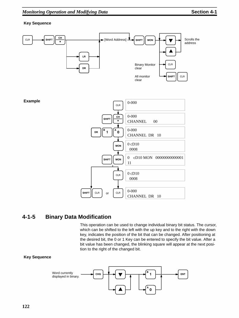
122
Key Sequence
[Word Address]
Binary Monitorclear
All monitorclear
Scrolls theaddress
0-000
0-000CHANNEL 00
0 cD10 0008
0 cD10 MON 0000000000000111
0-000CHANNEL DR 10
0 cD10 0008
0-000CHANNEL DR 10
or
4-1-5 Binary Data ModificationThis operation can be used to change individual binary bit status. The cursor,which can be shifted to the left with the up key and to the right with the downkey, indicates the position of the bit that can be changed. After positioning atthe desired bit, the 0 or 1 Key can be entered to specify the bit value. After abit value has been changed, the blinking square will appear at the next posi-tion to the right of the changed bit.
Key Sequence
Word currently displayed in binary.
Example
Monitoring Operation and Modifying Data Section 4-1
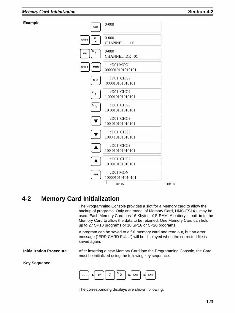
123
Bit 15 Bit 00
0-000
0-000CHANNEL 00
0-000CHANNEL DR 01
cD01 MON0000010101010101
cD01 CHG? 000010101010101
cD01 CHG?1 00010101010101
cD01 CHG?10 0010101010101
cD01 CHG?100 010101010101
cD01 CHG?1000 10101010101
cD01 CHG?100 010101010101
cD01 CHG?10 0010101010101
cD01 MON1000010101010101
4-2 Memory Card InitializationThe Programming Console provides a slot for a Memory card to allow thebackup of programs. Only one model of Memory Card, HMC-ES141, may beused. Each Memory Card has 16 Kbytes of S-RAM. A battery is built-in to theMemory Card to allow the data to be retained. One Memory Card can holdup to 27 SP10 programs or 18 SP16 or SP20 programs.
A program can be saved to a full memory card and read out, but an errormessage (“ERR CARD FULL”) will be displayed when the corrected file issaved again.
After inserting a new Memory Card into the Programming Console, the Cardmust be initialized using the following key sequence.
Key Sequence
The corresponding displays are shown following.
Example
Initialization Procedure
Memory Card Initialization Section 4-2
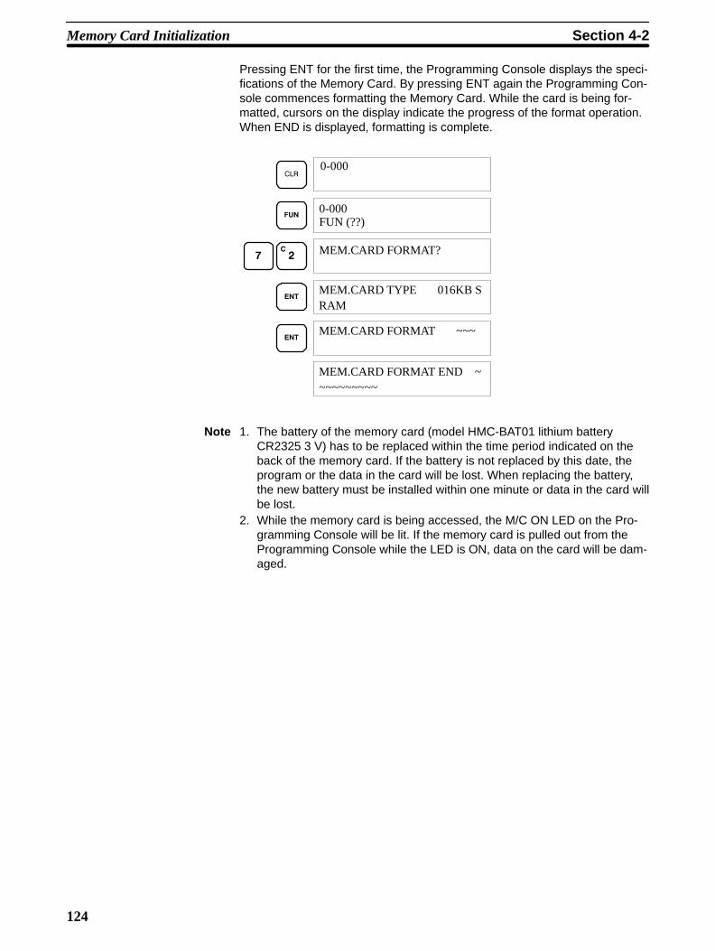
124
Pressing ENT for the first time, the Programming Console displays the speci-fications of the Memory Card. By pressing ENT again the Programming Con-sole commences formatting the Memory Card. While the card is being for-matted, cursors on the display indicate the progress of the format operation.When END is displayed, formatting is complete.
MEM.CARD TYPE 016KB SRAM
MEM.CARD FORMAT?
0-000
0-000FUN (??)
MEM.CARD FORMAT ~~~
MEM.CARD FORMAT END ~~~~~~~~~~
Note 1. The battery of the memory card (model HMC-BAT01 lithium batteryCR2325 3 V) has to be replaced within the time period indicated on theback of the memory card. If the battery is not replaced by this date, theprogram or the data in the card will be lost. When replacing the battery,the new battery must be installed within one minute or data in the card willbe lost.
2. While the memory card is being accessed, the M/C ON LED on the Pro-gramming Console will be lit. If the memory card is pulled out from theProgramming Console while the LED is ON, data on the card will be dam-aged.
Memory Card Initialization Section 4-2

125
A number of errors relating to the Memory Card may occur during the pro-gram check. If one of the following errors is shown on the display, programtransfer cannot proceed.
Error Message Meaning/Correction
NO END INST END instruction cannot be found. Include an END instructionat the end of the program.
(Program address)or????
Displayed address has the inappropriate operand orinappropriate instruction. Correct the program and transferit to the PC again.
ERR CARD ~ ProCo The program stored in the memory card contains errors.The memory card data is transferred to theProgramming Console’s RAM to allow it to be checked.Perform a program check to confirm the program.
NO SUPPORTCARD
The Memory Card is not initialized, or is not supported by theProgramming Console (SP10-PRO01-V1).Initialize the Memory Card (or check the specification of thememory card).
ERR CARD FULL The memory card is full. Delete unneeded files or use anotherinitialized Memory Card.
PTCT ON OREPROM
The Memory Card protect switch is ON, or the insertedmemory card is an EPROM memory card. Adjust the protectswitch, or use a RAM Memory Card.
NO MEM. CARD Memory Card is not inserted properly in the card slot.
Error Messages
Memory Card Initialization Section 4-2

127
SECTION 5Troubleshooting
5-1 Alarm Indicators 128 . . . . . . . . . . . . . . . . . . . . . . . . . . . . . . . . . . . . . . . . . . . . . . . . . . . 5-2 Reading and Clearing Errors and Messages 128 . . . . . . . . . . . . . . . . . . . . . . . . . . . . . . 5-3 Error Messages 128 . . . . . . . . . . . . . . . . . . . . . . . . . . . . . . . . . . . . . . . . . . . . . . . . . . . . 5-4 Error Flags 129 . . . . . . . . . . . . . . . . . . . . . . . . . . . . . . . . . . . . . . . . . . . . . . . . . . . . . . .
!
128
5-1 Alarm IndicatorsThere are three indicators on the front of the CPU that provide visual indica-tion of errors in the PC. The power indicator (POWER) indicates errors dueto incorrect application of power to the PC; the error indicator (ERROR) indi-cates fatal errors (i.e., ones that will stop PC operation); the link indicator(LINK) indicates PC link errors.
WARNING The PC will turn ON the error indicator (ERROR), stop program execution, andturn OFF all outputs from the PC for most hardware errors and for fatal softwareerrors. PC operation will continue for all other errors. It is the user’s responsibilityto take adequate measures to ensure that a hazardous situation will not resultfrom automatic system shutdown for fatal errors and to ensure that properactions are taken for errors for which the system is not automatically shut down.System flags can be used to program proper actions.
5-2 Reading and Clearing Errors and MessagesSystem error messages can be displayed on the Programming Console.
On the Programming Console, press the CLR, FUN, 6, 1, and MON keys. Ifthere are multiple error messages stored by the system, the MON key can bepressed again to access the next message. If the system is in PROGRAMmode, pressing the MON key will clear the error message, so be sure to writedown all message errors as you read them.
It is not possible to clear an error or a message while in RUN mode; the PCmust be in PROGRAM mode.
When all messages have been cleared, “CHECK OK” will be displayed andthe ERROR LED will turn OFF.
If a “COMM ERR” occurs, the Programming Console will ignore any key op-eration other than CLR, so press CLR to clear the communication error andallow access via the PC Link to CPU Unit #0. Ensure the correct connectionof cables between the Units.
Note If a memory error occurs in the PC, the Programming Console may not func-tion properly if the program is transferred from the PC to the ProgrammingConsole. Perform a program comparison between the transferred programand the program in the PC to see if the programs are the same.
5-3 Error MessagesThere are basically two types of errors for which messages are displayed:programming errors and fatal operating errors.
The type of error can be quickly determined from the indicators on the CPU,as described below for the two types of errors. If the status of an indicator isnot mentioned in the description, it makes no difference whether it is lit or not.
After eliminating the cause of an error, clear the error message from memorybefore resuming operation.
The following error messages appear if an error occurs during programming.The Programming Console will be in PROGRAM mode. The POWER indica-tor will be lit and the RUN indicator will not be lit for either of these.
Programming Errors
Error Messages Section 5-3

129
The following error messages may appear when inputting a program. Correctthe error as indicated and continue with the input operation.
Error Message Error Type Possible Cause/Correction
PRGM OVER Program toolarge
Program size exceeds the capacity. (The lastaddress is not a NOP instruction, so theprogram cannot be written.)Clear any data after the END instruction orshorten the program.
ADR OVER Address toolarge
Program exceeds program memory’s lastaddress.Set the address again.
I/O No. ERR Operand error An illegal value has been entered for anoperand. Reconfirm the allowable operandarea for each instruction, and correct thedata.
The following error messages appear for errors that occur after program ex-ecution has been started. PC operation and program execution will halt whenany of the following errors occur. The status of the indicators is given foreach error.
Error Type Error Message LED Indicator Possible Cause/Correction
POWER RUN ERROR
Power failure - Check the power supply, voltage, and wiring.
CPU error - The watchdog timer (100 ms) has timed out.Turn power OFF, change to PROGRAM mode,and turn power ON again.
Memory error MEMORY ERR The program may contain an error. Correct theprogram, then transfer the corrected program tothe PC from the Programming Console.Alternatively, turn the PC power OFF and ON. Ifthe memory error occurs when power is switchedON, an error may have occurred when theprogram was transferred from EEPROM to RAM.
No ENDinstruction
NO END INST The END instruction cannot be found in theprogram.Change to PROGRAM mode, and add an ENDinstruction to the end of the program.
Lit Not lit
Note When a communication error occurs during a PC Link operation, the LINKLED will go OFF.
A number of other error messages are detailed within this manual. Errors inprogram input can be found in 3-5 Inputting the Program and errors in pro-gram transfer are detailed in 3-5-8 Program Transfers.
5-4 Error Flags
A number of flags are available in the dedicated bit area that can be used fortroubleshooting. Details are provided in 3-2-5 Dedicated Bits.
Error Messages
Operating Errors
Other Error Messages
Error Flags Section 5-4

131
Appendix AStandard Models
Name Specifications Model number
SP10 PC 6 inputs (DC; one common) 100 to 240 VAC Relay outputs SP10-DR-A
4 outputs Transistor outputs SP10-DT-A
(2 commons, 2 pts each) 24 VDC Relay outputs SP10-DR-D
Transistor outputs SP10-DT-D
SP16 PC 10 inputs 100 to 240 VAC Relay outputs SP16-DR-A
(DC; one common, 2 pts; Transistor outputs SP16-DT-A
one common, 8 pts) 24 VDC Relay outputs SP16-DR-D
6 outputs (3 commons, 2 pts each)
Transistor outputs SP16-DT-D
SP20 PC 12 inputs 100 to 240 VAC Relay outputs SP20-DR-A
(DC; 2 commons, 2 pts each; Transistor outputs SP20-DT-A
one common, 8 pts) 24 VDC Relay outputs SP20-DR-D
8 outputs (4 commons, 2 pts each)
Transistor outputs SP20-DT-D
ProgrammingConsole
Vertical, hand-held with backlit LCD display. Compatible with Memory Cards.Memory Card and Connecting Cable sold separately (see below). Usable onlywith SP-series PCs.
SP10-PRO01-V1
ProgrammingConsole Connecting Cable
Connect Programming Console to CPU or toLink Adapter. Same as 2-m and 4-m LinkAdapter Connecting Cables.*
2-m cable SP10-CN221
4-m cable SP10-CN421
Link Adapter
Used to link up to 4 SP-series CPUs. Cables sold separately (see below). SP10-AL001
Link AdapterConnecting Cable
Connect the CPUs and Link Adapter.* 20-cmcable
Do not connectto Programming
SP10-CN211
1-mcable
Console. SP10-CN121
2-m cable SP10-CN221
4-m cable SP10-CN421
Memory Card 16-Kbyte SRAM cards (battery built in). Battery will last 5 years from when it ismounted to the Memory Card.
HMC-ES141
MountingAccessories
50-cm DIN Track7.3 mmDepth
PFP-50N
1-m DIN Track PFP-100N
1-m DIN Track 16.0 mmDepth PFP-100N2
End Plate PFP-M
Spacer PFP-S

Standard Models Appendix A
132
Name Model numberSpecifications
SimulationSwitchboard
Board with 6 switches and AC power cord (power switch also included) SP10-ETL01SP16-ETL01SP20-ETL01
*Note: The cables between CPUs and the Link Adapter must be 4 m or less. The sum of the distance be-tween CPU #0 and the Link Adapter and the distance between the Link Adapter and the Program-ming Console must be 4.2 m or less.
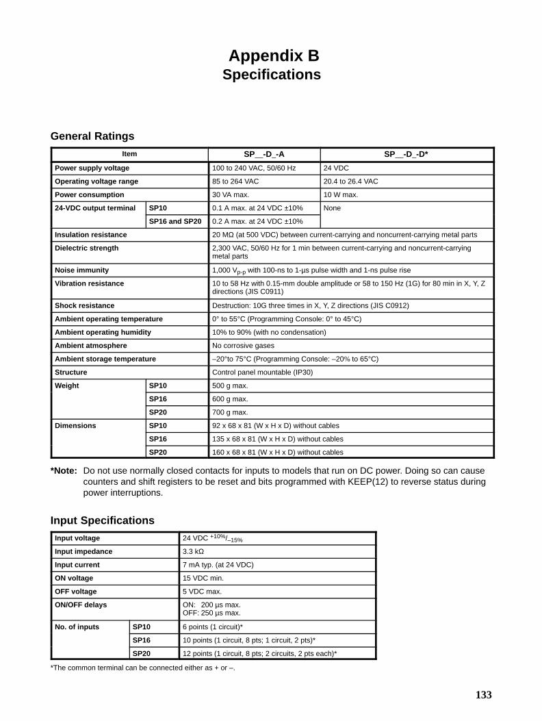
133
Appendix BSpecifications
General Ratings
Item SP__-D_-A SP__-D_-D*
Power supply voltage 100 to 240 VAC, 50/60 Hz 24 VDC
Operating voltage range 85 to 264 VAC 20.4 to 26.4 VAC
Power consumption 30 VA max. 10 W max.
24-VDC output terminal SP10 0.1 A max. at 24 VDC ±10% None
SP16 and SP20 0.2 A max. at 24 VDC ±10%
Insulation resistance 20 MΩ (at 500 VDC) between current-carrying and noncurrent-carrying metal parts
Dielectric strength 2,300 VAC, 50/60 Hz for 1 min between current-carrying and noncurrent-carryingmetal parts
Noise immunity 1,000 Vp-p with 100-ns to 1-µs pulse width and 1-ns pulse rise
Vibration resistance 10 to 58 Hz with 0.15-mm double amplitude or 58 to 150 Hz (1G) for 80 min in X, Y, Zdirections (JIS C0911)
Shock resistance Destruction: 10G three times in X, Y, Z directions (JIS C0912)
Ambient operating temperature 0° to 55°C (Programming Console: 0° to 45°C)
Ambient operating humidity 10% to 90% (with no condensation)
Ambient atmosphere No corrosive gases
Ambient storage temperature –20°to 75°C (Programming Console: –20% to 65°C)
Structure Control panel mountable (IP30)
Weight SP10 500 g max.
SP16 600 g max.
SP20 700 g max.
Dimensions SP10 92 x 68 x 81 (W x H x D) without cables
SP16 135 x 68 x 81 (W x H x D) without cables
SP20 160 x 68 x 81 (W x H x D) without cables
*Note: Do not use normally closed contacts for inputs to models that run on DC power. Doing so can causecounters and shift registers to be reset and bits programmed with KEEP(12) to reverse status duringpower interruptions.
Input Specifications
Input voltage 24 VDC +10%/–15%
Input impedance 3.3 kΩ
Input current 7 mA typ. (at 24 VDC)
ON voltage 15 VDC min.
OFF voltage 5 VDC max.
ON/OFF delays ON: 200 µs max.OFF: 250 µs max.
No. of inputs SP10 6 points (1 circuit)*
SP16 10 points (1 circuit, 8 pts; 1 circuit, 2 pts)*
SP20 12 points (1 circuit, 8 pts; 2 circuits, 2 pts each)*
*The common terminal can be connected either as + or –.

Specifications Appendix B
134
Output SpecificationsItem Relays Transistors
Switching capacity Resistive loads: 2 A, 250 VAC (cosf=1); 2 A, 24 VDC; 4 A/common
Inductive loads: 0.5 A, 250 VAC (cosf=0.4)
0.3 A, 24 VDC +10%/–15%
ON/OFF delays ON: 10 µs max.OFF: 10 µs max.
ON: 20 µs max.OFF: 300 µs typical
Minimum permissible load 100 mA, 5 VDC ---
Leakage current --- 0.1 mA max.
Residual voltage --- 1.0 V max
No. of outputs SP10 4 pts. (2 circuits, 2 pts each)
SP16 6 pts. (3 circuits, 2 pts each)
SP20 8 pts. (4 circuits, 2 pts each)
Relay life Electrical: 100,000 operations min.Mechanical: 20,000,000 operations min.
---
CPU CharacteristicsControl method Stored program
I/O control Cyclic scan
Program Ladder diagram
Instruction length 1 step/instruction; 1 to 5 words/instruction
No. of instructions SP10 34: 12 basic, 5 arithmetic, 17 special
SP16, SP20 38: 12 basic, 5 arithmetic, 21 special
Processing speed 0.2 µs min./instruction; 0.72 µs min. average for reading/processing I/O status from memory
Program capacity SP10 144 words (approximately 100 instructions)
SP16, SP20 348 words (approximately 200 instructions)
I/O bits SP10 10 (bit 0000 to bit 0005 and bit 0100 to bit 0103)
SP16 16 (bit 0000 to bit 0009 and bit 0100 to bit 0105)
SP20 20 (bit 0000 to bit 0011 and bit 0100 to bit 0107)
Work bits SP10 36 (bit 0008 to bit 0015 and bit 0104 to bit 0215)
SP16 208 (bit 0010 to bit 0015, bit 0106 to bit 0215, and bit 1000 to bit 2015)
SP20 204 (bit 0012 to bit 0015, bit 0108 to bit 0215, and bit 1000 to bit 2015)
Dedicated bits SP10 20 (bit 0300 to bit 0315 and bit 0408 to bit 0411)
SP16, SP20 69 (bit 0300 to bit 0315, bit 0408 to bit 0411, bit 0515, bit 0700 to bit 0715, bit 0800 to bit 0815,and bit 0900 to bit 0915)
Data-holding bits/link bits 256 data-holding bits of which 0, 64, or 128 can be designated as link bits
Timers/counters SP10 16 total: one 1-ms timer and one analog timer (0.1 to 25.0 s) plus 10-ms timers, 100-ms timers,reversible drum counters, and decrementing counters
SP16, SP20 16 total: one 1-ms timer and two analog timers (0.01 to 2.50 s, 0.1 to 25.0 s, or 1 to 250 s) plus10-ms timers, 100-ms timers, reversible drum counters, a high-speed counter, anddecrementing counters
Memory protection User program memory: RAM/EEPROMData-holding bits: RAM (20 days at 25°C*), can be stored in EEPROM*The power supply must be turned on for at least 10 minutes to charge battery. Length ofmemory backup is reduced at higher temperatures.
Program check Check for no END(01) instruction and for instruction errors when RUN mode is entered.
PC link Up to 4 CPUs linkable via Link Adapter (sold separately)

135
Appendix CProgramming Instructions and
Execution Times
In the operand column, I refers to input bits, O to output bits, W to work bits, D to bits in the designated area,LR to Link Relay bits, DR to Data Retention bits, and TC to timer and counter Completion Flags and PVs. Re-fer to 3-2 Memory Areas for details on bit and word designation.
Basic InstructionsName/
mnemonicSymbol Key inputs Description Operands *
LOADLD
Bit addressLD
ENT
Creates a normally open condition as the first conditionoff the bus bar. All instruction lines begin with eitherLOAD or LOAD NOT.
B:I/OWD (03 and 04)LRDRTC
LOAD NOTLD NOT
LD
ENT
NOT
Bit address
Creates a normally closed condition as the firstcondition off the bus bar. All instruction lines begin witheither LOAD or LOAD NOT.
B:I/OWD (03 and 04)LRDRTC
ANDAND
ENT
AND Bit addressCombines a normally open condition in series with aprevious condition.
B:I/OWD (03 and 04)LRDRTC
AND NOTAND NOT AND
ENT
NOT
Bit address
Combines a normally closed condition in series with aprevious condition.
B:I/OWD (03 and 04)LRDRTC
OROR
OR
ENT
Bit addressCombines a normally open condition in parallel with aprevious condition.
B:I/OWD (03 and 04)LRDRTC
OR NOTOR NOT
ENT
NOT
Bit address
ORCombines a normally closed condition in parallel with aprevious condition.
B:I/OWD (03 and 04)LRDRTC
AND LOADAND LD
ENTLDANDCombines two groups of conditions in series. Thesegroups are called blocks.
---
OR LOADOR LD
ENTLDORCombines two parallel groups of conditions. Thesegroups are called blocks.
---
OUTPUTOUT
ENT
Bit addressOUTSpecifies an output bit that is to be turned ON for anON execution condition and OFF for an OFF condition.
B:OWLRDR
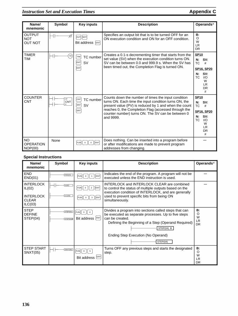
Instruction Set and Execution Times Appendix C
136
Name/mnemonic
Operands *DescriptionKey inputsSymbol
OUTPUTNOTOUT NOT ENT
NOT
Bit address
OUTSpecifies an output bit that is to be turned OFF for anON execution condition and ON for an OFF condition.
B:OWLRDR
TIMERTIM
TIM
ENT
TIM
ENT
TC number
SV
Creates a 0.1-s decrementing timer that starts from theset value (SV) when the execution condition turns ON.SV can be between 0.0 and 999.9 s. When the SV hasbeen timed out, the Completion Flag is turned ON.
SV:#
N:TC
SP10
SV:I/OWLRDR#
N:TC
SP16, SP20
COUNTERCNT
CP
RCNT
ENT
CNT
ENT
TC number
SV
Counts down the number of times the input conditionturns ON. Each time the input condition turns ON, thepresent value (PV) is reduced by 1 and when the countreaches 0, the Completion Flag (accessed through thecounter number) turns ON. The SV can be between 0and 9999.
SV:#
N:TC
SP10
SV:I/OWLRDR#
N:TC
SP16, SP20
NOOPERATIONNOP(00)
NoneFUN 0 0 ENT
Does nothing. Can be inserted into a program beforeor after modifications are made to prevent programaddresses from changing.
---
Special Instructions
Name/mnemonic
Symbol Key inputs Description Operands *
ENDEND(01)
END(01)FUN 0 ENT1
Indicates the end of the program. A program will not beexecuted unless the END instruction is used.
---
INTERLOCKIL(02)
INTERLOCKCLEARILC(03)
IL(02)
ILC(03)
FUN 0 ENT2
FUN 0 ENT3
INTERLOCK and INTERLOCK CLEAR are combinedto control the status of multiple outputs based on theexecution condition of INTERLOCK, and are generallyused to prevent specific bits from being ONsimultaneously.
---
STEPDEFINESTEP(04)
STEP(04)
STEP(04)B Bit address
FUN 0 4
ENT
Divides a program into sections called steps that canbe executed as separate processes. Up to five stepscan be created.
Defining the Beginning of a Step (Operand Required)
Ending Step Execution (No Operand)
STEP(04) B
STEP(04)
B:OWLRDR
STEP STARTSNXT(05)
SNXT(05)FUN 0
ENT
5
Bit address
Turns OFF any previous steps and starts the designatedstep.
B:OWLRDR
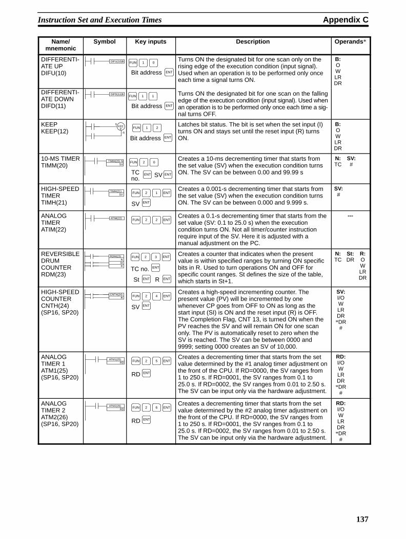
Appendix CInstruction Set and Execution Times
137
Name/mnemonic
Operands *DescriptionKey inputsSymbol
DIFFERENTI-ATE UPDIFU(10)
DIFU(10)B
Bit address
FUN
ENT
1 0Turns ON the designated bit for one scan only on therising edge of the execution condition (input signal).Used when an operation is to be performed only onceeach time a signal turns ON.
B:OWLRDR
DIFFERENTI-ATE DOWNDIFD(11)
DIFD(11)BFUN
ENT
1 1
Bit address
Turns ON the designated bit for one scan on the fallingedge of the execution condition (input signal). Used whenan operation is to be performed only once each time a sig-nal turns OFF.
KEEPKEEP(12)
KEEP
S
R
FUN 1 2
ENTBit address
Latches bit status. The bit is set when the set input (I)turns ON and stays set until the reset input (R) turnsON.
B:OWLRDR
10-MS TIMERTIMM(20)
TIMM(20) NSV
FUN 2 0
ENT ENTTCno.
SV
Creates a 10-ms decrementing timer that starts fromthe set value (SV) when the execution condition turnsON. The SV can be between 0.00 and 99.99 s
SV:#
N:TC
HIGH-SPEEDTIMERTIMH(21)
TIMH(21)SV FUN 2 1 ENT
ENTSV
Creates a 0.001-s decrementing timer that starts fromthe set value (SV) when the execution condition turnsON. The SV can be between 0.000 and 9.999 s.
SV:#
ANALOGTIMERATIM(22)
ATIM(22) FUN 2 2 ENTCreates a 0.1-s decrementing timer that starts from theset value (SV: 0.1 to 25.0 s) when the executioncondition turns ON. Not all timer/counter instructionrequire input of the SV. Here it is adjusted with amanual adjustment on the PC.
---
REVERSIBLEDRUMCOUNTERRDM(23)
RDM(23)NStR
FUN 2 ENT3
ENT
ENT ENTSt R
TC no.
Creates a counter that indicates when the presentvalue is within specified ranges by turning ON specificbits in R. Used to turn operations ON and OFF forspecific count ranges. St defines the size of the table,which starts in St+1.
St:DR
N:TC
R:OWLRDR
HIGH-SPEEDCOUNTERCNTH(24)(SP16, SP20)
CNTH(24)R FUN 2 4 ENT
ENTSV
Creates a high-speed incrementing counter. Thepresent value (PV) will be incremented by onewhenever CP goes from OFF to ON as long as thestart input (SI) is ON and the reset input (R) is OFF.The Completion Flag, CNT 13, is turned ON when thePV reaches the SV and will remain ON for one scanonly. The PV is automatically reset to zero when theSV is reached. The SV can be between 0000 and9999; setting 0000 creates an SV of 10,000.
SV:I/OWLRDR*DR
#
ANALOGTIMER 1ATM1(25)(SP16, SP20)
ATM1(25)RD FUN 2 5 ENT
ENTRD
Creates a decrementing timer that starts from the setvalue determined by the #1 analog timer adjustment onthe front of the CPU. If RD=0000, the SV ranges from1 to 250 s. If RD=0001, the SV ranges from 0.1 to25.0 s. If RD=0002, the SV ranges from 0.01 to 2.50 s.The SV can be input only via the hardware adjustment.
RD:I/OWLRDR*DR
#
ANALOGTIMER 2ATM2(26)(SP16, SP20)
ATM2(26)RD FUN 2 6 ENT
ENTRD
Creates a decrementing timer that starts from the setvalue determined by the #2 analog timer adjustment onthe front of the CPU. If RD=0000, the SV ranges from1 to 250 s. If RD=0001, the SV ranges from 0.1 to25.0 s. If RD=0002, the SV ranges from 0.01 to 2.50 s.The SV can be input only via the hardware adjustment.
RD:I/OWLRDR*DR
#
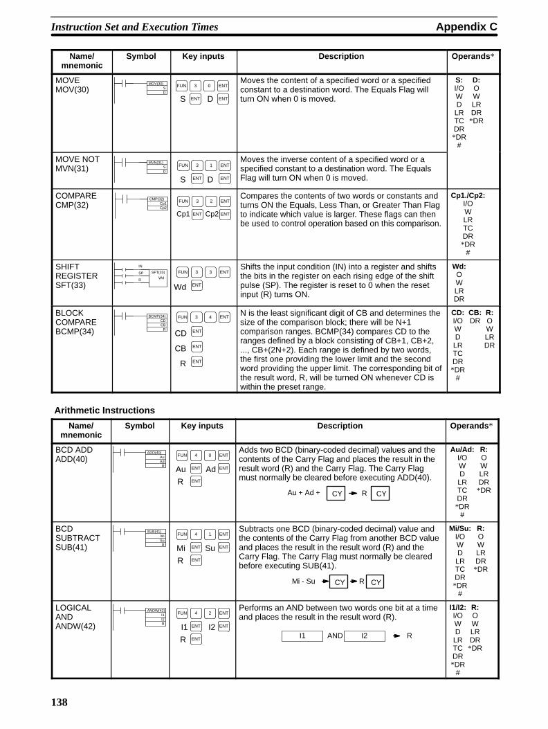
Instruction Set and Execution Times Appendix C
138
Name/mnemonic
Operands *DescriptionKey inputsSymbol
MOVEMOV(30)
MOV(30)SD
FUN 3 0 ENT
ENT ENTS D
Moves the content of a specified word or a specifiedconstant to a destination word. The Equals Flag willturn ON when 0 is moved.
D:OWLRDR*DR
S:I/OWDLRTCDR*DR
#
MOVE NOTMVN(31)
MVN(31)SD
FUN 3 ENT
ENT ENT
1
S D
Moves the inverse content of a specified word or aspecified constant to a destination word. The EqualsFlag will turn ON when 0 is moved.
COMPARECMP(32)
CMP(32)Cp1Cp2
FUN 3 ENT
ENT ENT
2
Cp1 Cp2
Compares the contents of two words or constants andturns ON the Equals, Less Than, or Greater Than Flagto indicate which value is larger. These flags can thenbe used to control operation based on this comparison.
Cp1./Cp2:I/OWLRTCDR*DR
#
SHIFTREGISTERSFT(33)
SFT(33)
Wd
IN
SP
R
FUN 3 3
ENT
ENT
Wd
Shifts the input condition (IN) into a register and shiftsthe bits in the register on each rising edge of the shiftpulse (SP). The register is reset to 0 when the resetinput (R) turns ON.
Wd:OWLRDR
BLOCKCOMPAREBCMP(34)
BCMP(34)CDCB
R
FUN 3 ENT4
ENTCDENTCBENTR
N is the least significant digit of CB and determines thesize of the comparison block; there will be N+1comparison ranges. BCMP(34) compares CD to theranges defined by a block consisting of CB+1, CB+2,..., CB+(2N+2). Each range is defined by two words,the first one providing the lower limit and the secondword providing the upper limit. The corresponding bit ofthe result word, R, will be turned ON whenever CD iswithin the preset range.
CB:DR
CD:I/OWDLRTCDR*DR
#
R:OWLRDR
Arithmetic Instructions
Name/mnemonic
Symbol Key inputs Description Operands *
BCD ADDADD(40)
ADD(40)AuAdR
FUN 4 0 ENT
ENTENT
ENT
Au Ad
R
Adds two BCD (binary-coded decimal) values and thecontents of the Carry Flag and places the result in theresult word (R) and the Carry Flag. The Carry Flagmust normally be cleared before executing ADD(40).
Au + Ad + RCY CY
R:OWLRDR*DR
Au/Ad:I/OWDLRTCDR*DR
#
BCDSUBTRACTSUB(41)
SUB(41)MiSuR
FUN 4 1 ENT
ENTENT
ENT
Mi Su
R
Subtracts one BCD (binary-coded decimal) value andthe contents of the Carry Flag from another BCD valueand places the result in the result word (R) and theCarry Flag. The Carry Flag must normally be clearedbefore executing SUB(41).
Mi - Su RCY CY
R:OWLRDR*DR
Mi/Su:I/OWDLRTCDR*DR
#
LOGICALANDANDW(42)
ANDW(42)I1I2R
FUN 4 2
ENT
ENT
ENT
ENTI1 I2
R
Performs an AND between two words one bit at a timeand places the result in the result word (R).
I1 RI2AND
R:OWLRDR*DR
I1/I2:I/OWDLRTCDR*DR
#

Appendix CInstruction Set and Execution Times
139
Name/mnemonic
Operands *DescriptionKey inputsSymbol
LOGICAL ORORW(43)
ORW(43)I1I2R
FUN 4 3
ENT
ENT
ENTENTI1 I2
R
Performs an OR between two words one bit at a timeand places the result in the result word (R).
I1 RI2OR
R:OWLRDR*DR
I1/I2:I/OWDLRTCDR*DR
#
CLEARCARRYCLC(44)
CLC(44)FUN 4 4 ENT
Resets the Carry Flag (bit 0312) to 0. Generally usedto clear the Carry Flag just before using ADD(40) orSUB(41).
---

Instruction Set and Execution Times Appendix C
140
Instruction Execution Times
The execution time is given in microseconds. “Word” indicates any data area address except for indirectly ad-dressed DR (*DR).
Instruction Number of words ON execution time Conditions OFF execution time
I/O, work, ordedicated
DR, LR, orTC (see
note)
I/O, work, ordedicated
LR, DR, orTC
LD 2 3 0.4 0.8 Always Same as ON time.
LD NOT 2 3 0.4 0.8 Always Same as ON time.
AND 1 2 0.2 0.6 Always Same as ON time.
AND NOT 1 2 0.2 0.6 Always Same as ON time.
OR 1 2 0.2 0.6 Always
OR NOT 1 2 0.2 0.6 Always Same as ON time.
AND LD 2 2 0.4 0.6 Always Same as ON time.
OR LD 2 2 0.4 0.6 Always Same as ON time.
OUT 2 3 2.4 7.0 Always Same as ON time.
OUT NOT 2 3 2.4 7.0 Always Same as ON time.
TIM --- 4 --- 24.4 Constant for SV R: 23.0IL: 24.8
38.5 Word for SV (SP16, SP20 only) R: 28.6IL 27 1
63.0 *DR for SV (SP16, SP20 only)IL: 27.1
CNT --- 4 --- 24.4 Constant for SV R: 22.4IL: 19.8
38.8 Word for SV (SP16, SP20 only) R: 28.9IL 4 8
63.0 *DR for SV (SP16, SP20 only)IL: 4.8
NOP(00) 1 1 0.2 Always N.A.
END(01) 1 1 9.8 Always N.A.
IL(02) 2 2 19.6 Always 19.8
ILC(03) 1 1 0.2 Always 0.2
STEP(04) 4 4 35.4 Always 23.0
SNXT(05) 4 4 38.2 Always 28.4
DIFU(10) 4 4 39.2 Always Normal: 32.8IL: 20.0
DIFD(11) 4 4 40.4 Always Normal: 34.4IL: 20.2
KEEP(12) 4 4 29.0 Always 28.4
TIMM(20) 4 4 29.5 Constant for SV R: 23.6IL: 22.2
25.8 Word for SV (SP16, SP20 only) R: 28.8IL 27 1
63.0 *DR for SV (SP16, SP20 only)IL: 27.1
TIMH(21) 4 4 26.0 Constant for SV R: 23.6IL: 22.2
22.8 Word for SV (SP16, SP20 only) R: 28.8IL 27 1
59.9 *DR for SV (SP16, SP20 only)IL: 27.1
ATIM(22) 3 3 24.8 Always R: 25.5IL: 23.9
RDM(23) 5 5 69.4 Always R: 68.0IL: 19.4
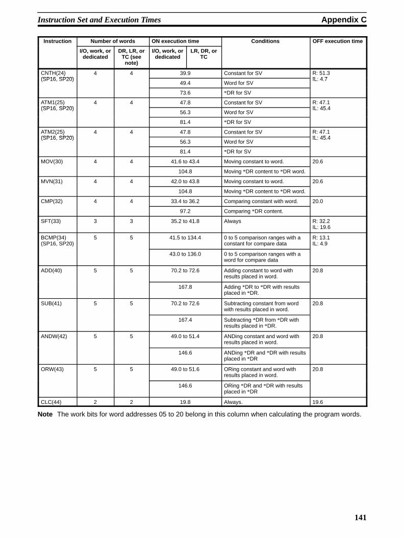
Appendix CInstruction Set and Execution Times
141
Instruction OFF execution timeConditionsON execution timeNumber of words
LR, DR, orTC
I/O, work, ordedicated
DR, LR, orTC (see
note)
I/O, work, ordedicated
CNTH(24)(SP16 SP20)
4 4 39.9 Constant for SV R: 51.3IL 4 7
( )(SP16, SP20)
49.4 Word for SVIL: 4.7
73.6 *DR for SV
ATM1(25)(SP16 SP20)
4 4 47.8 Constant for SV R: 47.1IL 45 4
( )(SP16, SP20)
56.3 Word for SVIL: 45.4
81.4 *DR for SV
ATM2(25)(SP16 SP20)
4 4 47.8 Constant for SV R: 47.1IL 45 4
( )(SP16, SP20)
56.3 Word for SVIL: 45.4
81.4 *DR for SV
MOV(30) 4 4 41.6 to 43.4 Moving constant to word. 20.6
104.8 Moving *DR content to *DR word.
MVN(31) 4 4 42.0 to 43.8 Moving constant to word. 20.6
104.8 Moving *DR content to *DR word.
CMP(32) 4 4 33.4 to 36.2 Comparing constant with word. 20.0
97.2 Comparing *DR content.
SFT(33) 3 3 35.2 to 41.8 Always R: 32.2IL: 19.6
BCMP(34)(SP16, SP20)
5 5 41.5 to 134.4 0 to 5 comparison ranges with aconstant for compare data
R: 13.1IL: 4.9
43.0 to 136.0 0 to 5 comparison ranges with aword for compare data
ADD(40) 5 5 70.2 to 72.6 Adding constant to word withresults placed in word.
20.8
167.8 Adding *DR to *DR with resultsplaced in *DR.
SUB(41) 5 5 70.2 to 72.6 Subtracting constant from wordwith results placed in word.
20.8
167.4 Subtracting *DR from *DR withresults placed in *DR.
ANDW(42) 5 5 49.0 to 51.4 ANDing constant and word withresults placed in word.
20.8
146.6 ANDing *DR and *DR with resultsplaced in *DR
ORW(43) 5 5 49.0 to 51.6 ORing constant and word withresults placed in word.
20.8
146.6 ORing *DR and *DR with resultsplaced in *DR
CLC(44) 2 2 19.8 Always. 19.6
Note The work bits for word addresses 05 to 20 belong in this column when calculating the program words.
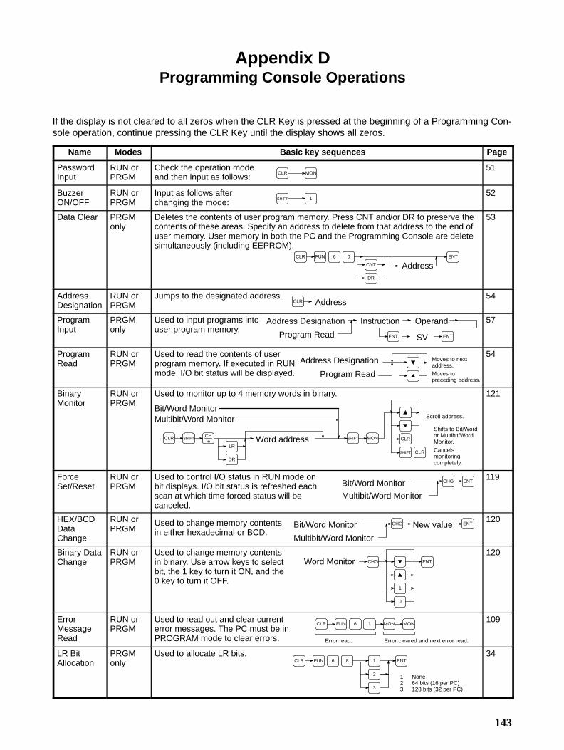
143
Appendix DProgramming Console Operations
If the display is not cleared to all zeros when the CLR Key is pressed at the beginning of a Programming Con-sole operation, continue pressing the CLR Key until the display shows all zeros.
Name Modes Basic key sequences Page
PasswordInput
RUN orPRGM
Check the operation modeand then input as follows:
CLR MON51
BuzzerON/OFF
RUN orPRGM
Input as follows afterchanging the mode:
1SHIFT52
Data Clear PRGMonly
Deletes the contents of user program memory. Press CNT and/or DR to preserve thecontents of these areas. Specify an address to delete from that address to the end ofuser memory. User memory in both the PC and the Programming Console are deletesimultaneously (including EEPROM).
AddressCLR FUN 6 0
CNT
DR
ENT
53
AddressDesignation
RUN orPRGM
Jumps to the designated address.CLR Address
54
ProgramInput
PRGMonly
Used to input programs intouser program memory.
Address Designation
SV
Instruction Operand
Program Read ENT ENT
57
ProgramRead
RUN orPRGM
Used to read the contents of userprogram memory. If executed in RUNmode, I/O bit status will be displayed.
Moves to nextaddress.Moves topreceding address.
Address Designation
Program Read
54
BinaryMonitor
RUN orPRGM
Used to monitor up to 4 memory words in binary.
Scroll address.
Shifts to Bit/Wordor Multibit/WordMonitor.
Cancelsmonitoringcompletely.
Word addressCLR SHIFT
LR
DR
SHIFT MON CLR
SHIFT CLR
Bit/Word MonitorMultibit/Word Monitor
CH
*
121
ForceSet/Reset
RUN orPRGM
Used to control I/O status in RUN mode onbit displays. I/O bit status is refreshed eachscan at which time forced status will becanceled.
CHG ENTBit/Word Monitor
Multibit/Word Monitor
119
HEX/BCDDataChange
RUN orPRGM
Used to change memory contentsin either hexadecimal or BCD.
New value ENTCHGBit/Word Monitor
Multibit/Word Monitor
120
Binary DataChange
RUN orPRGM
Used to change memory contentsin binary. Use arrow keys to selectbit, the 1 key to turn it ON, and the0 key to turn it OFF.
Word Monitor
0
1
ENTCHG
120
ErrorMessageRead
RUN orPRGM
Used to read out and clear currenterror messages. The PC must be inPROGRAM mode to clear errors. Error cleared and next error read.Error read.
CLR 1FUN 6 MON MON109
LR BitAllocation
PRGMonly
Used to allocate LR bits.
1: None2: 64 bits (16 per PC)3: 128 bits (32 per PC)
CLR FUN 6 18
2
3
ENT34
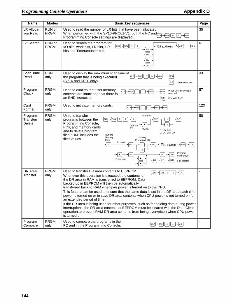
Programming Console Operations Appendix D
144
Name PageBasic key sequencesModes
LR Alloca-tion Read
RUN orPRGM
Used to read the number of LR bits that have been allocated.When performed with the SP10-PRO01-V1, both the PC andProgramming Console settings are displayed.
CLR FUN 6 MON9
35
Bit Search RUN orPRGM
Used to search the program forI/O bits, work bits, LR bits, HRbits and Timer/counter bits.
LR
DR
TIM
CNT
MONCLR FUN 07 MONBit address61
Scan TimeRead
RUNonly
Used to display the maximum scan time ofthe program that is being executed.(SP16 and SP20 only)
MONCLR FUN 37 MON
End with CLR.CLR
33
ProgramCheck
PRGMonly
Used to confirm that user memorycontents are intact and that there isan END instruction.
Press until END(01) isreached.
End with CLR.
CLR FUN 7 MON MON1
CLR
57
CardFormat
PRGMonly
Used to initialize memory cards.CLR FUN 7 2 ENT ENT
123
ProgramTransfer/Delete
PRGMonly
Used to transferprograms between theProgramming Console,PCs, and memory cardsand to delete programfiles. “UM” includes thefilter values.
File deleted.
File name
Programtransferred.
CLR FUN 26 1 ENT
2
1 ENT
2 ENT
2
1 ENT ENT
DEL
ENT
ENT
To/from PC
To/fromMemoryCard
1: UM only2: UM and DR
1: UM only2: UM and DR
To card
From card
To PC
From PC
ENT
CLR
CLR
CLR
58
DR AreaTransfer
PRGMonly
Used to transfer DR area contents to EEPROM.Whenever this operation is executed, the contents ofthe DR area in RAM is transferred to EEPROM. Databacked up in EEPROM will then be automaticallytransferred back to RAM whenever power is turned on to the CPU.This feature can be used to ensure that the same data is set in the DR area each timepower is turned on or to save DR area contents when CPU power is not turned on foran extended period of time.If the DR area is being used for other purposes, such as for holding data during powerinterruptions, the DR area contents of EEPROM must be cleared with the Data Clearoperation to prevent RAM DR area contents from being overwritten when CPU poweris turned on.
CLR FUN 6 3 ENT -
ProgramCompare
PRGMonly
Used to compare the programs in thePC and in the Programming Console. CLR FUN 6 MON4
-
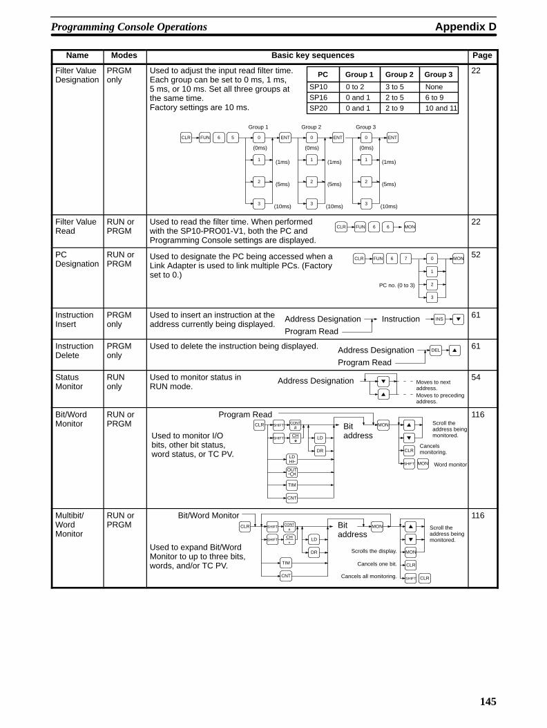
Appendix DProgramming Console Operations
145
Name PageBasic key sequencesModes
Filter ValueDesignation
PRGMonly
Used to adjust the input read filter time.Each group can be set to 0 ms, 1 ms,5 ms, or 10 ms. Set all three groups atthe same time.Factory settings are 10 ms.
Group 1
CLR FUN
1
2
3
ENT6 05
1
2
3
ENT0
(0ms) (0ms)
Group 2
(1ms)
(5ms)
(10ms)
(1ms)
(5ms)
(10ms)
SP10 0 to 2 3 to 5 None
SP16 0 and 1 2 to 5 6 to 9
SP20 0 and 1 2 to 9 10 and 11
Group 1 Group 2 Group 3PC
1
2
3
ENT0
(0ms)
Group 3
(1ms)
(5ms)
(10ms)
22
Filter ValueRead
RUN orPRGM
Used to read the filter time. When performedwith the SP10-PRO01-V1, both the PC andProgramming Console settings are displayed.
CLR FUN 6 6 MON22
PCDesignation
RUN orPRGM
Used to designate the PC being accessed when aLink Adapter is used to link multiple PCs. (Factoryset to 0.)
PC no. (0 to 3)
MONCLR FUN 6 7
1
2
3
052
InstructionInsert
PRGMonly
Used to insert an instruction at theaddress currently being displayed.
Address Designation
Program Read
Instruction INS61
InstructionDelete
PRGMonly
Used to delete the instruction being displayed. Address Designation
Program Read
DEL61
StatusMonitor
RUNonly
Used to monitor status inRUN mode.
Moves to precedingaddress.
Moves to nextaddress.
Address Designation 54
Bit/WordMonitor
RUN orPRGM
Used to monitor I/Obits, other bit status,word status, or TC PV.
Cancelsmonitoring.
TIM
CNT
CLR MONSHIFT
SHIFT LD
DR CLR
SHIFT MONLD
OUT
CONT#
CH
*
Program ReadBitaddress
Scroll theaddress beingmonitored.
Word monitor
116
Multibit/WordMonitor
RUN orPRGM
Used to expand Bit/WordMonitor to up to three bits,words, and/or TC PV.
Scrolls the display.
Scroll theaddress beingmonitored.
Cancels one bit.
Cancels all monitoring.
TIM
CNT
CLR MONSHIFT
SHIFTCH*
LD
DR
CLR
MON
CLR
SHIFT
CONT#
Bit/Word MonitorBitaddress
116

147
Appendix EError and Arithmetic Flag Operation
The following table shows the instructions that affect the ER, CY, GT, LT and EQ flags. In general, ER indi-cates that operand data is not within requirements. CY indicates arithmetic or data shift results. GT indicatesthat a compared value is larger than some standard, LT that it is smaller, and EQ, that it is the same. EQ alsoindicates a result of zero for arithmetic operations. Refer to Section 3 Instruction Set for details.
Vertical arrows in the table indicate the flags that are turned ON and OFF according to the result of the in-struction.
Although timer and counter instructions are executed when ER is ON, instructions with a vertical arrow underthe ER column are not executed if ER is ON. All of the other flags in the following table will also not operatewhen ER is ON.
Instructions 0311 (ER) 0312 (CY) 0313 (LT) 0314 (EQ) 0315 (GT)
TIM Unaffected Unaffected Unaffected Unaffected Unaffected
CNT Unaffected Unaffected Unaffected Unaffected Unaffected
END(01) OFF OFF OFF OFF OFF
STEP(04) Unaffected Unaffected Unaffected Unaffected
SNXT(05) Unaffected Unaffected Unaffected Unaffected
TIMM(20) Unaffected Unaffected Unaffected Unaffected Unaffected
TIMH(21) Unaffected Unaffected Unaffected Unaffected Unaffected
ATIM(22) Unaffected Unaffected Unaffected Unaffected Unaffected
RDM(23) Unaffected Unaffected Unaffected Unaffected
CNTH(24) Unaffected Unaffected Unaffected Unaffected
ATM1(25) Unaffected Unaffected Unaffected Unaffected Unaffected
ATM2(26) Unaffected Unaffected Unaffected Unaffected Unaffected
MOV(30) Unaffected Unaffected Unaffected
MVN(31) Unaffected Unaffected Unaffected
CMP(32) Unaffected
SFT(33) Unaffected Unaffected Unaffected Unaffected
BCMP(34) Unaffected Unaffected Unaffected Unaffected
ADD(40) Unaffected Unaffected
SUB(41) Unaffected Unaffected
ANDW(42) Unaffected Unaffected Unaffected
ORW(43) Unaffected Unaffected Unaffected
CLC(44) Unaffected OFF Unaffected Unaffected Unaffected

149
Appendix FI/O Assignment Sheets
This appendix contains sheets that can be copied by the programmer to record I/O bit allocations and terminalassignments, as well as details of work bits, data storage areas, timers, and counters.
Some bits appear as both I/O bits and work bits so that the I/O assignment sheets can be used forany of the SP-series PCs. Be sure that you do not assign a bit as a work bit if it is already beingused as an I/O bit and that you do not assign more I/O bits than are supported by your PC.
Note
I/O Assignment Sheets Appendix F
150
No.: System:
Program: Programmer: Date:
Unit #0Inputs
Bit Field device Notes
0000
0001
0002
0003
0004
0005
0006
0007
0008
0009
0010
0011
Outputs
Bit Field device Notes
0100
0101
0102
0103
0104
0105
0106
0107
Unit #1Inputs
Bit Field device Notes
0000
0001
0002
0003
0004
0005
0006
0007
0008
0009
0010
0011
Outputs
Bit Field device Notes
0100
0101
0102
0103
0104
0105
0106
0107
I/O Bits

Appendix FI/O Assignment Records Sheets
151
No.: System:
Program: Programmer: Date:
Unit #2Inputs
Bit Field device Notes
0000
0001
0002
0003
0004
0005
0006
0007
0008
0009
0010
0011
Outputs
Bit Field device Notes
0100
0101
0102
0103
0104
0105
0106
0107
Unit #3Inputs
Bit Field device Notes
0000
0001
0002
0003
0004
0005
0006
0007
0008
0009
0010
0011
Outputs
Bit Field device Notes
0100
0101
0102
0103
0104
0105
0106
0107
I/O Bits
I/O Assignment Sheets Appendix F
152
No.: System:
Programmer: Program: Date: Unit #:
Timers and Counters
Address T or C Set value Notes
00
01
01
03
04
05
06
07
08
09
10
11
12
13
14
15
Word 00
Bit Usage Notes
0008
0009
0010
0011
0012
0013
0014
0015
Word 01
Bit Usage Notes
0104
0105
0106
0107
0108
0109
0110
0111
0112
0113
0114
0115
Word 02
Bit Usage Notes
0200
0201
0202
0203
0204
0205
0206
0207
0208
0209
0210
0211
0212
0213
0214
0215
TC Area and Work Bits
Appendix FI/O Assignment Records Sheets
153
Word:
Bit Usage Notes
00
01
02
03
04
05
06
07
08
09
10
11
12
13
14
15
Word:
Bit Usage Notes
00
01
02
03
04
05
06
07
08
09
10
11
12
13
14
15
Word:
Bit Usage Notes
00
01
02
03
04
05
06
07
08
09
10
11
12
13
14
15
Word:
Bit Usage Notes
00
01
02
03
04
05
06
07
08
09
10
11
12
13
14
15
TC Area and Work Bits
I/O Assignment Sheets Appendix F
154
No.: System:
Programmer: Program: Date: Unit #:
Word Contents Notes Word Contents Notes
Data Storage

155
Appendix GProgram Coding Sheet
The following pages can be copied for use in coding ladder diagram programs.
When coding programs, be sure to specify all function codes for instructions and data areas (or # for constant)for operands. These will be necessary when inputting programs though a Programming Console or other Pe-ripheral Device.
Program Coding Sheet Appendix G
156
No.: System: Page 1
Program: Programmer: Date:
Address Instruction Operand(s)
000
001
002
003
004
005
006
007
008
009
010
011
012
013
014
015
016
017
018
019
020
021
022
023
024
025
026
027
028
029
030
031
032
033
034
035
036
037
Address Instruction Operand(s)
038
039
040
041
042
043
044
045
046
047
048
049
050
051
052
053
054
055
056
057
058
059
060
061
062
063
064
065
066
067
068
069
070
071
072
073
074
075
Appendix GProgram Coding Sheet
157
No.: System: Page 2
Program: Programmer: Date:
Address Instruction Operand(s)
076
077
078
079
080
081
082
083
084
085
086
087
088
089
090
091
092
093
094
095
096
097
098
099
100
101
102
103
104
105
106
107
108
109
110
111
112
113
Address Instruction Operand(s)
114
115
116
117
118
119
120
121
122
123
124
125
126
127
128
129
130
131
132
133
134
135
136
137
138
139
140
141
142
143
144
145
146
147
148
149
150
151
Program Coding Sheet Appendix G
158
No.: System: Page 3
Program: Programmer: Date:
Address Instruction Operand(s)
152
153
154
155
156
157
158
159
160
161
162
163
164
165
166
167
168
169
170
171
172
173
174
175
176
177
178
179
180
181
182
183
184
185
186
187
188
189
Address Instruction Operand(s)
190
191
192
193
194
195
196
197
198
199
200
201
202
203
204
205
206
207
208
209
210
211
212
213
214
215
216
217
218
219
220
221
222
223
224
225
226
227

Appendix GProgram Coding Sheet
159
No.: System: Page 4
Program: Programmer: Date:
Address Instruction Operand(s)
228
229
230
231
232
233
234
235
236
237
238
239
240
241
242
243
244
245
246
247
248
249
250
251
252
253
254
255
256
257
258
259
260
261
262
263
264
265
Address Instruction Operand(s)
266
267
268
269
270
271
272
273
274
275
276
277
278
279
280
281
282
283
284
285
286
287
288
289
290
291
292
293
294
295
296
297
298
299
300
301
302
303
Program Coding Sheet Appendix G
160
No.: System: Page 5
Program: Programmer: Date:
Address Instruction Operand(s)
304
305
306
307
308
309
310
311
312
313
314
315
316
317
318
319
320
321
322
323
324
325
326
Address Instruction Operand(s)
327
328
329
330
331
332
333
334
335
336
337
338
339
340
341
342
343
344
345
346
347
348
161
Glossary
address The location in memory where data is stored. For data areas, an addressconsists of a two-letter data area designation and a number that designatesthe word and/or bit location. For the UM area, an address designates theinstruction location (UM area).
allocation The process by which the PC assigns certain bits or words in memory forvarious functions. This includes pairing I/O bits to I/O points.
AND A logic operation whereby the result is true if and only if both premises aretrue. In ladder-diagram programming the premises are usually ON/OFFstates of bits or the logical combination of such states called execution condi-tions.
BCD Short for binary-coded decimal.
BCD calculation An arithmetic calculation that uses numbers expressed in binary-coded deci-mal.
binary A number system where all numbers are expressed to the base 2, i.e., anynumber can be written using only 1’s or 2’s. Each group of four binary bits isequivalent to one hexadecimal digit.
binary calculation An arithmetic calculation that uses numbers expressed in binary.
binary-coded decimal A system used to represent numbers so that each group of four binary bits isnumerically equivalent to one decimal digit.
bit A binary digit; hence a unit of data in binary notation. The smallest unit ofinformation that can be electronically stored in a PC. The status of a bit iseither ON or OFF. Different bits at particular addresses are allocated to spe-cial purposes, such as holding the status input from external devices, whileother bits are available for general use in programming.
bit address The location in memory where a bit of data is stored. A bit address mustspecify (sometimes by default) the data area and word that is being ad-dressed, as well as the number of the bit.
bit number A number that indicates the location of a bit within a word. Bit 00 is the right-most (least-significant) bit; bit 15 is the leftmost (most-significant) bit.
bus bar The line leading down the left and sometimes right side of a ladder diagram.Instruction execution proceeds down the bus bar, which is the starting pointfor all instruction lines.
carry flag A flag that is used with arithmetic operations to hold a carry from an additionor multiplication operation, or to indicate that the result is negative in a sub-traction operation. The carry flag is also used with certain types of shift op-erations.
clock pulse A pulse available at a certain bit in memory for use in timing operations. Vari-ous clock pulses are available with different pulse widths.
Glossary
162
clock pulse bit A bit in memory that supplies a pulse that can be used to time operations.Various clock pulse bits are available with different pulse widths, and there-fore different frequencies.
common data Data that is stored in the LR Area of a PC and which is shared by other PCsin the same the same system. Each PC has a specified section of the LRArea allocated to it. This allocation is the same in each LR Area of each PC.
condition An message placed in an instruction line to direct the way in which the termi-nal instructions, on the right side, are to be executed. Each condition is as-signed to a bit in memory that determines its status. The status of the bit as-signed to each condition determines, in turn, the execution condition for eachinstruction up to a terminal instruction on the right side of the ladder diagram.
constant An operand for which the actual numeric value is specified by the user, andwhich is then stored in a particular address in the data memory.
control bit A bit in a memory area that is set either through the program or via a Pro-gramming Device to achieve a specific purpose, e.g., a Restart bit is turnedON and OFF to restart a Unit.
Control System All of the hardware and software components used to control other devices.A Control System includes the PC System, the PC programs, and all I/O de-vices that are used to control or obtain feedback from the controlled system.
controlled system The devices that are being controlled by a PC System.
control signal A signal sent from the PC to effect the operation of the controlled system.
counter A dedicated group of digits or words in memory used to count the number oftimes a specific process has occurred, or a location in memory accessedthrough a TC bit and used to count the number of times the status of a bit oran execution condition has changed from OFF to ON.
CPU An acronym for central processing unit. In a PC System, the CPU executesthe program, processes I/O signals, communicates with external devices,etc.
data area An area in the PC’s memory that is designed to hold a specific type of data,e.g., the LR area is designed to hold common data in a PC Link System.Memory areas that hold programs are not considered data areas.
data area boundary The highest address available within a data area. When designating an oper-and that requires multiple words, it is necessary to ensure that the highestaddress in the data area is not exceeded.
data sharing An aspect of Data Links created through Link Adapters in which commondata areas or common data words are created between two or more PCs.
debug A process by which a draft program is corrected until it operates as intended.Debugging includes both the removal of syntax errors, as well as the fine-tuning of timing and coordination of control operations.
decimal A number system where all numbers are expressed to the base 10. In a PCall data is ultimately stored in binary form, four binary bits are often used torepresent one decimal digit, via a system called binary-coded decimal.

Glossary
163
decrement Decreasing a numeric value.
default A value automatically set by the PC when the user omits to set a specific val-ue. Many devices will assume such default conditions upon the application ofpower.
delay In tracing, a value that specifies where tracing is to begin in relationship tothe trigger. A delay can be either positive or negative, i.e., can designate anoffset on either side of the trigger.
destination The location where an instruction is to place the data on which it is operating,as opposed to the location from which data is taken for use in the instruction.The location from which data is taken is called the source.
differentiated instruction An instruction used to ensure that the operand bit is never turned ON formore than one scan after the execution condition goes either from OFF toON for a Differentiate Up instruction or from ON to OFF for a DifferentiateDown instruction.
digit A unit of storage in memory that consists of four bits.
distributed control An automation concept in which control of each portion of an automated sys-tem is located near the devices actually being controlled, i.e., control is de-centralized and ‘distributed’ over the system. Distributed control is one of thefundamental concepts of PC Systems.
download The process of transferring a program or data from a higher-level computerto a lower-level computer or PC or between peripheral devices and the PC.
electrical noise Random variations of one or more electrical characteristics such as voltage,current, and data, which might interfere with the normal operation of a de-vice.
execution condition The ON or OFF status under which an instruction is executed. The executioncondition is determined by the logical combination of conditions on the sameinstruction line and up to the instruction currently being executed.
execution time The time required for the CPU to execute either an individual instruction oran entire program.
extended counter A counter created in a program by using two or more count instructions insuccession. Such a counter is capable of counting higher than any of thestandard counters provided by the individual instructions.
extended timer A timer created in a program by using two or more timers in succession.Such a timer is capable of timing longer than any of the standard timers pro-vided by the individual instructions.
fatal error An error that stops PC operation and requires correction before operationcan continue.
flag A dedicated bit in memory that is set by the system to indicate some type ofoperating status. Some flags, such as the carry flag, can also be set by theoperator or via the program.
Glossary
164
flicker bit A bit that is programmed to turn ON and OFF at a specific frequency.
force reset The process of forcibly turning OFF a bit via a programming device. Bits areusually turned OFF as a result of program execution.
force set The process of forcibly turning ON a bit via a programming device. Bits areusually turned ON as a result of program execution.
function code A two-digit number used to input an instruction into the PC.
hardware error An error originating in the hardware structure (electronic components) of thePC, as opposed to a software error, which originates in software (i.e., pro-grams).
hexadecimal A number system where all numbers are expressed to the base 16. In a PCall data is ultimately stored in binary form, however, displays and inputs onProgramming Devices are often expressed in hexadecimal to simplify opera-tion. Each group of four binary bits is numerically equivalent to one hexadeci-mal digit.
increment Increasing a numeric value.
indirect address An address whose contents indicates another address. The contents of thesecond address will be used as the operand. Indirect addressing is possiblein the DR area only .
initialize Part of the startup process whereby some memory areas are cleared, systemsetup is checked, and default values are set.
input The signal coming from an external device into the PC. The term input isoften used abstractly or collectively to refer to incoming signals.
input bit A bit that is allocated to hold the status of an input.
input device An external device that sends signals into the PC System.
input point The point at which an input enters the PC System. Input points correspondphysically to terminals or connector pins.
input signal A change in the status of a connection entering the PC. Generally an inputsignal is said to exist when, for example, a connection point goes from low tohigh voltage or from a nonconductive to a conductive state.
instruction A direction given in the program that tells the PC of an action to be carriedout, and which data is to be used in carrying out the action. Instructions canbe used to simply turn a bit ON or OFF, or they can perform much more com-plex actions, such as converting and/or transferring large blocks of data.
instruction block A group of instructions that is logically related in a ladder-diagram program.Although any logically related group of instructions could be called an instruc-tion block, the term is generally used to refer to blocks of instructions calledlogic blocks that require logic block instructions to relate them to otherinstructions or logic blocks.
instruction execution time The time required to execute an instruction. The execution time for any oneinstruction can vary with the execution conditions for the instruction and theoperands used within it.

Glossary
165
instruction line A group of conditions that lie together on the same horizontal line of a ladderdiagram. Instruction lines can branch apart or join together to form instructionblocks.
interlock A programming method used to treat a number of instructions as a group sothat the entire group can be reset together when individual execution is notrequired. An interlocked program section is executed normally for an ONexecution condition and partially reset for an OFF execution condition.
I/O capacity The number of inputs and outputs that a PC is able to handle. This numberranges from around 10 for smaller PCs to two thousand for the largest ones.
I/O devices The devices to which terminals on I/O Units or Special I/O Units, or otherUnits are connected. I/O devices may be either part of the Control System, ifthey function to help control other devices, or they may be part of the con-trolled system.
I/O point The place at which an input signal enters the PC System, or at which an out-put signal leaves the PC System. In physical terms, I/O points correspond toterminals or connector pins on a Unit; in terms of programming, an I/O pointscorrespond to I/O bits in memory.
I/O response time The time required for an output signal to be sent from the PC in response toan input signal received from an external device.
JIS Acronym for Japanese Industrial Standards.
ladder diagram (program) A form of program arising out of relay-based control systems that uses cir-cuit-type diagrams to represent the logic flow of programming instructions.The appearance of the program is similar to a ladder, and thus the name.
ladder diagram symbol A symbol used in a ladder-diagram program.
ladder instruction An instruction that represents the ‘rung’ portion of a ladder-diagram program.The other instructions in a ladder diagram fall along the right side of the dia-gram and are called terminal instructions.
leftmost (bit/word) The highest numbered bits of a group of bits, generally of an entire word, orthe highest numbered words of a group of words. These bits/words are oftencalled most-significant bits/words.
Link Adapter A Unit used to connect up to four CPUs to enable created data links in the LRarea.
logic block A group of instructions that is logically related in a ladder-diagram programand that requires logic block instructions to relate it to other instructions orlogic blocks.
logic block instruction An instruction used to locally combine the execution condition resulting froma logic block with a current execution condition. The current execution condi-tion could be the result of a single condition, or of another logic block. ANDLoad and OR Load are the two logic block instructions.
logic instruction Instructions used to logically combine the content of two words and outputthe logical results to a specified result word. The logic instructions combine

Glossary
166
all the same-numbered bits in the two words and output the result to the bit ofthe same number in the specified result word.
memory area Any of the areas in the PC used to hold data or programs.
mnemonic code A form of a ladder-diagram program that consists of a sequential list of theinstructions without using a ladder diagram. Mnemonic code is required toinput a program into a PC when using a Programming Console.
most-significant (bit/word) See leftmost (bit/word).
NC input An input that is normally closed, i.e., the input signal is considered to bepresent when the circuit connected to the input opens.
NO input An input that is normally open, i.e., the input signal is considered to be pres-ent when the circuit connected to the input closes.
noise interference Disturbances in signals caused by electrical noise.
nonfatal error A hardware or software error that produces a warning but does not stop thePC from operating.
normally closed condition A condition that produces an ON execution condition when the bit assignedto it is OFF, and an OFF execution condition when the bit assigned to it isON.
normally closed condition A condition that produces an ON execution condition when the bit assignedto it is ON, and an OFF execution condition when the bit assigned to it isOFF.
NOT A logic operation which inverts the status of the operand. For example, ANDNOT indicates an AND operation with the opposite of the actual status of theoperand bit.
OFF The status of an input or output when a signal is said not to be present. TheOFF state is generally represented by a low voltage or by non-conductivity,but can be defined as the opposite of either.
OFF delay The delay between the time when a signal is switched OFF (e.g., by an inputdevice or PC) and the time when the signal reaches a state readable as anOFF signal (i.e., as no signal) by a receiving party (e.g., output device orPC).
ON The status of an input or output when a signal is said to be present. The ONstate is generally represented by a high voltage or by conductivity, but can bedefined as the opposite of either.
ON delay The delay between the time when an ON signal is initiated (e.g., by an inputdevice or PC) and the time when the signal reaches a state readable as anON signal by a receiving party (e.g., output device or PC).
one-shot bit A bit that is turned ON or OFF for a specified interval of time which is longerthan one scan.
operand Bit(s) or word(s) designated as the data to be used for an instruction. An op-erand can be input as a constant expressing the actual numeric value to be
Glossary
167
used or as an address to express the location in memory of the data to beused.
operand bit A bit designated as an operand for an instruction.
operand word A word designated as an operand for an instruction.
operating error An error that occurs during actual PC operation as opposed to an initializa-tion error, which occurs before actual operations can begin.
OR A logic operation whereby the result is true if either of two premises is true, orif both are true. In ladder-diagram programming the premises are usually ON/OFF states of bits or the logical combination of such states called executionconditions.
output The signal sent from the PC to an external device. The term output is oftenused abstractly or collectively to refer to outgoing signals.
output bit A bit in memory that is allocated to hold the status to be sent to an outputdevice.
output device An external device that receives signals from the PC System.
output point The point at which an output leaves the PC System. Output points corre-spond physically to terminals or connector pins.
output signal A signal being sent to an external device. Generally an output signal is saidto exist when, for example, a connection point goes from low to high voltageor from a nonconductive to a conductive state.
overseeing Part of the processing performed by the CPU that includes general tasks re-quired to operate the PC.
overwrite Changing the content of a memory location so that the previous content islost.
PC An acronym for Programmable Controller.
PC configuration The arrangement and interconnections of the Units that are put together toform a functional PC.
peripheral device Devices connected to a PC System to aid in system operation. Peripheraldevices include printers, programming devices, external storage media, etc.
port A connector on a PC or computer that serves as a connection to an externaldevice.
present value The current value registered in a device at any instant during its operation.Present value is abbreviated as PV.
printed circuit board A board onto which electrical circuits are printed for mounting into a comput-er or electrical device.
program The list of instructions that tells the PC the sequence of control actions to becarried out.
Glossary
168
Programmable Controller A computerized device that can accept inputs from external devices and gen-erate outputs to external devices according to a program held in memory.Programmable Controllers are used to automate control of external devices.Although single-component Programmable Controllers are available, build-ing-block Programmable Controllers are constructed from separate compo-nents. Such building-block Programmable Controllers are formed only whenenough of these separate components are assembled to form a functionalassembly, i.e., no one individual Unit is called a PC.
programmed alarm An alarm given as a result of execution of an instruction designed to gener-ate the alarm in the program, as opposed to one generated by the system.
programmed error An error arising as a result of the execution of an instruction designed to gen-erate the error in the program, as opposed to one generated by the system.
programmed message A message generated as a result of execution of an instruction designed togenerate the message in the program, as opposed to one generated by thesystem.
Programming Console The simplest form or programming device available for a PC. ProgrammingConsoles are available both as hand-held models and, for larger PCs, asCPU-mounting models.
PROGRAM mode A mode of operation that allows inputting and debugging of programs to becarried out, but that does not permit normal execution of the program.
PV Acronym for present value.
refresh The process of updating output status sent to external devices so that itagrees with the status of output bits held in memory and of updating inputbits in memory so that they agree with the status of inputs from external de-vices.
relay-based control The forerunner of PCs. In relay-based control, groups of relays are intercon-nected to form control circuits. In a PC, these are replaced by programmablecircuits.
reset The process of turning a bit or signal OFF or of changing the present value ofa timer or counter to its set value or to zero.
return The process by which instruction execution shifts from a subroutine back tothe main program (usually the point from which the subroutine was called).
reversible counter A counter that can be both incremented and decremented depending on thespecified conditions.
right-hand instruction Another term for terminal instruction.
rightmost (bit/word) The lowest numbered bits of a group of bits, generally of an entire word, orthe lowest numbered words of a group of words. These bits/words are oftencalled least-significant bits/words.
RUN mode The operating mode used by the PC for normal control operations.
scan The process used to execute a ladder-diagram program. The program is ex-amined sequentially from start to finish and each instruction is executed inturn based on execution conditions.
Glossary
169
scan time The time required for a single scan of the ladder-diagram program.
self diagnosis A process whereby the system checks its own operation and generates awarning or error if an abnormality is discovered.
self-maintaining bit A bit that is programmed to maintain either an OFF or ON status until set orreset by specified conditions.
set The process of turning a bit or signal ON.
set value The value from which a decrementing counter starts counting down or towhich an incrementing counter counts up (i.e., the maximum count), or thetime from which or for which a timer starts timing. Set value is abbreviatedSV.
shift register One or more words in which data is shifted a specified number of units to theright or left in bit, digit, or word units. In a rotate register, data shifted out oneend is shifted back into the other end. In other shift registers, new data (ei-ther specified data, zero(s) or one(s)) is shifted into one end and the datashifted out at the other end is lost.
slot A position on a Rack (Backplane) to which a Unit can be mounted.
software error An error that originates in a software program.
source The location from which data is taken for use in an instruction, as opposed tothe location to which the result of an instruction is to be written. The latter iscalled the destination.
SV Abbreviation for set value.
switching capacity The maximum voltage/current that a relay can safely switch on and off.
syntax error An error in the way in which a program is written. Syntax errors can include‘spelling’ mistakes (i.e., a function code that does not exist), mistakes inspecifying operands within acceptable parameters (e.g., specifying reservedSR bits as a destination), and mistakes in actual application of instructions(e.g., a call to a subroutine that does not exist).
system configuration The arrangement in which Units in a system are connected.
system error An error generated by the system, as opposed to one resulting from execu-tion of an instruction designed to generate an error.
system error message An error message generated by the system, as opposed to one resultingfrom execution of an instruction designed to generate a message.
TC area A data area that can be used only for timers and counters. Each bit in the TCarea serves as the access point for the SV, PV, and Completion Flag for thetimer or counter defined with that bit.
TC number A definer that corresponds to a bit in the TC area and used to define the bitas either a timer or a counter.
terminal instruction An instruction placed on the right side of a ladder diagram that uses the finalexecution conditions of an instruction line.
Glossary
170
timer A location in memory accessed through a TC bit and used to time down fromthe timer’s set value. Timers are turned ON and reset according to theirexecution conditions.
transfer The process of moving data from one location to another within the PC, orbetween the PC and external devices. When data is transferred, generally acopy of the data is sent to the destination, i.e., the content of the source ofthe transfer is not changed.
UM area The memory area used to hold the active program, i.e., the program that isbeing currently executed.
watchdog timer A timer within the system that ensures that the scan time stays within speci-fied limits. When limits are reached, either warnings are given or PC opera-tion is stopped depending on the particular limit that is reached.
word A unit of data storage in memory that consists of 16 bits. All data areas con-sists of words. Some data areas can be accessed only by words; others, byeither words or bits.
word address The location in memory where a word of data is stored. A word address mustspecify (sometimes by default) the data area and the number of the word thatis being addressed.
work bit A bit that can be used for data calculation or other manipulation in program-ming, i.e., a ‘work space’ in memory.

171
Index
Aaddressing, nomenclature, 28 analog timers, set value, 33 arithmetic flags, 71
Bbackup, program and data, 5870 BCDconverting, 29 definition, 29
binary, definition, 29 bitsforced setting/resetting, 119 monitoring, 116
Cchannel. See wordconstants, operands, 72 control bits, DR Data Transfer Enable Bit, 33 Control System, definition, 4 controlled system, definition, 4 counters, 81 bits in TC area, 36 conditions when reset, 90 creating extended timers, 91 extended, 91 inputting SV, 56
CPUsdimensions, 12 I/O wiring, 16 operational flow, 110111 power supply wiring, 15
Current Scan Time Area, 33
Ddataconverting, 29 modifying, 116 binary, 122 hex/BCD, 120
data areasspecial relay areaarithmetic flags, operation, 147 error flag, operation, 147
structure, 28 data retentionin DR area, 36 in TC area, 36
debugging, 109110 decimal point, 30
dedicated bit, definition, 31 definers, definition, 71 digit numbers, 29 dimensionsDIN Track, 13 for mounting, 13 Link Adapter, 12 PC, 12 Programming Console, 12
DIN Trackconnecting Units, 15 dimensions, 13
DR area, 36 relationship to LR area, 34
Eenvironmentambient temperature, 14 humidity, 14 installation, 13 noise, 14
errorsclearing messages, 54 dedicated bit area flags, 129 during program input, 129 fatal errors, 129 memory card initialization, 125 message tables, 128129 messages when inputting programs, 57 PC indicators, 128 reading and clearing messages, 109 , 128
execution condition, definition, 41
Ffilters, 22 flagsAlways ON/OFF, 33 arithmetic, 32 CY, 33 EQ, 33 GR, 33 LE, 33 programming example, 99
CY, clearing, 102 dedicated bit area errors, 129 Error, 32 First Scan, 33 Step, 33
forced setting/resetting, 119 function codes, 71
Hhexadecimal, definition, 29
Index
172
II/O bit, definition, 30 I/O response times, 111 I/O wiring diagrams, 16 , 17 , 18 , 19 indirect addressing, 30 , 72 input bit, definition, 3 input device, definition, 3 input devices, 19 input point, definition, 3 input signaldefinition, 3 filtering, 22
instruction execution times, 140 instruction setADD(40), 102 AND, 42 , 74 combining with OR, 43
AND LD, 45 , 75 combining with OR LD, 47 use in logic blocks, 46
AND NOT, 42 , 74 ANDW(42), 105 ATIM(22), 87 ATM1(25), 88 ATM2(26), 88 BCMP(34), 101 CLC(44), 102 CMP(32), 99 CNT, 89 CNTH(24), 94 DIFD(11), 66 , 7677 using in interlocks, 80
DIFU(10), 66 , 7677 using in interlocks, 80
END(01), 44 , 74 , 81 IL(02), 64 , 79108 ILC(03), 64 , 79108 KEEP(12), 78 in controlling bit status, 66
LD, 42 , 74 LD NOT, 42 , 74 MOV(30), 98 MVN(31), 98 NOP(00), 81 NOT, 40 OR, 43 , 74 combining with AND, 43
OR LD, 46 , 75 combining with AND LD, 47 use in logic blocks, 46
OR NOT, 43 , 74 ORW(43), 105 OUT, 44 , 75 OUT NOT, 44 , 75 RDM(23), 92 SFT(33), 96 STEP(04), 106 SUB(41), 103 SVXT(05), 106 TIM, 83 TIMH(21), 87
TIMM(20), 86 instructionsdesignation function codes, 56 table, 135 terminology, 39
interlocks, 79108 converting to mnemonic code, 80 using selfmaintaining bits, 67
Lladder diagrambranching, 64 IL(02) and ILC(03), 64
controlling bit statususing DIFU(10) and DIFD(11), 66 , 7677 using KEEP(12), 7879 using OUT and OUT NOT, 44
converting to mnemonic code, 4151 instructionscombining, AND LD and OR LD, 47 controlling bit statususing KEEP(12), 66 using OUT and OUT NOT, 75
format, 71 notation, 71 using logic blocks, 45
ladder instructions, 42 leftmost, definition, 28 Link Adapter, 7 dimensions, 12
logic block instructions, converting to mnemonic code,4550
logic blocks. See ladder diagramLR area, 33 allocation, 34 relationship to DR area, 34
MMaximum Scan Time Area, 33 memory areasclearing, 53 partial clear, 54
Memory Card, 7 battery replacement, 7 initialization, 123
mnemonic code, converting, 4151 model numbers, 131 modifying databinary, 122 bit forced set/reset, 119 general, 116 hex/BCD, 120
monitoringbinary, 121 bits, 116119 general, 116 multiple addresses, 116 , 119 PC selection, 52

Index
173
words, 116119 mountingDIN Track, 15 surface, 13
Nnormally closed condition, definition, 40 NOT, definition, 40
Ooperand bit, 41 operands, 39 , 71 allowable designations, 71 requirements, 71
operating modes, 39 output bitcontrolling ON/OFF time, 76 controlling status, 65 , 67 definition, 4
output device, definition, 4 output point, definition, 4 output signal, definition, 4
Ppassword, entering on Programming Console, 51 PC, 5 configuration, 8 indicators, 6
PC Linkconfiguration, 8 LR area application, 34 PC selection, 21 PC selection for programming/monitoring, 52
peripheral devices, Programming Console, 6 , 20 , 3739 power supply, wiring, 15 precautions, general, ix present value. See PVproducts, 131 Program Memorysetting address and reading content, 5455 structure, 41
program transfer, 58 programmingbackup onto Memory Cards, 5863 checks for syntax, 5758 displaying and clearing error messages, 109 entering and editing, 55 example, using shift register, 97
inserting and deleting instructions, 6164 precautions, 69 program transfer to PC, 58 reading scan time, 110 searching, 61 setting and reading from memory address, 54 simplification with differentiated instructions, 77 using work bits, 67 writing, 27
Programming Console, 6 , 3739 See also peripheral devicesdimensions, 12
programming console operations, table, 143 PV, accessing via PC area, 37
Rresponse times, I/O, 111113 rightmost, definition, 28
Sscan time, 110111 current, 33 maximum, 33 reading, 110
selfmaintaining bits, using KEEP(12), 78 set value. See SVspecifications, 133 SV, accessing via TC area, 37
TTC area, 3637 TC numbers, 37 , 82 timers, 81 analog timer 1, set value, 33 analog timer 2, set value, 33 bits in TC area, 36 conditions when reset, 83 , 87 , 88 , 89 example using CMP(32), 100 extended, 84 flicker bits, 85 inputting SV, 56 ON/OFF delays, 84 oneshot bits, 85
Wwatchdog timer, 111 word bit, definition, 31