W-Band Sheet Beam Klystron Simulation · EDM and diffusion bonding techniques has been underway at...
17
W-Band Sheet Beam Klystron Simulation E. R. Colby ‡ , G. Caryotakis ‡ , W. R. Fowkes ‡ , D. N. Smithe † ‡ Stanford Linear Accelerator Center 1 2575 Sand Hill Rd. Menlo Park, CA 94025 and † Mission Research Corporation 8560 Cinderbed Road Ste. 700, Newington, VA 22122 Abstract. With the development of ever higher energy particle accelerators comes the need for compactness and high gradient, which in turn require very high frequency high power rf sources. Recent development work in W-band accelerating techniques has spurred the development of a high-power W-band source. Axisymmetric sources suffer from fundamental power output limitations (P sat ~λ 2 ) brought on by the conflicting requirements of small beam sizes and high beam current. The sheet beam klystron allows for an increase in beam current without substantial increase in the beam current density, allowing for reduced cathode current densities and focussing field strengths. Initial simulations of a 20:1 aspect ratio sheet beam/cavity interaction using the 3 dimensional particle-in-cell code Magic3D have demonstrated a 35% beam-power to RF power extraction efficiency. Calculational work and numerical simulations leading to a prototype W-band sheet beam klystron will be presented, together with preliminary cold test structure studies of a proposed RF cavity geometry. INTRODUCTION The construction of a 5 TeV electron collider will remain impractical unless the energy gain per unit distance can be increased by an order of magnitude or more over the present value. Simple arguments concerning RF structure breakdown and considerations of electron trapping (“dark current” formation) lead to higher RF frequencies as the choice for high gradient acceleration (1) in conventional structures. Consequently, a research program to explore the issues involved in fabricating and using accelerator structures at 91.392 GHz (32 times the SLAC frequency of 2856 MHz) was begun in 1996(2). Given fill times and shunt impedances that can be expected of conventional w-band accelerating structures, 10-20 nanosecond RF pulses of several hundred megawatts peak power will be needed. Actively switched structures(3) will require 50-100 nanosecond RF pulses of ~10 megawatts, owing to the high pulse compression factors expected. RF cavity dimensions within a klystron scale with the wavelength of the produced radiation as must the beam dimensions. Given an upper limit on cathode current density (presently 10-20 A/cm 2 ), this implies the beam current, and therefore the output power, must scale like λ 2 . If one further requires that the electron gun operate at the space 1 This effort is funded by the AFOSR MURI on High Energy Microwave Sources and by DOE contract number DE-AC03-76SF00515.
Transcript of W-Band Sheet Beam Klystron Simulation · EDM and diffusion bonding techniques has been underway at...
W-Band Sheet Beam Klystron Simulation
E. R. Colby‡, G. Caryotakis‡, W. R. Fowkes‡, D. N. Smithe†
‡Stanford Linear Accelerator Center1 2575 Sand Hill Rd. Menlo Park, CA 94025 and†Mission Research Corporation 8560 Cinderbed Road Ste. 700, Newington, VA 22122
Abstract. With the development of ever higher energy particle accelerators comes the need forcompactness and high gradient, which in turn require very high frequency high power rfsources. Recent development work in W-band accelerating techniques has spurred thedevelopment of a high-power W-band source. Axisymmetric sources suffer from fundamentalpower output limitations (Psat~λ2) brought on by the conflicting requirements of small beamsizes and high beam current. The sheet beam klystron allows for an increase in beam currentwithout substantial increase in the beam current density, allowing for reduced cathode currentdensities and focussing field strengths. Initial simulations of a 20:1 aspect ratio sheetbeam/cavity interaction using the 3 dimensional particle-in-cell code Magic3D havedemonstrated a 35% beam-power to RF power extraction efficiency. Calculational work andnumerical simulations leading to a prototype W-band sheet beam klystron will be presented,together with preliminary cold test structure studies of a proposed RF cavity geometry.
INTRODUCTION
The construction of a 5 TeV electron collider will remain impractical unless theenergy gain per unit distance can be increased by an order of magnitude or more overthe present value. Simple arguments concerning RF structure breakdown andconsiderations of electron trapping (“dark current” formation) lead to higher RFfrequencies as the choice for high gradient acceleration (1) in conventional structures.
Consequently, a research program to explore the issues involved in fabricating andusing accelerator structures at 91.392 GHz (32 times the SLAC frequency of 2856MHz) was begun in 1996(2). Given fill times and shunt impedances that can beexpected of conventional w-band accelerating structures, 10-20 nanosecond RF pulsesof several hundred megawatts peak power will be needed. Actively switchedstructures(3) will require 50-100 nanosecond RF pulses of ~10 megawatts, owing tothe high pulse compression factors expected.
RF cavity dimensions within a klystron scale with the wavelength of the producedradiation as must the beam dimensions. Given an upper limit on cathode current density(presently 10-20 A/cm2), this implies the beam current, and therefore the output power,must scale like λ2. If one further requires that the electron gun operate at the space
1 This effort is funded by the AFOSR MURI on High Energy Microwave Sources and by DOE contractnumber DE-AC03-76SF00515.
charge limit and at the same current density loading, the gun voltage must scale likeλ4/3, making the overall output power scaling λ10/3.
Scaling the state-of-the-art SLAC 75 MW X-band klystron to W-band under theseconditions implies a peak output power of only 73 kW. Following the scaling, the beamcurrent would be only 4 Amperes, with the perveance, which does not scale withwavelength at all, remaining unchanged. As the bunching efficiency scales like1/(1+µP/1.33) (4) one expects that the tube efficiency at W-band, under the scaling,would be the same as the X-band tube, allowing little room for improvement.
Several alternatives exist, each increasing the beam current without increasing theperveance, including the annular beam klystron (ABK), multiple beam klystron (MBK),and sheet beam klystron (SBK). Of the alternatives, the MBK and SBK are beingpursued at the present time in a joint SLAC/MRC effort, with the MBK being describedelsewhere(5). The basic idea driving all three schemes is the increase of the beamcurrent without an increase of the number density, implying more beam power withoutan increase in the space charge forces which degrade tube efficiency. The ABK andSBK both increase the beam cross section area while using a single focussing channeland RF circuit, while the MBK adds more beamlets in separate focussing channels, butstill in a common RF circuit. The complexities of having many focussing channels inthe MBK is, in some sense, balanced by the complexities of focussing annular or sheetbeams.
Background
The sheet beam klystron (or “waveguide klystron”) is an old idea dating back to the1950s that received renewed attention in the 1980s as a candidate X-band power sourcefor the Next Linear Collider (NLC). Is was determined at the time that beams ofinteresting power levels (200 MW) could not be transported without significant (50%or more) beam losses(6,7,8), and the SBK fell into disfavor for the X-band application.For the present application, we will be considering much lower beam currents.
Outstanding issues for the sheet beam klystron arise from the unusual geometry of theRF cavities and the beam. In particular:
1) Beam edges in the large dimension experience strongly nonlinearspace charge fields and tend to erode rapidly;
2) Cavity shunt impedance becomes rapidly worse with increasingtransverse dimension aspect ratio, and TM110 mode spacing decreases withincreased gap width, causing mode competition problems;
3) The drift tubes between cavities are no longer cutoff at theklystron frequency, inviting instability and oscillation.

Each of these issues will be dealt with in the next section. In addition, several issuesarise from the small working wavelength of the klystron:
4) Dimensional tolerances are generally ~10-3λ, which at millimeterwavelengths, requires micrometer tolerances;
5) Conventional brazing techniques produce fillets of braze materialwithin the RF cavities that are large enough to cause serious detuning atmillimeter wavelengths, requiring use of either minimal brazing material ordiffusion bonding techniques.
Industry has pursued the manufacture of mm-wave and sub-mm-wave componentsfor some years, with the production of 50 GHz microstrip components fortelecommunications, and 77 GHz components for automotive radar sensors(9),micromachined W-band RF filters (10), and tapered-rod antennae at frequencies up to850 GHz(11), providing just a few examples.
Fabrication of 1-,7-, 25- and 40-cell muffin tin structures at 91.392 GHz using wireEDM and diffusion bonding techniques has been underway at SLAC for nearly twoyears, with encouraging results(12,13). In addition, LIGA, a deep x-ray lithographytechnique, has been used to produce 66-cell constant gradient structures at 94 and 108GHz with results that are becoming excellent mechanically (14) and encouragingelectrically (14,15).
Sheet Beam Focussing
Sheet beam transport in a solenoidal field is known to be unstable(16), requiring otherfocussing magnet configurations to be considered. Quadrupole focussing is one option,however for the small, high-aspect ratio beams, and short period lengths required,achieving the required field strengths will be difficult.
Permanent magnet focussing offers both energy efficiency, and substantial fieldstrength from a small source. Periodic Cusp Magnetic (PCM, more commonly “PPM”)focussing and Magnetic Deflection (“Sturrock” or “Wiggler”) focussing have both beenconsidered as they are (1) amenable to high field strengths when realized withpermanent magnets, (2) immune to low frequency AC instabilities.
Erosion of the edges of the beam in the large dimension takes place on a time scaleset by the local horizontal electric field strength, generally within a factor of two of theplasma period, hence significant edge erosion is not expected over the length of theprototype klystron, only approximately one plasma wavelength in overall length.
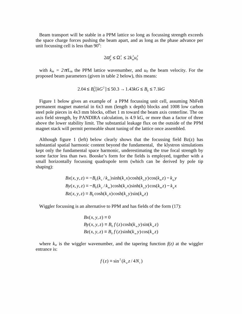
Beam transport will be stable in a PPM lattice so long as focussing strength exceedsthe space charge forces pushing the beam apart, and as long as the phase advance perunit focussing cell is less than 90o:
20
222 22 0 ukmp ≤Ω≤ω
with km = 2π/Lm the PPM lattice wavenumber, and u0 the beam velocity. For theproposed beam parameters (given in table 2 below), this means:
kGBkGkGB 1.743.13.50][04.2 022
0 ≤≤→≤≤
Figure 1 below gives an example of a PPM focussing unit cell, assuming NbFeBpermanent magnet material in 6x3 mm (length x depth) blocks and 1008 low carbonsteel pole pieces in 4x3 mm blocks, offset 1 m toward the beam axis centerline. The onaxis field strength, by PANDIRA calculation, is 4.9 kG, or more than a factor of threeabove the lower stability limit. The substantial leakage flux on the outside of the PPMmagnet stack will permit permeable shunt tuning of the lattice once assembled.
Although figure 1 (left) below clearly shows that the focussing field Bz(z) hassubstantial spatial harmonic content beyond the fundamental, the klystron simulationskept only the fundamental space harmonic, underestimating the true focal strength bysome factor less than two. Booske’s form for the fields is employed, together with asmall horizontally focussing quadrupole term (which can be derived by pole tipshaping):
)sin()cosh()cosh(),,(
)cos()sinh()cosh()/(),,(
)cos()cosh()sinh()/(),,(
0
0
0
zkykxkBzyxBz
xkzkykxkkkBzyxBy
ykzkykxkkkBzyxBx
myx
qmyxmy
qmyxmx
=
−−=
−−=
Wiggler focussing is an alternative to PPM and has fields of the form (17):
)cos()sinh()(),,(
)sin()cosh()(),,(
0),,(
0
0
zkykzfBzyxBz
zkykzfBzyxBy
zyxBx
ww
ww
===
where kw is the wiggler wavenumber, and the tapering function f(z) at the wigglerentrance is:
)4/(sin)( 2tw Nzkzf =

with Nt counting the length of the taper in wiggler periods. As with the PPMfocussing, astute pole tip shaping can be used effectively to provide force balance inboth horizontal and vertical planes.
FIGURE 1. PPM cell fields for 16 mm period length (left) and wiggler cell fields for 8 mm period length(right). Plotted fields are well above the stability threshold fields in each case, indicating that meeting thestability requirement is straightforward.
For Wiggler focussing to be stable, the same force balance condition must be met aswith the PPM lattice, but owing to the different spatial wavenumber controlling thevertical focussing (it is kw=2π/Lw, which scales like the wiggle period length, ratherthan ky, which scales like the vertical PPM magnet dimension), the condition is (18):
wwp BkG <→Ω< 0.12
γω
for the present case, with eww meB /=Ω . As with the PPM focussing, the basic
focussing mechanism is pondermotive: the beam is pushed towards the point ofminimum magnetic field energy density by a force proportional to the gradient in |B|2.For the PPM focussing the variation was fast, scaling with the vertical height of thePCM magnet gap. For the wiggler focussing, the fields vary much more slowly in thevertical plane, allowing a much larger matched vertical beam size. Figure 1 above(right) shows the magnetic field strength for a wiggler focussing cell with an 8 mm celllength.

Additional beam area convergence is possible by appropriate tapering of the entrancefields of the transport lattice. By adding a matching telescope (a quadrupole doublet)near the start of the focussing lattice, it is possible to further reduce the vertical beamsize by a useful amount, easing the cathode current density loading. Figure 2 belowshows both analytic (left) and 3D PIC simulation (right) of 4:1 vertical compressionand subsequent match to a wiggler lattice.
FIGURE 2. Envelope integration (left) and 3D PIC simulation (right) of compressed, taper matched,wiggler focussed sheet beam showing 4:1 vertical compression
Klystron Waveguide Cavity Design
The conventional modes used for klystron cavities, the TM010 mode of the cylindricalpillbox, and its Cartesian analog, the TM110 mode of the rectangular pillbox, both haveelectric fields which vary rather rapidly off the cavity axis. This would give rise touneven bunching of a sheet beam, and make impossible a uniform impedance matchbetween beam and output cavity for maximum efficiency. Alternative cavity geometriesmust therefore be considered.
Several high aspect ratio cavity geometries have been proposed for the SBK. (19) Thecandidate considered here is a variant of the “barbell” cavity proposed by Miller(20). Itis simply a section of slotted waveguide operating in the TE10 mode just above cutoff,hence βz §(]GRHVQRWYDU\DORQJWKHJXLGHOHQJWKDQGWKHJXLGHLPSHGDQFHLVYHU\high. The cutoff waveguide is terminated in a λ/4 waveguide section at each end tomatch between the high impedance cutoff waveguide and the shorting plane at thecoupling aperture. In practice the matching cavities at each end are somewhat shorterthan λ/4 due to the coupling aperture in the outer wall.
A cold test model of a non-reentrant slotted waveguide cavity was built at X-band totest the field flatness and electrical properties of the proposed geometry. The R/Q

profile was deduced by resonant perturbation methods, using a dielectric rod insertedthough the cavity beam tube and is shown in figure 3 below.
FIGURE 3. Non-reentrant 20:1 X-band waveguide cavity cold test model, showing cutoff waveguidesection (left) [beam opening faces upward], λ/4 cavity and coupling iris (center), capacitive field probe(top center) and waveguide (right), and measured R/Q of model.
With a low R/Q, design of an efficient output circuit becomes more difficult,requiring travelling wave output structure to raise the shunt impedance high enough togive good coupling to the beam. Efforts to improve the R/Q of the structure wereclearly indicated.
A simple extension of the barbell cavity involves substituting a slotted, ridgedwaveguide for the slotted rectangular guide of the barbell cavity. By making the cavityre-entrant in this fashion, it becomes possible to dimension the cavity and gapindependently, allowing gap coupling constant considerations to set the gap length, andcavity Q and R/Q considerations to dimension the cavity proper. The ridged waveguide,like the rectangular waveguide, must be operated close to cutoff to give good fieldflatness, but this is not difficult, owing to the large slot cut for the beam tube, whichtends to compensate the increase in capacitance from the reentrancy. The addition of re-entrant “noses” to the structure is a complication which changes only the cutoffwaveguide cross section profile, and thus is not significantly more difficult to fabricate.
The computed field profile Ez(x,y) for a 20:1 aspect ratio re-entrant waveguide cavityis shown in figure 4 below.
FIGURE 4. Contour plot of Ez(x,y); the beam motion is into the page.

Parameters of this 20:1 cavity are summarized in table 1 below. The R/Q of thewaveguide cavity varies inversely with the aspect ratio of the “flat-field” region,
TABLE 1. Reentrant 20:1 aspect ratio cavity properties.Parameter Value
Frequency, TM110
Nearest mode TM310
Mode Separation (∆f*Qo/fo)Qo
R/QR/Q/Aspect Ratio
91.392 GHz95.5579 GHz>50117219.4 Ω388 Ω/20:1
TM210 cannot couple to sourceTM310-TM110
See text)RU [ \ SDUWLFOH
implying that a 40:1 cavity would have approximately half the R/Q value of the 20:1cavity shown. Consequently, the invariant quantity “R/Q/´GHILQHGDVWKHSURGXFWRIthe aspect ratio and the R/Q, is also given below as a more generally applicable figureof merit.
The main virtue of the SBK is that the beam current may be increased beyond theround beam value without increasing the beam perveance and lowering the tubeefficiency. Thus, the wider the beam, the more output power may be obtained. Severalpractical constraints must be considered which impose a limit to the beam width.
One limit on the length of the cutoff waveguide section of the barbell cavity isimposed by mode competition from the adjacent cavity modes, which grow closer asthe cutoff section grows longer:
LxLx
n
Lx
mkkk nm
1∝−=−≡∆ ππ
Clearly as the horizontal length Lx becomes greater, the separation between TMn10
modes decreases. A practical length limit is therefore determined by the requirementthat the TM110 and TM210 modes be separated by at least the twice the sum of theirrespective 3dB loaded bandwidths (200-500), requiring:
≈≤of
QcLx
233 cm
A far stricter limitation comes from the requirement of field flatness in the cutoffwaveguide. Impedance tapering the cutoff waveguide section(21) is one possible wayto relax this constraint.

Oscillation/Mode Leakage Issues
The drift spaces between the cavities for the SBK have dimensions that permit theTEn0 modes to propagate at the klystron operating frequency. For the chosen 20:1aspect ratio, the first six modes, TE10 through TE60, all are above cutoff at the klystronoperating frequency. Although none of these modes is capable of being driven by asymmetric TM110 cavity mode, imperfections of the real klystron cavities will causesome coupling to each of these modes. Common to all the TE modes are substantialwall currents flowing in the narrow wall of the waveguide. Consequently, slotting thedrift tube on the narrow walls, and mounting of an RF absorber such as SiC or lossyceramic in the slots will suppress these modes, and is the solution adopted here. Yu andWilson(20) proposed and numerically demonstrated that choke cavities couldeffectively suppress the communicating modes of the drift tubes on a mode-by-modebasis, but this scheme requires the addition of another set of cavities to the klystronthat must be tuned, and is quite mode-specific, whereas slotting the drift tube wallsdamps all modes with appreciable wall currents in the vicinity.
Additional damping can be provided by lining the top and bottom surfaces of the drifttube with lossy conducting material, which will further increase the attenuation of thedrift tube modes.
KLYSTRON SIMULATION
Small-signal analytic treatment using a MathCAD program developed by SLAC forround beam klystrons and modified for sheet beam klystrons was used to establishrough values for optimal cavity Q, frequency and placement for the chosen beam aspectratio, voltage and current.
Optimal cavity performance was tuned up using the 3D finite difference EM solverGdfidL, solved again (in Magic3D) in the time domain by Green function techniques toestablish the “hot” cavity properties, and then coded into a Magic3D simulation of theklystron, beginning from the focal waist after the electron gun. Detailed parameters forthe design prototype are shown in table 2 below.
A proof-of-principle numerical experiment to test the possibility of extractingsignificant RF power from a sheet beam in a waveguide output cavity was carried out.A 15A, 140 kV sheet beam was imprinted with an ideal amplitude RF currentmodulation, then allowed to interact with a waveguide cavity. The cavity was loadedwith lossy material at the position of the coupling apertures, to achieve the samegeneral field shape and Q as could be expected from a waveguide-coupled cavity. Thekinetic energy as a function of z and the power extracted (i.e. the power loss in the a

Table 2. Target parameters for sheet beam klystron design.Parameter Value CommentsCenter frequencyBandwidth# CavitiesSmall-signal GainBeam VoltageBeam CurrentPerveanceBeam DimensionsPerveance per SquareBeam PowerCurrent DensityCathode Current DensityGun Compression RatioMatching Comp. RatioConfining field PeakPCM Lattice wavelengthPlasma WavelengthCavity R/QDrift Tube Dimensions
91.392 GHz70 MHz325 dB140 kV15 A0.29 µP0.4 x 8 mm14.4 nP/2.25 MW469 A/cm2
4.69 A/cm2
25:14:11550 G8 mm75 mm19.4 Ω0.6 x 10.0 mm
32xSLAC1 dB BW
150 kV max
20:1 aspect ratio
100:1 convergenceWiggler + 0.05 T/m HF quadrupole
Re-entrant geometry
aperture load) are shown in figure 5 below. A power extraction efficiency of 35% wasobserved in the best case, providing evidence that efficient power extraction from asheet beam is possible with the proposed waveguide cavity geometry.
FIGURE 5. Ideally bunched beam interacting with a loaded waveguide cavity. Kinetic energy asa function of propagation distance (left) and ohmic power loss in one of two aperture loads as afunction of time. The true output power would be twice the value shown.

FIGURE 6. Geometry of 3-cavity sheet beam klystron for the Magic3D simulations.
As can be seen in figure 6, several measures have been taken to curb oscillations,both real, and numerical in origin. The drift tubes have been slotted and an idealabsorber inserted in the gap to dampen the TE modes. The top and bottom surfaces ofthe drift tubes have been loaded with lossy material to dampen higher-order TM modeswhich would be otherwise excited by numerical noise. The drift space beyond theoutput cavity has likewise been loaded with an ideal RF absorber to catch the initialplane wave launched when the electron beam is turned on, and to provide furtherdampening for the drift tube modes.
Cavity Qs are set by the conductance of the lossy material within each cavity, and bythe size of the coupling aperture (input and output cavities only). Coupling aperturedimensions are set by observing the gap voltage, wall loss power, and drive power(through the waveguide) to the cavity, and inferring the respective Qs from aknowledge of the cavity R/Q.
Drive power to the input is established by enforcing a normalization on a linespanning the input waveguide parallel to the guide electric field.

Electrons are emitted starting at what would be the beam waist following the electrongun for the klystron and transported in a wiggler lattice to a conducting walldownstream of the output cavity. Properties of the focussing optics are given in table 3below.
TABLE 3. Wiggler focussing parameters.Parameter ValueWiggler Period 8 mmNumber of periods 6Taper length 2 periodsOn-Axis Induction 1150 GaussPole Gap (vertical) 1.5 mmBackground Quad horizontally focussingBack. Quad gradient 10 T/m
The difficulties involved in constructing a full 3D simulation of the RF circuit for theSBK are such that at this time only a poorly optimized klystron example can be given.Figure 7 below shows the small-signal (see, for example (21)) performances for boththe optimized 3-cavity klystron (which assumes an extended output circuit) and thepresent case, showing that there is substantial room for improvement. The largestimprovement will come from incorporating the extended output circuit, correcting theerrant cavity Qs and coupling βs, and adjusting the wiggler focussing to give more evenbeam transport.
FIGURE 7. Optimal, and current simulation expected performances for the 3-cavity sheet beamklystron.
Figure 8 below shows the beam bunching in the horizontal and vertical planes, withthe vertical focussing effects of the barbell cavity plainly visible. The overfocussing inthe vertical plane occurs for much lower (factor of 4) wiggler field strength than oneexpects by straightforward integration of the beam envelope equations (22), providing

evidence that the vertical space charge fields are inadequately represented in thesimulation.
FIGURE 8. Beam bunching for the 3-cavity SBK in the horizontal (top) and vertical (bottom) planes.
Power input and output, as measured at a plane (different from the port plane) in theentrance and exit waveguides, respectively, is shown in figure 9 below. Twowaveguides connect to each of the input and output cavities, so the actual power valuesare twice those shown.
FIGURE 9. Input and output power to 3-cavity SBK. Actual input and output powers are twicethose shown. Data shown required 4 days of computation time to produce.

The output power of 17.5kW versus 370W input gives a power gain of only 16.7 dB,and a negligible power efficiency. But as shown in the cavity tuning table below, thereis clearly room for improvement. Cavity parameter values for the simulation arededuced from power dissipations, gap voltages and the cavity’s computed R/Q.
TABLE 4. Cavity parameters for 3-cavity SBK, both optimized case (in a smallsignal sense) and the Magic3D simulated case.
ParameterOptimized
fo[GHz]
Qo Qe R/Q[Ω]
drift[mm]
InputIdlerOutputSimulatedInputIdlerOutput
91.39291.40591.39291.4191.4691.41
1200120012002590162882502
40083510501090
202090 20 20 20
24241818
The bunching shown in figure 10 below is computed by integrating the currentdensity across a plane perpendicular to the axis of the klystron, in a manner reflectiveof how the beam would interact with a waveguide cavity at that point. Any curving ofthe space charge waves due to the wiggler focussing, space charge effects ornonuniformity of the RF fields in the upstream cavities would reduce the observed RFcurrent component.
FIGURE 10. Bunching harmonic amplitudes 2 mm upstream of the output cavity.
The dominant reason for the poor efficiency of the simulation klystron is thesubstantial mismatch between the output gap impedance and the beam impedance. Forthe given parameters, the output gap impedance should ideally be(25):

Ω=== k
I
IM
I
VQRQZ
dc
rfo
oegap 61
1)/(
2
whereas the simulation klystron gap impedance is Qe(R/Q) = 21 kΩ, too low by afactor of three. This low impedance causes the gap voltage to be too low to effectivelyextract the beam kinetic energy, and as is plainly visible in figure 8 above, the RFbunch structure remains relatively intact after the output cavity.
FUTURE DIRECTIONS
Several areas remain to be covered. The electron gun design, although consistent withelectron guns that have been or are currently operating(17,18,24,26), must beaddressed. The possibility of tailoring the beam impedance to vary commensuratelywith the gap impedance of the cavities must also be addressed, and the complexitiesinvolved weighed against the elaborate output cavity coupling schemes required tomaintain a high degree of field flatness. Once decided, the multi-cell, travelling orstanding wave output structure must be designed.
Issues of klystron stability against charge density fluctuations and structuremisalignment must be addressed to establish alignment tolerances on the RF cavitiesrelative to the drift tubes. Simulations indicate that charge centroid asymmetries(equivalent to a net displacement of the cavity off the klystron centerline) on of order 1micron do not induce oscillation. Studies of beam-asymmetry induced coupling tohigher modes of the cavity will also have to be examined closely.
More exotic issues to address include the design of the quasi-optical outputcombining optics for adding together the output of several SBKs to achieve the powerlevels desired, and the possibility of performing the output power combination inconcert with binary pulse compression to produce short, high power pulses.
CONCLUSIONS
A fully three-dimensional simulation incorporating the beam transport, cavity, andpower in/out coupling schemes in a manner consistent with a realizable tube has beenpresented. Although the gain and efficiency for the particular case shown are less thanexciting, the causes of the poor performance are understood, and easily remedied.Given the long simulation running times (days), the Magic3D model is clearly ananalysis tool rather than a synthesis tool, but provides the demonstrated ability to modelthe performance of a sheet beam klystron in full three-dimensional detail.
The three major physics issues unique to the sheet beam klystron, those of beam edgeerosion, poor beam cavity coupling, and drift tube oscillations have been brought undercontrol under the fairly ideal circumstances presented here. Thorough numerical
modeling studies under less ideal circumstances will indicate whether more aggressivemeasures, such as the inclusion of choke cavities(23) in the drift tubes [to suppressoscillations], are necessary.
ACKNOWLEDGEMENTS
The authors gratefully acknowledge many illuminating discussions with RogerMiller, Daryl Sprehn, Glenn Scheitrum, Robert Siemann, David Whittum, and PerryWilson.
REFERENCES
1. P. B. Wilson, AIP Conf. Proc. 397, 191 (1997).2. R. H. Siemann, “Advanced Electron Linacs”, in Proc. Symp. Elec. Lin. Accel.,Stanford, CA, SLAC-R-526, (1998).3. D. H. Whittum, “Switched Matrix Accelerator”, ARDB-86, (1997).4. G. Caryotakis, “Development of X-band Klystron Technology at SLAC”, in Proc. ofthe Part. Accel. Conf., Vancouver, B.C., (1997).5. D. N. Smithe, M. Bettenhausen, L. Ludeking, “3-D Simulations of Multiple BeamKlystrons”, in these proceedings (1998).6. E. P. Eppley, SLAC Memorandum dated July 1, 1986.7. D. U. L. Yu, J. S. Kim, P. B. Wilson, “Design of a High-Power Sheet BeamKlystron”, in Proc. IEEE Part. Accel. Conf., Washington D.C., March 16-19, (1997).8. K. R. Eppley, W. B. Hermannsfeldt, R. H. Miller, “Design of a Wiggler-Focussed,Sheet Beam X Band Klystron”, in Proc. of the IEEE Part. Accel. Conf., Washington D.C., March 16-19, (1997).9. H. H. Meinel, “Commercial Applications of Millimeterwaves: History, PresentStatus, and Future trends”, IEEE MTT, 43, (7), p. 1639-53, (1995).10. S. V. Robertson, G. M. Rebeiz, “Micromachined W-Band Filters”, IEEE MTT, 44,(4), p. 598-606, (1996).11. D. Rutledge, “Micro-machining in Submillimeter-Wave Circuits”, IEEE MTT-SDigest, p. 1889-92, (1996).12. W. R. Fowkes, “Cavity Resonator Measurements at 90 GHz”, ARDB-164, (1997).13. D. T. Palmer, to be published in Proc. Adv. Accel. Conc. Conf., Baltimore, MD,(1998).14. J. Song, “Deep X-ray Lithography Fabrication of MM-Wave Cavities at theAdvanced Photon Source”, in Proc. of XIXth LINAC Conf., Chicago, IL, (1998).15. R. Merte, R. Apel, “S-parameter Measurement of W-band Muffin-tin WBAND-003”, TET-NOTE 98/06, (1998).16. J. H. Booske, B. D. McVey, T.M. Antonsen, “Stability and Confinement ofNonrelativistic Sheet Electron Beams with Periodic Cusped Magnetic Focusing”, J.Appl. Phys., 73, (9), p. 4140-55, (1993).

17. Z. Zhang, et al, “Experimental and Numerical Studies of Sheet Electron BeamPropagation through a Planar Wiggler Magnet”, IEEE Tran. Plasma Sci., 21, (6), p.760-7, (1993).18. J. H. Booske, et al, “Propagation of Wiggler Focussed Relativistic Sheet ElectronBeams”, J. Appl. Phys., 64, (1), p. 6-11, (1988).19. S. Solyga, “Two-Dimensional Design of a Low-Voltage mm-Wave Sheet BeamKlystron”, TET-NOTE 98/01, (1998).20. R. Miller, private communication, (1998).21. K. H. Kreuchen, A. A. Auld, N. E. Dixon, “A Study of the Broadband FrequencyResponse of the Multicavity Klystron Amplifier”, J. Elect., p 529-67, (1957).22. P. Lapostolle, “Proton Linear Accelerators: A Theoretical and Tistoricalintroduction”, LA-11601-MS, (1989).23. D. Yu, P. B. Wilson, “Sheet-Beam Klystron RF Cavities”, in Proc. IEEE Part.Accel. Conf, Washington, D. C., p 2681-3, (1993).24. D. J. Radack, J. H. Booske, Y. Carmel, W. W. Destler, “Wiggler FocussedRelativistic Sheet Beam Propagation in a Planar Free-Electron Laser Configuration”,Appl .Phys. Lett., 55, (20), p. 2069-71, (1989).25. G. Caryotakis, “The Klystron: A Microwave Source of Surprising Range andEndurance”, SLAC-PUB-7731, (1998).26. V. L. Granatstein, et al, “Near-Millimeter Free Electron Lasers with Small periodWigglers and Sheet Electron Beams”, NIM, A272, p.110-16, (1988).