VSX-609RDS - Njord Noatun's Vintage Audio · PDF file2 VSX-709RDS, VSX-609RDS 1. SAFETY...
64
ORDER NO. PIONEER CORPORATION 4-1, Meguro 1-chome, Meguro-ku, Tokyo 153-8654, Japan PIONEER ELECTRONICS SERVICE, INC. P.O. Box 1760, Long Beach, CA 90801-1760, U.S.A. PIONEER EUROPE N.V. Haven 1087, Keetberglaan 1, 9120 Melsele, Belgium PIONEER ELECTRONICS ASIACENTRE PTE. LTD. 253 Alexandra Road, #04-01, Singapore 159936 PIONEER CORPORATION 2000 c RRV2274 1. SAFETY INFORMATION ...................................... 2 2. EXPLODED VIEWS AND PARTS LIST ............... 3 3. BLOCK DIAGRAM AND SCHEMATIC DIAGRAM ..... 8 4. PCB CONNECTION DIAGRAM ......................... 28 5. PCB PARTS LIST ............................................... 43 6. ADJUSTMENT .................................................... 48 CONTENTS 7. GENERAL INFORMATION ................................ 49 7.1 DISASSEMBLY ............................................ 49 7.2 PARTS .......................................................... 50 7.2.1 IC ............................................................ 50 7.2.2 DISPLAY ................................................. 55 8. PANEL FACILITIES AND SPECIFICATIONS ....... 57 T – ZZK MAR. 2000 Printed in Japan THIS MANUAL IS APPLICABLE TO THE FOLLOWING MODEL(S) AND TYPE(S). AUDIO/VIDEO MULTI-CHANNEL RECEIVER VSX-709RDS VSX-609RDS Type Model Power Requirement Remarks VSX-709RDS VSX-609RDS MYXJIEW AC220-230V MYXJIGR AC220-230V MVXJI AC230V
Transcript of VSX-609RDS - Njord Noatun's Vintage Audio · PDF file2 VSX-709RDS, VSX-609RDS 1. SAFETY...
ORDER NO.
PIONEER CORPORATION 4-1, Meguro 1-chome, Meguro-ku, Tokyo 153-8654, JapanPIONEER ELECTRONICS SERVICE, INC. P.O. Box 1760, Long Beach, CA 90801-1760, U.S.A.PIONEER EUROPE N.V. Haven 1087, Keetberglaan 1, 9120 Melsele, BelgiumPIONEER ELECTRONICS ASIACENTRE PTE. LTD. 253 Alexandra Road, #04-01, Singapore 159936 PIONEER CORPORATION 2000c
RRV2274
1. SAFETY INFORMATION...................................... 2
2. EXPLODED VIEWS AND PARTS LIST ............... 3
3. BLOCK DIAGRAM AND SCHEMATIC DIAGRAM..... 8
4. PCB CONNECTION DIAGRAM ......................... 28
5. PCB PARTS LIST ............................................... 43
6. ADJUSTMENT .................................................... 48
CONTENTS7. GENERAL INFORMATION ................................ 49
7.1 DISASSEMBLY ............................................ 49
7.2 PARTS .......................................................... 50
7.2.1 IC ............................................................ 50
7.2.2 DISPLAY ................................................. 55
8. PANEL FACILITIES AND SPECIFICATIONS....... 57
T – ZZK MAR. 2000 Printed in Japan
THIS MANUAL IS APPLICABLE TO THE FOLLOWING MODEL(S) AND TYPE(S).
AUDIO/VIDEO MULTI-CHANNEL RECEIVER
VSX-709RDSVSX-609RDS
TypeModel
Power Requirement RemarksVSX-709RDS VSX-609RDS
MYXJIEW AC220-230V
MYXJIGR AC220-230V
MVXJI AC230V
2
VSX-709RDS, VSX-609RDS
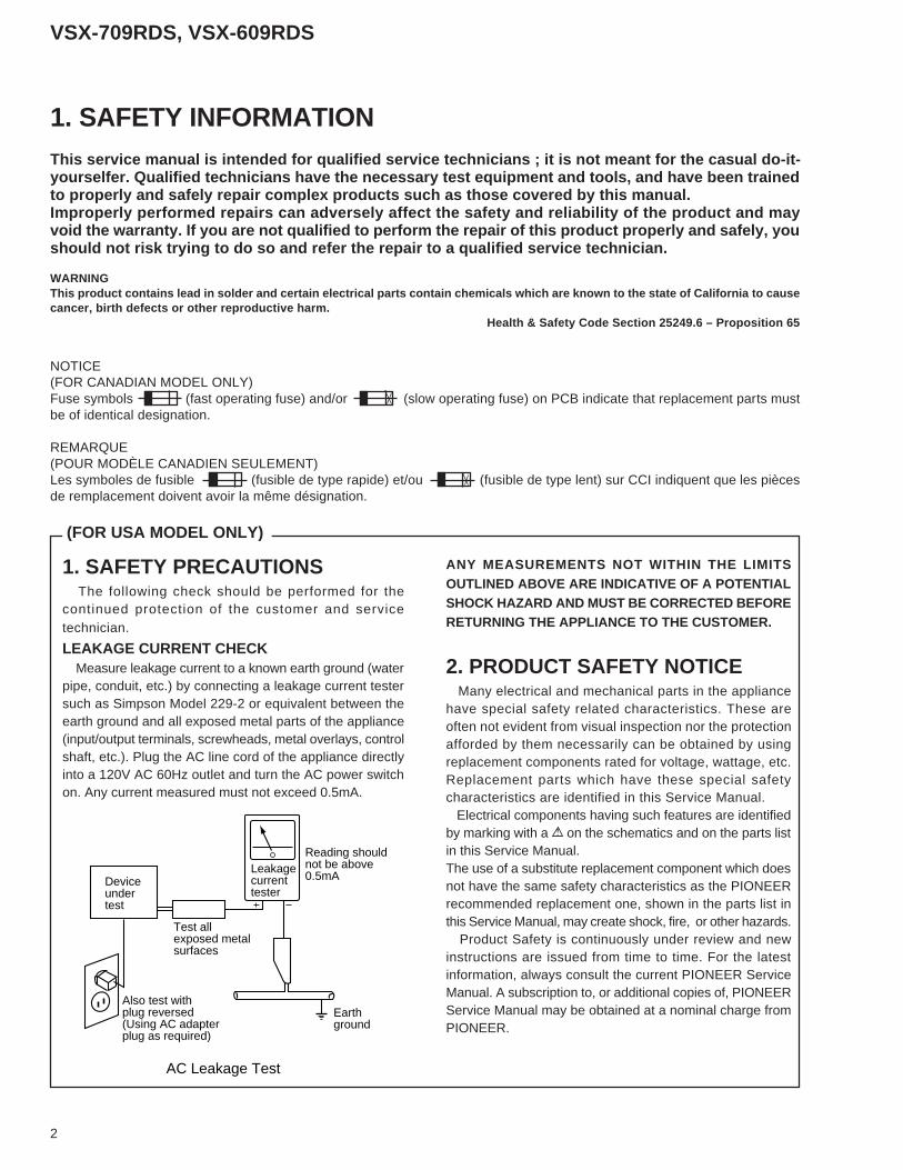
1. SAFETY INFORMATIONThis service manual is intended for qualified service technicians ; it is not meant for the casual do-it-yourselfer. Qualified technicians have the necessary test equipment and tools, and have been trainedto properly and safely repair complex products such as those covered by this manual.Improperly performed repairs can adversely affect the safety and reliability of the product and mayvoid the warranty. If you are not qualified to perform the repair of this product properly and safely, youshould not risk trying to do so and refer the repair to a qualified service technician.
WARNINGThis product contains lead in solder and certain electrical parts contain chemicals which are known to the state of California to causecancer, birth defects or other reproductive harm.
Health & Safety Code Section 25249.6 – Proposition 65
NOTICE(FOR CANADIAN MODEL ONLY)Fuse symbols (fast operating fuse) and/or (slow operating fuse) on PCB indicate that replacement parts mustbe of identical designation.
REMARQUE(POUR MODÈLE CANADIEN SEULEMENT)Les symboles de fusible (fusible de type rapide) et/ou (fusible de type lent) sur CCI indiquent que les piècesde remplacement doivent avoir la même désignation.
ANY MEASUREMENTS NOT WITHIN THE LIMITSOUTLINED ABOVE ARE INDICATIVE OF A POTENTIALSHOCK HAZARD AND MUST BE CORRECTED BEFORERETURNING THE APPLIANCE TO THE CUSTOMER.
2. PRODUCT SAFETY NOTICE Many electrical and mechanical parts in the appliancehave special safety related characteristics. These areoften not evident from visual inspection nor the protectionafforded by them necessarily can be obtained by usingreplacement components rated for voltage, wattage, etc.Replacement parts which have these special safetycharacteristics are identified in this Service Manual. Electrical components having such features are identifiedby marking with a on the schematics and on the parts listin this Service Manual.The use of a substitute replacement component which doesnot have the same safety characteristics as the PIONEERrecommended replacement one, shown in the parts list inthis Service Manual, may create shock, fire, or other hazards. Product Safety is continuously under review and newinstructions are issued from time to time. For the latestinformation, always consult the current PIONEER ServiceManual. A subscription to, or additional copies of, PIONEERService Manual may be obtained at a nominal charge fromPIONEER.
1. SAFETY PRECAUTIONS The following check should be performed for thecontinued protection of the customer and servicetechnician.
LEAKAGE CURRENT CHECK Measure leakage current to a known earth ground (waterpipe, conduit, etc.) by connecting a leakage current testersuch as Simpson Model 229-2 or equivalent between theearth ground and all exposed metal parts of the appliance(input/output terminals, screwheads, metal overlays, controlshaft, etc.). Plug the AC line cord of the appliance directlyinto a 120V AC 60Hz outlet and turn the AC power switchon. Any current measured must not exceed 0.5mA.
(FOR USA MODEL ONLY)
Leakagecurrenttester
Reading shouldnot be above0.5mADevice
undertest
Test allexposed metalsurfaces
Also test withplug reversed(Using AC adapterplug as required)
Earthground
AC Leakage Test
3
VSX-709RDS, VSX-609RDS
1
2
4
73
8
9
5
17
10
11
6
5
6
12
MYXJIEW andMVXJI Types Only
VSX-709RDS Only
VSX-609RDS
13
MYXJIEW andMYXJIGR Types Only
MYXJIEW Type Only
1516
14
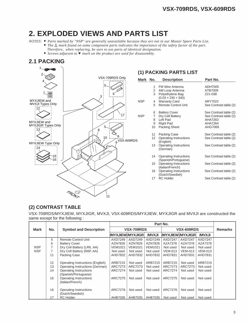
2.1 PACKING
1 FM Wire Antenna ADH70052 AM Loop Antenna ATB70093 Polyethylene Bag Z21-038
(0.03 × 230 × 340)NSP 4 Warranty Card ARY7022
5 Remote Control Unit See Contrast table (2)
6 Battery Cover See Contrast table (2)NSP 7 Dry Cell Battery See Contrast table (2)
8 Left Pad AHA72639 Right Pad AHA7264
10 Packing Sheet AHG7069
11 Packing Case See Contrast table (2)12 Operating Instructions See Contrast table (2)
(English)13 Operating Instructions See Contrast table (2)
(German)
14 Operating Instructions See Contrast table (2)(Spanish/Portuguese)
15 Operating Instructions See Contrast table (2)(Italian/French)
16 Operating Instructions See Contrast table (2)(Dutch/Swedish)
17 RC Holder See Contrast table (2)
(1) PACKING PARTS LISTMark No. Description Part No.
2. EXPLODED VIEWS AND PARTS LISTNOTES: • Parts marked by "NSP" are generally unavailable because they are not in our Master Spare Parts List.
• The mark found on some component parts indicates the importance of the safety factor of the part. Therefore, when replacing, be sure to use parts of identical designation.
• Screws adjacent to mark on the product are used for disassembly.
(2) CONTRAST TABLEVSX-709RDS/MYXJIEW, MYXJIGR, MVXJI, VSX-609RDS/MYXJIEW, MYXJIGR and MVXJI are constructed thesame except for the following :
Part No.
Mark No. Symbol and Description VSX-709RDS VSX-609RDS Remarks
/MYXJIEW /MYXJIGR /MVXJI /MYXJIEW /MYXJIGR /MVXJI5 Remote Control Unit AXD7249 AXD7249 AXD7249 AXD7247 AXD7247 AXD72476 Battery Cover AZN7826 AZN7826 AZN7826 AZA7378 AZA7378 AZA7378
NSP 7 Dry Cell Battery (LR6, AA) VEM1021 VEM1021 VEM1021 Not used Not used Not usedNSP 7 Dry Cell Battery (R6P, AA) Not used Not used Not used VEM-013 VEM-013 VEM-013
11 Packing Case AHD7832 AHD7832 AHD7832 AHD7831 AHD7831 AHD7831
12 Operating Instructions (English) ARB7215 Not used ARB7215 ARB7215 Not used ARB721513 Operating Instructions (German) ARC7273 ARC7273 Not used ARC7273 ARC7273 Not used14 Operating Instructions ARC7274 Not used Not used ARC7274 Not used Not used
(Spanish/Portuguese)15 Operating Instructions ARC7275 Not used Not used ARC7275 Not used Not used
(Italian/French)
16 Operating Instructions ARC7276 Not used Not used ARC7276 Not used Not used(Dutch/Swedish)
17 RC Holder AHB7035 AHB7035 AHB7035 Not used Not used Not used

4
VSX-709RDS, VSX-609RDS
G
D
L
K
H
M
J
I
CI
J
MLK
H
E
E
B
A
CD
F
N
N
F
A
B
35
45
46
G
36
31
18
24
19
36
3636
36
3636
36
36
36
3636
36
36
36
26
15
7
12
5
27
12
13
14
16
36
4344
36
17
4
3
9 8
6
36
11
36
36
37
3738
3836
3636
10
Accessory ofFront Panel
36
34
36
36
47
36
Refer to"2.3 FRONT PANEL SECTION".
39
39
29
28
30
41
42
47
36
31
23
36
For MVXJI Type
20
21
19
36
39
36
3625
39
39
33
33
22
VSX-709RDS Only
2.2 EXTERIOR SECTION
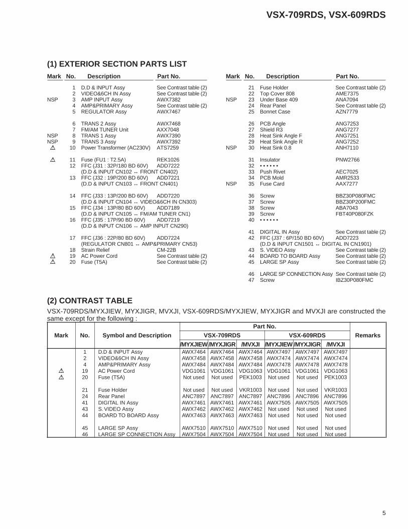
5
VSX-709RDS, VSX-609RDS
1 D.D & INPUT Assy See Contrast table (2)2 VIDEO&6CH IN Assy See Contrast table (2)
NSP 3 AMP INPUT Assy AWX73824 AMP&PRIMARY Assy See Contrast table (2)5 REGULATOR Assy AWX7467
6 TRANS 2 Assy AWX74687 FM/AM TUNER Unit AXX7048
NSP 8 TRANS 1 Assy AWX7390NSP 9 TRANS 3 Assy AWX7392 10 Power Transformer (AC230V) ATS7259
11 Fuse (FU1 : T2.5A) REK102612 FFC (J31 : 32P/180 BD 60V) ADD7222
(D.D & INPUT CN102 ↔ FRONT CN402)13 FFC (J32 : 19P/200 BD 60V) ADD7221
(D.D & INPUT CN103 ↔ FRONT CN401)
14 FFC (J33 : 13P/200 BD 60V) ADD7220(D.D & INPUT CN104 ↔ VIDEO&6CH IN CN303)
15 FFC (J34 : 13P/80 BD 60V) ADD7189(D.D & INPUT CN105 ↔ FM/AM TUNER CN1)
16 FFC (J35 : 17P/90 BD 60V) ADD7219(D.D & INPUT CN106 ↔ AMP INPUT CN290)
17 FFC (J36 : 22P/80 BD 60V) ADD7224(REGULATOR CN801 ↔ AMP&PRIMARY CN53)
18 Strain Relief CM-22B 19 AC Power Cord See Contrast table (2) 20 Fuse (T5A) See Contrast table (2)
(1) EXTERIOR SECTION PARTS LISTMark No. Description Part No. Mark No. Description Part No.
21 Fuse Holder See Contrast table (2)22 Top Cover 808 AME7375
NSP 23 Under Base 409 ANA709424 Rear Panel See Contrast table (2)25 Bonnet Case AZN7779
26 PCB Angle ANG725327 Shield R3 ANG727728 Heat Sink Angle F ANG725129 Heat Sink Angle R ANG7252
NSP 30 Heat Sink 0.8 ANH7110
31 Insulator PNW276632 • • • • • •33 Push Rivet AEC702534 PCB Mold AMR2533
NSP 35 Fuse Card AAX7277
36 Screw BBZ30P080FMC37 Screw BBZ30P200FMC38 Screw ABA704339 Screw FBT40P080FZK40 • • • • • •
41 DIGITAL IN Assy See Contrast table (2)42 FFC (J37 : 6P/150 BD 60V) ADD7223
(D.D & INPUT CN1501 ↔ DIGITAL IN CN1901)43 S. VIDEO Assy See Contrast table (2)44 BOARD TO BOARD Assy See Contrast table (2)45 LARGE SP Assy See Contrast table (2)
46 LARGE SP CONNECTION Assy See Contrast table (2)47 Screw IBZ30P080FMC
(2) CONTRAST TABLEVSX-709RDS/MYXJIEW, MYXJIGR, MVXJI, VSX-609RDS/MYXJIEW, MYXJIGR and MVXJI are constructed thesame except for the following :
Part No.
Mark No. Symbol and Description VSX-709RDS VSX-609RDS Remarks
/MYXJIEW /MYXJIGR /MVXJI /MYXJIEW /MYXJIGR /MVXJI1 D.D & INPUT Assy AWX7464 AWX7464 AWX7464 AWX7497 AWX7497 AWX74972 VIDEO&6CH IN Assy AWX7458 AWX7458 AWX7458 AWX7474 AWX7474 AWX74744 AMP&PRIMARY Assy AWX7484 AWX7484 AWX7484 AWX7478 AWX7478 AWX747819 AC Power Cord VDG1061 VDG1061 VDG1063 VDG1061 VDG1061 VDG106320 Fuse (T5A) Not used Not used PEK1003 Not used Not used PEK1003
21 Fuse Holder Not used Not used VKR1003 Not used Not used VKR100324 Rear Panel ANC7897 ANC7897 ANC7897 ANC7896 ANC7896 ANC789641 DIGITAL IN Assy AWX7461 AWX7461 AWX7461 AWX7505 AWX7505 AWX750543 S. VIDEO Assy AWX7462 AWX7462 AWX7462 Not used Not used Not used44 BOARD TO BOARD Assy AWX7463 AWX7463 AWX7463 Not used Not used Not used
45 LARGE SP Assy AWX7510 AWX7510 AWX7510 Not used Not used Not used46 LARGE SP CONNECTION Assy AWX7504 AWX7504 AWX7504 Not used Not used Not used
6
VSX-709RDS, VSX-609RDS
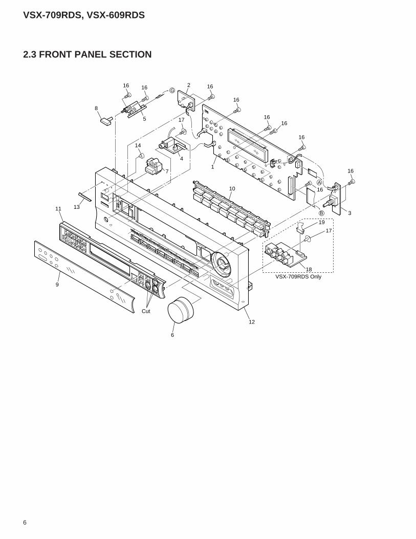
2.3 FRONT PANEL SECTION
G
B
A
11 13
10
14
17
7
4
2
6
Cut
9
12
18
17
1
3
16
16
1616
16
16
16
19
16
8
5
16
VSX-709RDS Only

7
VSX-709RDS, VSX-609RDS
(1) FRONT PANEL SECTION PARTS LIST
Mark No. Description Part No.
1 FRONT Assy See Contrast table (2)2 POWER SW Assy AWX7385
NSP 3 R. ENCODER Assy AWX7386NSP 4 H.P. Assy AWX7556
5 MECHA SW Assy AWX7443
6 Volume Knob AAB71797 Power Button AAD74408 Power Button M AAD74429 Window AAK7721
10 F Button See Contrast table (2)
Mark No. Description Part No.
11 Sub Panel AAD755212 F Panel See Contrast table (2)13 Name Plate PAM177614 LED Lens PNW201915 • • • • • •
16 Screw PPZ30P080FMC17 Screw ABA700918 FRONT VIDEO Assy See Contrast table (2)19 8P Shield Cable See Contrast table (2)
(2) CONTRAST TABLEVSX-709RDS/MYXJIEW, MYXJIGR, MVXJI, VSX-609RDS/MYXJIEW, MYXJIGR and MVXJI are constructed thesame except for the following :
Part No.
Mark No. Symbol and Description VSX-709RDS VSX-609RDS Remarks
/MYXJIEW /MYXJIGR /MVXJI /MYXJIEW /MYXJIGR /MVXJI1 FRONT Assy AWX7459 AWX7459 AWX7459 AWX7477 AWX7477 AWX747710 F Button AAD7564 AAD7564 AAD7564 AAD7562 AAD7562 AAD756212 F Panel AMB7677 AMB7677 AMB7677 AMB7675 AMB7675 AMB767518 FRONT VIDEO Assy AWX7460 AWX7460 AWX7460 Not used Not used Not used19 8P Shield Cable ADX7306 ADX7306 ADX7306 Not used Not used Not used
VSX-709RDS, VSX-609RDS
8
A
B
C
D
1 2 3 4
1 2 3 4
N
P
7
5
9
3
1
11
CN901
3
CN354
IC351, IC352
3
P3
CN901
4
CN301
8
8
P CN901
6
CN107
3
5
FRONT VIDEO ASSY
S. VIDEO ASSY
FRONT VIDEO ASSY
FRONT VIDEO ASSY
AXX7048UNIT
CN105
6
CN305
IC101
IC303
IC1901
IC302
IC302
IC301
IC104
IC102
IC1701IC1101
IC1201
B
H
J
77
7
1 9
11
CN1047
9
11
CN1901
2
CN1501
2
5
3
7
5
9
1
11
5
5
3
2 5
1
3
4
6
123
38
38
21
26
2325
6 7
IC17036 7
IC1705
DTS DECODER
6 7
IC17051 2
4
6
3
8
7
19
1817
1211
10
9
5
1
7
2
11
9 10
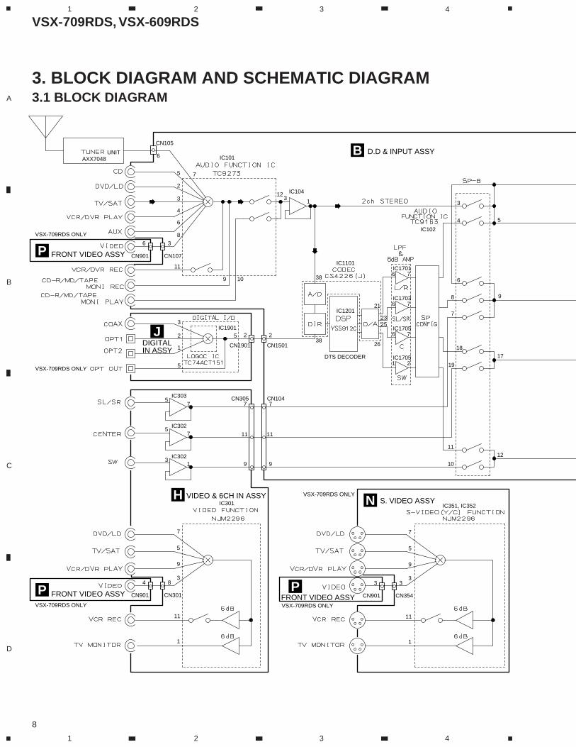
D.D & INPUT ASSY
DIGITAL IN ASSY
VIDEO & 6CH IN ASSY
VSX-709RDS ONLY
VSX-709RDS ONLY
VSX-709RDS ONLY VSX-709RDS ONLY
VSX-709RDS ONLY
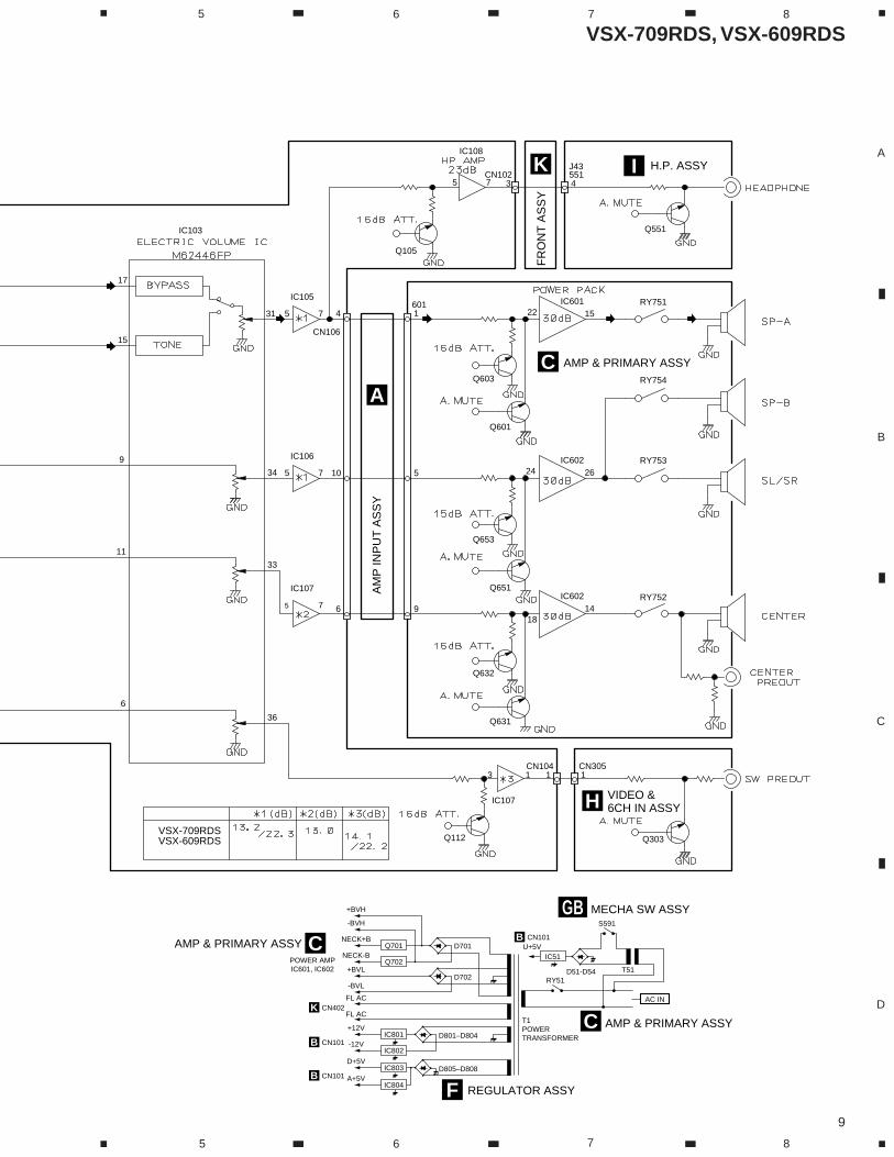
3. BLOCK DIAGRAM AND SCHEMATIC DIAGRAM3.1 BLOCK DIAGRAM
VSX-709RDS, VSX-609RDS
9
A
B
C
D
5 6 7 8
5 6 7 8
IC103
IC105
IC106
IC107
IC108
IC107
Q112 Q303
Q603
Q601
Q653
Q651
Q632
Q631
H
CN1041
CN3051
11
15
17
31
34
33
36
6
9
5 7
5 7
5 7
5 7
3 1
IC602
1814
IC60224 26
IC601 RY751
RY753
RY754
RY752
22 15
Q551
Q105
IK
C
A
CN1023
551J43
4
CN106
46011
10 5
6 9
+12V
-12V
T1POWERTRANSFORMER
T51
AC IN
D801–D804
U+5V
D51-D54RY51
IC51
IC801CN101
IC802
NECK+B
POWER AMPIC601, IC602
NECK-B
D702
D701
+BVL
+BVH
-BVH
-BVL
FL AC
FL AC
Q701
Q702
S591
C
CB
D+5VD805–D808IC803
A+5VIC804
CN101
FB
CN101B
CN402K
AMP & PRIMARY ASSY
GB MECHA SW ASSY
AMP & PRIMARY ASSY
REGULATOR ASSY
AMP & PRIMARY ASSY
VIDEO & 6CH IN ASSY
H.P. ASSY
FR
ON
T A
SS
Y
AM
P IN
PU
T A
SS
Y
VSX-709RDSVSX-609RDS
VSX-709RDS, VSX-609RDS
10
A
B
C
D
1 2 3 4
1 2 3 4
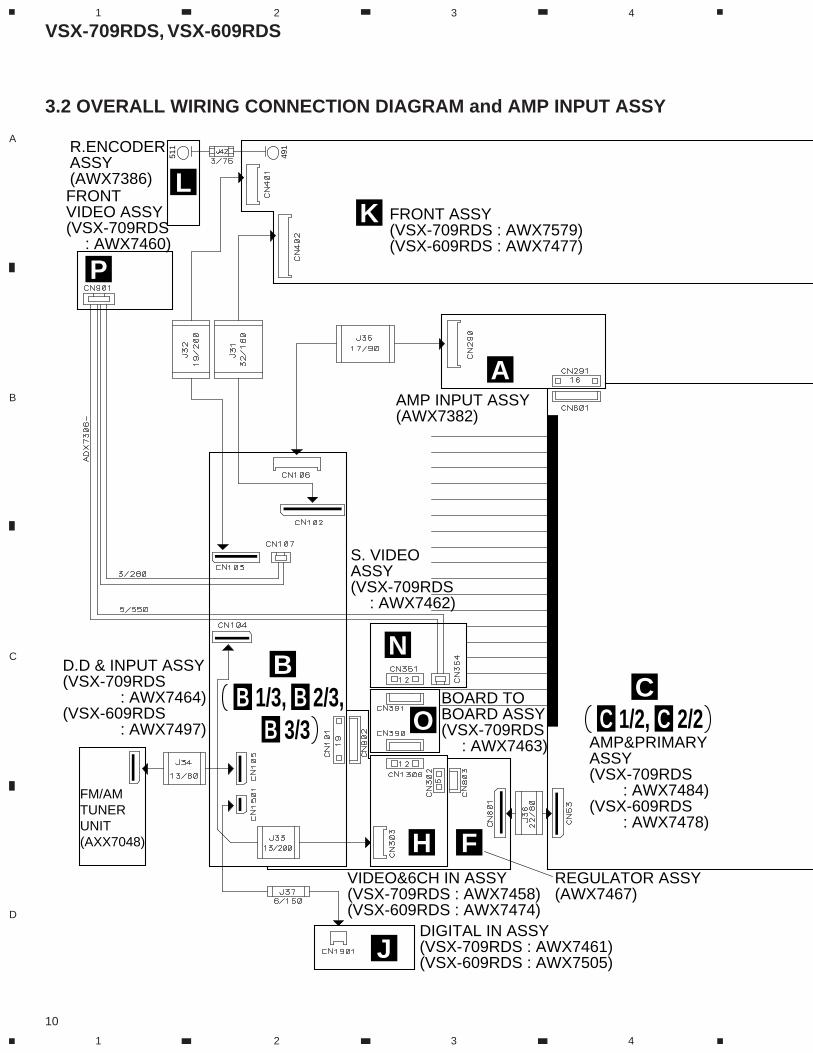
3.2 OVERALL WIRING CONNECTION DIAGRAM and AMP INPUT ASSY
BOARD TOBOARD ASSY(VSX-709RDS
: AWX7463)
S. VIDEOASSY(VSX-709RDS
: AWX7462)
FRONT VIDEO ASSY(VSX-709RDS
: AWX7460)
N
P
O
FRONT ASSY(VSX-709RDS : AWX7579)(VSX-609RDS : AWX7477)
K
R.ENCODER ASSY(AWX7386) L
D.D & INPUT ASSY(VSX-709RDS
: AWX7464)(VSX-609RDS
: AWX7497)
B
REGULATOR ASSY(AWX7467)
F
DIGITAL IN ASSY(VSX-709RDS : AWX7461)(VSX-609RDS : AWX7505)
J
VIDEO&6CH IN ASSY(VSX-709RDS : AWX7458)(VSX-609RDS : AWX7474)
H
AMP&PRIMARY ASSY(VSX-709RDS
: AWX7484)(VSX-609RDS
: AWX7478)
C
AMP INPUT ASSY(AWX7382)
A
FM/AM TUNER UNIT(AXX7048)
491
511
C 1/2, C 2/2B 1/3, B 2/3,
B 3/3

VSX-709RDS, VSX-609RDS
11
A
B
C
D
5 6 7 8
5 6 7 8
Note : When ordering service parts, be sure to refer to "EXPLODED VIEWS and PARTS LIST" or "PCB PARTS LIST".
A
LARGE SP ASSY(VSX-709RDS : AWX7510)R
LARGE SP CONNECTION ASSY(VSX-709RDS : AWX7504)
Q
AMP INPUT ASSY (AWX7382)A
CN
106
CN
601
B1/3
C1/2
POWER SW ASSY(AWX7385)
M
H.P. ASSY(AWX7556)
I
TRANS3 ASSY(AWX7392)
E
TRANS1 ASSY(AWX7390)
GA
MECHA SW ASSY(AWX7443)
GB
TRANS2 ASSY(AWX7468)
D
471
J3
J7J6
501
403
551
701
851
J1J2
J4J5
VSX-709RDS, VSX-609RDS
12
A
B
C
D
1 2 3 4
1 2 3 4
VSX-709RDSVSX-609RDS
VSX-709RDS ONLY
VSX-709RDSVSX-609RDS
VSX-709RDS ONLY
CN
901
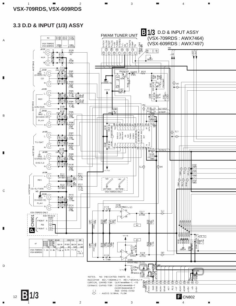
PD.D & INPUT ASSY
(VSX-709RDS : AWX7464)(VSX-609RDS : AWX7497)
B 1/3FM/AM TUNER UNIT
CN802F
3.3 D.D & INPUT (1/3) ASSY
1/3B
VSX-709RDS, VSX-609RDS
13
A
B
C
D
5 6 7 8
5 6 7 8
CN
290
AC
N40
1K
CN
402
K
B 3/3 B 2/3B 3/3
B 2/3B 3/3
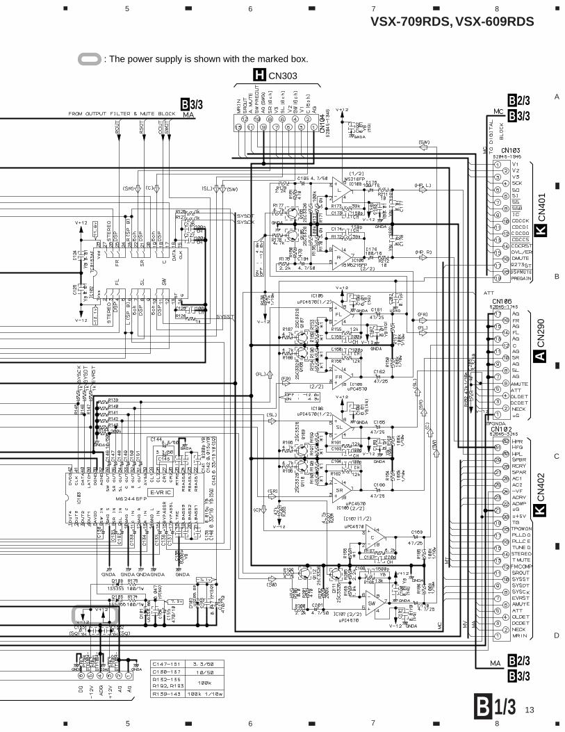
CN303H: The power supply is shown with the marked box.
E-VR IC
1/3B
VSX-709RDS, VSX-609RDS
14
A
B
C
D
1 2 3 4
1 2 3 4
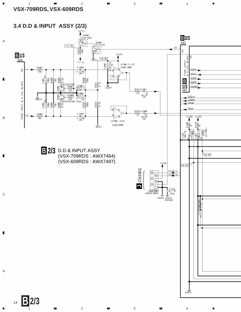
3.4 D.D & INPUT ASSY (2/3)
2/3B
D.D & INPUT ASSY(VSX-709RDS : AWX7464)(VSX-609RDS : AWX7497)
B 2/3
CN
1901
J
B 1/3
B 3/3
B1/3
VSX-709RDS, VSX-609RDS
15
A
B
C
D
5 6 7 8
5 6 7 8
2/3B
: The power supply is shown with the marked box.
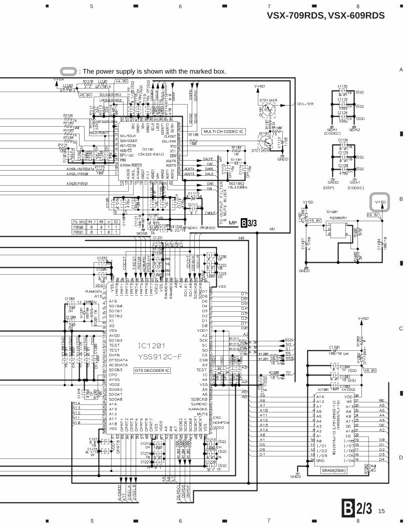
B 3/3
DTS DECODER IC
SRAM(256K)
MULTI CH CODEC IC
VSX-709RDS, VSX-609RDS
16
A
B
C
D
1 2 3 4
1 2 3 4
D.D & INPUT ASSY(VSX-709RDS : AWX7464)(VSX-609RDS : AWX7497)
B 3/3B 2/3
B 2/3 B 1/3
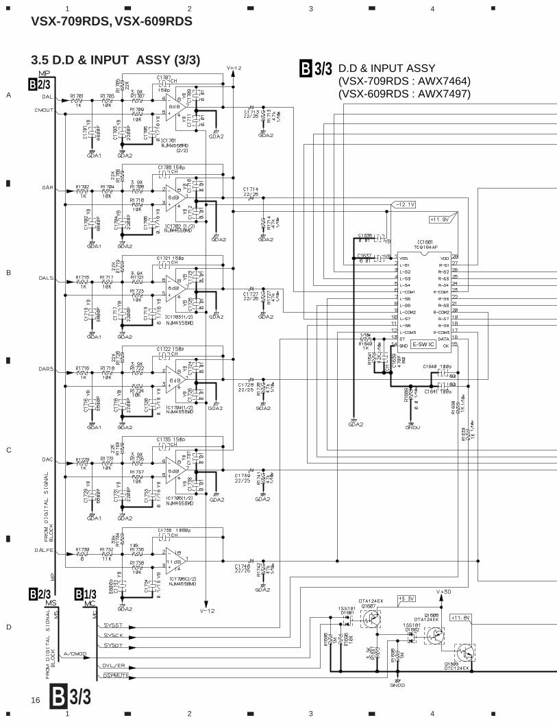
E-SW IC
3.5 D.D & INPUT ASSY (3/3)
3/3B
VSX-709RDS, VSX-609RDS
17
A
B
C
D
5 6 7 8
5 6 7 8
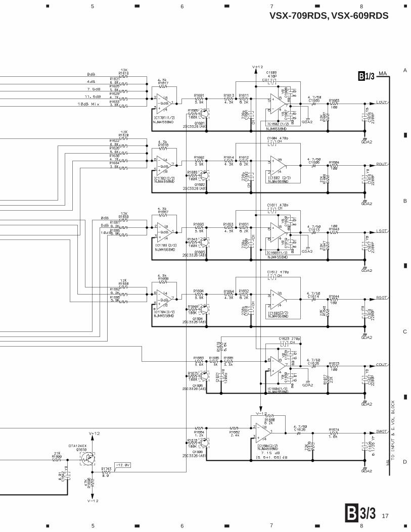
B 1/3
3/3B
VSX-709RDS, VSX-609RDS
18
A
B
C
D
1 2 3 4
1 2 3 4
12P12P
12P12P
12P12P
12P12P
12P12P
AMP&PRIMARY ASSY
(VSX-709RDS : AWX7484)(VSX-609RDS : AWX7478)C 1/2
CN
291
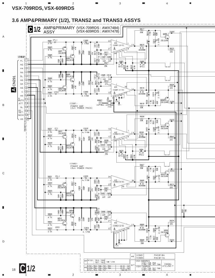
A3.6 AMP&PRIMARY (1/2), TRANS2 and TRANS3 ASSYS
1/2C

VSX-709RDS, VSX-609RDS
19
A
B
C
D
5 6 7 8
5 6 7 8
VSX-709RDSVSX-609RDS
VSX-709RDSVSX-609RDS
VSX-609RDS ONLY
VSX-709RDS ONLY
VSX-709RDS ONLY
TRANS3 ASSY(AWX7392)E
TRANS2 ASSY(AWX7468)
D
PO
WE
R T
RA
NS
FO
RM
ER
CN
785
Q
CAUTION : FOR CONTINUED PROTECTION AGAINST RISK OF FIRE.REPLACE ONLY WITH SAME TYPE NO. 49101.6 FOR IC851, IC852 AND IC853 MFD, BY LITTELFUSE INC.
CAUTION : FOR CONTINUED PROTECTION AGAINST RISK OF FIRE.REPLACE ONLY WITH SAME TYPE NO. 491001 FOR IC603 MFD, BY LITTELFUSE INC.
C 2/2
C 2/2
1/2C ED
VSX-709RDS, VSX-609RDS
20
A
B
C
D
1 2 3 4
1 2 3 4
2/2C
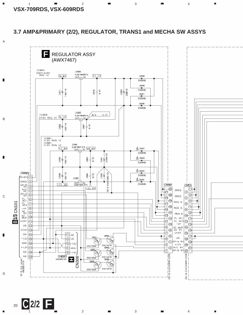
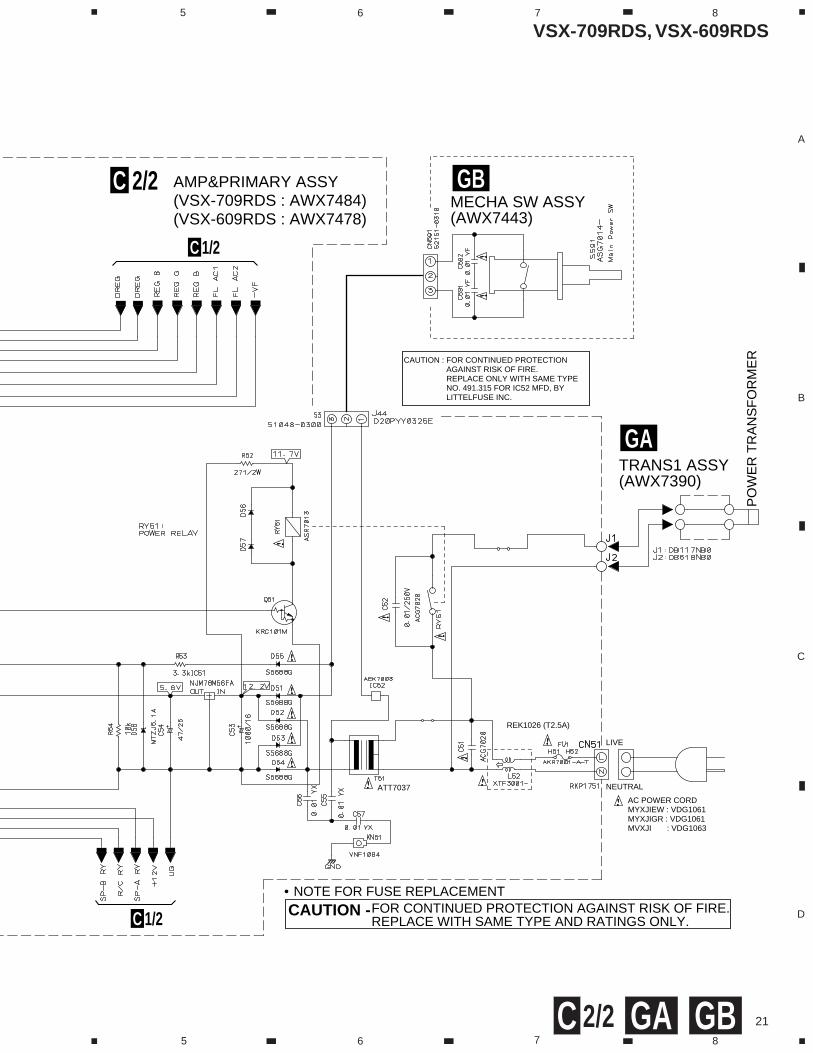
3.7 AMP&PRIMARY (2/2), REGULATOR, TRANS1 and MECHA SW ASSYS
F
CN
101
B1/3
REGULATOR ASSY(AWX7467)
F
CN
306
H
VSX-709RDS, VSX-609RDS
21
A
B
C
D
5 6 7 8
5 6 7 8
2/2C
AMP&PRIMARY ASSY(VSX-709RDS : AWX7484)(VSX-609RDS : AWX7478)
C 2/2
C 1/2
C 1/2
TRANS1 ASSY(AWX7390)
GB
GA
MECHA SW ASSY(AWX7443)
PO
WE
R T
RA
NS
FO
RM
ER
LIVE
NEUTRAL
REK1026 (T2.5A)
ATT7037
AC POWER CORDMYXJIEW : VDG1061MYXJIGR : VDG1061MVXJI : VDG1063
• NOTE FOR FUSE REPLACEMENTFOR CONTINUED PROTECTION AGAINST RISK OF FIRE.REPLACE WITH SAME TYPE AND RATINGS ONLY.
CAUTION -
CAUTION : FOR CONTINUED PROTECTION AGAINST RISK OF FIRE.REPLACE ONLY WITH SAME TYPE NO. 491.315 FOR IC52 MFD, BY LITTELFUSE INC.
GBGA
VSX-709RDS, VSX-609RDS
22
A
B
C
D
1 2 3 4
1 2 3 4
VSX-609RDS
VSX-709RDS
VSX-709RDS ONLY
CN
390
O
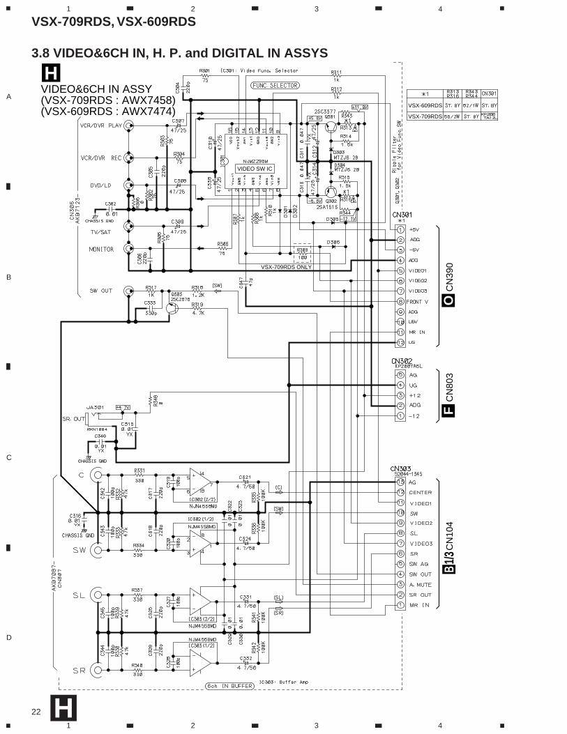
VIDEO&6CH IN ASSY(VSX-709RDS : AWX7458)(VSX-609RDS : AWX7474)
H
CN
104
CN
803
FB
1/3
VIDEO SW IC
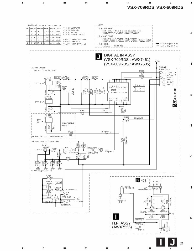
3.8 VIDEO&6CH IN, H. P. and DIGITAL IN ASSYS
H
VSX-709RDS, VSX-609RDS
23
A
B
C
D
1 2 3 4
1 2 3 4
VSX-709RDS ONLY
H.P. ASSY(AWX7556)
I
DIGITAL IN ASSY(VSX-709RDS : AWX7461)(VSX-609RDS : AWX7505)
J
CN
1501
B2/3
403K
JI
VSX-709RDS, VSX-609RDS
24
A
B
C
D
1 2 3 4
1 2 3 4
VSX-709RDS
VSX-609RDS
FRONT ASSY(VSX-709RDS : AWX7459)(VSX-609RDS : AWX7477)
KR.ENCODER ASSY(AWX7386)
L
CN
102
B1/3
CN
103
B1/3
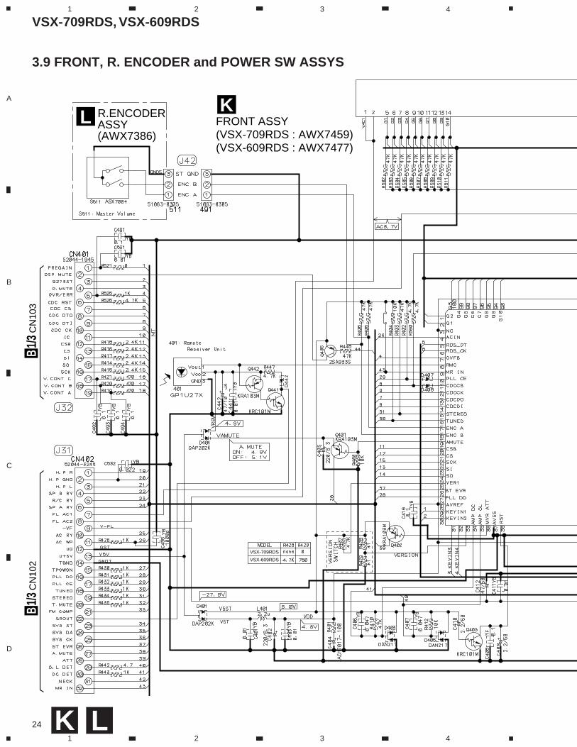
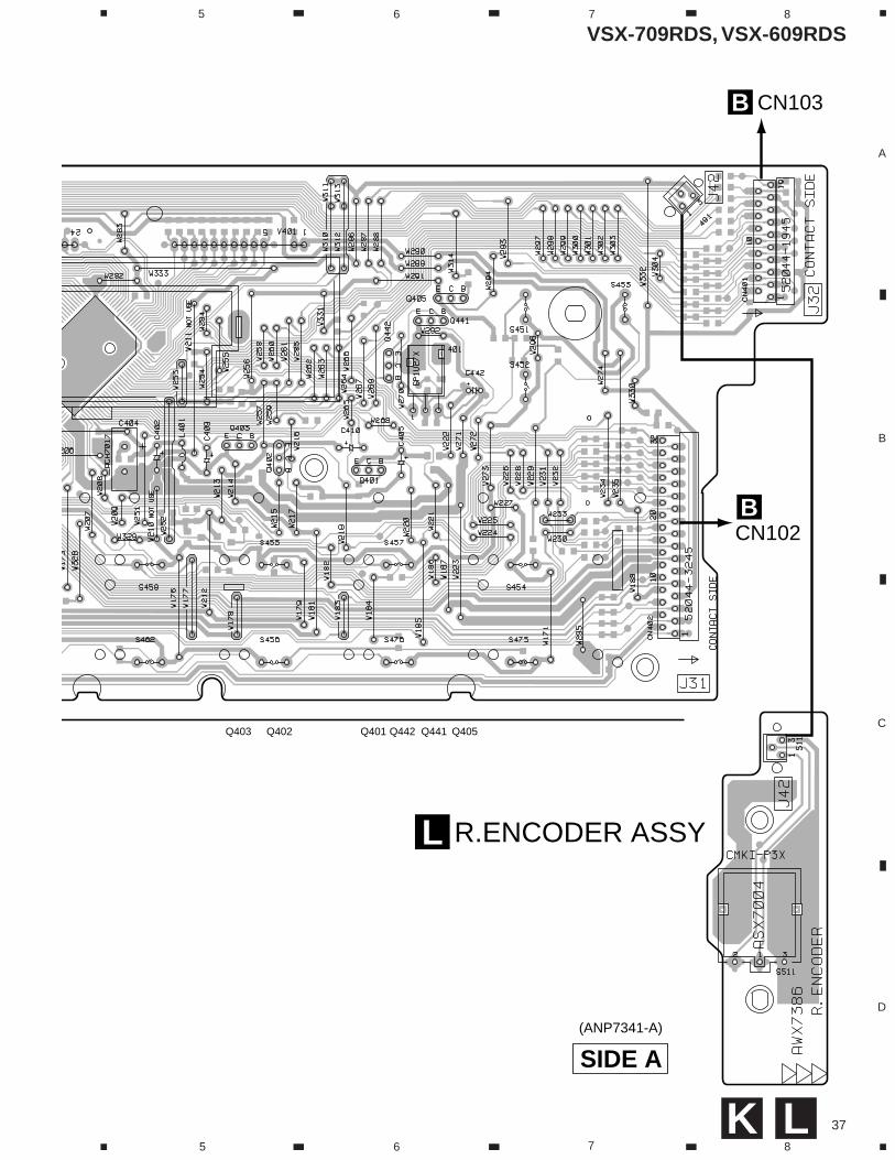
3.9 FRONT, R. ENCODER and POWER SW ASSYS
K L
VSX-709RDS, VSX-609RDS
25
A
B
C
D
5 6 7 8
5 6 7 8
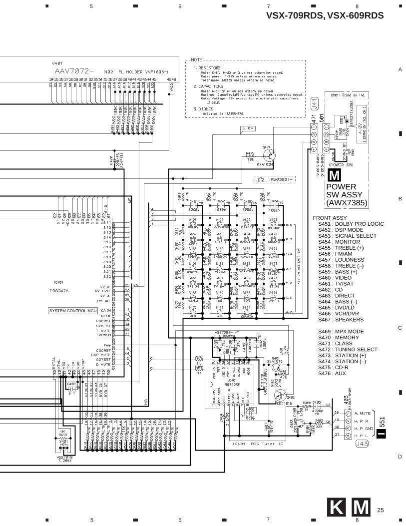
POWER SW ASSY(AWX7385)
M
551
I
FRONT ASSYS451 : DOLBY PRO LOGICS452 : DSP MODES453 : SIGNAL SELECTS454 : MONITORS455 : TREBLE (+)S456 : FM/AMS457 : LOUDNESSS458 : TREBLE (–)S459 : BASS (+)S460 : VIDEOS461 : TV/SATS462 : CDS463 : DIRECTS464 : BASS (–)S465 : DVD/LDS466 : VCR/DVRS467 : SPEAKERS
S469 : MPX MODES470 : MEMORYS471 : CLASSS472 : TUNING SELECTS473 : STATION (+)S474 : STATION (–)S475 : CD-RS476 : AUX
SYSTEM CONTROL MCU
MK
VSX-709RDS, VSX-609RDS
26
A
B
C
D
1 2 3 4
1 2 3 4
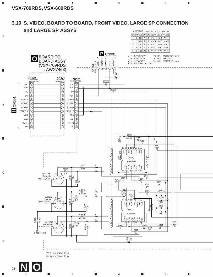
3.10 S. VIDEO, BOARD TO BOARD, FRONT VIDEO, LARGE SP CONNECTION
and LARGE SP ASSYS
N O
BOARD TO BOARD ASSY(VSX-709RDS
: AWX7463)
O
CN
301
H
CN901P
VSX-709RDS, VSX-609RDS
27
A
B
C
D
5 6 7 8
5 6 7 8RQ
LARGE SP CONNECTION ASSY(VSX-709RDS
: AWX7504)
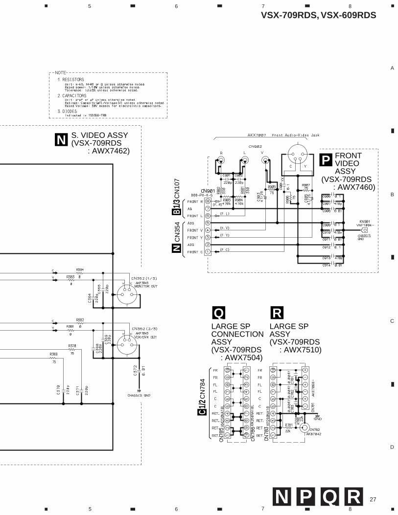
QLARGE SP ASSY(VSX-709RDS
: AWX7510)
R
FRONT VIDEOASSY
(VSX-709RDS : AWX7460)
P
S. VIDEO ASSY(VSX-709RDS
: AWX7462)N
CN
354
N
CN
784
C1/2
CN
107
B1/3
PN
VSX-709RDS, VSX-609RDS
28
A
B
C
D
1 2 3 4
1 2 3 4
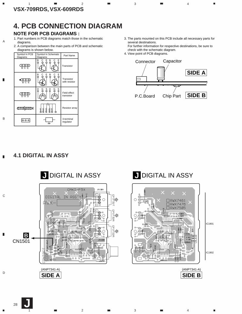
NOTE FOR PCB DIAGRAMS :1. Part numbers in PCB diagrams match those in the schematic diagrams.2. A comparison between the main parts of PCB and schematic diagrams is shown below.
3. The parts mounted on this PCB include all necessary parts for several destinations. For further information for respective destinations, be sure to check with the schematic diagram.4. View point of PCB diagrams.Symbol In PCB
DiagramsSymbol In SchematicDiagrams
Part Name
B C E
D
D
G
G
S
S
B C E
B C E
D G S
B C E B C E
B C E
Transistor
Transistorwith resistor
Field effecttransistor
Resistor array
3-terminalregulator
CapacitorConnector
P.C.Board Chip Part
SIDE A
SIDE B
4. PCB CONNECTION DIAGRAM
4.1 DIGITAL IN ASSY
J
(ANP7341-A)
CN1501B
SIDE A
DIGITAL IN ASSYJ
(ANP7341-A)
DIGITAL IN ASSYJ
SIDE B
IC1901
IC1902
VSX-709RDS, VSX-609RDS
29
A
B
C
D
1 2 3 4
1 2 3 4
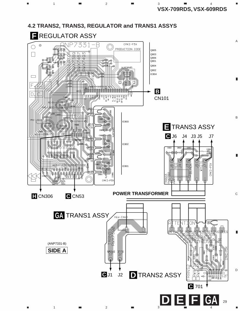
4.2 TRANS2, TRANS3, REGULATOR and TRANS1 ASSYS
FE
(ANP7331-B)
Q805
Q803
Q806Q801
Q804
Q802
IC804
REGULATOR ASSYF
TRANS3 ASSYE
TRANS2 ASSYD
CN53CCN306H
CN101B
701C
J1 J2C
J6 J4 J3 J5 J7C
SIDE A
IC802
IC803
IC801
POWER TRANSFORMER
TRANS1 ASSYGA
D GA
VSX-709RDS, VSX-609RDS
30
A
B
C
D
1 2 3 4
1 2 3 4
AMP INPUT ASSYA
AMP&PRIMARY ASSYC
CN106B
Q604Q606Q605Q602
Q603
IC601IC603
Q632
Q704Q702Q703
Q701
Q631
Q656
IC602
Q633
Q655
Q691
Q692
Q652Q654
Q651Q653
J7E
J6E
J3E
(ANP7331-B)
SIDE A
(ANP7331-B)
SIDE A
GB MECHA SW ASSY
(ANP7341-A)
SIDE B
(ANP7341-A)
SIDE A
A C
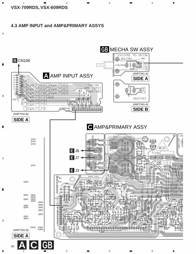
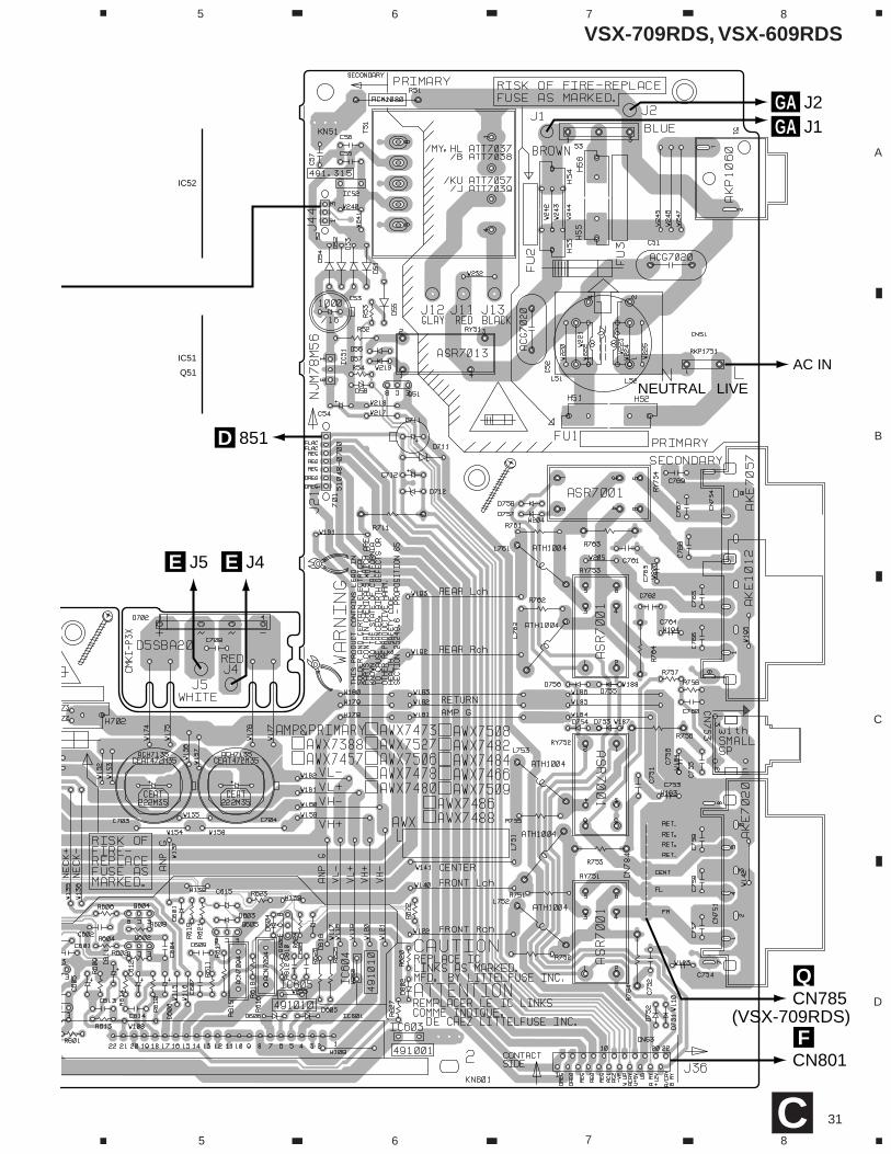
4.3 AMP INPUT and AMP&PRIMARY ASSYS
GB
VSX-709RDS, VSX-609RDS
31
A
B
C
D
5 6 7 8
5 6 7 8
J4EJ5E
851D
Q51
IC52
IC51 AC IN
NEUTRAL LIVE
CN801F
J2
GAGA
J1
CN785(VSX-709RDS)
Q
C
VSX-709RDS, VSX-609RDS
32
A
B
C
D
1 2 3 4
1 2 3 4B
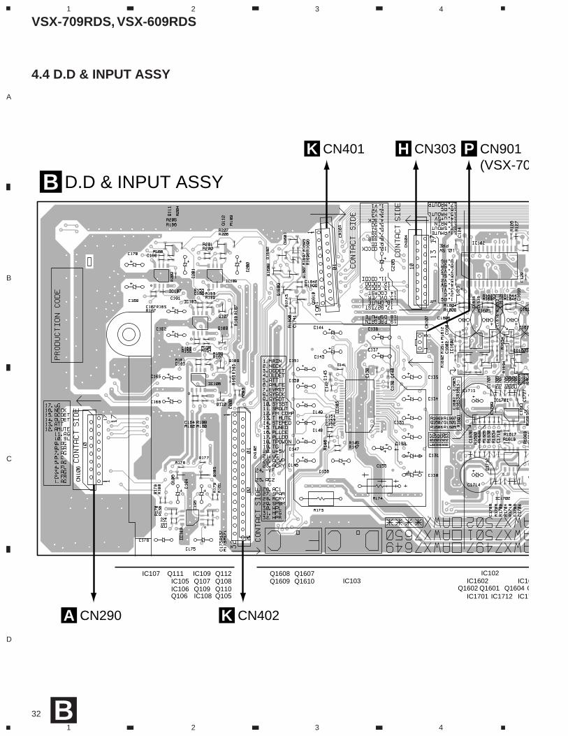
4.4 D.D & INPUT ASSY
D.D & INPUT ASSYB
CN402K
CN401K CN303H
CN290A
IC102IC1602IC103 IC16
IC1701 IC1712 IC17Q1602 Q1601 Q1604 Q
Q106
Q111IC107 Q112 Q1608 Q1607Q1609 Q1610Q107 Q108
Q109 Q110
IC109IC105IC106
IC108 Q105
CN901(VSX-70
P

VSX-709RDS, VSX-609RDS
33
A
B
C
D
5 6 7 8
5 6 7 8B
CN802F
CN1901J
IC1021602 IC1603 IC1604 IC1201
1701 IC1712 IC1704IC1703 IC1705 Q1003 Q1004 Q1001 Q1002
IC1101 IC1301Q101 Q102Q104 Q103
2 Q1601 Q1604 Q1603 Q1606 Q1605 IC1001IC104
IC1401Q1101 Q1102
(ANP7342-B)
SIDE A
FM/AM TUNER UNITCN901(VSX-709RDS)
VSX-709RDS, VSX-609RDS
34
A
B
C
D
1 2 3 4
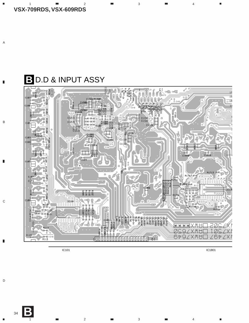
1 2 3 4B
D.D & INPUT ASSYB
IC1801IC101
VSX-709RDS, VSX-609RDS
35
A
B
C
D
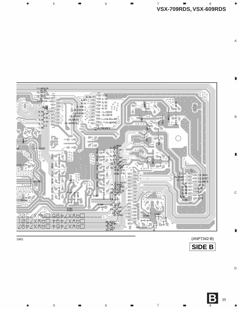
5 6 7 8
5 6 7 8B
C1801 (ANP7342-B)
SIDE B
VSX-709RDS, VSX-609RDS
36
A
B
C
D
1 2 3 4
1 2 3 4
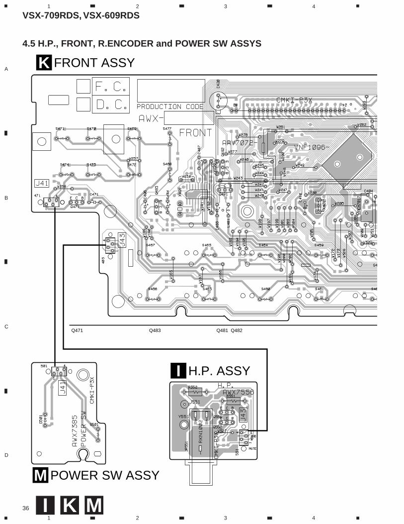
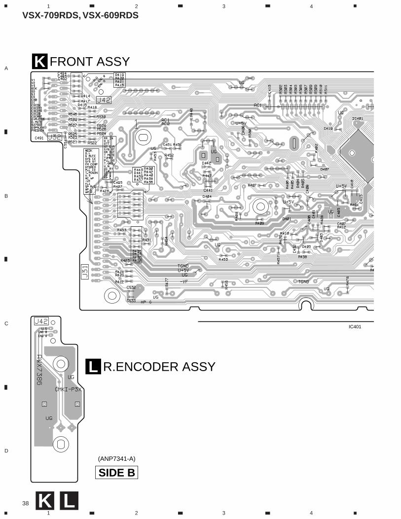
FRONT ASSYK
POWER SW ASSYM
H.P. ASSYI
Q471 Q483 Q481 Q482
4.5 H.P., FRONT, R.ENCODER and POWER SW ASSYS
I K M
VSX-709RDS, VSX-609RDS
37
A
B
C
D
5 6 7 8
5 6 7 8
LK
CN103B
CN102B
R.ENCODER ASSYL
Q441Q401 Q442 Q405Q402Q403
(ANP7341-A)
SIDE A
VSX-709RDS, VSX-609RDS
38
A
B
C
D
1 2 3 4
1 2 3 4K L
FRONT ASSYK
IC401
(ANP7341-A)
SIDE B
R.ENCODER ASSYL
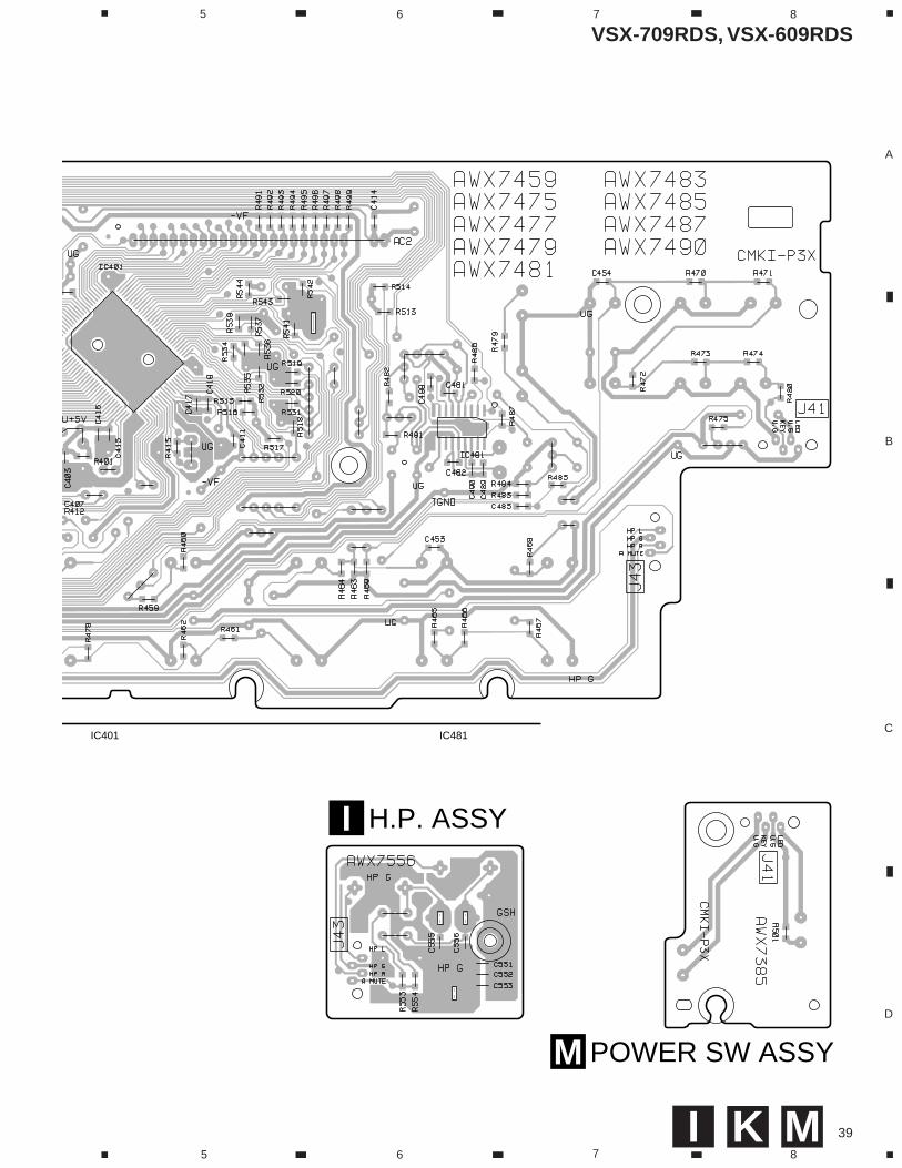
VSX-709RDS, VSX-609RDS
39
A
B
C
D
5 6 7 8
5 6 7 8MKI
IC481IC401
POWER SW ASSYM
H.P. ASSYI
VSX-709RDS, VSX-609RDS
40
A
B
C
D
1 2 3 4
1 2 3 4H
4.6 VIDEO&6CH IN ASSY
(ANP7341-A)
VIDEO&6CH IN ASSYH
CN104B
CN803F
SIDE A
Q301
Q303
Q306Q305
Q307Q304
Q302
(ANP7341-A)
SIDE B
VIDEO&6CH IN ASSYH
IC302
IC303
IC301
CN390O
(VSX-709RDS)
VSX-709RDS, VSX-609RDS
41
A
B
C
D
1 2 3 4
1 2 3 4
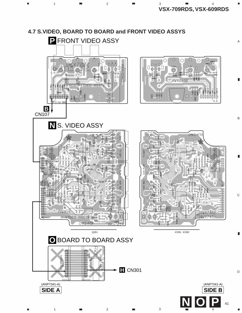
4.7 S.VIDEO, BOARD TO BOARD and FRONT VIDEO ASSYS
(ANP7341-A)
FRONT VIDEO ASSYP
CN107B
CN301H
SIDE A(ANP7341-A)
SIDE B
BOARD TO BOARD ASSYO
S. VIDEO ASSYN
IC351 IC352Q351
PON
VSX-709RDS, VSX-609RDS
42
A
B
C
D
1 2 3 4
1 2 3 4
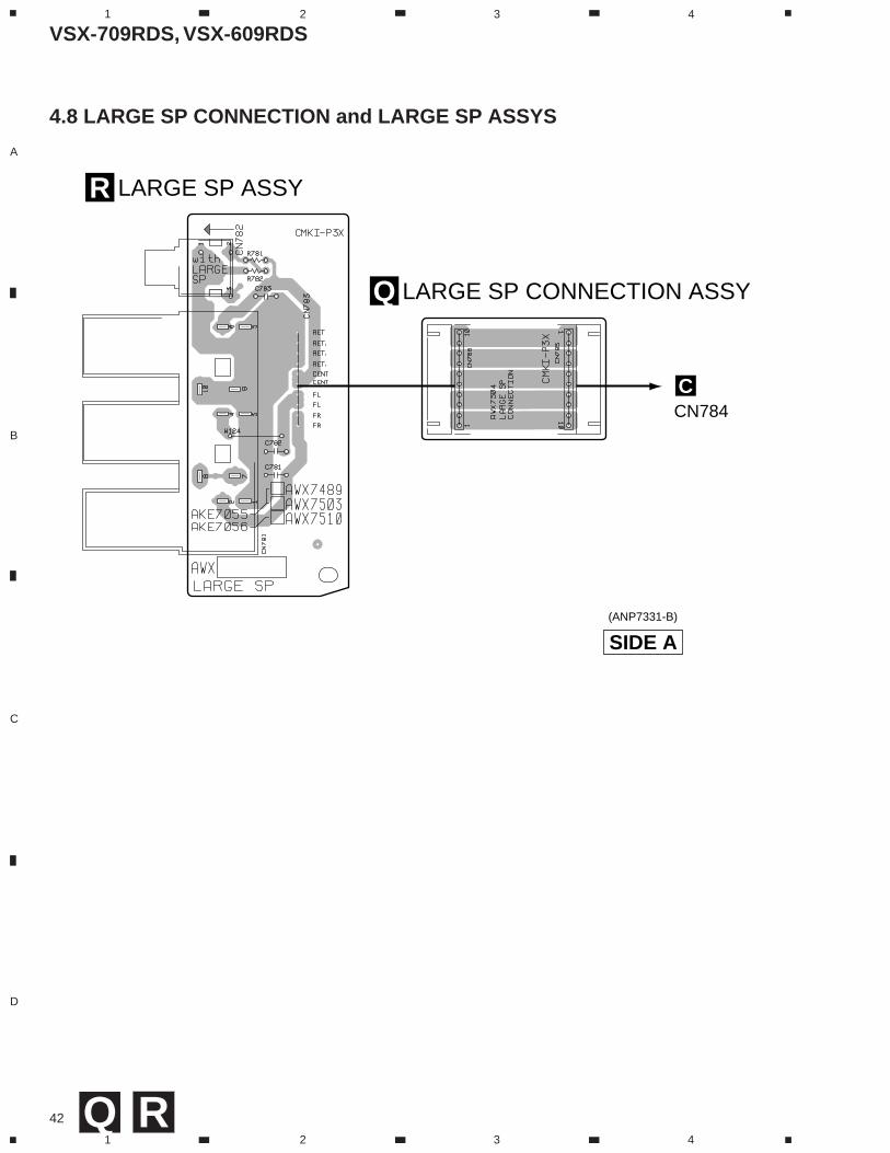
4.8 LARGE SP CONNECTION and LARGE SP ASSYS
Q R
(ANP7331-B)
LARGE SP ASSYR
LARGE SP CONNECTION ASSYQ
CN784C
SIDE A
43
VSX-709RDS, VSX-609RDS
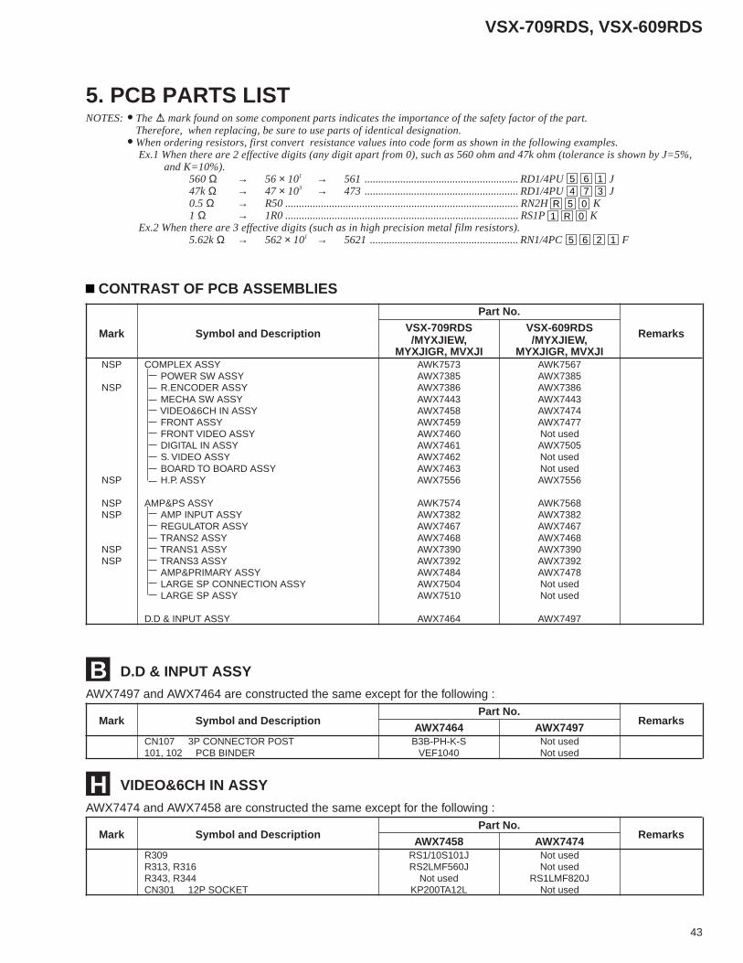
Mark No. Description Part No. Mark No. Description Part No.
5. PCB PARTS LISTNOTES:•The mark found on some component parts indicates the importance of the safety factor of the part.
Therefore, when replacing, be sure to use parts of identical designation.•When ordering resistors, first convert resistance values into code form as shown in the following examples.
Ex.1 When there are 2 effective digits (any digit apart from 0), such as 560 ohm and 47k ohm (tolerance is shown by J=5%, and K=10%).
560 Ω → 56 × 101 → 561 ........................................................ RD1/4PU 5 6 1 J47k Ω → 47 × 103 → 473 ........................................................ RD1/4PU 4 7 3 J0.5 Ω → R50 ..................................................................................... RN2H R 5 0 K1 Ω → 1R0 ..................................................................................... RS1P 1 R 0 K
Ex.2 When there are 3 effective digits (such as in high precision metal film resistors).5.62k Ω → 562 × 101 → 5621 ...................................................... RN1/4PC 5 6 2 1 F
Part No.
Mark Symbol and Description VSX-709RDS VSX-609RDS Remarks/MYXJIEW, /MYXJIEW,MYXJIGR, MVXJI MYXJIGR, MVXJI
NSP COMPLEX ASSY AWK7573 AWK7567 POWER SW ASSY AWX7385 AWX7385
NSP R.ENCODER ASSY AWX7386 AWX7386 MECHA SW ASSY AWX7443 AWX7443 VIDEO&6CH IN ASSY AWX7458 AWX7474 FRONT ASSY AWX7459 AWX7477 FRONT VIDEO ASSY AWX7460 Not used DIGITAL IN ASSY AWX7461 AWX7505 S. VIDEO ASSY AWX7462 Not used BOARD TO BOARD ASSY AWX7463 Not used
NSP H.P. ASSY AWX7556 AWX7556
NSP AMP&PS ASSY AWK7574 AWK7568NSP AMP INPUT ASSY AWX7382 AWX7382
REGULATOR ASSY AWX7467 AWX7467 TRANS2 ASSY AWX7468 AWX7468
NSP TRANS1 ASSY AWX7390 AWX7390NSP TRANS3 ASSY AWX7392 AWX7392
AMP&PRIMARY ASSY AWX7484 AWX7478 LARGE SP CONNECTION ASSY AWX7504 Not used LARGE SP ASSY AWX7510 Not used
D.D & INPUT ASSY AWX7464 AWX7497
CONTRAST OF PCB ASSEMBLIES
D.D & INPUT ASSYBAWX7497 and AWX7464 are constructed the same except for the following :
Mark Symbol and DescriptionPart No.
RemarksAWX7464 AWX7497
CN107 3P CONNECTOR POST B3B-PH-K-S Not used101, 102 PCB BINDER VEF1040 Not used
VIDEO&6CH IN ASSYHAWX7474 and AWX7458 are constructed the same except for the following :
Mark Symbol and DescriptionPart No.
RemarksAWX7458 AWX7474
R309 RS1/10S101J Not usedR313, R316 RS2LMF560J Not usedR343, R344 Not used RS1LMF820JCN301 12P SOCKET KP200TA12L Not used

44
VSX-709RDS, VSX-609RDS
Mark No. Description Part No. Mark No. Description Part No.
Mark No. Description Part No. Mark No. Description Part No.
AMP INPUT ASSYOTHERS
CN290 17P CONNECTOR 52044-1745CN291 16P SOCKET KP200TA16L
D.D & INPUT ASSYSEMICONDUCTORS
IC1101 CS4226-KQ(J)IC1301 KM68257EJ-15IC108 M5216FPIC103 M62446FPIC1001 NJM2100M
IC1602–IC1604,IC1701–IC1705 NJM4558MDIC1401 PQ20WZ51IC102 TC9163AFIC1601 TC9164AFIC101 TC9273F-007
IC104–IC107 UPC4570G2IC1201 YSS912CQ101, Q102 2SC2412KQ1001, Q1002, Q105–Q112 2SC3326Q1601–Q1606 2SC3326
Q1003, Q1101, Q1607, Q1608, Q1610 DTA124EKQ1004, Q1102, Q1609 DTC124EKD1601, D1602 1SS181D103, D105, D106 1SS355D104 UDZS5.1B
D101, D102 UDZS6.8B
COILS AND FILTERSL1401 CHIP SOLID INDUCTOR ATL7002F1101, F1123, F1124, F1203, F1204 DTF1064F1302, F1601, F1602 CHIP BEAD DTF1064F101, F111, F112 CHIP BEAD DTF1067L1101–L1104 QTL1013
CHIP SOLID INDUCTOR
CAPACITORSC101–C114, C1207, C1209, C1213 CCSQCH101J50C1217, C1218, C1221, C1303 CCSQCH101J50C1640, C1641, C197, C198 CCSQCH101J50C207, C208 CCSQCH101J50C211, C212 CCSQCH220J50
C1119 CCSQCH271J50C1123, C1124 CCSQCH331J50C1118, C1130, C1639 CCSQCH471J50C1001, C1002, C121, C1212, C122 CCSRCH101J50C1223, C123, C126–C128 CCSRCH101J50
PCB PARTS LIST FOR VSX-709RDS UNLESS OTHERWISE NOTED
FRONT ASSYKAWX7477 and AWX7459 are constructed the same except for the following :
Mark Symbol and DescriptionPart No.
RemarksAWX7459 AWX7477
R428 Not used RS1/10S472JR429 RS1/10S0R0J RS1/10S751J
AMP&PRIMARY ASSYCAWX7478 and AWX7484 are constructed the same except for the following :
Mark Symbol and DescriptionPart No.
RemarksAWX7484 AWX7478
C757–C759 Not used CQMBA472J50C769 CKCYB102K50 Not usedR757 Not used RD1/4PU223JR758 Not used RD1/4PU222JCN751 SPEAKER TERMINAL 6-P Not used AKE7020
CN753 PIN JACK 1-P Not used AKB7042CN784 10P SOCKET KP250NA10 Not used
DIGITAL IN ASSYJAWX7505 and AWX7461 are constructed the same except for the following :
Mark Symbol and DescriptionPart No.
RemarksAWX7461 AWX7505
C1903 CKSQYB104K25 Not usedR1903 RS1/10S101J Not usedJA1904 OPTICAL LINK OUT GP1F32T Not used
B
A

45
VSX-709RDS, VSX-609RDS
Mark No. Description Part No. Mark No. Description Part No.C152–C154, C159, C160 CCSRCH101J50C163, C164 CCSRCH101J50C1102, C1736 CCSRCH102J50C1707, C1708, C1721, C1722, C173 CCSRCH151J50C1735, C174 CCSRCH151J50
C1113, C1114 CCSRCH180J50C1203, C1204 CCSRCH200J50C1601, C1602, C1609, C1610, C167 CCSRCH221J50C1623 CCSRCH271J50C1103, C1104 CCSRCH390J50
C1101, C1106, C1110, C1210 CCSRCH471J50C1603, C1604, C1611, C1612 CCSRCH471J50C130–C137, C146 CEAT100M50C1116, C1121, C1122, C1201, C1404 CEAT101M10C157, C175, C176 CEAT101M16
C1112 CEAT1R0M50C1713, C1714, C1727, C1728 CEAT220M25C1739, C1740 CEAT220M25C1005, C1202 CEAT221M6R3C144, C145, C147–C151, C205 CEAT3R3M50
C117, C118, C161, C162 CEAT470M25C165, C166, C169 CEAT470M25C155, C156 CEAT471M10C1003, C1004, C115, C116, C1401 CEAT4R7M50C1605, C1606, C1613, C1614 CEAT4R7M50
C1625, C1626, C170, C194, C195 CEAT4R7M50C201 CEAT4R7M50C1115 CEATR47M50C1301 CEJA101M10C1007, C1008 CEJANP100M10
C1129, C1132, C1206, C1208 CKSQYB103K50C1215, C1216, C1220, C1302 CKSQYB103K50C1607, C1608, C1619, C1620 CKSQYB103K50C1629, C1630, C177–C180, C183 CKSQYB103K50C186–C193, C199 CKSQYB103K50
C1108 CKSQYB224K16C140, C143 CKSQYB334K16C1009, C1111, C1117, C1133, C1219 CKSQYF104Z25C1224, C1225, C1228, C1229, C1231 CKSQYF104Z25C1304, C1631, C1632, C209 CKSQYF104Z25
C184, C185 CKSQYF473Z50C1006, C1128, C1134, C119, C120 CKSRYB103K50C1205, C1211, C1214, C1222 CKSRYB103K50C124, C125, C158, C1636, C1637 CKSRYB103K50C1642, C1709, C171, C1710–C1712 CKSRYB103K50
C172, C1723–C1726, C1737, C1738 CKSRYB103K50C1705, C1706, C1719, C1720 CKSRYB104K16C1733, C1734 CKSRYB104K16C1621 CKSRYB122K50C168 CKSRYB152K50
C139, C142 CKSRYB153K50C1615–C1618, C1627, C1703, C1704 CKSRYB222K50C1717, C1718, C1731 CKSRYB222K50C1107 CKSRYB223K50C1701, C1702, C1715, C1716, C1729 CKSRYB682K50
C1732 CKSRYB682K50C138, C141 CKSRYB822K50C1105, C1109, C1226, C1227, C1230 CKSRYF104Z16C1232, C202 CKSRYF104Z16C1628 CKSRYF104Z50
RESISTORSR1302, R1689 RS1/10S0R0JR211, R212 RS1/10S100JR1206–R1208, R1638–R1640 RS1/10S102JR115–R118, R121, R122 RS1/10S104JR132–R135, R139–R143 RS1/10S104J
R157, R158, R163, R164 RS1/10S104JR185, R186, R192, R193 RS1/10S104JR183 RS1/10S122JR144 RS1/10S204JR103, R104, R111, R112 RS1/10S222J
R101, R102, R105–R110 RS1/10S331JR113, R114, R129, R130 RS1/10S331JR1211–R1213 RS1/10S472JR138, R1641, R1713, R1714 RS1/10S473JR1727, R1728, R1741, R1742, R182 RS1/10S473J
R174, R175 RS1LMF101JOther Resistors RS1/16S&&&J
OTHERSCN1501 CONNECTOR 6P 52045-0645CN104, CN105 13P CONNECTOR 52045-1345CN106 17P CONNECTOR 52045-1745CN103 19P CONNECTOR 52045-1945CN102 32P CONNECTOR 52045-3245
JA101–JA104 PIN JACK(4P) AKB7048CN107 3P CONNECTOR POST B3B-PH-K-SCN101 19P SOCKET KP200TA19L101, 102 PCB BINDER VEF1040X1101 CRYSTAL RESONATOR RSS1052
(18.432MHz)
X1201 CRYSTAL RESONATOR VSS1140(12.288MHz)
AMP&PRIMARY ASSYSEMICONDUCTORS IC52 PROTECTOR (315mA) AEK7003 IC603 PROTECTOR (1A) AEK7009
IC51 NJM78M56FA IC601 PAC010A IC602 PAC011A
Q703 2SA1145Q702 2SB1238XQ691, Q692 2SC1740SQ704 2SC1845Q605, Q606, Q633, Q655, Q656 2SC2240
Q601–Q604, Q631, Q632 2SC2878Q651–Q654 2SC2878Q701 2SD1859XQ51 KRC101MD56, D57, D601–D604 1SS133
D631, D632, D651–D654 1SS133D751–D758 1SS133
D701, D702 D5SBA20(B)D711 MTZJ22DD58 MTZJ5.1A
D712 MTZJ5.1BD605, D606, D633, D634 MTZJ8.2A
D51–D55 S5688G
C
46
VSX-709RDS, VSX-609RDS
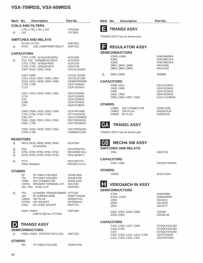
Mark No. Description Part No. Mark No. Description Part No.
COILS AND FILTERSL751–L753, L761, L762 ATH1004
L52 XTF3001
SWITCHES AND RELAYSRY751–RY754 ASR7001
RY51 JOE LOWPOWER RELAY ASR7013
CAPACITORSC707, C708 (0.01µF/AC250V) ACG1005
C51, C52 (10000pF/AC250V) ACG7020C701, C702 (4700µF/63V) ACH7134C703, C704 (3300µF/42V) ACH7135C607–C610, C634, C635 CCCSL120J50
C657–C660 CCCSL120J50C613, C614, C637, C663, C664 CCCSL221J50C615, C616, C638, C665, C666 CEANP2R2M50C705, C706 CEAT100M2AC712 CEAT101M10
C611, C612, C636, C661, C662 CEAT101M16C711 CEAT101M35C53 CEAT102M16C692 CEAT221M10C54 CEAT470M25
C605, C606, C633, C655, C656 CEAT4R7M50C751–C756, C761–C764 CFTYA224J50C55–C57 CGCYX103M25C601, C602, C631, C651, C652 CKCYB102K50C691, C769 CKCYB102K50
C603, C604, C632, C653, C654 CKCYB331K50C765–C768 CQMBA472J50
RESISTORS R615, R616, R638, R665, R666 ACN7094
(0.22Ω/5W) R52 RD1/2PM270J R751, R752, R755, R761, R762 RD1/4PMF101J R753, R754, R756, R763, R764 RS1LMF4R7J
R711 RS2LMF272JOther Resistors RD1/4PU&&&J
OTHERS53 3P CABLE HOLDER 51048-0300701 7P CABLE HOLDER 51048-0700CN53 22P CONNECTOR 52045-2245CN754 SPEAKER TERMINAL 8-P AKE7057H51, H52 FUSE CLIP AKR7001
T51 STANDBY TRANSFORMER ATT7037J44 3P JUMPER WIRE D20PYY0325ECN601 16P PLUG KM200TA16CN784 10P SOCKET KP250NA10CN51 AC CODE SOCKET RKP1751
KN51, KN601 VNF1084EARTH METAL FITTING
TRANS2 ASSYSEMICONDUCTORS IC851–IC853 PROTECTOR (1.6A) AEK7012
OTHERS851 7P CABLE HOLDER 51048-0700
TRANS3 ASSY
TRANS3 ASSY has no service part.
REGULATOR ASSYSEMICONDUCTORS
IC803, IC804 NJM78M05FAIC801 NJM78M12FAIC802 NJM79M12FAQ801, Q803, Q805 KRA103MQ802, Q804, Q806 KRC101M
D801–D808 S5688G
CAPACITORSC808, C811 CEAT101M10C805, C806 CEAT101M16C809 CEAT222M16C801, C802 CEAT222M25C803, C804, C807, C810 CGCYX103M25
OTHERSCN801 22P CONNECTOR 52045-2245CN802 19P PLUG KM200TA19CN803 5P PLUG KM200TA5
TRANS1 ASSY
TRANS1 ASSY has no service part.
MECHA SW ASSYSWITCHES AND RELAYS
S591 ASG7014
CAPACITORSC591, C592 CKSQYF103Z50
OTHERSCN591 52151-0310
VIDEO&6CH IN ASSYSEMICONDUCTORS
IC301 NJM2296MIC302, IC303 NJM4558MDQ302 2SA1515Q303 2SC2878Q301 2SC3377
D301, D302, D305, D306 1SS355D303, D304 UDZS6.2B
CAPACITORSC319, C320, C327, C328 CCSQCH101J50C342–C345 CCSQCH101J50C347 CCSQCH470J50C307–C310, C312, C314, C338 CEAT470M25C321, C324, C331, C332 CEAT4R7M50
D
E
F
H
GA
GB

47
VSX-709RDS, VSX-609RDS
Mark No. Description Part No. Mark No. Description Part No.C302, C315, C316, C322, C323 CKSQYB103K50C329, C330 CKSQYB103K50C346 CKSQYB104K16C304–C306, C317, C318 CKSQYB221K50C325, C326 CKSQYB221K50
C333 CKSQYB331K50C311, C313 CKSQYB473K50
RESISTORS R313, R316 RS2LMF560J
Other Resistors RS1/10S&&&J
OTHERSCN303 13P CONNECTOR 52044-1345CN307 PIN JACK(4P) AKB7087CN305 6P PIN JACK AKB7123CN301 12P SOCKET KP200TA12LCN302 5P SOCKET KP200TA5L
JA301 JACK RKN1004
H.P. ASSYSEMICONDUCTORS
Q551, Q552 2SC2878
CAPACITORSC553 CCSQCH471J50C552 CKSQYB103K50C551 CKSQYB104K16C555, C556 CKSQYB223K50
RESISTORS R551, R552 RS1/2LMF121J
Other Resistors RS1/10S&&&J
OTHERS551 CABLE HOLDER(4P) 51063-0405JA551 JACK RKN1002
DIGITAL IN ASSYSEMICONDUCTORS
IC1901 TC74ACT151FIC1902 TC74HCU04AF
COILS AND FILTERSF1901–F1904 CHIP BEAD DTF1067
CAPACITORSC1917 CCSQCH220J50C1918 CCSQCH221J50C1907, C1914 CCSQCH271J50C1916 CCSQCH471J50C1911 CCSQCH560J50
C1904, C1905, C1912 CEAT101M10C1915 CKSQYB102K50C1906, C1910, C1913, C1919, C1920 CKSQYB103K50C1922 CKSQYB103K50C1901–C1903, C1908, C1909, C1921 CKSQYB104K25
RESISTORSAll Resistors RS1/10S&&&J
OTHERSCN1901 CONNECTOR 6P 52045-0645JA1902,JA1903 GP1F32R
OPTICAL RECEIV MOD.JA1904 OPTICAL LINK OUT GP1F32TJA1901 JACK VKB1077
FRONT ASSYSEMICONDUCTORS
IC481 BU1923FIC401 PDG247BQ481 2SA1515Q405 2SA933SQ483 2SC1740S
Q401, Q402, Q442, Q471 KRA103MQ403, Q441, Q482 KRC101MD407, D408, D442 1SS355D403, D405 DAN217D401, D404 DAP202K
COILS AND FILTERSL401, L481 LFEA2R2J
SWITCHES AND RELAYSS451–S477 XSG3001
CAPACITORSC404 (0.047F/5.5V) ACH7017C420 (220µF/35V) ACH7101C489, C490 CCSQCH270J50C483, C487 CEAT101M10C486 CEAT1R0M50
C402, C405 CEAT221M6R3C409, C410, C484 CEAT2R2M50C412 CEAT470M50C442 CEJA470M10C451–C454, C481, C482, C495 CKSQYB102K50
C401, C403, C411, C441, C531 CKSQYB103K50C408, C416, C418, C491–C494 CKSQYB104K16C532 CKSQYB223K25C485 CKSQYB472K50C406, C407 CKSQYB473K16
C488 CKSQYB561K50
RESISTORSAll Resistors RS1/10S&&&J
OTHERS491 CABLE HOLDER(3P) 51063-0305403, 471 CABLE HOLDER(4P) 51063-0405CN401 19P CONNECTOR 52044-1945CN402 32P CONNECTOR 52044-3245V401 FL TUBE AAV7072
X481 CRYSTAL RESONATOR ASS7004(4.332MHz)
X401 CERAMIC RESONATOR ASS7018(7.2MHz)
401 REMOTE RECEIVER UNIT GP1U27X
I
J
K
48
VSX-709RDS, VSX-609RDS
Mark No. Description Part No. Mark No. Description Part No.
6. ADJUSTMENTThere is no information to be shown in this chapter.
R.ENCODER ASSYSWITCHES AND RELAYS
S511 ASX7004
OTHERS511 CABLE HOLDER(3P) 51063-0305
POWER SW ASSYSEMICONDUCTORS
D501 BR3371XJ30A
SWITCHES AND RELAYSS501 XSG3001
RESISTORSAll Resistors RS1/10S&&&J
OTHERS501 CABLE HOLDER(4P) 51063-0405
S. VIDEO ASSYSEMICONDUCTORS
IC351, IC352 NJM2296MD351–D354 1SS355
CAPACITORSC375, C376 CCSQCH470J50C352, C355, C358, C361–C363 CEAT470M25C366 CEAT470M25C372, C373 CKSQYB103K50C353, C356, C359, C360 CKSQYB104K25
C364, C365, C368–C371 CKSQYB221K50
RESISTORSAll Resistors RS1/10S&&&J
OTHERSCN353 MINI DIN SOCKET 2P AKP7020CN352 MINI DIN SOCKET 3P AKP7043CN354 CONNECTOR POST B5B-PH-K-SCN351 12P SOCKET KP200TA12L
BOARD TO BOARD ASSYOTHERS
CN390, CN391 12P PLUG KM200TA12
FRONT VIDEO ASSYCAPACITORS
C903, C905 CEAT470M25C908, C911, C914 CKSQYB103K50C904, C906, C909, C912 CKSQYB104K25C901, C902 CKSQYB221K50C907, C910, C913 CKSQYB471K50
M
L
N
O
P
RESISTORSAll Resistors RS1/10S&&&J
OTHERSCN902 PIN JACK(4P) AKX7007KN901 EARTH METAL FITTING VNF1084
LARGE SP CONNECTION ASSYOTHERS
CN785, CN786 10P PLUG KM250NA10L
LARGE SP ASSYCAPACITORS
C781–C783 CQMBA472J50
RESISTORSAll Resistors RD1/4PU&&&J
OTHERSCN782 PIN JACK 1P AKB7042CN781 SPEAKER TERMINAL 6P AKE7056CN783 10P SOCKET KP250NA10
Q
R
49
VSX-709RDS, VSX-609RDS
2 ×2
Remove the Bonnet (seven screws).1
Rear PanelPull up
2
2
4
Diagnosis
AMP&PRIMARY Assy
REGULATOR Assy
Heat Sink
5
×22 ×3
2 ×5
3 ×3
×2
2 ×3
7.1 DISASSEMBLY7. GENERAL INFORMATION
Diagnosis
PCB Location
AMP&PRIMARY Assy
FRONT Assy
FRONT VIDEO Assy
AMP INPUT Assy
D.D & INPUT Assy
VIDEO&6CH IN Assy
FM/AM TUNER Unit
REGULATOR Assy
DIGITAL IN Assy
H.P. Assy
TRANS 3 Assy
TRANS 2 Assy
TRANS 1 Assy
PR. ENCODER Assy L
A
BH
LARGE SP Assy R
S.VIDEO Assy N
F
K
J
IEGAD
C
POWER SW AssyMMECHA SW AssyGB
Note : This photograph shows other models. However, the work method is the same.
50
VSX-709RDS, VSX-609RDS
PDG247A (FRONT ASSY : IC401) • System Control MCU
• Pin Arrangement (Top View)
• The information shown in the list is basic information and may not correspond exactly to that shown in the schematic diagrams.
7.2 PARTS7.2.1 IC
1G2
G1
NC
ACIN
RDS_DT
RDS_CK
OVFB
RMC
MRIN
PLL_CE
CDC_CS
CDC_CK
CDC_DO
CDC_DI
STEREO
TUNED
ENC_A
ENC_B
A.MUTE
CSB
DSP_CS
DSP_CK
DSP_SI
DSP_SO
VER_2
ST_EVR
PLL_DO
KEYIN1
KEYIN2
G1/A1
G0/A0
NC
PE0/EC0/INT0
PE1/EC1/INT1
PE2/INT2
PE3/INT3/NMI
PE4/RMC
PE5
PE6/PWM
PE7/TO/ADJ
PC0/KR0
PC1/KR1
PC2/KR2
PC3/KR3
PC4/KR4
PC5/KR5
PC6/KR6
PC7/KR7
PB0/CINT
PB1/CS0
PB2/SCK0
PB3/SI0
PB4/SO0
PB5/SCK1
PB6/SI1
PB7/SO1
AVREF
PA1/AN0
PA1/AN1
KE
YIN
3
KE
YIN
4
VE
RS
ION
AM
P_D
C
AM
P_O
L
MV
RA
TT
VID
EO
1
VID
EO
2
VID
EO
3
SY
S_C
K
SY
S_D
T
PA
2/A
N2
PA
3/A
N3
PA
4/A
N4
PA
5/A
N5
PA
6/A
N6
PA
7/A
N7
AV
SS
RS
T
EX
TA
L
XT
AL
VS
S
TX
TE
X
VD
D
VF
IP
PD
0/A
55
PD
1/A
54
PD
2/A
53
PD
3/A
52
PD
4/A
51
A21
A22
A23
PH7/A24
PH6/A25
PH5/A26
PH4/A27
PH3/A28
PH2/A29
PH1/A30
PH0/A31
PG7/A32
PG6/A33
PG5/A34
PG4/A35
PG3/A36
PG2/A37
PG1/A38
PG0/A39
PF7/A40
PF6/A41
PF5/A42
PF4/A43
PF3/A44
PF2/A45
PF1/A46
PF0/A47
PD7/A48
PD6/A49
PD5/A50
S11
S12
S13
S14
S15
S16
S17
S18
S19
S20
S21
S22
RY_B
RY_C/R
RY_A
RY_AC
GAIN
NECK
DSP_RST
9164_CS
T_MUTE
T_POWON
FM+(RDS)
CDC_RST
DSP_MT
9273_CS
D_MUTE
G2/
A2
G3/
A3
G4/
A4
G5/
A5
G6/
A6
G7/
A7
G8/
A8
G9/
A9
G10
/A10
G11
/A11
G12
/A12
VD
D
G13
/A13
G14
/A14
G15
/A15
A16
A17
A18
A19
A20
G3
G4
G5
G6
G7
G8
G9
G10
S1
S2
S3
S4
S5
S6
S7
S8
S9
S10
2
3
4
5
6
7
8
9
10
11
12
13
14
15
16
17
18
19
20
100
99 98 97 96 95 94 93 92 91 90 89 88 87 86 85 84 83 82 81
31 32 33 34 35 36 37 38 39 40 41 42 43 44 45 46 47 48 49 50
21
22
23
24
25
26
27
28
29
30
80
79
78
77
76
75
74
73
72
71
70
69
68
67
66
65
64
63
62
61
60
59
58
57
56
55
54
53
52
51
51
VSX-709RDS, VSX-609RDS
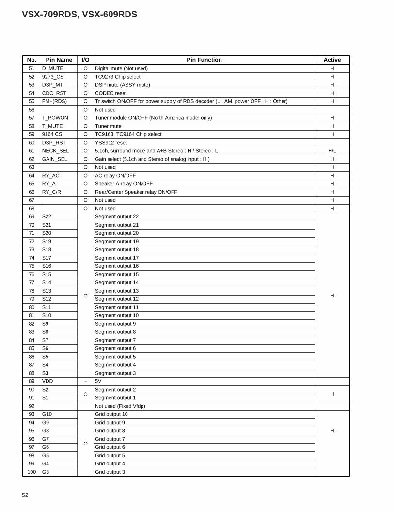
No. Pin Name I/O Pin Function Active1 G2 O Grid output 2 H
2 G1 O Grid output 1 H
3 NC − Connect to VDD
4 ACIN I AC pulse input
5 RDS_DT I Serial control DATA signal of RDS communication
6 RDS_CK I Serial control CLOCK signal of RDS communication
7 DIRLOCK I ERR/OVER input from CODEC
8 RMC I Remote control signal input (no-carrier signal)
9 MRIN I MULTI-ROOM input
10 PLL_CE O Chip select signal for communication with LC72131 (tuner) H
11 CDC_CS O CODEC chip serect
12 CDC_CK O CODEC, TC9164 control clock
13 CDC_DO O CODEC, TC9164 control data output
14 CDC_DI I Data input from CODEC
15 STEREO I Stereo/Monoral signal judgment signal
16 TUNED I TUNED information
17 ENC_A I Rotary encoder signal input A
18 ENC_B I Rotary encoder signal input B
19 AMUTE O Audio mute L
20 CSB O Chip select for control of YSS912 sub DSP L
21 DSP_CS O Chip select for control of YSS912 main DSP L
22 DSP_CK O Clock signal for communication with YSS912 H
23 DSP_SI I DATA input for communication with YSS912
24 DSP_SO O DATA output signal for communication with YSS912 H
25 VER_2 I Destination switch 2
26 ST_EVR O Strobe signal for communication with electric volume IC H
27 PLL_DO I Data input signal for communication with LC72131 (tuner)
28 AVref − Connect to VDD
29 KEYIN1 I Key input A/D conversion port 1
30 KEYIN2 I Key input A/D conversion port 2
31 KEYIN3 I Key input A/D conversion port 3
32 KEYIN4 I Key input A/D conversion port 4
33 VER 1 I Destination switch (A/D input)
34 AMP_DC I DC abnormality detection of protection circuit (L : Abnormality detection) L
35 AMP_OL I Over-load detection of protection circuit (L : Abnormality detection) L
36 MVRATT O ATT control of master volume (L : Less than -15dB) H
37 AVSS − Connect to VSS
38 RST − Reset
39 EXTAL −Connect to the oscillator (7.2MHz)
40 XTAL −41 VSS − Connect to VSS
42 TX − Open
43 TEX − Connect to VSS
44 VDD − +5V
45 VFDP − -30V
46 VIDEO1
O NJM2296D control H47 VIDEO2
48 VIDEO3
49 SYS_DT O Data signal for communication with M62446, TC9163, TC9164 and PLL H
O Clock signal for communication with M62446, TC9163, TC9164 and PLL H50 SYS_CK
• Pin Function
52
VSX-709RDS, VSX-609RDS
No. Pin Name I/O Pin Function Active51 D_MUTE
O TC9273 Chip select
O Digital mute (Not used)
O DSP mute (ASSY mute)
H
H
H
52 9273_CS
53 DSP_MT
54 CDC_RST O CODEC reset H
55 FM+(RDS) O Tr switch ON/OFF for power supply of RDS decoder (L : AM, power OFF , H : Other) H
56 O Not used
57 T_POWON O Tuner module ON/OFF (North America model only) H
58 T_MUTE O Tuner mute H
59 9164 CS O TC9163, TC9164 Chip select H
60 DSP_RST O YSS912 reset
61 NECK_SEL O 5.1ch, surround mode and A+B Stereo : H / Stereo : L H/L
62 GAIN_SEL O Gain select (5.1ch and Stereo of analog input : H ) H
63 O Not used H
64 RY_AC O AC relay ON/OFF H
65 RY_A O Speaker A relay ON/OFF H
66 RY_C/R O Rear/Center Speaker relay ON/OFF H
67 O Not used H
68 O Not used H
69 S22
O
Segment output 22
H
70 S21 Segment output 21
71 S20 Segment output 20
72 S19 Segment output 19
73 S18 Segment output 18
74 S17 Segment output 17
75 S16 Segment output 16
76 S15 Segment output 15
77 S14 Segment output 14
78 S13 Segment output 13
79 S12 Segment output 12
80 S11 Segment output 11
81 S10 Segment output 10
82 S9 Segment output 9
H
83 S8 Segment output 8
84 S7 Segment output 7
85 S6 Segment output 6
86 S5 Segment output 5
87 S4 Segment output 4
88 S3 Segment output 3
89 VDD − 5V
90 S2
O
OSegment output 2
H
91 S1 Segment output 1
92 Not used (Fixed Vfdp)
93 G10 Grid output 10
94 G9 Grid output 9
95 G8 Grid output 8
96 G7 Grid output 7
97 G6 Grid output 6
98 G5 Grid output 5
99 G4 Grid output 4
100 G3 Grid output 3
53
VSX-709RDS, VSX-609RDS
OUT4
OUT3
OUT2
OUT1
AVDD
SWin
GNDS
SRin
1
2
3
4
5
6
7
8
SLin
GNDC
Cin
GNDR
Rin
GNDL
Lin
BYPASSR
9
10
11
12
13
14
15
16
BYPASSR
LTRE
LBASS3
LBASS2
LBASS1
17
18
19
20
21
MCUI/F
DVDD
CLK
DATA
LATCH
DGND
AGND
SWout
<SW>
Volume17-24kΩ
SRout
42
41
40
39
38
37
36
35
SLout
Cout
Rout
Lout
AVSS
CL1
CL2
CR1
34
33
32
31
30
29
28
27
CR2
RTRE
RBASS3
RBASS2
RBASS1
26
25
24
23
22
<SR>
Volume17-24kΩ
<SL>
Volume17-24kΩ
<C>
Volume17-24kΩ
<R>
<R>
Volume17-24kΩ
70kΩ
70kΩ
<L>
Volume17-24kΩ
S
T70
kΩ70
kΩ
70kΩ
12kΩ
12kΩ
300kΩ
1.5k
Ω
S
T
<L>70kΩ
12kΩ
12kΩ
300kΩ
1.5k
Ω
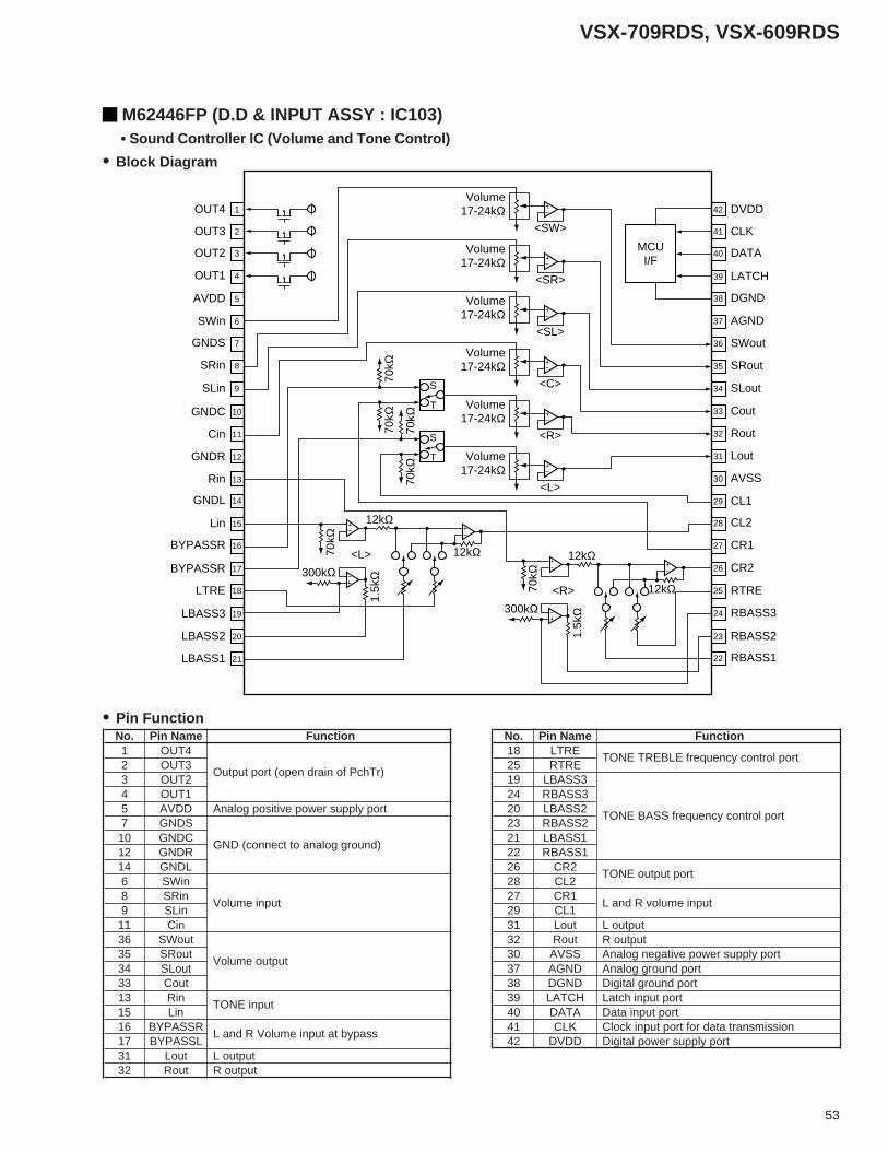
M62446FP (D.D & INPUT ASSY : IC103) • Sound Controller IC (Volume and Tone Control)
• Pin Function
• Block Diagram
No. Pin Name Function1 OUT42 OUT3
Output port (open drain of PchTr)3 OUT24 OUT15 AVDD Analog positive power supply port7 GNDS
10 GNDCGND (connect to analog ground)
12 GNDR14 GNDL6 SWin8 SRin
Volume input9 SLin
11 Cin36 SWout35 SRout
Volume output34 SLout33 Cout13 Rin
TONE input15 Lin16 BYPASSR
L and R Volume input at bypass17 BYPASSL31 Lout L output32 Rout R output
No. Pin Name Function18 LTRE
TONE TREBLE frequency control port25 RTRE19 LBASS324 RBASS320 LBASS2
TONE BASS frequency control port23 RBASS221 LBASS122 RBASS126 CR2
TONE output port28 CL227 CR1
L and R volume input29 CL131 Lout L output32 Rout R output30 AVSS Analog negative power supply port37 AGND Analog ground port38 DGND Digital ground port39 LATCH Latch input port40 DATA Data input port41 CLK Clock input port for data transmission42 DVDD Digital power supply port
54
VSX-709RDS, VSX-609RDS
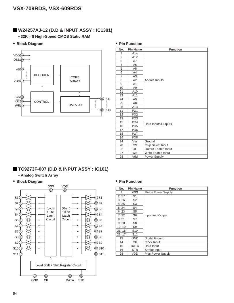
W24257AJ-12 (D.D & INPUT ASSY : IC1301) • 32K × 8 High-Speed CMOS Static RAM
• Block Diagram • Pin Function
VDDDSS
A0
A14
28
14
10
1
20
22
27
I/O819
I/O111CSOEWE
DECORER
DATA I/O
COREARRAY
CONTROL
No. Pin Name Function1 A142 A123 A74 A65 A56 A47 A38 A2 Addres Inputs9 A110 A021 A1023 A1124 A925 A826 A1311 I/O112 I/O213 I/O315 I/O4
Data Inputs/Outputs16 I/O517 I/O618 I/O719 I/O814 Vss Ground20 CS Chip Select Input22 OE Output Enable Input27 WE Write Enable Input28 Vdd Power Supply
TC9273F-007 (D.D & INPUT ASSY : IC101) • Analog Switch Array
• Block Diagram • Pin FunctionVDDDSS
S1
281
CKGND
1413
STBDATA
1615
2
S2 3
S3 4
S4 5
S5 6
S6 7
S7 8
S8 9
S9 10
Level Shift + Shift Register Circuit
(L-ch)10 bitLatchCircuit
(R-ch)10 bitLatchCircuit
S10 11
S11
S1
S2
S3
S4
S5
S6
S7
S8
S9
S10
S1112
27
26
25
24
23
22
21
20
19
18
17
No. Pin Name Function1 VSS Minus Power Supply
2, 27 S13, 26 S24, 25 S35, 24 S46, 23 S57, 22 S6 Input and Output8, 21 S79, 20 S8
10, 19 S921, 18 S1026, 17 S11
13 GND Digital Ground14 CK Clock Input15 DATA Data Input16 STB Strobe Input28 VDD Plus Power Supply
55
VSX-709RDS, VSX-609RDS
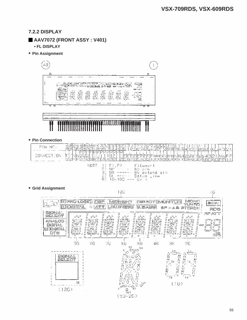
AAV7072 (FRONT ASSY : V401) • FL DISPLAY
7.2.2 DISPLAY
• Pin Assignment
• Pin Connection
• Grid Assignment
56
VSX-709RDS, VSX-609RDS
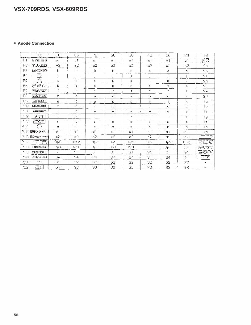
• Anode Connection
57
VSX-709RDS, VSX-609RDS
8.1 PANEL FACILITIES8. PANEL FACILITIES AND SPECIFICATIONS
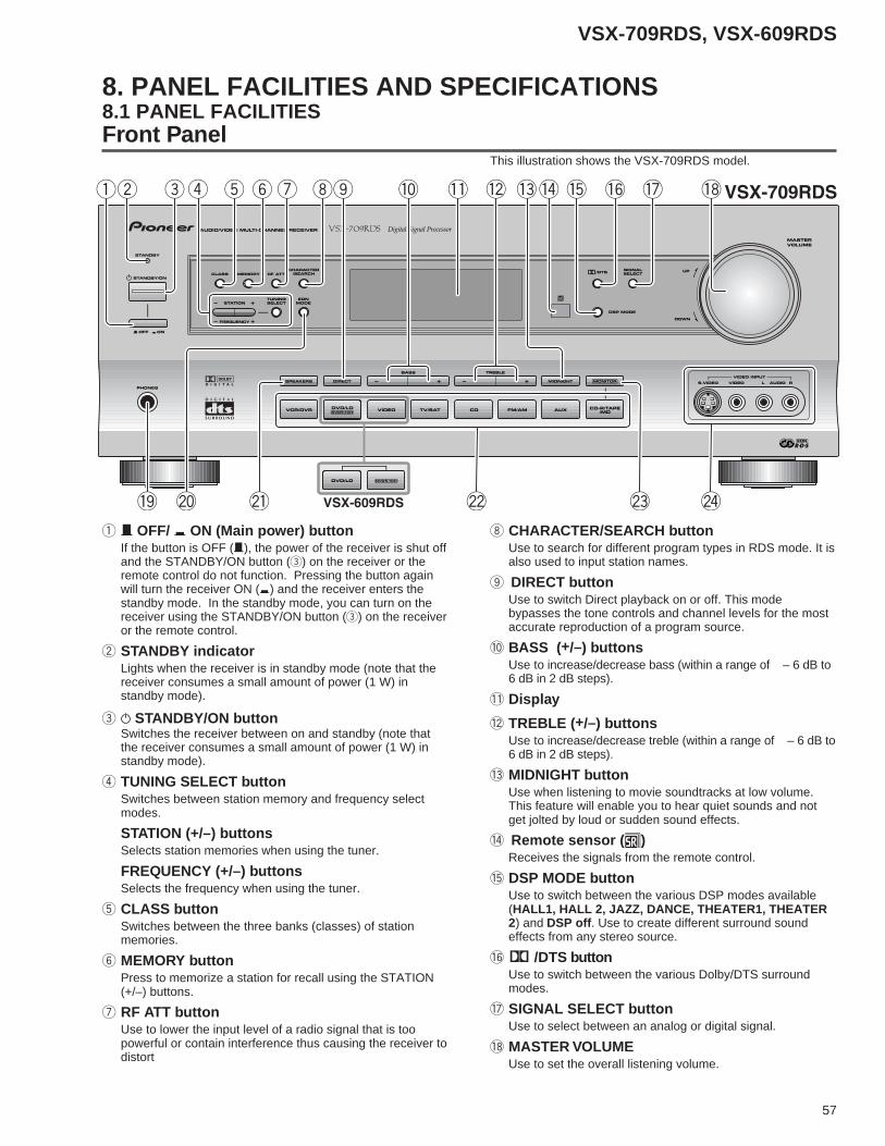
Front PanelThis illustration shows the VSX-709RDS model.
1 — OFF/ _ ON (Main power) buttonIf the button is OFF (—), the power of the receiver is shut offand the STANDBY/ON button (3) on the receiver or theremote control do not function. Pressing the button againwill turn the receiver ON (_) and the receiver enters thestandby mode. In the standby mode, you can turn on thereceiver using the STANDBY/ON button (3) on the receiveror the remote control.
2 STANDBY indicatorLights when the receiver is in standby mode (note that thereceiver consumes a small amount of power (1 W) instandby mode).
3 STANDBY/ON buttonSwitches the receiver between on and standby (note thatthe receiver consumes a small amount of power (1 W) instandby mode).
4 TUNING SELECT buttonSwitches between station memory and frequency selectmodes.
STATION (+/–) buttonsSelects station memories when using the tuner.
FREQUENCY (+/–) buttonsSelects the frequency when using the tuner.
5 CLASS buttonSwitches between the three banks (classes) of stationmemories.
6 MEMORY buttonPress to memorize a station for recall using the STATION(+/–) buttons.
7 RF ATT buttonUse to lower the input level of a radio signal that is toopowerful or contain interference thus causing the receiver todistort
8 CHARACTER/SEARCH buttonUse to search for different program types in RDS mode. It isalso used to input station names.
9 DIRECT buttonUse to switch Direct playback on or off. This modebypasses the tone controls and channel levels for the mostaccurate reproduction of a program source.
0 BASS (+/–) buttonsUse to increase/decrease bass (within a range of – 6 dB to6 dB in 2 dB steps).
- Display
= TREBLE (+/–) buttonsUse to increase/decrease treble (within a range of – 6 dB to6 dB in 2 dB steps).
~ MIDNIGHT buttonUse when listening to movie soundtracks at low volume.This feature will enable you to hear quiet sounds and notget jolted by loud or sudden sound effects.
! Remote sensor ( Î)Receives the signals from the remote control.
@ DSP MODE buttonUse to switch between the various DSP modes available(HALL1, HALL 2, JAZZ, DANCE, THEATER1, THEATER2) and DSP off . Use to create different surround soundeffects from any stereo source.
# 2 /DTS buttonUse to switch between the various Dolby/DTS surroundmodes.
$ SIGNAL SELECT buttonUse to select between an analog or digital signal.
% MASTER VOLUMEUse to set the overall listening volume.
58
VSX-709RDS, VSX-609RDS
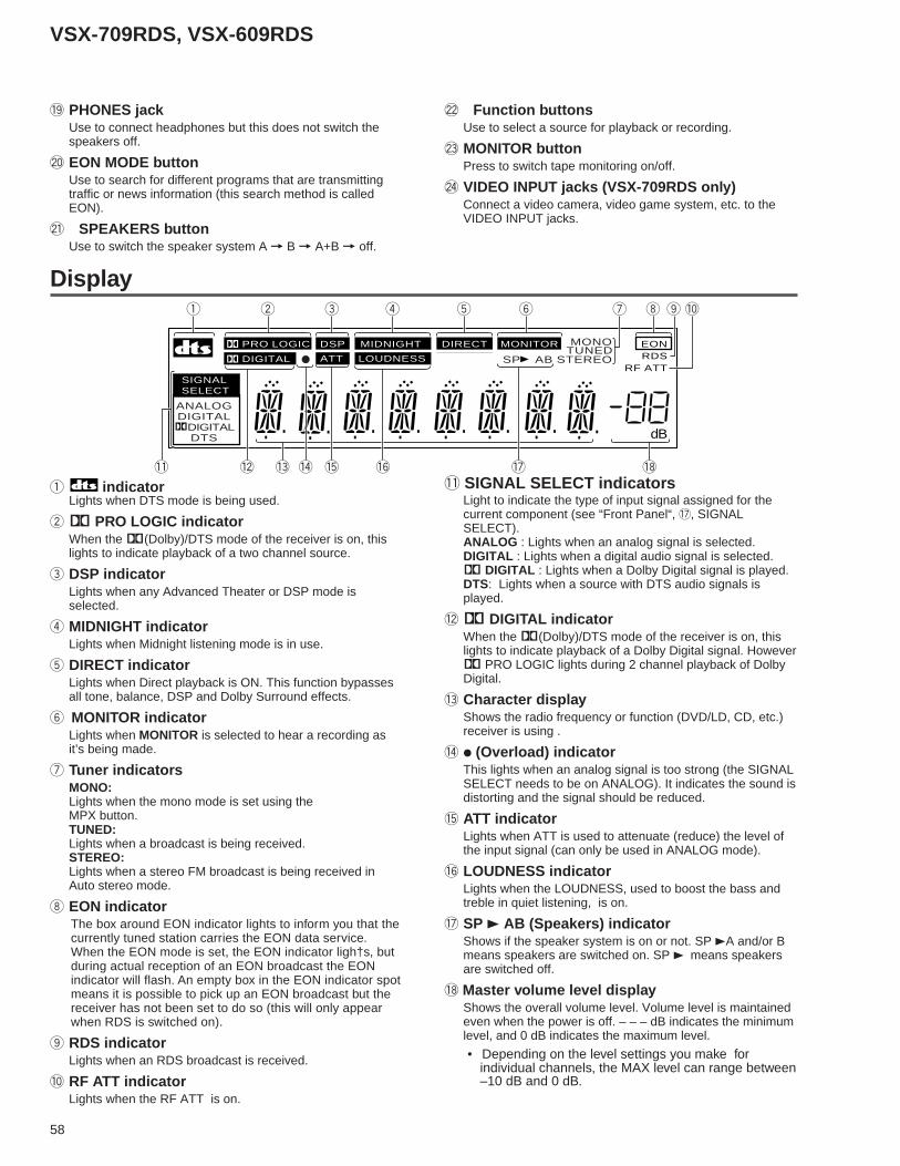
dB
PRO LOGIC
DIGITAL
DSP
ATT
SIGNALSELECT
MIDNIGHT
LOUDNESS
DIRECT
S.BASS
MONITOR EONRDS
RF ATT
TUNEDMONO
ANALOGDIGITAL
DIGITALDTS
SP AB STEREO
Display
^ PHONES jackUse to connect headphones but this does not switch thespeakers off.
& EON MODE buttonUse to search for different programs that are transmittingtraffic or news information (this search method is calledEON).
* SPEAKERS buttonUse to switch the speaker system A = B = A+B = off.
( Function buttonsUse to select a source for playback or recording.
) MONITOR buttonPress to switch tape monitoring on/off.
_ VIDEO INPUT jacks (VSX-709RDS only)Connect a video camera, video game system, etc. to theVIDEO INPUT jacks.
1 indicatorLights when DTS mode is being used.
2 2 PRO LOGIC indicatorWhen the 2(Dolby)/DTS mode of the receiver is on, thislights to indicate playback of a two channel source.
3 DSP indicatorLights when any Advanced Theater or DSP mode isselected.
4 MIDNIGHT indicatorLights when Midnight listening mode is in use.
5 DIRECT indicatorLights when Direct playback is ON. This function bypassesall tone, balance, DSP and Dolby Surround effects.
6 MONITOR indicatorLights when MONITOR is selected to hear a recording asit’s being made.
7 Tuner indicatorsMONO:Lights when the mono mode is set using theMPX button.TUNED:Lights when a broadcast is being received.STEREO:Lights when a stereo FM broadcast is being received inAuto stereo mode.
8 EON indicatorThe box around EON indicator lights to inform you that thecurrently tuned station carries the EON data service.When the EON mode is set, the EON indicator ligh†s, butduring actual reception of an EON broadcast the EONindicator will flash. An empty box in the EON indicator spotmeans it is possible to pick up an EON broadcast but thereceiver has not been set to do so (this will only appearwhen RDS is switched on).
9 RDS indicatorLights when an RDS broadcast is received.
0 RF ATT indicatorLights when the RF ATT is on.
- SIGNAL SELECT indicatorsLight to indicate the type of input signal assigned for thecurrent component (see “Front Panel“, $, SIGNALSELECT).ANALOG : Lights when an analog signal is selected.DIGITAL : Lights when a digital audio signal is selected.2 DIGITAL : Lights when a Dolby Digital signal is played.DTS: Lights when a source with DTS audio signals isplayed.
= 2 DIGITAL indicatorWhen the 2(Dolby)/DTS mode of the receiver is on, thislights to indicate playback of a Dolby Digital signal. However2 PRO LOGIC lights during 2 channel playback of DolbyDigital.
~ Character displayShows the radio frequency or function (DVD/LD, CD, etc.)receiver is using .
! ÷ (Overload) indicatorThis lights when an analog signal is too strong (the SIGNALSELECT needs to be on ANALOG). It indicates the sound isdistorting and the signal should be reduced.
@ ATT indicatorLights when ATT is used to attenuate (reduce) the level ofthe input signal (can only be used in ANALOG mode).
# LOUDNESS indicatorLights when the LOUDNESS, used to boost the bass andtreble in quiet listening, is on.
$ SP 3 AB (Speakers) indicatorShows if the speaker system is on or not. SP 3A and/or Bmeans speakers are switched on. SP 3 means speakersare switched off.
% Master volume level displayShows the overall volume level. Volume level is maintainedeven when the power is off. – – – dB indicates the minimumlevel, and 0 dB indicates the maximum level.
• Depending on the level settings you make forindividual channels, the MAX level can range between–10 dB and 0 dB.
59
VSX-709RDS, VSX-609RDS
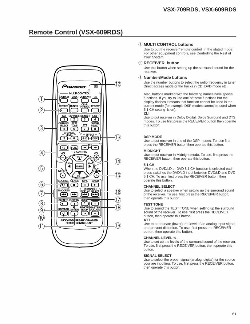
Remote Control (VSX-709RDS)
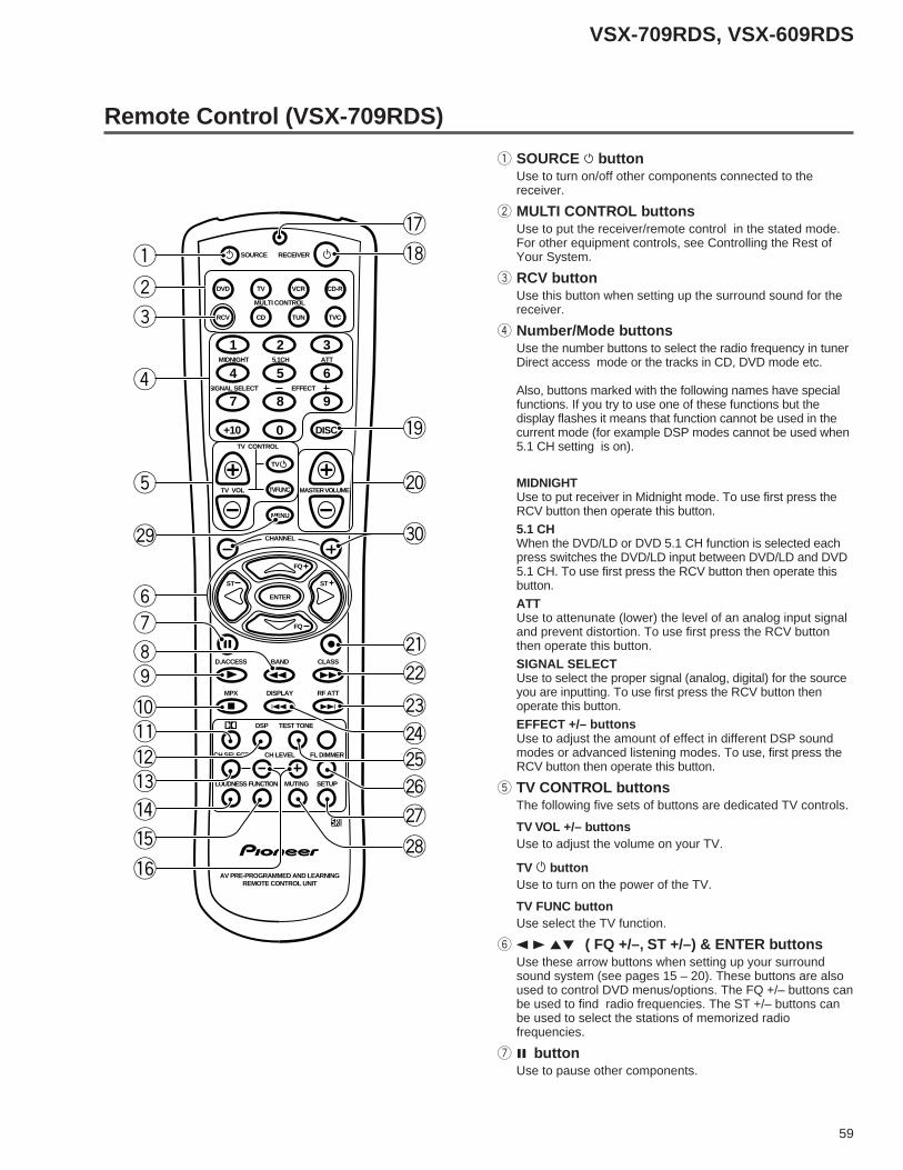
1 SOURCE buttonUse to turn on/off other components connected to thereceiver.
2 MULTI CONTROL buttonsUse to put the receiver/remote control in the stated mode.For other equipment controls, see Controlling the Rest ofYour System.
3 RCV buttonUse this button when setting up the surround sound for thereceiver.
4 Number/Mode buttonsUse the number buttons to select the radio frequency in tunerDirect access mode or the tracks in CD, DVD mode etc.
Also, buttons marked with the following names have specialfunctions. If you try to use one of these functions but thedisplay flashes it means that function cannot be used in thecurrent mode (for example DSP modes cannot be used when5.1 CH setting is on).
MIDNIGHTUse to put receiver in Midnight mode. To use first press theRCV button then operate this button.
5.1 CHWhen the DVD/LD or DVD 5.1 CH function is selected eachpress switches the DVD/LD input between DVD/LD and DVD5.1 CH. To use first press the RCV button then operate thisbutton.
ATTUse to attenunate (lower) the level of an analog input signaland prevent distortion. To use first press the RCV buttonthen operate this button.
SIGNAL SELECTUse to select the proper signal (analog, digital) for the sourceyou are inputting. To use first press the RCV button thenoperate this button.
EFFECT +/– buttonsUse to adjust the amount of effect in different DSP soundmodes or advanced listening modes. To use, first press theRCV button then operate this button.
5 TV CONTROL buttonsThe following five sets of buttons are dedicated TV controls.
TV VOL +/– buttonsUse to adjust the volume on your TV.
TV buttonUse to turn on the power of the TV.
TV FUNC buttonUse select the TV function.
6 2 3 5∞ ( FQ +/–, ST +/–) & ENTER buttonsUse these arrow buttons when setting up your surroundsound system (see pages 15 – 20). These buttons are alsoused to control DVD menus/options. The FQ +/– buttons canbe used to find radio frequencies. The ST +/– buttons canbe used to select the stations of memorized radiofrequencies.
7 8 buttonUse to pause other components.
Î
SOURCE
DISC
MIDNIGHT
SIGNAL SELECT
TV CONTROL
TV VOL TVFUNC
TV
MENU
ENTER
D.ACCESS BAND CLASS
CH SELECT CH LEVEL
AV PRE-PROGRAMMED AND LEARNINGREMOTE CONTROL UNIT
DSP TEST TONE
FL DIMMER
LOUDNESS FUNCTION SETUPMUTING
MPX DISPLAY RF ATT
FQ
FQ
ST ST
CHANNEL
EFFECT
MASTER VOLUME
+10
5.1CH
MULTI CONTROL
ATT
DVD TV VCR CD-R
RCV CD TUN TVC
RECEIVER
1 2 3
4 5 6
7 8 9
7 4 ¢
3 1 ¡
0
8
2
1
=~
!
@
89
0
4
6
2
3
-
7
_
¡
$
™
£
%
*
(
)
^
&
∞
+
#
5
¢
60
VSX-709RDS, VSX-609RDS
_ 4 button (DISPLAY)Use to skip backward tracks on CD players etc. Also use todisplay the RDS information.
+ TEST TONEUse to sound the TEST TONE when setting up the surroundsound of the receiver. To use, first press the RCV button,then operate this button.
¡ FL DIMMER buttonUse to make the fluorescent display (FL) dimmer or brighter.There are three brightness settings as well as an off setting.
™ SETUP buttonUse this button when setting up the remote control to controlother components.
£ MUTING buttonUse to mute the sound or restore the sound if it has beenmuted.
¢ MENU buttonUse to access different menus associated with your DVDplayer.
∞ CHANNEL +/– buttonsUse to change channels on your TV.
8 1 button (BAND)Use to fast reverse search on CD etc.Also use to switch between the AM and FM band when inTUNER mode.
9 3 button (D. ACCESS)Use to play other components. Also use to directly access aradio station by pressing the number of the station youwant.
0 7 button (MPX)Use to stop other components. Also use to switch betweenauto stereo and mono reception of FM broadcasts. If thesignal is weak then switching to MONO will improve thesound quality.
- 2 buttonUse to put receiver in Dolby Digital, Dolby Surround and DTSmodes. To use first press the RCV button then operate thisbutton.
= DSP buttonUse to put receiver in one of the DSP modes. To use firstpress the RCV button then operate this button.
~ CH SELECTUse to select a speaker when setting up the surround soundof the receiver. To use, first press the RCV button, thenoperate this button.
! LOUDNESS buttonUse to switch on the loudness. This feature is useful forgetting good bass and treble sounds listening at lowvolumes.
@ FUNCTION buttonUse to select the playback or recording source. This buttonlets you cycle through the different functions of the receiverin the following order: CD, tuner (FM/AM), AUX, CD-R/TAPE/MD, VCR/DVR, DVD/LD, VIDEO and TV/SAT.
# CH LEVEL +/– buttonsUse to adjust the output level of the selected channel(s).
$ LED displayThis display flashes when a command is sent from theremote control to the receiver. It also flashes at other times,for example, when teaching the receiver preset codes.
% RECEIVER buttonThis switches the receiver between STANDBY mode andpower ON.
^ DISC buttonOnly used when controlling other components.
& MASTER VOLUME +/– buttonsUse to set the overall listening volume.
* ¶ buttonUse to record with other components.
( ¡ button (CLASS)Use to fast forward search on CDs etc. Also use the CLASSfeature to switch between the three banks (classes) ofstation memories.
) ¢ button (RF ATT)Use to skip forward tracks on CD players etc. Also use tolower the input level of a radio signal.
61
VSX-709RDS, VSX-609RDS
Remote Control (VSX-609RDS)
1 MULTI CONTROL buttonsUse to put the receiver/remote control in the stated mode.For other equipment controls, see Controlling the Rest ofYour System.
2 RECEIVER buttonUse this button when setting up the surround sound for thereceiver.
3 Number/Mode buttonsUse the number buttons to select the radio frequency in tunerDirect access mode or the tracks in CD, DVD mode etc.
Also, buttons marked with the following names have specialfunctions. If you try to use one of these functions but thedisplay flashes it means that function cannot be used in thecurrent mode (for example DSP modes cannot be used when5.1 CH setting is on).2Use to put receiver in Dolby Digital, Dolby Surround and DTSmodes. To use first press the RECEIVER button then operatethis button.
DSP MODEUse to put receiver in one of the DSP modes. To use firstpress the RECEIVER button then operate this button.
MIDNIGHTUse to put receiver in Midnight mode. To use, first press theRECEIVER button, then operate this button.
5.1 CHWhen the DVD/LD or DVD 5.1 CH function is selected eachpress switches the DVD/LD input between DVD/LD and DVD5.1 CH. To use, first press the RECEIVER button, thenoperate this button.
CHANNEL SELECTUse to select a speaker when setting up the surround soundof the receiver. To use, first press the RECEIVER button,then operate this button.
TEST TONEUse to sound the TEST TONE when setting up the surroundsound of the receiver. To use, first press the RECEIVERbutton, then operate this button.ATTUse to attenunate (lower) the level of an analog input signaland prevent distortion. To use, first press the RECEIVERbutton, then operate this button.
CHANNEL LEVEL +/–Use to set up the levels of the surround sound of the receiver.To use, first press the RECEIVER button, then operate thisbutton.
SIGNAL SELECTUse to select the proper signal (analog, digital) for the sourceyour are inputting. To use, first press the RECEIVER button,then operate this button.
MULTI CONTROLDVD/LD TV/SAT VCR/DVR CD
SOURCE CLASS MPX BAND
LOUDNESS FUNCTION MUTING
RECEIVER
D.ACCESS
ATT
VOL
MENUTOPMENU
VOL
CH
2 DSP MODE MIDNIGHT 5.1CH
CD-R/TAPE/MD
CHANNELSELECT
CHANNELLEVEL EFFECT
ENTER
FQ
FQ
ST ST
FLDIMMER
REMOTESETUP
MASTERVOLUME
AUDIO/VIDEO PRE-PROGRAMMEDREMOTE CONTROL UNIT
TV CONTROL
FUNC
10 DISC
SIGNALSELECT
TESTTONE
RECEIVER TUNER TV CONT
Î
1 2 3 4
1 ¡ 4 ¢
7 8 3
5 6 7 8
9 0
CHANNELDISPLAY RF ATT
2
6
8
5
1
3
09
-
=
!
@
~
#
%
$
^
7
4
62
VSX-709RDS, VSX-609RDS
= LED displayThis display flashes when a command is sent from theremote control to the receiver. It also flashes at other times,for example when teaching the receiver preset codes.
~ EFFECT +/– buttonsUse to adjust the amount of effect in different DSP soundmodes or advanced listening modes.
! 2 3 5∞ ( FQ +/–, ST +/–) & ENTER buttonsUse these arrow buttons when setting up your surroundsound system (see pages 15 – 20). These buttons are alsoused to control DVD menus/options and for deck 1 of adouble cassette deck player. The FQ +/– buttons can beused to find radio frequencies. The ST +/– buttons can beused to select the stations of memorized radio frequencies.
@ TOP MENU buttonIn DVD mode this button brings you to the top or mostfundamental menu.
# CHANNEL +/– buttons ( 4/DISPLAY, ¢/RFATT)Use to select the stations of memorized radio frequencies.Also use to skip tracks backward or forward on CDs, DVDs,etc. Also use to display the RDS information (DISPLAY) anduse to lower the input level of a radio signal (RF ATT).
$ MUTING buttonUse to mute the sound or restore the sound if it has beenmuted.
% MASTER VOLUME +/– buttonsUse to set the overall listening volume.
^ REMOTE SETUP buttonUse this button when setting up the remote control to controlother components.
4 TV CONTROL buttonsThe following four sets of buttons are dedicated TV controls.
FUNC buttonUse to select the TV function.
buttonUse to turn on the power of the TV.
CH +/– buttonsUse to change channels on your TV.
VOL +/– buttonsUse to adjust the volume on your TV.
5 MENU buttonUse to access different menus associated with your DVDplayer.
6 SOURCE buttonUse to turn on/off other components connected to thereceiver.
7 The following buttons are both controls forother components (like a DVD player) anddedicated tuner controls. The tuner controls areexplained here. You can use them after youhave pushed the TUNER MULTI CONTROLbutton.
CLASS buttonUse to switch between the three banks (classes) of stationmemories.
MPX buttonUse to switch between auto stereo and mono reception ofFM broadcasts. If the signal is weak then switching toMONO will improve the sound quality. Also, this is thepause button for CDs, tapes, DVDs, etc.
BAND buttonUse to switch between the AM and FM band when inTUNER mode.
D. ACCESS buttonUse to directly access a radio station by pressing thenumber of the station you want.
8 LOUDNESS buttonUse to switch on the loudness. This feature is useful forgetting good bass and treble sounds listening at lowvolumes.
9 FUNCTION buttonUse to select the playback or recording source. This buttonlets you cycle through the different functions of the receiverin the following order: CD, tuner (FM/AM), AUX, CDR/TAPE/MD, VCR/DVR, DVD/LD, DVD 5.1 CH., and TV/SAT.
0 RECEIVER buttonThis switches the receiver between STANDBY mode andpower ON.
- FL DIMMER buttonUse this button to make the fluorescent display (FL) dimmeror brighter. There are three brightness settings as well as anoff setting.

63
VSX-709RDS, VSX-609RDS
7 Audio cordsUse audio cords (not supplied) to connect the audio components.
Cassette deck placementCassette deck placement
Depending on where the cassette deck is placed, noise may occur during playback of your cassette deck which is caused by leakageflux from the transformer in the receiver. If you experience noise, move the cassette deck farther away from the receiver.
Connect red plugs to R (right) and white plugs to L (left).Be sure to insert completely.
L
R
Audio Components
To begin set up connect your audio components to the jacks as shown below. These are all analog connections and your analog audiocomponents (cassette deck etc.) use these jacks. Remember that for components you want to record with you need to hook up fourplugs (a set of stereo ins and a set of stereo outs), but for components that only play you only need to hook up one set of stereo plugs(two plugs). To use Digital sources features you must hook up your digital components to the digital inputs, but it is also a good idea tohook up your digital components to analog audio jacks. If you want to record to/from digital components (like an MD) to/from analogcomponents you must hook up your digital equipment with these analog connections.
• Only the VSX-709RDS has S-video jacks and optical digital out jack.• The arrows indicate the direction of the audio signal.
REC PLAY
L
R
L
R
OUTPUT
CD playerCD-R
or Cassette deckor MD recorder
VSX-709RDS
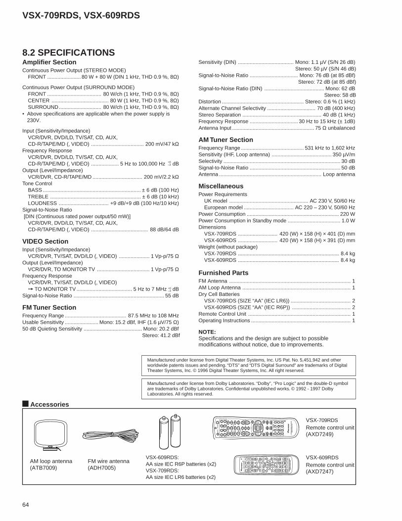
64
VSX-709RDS, VSX-609RDS
8.2 SPECIFICATIONSSensitivity (DIN) ...................................... Mono: 1.1 µV (S/N 26 dB)
Stereo: 50 µV (S/N 46 dB)Signal-to-Noise Ratio ................................. Mono: 76 dB (at 85 dBf)
Stereo: 72 dB (at 85 dBf)Signal-to-Noise Ratio (DIN) ......................................... Mono: 62 dB
Stereo: 58 dBDistortion ........................................................ Stereo: 0.6 % (1 kHz)Alternate Channel Selectivity ................................. 70 dB (400 kHz)Stereo Separation ...................................................... 40 dB (1 kHz)Frequency Response ................................. 30 Hz to 15 kHz (± 1dB)Antenna Input ........................................................ 75 Ω unbalanced
AM Tuner SectionFrequency Range ........................................... 531 kHz to 1,602 kHzSensitivity (IHF, Loop antenna) ......................................... 350 µV/mSelectivity ................................................................................ 30 dBSignal-to-Noise Ratio .............................................................. 50 dBAntenna ...................................................................... Loop antenna
MiscellaneousPower Requirements
UK model ...................................................... AC 230 V, 50/60 HzEuropean model .................................. AC 220 – 230 V, 50/60 Hz
Power Consumption ............................................................... 220 WPower Consumption in Standby mode .................................... 1.0 WDimensions
VSX-709RDS ........................... 420 (W) × 158 (H) × 401 (D) mmVSX-609RDS ........................... 420 (W) × 158 (H) × 391 (D) mm
Weight (without package)VSX-709RDS ..................................................................... 8.4 kgVSX-609RDS ..................................................................... 8.4 kg
Furnished PartsFM Antenna ................................................................................... 1AM Loop Antenna .......................................................................... 1Dry Cell Batteries
VSX-709RDS (SIZE “AA” (IEC LR6)) ......................................... 2VSX-609RDS (SIZE “AA” (IEC R6P)) ........................................ 2
Remote Control Unit ...................................................................... 1Operating Instructions .................................................................... 1
NOTE:Specifications and the design are subject to possiblemodifications without notice, due to improvements.
AM loop antenna(ATB7009)
FM wire antenna(ADH7005)
VSX-609RDS:AA size IEC R6P batteries (x2)VSX-709RDS:AA size IEC LR6 batteries (x2)
VSX-609RDS
VSX-709RDS
SO
UR
CE
MID
NIG
HT
SIG
NA
L S
ELE
CT
TV C
ON
TRO
L
TV V
OL
TVFU
NC
TV
ME
NU
EN
TER
D.A
CC
ES
SB
AN
DC
LAS
S
CH
SE
LEC
TC
H L
EV
EL
AV
PR
E-P
RO
GR
AM
ME
D A
ND
LE
AR
NIN
GR
EM
OTE
CO
NTR
OL
UN
IT
DS
PTE
ST
TON
E FL D
IMM
ER
LOU
DN
ESS
FUN
CTI
ON
SE
TUP
MU
TIN
G
MP
XD
ISP
LAY
RF
ATT
FQ FQ
ST
ST
CH
AN
NE
LEFF
EC
T
MA
STER
VO
LUM
E
DIS
C+1
0
5.1C
H
MU
LTI C
ON
TRO
L
ATT
DV
DTV
VC
RC
D-R
RC
VC
DTU
NTV
C
RE
CE
IVE
R
12
3
45
6
78
9
74
¢
3
1
¡
0
8 2
Î
MU
LTI C
ON
TRO
LD
VD
/LD
TV
/SAT
VC
R/D
VR
C
D
SO
UC
E
CLA
SS
MP
X
B
AN
D
LOUD
NESS
FUN
CTIO
N M
UTIN
G
RECE
IVER
D.AC
CES
S
ATT
VOL
MEN
UTO
PM
ENU
VOL
CH
2
DSP
MO
DE M
IDNI
GHT
5.
1CH
CD
-R/
TAP
E/M
D
CH
AN
NEL
SELE
CT
CH
AN
NEL
LEVE
LEF
FEC
T ENTE
R
ENTE
R
FQ FQ
STST
FLD
IMM
ERRE
MOT
ESE
TUP
MA
STE
RVO
LUM
E
AUD
IO/V
IDEO
PR
E-PR
OG
RA
MM
EDR
EMO
TE C
ON
TRO
L U
NIT
TV C
ON
TRO
L
FUN
C
10
DIS
C
SIG
NA
LSE
LEC
TTE
STTO
NE
RECE
IVER
TU
NE
R
TV C
ONT
Î
12
34
1
¡
4
¢
78
3
56
78
90
‡ CH
AN
NEL
DIS
PLAY
RF
ATT
Accessories
Manufactured under license from Digital Theater Systems, Inc. US Pat. No. 5,451,942 and otherworldwide patents issues and pending. “DTS” and “DTS Digital Surround” are trademarks of DigitalTheater Systems, Inc. © 1996 Digital Theater Systems, Inc. All right reserved.
Manufactured under license from Dolby Laboratories. “Dolby”, “Pro Logic” and the double-D symbolare trademarks of Dolby Laboratories. Confidential unpublished works. © 1992 - 1997 DolbyLaboratories. All rights reserved.
Remote control unit(AXD7247)
Remote control unit(AXD7249)
Amplifier SectionContinuous Power Output (STEREO MODE)
FRONT ....................... 80 W + 80 W (DIN 1 kHz, THD 0.9 %, 8Ω)
Continuous Power Output (SURROUND MODE)FRONT ..................................... 80 W/ch (1 kHz, THD 0.9 %, 8Ω)CENTER ....................................... 80 W (1 kHz, THD 0.9 %, 8Ω)SURROUND............................. 80 W/ch (1 kHz, THD 0.9 %, 8Ω)
• Above specifications are applicable when the power supply is230V.
Input (Sensitivity/Impedance)VCR/DVR, DVD/LD, TV/SAT, CD, AUX,CD-R/TAPE/MD (, VIDEO) .................................... 200 mV/47 kΩ
Frequency ResponseVCR/DVR, DVD/LD, TV/SAT, CD, AUX,CD-R/TAPE/MD (, VIDEO) ................... 5 Hz to 100,000 Hz dB
Output (Level/Impedance)VCR/DVR, CD-R/TAPE/MD .................................. 200 mV/2.2 kΩ
Tone ControlBASS ................................................................... ± 6 dB (100 Hz)TREBLE .............................................................. ± 6 dB (10 kHz)LOUDNESS .................................. +9 dB/+9 dB (100 Hz/10 kHz)
Signal-to-Noise Ratio [DIN (Continuous rated power output/50 mW)]
VCR/DVR, DVD/LD, TV/SAT, CD, AUX,CD-R/TAPE/MD (, VIDEO) ....................................... 88 dB/64 dB
VIDEO SectionInput (Sensitivity/Impedance)
VCR/DVR, TV/SAT, DVD/LD (, VIDEO) ..................... 1 Vp-p/75 ΩOutput (Level/Impedance)
VCR/DVR, TO MONITOR TV .................................... 1 Vp-p/75 ΩFrequency Response
VCR/DVR, TV/SAT, DVD/LD (, VIDEO)= TO MONITOR TV...................................... 5 Hz to 7 MHz dB
Signal-to-Noise Ratio .............................................................. 55 dB
FM Tuner SectionFrequency Range .......................................... 87.5 MHz to 108 MHzUsable Sensitivity ....................... Mono: 15.2 dBf, IHF (1.6 µV/75 Ω)50 dB Quieting Sensitivity ........................................ Mono: 20.2 dBf
Stereo: 41.2 dBf
+0–3
+0–3