Volume 1: Design and Synthesis - Altera
1063
Quartus II Handbook Volume 1: Design and Synthesis Subscribe Send Feedback QII5V1 2015.05.04 101 Innovation Drive San Jose, CA 95134 www.altera.com
Transcript of Volume 1: Design and Synthesis - Altera

Quartus II Handbook Volume 1: Design and Synthesis
Subscribe
Send Feedback
QII5V12015.05.04
101 Innovation DriveSan Jose, CA 95134www.altera.com

Managing Quartus II Projects 12015.05.04
QII5V1 Subscribe Send Feedback
The Quartus II software organizes and manages the elements of your design within a project. The projectencapsulates information about your design hierarchy, libraries, constraints, and project settings. ClickFile > New Project Wizard to quickly create a new project and specify basic project settings
When you open a project, a unified GUI displays integrated project information. The Project Navigatorallows you to view and edit the elements of your project. The Messages window lists important informa‐tion about project processing.
You can save multiple revisions of your project to experiment with settings that achieve your design goals.Quartus II projects support team-based, distributed work flows and a scripting interface.
Quick StartTo quickly create a project and specify basic settings, click File > New Project Wizard.
New Project Wizard
© 2015 Altera Corporation. All rights reserved. ALTERA, ARRIA, CYCLONE, ENPIRION, MAX, MEGACORE, NIOS, QUARTUS and STRATIX words and logos aretrademarks of Altera Corporation and registered in the U.S. Patent and Trademark Office and in other countries. All other words and logos identified astrademarks or service marks are the property of their respective holders as described at www.altera.com/common/legal.html. Altera warrants performanceof its semiconductor products to current specifications in accordance with Altera's standard warranty, but reserves the right to make changes to anyproducts and services at any time without notice. Altera assumes no responsibility or liability arising out of the application or use of any information,product, or service described herein except as expressly agreed to in writing by Altera. Altera customers are advised to obtain the latest version of devicespecifications before relying on any published information and before placing orders for products or services.
ISO9001:2008Registered
www.altera.com101 Innovation Drive, San Jose, CA 95134

Note: The New Project Wizard offers project templates based on fully functioning design examples.Select the Project template option to choose a project template that is ready to compile. Alteraprovides additional project templates as available.
Understanding Quartus II ProjectsA single Quartus II Project File (.qpf) represents each project. The text-based . qpf references the QuartusII Settings File (.qsf), that lists all project files and stores project and entity settings. When you makeproject changes in the GUI, these text files automatically store the changes. The GUI helps to manage:
• Design, EDA, IP core, and Qsys system files• Project settings and constraint files• Project archive and migration files
Table 1-1: Quartus II Project Files
File Type Contains To Edit Format
Project file Project and revision name File > New ProjectWizard
Quartus II Project File (.qpf)
Projectsettings
Lists design files, entitysettings, target device,synthesis directives,placement constraints
Assignments > Settings Quartus II Settings File (.qsf)
Projectdatabase
Compilation results Project > ExportDatabase
Exported Partition File (.qxp)
Timingconstraints
Clock properties,exceptions, setup/hold
Tools > TimeQuestTiming Analyzer
Synopsys Design Constraints File(.sdc)
Logic designfiles
RTL and other designsource files
File > New All supported HDL files
Program‐ming files
Device programmingimage and information
Tools > Programmer SRAM Object File (.sof)Programmer Object File (.pof)
Projectlibrary
Project and global libraryinformation
Tools > Options >Libraries
.qsf(project)
quartus2.ini (global)
IP core files IP core logic, synthesis,and simulationinformation
Tools > IP Catalog All supported HDL files
Quartus II IP File (.qip)
Qsys systemfiles
Qsys system and IP corefiles
Tools > Qsys Qsys System File (.qsys)
1-2 Understanding Quartus II ProjectsQII5V1
2015.05.04
Altera Corporation Managing Quartus II Projects
Send Feedback

File Type Contains To Edit Format
EDA toolfiles
Generated for third-partyEDA tools
Tools > Options > EDATool Options
Verilog Output File (.vo)
VHDL Output File (.vho)
Verilog Quartus Mapping File(.vqm)
Archive files Complete project as singlecompressed file
Project > Archive Project Quartus II Archive File (.qar)
Viewing Basic Project InformationView basic information about your project in the Project Navigator, Report panel, and Messages window.View project elements in the Project Navigator ( View > Utility Windows > Project Navigator). TheProject Navigator displays key project information, including design files, IP components, and revisionsof your project. Use the Project Navigator to:
• View and modify the design hierarchy (right-click > Set as Top-Level Entity)• Set the project revision (right-click > Set Current Revision)• View and update logic design files and constraint files (right-click > Open)• Update IP component version information (right-click > Upgrade IP Component)
Figure 1-1: Project Navigator Hierarchy, Files, Revisions, and IP
Viewing Project ReportsThe Report panel (Processing > Compilation Report) displays detailed reports after project processing,including the following:
• Analysis & Synthesis reports• Fitter reports• Timing analysis reports• Power analysis reports• Signal integrity reports
QII5V12015.05.04 Viewing Basic Project Information 1-3
Managing Quartus II Projects Altera Corporation
Send Feedback

Analyze the detailed project information in these reports to determine correct implementation. Right-click report data to locate and edit the source in project files.
Figure 1-2: Report Panel
Related InformationList of Compilation Reports
Viewing Project MessagesThe Messages window (View > Utility Windows > Messages) displays information, warning, and errormessages about Quartus II processes. Right-click messages to locate the source or get message help.
• Processing tab—displays messages from the most recent process• System tab—displays messages unrelated to design processing• Search—locates specific messages
Messages are written to stdout when you use command-line executables.
Figure 1-3: Messages Window
1-4 Viewing Project MessagesQII5V1
2015.05.04
Altera Corporation Managing Quartus II Projects
Send Feedback

You can suppress display of unimportant messages so they do not obscure valid messages.
Figure 1-4: Message Suppression by Message ID Number
Suppressing MessagesTo supress messages, right-click a message and choose any of the following:
• Suppress Message—suppresses all messages matching exact text• Suppress Messages with Matching ID—suppresses all messages matching the message ID number,
ignoring variables• Suppress Messages with Matching Keyword—suppresses all messages matching keyword or
hierarchy
Message Suppression Guidelines
• You cannot suppress error or Altera legal agreement messages.• Suppressing a message also suppresses any submessages.• Message suppression is revision-specific. Derivative revisions inherit any suppression.• You cannot edit messages or suppression rules during compilation.
Managing Project SettingsThe New Project Wizard helps you initially assign basic project settings. Optimizing project settingsenables the Compiler to generate programming files that meet or exceed your specifications.
The .qsf stores each revision’s project settings.
QII5V12015.05.04 Suppressing Messages 1-5
Managing Quartus II Projects Altera Corporation
Send Feedback

Click Assignments > Settings to access global project settings, including:
• Project files list• Synthesis directives and constraints• Logic options and compiler effort levels• Placement constraints• Timing constraint files• Operating temperature limits and conditions• File generation for other EDA tools• Target device (click Assignments > Device)
The Quartus II Default Settings File (<revision name>_assignment_defaults.qdf) stores initial settingsand constraints for each new project revision.
Figure 1-5: Settings Dialog Box for Global Project Settings
The Assignment Editor (Tools > Assignment Editor) provides a spreadsheet-like interface for assigningall instance-specific settings and constraints.
1-6 Managing Project SettingsQII5V1
2015.05.04
Altera Corporation Managing Quartus II Projects
Send Feedback

Figure 1-6: Assignment Editor Spreadsheet
Optimizing Project SettingsOptimize project settings to meet your design goals. The Quartus II Design Space Explorer II iterativelycompiles your project with various setting combinations to find the optimal setting for your goals.Alternatively, you can create a project revision or project copy to manually compare various projectsettings and design combinations.
Optimizing with Design Space Explorer IIUse Design Space Explorer II (Tools > Launch Design Space Explorer II) to find optimal project settingsfor resource, performance, or power optimization goals. Design Space Explorer II (DSE II) processes yourdesign using various setting and constraint combinations, and reports the best settings for your design.
DSE II attempts multiple seeds to identify one meeting your requirements. DSE II can run differentcompilations on multiple computers in parallel to streamline timing closure.
QII5V12015.05.04 Optimizing Project Settings 1-7
Managing Quartus II Projects Altera Corporation
Send Feedback

Figure 1-7: Design Space Explorer II
Optimizing with Project RevisionsYou can save multiple, named project revisions within your Quartus II project (Project > Revisions).
Each revision captures a unique set of project settings and constraints, but does not capture any logicdesign file changes. Use revisions to experiment with different settings while preserving the original.Youcan compare revisions to determine the best combination, or optimize different revisions for variousapplications. Use revisions for the following:
• Create a unique revision to optimize a design for different criteria, such as by area in one revision andby fMAX in another revision.
• When you create a new revision the default Quartus II settings initially apply.• Create a revision of a revision to experiment with settings and constraints. The child revision includes
all the assignments and settings of the parent revision.
You create, delete, specify current, and compare revisions in the Revisions dialog box. Each time youcreate a new project revision, the Quartus II software creates a new .qsf using the revision name.
To compare each revision’s synthesis, fitting, and timing analysis results side-by-side, click Project >Revisions and then click Compare.
In addition to viewing the compilation results of each revision, you can also compare the assignments foreach revision. This comparison reveals how different optimization options affect your design.
1-8 Optimizing with Project RevisionsQII5V1
2015.05.04
Altera Corporation Managing Quartus II Projects
Send Feedback

Figure 1-8: Comparing Project Revisions
Copying Your ProjectClick Project > Copy Project to create a separate copy of your project, rather than just a revision withinthe same project.
The project copy includes all design files, .qsf(s), and project revisions. Use this technique to optimizeproject copies for different applications. For example, optimize one project to interface with a 32-bit databus, and optimize a project copy to interface with a 64-bit data bus.
Managing Logic Design FilesThe Quartus II software helps you create and manage the logic design files in your project. Logic designfiles contain the logic that implements your design. When you add a logic design file to the project, theCompiler automatically compiles that file as part of the project. The Compiler synthesizes your logicdesign files to generate programming files for your target device.
The Quartus II software includes full-featured schematic and text editors, as well as HDL templates toaccelerate your design work. The Quartus II software supports VHDL Design Files (.vhd), Verilog HDLDesign Files (.v), SystemVerilog (. sv) and schematic Block Design Files (. bdf). The Quartus II softwarealso supports Verilog Quartus Mapping (.vqm) design files generated by other design entry and synthesistools. In addition, you can combine your logic design files with Altera and third-party IP core design files,including combining components into a Qsys system (. qsys).
The New Project Wizard prompts you to identify logic design files. Add or remove project files by clickingProject > Add/Remove Files in Project. View the project’s logic design files in the Project Navigator.
QII5V12015.05.04 Copying Your Project 1-9
Managing Quartus II Projects Altera Corporation
Send Feedback

Figure 1-9: Design and IP Files in Project Navigator
Right-click files in the Project Navigator to:
• Open and edit the file• Remove File from Project• Set as Top-Level Entity for the project revision• Create a Symbol File for Current File for display in schematic editors• Edit file Properties
Including Design LibrariesYou can include design files libraries in your project. Specify libraries for a single project, or for allQuartus II projects. The.qsf stores project library information.
The quartus2.ini file stores global library information.
Related InformationDesign Library Migration Guidelines on page 1-41
Specifying Design LibrariesTo specify project libraries from the GUI:
1. Click Assignment > Settings.2. Click Libraries andspecify the Project Library name or Global Library name.Alternatively, you can
specify project libraries with SEARCH_PATH in the .qsf, and global libraries in the quartus2.ini file.
Related Information
• Recommended Design Practices on page 11-1• Recommended HDL Coding Styles on page 12-1
Managing Timing ConstraintsView basic information about your project in the Project Navigator, Report panel, and Messages window.
Apply appropriate timing constraints to correctly optimize fitting and analyze timing for your design. TheFitter optimizes the placement of logic in the device to meet your specified timing and routingconstraints.
1-10 Including Design LibrariesQII5V1
2015.05.04
Altera Corporation Managing Quartus II Projects
Send Feedback

Specify timing constraints in the TimeQuest Timing Analyzer (Tools > TimeQuest Timing Analyzer), orin an .sdc file. Specify constraints for clock characteristics, timing exceptions, and external signal setupand hold times before running analysis. TimeQuest reports the detailed information about the perform‐ance of your design compared with constraints in the Compilation Report panel.
Save the constraints you specify in the GUI in an industry-standard Synopsys Design Constraints File(.sdc). You can subsequently edit the text-based .sdc file directly.
Figure 1-10: TimeQuest Timing Analyzer and SDC Syntax Example
Related InformationQuartus II TimeQuest Timing Analyzer
Introduction to Altera IP CoresAltera® and strategic IP partners offer a broad portfolio of off-the-shelf, configurable IP cores optimizedfor Altera devices. The Quartus® II software installation includes the Altera IP library. You can integrateoptimized and verified Altera IP cores into your design to shorten design cycles and maximizeperformance. You can evaluate any Altera IP core in simulation and compilation in the Quartus IIsoftware. The Quartus II software also supports integration of IP cores from other sources. Use the IPCatalog to efficiently parameterize and generate synthesis and simulation files for a custom IP variation.
QII5V12015.05.04 Introduction to Altera IP Cores 1-11
Managing Quartus II Projects Altera Corporation
Send Feedback

The Altera IP library includes the following categories of IP cores:
• Basic functions• DSP functions• Interface protocols• Low power functions• Memory interfaces and controllers• Processors and peripherals
Note: The IP Catalog (Tools > IP Catalog) and parameter editor replace the MegaWizard™ Plug-InManager for IP selection and parameterization, beginning in Quartus II software version 14.0. Usethe IP Catalog and parameter editor to locate and paramaterize Altera and other supported IPcores.
Related Information
• IP User Guide Documentation• Altera IP Release Notes
Installing and Licensing IP CoresThe Altera IP Library provides many useful IP core functions for your production use without purchasingan additional license. Some Altera MegaCore® IP functions require that you purchase a separate licensefor production use. However, the OpenCore® feature allows evaluation of any Altera IP core in simulationand compilation in the Quartus II software. After you are satisfied with functionality and perfformance,visit the Self Service Licensing Center to obtain a license number for any Altera product.
Figure 1-11: IP Core Installation Path
acds
quartus - Contains the Quartus II softwareip - Contains the Altera IP Library and third-party IP cores
altera - Contains the Altera IP Library source code<IP core name> - Contains the IP core source files
Note: The default IP installation directory on Windows is <drive>:\altera\<version number>; on Linux it is<home directory>/altera/ <version number>.
Related Information
• Altera Licensing Site• Altera Software Installation and Licensing Manual
OpenCore Plus IP EvaluationAltera's free OpenCore Plus feature allows you to evaluate licensed MegaCore IP cores in simulation andhardware before purchase. You need only purchase a license for MegaCore IP cores if you decide to takeyour design to production. OpenCore Plus supports the following evaluations:
1-12 Installing and Licensing IP CoresQII5V1
2015.05.04
Altera Corporation Managing Quartus II Projects
Send Feedback

• Simulate the behavior of a licensed IP core in your system.• Verify the functionality, size, and speed of the IP core quickly and easily.• Generate time-limited device programming files for designs that include IP cores.• Program a device with your IP core and verify your design in hardware.
OpenCore Plus evaluation supports the following two operation modes:
• Untethered—run the design containing the licensed IP for a limited time.• Tethered—run the design containing the licensed IP for a longer time or indefinitely. This requires a
connection between your board and the host computer.
Note: All IP cores that use OpenCore Plus time out simultaneously when any IP core in the design timesout.
IP Catalog and Parameter EditorThe Quartus II IP Catalog (Tools > IP Catalog) and parameter editor help you easily customize andintegrate IP cores into your project. You can use the IP Catalog and parameter editor to select, customize,and generate files representing your custom IP variation.
Note: The IP Catalog (Tools > IP Catalog) and parameter editor replace the MegaWizard™ Plug-InManager for IP selection and parameterization, beginning in Quartus II software version 14.0. Usethe IP Catalog and parameter editor to locate and paramaterize Altera IP cores.
The IP Catalog lists installed IP cores available for your design. Double-click any IP core to launch theparameter editor and generate files representing your IP variation. The parameter editor prompts you tospecify an IP variation name, optional ports, and output file generation options. The parameter editorgenerates a top-level Qsys system file (.qsys) or Quartus II IP file (.qip) representing the IP core in yourproject. You can also parameterize an IP variation without an open project.
Use the following features to help you quickly locate and select an IP core:
• Filter IP Catalog to Show IP for active device family or Show IP for all device families. If you have noproject open, select the Device Family in IP Catalog.
• Type in the Search field to locate any full or partial IP core name in IP Catalog.• Right-click an IP core name in IP Catalog to display details about supported devices, open the IP core's
installation folder, and view links to documentation.• Click Search for Partner IP, to access partner IP information on the Altera website.
QII5V12015.05.04 IP Catalog and Parameter Editor 1-13
Managing Quartus II Projects Altera Corporation
Send Feedback

Figure 1-12: Quartus II IP Catalog
Search for installed IP cores
Double-click to customize, right-click for detailed information
Show IP only for target device
Note: The IP Catalog is also available in Qsys (View > IP Catalog). The Qsys IP Catalog includesexclusive system interconnect, video and image processing, and other system-level IP that are notavailable in the Quartus II IP Catalog. For more information about using the Qsys IP Catalog, referto Creating a System with Qsys in the Quartus II Handbook.
Related InformationCreating a System With Qsys on page 5-1
Using the Parameter EditorThe parameter editor helps you to configure IP core ports, parameters, and output file generation options.
• Use preset settings in the parameter editor (where provided) to instantly apply preset parameter valuesfor specific applications.
• View port and parameter descriptions, and links to documentation.• Generate testbench systems or example designs (where provided).
1-14 Using the Parameter EditorQII5V1
2015.05.04
Altera Corporation Managing Quartus II Projects
Send Feedback

Figure 1-13: IP Parameter Editors
View IP portand parameter details
Apply preset parameters forspecific applications
Specify your IP variationname and target device
Legacy parameter editors
Adding IP Cores to IP CatalogThe IP Catalog automatically displays Altera IP cores found in the project directory, in the Alterainstallation directory, and in the defined IP search path. The IP Catalog can include Altera-provided IPcomponents, third-party IP components, custom IP components that you provide, and previouslygenerated Qsys systems.
You can use the IP Search Path option (Tools > Options) to include custom and third-party IPcomponents in the IP Catalog. The IP Catalog displays all IP cores in the IP search path. The Quartus IIsoftware searches the directories listed in the IP search path for the following IP core files:
• Component Description File (_hw.tcl)—Defines a single IP core.• IP Index File (.ipx)—Each .ipx file indexes a collection of available IP cores, or a reference to other
directories to search. In general, .ipx files facilitate faster searches.
The Quartus II software searches some directories recursively and other directories only to a specificdepth. When the search is recursive, the search stops at any directory that contains an _hw.tcl or .ipx file.
In the following list of search locations, a recursive descent is annotated by **. A single * signifies any file.
Table 1-2: IP Search Locations
Location Description
PROJECT_DIR/* Finds IP components and index files in the Quartus II projectdirectory.
PROJECT_DIR/ip/**/* Finds IP components and index files in any subdirectory of the /ipsubdirectory of the Quartus II project directory.
QII5V12015.05.04 Adding IP Cores to IP Catalog 1-15
Managing Quartus II Projects Altera Corporation
Send Feedback

Figure 1-14: Specifying IP Search Locations
Adds new global IP search paths
Changes search path order
Adds new project-specific IP search paths
Lists current project and global search paths
If the Quartus II software recognizes two IP cores with the same name, the following search pathprecedence rules determine the resolution of files:
1. Project directory.2. Project database directory.3. Project IP search path specified in IP Search Locations, or with the SEARCH_PATH assignment in the
Quartus II Settings File (.qsf) for the current project revision.4. Global IP search path specified in IP Search Locations, or with the SEARCH_PATH assignment in the
quartus2.ini file.5. Quartus software libraries directory, such as <Quartus Installation>\libraries.
Note: If you add a component to the search path, you must refresh your system by clicking File > Refreshto update the IP Catalog.
General Settings for IPYou can use the following settings to control how the Quartus II software manages IP cores in yourproject.
1-16 General Settings for IPQII5V1
2015.05.04
Altera Corporation Managing Quartus II Projects
Send Feedback

Table 1-3: IP Core General Setting Locations
Setting Location Description
Tools > Options > IPSettings
Or
Assignments > Settings >IP Settings (only enabledwith open project)
• Specify your IP generation HDL preference. The parameter editorgenerates IP files in your preferred HDL by default.
• Increase Maximum Qsys memory usage size if you experience slowprocessing for large systems, or if Qsys reports an Out of Memory error.
• Specify whether to Automatically add Quartus II IP files to all projects.Disable this option to control addition of IP files manually. You maywant to experiment with IP before adding to a project.
• Use the IP Regeneration Policy setting to control when synthesis filesare regenerated for each IP variation. Typically you Always regeneratesynthesis files for IP cores after making changes to an IP variation.
Tools > Options > IPCatalog Search Locations
Or
Assignments > Settings >IP Catalog SearchLocations
• Specify project and global IP search locations. The Quartus II softwaresearches for IP cores in the project directory, in the Altera installationdirectory, and in the IP search path.
Assignments > Settings >Simulation
• NativeLink Settings allow you to automatically compile testbenches forsupported simulators. You can also specify a script to compile thetestbench, and a script to set up the simulation.
Specifying IP Core Parameters and OptionsYou can quickly configure a custom IP variation in the parameter editor. Use the following steps tospecify IP core options and parameters in the parameter editor. Refer to Specifying IP Core Parametersand Options (Legacy Parameter Editors) for configuration of IP cores using the legacy parameter editor.
1. In the IP Catalog (Tools > IP Catalog), locate and double-click the name of the IP core to customize.The parameter editor appears.
2. Specify a top-level name for your custom IP variation. The parameter editor saves the IP variationsettings in a file named <your_ip>.qsys. Click OK.
3. Specify the parameters and options for your IP variation in the parameter editor, including one ormore of the following. Refer to your IP core user guide for information about specific IP coreparameters.
• Optionally select preset parameter values if provided for your IP core. Presets specify initialparameter values for specific applications.
• Specify parameters defining the IP core functionality, port configurations, and device-specificfeatures.
• Specify options for processing the IP core files in other EDA tools.4. Click Generate HDL, the Generation dialog box appears.5. Specify output file generation options, and then click Generate. The IP variation files generate
according to your specifications.
QII5V12015.05.04 Specifying IP Core Parameters and Options 1-17
Managing Quartus II Projects Altera Corporation
Send Feedback

6. To generate a simulation testbench, click Generate > Generate Testbench System.7. To generate an HDL instantiation template that you can copy and paste into your text editor, click
Generate > HDL Example.8. Click Finish. The parameter editor adds the top-level .qsys file to the current project automatically. If
you are prompted to manually add the .qsys file to the project, click Project > Add/Remove Files inProject to add the file.
9. After generating and instantiating your IP variation, make appropriate pin assignments to connectports.
Figure 1-15: IP Parameter Editor
View IP portand parameter details
Apply preset parameters forspecific applications
Specify your IP variation nameand target device
Files Generated for Altera IP CoresThe Quartus II software generates the following IP core output file structure:
1-18 Files Generated for Altera IP CoresQII5V1
2015.05.04
Altera Corporation Managing Quartus II Projects
Send Feedback

Figure 1-16: IP Core Generated Files
<your_testbench>_tb.csv
<your_testbench>_tb.spd
<your_ip>.cmp - VHDL component declaration file
<your_ip>.ppf - XML I/O pin information file
<your_ip>.qip - Lists IP synthesis files
<your_ip>.sip - Contains assingments for IP simulation files
<your_ip>.v or .vhdTop-level IP synthesis file
<your_ip>.v or .vhdTop-level simulation file
<simulator_setup_scripts>
<your_ip>.qsys - System or IP integration file
<your_ip>_bb.v - Verilog HDL black box EDA synthesis file
<your_ip>_inst.v or .vhd - Sample instantiation template
<your_ip>_generation.rpt - IP generation report
<your_ip>.debuginfo - Contains post-generation information
<your_ip>.html - Connection and memory map data
<your_ip>.bsf - Block symbol schematic
<your_ip>.spd - Combines simulation scripts for multiple cores
<your_ip>_tb.qsysTestbench system file
<your_ip>.sopcinfo - Software tool-chain integration file
<project directory>
<EDA tool setupscripts>
<your_ip>
IP variation files<testbench>_tb
testbench system
sim
Simulation files
synth
IP synthesis files
sim
simulation files
<EDA tool name>Simulator scripts
<testbench>_tb
<ip subcores> nSubcore libraries
simSubcore
Simulation files
synthSubcore
synthesis files
<HDL files><HDL files>
<your_ip> n
IP variation files
testbench files
Table 1-4: IP Core Generated Files
File Name Description
<my_ip>.qsys The Qsys system or top-level IP variation file. <my_ip> is the namethat you give your IP variation.
<system>.sopcinfo Describes the connections and IP component parameterizations inyour Qsys system. You can parse its contents to get requirementswhen you develop software drivers for IP components.
Downstream tools such as the Nios II tool chain use this file.The .sopcinfo file and the system.h file generated for the Nios II toolchain include address map information for each slave relative to eachmaster that accesses the slave. Different masters may have a differentaddress map to access a particular slave component.
QII5V12015.05.04 Files Generated for Altera IP Cores 1-19
Managing Quartus II Projects Altera Corporation
Send Feedback

File Name Description
<my_ip>.cmp The VHDL Component Declaration (.cmp) file is a text file thatcontains local generic and port definitions that you can use in VHDLdesign files.
<my_ip>.html A report that contains connection information, a memory mapshowing the address of each slave with respect to each master towhich it is connected, and parameter assignments.
<my_ip>_generation.rpt IP or Qsys generation log file. A summary of the messages during IPgeneration.
<my_ip>.debuginfo Contains post-generation information. Used to pass System Consoleand Bus Analyzer Toolkit information about the Qsys interconnect.The Bus Analysis Toolkit uses this file to identify debug componentsin the Qsys interconnect.
<my_ip>.qip Contains all the required information about the IP component tointegrate and compile the IP component in the Quartus II software.
<my_ip>.csv Contains information about the upgrade status of the IP component.
<my_ip>.bsf A Block Symbol File (.bsf) representation of the IP variation for usein Quartus II Block Diagram Files (.bdf).
<my_ip>.spd Required input file for ip-make-simscript to generate simulationscripts for supported simulators. The .spd file contains a list of filesgenerated for simulation, along with information about memoriesthat you can initialize.
<my_ip>.ppf The Pin Planner File (.ppf) stores the port and node assignments forIP components created for use with the Pin Planner.
<my_ip>_bb.v You can use the Verilog black-box (_bb.v) file as an empty moduledeclaration for use as a black box.
<my_ip>.sip Contains information required for NativeLink simulation of IPcomponents. You must add the .sip file to your Quartus project.
<my_ip>_inst.v or _inst.vhd HDL example instantiation template. You can copy and paste thecontents of this file into your HDL file to instantiate the IP variation.
<my_ip>.regmap If the IP contains register information, the .regmap file generates.The .regmap file describes the register map information of masterand slave interfaces. This file complements the .sopcinfo file byproviding more detailed register information about the system. Thisenables register display views and user customizable statistics inSystem Console.
1-20 Files Generated for Altera IP CoresQII5V1
2015.05.04
Altera Corporation Managing Quartus II Projects
Send Feedback

File Name Description
<my_ip>.svd Allows HPS System Debug tools to view the register maps ofperipherals connected to HPS within a Qsys system.
During synthesis, the .svd files for slave interfaces visible to SystemConsole masters are stored in the .sof file in the debug section.System Console reads this section, which Qsys can query for registermap information. For system slaves, Qsys can access the registers byname.
<my_ip>.v
or
<my_ip>.vhd
HDL files that instantiate each submodule or child IP core forsynthesis or simulation.
mentor/ Contains a ModelSim® script msim_setup.tcl to set up and run asimulation.
aldec/ Contains a Riviera-PRO script rivierapro_setup.tcl to setup and run asimulation.
/synopsys/vcs
/synopsys/vcsmx
Contains a shell script vcs_setup.sh to set up and run a VCS®
simulation.
Contains a shell script vcsmx_setup.sh and synopsys_ sim.setup file toset up and run a VCS MX® simulation.
/cadence Contains a shell script ncsim_setup.sh and other setup files to set upand run an NCSIM simulation.
/submodules Contains HDL files for the IP core submodule.<child IP cores>/ For each generated child IP core directory, Qsys generates /synth and /
sim sub-directories.
Specifying IP Core Parameters and Options (Legacy Parameter Editors)Some IP cores use a legacy version of the parameter editor for configuration and generation. Use thefollowing steps to configure and generate an IP variation using a legacy parameter editor.
Note: The legacy parameter editor generates a different output file structure than the latest parametereditor. Refer to Specifying IP Core Parameters and Options for configuration of IP cores that use thelatest parameter editor.
QII5V12015.05.04 Specifying IP Core Parameters and Options (Legacy Parameter Editors) 1-21
Managing Quartus II Projects Altera Corporation
Send Feedback

Figure 1-17: Legacy Parameter Editors
Legacy parameter editors
1. In the IP Catalog (Tools > IP Catalog), locate and double-click the name of the IP core to customize.The parameter editor appears.
2. Specify a top-level name and output HDL file type for your IP variation. This name identifies the IPcore variation files in your project. Click OK.
3. Specify the parameters and options for your IP variation in the parameter editor. Refer to your IP coreuser guide for information about specific IP core parameters.
4. Click Finish or Generate (depending on the parameter editor version). The parameter editor generatesthe files for your IP variation according to your specifications. Click Exit if prompted when generationis complete. The parameter editor adds the top-level .qip file to the current project automatically.
Note: To manually add an IP variation generated with legacy parameter editor to a project, clickProject > Add/Remove Files in Project and add the IP variation .qip file.
Files Generated for Altera IP Cores (Legacy Parameter Editors)The Quartus II software generates one of the following output file structures for Altera IP cores that use alegacy parameter editor.
1-22 Files Generated for Altera IP Cores (Legacy Parameter Editors)QII5V1
2015.05.04
Altera Corporation Managing Quartus II Projects
Send Feedback

Figure 1-18: IP Core Generated Files (Legacy Parameter Editor)
Generated IP File Output C Generated IP File Output D
Generated IP File Output B <Project Directory>
<your_ip>.html - IP core generation report
<your_ip>_testbench.v or .vhd - Testbench file1
<your_ip>.bsf - Block symbol schematic file
<your_ip>_syn.v or .vhd - Timing & resource estimation netlist 1
<your_ip>_bb - Verilog HDL black box EDA synthesis file
<your_ip>.vo or .vho - IP functional simulation model 2
<your_ip>.qip - Quartus II IP integration file
<your_ip>.v or .vhd - Top-level HDL IP variation definition
<your_ip>_block_period_stim.txt - Testbench simulation data 1
<your_ip>-library - Contains IP subcomponent synthesis libraries
Generated IP File Output A <Project Directory>
<your_ip>.v or .vhd - Top-level IP synthesis file
<your_ip>_inst.v or .vhd - Sample instantiation template
<your_ip>.bsf - Block symbol schematic file
<your_ip>.vo or .vho - IP functional simulation model 2<your_ip>_syn.v or .vhd - Timing & resource estimation netlist 1
<your_ip>_bb.v - Verilog HDL black box EDA synthesis file
<your_ip>.qip - Quartus II IP integration file
greybox_tmp 3
<your_ip>.cmp - VHDL component declaration file
<Project Directory>
<your_ip>_sim 1
<Altera IP>_instance.vo - IPFS model 2
<simulator_vendor><simulator setup scripts>
<your_ip>.qip - Quartus II IP integration file
<your_ip>.sip - Lists files for simulation
<your_ip>_testbench or _example - Testbench or example1
<your_ip>.v, .sv. or .vhd - Top-level IP synthesis file
<AlteraIP_name>_instance
<your_ip>_syn.v or .vhd - Timing & resource estimation netlist 1<your_ip>.cmp - VHDL component declaration file
<your_ip>.bsf - Block symbol schematic file
<your_ip> - IP core synthesis files
<your_ip>.sv, .v, or .vhd - HDL synthesis files
<your_ip>.sdc - Timing constraints file
<your_ip>.ppf - XML I/O pin information file
<your_ip>.spd - Combines individual simulation scripts 1
<your_ip>_sim.f - Refers to simulation models and scripts 1
<Project Directory>
<your_ip>_bb.v - Verilog HDL black box EDA synthesis file
<your_ip>_inst.v or .vhd - Sample instantiation template
synthesis - IP synthesis files
<your_ip>.qip - Lists files for synthesis
testbench - Simulation testbench files 1
<testbench_hdl_files>
<simulator_vendor> - Testbench for supported simulators
<simulation_testbench_files>
<your_ip>.v or .vhd - Top-level IP variation synthesis file
simulation - IP simulation files<your_ip>.sip - NativeLink simulation integration file
<simulator vendor> - Simulator setup scripts<simulator_setup_scripts>
<your_ip> - IP core variation files
<your_ip>.qip or .qsys - System or IP integration file
<your_ip>_generation.rpt - IP generation report
<your_ip>.bsf - Block symbol schematic file
<your_ip>.ppf - XML I/O pin information file
<your_ip>.spd - Combines individual simulation startup scripts 1
<your_ip>.html - Contains memory map
<your_ip>.sopcinfo - Software tool-chain integration file
<your_ip>_syn.v or .vhd - Timing & resource estimation netlist 1
<your_ip>.debuginfo - Lists files for synthesis
<your_ip>.v, .vhd, .vo, .vho - HDL or IPFS models2
<your_ip>_tb - Testbench for supported simulators<your_ip>_tb.v or .vhd - Top-level HDL testbench file
Notes:1. If supported and enabled for your IP variation2. If functional simulation models are generated3. Ignore this directory
Note: To manually add an IP variation to a Quartus II project, click Project > Add/Remove Files inProject and add only the IP variation .qip or .qsys file, but not both, to the project. Do notmanually add the top-level HDL file to the project.
Scripting IP Core GenerationYou can alternatively use command-line utilities to define and generate an IP core variation outside of theQuartus II GUI.Use qsys-script to run a Tcl file that parameterizes an IP variation you define in ascript. Then, use qsys-generate to generate a .qsys file representing your parameterized IP variation.
QII5V12015.05.04 Scripting IP Core Generation 1-23
Managing Quartus II Projects Altera Corporation
Send Feedback

The qsys-generate command is the same as when generating using the Qsys GUI. For command-linehelp listing all options for these executables, type <executable name> --help
To create a instance of a parameterizable Altera IP core at the command line, rather than using the GUI,follow these steps:
1. Run qsys-script to execute a Tcl script, similar to the example, that instantiates the IP and sets the IPparameters defined by the script:
qsys-script --script=<script_file>.tcl
2. Run qsys-generate to generate the RTL for the IP variation:
qsys-generate <IP variation file>.qsys
Note: Creating an IP generation script is an advanced feature that requires access to special IP coreparameters. For more information about creating an IP generation script, contact your Altera salesrepresentative.
Table 1-5: qsys-generate Command-Line Options
Option Usage Description
<1st arg file> Required The name of the .qsys system file togenerate.
--synthesis=<VERILOG|VHDL> Optional Creates synthesis HDL files that Qsys usesto compile the system in a Quartus IIproject. You must specify the preferredgeneration language for the top-level RTLfile for the generated Qsys system.
--block-symbol-file Optional Creates a Block Symbol File (.bsf) for theQsys system.
--simulation=<VERILOG|VHDL> Optional Creates a simulation model for the Qsyssystem. The simulation model containsgenerated HDL files for the simulator, andmay include simulation-only features. Youmust specify the preferred simulationlanguage.
--testbench=<SIMPLE|STANDARD> Optional Creates a testbench system that instantiatesthe original system, adding bus functionalmodels (BFMs) to drive the top-levelinterfaces. When you generate the system,the BFMs interact with the system in thesimulator.
--testbench-simulation=<VERILOG|VHDL> Optional After you create the testbench system, youcan create a simulation model for thetestbench system.
1-24 Scripting IP Core GenerationQII5V1
2015.05.04
Altera Corporation Managing Quartus II Projects
Send Feedback

Option Usage Description
--search-path=<value> Optional If you omit this command, Qsys uses astandard default path. If you provide thiscommand, Qsys searches a comma-separated list of paths. To include thestandard path in your replacement, use "$",for example, "/extra/dir,$".
--jvm-max-heap-size=<value> Optional The maximum memory size that Qsys usesfor allocations when running qsys-generate. You specify the value as <size><unit>, where unit is m (or M) formultiples of megabytes or g (or G) formultiples of gigabytes. The default value is512m.
--family=<value> Optional Specifies the device family.
--part=<value> Optional Specifies the device part number. If set, thisoption overrides the --family option.
--allow-mixed-language-simulation Optional Enables a mixed language simulationmodel generation. If true, if a preferredsimulation language is set, Qsys uses afileset of the component for thesimulation model generation. When false,which is the default, Qsys uses thelanguage specified with --file-set=<value> for all components forsimulation model generation. The currentversion of the ModelSim-Altera simulatorsupports mixed language simulation.
Modifying an IP VariationYou can easily modify the parameters of any Altera IP core variation in the parameter editor to matchyour design requirements. Use any of the following methods to modify an IP variation in the parametereditor.
Table 1-6: Modifying an IP Variation
Menu Command Action
File > Open Select the top-level HDL (.v, or .vhd) IP variation file tolaunch the parameter editor and modify the IP variation.Regenerate the IP variation to implement your changes.
View > Utility Windows > ProjectNavigator > IP Components
Double-click the IP variation to launch the parametereditor and modify the IP variation. Regenerate the IPvariation to implement your changes.
QII5V12015.05.04 Modifying an IP Variation 1-25
Managing Quartus II Projects Altera Corporation
Send Feedback

Menu Command Action
Project > Upgrade IP Components Select the IP variation and click Upgrade in Editor tolaunch the parameter editor and modify the IP variation.Regenerate the IP variation to implement your changes.
Upgrading IP CoresIP core variants generated with a previous version of the Quartus II software may require upgradingbefore use in the current version of the Quartus II software. Click Project > Upgrade IP Components toidentify and upgrade outdated IP core variants.
Icons in the Upgrade IP Components dialog box indicate when IP upgrade is required, optional, orunsupported for IP cores in your design. This dialog box may open automatically when you open aproject containing upgradeable IP variations. You must upgrade IP cores that require upgrade before youcan compile the IP variation in the current version of the Quartus II software.
The upgrade process preserves the original IP variation file in the project directory as <my_variant>_BAK.qsys for IP targeting Arria 10 and later devices, and as <my_variant>_BAK.v, .sv, or .vhd for legacy IPtargeting 28nm devices and greater.
Note: Upgrading IP cores for Arria 10 and later devices may append a unique identifier to the original IPcore entity name(s), without similarly modifying the IP instance name. There is no requirement toupdate these entity references in any supporting Quartus II file; such as the Quartus II Settings File(.qsf), Synopsys Design Constraints File (.sdc), or SignalTap File (.stp), if these files contain instancenames. The Quartus II software reads only the instance name and ignores the entity name in pathsthat specify both names. Use only instance names in assignments.
Table 1-7: IP Core Upgrade Status
IP Core Status Description
IP Upgraded
Your IP variation uses the lastest version of the IP core.
IP Upgrade Optional
Upgrade is optional for this IP variation in the current version of the QuartusII software. You can upgrade this IP variation to take advantage of the latestdevelopment of this IP core. Alternatively you can retain previous IP corecharacteristics by declining to upgrade. Refer to the Description for detailsabout IP core version differences. If you do not upgrade the IP, the IP variationsynthesis and simulation files are unchanged and you cannot modifyparameters until upgrading.
IP Upgrade MismatchWarning
Warning of non-critical IP core differences in migrating IP to another devicefamily.
1-26 Upgrading IP CoresQII5V1
2015.05.04
Altera Corporation Managing Quartus II Projects
Send Feedback

IP Core Status Description
IP Upgrade Required
You must upgrade the IP variation before compiling in the current version ofthe Quartus II software. Refer to the Description for details about IP coreversion differences.
IP Upgrade Unspported
Upgrade of the IP variation is not supported in the current version of theQuartus II software due to incompatibility with the current version of theQuartus II software. You are prompted to replace the unsupported IP corewith a supported equivalent IP core from the IP Catalog. Refer to the Descrip‐tion for details about IP core version differences and links to Release Notes.
IP End of Life
Altera designates the IP core as end-of-life status. You may or may not be ableto edit the IP core in the parameter editor. Support for this IP corediscontinues in future releases of the Quartus II software.
Encrypted IP Core
The IP variation is encrypted.
Follow these steps to upgrade IP cores:
1. In the latest version of the Quartus II software, open the Quartus II project containing an outdated IPcore variation. The Upgrade IP Components dialog automatically displays the status of IP cores inyour project, along with instructions for upgrading each core. Click Project > Upgrade IPComponents to access this dialog box manually.
2. To upgrade one or more IP cores that support automatic upgrade, ensure that the Auto Upgradeoption is turned on for the IP core(s), and then click Perform Automatic Upgrade. The Status andVersion columns update when upgrade is complete. Example designs provided with any Altera IP coreregenerate automatically whenever you upgrade an IP core.
3. To manually upgrade an individual IP core, select the IP core and then click Upgrade in Editor (orsimply double-click the IP core name. The parameter editor opens, allowing you to adjust parametersand regenerate the latest version of the IP core.
QII5V12015.05.04 Upgrading IP Cores 1-27
Managing Quartus II Projects Altera Corporation
Send Feedback

Figure 1-19: Upgrading IP Cores
Runs “Auto Upgrade” on all supported outdated coresOpens editor for manual IP upgrade
“Auto Upgrade”supported
Upgrade required
Upgradeoptional
Upgrade details
“Auto Upgrade”successful
Note: IP cores older than Quartus II software version 12.0 do not support upgrade. Altera verifies thatthe current version of the Quartus II software compiles the previous version of each IP core.The Altera IP Release Notes reports any verification exceptions for Altera IP cores. Altera doesnot verify compilation for IP cores older than the previous two releases.
Related InformationAltera IP Release Notes
Migrating IP Cores to a Different DeviceIP migration allows you to target the latest device families with IP originally generated for a differentdevice. Some Altera IP cores migrate automatically, some IP cores require manual IP regeneration, andsome do not support device migration and must be replaced in your design.The text and icons in the Upgrade IP Components dialog box identifies the migration support for eachIP core in the design.
Note: Migration of some IP cores requires installed support for the original and migration devicefamilies. For example, migration from a Stratix V device to an Arria 10 device requires installationof Stratix V and Arria 10 device families with the Quartus II software.
1-28 Migrating IP Cores to a Different DeviceQII5V1
2015.05.04
Altera Corporation Managing Quartus II Projects
Send Feedback

Figure 1-20: Upgrading IP Cores
Double-click to upgrade in editor(no auto upgrade)
Upgrade required
Migration details
Supports Auto upgrade
Upgrade success
1. Click File > Open Project and open the Quartus II project containing IP for migration to anotherdevice in the original version of the Quartus II software.
2. To specify a different target device for migration, click Assignments > Device and select the targetdevice family.
3. To display IP cores requiring migration, click Project > Upgrade IP Components. The Descriptionfield prompts you to run auto update or double-click IP cores for migration.
4. To migrate one or more IP cores that support automatic upgrade, ensure that the Auto Upgradeoption is turned on for the IP core(s), and then click Perform Automatic Upgrade. The Status andVersion columns update when upgrade is complete.
5. To migrate an IP core that does not support automatic upgrade, double-click the IP core name, andthen click OK. The parameter editor appears.a. If the parameter editor specifies a Currently selected device family, turn off Match project/
default, and then select the new target device family.b. Click Finish to migrate the IP variation using best-effort mapping to new parameters and settings.
A new parameter editor opens displaying best-effort mapped parameters.c. Click Generate HDL, and then confirm the Synthesis and Simulation file options. Verilog HDL is
the defauilt output file format specified. If your original IP core was generated for VHDL, selectVHDL to retain the original output format.
QII5V12015.05.04 Migrating IP Cores to a Different Device 1-29
Managing Quartus II Projects Altera Corporation
Send Feedback

6. To regenerate the new IP variation for the new target device, click Generate. When generation iscomplete, click Close.
7. Click Finish to complete migration of the IP core. Click OK if you are prompted to overwrite IP corefiles. The Device Family column displays the new target device name when migration is complete. Themigration process replaces <my_ip>.qip with the <my_ip>.qsys top-level IP file in your project.
Note: If migration does not replace <my_ip>.qip with <my_ip>.qsys, click Project > Add/RemoveFiles in Project to replace the file in your project.
8. Review the latest parameters in the parameter editor or generated HDL for correctness. IP migrationmay change ports, parameters, or functionality of the IP core. During migration, the IP core's HDLgenerates into a library that is different from the original output location of the IP core. Update anyassignments that reference outdated locations. If your upgraded IP core is represented by a symbol in asupporting Block Design File schematic, replace the symbol with the newly generated <my_ip>.bsfafter migration.
Note: The migration process may change the IP variation interface, parameters, and functionality.This may require you to change your design or to re-parameterize your variant after theUpgrade IP Components dialog box indicates that migration is complete. The Descriptionfield identifies IP cores that require design or parameter changes.
Related InformationAltera IP Release Notes
Simulating Altera IP Cores in other EDA ToolsThe Quartus II software supports RTL and gate-level design simulation of Altera IP cores in supportedEDA simulators. Simulation involves setting up your simulator working environment, compilingsimulation model libraries, and running your simulation.
You can use the functional simulation model and the testbench or example design generated with your IPcore for simulation. The functional simulation model and testbench files are generated in a projectsubdirectory. This directory may also include scripts to compile and run the testbench. For a complete listof models or libraries required to simulate your IP core, refer to the scripts generated with the testbench.You can use the Quartus II NativeLink feature to automatically generate simulation files and scripts.NativeLink launches your preferred simulator from within the Quartus II software.
1-30 Simulating Altera IP Cores in other EDA ToolsQII5V1
2015.05.04
Altera Corporation Managing Quartus II Projects
Send Feedback

Figure 1-21: Simulation in Quartus II Design Flow
Post-fit timing simulation netlist
Post-fit timing simulation (3)
Post-fit functional simulation netlist
Post-fit functional simulation
Analysis & Synthesis
Fitter(place-and-route)
TimeQuest Timing Analyzer
Device Programmer
Quartus II Design Flow Gate-Level Simulation
Post-synthesis functional
simulation
Post-synthesis functional simulation netlist
(Optional) Post-fit timing simulation
RTL Simulation
Design Entry(HDL, Qsys, DSP Builder)
Altera Simulation Models
EDA Netlist Writer
Note: Post-fit timing simulation is supported only for Stratix IV and Cyclone IV devices in the currentversion of the Quartus II software. Altera IP supports a variety of simulation models, includingsimulation-specific IP functional simulation models and encrypted RTL models, and plain textRTL models. These are all cycle-accurate models. The models support fast functional simulation ofyour IP core instance using industry-standard VHDL or Verilog HDL simulators. For some cores,only the plain text RTL model is generated, and you can simulate that model. Use the simulationmodels only for simulation and not for synthesis or any other purposes. Using these models forsynthesis creates a nonfunctional design.
Related InformationSimulating Altera Designs
Generating Simulation ScriptsYou can automatically generate simulation scripts to set up supported simulators. These scripts compilethe required device libraries and system design files in the correct order, and then elaborate or load thetop-level design for simulation. You can also use scripts to modify the top-level simulation environment,independent of IP simulation files that are replaced during regeneration. You can modify the scripts to setup supported simulators.
QII5V12015.05.04 Generating Simulation Scripts 1-31
Managing Quartus II Projects Altera Corporation
Send Feedback

Use the NativeLink feature to generate simulation scripts to automate simulation steps. You can reusethese generated files and simulation scripts in a custom simulation flow. NativeLink optionally generatesscripts for your simulator in the project subdirectory.
1. Click Assignments > Settings.2. Under EDA Tool Settings, click Simulation.3. Select the Tool name of your simulator.4. Click More NativeLink Settings.5. Turn on Generate third-party EDA tool command scripts without running the EDA tool.
Table 1-8: NativeLink Generated Scripts for RTL Simulation
Simulator(s) Simulation File Use
Mentor GraphicsModelSimQuestaSim
/simulation/modelsim/<my_ip>.do Source directly with your simulator.
Aldec Riviera Pro /simulation/modelsim/<my_ip>.do Source directly with your simulator.
Synopsys VCS /simulation/modelsim/<revision name>_<rtl or gate>.vcs
Add your testbench file name to this options fileto pass the file to VCS using the -file option.If you specify a testbench file to NativeLink,NativeLink generates an .sh script that runsVCS.
SynopsysVCS MX
/simulation/scsim/<revision name>_vcsmx_<rtl or gate>_<verilog or vhdl>.tcl
Run this script at the command line using thecommand:quartus_sh -t <script>
Any testbench you specify with NativeLink isincluded in this script.
Cadence Incisive(NC SIM)
/simulation/ncsim/<revision name>_ncsim_<rtl or gate>_<verilog or vhdl>.tcl
Run this script at the command line using thecommand:quartus_sh -t <script>.
Any testbench you specify with NativeLink isincluded in this script.
You can use the following script variables:
• TOP_LEVEL_NAME—The top-level entity of your simulation is often a testbench that instantiates yourdesign, and then your design instantiates IP cores and/or Qsys systems. Set the value ofTOP_LEVEL_NAME to the top-level entity.
• QSYS_SIMDIR—Specifies the top-level directory containing the simulation files.• Other variables control the compilation, elaboration, and simulation process.
Generating Custom Simulation Scripts with ip-make-simscriptUse the ip-make-simscript utility to generate simulation command scripts for multiple IP cores or Qsyssystems. Specify all Simulation Package Descriptor files (.spd), each of which lists the required simulationfiles for the corresponding IP core or Qsys system. The IP parameter editor generates the .spd files.
1-32 Generating Custom Simulation Scripts with ip-make-simscriptQII5V1
2015.05.04
Altera Corporation Managing Quartus II Projects
Send Feedback

ip-make-simscript compiles IP simulation models into various simulation libraries. Use the compile-to-work option to compile all simulation files into a single work library. Use this option only if yourequire a simplified library structure.
When you specify multiple .spd files, the ip-make-simscript utility generates a single simulation scriptcontaining all required simulation information. The default value of TOP_LEVEL_NAME is theTOP_LEVEL_NAME defined in the IP core or Qsys .spd file.
Set appropriate variables in the script, or edit the variable assignment directly in the script. If thesimulation script is a Tcl file that is sourced in the simulator, set the variables before sourcing the script. Ifthe simulation script is a shell script, pass in the variables as command-line arguments to the shell script.
• Type ip-make-simscript at the command prompt to run.• Type ip-make-simscript --help for help on command options and syntax.
Table 1-9: ip-make-simscript Examples
Option Description Status
--spd=<file> Describes the list of compiled filesand memory model hierarchy. Ifyour design includes multiple IPcores or Qsys systems thatinclude .spd files, use this option foreach file. You can specifymultiple .spd files as a comma-separated list. For example:
ip-make-simscript --
spd=,ip1.spd, ip2.spd,
Required
--output-directory=<directory> Specifies the location of output files.If unspecified, the default setting isthe directory from which ip-make-simscript is run.
Optional
--compile-to-work Compiles all design files to thedefault work library. Use this optiononly if you encounter problemsmanaging your simulation withmultiple libraries.
Optional
--use-relative-paths Uses relative paths wheneverpossible.
Optional
Synthesizing Altera IP Cores in Other EDA ToolsYou can use supported EDA tools to synthesize a design that includes Altera IP cores. When you generatethe IP core synthesis files for use with third-party EDA synthesis tools, you can optionally create an areaand timing estimation netlist. To enable generation, turn on Create timing and resource estimates forthird-party EDA synthesis tools when customizing your IP variation.
The area and timing estimation netlist describes the IP core connectivity and architecture, but does notinclude details about the true functionality. This information enables certain third-party synthesis tools tobetter report area and timing estimates. In addition, synthesis tools can use the timing information toachieve timing-driven optimizations and improve the quality of results.
QII5V12015.05.04 Synthesizing Altera IP Cores in Other EDA Tools 1-33
Managing Quartus II Projects Altera Corporation
Send Feedback

The Quartus II software generates the <variant name>_syn.v netlist file in Verilog HDL format regardless ofthe output file format you specify. If you use this netlist for synthesis, you must include the IP corewrapper file <variant name>.v or <variant name>.vhd in your Quartus II project.
Related InformationQuartus II Integrated Synthesis
Instantiating IP Cores in HDLYou can instantiate an IP core directly in your HDL code by calling the IP core name and declaring itsparameters, in the same manner as any other module, component, or subdesign. When instantiating an IPcore in VHDL, you must include the associated libraries.
Example Top-Level Verilog HDL ModuleVerilog HDL ALTFP_MULT in Top-Level Module with One Input Connected to Multiplexer.
module MF_top (a, b, sel, datab, clock, result); input [31:0] a, b, datab; input clock, sel; output [31:0] result; wire [31:0] wire_dataa; assign wire_dataa = (sel)? a : b; altfp_mult inst1 (.dataa(wire_dataa), .datab(datab), .clock(clock), .result(result)); defparam inst1.pipeline = 11, inst1.width_exp = 8, inst1.width_man = 23, inst1.exception_handling = "no"; endmodule
Example Top-Level VHDL ModuleVHDL ALTFP_MULT in Top-Level Module with One Input Connected to Multiplexer.
library ieee;use ieee.std_logic_1164.all; library altera_mf;use altera_mf.altera_mf_components.all;
entity MF_top is port (clock, sel : in std_logic; a, b, datab : in std_logic_vector(31 downto 0); result : out std_logic_vector(31 downto 0));end entity;
architecture arch_MF_top of MF_top issignal wire_dataa : std_logic_vector(31 downto 0);begin
wire_dataa <= a when (sel = '1') else b; inst1 : altfp_mult generic map ( pipeline => 11, width_exp => 8, width_man => 23, exception_handling => "no") port map (
1-34 Instantiating IP Cores in HDLQII5V1
2015.05.04
Altera Corporation Managing Quartus II Projects
Send Feedback

dataa => wire_dataa, datab => datab, clock => clock, result => result); end arch_MF_top;
Integrating Other EDA ToolsYou can integrate supported EDA design entry, synthesis, simulation, physical synthesis, and formalverification tools into the Quartus II design flow. The Quartus II software supports netlist files from otherEDA design entry and synthesis tools. The Quartus II software optionally generates various files for use inother EDA tools.
The Quartus II software manages EDA tool files and provides the following integration capabilities:
• Automatically generate files for synthesis and simulation and automatically launch other EDA tools(Assignments > Settings > EDA Tool Settings > NativeLink Settings ).
• Compile all RTL and gate-level simulation model libraries for your device, simulator, and designlanguage automatically (Tools > Launch Simulation Library Compiler).
• Include files (.edf, .vqm) generated by other EDA design entry or synthesis tools in your project assynthesized design files (Project > Add/Remove File from Project) .
• Automatically generate optional filesfor board-level verification (Assignments > Settings > EDA ToolSettings).
Figure 1-22: EDA Tool Settings
Related InformationMentor Graphics Precision Synthesis SupportGraphics on page 18-1
Simulating Altera Designs
QII5V12015.05.04 Integrating Other EDA Tools 1-35
Managing Quartus II Projects Altera Corporation
Send Feedback

Managing Team-based ProjectsThe Quartus II software supports multiple designers, design iterations, and platforms. You can use thefollowing techniques to preserve and track project changes in a team-based environment. Thesetechniques may also be helpful for individual designers.
Related Information
• Preserving Compilation Results on page 1-36• Archiving Projects on page 1-38• Using External Revision Control on page 1-39• Migrating Projects Across Operating Systems on page 1-40
Preserving Compilation ResultsThe Quartus II software maintains a database of compilation results for each project revision. Thedatabases files store results of incremental or full compilation. Do not edit these files directly. However,you can use the database files in the following ways:
• Preserve compilation results for migration to a new version of the Quartus II software. Export a post-synthesis or post-fit, version-compatible database (Project > Export Database), and then import itinto a newer version of the Quartus II software (Project > Import Database), or into another project.
• Optimize and lock down the compilation results for individual blocks. Export the post-synthesis orpost-fit netlist as a Quartus II Exported Partition File (.qxp) (Project > Export Design Partition). Youcan then import the partition as a new project design file.
• Purge the content of the project database (Project > Clean Project) to remove unwanted previouscompilation results at any time.
Factors Affecting Compilation ResultsChanges to any of the following factors can impact compilation results:
• Project Files—project settings (. qsf), design files, and timing constraints (.sdc).• Hardware—CPU architecture, not including hard disk or memory size differences. Windows XP x32
results are not identical to Windows XP x64 results. Linux x86 results is not identical to Linux x86_64.• Quartus II Software Version—including build number and installed patches. Click Help > About to
obtain this information.• Operating System—Windows or Linux operating system, excluding version updates. For example,
Windows XP, Windows Vista, and Windows 7 results are identical. Similarly, Linux RHEL, CentOS 4,and CentOS 5 results are identical.
Related Information
• Quartus II Incremental Compilation for Hierarchical and Team-Based Design on page 3-1• Design Planning for Partial Reconfiguration on page 4-1The Partial Reconfiguration (PR) feature in the Quartus II software allows you to reconfigure a portion ofthe FPGA dynamically, while the remainder of the device continues to operate. The Quartus II softwaresupports the PR feature for the Altera® Stratix® V device family.
Migrating Results Across Quartus II Software VersionsView basic information about your project in the Project Navigator, Report panel, and Messages window.
1-36 Managing Team-based ProjectsQII5V1
2015.05.04
Altera Corporation Managing Quartus II Projects
Send Feedback

To preserve compilation results for migration to a later version of the Quartus II software, export aversion-compatible database file, and then import it into the later version of the Quartus II software. Afew device families do not support version-compatible database generation, as indicated by projectmessages.
Exporting and Importing the Results DatabaseTo save the compilation results in a version-compatible format for migration to a later version of theQuartus II software, follow these steps:
1. Open the project for migration in the original version of the Quartus II software.2. Generate the project database and netlist with one of the following:
• Click Processing > Start > Start Analysis & Synthesis to generate a post-synthesis netlist.• Click Processing > Start Compilation to generate a post-fit netlist.
3. Click Project > Export Database and specify the Export directory.4. In a later version of the Quartus II software, click New Project Wizard and create a new project with
the same top-level design entity name as the migrated project.5. Click Project > Import Database and select the <project directory> /export_db/exported database
directory. The Quartus II software opens the compiled project and displays compilation results.
Note: You can turn on Assignments > Settings > Compilation Process Settings > Export version-compatible database if you want to always export the database following compilation.
Figure 1-23: Quartus II Version-Compatible Database Structure
Cleaning the Project DatabaseTo clean the project database and remove all prior compilation results, follow these steps:
QII5V12015.05.04 Exporting and Importing the Results Database 1-37
Managing Quartus II Projects Altera Corporation
Send Feedback

1. Click Project > Clean Project.2. Select All revisions to remove the databases for all revisions of the current project, or specify a
Revision name to remove only that revision’s database.3. Click OK. A message indicates when the database is clean.
Archiving ProjectsYou can save the elements of a project in a single, compressed Quartus II Archive File (. qar) by clickingProject > Archive Project.
The .qar captures logic design, project, and settings files required to restore the project.
Use this technique to share projects between designers, or to transfer your project to a new version of theQuartus II software, or to Altera support. You can optionally add compilation results, Qsys system files,and third-party EDA tool files to the archive. If you restore the archive in a different version of theQuartus II software, you must include the original .qdf in the archive to preserve original compilationresults.
Manually Adding Files To ArchivesTo manually add files to an archive:
1. Click Project > Archive Project and specify the archive file name.2. Click Advanced.3. Select the File set for archive or select Custom. Turn on File subsets for archive.4. Click Add and select Qsys system or EDA tool files. Click OK.5. Click Archive.
Archiving Compilation ResultsYou can include compilation results in a project archive to avoid recompilation and preserve originalresults in the restored project. To archive compilation results, export the post-synthesis or post-fit versioncompatible database and include this file in the archive.
1. Export the project database.2. Click Project > Archive Project and specify the archive file name.3. Click Advanced.4. Under File subsets, turn on Version-compatible database files and click OK.5. Click Archive.
To restore an archive containing a version-compatible database, follow these steps:
1. Click Project > Restore Archived Project.2. Select the archive name and destination folder and click OK.3. After restoring the archived project, click Project > Import Database and import the version-
compatible database.
Related InformationExporting and Importing the Results Database on page 1-37
Archiving Projects for Altera Service RequestsWhen archiving projects for an Altera service request, include all of the following file types for properdebugging by Altera Support:
1-38 Archiving ProjectsQII5V1
2015.05.04
Altera Corporation Managing Quartus II Projects
Send Feedback

To quickly identify and include appropriate archive files for an Altera service request:
1. Click Project > Archive Project and specify the archive file name.2. Click Advanced.3. In File set, select Service Request to include files for Altera Support.
• Project source and setting files (.v, .vhd, .vqm, .qsf, .sdc, .qip, .qpf, .cmp, .sip)• Automatically detected source files (various)• Programming output files (. jdi, .sof, .pof)• Report files (.rpt, .pin, .summary, .smsg)• Qsys system and IP files (.qsys, . qip)
4. Click OK, and then click Archive.
Figure 1-24: Archiving Project for Service Request
Using External Revision ControlYour project may involve different team members with distributed responsibilities, such as sub-moduledesign, device and system integration, simulation, and timing closure. In such cases, it may be useful totrack and protect file revisions in an external revision control system.
While Quartus II project revisions preserve various project setting and constraint combinations, externalrevision control systems can also track and merge RTL source code, simulation testbenches, and buildscripts. External revision control supports design file version experimentation through branching andmerging different versions of source code from multiple designers. Refer to your external revision controldocumentation for setup information.
Files to Include In External Revision ControlInclude the following Quartus project file types in external revision control systems:
• Logic design files (.v, .vdh, .bdf, edf, .vqm)• Timing constraint files (.sdc)• Quartus project settings and constraints (.qdf, .qpf, .qsf)• IP files (.v, .sv, .vhd, .qip, .sip, .qsys)• Qsys-generated files (.qsys, .qip, .sip)• EDA tool files (.vo, .vho )
QII5V12015.05.04 Using External Revision Control 1-39
Managing Quartus II Projects Altera Corporation
Send Feedback

You can generate or modify these files manually if you use a scripted design flow. If you use an externalsource code control system, you can check-in project files anytime you modify assignments and settingsin the Quartus software.
Migrating Projects Across Operating SystemsConsider the following cross-platform issues when moving your project from one operating system toanother (for example, from Windows to Linux).
Migrating Design Files and LibrariesConsider the following file naming differences when migrating projects across operating systems:
• Use appropriate case for your platform in file path references.• Use a character set common to both platforms.• Do not change the forward-slash (/) and back-slash (\) path separators in the .qsf. The Quartus II
software automatically changes all back-slash (\) path separators to forward-slashes (/ )in the .qsf.• Observe the target platform’s file name length limit.• Use underscore instead of spaces in file and directory names.• Change library absolute path references to relative paths in the .qsf.• Ensure that any external project library exists in the new platform’s file system.• Specify file and directory paths as relative to the project directory. For example, for a project titled
foo_design , specify the source files as: top.v, foo_folder /foo1.v, foo_folder /foo2.v, and foo_folder/bar_folder/bar1.vhdl.
• Ensure that all the subdirectories are in the same hierarchical structure and relative path as in theoriginal platform.
Figure 1-25: All Inclusive Project Directory Structure
Use Relative PathsExpress file paths using relative path notation (.. /).
For example, in the directory structure shown you can specify top.v as ../source/top.v and foo1.v as ../source/foo_folder/foo1.v.
1-40 Migrating Projects Across Operating SystemsQII5V1
2015.05.04
Altera Corporation Managing Quartus II Projects
Send Feedback

Figure 1-26: Quartus II Project Directory Separate from Design Files
Design Library Migration GuidelinesThe following guidelines apply to library migration across computing platforms:
1. The project directory takes precedence over the project libraries.2. For Linux, the Quartus II software creates the file in the altera.quartus directory under the <home>
directory.3. All library files are relative to the libraries. For example, if you specify the user_lib1 directory as a
project library and you want to add the /user_lib1/foo1.v file to the library, you can specify the foo1.vfile in the .qsf as foo1.v. The Quartus II software includes files in specified libraries.
4. If the directory is outside of the project directory, an absolute path is created by default. Change theabsolute path to a relative path before migration.
5. When copying projects that include libraries, you must either copy your project library files along withthe project directory or ensure that your project library files exist in the target platform.
• On Windows, the Quartus II software searches for the quartus2.ini file in the following directoriesand order:
• USERPROFILE, for example, C:\Documents and Settings\ <user name>• Directory specified by the TMP environmental variable• Directory specified by the TEMP environmental variable• Root directory, for example, C:\
Scripting APIYou can use command-line executables or scripts to execute project commands, rather than using theGUI. The following commands are available for scripting project management.
Scripting Project SettingsYou can use a Tcl script to specify settings and constraints, rather than using the GUI. This can be helpfulif you have many settings and wish to track them in a single file or spreadsheet for iterative comparison.
QII5V12015.05.04 Design Library Migration Guidelines 1-41
Managing Quartus II Projects Altera Corporation
Send Feedback

The .qsf supports only a limited subset of Tcl commands. Therefore, pass settings and constraints using aTcl script:
1. Create a text file with the extension.tcl that contains your assignments in Tcl format.2. Source the Tcl script file by adding the following line to the .qsf: set_global_assignment -name
SOURCE_TCL_SCR IPT_FILE <file name>.
Project Revision CommandsUse the following commands for scripting project revisions.
Create Revision Command on page 1-42
Set Current Revision Command on page 1-42
Get Project Revisions Command on page 1-42
Delete Revision Command on page 1-42
Create Revision Command
create_revision <name> -based_on <revision_name> -copy_results -set_current
Option Description
based_on (optional) Specifies the revision name on which the new revision basesits settings.
copy_results Copies the results from the "based_on" revision.set_current (optional) Sets the new revision as the current revision.
Set Current Revision Command
The -force option enables you to open the revision that you specify under revision name and overwritethe compilation database if the database version is incompatible.
set_current_revision -force <revision name>
Get Project Revisions Command
get_project_revisions <project_name>
Delete Revision Command
delete_revision <revision name>
Project Archive CommandsYou can use Tcl commands and the quartus_sh executable to create and manage archives of a Quartusproject.
1-42 Project Revision CommandsQII5V1
2015.05.04
Altera Corporation Managing Quartus II Projects
Send Feedback

Creating a Project Archive
in a Tcl script or from a Tcl prompt, you can use the following command to create a Quartus archive:
project_archive <name>.qar
You can specify the following other options:
• -all_revisions - Includes all revisions of the current project in the archive.• -auto_common_directory - Preserves original project directory structure in archive• -common_directory /<name> - Preserves original project directory structure in specified subdirectory• -include_libraries - Includes libraries in archive• -include_outputs - Includes output files in archive• -use_file_set <file_set> Includes specified fileset in archive• -version_compatible_database - Includes version-compatible database files in archive
Note: Version-compatible databases are not available for some device families. If you require thedatabase files to reproduce the compilation results in the same Quartus software version, use the -use_file_set full_db option to archive the complete database.
Restoring an Archived Project
Use the following Tcl command to restore a Quartus project:
project_restore <name>.qar -destination restored -overwrite
This example restores to a destination directory named "restored".
Project Database CommandsUse the following commands for managing Quartus project databases:
Import and Export Version-Compatible Databases on page 1-43
Import and Export Version-Compatible Databases from a Flow Package on page 1-43
Generate Version-Compatible Database After Compilation on page 1-44
quartus_cdb and quartus_sh Executables to Manage Version-Compatible Databases on page 1-44
Import and Export Version‑Compatible Databases
Use the following commands to import or export a version-compatible database:
• import_database <directory>
• export_database <directory>
Import and Export Version-Compatible Databases from a Flow Package
The following are Tcl commands from the flow package to import or export version-compatibledatabases. If you use the flow package, you must specify the database directory variable name. flow anddatabase_manager packages contain commands to manage version-compatible databases.
QII5V12015.05.04 Creating a Project Archive 1-43
Managing Quartus II Projects Altera Corporation
Send Feedback

• set_global_assignment -name VER_COMPATIBLE_DB_DIR <directory>
• execute_flow –flow export_database
• execute_flow –flow import_database
Generate Version-Compatible Database After Compilation
Use the following commands to generate a version-compatible database after compilation:
• set_global_assignment -name AUTO_EXPORT_VER_COMPATIBLE_DB ON
• set_global_assignment-name VER_COMPATIBLE_DB_DIR <directory>
quartus_cdb and quartus_sh Executables to Manage Version-Compatible Databases
Use the following commands to manage version-compatible databases:
• quartus_cdb <project> -c <revision>--export_database=<directory>
• quartus_cdb <project> -c <revision> --import_database=<directory>
• quartus_sh –flow export_database <project> -c \ <revision>
• quartus_sh –flow import_database <project> -c \ <revision>
Project Library CommandsUse the following commands to script project library changes.
Specify Project Libraries With SEARCH_PATH Assignment on page 1-44
Report Specified Project Libraries Commands on page 1-44
Related Information
• Tcl Scripting• CommandLine Scripting• Quartus Settings File Manual
Specify Project Libraries With SEARCH_PATH Assignment
In Tcl, use commands in the :: quartus ::project package to specify project libraries, and theset_global_assignment command.
Use the following commands to script project library changes:
• set_global_assignment -name SEARCH_PATH "../other_dir/library1"
• set_global_assignment -name SEARCH_PATH "../other_dir/library2"
• set_global_assignment -name SEARCH_PATH "../other_dir/library3"
Report Specified Project Libraries Commands
To report any project libraries specified for a project and any global libraries specified for the currentinstallation of the Quartus software, use the get_global_assignment and get_user_option Tclcommands.
Use the following commands to report specified project libraries:
• get_global_assignment -name SEARCH_PATH
• get_user_option -name SEARCH_PATH
1-44 Generate Version-Compatible Database After CompilationQII5V1
2015.05.04
Altera Corporation Managing Quartus II Projects
Send Feedback

Document Revision History
Table 1-10: Document Revision History
Date Version Changes
2015.05.04 15.0.0 • Added description of design templates feature.• Updated screenshot for DSE II GUI.• Added qsys_script IP core instantiation information.• Described changes to generating and processing of
instance and entity names.• Added description of upgrading IP cores at the command
line.• Updated procedures for upgrading and migrating IP cores.• Gate level timing simulation supported only for Cyclone
IV and Stratix IV devices.
2014.12.15 14.1.0 • Updated content for DSE II GUI and optimizations.• Added information about new Assignments > Settings >
IP Settings that control frequency of synthesis file regener‐ation and automatic addtion of IP files to the project.
2014.08.18 14.0a10.0 • Added information about specifying parameters for IPcores targeting Arria 10 devices.
• Added information about the latest IP output for QuartusII version 14.0a10 targeting Arria 10 devices.
• Added information about individual migration of IP coresto the latest devices.
• Added information about editing existing IP variations.
2014.06.30 14.0.0 • Replaced MegaWizard Plug-In Manager information withIP Catalog.
• Added standard information about upgrading IP cores.• Added standard installation and licensing information.• Removed outdated device support level information. IP
core device support is now available in IP Catalog andparameter editor.
November 2013 13.1.0 • Conversion to DITA format
May 2013 13.0.0 • Overhaul for improved usability and updated information.
June 2012 12.0.0 • Removed survey link.• Updated information about VERILOG_INCLUDE_FILE.
November 2011 10.1.1 Template update.
QII5V12015.05.04 Document Revision History 1-45
Managing Quartus II Projects Altera Corporation
Send Feedback

Date Version Changes
December 2010 10.1.0 • Changed to new document template.• Removed Figure 4–1, Figure 4–6, Table 4–2.• Moved “Hiding Messages” to Help.• Removed references about the set_user_option
command.• Removed Classic Timing Analyzer references.
Related InformationQuartus II Handbook Archive
1-46 Document Revision HistoryQII5V1
2015.05.04
Altera Corporation Managing Quartus II Projects
Send Feedback

Design Planning with the Quartus II Software 22015.05.04
QII5V1 Subscribe Send Feedback
Design Planning with the Quartus II SoftwareBecause of the significant increase in FPGA device densities, designs are complex and can sometimesinvolve multiple designers. System architects must also resolve design issues when integrating designblocks. However, you can solve potential problems early in the design cycle by following the designplanning considerations in this chapter.This chapter provides only an introduction to various designplanning features in the Quartus® II software.
Before reading the design planning guidelines discussed in this chapter, consider your design priorities.More device features, density, or performance requirements can increase system cost. Signal integrity andboard issues can impact I/O pin locations. Power, timing performance, and area utilization all affect eachother, and compilation time is affected when optimizing these priorities.
The Quartus II software optimizes designs for the best overall results; however, you can change thesettings to better optimize one aspect of your design, such as power utilization. Certain tools or debuggingoptions can lead to restrictions in your design flow. Your design priorities help you choose the tools,features, and methodologies to use for your design.
After you select a device family, to check if additional guidelines are available, refer to the designguidelines section of the appropriate device handbook.
Creating Design SpecificationsBefore you create your design logic or complete your system design, create detailed design specificationsthat define the system, specify the I/O interfaces for the FPGA, identify the different clock domains, andinclude a block diagram of basic design functions.
In addition, creating a test plan helps you to design for verification and ease of manufacture. For example,you might need to validate interfaces incorporated in your design. To perform any built-in self-testfunctions to drive interfaces, you can use a UART interface with a Nios® II processor inside the FPGAdevice.
If more than one designer works on your design, you must consider a common design directory structureor source control system to make design integration easier. Consider whether you want to standardize onan interface protocol for each design block.
© 2015 Altera Corporation. All rights reserved. ALTERA, ARRIA, CYCLONE, ENPIRION, MAX, MEGACORE, NIOS, QUARTUS and STRATIX words and logos aretrademarks of Altera Corporation and registered in the U.S. Patent and Trademark Office and in other countries. All other words and logos identified astrademarks or service marks are the property of their respective holders as described at www.altera.com/common/legal.html. Altera warrants performanceof its semiconductor products to current specifications in accordance with Altera's standard warranty, but reserves the right to make changes to anyproducts and services at any time without notice. Altera assumes no responsibility or liability arising out of the application or use of any information,product, or service described herein except as expressly agreed to in writing by Altera. Altera customers are advised to obtain the latest version of devicespecifications before relying on any published information and before placing orders for products or services.
ISO9001:2008Registered
www.altera.com101 Innovation Drive, San Jose, CA 95134

Related Information
• Planning for On-Chip Debugging Tools on page 2-8For guidelines related to analyzing and debugging the device after it is in the system.
• Planning for Hierarchical and Team-Based Design on page 2-11For more suggestions on team-based designs.
• Using Qsys and Standard Interfaces in System Design on page 2-2For improved reusability and ease of integration.
Selecting Intellectual PropertyAltera and its third-party intellectual property (IP) partners offer a large selection of standardized IP coresoptimized for Altera devices. The IP you select often affects system design, especially if the FPGAinterfaces with other devices in the system. Consider which I/O interfaces or other blocks in your systemdesign are implemented using IP cores, and plan to incorporate these cores in your FPGA design.
The OpenCore Plus feature, which is available for many IP cores, allows you to program the FPGA toverify your design in the hardware before you purchase the IP license. The evaluation supports thefollowing modes:
• Untethered—the design runs for a limited time.• Tethered—the design requires an Altera serial JTAG cable connected between the JTAG port on your
board and a host computer running the Quartus II Programmer for the duration of the hardwareevaluation period.
Related InformationIntellectual PropertyFor descriptions of available IP cores.
Using Qsys and Standard Interfaces in System DesignYou can use the Quartus II Qsys system integration tool to create your design with fast and easy system-level integration. With Qsys, you can specify system components in a GUI and generate the requiredinterconnect logic automatically, along with adapters for clock crossing and width differences.
Because system design tools change the design entry methodology, you must plan to start developing yourdesign within the tool. Ensure all design blocks use appropriate standard interfaces from the beginning ofthe design cycle so that you do not need to make changes later.
Qsys components use Avalon® standard interfaces for the physical connection of components, and youcan connect any logical device (either on-chip or off-chip) that has an Avalon interface. The AvalonMemory-Mapped interface allows a component to use an address mapped read or write protocol thatenables flexible topologies for connecting master components to any slave components. The AvalonStreaming interface enables point-to-point connections between streaming components that send andreceive data using a high-speed, unidirectional system interconnect between source and sink ports.
In addition to enabling the use of a system integration tool such as Qsys, using standard interfaces ensurescompatibility between design blocks from different design teams or vendors. Standard interfaces simplifythe interface logic to each design block and enable individual team members to test their individual designblocks against the specification for the interface protocol to ease system integration.
2-2 Selecting Intellectual PropertyQII5V1
2015.05.04
Altera Corporation Design Planning with the Quartus II Software
Send Feedback

Related Information
• System Design with QsysFor more information about using Qsys to improve your productivity.
• SOPC Builder User GuideFor more information about SOPC Builder.
Device SelectionThe device you choose affects board specification and layout. This section provides guidelines in thedevice selection process.
Choose the device family that best suits your design requirements. Families differ in cost, performance,logic and memory density, I/O density, power utilization, and packaging. You must also consider featurerequirements, such as I/O standards support, high-speed transceivers, global or regional clock networks,and the number of phase-locked loops (PLLs) available in the device.
Each device family also has a device handbook, including a data sheet, which documents device features indetail. You can also see a summary of the resources for each device in the Device dialog box in theQuartus II software.
Carefully study the device density requirements for your design. Devices with more logic resources andhigher I/O counts can implement larger and more complex designs, but at a higher cost. Smaller devicesuse lower static power. Select a device larger than what your design requires if you want to add more logiclater in the design cycle to upgrade or expand your design, and reserve logic and memory for on-chipdebugging. Consider requirements for types of dedicated logic blocks, such as memory blocks of differentsizes, or digital signal processing (DSP) blocks to implement certain arithmetic functions.
If you have older designs that target an Altera device, you can use their resources as an estimate for yourdesign. Compile existing designs in the Quartus II software with the Auto device selected by the Fitteroption in the Settings dialog box. Review the resource utilization to learn which device density fits yourdesign. Consider coding style, device architecture, and the optimization options used in the Quartus IIsoftware, which can significantly affect the resource utilization and timing performance of your design.
Related Information
• Planning for On-Chip Debugging Tools on page 2-8For information about on-chip debugging.
• Altera Product SelectorFor You can refer to the Altera website to help you choose your device.
• Selector GuidesYou can review important features of each device family in the refer to the Altera website.
• Devices and AdaptersFor a list of device selection guides.
• IP and MegafunctionsFor information on how to obtain resource utilization estimates for certain configurations of Altera’sIP, refer to the user guides for Altera megafunctions and IP MegaCores on the literature page of theAltera website.
Device Migration PlanningDetermine whether you want to migrate your design to another device density to allow flexibility whenyour design nears completion. You may want to target a smaller (and less expensive) device and then
QII5V12015.05.04 Device Selection 2-3
Design Planning with the Quartus II Software Altera Corporation
Send Feedback

move to a larger device if necessary to meet your design requirements. Other designers may prototypetheir design in a larger device to reduce optimization time and achieve timing closure more quickly, andthen migrate to a smaller device after prototyping. If you want the flexibility to migrate your design, youmust specify these migration options in the Quartus II software at the beginning of your design cycle.
Selecting a migration device impacts pin placement because some pins may serve different functions indifferent device densities or package sizes. If you make pin assignments in the Quartus II software, the PinMigration View in the Pin Planner highlights pins that change function between your migration devices.
Related Information
• Early Pin Planning and I/O Analysis on page 2-5• Specifying Devices for Device Migration
For more information about specifying the target migration devices in Quartus II Help.
Planning for Device Programming or ConfigurationPlanning how to program or configure the device in your system allows system and board designers todetermine what companion devices, if any, your system requires. Your board layout also depends on thetype of programming or configuration method you plan to use for programmable devices. Manyprogramming options require a JTAG interface to connect to the devices, so you might have to set up aJTAG chain on the board. Additionally, the Quartus II software uses the settings for the configurationscheme, configuration device, and configuration device voltage to enable the appropriate dual purposepins as regular I/O pins after you complete configuration. The Quartus II software performs voltagecompatibility checks of those pins during I/O assignment analysis and compilation of your design. Youcan use the Configuration tab of the Device and Pin Options dialog box to select your configurationscheme.
The device family handbooks describe the configuration options available for a device family. Forinformation about programming CPLD devices, refer to your device data sheet or handbook.
Related InformationConfiguration HandbookFor more details about configuration options.
Estimating PowerYou can use the Quartus II power estimation and analysis tools to provide information to PCB board andsystem designers. Power consumption in FPGA devices depends on the design logic, which can makeplanning difficult. You can estimate power before you create any source code, or when you have apreliminary version of the design source code, and then perform the most accurate analysis with thePowerPlay Power Analyzer when you complete your design.
You must accurately estimate device power consumption to develop an appropriate power budget and todesign the power supplies, voltage regulators, heat sink, and cooling system. Power estimation andanalysis helps you satisfy two important planning requirements:
• Thermal—ensure that the cooling solution is sufficient to dissipate the heat generated by the device.The computed junction temperature must fall within normal device specifications.
• Power supply—ensure that the power supplies provide adequate current to support device operation.
2-4 Planning for Device Programming or ConfigurationQII5V1
2015.05.04
Altera Corporation Design Planning with the Quartus II Software
Send Feedback

The PowerPlay Early Power Estimator (EPE) spreadsheet allows you to estimate power utilization foryour design.
You can manually enter data into the EPE spreadsheet, or use the Quartus II software to generate deviceresource information for your design.
To manually enter data into the EPE spreadsheet, enter the device resources, operating frequency, togglerates, and other parameters for your design. If you do not have an existing design, estimate the number ofdevice resources used in your design, and then enter the data into the EPE spreadsheet manually.
If you have an existing design or a partially completed design, you can use the Quartus II software togenerate the PowerPlay Early Power Estimator File (.txt, .csv) to assist you in completing the PowerPlayEPE spreadsheet.
The PowerPlay EPE spreadsheet includes the Import Data macro that parses the information in thePowerPlay EPE File and transfers the information into the spreadsheet. If you do not want to use themacro, you can manually transfer the data into the EPE spreadsheet. For example, after importing thePowerPlay EPE File information into the PowerPlay EPE spreadsheet, you can add device resourceinformation. If the existing Quartus II project represents only a portion of your full design, manuallyenter the additional device resources you use in the final design.
Estimating power consumption early in the design cycle allows planning of power budgets and avoidsunexpected results when designing the PCB.
When you complete your design, perform a complete power analysis to check the power consumptionmore accurately. The PowerPlay Power Analyzer tool in the Quartus II software provides an accurateestimation of power, ensuring that thermal and supply limitations are met.
Related Information
• PowerPlay Power AnalysisFor more information about power estimation and analysis.
• Performing an Early Power Estimate Using the PowerPlay Early Power EstimatorFor more information about generating the PowerPlay EPE File, refer to Quartus II Help.
• PowerPlay Early Power Estimator and Power AnalyzerThe PowerPlay EPE spreadsheets for each supported device family are available on the Altera website.
Early Pin Planning and I/O AnalysisIn many design environments, FPGA designers want to plan the top-level FPGA I/O pins early to helpboard designers begin the PCB design and layout. The I/O capabilities and board layout guidelines of theFPGA device influence pin locations and other types of assignments. If the board design team specifies anFPGA pin-out, the pin locations must be verified in the FPGA placement and routing software to avoidboard design changes.
You can create a preliminary pin-out for an Altera FPGA with the Quartus II Pin Planner before youdevelop the source code, based on standard I/O interfaces (such as memory and bus interfaces) and anyother I/O requirements for your system. The Quartus II I/O Assignment Analysis checks that the pinlocations and assignments are supported in the target FPGA architecture. You can then use I/OAssignment Analysis to validate I/O-related assignments that you create or modify throughout the designprocess. When you compile your design in the Quartus II software, I/O Assignment Analysis runsautomatically in the Fitter to validate that the assignments meet all the device requirements and generateserror messages.
QII5V12015.05.04 Early Pin Planning and I/O Analysis 2-5
Design Planning with the Quartus II Software Altera Corporation
Send Feedback

Early in the design process, before creating the source code, the system architect has information aboutthe standard I/O interfaces (such as memory and bus interfaces), the IP cores in your design, and anyother I/O-related assignments defined by system requirements. You can use this information with theEarly Pin Planning feature in the Pin Planner to specify details about the design I/O interfaces. You canthen create a top-level design file that includes all I/O information.
The Pin Planner interfaces with the IP core parameter editor, which allows you to create or importcustom IP cores that use I/O interfaces. You can configure how to connect the functions and cores to eachother by specifying matching node names for selected ports. You can create other I/O-related assignmentsfor these interfaces or other design I/O pins in the Pin Planner, as described in this section. The PinPlanner creates virtual pin assignments for internal nodes, so internal nodes are not assigned to devicepins during compilation. After analysis and synthesis of the newly generated top-level wrapper file, usethe generated netlist to perform I/O Analysis with the Start I/O Assignment Analysis command.
You can use the I/O analysis results to change pin assignments or IP parameters even before you createyour design, and repeat the checking process until the I/O interface meets your design requirements andpasses the pin checks in the Quartus II software. When you complete initial pin planning, you can create arevision based on the Quartus II-generated netlist. You can then use the generated netlist to develop thetop-level design file for your design, or disregard the generated netlist and use the generated Quartus IISettings File (.qsf) with your design.
During this early pin planning, after you have generated a top-level design file, or when you havedeveloped your design source code, you can assign pin locations and assignments with the Pin Planner.
With the Pin Planner, you can identify I/O banks, voltage reference (VREF) groups, and differential pinpairings to help you through the I/O planning process. If you selected a migration device, the PinMigration View highlights the pins that have changed functions in the migration device when comparedto the currently selected device. Selecting the pins in the Device Migration view cross-probes to the rest ofthe Pin Planner, so that you can use device migration information when planning your pin assignments.You can also configure board trace models of selected pins for use in “board-aware” signal integrityreports generated with the Enable Advanced I/O Timing option . This option ensures that you getaccurate I/O timing analysis. You can use a Microsoft Excel spreadsheet to start the I/O planning processif you normally use a spreadsheet in your design flow, and you can export a Comma-Separated Value File(.csv) containing your I/O assignments for spreadsheet use when you assign all pins.
When you complete your pin planning, you can pass pin location information to PCB designers. The PinPlanner is tightly integrated with certain PCB design EDA tools, and can read pin location changes fromthese tools to check suggested changes. Your pin assignments must match between the Quartus IIsoftware and your schematic and board layout tools to ensure the FPGA works correctly on the board,especially if you must make changes to the pin-out. The system architect uses the Quartus II software topass pin information to team members designing individual logic blocks, allowing them to achieve bettertiming closure when they compile their design.
Start FPGA planning before you complete the HDL for your design to improve the confidence in earlyboard layouts, reduce the chance of error, and improve the overall time to market of the design. Whenyou complete your design, use the Fitter reports for the final sign-off of pin assignments. After compila‐tion, the Quartus II software generates the Pin-Out File (.pin), and you can use this file to verify that eachpin is correctly connected in board schematics.
Related Information
• Device Migration Planning on page 2-3
2-6 Early Pin Planning and I/O AnalysisQII5V1
2015.05.04
Altera Corporation Design Planning with the Quartus II Software
Send Feedback

• Set Up Top-Level Design File Window (Edit MenuFor more information about setting up the nodes in your design, refer to Quartus II Help.
• I/O ManagementFor more information about I/O assignment and analysis.
• Mentor Graphics PCB Design Tools Support• Cadence PCB Design Tools Support
For more information about passing I/O information between the Quartus II software and third-partyEDA tools.
Simultaneous Switching Noise AnalysisSimultaneous switching noise (SSN) is a noise voltage inducted onto a victim I/O pin of a device due tothe switching behavior of other aggressor I/O pins in the device.
Altera provides tools for SSN analysis and estimation, including SSN characterization reports, an EarlySSN Estimator (ESE) spreadsheet tool, and the SSN Analyzer in the Quartus II software. SSN often leadsto the degradation of signal integrity by causing signal distortion, thereby reducing the noise margin of asystem. You must address SSN with estimation early in your system design, to minimize later boarddesign changes. When your design is complete, verify your board design by performing a complete SSNanalysis of your FPGA in the Quartus II software.
Related Information
• Altera’s Signal Integrity CenterFor more information and device support for the ESE spreadsheet tool on the Altera website.
• Simultaneous Switching Noise (SSNFor more information about the SSN Analyzer.
Selecting Third-Party EDA ToolsYour complete FPGA design flow may include third-party EDA tools in addition to the Quartus IIsoftware. Determine which tools you want to use with the Quartus II software to ensure that they aresupported and set up properly, and that you are aware of their capabilities.
Synthesis ToolThe Quartus II software includes integrated synthesis that supports Verilog HDL, VHDL, AlteraHardware Description Language (AHDL), and schematic design entry.
You can also use supported standard third-party EDA synthesis tools to synthesize your Verilog HDL orVHDL design, and then compile the resulting output netlist file in the Quartus II software. Differentsynthesis tools may give different results for each design. To determine the best tool for your application,you can experiment by synthesizing typical designs for your application and coding style. Performplacement and routing in the Quartus II software to get accurate timing analysis and logic utilizationresults.
The synthesis tool you choose may allow you to create a Quartus II project and pass constraints, such asthe EDA tool setting, device selection, and timing requirements that you specified in your synthesisproject. You can save time when setting up your Quartus II project for placement and routing.
Tool vendors frequently add new features, fix tool issues, and enhance performance for Altera devices,you must use the most recent version of third-party synthesis tools.
QII5V12015.05.04 Simultaneous Switching Noise Analysis 2-7
Design Planning with the Quartus II Software Altera Corporation
Send Feedback

Related Information
• Incremental Compilation with Design Partitions on page 2-12For more information on how to use incremental compilation with design partitions.
• Volume 1: Design and SynthesisFor more information about synthesis tool flows.
• Quartus II Software and Device Support Release NotesFor more information about the supported versions of synthesis tools in your version of the Quartus IIHelp.
Simulation ToolAltera provides the Mentor Graphics ModelSim®-Altera Starter Edition with the Quartus II software. Youcan also purchase the ModelSim-Altera Edition or a full license of the ModelSim software to support largedesigns and achieve faster simulation performance. The Quartus II software can generate both functionaland timing netlist files for ModelSim and other third-party simulators.
Use the simulator version that your Quartus II software version supports for best results. You must alsouse the model libraries provided with your Quartus II software version. Libraries can change betweenversions, which might cause a mismatch with your simulation netlist.
Related Information
• Quartus II Software and Device Support Release NotesFor a list of the version of each simulation tool that is supported with a given version of the Quartus IIsoftware.
• SimulationFor more information about simulation tool flows.
Formal Verification ToolsConsider whether the Quartus II software supports the formal verification tool that you want to use, andwhether the flow impacts your design and compilation stages of your design.
Using a formal verification tool can impact performance results because performing formal verificationrequires turning off certain logic optimizations, such as register retiming, and forces you to preservehierarchy blocks, which can restrict optimization. Formal verification treats memory blocks as blackboxes. Therefore, you must keep memory in a separate hierarchy block so other logic does not getincorporated into the black box for verification. If formal verification is important to your design, plan forlimitations and restrictions at the beginning of the design cycle rather than make changes later.
Related InformationVolume 3: VerificationFor more information about formal verification flows and the supported tools
Planning for On-Chip Debugging ToolsIn-system debugging tools offer different advantages and trade-offs. A particular debugging tool maywork better for different systems and designers.
You must evaluate on-chip debugging tools early in your design process, to ensure that your systemboard, Quartus II project, and design can support the appropriate tools. You can reduce debugging timeand avoid making changes to accommodate your preferred debugging tools later.
2-8 Simulation ToolQII5V1
2015.05.04
Altera Corporation Design Planning with the Quartus II Software
Send Feedback

If you intend to use any of these tools, you may have to plan for the tools when developing your systemboard, Quartus II project, and design. Consider the following debugging requirements when you planyour design:
• JTAG connections—required to perform in-system debugging with JTAG tools. Plan your system andboard with JTAG ports that are available for debugging.
• Additional logic resources—required to implement JTAG hub logic. If you set up the appropriate toolearly in your design cycle, you can include these device resources in your early resource estimations toensure that you do not overload the device with logic.
• Reserve device memory—required if your tool uses device memory to capture data during systemoperation. To ensure that you have enough memory resources to take advantage of this debuggingtechnique, consider reserving device memory to use during debugging.
• Reserve I/O pins—required if you use the Logic Analyzer Interface (LAI) or SignalProbe tools, whichrequire I/O pins for debugging. If you reserve I/O pins for debugging, you do not have to later changeyour design or board. The LAI can multiplex signals with design I/O pins if required. Ensure that yourboard supports a debugging mode, in which debugging signals do not affect system operation.
• Instantiate an IP core in your HDL code—required if your debugging tool uses an Altera IP core.• Instantiate the SignalTap II Logic Analyzer IP core—required if you want to manually connect the
SignalTap II Logic Analyzer to nodes in your design and ensure that the tapped node names do notchange during synthesis. You can add the analyzer as a separate design partition for incrementalcompilation to minimize recompilation times.
Table 2-1: Factors to Consider When Using Debugging Tools During Design Planning Stages
Design Planning Factor SignapTap II
LogicAnalyze
r
SystemConsole
In-System
Memory
ContentEditor
LogicAnalyze
rInterfac
e (LAI)
SignalP‐robe
In-SystemSources
andProbes
VirtualJTAG IP
Core
JTAG connections Yes Yes Yes Yes — Yes YesAdditional logic resources — Yes — — — — YesReserve device memory Yes Yes — — — — —Reserve I/O pins — — — Yes Yes — —Instantiate IP core in yourHDL code
— — — — — Yes Yes
Related Information
• System Debugging Tools OverviewFor an overview of debugging tools that can help you decide which tools to use.
• Design Debugging Using the SignalTap II Logic AnalyzerFor more information on using the SignalTap II Logic Analyzer.
Design Practices and HDL Coding StylesWhen you develop complex FPGA designs, design practices and coding styles have an enormous impacton the timing performance, logic utilization, and system reliability of your device.
QII5V12015.05.04 Design Practices and HDL Coding Styles 2-9
Design Planning with the Quartus II Software Altera Corporation
Send Feedback

Design RecommendationsUse synchronous design practices to consistently meet your design goals. Problems with asynchronousdesign techniques include reliance on propagation delays in a device, incomplete timing analysis, andpossible glitches.
In a synchronous design, a clock signal triggers all events. When you meet all register timing require‐ments, a synchronous design behaves in a predictable and reliable manner for all process, voltage, andtemperature (PVT) conditions. You can easily target synchronous designs to different device families orspeed grades.
Clock signals have a large effect on the timing accuracy, performance, and reliability of your design.Problems with clock signals can cause functional and timing problems in your design. Use dedicated clockpins and clock routing for best results, and if you have PLLs in your target device, use the PLLs for clockinversion, multiplication, and division. For clock multiplexing and gating, use the dedicated clock controlblock or PLL clock switchover feature instead of combinational logic, if these features are available in yourdevice. If you must use internally-generated clock signals, register the output of any combinational logicused as a clock signal to reduce glitches.
The Design Assistant in the Quartus II software is a design-rule checking tool that enables you to verifydesign issues. The Design Assistant checks your design for adherence to Altera-recommended designguidelines. You can also use third-party lint tools to check your coding style.
Consider the architecture of the device you choose so that you can use specific features in your design. Forexample, the control signals should use the dedicated control signals in the device architecture.Sometimes, you might need to limit the number of different control signals used in your design to achievethe best results.
Related Information
• About the Design AssistantFor more information about running the Design Assistant, refer to Quartus II Help.
• Recommended Design Practices on page 11-1For more information about design recommendations and using the Design Assistant.
• www.sunburst-design.comYou can also refer to industry papers for more information about multiple clock design. For a goodanalysis, refer to Synthesis and Scripting Techniques for Designing Multi-Asynchronous Clock Designsunder Papers.
Recommended HDL Coding StylesHDL coding styles can have a significant effect on the quality of results for programmable logic designs.
If you design memory and DSP functions, you must understand the target architecture of your device soyou can use the dedicated logic block sizes and configurations. Follow the coding guidelines for inferringmegafunctions and targeting dedicated device hardware, such as memory and DSP blocks.
Related Information
• Recommended HDL Coding Styles on page 12-1For HDL coding examples and recommendations, refer to the Recommended HDL Coding Styleschapter in volume 1 of the Quartus II Handbook. For additional tool-specific guidelines
2-10 Design RecommendationsQII5V1
2015.05.04
Altera Corporation Design Planning with the Quartus II Software
Send Feedback

Managing MetastabilityMetastability problems can occur in digital design when a signal is transferred between circuitry inunrelated or asynchronous clock domains, because the designer cannot guarantee that the signal meetsthe setup and hold time requirements during the signal transfer.
Designers commonly use a synchronization chain to minimize the occurrence of metastable events.Ensure that your design accounts for synchronization between any asynchronous clock domains.Consider using a synchronizer chain of more than two registers for high-frequency clocks and frequently-toggling data signals to reduce the chance of a metastability failure.
You can use the Quartus II software to analyze the average mean time between failures (MTBF) due tometastability when a design synchronizes asynchronous signals, and optimize your design to improve themetastability MTBF. The MTBF due to metastability is an estimate of the average time between instanceswhen metastability could cause a design failure. A high MTBF (such as hundreds or thousands of yearsbetween metastability failures) indicates a more robust design. Determine an acceptable target MTBFgiven the context of your entire system and the fact that MTBF calculations are statistical estimates.
The Quartus II software can help you determine whether you have enough synchronization registers inyour design to produce a high enough MTBF at your clock and data frequencies.
Related Information
• Managing Metastability with the Quartus II Software on page 13-1For information about metastability analysis, reporting, and optimization features in the Quartus IIsoftware
Planning for Hierarchical and Team-Based DesignTo create a hierarchical design so that you can use compilation-time savings and performancepreservation with the Quartus II software incremental compilation feature, plan for an incrementalcompilation flow from the beginning of your design cycle. The following subsections describe the flatcompilation flow, in which the design hierarchy is flattened without design partitions, and then theincremental compilation flow that uses design partitions. Incremental compilation flows offer severaladvantages, but require more design planning to ensure effective results. The last subsections discussplanning an incremental compilation flow, planning design partitions, and optionally creating a designfloorplan.
Related Information
• Quartus II Incremental Compilation for Hierarchical and Team-Based Design on page 3-1For information about using the incremental compilation flow methodology in the Quartus IIsoftware.
Flat Compilation Flow with No Design PartitionsIn the flat compilation flow with no design partitions in the Quartus II software, the Quartus II softwarecompiles the entire design in a “flat” netlist.
Your source code can have hierarchy, but the Quartus II software flattens your design during compilationand synthesizes all the design source code and fits in the target device whenever the software recompileyour design after any change in your design. By processing the entire design, the software performs allavailable logic and placement optimizations on the entire design to improve area and performance. You
QII5V12015.05.04 Managing Metastability 2-11
Design Planning with the Quartus II Software Altera Corporation
Send Feedback

can use debugging tools in an incremental design flow, such as the SignalTap II Logic Analyzer, but youdo not specify any design partitions to preserve design hierarchy during compilation.
The flat compilation flow is easy to use; you do not have to plan any design partitions. However, becausethe Quartus II software recompiles the entire design whenever you change your design, compilation timescan be slow for large devices. Additionally, you may find that the results for one part of the design changewhen you change a different part of your design. You run Rapid Recompile to preserve portions ofprevious placement and routing in subsequent compilations. This option can reduce your compilationtime in a flat or partitioned design when you make small changes to your design.
Incremental Compilation with Design PartitionsIn an incremental compilation flow, the system architect splits a large design into partitions. Whenhierarchical design partitions are well chosen and placed in the device floorplan, you can speed up yourdesign compilation time while maintaining the quality of results.
Incremental compilation preserves the compilation results and performance of unchanged partitions inthe design, greatly reducing design iteration time by focusing new compilations on changed designpartitions only. Incremental compilation then merges new compilation results with the previous compila‐tion results from unchanged design partitions. Additionally, you can target optimization techniques, suchas physical synthesis, to specific design partitions while leaving other partitions unchanged. You can alsouse empty partitions to indicate that parts of your design are incomplete or missing, while you compilethe rest of your design.
Third-party IP designers can also export logic blocks to be integrated into the top-level design. Teammembers can work on partitions independently, which can simplify the design process and reducecompilation time. With exported partitions, the system architect must provide guidance to designers or IPproviders to ensure that each partition uses the appropriate device resources. Because the designs may bedeveloped independently, each designer has no information about the overall design or how theirpartition connects with other partitions. This lack of information can lead to problems during systemintegration. The top-level project information, including pin locations, physical constraints, and timingrequirements, must be communicated to the designers of lower-level partitions before they start theirdesign.
The system architect plans design partitions at the top level and allows third-party designs to access thetop-level project framework. By designing in a copy of the top-level project (or by checking out the projectfiles in a source control environment), the designers of the lower-level block have full information aboutthe entire project, which helps to ensure optimal results.
When you plan your design code and hierarchy, ensure that each design entity is created in a separate fileso that the entities remain independent when you make source code changes in the file. If you use a third-party synthesis tool, create separate Verilog Quartus Mapping or EDIF netlists for each design partition inyour synthesis tool. You may have to create separate projects in your synthesis tool, so that the toolsynthesizes each partition separately and generates separate output netlist files. The netlists are thenconsidered the source files for incremental compilation.
Related Information
• Quartus II Incremental Compilation for Hierarchical and Team-Based Design on page 3-1For more information about support for Quartus II incremental compilation.
Planning Design Partitions and Floorplan Location AssignmentsPartitioning a design for an FPGA requires planning to ensure optimal results when you integrate thepartitions. Following Altera’s recommendations for creating design partitions should improve the overallquality of results. For example, registering partition I/O boundaries keeps critical timing paths inside one
2-12 Incremental Compilation with Design PartitionsQII5V1
2015.05.04
Altera Corporation Design Planning with the Quartus II Software
Send Feedback

partition that can be optimized independently. When you specify the design partitions, you can use theIncremental Compilation Advisor to ensure that partitions meet Altera’s recommendations.
If you have timing-critical partitions that are changing through the design flow, or partitions exportedfrom another Quartus II project, you can create design floorplan assignments to constrain the placementof the affected partitions. Good partition and floorplan design helps partitions meet top-level designrequirements when integrated with the rest of your design, reducing time you spend integrating andverifying the timing of the top-level design.
Related InformationBest Practices for Incremental Compilation Partitions and Floorplan Assignments on page 14-1For detailed guidelines about creating design partitions and organizing your source code, as well asinformation about when and how to create floorplan assignments .
Analyzing and Optimizing the Design FloorplanFor more information about creating floorplan assignments in the Chip Planner .
Running Fast SynthesisYou save time when you find design issues early in the design cycle rather than in the final timing closurestages. When the first version of the design source code is complete, you might want to perform a quickcompilation to create a kind of silicon virtual prototype (SVP) that you can use to perform timinganalysis.
If you synthesize with the Quartus II software, you can choose to perform a Fast synthesis, which reducesthe compilation time, but may give reduced quality of results.
If you design individual design blocks or partitions separately, you can use the Fast synthesis and earlytiming estimate features as you develop your design. Any issues highlighted in the lower-level designblocks are communicated to the system architect. Resolving these issues might require allocatingadditional device resources to the individual partition, or changing the timing budget of the partition.
Expert designers can also use fast synthesis to prototype the entire design. Incomplete partitions aremarked as empty in an incremental compilation flow, while the rest of the design is compiled to detectany problems with design integration.
Related InformationSynthesis Effort logic optionFor more information about Fast synthesis, refer to Quartus II Help.
Document Revision History
Table 2-2: Document Revision History
Date Version Changes
2015.05.04 15.0.0 Remove support for Early Timing Estimate feature.
2014.06.30 14.0.0 Updated document format.
November2013
13.1.0 Removed HardCopy device information.
QII5V12015.05.04 Running Fast Synthesis 2-13
Design Planning with the Quartus II Software Altera Corporation
Send Feedback

Date Version Changes
November,2012
12.1.0 Update for changes to early pin planning feature
June 2012 12.0.0 Editorial update.
November2011
11.0.1 Template update.
May 2011 11.0.0 • Added link to System Design with Qsys in “Creating Design Specifica‐tions” on page 1–2
• Updated “Simultaneous Switching Noise Analysis” on page 1–8• Updated “Planning for On-Chip Debugging Tools” on page 1–10• Removed information from “Planning Design Partitions and
Floorplan Location Assignments” on page 1–15
December2010
10.1.0 • Changed to new document template• Updated “System Design and Standard Interfaces” on page 1–3 to
include information about the Qsys system integration tool• Added link to the Altera Product Selector in “Device Selection” on
page 1–3• Converted information into new table (Table 1–1) in “Planning for
On-Chip Debugging Options” on page 1–10• Simplified description of incremental compilation usages in
“Incremental Compilation with Design Partitions” on page 1–14• Added information about the Rapid Recompile option in “Flat
Compilation Flow with No Design Partitions” on page 1–14• Removed details and linked to Quartus II Help in “Fast Synthesis and
Early Timing Estimation” on page 1–16
July 2010 10.0.0 • Added new section “System Design” on page 1–3• Removed details about debugging tools from “Planning for On-Chip
Debugging Options” on page 1–10 and referred to other handbookchapters for more information
• Updated information on recommended design flows in “IncrementalCompilation with Design Partitions” on page 1–14 and removed“Single-Project Versus Multiple-Project Incremental Flows” heading
• Merged the “Planning Design Partitions” section with the “Creating aDesign Floorplan” section. Changed heading title to “Planning DesignPartitions and Floorplan Location Assignments” on page 1–15
• Removed “Creating a Design Floorplan” section• Removed “Referenced Documents” section• Minor updates throughout chapter
2-14 Document Revision HistoryQII5V1
2015.05.04
Altera Corporation Design Planning with the Quartus II Software
Send Feedback

Date Version Changes
November2009
9.1.0 • Added details to “Creating Design Specifications” on page 1–2• Added details to “Intellectual Property Selection” on page 1–2• Updated information on “Device Selection” on page 1–3• Added reference to “Device Migration Planning” on page 1–4• Removed information from “Planning for Device Programming or
Configuration” on page 1–4• Added details to “Early Power Estimation” on page 1–5• Updated information on “Early Pin Planning and I/O Analysis” on
page 1–6• Updated information on “Creating a Top-Level Design File for I/O
Analysis” on page 1–8• Added new “Simultaneous Switching Noise Analysis” section• Updated information on “Synthesis Tools” on page 1–9• Updated information on “Simulation Tools” on page 1–9• Updated information on “Planning for On-Chip Debugging Options”
on page 1–10• Added new “Managing Metastability” section• Changed heading title “Top-Down Versus Bottom-Up Incremental
Flows” to “Single-Project Versus Multiple-Project Incremental Flows”• Updated information on “Creating a Design Floorplan” on page 1–18• Removed information from “Fast Synthesis and Early Timing
Estimation” on page 1–18
March2009
9.0.0 • No change to content
November2008
8.1.0 • Changed to 8-1/2 x 11 page size. No change to content.
May 2008 8.0.0 • Organization changes• Added “Creating Design Specifications” section• Added reference to new details in the In-System Design Debugging
section of volume 3• Added more details to the “Design Practices and HDL Coding Styles”
section• Added references to the new Best Practices for Incremental Compila‐
tion and Floorplan Assignments chapter• Added reference to the Quartus II Language Templates
Related InformationQuartus II Handbook ArchiveFor previous versions of the Quartus II Handbook
QII5V12015.05.04 Document Revision History 2-15
Design Planning with the Quartus II Software Altera Corporation
Send Feedback

Quartus II Incremental Compilation forHierarchical and Team-Based Design 3
2015.05.04
QII5V1 Subscribe Send Feedback
About Quartus II Incremental CompilationThis manual provides information and design scenarios to help you partition your design to takeadvantage of the Quartus® II incremental compilation feature.
The ability to iterate rapidly through FPGA design and debugging stages is critical. The Quartus IIsoftware introduced the FPGA industry’s first true incremental design and compilation flow, with thefollowing benefits:
• Preserves the results and performance for unchanged logic in your design as you make changeselsewhere.
• Reduces design iteration time by an average of 75% for small changes in large designs, so that you canperform more design iterations per day and achieve timing closure efficiently.
• Facilitates modular hierarchical and team-based design flows, as well as design reuse and intellectualproperty (IP) delivery.
Quartus II incremental compilation supports the Arria®, Stratix®, and Cyclone® series of devices.
Deciding Whether to Use an Incremental Compilation FlowThe Quartus II incremental compilation feature enhances the standard Quartus II design flow by allowingyou to preserve satisfactory compilation results and performance of unchanged blocks of your design.
Flat Compilation Flow with No Design PartitionsIn the flat compilation flow with no design partitions, all the source code is processed and mapped duringthe Analysis and Synthesis stage, and placed and routed during the Fitter stage whenever the design isrecompiled after a change in any part of the design. One reason for this behavior is to ensure optimalpush-button quality of results. By processing the entire design, the Compiler can perform globaloptimizations to improve area and performance.
You can use a flat compilation flow for small designs, such as designs in CPLD devices or low-densityFPGA devices, when the timing requirements are met easily with a single compilation. A flat design issatisfactory when compilation time and preserving results for timing closure are not concerns.
© 2015 Altera Corporation. All rights reserved. ALTERA, ARRIA, CYCLONE, ENPIRION, MAX, MEGACORE, NIOS, QUARTUS and STRATIX words and logos aretrademarks of Altera Corporation and registered in the U.S. Patent and Trademark Office and in other countries. All other words and logos identified astrademarks or service marks are the property of their respective holders as described at www.altera.com/common/legal.html. Altera warrants performanceof its semiconductor products to current specifications in accordance with Altera's standard warranty, but reserves the right to make changes to anyproducts and services at any time without notice. Altera assumes no responsibility or liability arising out of the application or use of any information,product, or service described herein except as expressly agreed to in writing by Altera. Altera customers are advised to obtain the latest version of devicespecifications before relying on any published information and before placing orders for products or services.
ISO9001:2008Registered
www.altera.com101 Innovation Drive, San Jose, CA 95134

Related InformationReducing Compilation Time documentation
Incremental Capabilities Available When A Design Has No PartitionsThe Quartus II software has incremental compilation features available even when you do not partitionyour design, including Smart Compilation, Rapid Recompile, and incremental debugging. These featureswork in either an incremental or flat compilation flow.
With Smart CompilationIn any Quartus II compilation flow, you can use Smart Compilation to allow the Compiler to determinewhich compilation stages are required, based on the changes made to the design since the last smartcompilation, and then skip any stages that are not required.For example, when Smart Compilation is turned on, the Compiler skips the Analysis and Synthesis stageif all the design source files are unchanged. When Smart Compilation is turned on, if you make anychanges to the logic of a design, the Compiler does not skip any compilation stage. You can turn on SmartCompilation on the Compilation Process Settings page of the Setting dialog box.
Note: Arria 10 devices do not support the smart compilation feature.
Related InformationSmart Compilation online help
With Rapid RecompileThe Quartus II software also includes a Rapid Recompile feature that instructs the Compiler to reuse thecompatible compilation results if most of the design has not changed since the last compilation. Thisfeature reduces compilation times for small and isolated design changes. You do not have control overwhich parts of the design are recompiled using this option; the Compiler determines which parts of thedesign must be recompiled. The Rapid Recompile feature preserves performance and can savecompilation time by reducing the amount of changed logic that must be recompiled.
Related InformationAbout Rapid Recompile online help
With SignalTap II Logic AnalyzerDuring the debugging stage of the design cycle, you can add the SignalTap® II Logic Analyzer to yourdesign, even if the design does not have partitions. To preserve the compilation netlist for the entiredesign, instruct the software to reuse the compilation results for the automatically-created "Top" partitionthat contains the entire design.
Related InformationAbout SignalTap II Logic Analyzer online help
Incremental Compilation Flow With Design PartitionsIn the standard incremental compilation design flow, the top-level design is divided into design partitions,which can be compiled and optimized together in the top-level Quartus II project. You can preservefitting results and performance for completed partitions while other parts of the design are changing,which reduces the compilation times for each design iteration.
3-2 Incremental Capabilities Available When A Design Has No PartitionsQII5V1
2015.05.04
Altera Corporation Quartus II Incremental Compilation for Hierarchical and Team-Based Design
Send Feedback

If you use the incremental compilation feature at any point in your design flow, it is easier to accommo‐date the guidelines for partitioning a design and creating a floorplan if you start planning for incrementalcompilation at the beginning of your design cycle.
Incremental compilation is recommended for large designs and high resource densities when preservingresults is important to achieve timing closure. The incremental compilation feature also facilitates team-based design flows that allow designers to create and optimize design blocks independently, whennecessary.
To take advantage of incremental compilation, start by splitting your design along any of its hierarchicalboundaries into design blocks to be compiled incrementally, and set each block as a design partition. TheQuartus II software synthesizes each individual hierarchical design partition separately, and then mergesthe partitions into a complete netlist for subsequent stages of the compilation flow. When recompilingyour design, you can use source code, post-synthesis results, or post-fitting results to preserve satisfactoryresults for each partition.
In a team-based environment, part of your design may be incomplete, or it may have been developed byanother designer or IP provider. In this scenario, you can add the completed partitions to the designincrementally. Alternatively, other designers or IP providers can develop and optimize partitionsindependently and the project lead can later integrate the partitions into the top-level design.
Related Information
• Team-Based Design Flows and IP Delivery on page 3-6• Incremental Compilation Summary on page 3-7• Best Practices for Incremental Compilation Partitions and Floorplan Assignments documentation
on page 14-1
Impact of Using Incremental Compilation with Design Partitions
Table 3-1: Impact Summary of Using Incremental Compilation
Characteristic Impact of Incremental Compilation with Design Partitions
Compilation Time Savings Typically saves an average of 75% of compilation time for small designchanges in large designs when post-fit netlists are preserved; there aresavings in both Quartus II Integrated Synthesis and the Fitter. (1)
Performance Preservation Excellent performance preservation when timing critical paths arecontained within a partition, because you can preserve post-fittinginformation for unchanged partitions.
Node Name Preservation Preserves post-fitting node names for unchanged partitions.
(1) Quartus II incremental compilation does not reduce processing time for the early "pre-fitter" operations,such as determining pin locations and clock routing, so the feature cannot reduce compilation time ifruntime is dominated by those operations.
QII5V12015.05.04 Impact of Using Incremental Compilation with Design Partitions 3-3
Quartus II Incremental Compilation for Hierarchical and Team-Based Design Altera Corporation
Send Feedback

Characteristic Impact of Incremental Compilation with Design Partitions
Area Changes The area (logic resource utilization) might increase because cross-boundary optimizations are limited, and placement and register packingare restricted.
fMAX Changes The design’s maximum frequency might be reduced becausecross-boundary optimizations are limited. If the design is partitionedand the floorplan location assignments are created appropriately, theremight be no negative impact on fMAX.
3-4 Impact of Using Incremental Compilation with Design PartitionsQII5V1
2015.05.04
Altera Corporation Quartus II Incremental Compilation for Hierarchical and Team-Based Design
Send Feedback

Quartus II Design Stages for Incremental Compilation
Figure 3-1: Design Stages for Incremental Compilation
SystemVHDL(.vhd)
AHDL(.tdf)
BlockDesign File
(.bdf)
EDIFNetlist(.edf)
VQMNetlist(.vqm)
Analysis & SynthesisSynthesize Changed Partitions,
Preserve Others
Partition MergeCreate Complete Netlist Using Appropriate Source Netlists for Each
Partition (Post-Fit, Post-Synthesis, or Imported Netlist)
Single Netlist forComplete Design
One Post-FitNetlist perPartition
One Post-SynthesisNetlist per Partition
Single Post-Fit Netlist for Complete Design
FitterPlace-and-Route Changed Partitions,
Preserve Others
Create Individual Netlists andComplete Netlists
Assembler
Settings & Assignments
Make Design &Assignment Modifications
Settings & Assignments
Design Partition Assignments
FloorplanLocation
Assignments
RequirementsSatisfied?
Yes
No
Program/Configure Device
Partition Top
Partition 1Partition 2
(1)
VerilogHDL(.sv)
Timing Analyzer in parallel
Note: When you use EDIF or VQM netlists created by third-party EDA synthesis tools, Analysis andSynthesis creates the design database, but logic synthesis and technology mapping are performedonly for black boxes.
Analysis and Synthesis StageThe figure above shows a top-level partition and two lower-level partitions. If any part of the designchanges, Analysis and Synthesis processes the changed partitions and keeps the existing netlists for the
QII5V12015.05.04 Quartus II Design Stages for Incremental Compilation 3-5
Quartus II Incremental Compilation for Hierarchical and Team-Based Design Altera Corporation
Send Feedback

unchanged partitions. After completion of Analysis and Synthesis, there is one post-synthesis netlist foreach partition.
Partition Merge StageThe Partition Merge step creates a single, complete netlist that consists of post-synthesis netlists, post-fitnetlists, and netlists exported from other Quartus II projects, depending on the netlist type that youspecify for each partition.
Fitter StageThe Fitter then processes the merged netlist, preserves the placement and routing of unchangedpartitions, and refits only those partitions that have changed. The Fitter generates the complete netlist foruse in future stages of the compilation flow, including timing analysis and programming file generation,which can take place in parallel if more than one processor is enabled for use in the Quartus II software.The Fitter also generates individual netlists for each partition so that the Partition Merge stage can use thepost-fit netlist to preserve the placement and routing of a partition, if specified, for future compilations.
How to Compare Incremental Compilation Results with Flat Design ResultsIf you define partitions, but want to check your compilation results without partitions in a “what if”scenario, you can direct the Compiler to ignore all partitions assignments in your project and compile thedesign as a "flat" netlist. When you turn on the Ignore partitions assignments during compilationoption on the Incremental Compilation page, the Quartus II software disables all design partitionassignments in your project and runs a full compilation ignoring all partition boundaries and netlists.Turning off the Ignore partitions assignments during compilation option restores all partitionassignments and netlists for subsequent compilations.
Related Information
• Incremental Compilation Page online help• Design Partition Properties Dialog Box online help
Team-Based Design Flows and IP DeliveryThe Quartus II software supports various design flows to enable team-based design and third-party IPdelivery. A top-level design can include one or more partitions that are designed or optimized by differentdesigners or IP providers, as well as partitions that will be developed as part of a standard incrementalmethodology.
With a Single Quartus II ProjectIn a team-based environment, part of your design may be incomplete because it is being developedelsewhere. The project lead or system architect can create empty placeholders in the top-level design forpartitions that are not yet complete. Designers or IP providers can create and verify HDL code separately,and then the project lead later integrates the code into the single top-level Quartus II project. In thisscenario, you can add the completed partitions to the design incrementally, however, the design flowallows all design optimization to occur in the top-level design for easiest design integration. Alterarecommends using a single Quartus II project whenever possible because using multiple projects can addsignificant up-front and debugging time to the development cycle.
With Multiple Quartus II ProjectsAlternatively, partition designers can design their partition in a copy of the top-level design or in aseparate Quartus II project. Designers export their completed partition as either a post-synthesis netlist or
3-6 Partition Merge StageQII5V1
2015.05.04
Altera Corporation Quartus II Incremental Compilation for Hierarchical and Team-Based Design
Send Feedback

optimized placed and routed netlist, or both, along with assignments such as LogicLock™ regions, asappropriate. The project lead then integrates each design block as a design partition into the top-leveldesign. Altera recommends that designers export and reuse post-synthesis netlists, unless optimized post-fit results are required in the top-level design, to simplify design optimization.
Additional Planning NeededTeams with a bottom-up design approach often want to optimize placement and routing of designpartitions independently and may want to create separate Quartus II projects for each partition. However,optimizing design partitions in separate Quartus II projects, and then later integrating the results into atop-level design, can have the following potential drawbacks that require careful planning:
• Achieving timing closure for the full design may be more difficult if you compile partitions independ‐ently without information about other partitions in the design. This problem may be avoided bycareful timing budgeting and special design rules, such as always registering the ports at the moduleboundaries.
• Resource budgeting and allocation may be required to avoid resource conflicts and overuse. Creating afloorplan with LogicLock regions is recommended when design partitions are developed independ‐ently in separate Quartus II projects.
• Maintaining consistency of assignments and timing constraints can be more difficult if there areseparate Quartus II projects. The project lead must ensure that the top-level design and the separateprojects are consistent in their assignments.
Collaboration on a Team-Based DesignA unique challenge of team-based design and IP delivery for FPGAs is the fact that the partitions beingdeveloped independently must share a common set of resources. To minimize issues that might arise fromsharing a common set of resources, you can design partitions within a single Quartus II project or a copyof the top-level design. A common project ensures that designers have a consistent view of the top-levelproject framework.
For timing-critical partitions being developed and optimized by another designer, it is important thateach designer has complete information about the top-level design in order to maintain timing closureduring integration, and to obtain the best results. When you want to integrate partitions from separateQuartus II projects, the project lead can perform most of the design planning, and then pass the top-leveldesign constraints to the partition designers. Preferably, partition designers can obtain a copy of the top-level design by checking out the required files from a source control system. Alternatively, the project leadcan provide a copy of the top-level project framework, or pass design information using Quartus II-generated design partition scripts. In the case that a third-party designer has no information about thetop-level design, developers can export their partition from an independent project if required.
Related Information
• Exporting Design Partitions from Separate Quartus II Projects on page 3-31• Project Management— Making the Top-Level Design Available to Other Designers on page 3-33
Incremental Compilation Summary
Incremental Compilation Single Quartus II Project FlowThe figure illustrates the incremental compilation design flow when all partitions are contained in onetop-level design.
QII5V12015.05.04 Additional Planning Needed 3-7
Quartus II Incremental Compilation for Hierarchical and Team-Based Design Altera Corporation
Send Feedback

Figure 3-2: Top-Down Design Flow
Perform Elaboration
Repeat as NeededDuring Design, Verification,& Debugging Stages
(Optional) Create Floorplan LocationAssignments using LogicLock Regions
Perform Complete Compilation(All Partitions are Compiled)
Set Netlist Type for Each Partition
Make Changes to Design
Perform Incremental Compilation(Partitions are Compiled if Required)
Prepare Design for Incremental Compilation
Steps for Incremental CompilationFor an interactive introduction to implementing an incremental compilation design flow, refer to theGetting Started Tutorial on the Help menu in the Quartus II software.
Related InformationUsing the Incremental Compilation Design Flow online help
Preparing a Design for Incremental Compilation
1. Elaborate your design, or run any compilation flow (such as a full compilation) that includes theelaboration step. Elaboration is the part of the synthesis process that identifies your design’s hierarchy.
2. Designate specific instances in the design hierarchy as design partitions.3. If required for your design flow, create a floorplan with LogicLock regions location assignments for
timing-critical partitions that change with future compilations. Assigning a partition to a physicalregion on the device can help maintain quality of results and avoid conflicts in certain situations.
Related Information
• Creating Design Partitions on page 3-9• Creating a Design Floorplan With LogicLock Regions on page 3-47
Compiling a Design Using Incremental CompilationThe first compilation after making partition assignments is a full compilation, and prepares the design forsubsequent incremental compilations. In subsequent compilations of your design, you can preservesatisfactory compilation results and performance of unchanged partitions with the Netlist Type setting inthe Design Partitions window. The Netlist Type setting determines which type of netlist or source file thePartition Merge stage uses in the next incremental compilation. You can choose the Source File, Post-Synthesis netlist, or Post-Fit netlist.
3-8 Steps for Incremental CompilationQII5V1
2015.05.04
Altera Corporation Quartus II Incremental Compilation for Hierarchical and Team-Based Design
Send Feedback

Related InformationSpecifying the Level of Results Preservation for Subsequent Compilations on page 3-25
Creating Design PartitionsThere are several ways to designate a design instance as a design partition.
Related InformationDeciding Which Design Blocks Should Be Design Partitions on page 3-20
Creating Design Partitions in the Project NavigatorYou can right-click an instance in the list under the Hierarchy tab in the Project Navigator and use thesub-menu to create and delete design partitions.
Related InformationCreating Design Partitions online help
Creating Design Partitions in the Design Partitions WindowThe Design Partitions window, available from the Assignments menu, allows you to create, delete, andmerge partitions, and is the main window for setting the netlist type to specify the level of resultspreservation for each partition on subsequent compilations.
The Design Partitions window also lists recommendations at the bottom of the window with links to theIncremental Compilation Advisor, where you can view additional recommendations about partitions. TheColor column indicates the color of each partition as it appears in the Design Partition Planner and ChipPlanner.
You can right-click a partition in the window to perform various common tasks, such as viewing propertyinformation about a partition, including the time and date of the compilation netlists and the partitionstatistics.
When you create a partition, the Quartus II software automatically generates a name based on theinstance name and hierarchy path. You can edit the partition name in the Design Partitions Window sothat you avoid referring to them by their hierarchy path, which can sometimes be long. This is especiallyuseful when using command-line commands or assignments, or when you merge partitions to give thepartition a meaningful name. Partition names can be from 1 to 1024 characters in length and must beunique. The name can consist of alphanumeric characters and the pipe ( | ), colon ( : ), and underscore( _ ) characters.
Related Information
• Netlist Type for Design Partitions on page 3-25• Creating Design Partitions online help
Creating Design Partitions With the Design Partition PlannerThe Design Partition Planner allows you to view design connectivity and hierarchy, and can assist you increating effective design partitions that follow Altera’s guidelines.
The Design Partition Planner displays a visual representation of design connectivity and hierarchy, as wellas partitions and entity relationships. You can explore the connectivity between entities in the design,evaluate existing partitions with respect to connectivity between entities, and try new partitioningschemes in "what if" scenarios.
QII5V12015.05.04 Creating Design Partitions 3-9
Quartus II Incremental Compilation for Hierarchical and Team-Based Design Altera Corporation
Send Feedback

When you extract design blocks from the top-level design and drag them into the Design PartitionPlanner, connection bundles are drawn between entities, showing the number of connections existingbetween pairs of entities. In the Design Partition Planner, you can then set extracted design blocks asdesign partitions.
The Design Partition Planner also has an Auto-Partition feature that creates partitions based on the sizeand connectivity of the hierarchical design blocks.
Related InformationUsing the Design Partition Planner online help
Best Practices for Incremental Compilation Partitions and Floorplan Assignments documentation onpage 14-1
Creating Design Partitions With Tcl ScriptingYou can also create partitions with Tcl scripting commands.
Related InformationScripting Support on page 3-54
Automatically-Generated PartitionsThe Compiler creates some partitions automatically as part of the compilation process, which appear insome post-compilation reports. For example, the sld_hub partition is created for tools that use JTAG hubconnections, such as the SignalTap II Logic Analyzer. The hard_block partition is created to containcertain "hard" or dedicated logic blocks in the device that are implemented in a separate partition so thatthey can be shared throughout the design.
Common Design Scenarios Using Incremental CompilationRelated InformationSteps for Incremental Compilation on page 3-8
Reducing Compilation Time When Changing Source Files for One PartitionScenario background: You set up your design to include partitions for several of the major design blocks,and now you have just performed a lengthy compilation of the entire design. An error is found in theHDL source file for one partition and it is being fixed. Because the design is currently meeting timingrequirements, and the fix is not expected to affect timing performance, it makes sense to compile only theaffected partition and preserve the rest of the design.
Use the flow in this example to update the source file in one partition without having to recompile theother parts of the design. To reduce the compilation time, instruct the software to reuse the post-fitnetlists for the unchanged partitions. This flow also preserves the performance of these blocks, whichreduces additional timing closure efforts.
Perform the following steps to update a single source file:
1. Apply and save the fix to the HDL source file.2. On the Assignments menu, open the Design Partitions window.3. Change the netlist type of each partition, including the top-level entity, to Post-Fit to preserve as much
as possible for the next compilation.
3-10 Creating Design Partitions With Tcl ScriptingQII5V1
2015.05.04
Altera Corporation Quartus II Incremental Compilation for Hierarchical and Team-Based Design
Send Feedback

• The Quartus II software recompiles partitions by default when changes are detected in a source file.You can refer to the Partition Dependent Files table in the Analysis and Synthesis report todetermine which partitions were recompiled. If you change an assignment but do not change thelogic in a source file, you can set the netlist type to Source File for that partition to instruct thesoftware to recompile the partition's source design files and its assignments.
4. Click Start Compilation to incrementally compile the fixed HDL code. This compilation should takemuch less time than the initial full compilation.
5. Simulate the design to ensure that the error is fixed, and use the TimeQuest Timing Analyzer report toensure that timing results have not degraded.
Related InformationList of Compilation and Simulation Reports online help
Optimizing a Timing-Critical PartitionScenario background: You have just performed a lengthy full compilation of a design that consists ofmultiple partitions. The TimeQuest Timing Analyzer reports that the clock timing requirement is notmet, and you have to optimize one particular partition. You want to try optimization techniques such asraising the Placement Effort Multiplier, enabling Physical Synthesis, and running Design Space ExplorerII. Because these techniques all involve significant compilation time, you should apply them to only thepartition in question.
Use the flow in this example to optimize the results of one partition when the other partitions in thedesign have already met their requirements. You can use this flow iteratively to lock down the perform‐ance of one partition, and then move on to optimization of another partition.
Perform the following steps to preserve the results for partitions that meet their timing requirements, andto recompile a timing-critical partition with new optimization settings:
1. Open the Design Partitions window.2. For the partition in question, set the netlist type to Source File.
• If you change a setting that affects only the Fitter, you can save additional compilation time bysetting the netlist type to Post-Synthesis to reuse the synthesis results and refit the partition.
3. For the remaining partitions (including the top-level entity), set the netlist type to Post-Fit.
• You can optionally set the Fitter Preservation Level on the Advanced tab in the Design PartitionsProperties dialog box to Placement to allow for the most flexibility during routing.
4. Apply the desired optimization settings.5. Click Start Compilation to perform incremental compilation on the design with the new settings.
During this compilation, the Partition Merge stage automatically merges the critical partition’s newsynthesis netlist with the post-fit netlists of the remaining partitions. The Fitter then refits only therequired partition. Because the effort is reduced as compared to the initial full compilation, thecompilation time is also reduced.
To use Design Space Explorer II, perform the following steps:
1. Repeat steps 1–3 of the previous procedure.2. Save the project and run Design Space Explorer II.
Adding Design Logic Incrementally or Working With an Incomplete DesignScenario background: You have one or more partitions that are known to be timing-critical in your fulldesign. You want to focus on developing and optimizing this subset of the design first, before adding therest of the design logic.
QII5V12015.05.04 Optimizing a Timing-Critical Partition 3-11
Quartus II Incremental Compilation for Hierarchical and Team-Based Design Altera Corporation
Send Feedback

Use this flow to compile a timing-critical partition or partitions in isolation, optionally with extraoptimizations turned on. After timing closure is achieved for the critical logic, you can preserve itscontent and placement and compile the remaining partitions with normal or reduced optimization levels.For example, you may want to compile an IP block that comes with instructions to perform optimizationbefore you incorporate the rest of your custom logic.
To implement this design flow, perform the following steps:
1. Partition the design and create floorplan location assignments. For best results, ensure that the top-level design includes the entire project framework, even if some parts of the design are incomplete andare represented by an empty wrapper file.
2. For the partitions to be compiled first, in the Design Partitions window, set the netlist type to SourceFile.
3. For the remaining partitions, set the netlist type to Empty.4. To compile with the desired optimizations turned on, click Start Compilation.5. Check the Timing Analyzer reports to ensure that timing requirements are met. If so, proceed to step
6. Otherwise, repeat steps 4 and 5 until the requirements are met.6. In the Design Partitions window, set the netlist type to Post-Fit for the first partitions. You can set the
Fitter Preservation Level on the Advanced tab in the Design Partitions Properties dialog box toPlacement to allow more flexibility during routing if exact placement and routing preservation is notrequired.
7. Change the netlist type from Empty to Source File for the remaining partitions, and ensure that thecompleted source files are added to the project.
8. Set the appropriate level of optimizations and compile the design. Changing the optimizations at thispoint does not affect any fitted partitions, because each partition has its netlist type set to Post-Fit.
9. Check the Timing Analyzer reports to ensure that timing requirements are met. If not, make design oroption changes and repeat step 8 and step 9 until the requirements are met.
The flow in this example is similar to design flows in which a module is implemented separately and islater merged into the top-level. Generally, optimization in this flow works only if each critical path iscontained within a single partition. Ensure that if there are any partitions representing a design file that ismissing from the project, you create a placeholder wrapper file to define the port interface.
Related Information
• Designing in a Team-Based Environment on page 3-41• Deciding Which Design Blocks Should Be Design Partitions on page 3-20• Empty Partitions on page 3-33
Debugging Incrementally With the SignalTap II Logic AnalyzerScenario background: Your design is not functioning as expected, and you want to debug the design usingthe SignalTap II Logic Analyzer. To maintain reduced compilation times and to ensure that you do notnegatively affect the current version of your design, you want to preserve the synthesis and fitting resultsand add the SignalTap II Logic Analyzer to your design without recompiling the source code.
Use this flow to reduce compilation times when you add the logic analyzer to debug your design, or whenyou want to modify the configuration of the SignalTap II File without modifying your design logic or itsplacement.
It is not necessary to create design partitions in order to use the SignalTap II incremental compilationfeature. The SignalTap II Logic Analyzer acts as its own separate design partition.
3-12 Debugging Incrementally With the SignalTap II Logic AnalyzerQII5V1
2015.05.04
Altera Corporation Quartus II Incremental Compilation for Hierarchical and Team-Based Design
Send Feedback

Perform the following steps to use the SignalTap II Logic Analyzer in an incremental compilation flow:
1. Open the Design Partitions window.2. Set the netlist type to Post-fit for all partitions to preserve their placement.
• The netlist type for the top-level partition defaults to Source File, so be sure to change this “Top”partition in addition to any design partitions that you have created.
3. If you have not already compiled the design with the current set of partitions, perform a full compila‐tion. If the design has already been compiled with the current set of partitions, the design is ready toadd the SignalTap II Logic Analyzer.
4. Set up your SignalTap II File using the post-fitting filter in the Node Finder to add signals for logicanalysis. This allows the Fitter to add the SignalTap II logic to the post-fit netlist without modifying thedesign results.
To add signals from the pre-synthesis netlist, set the partition’s netlist type to Source File and use thepresynthesis filter in the Node Finder. This allows the software to resynthesize the partition and to tapdirectly to the pre-synthesis node names that you choose. In this case, the partition is resynthesized andrefit, so the placement is typically different from previous fitting results.
Related InformationDesign Debugging Using the SignalTap II Embedded Logic Analyzer documentation
Functional Safety IP ImplementationIn functional safety designs, recertification is required when logic is modified in safety or standard areasof the design. Recertification is required because the FPGA programming file has changed. You canreduce the amount of required recertification if you use the functional safety separation flow in theQuartus II software. By partitioning your safety IP (SIP) from standard logic, you ensure that the safetycritical areas of the design remain the same when the standard areas in your design are modified. Thesafety-critical areas remain the same at the bit level.
The functional safety separation flow supports only Cyclone IV and Cyclone V device families.
Software Tool Impact on SafetyThe Quartus II software can partition your design into safety partitions and standard partitions, but theQuartus II software does not perform any online safety-related functionality. The Quartus II softwaregenerates a bitstream that performs the safety functions. For the purpose of compliance with a functionalsafety standard, the Quartus II software should be considered as an offline support tool.
Functional Safety Separation FlowThe functional safety separation flow consists of two separate work flows. The design creation flow andthe design modification flow both use incremental compilation, but the two flows have different use-casescenarios.
QII5V12015.05.04 Functional Safety IP Implementation 3-13
Quartus II Incremental Compilation for Hierarchical and Team-Based Design Altera Corporation
Send Feedback

Figure 3-3: Functional Safety Separation Flow
DesignModificationFlow
DesignCreationFlow
DesignCreationFlow
Safety IP Change?
New Design?no yes
no yes
Design activity entry point
Design Creation FlowThe design creation flow describes the necessary steps for initial design creation in a way that allows youto modify your design. Some of the steps are architectural constraints and the remaining steps are stepsthat you need to perform in the Quartus II software. Use the design creation flow for the first passcertification of your product.
When you make modifications to the safety IP in your design, you must use the design creation flow.
3-14 Design Creation FlowQII5V1
2015.05.04
Altera Corporation Quartus II Incremental Compilation for Hierarchical and Team-Based Design
Send Feedback

Figure 3-4: Design Creation Flow
Create Design Hierarchy
Design Creation FlowTool Flow Stage
Altera FPGA DevelopmentV-model Stage
Define Safety IP Partitions
Create Safety IPLogicLock Region
Compile the Design
Export Safety IP Partition
Generate Safety IP POF Partion
Create Safety IP POF Partion Hash
Verification
Synthesis/Place and Route
Logical Module Integration
FPGA Architecture/Logical module design
The design creation flow becomes active when you have a valid safety IP partition in your Quartus IIproject and that safety IP partition does not have place and route data from a previous compile. In thedesign creation flow, the Assembler generates a Partial Settings Mask (.psm) file for each safety IPpartition. Each .psm file contains a list of programming bits for its respective safety IP partition.
The Quartus II software determines whether to use the design creation flow or design modification flowon a per partition basis. It is possible to have multiple safety IP partitions in a design where some arerunning the design creation flow and others are running the design modification flow.
To reset the complete design to the design creation flow, remove the previous place and route data bycleaning the project (removing the dbs). Alternatively, use the partition import flow, to selectively resetthe design. You can remove the netlists for the imported safety IP partitions individually using the DesignPartitions window.
Related Information
• Exporting and Importing Your Safety IP on page 3-19• Design Partitions Window online help
Design Modification FlowThe design modification flow describes the necessary steps to make modifications to the standard IP inyour design. This flow ensures that the previously compiled safety IP that the project uses remainsunchanged when you change or compile standard IP.
QII5V12015.05.04 Design Modification Flow 3-15
Quartus II Incremental Compilation for Hierarchical and Team-Based Design Altera Corporation
Send Feedback

Use the design modification flow only after you qualify your design in the design creation flow.
Figure 3-5: Design Modification Flow
Modify Standard IP
Import Safety IP Partition
Compile the Design
Create Safety POF Partition Hash
Compare POF Partition Hash
Hardware Verification (readback of POF)
Generate Safety IP POF Partition
When the design modification flow is active for a safety IP partition, the Fitter runs in Strict Preservationmode for that partition. The Assembler performs run-time checks that compare the Partial Settings Maskinformation matches the .psm file generated in the design creation flow. If the Assembler detects amismatch, a "Bad Mask!" or "ASM_STRICT_PRESERVA‐TION_BITS_UTILITY::compare_masked_byte_array failed" internal error message is shown. If you seeeither error message while compiling your design, contact Altera support for assistance.
When a change is made to any HDL source file that belongs to a safety IP, the default behavior of theQuartus II software is to resynthesize and perform a clean place and route for that partition, which thenactivates the design creation flow for that partition. To change this default behavior and keep the designmodification flow active, do the following:
• Use the partition export/import flow.
3-16 Design Modification FlowQII5V1
2015.05.04
Altera Corporation Quartus II Incremental Compilation for Hierarchical and Team-Based Design
Send Feedback

or
• Use the Design Partitions window to modify the design partition properties and turn on Ignorechanges in source files and strictly use the specified netlist, if available.
The Fitter applies the same design flow to all partitions that belong to the same safety IP. If more than onesafety IP is used in the design, the Fitter may evoke different flows for different safety IPs.
Note: If your safety IP is a sub-block in a Qsys system, every time you regenerate HDL for the Qsyssystem, the timestamp for the safety IP HDL changes. This results in resynthesis of the safety IP,unless the default behavior (described above) is changed.
Related Information
• Exporting and Importing Your Safety IP on page 3-19• Design Partitions Window online help
How to Turn On the Functional Safety Separation FlowEvery safety-related IP component in your design should be implemented in a partition(s) so the safetyIPs are protected from recompilation. The global assignment PARTITION_ENABLE_STRICT_PRESERVATIONis used to identify safety IP in your design.
set_global_assignment -name PARTITION_ENABLE_STRICT_PRESERVATION <ON/OFF> -section_id <partition_name>
When this global assignment is designated as ON for a partition, the partition is protected from recompi‐lation, exported as a safety IP, and included in the safety IP POF mask. Specifying the value as ON for anypartition turns on the functional safety separation flow.
When this global assignment is designated as OFF, the partition is considered as standard IP or as nothaving a PARTITION_ENABLE_STRICT_PRESERVATION assignment at all. Logic that is not assigned to apartition is considered as part of the top partition and treated as standard logic.
Note: Only partitions and I/O pins can be assigned to SIP.
A partition assigned to safety IP can contain safety logic only. If the parent partition is assigned to a safetyIP, then all the child partitions for this parent partition are considered as part of the safety IP. If you donot explicitly specify a child partition as a safety IP, a critical warning notifies you that the child partitionis treated as part of a safety IP.
A design can contain several safety IPs. All the partitions containing logic that implements a single safetyIP function should belong with the same top-level parent partition.
You can also turn on the functional safety separation flow from the Design Partition Properties dialogbox. Click the Advanced tab and turn on Allow partition to be strictly preserved for safety.
When the functional safety separation flow is active, you can view which partitions in your design havethe Strict Preservation property turned on. The Design Partitions window displays a on or off value forsafety IP in your design (in the Strict Preservation column).
Related Information
• Design Partition Properties Dialog box online help• Design Partitions Window online help
QII5V12015.05.04 How to Turn On the Functional Safety Separation Flow 3-17
Quartus II Incremental Compilation for Hierarchical and Team-Based Design Altera Corporation
Send Feedback

Preservation of Device ResourcesThe preservation of the partition’s netlist atoms and the atoms placement and routing, in the designmodification flow, is done by setting the netlist type to Post-fit with the Fitter preservation level set toPlacement and Routing Preserved.
Preservation of Placement in the Device with LogicLockIn order to fix the safety IP logic into specific areas of the device, you should define LogicLock regions. Byusing preserved LogicLock regions, device placement is reserved for the safety IP to prevent standard logicfrom being placed into the unused resources of the safety IP region. You establish a fixed size and originto ensure location preservation. You need to use LogicLock to ensure a valid safety IP POF mask isgenerated when you turn on the functional safety separation flow. The POF comparison tool forfunctional safety can check that the safety region is unchanged between compiles. A LogicLock regionassigned to a safety IP can only contain safety IP logic.
Assigning I/O PinsYou can use a global assignment to specify that a pin is assigned to a safety IP.
set_instance_assignment -name ENABLE_STRICT_PRESERVATION ON/OFF -to <hpath> -section_id <region_name>
• <hpath> refers to an I/O pin (pad).• <region_name> refers to the top-level safety IP partition name.
A value of ON indicates that the pin is a safety pin that should be preserved along with the safety IP. Avalue of OFF indicates that the pin that connects up to the safety IP, should be treated as a standard pin,and is not preserved along with the safety IP.
All the pins that connect up to a safety IP should have an explicit assignment.
An error is reported if a pin that connects up the safety IP does not have an assignment or a pin does notconnect up to the specified <region_name>.
If an IO_REG group contains a pin that is assigned to a safety IP, then all the pins in the IO_REG groupare reserved for this safety IP. All pins in the IO_REG group need to be assigned to the same safety IP andnone of the pins in the group can be assigned to standard signals.
General Guidelines for Implementation
• An internal clock source, such as a PLL, should be implemented in a safe partition.• An I/O pin driving the external clock should be indicated as a safety pin.• To export a safety IP containing several partitions, the top-level partition for the safety IP should be
exported. A safety IP containing several partitions is flattened and converted into a single partitionduring export. This hierarchical safety IP is flattened to enure bit-level settings are preserved.
• Hard blocks implemented in a safe partition needs to stay with the safe partition.
Reports for Safety IPWhen you have the functional safety separation flow turned on, the Quartus II software displays safety IPand standard IP information in the Fitter report.
3-18 Preservation of Device ResourcesQII5V1
2015.05.04
Altera Corporation Quartus II Incremental Compilation for Hierarchical and Team-Based Design
Send Feedback

Fitter ReportThe Fitter report includes information for each safety IP and the respective partition and I/O usage. Thereport contains the following information:
• Safety IP name defined as the name of the top-level safety IP partition• Effective design flow for the safety IP• Names of all partitions that belong to the safety IP• Number of safety/standard inputs to the safety IP• Number of safety/standard outputs to the safety IP• LogicLock region names along with size and locations for the regions• I/O pins used for the respective safety IP in your design• Safety-related error messages
SIP Partial Bitstream GenerationThe Programmer generates a bitstream file containing only the bits for a safety IP. This partial preservedbitstream (.ppb) file is for the safety IP region mask. The command lines to generate the partial bitstreamfile are the following:
• quartus_cpf --genppb safe1.psm design.sof safe1.rbf.ppb
• quartus_cpf -c safe1.psm safe1.rbf.ppb
The .ppb file is generated in two steps.
1. Generation of partial SOF.2. Generation of .ppb file using the partial SOF.
The .psm file, .ppb file, and MD5 hash signature (.md5.sign) file created during partial bitstream generationshould be archived for use in future design modification flow compiles.
Exporting and Importing Your Safety IP
Safety IP Partition Export
After you have successfully compiled the safety IP(s) in the Quartus II software, save the safety partitionplace and route information for use in any subsequent design modification flow. Saving the partitioninformation allows the safety IP to be imported to a clean Quartus II project where no previous compila‐tion results have been removed (even if the version of the Quartus II software being used is newer than theQuartus II software version with which the safety IP was originally compiled). Use the Design Partitionswindow to export the design partition. Verify that only the post-fit netlist and export routing options areturned on when you generate the .qxp file for each safety IP. The .qxp files should be archived along withthe partial bitstream files for use in later design modification flow compiles.
Safety IP Partition Import
You can import a previously exported safety IP partition into your Quartus II project. There are two use-cases for this.
• (Optional) Import into the original project to ensure that any potential source code changes do nottrigger the design creation flow unintentionally.
• Import into a new or clean project where you want to use the design modification flow for the safetyIP. As the exported partition is independent of your Quartus II software version, you can importthe .qxp into a future Quartus II software release.
To import a previously exported design partition, use the Design Partitions window and import the .qxp.
QII5V12015.05.04 Fitter Report 3-19
Quartus II Incremental Compilation for Hierarchical and Team-Based Design Altera Corporation
Send Feedback

Related Information
• Export Design Partition online help• Import Design Partition online help
POF Comparison Tool for VerificationThere is a separate safe/standard partitioning verification tool that is licensed to safety users. Along withthe .ppb file, a .md5.sign file is generated. The MD5 hash signature can be used for verification. For moredetailed verification, the POF comparison tool should be used. This POF comparison tool is available inthe Altera Functional Safety Data Package.
Deciding Which Design Blocks Should Be Design PartitionsThe incremental compilation design flow requires more planning than flat compilations. For example,you might have to structure your source code or design hierarchy to ensure that logic is grouped correctlyfor optimization.
It is a common design practice to create modular or hierarchical designs in which you develop eachdesign entity separately, and then instantiate them in a higher-level entity, forming a complete design. TheQuartus II software does not automatically consider each design entity or instance to be a design partitionfor incremental compilation; instead, you must designate one or more design hierarchies below the top-level project as a design partition. Creating partitions might prevent the Compiler from performingoptimizations across partition boundaries. However, this allows for separate synthesis and placement foreach partition, making incremental compilation possible.
Partitions must have the same boundaries as hierarchical blocks in the design because a partition cannotbe a portion of the logic within a hierarchical entity. You can merge partitions that have the sameimmediate parent partition to create a single partition that includes more than one hierarchical entity inthe design. When you declare a partition, every hierarchical instance within that partition becomes part ofthe same partition. You can create new partitions for hierarchical instances within an existing partition, inwhich case the instances within the new partition are no longer included in the higher-level partition, asdescribed in the following example.
In the figure below, a complete design is made up of instances A, B, C, D, E, F, and G. The shaded boxesin Representation i indicate design partitions in a “tree” representation of the hierarchy. In Representa‐tion ii, the lower-level instances are represented inside the higher-level instances, and the partitions areillustrated with different colored shading. The top-level partition, called “Top”, automatically contains thetop-level entity in the design, and contains any logic not defined as part of another partition. The designfile for the top level may be just a wrapper for the hierarchical instances below it, or it may contain its ownlogic. In this example, partition B contains the logic in instances B, D, and E. Entities F and G were firstidentified as separate partitions, and then merged together to create a partition F-G. The partition for thetop-level entity A, called “Top”, includes the logic in one of its lower-level instances, C, because C was notdefined as part of any other partition.
3-20 POF Comparison Tool for VerificationQII5V1
2015.05.04
Altera Corporation Quartus II Incremental Compilation for Hierarchical and Team-Based Design
Send Feedback

Figure 3-6: Partitions in a Hierarchical Design
Partition Top
Representation i
Representation ii
Partition B Merged Partition F-G
D
D
E
B
B C
A
A
F
C
E F
G
G
You can create partition assignments to any design instance. The instance can be defined in HDL orschematic design, or come from a third-party synthesis tool as a VQM or EDIF netlist instance.
To take advantage of incremental compilation when source files change, create separate design files foreach partition. If you define two different entities as separate partitions but they are in the same designfile, you cannot maintain incremental compilation because the software would have to recompile bothpartitions if you changed either entity in the design file. Similarly, if two partitions rely on the same lower-level entity definition, changes in that lower-level affect both partitions.
The remainder of this section provides information to help you choose which design blocks you shouldassign as partitions.
QII5V12015.05.04 Deciding Which Design Blocks Should Be Design Partitions 3-21
Quartus II Incremental Compilation for Hierarchical and Team-Based Design Altera Corporation
Send Feedback

Impact of Design Partitions on Design OptimizationThe boundaries of your design partitions can impact the design’s quality of results. Creating partitionsmight prevent the Compiler from performing logic optimizations across partition boundaries, whichallows the software to synthesize and place each partition separately in an incremental flow. Therefore,consider partitioning guidelines to help reduce the effect of partition boundaries.
Whenever possible, register all inputs and outputs of each partition. This helps avoid any delay penalty onsignals that cross partition boundaries and keeps each register-to-register timing path within one partitionfor optimization. In addition, minimize the number of paths that cross partition boundaries. If there aretiming-critical paths that cross partition boundaries, rework the partitions to avoid these inter-partitionpaths. Including as many of the timing-critical connections as possible inside a partition allows you toeffectively apply optimizations to that partition to improve timing, while leaving the rest of the designunchanged.
Avoid constant partition inputs and outputs. You can also merge two or more partitions to allow cross-boundary optimizations for paths that cross between the partitions, as long as the partitions have the sameparent partition. Merging related logic from different hierarchy blocks into one partition can be useful ifyou cannot change the design hierarchy to accommodate partition assignments.
If critical timing paths cross partition boundaries, you can perform timing budgeting and make timingassignments to constrain the logic in each partition so that the entire timing path meets its requirements.In addition, because each partition is optimized independently during synthesis, you may have to performresource allocation to ensure that each partition uses an appropriate number of device resources. If designpartitions are compiled in separate Quartus II projects, there may be conflicts related to global routingresources for clock signals when the design is integrated into the top-level design. You can use the GlobalSignal logic option to specify which clocks should use global or regional routing, use the ALTCLK_CTRLIP core to instantiate a clock control block and connect it appropriately in both the partitions beingdeveloped in separate Quartus II projects, or find the compiler-generated clock control node in yourdesign and make clock control location assignments in the Assignment Editor.
Turning On Supported Cross-boundary OptimizationsYou can improve the optimizations performed between design partitions by turning on supported cross-boundary optimizations. These optimizations are turned on a per partition basis and you can select theoptimizations as individual assignments. This allows the cross-boundary optimization feature to give youmore control over the optimizations that work best for your design. You can turn on the cross-boundaryoptimizations for your design partitions on the Advanced tab of the Design Partition Properties dialogbox. Once you change the optimization settings, the Quartus II software recompiles your partition fromsource automatically. Cross-boundary optimizations include the following: propagate constants,propagate inversions on partition inputs, merge inputs fed by a common source, merge electricallyequivalent bidirectional pins, absorb internal paths, and remove logic connected to dangling outputs.
Cross-boundary optimizations are implemented top-down from the parent partition into the childpartition, but not vice-versa. Also, cross-boundary optimizations cannot be enabled for partitions thatallow multiple personas (partial reconfiguration partitions).
Related InformationDesign Partition Properties Dialog Box online help
Best Practices for Incremental Compilation Partitions and Floorplan Assignments documentation onpage 14-1
3-22 Impact of Design Partitions on Design OptimizationQII5V1
2015.05.04
Altera Corporation Quartus II Incremental Compilation for Hierarchical and Team-Based Design
Send Feedback

Design Partition Assignments Compared to Physical Placement AssignmentsDesign partitions for incremental compilation are logical partitions, which is different from physicalplacement assignments in the device floorplan. A logical design partition does not refer to a physical areaof the device and does not directly control the placement of instances. A logical design partition sets up avirtual boundary between design hierarchies so that each is compiled separately, preventing logicaloptimizations from occurring between them. When the software compiles the design source code, thelogic in each partition can be placed anywhere in the device unless you make additional placementassignments.
If you preserve the compilation results using a Post-Fit netlist, it is not necessary for you to back-annotateor make any location assignments for specific logic nodes. You should not use the incremental compila‐tion and logic placement back-annotation features in the same Quartus II project. The incrementalcompilation feature does not use placement “assignments” to preserve placement results; it simply reusesthe netlist database that includes the placement information.
You can assign design partitions to physical regions in the device floorplan using LogicLock regionassignments. In the Quartus II software, LogicLock regions are used to constrain blocks of a design to aparticular region of the device. Altera recommends using LogicLock regions for timing-critical designblocks that will change in subsequent compilations, or to improve the quality of results and avoidplacement conflicts in some cases.
Related InformationCreating a Design Floorplan With LogicLock Regions on page 3-47
Best Practices for Incremental Compilation Partitions and Floorplan Assignments documentation onpage 14-1
Using Partitions With Third-Party Synthesis ToolsIf you are using a third-party synthesis tool, set up your tool to create a separate VQM or EDIF netlist foreach hierarchical partition. In the Quartus II software, assign the top-level entity from each netlist to be adesign partition. The VQM or EDIF netlist file is treated as the source file for the partition in the QuartusII software.
Synopsys Synplify Pro/Premier and Mentor Graphics Precision RTL PlusThe Synplify Pro and Synplify Premier software include the MultiPoint synthesis feature to performincremental synthesis for each design block assigned as a Compile Point in the user interface or a script.The Precision RTL Plus software includes an incremental synthesis feature that performs block-basedsynthesis based on Partition assignments in the source HDL code. These features provide automatedblock-based incremental synthesis flows and create different output netlist files for each block when set upfor an Altera device.
Using incremental synthesis within your synthesis tool ensures that only those sections of a design thathave been updated are resynthesized when the design is compiled, reducing synthesis run time andpreserving the results for the unchanged blocks. You can change and resynthesize one section of a designwithout affecting other sections of the design.
Related Information
• Synopsys Synplify Support documentation on page 17-1• Mentor Graphics Precision Synthesis Support documentation on page 18-1
QII5V12015.05.04 Design Partition Assignments Compared to Physical Placement Assignments 3-23
Quartus II Incremental Compilation for Hierarchical and Team-Based Design Altera Corporation
Send Feedback

Other Synthesis ToolsYou can also partition your design and create different netlist files manually with the basic Synplifysoftware (non-Pro/Premier), the basic Precision RTL software (non-Plus), or any other supportedsynthesis tool by creating a separate project or implementation for each partition, including the top level.Set up each higher-level project to instantiate the lower-level VQM/EDIF netlists as black boxes. Synplify,Precision, and most synthesis tools automatically treat a design block as a black box if the logic definitionis missing from the project. Each tool also includes options or attributes to specify that the design blockshould be treated as a black box, which you can use to avoid warnings about the missing logic.
Assessing Partition QualityThe Quartus II software provides various tools to assess the quality of your assigned design partitions.You can take advantage of these tools to assess your partition quality, and use the information to improveyour design or assignments as required to achieve the best results.
Partition Statistics ReportsAfter compilation, you can view statistics about design partitions in the Partition Merge PartitionStatistics report, and on the Statistics tab in the Design Partitions Properties dialog box.
The Partition Merge Partition Statistics report lists statistics about each partition. The statistics for eachpartition (each row in the table) include the number of logic cells it contains, as well as the number ofinput and output pins it contains, and how many are registered or unconnected.
You can also view post-compilation statistics about the resource usage and port connections for aparticular partition on the Statistics tab in the Design Partition Properties dialog box.
Related Information
• Best Practices for Incremental Compilation Partitions and Floorplan Assignments documentationon page 14-1
Partition Timing ReportsYou can generate a Partition Timing Overview report and a Partition Timing Details report by clickingReport Partitions in the Tasks pane in the TimeQuest Timing Analyzer, or using thereport_partitions Tcl command.
The Partition Timing Overview report shows the total number of failing paths for each partition and theworst-case slack for any path involving the partition.
The Partition Timing Details report shows the number of failing partition-to-partition paths and worst-case slack for partition-to-partition paths, to provide a more detailed breakdown of where the criticalpaths in the design are located with respect to design partitions.
Incremental Compilation AdvisorYou can use the Incremental Compilation Advisor to check that your design follows Altera’srecommendations for creating design partitions and floorplan location assignments.
Recommendations are split into General Recommendations, Timing Recommendations, and Team-Based Design Recommendations that apply to design flows in which partitions are compiled independ‐ently in separate Quartus II projects before being integrated into the top-level design. Each recommenda‐tion provides an explanation, describes the effect of the recommendation, and provides the actionrequired to make a suggested change. In some cases, there is a link to the appropriate Quartus II settingspage where you can make a suggested change to assignments or settings. For some items, if your design
3-24 Other Synthesis ToolsQII5V1
2015.05.04
Altera Corporation Quartus II Incremental Compilation for Hierarchical and Team-Based Design
Send Feedback

does not follow the recommendation, the Check Recommendations operation creates a table that listsany nodes or paths in your design that could be improved. The relevant timing-independent recommen‐dations for the design are also listed in the Design Partitions window and the LogicLock Regions window.
To verify that your design follows the recommendations, go to the Timing Independent Recommenda‐tions page or the Timing Dependent Recommendations page, and then click Check Recommendations.For large designs, these operations can take a few minutes.
After you perform a check operation, symbols appear next to each recommendation to indicate whetherthe design or project setting follows the recommendations, or if some or all of the design or projectsettings do not follow the recommendations. Following these recommendations is not mandatory to usethe incremental compilation feature. The recommendations are most important to ensure good results fortiming-critical partitions.
For some items in the Advisor, if your design does not follow the recommendation, the CheckRecommendations operation lists any parts of the design that could be improved. For example, if not allof the partition I/O ports follow the Register All Non-Global Ports recommendation, the advisor displaysa list of unregistered ports with the partition name and the node name associated with the port.
When the advisor provides a list of nodes, you can right-click a node, and then click Locate to cross-probeto other Quartus II features, such as the RTL Viewer, Chip Planner, or the design source code in the texteditor.
Note: Opening a new TimeQuest report resets the Incremental Compilation Advisor results, so you mustrerun the Check Recommendations process.
Specifying the Level of Results Preservation for SubsequentCompilations
The netlist type of each design partition allows you to specify the level of results preservation. The netlisttype determines which type of netlist or source file the Partition Merge stage uses in the next incrementalcompilation.
When you choose to preserve a post-fit compilation netlist, the default level of Fitter preservation is thehighest degree of placement and routing preservation supported by the device family. The advanced FitterPreservation Level setting allows you to specify the amount of information that you want to preserve fromthe post-fit netlist file.
Netlist Type for Design PartitionsBefore starting a new compilation, ensure that the appropriate netlist type is set for each partition topreserve the desired level of compilation results. The table below describes the settings for the netlist type,explains the behavior of the Quartus II software for each setting, and provides guidance on when to useeach setting.
QII5V12015.05.04 Specifying the Level of Results Preservation for Subsequent Compilations 3-25
Quartus II Incremental Compilation for Hierarchical and Team-Based Design Altera Corporation
Send Feedback

Table 3-2: Partition Netlist Type Settings
Netlist Type Quartus II Software Behavior for Partition During Compilation
Source File Always compiles the partition using the associated design source file(s). (2)
Use this netlist type to recompile a partition from the source code using newsynthesis or Fitter settings.
Post-Synthesis Preserves post-synthesis results for the partition and reuses the post-synthesisnetlist when the following conditions are true:
• A post-synthesis netlist is available from a previous synthesis.• No change that initiates an automatic resynthesis has been made to the
partition since the previous synthesis. (3)
Compiles the partition from the source files if resynthesis is initiated or if apost-synthesis netlist is not available. (2)
Use this netlist type to preserve the synthesis results unless you make designchanges, but allow the Fitter to refit the partition using any new Fittersettings.
Post-Fit Preserves post-fit results for the partition and reuses the post-fit netlist whenthe following conditions are true:
• A post-fit netlist is available from a previous fitting.• No change that initiates an automatic resynthesis has been made to the
partition since the previous fitting. (3)
When a post-fit netlist is not available, the software reuses the post-synthesisnetlist if it is available, or otherwise compiles from the source files. Compilesthe partition from the source files if resynthesis is initiated. (2)
The Fitter Preservation Level specifies what level of information is preservedfrom the post-fit netlist.
Assignment changes, such as Fitter optimization settings, do not cause apartition set to Post-Fit to recompile.
(2) If you use Rapid Recompile, the Quartus II software might not recompile the entire partition from thesource code as described in this table; it will reuse compatible results if there have been only smallchanges to the logic in the partition.
(3) You can turn on the Ignore changes in source files and strictly use the specified netlist, if availableoption on the Advanced tab in the Design Partitions Properties dialog box to specify whether theCompiler should ignore source file changes when deciding whether to recompile the partition.
3-26 Netlist Type for Design PartitionsQII5V1
2015.05.04
Altera Corporation Quartus II Incremental Compilation for Hierarchical and Team-Based Design
Send Feedback

Netlist Type Quartus II Software Behavior for Partition During Compilation
Empty Uses an empty placeholder netlist for the partition. The partition's portinterface information is required during Analysis and Synthesis to connect thepartition correctly to other logic and partitions in the design, and peripheralnodes in the source file including pins and PLLs are preserved to help connectthe empty partition to the rest of the design and preserve timing of any lower-level non-empty partitions within empty partitions. If the source file is notavailable, you can create a wrapper file that defines the design block andspecifies the input, output, and bidirectional ports. In Verilog HDL: a moduledeclaration, and in VHDL: an entity and architecture declaration.
You can use this netlist type to skip the compilation of a partition that isincomplete or missing from the top-level design. You can also set an emptypartition if you want to compile only some partitions in the design, such as tooptimize the placement of a timing-critical block such as an IP core beforeincorporating other design logic, or if the compilation time is large for onepartition and you want to exclude it.
If the project database includes a previously generated post-synthesis or post-fit netlist for an unchanged Empty partition, you can set the netlist type fromEmpty directly to Post-Synthesis or Post-Fit and the software reuses theprevious netlist information without recompiling from the source files.
Related Information
• What Changes Initiate the Automatic Resynthesis of a Partition? on page 3-29• Fitter Preservation Level for Design Partitions on page 3-27• Incremental Capabilities Available When A Design Has No Partitions on page 3-2
Fitter Preservation Level for Design PartitionsThe default Fitter Preservation Level for partitions with a Post-Fit netlist type is the highest level ofpreservation available for the target device family and provides the most compilation time reduction.
You can change the advanced Fitter Preservation Level setting to provide more flexibility in the Fitterduring placement and routing. You can set the Fitter Preservation Level on the Advanced tab in theDesign Partitions Properties dialog box.
QII5V12015.05.04 Fitter Preservation Level for Design Partitions 3-27
Quartus II Incremental Compilation for Hierarchical and Team-Based Design Altera Corporation
Send Feedback

Table 3-3: Fitter Preservation Level Settings
Fitter Preservation Level Quartus II Behavior for Partition During Compilation
Placement and Routing Preserves the design partition’s netlist atoms andtheir placement and routing.
This setting reduces compilation times compared toPlacement only, but provides less flexibility to therouter to make changes if there are changes in otherparts of the design.
By default, the Fitter preserves the usage of high-speed programmable power tiles contained withinthe selected partition, for devices that support high-speed and low-power tiles. You can turn off thePreserve high-speed tiles when preservingplacement and routing option on the Advancedtab in the Design Partitions Properties dialog box.
Placement Preserves the netlist atoms and their placement inthe design partition. Reroutes the design partitionand does not preserve high-speed power tile usage.
Netlist Only Preserves the netlist atoms of the design partition,but replaces and reroutes the design partition. Apost-fit netlist with the atoms preserved can bedifferent than the Post-Synthesis netlist because itcontains Fitter optimizations; for example, PhysicalSynthesis changes made during a previous Fitting.
You can use this setting to:
• Preserve Fitter optimizations but allow thesoftware to perform placement and routingagain.
• Reapply certain Fitter optimizations that wouldotherwise be impossible when the placement islocked down.
• Resolve resource conflicts between two importedpartitions.
Related InformationSetting the Netlist Type and Fitter Preservation Level for Design Partitions online help
Where Are the Netlist Databases Saved?The incremental compilation database folder (\incremental_db) includes all the netlist information fromprevious compilations. To avoid unnecessary recompilations, these database files must not be altered ordeleted.
3-28 Where Are the Netlist Databases Saved?QII5V1
2015.05.04
Altera Corporation Quartus II Incremental Compilation for Hierarchical and Team-Based Design
Send Feedback

If you archive or reproduce the project in another location, you can use a Quartus II Archive File (.qar).Include the incremental compilation database files to preserve post-synthesis or post-fit compilationresults.
To manually create a project archive that preserves compilation results without keeping the incrementalcompilation database, you can keep all source and settings files, and create and save a Quartus II SettingsFile (.qxp) for each partition in the design that will be integrated into the top-level design.
Related Information
• Using Incremental Compilation With Quartus II Archive Files on page 3-49• Exporting Design Partitions from Separate Quartus II Projects on page 3-31
Deleting NetlistsYou can choose to abandon all levels of results preservation and remove all netlists that exist for aparticular partition with the Delete Netlists command in the Design Partitions window. When you deletenetlists for a partition, the partition is compiled using the associated design source file(s) in the nextcompilation. Resetting the netlist type for a partition to Source would have the same effect, though thenetlists would not be permanently deleted and would be available for use in subsequent compilations. Foran imported partition, the Delete Netlists command also optionally allows you to remove theimported .qxp.
What Changes Initiate the Automatic Resynthesis of a Partition?A partition is synthesized from its source files if there is no post-synthesis netlist available from a previoussynthesis, or if the netlist type is set to Source File. Additionally, certain changes to a partition initiate anautomatic resynthesis of the partition when the netlist type is Post Synthesis or Post-Fit. The softwareresynthesizes the partition in these cases to ensure that the design description matches thepost-place-and-route programming files.
The following list explains the changes that initiate a partition’s automatic resynthesis when the netlisttype is set to Post-Synthesis or Post-Fit:
• The device family setting has changed.• Any dependent source design file has changed.• The partition boundary was changed by an addition, removal, or change to the port boundaries of a
partition (for example, a new partition has been defined for a lower-level instance within thispartition).
• A dependent source file was compiled into a different library (so it has a different -libraryargument).
• A dependent source file was added or removed; that is, the partition depends on a different set ofsource files.
QII5V12015.05.04 Deleting Netlists 3-29
Quartus II Incremental Compilation for Hierarchical and Team-Based Design Altera Corporation
Send Feedback

• The partition’s root instance has a different entity binding. In VHDL, an instance may be bound to aspecific entity and architecture. If the target entity or architecture changes, it triggers resynthesis.
• The partition has different parameters on its root hierarchy or on an internal AHDL hierarchy (AHDLautomatically inherits parameters from its parent hierarchies). This occurs if you modified theparameters on the hierarchy directly, or if you modified them indirectly by changing the parameters ina parent design hierarchy.
• You have moved the project and compiled database between a Windows and Linux system. Due to thedifferences in the way new line feeds are handled between the operating systems, the internalchecksum algorithm may detect a design file change in this case.
The software reuses the post-synthesis results but re-fits the design if you change the device setting withinthe same device family. The software reuses the post-fitting netlist if you change only the device speedgrade.
Synthesis and Fitter assignments, such as optimization settings, timing assignments, or Fitter locationassignments including pin assignments, do not trigger automatic recompilation in the incrementalcompilation flow. To recompile a partition with new assignments, change the netlist type for that partitionto one of the following:
• Source File to recompile with all new settings• Post-Synthesis to recompile using existing synthesis results but new Fitter settings• Post-Fit with the Fitter Preservation Level set to Placement to rerun routing using existing
placement results, but new routing settings (such as delay chain settings)
You can use the LogicLock Origin location assignment to change or fine-tune the previous Fitter resultsfrom a Post-Fit netlist.
Related InformationChanging Partition Placement with LogicLock Changes on page 3-48
Resynthesis Due to Source Code ChangesThe Quartus II software uses an internal checksum algorithm to determine whether the contents of asource file have changed. Source files are the design description files used to create the design, and includeMemory Initialization Files (.mif) as well as .qxp from exported partitions. When design files in apartition have dependencies on other files, changing one file may initiate an automatic recompilation ofanother file. The Partition Dependent Files table in the Analysis and Synthesis report lists the design filesthat contribute to each design partition. You can use this table to determine which partitions arerecompiled when a specific file is changed.
For example, if a design has file A.v that contains entity A, B.v that contains entity B, and C.v thatcontains entity C, then the Partition Dependent Files table for the partition containing entity A lists fileA.v, the table for the partition containing entity B lists file B.v, and the table for the partition containingentity C lists file C.v. Any dependencies are transitive, so if file A.v depends on B.v, and B.v depends onC.v, the entities in file A.v depend on files B.v and C.v. In this case, files B.v and C.v are listed in thereport table as dependent files for the partition containing entity A.
Note: If you use Rapid Recompile, the Quartus II software might not recompile the entire partition fromthe source code as described in this section; it will reuse compatible results if there have been onlysmall changes to the logic in the partition.
If you define module parameters in a higher-level module, the Quartus II software checks the parametervalues when determining which partitions require resynthesis. If you change a parameter in a higher-level
3-30 Resynthesis Due to Source Code ChangesQII5V1
2015.05.04
Altera Corporation Quartus II Incremental Compilation for Hierarchical and Team-Based Design
Send Feedback

module that affects a lower-level module, the lower-level module is resynthesized. Parameter dependen‐cies are tracked separately from source file dependencies; therefore, parameter definitions are not listed inthe Partition Dependent Files list.
If a design contains common files, such as an includes.v file that is referenced in each entity by thecommand include includes.v, all partitions are dependent on this file. A change to includes.v causesthe entire design to be recompiled. The VHDL statement use work.all also typically results in unneces‐sary recompilations, because it makes all entities in the work library visible in the current entity, whichresults in the current entity being dependent on all other entities in the design.
To avoid this type of problem, ensure that files common to all entities, such as a common include file,contain only the set of information that is truly common to all entities. Remove use work.all statementsin your VHDL file or replace them by including only the specific design units needed for each entity.
Related InformationIncremental Capabilities Available When A Design Has No Partitions on page 3-2
Forcing Use of the Compilation Netlist When a Partition has ChangedForcing the use of a post-compilation netlist when the contents of a source file has changed isrecommended only for advanced users who understand when a partition must be recompiled. You mightuse this assignment, for example, if you are making source code changes but do not want to recompile thepartition until you finish debugging a different partition, or if you are adding simple comments to thesource file but you know the design logic itself is not being changed and you want to keep the previouscompilation results.
To force the Fitter to use a previously generated netlist even when there are changes to the source files,right-click the partition in the Design Partitions window and then click Design Partition Properties. Onthe Advanced tab, turn on the Ignore changes in source files and strictly use the specified netlist, ifavailable option.
Turning on this option can result in the generation of a functionally incorrect netlist when source designfiles change, because source file updates will not be recompiled. Use caution when setting this option.
Exporting Design Partitions from Separate Quartus II ProjectsPartitions that are developed by other designers or team members in the same company or third-party IPproviders can be exported as design partitions to a Quartus II Exported Partition File (.qxp), and thenintegrated into a top-level design. A .qxp is a binary file that contains compilation results describing theexported design partition and includes a post-synthesis netlist, a post-fit netlist, or both, and a set ofassignments, sometimes including LogicLock placement constraints. The .qxp does not contain the sourcedesign files from the original Quartus II project.
To enable team-based development and third-party IP delivery, you can design and optimize partitions inseparate copies of the top-level Quartus II project framework, or even in isolation. If the designers haveaccess to the top-level project framework through a source control system, they can access project files asread-only and develop their partition within the source control system. If designers do not have access toa source control system, the project lead can provide the designer with a copy of the top-level projectframework to use as they develop their partitions. The project lead also has the option to generate designpartition scripts to manage resource and timing budgets in the top-level design when partitions aredeveloped outside the top-level project framework.
QII5V12015.05.04 Forcing Use of the Compilation Netlist When a Partition has Changed 3-31
Quartus II Incremental Compilation for Hierarchical and Team-Based Design Altera Corporation
Send Feedback

The exported compilation results of completed partitions are given to the project lead, preferably using asource control system, who is then responsible for integrating them into the top-level design to obtain afully functional design. This type of design flow is required only if partition designers want to optimizetheir placement and routing independently, and pass their design to the project lead to reuse placementand routing results. Otherwise, a project lead can integrate source HDL from several designers in a singleQuartus II project, and use the standard incremental compilation flow described previously.
The figure below illustrates the team-based incremental compilation design flow using a methodology inwhich partitions are compiled in separate Quartus II projects before being integrated into the top-leveldesign. This flow can be used when partitions are developed by other designers or IP providers.
Figure 3-7: Team-Based Incremental Compilation Design Flow
Repeat as NeededDuring Design, Verification,& Debugging Stages
Design, Compile, and Optimize Partition(s)
Export Lower-Level Partition(s)
Integrate Partition(s) into Top-Level Design
Perform Incremental Compilationin Top-Level Design
Provide Project Framework or Constraints to Designers
Prepare Top-Level Design for Incremental Compilation
Note: You cannot export or import partitions that have been merged.
Related Information
• Deciding Which Design Blocks Should Be Design Partitions on page 3-20
3-32 Exporting Design Partitions from Separate Quartus II ProjectsQII5V1
2015.05.04
Altera Corporation Quartus II Incremental Compilation for Hierarchical and Team-Based Design
Send Feedback

• Incremental Compilation Restrictions on page 3-49
Preparing the Top-Level DesignTo prepare your design to incorporate exported partitions, first create the top-level project framework ofthe design to define the hierarchy for the subdesigns that will be implemented by other team members,designers, or IP providers.
In the top-level design, create project-wide settings, for example, device selection, global assignments forclocks and device I/O ports, and any global signal constraints to specify which signals can use globalrouting resources.
Next, create the appropriate design partition assignments and set the netlist type for each design partitionthat will be developed in a separate Quartus II project to Empty. It may be necessary to constrain thelocation of partitions with LogicLock region assignments if they are timing-critical and are expected tochange in future compilations, or if the designer or IP provider wants to place and route their designpartition independently, to avoid location conflicts.
Finally, provide the top-level project framework to the partition designers, preferably through a sourcecontrol system.
Related InformationCreating a Design Floorplan With LogicLock Regions on page 3-47
Empty PartitionsYou can use a design flow in which some partitions are set to an Empty netlist type to develop pieces ofthe design separately, and then integrate them into the top-level design at a later time. In a team-baseddesign environment, you can set the netlist type to Empty for partitions in your design that will bedeveloped by other designers or IP providers. The Empty setting directs the Compiler to skip thecompilation of a partition and use an empty placeholder netlist for the partition.
When a netlist type is set to Empty, peripheral nodes including pins and PLLs are preserved and all otherlogic is removed. The peripheral nodes including pins help connect the empty partition to the design, andthe PLLs help preserve timing of non-empty partitions within empty partitions.
When you set a design partition to Empty, a design file is required during Analysis and Synthesis tospecify the port interface information so that it can connect the partition correctly to other logic andpartitions in the design. If a partition is exported from another project, the .qxp contains this information.If there is no .qxp or design file to represent the design entity, you must create a wrapper file that definesthe design block and specifies the input, output, and bidirectional ports. For example, in Verilog HDL,you should include a module declaration, and in VHDL, you should include an entity and architecturedeclaration.
Project Management— Making the Top-Level Design Available to Other DesignersIn team-based incremental compilation flows, whenever possible, all designers or IP providers shouldwork within the same top-level project framework. Using the same project framework among teammembers ensures that designers have the settings and constraints needed for their partition, and makestiming closure easier when integrating the partitions into the top-level design. If other designers do nothave access to the top-level project framework, the Quartus II software provides tools for passing projectinformation to partition designers.
QII5V12015.05.04 Preparing the Top-Level Design 3-33
Quartus II Incremental Compilation for Hierarchical and Team-Based Design Altera Corporation
Send Feedback

Distributing the Top-Level Quartus II ProjectThere are several methods that the project lead can use to distribute the “skeleton” or top-level projectframework to other partition designers or IP providers.
• If partition designers have access to the top-level project framework, the project will already include allthe settings and constraints needed for the design. This framework should include PLLs and otherinterface logic if this information is important to optimize partitions.
• If designers are part of the same design environment, they can check out the required project filesfrom the same source control system. This is the recommended way to share a set of project files.
• Otherwise, the project lead can provide a copy of the top-level project framework so that eachdesign develops their partition within the same project framework.
• If a partition designer does not have access to the top-level project framework, the project lead can givethe partition designer a Tcl script or other documentation to create the separate Quartus II project andall the assignments from the top-level design.
If the partition designers provide the project lead with a post-synthesis .qxp and fitting is performed inthe top-level design, integrating the design partitions should be quite easy. If you plan to develop apartition in a separate Quartus II project and integrate the optimized post-fitting results into the top-leveldesign, use the following guidelines to improve the integration process:
• Ensure that a LogicLock region constrains the partition placement and uses only the resourcesallocated by the project lead.
• Ensure that you know which clocks should be allocated to global routing resources so that there are noresource conflicts in the top-level design.
• Set the Global Signal assignment to On for the high fan-out signals that should be routed on globalrouting lines.
• To avoid other signals being placed on global routing lines, turn off Auto Global Clock and AutoGlobal Register Controls under More Settings on the Fitter page in the Settings dialog box.Alternatively, you can set the Global Signal assignment to Off for signals that should not be placedon global routing lines.
Placement for LABs depends on whether the inputs to the logic cells within the LAB use a globalclock. You may encounter problems if signals do not use global lines in the partition, but use globalrouting in the top-level design.
• Use the Virtual Pin assignment to indicate pins of a partition that do not drive pins in the top-leveldesign. This is critical when a partition has more output ports than the number of pins available in thetarget device. Using virtual pins also helps optimize cross-partition paths for a complete design byenabling you to provide more information about the partition ports, such as location and timingassignments.
• When partitions are compiled independently without any information about each other, you mightneed to provide more information about the timing paths that may be affected by other partitions inthe top-level design. You can apply location assignments for each pin to indicate the port location afterincorporation in the top-level design. You can also apply timing assignments to the I/O ports of thepartition to perform timing budgeting.
Related Information
• Best Practices for Incremental Compilation Partitions and Floorplan Assignments documentationon page 14-1
3-34 Distributing the Top-Level Quartus II ProjectQII5V1
2015.05.04
Altera Corporation Quartus II Incremental Compilation for Hierarchical and Team-Based Design
Send Feedback

Generating Design Partition ScriptsIf IP providers or designers on a team want to optimize their design blocks independently and do not haveaccess to a shared project framework, the project lead must perform some or all of the following tasks toensure successful integration of the design blocks:
• Determine which assignments should be propagated from the top-level design to the partitions. Thisrequires detailed knowledge of which assignments are required to set up low-level designs.
• Communicate the top-level assignments to the partitions. This requires detailed knowledge of Tcl orother scripting languages to efficiently communicate project constraints.
• Determine appropriate timing and location assignments that help overcome the limitations of team-based design. This requires examination of the logic in the partitions to determine appropriate timingconstraints.
• Perform final timing closure and resource conflict avoidance in the top-level design. Because thepartitions have no information about each other, meeting constraints at the lower levels does notguarantee they are met when integrated at the top-level. It then becomes the project lead’s responsi‐bility to resolve the issues, even though information about the partition implementation may not beavailable.
Design partition scripts automate the process of transferring the top-level project framework to partitiondesigners in a flow where each design block is developed in separate Quartus II projects before beingintegrated into the top-level design. If the project lead cannot provide each designer with a copy of thetop-level project framework, the Quartus II software provides an interface for managing resources andtiming budgets in the top-level design. Design partition scripts make it easier for partition designers toimplement the instructions from the project lead, and avoid conflicts between projects when integratingthe partitions into the top-level design. This flow also helps to reduce the need to further optimize thedesigns after integration.
You can use options in the Generate Design Partition Scripts dialog box to choose which types ofassignments you want to pass down and create in the partitions being developed in separate Quartus IIprojects.
Related Information
• Enabling Designers on a Team to Optimize Independently on page 3-42• Generating Design Partition Scripts for Project Management online help• Generate Design Partition Scripts Dialog Box online help
Exporting PartitionsWhen partition designers achieve the design requirements in their separate Quartus II projects, eachdesigner can export their design as a partition so it can be integrated into the top-level design by theproject lead. The Export Design Partition dialog box, available from the Project menu, allows designersto export a design partition to a Quartus II Exported Partition File (.qxp) with a post-synthesis netlist, apost-fit netlist, or both. The project lead then adds the .qxp to the top-level design to integrate thepartition.
A designer developing a timing-critical partition or who wants to optimize their partition on their ownwould opt to export their completed partition with a post-fit netlist, allowing for the partition to morereliably meet timing requirements after integration. In this case, you must ensure that resources areallocated appropriately to avoid conflicts. If the placement and routing optimization can be performed in
QII5V12015.05.04 Generating Design Partition Scripts 3-35
Quartus II Incremental Compilation for Hierarchical and Team-Based Design Altera Corporation
Send Feedback

the top-level design, exporting a post-synthesis netlist allows the most flexibility in the top-level designand avoids potential placement or routing conflicts with other partitions.
When designing the partition logic to be exported into another project, you can add logic around thedesign block to be exported as a design partition. You can instantiate additional design components forthe Quartus II project so that it matches the top-level design environment, especially in cases where youdo not have access to the full top-level design project. For example, you can include a top-level PLL in theproject, outside of the partition to be exported, so that you can optimize the design with informationabout the frequency multipliers, phase shifts, compensation delays, and any other PLL parameters. Thesoftware then captures timing and resource requirements more accurately while ensuring that the timinganalysis in the partition is complete and accurate. You can export the partition for the top-level designwithout any auxiliary components that are instantiated outside the partition being exported.
If your design team uses makefiles and design partition scripts, the project lead can use the makecommand with the master_makefile command created by the scripts to export the partitions andcreate .qxp files. When a partition has been compiled and is ready to be integrated into the top-leveldesign, you can export the partition with option on the Export Design Partition dialog box, availablefrom the Project menu.
Related InformationUsing a Team-Based Incremental Compilation Design Flow online help
Viewing the Contents of a Quartus II Exported Partition File (.qxp)The QXP report allows you to view a summary of the contents in a .qxp when you open the file in theQuartus II software. The .qxp is a binary file that contains compilation results so the file cannot be read ina text editor. The QXP report opens in the main Quartus II window and contains summary informationincluding a list of the I/O ports, resource usage summary, and a list of the assignments used for theexported partition.
Integrating Partitions into the Top-Level DesignTo integrate a partition developed in a separate Quartus II project into the top-level design, you cansimply add the .qxp as a source file in your top-level design (just like a Verilog or VHDL source file). Youcan also use the Import Design Partition dialog box to import the partition.
The .qxp contains the design block exported from the partition and has the same name as the partition.When you instantiate the design block into a top-level design and include the .qxp as a source file, thesoftware adds the exported netlist to the database for the top-level design. The .qxp port names are casesensitive if the original HDL of the partition was case sensitive.
When you use a .qxp as a source file in this way, you can choose whether you want the .qxp to be apartition in the top-level design. If you do not designate the .qxp instance as a partition, the softwarereuses just the post-synthesis compilation results from the .qxp, removes unconnected ports and unusedlogic just like a regular source file, and then performs placement and routing.
If you assigned the .qxp instance as a partition, you can set the netlist type in the Design PartitionsWindow to choose the level of results to preserve from the .qxp. To preserve the placement and routingresults from the exported partition, set the netlist type to Post-Fit for the .qxp partition in the top-leveldesign. If you assign the instance as a design partition, the partition boundary is preserved.
Related InformationImpact of Design Partitions on Design Optimization on page 3-22
3-36 Viewing the Contents of a Quartus II Exported Partition File (.qxp)QII5V1
2015.05.04
Altera Corporation Quartus II Incremental Compilation for Hierarchical and Team-Based Design
Send Feedback

Integrating Assignments from the .qxpThe Quartus II software filters assignments from .qxp files to include appropriate assignments in the top-level design. The assignments in the .qxp are treated like assignments made in an HDL source file, and arenot listed in the Quartus II Settings File (.qsf) for the top-level design. Most assignments from the .qxpcan be overridden by assignments in the top-level design.
Design Partition Assignments Within the Exported PartitionDesign partition assignments defined within a separate Quartus II project are not added to the top-leveldesign. All logic under the exported partition in the project hierarchy is treated as single instance inthe .qxp.
Synopsys Design Constraint Files for the Quartus II TimeQuest Timing AnalyzerTiming assignments made for the Quartus II TimeQuest analyzer in a Synopsys Design Constraint File(.sdc) in the lower-level partition project are not added to the top-level design. Ensure that the top-leveldesign includes all of the timing requirements for the entire project.
Related Information
• Best Practices for Incremental Compilation Partitions and Floorplan Assignments documentationon page 14-1
Global AssignmentsThe project lead should make all global project-wide assignments in the top-level design. Globalassignments from the exported partition's project are not added to the top-level design. When it ispossible for a particular constraint, the global assignment is converted to an instance-specific assignmentfor the exported design partition.
LogicLock Region AssignmentsThe project lead typically creates LogicLock region assignments in the top-level design for any lower-levelpartition designs where designer or IP providers plan to export post-fit information to be used in the top-level design, to help avoid placement conflicts between partitions. When you use the .qxp as a source file,LogicLock constraints from the exported partition are applied in the top-level design, but will not appearin your .qsf file or LogicLock Regions window for you to view or edit. The LogicLock region itself is notrequired to constrain the partition placement in the top-level design if the netlist type is set to Post-Fit,because the netlist contains all the placement information.
Integrating Encrypted IP Cores from .qxp FilesProper license information is required to compile encrypted IP cores. If an IP core is exported as a .qxpfrom another Quartus II project, the top-level designer instantiating the .qxp must have the correctlicense. The software requires a full license to generate an unrestricted programming file. If you do nothave a license, but the IP in the .qxp was compiled with OpenCore Plus hardware evaluation support, youcan generate an evaluation programming file without a license. If the IP supports OpenCore simulationonly, you can fully compile the design and generate a simulation netlist, but you cannot createprogramming files unless you have a full license.
Advanced Importing OptionsYou can use advanced options in the Import Design Partition dialog box to integrate a partitiondeveloped in a separate Quartus II project into the top-level design. The import process adds morecontrol than using the .qxp as a source file, and is useful only in the following circumstances:
QII5V12015.05.04 Integrating Assignments from the .qxp 3-37
Quartus II Incremental Compilation for Hierarchical and Team-Based Design Altera Corporation
Send Feedback

• If you want LogicLock regions in your top-level design (.qsf)—If you have regions in your partitionsthat are not also in the top-level design, the regions will be added to your .qsf during the importprocess.
• If you want different settings or placement for different instantiations of the same entity—You cancontrol the setting import process with the advanced import options, and specify different settings fordifferent instances of the same .qxp design block.
When you use the Import Design Partition dialog box to integrate a partition into the top-level design,the import process sets the partition’s netlist type to Imported in the Design Partitions window.
After you compile the entire design, if you make changes to the place-and-route results (such asmovement of an imported LogicLock region), use the Post-Fit netlist type on subsequent compilations.To discard an imported netlist and recompile from source code, you can compile the partition with thenetlist type set to Source File and be sure to include the relevant source code in the top-level design. Theimport process sets the partition’s Fitter Preservation Level to the setting with the highest degree ofpreservation supported by the imported netlist. For example, if a post-fit netlist is imported withplacement information, the Fitter Preservation Level is set to Placement, but you can change it to theNetlist Only value.
When you import a partition from a .qxp, the .qxp itself is not part of the top-level design because thenetlists from the file have been imported into the project database. Therefore if a new version of a .qxp isexported, the top-level designer must perform another import of the .qxp.
When you import a partition into a top-level design with the Import Design Partition dialog box, thesoftware imports relevant assignments from the partition into the top-level design. If required, you canchange the way some assignments are imported, as described in the following subsections.
Related Information
• Netlist Type for Design Partitions on page 3-25• Fitter Preservation Level for Design Partitions on page 3-27
Importing LogicLock AssignmentsLogicLock regions are set to a fixed size when imported. If you instantiate multiple instances of asubdesign in the top-level design, the imported LogicLock regions are set to a Floating location.Otherwise, they are set to a Fixed location. You can change the location of LogicLock regions after theyare imported, or change them to a Floating location to allow the software to place each region but keep therelative locations of nodes within the region wherever possible. To preserve changes made to a partitionafter compilation, use the Post-Fit netlist type.
The LogicLock Member State assignment is set to Locked to signify that it is a preserved region.
LogicLock back-annotation and node location data is not imported because the .qxp contains all of therelevant placement information. Altera strongly recommends that you do not add to or delete membersfrom an imported LogicLock region.
Related InformationChanging Partition Placement with LogicLock Changes on page 3-48
Advanced Import SettingsThe Advanced Import Settings dialog box allows you to disable assignment import and specifyadditional options that control how assignments and regions are integrated when importing a partitioninto a top-level design, including how to resolve assignment conflicts.
3-38 Importing LogicLock AssignmentsQII5V1
2015.05.04
Altera Corporation Quartus II Incremental Compilation for Hierarchical and Team-Based Design
Send Feedback

Related InformationAdvanced Import Settings Dialog Box online help
Team-Based Design Optimization and Third-Party IP Delivery Scenarios
Using an Exported Partition to Send to a Design Without Including Source FilesScenario background: A designer wants to produce a design block and needs to send out their design, butto preserve their IP, they prefer to send a synthesized netlist instead of providing the HDL source code tothe recipient. You can use this flow to implement a black box.
Use this flow to package a full design as a single source file to send to an end customer or another designlocation.
As the sender in this scenario perform the following steps to export a design block:
1. Provide the device family name to the recipient. If you send placement information with thesynthesized netlist, also provide the exact device selection so they can set up their project to match.
2. Create a black box wrapper file that defines the port interface for the design block and provide it to therecipient for instantiating the block as an empty partition in the top-level design.
3. Create a Quartus II project for the design block, and complete the design.4. Export the level of hierarchy into a single .qxp. Following a successful compilation of the project, you
can generate a .qxp from the GUI, the command-line, or with Tcl commands, as described in thefollowing:
• If you are using the Quartus II GUI, use the Export Design Partition dialog box.• If you are using command-line executables, run quartus_cdb with the --incremental_compila-
tion_export option.• If you are using Tcl commands, use the following command: execute_flow -
incremental_compilation_export.5. Select the option to include just the Post-synthesis netlist if you do not have to send placement
information. If the recipient wants to reproduce your exact Fitter results, you can select the Post-fitting netlist option, and optionally enable Export routing.
6. If a partition contains sub-partitions, then the sub-partitions are automatically flattened and mergedinto the partition netlist before exporting. You can change this behavior and preserve the sub-partitionhierarchy by turning off the Flatten sub-partitions option on the Export Design Partition dialog box.Optionally, you can use the -dont_flatten sub-option for the export_partition Tcl command.
7. Provide the .qxp to the recipient. Note that you do not have to send any of your design source code.
As the recipient in this example, first create a Quartus II project for your top-level design and ensure thatyour project targets the same device (or at least the same device family if the .qxp does not includeplacement information), as specified by the IP designer sending the design block. Instantiate the designblock using the port information provided, and then incorporate the design block into a top-level design.
Add the .qxp from the IP designer as a source file in your Quartus II project to replace any empty wrapperfile. If you want to use just the post-synthesis information, you can choose whether you want the file to bea partition in the top-level design. To use the post-fit information from the .qxp, assign the instance as adesign partition and set the netlist type to Post-Fit.
Related Information
• Creating Design Partitions on page 3-9• Netlist Type for Design Partitions on page 3-25
QII5V12015.05.04 Team-Based Design Optimization and Third-Party IP Delivery Scenarios 3-39
Quartus II Incremental Compilation for Hierarchical and Team-Based Design Altera Corporation
Send Feedback

Creating Precompiled Design Blocks (or Hard-Wired Macros) for ReuseScenario background: An IP provider wants to produce and sell an IP core for a component to be used inhigher-level systems. The IP provider wants to optimize the placement of their block for maximumperformance in a specific Altera device and then deliver the placement information to their end customer.To preserve their IP, they also prefer to send a compiled netlist instead of providing the HDL source codeto their customer.
Use this design flow to create a precompiled IP block (sometimes known as a hard-wired macro) that canbe instantiated in a top-level design. This flow provides the ability to export a design block withpost-synthesis or placement (and, optionally, routing) information and to import any number of copies ofthis pre-compiled block into another design.
The customer first specifies which Altera device is being used for this project and provides the designspecifications.
As the IP provider in this example, perform the following steps to export a preplaced IP core (or hardmacro):
1. Create a black box wrapper file that defines the port interface for the IP core and provide the file to thecustomer to instantiate as an empty partition in the top-level design.
2. Create a Quartus II project for the IP core.3. Create a LogicLock region for the design hierarchy to be exported.
Using a LogicLock region for the IP core allows the customer to create an empty placeholder region toreserve space for the IP in the design floorplan and ensures that there are no conflicts with the top-level design logic. Reserved space also helps ensure the IP core does not affect the timing performanceof other logic in the top-level design. Additionally, with a LogicLock region, you can preserveplacement either absolutely or relative to the origin of the associated region. This is important whena .qxp is imported for multiple partition hierarchies in the same project, because in this case, thelocation of at least one instance in the top-level design does not match the location used by the IPprovider.
4. If required, add any logic (such as PLLs or other logic defined in the customer’s top-level design)around the design hierarchy to be exported. If you do so, create a design partition for the designhierarchy that will exported as an IP core.
5. Optimize the design and close timing to meet the design specifications.6. Export the level of hierarchy for the IP core into a single .qxp.7. Provide the .qxp to the customer. Note that you do not have to send any of your design source code to
the customer; the design netlist and placement and routing information is contained within the .qxp.
Related Information
• Creating Design Partitions on page 3-55• Netlist Type for Design Partitions on page 3-25• Changing Partition Placement with LogicLock Changes on page 3-48
3-40 Creating Precompiled Design Blocks (or Hard-Wired Macros) for ReuseQII5V1
2015.05.04
Altera Corporation Quartus II Incremental Compilation for Hierarchical and Team-Based Design
Send Feedback

Incorporate IP CoreAs the customer in this example, incorporate the IP core in your design by performing the following steps:
1. Create a Quartus II project for the top-level design that targets the same device and instantiate a copyor multiple copies of the IP core. Use a black box wrapper file to define the port interface of the IPcore.
2. Perform Analysis and Elaboration to identify the design hierarchy.3. Create a design partition for each instance of the IP core with the netlist type set to Empty.4. You can now continue work on your part of the design and accept the IP core from the IP provider
when it is ready.5. Include the .qxp from the IP provider in your project to replace the empty wrapper-file for the IP
instance. Or, if you are importing multiple copies of the design block and want to import relativeplacement, follow these additional steps:a. Use the Import command to select each appropriate partition hierarchy. You can import a .qxp
from the GUI, the command-line, or with Tcl commands:
• If you are using the Quartus II GUI, use the Import Design Partition command.• If you are using command-line executables, run quartus_cdb with the incremental_compila-
tion_import option.• If you are using Tcl commands, use the following command:execute_flow -
incremental_compilation_import.b. When you have multiple instances of the IP block, you can set the imported LogicLock regions to
floating, or move them to a new location, and the software preserves the relative placement for eachof the imported modules (relative to the origin of the LogicLock region). Routing information ispreserved whenever possible.
Note: The Fitter ignores relative placement assignments if the LogicLock region’s location in thetop-level design is not compatible with the locations exported in the .qxp.
6. You can control the level of results preservation with the Netlist Type setting.If the IP provider did not define a LogicLock region in the exported partition, the software preservesabsolute placement locations and this leads to placement conflicts if the partition is imported for morethan one instance
Designing in a Team-Based EnvironmentScenario background: A project includes several lower-level design blocks that are developed separately bydifferent designers and instantiated exactly once in the top-level design.
This scenario describes how to use incremental compilation in a team-based design environment whereeach designer has access to the top-level project framework, but wants to optimize their design in aseparate Quartus II project before integrating their design block into the top-level design.
As the project lead in this scenario, perform the following steps to prepare the top-level design:
1. Create a new Quartus II project to ultimately contain the full implementation of the entire design andinclude a "skeleton" or framework of the design that defines the hierarchy for the subdesignsimplemented by separate designers. The top-level design implements the top-level entity in the design
QII5V12015.05.04 Incorporate IP Core 3-41
Quartus II Incremental Compilation for Hierarchical and Team-Based Design Altera Corporation
Send Feedback

and instantiates wrapper files that represent each subdesign by defining only the port interfaces, butnot the implementation.
2. Make project-wide settings. Select the device, make global assignments such as device I/O ports, definethe top-level timing constraints, and make any global signal allocation constraints to specify whichsignals can use global routing resources.
3. Make design partition assignments for each subdesign and set the netlist type for each design partitionto be imported to Empty in the Design Partitions window.
4. Create LogicLock regions to create a design floorplan for each of the partitions that will be developedseparately. This floorplan should consider the connectivity between partitions and estimates of the sizeof each partition based on any initial implementation numbers and knowledge of the design specifica‐tions.
5. Provide the top-level project framework to partition designers using one of the following procedures:
• Allow access to the full project for all designers through a source control system. Each designer cancheck out the projects files as read-only and work on their blocks independently. This design flowprovides each designer with the most information about the full design, which helps avoid resourceconflicts and makes design integration easy.
• Provide a copy of the top-level Quartus II project framework for each designer. You can use theCopy Project command on the Project menu or create a project archive.
Exporting Your PartitionAs the designer of a lower-level design block in this scenario, design and optimize your partition in yourcopy of the top-level design, and then follow these steps when you have achieved the desired compilationresults:
1. On the Project menu, click Export Design Partition.2. In the Export Design Partition dialog box, choose the netlist(s) to export. You can export a Post-
synthesis netlist if placement or performance preservation is not required, to provide the mostflexibility for the Fitter in the top-level design. Select Post-fit netlist to preserve the placement andperformance of the lower-level design block, and turn on Export routing to include the routinginformation, if required. One .qxp can include both post-synthesis and post-fitting netlists.
3. Provide the .qxp to the project lead.
Integrating Your PartitionsFinally, as the project lead in this scenario, perform these steps to integrate the .qxp files received fromdesigners of each partition:
1. Add the .qxp as a source file in the Quartus II project, to replace any empty wrapper file for thepreviously Empty partition.
2. Change the netlist type for the partition from Empty to the required level of results preservation.
Enabling Designers on a Team to Optimize IndependentlyScenario background: A project consists of several lower-level design blocks that are developed separatelyby different designers who do not have access to a shared top-level project framework. This scenario issimilar to creating precompiled design blocks for resuse, but assumes that there are several design blocksbeing developed independently (instead of just one IP block), and the project lead can provide someinformation about the design to the individual designers. If the designers have shared access to the top-level design, use the instructions for designing in a team-based environment.
3-42 Exporting Your PartitionQII5V1
2015.05.04
Altera Corporation Quartus II Incremental Compilation for Hierarchical and Team-Based Design
Send Feedback

This scenario assumes that there are several design blocks being developed independently (instead of justone IP block), and the project lead can provide some information about the design to the individualdesigners.
This scenario describes how to use incremental compilation in a team-based design environment wheredesigners or IP developers want to fully optimize the placement and routing of their design independentlyin a separate Quartus II project before sending the design to the project lead. This design flow requiresmore planning and careful resource allocation because design blocks are developed independently.
Related Information
• Creating Precompiled Design Blocks (or Hard-Wired Macros) for Reuse on page 3-40• Designing in a Team-Based Environment on page 3-41
Preparing Your Top-level DesignAs the project lead in this scenario, perform the following steps to prepare the top-level design:
1. Create a new Quartus II project to ultimately contain the full implementation of the entire design andinclude a “skeleton” or framework of the design that defines the hierarchy for the subdesignsimplemented by separate designers. The top-level design implements the top-level entity in the designand instantiates wrapper files that represent each subdesign by defining only the port interfaces but notthe implementation.
2. Make project-wide settings. Select the device, make global assignments such as device I/O ports, definethe top-level timing constraints, and make any global signal constraints to specify which signals canuse global routing resources.
3. Make design partition assignments for each subdesign and set the netlist type for each design partitionto be imported to Empty in the Design Partitions window.
4. Create LogicLock regions. This floorplan should consider the connectivity between partitions andestimates of the size of each partition based on any initial implementation numbers and knowledge ofthe design specifications.
5. Provide the constraints from the top-level design to partition designers using one of the followingprocedures.
• Use design partition scripts to pass constraints and generate separate Quartus II projects. On theProject menu, use the Generate Design Partition Scripts command, or run the script generatorfrom a Tcl or command prompt. Make changes to the default script options as required for yourproject. Altera recommends that you pass all the default constraints, including LogicLock regions,for all partitions and virtual pin location assignments. If partitions have not already been created bythe other designers, use the partition script to set up the projects so that you can easily takeadvantage of makefiles. Provide each partition designer with the Tcl file to create their project withthe appropriate constraints. If you are using makefiles, provide the makefile for each partition.
• Use documentation or manually-created scripts to pass all constraints and assignments to eachpartition designer.
Exporting Your DesignAs the designer of a lower-level design block in this scenario, perform the appropriate set of steps tosuccessfully export your design, whether the design team is using makefiles or exporting and importingthe design manually.
QII5V12015.05.04 Preparing Your Top-level Design 3-43
Quartus II Incremental Compilation for Hierarchical and Team-Based Design Altera Corporation
Send Feedback

If you are using makefiles with the design partition scripts, perform the following steps:
1. Use the make command and the makefile provided by the project lead to create a Quartus II projectwith all design constraints, and compile the project.
2. The information about which source file should be associated with which partition is not available tothe software automatically, so you must specify this information in the makefile. You must specify thedependencies before the software rebuilds the project after the initial call to the makefile.
3. When you have achieved the desired compilation results and the design is ready to be imported intothe top-level design, the project lead can use the master_makefile command to export this partitionand create a .qxp, and then import it into the top-level design.
Exporting Without Makefiles
If you are not using makefiles, perform the following steps:
1. If you are using design partition scripts, source the Tcl script provided by the Project Lead to create aproject with the required settings:
• To source the Tcl script in the Quartus II software, on the Tools menu, click Utility Windows toopen the Tcl console. Navigate to the script’s directory, and type the following command: source<filename>.
• To source the Tcl script at the system command prompt, type the following command:quartus_cdb -t <filename>.tcl
2. If you are not using design partition scripts, create a new Quartus II project for the subdesign, andthen apply the following settings and constraints to ensure successful integration:
• Make LogicLock region assignments and global assignments (including clock settings) as specifiedby the project lead.
• Make Virtual Pin assignments for ports which represent connections to core logic instead ofexternal device pins in the top-level design.
• Make floorplan location assignments to the Virtual Pins so they are placed in their correspondingregions as determined by the top-level design. This provides the Fitter with more information aboutthe timing constraints between modules. Alternatively, you can apply timing I/O constraints to thepaths that connect to virtual pins.
3. Proceed to compile and optimize the design as needed.4. When you have achieved the desired compilation results, on the Project menu, click Export Design
Partition.5. In the Export Design Partition dialog box, choose the netlist(s) to export. You can export a Post-
synthesis netlist instead if placement or performance preservation is not required, to provide the mostflexibility for the Fitter in the top-level design. Select Post-fit to preserve the placement and perform‐ance of the lower-level design block, and turn on Export routing to include the routing information, ifrequired. One .qxp can include both post-synthesis and post-fitting netlists.
6. Provide the .qxp to the project lead.
Importing Your DesignFinally, as the project lead in this scenario, perform the appropriate set of steps to import the .qxp filesreceived from designers of each partition.
3-44 Exporting Without MakefilesQII5V1
2015.05.04
Altera Corporation Quartus II Incremental Compilation for Hierarchical and Team-Based Design
Send Feedback

If you are using makefiles with the design partition scripts, perform the following steps:
1. Use the master_makefile command to export each partition and create .qxp files, and then importthem into the top-level design.
2. The software does not have all the information about which source files should be associated withwhich partition, so you must specify this information in the makefile. The software cannot rebuild theproject if source files change unless you specify the dependencies.
Importing Without Makefiles
If you are not using makefiles, perform the following steps:
1. Add the .qxp as a source file in the Quartus II project, to replace any empty wrapper file for thepreviously Empty partition.
2. Change the netlist type for the partition from Empty to the required level of results preservation.
Resolving Assignment Conflicts During IntegrationWhen integrating lower-level design blocks, the project lead may notice some assignment conflicts. Thiscan occur, for example, if the lower-level design block designers changed their LogicLock regions toaccount for additional logic or placement constraints, or if the designers applied I/O port timingconstraints that differ from constraints added to the top-level design by the project lead. The project leadcan address these conflicts by explicitly importing the partitions into the top-level design, and usingoptions in the Advanced Import Settings dialog box. After the project lead obtains the .qxp for eachlower-level design block from the other designers, use the Import Design Partition command on theProject menu and specify the partition in the top-level design that is represented by the lower-level designblock .qxp. Repeat this import process for each partition in the design. After you have imported eachpartition once, you can select all the design partitions and use the Reimport using latest import files atprevious locations option to import all the files from their previous locations at one time. To addressassignment conflicts, the project lead can take one or both of the following actions:
• Allow new assignments to be imported• Allow existing assignments to be replaced or updated
When LogicLock region assignment conflicts occur, the project lead may take one of the followingactions:
• Allow the imported region to replace the existing region• Allow the imported region to update the existing region• Skip assignment import for regions with conflicts
If the placement of different lower-level design blocks conflict, the project lead can also set the set thepartition’s Fitter Preservation Level to Netlist Only, which allows the software to re-perform placementand routing with the imported netlist.
Importing a Partition to be Instantiated Multiple TimesIn this variation of the design scenario, one of the lower-level design blocks is instantiated more than oncein the top-level design. The designer of the lower-level design block may want to compile and optimizethe entity once under a partition, and then import the results as multiple partitions in the top-level design.
If you import multiple instances of a lower-level design block into the top-level design, the importedLogicLock regions are automatically set to Floating status.
QII5V12015.05.04 Importing Without Makefiles 3-45
Quartus II Incremental Compilation for Hierarchical and Team-Based Design Altera Corporation
Send Feedback

If you resolve conflicts manually, you can use the import options and manual LogicLock assignments tospecify the placement of each instance in the top-level design.
Performing Design Iterations With Lower-Level PartitionsScenario background: A project consists of several lower-level subdesigns that have been exported fromseparate Quartus II projects and imported into the top-level design. In this example, integration at the toplevel has failed because the timing requirements are not met. The timing requirements might have beenmet in each individual lower-level project, but critical inter-partition paths in the top-level design arecausing timing requirements to fail.
After trying various optimizations in the top-level design, the project lead determines that the designcannot meet the timing requirements given the current partition placements that were imported. Theproject lead decides to pass additional information to the lower-level partitions to improve the placement.
Use this flow if you re-optimize partitions exported from separate Quartus II projects by incorporatingadditional constraints from the integrated top-level design.
Providing the Complete Top-Level Project FrameworkThe best way to provide top-level design information to designers of lower-level partitions is to providethe complete top-level project framework using the following steps:
1. For all partitions other than the one(s) being optimized by a designer(s) in a separate Quartus IIproject(s), set the netlist type to Post-Fit.
2. Make the top-level design directory available in a shared source control system, if possible. Otherwise,copy the entire top-level design project directory (including database files), or create a project archiveincluding the post-compilation database.
3. Provide each partition designer with a checked-out version or copy of the top-level design.4. The partition designers recompile their designs within the new project framework that includes the
rest of the design's placement and routing information as well top-level resource allocations andassignments, and optimize as needed.
5. When the results are satisfactory and the timing requirements are met, export the updated partition asa .qxp.
Providing Information About the Top-Level FrameworkIf this design flow is not possible, you can generate partition-specific scripts for individual designs toprovide information about the top-level project framework with these steps:
1. In the top-level design, on the Project menu, click Generate Design Partition Scripts, or launch thescript generator from Tcl or the command line.
2. If lower-level projects have already been created for each partition, you can turn off the Create lower-level project if one does not exist option.
3. Make additional changes to the default script options, as necessary. Altera recommends that you passall the default constraints, including LogicLock regions, for all partitions and virtual pin locationassignments. Altera also recommends that you add a maximum delay timing constraint for the virtualI/O connections in each partition.
4. The Quartus II software generates Tcl scripts for all partitions, but in this scenario, you would focus onthe partitions that make up the cross-partition critical paths. The following assignments are importantin the script:
• Virtual pin assignments for module pins not connected to device I/O ports in the top-level design.
3-46 Performing Design Iterations With Lower-Level PartitionsQII5V1
2015.05.04
Altera Corporation Quartus II Incremental Compilation for Hierarchical and Team-Based Design
Send Feedback

• Location constraints for the virtual pins that reflect the initial top-level placement of the pin’ssource or destination. These help make the lower-level placement “aware” of its surroundings in thetop-level design, leading to a greater chance of timing closure during integration at the top level.
• INPUT_MAX_DELAY and OUTPUT_MAX_DELAY timing constraints on the paths to and from the I/Opins of the partition. These constrain the pins to optimize the timing paths to and from the pins.
5. The partition designers source the file provided by the project lead.
• To source the Tcl script from the Quartus II GUI, on the Tools menu, click Utility Windows andopen the Tcl console. Navigate to the script’s directory, and type the following command:
source <filename>
• To source the Tcl script at the system command prompt, type the following command:
quartus_cdb -t <filename>.tcl
6. The partition designers recompile their designs with the new project information or assignments andoptimize as needed. When the results are satisfactory and the timing requirements are met, export theupdated partition as a .qxp.The project lead obtains the updated .qxp files from the partition designers and adds them to the top-level design. When a new .qxp is added to the files list, the software will detect the change in the“source file” and use the new .qxp results during the next compilation. If the project uses the advancedimport flow, the project lead must perform another import of the new .qxp.You can now analyze the design to determine whether the timing requirements have been achieved.Because the partitions were compiled with more information about connectivity at the top level, it ismore likely that the inter-partition paths have improved placement which helps to meet the timingrequirements.
Creating a Design Floorplan With LogicLock RegionsA floorplan represents the layout of the physical resources on the device. Creating a design floorplan, orfloorplanning, describe the process of mapping the logical design hierarchy onto physical regions in thedevice floorplan. After you have partitioned the design, you can create floorplan location assignments forthe design to improve the quality of results when using the incremental compilation design flow. Creatinga design floorplan is not a requirement to use an incremental compilation flow, but it is recommended incertain cases. Floorplan location planning can be important for a design that uses incrementalcompilation for the following reasons:
• To avoid resource conflicts between partitions, predominantly when partitions are imported fromanother Quartus II project
• To ensure a good quality of results when recompiling individual timing-critical partitions
Design floorplan assignments prevent the situation in which the Fitter must place a partition in an area ofthe device where most resources are already used by other partitions. A physical region assignmentprovides a reasonable region to re-place logic after a change, so the Fitter does not have to scatter logicthroughout the available space in the device.
Floorplan assignments are not required for non-critical partitions compiled as part of the top-level design.The logic for partitions that are not timing-critical (such as simple top-level glue logic) can be placedanywhere in the device on each recompilation, if that is best for your design.
QII5V12015.05.04 Creating a Design Floorplan With LogicLock Regions 3-47
Quartus II Incremental Compilation for Hierarchical and Team-Based Design Altera Corporation
Send Feedback

The simplest way to create a floorplan for a partitioned design is to create one LogicLock region perpartition (including the top-level partition). If you have a compilation result for a partitioned design withno LogicLock regions, you can use the Chip Planner with the Design Partition Planner to view thepartition placement in the device floorplan. You can draw regions in the floorplan that match the generallocation and size of the logic in each partition. Or, initially, you can set each region with the defaultsettings of Auto size and Floating location to allow the Quartus II software to determine the preliminarysize and location for the regions. Then, after compilation, use the Fitter-determined size and originlocation as a starting point for your design floorplan. Check the quality of results obtained for yourfloorplan location assignments and make changes to the regions as needed. Alternatively, you canperform synthesis, and then set the regions to the required size based on resource estimates. In this case,use your knowledge of the connections between partitions to place the regions in the floorplan.
Once you have created an initial floorplan, you can refine the region using tools in the Quartus IIsoftware. You can also use advanced techniques such as creating non-rectangular regions by mergingLogicLock regions.
You can use the Incremental Compilation Advisor to check that your LogicLock regions meet Altera’sguidelines.
Related InformationIncremental Compilation Advisor on page 3-24
Best Practices for Incremental Compilation Partitions and Floorplan Assignments documentation onpage 14-1
Creating and Manipulating LogicLock RegionsOptions in the LogicLock Regions Properties dialog box, available from the Assignments menu, allowyou to enter specific sizing and location requirements for a region. You can also view and refine the sizeand location of LogicLock regions in the Quartus II Chip Planner. You can select a region in the graphicalinterface in the Chip Planner and use handles to move or resize the region.
Options in the Layer Settings panel in the Chip Planner allow you to create, delete, and modify tasks todetermine which objects, including LogicLock regions and design partitions, to display in the ChipPlanner.
Related InformationCreating and Manipulating LogicLock Regions online help
Changing Partition Placement with LogicLock ChangesWhen a partition is assigned to a LogicLock region as part of a design floorplan, you can modify theplacement of a post-fit partition by moving the LogicLock region. Most assignment changes do notinitiate a recompilation of a partition if the netlist type specifies that Fitter results should be preserved. Forexample, changing a pin assignment does not initiate a recompilation; therefore, the design does not usethe new pin assignment unless you change the netlist type to Post Synthesis or Source File.
Similarly, if a partition’s placement is preserved, and the partition is assigned to a LogicLock region, theFitter always reuses the corresponding LogicLock region size specified in the post-fit netlist. That is,changes to the LogicLock Size setting do not initiate refitting if a partition’s placement is preserved withthe Post-Fit netlist type, or with .qxp that includes post-fit information.
3-48 Creating and Manipulating LogicLock RegionsQII5V1
2015.05.04
Altera Corporation Quartus II Incremental Compilation for Hierarchical and Team-Based Design
Send Feedback

However, you can use the LogicLock Origin location assignment to change or fine-tune the previousFitter results. When you change the Origin setting for a region, the Fitter can move the region in thefollowing manner, depending upon how the placement is preserved for that region's members:
• When you set a new region Origin, the Fitter uses the new origin and replaces the logic, preserving therelative placement of the member logic.
• When you set the region Origin to Floating, the following conditions apply:
• If the region’s member placement is preserved with an imported partition, the Fitter chooses a newOrigin and re-places the logic, preserving the relative placement of the member logic within theregion.
• If the region’s member placement is preserved with a Post-Fit netlist type, the Fitter does notchange the Origin location, and reuses the previous placement results.
Related InformationWhat Changes Initiate the Automatic Resynthesis of a Partition? on page 3-29
Incremental Compilation Restrictions
When Timing Performance May Not Be Preserved ExactlyTiming performance might change slightly in a partition with placement and routing preserved whenother partitions are incorporated or re-placed and routed. Timing changes are due to changes in parasiticloading or crosstalk introduced by the other (changed) partitions. These timing changes are very small,typically less than 30 ps on a timing path. Additional fan-out on routing lines when partitions are addedcan also degrade timing performance.
To ensure that a partition continues to meet its timing requirements when other partitions change, a verysmall timing margin might be required. The Fitter automatically works to achieve such margin whencompiling any design, so you do not need to take any action.
When Placement and Routing May Not Be Preserved ExactlyThe Fitter may have to refit affected nodes if the two nodes are assigned to the same location, due toimported netlists or empty partitions set to re-use a previous post-fit netlist. There are two cases in whichrouting information cannot be preserved exactly. First, when multiple partitions are imported, theremight be routing conflicts because two lower-level blocks could be using the same routing wire, even if thefloorplan assignments of the lower-level blocks do not overlap. These routing conflicts are automaticallyresolved by the Quartus II Fitter re-routing on the affected nets. Second, if an imported LogicLock regionis moved in the top-level design, the relative placement of the nodes is preserved but the routing cannotbe preserved, because the routing connectivity is not perfectly uniform throughout a device.
Using Incremental Compilation With Quartus II Archive FilesThe post-synthesis and post-fitting netlist information for each design partition is stored in the projectdatabase, the incremental_db directory. When you archive a project, the database information is notincluded in the archive unless you include the compilation database in the .qar file.
If you want to re-use post-synthesis or post-fitting results, include the database files in the ArchiveProject dialog box so compilation results are preserved. Click Advanced, and choose a file set that
QII5V12015.05.04 Incremental Compilation Restrictions 3-49
Quartus II Incremental Compilation for Hierarchical and Team-Based Design Altera Corporation
Send Feedback

includes the compilation database, or turn on Incremental compilation database files to create a Customfile set.
When you include the database, the file size of the .qar archive file may be significantly larger than anarchive without the database.
The netlist information for imported partitions is already saved in the corresponding .qxp. Imported .qxpfiles are automatically saved in a subdirectory called imported_partitions, so you do not need to archivethe project database to keep the results for imported partitions. When you restore a project archive, thepartition is automatically reimported from the .qxp in this directory if it is available.
For new device families with advanced support, a version-compatible database might not be available. Inthis case, the archive will not include the compilation database. If you require the database files toreproduce the compilation results in the same Quartus II version, you can use the following command-line option to archive a full database:
quartus_sh --archive -use_file_set full_db [-revision <revision name>]<project name>
Formal Verification SupportYou cannot use design partitions for incremental compilation if you are creating a netlist for a formalverification tool.
SignalProbe Pins and Engineering Change OrdersECO and SignalProbe changes are performed only during ECO and SignalProbe compilations. Othercompilation flows do not preserve these netlist changes.
When incremental compilation is turned on and your design contains one or more design partitions,partition boundaries are ignored while making ECO changes and SignalProbe signal settings. However,the presence of ECO and/or SignalProbe changes does not affect partition boundaries for incrementalcompilation. During subsequent compilations, ECO and SignalProbe changes are not preserved regardlessof the Netlist Type or Fitter Preservation Level settings. To recover ECO changes and SignalProbesignals, you must use the Change Manager to re-apply the ECOs after compilation.
For partitions developed independently in separate Quartus II projects, the exported netlist includes allcurrently saved ECO changes and SignalProbe signals. If you make any ECO or SignalProbe changes thataffect the interface to the lower-level partition, the software issues a warning message during the exportprocess that this netlist does not work in the top-level design without modifying the top-level HDL codeto reflect the lower-level change. After integrating the .qxp partition into the top-level design, the ECOchanges will not appear in the Change Manager.
Related Information
• Quick Design Debugging Using SignalProbe documentation• Engineering Change Management with the Chip Planner documentation
SignalTap II Logic Analyzer in Exported PartitionsYou can use the SignalTap II Embedded Logic Analyzer in any project that you can compile and programinto an Altera device.
When incremental compilation is turned on, debugging logic is added to your design incrementally andyou can tap post-fitting nodes and modify triggers and configuration without recompiling the full design.Use the appropriate filter in the Node Finder to find your node names. Use SignalTap II: post-fitting if
3-50 Formal Verification SupportQII5V1
2015.05.04
Altera Corporation Quartus II Incremental Compilation for Hierarchical and Team-Based Design
Send Feedback

the netlist type is Post-Fit to incrementally tap node names in the post-fit netlist database. Use SignalTapII: pre-synthesis if the netlist type is Source File to make connections to the source file (pre-synthesis)node names when you synthesize the partition from the source code.
If incremental compilation is turned off, the debugging logic is added to the design during Analysis andElaboration, and you cannot tap post-fitting nodes or modify debug settings without fully compiling thedesign.
For design partitions that are being developed independently in separate Quartus II projects and containthe logic analyzer, when you export the partition, the Quartus II software automatically removes theSignalTap II logic analyzer and related SLD_HUB logic. You can tap any nodes in a Quartus II project,including nodes within .qxp partitions. Therefore, you can use the logic analyzer within the full top-leveldesign to tap signals from the .qxp partition.
You can also instantiate the SignalTap II IP core directly in your lower-level design (instead of usingan .stp file) and export the entire design to the top level to include the logic analyzer in the top-leveldesign.
Related InformationDesign Debugging Using the SignalTap II Embedded Logic Analyzer documentation
External Logic Analyzer Interface in Exported PartitionsYou can use the Logic Analyzer Interface in any project that you can compile and program into an Alteradevice. You cannot export a partition that uses the Logic Analyzer Interface. You must disable the LogicAnalyzer Interface feature and recompile the design before you export the design as a partition.
Related InformationIn-System Debugging Using External Logic Analyzers documentation
Assignments Made in HDL Source Code in Exported PartitionsAssignments made with I/O primitives or the altera_attribute HDL synthesis attribute in lower-levelpartitions are passed to the top-level design, but do not appear in the top-level .qsf file or AssignmentEditor. These assignments are considered part of the source netlist files. You can override assignmentsmade in these source files by changing the value with an assignment in the top-level design.
Design Partition Script Limitations
Related InformationGenerating Design Partition Scripts on page 3-35
Warnings About Extra Clocks Due to Design Partition ScriptsThe generated scripts include applicable clock information for all clock signals in the top-level design.Some of those clocks may not exist in the lower-level projects, so you may see warning messages related toclocks that do not exist in the project. You can ignore these warnings or edit your constraints so themessages are not generated.
Synopsys Design Constraint Files for the TimeQuest Timing Analyzer in Design Partition ScriptsAfter you have compiled a design using TimeQuest constraints, and the timing assignments option isturned on in the scripts, a separate Tcl script is generated to create an .sdc file for each lower-level project.
QII5V12015.05.04 External Logic Analyzer Interface in Exported Partitions 3-51
Quartus II Incremental Compilation for Hierarchical and Team-Based Design Altera Corporation
Send Feedback

This script includes only clock constraints and minimum and maximum delay settings for the TimeQuestTiming Analyzer.
Note: PLL settings and timing exceptions are not passed to lower-level designs in the scripts.
Related Information
• Best Practices for Incremental Compilation Partitions and Floorplan Assignments documentationon page 14-1
Wildcard Support in Design Partition ScriptsWhen applying constraints with wildcards, note that wildcards are not analyzed across hierarchicalboundaries. For example, an assignment could be made to these nodes: Top|A:inst|B:inst|*, where Aand B are lower-level partitions, and hierarchy B is a child of A, that is B is instantiated in hierarchy A. Thisassignment is applied to modules A, B, and all children instances of B. However, the assignment Top|A:inst|B:inst* is applied to hierarchy A, but is not applied to the B instances because the single level ofhierarchy represented by B:inst* is not expanded into multiple levels of hierarchy. To avoid this issue,ensure that you apply the wildcard to the hierarchical boundary if it should represent multiple levels ofhierarchy.
When using the wildcard to represent a level of hierarchy, only single wildcards are supported. Thismeans assignments such as Top|A:inst|*|B:inst|* are not supported. The Quartus II software issues awarning in these cases.
Derived Clocks and PLLs in Design Partition ScriptsIf a clock in the top level is not directly connected to a pin of a lower-level partition, the lower-levelpartition does not receive assignments and constraints from the top-level pin in the design partitionscripts.
This issue is of particular importance for clock pins that require timing constraints and clock groupsettings. Problems can occur if your design uses logic or inversion to derive a new clock from a clockinput pin. Make appropriate timing assignments in your lower-level Quartus II project to ensure thatclocks are not unconstrained.
If the lower-level design uses the top-level project framework from the project lead, the design will haveall the required information about the clock and PLL settings. Otherwise, if you use a PLL in your top-level design and connect it to lower-level partitions, the lower-level partitions do not have informationabout the multiplication or phase shift factors in the PLL. Make appropriate timing assignments in yourlower-level Quartus II project to ensure that clocks are not unconstrained or constrained with theincorrect frequency. Alternatively, you can manually duplicate the top-level derived clock logic or PLL inthe lower-level design file to ensure that you have the correct multiplication or phase-shift factors,compensation delays and other PLL parameters for complete and accurate timing analysis. Create adesign partition for the rest of the lower-level design logic for export to the top level. When the lower-leveldesign is complete, export only the partition that contains the relevant logic.
Pin Assignments for GXB and LVDS Blocks in Design Partition ScriptsPin assignments for high-speed GXB transceivers and hard LVDS blocks are not written in the scripts.You must add the pin assignments for these hard IP blocks in the lower-level projects manually.
3-52 Wildcard Support in Design Partition ScriptsQII5V1
2015.05.04
Altera Corporation Quartus II Incremental Compilation for Hierarchical and Team-Based Design
Send Feedback

Virtual Pin Timing Assignments in Design Partition ScriptsDesign partition scripts use INPUT_MAX_DELAY and OUTPUT_MAX_DELAY assignments to specify inter-partition delays associated with input and output pins, which would not otherwise be visible to theproject. These assignments require that the software specify the clock domain for the assignment and setthis clock domain to ” * ”.
This clock domain assignment means that there may be some paths constrained and reported by thetiming analysis engine that are not required.
To restrict which clock domains are included in these assignments, edit the generated scripts or changethe assignments in your lower-level Quartus II project. In addition, because there is no known clockassociated with the delay assignments, the software assumes the worst-case skew, which makes the pathsseem more timing critical than they are in the top-level design. To make the paths appear lesstiming-critical, lower the delay values from the scripts. If required, enter negative numbers for input andoutput delay values.
Top-Level Ports that Feed Multiple Lower-Level Pins in Design Partition ScriptsWhen a single top-level I/O port drives multiple pins on a lower-level module, it unnecessarily restrictsthe quality of the synthesis and placement at the lower-level. This occurs because in the lower-leveldesign, the software must maintain the hierarchical boundary and cannot use any information about pinsbeing logically equivalent at the top level. In addition, because I/O constraints are passed from the top-level pin to each of the children, it is possible to have more pins in the lower level than at the top level.These pins use top-level I/O constraints and placement options that might make them impossible to placeat the lower level. The software avoids this situation whenever possible, but it is best to avoid this designpractice to avoid these potential problems. Restructure your design so that the single I/O port feeds thedesign partition boundary and the single connection is split into multiple signals within the lower-levelpartition.
Restrictions on IP Core PartitionsThe Quartus II software does not support partitions for IP core instantiations. If you use the parametereditor to customize an IP core variation, the IP core generated wrapper file instantiates the IP core. Youcan create a partition for the IP core generated wrapper file.
The Quartus II software does not support creating a partition for inferred IP cores (that is, where thesoftware infers an IP core to implement logic in your design). If you have a module or entity for the logicthat is inferred, you can create a partition for that hierarchy level in the design.
The Quartus II software does not support creating a partition for any Quartus II internal hierarchy that isdynamically generated during compilation to implement the contents of an IP core.
Register Packing and Partition BoundariesThe Quartus II software performs register packing during compilation automatically. However, whenincremental compilation is enabled, logic in different partitions cannot be packed together becausepartition boundaries might prevent cross-boundary optimization. This restriction applies to all types ofregister packing, including I/O cells, DSP blocks, sequential logic, and unrelated logic. Similarly, logicfrom two partitions cannot be packed into the same ALM.
QII5V12015.05.04 Virtual Pin Timing Assignments in Design Partition Scripts 3-53
Quartus II Incremental Compilation for Hierarchical and Team-Based Design Altera Corporation
Send Feedback

I/O Register PackingCross-partition register packing of I/O registers is allowed in certain cases where your input and outputpins exist in the top-level hierarchy (and the Top partition), but the corresponding I/O registers exist inother partitions.
The following specific circumstances are required for input pin cross-partition register packing:
• The input pin feeds exactly one register.• The path between the input pin and register includes only input ports of partitions that have one fan-
out each.
The following specific circumstances are required for output register cross-partition register packing:
• The register feeds exactly one output pin.• The output pin is fed by only one signal.• The path between the register and output pin includes only output ports of partitions that have one
fan-out each.
Output pins with an output enable signal cannot be packed into the device I/O cell if the output enablelogic is part of a different partition from the output register. To allow register packing for output pins withan output enable signal, structure your HDL code or design partition assignments so that the register andtri-state logic are defined in the same partition.
Bidirectional pins are handled in the same way as output pins with an output enable signal. If the registersthat need to be packed are in the same partition as the tri-state logic, you can perform register packing.
The restrictions on tri-state logic exist because the I/O atom (device primitive) is created as part of thepartition that contains tri-state logic. If an I/O register and its tri-state logic are contained in the samepartition, the register can always be packed with tri-state logic into the I/O atom. The same cross-partitionregister packing restrictions also apply to I/O atoms for input and output pins. The I/O atom must feedthe I/O pin directly with exactly one signal. The path between the I/O atom and the I/O pin must includeonly ports of partitions that have one fan-out each.
Related Information
• Best Practices for Incremental Compilation Partitions and Floorplan Assignments documentationon page 14-1
Scripting SupportYou can run procedures and make settings described in this chapter in a Tcl script or at a command-lineprompt.
Tcl Scripting and Command-Line ExamplesThe ::quartus::incremental_compilation Tcl package contains a set of functions for manipulatingdesign partitions and settings related to the incremental compilation feature.
Related Information
• ::quartus::incremental_compilation online help• Quartus II Software Scripting Support website
Scripting support information, design examples, and training
3-54 I/O Register PackingQII5V1
2015.05.04
Altera Corporation Quartus II Incremental Compilation for Hierarchical and Team-Based Design
Send Feedback

• Tcl Scripting documentation• Command-Line Scripting documentation
Creating Design PartitionsTo create a design partition to a specified hierarchy name, use the following command:
Example 3-1: Create Design Partition
create_partition [-h | -help] [-long_help] -contents<hierarchy name> -partition <partition name>
Table 3-4: Tcl Script Command: create_partition
Argument Description
-h | -help Short help
-long_help Long help with examples and possible returnvalues
-contents <hierarchy name> Partition contents (hierarchy assigned toPartition)
-partition <partition name> Partition name
Enabling or Disabling Design Partition Assignments During CompilationTo direct the Quartus II Compiler to enable or disable design partition assignments during compilation,use the following command:
Example 3-2: Enable or Disable Partition Assignments During Compilation
set_global_assignment -name IGNORE_PARTITIONS <value>
Table 3-5: Tcl Script Command: set_global_assignment
Value Description
OFF The Quartus II software recognizes the designpartitions assignments set in the currentQuartus II project and recompiles the partitionin subsequent compilations depending on theirnetlist status.
QII5V12015.05.04 Creating Design Partitions 3-55
Quartus II Incremental Compilation for Hierarchical and Team-Based Design Altera Corporation
Send Feedback

Value Description
ON The Quartus II software does not recognizedesign partitions assignments set in the currentQuartus II project and performs a compilationwithout regard to partition boundaries ornetlists.
Setting the Netlist TypeTo set the partition netlist type, use the following command:
Example 3-3: Set Partition Netlist Type
set_global_assignment -name PARTITION_NETLIST_TYPE <value>-section_id <partition name>
Note: The PARTITION_NETLIST_TYPE command accepts the following values: SOURCE,POST_SYNTH, POST_FIT, and EMPTY.
Setting the Fitter Preservation Level for a Post-fit or Imported NetlistTo set the Fitter Preservation Level for a post-fit or imported netlist, use the following command:
Example 3-4: Set Fitter Preservation Level
set_global_assignment -name PARTITION_FITTER_PRESERVATION_LEVEL<value> -section_id <partition name>
Note: The PARTITION_FITTER_PRESERVATION command accepts the following values:NETLIST_ONLY, PLACEMENT, and PLACEMENT_AND_ROUTING.
Preserving High-Speed OptimizationTo preserve high-speed optimization for tiles contained within the selected partition, use the followingcommand:
Example 3-5: Preserve High-Speed Optimization
set_global_assignment -name PARTITION_PRESERVE_HIGH_SPEED_TILES_ON
Specifying the Software Should Use the Specified Netlist and Ignore Source File ChangesTo specify that the software should use the specified netlist and ignore source file changes, even if thesource file has changed since the netlist was created, use the following command:
3-56 Setting the Netlist TypeQII5V1
2015.05.04
Altera Corporation Quartus II Incremental Compilation for Hierarchical and Team-Based Design
Send Feedback

Example 3-6: Specify Netlist and Ignore Source File Changes
set_global_assignment -name PARTITION_IGNORE_SOURCE_FILE_CHANGES ON-section_id "<partition name>"
Reducing Opening a Project, Creating Design Partitions, andPerforming an Initial CompilationScenario background: You open a project called AB_project, set up two design partitions, entities A andB, and then perform an initial full compilation.
Example 3-7: Set Up and Compile AB_project
set project AB_project
load_package incremental_compilationload_package flowproject_open $project
# Ensure that design partition assignments are not ignoredset_global_assignment -name IGNORE_PARTITIONS \ OFF
# Set up the partitionscreate_partition -contents A -name "Partition_A"create_partition -contents B -name "Partition_B"
# Set the netlist types to post-fit for subsequent # compilations (all partitions are compiled during the# initial compilation since there are no post-fit netlists)set_partition -partition "Partition_A" -netlist_type POST_FITset_partition -partition "Partition_B" -netlist_type POST_FIT
# Run initial compilationexport_assignmentsexecute_flow -full_compile
project_close
Optimizing the Placement for a Timing-Critical PartitionScenario background: You have run the initial compilation shown in the example script below. You wouldlike to apply Fitter optimizations, such as physical synthesis, only to partition A. No changes have beenmade to the HDL files. To ensure the previous compilation result for partition B is preserved, and toensure that Fitter optimizations are applied to the post-synthesis netlist of partition A, set the netlist typeof B to Post-Fit (which was already done in the initial compilation, but is repeated here for safety), andthe netlist type of A to Post-Synthesis, as shown in the following example:
Example 3-8: Fitter Optimization for AB_project
set project AB_project
load_package flowload_package incremental_compilationload_package projectproject_open $project
# Turn on Physical Synthesis Optimization
QII5V12015.05.04 Reducing Opening a Project, Creating Design Partitions, andPerforming an Initial
Compilation3-57
Quartus II Incremental Compilation for Hierarchical and Team-Based Design Altera Corporation
Send Feedback

set_high_effort_fmax_optimization_assignments
# For A, set the netlist type to post-synthesisset_partition -partition "Partition_A" -netlist_type POST_SYNTH
# For B, set the netlist type to post-fitset_partition -partition "Partition_B" -netlist_type POST_FIT
# Also set Top to post-fitset_partition -partition "Top" -netlist_type POST_FIT
# Run incremental compilationexport_assignmentsexecute_flow -full_compile
project_close
Generating Design Partition ScriptsTo generate design partition scripts, use the following script:
Example 3-9: Generate Partition Script
# load required packageload_package database_manager
# name and open the projectset project <project_path/project_name>project_open $project
# generate the design partition scriptsgenerate_bottom_up_scripts <options>
#close projectproject_close
Related InformationGenerate Design Partition Scripts Dialog Box online help
Exporting a PartitionTo open a project and load the::quartus::incremental_compilation package before you use the Tclcommands to export a partition to a .qxp that contains both a post-synthesis and post-fit netlist, withrouting, use the following script:
Example 3-10: Export .qxp
# load required packageload_package incremental_compilation
# open projectproject_open <project name>
# export partition to the .qxp and set preservation levelexport_partition -partition <partition name>-qxp <.qxp file name> -<options>
3-58 Generating Design Partition ScriptsQII5V1
2015.05.04
Altera Corporation Quartus II Incremental Compilation for Hierarchical and Team-Based Design
Send Feedback

#close projectproject_close
Importing a Partition into the Top-Level DesignTo import a .qxp into a top-level design, use the following script:
Example 3-11: Import .qxp into Top-Level Design
# load required packagesload_package incremental_compilationload_package projectload_package flow
# open projectproject_open <project name>
#import partitionimport_partition -partition <partition name> -qxp <.qxp file><-options>
#close projectproject_close
MakefilesFor an example of how to use incremental compilation with a makefile as part of the team-basedincremental compilation design flow, refer to the read_me.txt file that accompanies the incr_compexample located in the /qdesigns/incr_comp_makefile subdirectory.
When using a team-based incremental compilation design flow, the Generate Design Partition Scriptsdialog box can write makefiles that automatically export lower-level design partitions and import theminto the top-level design whenever design files change.
Related InformationGenerate Design Partition Scripts Dialog Box online help
Document Revision History
Table 3-6: Document Revision History
Date Version Changes
2015.05.04 15.0.0 Removed Early Timing Estimate feature support.
2014.12.15 14.1.0 • Updated location of Fitter Settings, Analysis & Synthesis Settings,and Physical Optimization Settings to Compiler Settings.
• Updated DSE II content.
2014.08.18 14.0a10.0 Added restriction about smart compilation in Arria 10 devices.
QII5V12015.05.04 Importing a Partition into the Top-Level Design 3-59
Quartus II Incremental Compilation for Hierarchical and Team-Based Design Altera Corporation
Send Feedback

Date Version Changes
June 2014 14.0.0 • Dita conversion.• Replaced MegaWizard Plug-In Manager content with IP Catalog
and Parameter Editor content.• Revised functional safety section. Added export and import
sections.
November 2013 13.1.0 Removed HardCopy device information. Revised information aboutRapid Recompile. Added information about functional safety. Addedinformation about flattening sub-partition hierarchies.
November 2012 12.1.0 Added Turning On Supported Cross-boundary Optimizations.
June 2012 12.0.0 Removed survey link.
November 2011 11.0.1 Template update.
May 2011 11.0.0 • Updated “Tcl Scripting and Command-Line Examples”.
December 2010 10.1.0 • Changed to new document template.• Reorganized Tcl scripting section. Added description for new
feature: Ignore partitions assignments during compilationoption.
• Reorganized “Incremental Compilation Summary” section.
July 2010 10.0.0 • Removed the explanation of the “bottom-up design flow” wheredesigners work completely independently, and replaced withAltera’s recommendations for team-based environments wherepartitions are developed in the same top-level project framework,plus an explanation of the bottom-up process for includingindependent partitions from third-party IP designers.
• Expanded the Merge command explanation to explain how it nowaccommodates cross-partition boundary optimizations.
• Restructured Altera recommendations for when to use afloorplan.
• Added “Viewing the Contents of a Quartus II Exported PartitionFile (.qxp)” section.
• Reorganized chapter to make design flow scenarios more visible;integrated into various sections rather than at the end of thechapter.
3-60 Document Revision HistoryQII5V1
2015.05.04
Altera Corporation Quartus II Incremental Compilation for Hierarchical and Team-Based Design
Send Feedback

Date Version Changes
October 2009 9.1.0 • Redefined the bottom-up design flow as team-based and reorgan‐ized previous design flow examples to include steps on how topass top-level design information to lower-level designers.
• Moved SDC Constraints from Lower-Level Partitions section tothe Best Practices for Incremental Compilation Partitions andFloorplan Assignments chapter in volume 1 of the Quartus IIHandbook.
• Reorganized the “Conclusion” section.• Removed HardCopy APEX and HardCopy Stratix Devices
section.
March 2009 9.0.0 • Split up netlist types table• Moved “Team-Based Incremental Compilation Design Flow” into
the “Including or Integrating partitions into the Top-LevelDesign” section.
• Added new section “Including or Integrating Partitions into theTop-Level Design”.
• Removed “Exporting a Lower-Level Partition that Uses a JTAGFeature” restriction
• Other edits throughout chapter
November 2008 8.1.0 • Added new section “Importing SDC Constraints from Lower-Level Partitions” on page 2–44
• Removed the Incremental Synthesis Only option• Removed section “OpenCore Plus Feature for MegaCore
Functions in Bottom-Up Flows”• Removed section “Compilation Time with Physical Synthesis
Optimizations”• Added information about using a .qxp as a source design file
without importing• Reorganized several sections• Updated Figure 2–10
Related InformationQuartus II Handbook Archive
QII5V12015.05.04 Document Revision History 3-61
Quartus II Incremental Compilation for Hierarchical and Team-Based Design Altera Corporation
Send Feedback

Design Planning for Partial Reconfiguration 42015.05.04
QII5V1 Subscribe Send Feedback
The Partial Reconfiguration (PR) feature in the Quartus II software allows you to reconfigure a portion ofthe FPGA dynamically, while the remainder of the device continues to operate. The Quartus II softwaresupports the PR feature for the Altera® Stratix® V device family.
This chapter assumes a basic knowledge of Altera’s FPGA design flow, incremental compilation, andLogicLock™ region features available in the Quartus II software. It also assumes knowledge of the internalFPGA resources such as logic array blocks (LABs), memory logic array blocks (MLABs), memory types(RAM and ROM), DSP blocks, clock networks.
Note: For assistance with support for partial reconfiguration with the Arria® V or Cyclone® V devicefamilies, file a service request at mySupport using the link below.
Related Information
• Terminology on page 4-1• An Example of a Partial Reconfiguration Design on page 4-4• Partial Reconfiguration Design Flow on page 4-8• Implementation Details for Partial Reconfiguration on page 4-19• Partial Reconfiguration with an External Host on page 4-26• Partial Reconfiguration with an Internal Host on page 4-28• Partial Reconfiguration Project Management on page 4-29• Programming Files for a Partial Reconfiguration Project on page 4-31• Partial Reconfiguration Known Limitations on page 4-38• mySupport
TerminologyThe following terms are commonly used in this chapter.
project: A Quartus II project contains the design files, settings, and constraints files required for thecompilation of your design.
revision: In the Quartus II software, a revision is a set of assignments and settings for one version of yourdesign. A Quartus II project can have several revisions, and each revision has its own set of assignmentsand settings. A revision helps you to organize several versions of your design into a single project.
© 2015 Altera Corporation. All rights reserved. ALTERA, ARRIA, CYCLONE, ENPIRION, MAX, MEGACORE, NIOS, QUARTUS and STRATIX words and logos aretrademarks of Altera Corporation and registered in the U.S. Patent and Trademark Office and in other countries. All other words and logos identified astrademarks or service marks are the property of their respective holders as described at www.altera.com/common/legal.html. Altera warrants performanceof its semiconductor products to current specifications in accordance with Altera's standard warranty, but reserves the right to make changes to anyproducts and services at any time without notice. Altera assumes no responsibility or liability arising out of the application or use of any information,product, or service described herein except as expressly agreed to in writing by Altera. Altera customers are advised to obtain the latest version of devicespecifications before relying on any published information and before placing orders for products or services.
ISO9001:2008Registered
www.altera.com101 Innovation Drive, San Jose, CA 95134

incremental compilation: This is a feature of the Quartus II software that allows you to preserve results ofprevious compilations of unchanged parts of the design, while changing the implementation of the partsof your design that you have modified since your previous compilation of the project. The key benefitsinclude timing preservation and compile time reduction by only compiling the logic that has changed.
partition: You can partition your design along logical hierarchical boundaries. Each design partition isindependently synthesized and then merged into a complete netlist for further stages of compilation.With the Quartus II incremental compilation flow, you can preserve results of unchanged partitions atspecific preservation levels. For example, you can set the preservation levels at post-synthesis or post-fit,for iterative compilations in which some part of the design is changed. A partition is only a logicalpartition of the design, and does not necessarily refer to a physical location on the device. However, youmay associate a partition with a specific area of the FPGA by using a floorplan assignment.
For more information on design partitions, refer to the Best Practices for Incremental CompilationPartitions andFloorplan Assignments chapter in the Quartus II Handbook.
LogicLock region: A LogicLock region constrains the placement of logic in your design. You canassociate a design partition with a LogicLock region to constrain the placement of the logic in thepartition to a specific physical area of the FPGA.
For more information about LogicLock regions, refer to the Analyzing and Optimizing the DesignFloorplan with the Chip Planner chapter in the Quartus II Handbook.
PR project: Any Quartus II design project that uses the PR feature.
PR region: A design partition with an associated contiguous LogicLock region in a PR project. A PRproject can have one or more PR regions that can be partially reconfigured independently. A PR regionmay also be referred to as a PR partition.
static region: The region outside of all the PR regions in a PR project that cannot be reprogrammed withpartial reconfiguration (unless you reprogram the entire FPGA). This region is called the static region, orfixed region.
persona: A PR region has multiple implementations. Each implementation is called a persona. PR regionscan have multiple personas. In contrast, static regions have a single implementation or persona.
PR control block: Dedicated block in the FPGA that processes the PR requests, handshake protocols, andverifies the CRC.
Related InformationBest Practices for Incremental Compilation Partitions and Floorplan Assignments on page 14-1
Analyzing and Optimizing the Design Floorplan with the Chip Planner
Determining Resources for Partial ReconfigurationYou can use partial reconfiguration to configure only the resources such as LABs, embedded memoryblocks, and DSP blocks in the FPGA core fabric that are controlled by configuration RAM (CRAM).
The functions in the periphery, such as GPIOs or I/O Registers, are controlled by I/O configuration bitsand therefore cannot be partially reconfigured. Clock multiplexers for GCLK and QCLK are also not partiallyreconfigurable because they are controlled by I/O periphery bits.
4-2 Determining Resources for Partial ReconfigurationQII5V1
2015.05.04
Altera Corporation Design Planning for Partial Reconfiguration
Send Feedback

Figure 4-1: Partially Reconfigurable Resources
These are the types of resource blocks in a Stratix V device.
I/O, I/O Registers & Part-Hard Memory PHY
Transceivers,PCIe HIP
I/O, I/O Registers & Part-Hard Memory PHY
Transceivers,PCIe HIP
CoreFabric
PLLCLK
PLLCLK
Periphery Core Fabric
Table 4-1: Reconfiguration Modes of the FPGA Resource Block
The following table describes the reconfiguration type supported by each FPGA resource block, which are shownin the figure.
Hardware Resource Block Reconfiguration Mode
Logic Block Partial Reconfiguration
Digital Signal Processing Partial Reconfiguration
Memory Block Partial Reconfiguration
Transceivers Dynamic Reconfiguration ALTGX_Reconfig
PLL Dynamic Reconfiguration ALTGX_Reconfig
Core Routing Partial Reconfiguration
Clock Networks Clock network sources cannot be changed, but aPLL driving a clock network can be dynamicallyreconfigured
QII5V12015.05.04 Determining Resources for Partial Reconfiguration 4-3
Design Planning for Partial Reconfiguration Altera Corporation
Send Feedback

Hardware Resource Block Reconfiguration Mode
I/O Blocks and Other Periphery Not supported
The transceivers and PLLs in Altera FPGAs can be reconfigured using dynamic reconfiguration. For moreinformation on dynamic reconfiguration, refer to the Dynamic Reconfiguration in Stratix V Deviceschapter in the Stratix V Handbook.
Related InformationDynamic Reconfiguration in Stratix V Devices
An Example of a Partial Reconfiguration DesignA PR design is divided into two parts. The static region where the design logic does not change, and oneor more PR regions.
Each PR region can have different design personas, that change with partial reconfiguration.
PR Region A has three personas associated with it; A1, A2, and A3. PR Region B has two personas; B1 andB2. Each persona for the two PR regions can implement different application specific logic, and usingpartial reconfiguration, the persona for each PR region can be modified without interrupting theoperation of the device in the static or other PR region.
When a region can access more than one persona, you must create control logic to swap between personasfor a PR region.
Figure 4-2: Partial Reconfiguration Project Structure
The following figure shows the top-level of a PR design, which includes a static region and two PRregions.
Chip_top
PR Region A
PR Region B
PR Module A1
PR Module A2
PR Module A3
PR Module B1
PR Module B2
StaticRegion
Partial Reconfiguration ModesWhen you implement a design on an Altera FPGA device, your design implementation is controlled bybits stored in CRAM inside the FPGA.
You can use partial reconfiguration in the SCRUB mode or the AND/OR mode. The mode you selectaffects your PR flow in ways detailed later in this chapter.
4-4 An Example of a Partial Reconfiguration DesignQII5V1
2015.05.04
Altera Corporation Design Planning for Partial Reconfiguration
Send Feedback

The CRAM bits control individual LABs, MLABs, M20K memory blocks, DSP blocks, and routingmultiplexers in a design. The CRAM bits are organized into a frame structure representing vertical areasthat correspond to specific locations on the FPGA. If you change a design and reconfigure the FPGA in anon-PR flow, the process reloads all the CRAM bits to a new functionality.
Configuration bitstreams used in a non-PR flow are different than those used in a PR flow. In addition tostandard data and CRC check bits, configuration bitstreams for partial reconfiguration also includeinstructions that direct the PR control block to process the data for partial reconfiguration.
The configuration bitstream written into the CRAM is organized into configuration frames. If a LABcolumn passes through multiple PR regions, those regions share some programming frames.
SCRUB ModeIn the SCRUB mode, the unchanging CRAM bits from the static region are "scrubbed" back to theiroriginal values.
The static regions controlled by the CRAM bits from the same programming frame as the PR regioncontinue to operate. All the CRAM bits corresponding to a PR region are overwritten with new data,regardless of what was previously contained in the region.
The SCRUB mode of partial reconfiguration involves re-writing all the bits in an entire LAB column ofthe CRAM, including bits controlling any part of the static region above and below the PR regionboundary being reconfigured. You can choose to scrub the values of the CRAM bits to 0, and then rewritethem by turning on the Use clear/set method along with Enable SCRUB mode. The Use clear/setmethod is the more reliable option, but can increase the size of your bitstream. You can also choose tosimply Enable SCRUB mode.
Note: You must turn on Enable SCRUB mode to use Use clear/set method.
Figure 4-3: Enable SCRUB mode and Use clear/set method
If there are more than one PR regions along a LAB column, and you are trying to reconfigure one of thePR regions, it is not not possible to correctly determine the bits associated with the PR region that is notchanging. For this reason, you can not use the SCRUB mode when you have two PR regions that have avertically overlapping column in the device. This restriction does not apply to the static bits because theynever change and you can rewrite them with the same value of the configuration bit.
If you turn on Enable SCRUB mode and do not turn on Use clear/set method, then the scrub is done in asingle pass, writing new values of the CRAM without clearing all the bits first. The advantage of using theSCRUB mode is that the programming file size is much smaller than the AND/OR mode.
QII5V12015.05.04 SCRUB Mode 4-5
Design Planning for Partial Reconfiguration Altera Corporation
Send Feedback

Figure 4-4: SCRUB Mode
This is the floorplan of a FPGA using SCRUB mode, with two PR regions, whose columns do not overlap.
PR1Region
Programming Frame(s)(No Vertical Overlap)
PR2Region
AND/OR ModeThe AND/OR mode refers to how the bits are rewritten. Partial reconfiguration with AND/OR uses atwo-pass method.
Simplistically, this can be compared to bits being ANDed with a MASK, and ORed with new values,allowing multiple PR regions to vertically overlap a single column. In the first pass, all the bits in theCRAM frame for a column passing through a PR region are ANDed with 0's while those outside the PRregion are ANDed with 1's. After the first pass, all the CRAM bits corresponding to the PR region are resetwithout modifying the static region. In the second pass for each CRAM frame, new data is ORed with thecurrent value of 0 inside the PR region, and in the static region, the bits are ORed with 0's so they remainunchanged. The programming file size of a PR region using the AND/OR mode could be twice theprogramming file size of the same PR region using SCRUB mode.
4-6 AND/OR ModeQII5V1
2015.05.04
Altera Corporation Design Planning for Partial Reconfiguration
Send Feedback

Figure 4-5: AND/OR Mode
This is the floorplan of a FPGA using AND/OR mode, with two PR regions, with columns that overlap.
PR1Region
Programming Frame(s)(Vertical Overlap)
PR2 Region
Note: If you have overlapping PR regions in your design, you must use AND/OR mode to program all PRregions, including PR regions with no overlap. The Quartus II software will not permit the use ofSCRUB mode when there are overlapping regions. If none of your regions overlap, you can useAND/OR, SCRUB, or a mixture of both.
Programming File Sizes for a Partial Reconfiguration ProjectThe programming file size for a partial reconfiguration is proportional to the area of the PR region.
A partial reconfiguration programming bitstream for AND/OR mode makes two passes on the PR region;the first pass clears all relevant bits, and the second pass sets the necessary bits. Due to this two-passsequence, the size of a partial bitstream can be larger than a full FPGA programming bitstream dependingon the size of the PR region.
When using the AND/OR mode for partial reconfiguration, the formula which describes the approximatefile size within ten percent is:
PR bitstream size = ((Size of region in the horizontal direction) /(full horizontal
dimension of the part)) * 2 * (size of full bitstream)
The way the Fitter reserves routing for partial reconfiguration increases the effective size for small PRregions from a bitstream perspective. PR bitstream sizes in designs with a single small PR region will notmatch the file size computed by this equation.
Note: The PR bitstream size is approximately half of the size computed above when using single-passSCRUB mode. When you use the SCRUB mode with Use clear/set method turned on, thebitstream size is comparable to the size calculated for the AND/OR mode.
You can control expansion of the routing regions by adding the following two assignments to yourQuartus II Settings file (.qsf):
set_global_assignment -name LL_ROUTING_REGION Expanded -section_id <region name>
set_global_assignment -name LL_ROUTING_REGION_EXPANSION_SIZE 0 -section_id <region
name>
QII5V12015.05.04 Programming File Sizes for a Partial Reconfiguration Project 4-7
Design Planning for Partial Reconfiguration Altera Corporation
Send Feedback

Adding these to your .qsf disables expansion and minimizes the bitstream size.
Partial Reconfiguration Design FlowPartial reconfiguration is based on the revision feature in the Quartus II software. Your initial design isthe base revision, where you define the boundaries of the static region and reconfigurable regions on theFPGA. From the base revision, you create multiple revisions, which contain the static region and describethe differences in the reconfigurable regions.
Two types of revisions are specific to partial reconfiguration: reconfigurable and aggregate. Both importthe persona for the static region from the base revision. A reconfigurable revision generates personas forPR regions. An aggregate revision is used to combine personas from multiple reconfigurable revisions tocreate a complete design suitable for timing analysis.
The design flow for partial reconfiguration also utilizes the Quartus II incremental compilation flow. Totake advantage of incremental compilation for partial reconfiguration, you must organize your design intological and physical partitions for synthesis and fitting. For the PR flow, these partitions are treated as PRregions that must also have associated LogicLock assignments.
Revisions make use of personas, which are subsidiary archives describing the characteristics of both staticand reconfigurable regions, that contain unique logic which implements a specific set of functions toreconfigure a PR region of the FPGA. Partial reconfiguration uses personas to pass this logic from onerevision to another.
4-8 Partial Reconfiguration Design FlowQII5V1
2015.05.04
Altera Corporation Design Planning for Partial Reconfiguration
Send Feedback

Figure 4-6: Partial Reconfiguration Design Flow
Plan Your System for PartialReconfiguration
Identify the Design Blocks Designatedto be Partially Reconfigured
Code the Design Using HDL
Develop the Personas for thePartial Blocks
Simulate the Design Functionality
Functionality isVerified?
yesno
Designate All Partial Block(s) as DesignPartition(s) for the Use with Incremental Compilation
Assign All PR Partition(s) toLogicLock Regions
Create Revisions and Compile the Design
for Each Revision
yes
no
GenerateConfiguration Files
Debug the Timing Failure& Revise the Appropriate Step
Program the Device
Is Timing Metfor Each Revision?
The PR design flow requires more initial planning than a standard design flow. Planning requires settingup the design logic for partitioning, and determining placement assignments to create a floorplan. Well-planned partitions can help improve design area utilization and performance, and make timing closureeasier. You should also decide whether your system requires partial reconfiguration to originate from theFPGA pins or internally, and which mode you are using; the AND/OR mode or the SCRUB mode,because this influences some of the planning steps described in this section.
You must structure your source code or design hierarchy to ensure that logic is grouped correctly foroptimization. Implementing the correct logic grouping early in the design cycle is more efficient thanrestructuring the code later. The PR flow requires you to be more rigorous about following good designpractices. The guidelines for creating partitions for incremental compilation also include creatingpartitions for partial reconfiguration.
QII5V12015.05.04 Partial Reconfiguration Design Flow 4-9
Design Planning for Partial Reconfiguration Altera Corporation
Send Feedback

Use the following best practice guidelines for designing in the PR flow, which are described in detail inthis section:
• Determining resources for partial reconfiguration• Partitioning the design for partial reconfiguration• Creating incremental compilation partitions for partial reconfiguration• Instantiating the PR controller in the design• Creating wrapper logic for PR regions• Creating freeze logic for PR regions• Planning clocks and other global signals for the PR design• Creating floorplan assignments for the PR design
Design Partitions for Partial ReconfigurationYou must create design partitions for each PR region that you want to partially reconfigure. Optionally,you can also create partitions for the static parts of the design for timing preservation and/or for reducingcompilation time.
There is no limit on the number of independent partitions or PR regions you can create in your design.You can designate any partition as a PR partition by enabling that feature in the LogicLock Regionswindow in the Quartus II software.
Partial reconfiguration regions do not support the following IP blocks that require a connection to theJTAG controller:
• In-System Memory Content EditorI• In-System Signals & Probes• Virtual JTAG• Nios II with debug module• SignalTap II tap or trigger sources
Note: PR partitions can contain only core resources, they cannot contain I/O or periphery elements.
Incremental Compilation Partitions for Partial ReconfigurationUse the following best practices guidelines when creating partitions for PR regions in your design:
• Register all partition boundaries; register all inputs and outputs of each partition when possible. Thispractice prevents any delay penalties on signals that cross partition boundaries and keeps each register-to-register timing path within one partition for optimization.
• Minimize the number of paths that cross partition boundaries.• Minimize the timing-critical paths passing in or out of PR regions. If there are timing-critical paths
that cross PR region boundaries, rework the PR regions to avoid these paths.• The Quartus II software can optimize some types of paths between design partitions for non-PR
designs. However, for PR designs, such inter-partition paths are strictly not optimized.
For more information about incremental compilation, refer to the following chapter in the Quartus IIHandbook.
Related Information
• Quartus II Incremental Compilation for Hierarchical and Team-Based Design on page 3-1
4-10 Design Partitions for Partial ReconfigurationQII5V1
2015.05.04
Altera Corporation Design Planning for Partial Reconfiguration
Send Feedback

Partial Reconfiguration Controller Instantiation in the DesignThis section deal ing with instantiation of the partial reconfiguration controller applies only if your designrequires partial reconfiguration in external host mode. Please refer to the Partial Reconfiguration with anExternal Host topic for more details. If you perform PR in internal host mode, you do not have toinstantiate the PR control block and the CRC block, since they are are instantiated for you by the PR IPcore.
You must instantiate the Stratix V PR control block and the Stratix V CRC block in your design in orderto use the PR feature in Stratix V devices. You may find that adding the PR control block and CRC blockat the top level of the design offers the most convenience.
For example, in a design named Core_Top, all the logic is contained under the Core_Top modulehierarchy. Create a wrapper (Chip_Top) at the top-level of the hierarchy that instantiates this Core_Topmodule, the Stratix V PR control block, and the Stratix V CRC check modules.
If you are performing partial reconfiguration from pins, then the required pins should be on the I/O listfor the top-level (Chip_Top) of the project, as shown in the code in the following examples. If you areperforming partial reconfiguration from within the core, you may choose another configuration scheme,such as Active Serial, to transmit the reconfiguration data into the core, and then assemble it to 16-bitwide data inside the FPGA within your logic. In such cases, the PR pins are not part of the FPGA I/O.
Note: Verilog HDL does not require a component declaration. You can instantiate the PR control blockas shown in the following example.
Related InformationPartial Reconfiguration with an External Host on page 4-26For more information about using partial reconfiguration with and external host.
Component Declaration of the PR Control Block and CRC Block in VHDLThis code sample has the component declaration in VHDL, showing the ports of the Stratix V PR controlblock and the Stratix V CRC block. In the following example, the PR function is performed from withinthe core (code located in Core_Top) and you must add additional ports to Core_Top to connect to bothcomponents.
-- The Stratix V control block interface
component stratixv_prblock is port( corectl: in STD_LOGIC ; prrequest: in STD_LOGIC ; data: in STD_LOGIC_VECTOR(15 downto 0); error: out STD_LOGIC ; ready: out STD_LOGIC ; done: out STD_LOGIC ) ;end component ;
-- The Stratix V CRC block for diagnosing CRC errors component stratixv_crcblock isport( shiftnld: in STD_LOGIC ; clk: in STD_LOGIC ; crcerror: out STD_LOGIC ) ;end component ;
QII5V12015.05.04 Partial Reconfiguration Controller Instantiation in the Design 4-11
Design Planning for Partial Reconfiguration Altera Corporation
Send Feedback

The following rules apply when connecting the PR control block to the rest of your design:
• The corectl signal must be set to ‘1’ (when using partial reconfiguration from core) or to ‘0’ (whenusing partial reconfiguration from pins).
• The corectl signal has to match the Enable PR pins option setting in the Device and Pin Optionsdialog box on the Setting page; if you have turned on Enable PR pins, then the corectl signal on thePR control block instantiation must be toggled to ‘0’.
• When performing partial reconfiguration from pins the Quartus II software automatically assigns thePR unassigned pins. If you so choose, you can make pin assignments to all the dedicated PR pins inPin Planner or Assignment Editor.
• When performing partial reconfiguration from core, you can connect the prblock signals to eithercore logic or I/O pins, excluding the dedicated programming pin such as DCLK.
Instantiating the PR Control Block and CRC Block in VHDLThis code example instantiates a PR control block in VHDL, inside your top-level project, Chip_Top:
module Chip_Top (//User I/O signals (excluding PR related signals)....//PR interface & configuration signals pr_request, pr_ready, pr_done, crc_error, dclk, pr_data, init_done);//user I/O signal declaration....//PR interface and configuration signals declaration input pr_request;output pr_ready;output pr_done;output crc_error;input dclk;input [15:0] pr_data;output init_done
// Following shows the connectivity within the Chip_Top moduleCore_Top : Core_Topport_map ( .. ..);
m_pr : stratixv_prblockport map( clk => dclk,corectl => '0', //1 - when using PR from inside //0 - for PR from pins; You must also enable // the appropriate option in Quartus II settings prrequest => pr_request,data => pr_data,error => pr_error,ready => pr_ready,done => pr_done);m_crc : stratixv_crcblock port map( shiftnld=> '1', //If you want to read the EMR register when
4-12 Instantiating the PR Control Block and CRC Block in VHDLQII5V1
2015.05.04
Altera Corporation Design Planning for Partial Reconfiguration
Send Feedback

clk=> dummy_clk, //error occurrs, refer to AN539 for the //connectivity forthis signal. If you only want //to detect CRC errors, but plan to take no //further action, you can tie the shiftnld //signal to logical high.crcerror => crc_error);
For more information on port connectivity for reading the Error Message Register (EMR), refer to thefollowing application note.
Related InformationAN539: Test Methodology of Error Detection and Recovery using CRC in Altera FPGA Devices
Instantiating the PR Control Block and CRC Block in Verilog HDLThe following example instantiates a PR control block in Verlilog HDL, inside your top-level project,Chip_Top:
module Chip_Top (
//User I/O signals (excluding PR related signals)....//PR interface & configuration signals pr_request, pr_ready, pr_done, crc_error, dclk, pr_data, init_done);
//user I/O signal declaration....//PR interface and configuration signals declarationinput pr_request;output pr_ready;output pr_done;output crc_error;input dclk;input [15:0] pr_data;output init_done
stratixv_prblock stratixv_prblock_inst(.clk(dclk),.corectl(1'b0),.prrequest(pr_request), .data(pr_data), .error(pr_error), .ready(pr_ready), .done(pr_done) );
stratixv_crcblock stratixv_crcblock_inst(.clk(clk),.shiftnld(1'b1),.crcerror(crc_error)
QII5V12015.05.04 Instantiating the PR Control Block and CRC Block in Verilog HDL 4-13
Design Planning for Partial Reconfiguration Altera Corporation
Send Feedback

);endmodule
For more information on port connectivity for reading the Error Message Register (EMR), refer to thefollowing application note.
Related InformationAN539: Test Methodology of Error Detection and Recovery using CRC in Altera FPGA Devices
Wrapper Logic for PR RegionsEach persona of a PR region must implement the same input and output boundary ports. These ports actas the boundary between static and reconfigurable logic.
Implementing the same boundary ports ensures that all ports of a PR region remain stationary regardlessof the underlying persona, so that the routing from the static logic does not change with different PRpersona implementations.
Figure 4-7: Wire-LUTs at PR Region Boundary
The Quartus II software automatically instantiates a wire-LUT for each port of the PR region to lockdown the same location for all instances of the PR persona.
Partial 1 Static Region
If one persona of your PR region has a different number of ports than others, then you must create awrapper so that the static region always communicates with this wrapper. In this wrapper, you can createdummy ports to ensure that all of the PR personas of a PR region have the same connection to the staticregion.
The sample code below each create two personas; persona_1 and persona_2 are different functions ofone PR region. Note that one persona has a few dummy ports. The first example creates partial reconfigu‐ration wrapper logic in Verilog HDL:
// Partial Reconfiguration Wrapper in Verilog HDLmodule persona_1 ( input reset, input [2:0] a, input [2:0] b, input [2:0] c, output [3:0] p, output [7:0] q); reg [3:0] p, q; always@(a or b) begin p = a + b ;end
always@(a or b or c or p)begin q = (p*a - b*c )end
4-14 Wrapper Logic for PR RegionsQII5V1
2015.05.04
Altera Corporation Design Planning for Partial Reconfiguration
Send Feedback

endmodule
module persona_2 ( input reset, input [2:0] a, input [2:0] b, input [2:0] c, //never used in this persona output [3:0] p, output [7:0] q //never assigned in this persona); reg [3:0] p, q; always@(a or b) begin p = a * b;// note q is not assigned value in this personaendendmodule
The following example creates partial reconfiguration wrapper logic in VHDL.
-- Partial Reconfiguration Wrapper in VHDLentity persona_1 is port( a:in STD_LOGIC_VECTOR (2 downto 0); b:in STD_LOGIC_VECTOR (2 downto 0); c:in STD_LOGIC_VECTOR (2 downto 0); p: out STD_LOGIC_VECTOR (3 downto 0); q: out STD_LOGIC_VECTOR (7 downto 0));end persona_1;
architecture synth of persona_1 is begin process(a,b) begin p <= a + b; end process;
process (a, b, c, p) begin q <= (p*a - b*c); end process;end synth;
entity persona_2 is port( a:in STD_LOGIC_VECTOR (2 downto 0); b:in STD_LOGIC_VECTOR (2 downto 0); c:in STD_LOGIC_VECTOR (2 downto 0); --never used in this persona p:out STD_LOGIC_VECTOR (3 downto 0); q:out STD_LOGIC_VECTOR (7 downto 0)); --never used in this persona
end persona_2;
architecture synth of persona_2 is begin process(a, b) begin p <= a *b; --note q is not assigned a value in this persona end process;end synth;
QII5V12015.05.04 Wrapper Logic for PR Regions 4-15
Design Planning for Partial Reconfiguration Altera Corporation
Send Feedback

Freeze Logic for PR RegionsWhen you use partial reconfiguration, you must freeze all non-global inputs of a PR region except globalclocks. Locally routed signals are not considered global signals, and must also be frozen during partialreconfiguration. Freezing refers to driving a '1' on those PR region inputs. When you start a partialreconfiguration process, the chip is in user mode, with the device still running.
Freezing all non-global inputs for the PR region ensures there is no contention between current valuesthat may result in unexpected behavior of the design after partial reconfiguration is complete. Globalsignals going into the PR region should not be frozen to high. The Quartus II software freezes the outputsfrom the PR region; therefore the logic outside of the PR region is not affected.
Figure 4-8: Freezing at PR Region Boundary
PR Region
Data1
Data2User PR_in_freeze
“1”
Hardware-GeneratedFreeze
GlobalClocks
During partial reconfiguration, the static region logic should not depend on the outputs from PR regionsto be at a specific logic level for the continued operation of the static region.
The easiest way to control the inputs to PR regions is by creating a wrapper around the PR region in RTL.In addition to freezing all inputs high, you can also drive the outputs from the PR block to a specific value,if required by your design. For example, if the output drives a signal that is active high, then your wrappercould freeze the output to GND.
The following example implements a freeze wrapper in Verilog HDL, on a module named pr_module.
module freeze_wrapper ( input reset, input freeze, //PR process active, generated by user logic input clk1, //global clock signal input clk2, // non-global clock signal input [3:0] control_mode, input [3:0] framer_ctl, output [15:0] data_out );wire [3:0]control_mode_wr, framer_ctl_wr;wire clk2_to_wr;//instantiate pr_modulepr_module pr_module( .reset (reset), //input
4-16 Freeze Logic for PR RegionsQII5V1
2015.05.04
Altera Corporation Design Planning for Partial Reconfiguration
Send Feedback

.clk1 (clk1), //input, global clock .clk2 (clk2_to_wr), // input, non-global clock .control_mode (control_mode_wr), //input .framer_ctl (framer_ctl_wr), //input .pr_module_out (data_out)// collection of outputs from pr_module);
// Freeze all inputs
assign control_mode_wr = freeze ? 4'hF: control_mode;assign framer_ctl_wr = freeze ? 4'hF: framer_ctl;assign clk2_to_wr = freeze ? 1'b1 : clk2;
endmodule
The following example implements a freeze wrapper in VHDL, on a module named pr_module.
entity freeze_wrapper isport( reset:in STD_LOGIC; freeze:in STD_LOGIC; clk1: in STD_LOGIC; --global signal clk2: in STD_LOGIC; --non-global signal control_mode: in STD_LOGIC_VECTOR (3 downto 0); framer_ctl: in STD_LOGIC_VECTOR (3 downto 0); data_out: out STD_LOGIC_VECTOR (15 downto 0));end freeze_wrapper;
architecture behv of freeze_wrapper is component pr_module port(reset:in STD_LOGIC; clk1:in STD_LOGIC; clk2:in STD_LOGIC; control_mode:in STD_LOGIC_VECTOR (3 downto 0); framer_ctl:in STD_LOGIC_VECTOR (3 downto 0); pr_module_out:out STD_LOGIC_VECTOR (15 downto 0)); end component signal control_mode_wr: in STD_LOGIC_VECTOR (3 downto 0); signal framer_ctl_wr : in STD_LOGIC_VECTOR (3 downto 0); signal clk2_to_wr : STD_LOGIC; signal data_out_temp : STD_LOGIC_VECTOR (15 downto 0); signal logic_high : STD_LOGIC_VECTOR (3 downto 0):="1111";
begin data_out(15 downto 0) <= data_out_temp(15 downto 0); m_pr_module: pr_module port map ( reset => reset, clk1 => clk1, clk2 => clk2_to_wr, control_mode =>control_mode_wr, framer_ctl => framer_ctl_wr, pr_module_out => data_out_temp);
-- freeze all inputs
control_mode_wr <= logic_high when (freeze ='1') else control_mode;
framer_ctl_wr <= logic_high when (freeze ='1') else framer_ctl;
clk2_to_wr <= logic_high(0) when (freeze ='1') else clk2;
end architecture;
QII5V12015.05.04 Freeze Logic for PR Regions 4-17
Design Planning for Partial Reconfiguration Altera Corporation
Send Feedback

Clocks and Other Global Signals for a PR DesignFor non-PR designs, the Quartus II software automatically promotes high fan-out signals onto dedicatedclocks or other forms of global signals during the pre-fitter stage of design compilation using a processcalled global promotion. For PR designs, however, automatic global promotion is disabled by default forPR regions, and you must assign the global clock resources necessary for PR partitions. Clock resourcescan be assigned by making Global Signal assignments in the Quartus II Assignment Editor, or by addingClock Control Block (altclkctrl) Megafunction blocks in the design that drive the desired global signals.
There are 16 global clock networks in a Stratix V device. However, only six unique clocks can drive a rowclock region limiting you to a maximum of six global signals in each PR region. The Quartus II softwaremust ensure that any global clock can feed every location in the PR region.
The limit of six global signals to a PR region includes the GCLK, QCLK and PCLKs used inside of the PRregion. Make QSF assignments for global signals in your project's Quartus II Settings File (.qsf), based onthe clocking requirements for your design. In designs with multiple clocks that are external to the PRregion, it may be beneficial to align the PR region boundaries to be within the global clock boundary(such as QCLK or PCLK).
If your PR region requires more than six global signals, modify the region architecture to reduce thenumber of global signals within this to six or fewer. For example, you can split a PR region into multipleregions, each of which uses only a subset of the clock domains, so that each region does not use more thansix.
Every instance of a PR region that uses the global signals (for example, PCLK, QCLK, GCLK, ACLR) must use aglobal signal for that input.
Global signals can only be used to route certain secondary signals into a PR region and the restrictions foreach block are listed in the following table. Data signals and other secondary signals not listed in the table,such as synchronous clears and clock enables are not supported.
Table 4-2: Supported Signal Types for Driving Clock Networks in a PR Region
Block Types Supported Signals for Global/Periphery/Quadrant ClockNetworks
LAB Clock, ACLR
RAM Clock, ACLR, Write Enable(WE), Read
Enable(RE)
DSP Clock, ACLR
Note: PR regions are allowed to contain output ports that are used outside of the PR region as globalsignals.
• If a global signal feeds both static and reconfigurable logic, the restrictions in the table alsoapply to destinations in the static region. For example, the same global signal cannot be used asan SCLR in the static region and an ACLR in the PR region.
• A global signal used for a PR region should only feed core blocks inside and outside the PRregion. In particular you should not use a clock source for a PR region and additionally connectthe signal to an I/O register on the top or bottom of the device. Doing so may cause theAssembler to give an error because it is unable to create valid programming mask files.
4-18 Clocks and Other Global Signals for a PR DesignQII5V1
2015.05.04
Altera Corporation Design Planning for Partial Reconfiguration
Send Feedback

Floorplan Assignments for PR DesignsYou must create a LogicLock region so the interface of the PR region with the static region is the same forany persona you implement. If different personas of a PR region have different area requirements, youmust make a LogicLock region assignment that contains enough resources to fit the largest persona forthe region. The static regions in your project do not necessarily require a floorplan, but depending on anyother design requirement, you may choose to create a floorplan for a specific static region. If you createmultiple PR regions, and are using SCRUB mode, make sure you have one column or row of static regionbetween each PR region.
There is no minimum or maximum size for the LogicLock region assigned for a PR region. Because wire-LUTs are added on the periphery of a PR region by the Quartus II software, the LogicLock region for a PRregion must be slightly larger than an equivalent non-PR region. Make sure the PR regions include onlythe resources that can be partially reconfigured; LogicLock regions for PR can only contain only LABs,DSPs, and RAM blocks. When creating multiple PR regions, make sure there is at least one static regioncolumn between each PR region. When multiple PR regions are present in a design, the shape andalignment of the region determines whether you use the SCRUB or AND/OR PR mode.
You can use the default Auto size and Floating location LogicLock region properties to estimate thepreliminary size and location for the PR region.
You can also define regions in the floorplan that match the general location and size of the logic in eachpartition. You may choose to create a LogicLock region assignment that is non-rectangular, depending onthe design requirements, but disjoint LogicLock regions are not allowed for PR regions.
After compilation, use the Fitter-determined size and origin location as a starting point for your designfloorplan. Check the quality of results obtained for your floorplan location assignments and make changesto the regions as needed.
Alternatively, you can perform Analysis and Synthesis, and then set the regions to the required size basedon resource estimates. In this case, use your knowledge of the connections between partitions to place theregions in the floorplan.
For more information on making design partitions and using an incremental design flow, refer to theQuartus II Incremental Compilation for Hierarchical and Team-Based Floorplan Design chapter in theQuartus II Handbook. For more design guidelines to ensure good quality of results, and suggestions onmaking design floorplan assignments with LogicLock regions, refer to the Best Practices for IncrementalCompilation Partitions and Floorplan Floorplan Assignments chapter in the Quartus II Handbook.
Related Information
• Quartus II Incremental Compilation for Hierarchical and Team-Based Floorplan on page 3-1• Best Practices for Incremental Compilation Partitions and Floorplan on page 14-1
Implementation Details for Partial ReconfigurationThis section describes implementation details that help you create your PR design.
Partial Reconfiguration PinsPartial reconfiguration can be performed through external pins or from inside the core of the FPGA.
When using PR from pins, some of the I/O pins are dedicated for implementing partial reconfigurationfunctionality. If you perform partial reconfiguration from pins, then you must use the passive parallelwith 16 data bits (FPPx16) configuration mode. All dual-purpose pins should also be specified to Use asregular I/O.
QII5V12015.05.04 Floorplan Assignments for PR Designs 4-19
Design Planning for Partial Reconfiguration Altera Corporation
Send Feedback

To enable partial reconfiguration from pins in the Quartus II software, perform the following steps:
1. From the Assignments menu, click Device, then click Device and Pin Options.2. In the Device and Pin Options dialog box, select General in the Category list and turn on Enable PR
pins from the Options list.3. Click Configuration in the Category list and select Passive Parallel x16 from the Configuration
scheme list.4. Click Dual-Purpose Pins in the Category list and verify that all pins are set to Use as regular I/O
rather than Use as input tri-stated.5. Click OK, or continue to modify other settings in the Device and Pin Options dialog box.6. Click OK.
Note: You can enable open drain on PR pins from the Device and Pin Options dialog box in the Settingspage of the Quartus II software.
Table 4-3: Partial Reconfiguration Dedicated Pins Description
Pin Name Pin Type Pin Description
PR_REQUEST Input Dedicated input when EnablePR pins is turned on; otherwise,available as user I/O.
Logic high on pin indicates thePR host is requesting partialreconfiguration.
PR_READY Output Dedicated output when EnablePR pins is turned on; otherwise,available as user I/O.
Logic high on this pin indicatesthe Stratix V control block isready to begin partial reconfigu‐ration.
PR_DONE Output Dedicated output when EnablePR pins is turned on; otherwise,available as user I/O.
Logic high on this pin indicatesthat partial reconfiguration iscomplete.
PR_ERROR Output Dedicated output when EnablePR pins is turned on; otherwise,available as user I/O.
Logic high on this pin indicatesthe device has encountered anerror during partial reconfigura‐tion.
4-20 Partial Reconfiguration PinsQII5V1
2015.05.04
Altera Corporation Design Planning for Partial Reconfiguration
Send Feedback

Pin Name Pin Type Pin Description
DATA[15:0] Input Dedicated input when EnablePR pins is turned on; otherwiseavailable as user I/O.
These pins provide connectivityfor PR_DATA when Enable PRpins is turned on.
DCLK Bidirectional Dedicated input when EnablePR pins is turned on; PR_DATA issent synchronous to this clock.
This is a dedicated programmingpin, and is not available as user I/O even if Enable PR pins isturned off.
For more information on different configuration modes for Stratix V devices, and specifically aboutFPPx16 mode, refer to the Configuration, Design Security, and Remote System Upgrades in Stratix VDevices chapter of the Stratix V Handbook.
Related InformationConfiguration, Design Security, and Remote System Upgrades in Stratix V Devices
Interface with the PR Control Block through a PR HostYou communicate between your PR control IP and the PR Control Block (CB) via control signals, whileexecuting partial reconfiguration.
You can communicate with the PR control block via an internal host which communicates with the CBthrough internal control signals. You can also use an external host with handshake signals accessed viaexternal pins. The internal PR host can be user logic or a Nios® II processor.
Figure 4-9: Managing Partial Reconfiguration with an Internal or External Host
The figure shows how these blocks should be connected to the PR control block (CB). In your system, youwill have either the External Host or the Internal Host, but not both.
PR IP Core
PR Region
PR Bitstreamfile (.rbf) in
external memoryPR ControlBlock (CB)
ExternalHost
PR Region
PR Bitstreamfile (.rbf) in
external memory
QII5V12015.05.04 Interface with the PR Control Block through a PR Host 4-21
Design Planning for Partial Reconfiguration Altera Corporation
Send Feedback

The PR mode is independent of the full chip programming mode. For example, you can configure the fullchip using a JTAG download cable, or other supported configuration modes. When configuring PRregions, you must use the FPPx16 interface to the PR control block whether you choose to partiallyreconfigure the chip from an external or internal host.
When using an external host, you must implement the control logic for managing system aspects ofpartial reconfiguration on an external device. By using an internal host, you can implement all of yourlogic necessary for partial reconfiguration in the FPGA, therefore external devices are not required tosupport partial reconfiguration. When using an internal host, you can use any interface to load the PRbitstream data to the FPGA, for example, from a serial or a parallel flash device, and then format the PRbitstream data to fit the FPPx16 interface on the PR Control Block.
To use the external host for your design, turn on the Enable PR Pins option in the Device and PinOptions dialog box in the Quartus II software when you compile your design. If this setting is turned off,then you must use an internal host. Also, you must tie the corectl port on the PR control block instancein the top-level of the design to the appropriate level for the selected mode.
Related InformationPartial Reconfiguration Pins on page 4-19Partial Reconfiguration Dedicated Pins Table
PR Control Signals InterfaceThe Quartus II Programmer allows you to generate the different bit-streams necessary for full chipconfiguration and for partial reconfiguration. The programming bit-stream for partial reconfigurationcontains the instructions (opcodes) as well as the configuration bits, necessary for reconfiguring each ofthe partial regions. When using an external host, the interface ports on the control block are mapped toFPGA pins. When using an internal host, these signals are within the core of the FPGA.
Figure 4-10: Partial Reconfiguration Interface Signals
These handshaking control signals are used for partial reconfiguration.
PR Control Block (CB)
PR_Data[15:0]PR_donePR_readyCRC_error
PR_errorPR_request
Clk
From Pins orFPGA Core
corectl
• PR_DATA: The configuration bitstream is sent on PR_ DATA[ 15:0], synchronous to the Clk.• PR_DONE: Sent from CB to control logic indicating the PR process is complete.• PR_READY: Sent from CB to control logic indicating the CB is ready to accept PR data from the control
logic.• CRC_Error: The CRC_Error generated from the device’s CRC block, is used to determine whether to
partially reconfigure a region again, when encountering a CRC_Error.
4-22 PR Control Signals InterfaceQII5V1
2015.05.04
Altera Corporation Design Planning for Partial Reconfiguration
Send Feedback

• PR_ERROR: Sent from CB to control logic indicating an error during partial reconfiguration.• PR_REQUEST: Sent from your control logic to CB indicating readiness to begin the PR process.• corectl: Determines whether partial reconfiguration is performed internally or through pins.
Reconfiguring a PR RegionThe figure below shows a system in which your PR Control logic is implemented inside the FPGA.However, this section is also applicable for partial reconfiguration with an external host.
The PR control block (CB) represents the Stratix V PR controller inside the FPGA. PR1 and PR2 are twoPR regions in a user design. In addition to the four control signals (PR_REQUEST, PR_READY, PR_DONE, PR_ERROR) and the data/clock signals interfacing with the PR control block, your PR Control IP should alsosend a control signal (PR_CONTROL) to each PR region. This signal implements the freezing and unfreezingof the PR Interface signals. This is necessary to avoid contention on the FPGA routing fabric.
Figure 4-11: Example of a PR System with Two PR Regions
Implementation of PR Control logic in the FPGA.
PR_Request
PR_Ready, PR_Error, PR_Done, CRC_Error Partial Reconfiguration
Data/Clock via FPPx16
PR1_Control PR2_Control
PR ControlBlock (CB)
PR1Region
PR2Region
PR Control Logic
Static Region
After the FPGA device has been configured with a full chip configuration at least once, the INIT_DONEsignal is released, and the signal is asserted high due to the external resistor on this pin. The INIT_DONEsignal must be assigned to a pin to monitor it externally. When a full chip configuration is complete, andthe device is in user mode, the following steps describe the PR sequence:
1. Begin a partial reconfiguration process from your PR Control logic, which initiates the PR process forone or more of the PR regions (asserting PR1_Control or PR2_Control in the figure). The wrapperHDL described earlier freezes (pulls high) all non-global inputs of the PR region before the PR process.
2. Send PR_REQUEST signal from your control logic to the PR Control Block (CB). If your design uses anexternal controller, monitor INIT_DONE to verify that the chip is in user mode before asserting thePR_REQUEST signal. The CB initializes itself to accept the PR data and clock stream. After that, the CBasserts a PR_READY signal to indicate it can accept PR data. Exactly four clock cycles must occur beforesending the PR data to make sure the PR process progresses correctly. Data and clock signals are sentto the PR control block to partially reconfigure the PR region interface.
QII5V12015.05.04 Reconfiguring a PR Region 4-23
Design Planning for Partial Reconfiguration Altera Corporation
Send Feedback

• If there are multiple PR personas for the PR region, your PR Control IP must determine theprogramming file data for partial reconfiguration.
• When there are multiple PR regions in the design, then the same PR control IP determines whichregions require reconfiguration based on system requirements.
• At the end of the PR process, the PR control block asserts a PR_DONE signal and de-asserts thePR_READY signal.
• If you want to suspend sending data, you can implement logic to pause the clock at any point.3. Your PR control logic must de-assert the PR_REQUEST signal within eight clock cycles after the PR_DONE
signal goes high. If your logic does not de-assert the PR_REQUEST signal within eight clock cycles, a newPR cycle starts.
4. If your design includes additional PR regions, repeat steps 2 – 3 for each region. Otherwise, proceed tostep 5.
5. Your PR Control logic de-asserts the PR_CONTROL signal(s) to the PR region. The freeze wrapperreleases all input signals of the PR region, thus the PR region is ready for normal user operation.
6. You must perform a reset cycle to the PR region to bring all logic in the region to a known state. Afterpartial reconfiguration is complete for a PR region, the states in which the logic in the region come upis unknown.
The PR event is now complete, and you can resume operation of the FPGA with the newly configured PRregion.
At any time after the start of a partial reconfiguration cycle, the PR host can suspend sending the PR_DATA,but the host must suspend sending the PR_CLK at the same time. If the PR_CLK is suspended after a PRprocess, there must be at least 20 clock cycles after the PR_DONE or PR_ERROR signal is asserted to preventincorrect behavior.
For an overview of different reset schemes in Altera devices, refer to the Recommended Design Practiceschapter in the Quartus II Handbook.
Related InformationPartial Reconfiguration Cycle Waveform on page 4-24For more information on clock requirements for partial reconfiguration.
Recommended Design Practices on page 11-1
Partial Reconfiguration Cycle WaveformThe PR host initiates the PR request, transfers the data to the FPGA device when it is ready, and monitorsthe PR process for any errors or until it is done.
Note: If you are using the PR IP core in the internal host mode, the IP core takes care of all the timingrelationships mentioned below. As a user you do not have to do anything else. If you are using thePR IP core in external host mode, then you must pay attention to the timing relationships.
A PR cycle is initiated by the host (internal or external) by asserting the PR_REQUEST signal high. Whenthe FPGA device is ready to begin partial reconfiguration, it responds by asserting the PR_READY signalhigh. The PR host responds by sending configuration data on DATA [15:0]. The data is sent synchronousto PR_CLK. When the FPGA device receives all PR data successfully, it asserts the PR_DONE high, and de-asserts PR_READY to indicate the completion of the PR cycle.
4-24 Partial Reconfiguration Cycle WaveformQII5V1
2015.05.04
Altera Corporation Design Planning for Partial Reconfiguration
Send Feedback

Figure 4-12: Partial Reconfiguration Timing Diagram
The partial reconfiguration cycle waveform with a hand-shaking protocol.
D0LSW D0MSW D1LSW D1MSW Dn-1MSW DnLSW DnLSW
PR_REQUEST
PR_CLK
PR_DATA[15:0]
PR_READY
PR_DONE
READY_to_FIRST_DATA
DONE_to_REQ_low
DONE_to_LAST_CLK
PR_ERROR
CRC_ERROR
If there is an error encountered during partial reconfiguration, the FPGA device asserts the PR_ERRORsignal high and de-asserts the PR_READY signal low.
The PR host must continuously monitor the PR_DONE and PR_ERROR signals status. Whenever either ofthese two signals are asserted, the host must de-assert PR_REQUEST within eight PR_CLK cycles. As aresponse to PR_ERROR error, the host can optionally request another partial reconfiguration or perform afull FPGA configuration.
To prevent incorrect behavior, the PR_CLK signal must be active a minimum of twenty clock cycles afterPR_DONE or PR_ERROR signal is asserted high. Once PR_DONE is asserted, PR_REQUEST must be de-assertedwithin eight clock cycles. PR_DONE is de-asserted by the device within twenty PR_CLK cycles. The host canassert PR_REQUEST again after the 20 clocks after PR_DONE is de-asserted.
Table 4-4: Partial Reconfiguration Clock Requirements
Signal timing requirements for partial reconfiguration.Timing Parameters Value (clock cycles)
PR_READY to first data 4 (exact)
PR_ERROR to last clock 20 (minimum)
PR_DONE to last clock 20 (minimum)
DONE_to_REQ_low 8 (maximum)
Compressed PR_READY to first data 4 (exact)
Encrypted PR_READY to first data (when usingdouble PR)
8 (exact)
QII5V12015.05.04 Partial Reconfiguration Cycle Waveform 4-25
Design Planning for Partial Reconfiguration Altera Corporation
Send Feedback

Timing Parameters Value (clock cycles)
Encrypted and Compressed PR_READY to first data(when using double PR)
12 (exact)
At any time during partial reconfiguration, to pause sending PR_DATA, the PR host can stop togglingPR_CLK. The clock can be stopped either high or low.
At any time during partial reconfiguration, the PR host can terminate the process by de-asserting the PRrequest. A partially completed PR process results in a PR error. You can have the PR host restart the PRprocess after a failed process by sending out a new PR request 20 cycles later.
If you terminate a PR process before completion, and follow it up with a full FPGA configuration byasserting nConfig, then you must toggle PR_CLK for an additional 20 clock cycles prior to assertingnConfig to flush the PR_CONTROL_BLOCK and avoid lock up.
During these steps, the PR control block might assert a PR_ERROR or a CRC_ERROR signal to indicate thatthere was an error during the partial reconfiguration process. Assertion of PR_ERROR indicates that the PRbitstream data was corrupt, and the assertion of CRC error indicates a CRAM CRC error either during orafter completion of PR process. If the PR_ERROR or CRC_ERROR signals are asserted, you must plan whetherto reconfigure the PR region or reconfigure the whole FPGA, or leave it unconfigured.
Important: The PR_CLK signal has different a nominal maximum frequency for each device. Most StratixV devices have a nominal maximum frequency of at least 62.5 MHz.
Partial Reconfiguration with an External HostFor partial reconfiguration using an external host, you must set the MSEL [4:0] pins for FPPx16configuration scheme.
You can use a microcontroller, another FPGA, or a CPLD such as a MAX V device, to implement theconfiguration and PR controller. In this setup, the Stratix V device configures in FPPx16 mode duringpower-up. Alternatively, you can use a JTAG interface to configure the Stratix V device.
At any time during user-mode, the external host can initiate partial reconfiguration and monitor thestatus using the external PR dedicated pins: PR_REQUEST, PR_READY, PR_DONE, and PR_ERROR. In thismode, the external host must respond appropriately to the hand-shaking signals for a successful partialreconfiguration. This includes acquiring the data from the flash memory and loading it into the Stratix Vdevice on DATA[ 15:0].
4-26 Partial Reconfiguration with an External HostQII5V1
2015.05.04
Altera Corporation Design Planning for Partial Reconfiguration
Send Feedback

Figure 4-13: Connecting to an External Host
The connection setup for partial reconfiguration with an external host in the FPPx16 configurationscheme.
External Host(MAX V Device orMicroprocessor)
Stratix V DeviceCONF_DONEnSTATUSnCONFIGnCE
DATA[15:0]DCLKPR_REQUESTPR_DONEPR_READYPR_ERRORPR_CONTROLPR_RESETCRC_ERROR
10 K W10 K W10 K W
MSEL[4:0]
MemoryADDR DATA[15:0]
VCCPGM VCCPGM VCCPGM
Note: If you don't care to write an external host controller, you implement an external host with thePartial Reconfiguration IP core on a MAX 10 or other FPGA device.
Related InformationPartial Reconfiguration IP Core User Guide
Using an External Host with Multiple DevicesYou must design the external host to accommodate the arbitration scheme that is required for yoursystem, as well as the partial reconfiguration interface requirement for each device.
QII5V12015.05.04 Using an External Host with Multiple Devices 4-27
Design Planning for Partial Reconfiguration Altera Corporation
Send Feedback

Figure 4-14: Connecting Multiple FPGAs to an External Host
An example of an external host controlling multiple Stratix V devices on a board.
DATA[15:0]
PR_REQUEST1PR_DONE1
PR_READY1PR_ERROR1
PR_REQUEST2PR_DONE2
PR_READY2PR_ERROR2
PR_REQUEST5PR_DONE5
PR_READY5PR_ERROR5
DATA[15:0]nCE
PR_REQUESTPR_DONEPR_READYPR_ERROR FPGA1
Address
DATA[15:0]nCE
PR_REQUESTPR_DONEPR_READYPR_ERROR FPGA2
DATA[15:0]nCE
PR_REQUESTPR_DONEPR_READYPR_ERROR FPGA5
ExternalHost
Memory
DATA[7:0]
Partial Reconfiguration with an Internal HostYou can create PR internal host logic with the PR IP core. If your design uses an internal host, the PR IPcore handles the required hand-shaking protocol with the PR control block.
For example, PR programming bitstream(s) stored in an external flash device can be routed through theregular I/Os of the FPGA device, or received through the high speed transceiver channel (PCI Express,SRIO or Gigabit Ethernet), for processing by the internal logic.
The PR dedicated pins (PR_REQUEST, PR_READY, PR_DONE, and PR_ERROR) can be used as regular I/Oswhen performing partial reconfiguration with an internal host. For the full FPGA configuration uponpower-up, you can set the MSEL[4:0] pins to match the configuration scheme, for example, AS, PS,FPPx8, FPPx16, or FPPx32. Alternatively, you can use the JTAG interface to configure the FPGA device.At any time during user-mode, you can initiate partial reconfiguration through the FPGA core fabricusing the PR internal host.
4-28 Partial Reconfiguration with an Internal HostQII5V1
2015.05.04
Altera Corporation Design Planning for Partial Reconfiguration
Send Feedback

In the following figure, the programming bitstream for partial reconfiguration is received through the PCIExpress link, and your logic converts the data to the FPPx16 mode.
Figure 4-15: Connecting to an Internal Host
An example of the configuration setup when performing partial reconfiguration using the internal host.
EPCS
Stratix V Device
AS_DATA1DCLKnCSOASDO
10 KW10 KW10 KW
MSEL[4:0]
PR IP Core
Partial Reconfiguration DataReceived through PCI Express Link
VCCPGM VCCPGM VCCPGM
DATADCLK
nCSASDI
nSTATUSCONF_DONEnCONFIGnCE
Partial Reconfiguration Project ManagementWhen compiling your PR project, you must create a base revision, and one or more reconfigurablerevisions. The project revision you start out is termed the base revision.
Create Reconfigurable RevisionsTo create a reconfigurable revision, use the Revisions tab of the Project Navigator window in theQuartus II software. When you create a reconfigurable revision, the Quartus II software adds the requiredassignments to associate the reconfigurable revision with the base revision of the PR project. You can addthe necessary files to each revision with the Add/Remove Files option in the Project option under theProject menu in the Quartus II software. With this step, you can associate the right implementation filesfor each revision of the PR project.
Important: You must use the Revisions tab of the Project Navigator window in the Quartus II softwarewhen creating revisions for partial reconfiguration. Revisions created using Project >Revisions cannot be reconfigured.
QII5V12015.05.04 Partial Reconfiguration Project Management 4-29
Design Planning for Partial Reconfiguration Altera Corporation
Send Feedback

Compiling Reconfigurable RevisionsAltera recommends that you use the largest persona of the PR region for the base compilation so that theQuartus II software can automatically budget sufficient routing.
Here are the typical steps involved in a PR design flow.
1. Compile the base revision with the largest persona for each PR region.2. Create reconfigurable revisions for other personas of the PR regions by right-clicking in the Revisions
tab in the Project Navigator.3. Compile your reconfigurable revisions.4. Analyze timing on each reconfigurable revision to make sure the design performs correctly to specifi‐
cations.5. Create aggregate revisions as needed.6. Create programming files.
For more information on compiling a partial reconfiguration project, refer to Performing PartialReconfiguration in Quartus II Help.
Related InformationPerforming Partial Reconfiguration
Timing Closure for a Partial Reconfiguration ProjectAs with any other FPGA design project, simulate the functionality of various PR personas to make surethey perform to your system specifications. You must also make sure there are no timing violations in theimplementation of any of the personas for every PR region in your design project.
In the Quartus II software, this process is manual, and you must run multiple timing analyses, on the base,reconfigurable, and aggregate revisions. The different timing requirements for each PR persona can bemet by using different SDC constraints for each of the personas.
The interface between the partial and static partitions remains identical for each reconfigurable andaggregate revision in the PR flow. If all the interface signals between the static and the PR regions areregistered, and there are no timing violations within the static region as well as within the PR regions, thereconfigurable and aggregate revisions should not have any timing violations.
However, you should perform timing analysis on the reconfigurable and aggregate revisions, in case youhave any unregistered signals on the interface between partial reconfiguration and static regions.
Bitstream Compression and Encryption for PR DesignsYou can choose to independently compress and encrypt the base bitstream as well as the PR bitstream foryour PR project using options available in the Quartus II software.
When you choose to compress the bitstreams, you can compress the base and PR programmingbitstreams independently, based on your design requirements. However, if you want to encrypt only thebase image, you can choose wether or not to encrypt the PR images.
• When you want to encrypt the bitstreams, you can encrypt the PR images only when the base image isencrypted.
• The Encryption Key Programming ( .ekp) file generated when encrypting the base image must be usedfor encrypting PR bitstream.
• When you compress the bitstream, you must present each PR_DATA[15:0] word for exactly four clockcycles.
4-30 Compiling Reconfigurable RevisionsQII5V1
2015.05.04
Altera Corporation Design Planning for Partial Reconfiguration
Send Feedback

Table 4-5: Partial Reconfiguration Clock Requirements for Bitstream Compression
Timing Parameters Value (clock cycles)
PR_READY to first data 4 (exact)
PR_ERROR to last clock 80 (minimum)
PR_DONE to last clock 80 (minimum)
DONE_to_REQ_low 8 (maximum)
Related Information
• Enable Partial Reconfiguration Bitstream Decompression when Configuring Base Design SOF filein JTAG mode on page 4-36
• Enable Bitstream Decryption Option on page 4-37• Generate PR Programming Files with the Convert Programming Files Dialog Box on page 4-34
Programming Files for a Partial Reconfiguration ProjectYou must generate PR bitstream(s) based on the designs and send them to the control block for partialreconfiguration.
Compile the PR project, including the base revision and at least one reconfigurable revision beforegenerating the PR bitstreams. The Quartus II Programmer generates PR bitstreams. This generatedbitstream can be sent to the PR ports on the control block for partial reconfiguration.
QII5V12015.05.04 Programming Files for a Partial Reconfiguration Project 4-31
Design Planning for Partial Reconfiguration Altera Corporation
Send Feedback

Figure 4-16: PR Project with Three Revisions
Consider a partial reconfiguration design that has three revisions and one PR region, a base revision withpersona a, one PR revision with persona b, and a second PR revision with persona c.
BaseRevision with
Persona a
Revision b
Revision c
pr_region.msfstatic.msfbase.sof
b.sof b.msf
c.sofc.msf
Partial Reconfiguration
Design
When these individual revisions are compiled in the Quartus II software, the assembler produces MaskedSRAM Object Files (.msf) and the SRAM Object Files ( .sof) for each revision. The .sof files are created asbefore (for non-PR designs). Additionally, .msf files are created specifically for partial reconfiguration, onefor each revision. The pr_region.mfsf file is the one of interest for generating the PR bitstream. It containsthe mask bits for the PR region. Similarly, the static.msf file has the mask bits for the static region. The .soffiles have the information on how to configure the static region as well as the corresponding PR region.The pr_region.msf file is used to mask out the static region so that the bitstream can be computed for thePR region. The default file name of the pr region .msf corresponds to the LogicLock region name, unlessthe name is not alphanumeric. In the case of a non-alphanumeric region name, the .msf file is named afterthe location of the lower left most coordinate of the region.
Note: Altera recommends naming all LogicLock regions to enhance documenting your design.
4-32 Programming Files for a Partial Reconfiguration ProjectQII5V1
2015.05.04
Altera Corporation Design Planning for Partial Reconfiguration
Send Feedback

Figure 4-17: Generation of Partial-Masked SRAM Object Files (.pmsf)
You can convert files in the Convert Programming Files window or run the quartus_cpf -p commandto process the pr_region.msf and .sof files to generate the Partial-Masked SRAM Object File (.pmsf).
base.sof
pr_region.msf
a.pmsf+
b.sof
b_pr_region .msf
b.pmsf+
c.sof
c_pr_region .msf
c.pmsf+
The .msf file helps determine the PR region from each of the .sof files during the PR bitstream computa‐tion.
Once all the .pmsf files are created, process the PR bitstreams by running the quartus_cpf -o commandto produce the raw binary .rbf files for reconfiguration.
If one wishes to partially reconfigure the PR region with persona a, use the a.rbf bitstream file, and so onfor the other personas.
Figure 4-18: Generating PR Bitstreams
This figure shows how three bitstreams can be created to partially reconfigure the region with persona a,persona b, or persona c as desired.
a.rbfa.pmsf b.rbfb.pmsf c.rbfc.pmsf
In the Quartus II software, the Convert Programming Files window supports the generation of therequired programming bitstreams. When using the quartus_cpf from the command line, the followingoptions for generating the programming files are read from an option text file, for example, option.txt.
• If you want to use SCRUB mode, before generating the bitstreams create an option text file, with thefollowing line:
use_scrub=on
• If you have initialized M20K blocks in the PR region (ROM/Initialized RAM), then add the followingline in the option text file, before generating the bitstreams:
write_block_memory_contents=on
• If you want to compress the programming bitstream files, add the following line in the option text file.This option is available when converting base .sof to any supported programming file types, suchas .rbf, .pof and JTAG Indirect Configuration File (. jic).
bitstream_compression=on
QII5V12015.05.04 Programming Files for a Partial Reconfiguration Project 4-33
Design Planning for Partial Reconfiguration Altera Corporation
Send Feedback

Related InformationGenerate PR Programming Files with the Convert Programming Files Dialog Box on page 4-34
Generating Required Programming Files1. Generate .sof and .msf files (part of a full compilation of the base and PR revisions).2. Generate a Partial-Masked SRAM Object File (.pmsf) using the following commands:
quartus_cpf -p <pr_revision>.msf <pr_revision>.sof <new_filename>.pmsf
for example:
quartus_cpf -p x7y48.msf switchPRBS.sof x7y48_new.pmsf
3. Convert the .pmsf file for every PR region in your design to .rbf file format. The .rbf format is used tostore the bitstream in an external flash memory. This command should be run in the same directorywhere the files are located:
quartus_cpf -o scrub.txt -c <pr_revision >.pmsf <pr_revision>.rbf
for example:
quartus_cpf -o scrub.txt -c x7y48_new.pmsf x7y48.rbf
When you do not have an option text file such as scrub.txt, the files generated would be for AND/ORmode of PR, rather than SCRUB mode.
Generate PR Programming Files with the Convert Programming Files Dialog BoxIn the Quartus II software, the flow to generate PR programming files is supported in the ConvertProgramming Files dialog box. You can specify how the Quartus II software processes file types suchas .msf, .pmsf, and .sof to create .rbf and merged .msf and .pmsf files.
You can create
• A .pmsf output file, from .msf and .sof input files• A .rbf output file from a .pmsf input file• A merged .msf file from two or more .msf input files• A merged .pmsf file from two or more .pmsf input files
Convert Programming Files dialog box also allows you to enable the option bit for bitstream decompres‐sion during partial reconfiguration, when converting the base .sof (full design .sof) to any supported filetype.
For additional details, refer to the Quartus II Programmer chapter in the Quartus II Handbook.
Related InformationQuartus II Programmer
4-34 Generating Required Programming FilesQII5V1
2015.05.04
Altera Corporation Design Planning for Partial Reconfiguration
Send Feedback

Generating a .pmsf File from a .msf and .sof Input File
Perform the following steps in the Quartus II software to generate the .pmsf file in the Convert Program‐ming Files dialog box.
1. Open the Convert Programming Files dialog box.2. Specify the programming file type as Partial-Masked SRAM Object File (.pmsf).3. Specify the output file name.4. Select input files to convert (only a single .msf and .sof file are allowed). Click Add.5. Click Generate to generate the .pmsf file.
Generating a .rbf File from a .pmsf Input File
Perform the following steps in the Quartus II software to generate the partial reconfiguration .rbf file inthe Convert Programming Files dialog box.
1. From the File menu, click Convert Programming Files.2. Specify the programming file type as Raw Binary File for Partial Reconfiguration (.rbf).3. Specify the output file name.4. Select input file to convert. Only a single .pmsf input file is allowed. Click Add.5. Select the new .pmsf and click Properties.6. Turn the Compression, Enable SCRUB mode, Write memory contents, and Generate encrypted
bitstream options on or off depending on the requirements of your design. Click Generate to generatethe .rbf file for partial reconfiguration.
• Compression: Enables compression on the PR bitstream.• Enable SCRUB mode: Default is based on AND/OR mode. This option is valid only when your design
does not contain vertically overlapped PR masks. The .rbf generation fails otherwise.• Write memory contents: Turn this on when you have a .mif that was used during compilation.
Otherwise, turning this option on forces you to use double PR in AND/OR mode.• Generate encrypted bitstream: If this option is enabled, you must specify the Encrypted Key
Programming ( .ekp) file, which generated when converting a base .sof to an encrypted bitstream. Thesame .ekp must be used to encrypt the PR bitstream.
When you turn on Compression, you must present each PR_DATA[15:0] word for exactly four clockcycles.
Turn on the Write memory contents option only if you are using AND/OR mode and have M20K blocksin your PR design that need to be initialized. When you check this box, you must to perform double PRfor regions with initialized M20K blocks.
Related Information
• Initializing M20K Blocks with a Double PR Cycle on page 4-43• Initializing M20K Blocks with a Double PR Cycle on page 4-43
QII5V12015.05.04 Generating a .pmsf File from a .msf and .sof Input File 4-35
Design Planning for Partial Reconfiguration Altera Corporation
Send Feedback

Create a Merged .msf File from Multiple .msf Files
You can merge two or more .msf files in the Convert Programming Files window.
1. Open the Convert Programming Files window.2. Specify the programming file type as Merged Mask Settings File (.msf).3. Specify the output file name.4. Select MSF Data in the Input files to convert window.5. Click Add File to add input files. You must specify two or more files for merging.6. Click Generateto generate the merged file.
To merge two or more .msf files from the command line, type:
quartus_cpf --merge_msf=<number of merged files> <msf_input_file_1>
<msf_input_file_2> <msf_input_file_etc> <msf_output_file>
For example, to merge two .msf files, type:
quartus_cpf --merge_msf=<2> <msf_input_file_1> <msf_input_file_2>
<msf_output_file>
Generating a Merged .pmsf File from Multiple .pmsf Files
You can merge two or more .pmsf files in the Convert Programming Files window.
1. Open the Convert Programming Files window.2. Specify the programming file type as Merged Partial-Mask SRAM Object File (.pmsf).3. Specify the output file name.4. Select PMSF Data in the Input files to convert window.5. Click Add File to add input files. You must specify two or more files for merging.6. Click Generate to generate the merged file.
To merge two or more .pmsf files from the command line, type:
quartus_cpf --merge_pmsf=<number of merged files> <pmsf_input_file_1>
<pmsf_input_file_2> <pmsf_input_file_etc> <pmsf_output_file>
For example, to merge two .pmsf files, type:
quartus_cpf --merge_pmsf=<2> <pmsf_input_file_1> <pmsf_input_file_2>
<pmsf_output_file>
The merge operation checks for any bit conflict on the input files, and the operation fails with errormessage if a bit conflict is detected. In most cases, a successful file merge operation indicates input files donot have any bit conflict.
Enable Partial Reconfiguration Bitstream Decompression when Configuring Base Design SOF filein JTAG mode
In the Quartus II software, the Convert Programming Files window provides the option in the .sof fileproperties to enable bitstream decompression during partial reconfiguration.
4-36 Create a Merged .msf File from Multiple .msf FilesQII5V1
2015.05.04
Altera Corporation Design Planning for Partial Reconfiguration
Send Feedback

This option is available when converting base .sof to any supported programming file types, suchas .rbf, .pof, and .jic.
In order to view this option, the base .sof must be targeted on Stratix V devices in the .sof File Properties.This option must be turned on if you turned on the Compression option during .pmsf to .rbf filegeneration.
Enable Bitstream Decryption OptionThe Convert Programming Files window provides the option in the .sof file properties to enablebitstream decryption during partial reconfiguration.
This option is available when converting base .sof to any supported programming file types, suchas .rbf, .pof, and .jic.
The base .sof must have partial reconfiguration enabled and the base .sof generated from a design that hasa PR Control Block instantiated, to view this option in the .sof File Properties. This option must beturned on if you wants to turn on the Generate encrypted bitstream option during .pmsf to .rbf filegeneration.
On-Chip Debug for PR DesignsYou cannot instantiate a SignalTap II block inside a PR region. If you must monitor signals within a PRregion for debug purposes, bring those signals to the ports of the PR region.
The Quartus II software does not support the Incremental SignalTap feature for PR designs. After youinstantiate the SignalTap II block inside the static region, you must recompile your design. When yourecompile your design, the static region may have a modified implementation and you must alsorecompile your PR revisions. If you modify an existing SignalTap II instance you must also recompileyour entire design; base revision and reconfigurable revisions.
Figure 4-19: Using SignalTap II with a PR Design
You can instantiate the SignalTap II block in the static region of the design and probe the signals you wantto monitor.
SignalTap IIModule
PR Regionwith Signals to
Be ProbedBrought Outon the Ports
Static Region
You can use other on-chip debug features in the Quartus II software, such as the In-System Sources andProbes or SignalProbe, to debug a PR design. As in the case of SignalTap, In-System Sources and Probescan only be instantiated within the static region of a PR design. If you have to probe any signal inside thePR region, you must bring those signals to the ports of the PR region in order to monitor them within thestatic region of the design.
QII5V12015.05.04 Enable Bitstream Decryption Option 4-37
Design Planning for Partial Reconfiguration Altera Corporation
Send Feedback

Partial Reconfiguration Known LimitationsThere are restrictions that derive from hardware limitations in specific Stratix V devices.
The restrictions in the following sections apply only if your design uses M20K blocks as RAMs or ROMsin your PR project.
Memory Blocks Initialization Requirement for PR DesignsFor a non-PR design, the power up value for the contents of a M20K RAM or a MLAB RAM are all set atzero. However, at the end of performing a partial reconfiguration, the contents of a M20K or MLABmemory block are unknown. You must intentionally initialize the contents of all the memory to zero, ifrequired by the functionality of the design, and not rely upon the power on values.
M20K RAM Blocks in PR DesignsWhen your PR design uses M20K RAM blocks in Stratix V devices, there are some restrictions whichlimit how you utilize the respective memory blocks as ROMs or as RAMs with initial content.
Related InformationImplementing Memories with Initialized Content on page 4-41If your design requires initialized memory content either as a ROM or a RAM inside a PR region, youmust follow these guidelines.
Limitations When Using Stratix V Production DevicesThese workarounds allow your design to use M20K blocks with PR.
Figure 4-20: Limitations for Using M20Ks in PR Regions
If you implement a M20K block in your PR region as a ROM or a RAM with initialized content, when thePR region is reconfigured, any data read from the memory blocks in static regions in columns that crossthe PR region is incorrect.
PRRegion
StaticRegion
Stratix V Device
No Restrictions for RAM/ROMImplementation in These M20K Columns
RAM/ROM Implementation in These M20KColumns Has Restrictions
If the functionality of the static region depends on any data read out from M20K RAMs in the staticregion, the design will malfunction.
4-38 Partial Reconfiguration Known LimitationsQII5V1
2015.05.04
Altera Corporation Design Planning for Partial Reconfiguration
Send Feedback

Use one of the following workarounds, which are applicable to both AND/OR and SCRUB modes ofpartial reconfiguration:
• Do not use ROMs or RAMs with initialized content inside PR regions.• If this is not possible for your design, you can program the memory content for M20K blocks with
a .mif using the suggested workarounds.• Make sure your PR region extends vertically all the way through the device, in such a way that the
M20K column lies entirely inside a PR region.
Figure 4-21: Workaround for Using M20Ks in PR Regions
This figure shows the LogicLock region extended as a rectangle reducing the area available for the staticregion. However, you can create non-rectangular LogicLock regions to allocate the resources required forthe partition more optimally. If saving area is a concern, extend the LogicLock region to include M20Kcolumns entirely.
PRRegion
StaticRegion
Stratix V Device
Workaround: Extend the LogicLock Regionto Include the Entire M20K Column
M20K as Uninitialized RAM
M20K as Initialized RAM/ROM
•
QII5V12015.05.04 Limitations When Using Stratix V Production Devices 4-39
Design Planning for Partial Reconfiguration Altera Corporation
Send Feedback

Figure 4-22: Alternative Workaround for Using M20Ks in PR Region
Using Reserved LogicLock Regions, block all the M20K columns that are not inside a PR region, but thatare in columns above or below a PR region. In this case, you may choose to under-utilize M20K resources,in order to gain ROM functionality within the PR region.
PRRegion
StaticRegion
Stratix V Device
M20K as Uninitialized RAM
M20K as Initialized RAM/ROM
Workaround: Reserved LogicLock RegionNo RAM/ROM In These Areas
For more information including a list of the Stratix V production devices, refer to the Errata Sheet forStratix V Devices.
Related InformationErrata Sheet for Stratix V Devices
MLAB Blocks in PR designsStratix V devices include dual-purpose blocks called MLABs, which can be used to implement RAMs orLABs for user logic.
This section describes the restrictions while using MLAB blocks (sometimes also referred to as LUT-RAM) in Stratix V devices for your PR designs.
If your design uses MLABS as LUT RAM, you must use all available MLAB bits within the region.
Table 4-6: RAM Implementation Restrictions Summary
The following table shows a summary of the LUT-RAM Restrictions.
PR Mode Type of memory in PR region Stratix V Production
SCRUB mode
LUT RAM (no initial content) OK
LUT ROM and LUT RAM withyour initial content
OK
4-40 MLAB Blocks in PR designsQII5V1
2015.05.04
Altera Corporation Design Planning for Partial Reconfiguration
Send Feedback

PR Mode Type of memory in PR region Stratix V Production
AND/OR mode
LUT RAM (no initial content) While design is running: Write 1sto all locations before partialreconfiguration
At compile time: Explicitlyinitialize all memory locations ineach new persona to 1 via initial‐ization file (. mif).
LUT ROM and LUT RAM withyour initial content
No
If your design does not use any MLAB blocks as RAMs, the following discussion does not apply. Therestrictions listed below are the result of hardware limitations in specific devices.
Limitations with Stratix V Production Devices
When using SCRUB mode:
• LUT-RAMs without initialized content, LUT-RAMs with initialized content, and LUT-ROMs can beimplemented in MLABs within PR regions without any restriction.
When using AND/OR mode:
• LUT-RAMs with initialized content or LUT-ROMs cannot be implemented in a PR region.• LUT-RAMs without initialized content in MLABs inside PR regions are supported with the following
restrictions.• MLAB blocks contain 640 bits of memory. The LUT RAMs in PR regions in your design must occupy
all MLAB bits, you should not use partial MLABs.• You must include control logic in your design with which you can write to all MLAB locations used
inside PR region.• Using this control logic, write '1' at each MLAB RAM bit location in the PR region before starting the
PR process. This is to work around a false EDCRC error during partial reconfiguration.• You must also specify a .mif that sets all MLAB RAM bits to '1' immediately after PR is complete.• ROMs cannot be implemented in MLABs (LUT-ROMs).• There are no restrictions to using MLABs in the static region of your PR design.
For more information, refer to the following documents in the Stratix V Handbook:
Related InformationErrata Sheet for Stratix V Devices
Implementing Memories with Initialized ContentIf your Stratix V PR design implements ROMs, RAMs with initialization, or ROMs within the PR regions,using either M20K blocks or LUT-RAMs, then you must follow the following design guidelines todetermine what is applicable in your case.
QII5V12015.05.04 Implementing Memories with Initialized Content 4-41
Design Planning for Partial Reconfiguration Altera Corporation
Send Feedback

Table 4-7: Implementing Memory with Initialized Content in PR Designs
ModeProduction Devices
AND/OR SCRUB
LUT-RAM withoutinitialization
Suggested Method While design is running:Write ‘1’ to all locationsbefore partial reconfigura‐tion.
At compile time: Explicitlyinitialize all memorylocations in each newpersona to ‘1’ via initializa‐tion file (.mif)
Make sure no spuriouswrite on PR entry (4)
No special methodrequired
Without SuggestedMethod
CRC Error No special methodrequired
LUT-RAM withinitialization
Suggested Method
Not supported
Make sure no spuriouswrite on PR exit (4)
Without SuggestedMethod
Incorrect results
M20K without initiali‐zation
Suggested Method No special method required
Without SuggestedMethod
No special method required
M20K with initializa‐tion
Suggested Method Use double PR cycle (5)
Make sure no spuriouswrite on PR exit (4)
No special methodrequired
Without SuggestedMethod
Incorrect results No special methodrequired
(4) Use the circuit shown in the M20K/LUTRAM figure to create clock enable logic to safely exit partialreconfiguration without spurious writes.
(5) Double partial reconfiguration is described in Initializing M20K Blocks with a Double PR Cycle
4-42 Implementing Memories with Initialized ContentQII5V1
2015.05.04
Altera Corporation Design Planning for Partial Reconfiguration
Send Feedback

Figure 4-23: M20K/LUTRAM
To avoid spurious writes during PR entry and exit, implement the following clock enable circuit in thesame PR region as the RAM.
CLR
SETD Q
Q
CLR
SETD Q
QCLR
SETD Q
Q
CE
M20K/LUTRAM
1
Clock EnableLogic
Clear Signal toSafely Exit PR
The circuit depends on an active- high clear signal from the static region. Before entering PR, freeze thissignal in the same manner as all PR inputs. Your host control logic should de-assert the clear signal as thefinal step in the PR process.
Related InformationInitializing M20K Blocks with a Double PR Cycle on page 4-43
Initializing M20K Blocks with a Double PR CycleWhen a PR region in your PR design contains an initialized M20K block and is reconfigured via AND/ORmode, your host logic must complete a double PR cycle, instead of a single PR cycle.
The PR IP has a double_pr input port, that must be asserted high when your PR region contains RAMblocks that must be initialized. The PR IP core handles the timing relations between the first and thesecond PR cycles of a Double PR operation. From your user logic, assert the double_pr signal when youassert the pr_start signal, and you deassert the double_pr signal when the freeze signal is deasserted bythe PR IP. This method is also applicable in cases when the programming bitstream is compressed orencryted.
QII5V12015.05.04 Initializing M20K Blocks with a Double PR Cycle 4-43
Design Planning for Partial Reconfiguration Altera Corporation
Send Feedback

Document Revision HistoryTable 4-8: Document Revision History
Date Version Changes
2015.05.04 15.0.0 • Correct Verilog HDL partialreconfiguration instantiationcode example.
• Added clear/set method toSCRUB mode option.
2015.12.15 14.1.0 Minor revisions to some topicsto resolve design refinements:
• Implementing Memorieswith Initialized Content
• Instantiating the PR ControlBlock and CRC Block inVerilog HDL
• Partial Reconfiguration Pins
June 2014 14.0.0 Minor updates to "ProgrammingFile Sizes for a Partial Reconfigu‐ration Project" and code samplesin "Freeze Logic for PR Regions"sections.
November 2013 13.1.0 Added support for mergingmultiple .msf and .pmsf files.
Added support for PRMegafunction.
Updated for revisions on timingrequirements.
May 2013 13.0.0 Added support for encryptedbitstreams.
Updated support for double PR.
November 2012 12.1.0 Initial release.
Related InformationQuartus II Handbook ArchiveFor previous versions of the Quartus II Handbook.
4-44 Document Revision HistoryQII5V1
2015.05.04
Altera Corporation Design Planning for Partial Reconfiguration
Send Feedback

Creating a System With Qsys 52015.05.04
QII5V1 Subscribe Send Feedback
Qsys is a system integration tool included as part of the Quartus II software. Qsys captures system-levelhardware designs at a high level of abstraction and simplifies the task of defining and integratingcustomized IP components.
Qsys omponents include verification IP cores, and other design modules. Qsys facilitates design reuse bypackaging and integrating your custom IP components with AlteraAltera and third-party IP components.Qsys automatically creates interconnect logic from the high-level connectivity that you specify, therebyeliminating the error-prone and time-consuming task of writing HDL to specify system-level connections.
Qsys is more powerful if you design your custom IP components using standard interfaces. By usingstandard interfaces, your custom IP components inter-operate with the Altera IP components in the IPCatalog. In addition, you can take advantage of bus functional models (BFMs), monitors, and otherverification IP to verify your system.
Qsys supports Avalon®, AMBA® AXI3™ (version 1.0), AMBA AXI4™ (version 2.0), AMBA AXI4-Lite™
(version 2.0), AMBA AXI4-Stream (version 1.0), and AMBA APB™3 (version 1.0) interface specifications.
Qsys provides the following advantages:
• Simplifies the process of customizing and integrating IP components into systems• Generates an IP core variation for use in your Quartus II software projects• Supports up to 64-bit addressing• Supports modular system design• Supports visualization of systems• Supports optimization of interconnect and pipelining within the system• Supports auto-adaptation of different data widths and burst characteristics• Supports inter-operation between standard protocols, such as Avalon and AXI• Fully integrated with the Quartus II software
Note: For information on how to define and generate single IP cores for use in your Quartus II softwareprojects, refer to Introduction to Altera IP Cores and Managing Quartus II Projects.
Related Information
• Introduction to Altera IP Cores• Managing Quartus II Projects on page 1-1• Avalon Interface Specifications• AMBA Protocol Specifications
© 2015 Altera Corporation. All rights reserved. ALTERA, ARRIA, CYCLONE, ENPIRION, MAX, MEGACORE, NIOS, QUARTUS and STRATIX words and logos aretrademarks of Altera Corporation and registered in the U.S. Patent and Trademark Office and in other countries. All other words and logos identified astrademarks or service marks are the property of their respective holders as described at www.altera.com/common/legal.html. Altera warrants performanceof its semiconductor products to current specifications in accordance with Altera's standard warranty, but reserves the right to make changes to anyproducts and services at any time without notice. Altera assumes no responsibility or liability arising out of the application or use of any information,product, or service described herein except as expressly agreed to in writing by Altera. Altera customers are advised to obtain the latest version of devicespecifications before relying on any published information and before placing orders for products or services.
ISO9001:2008Registered
www.altera.com101 Innovation Drive, San Jose, CA 95134

IP Component Interface Support in QsysIP components can have any number of interfaces in any combination. Each interface represents a set ofsignals that you can connect within a Qsys system, or export outside of a Qsys system.
Qsys IP components can include the following interface types:
Table 5-1: IP Component Interface Types
Interface Type Description
Memory-Mapped Connects memory-referencing master devices with slave memory devices. Masterdevices may be processors and DMAs, while slave memory devices may be RAMs,ROMs, and control registers. Data transfers between master and slave may be uni-directional (read only or write only), or bi-directional (read and write).
Streaming Connects Avalon Streaming (Avalon-ST) sources and sinks that stream unidirec‐tional data, as well as high-bandwidth, low-latency IP components. Streamingcreates datapaths for unidirectional traffic, including multichannel streams, packets,and DSP data. The Avalon-ST interconnect is flexible and can implement on-chipinterfaces for industry standard telecommunications and data communicationscores, such as Ethernet, Interlaken, and video. You can define bus widths, packets,and error conditions.
Interrupts Connects interrupt senders to interrupt receivers. Qsys supports individual,single-bit interrupt requests (IRQs). In the event that multiple senders assert theirIRQs simultaneously, the receiver logic (typically under software control)determines which IRQ has highest priority, then responds appropriately
Clocks Connects clock output interfaces with clock input interfaces. Clock outputs can fan-out without the use of a bridge. A bridge is required only when a clock from anexternal (exported) source connects internally to more than one source.
Resets Connects reset sources with reset input interfaces. If your system requires aparticular positive-edge or negative-edge synchronized reset, Qsys inserts a resetcontroller to create the appropriate reset signal. If you design a system with multiplereset inputs, the reset controller ORs all reset inputs and generates a single resetoutput.
Conduits Connects point-to-point conduit interfaces, or represent signals that are exportedfrom the Qsys system. Qsys uses conduits for component I/O signals that are notpart of any supported standard interface. You can connect two conduits directlywithin a Qsys system as a point-to-point connection, or conduit interfaces can beexported and brought to the top-level of the system as top-level system I/O. You canuse conduits to connect to external devices, for example external DDR SDRAMmemory, and to FPGA logic defined outside of the Qsys system.
5-2 IP Component Interface Support in QsysQII5V1
2015.05.04
Altera Corporation Creating a System With Qsys
Send Feedback

Create a Qsys SystemClick Tools > Qsys in the Quartus II software to open Qsys. A .qsys or .qip file represents your Qsyssystem in your Quartus II software project.
Related Information
• Creating Qsys Components on page 6-1• Component Interface Tcl Reference on page 9-1
Start a New Project or Open a Recent Project in Qsys1. To start a new Qsys project, save the default system that appears when you open Qsys (File > Save), or
click File > New System, and then save your new project.Qsys saves the new project in the Quartus II project directory. To alternatively save your Qsys projectin a different directory, click File > Save As.
2. To open a recent Qsys project, click File > Open to browse for the project, or locate a recent projectwith the File > Recent Projects command.
3. To revert the project currently open in Qsys to the saved version, click the first item in the RecentProjects list.
Note: You can edit the directory path information in the recent_projects.ini file to reflect a new locationfor items that appear in the Recent Projects list.
Specify the Target DeviceIn Qsys, the Device Family tab allows you to select the device family and device for your Qsys system. IPcomponents, parameters, and output options that appear with your Qsys system vary according to thedevice type. Qsys saves device settings in the .qsys file.
When you generate your Qsys system, the generated output is for the Qsys-selected device, which may bedifferent than your Quartus II project device settings.
The Quartus II software always uses the device specified in the Quartus II project settings, even if youhave already generated your Qsys system with the Qsys-selected device.
Note: Qsys generates a warning message if the Qsys device family and device do not match the Quartus IIproject settings. Also, when you open Qsys from within the Quartus II software, the Quartus IIproject device settings apply.
Add IP Components to your Qsys SystemIn Qsys, the IP Catalog displays IP components available for your target device. Double-click anycomponent to launch the parameter editor. The parameter editor allows you to create a custom IPvariation of the selected component. A Qsys system can contain a single instance of an IP component, ormultiple, individually parameterized variations of the same IP component.
Some components have preset settings, which allow you to instantly apply preset parameter valuesappropriate for a specific application. When you complete your customization and click Finish, thecomponent displays in the System Contents tab.
QII5V12015.05.04 Create a Qsys System 5-3
Creating a System With Qsys Altera Corporation
Send Feedback

Right-click any IP component name in IP Catalog to display details about device support, installationlocation, version, and links to documentation. The IP Catalog maintains multiple versions of acomponent.
To locate a specific type of component, type some or all of the component’s name in the IP Catalog searchbox. For example, you can type memory to locate memory-mapped IP components, or axi to locate AXIIP. You can also filter the IP Catalog display with options on the right-click menu.
Figure 5-1: IP Catalog
Connect IP Components in Your Qsys SystemThe System Contents tab is the primary interface that you use to connect and configure components.
You connect interfaces of compatible types and opposite directions. For example, you can connect amemory-mapped master interface to a slave interface, and an interrupt sender interface to an interruptreceiver interface. You can connect any interfaces exported from a Qsys system within a parent Qsyssystem.
Possible connections between interfaces appear as gray lines and open circles. To make a connection, clickthe open circle at the intersection of the interfaces. When you make a connection, Qsys draws theconnection line in black and fills the connection circle. Clicking a filled-in circle removes a connection.
Qsys interconnect connects interface signals during system generation.
5-4 Connect IP Components in Your Qsys SystemQII5V1
2015.05.04
Altera Corporation Creating a System With Qsys
Send Feedback

The Connections tab (View > Connections) shows a list of current and possible connections for selectedinstances or interfaces in the Hierarchy or System Contents tabs. You can add and remove connectionsby clicking the check box for each connection. Reporting columns provide information about eachconnection. For example, Clock Crossing, Data Width, and Burst columns provide information aftersystem generation when the Qsys interconnect adds adapters that could possible result in slower fMax, orlarger area.
Figure 5-2: Connections Column in the System Contents Tab
When you finish adding connections, you can deselect Allow Connection Editing in the right-clickmenu. This option sets the Connections column to read-only and hides the possible connections.
Related InformationConnecting Components
Create Connections Between Masters and SlavesThe Address Map tab provides the address range that each memory-mapped master must use to connectto each slave in your system.
Qsys shows the slaves on the left, the masters across the top, and the address span of the connection ineach cell. If there is no connection between a master and a slave, the table cell is empty.
You can design a system where two masters access a slave at different addresses. If you use this feature,Qsys labels the Base and End address columns in the System Contents tab as "mixed" rather thanproviding the address range.
Follow these steps to change or create a connection between master and slave IP components:
1. In Qsys, click or open the Address Map tab.2. Locate the table cell that represents the connection between the master and slave component pair.3. Either type in a base address, or update the current base address in the cell.
Note: The base address of a slave component must be a multiple of the address span of the component.This restriction is a requirement of the Qsys interconnect. The result is an efficient addressdecoding logic, which allows Qsys to achieve the best possible fMAX.
QII5V12015.05.04 Create Connections Between Masters and Slaves 5-5
Creating a System With Qsys Altera Corporation
Send Feedback

View Your Qsys SystemQsys allows you to change the display of your system to match your design development. Each tab onView menu allows you to view your design with a unique perspective. Multiple tabs open in yourworkspace allow you to focus on a selected element in your system under different perspectives.
Qsys GUI supports global selection and edit. When you make a selection or apply an edit in theHierarchy tab, Qsys updates all other open tabs to reflect your action. For example, when you selectcpu_0 in the Hierarchy tab, Qsys updates the Parameters tab to show the parameters for cpu_0.
By default, when you open Qsys, the IP Catalog and Hierarchy tab display to the left of the main frame.The System Contents, Address Map, Interconnect Requirements, and Device Family tabs display in themain frame.
The Messages tab displays in the lower portion of Qsys. Double-clicking a message in the Messages tabchanges focus to the associated element in the relevant tab to facilitate debugging. When the Messages tabis closed or not open in your workspace, error and warning message counts continue to display in thestatus bar of the Qsys window.
You can dock tabs in the main frame as a group, or individually by clicking the tab control in the upper-right corner of the main frame. You can arrange your workspace by dragging and dropping, and thengrouping tabs in an order appropriate to your design development, or close or dock tabs that you are notusing. Tool tips on the upper-right corner of the tab describe possible workspace arrangements, forexample, restoring or disconnecting a tab to or from your workspace. When you save your system, Qsysalso saves the current workspace configuration. When you re-open a saved system, Qsys restores the lastsaved workspace.
The Reset to System Layout command on the View menu restores the workspace to its default configura‐tion for Qsys system design. The Reset to IP Layout command restores the workspace to its defaultconfiguration for defining and generating single IP cores.
Note: Qsys contains some tabs which are not documented and appear on the View menu as "Beta". Thepurpose in presenting these tabs is to allow designers to explore their usefulness in Qsys systemdevelopment.
5-6 View Your Qsys SystemQII5V1
2015.05.04
Altera Corporation Creating a System With Qsys
Send Feedback

Figure 5-3: View Your Qsys System
Manage Qsys Window Views with LayoutsQsys Layout controls what tabs are open in your Qsys design window. When you create a Qsys windowconfiguration that you want to keep, Qsys allows you to save that configuration as a custom layout. Bydefault, Qsys contains a layout suitable for Qsys system design, as well as a layout that allows you to easilydefine and generate single IP cores for use in your Quartus II software projects.
1. To configure your Qsys window with a layout suitable for Qsys system design, click View > Reset toSystem Layout.The System Contents, Address Map, Interconnect Requirements, and Messages tabs open in themain pane, and the IP Catalog and Hierarchy tabs along the left pane.
2. To configure your Qsys window with a layout suitable for single IP core design, click View > Reset toIP Layout.The Parameters and Messages tabs open in the main pane, and the Details, Block Symbol andPresets tabs along the right pane.
3. To save your current Qsys window configuration as a custom layout, click View > Custom Layouts >Save.Qsys saves your custom layout in your project directory, and adds the layout to the custom layouts list,and the layouts.ini file. The layouts.ini file controls the order in which the layouts appear in the list.
4. To reset your Qsys window configuration to a previously saved configuration, click View > CustomLayouts, and then select the custom layout in the list.The Qsys windows opens with your previously saved Qsys window configuration.
QII5V12015.05.04 Manage Qsys Window Views with Layouts 5-7
Creating a System With Qsys Altera Corporation
Send Feedback

Figure 5-4: Save Your Qsys Window Views and Layouts
5. To manage your saved custom layouts, click View > Custom Layouts.
The Manage Custom Layouts dialog box opens and allows you to apply a variety of functions thatfacilitate custom layout management, including the ability to import or export a layout from or to adifferent directory.
5-8 Manage Qsys Window Views with LayoutsQII5V1
2015.05.04
Altera Corporation Creating a System With Qsys
Send Feedback

Figure 5-5: Manage Custom Layouts
The shortcut, Ctrl-3, for example, allows you to quickly change your Qsys window view with a quickkeystroke.
Filter the Display of the System Contents tabYou can use the Filters dialog box in the to filter the display of your system by interface type, instancename, or by using custom tags.
For example, in the System Contents tab, you can show only instances that include memory-mappedinterfaces, instances that are connected to a particular Nios II processor, or temporarily hide clock andreset interfaces to simplify the display.
QII5V12015.05.04 Filter the Display of the System Contents tab 5-9
Creating a System With Qsys Altera Corporation
Send Feedback

Figure 5-6: Filter Icon in the System Contents Tab
Related InformationFilters Dialog Box
Display Details About a Component or ParameterThe Details tab provides information for a selected component or parameter. Qsys updates theinformation in the Details tab as you select different components.
As you click through the parameters for a component in the parameter editor, Qsys displays the descrip‐tion of the parameter in the Details tab. To return to the complete description for the component, clickthe header in the Parameters tab.
Display a Graphical Representation of a Component
In the Block Symbol tab, Qsys displays a graphical representation of the element that you select in theHierarchy or System Contents tabs. You can view the selected component's port interfaces and signals.The Show signals option allows you to turn on or off signal graphics.
The Block Symbol tab appears by default in the parameter editor when you add a component to yoursystem. When the Block Symbol tab is open in your workspace, it reflects changes that you make in othertabs.
5-10 Display Details About a Component or ParameterQII5V1
2015.05.04
Altera Corporation Creating a System With Qsys
Send Feedback

View a Schematic of Your Qsys SystemThe Schematic tab displays a schematic representation of your Qsys system. Tab controls allow you tozoom into a component or connection, or to obtain tooltip details for your selection. You can use theimage handles in the right panel to resize the schematic image.
If your selection is a subsystem, use the Hierarchy tool to navigate to the parent subsystem, move up onelevel, or to drill into the currently open subsystem.
Figure 5-7: Qsys Schematic Tab
Related InformationEdit a Qsys Subsystem on page 5-32
View Assignments and Connections in Your Qsys SystemOn the Assignments tab (View > Assignments), you can view assignments for a module or element thatyou select in the System Contents tab. The Connections tab displays a lists of connections in your Qsyssystem. On the Connections tab (View > Connections), you can choose to connect or un-connect amodule in your system, and then view the results in the System Contents tab.
QII5V12015.05.04 View a Schematic of Your Qsys System 5-11
Creating a System With Qsys Altera Corporation
Send Feedback

Figure 5-8: Assignments and Connections tabs in Qsys
Navigate Your Qsys SystemThe Hierarchy tab is a full system hierarchical navigator that expands the Qsys system contents to showall elements in your system, including, subsystems, components, interfaces, signals, and connections.
You can use the Hierarchy tab to browse, connect, parameterize IP, and drive changes in other open tabs.Expanding each interface in the Hierarchy tab allows you to view sub-components, associated elements,and signals for the interface. You can focus on a particular area of your system by coordinating selectionsin the Hierarchy tab with other open tabs in your workspace.
Navigating your system using the Hierarchy tab in conjunction with relevant tabs is useful during thedebugging phase because you can contain and focus your debugging efforts to a single element in yoursystem.
The Hierarchy tab provides the following information and functionality:
• Connections between signals.• Names of signals in exported interfaces.• Right-click menu to connect, edit, add, remove, or duplicate elements in the hierarchy.• Internal connections of Qsys subsystems that are included as IP components. In contrast, the System
Contents tab displays only the exported interfaces of Qsys subsystems.
5-12 Navigate Your Qsys SystemQII5V1
2015.05.04
Altera Corporation Creating a System With Qsys
Send Feedback

Figure 5-9: Expanding System Contents in the Hierarchy Tab
The Hierarchy tab displays a unique icon for each element in the system. Context sensitivity between tabsfacilitates design development and debugging. For example, when you select an element in the Hierarchytab, Qsys selects the same element in other open tabs. This allows you to interact with your system inmore detail. In the example below, the ram_master selection appears selected in both the SystemContents and Hierarchy tabs.
Related InformationCreate and Manage Hierarchical Qsys Systems on page 5-30
Specify IP Component ParametersThe Parameters tab allows you to specify parameters that define the IP component's functionality.
When you add a component to your system, or when you double-click a component in an open tab, theparameter editor appears. Many IP components in the IP Catalog have parameters that you can configure.
QII5V12015.05.04 Specify IP Component Parameters 5-13
Creating a System With Qsys Altera Corporation
Send Feedback

If you create your own IP components, use the Hardware Component Description File (_hw.tcl) tospecify configurable parameters.
With the Parameters tab open, when you select an element in the Hierarchy tab, Qsys shows the sameelement in the Parameters tab. You can then make changes to the parameters that appear in theparameter editor, including changing the name for top-level instance that appears in the System Contentstab. Changes that you make in the Parameters tab affect your entire system and appear dynamically inother open tabs in your workspace.
In the parameter editor, the Documentation button provides information about a component'sparameters, including the version.
At the top of the parameter editor, Qsys shows the hierarchical path for the component and its elements.This feature is useful when you navigate deep within your system with the Hierarchy tab.
Figure 5-10: Avalon-MM Write Master Timing Waveforms in the Parameters Tab
When you select an interface in the Hierarchy tab, the Parameters tab also allows you to review thetiming for that interface. Qsys displays the read and write waveforms at the bottom of the Parameters tab.
5-14 Specify IP Component ParametersQII5V1
2015.05.04
Altera Corporation Creating a System With Qsys
Send Feedback

Configure Your IP Component with a Pre-Defined Set of ParametersThe Presets tab allows you to apply a pre-defined set of parameter values to your IP component. ThePresets tab opens the preset editor and allows you to create, modify, and save custom componentparameter values as a preset file. Not all IP components have preset files.
When you add a new component to your system, if there are preset values available for the component,the preset editor appears in the parameter editor window and lists preset files that you can apply thecomponent. The name of each preset file describes a particular protocol and contains the requiredparameter values for that protocol.
You can search for text to filter the Presets list. For example, if you add the DDR3 SDRAM Controllerwith UniPHY component to your system, and type 1g micron 256 in the search box, the Presets listshows only those parameter values that apply to the 1g micron 256 filter request. Presets whose parametervalues match the current parameter settings appear in bold.
If the available preset files do not meet the requirements of your design, you can create a new preset file.In the presets editor, click New to open the New Preset dialog box. Specify the new custom preset name,component version, description of the preset, and which parameters to include in the preset. You can alsospecify where you want to save the preset file. If the file location that you specify is not already in the IPsearch path, Qsys adds the location of the new preset file to the IP search path.
In the preset editor, click Update to update parameter values for a custom preset. The Update Presetdialog box displays the default values, which you can edit, and the current value, which are static. ClickDelete to remove a custom preset from the Presets list.
When you access the presets editor by clicking View > Presets, you can apply the available presets to thecurrently selected component.
Define Qsys Instance ParametersYou can use instance parameters to test the functionality of your Qsys system when you use anothersystem as a sub-component. A higher-level Qsys system can assign values to instance parameters, andthen test those values in the lower-level system.
The Instance Script on the Instance Parameters tab defines how the specified values for the instanceparameters affect the sub-components in your Qsys system. The instance script allows you to createqueries for the instance parameters and set the values of the parameters for the lower-level systemcomponents.
When you click Preview Instance, Qsys creates a preview of the current Qsys system with the specifiedparameters and instance script and opens the parameter editor. This command allows you to see how aninstance of a system appears when you use it in another system. The preview instance does not affect yoursaved system.
To use instance parameters, the IP components or subsystems in your Qsys system must have parametersthat can be set when they are instantiated in a higher-level system.
If you create hierarchical Qsys systems, each Qsys system in the hierarchy can include instanceparameters to pass parameter values through multiple levels of hierarchy.
Related InformationWorking with Instance Parameters in Qsys
QII5V12015.05.04 Configure Your IP Component with a Pre-Defined Set of Parameters 5-15
Creating a System With Qsys Altera Corporation
Send Feedback

Create an Instance Parameter Script in QsysThe first command in an instance parameter script must specify the Tcl command version. The versioncommand ensures the Tcl commands behave identically in future versions of the tool. Use the followingcommand to specify the version of the Tcl commands, where <version> is the Quartus II software versionnumber, such as 14.1:
package require -exact qsys <version>
To use Tcl commands that work with instance parameters in the instance script, you must specify thecommands within a Tcl composition callback. In the instance script, you specify the name for thecomposition callback with the following command:
set_module_property COMPOSITION_CALLBACK <name of callback procedure>
Specify the appropriate Tcl commands inside the Tcl procedure with the following syntax:
proc <name of procedure defined in previous command> {}{#Tcl commands to query and set parameters go here}
Example 5-1: Instance Parameter Script Example
In this example, an instance script uses the pio_width parameter to set the width parameter of aparallel I/O (PIO) component. The script combines the get_parameter_value andset_instance_parameter_value commands using brackets.
# Request a specific version of the scripting APIpackage require -exact qsys 13.1
# Set the name of the procedure to manipulate parameters:set_module_property COMPOSITION_CALLBACK compose
proc compose {} {
# Get the pio_width parameter value from this Qsys system and# pass the value to the width parameter of the pio_0 instance
set_instance_parameter_value pio_0 width \[get_parameter_value pio_width]}
Related Information
• Component Interface Tcl Reference on page 9-1
5-16 Create an Instance Parameter Script in QsysQII5V1
2015.05.04
Altera Corporation Creating a System With Qsys
Send Feedback

Supported Tcl Commands for Qsys Instance Parameter ScriptsYou can use standard Tcl commands to manipulate parameters in the script, such as the set command tocreate variables, or the expr command for mathematical manipulation of the parameter values. Instancescripts also use Tcl commands to query the parameters of a Qsys system, or to set the values of theparameters of the sub-IP-components instantiated in the system.
get_instance_parameter_value
Description
Returns the value of a parameter in a child instance.
Usage
get_instance_parameter_value <instance> <parameter>
Returns
The value of the parameter.
Arguments
instanceThe name of the child instance.
parameterThe name of the parameter in the instance.
Example
get_instance_parameter_value pixel_converter input_DPI
QII5V12015.05.04 Supported Tcl Commands for Qsys Instance Parameter Scripts 5-17
Creating a System With Qsys Altera Corporation
Send Feedback

get_instance_parameters
Description
Returns the names of all parameters on a child instance that can be manipulated by the parent. It omitsparameters that are derived and those that have the SYSTEM_INFO parameter property set.
Usage
get_instance_parameters <instance>
Returns
A list of parameters in the instance.
Arguments
instanceThe name of the child instance.
Example
get_instance_parameters instance
5-18 get_instance_parametersQII5V1
2015.05.04
Altera Corporation Creating a System With Qsys
Send Feedback

get_parameter_value
Description
Returns the current value of a parameter defined previously with the add_parameter command.
Usage
get_parameter_value <parameter>
Returns
The value of the parameter.
Arguments
parameterThe name of the parameter whose value is being retrieved.
Example
get_parameter_value fifo_width
QII5V12015.05.04 get_parameter_value 5-19
Creating a System With Qsys Altera Corporation
Send Feedback

get_parameters
Description
Returns the names of all the parameters in the component.
Usage
get_parameters
Returns
A list of parameter names.
Arguments
No arguments.
Example
get_parameters
5-20 get_parametersQII5V1
2015.05.04
Altera Corporation Creating a System With Qsys
Send Feedback

send_message
Description
Sends a message to the user of the component. The message text is normally interpreted as HTML. The<b> element can be used to provide emphasis. If you do not want the message text to be interpreted asHTML, then pass a list like { Info Text } as the message level
Usage
send_message <level> <message>
Returns
No return value.
Arguments
levelThe following message levels are supported:
• ERROR--Provides an error message.• WARNING--Provides a warning message.• INFO--Provides an informational message.• PROGRESS--Provides a progress message.• DEBUG--Provides a debug message when debug mode is enabled.
messageThe text of the message.
Example
send_message ERROR "The system is down!"send_message { Info Text } "The system is up!"
QII5V12015.05.04 send_message 5-21
Creating a System With Qsys Altera Corporation
Send Feedback

set_instance_parameter_value
Description
Sets the value of a parameter for a child instance. Derived parameters and SYSTEM_INFO parameters forthe child instance may not be set using this command.
Usage
set_instance_parameter_value <instance> <parameter> <value>
Returns
No return value.
Arguments
instanceThe name of the child instance.
parameterThe name of the parameter.
valueThe new parameter value.
Example
set_instance_parameter_value uart_0 baudRate 9600
5-22 set_instance_parameter_valueQII5V1
2015.05.04
Altera Corporation Creating a System With Qsys
Send Feedback

set_module_property
Description
Used to specify the Tcl procedure invoked to evaluate changes in Qsys system instance parameters.
Usage
set_module_property <property> <value>
Returns
No return value.
Arguments
propertyThe name of the property. Refer to Module Properties.
valueThe new value of the property.
Example
set_module_property COMPOSITION_CALLBACK "my_composition_callback"
QII5V12015.05.04 set_module_property 5-23
Creating a System With Qsys Altera Corporation
Send Feedback

Create a Custom IP Component (_hw.tcl)Figure 5-11: Qsys System Design Flow
The Qsys system design flow describes how to create a custom IP component using the Qsys ComponentEditor. You can optionally manually create a _hw_tcl file. The flow shows the simulation your custom IP,and at what point you can integrate it with other IP components to create a Qsys system and completeQuartus II project.
No
No
Yes
Yes
Simulation at Unit-Level,Possibly Using BFMs
Debug Design
Does Simulation Give
Expected Results?
Debug Design
Does Simulation Give
Expected Results?
Complete System, Add andConnect All IP Components,Define Memory Map If Needed
Perform System-LevelSimulation
Generate QsysSystem
Yes
No
Modify Design orConstraints
Does HW Testing Give
Expected Results? Qsys System Complete
Constrain, Compile in Quartus II Generating .sof
Download .sof to PCBwith Altera FPGA
Create Component Using Component Editor, or
by Manually Creating the _hw.tcl File
1
2
3
58
9
10
6
7
4
Note: For information on how to define and generate single IP cores for use in your Quartus II softwareprojects, refer to Introduction to Altera IP Cores.
5-24 Create a Custom IP Component (_hw.tcl)QII5V1
2015.05.04
Altera Corporation Creating a System With Qsys
Send Feedback

Related InformationCreating Qsys Components on page 6-1
Introduction to Altera IP Cores
Managing Quartus II Projects on page 1-1
Add IP Components to the Qsys IP CatalogThe Qsys IP Catalog lists IP components that you can use in your Qsys systems. IP components caninclude Altera-provided, third-party, and custom IP components that you create on your own.
Because Qsys supports hierarchical design, previously created Qsys systems also appear in the IP Catalog.Additionally, instance parameters set on a Qsys system, can be parameterized within a parent Qsyssystem.
Altera and third-party developers provide ready-to-use IP components, which are installed with theQuartus II software and appear in the IP Catalog. The Qsys IP Catalog includes the following IPcomponent types:
• Microprocessors, such as the Nios® II processor• DSP IP components, such as the Reed Solomon Decoder II• Interface protocols, such as the IP Compiler for PCI Express• Memory controllers, such as the RLDRAM II Controller with UniPHY• Avalon Streaming (Avalon-ST) IP components, such as the Avalon-ST Multiplexer• Qsys Interconnect IP components• Verification IP (VIP) Bus Functional Models (BFMs)
You can use the IP Search Path option (Tools > Options) to include custom and third-party IPcomponents in the IP Catalog. The IP Catalog displays all IP cores that are found in the IP search path.
Qsys searches the directories listed in the IP search path for the following file types:
• *_hw.tcl—Defines a single IP component.• *.ipx—Each IP Index File (.ipx) indexes a collection of available IP components, or a reference to other
directories to search. In general, .ipx files facilitate faster startup for Qsys because Qsys does nottraverse directories below the .ipx file. Additionally, the .ipx file can contain information about the IPcomponent, which eliminates the need for Qsys to read the _hw.tcl file to understand the basicattributes of the IP core.
Qsys recursively searches directories specified in the IP search path until it finds a _hw.tcl file. When Qsysfinds a _hw.tcl file in a directory, Qsys does not search subdirectories for additional _hw.tcl files.
When you specify an IP search location in Qsys, a recursive descent is annotated by **. A single * signifiesa match against any file within the specified directory. However, even if a recursive descent is specified, ifQsys finds a _hw.tcl or .ipx file, it does not search any subdirectories beyond that level.
Note: When you add a component to the search path, you must refresh your system by clicking File >Refresh to update the IP Catalog.
QII5V12015.05.04 Add IP Components to the Qsys IP Catalog 5-25
Creating a System With Qsys Altera Corporation
Send Feedback

Table 5-2: IP Search Locations
Location Description
PROJECT_DIR/* Finds IP components and index files in the Quartus II projectdirectory.
PROJECT_DIR/ip/**/* Finds IP components and index files in any subdirectory of the /ipsubdirectory of the Quartus project directory.
Save IP Components to the Default Search DirectoryThe simplest method to add an IP component to the Qsys IP Catalog is to copy the IP component filesinto an IP search path location.
When you create a component in the Qsys Component Editor, you can save the IP component in yourQsys project directory, or in the /ip subdirectory of your Qsys project directory. These methods are usefulif you want to associate your IP component with a specific Qsys project.
You can also use the global IP search path in the Quartus II software (Tools > Options > IP CatalogSearch Locations) to modify the IP search path across all Quartus II projects, Qsys systems, and Alteracommand line tools.
5-26 Save IP Components to the Default Search DirectoryQII5V1
2015.05.04
Altera Corporation Creating a System With Qsys
Send Feedback

Figure 5-12: User IP Component Search
In this example, user_ip_components is a user-created directory for custom components.
.altera_components.ipx<ip components>
.
user_ip_components
ip_component1
ip_component2
<qsys_system>
ip
altera
ip_component1_hw.tclip_component1.v
ip_component2_hw.tclip_component2.v
2
1
3
Qsys performs the IP component search algorithm to locate .ipx and _hw.tcl files, as follows:
1. Qsys recursively searches the <qsys_system>/ip directory by default. The recursive search stops whenQsys discovers an .ipx file.
Because of this traversal, if changes to the ip_component1_hw.tcl file are made, but the .ipx file is notrebuilt using ip-make-ipx, those changes are not reflected in Qsys because the .ipx file contains oldinformation about the ip_component1 directory.
2. If the .ipx file is removed, Qsys discovers both the ip_component1 and ip_component2 directories,which contain _hw.tcl files.
Note: If you save your _hw.tcl file in the <qsys_system>/ip directory, Qsys finds your _hw.tcl file and willnot search subdirectories adjacent to the _hw.tcl file. For more information about the IP searchpath, refer to Introduction to Altera IP Cores.
QII5V12015.05.04 Save IP Components to the Default Search Directory 5-27
Creating a System With Qsys Altera Corporation
Send Feedback

Related InformationIntroduction to Altera IP Cores
Set up the IP Index File (.ipx) to Search for IP ComponentsAn IP Index File (.ipx) contains a search path that Qsys uses to search for IP components. You can use theip-make-ipx command to create an .ipx file for a any directory tree, which can reduce the startup timefor Qsys.
You can specify a search path in the user_components.ipx file in either in Qsys (Tools > Options) or theQuartus II software (Tools > Options > IP Catalog Search Locations). This method of discovering IPcomponents allows you to add a locations dependent of the default search path. Theuser_components.ipx file directs Qsys to the location of an IP component or directory to search.
A <path> element in the .ipx file specifies a directory where multiple IP components may be found. A<component> entry specifies the path to a single component. A <path> element can use wildcards in itsdefinition. An asterisk matches any file name. If you use an asterisk as a directory name, it matches anynumber of subdirectories.
Example 5-2: Path Element in an .ipx File
<library> <path path="…<user directory>" /> <path path="…<user directory>" /> … <component … file="…<user directory>" /> …</library>
A <component> element in an .ipx file contains several attributes to define a component. If you providethe required details for each component in an .ipx file, the startup time for Qsys is less than if Qsys mustdiscover the files in a directory. The example below shows two <component> elements. Note that thepaths for file names are specified relative to the .ipx file.
Example 5-3: Component Element in an .ipx File
<library> <component name="A Qsys Component" displayName="Qsys FIR Filter Component" version="2.1" file="./components/qsys_filters/fir_hw.tcl" /> <component name="rgb2cmyk_component" displayName="RGB2CMYK Converter(Color Conversion Category!)" version="0.9" file="./components/qsys_converters/color/rgb2cmyk_hw.tcl" /></library>
Note: You can verify that IP components are available with the ip-catalog command.
5-28 Set up the IP Index File (.ipx) to Search for IP ComponentsQII5V1
2015.05.04
Altera Corporation Creating a System With Qsys
Send Feedback

Related InformationCreate an .ipx File with ip-make-ipx on page 5-74
Integrate Third-Party IP Components into the Qsys IP CatalogYou can use IP components created by Altera partners in your Qsys systems. These IP components haveinterfaces that are supported by Qsys, such as Avalon-MM or AXI. Additionally, some include timing andplacement constraints, software drivers, simulation models, and reference designs.
To locate supported third-party IP components on Altera's web page, navigate to the Intellectual Property& Reference Designs page, type Qsys Certified in the Search box, select IP Core & ReferenceDesigns, and then press Enter.
Refer to Altera's Intellectual Property & Reference Designs page for more information.
Related InformationIntellectual Property & Reference Designs
Upgrade Outdated IP ComponentsWhen you open a Qsys system that contains outdated IP components, Qsys automatically attempts toupgrade the IP components if it cannot locate the requested version. IP components that Qsys successfullyupdates appear in the Upgrade IP Cores dialog box with a green check mark. Most Qsys IP componentssupport automatic upgrade.
You can include a path to older IP components in the IP Search Path, which Qsys uses even if updatedversions are available. However, older versions of IP components may not work in newer version of Qsys.
Note: If your Qsys system includes an IP component(s) outside of the project directory, the directory ofthe .qsys file, or other any other directory location, you must add these dependency paths to theQsys IP Search Path (Tools > Options).
1. With your Qsys system open, click System > Upgrade IP Cores.Only IP Components that are associated with the open Qsys system, and that do not supportautomatic upgrade appear in Upgrade IP Cores dialog box.
2. In the Upgrade IP Cores dialog box, click one or multiple IP components, and then click Upgrade.A green check mark appears for the IP components that Qsys successfully upgrades.
3. Generate your Qsys system.
Note: Qsys supports command-line upgrade for IP components with the following command:
qsys-generate -–upgrade-ip-cores <qsys_file>
The <qsys_file> variable accepts a path to the .qsys file so that you are not constrained to runningthis command in the same directory as the .qsys file. Qsys reports the start and finish of thecommand-line upgrade, but does not name the particular IP component(s) upgraded.
For device migration information, refer to Introduction to Altera IP Cores.
Related InformationAdd IP Components to the Qsys IP Catalog on page 5-25
Introduction to Altera IP Cores
QII5V12015.05.04 Integrate Third-Party IP Components into the Qsys IP Catalog 5-29
Creating a System With Qsys Altera Corporation
Send Feedback

Create and Manage Hierarchical Qsys SystemsQsys supports hierarchical system design. You can add any Qsys system as a subsystem in another Qsyssystem. Qsys hierarchical system design allows you to create, explore and edit hierarchies dynamicallywithin a single instance of the Qsys editor. Qsys generates the complete hierarchy during the top-levelsystem’s generation.
Note: You can explore parameterizable Qsys systems and _hw.tcl files, but you cannot edit their elements.
Your Qsys systems appear in the IP Catalog under the System category under Project. You can reusesystems across multiple designs. In a team-based hierarchical design flow, you can divide large designsinto subsystems and have team members develop subsystems simultaneously.
Related InformationNavigate Your Qsys System on page 5-12
Add a Subsystem to Your Qsys DesignYou can create a child subsystem or nest subsystems at any level in the hierarchy. Qsys adds a subsystemto the system you are currently editing. This can be the top-level system, or a subsystem.
To create or nest subsystems in your Qsys design, use the following methods within the System Contentstab:
• Right-click command: Add a new subsystem to the current system.• Left panel icon.• CTRL+SHIFT+N.
5-30 Create and Manage Hierarchical Qsys SystemsQII5V1
2015.05.04
Altera Corporation Creating a System With Qsys
Send Feedback

Figure 5-13: Add a Subsystem to Your Qsys Design
Drill into a Qsys Subsystem to Explore its ContentsThe ability to drill into a system provides visibility into its elements and connections. When you drill intoan instance, you open the system it instantiates for editing.
You can drill into a subsystem with the following commands:
• Double-click a system in the Hierarchy tab.• Right-click a system in the Hierarchy, System Contents, or Schematic tabs, and then select Drill into
subsystem.• CTRL+SHIFT+D in the System Contents tab.
Note: You can only drill into .qsys files, not parameterizable Qsys systems or _hw.tcl files.
The Hierarchy tab is rooted at the top-level and drives global selection. You can manage a hierarchicalQsys system that you build across multiple Qsys files, and view and edit their interconnected paths andaddress maps simultaneously. As an example, you can select a path to a subsystem in the Hierarchy tab,and then drill deeper into the subsystem in the System Contents or Schematic tabs. You could also selecta subsystem in the System Contents tab, and then drill into the selected susbsystem in the Hierarchy tab.
Views that manage system-level editing, for example, the System Contents and Schematic tabs, containthe hierarchy widget, which allows you to efficiently navigate your subsystems. The hierarchy widget alsodisplays the name of the current selection, and its path in the context of the system or subsystem.
QII5V12015.05.04 Drill into a Qsys Subsystem to Explore its Contents 5-31
Creating a System With Qsys Altera Corporation
Send Feedback

The hierarchy widget contains the following controls and information:
• Top—Navigates to the project-level .qsys file that contains the subsystem.• Up—Navigates up one level from the current selection.• Drill Into—Allows you to drill into an editable system.• System—Displays the hierarchical location of the system you are currently editing.• Path—Displays the relative path to the current selection.
Note: In the System Contents tab, you can use CTRL+SHIFT+U to navigate up one level, and CTRL+SHIFT+D to drill into a system.
Figure 5-14: Drill into a Qsys System to Explore its Contents
Edit a Qsys SubsystemYou can double-click a Qsys subsystem in the Hierarchy tab to edit its contents in any tab. When youmake a change, open tabs refresh their content to reflect your edit. You can change the level of asubsystem, or push it into another subsystem with commands in the System Contents tab.
Note: To edit a .qsys file, the file must be writeable and reside outside of the ACDS installation directory.You cannot edit systems that you create from composed _hw.tcl files, or systems that defineinstance parameters.
1. In the System Contents or Schematic tabs, use the hierarchy widget to navigate to the top-levelsystem, up one level, or down one level (drill into a system).
5-32 Edit a Qsys SubsystemQII5V1
2015.05.04
Altera Corporation Creating a System With Qsys
Send Feedback

All tabs refresh and display the requested hierarchy level.2. To edit a system, double-click the system in the Hierarchy tab. You can also drill into the system with
the Hierarchy tool or right-click commands, which are available in the Hierarchy, Schematic, SystemContents tabs.The system is open and available for edit in all Qsys views. A system currently open for edit appears asbold in the Hierarchy tab.
3. In the System Contents tab, you can rename any element, add, remove, or duplicate connections, andexport interfaces, as appropriate.Changes to a subsystem affect all instances. Qsys identifies unsaved changes to a subsystem with anasterisk next to the subsystem in the Hierarchy tab.
Related InformationView a Schematic of Your Qsys System on page 5-11
Change the Hierarchy Level of a Qsys ComponentYou can push selected components down into their own subsytem, which can simplify your top-levelsystem view. Similarly, you can pull a component up out of a subsystem to perhaps share it between twounique subsystems. Hierarchical-level management facilitates system optimization and can reducecomplex connectivity in your subsystems. When you make a change, open tabs refresh their content toreflect your edit.
1. In the System Contents tab, to group multiple components that perhaps share a system-levelcomponent, select the components, right-click, and then select Push down into new subsystem.Qsys pushes the components into their own subsystem and re-establishes the exported signals andconnectivity in the new location.
2. In the System Contents tab, to pull a component up out of a subsystem, select the component, andthen click Pull up.Qsys pulls the component up out of the subsystem and re-establishes the exported signals andconnectivity in the new location.
Save New Qsys SubsystemWhen you save a subsystem to your Qsys design, Qsys confirms the new subsystem(s) in the ConfirmNew System Filenames dialog box. The Confirm New System Filenames dialog box appears when yousave your Qsys design. Qsys uses the name that you give a subsystem as .qsys filename, and saves thesubsystems in the project’s ip directory.
1. Click File > Save to save your Qsys design.2. In the Confirm New System Filenames dialog box, click OK to accept the subsystem file names.
Note: If you have not yet saved your top-level system, or multiple subsystems, you can type a name,and then press Enter, to move to the next un-named system.
3. In the Confirm New System Filenames dialog box, to edit the name of a subsystem, click thesubsystem, and then type the new name.
4. To cancel the save process, click Cancel in the Confirm New System Filenames dialog box.
QII5V12015.05.04 Change the Hierarchy Level of a Qsys Component 5-33
Creating a System With Qsys Altera Corporation
Send Feedback

Create an IP Component Based on a Qsys SystemThe Export System as hw.tcl Component command on the Qsys File menu allows you to save the systemcurrently open in Qsys as an _hw.tcl file in project directory. The saved system displays as a newcomponent under the System category in the IP Catalog.
Hierarchical System Using Instance Parameters ExampleThis example illustrates how you can use instance parameters to control the implementation of an on-chip memory component, onchip_memory_0 when instantiated into a higher-level Qsys system.
Follow the steps below to create a system that contains an on-chip memory IP component with instanceparameters, and the instantiating higher-level Qsys system. With your completed system, you can vary thevalues of the instance parameters to review their effect within the On-Chip Memory component.
Create the Memory SystemThis procedure creates a Qsys system to use as subsystem as part of a hierarchical instance parameterexample.
1. In Qsys, click File > New System.2. Right-click clk_0, and then click Remove.3. In the IP Catalog search box, type on-chip to locate the On-Chip Memory (RAM or ROM)
component.4. Double-click to add the On-Chip Memory component to your system.
The parameter editor opens. When you click Finish, Qsys adds the component to your system withdefault selections.
5. Rename the On-Chip Memory component to onchip_memory_0.6. In the System Contents tab, for the clk1 element (onchip_memory_0), double-click the Export
column.7. In the System Contents tab, for the s1 element (onchip_memory_0), double-click the Export column.8. In the System Contents tab, for the reset1 element (onchip_memory_0), double-click the Export
column.9. Click File > Save to save your Qsys system as memory_system.qsys.
5-34 Create an IP Component Based on a Qsys SystemQII5V1
2015.05.04
Altera Corporation Creating a System With Qsys
Send Feedback

Figure 5-15: On-Chip Memory Component System and Instance Parameters (memory_system.qsys)
Add Qsys Instance ParametersThe Instance Parameters tab allows you to define parameters to control the implementation of asubsystem component. Each column in the Instance Parameters table defines a property of theparameter. This procedure creates instance parameters in a Qsys system to be used as a subsystem in ahigher-level system.
1. In the memory_system.qsys system, click View > Instance Parameters.2. Click Add Parameter.3. In the Name and Display Name columns, rename the new_parameter_0 parameter to
component_data_width.4. For component_data_width, select Integer for Type, and 8 as the Default Value.5. Click Add Parameter.6. In the Name and Display Name columns, rename the new_parameter_0 parameter to
component_memory_size.7. For component_memory_size, select Integer for Type, and 1024 as the Default Value.
QII5V12015.05.04 Add Qsys Instance Parameters 5-35
Creating a System With Qsys Altera Corporation
Send Feedback

Figure 5-16: Qsys Instance Parameters Tab
8. In the Instance Script section, type the commands that control how Qsys passes parameters to aninstance from the higher-level system. For example, in the script below, the onchip_memory_0 instancereceives its dataWidth and memorySize parameter values from the instance parameters that youdefine.
# request a specific version of the scripting APIpackage require -exact qsys 15.0
# Set the name of the procedure to manipulate parametersset_module_property COMPOSITION_CALLBACK compose
proc compose {} { # manipulate parameters in here set_instance_parameter_value onchip_memory_0 dataWidth [get_parameter_value component_data_width] set_instance_parameter_value onchip_memory_0 memorySize [get_parameter_value component_memory_size]
set value [get_instance_parameter_value onchip_memory_0 dataWidth] send_message info "Value of onchip memory ram data width is $value "}
9. Click Preview Instance to open the parameter editor GUI.Preview Instance allows you to see how an instance of a system appears when you use it in anothersystem.
5-36 Add Qsys Instance ParametersQII5V1
2015.05.04
Altera Corporation Creating a System With Qsys
Send Feedback

Figure 5-17: Preview Your Instance in the Parameter Editor
10.Click File > Save.
Create a Qsys Instantiating Memory SystemThis procedure creates a Qsys system to use as a higher-level system as part of a hierarchical instanceparameter example.
1. In Qsys, click File > New System.2. Right-click clk_0, and then click Remove.3. In the IP Catalog, under System, double-click memory_system.
The parameter editor opens. When you click Finish, Qsys adds the component to your system.4. In the Systems Contents tab, for each element under system_0, double-click the Export column.5. Click File > Save to save your Qsys as instantiating_memory_system.qsys.
QII5V12015.05.04 Create a Qsys Instantiating Memory System 5-37
Creating a System With Qsys Altera Corporation
Send Feedback

Figure 5-18: Instantiating Memory System (instantiating_memory_system.qsys)
Apply Instance Parameters at a Higher-Level Qsys System and Pass the Parameters to theInstantiated Lower-Level System
This procedure shows you how to use Qsys instance parameters to control the implementation of an on-chip memory component as part of a hierarchical instance parameter example.
1. In the instantiating_memory_system.qsys system, in the Hierarchy tab, click and expand system_0(memory_system.qsys).
2. Click View > Parameters.The instance paramters for the memory_system.qsys display in the parameter editor.
5-38 Apply Instance Parameters at a Higher-Level Qsys System and Pass the Parametersto the Instantiated Lower-Level System
QII5V12015.05.04
Altera Corporation Creating a System With Qsys
Send Feedback

Figure 5-19: Displays memory_system.qsys Instance Parameters in the Parameter Editor
3. On the Parameters tab, change the value of memory_data_width to 16, and memory_memory_sizeto 2048.
4. In the Hierarchy tab, under system_0 (memory_system.qsys), click onchip_memory_0.When you select onchip_memory_0, the new parameter values for Data width and Total memory sizesize are displayed.
QII5V12015.05.04 Apply Instance Parameters at a Higher-Level Qsys System and Pass the Parameters
to the Instantiated Lower-Level System5-39
Creating a System With Qsys Altera Corporation
Send Feedback

Figure 5-20: Changing the Values of Your Instance Parameters
View and Filter Clock and Reset Domains in Your Qsys SystemThe Qsys clock and reset domains tabs allow you to see clock domains and reset domains in your Qsyssystem. Qsys determines clock and reset domains by the associated clocks and resets, which are displayedin tooltips for each interface in your system. You can filter your system to display particular componentsor interfaces within a selected clock or reset domain. The clock and reset domain tabs also provide quickaccess to performance bottlenecks by indicating connection points where Qsys automatically inserts clockcrossing adapters and reset synchronizers during system generation. With these tools, you can more easilycreate optimal connections between interfaces.
Click View > Clock Domains, or View > Reset Domains to open the respective tabs in your workspace.The domain tools display as a tree with the current system at the root. You can select each clock or resetdomain in the list to view associated interfaces.
When you select an element in the Clock Domains tab, the corresponding selection appears in theSystem Contents tab. You can select single or multiple interface(s) and module(s). Mouse over tooltips inthe System Contents tab to provide detailed information for all elements and connections. Colors thatappear for the clocks and resets in the domain tools correspond to the colors in the System Contents andSchematic tabs.
Clock and reset control tools at the bottom on the System Contents tab allow you to toggle betweenhighlighting clock or reset domains. You can further filter your view with options in the Filters dialog
5-40 View and Filter Clock and Reset Domains in Your Qsys SystemQII5V1
2015.05.04
Altera Corporation Creating a System With Qsys
Send Feedback

box, which is accessible by clicking the filter icon at the bottom of the System Contents tab. In the Filtersdialog box, you can choose to view a single interface, or to hide clock, reset, or interrupt interfaces.
Clock and reset domain tools respond to global selection and edits, and help to provide answers to thefollowing system design questions:
• How many clock and reset domains do you have in your Qsys system?• What interfaces and modules does each clock or reset domain contain?• Where do clock or reset crossings occur?• At what connection points does Qsys automatically insert clock or reset adapters?• Where do you have to manually insert a clock or reset adapter?
Figure 5-21: Qsys Clock and Reset Domains
View Clock Domains in Your Qsys SystemWith the Clock Domains tab, you can filter the System Contents tab to display a single clock domain, ormultiple clock domains. You can further filter your view with selections in the Filters dialog box. Whenyou select an element in the Clock Domains tab, the corresponding selection appears highlighted in theSystem Contents tab.
QII5V12015.05.04 View Clock Domains in Your Qsys System 5-41
Creating a System With Qsys Altera Corporation
Send Feedback

1. To view clock domain interfaces and their connections in your Qsys system, click View > ClockDomains to open the Clock Domains tab.
2. To enables and disable highlighting of the clock domains in the System Contents tab, click the clockcontrol tool at the bottom of the System Contents tab.
Figure 5-22: Clock Control Tool
3. To view a single clock domain, or multiple clock domains and their modules and connections, click theclock name(s) in the Clock Domains tab.The modules for the selected clock domain(s) and their connections appear highlighted in the SystemContents tab. Detailed information for the current selection appears in the clock domain details pane.Red dots in the Connections column indicate auto insertions by Qsys during system generation, forexample, a reset synchronizer or clock crossing adapter.
Figure 5-23: Clock Domains
4. To view interfaces that cross clock domains, expand the Clock Domain Crossings icon in the ClockDomains tab, and select each element to view its details in the System Contents tab.
Qsys lists the interfaces that cross clock domain under Clock Domain Crossings. As you click throughthe elements, detailed information appears in the clock domain details pane. Qsys also highlights theselection in the System Contents tab.
If a connection crosses a clock domain, the connection circle appears as a red dot in the SystemContents tab. Mouse over tooltips at the red dot connections provide details about the connection, aswell as what adapter type Qsys automatically inserts during system generation.
5-42 View Clock Domains in Your Qsys SystemQII5V1
2015.05.04
Altera Corporation Creating a System With Qsys
Send Feedback

Figure 5-24: Clock Domain Crossings
View Reset Domains in Your Qsys SystemWith the Reset Domains tab, you can filter the System Contents tab to display a single reset domain, ormultiple reset domains. When you select an element in the Reset Domains tab, the correspondingselection appears in the System Contents tab.
1. To view reset domain interfaces and their connections in your Qsys system, click View > ResetDomains to open the Reset Domains tab.
2. To show reset domains in the System Contents tab, click the reset control tool at the bottom of theSystem Contents tab.
Figure 5-25: Reset Control Tool
3. To view a single reset domain, or multiple reset domains and their modules and connections, click thereset name(s) in the Reset Domain tab.
Qsys displays your selection according to the following rules:
QII5V12015.05.04 View Reset Domains in Your Qsys System 5-43
Creating a System With Qsys Altera Corporation
Send Feedback

• When you select multiple reset domains, the System Contents tab shows interfaces and modules inboth reset domains.
• When you select a single reset domain, the other reset domain(s) are grayed out, unless the twodomains have interfaces in common.
• Reset interfaces appear black when connected to multiple reset domains.• Reset interfaces appear gray when they are not connected to all of the selected reset domains.• If an interface is contained in multiple reset domains, the interface is grayed out.
Detailed information for your selection appears in the reset domain details pane.
Note: Red dots in the Connections column between reset sinks and sources indicate auto insertionsby Qsys during system generation, for example, a reset synchronizer. Qsys decides when todisplay a red dot with the following protocol, and ends the decision process at first match.
• Multiple resets fan into a common sink.• Reset inputs are associated with different clock domains.• Reset inputs have different synchronicity.
Figure 5-26: Reset Domains
Filter Qsys Clock and Reset Domains in the System Contents TabYou can filter the display of your Qsys clock and reset domains in the System Contents tab.
1. To filter the display in the System Contents tab to view only a particular interface and its connections,or to choose to hide clock, reset, or interrupt interfaces, click the Filters icon in the clock and resetcontrol tool to open the Filters dialog box.The selected interfaces appear in the System Contents tab.
5-44 Filter Qsys Clock and Reset Domains in the System Contents TabQII5V1
2015.05.04
Altera Corporation Creating a System With Qsys
Send Feedback

Figure 5-27: Filters Dialog Box
2. To clear all clock and reset filters in the System Contents tab and show all interfaces, click the Filtersicon with the red "x" in the clock and reset control tool.
Figure 5-28: Show All Interfaces
Specify Qsys Interconnect RequirementsThe Interconnect Requirements tab allows you to apply system-wide, $system, and interfaceinterconnect requirements for IP components in your system. Options in the Setting column varydepending on what you select in the Identifier column
Table 5-3: Specifying System-Wide Interconnect Requirements
Option Description
Limit interconnect pipelinestages to
Specifies the maximum number of pipeline stages that Qsys may insert ineach command and response path to increase the fMAX at the expense ofadditional latency. You can specify between 0–4 pipeline stages, where 0means that the interconnect has a combinational data path. Choosing 3 or4 pipeline stages may significantly increase the logic utilization of thesystem. This setting is specific for each Qsys system or subsystem,meaning that each subsystem can have a different setting. Additionallatency is added once on the command path, and once on the responsepath. You can manually adjust this setting in the Memory-MappedInterconnect tab. Access this tab by clicking Show System With QsysInterconnect command on the System menu.
QII5V12015.05.04 Specify Qsys Interconnect Requirements 5-45
Creating a System With Qsys Altera Corporation
Send Feedback

Option Description
Clock crossing adapter type Specifies the default implementation for automatically inserted clockcrossing adapters:
• Handshake—This adapter uses a simple hand-shaking protocol topropagate transfer control signals and responses across the clockboundary. This methodology uses fewer hardware resources becauseeach transfer is safely propagated to the target domain before the nexttransfer can begin. The Handshake adapter is appropriate for systemswith low throughput requirements.
• FIFO—This adapter uses dual-clock FIFOs for synchronization. Thelatency of the FIFO-based adapter is a couple of clock cycles more thanthe handshaking clock crossing component. However, the FIFO-basedadapter can sustain higher throughput because it supports multipletransactions at any given time. FIFO-based clock crossing adaptersrequire more resources. The FIFO adapter is appropriate formemory-mapped transfers requiring high throughput across clockdomains.
• Auto—If you select Auto, Qsys specifies the FIFO adapter for burstinglinks, and the Handshake adapter for all other links.
Automate default slaveinsertion
Specifies whether you want Qsys to automatically insert a default slave forundefined memory region accesses during system generation.
Enable instrumentation Allows you to choose the converter type that Qsys applies to each burst.
•
• Generic converter (slower, lower area)—Default. Controls all burstconversions with a single converter that is able to adapt incomingburst types. This results in an adapter that has lower fmax, but smallerarea.
• Per-burst-type converter (faster, higher area)—Controls incomingbursts with a particular converter, depending on the burst type. Thisresults in an adapter that has higher fmax, but higher area. This settingis useful when you have AXI masters or slaves and you want a higherfmax.
Burst Adapter Implementa‐tion
Allows you to choose the converter type that Qsys applies to each burst.
• Generic converter (slower, lower area)—Default. Controls all burstconversions with a single converter that is able to adapt incomingburst types. This results in an adapter that has lower fmax, but smallerarea.
• Per-burst-type converter (faster, higher area)—Controls incomingbursts with a particular converter, depending on the burst type. Thisresults in an adapter that has higher fmax, but higher area. This settingis useful when you have AXI masters or slaves and you want a higherfmax.
5-46 Specify Qsys Interconnect RequirementsQII5V1
2015.05.04
Altera Corporation Creating a System With Qsys
Send Feedback

Option Description
Enable ECC protection Specifies the default implementation for ECC protection for memoryelements. Currently supports only Read Data FIFO (rdata_FIFO)instances..
• FALSE—Default. ECC protection is disabled for memory elements inthe Qsys interconnect.
• TRUE—ECC protection is enabled for memory elements. Qsysinterconnect sends ECC errors that cannot be corrected asDECODEERROR (DECERR) on the Avalon response bus. This setting mayincrease logic utilization and cause lower fMax, but provides additionalprotection against data corruption.
Note: For more information about Error Correction Coding (ECC),refer to Error Correction Coding in Qsys Interconnect.
Table 5-4: Specifying Interface Interconnect Requirements
You can apply the following interconnect requirements when you select a component interface as the Identifier inthe Interconnect Requirements tab, in the All Requirements table.
Option Value Description
Security • Non-secure• Secure• Secure ranges• TrustZone-aware
After you establish connections between themasters and slaves, allows you to set thesecurity options, as needed, for each masterand slave in your system.
Note: You can also set these values in theSecurity column in the SystemContents tab.
Secure address ranges Accepts valid addressrange.
Allows you to type in any valid address range.
For more information about HPS, refer to the Cyclone V Device Handbook in volume 3 of the HardProcessor System Technical Reference Manual.
Related InformationError Correction Coding in Qsys Interconnect
Manage Qsys System SecurityTrustZone is the security extension of the ARM®-based architecture. It includes secure and non-securetransactions designations, and a protocol for processing between the designations. TrustZone securitysupport is a part of the Qsys interconnect.
The AXI AxPROT protection signal specifies a secure or non-secure transaction. When an AXI mastersends a command, the AxPROT signal specifies whether the command is secure or non-secure. When anAXI slave receives a command, the AxPROT signal determines whether the command is secure or non-
QII5V12015.05.04 Manage Qsys System Security 5-47
Creating a System With Qsys Altera Corporation
Send Feedback

secure. Determining the security of a transaction while sending or receiving a transaction is a run-timeprotocol.
The Avalon specification does not include a protection signal as part of its specification. When an Avalonmaster sends a command, it has no embedded security and Qsys recognizes the command as non-secure.When an Avalon slave receives a command, it also has no embedded security, and the slave always acceptsthe command and responds.
AXI masters and slaves can be TrustZone-aware. All other master and slave interfaces, such as Avalon-MM interfaces, are non-TrustZone-aware. You can set compile-time security support for all components(except AXI masters, including AXI3, AXI4,and AXI4-Lite) in the Security column in the SystemContents tab, or in the Interconnect Requirements tab under the Identifier column for the master orslave interface. To begin creating a secure system, you must first add masters and slaves to your system,and the connections between them. After you establish connections between the masters and slaves, youcan then set the security options, as needed
An example of when you may need to specify compile-time security support is when an Avalon masterneeds to communicate with a secure AXI slave, and you can specify whether the connection point issecure or non-secure. You can specify a compile-time secure address ranges for a memory slave if aninterface-level security setting is not sufficient.
Related Information
• Qsys Interconnect on page 7-1• Qsys System Design Components on page 10-1
Configure Qsys Security Settings Between Interfaces
The AXI AxPROT signal specifies a transaction as secure or non-secure at runtime when a master sends atransaction. Qsys identifies AXI master interfaces as TrustZone-aware. You can configure AXI slaves asTrustzone-aware, secure, non-secure, or secure ranges.
Table 5-5: Compile-Time Security Options
For non-TrustZone-aware components, compile-time security support options are available in Qsys on theSystem Contents tab, or on the Interconnect Requirements tab.
Compile-Time Security Options Description
Non-secure Master sends only non-secure transactions, and the slave receivesany transaction, secure or non-secure.
Secure Master sends only secure transactions, and the slave receives onlysecure transactions.
Secure ranges Applies to only the slave interface. The specified address rangeswithin the slave's address span are secure, all other address rangesare not. The format is a comma-separated list of inclusive-low andinclusive-high addresses, for example, 0x0:0xfff,0x2000:0x20ff.
After setting compile-time security options for non-TrustZone-aware master and slave interfaces, youmust identify those masters that require a default slave before generation. To designate a slave interface as
5-48 Configure Qsys Security Settings Between InterfacesQII5V1
2015.05.04
Altera Corporation Creating a System With Qsys
Send Feedback

the default slave, turn on Default Slave in the System Contents tab. A master can have only one defaultslave.
Note: The Security and Default Slave columns in the System Contents tab are hidden by default. Right-click the System Contents header to select which columns you want to display.
The following are descriptions of security support for master and slave interfaces. These description canguide you in your design decisions when you want to create secure systems that have mixed secure andnon-TrustZone-aware components:
• All AXI, AXI4, and AXI4-Lite masters are TrustZone-aware.• You can set AXI, AXI4, and AXI4-Lite slaves as Trust-Zone-aware, secure, non-secure, or secure range
ranges.• You can set non-AXI master interfaces as secure or non-secure.• You can set non-AXI slave interfaces as secure, non-secure, or secure address ranges.
Specify a Default Slave in a Qsys SystemIf a master issues "per-access" or "not allowed" transactions, your design must contain a default slave. Per-access refers to the ability of a TrustZone-aware master to allow or disallow access or transactions. Atransaction that violates security is rerouted to the default slave and subsequently responds to the masterwith an error. You can designate any slave as the default slave.
You can share a default slave between multiple masters. You should have one default slave for eachinterconnect domain. An interconnect domain is a group of connected memory-mapped masters andslaves that share the same interconnect. The altera_axi_default_slave component includes therequired TrustZone features.
You can achieve an optimized secure system by partitioning your design and carefully designating secureor non-secure address maps to maintain reliable data. Avoid a design where, under the same hierarchy, anon-secure master initiates transactions to a secure slave resulting in unsuccessful transfers.
Table 5-6: Secure and Non-Secure Access Between Master, Slave, and Memory Components
Transaction Type TrustZone-aware Master Non-TrustZone-awareMaster
Secure
Non-TrustZone-awareMaster
Non-Secure
TrustZone-awareslave/memory
OK OK OK
Non-TrustZone-awareslave (secure)
Per-access OK Not allowed
Non-TrustZone-awareslave (non-secure)
OK OK OK
Non-TrustZone-awarememory (secureregion)
Per-access OK Not allowed
QII5V12015.05.04 Specify a Default Slave in a Qsys System 5-49
Creating a System With Qsys Altera Corporation
Send Feedback

Transaction Type TrustZone-aware Master Non-TrustZone-awareMaster
Secure
Non-TrustZone-awareMaster
Non-Secure
Non-TrustZone-awarememory (non-secureregion)
OK OK OK
Access Undefined Memory RegionsWhen a transaction from a master targets a memory region that is not specified in the slave memory map,it is known as an "access to an undefined memory region." To ensure predictable response behavior whenthis occurs, you must add a default slave to your design. Qsys then routes undefined memory regionaccesses to the default slave, which terminates the transaction with an error response.
You can designate any memory-mapped slave as a default slave. Altera recommends that you have onlyone default slave for each interconnect domain in your system. Accessing undefined memory regions canoccur in the following cases:
• When there are gaps within the accessible memory map region that are within the addressable range ofslaves, but are not mapped.
• Accesses by a master to a region that does not belong to any slaves that is mapped to the master.• When a non-secured transaction is accessing a secured slave. This applies to only slaves that are
secured at compilation time.• When a read-only slave is accessed with a write command, or a write-only slave is accessed with a read
command.
To designate a slave as the default slave, for the selected component, turn on Default Slave in the SystemsContent tab.
Note: If you do not specify the default slave, Qsys automatically assigns the slave at the lowest addresswithin the memory map for the master that issues the request as the default slave.
Related Information
• Qsys System Design Components on page 10-1
Integrate a Qsys System with the Quartus II SoftwareTo integrate a Qsys system with your Quartus II project, you must add either the Qsys System File (.qsys)or the Quartus II IP File (.qip), but never both to your Quartus II project. Qsys creates the .qsys file whenyou save your Qsys system, and produces the .qip file when you generate your Qsys system. Both the .qsysand .qip files contain the information necessary for compiling your Qsys system within a Quartus IIproject.
You can choose to include the .qsys file automatically in your Quartus II project when you generate yourQsys system by turning on the Automatically add Quartus II IP files to all projects option in theQuartus II software (Tools > Options > IP Settings). If this option is turned off, the Quartus II softwareasks you if you want to include the .qsys file in your Quartus II project after you exit Qsys.
5-50 Access Undefined Memory RegionsQII5V1
2015.05.04
Altera Corporation Creating a System With Qsys
Send Feedback

If you want file generation to occur as part of the Quartus II software's compilation, you should includethe .qsys file in your Quartus II project. If you want to manually control file generation outside of theQuartus II software, you should include the .qip file in your Quartus II project.
Note: The Quartus II software generates an error message during compilation if you add both the .qsysand .qip files to your Quartus II project.
Does Quartus II Overwrite Qsys-Generated Files During Compilation?
Qsys supports standard and legacy device generation. Standard device generation refers to generating filesfor the Arria 10 device, and later device families. Legacy device generation refers to generating files fordevice families prior to the release of the Arria 10 device, including Max 10 devices.
When you integrate your Qsys system with the Quartus II software, if a .qsys file is included as a sourcefile, Qsys generates standard device files under <system>/ next to the location of the .qsys file. For legacydevices, if a .qsys file is included as a source file, Qsys generates HDL files in the Quartus II projectdirectory under /db/ip.
For standard devices, Qsys-generated files are only overwritten during Quartus II compilation if the .qipfile is removed or missing. For legacy devices, each time you compile your Quartus II project with a .qsysfile, the Qsys-generated files are overwritten. Therefore, you should not edit Qsys-generated HDL in the /db/ip directory; any edits made to these files are lost and never used as input to the Quartus HDL synthesisengine.
Related Information
• Add IP Components to the Qsys IP Catalog on page 5-25• Generate a Qsys System on page 5-54• Qsys Synthesis Standard and Legacy Device Output Directories on page 5-58• Qsys Simulation Standard and Legacy Device Output Directories on page 5-59• Introduction to Altera IP Cores• Implementing and Parameterizing Memory IP
Integrate a Qsys System and the Quartus II Software With the .qsys FileUse the following steps to integrate your Qsys system and your Quartus II project using the .qsys file:
1. In Qsys, create and save a Qsys system.2. To automatically include the .qsys file in the your Quartus II project during compilation, in the
Quartus II software, select Tools > Options > IP Settings, and turn on Automatically add Quartus IIIP files to all projects.
3. When the Automatically add Quartus II IP files to all projects option is not checked, when you exitQsys, the Quartus II software displays a dialog box asking whether you want to add the .qsys file toyour Quartus II project. Click Yes to add the .qsys file to your Quartus II project.
4. In the Quartus II software, select Processing > Start Compilation.
Integrate a Qsys System and the Quartus II Software With the .qip FileUse the following steps to integrate your Qsys system and your Quartus II project using the .qip file:
QII5V12015.05.04 Integrate a Qsys System and the Quartus II Software With the .qsys File 5-51
Creating a System With Qsys Altera Corporation
Send Feedback

1. In Qsys, create and save a Qsys system.2. In Qsys, click Generate HDL.3. In the Quartus II software, select Assignments > Settings > Files.4. On the Files page, use the controls to locate your .qip file, and then add it to your Quartus II project.5. In the Quartus II software, select Processing > Start Compilation.
Manage IP Settings in the Quartus II SoftwareTo specify the following IP Settings in the Quartus II software, click Tools > Option > IP Settings:
Table 5-7: IP Settings
Setting Description
Maximum Qsys memory usage Allows you to increase memory usage for Qsys ifyou experience slow processing for large systems, orif Qsys reports an Out of Memory error.
IP generation HDL preference The Quartus II software uses this setting whenthe .qsys file appears in the Files list for the currentproject in the Settings dialog box and you runAnalysis & Synthesis. Qsys uses this setting whenyou generate HDL files.
Automatically add Quartus II IP files to allprojects
The Quartus II software uses this setting when youcreate an IP core file variation with options in theQuartus II IP Catalog and parameter editor. Whenturned on, the Quartus II software adds the IPvariation files to the project currently open.
IP Catalog Search Locations The Quartus II software uses the settings that youspecify for global and project search paths under IPSearch Locations, in addition to the IP Search Pathin Qsys (Tools > Options), to populate the QuartusII software IP Catalog.
Qsys uses the uses the settings that you specify forglobal search paths under IP Search Locations topopulate the Qsys IP Catalog, which appears inQsys (Tools > Options). Qsys uses the projectsearch path settings to populate the Qsys IP Catalogwhen you open Qsys from within the Quartus IIsoftware (Tools > Qsys), but not when you openQsys from the command-line.
Note: You can also access IP Settings by clicking Assignments > Settings > IP Settings. This access isavailable only when you have a Quartus II project open. This allows you access to IP Settings whenyou want to create IP cores independent of a Quartus II project. Settings that you apply or create ineither location are shared.
5-52 Manage IP Settings in the Quartus II SoftwareQII5V1
2015.05.04
Altera Corporation Creating a System With Qsys
Send Feedback

Opening Qsys with Additional MemoryIf your Qsys system requires more than the 512 megabytes of default memory, you can increase theamount of memory either in the Quartus II software Options dialog box, or at the command-line.
• When you open Qsys from within the Quartus II software, you can increase memory for your Qsyssystem, by clicking Tools > Options > IP Settings, and then selecting the appropriate amount ofmemory with the Maximum Qsys memory usage option.
• When you open Qsys from the command-line, you can add an option to increase the memory. Forexample, the following qsys-edit command allows you to open Qsys with 1 gigabytes of memory.
qsys-edit --jvm-max-heap-size=1g
Set Qsys Clock ConstraintsMany IP components include Synopsys Design Constraint (.sdc) files that provide timing constraints.Generated .sdc files are included in your Quartus II project with the generated .qip file. For your top-levelclocks and PLLs, you must provide clock and timing constraints in SDC format to direct synthesis andfitting to optimize the design appropriately, and to evaluate performance against timing constraints.
You can specify a base clock assignment for each clock input in the TimeQuest GUI or with thecreate_clock command, and then use the derive_pll_clocks command to define the PLL clock outputfrequencies and phase shifts for all PLLs in the Quartus II project using the .sdc file.
QII5V12015.05.04 Opening Qsys with Additional Memory 5-53
Creating a System With Qsys Altera Corporation
Send Feedback

Figure 5-29: Single Clock Input Signal
For the case of a single clock input signal called clk, and one PLL with a single output, you can use thefollowing commands in your Synopsys Design Constraint (.sdc) file:
create_clock -name master_clk -period 20 [get_ports {clk}] derive_pll_clocks
Related InformationThe Quartus II TimeQuest Timing Analyzer
Generate a Qsys SystemIn Qsys, you can choose options for generation of synthesis, simulation and testbench files for your Qsyssystem.
Qsys system generation creates the interconnect between IP components and generates synthesis andsimulation HDL files. You can generate a testbench system that adds Bus Functional Models (BFMs) thatinteract with your system in a simulator.
When you make changes to a system, Qsys gives you the option to exit without generating. If you chooseto generate your system before you exit, the Generation dialog box opens and allows you to selectgeneration options.
The Generate HDL button in the lower-right of the Qsys window allows you to quickly generate synthesisand simulation files for your system.
5-54 Generate a Qsys SystemQII5V1
2015.05.04
Altera Corporation Creating a System With Qsys
Send Feedback

Note: If you cannot find the memory interface generated by Qsys when you use EMIF (External MemoryInterface Debug Toolkit), verify that the .sopcinfo file appears in your Qsys project folder.
Related Information
• Avalon Verification IP Suite User Guide• Mentor Verification IP (VIP) Altera Edition (AE)• External Memory Interface Debug Toolkit
Set the Generation IDThe Generation Id parameter is a unique integer value that is set to a timestamp during Qsys systemgeneration. System tools, such as NIOS II or HPS (Hard Processor System) use the Generation ID toensure software-build compatibility with your Qsys system.
To set the Generation Id parameter, select the top-level system in the Hierarchy tab, and then locatingthe parameter in the open Parameters tab.
Generate Files for Synthesis and SimulationThe Quartus II software uses Qsys-generated synthesis HDL files during compilation.
In Qsys, you can generate simulation HDL files (Generate > Generate HDL), which can includesimulation-only features targeted towards your simulator. You can generate simulation files as Verilog,VHDL, or as a mixed-language simulation for use in your simulation environment.
Note: For a list of Altera-supported simulators, refer to Simulating Altera Designs.
Qsys supports standard and legacy device generation. Standard device generation refers to generating filesfor the Arria 10 device, and later device families. Legacy device generation refers to generating files fordevice families prior to the release of the Arria 10 device, including Max 10 devices.
The Output Directory option applies to both synthesis and simulation generation. By default, the path ofthe generation output directory is fixed relative to the .qsys file. You can change the default directory inthe Generation dialog box for legacy devices. For standard devices, the generation directory is fixed to theQsys project directory.
Note: If you need to change top-level I/O pin or instance names, create a top-level HDL file that instanti‐ates the Qsys system. The Qsys-generated output is then instantiated in your design withoutchanges to the Qsys-generated output files.
The following options in the Generation dialog box (Generate > Generate HDL) allow you to generatesynthesis and simulation files:
Option Description
Create HDL design files for synthesis Generates Verilog HDL or VHDL design files forthe system's top-level definition and child instancesfor the selected target language. Synthesis filegeneration is optional.
QII5V12015.05.04 Set the Generation ID 5-55
Creating a System With Qsys Altera Corporation
Send Feedback

Option Description
Create timing and resource estimates for third-party EDA synthesis tools
Generates a non-functional Verilog Design File (.v)for use by some third-party EDA synthesis tools.Estimates timing and resource usage for your IPcomponent. The generated netlist file name is<your_ip_component_name>_syn.v.
Create Block Symbol File (.bsf) Allows you to optionally create a (.bsf) file to use ina schematic Block Diagram File (.bdf).
Create simulation model Allows you to optionally generate Verilog HDL orVHDL simulation model files, and simulationscripts.
Allow mixed-language simulation Generates a simulation model that contains bothVerilog and VHDL as specified by the individual IPcores. Using this option, each IP core produces theirHDL using it's native implementation, which resultsin simulation HDL that is easier to understand andfaster to simulate. You must have a simulator thatsupports mixed language simulation.
Note: Modelsim-Altera now supports native mixed-language (VHDL/Verilog/SystemVerilog)simulation. Therefore, Altera simulation libraries may not be compatible with single languagesimulators. If you have a VHDL-only license, some versions of Mentor simulators may not be ableto simulate IP written in Verilog. As a workaround, you can use Modelsim-Altera, or purchase amixed language simulation license from Mentor.
Related InformationSimulating Altera Designs
Files Generated for Qsys IP ComponentsQsys generates the following files for your Qsys system that are used during synthesis and simulation.
Table 5-8: Qsys-Generated IP Component Files
File Name Description
<system>.qsys The Qsys system file. <system> is the name that you give your system.
<system>.sopcinfo Describes the connections and IP component parameterizations inyour Qsys system. You can parse its contents to get requirementswhen you develop software drivers for IP components.
Downstream tools such as the Nios II tool chain use this file.The .sopcinfo file and the system.h file generated for the Nios II toolchain include address map information for each slave relative to eachmaster that accesses the slave. Different masters may have a differentaddress map to access a particular slave component.
5-56 Files Generated for Qsys IP ComponentsQII5V1
2015.05.04
Altera Corporation Creating a System With Qsys
Send Feedback

File Name Description
<system>.cmp The VHDL Component Declaration (.cmp) file is a text file thatcontains local generic and port definitions that you can use in VHDLdesign files.
<system>.html A system report that contains connection information, a memorymap showing the address of each slave with respect to each master towhich it is connected, and parameter assignments.
<system>_generation.rpt Qsys generation log file. A summary of the messages that Qsys issuesduring system generation.
<system>.debuginfo Contains post-generation information. Used to pass System Consoleand Bus Analyzer Toolkit information about the Qsys interconnect.The Bus Analysis Toolkit uses this file to identify debug componentsin the Qsys interconnect.
<system>.qip Contains all the required information about the IP component orsystem to integrate and compile the component in the Quartus IIsoftware.
<system>.bsf A Block Symbol File (.bsf) representation of the top-level Qsyssystem for use in Quartus II Block Diagram Files (.bdf).
<system>.spd Input file for ip-make-simscript to generate simulation scripts forsupported simulators. The .spd file contains a list of files generatedfor simulation, including memory initialization files.
<system>.ppf The Pin Planner File (.ppf) stores the port and node assignments forIP components created for use with the Pin Planner.
<system>_bb.v You can use the Verilog black-box (_bb.v) file as an empty moduledeclaration for use as a black box.
<system>.sip Contains information required for NativeLink simulation of IPcomponents. You must add the .sip file to your Quartus II project.
<system>_inst.v or _inst.vhd HDL example instantiation template. You can copy and paste thecontents of this file into your HDL file to instantiate a Qsys system.
<system>.regmap If IP in the system contain register information, Qsys generatesa .regmap file. The .regmap file describes the register map informa‐tion of master and slave interfaces. This file complementsthe .sopcinfo file by providing more detailed register informationabout the system. This enables register display views and usercustomizable statistics in the System Console.
QII5V12015.05.04 Files Generated for Qsys IP Components 5-57
Creating a System With Qsys Altera Corporation
Send Feedback

File Name Description
<system>.svd Allows HPS System Debug tools to view the register maps ofperipherals connected to HPS within a Qsys system.
During synthesis, the .svd files for slave interfaces visible to SystemConsole masters are stored in the .sof file in the debug section.System Console reads this section, which Qsys can query for registermap information. For system slaves, Qsys can access the registers byname.
<system>.v
or
<system>.vhd
HDL files that instantiate each submodule or child IP core in thesystem for synthesis or simulation.
mentor/ Contains a ModelSim script msim_setup.tcl to set up and run asimulation.
aldec/ Contains a Riviera-PRO script rivierapro_setup.tcl to setup and run asimulation.
/synopsys/vcs
/synopsys/vcsmx
Contains a shell script vcs_setup.sh to set up and run a VCSsimulation.
Contains a shell script vcsmx_setup.sh and synopsys_ sim.setup file toset up and run a VCS MX simulation.
/cadence Contains a shell script ncsim_setup.sh and other setup files to set upand run an NCSIM simulation.
/submodules Contains HDL files for the submodule of the Qsys system.
<child IP cores>/ For each generated child IP core directory, Qsys generates /synth and /sim subdirectories.
Related Information
• Qsys Synthesis Standard and Legacy Device Output Directories on page 5-58• Qsys Simulation Standard and Legacy Device Output Directories on page 5-59
Qsys Synthesis Standard and Legacy Device Output DirectoriesThe /synth or /synthesis directories contain the Qsys-generated files that the Quartus II software uses tosynthesize your design.
5-58 Qsys Synthesis Standard and Legacy Device Output DirectoriesQII5V1
2015.05.04
Altera Corporation Creating a System With Qsys
Send Feedback

Figure 5-30: Qsys Synthesis Output Directories
<system>.qsys
<system>.sopcinfo
<system>
<system>.cmp
<system>.debuginfo
<system>.html
<system>.qip
<system>.regmap
<system>_generation.rpt
synth
<HDL files>
<Child IP core>
synth
<HDL files>
Standard Directory Structure Legacy Directory Structure
<system>.qsys
<system>.sopcinfo
<system>
<system>.cmp
<system>.html
<system>.rpt
synthesis
<system>.qip
<system>.debuginfo
<HDL files>
submodules
<HDL files>
Related InformationFiles Generated for Qsys IP Components on page 5-56
Qsys Simulation Standard and Legacy Device Output DirectoriesThe /sim and /simulation directories contain the Qsys-generated output files to simulate your Qsys system.
QII5V12015.05.04 Qsys Simulation Standard and Legacy Device Output Directories 5-59
Creating a System With Qsys Altera Corporation
Send Feedback

Figure 5-31: Qsys Simulation Output Directories
<system>.qsys
<system>.sopcinfo
<system>
<system>.cmp
<system>.csv
<system>.html
<system>.regmap
<system>.sip
<system>.spd
<system>_generation.rpt
sim
<HDL files>
aldec
cadence
mentor
synopsys
<Child IP core>
sim
<HDL files>
Standard Directory Structure Legacy Directory Structure
<system>.qsys
<system>.sopcinfo
<system>
<system>.cmp
<system>.csv
<system>.html
<system>.spd
<system>_generation.rpt
simulation
<system>.sip
<HDL files>
submodules
<HDL files>
aldec
cadence
mentor
synopsys
Related InformationFiles Generated for Qsys IP Components on page 5-56
Generate Files for a Testbench Qsys SystemQsys testbench is a new system that instantiates the current Qsys system by adding BFMs to drive the top-level interfaces. BFMs interact with the system in the simulator. You can use options in the Generationdialog box (Generate > Generate Testbench System) to generate a testbench Qsys system.
5-60 Generate Files for a Testbench Qsys SystemQII5V1
2015.05.04
Altera Corporation Creating a System With Qsys
Send Feedback

You can generate a standard or simple testbench system with BFM or Mentor Verification IP (for AXI3/AXI4) IP components that drive the external interfaces of your system. Qsys generates a Verilog HDL orVHDL simulation model for the testbench system to use in your simulation tool. You should firstgenerate a testbench system, and then modify the testbench system in Qsys before generating itssimulation model. In most cases, you should select only one of the simulation model options.
By default, the path of the generation output directory is fixed relative to the .qsys file. You can change thedefault directory in the Generation dialog box for legacy devices. For standard devices, the generationdirectory is fixed to the Qsys project directory.
The following options are available for generating a Qsys testbench system:
Option Description
Create testbench Qsys system • Standard, BFMs for standard Qsys Interconnect—Createsa testbench Qsys system with BFM IP components attachedto exported Avalon and AXI3/AXI4 interfaces. Includes anysimulation partner modules specified by IP components inthe system. The testbench generator supports AXI interfacesand can connect AXI3/AXI4 interfaces to Mentor GraphicsAXI3/AXI4 master/slave BFMs. However, BFMs supportaddress widths only up to 32-bits.
• Simple, BFMs for clocks and resets—Creates a testbenchQsys system with BFM IP components driving only clockand reset interfaces. Includes any simulation partnermodules specified by IP components in the system.
Create testbench simulation model Creates Verilog HDL or VHDL simulation model files andsimulation scripts for the testbench Qsys system currently openin your workspace. Use this option if you do not need tomodify the Qsys-generated testbench before running thesimulation.
Allow mixed-language simulation Generates a simulation model that contains both Verilog andVHDL as specified by the individual IP cores. Using thisoption, each IP core produces their HDL using it's nativeimplementation, which results in simulation HDL that is easierto understand and faster to simulate. You must have asimulator that supports mixed language simulation.
Note: Modelsim-Altera now supports native mixed-language (VHDL/Verilog/SystemVerilog)simulation. Therefore, Altera simulation libraries may not be compatible with single languagesimulators. If you have a VHDL-only license, some versions of Mentor simulators may not be ableto simulate IP written in Verilog. As a workaround, you can use Modelsim-Altera, or purchase amixed language simulation license from Mentor.
QII5V12015.05.04 Generate Files for a Testbench Qsys System 5-61
Creating a System With Qsys Altera Corporation
Send Feedback

Files Generated for Qsys Testbench
Table 5-9: Qsys-Generated Testbench Files
File Name or Directory Name Description
<system>_tb.qsys The Qsys testbench system.
<system>_tb.v
or
<system>_tb.vhd
The top-level testbench file that connects BFMs to the top-levelinterfaces of <system>_tb.qsys.
<system>_tb.spd Required input file for ip-make-simscript to generate simulationscripts for supported simulators. The .spd file contains a list of filesgenerated for simulation and information about memory that you caninitialize.
<system>.html
and
<system>_tb.html
A system report that contains connection information, a memory mapshowing the address of each slave with respect to each master to whichit is connected, and parameter assignments.
<system>_generation.rpt Qsys generation log file. A summary of the messages that Qsys issuesduring testbench system generation.
<system>.ipx The IP Index File (.ipx) lists the available IP components, or a referenceto other directories to search for IP components.
<system>.svd Allows HPS System Debug tools to view the register maps ofperipherals connected to HPS within a Qsys system.
Similarly, during synthesis the .svd files for slave interfaces visible toSystem Console masters are stored in the .sof file in the debug section.System Console reads this section, which Qsys can query for registermap information. For system slaves, Qsys can access the registers byname.
mentor/ Contains a ModelSim script msim_setup.tcl to set up and run asimulation
aldec/ Contains a Riviera-PRO script rivierapro_setup.tcl to setup and run asimulation.
/synopsys/vcs
/synopsys/vcsmx
Contains a shell script vcs_setup.sh to set up and run a VCS simulation.
Contains a shell script vcsmx_setup.sh and synopsys_ sim.setup file to setup and run a VCS MX simulation.
/cadence Contains a shell script ncsim_setup.sh and other setup files to set up andrun an NCSIM simulation.
5-62 Files Generated for Qsys TestbenchQII5V1
2015.05.04
Altera Corporation Creating a System With Qsys
Send Feedback

File Name or Directory Name Description
/submodules Contains HDL files for the submodule of the Qsys testbench system.
<child IP cores>/ For each generated child IP core directory, Qsys testbench generates /synth and /sim subdirectories.
Qsys Testbench Simulation Standard and Legacy Device Output DirectoriesThe /sim and /simulation directories contain the Qsys-generated output files to simulate your Qsystestbench system.
Figure 5-32: Qsys Simulation Testbench Directory Structure
<system>.qsys
<system>.sopcinfo
<system>_tb.csv
<system>_tb.spd
<system>
<system>.html
<system>_generation.rpt
<system>_tb.html
testbench/
<system>.ipx
<system>_tb.qsys
<system>_tb
simulation
<HDL files>
submodules
<HDL files>
aldec
cadence
mentor
synopsys
<system>.qsys
<system>.sopcinfo
<system>_tb
<system>.html
<system>.ipx
<system>.regmap
<system>_generation.rpt
<system>_tb.html
<system>_tb.qsys
<system>_tb
<system>_tb.csv
<system>_tb.spd
sim
<HDL files>
aldec
cadence
mentor
synopsys
<Child IP core>
sim
<HDL files>
Standard Directory Structure Legacy Directory Structure
QII5V12015.05.04 Qsys Testbench Simulation Standard and Legacy Device Output Directories 5-63
Creating a System With Qsys Altera Corporation
Send Feedback

Generate and Modify a Qsys Testbench SystemYou can use the following steps to create a Qsys testbench system of your Qsys system.
1. Create a Qsys system.2. Generate a testbench system in the Qsys Generation dialog box (Generate > Generate Testbench
System).3. Open the testbench system in Qsys. Make changes to the BFMs, as needed, such as changing the
instance names and VHDL ID value. For example, you can modify the VHDL ID value in the AlteraAvalon Interrupt Source IP component.
4. If you modify a BFM, regenerate the simulation model for the testbench system.5. Create a custom test program for the BFMs.6. Compile and load the Qsys system and testbench into your simulator, and then run the simulation.
Simulation ScriptsQsys generates simulation scripts to set up the simulation environment for Mentor Graphics Modelsim®
and Questasim®, Synopsys VCS and VCS MX, Cadence Incisive Enterprise Simulator® (NCSIM), and theAldec Riviera-PRO® Simulator.
You can use scripts to compile the required device libraries and system design files in the correct orderand elaborate or load the top-level system for simulation.
Table 5-10: Simulation Script Variables
The simulation scripts provide variables that allow flexibility in your simulation environment.Variable Description
TOP_LEVEL_NAME If the testbench Qsys system is not the top-level instance in yoursimulation environment because you instantiate the Qsys testbenchwithin your own top-level simulation file, set the TOP_LEVEL_NAMEvariable to the top-level hierarchy name.
QSYS_SIMDIR If the simulation files generated by Qsys are not in the simulationworking directory, use the QSYS_SIMDIR variable to specify thedirectory location of the Qsys simulation files.
QUARTUS_INSTALL_DIR Points to the Quartus installation directory that contains the devicefamily library.
Example 5-4: Top-Level Simulation HDL File for a Testbench System
The example below shows the pattern_generator_tb generated for a Qsys system calledpattern_generator. The top.sv file defines the top-level module that instantiates thepattern_generator_tb simulation model, as well as a custom SystemVerilog test program withBFM transactions, called test_program.
module top(); pattern_generator_tb tb(); test_program pgm();endmodule
5-64 Generate and Modify a Qsys Testbench SystemQII5V1
2015.05.04
Altera Corporation Creating a System With Qsys
Send Feedback

Note: The VHDL version of the Altera Tristate Conduit BFM is not supported in Synopsys VCS, NCSim,and Riviera-PRO in the Quartus II software version 14.0. These simulators do not support theVHDL protected type, which is used to implement the BFM. For a workaround, use a simulatorthat supports the VHDL protected type.
Note: Modelsim-Altera now supports native mixed-language (VHDL/Verilog/SystemVerilog)simulation. Therefore, Altera simulation libraries may not be compatible with single languagesimulators. If you have a VHDL-only license, some versions of Mentor simulators may not be ableto simulate IP written in Verilog. As a workaround, you can use Modelsim-Altera, or purchase amixed language simulation license from Mentor.
Related Information
• ModelSim-Altera software, Mentor Graphics ModelSim support• Synopsys VCS and VCS MX support• Cadence Incisive Enterprise Simulator (IES) support• Aldec Active-HDL and Rivera-PRO support
Simulating Software Running on a Nios II ProcessorTo simulate the software in a system driven by a Nios II processor, generate the simulation model for theQsys testbench system with the following steps:
1. In the Generation dialog box (Generate > Generate Testbench System), select Simple, BFMs forclocks and resets.
2. For the Create testbench simulation model option select Verilog or VHDL.3. Click Generate.4. Open the Nios II Software Build Tools for Eclipse.5. Set up an application project and board support package (BSP) for the <system> .sopcinfo file.6. To simulate, right-click the application project in Eclipse, and then click Run as > Nios II ModelSim.
Sets up the ModelSim simulation environment, and compiles and loads the Nios II softwaresimulation.
7. To run the simulation in ModelSim, type run -all in the ModelSim transcript window.8. Set the ModelSim settings and select the Qsys Testbench Simulation Package Descriptor (.spd) file, <
system > _tb.spd. The .spd file is generated with the testbench simulation model for Nios II designsand specifies the files required for Nios II simulation.
Related Information
• Getting Started with the Graphical User Interface (Nios II)• Getting Started from the Command-Line (Nios II)
Add Assertion Monitors for SimulationYou can add monitors to Avalon-MM, AXI, and Avalon-ST interfaces in your system to verify protocoland test coverage with a simulator that supports SystemVerilog assertions.
Note: Modelsim Altera Edition does not support SystemVerilog assertions. If you want to use assertionmonitors, you must use a supported third-party simulators such as Mentor Questasim, SynopsysVCS, or Cadence Incisive. For more information, refer to Introduction to Altera IP Cores.
QII5V12015.05.04 Simulating Software Running on a Nios II Processor 5-65
Creating a System With Qsys Altera Corporation
Send Feedback

Figure 5-33: Inserting an Avalon-MM Monitor Between an Avalon-MM Master and Slave Interface
This example demonstrates the use of a monitor with an Avalon-MM monitor between thepcie_compiler bar1_0_Prefetchable Avalon-MM master interface, and thedma_0 control_port_slave Avalon-MM slave interface.
Similarly, you can insert an Avalon-ST monitor between Avalon-ST source and sink interfaces.
Related InformationIntroduction to Altera IP Cores
CMSIS Support for the HPS IP ComponentQsys systems that contain an HPS IP component generate a System View Description (.svd) file that listsperipherals connected to the ARM processor.
The .svd (or CMSIS-SVD) file format is an XML schema specified as part of the Cortex MicrocontrollerSoftware Interface Standard (CMSIS) provided by ARM. The .svd file allows HPS system debug tools(such as the DS-5 Debugger) to view the register maps of peripherals connected to HPS in a Qsys system.
Related InformationComponent Interface Tcl Reference on page 9-1
CMSIS - Cortex Microcontroller Software
Explore and Manage Qsys InterconnectThe System with Qsys Interconnect window allows you to see the contents of the Qsys interconnectbefore you generate your system. In this display of your system, you can review a graphical representationof the generated interconnect. Qsys converts connections between interfaces to interconnect logic duringsystem generation.
You access the System with Qsys Interconnect window by clicking Show System With Qsys Interconnectcommand on the System menu.
5-66 CMSIS Support for the HPS IP ComponentQII5V1
2015.05.04
Altera Corporation Creating a System With Qsys
Send Feedback

The System with Qsys Interconnect window has the following tabs:
• System Contents—Displays the original instances in your system, as well as the inserted interconnectinstances. Connections between interfaces are replaced by connections to interconnect whereapplicable.
• Hierarchy—Displays a system hierarchical navigator, expanding the system contents to show modules,interfaces, signals, contents of subsystems, and connections.
• Parameters—Displays the parameters for the selected element in the Hierarchy tab.• Memory-Mapped Interconnect—Allows you to select a memory-mapped interconnect module and
view its internal command and response networks. You can also insert pipeline stages to achievetiming closure.
The System Contents, Hierarchy, and Parameters tabs are read-only. Edits that you apply on theMemory-Mapped Interconnect tab are automatically reflected on the Interconnect Requirements tab.
The Memory-Mapped Interconnect tab in the System with Qsys Interconnect window displays agraphical representation of command and response data paths in your system. Data paths allow youprecise control over pipelining in the interconnect. Qsys displays separate figures for the command andresponse data paths. You can access the data paths by clicking their respective tabs in the Memory-Mapped Interconnect tab.
Each node element in a figure represents either a master or slave that communicates over the intercon‐nect, or an interconnect sub-module. Each edge is an abstraction of connectivity between elements, andits direction represents the flow of the commands or responses.
Click Highlight Mode (Path, Successors, Predecessors) to identify edges and data paths betweenmodules. Turn on Show Pipeline Locations to add greyed-out registers on edges where pipelining isallowed in the interconnect.
Note: You must select more than one module to highlight a path.
Manually Controlling Pipelining in the Qsys InterconnectThe Memory-Mapped Interconnect tab allows you to manipulate pipleline connections in the Qsysinterconnect. You access the Memory-Mapped Interconnect tab by clicking the Show System With QsysInterconnect command on the System menu.
Note: To increase interconnect frequency, you should first try increasing the value of the Limit intercon‐nect pipeline stages to option on the Interconnect Requirements tab. You should only considermanually pipelining the interconnect if changes to this option do not improve frequency, and youhave tried all other options to achieve timing closure, including the use of a bridge. Manuallypipelining the interconnect should only be applied to complete systems.
1. In the Interconnect Requirements tab, first try increasing the value of the Limit interconnectpipeline stages to option until it no longer gives significant improvements in frequency, or until itcauses unacceptable effects on other parts of the system.
2. In the Quartus II software, compile your design and run timing analysis.3. Using the timing report, identify the critical path through the interconnect and determine the approxi‐
mate mid-point. The following is an example of a timing report:
2.800 0.000 cpu_instruction_master|out_shifter[63]|q3.004 0.204 mm_domain_0|addr_router_001|Equal5~0|datac3.246 0.242 mm_domain_0|addr_router_001|Equal5~0|combout3.346 0.100 mm_domain_0|addr_router_001|Equal5~1|dataa3.685 0.339 mm_domain_0|addr_router_001|Equal5~1|combout
QII5V12015.05.04 Manually Controlling Pipelining in the Qsys Interconnect 5-67
Creating a System With Qsys Altera Corporation
Send Feedback

4.153 0.468 mm_domain_0|addr_router_001|src_channel[5]~0|datad4.373 0.220 mm_domain_0|addr_router_001|src_channel[5]~0|combout
4. In Qsys, click System > Show System With Qsys Interconnect.5. In the Memory-Mapped Interconnect tab, select the interconnect module that contains the critical
path. You can determine the name of the module from the hierarchical node names in the timingreport.
6. Click Show Pipelinable Locations. Qsys display all possible pipeline locations in the interconnect.Right-click the possible pipeline location to insert or remove a pipeline stage.
7. Locate the possible pipeline location that is closest to the mid-point of the critical path. The names ofthe blocks in the memory-mapped interconnect tab correspond to the module instance names in thetiming report.
8. Right-click the location where you want to insert a pipeline, and then click Insert Pipeline.9. Regenerate the Qsys system, recompile the design, and then rerun timing analysis. If necessary, repeat
the manual pipelining process again until timing requirements are met.
Manual pipelining has the following limitations:
• If you make changes to your original system's connectivity after manually pipelining an interconnect,your inserted pipelines may become invalid. Qsys displays warning messages when you generate yoursystem if invalid pipeline stages are detected. You can remove invalid pipeline stages with the RemoveStale Pipelines option in the Memory-Mapped Interconnect tab. Altera recommends that you do notmake changes to the system's connectivity after manual pipeline insertion.
• Review manually-inserted pipelines when upgrading to newer versions of Qsys. Manually-insertedpipelines in one version of Qsys may not be valid in a future version.
Related InformationSpecify Qsys $system Interconnect Requirements
Qsys System Design Components on page 10-1
Implement Performance MonitoringYou use the Qsys Instrumentation tab in to set up real-time performance monitoring using throughputmetrics such as read and write transfers. The Add debug instrumentation to the Qsys Interconnectoption allows you to interact with the Bus Analyzer Toolkit, which you can access on the Tools menu inthe Quartus II software.
Qsys supports performance monitoring for only Avalon-MM interfaces. In your Qsys system, you canmonitor the performance of no less than three, and no greater than 15 components at one time. Theperformance monitoring feature works with Quartus II software devices 13.1 and newer.
Note: For more information about the Bus Analyzer Toolkit and the Qsys Instrumentation tab,refer to the Bus Analyzer Toolkit page.
Related InformationBus Analyzer Toolkit
5-68 Implement Performance MonitoringQII5V1
2015.05.04
Altera Corporation Creating a System With Qsys
Send Feedback

Qsys 64-Bit Addressing SupportQsys interconnect supports up to 64-bit addressing for all Qsys interfaces and IP components, with arange of: 0x0000 0000 0000 0000 to 0xFFFF FFFF FFFF FFFF, inclusive.
Address parameters appear in the Base and End columns in the System Contents tab, on the AddressMap tab, in the parameter editor, and in validation messages. Qsys displays as many digits as needed inorder to display the top-most set bit, for example, 12 hex digits for a 48-bit address.
A Qsys system can have multiple 64-bit masters, with each master having its own address space. You canshare slaves between masters and masters can map slaves to different addresses. For example, one mastercan interact with slave 0 at base address 0000_0000_0000, and another master can see the same slave atbase address c000_000_000.
Quartus II debugging tools provide access to the state of an addressable system via the Avalon-MMinterconnect. These are also 64-bit compatible, and process within a 64-bit address space, including aJTAG to Avalon master bridge.
For more information on design practices when using slaves with large address spans, refer to AddressSpan Extender in volume 1 of the Quartus II Handbook.
Related Information
• Qsys System Design Components on page 10-1
Support for Avalon-MM Non-Power of Two Data WidthsQsys requires that you connect all multi-point Avalon-MM connections to interfaces with data widthsthat are equal to powers of two.
Qsys issues a validation error if an Avalon-MM master or slave interface on a multi-point connection isparameterized with a non-power of two data width.
Note: Avalon-MM point-to-point connections between an Avalon-MM master and an Avalon-MM slaveare an exception and may set their data widths to a non-power of two.
View the Qsys HDL ExampleClick Generate > HDL Example to generate a template for the top-level HDL definition of your Qsyssystem in either Verilog HDL or VHDL. The HDL template displays the IP component declaration.
You can copy and paste the example into a top-level HDL file that instantiates the Qsys system, if the Qsyssystem is not the top-level module in your Quartus II project.
Qsys System Example DesignsClick the Example Design button in the parameter editor to generate an example design.
If there are multiple example designs for an IP component, then there is a button for each example in theparameter editor. When you click the Example Design button, the Select Example Design Directorydialog box appears, where you can select the directory to save the example design.
QII5V12015.05.04 Qsys 64-Bit Addressing Support 5-69
Creating a System With Qsys Altera Corporation
Send Feedback

The Example Design button does not appear in the parameter editor if there is no example. For some IPcomponents, you can click Generate > Example Designs to access an example design.
The following Qsys system example designs demonstrate various design features and flows that you canreplicate in your Qsys system.
Related Information
• NIOS II Qsys Example Design• PCI Express Avalon-ST Qsys Example Design• Triple Speed Ethernet Qsys Example Design
Qsys Command-Line UtilitiesYou can perform many of the functions available in the Qsys GUI from the command-line with the qsys-edit, qsys-generate, and qsys-script utilities.
You run Qsys command-line executables from the Quartus II installation directory:
<Quartus II installation directory>\quartus\sopc_builder\binYou can use qsys-generate to generate a Qsys system or IP variation outside of the Qsys GUI. You canuse qsys-script to create, manipulate or manage a Qsys system with command-line scripting.
For command-line help listing all options for these executables, type the following command:
<Quartus II installation directory>\quartus\sopc_builder\bin\<executable name> --help
Example 5-5: Qsys Command-Line Scripting Example
qsys-script --script=my_script.tcl \--system-file=fancy.qsys my_script.tcl contains:package require -exact qsys 13.1# get all instance names in the system and print one by oneset instances [ get_instances ]foreach instance $instances { send_message Info "$instance"}
Note: You must add $QUARTUS_ROOTDIR/sopc_builder/bin/ to the PATH variable to access command-lineutilities. Once you add this PATH variable, you can launch the unities from any directory location.
Related Information
• Working with Instance Parameters in Qsys• Altera Wiki Qsys Scripts
Run the Qsys Editor with qsys-editYou can use the qsys-edit utility to run the Qsys editor from the command-line.
5-70 Qsys Command-Line UtilitiesQII5V1
2015.05.04
Altera Corporation Creating a System With Qsys
Send Feedback

You can use the following options with the qsys-edit utility:
Table 5-11: qsys-edit Command-Line Options
Option Usage Description
1st arg file Optional The name of the .qsys system or .qvar variationfile to edit.
--search-path[=<value>] Optional If omitted, Qsys uses a standard default path. Ifprovided, Qsys searches a comma-separated listof paths. To include the standard path in yourreplacement, use "$", for example: /extra/dir.$.
--project-directory=<directory> Optional Allows you to find IP components in certainlocations relative to the project, if any. By default,the current directory is:'.' . To exclude anyproject directory, use ''.
--new-component-type=<value> Optional Allows you to specify the kind of instance that isparameterized in a variation.
--debug Optional Enables debugging features and output.
--host-controller Optional Launches the application with an XML hostcontroller interface on standard input/output.
--jvm-max-heap-size=<value> Optional The maximum memory size Qsys uses forallocations when running qsys-edit. Youspecify this value as <size><unit>, where unit ism (or M) for multiples of megabytes, or g (or G) formultiples of gigabytes. The default value is 512m.
--help Optional Display help for qsys-edit.
Scripting IP Core GenerationYou can alternatively use command-line utilities to define and generate an IP core variation outside of theQuartus II GUI.Use qsys-script to run a Tcl file that parameterizes an IP variation you define in ascript. Then, use qsys-generate to generate a .qsys file representing your parameterized IP variation.
The qsys-generate command is the same as when generating using the Qsys GUI. For command-linehelp listing all options for these executables, type <executable name> --help
QII5V12015.05.04 Scripting IP Core Generation 5-71
Creating a System With Qsys Altera Corporation
Send Feedback

To create a instance of a parameterizable Altera IP core at the command line, rather than using the GUI,follow these steps:
1. Run qsys-script to execute a Tcl script, similar to the example, that instantiates the IP and sets the IPparameters defined by the script:
qsys-script --script=<script_file>.tcl
2. Run qsys-generate to generate the RTL for the IP variation:
qsys-generate <IP variation file>.qsys
Note: Creating an IP generation script is an advanced feature that requires access to special IP coreparameters. For more information about creating an IP generation script, contact your Altera salesrepresentative.
Table 5-12: qsys-generate Command-Line Options
Option Usage Description
<1st arg file> Required The name of the .qsys system file togenerate.
--synthesis=<VERILOG|VHDL> Optional Creates synthesis HDL files that Qsys usesto compile the system in a Quartus IIproject. You must specify the preferredgeneration language for the top-level RTLfile for the generated Qsys system.
--block-symbol-file Optional Creates a Block Symbol File (.bsf) for theQsys system.
--simulation=<VERILOG|VHDL> Optional Creates a simulation model for the Qsyssystem. The simulation model containsgenerated HDL files for the simulator, andmay include simulation-only features. Youmust specify the preferred simulationlanguage.
--testbench=<SIMPLE|STANDARD> Optional Creates a testbench system that instantiatesthe original system, adding bus functionalmodels (BFMs) to drive the top-levelinterfaces. When you generate the system,the BFMs interact with the system in thesimulator.
--testbench-simulation=<VERILOG|VHDL> Optional After you create the testbench system, youcan create a simulation model for thetestbench system.
5-72 Scripting IP Core GenerationQII5V1
2015.05.04
Altera Corporation Creating a System With Qsys
Send Feedback

Option Usage Description
--search-path=<value> Optional If you omit this command, Qsys uses astandard default path. If you provide thiscommand, Qsys searches a comma-separated list of paths. To include thestandard path in your replacement, use "$",for example, "/extra/dir,$".
--jvm-max-heap-size=<value> Optional The maximum memory size that Qsys usesfor allocations when running qsys-generate. You specify the value as <size><unit>, where unit is m (or M) formultiples of megabytes or g (or G) formultiples of gigabytes. The default value is512m.
--family=<value> Optional Specifies the device family.
--part=<value> Optional Specifies the device part number. If set, thisoption overrides the --family option.
--allow-mixed-language-simulation Optional Enables a mixed language simulationmodel generation. If true, if a preferredsimulation language is set, Qsys uses afileset of the component for thesimulation model generation. When false,which is the default, Qsys uses thelanguage specified with --file-set=<value> for all components forsimulation model generation. The currentversion of the ModelSim-Altera simulatorsupports mixed language simulation.
Display Available IP Components with ip-catalogThe ip-catalog command displays a list of available IP components relative to the current Quartus IIproject directory. Use the following format for the ip-catalog command:
ip-catalog [--project-dir=<directory>] [--name=<value>] [--verbose] [--xml] [--help]
QII5V12015.05.04 Display Available IP Components with ip-catalog 5-73
Creating a System With Qsys Altera Corporation
Send Feedback

Table 5-13: ip-catalog Command-Line Options
Option Usage Description
--project-dir= <directory> Optional Finds IP components relative to the Quartus II projectdirectory. By default, Qsys uses ‘.’ as the currentdirectory. To exclude a project directory, leave thevalue empty.
--name=<value> Optional Provides a pattern to filter the names of the IPcomponents found. To show all IP components, use a* or ‘ ‘. By default, Qsys shows all IP components. Theargument is not case sensitive.
--verbose Optional Reports the progress of the command.
--xml Optional Generates the output in XML format, in place ofcolon-delimited format.
--help Optional Displays help for the ip-catalog command.
Create an .ipx File with ip-make-ipxThe ip-make-ipx command creates an .ipx file and is a convenient way to include a collection of IPcomponents from an arbitrary directory. You can edit the .ipx file to disable visibility of one or more IPcomponents in the IP Catalog. Use the following format for the ip-make-ipx command:
ip-make-ipx [--source-directory=<directory>] [--output=<file>] [--relative-vars=<value>] [--thorough-descent] [--message-before=<value>] [--message-after=<value>] [--help]
Table 5-14: ip-make-ipx Command-Line Options
Option Usage Description
--source-directory=<directory> Optional Specifies the root directory for IP component files.The default directory is *.*. You can provide acomma-separated list of directories.
--output=<file> Optional Specifies the name of the file to generate. Thedefault name is /component.ipx.
--relative-vars=<value> Optional Causes the output file to include references relativeto the specified variable(s) where possible. You canspecify multiple variables as a comma-separated list.
5-74 Create an .ipx File with ip-make-ipxQII5V1
2015.05.04
Altera Corporation Creating a System With Qsys
Send Feedback

Option Usage Description
--thorough-descent Optional If set, a component or .ipx file in a directory doesnot stop Qsys from searching subdirectories.
--message-before=<value> Optional Prints a message: stdout when indexing begins.
--message-after=<value> Optional Sends a message: stdout when indexing is done.
--help Optional Displays help for the ip-make-ipx command.
Related InformationSet up the IP Index File (.ipx) to Search for IP Components on page 5-28
Generate a Qsys System with qsys-scriptYou can use the qsys-script utility to create and manipulate a Qsys system with Tcl scriptingcommands.
Note: You must provide a package version for the qsys-script. If you do not specify the --package-version=<value> command, you must then provide a Tcl script and request the system scriptingAPI directly with the package require -exact qsys < version > command.
Table 5-15: qsys-script Command-Line Options
Option Usage Description
--system-file=<file> Optional Specifies the path to a .qsys file. Qsys loads the systembefore running scripting commands.
--script=<file> Optional A file that contains Tcl scripting commands that youcan use to create or manipulate Qsys systems. If youspecify both --cmd and --script, Qsys runs the --cmdcommands before the script specified by --script.
--cmd=<value> Optional A string that contains Tcl scripting commands that youcan use to create or manipulate a Qsys system. If youspecify both --cmd and --script, Qsys runs the --cmdcommands before the script specified by --script.
--package-version=<value> Optional Specifies which Tcl API scripting version to use anddetermines the functionality and behavior of the Tclcommands. The Quartus II software supports Tcl APIscripting commands. If you do not specify the versionon the command-line, your script must request thescripting API directly with the package require -exact qsys <version > command.
QII5V12015.05.04 Generate a Qsys System with qsys-script 5-75
Creating a System With Qsys Altera Corporation
Send Feedback

Option Usage Description
--search-path=<value> Optional If you omit this command, a Qsys uses a standarddefault path. If you provide this command, Qsyssearches a comma-separated list of paths. To includethe standard path in your replacement, use "$", forexample, /< directory path >/dir,$. Separatemultiple directory references with a comma.
--jvm-max-heap-size=<value> Optional The maximum memory size that the qsys-script tooluses. You specify this value as <size><unit>, whereunit is m (or M) for multiples of megabytes, or g (or G)for multiples of gigabytes.
--help Optional Displays help for the qsys-script utility.
5-76 Generate a Qsys System with qsys-scriptQII5V1
2015.05.04
Altera Corporation Creating a System With Qsys
Send Feedback

Qsys Scripting Command ReferenceThe following are Qsys scripting commands:
add_connection on page 5-80
add_instance on page 5-81
add_interface on page 5-82
apply_preset on page 5-83
auto_assign_base_addresses on page 5-84
auto_assign_system_base_addresses on page 5-85
auto_assign_irqs on page 5-86
auto_connect on page 5-87
create_system on page 5-88
export_hw_tcl on page 5-89
get_composed_connection_parameter_value on page 5-90
get_composed_connection_parameters on page 5-91
get_composed_connections on page 5-92
get_composed_instance_assignment on page 5-93
get_composed_instance_assignments on page 5-94
get_composed_instance_parameter_value on page 5-95
get_composed_instance_parameters on page 5-96
get_composed_instances on page 5-97
get_connection_parameter_property on page 5-98
get_connection_parameter_value on page 5-99
get_connection_parameters on page 5-100
get_connection_properties on page 5-101
get_connection_property on page 5-102
get_connections on page 5-103
get_instance_assignment on page 5-104
get_instance_assignments on page 5-105
get_instance_documentation_links on page 5-106
get_instance_interface_assignment on page 5-107
get_instance_interface_assignments on page 5-108
get_instance_interface_parameter_property on page 5-109
get_instance_interface_parameter_value on page 5-110
get_instance_interface_parameters on page 5-111
QII5V12015.05.04 Qsys Scripting Command Reference 5-77
Creating a System With Qsys Altera Corporation
Send Feedback

get_instance_interface_port_property on page 5-112
get_instance_interface_ports on page 5-113
get_instance_interface_properties on page 5-114
get_instance_interface_property on page 5-115
get_instance_interfaces on page 5-116
get_instance_parameter_property on page 5-117
get_instance_parameter_value on page 5-118
get_instance_parameters on page 5-119
get_instance_port_property on page 5-120
get_instance_properties on page 5-121
get_instance_property on page 5-122
get_instances on page 5-123
get_interconnect_requirement on page 5-124
get_interconnect_requirements on page 5-125
get_interface_port_property on page 5-126
get_interface_ports on page 5-127
get_interface_properties on page 5-128
get_interface_property on page 5-129
get_interfaces on page 5-130
get_module_properties on page 5-131
get_module_property on page 5-132
get_parameter_properties on page 5-133
get_port_properties on page 5-134
get_project_properties on page 5-135
get_project_property on page 5-136
load_system on page 5-137
lock_avalon_base_address on page 5-138
remove_connection on page 5-139
remove_dangling_connections on page 5-140
remove_instance on page 5-141
remove_interface on page 5-142
save_system on page 5-143
send_message on page 5-144
set_connection_parameter_value on page 5-145
5-78 Qsys Scripting Command ReferenceQII5V1
2015.05.04
Altera Corporation Creating a System With Qsys
Send Feedback

set_instance_parameter_value on page 5-146
set_instance_property on page 5-147
set_interconnect_requirement on page 5-148
set_interface_property on page 5-149
set_module_property on page 5-150
set_project_property on page 5-151
set_use_testbench_naming_pattern on page 5-152
set_validation_property on page 5-153
unlock_avalon_base_address on page 5-154
validate_connection on page 5-155
validate_instance on page 5-156
validate_instance_interface on page 5-157
validate_system on page 5-158
QII5V12015.05.04 Qsys Scripting Command Reference 5-79
Creating a System With Qsys Altera Corporation
Send Feedback

add_connection
Description
Connects the named interfaces using an appropriate connection type. Both interface names consist of achild instance name, followed by the name of an interface provided by that module. For example,mux0.out is the interface named on the instance named mux0. Be careful to connect the start to the end,and not the reverse.
Usage
add_connection <start> [<end>]
Returns
No return value.
Arguments
startThe start interface that is connected, in <instance_name>.<interface_name> format. Ifthe end argument is omitted, the connection must be of the form<instance1>.<interface>/<instance2>.<interface>.
end (optional)The end interface that is connected, <instance_name>.<interface_name>.
Example
add_connection dma.read_master sdram.s1
Related Information
• get_connection_parameter_value on page 5-99• get_connection_property on page 5-102• get_connections on page 5-103• remove_connection on page 5-139• set_connection_parameter_value on page 5-145
5-80 add_connectionQII5V1
2015.05.04
Altera Corporation Creating a System With Qsys
Send Feedback

add_instance
Description
Adds an instance of a component, referred to as a child or child instance, to the system.
Usage
add_instance <name> <type> [<version>]
Returns
No return value.
Arguments
nameSpecifies a unique local name that you can use to manipulate the instance. Qsys uses thisname in the generated HDL to identify the instance.
typeRefers to a kind of instance available in the IP Catalog, for example altera_avalon_uart.
version (optional)The required version of the specified instance type. If no version is specified, Qsys uses thelatest version.
Example
add_instance uart_0 altera_avalon_uart
Related Information
• get_instance_parameter_value on page 5-118• get_instance_property on page 5-122• get_instances on page 5-123• remove_instance on page 5-141• set_instance_parameter_value on page 5-146
QII5V12015.05.04 add_instance 5-81
Creating a System With Qsys Altera Corporation
Send Feedback

add_interface
Description
Adds an interface to your system, which Qsys uses to export an interface from within the system. Youspecify the exported internal interface with set_interface_property <interface> EXPORT_OFinstance.interface.
Usage
add_interface <name> <type> <direction>.
Returns
No return value.
Arguments
nameThe name of the interface that Qsys exports from the system.
typeThe type of interface.
directionThe interface direction.
Example
add_interface my_export conduit endset_interface_property my_export EXPORT_OF uart_0.external_connection
Related Information
• get_interface_ports on page 5-127• get_interface_properties on page 5-128• get_interface_property on page 5-129• set_interface_property on page 5-149
5-82 add_interfaceQII5V1
2015.05.04
Altera Corporation Creating a System With Qsys
Send Feedback

apply_preset
Description
Applies the settings in a preset to the specified instance.
Usage
apply_preset <instance> <preset_name>
Returns
No return value.
Arguments
instanceThe name of the instance.
preset_nameThe name of the preset.
Example
apply_preset cpu_0 "Custom Debug Settings"
QII5V12015.05.04 apply_preset 5-83
Creating a System With Qsys Altera Corporation
Send Feedback

auto_assign_base_addresses
Description
Assigns base addresses to all memory mapped interfaces on an instance in the system. Instance interfacesthat are locked with lock_avalon_base_address keep their addresses during address auto-assignment.
Usage
auto_assign_base_addresses <instance>
Returns
No return value.
Arguments
instanceThe name of the instance with memory mapped interfaces.
Example
auto_assign_base_addresses sdram
Related Information
• auto_assign_system_base_addresses on page 5-85• lock_avalon_base_address on page 5-138• unlock_avalon_base_address on page 5-154
5-84 auto_assign_base_addressesQII5V1
2015.05.04
Altera Corporation Creating a System With Qsys
Send Feedback

auto_assign_system_base_addresses
Description
Assigns legal base addresses to all memory mapped interfaces on all instances in the system. Instanceinterfaces that are locked with lock_avalon_base_address keep their addresses during address auto-assignment.
Usage
auto_assign_system_base_addresses
Returns
No return value.
Arguments
No arguments.
Example
auto_assign_system_base_addresses
Related Information
• auto_assign_base_addresses on page 5-84• lock_avalon_base_address on page 5-138• unlock_avalon_base_address on page 5-154
QII5V12015.05.04 auto_assign_system_base_addresses 5-85
Creating a System With Qsys Altera Corporation
Send Feedback

auto_assign_irqs
Description
Assigns interrupt numbers to all connected interrupt senders on an instance in the system.
Usage
auto_assign_irqs <instance>
Returns
No return value.
Arguments
instanceThe name of the instance with an interrupt sender.
Example
auto_assign_irqs uart_0
5-86 auto_assign_irqsQII5V1
2015.05.04
Altera Corporation Creating a System With Qsys
Send Feedback

auto_connect
Description
Creates connections from an instance or instance interface to matching interfaces in other instances in thesystem. For example, Avalon-MM slaves connect to Avalon-MM masters.
Usage
auto_connect <element>
Returns
No return value.
Arguments
elementThe name of the instance interface, or the name of an instance.
Example
auto_connect sdramauto_connect uart_0.s1
Related Informationadd_connection on page 5-80
QII5V12015.05.04 auto_connect 5-87
Creating a System With Qsys Altera Corporation
Send Feedback

create_system
Description
Replaces the current system with a new system with the specified name.
Usage
create_system [<name>]
Returns
No return value.
Arguments
name (optional)The name of the new system.
Example
create_system my_new_system_name
Related Information
• load_system on page 5-137• save_system on page 5-143
5-88 create_systemQII5V1
2015.05.04
Altera Corporation Creating a System With Qsys
Send Feedback

export_hw_tcl
Description
Allows you to save the currently open system as an _hw.tcl file in the project directory. The saved systemsappears under the System category in the IP Category.
Usage
export_hw_tcl
Returns
No return value.
Arguments
No arguments
Example
export_hw_tcl
QII5V12015.05.04 export_hw_tcl 5-89
Creating a System With Qsys Altera Corporation
Send Feedback

get_composed_connection_parameter_value
Description
Returns the value of a parameter in a connection in a child instance containing a subsystem.
Usage
get_composed_connection_parameter_value <instance> <child_connection> <parameter>
Returns
The parameter value.
Arguments
instanceThe child instance that contains a subsystem
child_connectionThe name of the connection in the subsystem
parameterThe name of the parameter to query on the connection.
Example
get_composed_connection_parameter_value subsystem_0 cpu.data_master/memory.s0 baseAddress
Related Information
• get_composed_connection_parameters on page 5-91• get_composed_connections on page 5-92
5-90 get_composed_connection_parameter_valueQII5V1
2015.05.04
Altera Corporation Creating a System With Qsys
Send Feedback

get_composed_connection_parameters
Description
Returns a list of all connections in the subsystem, for an instance that contains a subsystem.
Usage
get_composed_connection_parameters <instance> <child_connection>
Returns
A list of parameter names.
Arguments
instanceThe child instance containing a subsystem.
child_connectionThe name of the connection in the subsystem.
Example
get_composed_connection_parameters subsystem_0 cpu.data_master/memory.s0
Related Information
• get_composed_connection_parameter_value on page 5-90• get_composed_connections on page 5-92
QII5V12015.05.04 get_composed_connection_parameters 5-91
Creating a System With Qsys Altera Corporation
Send Feedback

get_composed_connections
Description
For an instance that contains a subsystem of the Qsys system, returns a list of all connections found in asubsystem.
Usage
get_composed_connections <instance>
Returns
A list of connection names in the subsystem. These connection names are not qualified with the instancename.
Arguments
instanceThe child instance containing a subsystem.
Example
get_composed_connections subsystem_0
Related Information
• get_composed_connection_parameter_value on page 5-90• get_composed_connection_parameters on page 5-91
5-92 get_composed_connectionsQII5V1
2015.05.04
Altera Corporation Creating a System With Qsys
Send Feedback

get_composed_instance_assignment
Description
For an instance that contains a subsystem of the Qsys system, returns the value of an assignment found onthe instance in the subsystem.
Usage
get_composed_instance_assignment <instance> <child_instance> <assignment>
Returns
The value of the assignment.
Arguments
instanceThe child instance containing a subsystem.
child_instanceThe name of a child instance found in the subsystem.
assignmentThe assignment key.
Example
get_composed_instance_assignment subsystem_0 video_0 "embeddedsw.CMacro.colorSpace"
Related Information
• get_composed_instance_assignments on page 5-94• get_composed_instances on page 5-97
QII5V12015.05.04 get_composed_instance_assignment 5-93
Creating a System With Qsys Altera Corporation
Send Feedback

get_composed_instance_assignments
Description
For an instance that contains a subsystem of the Qsys system, returns a list of assignments found on theinstance in the subsystem.
Usage
get_composed_instance_assignments <instance> <child_instance>
Returns
A list of assignment names.
Arguments
instanceThe child instance containing a subsystem.
child_instanceThe name of a child instance found in the subsystem.
Example
get_composed_instance_assignments subsystem_0 cpu
Related Information
• get_composed_instance_assignment on page 5-93• get_composed_instances on page 5-97
5-94 get_composed_instance_assignmentsQII5V1
2015.05.04
Altera Corporation Creating a System With Qsys
Send Feedback

get_composed_instance_parameter_value
Description
For an instance that contains a subsystem of the Qsys system, returns the value of a parameters found onthe instance in the subsystem.
Usage
get_composed_instance_parameter_value <instance> <child_instance> <parameter>
Returns
The value of a parameter on the instance in the subsystem.
Arguments
instanceThe child instance containing a subsystem.
child_instanceThe name of a child instance found in the subsystem.
parameterThe name of the parameter to query on the instance in the subsystem.
Example
get_composed_instance_parameter_value subsystem_0 cpu DATA_WIDTH
Related Information
• get_composed_instance_parameters on page 5-96• get_composed_instances on page 5-97
QII5V12015.05.04 get_composed_instance_parameter_value 5-95
Creating a System With Qsys Altera Corporation
Send Feedback

get_composed_instance_parameters
Description
For an instance that contains a subsystem of the Qsys system, returns a list of parameters found on theinstance in the subsystem.
Usage
get_composed_instance_parameters <instance> <child_instance>
Returns
A list of parameter names.
Arguments
instanceThe child instance containing a subsystem.
child_instanceThe name of a child instance found in the subsystem.
Example
get_composed_instance_parameters subsystem_0 cpu
Related Information
• get_composed_instance_parameter_value on page 5-95• get_composed_instances on page 5-97
5-96 get_composed_instance_parametersQII5V1
2015.05.04
Altera Corporation Creating a System With Qsys
Send Feedback

get_composed_instances
Description
For an instance that contains a subsystem of the Qsys system, returns a list of child instances found in thesubsystem.
Usage
get_composed_instances <instance>
Returns
A list of instance names found in the subsystem.
Arguments
instanceThe child instance containing a subsystem.
Example
get_composed_instances subsystem_0
Related Information
• get_composed_instance_assignment on page 5-93• get_composed_instance_assignments on page 5-94• get_composed_instance_parameter_value on page 5-95• get_composed_instance_parameters on page 5-96
QII5V12015.05.04 get_composed_instances 5-97
Creating a System With Qsys Altera Corporation
Send Feedback

get_connection_parameter_property
Description
Returns the value of a property on a parameter in a connection. Parameter properties are metadata abouthow Qsys uses the parameter.
Usage
get_connection_parameter_property <connection> <parameter> <property>
Returns
The value of the parameter property.
Arguments
connectionThe connection to query.
parameterThe name of the parameter.
propertyThe property of the connection. Refer to Parameter Properties.
Example
get_connection_parameter_property cpu.data_master/dma0.csr baseAddress UNITS
Related Information
• get_connection_parameter_value on page 5-99• get_connection_property on page 5-102• get_connections on page 5-103• get_parameter_properties on page 5-133• Parameter Properties on page 5-168
5-98 get_connection_parameter_propertyQII5V1
2015.05.04
Altera Corporation Creating a System With Qsys
Send Feedback

get_connection_parameter_value
Description
Returns the value of a parameter on the connection. Parameters represent aspects of the connection thatyou can modify, such as the base address for an Avalon-MM connection.
Usage
get_connection_parameter_value <connection> <parameter>
Returns
The value of the parameter.
Arguments
connectionThe connection to query.
parameterThe name of the parameter.
Example
get_connection_parameter_value cpu.data_master/dma0.csr baseAddress
Related Information
• get_connection_parameters on page 5-100• get_connections on page 5-103• set_connection_parameter_value on page 5-145
QII5V12015.05.04 get_connection_parameter_value 5-99
Creating a System With Qsys Altera Corporation
Send Feedback

get_connection_parameters
Description
Returns a list of parameters found on a connection.
Usage
get_connection_parameters <connection>
Returns
A list of parameter names.
Arguments
connectionThe connection to query.
Example
get_connection_parameters cpu.data_master/dma0.csr
Related Information
• get_connection_parameter_property on page 5-98• get_connection_parameter_value on page 5-99• get_connection_property on page 5-102
5-100 get_connection_parametersQII5V1
2015.05.04
Altera Corporation Creating a System With Qsys
Send Feedback

get_connection_properties
Description
Returns a list of properties found on a connection.
Usage
get_connection_properties
Returns
A list of connection properties.
Arguments
No arguments.
Example
get_connection_properties
Related Information
• get_connection_property on page 5-102• get_connections on page 5-103
QII5V12015.05.04 get_connection_properties 5-101
Creating a System With Qsys Altera Corporation
Send Feedback

get_connection_property
Description
Returns the value of a property found on a connection. Properties represent aspects of the connection thatyou can modify, such as the type of connection.
Usage
get_connection_property <connection> <property>
Returns
The value of a connection property.
Arguments
connectionThe connection to query.
propertyThe name of the connection. property. Refer to Connection Properties.
Example
get_connection_property cpu.data_master/dma0.csr TYPE
Related Information
• get_connection_properties on page 5-101• Connection Properties on page 5-160
5-102 get_connection_propertyQII5V1
2015.05.04
Altera Corporation Creating a System With Qsys
Send Feedback

get_connections
Description
Returns a list of all connections in the system if no element is specified. If you specify a child instance, forexample cpu, Qsys returns all connections to any interface on the instance. If specify an interface on achild instance, for example cpu.instruction_master, Qsys returns all connections to that interface.
Usage
get_connections [<element>]
Returns
A list of connections.
Arguments
element (optional)The name of a child instance, or the qualified name of an interface on a child instance.
Example
get_connectionsget_connections cpuget_connections cpu.instruction_master
Related Information
• add_connection on page 5-80• remove_connection on page 5-139
QII5V12015.05.04 get_connections 5-103
Creating a System With Qsys Altera Corporation
Send Feedback

get_instance_assignment
Description
Returns the value of an assignment on a child instance. Qsys uses assignments to transfer informationabout hardware to embedded software tools and applications.
Usage
get_instance_assignment <instance> <assignment>
Returns
The value of the specified assignment.
Arguments
instanceThe name of the child instance.
assignmentThe assignment key to query.
Example
get_instance_assignment video_0 embeddedsw.CMacro.colorSpace
Related Informationget_instance_assignments on page 5-105
5-104 get_instance_assignmentQII5V1
2015.05.04
Altera Corporation Creating a System With Qsys
Send Feedback

get_instance_assignments
Description
Returns a list of assignment keys for any assignments defined for the instance.
Usage
get_instance_assignments <instance>
Returns
A list of assignment keys.
Arguments
instanceThe name of the child instance.
Example
get_instance_assignments sdram
Related Informationget_instance_assignment on page 5-104
get_instance_assignment on page 5-104
QII5V12015.05.04 get_instance_assignments 5-105
Creating a System With Qsys Altera Corporation
Send Feedback

get_instance_documentation_links
Description
Returns a list of all documentation links provided by an instance.
Usage
get_instance_documentation_links <instance>
Returns
A list of documentation links.
Arguments
instanceThe name of the child instance.
Example
get_instance_documentation_links cpu_0
Notes
The list of documentation links includes titles and URLs for the links. For instance, a component with asingle data sheet link may return:
{Data Sheet} {http://url/to/data/sheet}
5-106 get_instance_documentation_linksQII5V1
2015.05.04
Altera Corporation Creating a System With Qsys
Send Feedback

get_instance_interface_assignment
Description
Returns the value of an assignment on an interface of a child instance. Qsys uses assignments to transferinformation about hardware to embedded software tools and applications.
Usage
get_instance_interface_assignment <instance> <interface> <assignment>
Returns
The value of the specified assignment.
Arguments
instanceThe name of the child instance.
interfaceThe name of an interface on the child instance.
assignmentThe assignment key to query.
Example
get_instance_interface_assignment sdram s1 embeddedsw.configuration.isFlash
Related Informationget_instance_interface_assignments on page 5-108
QII5V12015.05.04 get_instance_interface_assignment 5-107
Creating a System With Qsys Altera Corporation
Send Feedback

get_instance_interface_assignments
Description
Returns a list of assignment keys for any assignments defined for an interface of a child instance.
Usage
get_instance_interface_assignments <instance> <interface>
Returns
A list of assignment keys.
Arguments
instanceThe name of the child instance.
interfaceThe name of an interface on the child instance.
Example
get_instance_interface_assignments sdram s1
Related Informationget_instance_interface_assignment on page 5-107
5-108 get_instance_interface_assignmentsQII5V1
2015.05.04
Altera Corporation Creating a System With Qsys
Send Feedback

get_instance_interface_parameter_property
Description
Returns the value of a property on a parameter in an interface of a child instance. Parameter propertiesare metadata about how Qsys uses the parameter.
Usage
get_instance_interface_parameter_property <instance> <interface> <parameter><property>
Returns
The value of the parameter property.
Arguments
instanceThe name of the child instance.
interfaceThe name of an interface on the child instance.
parameterThe name of the parameter on the interface.
propertyThe name of the property on the parameter. Refer to Parameter Properties.
Example
get_instance_interface_parameter_property uart_0 s0 setupTime ENABLED
Related Information
• get_instance_interface_parameters on page 5-111• get_instance_interfaces on page 5-116• get_parameter_properties on page 5-133• Parameter Properties on page 5-168
QII5V12015.05.04 get_instance_interface_parameter_property 5-109
Creating a System With Qsys Altera Corporation
Send Feedback

get_instance_interface_parameter_value
Description
Returns the value of a parameter of an interface in a child instance.
Usage
get_instance_interface_parameter_value <instance> <interface> <parameter>
Returns
The value of the parameter.
Arguments
instanceThe name of the child instance.
interfaceThe name of an interface on the child instance.
parameterThe name of the parameter on the interface.
Example
get_instance_interface_parameter_value uart_0 s0 setupTime
Related Information
• get_instance_interface_parameters on page 5-111• get_instance_interfaces on page 5-116
5-110 get_instance_interface_parameter_valueQII5V1
2015.05.04
Altera Corporation Creating a System With Qsys
Send Feedback

get_instance_interface_parameters
Description
Returns a list of parameters for an interface in a child instance.
Usage
get_instance_interface_parameters <instance> <interface>
Returns
A list of parameter names for parameters in the interface.
Arguments
instanceThe name of the child instance.
interfaceThe name of an interface on the uart_0 s0.
Example
get_instance_interface_parameters instance interface
Related Information
• get_instance_interface_parameter_value on page 5-110• get_instance_interfaces on page 5-116
QII5V12015.05.04 get_instance_interface_parameters 5-111
Creating a System With Qsys Altera Corporation
Send Feedback

get_instance_interface_port_property
Description
Returns the value of a property of a port found in the interface of a child instance.
Usage
get_instance_interface_port_property <instance> <interface> <port> <property>
Returns
The value of the port property.
Arguments
instanceThe name of the child instance.
interfaceThe name of an interface on the child instance.
portThe name of the port in the interface.
propertyThe name of the property of the port. Refer to Port Properties.
Example
get_instance_interface_port_property uart_0 exports tx WIDTH
Related Information
• get_instance_interface_ports on page 5-113• get_port_properties on page 5-134• Port Properties on page 5-173
5-112 get_instance_interface_port_propertyQII5V1
2015.05.04
Altera Corporation Creating a System With Qsys
Send Feedback

get_instance_interface_ports
Description
Returns a list of ports found in an interface of a child instance.
Usage
get_instance_interface_ports <instance> <interface>
Returns
A list of port names found in the interface.
Arguments
instanceThe name of the child instance.
interfaceThe name of an interface on the child instance.
Example
get_instance_interface_ports uart_0 s0
Related Information
• get_instance_interface_port_property on page 5-112• get_instance_interfaces on page 5-116
QII5V12015.05.04 get_instance_interface_ports 5-113
Creating a System With Qsys Altera Corporation
Send Feedback

get_instance_interface_properties
Description
Returns a list of properties that can be queried for an interface in a child instance.
Usage
get_instance_interface_properties
Returns
A list of property names.
Arguments
No arguments.
Example
get_instance_interface_properties
Related Information
• get_instance_interface_property on page 5-115• get_instance_interfaces on page 5-116
5-114 get_instance_interface_propertiesQII5V1
2015.05.04
Altera Corporation Creating a System With Qsys
Send Feedback

get_instance_interface_property
Description
Returns the value of a property for an interface in a child instance.
Usage
get_instance_interface_property <instance> <interface> <property>
Returns
The value of the property.
Arguments
instanceThe name of the child instance.
interfaceThe name of an interface on the child instance.
propertyThe name of the property of the interface. Refer to Element Properties.
Example
get_instance_interface_property uart_0 s0 DESCRIPTION
Related Information
• get_instance_interface_properties on page 5-114• get_instance_interfaces on page 5-116• Element Properties on page 5-163
QII5V12015.05.04 get_instance_interface_property 5-115
Creating a System With Qsys Altera Corporation
Send Feedback

get_instance_interfaces
Description
Returns a list of interfaces found in a child instance
Usage
get_instance_interfaces <instance>
Returns
A list of interface names.
Arguments
instanceThe name of the child instance.
Example
get_instance_interfaces uart_0
Related Information
• get_instance_interface_ports on page 5-113• get_instance_interface_properties on page 5-114• get_instance_interface_property on page 5-115
5-116 get_instance_interfacesQII5V1
2015.05.04
Altera Corporation Creating a System With Qsys
Send Feedback

get_instance_parameter_property
Description
Returns the value of a property on a parameter in a child instance. Parameter properties are metadataabout how Qsys uses the parameter.
Usage
get_instance_parameter_property <instance> <parameter> <property>
Returns
The value of the parameter property.
Arguments
instanceThe name of the child instance.
parameterThe name of the parameter in the instance.
propertyThe name of the property of the parameter. Refer to Parameter Properties.
Example
get_instance_parameter_property uart_0 baudRate ENABLED
Related Information
• get_instance_parameters on page 5-119• get_parameter_properties on page 5-133• Parameter Properties on page 5-168
QII5V12015.05.04 get_instance_parameter_property 5-117
Creating a System With Qsys Altera Corporation
Send Feedback

get_instance_parameter_value
Description
Returns the value of a parameter in a child instance.
Usage
get_instance_parameter_value <instance> <parameter>
Returns
The value of the parameter.
Arguments
instanceThe name of the child instance.
parameterThe name of the parameter in the instance.
Example
get_instance_parameter_value uart_0 baudRate
Related Information
• get_instance_parameters on page 5-119• set_instance_parameter_value on page 5-146
5-118 get_instance_parameter_valueQII5V1
2015.05.04
Altera Corporation Creating a System With Qsys
Send Feedback

get_instance_parameters
Description
Returns a list of parameters in a child instance.
Usage
get_instance_parameters <instance>
Returns
A list of parameters in the instance.
Arguments
instanceThe name of the child instance.
Example
get_instance_parameters uart_0
Related Information
• get_instance_parameter_property on page 5-117• get_instance_interface_parameter_value on page 5-110• set_instance_parameter_value on page 5-146
QII5V12015.05.04 get_instance_parameters 5-119
Creating a System With Qsys Altera Corporation
Send Feedback

get_instance_port_property
Description
Returns the value of a property of a port contained by an interface in a child instance.
Usage
get_instance_port_property <instance> <port> <property>
Returns
The value of the property for the port.
Arguments
instanceThe name of the child instance.
portThe name of a port in one of the interfaces on the child instance.
propertyThe name of a property found on the port. Refer to Port Properties.
Example
get_instance_port_property uart_0 tx WIDTH
Related Information
• get_instance_interface_ports on page 5-113• get_port_properties on page 5-134• Port Properties on page 5-173
5-120 get_instance_port_propertyQII5V1
2015.05.04
Altera Corporation Creating a System With Qsys
Send Feedback

get_instance_properties
Description
Returns a list of properties for a child instance.
Usage
get_instance_properties
Returns
A list of property names for the child instance.
Arguments
No arguments.
Example
get_instance_properties
Related Informationget_instance_property on page 5-122
QII5V12015.05.04 get_instance_properties 5-121
Creating a System With Qsys Altera Corporation
Send Feedback

get_instance_property
Description
Returns the value of a property for a child instance.
Usage
get_instance_property <instance> <property>
Returns
The value of the property.
Arguments
instanceThe name of the child instance.
propertyThe name of a property found on the instance. Refer to Element Properties.
Example
get_instance_property uart_0 ENABLED
Related Information
• get_instance_properties on page 5-121• Element Properties on page 5-163
5-122 get_instance_propertyQII5V1
2015.05.04
Altera Corporation Creating a System With Qsys
Send Feedback

get_instances
Description
Returns a list of the instance names for all child instances in the system.
Usage
get_instances
Returns
A list of child instance names.
Arguments
No arguments.
Example
get_instances
Related Information
• add_instance on page 5-81• remove_instance on page 5-141
QII5V12015.05.04 get_instances 5-123
Creating a System With Qsys Altera Corporation
Send Feedback

get_interconnect_requirement
Description
Returns the value of an interconnect requirement for a system or interface on a child instance.
Usage
get_interconnect_requirement <element_id> <requirement>
Returns
The value of the interconnect requirement.
Arguments
element_id{$system} for the system, or the qualified name of the interface of an instance, in<instance>.<interface> format. In Tcl, the system identifier is escaped, for example,{$system}.
requirementThe name of the requirement.
Example
get_interconnect_requirement {$system} qsys_mm.maxAdditionalLatency
5-124 get_interconnect_requirementQII5V1
2015.05.04
Altera Corporation Creating a System With Qsys
Send Feedback

get_interconnect_requirements
Description
Returns a list of all interconnect requirements in the system.
Usage
get_interconnect_requirements
Returns
A flattened list of interconnect requirements. Every sequence of three elements in the list corresponds toone interconnect requirement. The first element in the sequence is the element identifier. The secondelement is the requirement name. The third element is the value. You can loop over the returned list witha foreach loop, for example:
foreach { element_id name value } $requirement_list { loop_body }
Arguments
No arguments.
Example
get_interconnect_requirements
QII5V12015.05.04 get_interconnect_requirements 5-125
Creating a System With Qsys Altera Corporation
Send Feedback

get_interface_port_property
Description
Returns the value of a property of a port contained by one of the top-level exported interfaces
Usage
get_interface_port_property <interface> <port> <property>
Returns
The value of the property.
Arguments
interfaceThe name of a top-level interface on the system.
portThe name of a port found in the interface.
propertyThe name of a property found on the port. Refer to Port Properties.
Example
get_interface_port_property uart_exports tx DIRECTION
Related Information
• get_interface_ports on page 5-127• get_port_properties on page 5-134• Port Properties on page 5-173
5-126 get_interface_port_propertyQII5V1
2015.05.04
Altera Corporation Creating a System With Qsys
Send Feedback

get_interface_ports
Description
Returns the names of all of the ports that have been added to a given interface.
Usage
get_interface_ports <interface>
Returns
A list of port names.
Arguments
interfaceThe name of a top-level interface on the system.
Example
get_interface_ports export_clk_out
Related Information
• get_interface_port_property on page 5-126• get_interfaces on page 5-130
QII5V12015.05.04 get_interface_ports 5-127
Creating a System With Qsys Altera Corporation
Send Feedback

get_interface_properties
Description
Returns the names of all the available interface properties common to all interface types.
Usage
get_interface_properties
Returns
A list of interface properties.
Arguments
No arguments.
Example
get_interface_properties
Related Information
• get_interface_property on page 5-129• set_interface_property on page 5-149
5-128 get_interface_propertiesQII5V1
2015.05.04
Altera Corporation Creating a System With Qsys
Send Feedback

get_interface_property
Description
Returns the value of a single interface property from the specified interface.
Usage
get_interface_property <interface> <property>
Returns
The property value.
Arguments
interfaceThe name of a top-level interface on the system.
propertyThe name of the property. Refer to Interface Properties.
Example
get_interface_property export_clk_out EXPORT_OF
Related Information
• get_interface_properties on page 5-128• set_interface_property on page 5-149• Interface Properties on page 5-165
QII5V12015.05.04 get_interface_property 5-129
Creating a System With Qsys Altera Corporation
Send Feedback

get_interfaces
Description
Returns a list of top-level interfaces in the system.
Usage
get_interfaces
Returns
A list of the top-level interfaces exported from the system.
Arguments
No arguments.
Example
get_interfaces
Related Information
• add_interface on page 5-82• get_interface_ports on page 5-127• get_interface_property on page 5-129• remove_interface on page 5-142• set_interface_property on page 5-149
5-130 get_interfacesQII5V1
2015.05.04
Altera Corporation Creating a System With Qsys
Send Feedback

get_module_properties
Description
Returns the properties that you can manage for top-level module of the Qsys system.
Usage
get_module_properties
Returns
A list of property names.
Arguments
No arguments.
Example
get_module_properties
Related Information
• get_module_property on page 5-132• set_module_property on page 5-150
QII5V12015.05.04 get_module_properties 5-131
Creating a System With Qsys Altera Corporation
Send Feedback

get_module_property
Description
Returns the value of a top-level system property.
Usage
get_module_property <property>
Returns
The value of the property.
Arguments
propertyThe name of the property to query. Refer to Module Properties.
Example
get_module_property NAME
Related Information
• get_module_properties on page 5-131• set_module_property on page 5-150
5-132 get_module_propertyQII5V1
2015.05.04
Altera Corporation Creating a System With Qsys
Send Feedback

get_parameter_properties
Description
Returns a list of properties that you can query for any parameters, for example parameters on instances,interfaces, instance interfaces, and connections.
Usage
get_parameter_properties
Returns
A list of parameter properties.
Arguments
No arguments.
Example
get_parameter_properties
Related Information
• get_connection_parameter_property on page 5-98• get_instance_interface_parameter_property on page 5-109• get_instance_parameter_property on page 5-117
QII5V12015.05.04 get_parameter_properties 5-133
Creating a System With Qsys Altera Corporation
Send Feedback

get_port_properties
Description
Returns a list of properties that you can query for ports.
Usage
get_port_properties
Returns
A list of port properties.
Arguments
No arguments.
Example
get_port_properties
Related Information
• get_instance_interface_port_property on page 5-112• get_instance_interface_ports on page 5-113• get_instance_port_property on page 5-120• get_interface_port_property on page 5-126• get_interface_ports on page 5-127
5-134 get_port_propertiesQII5V1
2015.05.04
Altera Corporation Creating a System With Qsys
Send Feedback

get_project_properties
Description
Returns a list of properties that you can query for properties pertaining to the Quartus II project.
Usage
get_project_properties
Returns
A list of project properties.
Arguments
No arguments
Example
get_project_properties
Related Information
• get_project_property on page 5-136• set_project_property on page 5-151
QII5V12015.05.04 get_project_properties 5-135
Creating a System With Qsys Altera Corporation
Send Feedback

get_project_property
Description
Returns the value of a Quartus II project property. Not all Quartus II project properties are available.
Usage
get_project_property <property>
Returns
The value of the property.
Arguments
propertyThe name of the project property. Refer to Project properties.
Example
get_project_property DEVICE_FAMILY
Related Information
• get_module_properties on page 5-131• get_module_property on page 5-132• set_module_property on page 5-150
5-136 get_project_propertyQII5V1
2015.05.04
Altera Corporation Creating a System With Qsys
Send Feedback

load_system
Description
Loads a Qsys system from a file, and uses the system as the current system for scripting commands.
Usage
load_system <file>
Returns
No return value.
Arguments
fileThe path to a .qsys file.
Example
load_system example.qsys
Related Information
• create_system on page 5-88• save_system on page 5-143
QII5V12015.05.04 load_system 5-137
Creating a System With Qsys Altera Corporation
Send Feedback

lock_avalon_base_address
Description
Prevents the memory-mapped base address from being changed for connections to the specified interfaceon an instance when Qsys runs the auto_assign_base_addresses orauto_assign_system_base_addresses commands.
Usage
lock_avalon_base_address <instance.interface>
Returns
No return value.
Arguments
instance.interfaceThe qualified name of the interface of an instance, in <instance>.<interface> format.
Example
lock_avalon_base_address sdram.s1
Related Information
• auto_assign_base_addresses on page 5-84• auto_assign_system_base_addresses on page 5-85• unlock_avalon_base_address on page 5-154
5-138 lock_avalon_base_addressQII5V1
2015.05.04
Altera Corporation Creating a System With Qsys
Send Feedback

remove_connection
Description
This command removes a connection from the system.
Usage
remove_connection <connection>
Returns
no return value
Arguments
connectionThe name of the connection to remove
Example
remove_connection cpu.data_master/sdram.s0
Related Information
• add_connection on page 5-80• get_connections on page 5-103
QII5V12015.05.04 remove_connection 5-139
Creating a System With Qsys Altera Corporation
Send Feedback

remove_dangling_connections
Description
Removes connections where both end points of the connection no longer exist in the system.
Usage
remove_dangling_connections
Returns
No return value.
Arguments
No arguments.
Example
remove_dangling_connections
5-140 remove_dangling_connectionsQII5V1
2015.05.04
Altera Corporation Creating a System With Qsys
Send Feedback

remove_instance
Description
Removes a child instance from the system.
Usage
remove_instance <instance>
Returns
No return value.
Arguments
instanceThe name of the child instance to remove.
Example
remove_instance cpu
Related Information
• add_instance on page 5-81• get_instances on page 5-123
QII5V12015.05.04 remove_instance 5-141
Creating a System With Qsys Altera Corporation
Send Feedback

remove_interface
Description
Removes an exported top-level interface from the system.
Usage
remove_interface <interface>
Returns
No return value.
Arguments
interfaceThe name of the exported top-level interface.
Example
remove_interface clk_out
Related Information
• add_interface on page 5-82• get_interfaces on page 5-130
5-142 remove_interfaceQII5V1
2015.05.04
Altera Corporation Creating a System With Qsys
Send Feedback

save_system
Description
Saves the current system to the named file. If you do not specify the file, Qsys saves the system to the samefile that was opened with the load_system command. You can specify the file as an absolute or relativepath. Relative paths are relative to directory of the most recently loaded system, or relative to the workingdirectory if no systems are loaded.
Usage
save_system <file>
Returns
No return value.
Arguments
fileIf available, the path of the .qsys file to save.
Example
save_system
save_system file.qsys
QII5V12015.05.04 save_system 5-143
Creating a System With Qsys Altera Corporation
Send Feedback

send_message
Description
Sends a message to the user of the script. The message text is normally interpreted as HTML. You can usethe <b> element to provide emphasis.
Usage
send_message <level> <message>
Returns
No return value.
Arguments
levelThe following message levels are supported:
• ERROR--Provides an error message.• WARNING--Provides a warning message.• INFO--Provides an informational message.• PROGRESS--Provides a progress message.• DEBUG--Provides a debug message when debug mode is enabled. Refer to Message Levels
Properties.message
The text of the message.
Example
send_message ERROR "The system is down!"
Related InformationMessage Levels Properties on page 5-166
5-144 send_messageQII5V1
2015.05.04
Altera Corporation Creating a System With Qsys
Send Feedback

set_connection_parameter_value
Description
Sets the value of a parameter for a connection.
Usage
set_connection_parameter_value <connection> <parameter> <value>
Returns
No return value.
Arguments
connectionThe name if the connection.
parameterThe name of the parameter.
valueThe new parameter value.
Example
set_connection_parameter_value cpu.data_master/dma0.csr baseAddress "0x000a0000"
Related Information
• get_connection_parameter_value on page 5-99• get_connection_parameters on page 5-100
QII5V12015.05.04 set_connection_parameter_value 5-145
Creating a System With Qsys Altera Corporation
Send Feedback

set_instance_parameter_value
Description
Set the value of a parameter for a child instance. You cannot set derived parameters and SYSTEM_INFOparameters for the child instance with this command.
Usage
set_instance_parameter_value <instance> <parameter> <value>
Returns
No return value.
Arguments
instanceThe name of the child instance.
parameterThe name of the parameter.
valueThe new parameter value.
Example
set_instance_parameter_value uart_0 baudRate 9600
Related Information
• get_instance_parameter_value on page 5-118• get_instance_parameter_property on page 5-117
5-146 set_instance_parameter_valueQII5V1
2015.05.04
Altera Corporation Creating a System With Qsys
Send Feedback

set_instance_property
Description
Sets the value of a property of a child instance. Most instance properties are read-only and can only be setby the instance itself. The primary use for this command is to update the ENABLED parameter, whichincludes or excludes a child instance when generating Qsys interconnect.
Usage
set_instance_property <instance> <property> <value>
Returns
No return value.
Arguments
instanceThe name of the child instance.
propertyThe name of the property. Refer to Instance Properties.
valueThe new property value.
Example
set_instance_property cpu ENABLED false
Related Information
• get_instance_parameters on page 5-119• get_instance_property on page 5-122• Instance Properties on page 5-164
QII5V12015.05.04 set_instance_property 5-147
Creating a System With Qsys Altera Corporation
Send Feedback

set_interconnect_requirement
Description
Sets the value of an interconnect requirement for a system or an interface on a child instance.
Usage
set_interconnect_requirement <element_id> <requirement> <value>
Returns
No return value.
Arguments
element_id{$system} for the system, or qualified name of the interface of an instance, in<instance>.<interface> format. In Tcl, the system identifier is escaped, for example,{$system}.
requirementThe name of the requirement.
valueThe new requirement value.
Example
set_interconnect_requirement {$system} qsys_mm.clockCrossingAdapter HANDSHAKE
5-148 set_interconnect_requirementQII5V1
2015.05.04
Altera Corporation Creating a System With Qsys
Send Feedback

set_interface_property
Description
Sets the value of a property on an exported top-level interface. You use this command to set theEXPORT_OF property to specify which interface of a child instance is exported via this top-level interface.
Usage
set_interface_property <interface> <property> <value>
Returns
No return value.
Arguments
interfaceThe name of an exported top-level interface.
propertyThe name of the property. Refer to Interface Properties.
valueThe new property value.
Example
set_interface_property clk_out EXPORT_OF clk.clk_out
Related Information
• add_interface on page 5-82• get_interface_properties on page 5-128• get_interface_property on page 5-129• Interface Properties on page 5-165
QII5V12015.05.04 set_interface_property 5-149
Creating a System With Qsys Altera Corporation
Send Feedback

set_module_property
Description
Sets the value of a system property, such as the name of the system using the NAME property.
Usage
set_module_property <property> <value>
Returns
No return value.
Arguments
propertyThe name of the property. Refer to Module Properties.
valueThe new property value.
Example
set_module_property NAME "new_system_name"
Related Information
• get_module_properties on page 5-131• get_module_property on page 5-132• Module Properties on page 5-167
5-150 set_module_propertyQII5V1
2015.05.04
Altera Corporation Creating a System With Qsys
Send Feedback

set_project_property
Description
Sets the value of a project property, such as the device family.
Usage
set_project_property <property> <value>
Returns
No return value.
Arguments
propertyThe name of the property. Refer to Project Properties.
valueThe new property value.
Example
set_project_property DEVICE_FAMILY "Cyclone IV GX"
Related Information
• get_project_properties on page 5-135• set_project_property on page 5-151• Project Properties on page 5-174• get_project_properties on page 5-135• get_project_property on page 5-136• Project Properties on page 5-174
QII5V12015.05.04 set_project_property 5-151
Creating a System With Qsys Altera Corporation
Send Feedback

set_use_testbench_naming_pattern
Description
Use this command to create testbench systems so that the generated file names for the test system matchthe system's original generated file names. Without setting this, the generated file names for the testsystem receive the top-level testbench system name.
Usage
set_use_testbench_naming_pattern <value>
Returns
No return value.
Arguments
valueTrue or false.
Example
set_use_testbench_naming_pattern true
Notes
Use this command only to create testbench systems.
5-152 set_use_testbench_naming_patternQII5V1
2015.05.04
Altera Corporation Creating a System With Qsys
Send Feedback

set_validation_property
Description
Sets a property that affects how and when validation is run. To disable system validation after eachscripting command, set AUTOMATIC_VALIDATION to False.
Usage
set_validation_property <property> <value>
Returns
No return value.
Arguments
propertyThe name of the property. Refer to Validation Properties.
valueThe new property value.
Example
set_validation_property AUTOMATIC_VALIDATION false
Related Information
• validate_system on page 5-158• Validation Properties on page 5-178
QII5V12015.05.04 set_validation_property 5-153
Creating a System With Qsys Altera Corporation
Send Feedback

unlock_avalon_base_address
Description
Allows the memory-mapped base address to change for connections to the specified interface on aninstance when Qsys runs the auto_assign_base_addresses or auto_assign_system_base_addressescommands.
Usage
unlock_avalon_base_address <instance.interface>
Returns
No return value.
Arguments
instance.interfaceThe qualified name of the interface of an instance, in <instance>.<interface> format.
Example
unlock_avalon_base_address sdram.s1
Related Information
• auto_assign_base_addresses on page 5-84• auto_assign_system_base_addresses on page 5-85• lock_avalon_base_address on page 5-138
5-154 unlock_avalon_base_addressQII5V1
2015.05.04
Altera Corporation Creating a System With Qsys
Send Feedback

validate_connection
Description
Validates the specified connection and returns validation messages.
Usage
validate_connection <connection>
Returns
A list of messages produced during validation.
Arguments
connectionThe name of the connection to validate.
Example
validate_connection cpu.data_master/sdram.s1
Related Information
• validate_instance on page 5-156• validate_instance_interface on page 5-157• validate_system on page 5-158
QII5V12015.05.04 validate_connection 5-155
Creating a System With Qsys Altera Corporation
Send Feedback

validate_instance
Description
Validates the specified child instance and returns validation messages.
Usage
validate_instance <instance>
Returns
A list of messages produced during validation.
Arguments
instanceThe name of the child instance to validate.
Example
validate_instance cpu
Related Information
• validate_connection on page 5-155• validate_instance_interface on page 5-157• validate_system on page 5-158
5-156 validate_instanceQII5V1
2015.05.04
Altera Corporation Creating a System With Qsys
Send Feedback

validate_instance_interface
Description
Validates an interface on a child instance and returns validation messages.
Usage
validate_instance_interface <instance> <interface>
Returns
A list of messages produced during validation.
Arguments
instanceThe name of a child instance.
interfaceThe name of the interface on the child instance to validate.
Example
validate_instance_interface cpu data_master
Related Information
• validate_connection on page 5-155• validate_instance on page 5-156• validate_system on page 5-158
QII5V12015.05.04 validate_instance_interface 5-157
Creating a System With Qsys Altera Corporation
Send Feedback

validate_system
Description
Validates the system and returns validation messages.
Usage
validate_system
Returns
A list of validation messages produced during validation.
Arguments
No arguments.
Example
validate_system
Related Information
• validate_connection on page 5-155• validate_instance on page 5-156• validate_instance_interface on page 5-157
5-158 validate_systemQII5V1
2015.05.04
Altera Corporation Creating a System With Qsys
Send Feedback

Qsys Scripting Property ReferenceInterface properties work differently for _hw.tcl scripting than with qsys scripting. In _hw.tcl, interfacesdo not distinguish between properties and parameters. In qsys scripting, properties and parameters areunique.
Connection Properties on page 5-160
Design Environment Type Properties on page 5-161
Direction Properties on page 5-162
Element Properties on page 5-163
Instance Properties on page 5-164
Interface Properties on page 5-165
Message Levels Properties on page 5-166
Module Properties on page 5-167
Parameter Properties on page 5-168
Parameter Status Properties on page 5-171
Parameter Type Properties on page 5-172
Port Properties on page 5-173
Project Properties on page 5-174
System Info Type Properties on page 5-175
Units Properties on page 5-177
Validation Properties on page 5-178
QII5V12015.05.04 Qsys Scripting Property Reference 5-159
Creating a System With Qsys Altera Corporation
Send Feedback

Connection Properties
Type Name Description
string END The end interface of the connection.
string NAME The name of the connection.
string START The start interface of the connection.
String TYPE The type of the connection.
5-160 Connection PropertiesQII5V1
2015.05.04
Altera Corporation Creating a System With Qsys
Send Feedback

Design Environment Type Properties
Description
IP cores use the design environment to identify what sort of interfaces are most appropriate to connect inthe parent system.
Name Description
NATIVE The design environment supports native IP interfaces.
QSYS The design environment supports standard Qsys interfaces.
QII5V12015.05.04 Design Environment Type Properties 5-161
Creating a System With Qsys Altera Corporation
Send Feedback

Direction Properties
Name Description
BIDIR The direction for a bidirectional signal.
INOUT The direction for an input signal.
OUTPUT The direction for an output signal.
5-162 Direction PropertiesQII5V1
2015.05.04
Altera Corporation Creating a System With Qsys
Send Feedback

Element Properties
Description
Element properties are, with the exception of ENABLED and NAME, read-only properties of the types ofinstances, interfaces, and connections. These read-only properties represent metadata that does not varybetween copies of the same type. ENABLED and NAME properties are specific to particular instances,interfaces, or connections.
Type Name Description
String AUTHOR The author of the component or interface.
Boolean AUTO_EXPORT Indicates whether unconnected interfaces on the instance are automaticallyexported.
String CLASS_NAME The type of the instance, interface or connection, for example, altera_nios2or avalon_slave.
String DESCRIPTION The description of the instance, interface or connection type.
String DISPLAY_NAME The display name for referencing the type of instance, interface or connection.
Boolean EDITABLE Indicates whether you can edit the component in the Qsys Component Editor.
Boolean ENABLED Indicates whether the instance is turned on.
String GROUP The IP Catalog category.
Boolean INTERNAL Hides internal IP components or sub-components from the IP Catalog..
String NAME The name of the instance, interface or connection.
String VERSION The version number of the instance, interface or connection, for example,14.0.
QII5V12015.05.04 Element Properties 5-163
Creating a System With Qsys Altera Corporation
Send Feedback

Instance Properties
Type Name Description
String AUTO_EXPORT Indicates whether unconnected interfaces on the instance are automaticallyexported.
Boolean ENABLED If true, this instance is included in the generated system. if false, it is notincluded.
String NAME The name of the system, which is used as the name of the top-level module inthe generated HDL.
5-164 Instance PropertiesQII5V1
2015.05.04
Altera Corporation Creating a System With Qsys
Send Feedback

Interface Properties
Type Name Description
String EXPORT_OF Indicates which interface of a child instance to export through the top-levelinterface. Before using this command, you must create the top-level interface usingthe add_interface command. You must use the format:<instanceName.interfaceName>. For example:
set_interface_property CSC_input EXPORT_OF my_colorSpace-Converter.input_port
QII5V12015.05.04 Interface Properties 5-165
Creating a System With Qsys Altera Corporation
Send Feedback

Message Levels Properties
Name Description
COMPONENT_INFO Reports an informational message only during component editing.
DEBUG Provides messages when debug mode is turned on.
ERROR Provides an error message.
INFO Provides an informational message.
PROGRESS Reports progress during generation.
TODOERROR Provides an error message that indicates the system is incomplete.
WARNING Provides a warning message.
5-166 Message Levels PropertiesQII5V1
2015.05.04
Altera Corporation Creating a System With Qsys
Send Feedback

Module Properties
Type Name Description
String GENERATION_ID The generation ID for the system.
String NAME The name of the instance.
QII5V12015.05.04 Module Properties 5-167
Creating a System With Qsys Altera Corporation
Send Feedback

Parameter Properties
Type Name Description
Boolean AFFECTS_ELABORATION Set AFFECTS_ELABORATION to false for parameters that do not affectthe external interface of the module. An example of a parameter thatdoes not affect the external interface is isNonVolatileStorage. Anexample of a parameter that does affect the external interface iswidth. When the value of a parameter changes andAFFECTS_ELABORATION is false, the elaboration phase does not repeatand improves performance. When AFFECTS_ELABORATION is set totrue, the default value, Qsys reanalyzes the HDL file to determine theport widths and configuration each time a parameter changes.
Boolean AFFECTS_GENERATION The default value of AFFECTS_GENERATION is false if you provide atop-level HDL module. The default value is true if you provide afileset callback. Set AFFECTS_GENERATION to false if the value of aparameter does not change the results of fileset generation.
Boolean AFFECTS_VALIDATION The AFFECTS_VALIDATION property determines whether aparameter's value sets derived parameters, and whether the valueaffects validation messages. When set to false, this may improveresponse time in the parameter editor when the value changes.
String[] ALLOWED_RANGES Indicates the range or ranges of the parameter. For integers, Eachrange is a single value, or a range of values defined by a start and endvalue, and delimited by a colon, for example, 11:15. This propertyalso specifies the legal values and description strings for integers, forexample, {0:None 1:Monophonic 2:Stereo 4:Quadrophonic},where 0, 1, 2, and 4 are the legal values. You can assign descriptionstrings in the parameter editor for string variables. For example,
ALLOWED_RANGES {"dev1:Cyclone IV GX""dev2:Stratix V GT"}
String DEFAULT_VALUE The default value.
Boolean DERIVED When True, indicates that the parameter value is set by thecomponent and cannot be set by the user. Derived parameters are notsaved as part of an instance's parameter values. The default value isFalse.
String DESCRIPTION A short user-visible description of the parameter, suitable for atooltip description in the parameter editor.
String[] DISPLAY_HINT Provides a hint about how to display a property.
5-168 Parameter PropertiesQII5V1
2015.05.04
Altera Corporation Creating a System With Qsys
Send Feedback

Type Name Description
• boolean--For integer parameters whose value are 0 or 1. Theparameter displays as an option that you can turn on or off.
• radio--Displays a parameter with a list of values as radio buttons.• hexadecimal--For integer parameters, displays and interprets
the value as a hexadecimal number, for example: 0x00000010instead of 16.
• fixed_size--For string_list and integer_list parameters,the fixed_size DISPLAY_HINT eliminates the Add and Removebuttons from tables.
String DISPLAY_NAME The GUI label that appears to the left of this parameter.
String DISPLAY_UNITS The GUI label that appears to the right of the parameter.
Boolean ENABLED When False, the parameter is turned off. It displays in the parametereditor but is grayed out, indicating that you cannot edit thisparameter.
String GROUP Controls the layout of parameters in the GUI.
Boolean HDL_PARAMETER When True, Qsys passes the parameter to the HDL componentdescription. The default value is False.
String LONG_DESCRIPTION A user-visible description of the parameter. Similar to DESCRIPTION,but allows a more detailed explanation.
String NEW_INSTANCE_VALUE Changes the default value of a parameter without affecting oldercomponents that do not explicitly set a parameter value, and use theDEFAULT_VALUE property. Oder instances continue to useDEFAULT_VALUE for the parameter and new instances use the valueassigned by NEW_INSTANCE_VALUE.
String[] SYSTEM_INFO Allows you to assign information about the instantiating system to aparameter that you define. SYSTEM_INFO requires an argumentspecifying the type of information for example,
SYSTEM_INFO <info-type>
String SYSTEM_INFO_ARG Defines an argument to pass to SYSTEM_INFO. For example, the nameof a reset interface.
(various) SYSTEM_INFO_TYPE Specifies the types of system information that you can query. Refer toSystem Info Type Properties.
(various) TYPE Specifies the type of the parameter. Refer to Parameter TypeProperties.
(various) UNITS Sets the units of the parameter. Refer to Units Properties.
Boolean VISIBLE Indicates whether or not to display the parameter in the parametereditor.
QII5V12015.05.04 Parameter Properties 5-169
Creating a System With Qsys Altera Corporation
Send Feedback

Type Name Description
String WIDTH Indicates the width of the logic vector for the STD_LOGIC_VECTORparameter.
Related Information
• System Info Type Properties on page 5-175• Parameter Type Properties on page 5-172• Units Properties on page 5-177
5-170 Parameter PropertiesQII5V1
2015.05.04
Altera Corporation Creating a System With Qsys
Send Feedback

Parameter Status Properties
Type Name Description
Boolean ACTIVE Indicates that this parameter is an active parameter.
Boolean DEPRECATED Indicates that this parameter exists only for backwards compatibility, and maynot have any effect.
Boolean EXPERIMENTAL Indicates that this parameter is experimental and not exposed in the designflow.
QII5V12015.05.04 Parameter Status Properties 5-171
Creating a System With Qsys Altera Corporation
Send Feedback

Parameter Type Properties
Name Description
BOOLEAN A boolean parameter set to true or false.
FLOAT A signed 32-bit floating point parameter. (Not supported for HDL parameters.)
INTEGER A signed 32-bit integer parameter.
INTEGER_LIST A parameter that contains a list of 32-bit integers. (Not supported for HDLparameters.)
LONG A signed 64-bit integer parameter. (Not supported for HDL parameters.)
NATURAL A 32-bit number that contains values 0 to 2147483647 (0x7fffffff).
POSITIVE A 32-bit number that contains values 1 to 2147483647 (0x7fffffff).
STD_LOGIC A single bit parameter set to 0 or 1.
STD_LOGIC_VECTOR An arbitrary-width number. The parameter property WIDTH determines the size ofthe logic vector.
STRING A string parameter.
STRING_LIST A parameter that contains a list of strings. (Not supported for HDL parameters.)
5-172 Parameter Type PropertiesQII5V1
2015.05.04
Altera Corporation Creating a System With Qsys
Send Feedback

Port Properties
Type Name Description
(various) DIRECTION The direction of the signal. Refer to Direction Properties.
String ROLE The type of the signal. Each interface type defines a set of interface types for itsports.
Integer WIDTH The width of the signal in bits.
QII5V12015.05.04 Port Properties 5-173
Creating a System With Qsys Altera Corporation
Send Feedback

Project Properties
Type Name Description
String DEVICE The device part number in the Quartus II project that contains the Qsys system.
String DEVICE_FAMILY The device family name in the Quartus II project that contains the Qsys system.
5-174 Project PropertiesQII5V1
2015.05.04
Altera Corporation Creating a System With Qsys
Send Feedback

System Info Type Properties
Type Name Description
String ADDRESS_MAP An XML-formatted string that describes the addressmap for the interface specified in the SYSTEM_INFOparameter property.
Integer ADDRESS_WIDTH The number of address bits that Qsys requires to addressmemory-mapped slaves connected to the specifiedmemory-mapped master in this instance.
String AVALON_SPEC The version of the Qsys interconnect. Refer to AvalonInterface Specifications.
Integer CLOCK_DOMAIN An integer that represents the clock domain for theinterface specified in the SYSTEM_INFO parameterproperty. If this instance has interfaces on multiple clockdomains, you can use this property to determine whichinterfaces are on each clock domain. The absolute valueof the integer is arbitrary.
Long, Integer CLOCK_RATE The rate of the clock connected to the clock inputspecified in the SYSTEM_INFO parameter property. Ifzero, the clock rate is currently unknown.
String CLOCK_RESET_INFO The name of this instance's primary clock or reset sinkinterface. You use this property to determine the resetsink for global reset when you use SOPC Builderinterconnect that conforms to Avalon InterfaceSpecifications.
String CUSTOM_INSTRUCTION_SLAVES Provides slave information, including the name, baseaddress, address span, and clock cycle type.
String DESIGN_ENVIRONMENT A string that identifies the current design environment.Refer to Design Environment Type Properties.
String DEVICE The device part number of the selected device.
String DEVICE_FAMILY The family name of the selected device.
String DEVICE_FEATURES A list of key/value pairs delimited by spaces that indicatewhether a device feature is available in the selecteddevice family. The format of the list is suitable forpassing to the array command. The keys are devicefeatures. The values are 1 if the feature is present, and 0 ifthe feature is absent.
String DEVICE_SPEEDGRADE The speed grade of the selected device.
Integer GENERATION_ID A integer that stores a hash of the generation time thatQsys uses as a unique ID for a generation run.
QII5V12015.05.04 System Info Type Properties 5-175
Creating a System With Qsys Altera Corporation
Send Feedback

Type Name Description
BigInteger,Long
INTERRUPTS_USED A mask indicating which bits of an interrupt receiver areconnected to interrupt senders. The interrupt receiver isspecified in the system info argument.
Integer MAX_SLAVE_DATA_WIDTH The data width of the widest slave connected to thespecified memory-mapped master.
String,Boolean,Integer
QUARTUS_INI The value of the quartus.ini setting specified in the systeminfo argument.
Integer RESET_DOMAIN An integer representing the reset domain for theinterface specified in the SYSTEM_INFO parameterproperty If this instance has interfaces on multiple resetdomains, you can use this property to determine whichinterfaces are on each reset domain. The absolute valueof the integer is arbitrary.
String TRISTATECONDUIT_INFO An XML description of the tri-state conduit mastersconnected to a tri-state conduit slave. The slave isspecified as the SYSTEM_INFO parameter property. Thevalue contains information about the slave, connectedmaster instance and interface names, and signal names,directions, and widths.
String TRISTATECONDUIT_MASTERS The names of the instance's interfaces that are tri-stateconduit slaves.
String UNIQUE_ID A string guaranteed to be unique to this instance.
Related Information
• Design Environment Type Properties on page 5-161• Avalon Interface Specifications• Qsys Interconnect on page 7-1
5-176 System Info Type PropertiesQII5V1
2015.05.04
Altera Corporation Creating a System With Qsys
Send Feedback

Units Properties
Name Description
ADDRESS A memory-mapped address.
BITS Memory size in bits.
BITSPERSECOND Rate in bits per second.
BYTES Memory size in bytes.
CYCLES A latency or count in clock cycles.
GIGABITSPERSECOND Rate in gigabits per second.
GIGABYTES Memory size in gigabytes.
GIGAHERTZ Frequency in GHz.
HERTZ Frequency in Hz.
KILOBITSPERSECOND Rate in kilobits per second.
KILOBYTES Memory size in kilobytes.
KILOHERTZ Frequency in kHz.
MEGABITSPERSECOND Rate, in megabits per second.
MEGABYTES Memory size in megabytes.
MEGAHERTZ Frequency in MHz.
MICROSECONDS Time in microseconds.
MILLISECONDS Time in milliseconds.
NANOSECONDS Time in nanoseconds.
NONE Unspecified units.
PERCENT A percentage.
PICOSECONDS Time in picoseconds.
SECONDS Time in seconds.
QII5V12015.05.04 Units Properties 5-177
Creating a System With Qsys Altera Corporation
Send Feedback

Validation Properties
Type Name Description
Boolean AUTOMATIC_VALIDATION When true, Qsys runs system validation and elaboration after eachscripting command. When false, Qsys runs system validation withvalidation scripting commands. Some queries affected by systemelaboration may be incorrect if automatic validation is turned off.You can disable validation to make a system script run faster.
5-178 Validation PropertiesQII5V1
2015.05.04
Altera Corporation Creating a System With Qsys
Send Feedback

Document Revision HistoryThe table below indicates edits made to the Creating a System With Qsys content since its creation.
Table 5-16: Document Revision History
Date Version Changes
2015.05.04 15.0.0 • New figure: Avalon-MM Write Master Timing Waveforms inthe Parameters Tab.
• Added Enable ECC protection option, Specify QsysInterconnect Requirements.
• Added External Memory Interface Debug Toolkit note,Generate a Qsys System.
• Modelsim-Altera now supports native mixed-language(VHDL/Verilog/SystemVerilog) simulation, GeneratingFiles for Synthesis and Simulation.
December 2014 14.1.0 • Create and Manage Hierarchical Qsys Systems.• Schematic tab.• View and Filter Clock and Reset Domains.• File > Recent Projects menu item.• Updated example: Hierarchical System Using Instance
Parameters
August 2014 14.0a10.0 • Added distinction between legacy and standard devicegeneration.
• Updated: Upgrading Outdated IP Components.• Updated: Generating a Qsys System.• Updated: Integrating a Qsys System with the Quartus II
Software.• Added screen shot: Displaying Your Qsys System.
June 2014 14.0.0 • Added tab descriptions: Details, Connections.• Added Managing IP Settings in the Quartus II Software.• Added Upgrading Outdated IP Components.• Added Support for Avalon-MM Non-Power of Two Data
Widths.
November 2013 13.1.0 • Added Integrating with the .qsys File.• Added Using the Hierarchy Tab.• Added Managing Interconnect Requirements.• Added Viewing Qsys Interconnect.
QII5V12015.05.04 Document Revision History 5-179
Creating a System With Qsys Altera Corporation
Send Feedback

Date Version Changes
May 2013 13.0.0 • Added AMBA APB support.• Added qsys-generate utility.• Added VHDL BFM ID support.• Added Creating Secure Systems (TrustZones) .• Added CMSIS Support for Qsys Systems With An HPS
Component.• Added VHDL language support options.
November 2012 12.1.0 • Added AMBA AXI4 support.
June 2012 12.0.0 • Added AMBA AX3I support.• Added Preset Editor updates.• Added command-line utilities, and scripts.
November 2011 11.1.0 • Added Synopsys VCS and VCS MX Simulation Shell Script.• Added Cadence Incisive Enterprise (NCSIM) Simulation
Shell Script.• Added Using Instance Parameters and Example Hierarchical
System Using Parameters.
May 2011 11.0.0 • Added simulation support in Verilog HDL and VHDL.• Added testbench generation support.• Updated simulation and file generation sections.
December 2010 10.1.0 Initial release.
Related InformationQuartus II Handbook Archive
5-180 Document Revision HistoryQII5V1
2015.05.04
Altera Corporation Creating a System With Qsys
Send Feedback

Creating Qsys Components 62015.05.04
QII5V1 Subscribe Send Feedback
In order to describe and package IP components for use in a Qsys system, you must create a HardwareComponent Definition File (_hw.tcl) which will describes your component, its interfaces and HDL files.Qsys provides the Component Editor to help you create a simple _hw.tcl file.
The Demo AXI Memory example on the Qsys Design Examples page of the Altera web site provides thefull code examples that appear in the following topics.
Qsys supports Avalon, AMBA AXI3 (version 1.0), AMBA AXI4 (version 2.0), AMBA AXI4-Lite (version2.0), AMBA AXI4-Stream (version 1.0), and AMBA APB3 (version 1.0) interface specifications.
Related Information
• Avalon Interface Specifications• AMBA Protocol Specifications• Demo AXI Memory Example
Qsys ComponentsA Qsys component includes the following elements:
• Information about the component type, such as name, version, and author.• HDL description of the component’s hardware, including SystemVerilog, Verilog HDL, or VHDL files• Constraint files (Synopsys Design Constraints File (.sdc) and/or Quartus II IP File (.qip)) that define
the component for synthesis and simulation.• A component’s interfaces, including I/O signals.• The parameters that configure the operation of the component.
IP Component Interface Support in QsysIP components can have any number of interfaces in any combination. Each interface represents a set ofsignals that you can connect within a Qsys system, or export outside of a Qsys system.
© 2015 Altera Corporation. All rights reserved. ALTERA, ARRIA, CYCLONE, ENPIRION, MAX, MEGACORE, NIOS, QUARTUS and STRATIX words and logos aretrademarks of Altera Corporation and registered in the U.S. Patent and Trademark Office and in other countries. All other words and logos identified astrademarks or service marks are the property of their respective holders as described at www.altera.com/common/legal.html. Altera warrants performanceof its semiconductor products to current specifications in accordance with Altera's standard warranty, but reserves the right to make changes to anyproducts and services at any time without notice. Altera assumes no responsibility or liability arising out of the application or use of any information,product, or service described herein except as expressly agreed to in writing by Altera. Altera customers are advised to obtain the latest version of devicespecifications before relying on any published information and before placing orders for products or services.
ISO9001:2008Registered
www.altera.com101 Innovation Drive, San Jose, CA 95134

Qsys IP components can include the following interface types:
Table 6-1: IP Component Interface Types
Interface Type Description
Memory-Mapped Connects memory-referencing master devices with slave memory devices. Masterdevices may be processors and DMAs, while slave memory devices may be RAMs,ROMs, and control registers. Data transfers between master and slave may be uni-directional (read only or write only), or bi-directional (read and write).
Streaming Connects Avalon Streaming (Avalon-ST) sources and sinks that stream unidirec‐tional data, as well as high-bandwidth, low-latency IP components. Streamingcreates datapaths for unidirectional traffic, including multichannel streams, packets,and DSP data. The Avalon-ST interconnect is flexible and can implement on-chipinterfaces for industry standard telecommunications and data communicationscores, such as Ethernet, Interlaken, and video. You can define bus widths, packets,and error conditions.
Interrupts Connects interrupt senders to interrupt receivers. Qsys supports individual,single-bit interrupt requests (IRQs). In the event that multiple senders assert theirIRQs simultaneously, the receiver logic (typically under software control)determines which IRQ has highest priority, then responds appropriately
Clocks Connects clock output interfaces with clock input interfaces. Clock outputs can fan-out without the use of a bridge. A bridge is required only when a clock from anexternal (exported) source connects internally to more than one source.
Resets Connects reset sources with reset input interfaces. If your system requires aparticular positive-edge or negative-edge synchronized reset, Qsys inserts a resetcontroller to create the appropriate reset signal. If you design a system with multiplereset inputs, the reset controller ORs all reset inputs and generates a single resetoutput.
Conduits Connects point-to-point conduit interfaces, or represent signals that are exportedfrom the Qsys system. Qsys uses conduits for component I/O signals that are notpart of any supported standard interface. You can connect two conduits directlywithin a Qsys system as a point-to-point connection, or conduit interfaces can beexported and brought to the top-level of the system as top-level system I/O. You canuse conduits to connect to external devices, for example external DDR SDRAMmemory, and to FPGA logic defined outside of the Qsys system.
Component StructureAltera provides components automatically installed with the Quartus II software. You can obtain a list ofQsys-compliant components provided by third-party IP developers on Altera's Intellectual Property &Reference Designs page by typing: qsys certified in the Search box, and then selecting IP Core &Reference Designs. Components are also provided with Altera development kits, which are listed on theAll Development Kits page.
6-2 Component StructureQII5V1
2015.05.04
Altera Corporation Creating Qsys Components
Send Feedback

Every component is defined with a < component_name >_hw.tcl file, a text file written in the Tcl scriptinglanguage that describes the component to Qsys. When you design your own custom component, you cancreate the _hw.tcl file manually, or by using the Qsys Component Editor.
The Component Editor simplifies the process of creating _hw.tcl files by creating a file that you can editoutside of the Component Editor to add advanced procedures. When you edit a previously saved _hw.tclfile, Qsys automatically backs up the earlier version as _hw.tcl~.
You can move component files into a new directory, such as a network location, so that other users canuse the component in their systems. The _hw.tcl file contains relative paths to the other files, so if youmove an _hw.tcl file, you should also move all the HDL and other files associated with it.
There are three component types:
• Static— Static components always generate the same output, regardless of their parameterization.Components that instantiate static components must have only static children.
• Generated—A generated component's fileset callback allows an instance of the component to createunique HDL design files based on the instance's parameter values.
• Composed—Composed components are subsystems constructed from instances of other components.You can use a composition callback to manage the subsystem in a composed component.
Related Information
• Create a Composed Component or Subsystem on page 6-28• Add Component Instances to a Static or Generated Component on page 6-31• Intellectual Property & Reference Designs
Component File OrganizationA typical component uses the following directory structure where the names of the directories are notsignificant:
<component_directory>/
• <hdl>/—Contains the component HDL design files, for example .v, .sv, or .vhd files that contain thetop-level module, along with any required constraint files.
• <component_name> _hw.tcl—The component description file.• <component_name> _sw.tcl—The software driver configuration file. This file specifies the paths for
the .c and .h files associated with the component, when required.• <software>/—Contains software drivers or libraries related to the component.
Note: Refer to the Nios II Software Developer’s Handbook for information about writing a device driver orsoftware package suitable for use with the Nios II processor.
Related Information
• Hardware Abstraction LayerTool Reference (Nios II Software Developer’s Handbook)• Nios II Software Build Tool Reference (Nios II Software Developer’s Handbook)
Component VersionsQsys systems support multiple versions of the same component within the same system; you can createand maintain multiple versions of the same component.
QII5V12015.05.04 Component File Organization 6-3
Creating Qsys Components Altera Corporation
Send Feedback

If you have multiple _hw.tcl files for components with the same NAME module properties and differentVERSION module properties, both versions of the component are available.
If multiple versions of the component are available in the IP Catalog, you can add a specific version of acomponent by right-clicking the component, and then selecting Add version <version_number>.
Upgrade IP Components to the Latest VersionWhen you open a Qsys design, if Qsys detects IP components that require regeneration, the Upgrade IPCores dialog box appears and allows you to upgrade outdated components.
Components that you must upgrade in order to successfully compile your design appear in red. Statusicons indicate whether a component is currently being regenerated, the component is encrypted, or thatthere is not enough information to determine the status of component. To upgrade a component, in theUpgrade IP Cores dialog box, select the component that you want to upgrade, and then click Upgrade.The Quartus II software maintains a list of all IP components associated with your design on theComponents tab in the Project Navigator.
Related InformationUpgrade IP Components Dialog Box
Design Phases of an IP ComponentWhen you define a component with the Qsys Component Editor, or a custom _hw.tcl file, you specify theinformation that Qsys requires to instantiate the component in a Qsys system and to generate theappropriate output files for synthesis and simulation.
The following phases describe the process when working with components in Qsys:
• Discovery—During the discovery phase, Qsys reads the _hw.tcl file to identify information thatappears in the IP Catalog, such as the component's name, version, and documentation URLs. Eachtime you open Qsys, the tool searches for the following file types using the default search locations andentries in the IP Search Path:
• _hw.tcl files—Each _hw.tcl file defines a single component.• IP Index (.ipx) files—Each .ipx file indexes a collection of available components, or a reference to
other directories to search.• Static Component Definition—During the static component definition phase, Qsys reads the _hw.tcl
file to identify static parameter declarations, interface properties, interface signals, and HDL files thatdefine the component. At this stage of the life cycle, the component interfaces may be only partiallydefined.
• Parameterization—During the parameterization phase, after an instance of the component is addedto a Qsys system, the user of the component specifies parameters with the component’s parametereditor.
• Validation—During the validation phase, Qsys validates the values of each instance's parametersagainst the allowed ranges specified for each parameter. You can use callback procedures that runduring the validation phase to provide validation messages. For example, if there are dependenciesbetween parameters where only certain combinations of values are supported, you can report errorsfor the unsupported values.
6-4 Upgrade IP Components to the Latest VersionQII5V1
2015.05.04
Altera Corporation Creating Qsys Components
Send Feedback

• Elaboration—During the elaboration phase, Qsys queries the component for its interface information.Elaboration is triggered when an instance of a component is added to a system, when its parametersare changed, or when a system property changes. You can use callback procedures that run during theelaboration phase to dynamically control interfaces, signals, and HDL files based on the values ofparameters. For example, interfaces defined with static declarations can be enabled or disabled duringelaboration. When elaboration is complete, the component's interfaces and design logic must becompletely defined.
• Composition—During the composition phase, a component can manipulate the instances in thecomponent's subsystem. The _hw.tcl file uses a callback procedure to provide parameterization andconnectivity of sub-components.
• Generation—During the generation phase, Qsys generates synthesis or simulation files for eachcomponent in the system into the appropriate output directories, as well as any additional files thatsupport associated tools.
Create IP Components in the Qsys Component EditorThe Qsys Component Editor, accessed by clicking New Component in the IP Catalog, allows you tocreate and package a component for use in Qsys. When you use the Component Editor to define acomponent, the Component Editor writes the information to an _hw.tcl file.
The Component Editor allows you to perform the following tasks:
• Specify component’s identifying information, such as name, version, author, etc.• Specify the SystemVerilog, Verilog HDL, or VHDL files, and constraint files that define the
component for synthesis and simulation.• Create an HDL template for a component by first defining its parameters, signals, and interfaces.• Associate and define signals for a component’s interfaces.• Set parameters on interfaces, which specify characteristics.• Specify relationships between interfaces.• Declare parameters that alter the component structure or functionality.
If the component is HDL-based, you must define the parameters and signals in the HDL file, and cannotadd or remove them in the Component Editor. If you have not yet created the top-level HDL file, youdeclare the parameters and signals in the Component Editor, and they are then included in the HDLtemplate file that Qsys creates.
In a Qsys system, the interfaces of a component are connected within the system, or exported as top-levelsignals from the system.
If you are creating the component using an existing HDL file, the order in which the tabs appear in theComponent Editor reflects the recommended design flow for component development. You can use thePrev and Next buttons at the bottom of the Component Editor window to guide you through the tabs.
If the component is not based on an existing HDL file, enter the parameters, signals, and interfaces first,and then return to the Files tab to create the top-level HDL file template. When you click Finish, Qsyscreates the component _hw.tcl file with the details provided on the Component Editor tabs.
After the component is saved, it is available in the IP Catalog.
If you require features in the component that are not supported by the Component Editor, such ascallback procedures, you can use the Component Editor to create the _hw.tcl file, and then manually edit
QII5V12015.05.04 Create IP Components in the Qsys Component Editor 6-5
Creating Qsys Components Altera Corporation
Send Feedback

the file to complete the component definition. Subsequent topics document the _hw.tcl commands thatare generated by the Component Editor, as well as some of the advanced features that you can add withyour own _hw.tcl commands.
Note: By default, custom components do not have registered outputs, even if they are exported out of theQsys system. For a custom component, if you want to export the signals, you must add theregistered outputs.
Example 6-1: Qsys Creates an _hw.tcl File from Entries in the Component Editor
# # connection point clock# add_interface clock clock endset_interface_property clock clockRate 0set_interface_property clock ENABLED true
add_interface_port clock clk clk Input 1
# # connection point reset# add_interface reset reset endset_interface_property reset associatedClock clockset_interface_property reset synchronousEdges DEASSERTset_interface_property reset ENABLED true
add_interface_port reset reset_n reset_n Input 1
# # connection point streaming# add_interface streaming avalon_streaming startset_interface_property streaming associatedClock clockset_interface_property streaming associatedReset resetset_interface_property streaming dataBitsPerSymbol 8set_interface_property streaming errorDescriptor ""set_interface_property streaming firstSymbolInHighOrderBits trueset_interface_property streaming maxChannel 0set_interface_property streaming readyLatency 0set_interface_property streaming ENABLED true
add_interface_port streaming aso_data data Output 8add_interface_port streaming aso_valid valid Output 1add_interface_port streaming aso_ready ready Input 1
# # connection point slave# add_interface slave axi endset_interface_property slave associatedClock clockset_interface_property slave associatedReset resetset_interface_property slave readAcceptanceCapability 1set_interface_property slave writeAcceptanceCapability 1set_interface_property slave combinedAcceptanceCapability 1set_interface_property slave readDataReorderingDepth 1set_interface_property slave ENABLED true
add_interface_port slave axs_awid awid Input AXI_ID_W...add_interface_port slave axs_rresp rresp Output 2
6-6 Create IP Components in the Qsys Component EditorQII5V1
2015.05.04
Altera Corporation Creating Qsys Components
Send Feedback

Related Information
• Component Interface Tcl Reference on page 9-1
Save an IP Component and Create the _hw.tcl FileYou save a component by clicking Finish in the Qsys Component Editor. The Component Editor savesthe component as <component_name> _hw.tcl file.
Altera recommends that you save _hw.tcl files and their associated files in an ip/ <class-name> directorywithin your Quartus II project directory. You can also create components to use with other applications,such as the C compiler and a board support package (BSP) generator.
Refer to Creating a System with Qsys for information on how to search for and add components to the IPCatalog for use in your designs.
Related InformationPublishing Component Information to Embedded Software (Nios II Software Developer’s Handbook)
Creating a System with Qsys on page 5-1
Edit an IP Component with the Qsys Component EditorIn Qsys, you make changes to a component by right-clicking the component in the System Contents tab,and then clicking Edit. After making changes, click Finish to save the changes to the _hw.tcl file.
You can open an _hw.tcl file in a text editor to view the hardware Tcl for the component. If you edit the_hw.tcl file to customize the component with advanced features, you cannot use the Component Editor tomake further changes without over-writing your customized file.
You cannot use the Component Editor to edit components installed with the Quartus II software, such asAltera-provided components. If you edit the HDL for a component and change the interface to the top-level module, you must edit the component to reflect the changes you make to the HDL.
Related InformationCreating Qsys Components
Specify IP Component Type InformationThe Component Type tab in the Qsys Component Editor allows you to specify the following informationabout the component:
QII5V12015.05.04 Save an IP Component and Create the _hw.tcl File 6-7
Creating Qsys Components Altera Corporation
Send Feedback

• Name—Specifies the name used in the _hw.tcl filename, as well as in the top-level module name whenyou create a synthesis wrapper file for a non HDL-based component.
• Display name—Identifies the component in the parameter editor, which you use to configure andinstance of the component, and also appears in the IP Catalog under Project and on the SystemContents tab.
• Version—Specifies the version number of the component.• Group—Represents the category of the component in the list of available components in the IP
Catalog. You can select an existing group from the list, or define a new group by typing a name in theGroup box. Separating entries in the Group box with a slash defines a subcategory. For example, if youtype Memories and Memory Controllers/On-Chip, the component appears in the IP Catalog underthe On-Chip group, which is a subcategory of the Memories and Memory Controllers group. If yousave the component in the project directory, the component appears in the IP Catalog in the group youspecified under Project. Alternatively, if you save the component in the Quartus II installationdirectory, the component appears in the specified group under IP Catalog.
• Description—Allows you to describe the component. This description appears when the user viewsthe component details.
• Created By—Allows you to specify the author of the component.• Icon—Allows you to enter the relative path to an icon file (.gif, .jpg, or .png format) that represents
the component and appears as the header in the parameter editor for the component. The defaultimage is the Altera MegaCore function icon.
• Documentation—Allows you to add links to documentation for the component, and appears whenyou right-click the component in the IP Catalog, and then select Details.
• To specify an Internet file, begin your path with http://, for example: http://mydomain.com/datasheets/my_memory_controller.html.
• To specify a file in the file system, begin your path with file:/// for Linux, and file://// for Windows;for example (Windows): file:////company_server/datasheets my_memory_controller.pdf.
6-8 Specify IP Component Type InformationQII5V1
2015.05.04
Altera Corporation Creating Qsys Components
Send Feedback

Figure 6-1: Component Type Tab in the Component Editor
The Display name, Group, Description, Created By, Icon, and Documentation entries are optional.
When you use the Component Editor to create a component, it writes this basic component informationin the _hw.tcl file. The example below shows the component hardware Tcl code related to the entries forthe Component Type tab in figure above. The package require command specifies the Quartus IIsoftware version that Qsys uses to create the _hw.tcl file, and ensures compatibility with this version ofthe Qsys API in future ACDS releases.
Example 6-2: _hw.tcl Created from Entries in the Component Type Tab
The component defines its basic information with various module properties using theset_module_property command. For example, set_module_property NAME specifies the nameof the component, while set_module_property VERSION allows you to specify the version of thecomponent. When you apply a version to the _hw.tcl file, it allows the file to behave exactly thesame way in future releases of the Quartus II software.
# request TCL package from ACDS 14.0
package require -exact qsys 14.0
# demo_axi_memory
QII5V12015.05.04 Specify IP Component Type Information 6-9
Creating Qsys Components Altera Corporation
Send Feedback

set_module_property DESCRIPTION \"Demo AXI-3 memory with optional Avalon-ST port"
set_module_property NAME demo_axi_memoryset_module_property VERSION 1.0set_module_property GROUP "My Components"set_module_property AUTHOR Alteraset_module_property DISPLAY_NAME "Demo AXI Memory"
Related Information
• Component Interface Tcl Reference on page 9-1
Create an HDL File in the Qsys Component EditorIf you do not have an HDL file for your component, you can use the Qsys Component Editor to define thecomponent signals, interfaces, and parameters of your component, and then create a simple top-levelHDL file.
You can then edit the HDL file to add the logic that describes the component's behavior.
1. In the Qsys Component Editor, specify the information about the component in the Signals &Interfaces, and Interfaces, and Parameters tabs.
2. Click the Files tab.3. Click Create Synthesis File from Signals.
The Component Editor creates an HDL file from the specified signals, interfaces, and parameters, andthe .v file appears in the Synthesis File table.
Related InformationSpecify Synthesis and Simulation Files in the Qsys Component Editor on page 6-12
Create an HDL File Using a Template in the Qsys Component EditorYou can use a template to create interfaces and signals for your Qsys component
1. In Qsys, click new_component in the IP Catalog.2. On the Component Type tab, define your component information in the Name, Display Name,
Version, Group, Description, Created by, Icon, and Documentation boxes.3. Click Finish.
Your new component appears in the IP Catalog under the category that you define for "Group".4. In Qsys, right-click your new component in the IP Catalog, and then click Edit.5. In the Qsys Component Editor, click any interface from the Templates drop-down menu.
The Component Editor fills the Signals and Interfaces tabs with the component interface templatedetails.
6. On the Files tab, click Create Synthesis File from Signals.7. Do the following in the Create HDL Template dialog box as shown below:
6-10 Create an HDL File in the Qsys Component EditorQII5V1
2015.05.04
Altera Corporation Creating Qsys Components
Send Feedback

a. Verify that the correct files appears in File path, or browse to the location where you want to saveyour file.
b. Select the HDL language.c. Click Save to save your new interface, or Cancel to discard the new interface definition.
Create HDL Template Dialog Box
8. Verify the <component_name>.v file appears in the Synthesis Files table on the Files tab.
Related InformationSpecify Synthesis and Simulation Files in the Qsys Component Editor on page 6-12
QII5V12015.05.04 Create an HDL File Using a Template in the Qsys Component Editor 6-11
Creating Qsys Components Altera Corporation
Send Feedback

Specify Synthesis and Simulation Files in the Qsys Component EditorThe Files tab in the Qsys Component Editor allows you to specify synthesis and simulation files for yourcustom component.
If you already an HDL files that describe the behavior and structure of your component, you can specifythose files on the Files tab.
If you do not yet have an HDL file, you can specify the signals, interfaces, and parameters of thecomponent in the Component Editor, and then use the Create Synthesis File from Signals option on theFiles tab to create the top-level HDL file. The Component Editor generates the _hw.tcl commands tospecify the files.
Note: After you analyze the component's top-level HDL file (on the Files tab), you cannot add or removesignals or change the signal names on the Signals & Interfaces tab. If you need to edit signals, edityour HDL source, and then click Create Synthesis File from Signals on the Files tab to integrateyour changes.
A component uses filesets to specify the different sets of files that you can generate for an instance of thecomponent. The supported fileset types are: QUARTUS_SYNTH, for synthesis and compilation in the QuartusII software, SIM_VERILOG, for Verilog HDL simulation, and SIM_VHDL, for VHDL simulation.
In an _hw.tcl file, you can add a fileset with the add_fileset command. You can then list specific fileswith the add_fileset_file command. The add_fileset_property command allows you to addproperties such as TOP_LEVEL.
You can populate a fileset with a a fixed list of files, add different files based on a parameter value, or evengenerate an HDL file with a custom HDL generator function outside of the _hw.tcl file.
Related Information
• Create an HDL File in the Qsys Component Editor on page 6-10• Create an HDL File Using a Template in the Qsys Component Editor on page 6-10
Specify HDL Files for Synthesis in the Qsys Component EditorIn the Qsys Component Editor, you can add HDL files and other support files with options on the Filestab.
A component must specify an HDL file as the top-level file. The top-level HDL file contains the top-levelmodule. The Synthesis Files list may also include supporting HDL files, such as timing constraints, orother files required to successfully synthesize and compile in the Quartus II software. The synthesis filesfor a component are copied to the generation output directory during Qsys system generation.
6-12 Specify Synthesis and Simulation Files in the Qsys Component EditorQII5V1
2015.05.04
Altera Corporation Creating Qsys Components
Send Feedback

Figure 6-2: Using HDL Files to Define a Component
In the Synthesis Files section on the Files tab in the Qsys Component Editor, the demo_axi_memory.svfile should be selected as the top-level file for the component.
Analyze Synthesis Files in the Qsys Component EditorAfter you specify the top-level HDL file in the Qsys Component Editor, click Analyze Synthesis Files toanalyze the parameters and signals in the top-level, and then select the top-level module from the TopLevel Module list. If there is a single module or entity in the HDL file, Qsys automatically populates theTop-level Module list.
Once analysis is complete and the top-level module is selected, you can view the parameters and signalson the Parameters and Signals & Interfaces tabs. The Component Editor may report errors or warningsat this stage, because the signals and interfaces are not yet fully defined.
Note: At this stage in the Component Editor flow, you cannot add or remove parameters or signalscreated from a specified HDL file without editing the HDL file itself.
The synthesis files are added to a fileset with the name QUARTUS_SYNTH and type QUARTUS_SYNTH in the_hw.tcl file created by the Component Editor. The top-level module is used to specify the TOP_LEVELfileset property. Each synthesis file is individually added to the fileset. If the source files are saved in adifferent directory from the working directory where the _hw.tcl is located, you can use standard fixed orrelative path notation to identify the file location for the PATH variable.
Example 6-3: _hw.tcl Created from Entries in the Files tab in the Synthesis Files Section
# file sets
add_fileset QUARTUS_SYNTH QUARTUS_SYNTH "" ""set_fileset_property QUARTUS_SYNTH TOP_LEVEL demo_axi_memory
add_fileset_file demo_axi_memory.sv SYSTEM_VERILOG PATH demo_axi_memory.sv
QII5V12015.05.04 Analyze Synthesis Files in the Qsys Component Editor 6-13
Creating Qsys Components Altera Corporation
Send Feedback

add_fileset_file single_clk_ram.v VERILOG PATH single_clk_ram.v
Related InformationSpecify HDL Files for Synthesis in the Qsys Component Editor on page 6-12
Component Interface Tcl Reference on page 9-1
Name HDL Signals for Automatic Interface and Type Recognition in the QsysComponent Editor
If you create the component's top-level HDL file before using the Component Editor, the ComponentEditor recognizes the interface and signal types based on the signal names in the source HDL file. Thisauto-recognition feature eliminates the task of manually assigning each interface and signal type in theComponent Editor.
To enable auto-recognition, you must create signal names using the following naming convention:
<interface type prefix>_<interface name>_<signal type>
Specifying an interface name with <interface name> is optional if you have only one interface of each typein the component definition. For interfaces with only one signal, such as clock and reset inputs, the<interface type prefix> is also optional.
Table 6-2: Interface Type Prefixes for Automatic Signal Recognition
When the Component Editor recognizes a valid prefix and signal type for a signal, it automatically assigns aninterface and signal type to the signal based on the naming convention. If no interface name is specified for asignal, you can choose an interface name on the Signals & Interfaces tab in the Component Editor.
Interface Prefix Interface Type
asi Avalon-ST sink (input)
aso Avalon-ST source (output)
avm Avalon-MM master
avs Avalon-MM slave
axm AXI master
axs AXI slave
apm APB master
aps APB slave
coe Conduit
csi Clock Sink (input)
6-14 Name HDL Signals for Automatic Interface and Type Recognition in the QsysComponent Editor
QII5V12015.05.04
Altera Corporation Creating Qsys Components
Send Feedback

Interface Prefix Interface Type
cso Clock Source (output)
inr Interrupt receiver
ins Interrupt sender
ncm Nios II custom instruction master
ncs Nios II custom instruction slave
rsi Reset sink (input)
rso Reset source (output)
tcm Avalon-TC master
tcs Avalon-TC slave
Refer to the Avalon Interface Specifications or the AMBA Protocol Specification for the signal typesavailable for each interface type.
Related Information
• Avalon Interface Specifications• AMBA Protocol Specification
Specify Files for Simulation in the Component EditorTo support Qsys system generation for your custom component, you must specify VHDL or Verilogsimulation files.
You can choose to generate Verilog or VHDL simulation files. In most cases, these files are the same asthe synthesis files. If there are simulation-specific HDL files or simulation models, you can use them inaddition to, or in place of the synthesis files. To use your synthesis files as your simulation files, click CopyFrom Synthesis Files on the Files tab in the Qsys Component Editor.
Note: The order that you add files to the fileset determines the order of compilation. For VHDL filesetswith VHDL files, you must add the files bottom-up, adding the top-level file last.
QII5V12015.05.04 Specify Files for Simulation in the Component Editor 6-15
Creating Qsys Components Altera Corporation
Send Feedback

Figure 6-3: Specifying the Simulation Output Files on the Files Tab
You specify the simulation files in a similar way as the synthesis files with the fileset commands in a_hw.tcl file. The code example below shows SIM_VERILOG and SIM_VHDL filesets for Verilog and VHDLsimulation output files. In this example, the same Verilog files are used for both Verilog and VHDLoutputs, and there is one additional System Verilog file added. This method works for designers ofVerilog IP to support users who want to generate a VHDL top-level simulation file when they have amixed-language simulation tool and license that can read the Verilog output for the component.
Example 6-4: _hw.tcl Created from Entries in the Files tab in the Simulation Files Section
add_fileset SIM_VERILOG SIM_VERILOG "" ""set_fileset_property SIM_VERILOG TOP_LEVEL demo_axi_memoryadd_fileset_file single_clk_ram.v VERILOG PATH single_clk_ram.v
add_fileset_file verbosity_pkg.sv SYSTEM_VERILOG PATH \verification_lib/verbosity_pkg.sv
add_fileset_file demo_axi_memory.sv SYSTEM_VERILOG PATH \ demo_axi_memory.sv
add_fileset SIM_VHDL SIM_VHDL "" ""set_fileset_property SIM_VHDL TOP_LEVEL demo_axi_memoryset_fileset_property SIM_VHDL ENABLE_RELATIVE_INCLUDE_PATHS false
add_fileset_file demo_axi_memory.sv SYSTEM_VERILOG PATH \demo_axi_memory.sv
add_fileset_file single_clk_ram.v VERILOG PATH single_clk_ram.v
add_fileset_file verbosity_pkg.sv SYSTEM_VERILOG PATH \verification_lib/verbosity_pkg.sv
6-16 Specify Files for Simulation in the Component EditorQII5V1
2015.05.04
Altera Corporation Creating Qsys Components
Send Feedback

Related Information
• Component Interface Tcl Reference on page 9-1
Include an Internal Register Map Description in the .svd for Slave InterfacesConnected to an HPS Component
Qsys supports the ability for IP component designers to specify register map information on their slaveinterfaces. This allows components with slave interfaces that are connected to an HPS component toinclude their internal register description in the generated .svd file.
To specify their internal register map, the IP component designer must write and generate their own .svdfile and attach it to the slave interface using the following command:
set_interface_property <slave interface> CMSIS_SVD_FILE <file path>
The CMSIS_SVD_VARIABLES interface property allows for variable substitution inside the .svd file. You candynamically modify the character data of the .svd file by using the CMSIS_SVD_VARIABLES property.
Example 6-5: Setting the CMSIS_SVD_VARIBLES Interface Property
For example, if you set the CMSIS_SVD_VARIABLES in the _hw tcl file, then in the .svd file if thereis a variable {width} that describes the element <size>${width}</size>, it is replaced by<size>23</size> during generation of the .svd file. Note that substitution works only withincharacter data (the data enclosed by <element>...</element>) and not on element attributes.
set_interface_property <interface name> \CMSIS_SVD_VARIABLES "{width} {23}"
Related InformationComponent Interface Tcl Reference on page 9-1
CMSIS - Cortex Microcontroller Software
Specify Interfaces and Signals in the Qsys Component EditorThe Signals & Interfaces tab allows you to add signals and interfaces to your component.
You can configure the type and properties of signals and interfaces. Some interfaces display waveformsthat illustrate the timing of the interface. If you update the timing parameters, the waveforms automati‐cally update.
1. In Qsys, click new_component in the IP Catalog.2. In the Qsys Component Editor, click the Signals & Interfaces tab.3. To create an interface using a template, click any template in the Templates drop-down menu, and
then perform the following steps:a. Click each bold interface to edit its properties in the right pane.b. For each interface, click the its associated signals to edit their properties in the right pane.
The signals for an interface appear as indented elements below the interface.
QII5V12015.05.04 Include an Internal Register Map Description in the .svd for Slave Interfaces
Connected to an HPS Component6-17
Creating Qsys Components Altera Corporation
Send Feedback

Signals & Interfaces tab - Templates
4. To create a custom interface and its associated signals, in the Signals & Interfaces tab, perform thefollowing steps:a. Click <add interface>, and then click inside the left pane.b. To create an associated signal for the new interface, click <add signal> under the new interface, and
then click inside the left pane.c. Click each bold interface to edit its properties in the right pane.d. For each interface, click its associated signals to edit their properties in the right pane.
5. To move signals between interfaces, select the signal, and then drag it to another interface.6. To rename an interface or signal, select the element, and then press F2.7. To remove an interface or signal, right-click the element, and then click Remove.
Alternatively, to remove an interface or signal, you can select the element, and then press Delete.When you remove an interface, Qsys also removes all of it associated signals.
Specify Parameters in the Qsys Component EditorComponents can include parameterized HDL, which allow users of the component flexibility in meetingtheir system requirements. For example, a component may have a configurable memory size or datawidth, where one HDL implementation can be used in different systems, each with unique parametersvalues.
The Parameters tab allows you specify the parameters that are used to configure instances of thecomponent in a Qsys system. You can specify various properties for each parameter that describe how todisplay and use the parameter. You can also specify a range of allowed values that are checked during the
6-18 Specify Parameters in the Qsys Component EditorQII5V1
2015.05.04
Altera Corporation Creating Qsys Components
Send Feedback

validation phase. The Parameters table displays the HDL parameters that are declared in the top-levelHDL module. If you have not yet created the top-level HDL file, the parameters that you create on theParameters tab are included in the top-level synthesis file template created from the Files tab.
When the component includes HDL files, the parameters match those defined in the top-level module,and you cannot be add or remove them on the Parameters tab. To add or remove the parameters, edityour HDL source, and then re-analyze the file.
If you used the Component Editor to create a top-level template HDL file for synthesis, you can removethe newly-created file from the Synthesis Files list on the Files tab, make your parameter changes, andthen re-analyze the top-level synthesis file.
You can use the Parameters table to specify the following information about each parameter:
• Name—Specifies the name of the parameter.• Default Value—Sets the default value used in new instances of the component.• Editable—Specifies whether or not the user can edit the parameter value.• Type—Defines the parameter type as string, integer, boolean, std_logic, logic vector, natural, or
positive.• Group—Allows you to group parameters in parameter editor.• Tooltip—Allows you to add a description of the parameter that appears when the user of the
component points to the parameter in the parameter editor.
QII5V12015.05.04 Specify Parameters in the Qsys Component Editor 6-19
Creating Qsys Components Altera Corporation
Send Feedback

Figure 6-4: Parameters Tab in the Qsys Components Editor
On the Parameters tab, you can click Preview the GUI at any time to see how the declared parametersappear in the parameter editor. Parameters with their default values appear with checks in the Editablecolumn, indicating that users of this component are allowed to modify the parameter value. Editableparameters cannot contain computed expressions. You can group parameters under a common headingor section in the parameter editor with the Group column, and a tooltip helps users of the componentunderstand the function of the parameter. Various parameter properties allow you to customize thecomponent’s parameter editor, such as using radio buttons for parameter selections, or displaying animage.
Example 6-6: _hw.tcl Created from Entries in the Parameters Tab
In this example, the first add_parameter command includes commonly-specified properties. Theset_parameter_property command specifies each property individually. The Tooltip columnon the Parameters tab maps to the DESCRIPTION property, and there is an additional unusedUNITS property created in the code. The HDL_PARAMETER property specifies that the value of theparameter is specified in the HDL instance wrapper when creating instances of the component.The Group column in the Parameters tab maps to the display items section with theadd_display_item commands.
6-20 Specify Parameters in the Qsys Component EditorQII5V1
2015.05.04
Altera Corporation Creating Qsys Components
Send Feedback

Note: If a parameter <n> defines the width of a signal, the signal width must follow theformat: <n-1>:0.
# # parameters# add_parameter AXI_ID_W INTEGER 4 "Width of ID fields"set_parameter_property AXI_ID_W DEFAULT_VALUE 4set_parameter_property AXI_ID_W DISPLAY_NAME AXI_ID_Wset_parameter_property AXI_ID_W TYPE INTEGERset_parameter_property AXI_ID_W UNITS Noneset_parameter_property AXI_ID_W DESCRIPTION "Width of ID fields"set_parameter_property AXI_ID_W HDL_PARAMETER trueadd_parameter AXI_ADDRESS_W INTEGER 12set_parameter_property AXI_ADDRESS_W DEFAULT_VALUE 12
add_parameter AXI_DATA_W INTEGER 32...# # display items# add_display_item "AXI Port Widths" AXI_ID_W PARAMETER ""
Note: If an AXI slave's ID bit width is smaller than required for your system, the AXI slave response maynot reach all AXI masters. The formula of an AXI slave ID bit width is calculated as follows:
maximum_master_id_width_in_the_interconnect + log2
(number_of_masters_in_the_same_interconnect)
For example, if an AXI slave connects to three AXI masters and the maximum AXI master IDlength of the three masters is 5 bits, then the AXI slave ID is 7 bits, and is calculated as follows:
5 bits + 2 bits (log2(3 masters)) = 7
Table 6-3: AXI Master and Slave Parameters
Qsys refers to AXI interface parameters to build AXI interconnect. If these parameter settings are incompatiblewith the component's HDL behavior, Qsys interconnect and transactions may not work correctly. To preventunexpected interconnect behavior, you must set the AXI component parameters.
AXI Master Parameters AXI Slave Parameters
readIssuingCapability readAcceptanceCapability
writeIssuingCapability writeAcceptanceCapability
combinedIssuingCapability combinedAcceptanceCapability
readDataReorderingDepth
Related Information
• Component Interface Tcl Reference on page 9-1
Valid Ranges for Parameters in the _hw.tcl FileIn the _hw.tcl file, you can specify valid ranges for parameters.
QII5V12015.05.04 Valid Ranges for Parameters in the _hw.tcl File 6-21
Creating Qsys Components Altera Corporation
Send Feedback

Qsys validation checks each parameter value against the ALLOWED_RANGES property. If the values specifiedare outside of the allowed ranges, Qsys displays an error message. Specifying choices for the allowedvalues enables users of the component to choose the parameter value from a drop-down list or radiobutton in the parameter editor GUI instead of entering a value.
The ALLOWED_RANGES property is a list of valid ranges, where each range is a single value, or a range ofvalues defined by a start and end value.
Table 6-4: ALLOWED_RANGES Property
ALLOWED_RANGES Property Values
{a b c}a, b, or c
{"No Control" "Single Control" "Dual Controls"}
Unique string values. Quotation marks are required if thestrings include spaces .
{1 2 4 8 16}1, 2, 4, 8, or 16
{1:3}1 through 3, inclusive.
{1 2 3 7:10} 1, 2, 3, or 7 through 10 inclusive.
Related InformationDeclare Parameters with Custom _hw.tcl Commands on page 6-23
Types of Qsys ParametersQsys uses the following parameter types: user parameters, system information parameters, and derivedparameters.
Qsys User Parameters on page 6-22
Qsys System Information Parameters on page 6-22
Qsys Derived Parameters on page 6-23
Related InformationDeclare Parameters with Custom _hw.tcl Commands on page 6-23
Qsys User Parameters
User parameters are parameters that users of a component can control, and appear in the parametereditor for instances of the component. User parameters map directly to parameters in the componentHDL. For user parameter code examples, such as AXI_DATA_W and ENABLE_STREAM_OUTPUT, refer toDeclaring Parameters with Custom hw.tcl Commands.
Qsys System Information Parameters
A SYSTEM_INFO parameter is a parameter whose value is set automatically by the Qsys system. When youdefine a SYSTEM_INFO parameter, you provide an information type, and additional arguments.
6-22 Types of Qsys ParametersQII5V1
2015.05.04
Altera Corporation Creating Qsys Components
Send Feedback

For example, you can configure a parameter to store the clock frequency driving a clock input for yourcomponent. To do this, define the parameter as SYSTEM_INFO of type CLOCK_RATE:
set_parameter_property <param> SYSTEM_INFO CLOCK_RATE
You then set the name of the clock interface as the SYSTEM_INFO argument:
set_parameter_property <param> SYSTEM_INFO_ARG <clkname>
Qsys Derived Parameters
Derived parameter values are calculated from other parameters during the Elaboration phase, and arespecified in the hw.tcl file with the DERIVED property. Derived parameter values are calculated from otherparameters during the Elaboration phase, and are specified in the hw.tcl file with the DERIVED property.For example, you can derive a clock period parameter from a data rate parameter. Derived parameters aresometimes used to perform operations that are difficult to perform in HDL, such as using logarithmicfunctions to determine the number of address bits that a component requires.
Related InformationDeclare Parameters with Custom _hw.tcl Commands on page 6-23
Parameterized Parameter WidthsQsys allows a std_logic_vector parameter to have a width that is defined by another parameter, similarto derived parameters. The width can be a constant or the name of another parameter.
Declare Parameters with Custom _hw.tcl CommandsThe example below illustrates a custom _hw.tcl file, with more advanced parameter commands than thosegenerated when you specify parameters in the Component Editor. Commands include theALLOWED_RANGES property to provide a range of values for the AXI_ADDRESS_W (Address Width)parameter, and a list of parameter values for the AXI_DATA_W (Data Width) parameter. This example alsoshows the parameter AXI_NUMBYTES (Data width in bytes) parameter; that uses the DERIVED property. Inaddition, these commands illustrate the use of the GROUP property, which groups some parameters under aheading in the parameter editor GUI. You use the ENABLE_STREAM_OUTPUT_GROUP (Include Avalonstreaming source port) parameter to enable or disable the optional Avalon-ST interface in this design,and is displayed as a check box in the parameter editor GUI because the parameter is of type BOOLEAN.Refer to figure below to see the parameter editor GUI resulting from these hw.tcl commands.
Example 6-7: Parameter Declaration
In this example, the AXI_NUMBYTES parameter is derived during the Elaboration phase based onanother parameter, instead of being assigned to a specific value. AXI_NUMBYTES describes thenumber of bytes in a word of data. Qsys calculates the AXI_NUMBYTES parameter from theDATA_WIDTH parameter by dividing by 8. The _hw.tcl code defines the AXI_NUMBYTES parameteras a derived parameter, since its value is calculated in an elaboration callback procedure. TheAXI_NUMBYTES parameter value is not editable, because its value is based on another parametervalue.
add_parameter AXI_ADDRESS_W INTEGER 12
set_parameter_property AXI_ADDRESS_W DISPLAY_NAME \ "AXI Slave Address Width"
set_parameter_property AXI_ADDRESS_W DESCRIPTION \
QII5V12015.05.04 Qsys Derived Parameters 6-23
Creating Qsys Components Altera Corporation
Send Feedback

"Address width." set_parameter_property AXI_ADDRESS_W UNITS bitsset_parameter_property AXI_ADDRESS_W ALLOWED_RANGES 4:16set_parameter_property AXI_ADDRESS_W HDL_PARAMETER true
set_parameter_property AXI_ADDRESS_W GROUP \ "AXI Port Widths"
add_parameter AXI_DATA_W INTEGER 32set_parameter_property AXI_DATA_W DISPLAY_NAME "Data Width"
set_parameter_property AXI_DATA_W DESCRIPTION \"Width of data buses."
set_parameter_property AXI_DATA_W UNITS bits
set_parameter_property AXI_DATA_W ALLOWED_RANGES \ {8 16 32 64 128 256 512 1024}
set_parameter_property AXI_DATA_W HDL_PARAMETER trueset_parameter_property AXI_DATA_W GROUP "AXI Port Widths"
add_parameter AXI_NUMBYTES INTEGER 4set_parameter_property AXI_NUMBYTES DERIVED true
set_parameter_property AXI_NUMBYTES DISPLAY_NAME \ "Data Width in bytes; Data Width/8"
set_parameter_property AXI_NUMBYTES DESCRIPTION \ "Number of bytes in one word"
set_parameter_property AXI_NUMBYTES UNITS bytesset_parameter_property AXI_NUMBYTES HDL_PARAMETER trueset_parameter_property AXI_NUMBYTES GROUP "AXI Port Widths"
add_parameter ENABLE_STREAM_OUTPUT BOOLEAN true
set_parameter_property ENABLE_STREAM_OUTPUT DISPLAY_NAME \"Include Avalon Streaming Source Port"
set_parameter_property ENABLE_STREAM_OUTPUT DESCRIPTION \ "Include optional Avalon-ST source (default),\or hide the interface"
set_parameter_property ENABLE_STREAM_OUTPUT GROUP \ "Streaming Port Control"
...
6-24 Declare Parameters with Custom _hw.tcl CommandsQII5V1
2015.05.04
Altera Corporation Creating Qsys Components
Send Feedback

Figure 6-5: Resulting Parameter Editor GUI from Parameter Declarations
Related InformationControl Interfaces Dynamically with an Elaboration Callback on page 6-26
Component Interface Tcl Reference on page 9-1
Validate Parameter Values with a Validation CallbackYou can use a validation callback procedure to validate parameter values with more complex validationoperations than the ALLOWED_RANGES property allows. You define a validation callback by setting theVALIDATION_CALLBACK module property to the name of the Tcl callback procedure that runs during thevalidation phase. In the validation callback procedure, the current parameter values is queried, andwarnings or errors are reported about the component's configuration.
Example 6-8: Demo AXI Memory Example
If the optional Avalon streaming interface is enabled, then the control registers must be wideenough to hold an AXI RAM address, so the designer can add an error message to ensure that theuser enters allowable parameter values.
set_module_property VALIDATION_CALLBACK validateproc validate {} {if { [get_parameter_value ENABLE_STREAM_OUTPUT ] && ([get_parameter_value AXI_ADDRESS_W] > [get_parameter_value AV_DATA_W])}send_message error "If the optional Avalon streaming port\ is enabled, the AXI Data Width must be equal to or greater\ than the Avalon control port Address Width"}}
Related InformationComponent Interface Tcl Reference on page 9-1
Demo AXI Memory Example
QII5V12015.05.04 Validate Parameter Values with a Validation Callback 6-25
Creating Qsys Components Altera Corporation
Send Feedback

Control Interfaces Dynamically with an Elaboration CallbackYou can allow user parameters to dynamically control your component's behavior with a an elaborationcallback procedure during the elaboration phase. Using an elaboration callback allows you to changeinterface properties, remove interfaces, or add new interfaces as a function of a parameter value. Youdefine an elaboration callback by setting the module property ELABORATION_CALLBACK to the name of theTcl callback procedure that runs during the elaboration phase. In the callback procedure, you can querythe parameter values of the component instance, and then change the interfaces accordingly.
Example 6-9: Avalon-ST Source Interface Optionally Included in a Component Specified with anElaboration Callback
set_module_property ELABORATION_CALLBACK elaborate
proc elaborate {} {
# Optionally disable the Avalon- ST data output
if{[ get_parameter_value ENABLE_STREAM_OUTPUT] == "false" }{ set_port_property aso_data termination true set_port_property aso_valid termination true set_port_property aso_ready termination true set_port_property aso_ready termination_value 0 } # Calculate the Data Bus Width in bytes
set bytewidth_var [expr [get_parameter_value AXI_DATA_W]/8] set_parameter_value AXI_NUMBYTES $bytewidth_var}
Related Information
• Creating Custom _hw.tcl Interface Settings and Properties• Validate Parameter Values with a Validation Callback on page 6-25• Component Interface Tcl Reference on page 9-1
Control File Generation Dynamically with Parameters and a FilesetCallback
You can use a fileset callback to control which files are created in the output directories during thegeneration phase based on parameter values, instead of providing a fixed list of files. In a callbackprocedure, you can query the values of the parameters and use them to generate the appropriate files. Todefine a fileset callback, you specify a callback procedure name as an argument in the add_filesetcommand. You can use the same fileset callback procedure for all of the filesets, or create separateprocedures for synthesis and simulation, or Verilog and VHDL.
Example 6-10: Fileset Callback Using Parameters to Control Filesets in Two Different Ways
The RAM_VERSION parameter chooses between two different source files to control the implemen‐tation of a RAM block. For the top-level source file, a custom Tcl routine generates HDL that
6-26 Control Interfaces Dynamically with an Elaboration CallbackQII5V1
2015.05.04
Altera Corporation Creating Qsys Components
Send Feedback

optionally includes control and status registers, depending on the value of the CSR_ENABLEDparameter.
During the generation phase, Qsys creates a a top-level Qsys system HDL wrapper module toinstantiate the component top-level module, and applies the component's parameters, for anyparameter whose parameter property HDL_PARAMETER is set to true.
#Create synthesis fileset with fileset_callback and set top level
add_fileset my_synthesis_fileset QUARTUS_SYNTH fileset_callback
set_fileset_property my_synthesis_fileset TOP_LEVEL \demo_axi_memory
# Create Verilog simulation fileset with same fileset_callback# and set top level
add_fileset my_verilog_sim_fileset SIM_VERILOG fileset_callback
set_fileset_property my_verilog_sim_fileset TOP_LEVEL \demo_axi_memory
# Add extra file needed for simulation only
add_fileset_file verbosity_pkg.sv SYSTEM_VERILOG PATH \verification_lib/verbosity_pkg.sv
# Create VHDL simulation fileset (with Verilog files# for mixed-language VHDL simulation)
add_fileset my_vhdl_sim_fileset SIM_VHDL fileset_callbackset_fileset_property my_vhdl_sim_fileset TOP_LEVEL demo_axi_memory
add_fileset_file verbosity_pkg.sv SYSTEM_VERILOG PATH verification_lib/verbosity_pkg.sv
# Define parameters required for fileset_callback
add_parameter RAM_VERSION INTEGER 1set_parameter_property RAM_VERSION ALLOWED_RANGES {1 2}set_parameter_property RAM_VERSION HDL_PARAMETER falseadd_parameter CSR_ENABLED BOOLEAN enableset_parameter_property CSR_ENABLED HDL_PARAMETER false
# Create Tcl callback procedure to add appropriate files to # filesets based on parameters
proc fileset_callback { entityName } { send_message INFO "Generating top-level entity $entityName" set ram [get_parameter_value RAM_VERSION] set csr_enabled [get_parameter_value CSR_ENABLED]
send_message INFO "Generating memory implementation based on RAM_VERSION $ram "
if {$ram == 1} { add_fileset_file single_clk_ram1.v VERILOG PATH \ single_clk_ram1.v } else { add_fileset_file single_clk_ram2.v VERILOG PATH \ single_clk_ram2.v }
send_message INFO "Generating top-level file for \CSR_ENABLED $csr_enabled"
QII5V12015.05.04 Control File Generation Dynamically with Parameters and a Fileset Callback 6-27
Creating Qsys Components Altera Corporation
Send Feedback
generate_my_custom_hdl $csr_enabled demo_axi_memory_gen.sv
add_fileset_file demo_axi_memory_gen.sv VERILOG PATH \demo_axi_memory_gen.sv}
Related InformationSpecify Synthesis and Simulation Files in the Qsys Component Editor on page 6-12
Component Interface Tcl Reference on page 9-1
Create a Composed Component or SubsystemA composed component is a subsystem containing instances of other components. Unlike an HDL-basedcomponent, a composed component's HDL is created by generating HDL for the components in thesubsystem, in addition to the Qsys interconnect to connect the subsystem instances.
You can add child instances in a composition callback of the _hw.tcl file.
With a composition callback, you can also instantiate and parameterize sub-components as a function ofthe composed component’s parameter values. You define a composition callback by setting the COMPOSI-TION_CALLBACK module property to the name of the composition callback procedures.
A composition callback replaces the validation and elaboration phases. HDL for the subsystem isgenerated by generating all of the sub-components and the top-level that combines them.
To connect instances of your component, you must define the component's interfaces. Unlike an HDL-based component, a composed component does not directly specify the signals that are exported. Instead,interfaces of submodules are chosen as the external interface, and each internal interface's ports areconnected through the exported interface.
Exporting an interface means that you are making the interface visible from the outside of yourcomponent, instead of connecting it internally. You can set the EXPORT_OF property of the externallyvisible interface from the main program or the composition callback, to indicate that it is an exportedview of the submodule's interface.
Exporting an interface is different than defining an interface. An exported interface is an exact copy of thesubcomponent’s interface, and you are not allowed to change properties on the exported interface. Forexample, if the internal interface is a 32-bit or 64-bit master without bursting, then the exported interfaceis the same. An interface on a subcomponent cannot be exported and also connected within thesubsystem.
When you create an exported interface, the properties of the exported interface are copied from thesubcomponent’s interface without modification. Ports are copied from the subcomponent’s interface withonly one modification; the names of the exported ports on the composed component are chosen to ensurethat they are unique.
6-28 Create a Composed Component or SubsystemQII5V1
2015.05.04
Altera Corporation Creating Qsys Components
Send Feedback

Figure 6-6: Top-Level of a Composed Component
slave
my_component
pinsmy_regs_microcore
clk
resetaltera reset
bridge
altera clock
bridge
my_phy_microcore
Example 6-11: Composed _hw.tcl File that Instantiates Two Sub-Components
Qsys connects the components, and also connects the clocks and resets. Note that clock and resetbridge components are required to allow both sub-components to see common clock and resetinputs.
package require -exact qsys 14.0set_module_property name my_componentset_module_property COMPOSITION_CALLBACK composed_component
proc composed_component {} { add_instance clk altera_clock_bridge add_instance reset altera_reset_bridge add_instance regs my_regs_microcore add_instance phy my_phy_microcore
add_interface clk clock end add_interface reset reset end add_interface slave avalon slave add_interface pins conduit end
set_interface_property clk EXPORT_OF clk.in_clk set_instance_property_value reset synchronous_edges deassert set_interface_property reset EXPORT_OF reset.in_reset set_interface_property slave EXPORT_OF regs.slave set_interface_property pins EXPORT_OF phy.pins
QII5V12015.05.04 Create a Composed Component or Subsystem 6-29
Creating Qsys Components Altera Corporation
Send Feedback

add_connection clk.out_clk reset.clk add_connection clk.out_clk regs.clk add_connection clk.out_clk phy.clk add_connection reset.out_reset regs.reset add_connection reset.out_reset phy.clk_reset add_connection regs.output phy.input add_connection phy.output regs.input}
Related Information
• Component Interface Tcl Reference on page 9-1
Create an IP Component with Qsys a System View Different from theGenerated Synthesis Output Files
There are cases where it may be beneficial to have the structural Qsys system view of a component differfrom the generated synthesis output files. The structural composition callback allows you to define astructural hierarchy for a component separately from the generated output files.
One application of this feature is for IP designers who want to send out a placed-and-routed componentthat represents a Qsys system in order to ensure timing closure for the end-user. In this case, the designercreates a design partition for the Qsys system, and then exports a post-fit Quartus II Exported PartitionFile (.qxp) when satisfied with the placement and routing results.
The designer specifies a .qxp file as the generated synthesis output file for the new component. Thedesigner can specify whether to use a simulation output fileset for the custom simulation model file, or touse simulation output files generated from the original Qsys system.
When the end-user adds this component to their Qsys system, the designer wants the end-user to see astructural representation of the component, including lower-level components and the address map of theoriginal Qsys system. This structural view is a logical representation of the component that is used duringthe elaboration and validation phases in Qsys.
Example 6-12: Structural Composition Callback and .qxp File as the Generated Output
To specify a structural representation of the component for Qsys, connect components orgenerate a hardware Tcl description of the Qsys system, and then insert the Tcl commands into astructural composition callback. To invoke the structural composition callback use the command:
set_module_property STRUCTURAL_COMPOSITION_CALLBACK structural_hierarchy
package require -exact qsys 14.0set_module_property name example_structural_composition
set_module_property STRUCTURAL_COMPOSITION_CALLBACK \structural_hierarchy add_fileset synthesis_fileset QUARTUS_SYNTH \synth_callback_procedure
add_fileset simulation_fileset SIM_VERILOG \sim_callback_procedure
set_fileset_property synthesis_fileset TOP_LEVEL \my_custom_component
6-30 Create an IP Component with Qsys a System View Different from the GeneratedSynthesis Output Files
QII5V12015.05.04
Altera Corporation Creating Qsys Components
Send Feedback

set_fileset_property simulation_fileset TOP_LEVEL \my_custom_component
proc structural_hierarchy {} {
# called during elaboration and validation phase# exported ports should be same in structural_hierarchy # and generated QXP
# These commands could come from the exported hardware Tcl
add_interface clk clock sink add_interface reset reset sink
add_instance clk_0 clock_source set_interface_property clk EXPORT_OF clk_0.clk_in set_interface_property reset EXPORT_OF clk_0.clk_in_reset
add_instance pll_0 altera_pll # connections and connection parameters add_connection clk_0.clk pll_0.refclk clock add_connection clk_0.clk_reset pll_0.reset reset }
proc synth_callback_procedure { entity_name } {
# the QXP should have the same name for ports # as exportedin structural_hierarchy
add_fileset_file my_custom_component.qxp QXP PATH \ "my_custom_component.qxp"}
proc sim_callback_procedure { entity_name } {
# the simulation files should have the same name for ports as# exported in structural_hierarchy
add_fileset_file my_custom_component.v VERILOG PATH \ "my_custom_component.v" …. …. }
Related InformationCreate a Composed Component or Subsystem on page 6-28
Add Component Instances to a Static or Generated ComponentYou can create nested components by adding component instances to an existing component. Both staticand generated components can create instances of other components. You can add child instances of acomponent in a _hw.tcl using elaboration callback.
With an elaboration callback, you can also instantiate and parameterize sub-components with theadd_hdl_instance command as a function of the parent component's parameter values.
When you instantiate multiple nested components, you must create a unique variation name for eachcomponent with the add_hdl_instance command. Prefixing a variation name with the parent
QII5V12015.05.04 Add Component Instances to a Static or Generated Component 6-31
Creating Qsys Components Altera Corporation
Send Feedback

component name prevents conflicts in a system. The variation name can be the same across multipleparent components if the generated parameterization of the nested component is exactly the same.
Note: If you do not adhere to the above naming variation guidelines, Qsys validation-time errors occur,which are often difficult to debug.
Related Information
• Static Components on page 6-32• Generated Components on page 6-33
Static ComponentsStatic components always generate the same output, regardless of their parameterization. Componentsthat instantiate static components must have only static children.
A design file that is static between all parameterizations of a component can only instantiate other staticdesign files. Since static IPs always render the same HDL regardless of parameterization, Qsys generatesstatic IPs only once across multiple instantiations, meaning they have the same top-level name set.
Example 6-13: Typical Usage of the add_hdl_instance Command for Static Components
package require -exact qsys 14.0 set_module_property name add_hdl_instance_example add_fileset synth_fileset QUARTUS_SYNTH synth_callback set_fileset_property synth_fileset TOP_LEVEL basic_staticset_module_property elaboration_callback elab
proc elab {} { # Actual API to instantiate an IP Core add_hdl_instance emif_instance_name altera_mem_if_ddr3_emif
# Make sure the parameters are set appropriately set_instance_parameter_value emif_instance_name SPEED_GRADE {7} ... } proc synth_callback { output_name } { add_fileset_file "basic_static.v" VERILOG PATH basic_static.v }
Example 6-14: Top-Level HDL Instance and Wrapper File Created by Qsys
In this example, Qsys generates a wrapper file for the instance name specified in the _hw.tcl file.
//Top Level Component HDLmodule basic_static (input_wire, output_wire, inout_wire);input [31:0] input_wire;output [31:0] output_wire;inout [31:0] inout_wire;
// Instantiation of the instance added via add_hdl_instance // command. This is an example of how the instance added via // the add_hdl_instance command can be used // in the top-level file of the component.
emif_instance_name fixed_name_instantiation_in_top_level(.pll_ref_clk (input_wire), // pll_ref_clk.clk
6-32 Static ComponentsQII5V1
2015.05.04
Altera Corporation Creating Qsys Components
Send Feedback

.global_reset_n (input_wire), // global_reset.reset_n
.soft_reset_n (input_wire), // soft_reset.reset_n
...
... );endmodule
//Wrapper for added HDL instance// emif_instance_name.v// Generated using ACDS version 14.0
`timescale 1 ps / 1 psmodule emif_instance_name (input wire pll_ref_clk, // pll_ref_clk.clkinput wire global_reset_n, // global_reset.reset_ninput wire soft_reset_n, // soft_reset.reset_noutput wire afi_clk, // afi_clk.clk......);example_addhdlinstance_system_add_hdl_instance_example_0_emif_instance_name_emif_instance_name emif_instance_name (
.pll_ref_clk (pll_ref_clk), // pll_ref_clk.clk
.global_reset_n (global_reset_n), // global_reset.reset_n
.soft_reset_n (soft_reset_n), // soft_reset.reset_n
...
...);endmodule
Generated ComponentsA generated component's fileset callback allows an instance of the component to create unique HDLdesign files based on the instance's parameter values. For example, you can write a fileset callback toinclude a control and status interface based on the value of a parameter. The callback overcomes alimitation of HDL languages, which do not allow run-time parameters.
Generated components change their generation output (HDL) based on their parameterization. If acomponent is generated, then any component that may instantiate it with multiple parameter sets mustalso be considered generated, since its HDL changes with its parameterization. This case has an effect thatpropagates up to the top-level of a design.
Since generated components are generated for each unique parameterized instantiation, whenimplementing the add_hdl_instance command, you cannot use the same fixed name (specified usinginstance_name) for the different variants of the child HDL instances. To facilitate unique naming for thewrapper of each unique parameterized instantiation of child HDL instances, you must use the followingcommand so that Qsys generates a unique name for each wrapper. You can then access this uniquewrapper name with a fileset callback so that the instances are instantiated inside the component's top-levelHDL.
QII5V12015.05.04 Generated Components 6-33
Creating Qsys Components Altera Corporation
Send Feedback

• To declare auto-generated fixed names for wrappers, use the command:
set_instance_property instance_name HDLINSTANCE_USE_GENERATED_NAME \true
Note: You can only use this command with a generated component in the global context, or in anelaboration callback.
• To obtain auto-generated fixed name with a fileset callback, use the command:
get_instance_property instance_name HDLINSTANCE_GET_GENERATED_NAME
Note: You can only use this command with a fileset callback. This command returns the value of theauto-generated fixed name, which you can then use to instantiate inside the top-level HDL.
Example 6-15: Typical Usage of the add_hdl_instance Command for Generated Components
Qsys generates a wrapper file for the instance name specified in the _hw.tcl file.
package require -exact qsys 14.0set_module_property name generated_toplevel_componentset_module_property ELABORATION_CALLBACK elaborateadd_fileset QUARTUS_SYNTH QUARTUS_SYNTH generateadd_fileset SIM_VERILOG SIM_VERILOG generateadd_fileset SIM_VHDL SIM_VHDL generate
proc elaborate {} {
# Actual API to instantiate an IP Core add_hdl_instance emif_instance_name altera_mem_if_ddr3_emif
# Make sure the parameters are set appropriately set_instance_parameter_value emif_instance_name SPEED_GRADE {7} ... # instruct Qsys to use auto generated fixed name set_instance_property emif_instance_name \ HDLINSTANCE_USE_GENERATED_NAME 1}
proc generate { entity_name } {
# get the autogenerated name for emif_instance_name added # via add_hdl_instance
set autogeneratedfixedname [get_instance_property \ emif_instance_name HDLINSTANCE_GET_GENERATED_NAME] set fileID [open "generated_toplevel_component.v" r] set temp ""
# read the contents of the file
while {[eof $fileID] != 1} { gets $fileID lineInfo
# replace the top level entity name with the name provided # during generation
regsub -all "substitute_entity_name_here" $lineInfo \ "${entity_name}" lineInfo
# replace the autogenerated name for emif_instance_name added # via add_hdl_instance
6-34 Generated ComponentsQII5V1
2015.05.04
Altera Corporation Creating Qsys Components
Send Feedback

regsub -all "substitute_autogenerated_emifinstancename_here" \ $lineInfo"${autogeneratedfixedname}" lineInfo \ append temp "${lineInfo}\n"}
# adding a top level component file
add_fileset_file ${entity_name}.v VERILOG TEXT $temp}
Example 6-16: Top-Level HDL Instance and Wrapper File Created By Qsys
// Top Level Component HDL
module substitute_entity_name_here (input_wire, output_wire, inout_wire);
input [31:0] input_wire;output [31:0] output_wire;inout [31:0] inout_wire;
// Instantiation of the instance added via add_hdl_instance// command. This is an example of how the instance added // via add_hdl_instance command can be used // in the top-level file of the component.
substitute_autogenerated_emifinstancename_here fixed_name_instantiation_in_top_level (.pll_ref_clk (input_wire), // pll_ref_clk.clk.global_reset_n (input_wire), // global_reset.reset_n.soft_reset_n (input_wire), // soft_reset.reset_n...... );endmodule
// Wrapper for added HDL instance// generated_toplevel_component_0_emif_instance_name.v is the // auto generated //emif_instance_name// Generated using ACDS version 13.
`timescale 1 ps / 1 psmodule generated_toplevel_component_0_emif_instance_name (input wire pll_ref_clk, // pll_ref_clk.clkinput wire global_reset_n, // global_reset.reset_ninput wire soft_reset_n, // soft_reset.reset_noutput wire afi_clk, // afi_clk.clk......);example_addhdlinstance_system_add_hdl_instance_example_0_emif_instance_name_emif_instance_name emif_instance_name (
.pll_ref_clk (pll_ref_clk), // pll_ref_clk.clk
.global_reset_n (global_reset_n), // global_reset.reset_n
.soft_reset_n (soft_reset_n), // soft_reset.reset_n
...
...);endmodule
Related InformationControl File Generation Dynamically with Parameters and a Fileset Callback on page 6-26
QII5V12015.05.04 Generated Components 6-35
Creating Qsys Components Altera Corporation
Send Feedback

Design Guidelines for Adding Component InstancesIn order to promote standard and predictable results when generating static and generated components,Altera recommends the following best-practices:
• For two different parameterizations of a component, a component must never generate a file of thesame name with different instantiations. The contents of a file of the same name must be identical forevery parameterization of the component.
• If a component generates a nested component, it must never instantiate two different parameteriza‐tions of the nested component using the same instance name. If the parent component's parameteriza‐tion affects the parameters of the nested component, the parent component must use a unique instancename for each unique parameterization of the nested component.
• Static components that generate differently based on parameterization have the potential to causeproblems in the following cases:
• Different file names with the same entity names, results in same entity conflicts at compilation-time• Different contents with the same file name results in overwriting other instances of the component,
and in either file, compile-time conflicts or unexpected behavior.• Generated components that generate files not based on the output name and that have different
content results in either compile-time conflicts, or unexpected behavior.
Document Revision HistoryThe table below indicates edits made to the Creating Qsys Components content since its creation.
Table 6-5: Document Revision History
Date Version Changes
2015.05.04 15.0.0 • Updated screen shots Filestab, Qsys Component Editor.
• Added topic: SpecifyInterfaces and Signals in theQsys Component Editor.
• Added topic: Create an HDLFile in the Qsys ComponentEditor.
• Added topic: Create an HDLFile Using a Template in theQsys Component Editor.
November 2013 13.1.0 • add_hdl_instance
• Added Creating a ComponentWith Differing StructuralQsys View and GeneratedOutput Files.
6-36 Design Guidelines for Adding Component InstancesQII5V1
2015.05.04
Altera Corporation Creating Qsys Components
Send Feedback

Date Version Changes
May 2013 13.0.0 • Consolidated content fromother Qsys chapters.
• Added Upgrading IPComponents to the LatestVersion.
• Updated for AMBA APBsupport.
November 2012 12.1.0 • Added AMBA AXI4 support.• Added the demo_axi_
memory example with screenshots and example _hw.tclcode.
June 2012 12.0.0 • Added new tab structure forthe Component Editor.
• Added AMBA AXI3 support.
November 2011 11.1.0 Template update.
May 2011 11.0.0 • Removed beta status.• Added Avalon Tri-state
Conduit (Avalon-TC)interface type.
• Added many interfacetemplates for Nios custominstructions and Avalon-TCinterfaces.
December 2010 10.1.0 Initial release.
For previous versions of the Quartus II Handbook, refer to the Quartus II Handbook Archive.
Related InformationQuartus II Handbook Archive
QII5V12015.05.04 Document Revision History 6-37
Creating Qsys Components Altera Corporation
Send Feedback

Qsys Interconnect 72015.05.04
QII5V1 Subscribe Send Feedback
Qsys interconnect is a high-bandwidth structure that allows you to connect IP components to other IPcomponents with various interfaces.
Qsys supports Avalon, AMBA AXI3 (version 1.0), AMBA AXI4 (version 2.0), AMBA AXI4-Lite (version2.0), AMBA AXI4-Stream (version 1.0), and AMBA APB3 (version 1.0) interface specifications.
Note: The video, AMBA AXI and Altera Avalon Interoperation Using Qsys, describes seamless integrationof IP components using the AMBA AXI interface, and the Altera Avalon interface.
Related Information
• Avalon Interface Specifications• AMBA Specifications• Creating a System with Qsys on page 5-1• Creating Qsys Components on page 6-1• Qsys System Design Components on page 10-1• AMBA AXI and Altera Avalon Interoperation Using Qsys
Memory-Mapped InterfacesQsys supports the implementation of memory-mapped interfaces for Avalon, AXI, and APB protocols.
Qsys interconnect transmits memory-mapped transactions between masters and slaves in packets. Thecommand network transports read and write packets from master interfaces to slave interfaces. Theresponse network transports response packets from slave interfaces to master interfaces.
For each component interface, Qsys interconnect manages memory-mapped transfers and interacts withsignals on the connected interface. Master and slave interfaces can implement different signals based oninterface parameterizations, and Qsys interconnect provides any necessary adaptation between them. Inthe path between master and slaves, Qsys interconnect may introduce registers for timing synchroniza‐tion, finite state machines for event sequencing, or nothing at all, depending on the services required bythe interfaces.
© 2015 Altera Corporation. All rights reserved. ALTERA, ARRIA, CYCLONE, ENPIRION, MAX, MEGACORE, NIOS, QUARTUS and STRATIX words and logos aretrademarks of Altera Corporation and registered in the U.S. Patent and Trademark Office and in other countries. All other words and logos identified astrademarks or service marks are the property of their respective holders as described at www.altera.com/common/legal.html. Altera warrants performanceof its semiconductor products to current specifications in accordance with Altera's standard warranty, but reserves the right to make changes to anyproducts and services at any time without notice. Altera assumes no responsibility or liability arising out of the application or use of any information,product, or service described herein except as expressly agreed to in writing by Altera. Altera customers are advised to obtain the latest version of devicespecifications before relying on any published information and before placing orders for products or services.
ISO9001:2008Registered
www.altera.com101 Innovation Drive, San Jose, CA 95134

Qsys interconnect supports the following implementation scenarios:
• Any number of components with master and slave interfaces. The master-to-slave relationship can beone-to-one, one-to-many, many-to-one, or many-to-many.
• Masters and slaves of different data widths.• Masters and slaves operating in different clock domains.• IP Components with different interface properties and signals. Qsys adapts the component interfaces
so that interfaces with the following differences can be connected:
• Avalon and AXI interfaces that use active-high and active-low signaling. AXI signals are activehigh, except for the reset signal.
• Interfaces with different burst characteristics.• Interfaces with different latencies.• Interfaces with different data widths.• Interfaces with different optional interface signals.
Note: AXI3/4 to AXI3/4 interface connections declare a fixed set of signals with variable latency.As a result, there is no need for adapting between active-low and active-high signaling, burstcharacteristics, different latencies, or port signatures. Some adaptation may be necessarybetween Avalon interfaces.
7-2 Memory-Mapped InterfacesQII5V1
2015.05.04
Altera Corporation Qsys Interconnect
Send Feedback

Figure 7-1: Qsys interconnect for an Avalon-MM System with Multiple Masters
In this example, there are two components mastering the system, a processor and a DMA controller, eachwith two master interfaces. The masters connect through the Qsys interconnect to several slaves in theQsys system. The dark blue blocks represent interconnect components. The dark grey boxes indicateitems outside of the Qsys system and the Quartus II software design, and show how component interfacescan be exported and connected to external devices.
Processor
M
DMA Controller
DDR3Controller
DDR3 Chip
DataMemory
S
Instruction
M
Data
MM
Control
Read Write
InstructionMemory
SSS
Interconnect
Qsys Designin Altera FPGA
PCB
Command Switch(Avalon-ST)
Response Switch(Avalon-ST)
MasterNetworkInterface
MasterNetworkInterface
MasterNetworkInterface
MasterNetworkInterface
SlaveNetworkInterface
SlaveNetworkInterface
SlaveNetworkInterface
FlashMemory
Chip
S
EthernetMAC/PHY
Chip
S
Tri-State Conduit Pin Sharer & Bridge
TCS TCS
Tri-StateController
S
TCM
Tri-StateConduit
S
TCM
SlaveNetworkInterface
Master Command Connectivity
Slave Response Connectivity
Interface to Off-Chip Device
M Avalon-MM Master Interface
S Avalon-MM Slave Interface
TCM Avalon Tri-State Conduit Master
TCS Avalon Tri-State Conduit Slave
QII5V12015.05.04 Memory-Mapped Interfaces 7-3
Qsys Interconnect Altera Corporation
Send Feedback

Qsys Packet FormatThe Qsys packet format supports Avalon, AXI, and APB transactions. Memory-mapped transactionsbetween masters and slaves are encapsulated in Qsys packets. For Avalon systems without AXI or APBinterfaces, some fields are ignored or removed.
Qsys Packet Format
Table 7-1: Qsys Packet Format for Memory-Mapped Master and Slave Interfaces
The fields of the Qsys packet format are of variable length to minimize resource usage. However, if the majority ofcomponents in a design have a single data width, for example 32-bits, and a single component has a data width of64-bits, Qsys inserts a width adapter to accommodate 64-bit transfers.
Command Description
Address Specifies the byte address for the lowest byte in the current cycle. There are norestrictions on address alignment.
Size Encodes the run-time size of the transaction.
In conjunction with address, this field describes the segment of the payload thatcontains valid data for a beat within the packet.
Address Sideband Carries “address” sideband signals. The interconnect passes this field frommaster to slave. This field is valid for each beat in a packet, even though it is onlyproduced and consumed by an address cycle.
Up to 8-bit sideband signals are supported for both read and write addresschannels.
Cache Carries the AXI cache signals.
Transaction
(Exclusive)Indicates whether the transaction has exclusive access.
Transaction
(Posted)Used to indicate non-posted writes (writes that require responses).
Data For command packets, carries the data to be written. For read response packets,carries the data that has been read.
7-4 Qsys Packet FormatQII5V1
2015.05.04
Altera Corporation Qsys Interconnect
Send Feedback

Command Description
Byteenable Specifies which symbols are valid. AXI can issue or accept any byteenablepattern. For compatibility with Avalon, Altera recommends that you use thefollowing legal values for 32-bit data transactions between Avalon masters andslaves:
• 1111—Writes full 32 bits• 0011—Writes lower 2 bytes• 1100—Writes upper 2 bytes• 0001—Writes byte 0 only• 0010—Writes byte 1 only• 0100—Writes byte 2 only• 1000—Writes byte 3 only
Source_ID The ID of the master or slave that initiated the command or response.
Destination_ID The ID of the master or slave to which the command or response is directed.
Response Carries the AXI response signals.
Thread ID Carries the AXI transaction ID values.
Byte count The number of bytes remaining in the transaction, including this beat. Numberof bytes requested by the packet.
QII5V12015.05.04 Qsys Packet Format 7-5
Qsys Interconnect Altera Corporation
Send Feedback

Command Description
Burstwrap The burstwrap value specifies the wrapping behavior of the current burst. Theburstwrap value is of the form 2<n> -1. The following types are defined:
• Variable wrap–Variable wrap bursts can wrap at any integer power of 2 value.When the burst reaches the wrap boundary, it wraps back to the previousburst boundary so that only the low order bits are used for addressing. Forexample, a burst starting at address 0x1C, with a burst wrap boundary of 32bytes and a burst size of 20 bytes, would write to addresses 0x1C, 0x0, 0x4,0x8, and 0xC.
• For a burst wrap boundary of size <m>, Burstwrap = <m> - 1, or for thiscase Burstwrap = (32 - 1) = 31 which is 25 -1.
• For AXI masters, the burstwrap boundary value (m) is based on the differentAXBURST:
• Burstwrap set to all 1’s. For example, for a 6-bit burstwrap, burstwrap is6'b111111.
• For WRAP bursts, burstwrap = AXLEN * size – 1.• For FIXED bursts, burstwrap = size – 1.• Sequential bursts increment the address for each transfer in the burst. For
sequential bursts, the Burstwrap field is set to all 1s. For example, with a6-bit Burstwrap field, the value for a sequential burst is 6'b111111 or 63,which is 26 - 1.
For Avalon masters, Qsys adaptation logic sets a hardwired value for theburstwrap field, according the declared master burst properties. For example, fora master that declares sequential bursting, the burstwrap field is set to ones.Similarly, masters that declare burst have their burstwrap field set to theappropriate constant value.
AXI masters choose their burst type at run-time, depending on the value of theAW or ARBURST signal. The interconnect calculates the burstwrap value at run-time for AXI masters.
Protection Access level protection. When the lowest bit is 0, the packet has normal access.When the lowest bit is 1, the packet has privileged access. For Avalon-MMinterfaces, this field maps directly to the privileged access signal, which allows anmemory-mapped master to write to an on-chip memory ROM instance. Theother bits in this field support AXI secure accesses and uses the same encoding,as described in the AXI specification.
QoS QoS (Quality of Service Signaling) is a 4-bit field that is part of the AXI4interface that carries QoS information for the packet from the AXI master to theAXI slave.
Transactions from AXI3 and Avalon masters have the default value 4'b0000,that indicates that they are not participating in the QoS scheme. QoS values aredropped for slaves that do not support QoS.
7-6 Qsys Packet FormatQII5V1
2015.05.04
Altera Corporation Qsys Interconnect
Send Feedback

Command Description
Data sideband Carries data sideband signals for the packet. On a write command, the datasideband directly maps to WUSER. On a read response, the data sideband directlymaps to RUSER. On a write response, the data sideband directly maps to BUSER.
Transaction Types for Memory-Mapped Interfaces
Table 7-2: Transaction Types for Memory-Mapped Interfaces
The table below describes the information that each bit transports in the packet format's transaction field.
Bit Name Definition
0 PKT_TRANS_READ When asserted, indicates a read transaction.
1 PKT_TRANS_COMPRESSED_READ For read transactions, specifies whether or not the readcommand can be expressed in a single cycle, that iswhether or not it has all byteenables asserted on everycycle.
2 PKT_TRANS_WRITE When asserted, indicates a write transaction.
3 PKT_TRANS_POSTED When asserted, no response is required.
4 PKT_TRANS_LOCK When asserted, indicates arbitration is locked. Applies towrite packets.
Qsys TransformationsThe memory-mapped master and slave components connect to network interface modules thatencapsulate the transaction in Avalon-ST packets. The memory-mapped interfaces have no informationabout the encapsulation or the function of the layer transporting the packets. The interfaces operate inaccordance with memory-mapped protocol and use the read and write signals and transfers.
QII5V12015.05.04 Transaction Types for Memory-Mapped Interfaces 7-7
Qsys Interconnect Altera Corporation
Send Feedback

Figure 7-2: Transformation when Generating a System with Memory-Mapped and Slave Components
Qsys components that implement the blocks appear shaded.
Slave Response Connectivity
Master Command Connectivity
Avalon-STAvalon-MM or AXI Avalon-MM or AXI
Avalon-STNetwork
(Command)
MasterNetworkInterface
MasterInterface
SlaveNetworkInterface
SlaveInterface
MasterNetworkInterface
MasterInterface
SlaveNetworkInterface
SlaveInterface
Avalon-STNetwork
(Response)
Related Information
• Master Network Interfaces on page 7-11• Slave Network Interfaces on page 7-13
Interconnect DomainsAn interconnect domain is a group of connected memory-mapped masters and slaves that share the sameinterconnect. The components in a single interconnect domain share the same packet format.
Using One Domain with Width Adaptation
When one of the masters in a system connects to all of the slaves, Qsys creates a single domain with twopacket formats: one with 64-bit data, and one with 16-bit data. A width adapter manages accesses betweenthe 16-bit master and 64-bit slaves.
7-8 Interconnect DomainsQII5V1
2015.05.04
Altera Corporation Qsys Interconnect
Send Feedback

Figure 7-3: One Domain with 1:4 and 4:1 Width Adapters
In this system example, there are two 64-bit masters that access two 64-bit slaves. It also includes one 16-bit master, that accesses two 16-bit slaves and two 64-bit slaves. The 16-bit Avalon master connectsthrough a 1:4 adapter, then a 4:1 adapter to reach its 16-bit slaves.
16-BitAvalon-MM
Slave
S
16-BitAvalon-MM
Slave
S
16-BitAvalon-MM
MasterM
Single Domain with 1:4 & 4:1 Width Adapters
64-BitAvalon-MM
Slave
S
64-BitAvalon-MM
MasterM
64-BitAvalon-MM
MasterM
4:1 1:4
64-BitAvalon-MM
Slave
S
QII5V12015.05.04 Using One Domain with Width Adaptation 7-9
Qsys Interconnect Altera Corporation
Send Feedback

Using Two Separate Domains
Figure 7-4: Two Separate Domains
In this system example, Qsys uses two separate domains. The first domain includes two 64-bit mastersconnected to two 64-bit slaves. A second domain includes one 16-bit master connected to two 16-bitslaves. Because the interfaces in Domain 1 and Domain 2 do not share any connections, Qsys canoptimize the packet format for the two separate domains. In this example, the first domain uses a 64-bitdata width and the second domain uses 16-bit data.
16-bitAvalon-MM
Slave
S
16-bitAvalon-MM
Slave
S
Domain 1
Command Network Response Network
Domain 2
64-bitAvalon-MM
Master
M
64-bitAvalon-MM
Master
M
64-bitAvalon-MM
Slave
S
64-bitAvalon-MM
Slave
S
16-bitAvalon-MM
Master
M
Component 1 Component 2
7-10 Using Two Separate DomainsQII5V1
2015.05.04
Altera Corporation Qsys Interconnect
Send Feedback

Master Network InterfacesFigure 7-5: Avalon-MM Master Network Interface
Avalon network interfaces drive default values for the QoS and BUSER, WUSER, and RUSER packet fields inthe master agent, and drop the packet fields in the slave agent.
Note: The response signal from the Limiter to the Agent is optional.
MasterInterface
Master Network Interface
Translator Agent Limiter
Router
Avalon-STNetwork
(Command)
Avalon-STNetwork
(Response)
response [1:0 ]
Figure 7-6: AXI Master Network Interface
An AXI4 master supports INCR bursts up to 256 beats, QoS signals, and data sideband signals.
Master Network Interface
AXITranslator
Router
Limiter
Avalon-STNetwork
(Command)
Avalon-STNetwork
(Response)
AXIMasterAgent
Router
Read Command
Write Command
Limiter
Write Response
Read Response
MasterInterface
Note: For a complete definition of the optional read response signal, refer to Avalon Memory-MappedInterface Signal Types in the Avalon Interface Specifications.
Related Information
• Read and Write Responses on page 7-27• Avalon Interface Specifications• Creating a System with Qsys on page 5-1
QII5V12015.05.04 Master Network Interfaces 7-11
Qsys Interconnect Altera Corporation
Send Feedback

Avalon-MM Master AgentThe Avalon-MM Master Agent translates Avalon-MM master transactions into Qsys command packetsand translates the Qsys Avalon-MM slave response packets into Avalon-MM responses.
Avalon-MM Master TranslatorThe Avalon-MM Master Translator interfaces with an Avalon-MM master component and converts theAvalon-MM master interface to a simpler representation for use in Qsys.
The Avalon-MM Master translator performs the following functions:
• Translates active-low signaling to active-high signaling• Inserts wait states to prevent an Avalon-MM master from reading invalid data• Translates word and symbol addresses• Translates word and symbol burst counts• Manages re-timing and re-sequencing bursts• Removes unnecessary address bits
AXI Master AgentAn AXI Master Agent accepts AXI commands and produces Qsys command packets. It also accepts Qsysresponse packets and converts those into AXI responses. This component has separate packet channelsfor read commands, write commands, read responses, and write responses. Avalon master agent drivesthe QoS and BUSER, WUSER, and RUSER packet fields with default values AXQO and b0000, respectively.
Note: For signal descriptions, refer to Qsys Packet Format.
Related InformationQsys Packet Format on page 7-4
AXI TranslatorAXI4 allows some signals to be omitted from interfaces. The translator bridges between these“incomplete” AXI4 interfaces and the “complete” AXI4 interface on the network interfaces.
The AXI translator is inserted for both AXI4 masters and slaves and performs the following functions:
• Matches ID widths between the master and slave in 1x1 systems.• Drives default values as defined in the AMBA Protocol Specifications for missing signals.• Performs lock transaction bit conversion when an AXI3 master connects to an AXI4 slave in 1x1
systems.
Related InformationAMBA Protocol Specifications
APB Master AgentAn APB master agent accepts APB commands and produces or generates Qsys command packets. It alsoconverts Qsys response packets to APB responses.
APB Slave AgentAn APB slave agent issues resulting transaction to the APB interface. It also accepts creates Qsys responsepackets.
7-12 Avalon-MM Master AgentQII5V1
2015.05.04
Altera Corporation Qsys Interconnect
Send Feedback

APB TranslatorAn APB peripheral does not require pslverr signals to support additional signals for the APB debuginterface.
The APB translator is inserted for both the master and slave and performs the following functions:
• Sets the response value default to OKAY if the APB slave does not have a pslverr signal.• Turns on or off additional signals between the APB debug interface, which is used with HPS (Altera
SoC’s Hard Processor System).
AHB Slave AgentThe Qsys interconnect supports non-bursting Advanced High-performance Bus (AHB) slave interfaces.
Memory-Mapped RouterThe Memory-Mapped Router routes command packets from the master to the slave, and response packetsfrom the slave to the master. For master command packets, the router uses the address to set theDestination_ID and Avalon-ST channel. For the slave response packet, the router uses theDestination_ID to set the Avalon-ST channel. The demultiplexers use the Avalon-ST channel to routethe packet to the correct destination.
Memory-Mapped Traffic LimiterThe Memory-Mapped Traffic Limiter ensures the responses arrive in order. It prevents any commandfrom being sent if the response could conflict with the response for a command that has already beenissued. By guaranteeing in-order responses, the Traffic Limiter simplifies the response network.
Slave Network InterfacesFigure 7-7: Avalon-MM Slave Network Interface
SlaveInterface
Slave Network Interface
Agent Translator
Waitrequest
Overflow Error
Command
Response
Avalon-STNetwork
(Command)
Avalon-STNetwork
(Response)
QII5V12015.05.04 APB Translator 7-13
Qsys Interconnect Altera Corporation
Send Feedback

Figure 7-8: AXI Slave Network Interface
An AXI4 slave supports up to 256 beat INCR bursts, QoS signals, and data sideband signals.
AXITranslator
AXIAgent
Write Response
Read Command
Read Response
Avalon-STNetwork
(Command)
Avalon-STNetwork
(Response)
Write Command
Network Interface
SlaveInterface
Avalon-MM Slave TranslatorThe Avalon-MM Slave Translator interfaces to an Avalon-MM slave component as the Avalon-MM SlaveNetwork Interface figure illustrates. It converts the Avalon-MM slave interface to a simplifiedrepresentation that the Qsys network can use.
An Avalon-MM Merlin Slave Translator performs the following functions:
• Drives the beginbursttransfer and byteenable signals.• Supports Avalon-MM slaves that operate using fixed timing and or slaves that use the readdatavalid
signal to identify valid data.• Translates the read, write, and chipselect signals into the representation that the Avalon-ST slave
response network uses.• Converts active low signals to active high signals.• Translates word and symbol addresses and burstcounts.• Handles burstcount timing and sequencing.• Removes unnecessary address bits.
Related InformationSlave Network Interfaces on page 7-13
AXI TranslatorAXI4 allows some signals to be omitted from interfaces. The translator bridges between these“incomplete” AXI4 interfaces and the “complete” AXI4 interface on the network interfaces.
The AXI translator is inserted for both AXI4 master and slave, and performs the following functions:
• Matches ID widths between master and slave in 1x1 systems.• Drives default values as defined in the AMBA Protocol Specifications for missing signals.• Performs lock transaction bit conversion when an AXI3 master connects to an AXI4 slave in 1x1
systems.
7-14 Avalon-MM Slave TranslatorQII5V1
2015.05.04
Altera Corporation Qsys Interconnect
Send Feedback

Wait State InsertionWait states extend the duration of a transfer by one or more cycles. Wait state insertion logicaccommodates the timing needs of each slave, and causes the master to wait until the slave can proceed.Qsys interconnect inserts wait states into a transfer when the target slave cannot respond in a single clockcycle, as well as in cases when slave read and write signals have setup or hold time requirements.
Figure 7-9: Wait State Insertion Logic for One Master and One Slave
Wait state insertion logic is a small finate-state machine that translates control signal sequencing betweenthe slave side and the master side. Qsys interconnect can force a master to wait for the wait state needs ofa slave. For example, arbitration logic in a multi-master system. Qsys generates wait state insertion logicbased on the properties of all slaves in the system.
MasterPort
SlavePort
Wait-StateInsertion
Logic read/writeread/write
wait request
address
data
Avalon-MM Slave AgentThe Avalon-MM Slave Agent accepts command packets and issues the resulting transactions to theAvalon interface. For pipelined slaves, an Avalon-ST FIFO stores information about pending transactions.The size of this FIFO is the maximum number of pending responses that you specify when creating theslave component. The Avalon-MM Slave Agent also backpressures the Avalon-MM master commandinterface when the FIFO is full if the slave component includes the waitrequest signal.
AXI Slave AgentAn AXI Slave Agent works similar to a master agent in reverse. The AXI slave Agent accepts Qsyscommand packets to create AXI commands, and accepts AXI responses to create Qsys response packets.This component has separate packet channels for read commands, write commands, read responses, andwrite responses.
ArbitrationWhen multiple masters contend for access to a slave, Qsys automatically inserts arbitration logic, whichgrants access in fairness-based, round-robin order. You can alternatively choose to designate a slave as afixed priority arbitration slave, and then manually assign priorities in the Qsys GUI.
Round-Robin ArbitrationWhen multiple masters contend for access to a slave, Qsys automatically inserts arbitration logic whichgrants access in fairness-based, round-robin order.
In a fairness-based arbitration protocol, each master has an integer value of transfer shares with respect toa slave. One share represents permission to perform one transfer. The default arbitration scheme is equal
QII5V12015.05.04 Wait State Insertion 7-15
Qsys Interconnect Altera Corporation
Send Feedback

share round-robin that grants equal, sequential access to all requesting masters. You can change thearbitration scheme to weighted round-robin by specifying a relative number of arbitration shares to themasters that access a particular slave. AXI slaves have separate arbitration for their independent read andwrite channels, and the Arbitration Shares setting affects both the read and write arbitration. To displayarbitration settings, right-click an instance on the System Contents tab, and then click Show ArbitrationShares.
Figure 7-10: Arbitration Shares in the Connections Column
Fairness-Based SharesIn a fairness-based arbitration scheme, each master-to-slave connection provides a transfer share count.This count is a request for the arbiter to grant a specific number of transfers to this master before givingcontrol to a different master. One share represents permission to perform one transfer.
7-16 Fairness-Based SharesQII5V1
2015.05.04
Altera Corporation Qsys Interconnect
Send Feedback

Figure 7-11: Arbitration of Continuous Transfer Requests from Two Masters
Consider a system with two masters connected to a single slave. Master 1 has its arbitration shares set tothree, and Master 2 has its arbitration shares set to four. Master 1 and Master 2 continuously attempt toperform back-to-back transfers to the slave. The arbiter grants Master 1 access to the slave for threetransfers, and then grants Master 2 access to the slave for four transfers. This cycle repeats indefinitely.The figure below describes the waveform for this scenario.
clk
M1_transfer_request
M1_waitrequest
M2_transfer_request
M2_waitrequest
Current_Master Master 1 Master 2 Master 1 Master 2 Master 1
Figure 7-12: Arbitration of Two Masters with a Gap in Transfer Requests
If a master stops requesting transfers before it exhausts its shares, it forfeits all of its remaining shares, andthe arbiter grants access to another requesting master. After completing one transfer, Master 2 stopsrequesting for one clock cycle. As a result, the arbiter grants access back to Master 1, which gets areplenished supply of shares.
Master 1 Master 1 Master 2 Master 1 Master 2Master 2
clk
M1_transfer_request
M1_waitrequest
M2_transfer_request
M2_waitrequest
Current_Master
Round-Robin SchedulingWhen multiple masters contend for access to a slave, the arbiter grants shares in round-robin order. Qsysincludes only requesting masters in the arbitration for each slave transaction.
Fixed Priority ArbitrationFixed priority arbitration is an alternative arbitration scheme to the default round-robin arbitrationscheme.
You can selectively apply fixed priority arbitration to any slave in a Qsys system. You can design Qsyssystems where some slaves use the default round-robin arbitration, and other slaves use fixed priorityarbitration. Fixed priority arbitration uses a fixed priority algorithm to grant access to a slave amongst itsconnected masters.
To set up fixed priority arbitration, you must first designate a fixed priority slave in your Qsys system inthe Interconnect Requirements tab. You can then assign an arbitration priority number for each master
QII5V12015.05.04 Round-Robin Scheduling 7-17
Qsys Interconnect Altera Corporation
Send Feedback

connected to a fixed priority slave in the System Contents tab, where the highest numeric value receivesthe highest priority. When multiple masters request access to a fixed priority arbitrated slave, the arbitergives the master with the highest priority first access to the slave.
For example, when a fixed priority slave receives requests from three masters on the same cycle, thearbiter grants the master with highest assigned priority first access to the slave, and backpreasures theother two masters.
Note: When you connect an AXI master to an Avalon-MM slave designated to use a fixed priorityarbitrator, the interconnect instantiates a command-path intermediary round-robin multiplexer infront of the designated slave.
Designate a Qsys Slave to Use Fixed Priority ArbitrationYou can designate any slave in your Qsys system to use fixed priority arbitration. You must assign eachmaster connected to a fixed priority slave a numeric priority. The master with the highest higher priorityreceives first access to the slave. No two masters can have the same priority.
1. In Qsys, navigate to the Interconnect Requirements tab.2. Click Add to add a new requirement.3. In the Identifier column, select the slave for fixed priority arbitration.4. In the Setting column, select qsys mm.arbitrationScheme.5. In the Value column, select fixed-priority.
Figure 7-13: Designate a Slave to Use Fixed Priority Arbitration
6. Navigate to the System Contents tab.
7-18 Designate a Qsys Slave to Use Fixed Priority ArbitrationQII5V1
2015.05.04
Altera Corporation Qsys Interconnect
Send Feedback

7. In the System Contents tab, right-click the designated fixed priority slave, and then select ShowArbitration Shares.
8. For each master connected to the fixed priory arbitration slave, type a numerical arbitration priority inthe box that appears in place of the connection circle.
Figure 7-14: Arbitration Priorities in the Qsys System Contents Tab
9. Right click the designated fixed priority slave and uncheck Show Arbitration Shares to return to theconnection circles.
Fixed Priority Arbitration with AXI Masters and Avalon-MM SlavesWhen an AXI master is connected to a designated fixed priority arbitration Avalon-MM slave, Qsysinterconnect automatically instantiates an intermediary multiplexer in front of the Avalon-MM slave.
Since AXI masters have separate read and write channels, each channel appears as two separate masters tothe Avalon-MM slave. To support fairness between the AXI master’s read and write channels, theinstantiated round-robin intermediary multiplexer arbitrates between simultaneous read and writecommands from the AXI master to the fixed-priority Avalon-MM slave.
When an AXI master is connected to a fixed priority AXI slave, the master’s read and write channels aredirectly connected to the AXI slave’s fixed-priority multiplexers. In this case, there is one multiplexer forthe read command, and one multiplexer for the write command and therefore an intermediarymultiplexer is not required.
QII5V12015.05.04 Fixed Priority Arbitration with AXI Masters and Avalon-MM Slaves 7-19
Qsys Interconnect Altera Corporation
Send Feedback

The red circles indicate placement of the intermediary multiplexer between the AXI master and Avalon-MM slave due to the separate read and write channels of the AXI master.
Figure 7-15: Intermediary Multiplexer Between AXI Master and Avalon-MM Slave
Memory-Mapped ArbiterThe input to the Memory-Mapped Arbiter is the command packet for all masters requesting access to aparticular slave. The arbiter outputs the channel number for the selected master. This channel numbercontrols the output of a multiplexer that selects the slave device. The figure below illustrates this logic.
7-20 Memory-Mapped ArbiterQII5V1
2015.05.04
Altera Corporation Qsys Interconnect
Send Feedback

Figure 7-16: Arbitration Logic
In this example, four Avalon-MM masters connect to four Avalon-MM slaves. In each cycle, an arbiterpositioned in front of each Avalon-MM slave selects among the requesting Avalon-MM masters.
Logic included in the Avalon-ST Command Network
Arbiterfor
slave 0
Master 0
= Pipeline stage, masters 0-3
= Pipeline stage, selected request
Arbiterfor
slave 1
Arbiterfor
slave 2
Arbiterfor
slave 3
Master 1
Master 2
Master 3
Arbiterfor
slave 1
Commandpacket formaster 0
Commandpacket formaster 1
Commandpacket formaster 2
Commandpacket formaster 3
Selected request
Selected request
Selected request
Selected request
Note: If you specify a Limit interconnect pipeline stages to parameter greater than zero, the output ofthe Arbiter is registered. Registering this output reduces the amount of combinational logicbetween the master and the interconnect, increasing the fMAX of the system.
Note: You can use the Memory-Mapped Arbiter for both round-robin and fixed priority arbitration.
QII5V12015.05.04 Memory-Mapped Arbiter 7-21
Qsys Interconnect Altera Corporation
Send Feedback

Datapath Multiplexing LogicDatapath multiplexing logic drives the writedata signal from the granted master to the selected slave,and the readdata signal from the selected slave back to the requesting master. Qsys generates separatedatapath multiplexing logic for every master in the system (readdata), and for every slave in the system(writedata). Qsys does not generate multiplexing logic if it is not needed.
Figure 7-17: Datapath Multiplexing Logic for One Master and Two Slaves
MasterPort
readdata
address
writedata
control
readdata2
readdata1
DataPath
Multiplexer
SlavePort 2
SlavePort 1
Width AdaptationQsys width adaptation converts between Avalon memory-mapped master and slaves with different dataand byte enable widths, and manages the run-time size requirements of AXI. Width adaptation for AXI toAvalon interfaces is also supported.
Memory-Mapped Width AdapterThe Memory-Mapped Width Adapter is used in the Avalon-ST domain and operates with informationcontained in the packet format.
The memory-mapped width adapter accepts packets on its sink interface with one data width andproduces output packets on its source interface with a different data width. The ratio of the narrow datawidth must be a power of two, such as 1:4, 1:8, and 1:16. The ratio of the wider data width to the narrowerwidth must also be a power of two, such as 4:1, 8:1, and 16:1 These output packets may have a differentsize if the input size exceeds the output data bus width, or if data packing is enabled.
When the width adapter converts from narrow data to wide data, each input beat's data and byte enablesare copied to the appropriate segment of the wider output data and byte enables signals.
7-22 Datapath Multiplexing LogicQII5V1
2015.05.04
Altera Corporation Qsys Interconnect
Send Feedback

Figure 7-18: Width Adapter Timing for a 4:1 Adapter
This adapter assumes that the field ordering of the input and output packets is the same, with the onlydifference being the width of the data and accompanying byte enable fields. When the width adapterconverts from wide data to narrow data, the narrower data is transmitted over several beats. The firstoutput beat contains the lowest addressed segment of the input data and byte enables.
AdapterInput
AdapterOutput
addr_out[7:0]
clock
addr_in[7:0]
wide_data[31:0]
byteenable_in[3:0]
byteenable_out[3:0]
write
narrow_data[7:0]
08
AABBCCDD
C
08 09 0A 0B
0 0 1 1
DD CC BB AA
AXI Wide-to-Narrow AdaptationFor all cases of AXI wide-to-narrow adaptation, read data is re-packed to match the original size.Responses are merged, with the following error precedence: DECERR, SLVERR, OKAY, and EXOKAY.
Table 7-3: AXI Wide-to-Narrow Adaptation (Downsizing)
Burst Type Behavior
Incrementing If the transaction size is less than or equal to the output width, the burst is unmodified.Otherwise, it is converted to an incrementing burst with a larger length and size equalto the output width.
If the resulting burst is unsuitable for the slave, the burst is converted to multiplesequential bursts of the largest allowable lengths. For example, for a 2:1 downsizingratio, an INCR9 burst is converted into INCR16 + INCR2 bursts. This is true if themaximum burstcount a slave can accept is 16, which is the case for AXI3 slaves.Avalon slaves have a maximum burstcount of 64.
QII5V12015.05.04 AXI Wide-to-Narrow Adaptation 7-23
Qsys Interconnect Altera Corporation
Send Feedback

Burst Type Behavior
Wrapping If the transaction size is less than or equal to the output width, the burst is unmodified.Otherwise, it is converted to a wrapping burst with a larger length, with a size equal tothe output width.
If the resulting burst is unsuitable for the slave, the burst is converted to multiplesequential bursts of the largest allowable lengths; respecting wrap boundaries. Forexample, for a 2:1 downsizing ratio, a WRAP16 burst is converted into two or three INCRbursts, depending on the address.
Fixed If the transaction size is less than or equal to the output width, the burst is unmodified.Otherwise, it is converted into repeated sequential bursts over the same addresses. Forexample, for a 2:1 downsizing ratio, a FIXED single burst is converted into an INCR2burst.
AXI Narrow-to-Wide Adaptation
Table 7-4: AXI Narrow-to-Wide Adaptation (Upsizing)
Burst Type Behavior
Incrementing The burst (and its response) passes through unmodified. Data and write strobes areplaced in the correct output segment.
Wrapping The burst (and its response) passes through unmodified.
Fixed The burst (and its response) passes through unmodified.
Burst AdapterQsys interconnect uses the memory-mapped burst adapter to accommodate the burst capabilities of eachinterface in the system, including interfaces that do not support burst transfers.
The maximum burst length for each interface is a property of the interface and is independent of otherinterfaces in the system. Therefore, a particular master may be capable of initiating a burst longer than aslave’s maximum supported burst length. In this case, the burst adapter translates the large master burstinto smaller bursts, or into individual slave transfers if the slave does not support bursting. Until themaster completes the burst, arbiter logic prevents other masters from accessing the target slave. Forexample, if a master initiates a burst of 16 transfers to a slave with maximum burst length of 8, the burstadapter initiates 2 bursts of length 8 to the slave.
Avalon-MM and AXI burst transactions allow a master uninterrupted access to a slave for a specifiednumber of transfers. The master specifies the number of transfers when it initiates the burst. Once a burstbegins between a master and slave, arbiter logic is locked until the burst completes. For burst masters, thelength of the burst is the number of cycles that the master has access to the slave, and the selected arbitra‐tion shares have no effect.
Note: AXI masters can issue burst types that Avalon cannot accept, for example, fixed bursts. In this case,the burst adapter converts the fixed burst into a sequence of transactions to the same address.
7-24 AXI Narrow-to-Wide AdaptationQII5V1
2015.05.04
Altera Corporation Qsys Interconnect
Send Feedback

Note: For AXI4 slaves, Qsys allows 256-beat INCR bursts. You must ensure that 256-beat narrow-sizedINCR bursts are shortened to 16-beat narrow-sized INCR bursts for AXI3 slaves.
Avalon-MM masters always issue addresses that are aligned to the size of the transfer. However, whenQsys uses a narrow-to-wide width adaptation, the resulting address may be unaligned. For unalignedaddresses, the burst adapter issues the maximum sized bursts with appropriate byte enables. This bringsthe burst-in-progress up to an aligned slave address. Then, it completes the burst on aligned addresses.
The burst adapter supports variable wrap or sequential burst types to accommodate different properties ofmemory-mapped masters. Some bursting masters can issue more than one burst type.
Burst adaptation is available for Avalon to Avalon, Avalon to AXI, and AXI to Avalon, and AXI to AXIconnections. For information about AXI-to-AXI adaptation, refer to AXI Wide-to-Narrow Adaptation
Note: For AXI4 to AXI3 connections, Qsys follows an AXI4 256 burst length to AXI3 16 burst length.
Burst Adapter Implementation OptionsQsys automatically inserts burst adapters into your system depending on your master and slaveconnections, and properties. You can select burst adapter implementation options on the InterconnectRequirements tab.
To access the implementation options, you must select the Burst adapter implementation setting for the$system identifier.
• Generic converter (slower, lower area)—Default. Controls all burst conversions with a singleconverter that is able to adapt incoming burst types. This results in an adapter that has lower fmax, butsmaller area.
• Per-burst-type converter (faster, higher area)—Controls incoming bursts with a particular converter,depending on the burst type. This results in an adapter that has higher fmax, but higher area. Thissetting is useful when you have AXI masters or slaves and you want a higher fmax.
Note: For more information about the Interconnect Requirements tab, refer to Creating a System withQsys.
Related Information
• Creating a System with Qsys on page 5-1
QII5V12015.05.04 Burst Adapter Implementation Options 7-25
Qsys Interconnect Altera Corporation
Send Feedback

Burst Adaptation: AXI to Avalon
Table 7-5: Burst Adaptation: AXI to Avalon
Entries specify the behavior when converting between AXI and Avalon burst types.
Burst Type Behavior
Incrementing Sequential Slave
Bursts that exceed slave_max_burst_length are converted to multiplesequential bursts of a length less than or equal to the slave_max_burst_length.Otherwise, the burst is unconverted. For example, for an Avalon slave with amaximum burst length of 4, an INCR7 burst is converted to INCR4 + INCR3.
Wrapping Slave
Bursts that exceed the slave_max_burst_length are converted to multiplesequential bursts of length less than or equal to the slave_max_burst_length.Bursts that exceed the wrapping boundary are converted to multiple sequentialbursts that respect the slave's wrapping boundary.
Wrapping Sequential Slave
A WRAP burst is converted to multiple sequential bursts. The sequential burstsare less than or equal to the max_burst_length and respect the transaction'swrapping boundary
Wrapping Slave
If the WRAP transaction's boundary matches the slave's boundary, then theburst passes through. Otherwise, the burst is converted to sequential bursts thatrespect both the transaction and slave wrap boundaries.
Fixed Fixed bursts are converted to sequential bursts of length 1 that repeatedly accessthe same address.
Narrow All narrow-sized bursts are broken into multiple bursts of length 1.
Burst Adaptation: Avalon to AXI
Table 7-6: Burst Adaptation: Avalon to AXI
Entries specify the behavior when converting between Avalon and AXI burst types.
Burst Type Definition
Sequential Bursts of length greater than16 are converted to multiple INCR bursts of a lengthless than or equal to16. Bursts of length less than or equal to16 are not converted.
7-26 Burst Adaptation: AXI to AvalonQII5V1
2015.05.04
Altera Corporation Qsys Interconnect
Send Feedback

Burst Type Definition
Wrapping Only Avalon masters with alwaysBurstMaxBurst = true are supported. TheWRAP burst is passed through if the length is less than or equal to16. Otherwise,it is converted to two or more INCR bursts that respect the transaction's wrapboundary.
GENERIC_CONVERTER Controls all burst conversions with a single converter that is able to adapt allincoming burst types. This results in an adapter that has smaller area, but lowerfMax.
Read and Write ResponsesQsys merges write responses if a write is converted (burst adapted) into multiple bursts. Qsys requiresread response merging for a downsized (wide-to-narrow width adapted) read.
Qsys merges responses based on the following precedence rule:
DECERR > SLVERR > OKAY > EXOKAY
Adaptation between a master with write responses and a slave without write responses can be costly,especially if there are multiple slaves, or the slave supports bursts. To minimize the cost of logic betweenslaves, consider placing the slaves that do not have write responses behind a bridge so that the writeresponse adaptation logic cost is only incurred once, at the bridge’s slave interface.
The following table describes what happens when there is a mismatch in response support between themaster and slave.
Figure 7-19: Mismatched Master and Slave Response Support
Slave with Response Slave without Response
Master withResponse
Master withoutResponse
Interconnect delivers response from the slave to the master.
Response merging or duplication may be necessary for bus sizing.
Master ignores responses from the slave.
Interconnect delivers an OKAY response to the master.
No need for responses. Master, slave, and interconnect operate without response support.
For the response case where the transaction violates security settings or uses an illegal address, theinterconnect routes the transactions to the default slave. For information about Qsys system security andhow to specify a default slave, refer to Creating a System with Qsys.
QII5V12015.05.04 Read and Write Responses 7-27
Qsys Interconnect Altera Corporation
Send Feedback

Note: Avalon-MM slaves without a response signal are not able to notify a connected master that atransaction has not completed successfully. As a result, Qsys interconnect generates an OKAYresponse on behalf of the Avalon-MM slave.
Related Information
• Master Network Interfaces on page 7-11• Error Correction Coding (ECC) in Qsys Interconnect on page 7-70• Avalon-MM Interface Signal Roles• Interface Properties
Transaction Order for Avalon-MM Read and Write Responses
For any Avalon-MM slave, commands must be processed in a risk-free manner. Read and write responsesare issued following the order in which commands are accepted.
For any Avalon-MM master:
• Commands to the same slave are guaranteed to reach the slave in command issue order, and the slaveresponds in command issue order.
• Commands to different slaves may reach and be responded to by the slaves in a different order thanthe order in which the commands were issued. When successful, the slave responds in command issueorder.
• Responses (if present) return in command issue order, regardless of whether the read or writecommands are directed to the same or different slaves.
Avalon-MM Read and Write Responses Timing DiagramThe following diagram shows command acceptance and command issue order for Avalon-MM read andwrite responses.
In this example, the readdatavalid signal displays as rdv, and the writeresponsevalid as wrv.
Figure 7-20: Avalon-MM Read and Write Responses Timing Diagram
Qsys Address DecodingAddress decoding logic forwards appropriate addresses to each slave.
7-28 Transaction Order for Avalon-MM Read and Write ResponsesQII5V1
2015.05.04
Altera Corporation Qsys Interconnect
Send Feedback

Address decoding logic simplifies component design in the following ways:
• The interconnect selects a slave whenever it is being addressed by a master. Slave components do notneed to decode the address to determine when they are selected.
• Slave addresses are properly aligned to the slave interface.• Changing the system memory map does not involve manually editing HDL.
Figure 7-21: Address Decoding for One Master and Two Slaves
In this example, Qsys generates separate address decoding logic for each master in a system. The addressdecoding logic processes the difference between the master address width (<M> ) and the individual slaveaddress widths (<S >) and (<T >). The address decoding logic also maps only the necessary master addressbits to access words in each slave’s address space.
SlavePort 1(8-bit)
SlavePort 2
(32-bit)
address [S..0]
read/write
read/write
address [T..2]
address [M..0] AddressDecoding
LogicMaster
Port
QII5V12015.05.04 Qsys Address Decoding 7-29
Qsys Interconnect Altera Corporation
Send Feedback

Figure 7-22: Address Decoding Base Settings
Qsys controls the base addresses with the Base setting of active components on the System Contents tab.The base address of a slave component must be a multiple of the address span of the component. Thisrestriction is part of the Qsys interconnect to allow the address decoding logic to be efficient, and toachieve the best possible fMAX.
Avalon Streaming InterfacesHigh bandwidth components with streaming data typically use Avalon-ST interfaces for the highthroughput datapath. Streaming interfaces can also use memory-mapped connection interfaces to providean access point for control. In contrast to the memory-mapped interconnect, the Avalon-ST interconnectalways creates a point-to-point connection between a single data source and data sink.
7-30 Avalon Streaming InterfacesQII5V1
2015.05.04
Altera Corporation Qsys Interconnect
Send Feedback

Figure 7-23: Memory-Mapped and Avalon-ST Interfaces
In this example, there are the following connection pairs:
• Data source in the Rx Interface transfers data to the data sink in the FIFO.• Data source in the FIFO transfers data to the Tx Interface data sink.
The memory-mapped interface allows a processor to access the data source, FIFO, or data sink to providesystem control. If your source and sink interfaces have different formats, for example, a 32-bit source andan 8-bit sink, Qsys automatically inserts the necessary adapters. You can view the adapters on the SystemContents tab by clicking System > Show System with Qsys Interconnect.
FIFO
Data Sink
Data Source
Data Source channel
Data Source(Rx Interface)
Data Sink(Tx Interface)
Data Sink
Data Source
readyvalid
data
readyvalid
datachannel
ControlSlave
ControlSlave
ControlSlave
Processor UART Timer
Control Plane Memory Mapped Intefaces
Data Plane Avalon-Streaming Interface
RAM
QII5V12015.05.04 Avalon Streaming Interfaces 7-31
Qsys Interconnect Altera Corporation
Send Feedback

Figure 7-24: Avalon‑ST Connection Between the Source and Sink
This source-sink pair includes only the data signal. The sink must be able to receive data as soon as thesource interface comes out of reset.
Data Source Data Sinkdata
Figure 7-25: Signals Indicating the Start and End of Packets, Channel Numbers, Error Conditions, andBackpressure
All data transfers using Avalon-ST interconnect occur synchronously on the rising edge of the associatedclock interface. Throughput and frequency of a system depends on the components and how they areconnected.
ready
Data Source Data Sink
validchannel
startof packetendofpacket
emptyerrordata
The IP Catalog includes a number of Avalon-ST components that you can use to create datapaths,including datapaths whose input and output streams have different properties. Generated systems thatinclude memory-mapped master and slave components may also use these Avalon-ST componentsbecause Qsys generation creates interconnect with a structure similar to a network topology, as describedin Qsys Transformations. The following sections introduce the Avalon-ST components.
Related Information
• Avalon-ST Adapters on page 7-32• Qsys Transformations on page 7-7• Avalon Interface Specification
Avalon-ST AdaptersQsys automatically adds Avalon-ST adapters between two components during system generation when itdetects mismatched interfaces. If you connect mismatched Avalon-ST sources and sinks, for example, a
7-32 Avalon-ST AdaptersQII5V1
2015.05.04
Altera Corporation Qsys Interconnect
Send Feedback

32-bit source and an 8-bit sink, Qsys inserts the appropriate adapter type to connect the mismatchedinterfaces.
After generation, you can view the inserted adapters with the Show System With Qsys Interconnectcommand in the System menu. For each mismatched source-sink pair, Qsys inserts an Avalon-STAdapter. The adapter instantiates the necessary adaptation logic as sub-components. You can review thelogic for each adapter instantiation in the Hierarchy view by expanding each adapter's source and sinkinterface and comparing the relevant ports. For example, to determine why a channel adapter is inserted,expand the channel adapter's sink and source interfaces and review the channel port properties for eachinterface.
You can turn off the auto-inserted adapters feature by adding theqsys_enable_avalon_streaming_transform=off command to the quartus.ini file. When you turn offthe auto-inserted adapters feature, if mismatched interfaces are detected during system generation, Qsysdoes not insert adapters and reports the mismatched interface with validation error message.
Note: The auto-inserted adapters feature does not work for video IP core connections.
Avalon-ST AdapterThe Avalon-ST adapter combines the logic of the channel, error, data format, and timing adapters. TheAvalon-ST adapter provides adaptations between interfaces that have mismatched Avalon-ST endpoints.Based on the source and sink interface parameterizations for the Avalon-ST adapter, Qsys instantiates thenecessary adapter logic (channel, error, data format, or timing) as hierarchal sub-components.
Avalon-ST Adapter Parameters Common to Source and Sink Interfaces
Table 7-7: Avalon-ST Adapter Parameters Common to Source and Sink Interfaces
Parameter Name Description
Symbol Width Width of a single symbol in bits.
Use Packet Indicates whether the source and sink interfaces connected to theadapter's source and sink interfaces include the startofpacket andendofpacket signals, and the optional empty signal.
Avalon-ST Adapter Upstream Source Interface Parameters
Table 7-8: Avalon-ST Adapter Upstream Source Interface Parameters
Parameter Name Description
Source Data Width Controls the data width of the source interface data port.
Source Top Channel Maximum number of output channels allowed.
Source Channel Port Width Sets the bit width of the source interface channel port. If set to 0, thereis no channel port on the sink interface.
Source Error Port Width Sets the bit width of the source interface error port. If set to 0, there isno error port on the sink interface.
Source Error Descriptors A list of strings that describe the error conditions for each bit of thesource interface error signal.
QII5V12015.05.04 Avalon-ST Adapter 7-33
Qsys Interconnect Altera Corporation
Send Feedback

Parameter Name Description
Source Uses Empty Port Indicates whether the source interface includes the empty port, andwhether the sink interface should also include the empty port.
Source Empty Port Width Indicates the bit width of the source interface empty port, and sets thebit width of the sink interface empty port.
Source Uses Valid Port Indicates whether the source interface connected to the sink interfaceuses the valid port, and if set, configures the sink interface to use thevalid port.
Source Uses Ready Port Indicates whether the sink interface uses the ready port, and if set,configures the source interface to use the ready port.
Source Ready Latency Specifies what ready latency to expect from the source interfaceconnected to the adapter's sink interface.
Avalon-ST Adapter Downstream Sink Interface Parameters
Table 7-9: Avalon-ST Adapter Downstream Sink Interface Parameters
Parameter Name Description
Sink Data Width Indicates the bit width of the data port on the sink interface connectedto the source interface.
Sink Top Channel Maximum number of output channels allowed.
Sink Channel Port Width Indicates the bit width of the channel port on the sink interfaceconnected the source interface.
Sink Error Port Width Indicates the bit width of the error port on the sink interfaceconnected to the adapter's source interface. If set to zero, there is noerror port on the source interface.
Sink Error Descriptors A list of strings that describe the error conditions for each bit of theerror port on the sink interface connected to the source interface.
Sink Uses Empty Port Indicates whether the sink interface connected to the source interfaceuses the empty port, and whether the source interface should also usethe empty port.
Sink Empty Port Width Indicates the bit width of the empty port on the sink interfaceconnected to the source interface, and configures a correspondingempty port on the source interface.
Sink Uses Valid Port Indicates whether the sink interface connected to the source interfaceuses the valid port, and if set, configures the source interface to usethe valid port.
Sink Uses Ready Port Indicates whether the ready port on the sink interface is connected tothe source interface , and if set, configures the sink interface to use theready port.
7-34 Avalon-ST Adapter Downstream Sink Interface ParametersQII5V1
2015.05.04
Altera Corporation Qsys Interconnect
Send Feedback

Parameter Name Description
Sink Ready Latency Specifies what ready latency to expect from the source interfaceconnected to the sink interface.
Channel AdapterThe channel adapter provides adaptations between interfaces that have different channel signal widths.
Table 7-10: Channel Adapter Adaptations
Condition Description of Adapter Logic
The source uses channels, but the sink does not. Qsys gives a warning at generation time. Theadapter provides a simulation error and signals anerror for data for any channel from the source otherthan 0.
The sink has channel, but the source does not. Qsys gives a warning at generation time, and thechannel inputs to the sink are all tied to a logical 0.
The source and sink both support channels, and thesource's maximum channel number is less than thesink's maximum channel number.
The source's channel is connected to the sink'schannel unchanged. If the sink's channel signal hasmore bits, the higher bits are tied to a logical 0.
The source and sink both support channels, but thesource's maximum channel number is greater thanthe sink's maximum channel number.
The source’s channel is connected to the sink’schannel unchanged. If the source’s channel signalhas more bits, the higher bits are left unconnected.Qsys gives a warning that channel information maybe lost.
An adapter provides a simulation error message andan error indication if the value of channel from thesource is greater than the sink's maximum numberof channels. In addition, the valid signal to the sinkis deasserted so that the sink never sees data forchannels that are out of range.
Avalon-ST Channel Adapter Input Interface Parameters
Table 7-11: Avalon-ST Channel Adapter Input Interface Parameters
Parameter Name Description
Channel Signal Width (bits) Width of the input channel signal in bits
Max Channel Maximum number of input channels allowed.
QII5V12015.05.04 Channel Adapter 7-35
Qsys Interconnect Altera Corporation
Send Feedback

Avalon-ST Channel Adapter Output Interface Parameters
Table 7-12: Avalon-ST Channel Adapter Output Interface Parameters
Parameter Name Description
Channel Signal Width (bits) Width of the output channel signal in bits.
Max Channel Maximum number of output channels allowed.
Avalon-ST Channel Adapter Common to Input and Output Interface Parameters
Table 7-13: Avalon-ST Channel Adapter Common to Input and Output Interface Parameters
Parameter Name Description
Data Bits Per Symbol Number of bits for each symbol in a transfer.
Include Packet Support When the Avalon-ST Channel adapter supportspackets, the startofpacket, endofpacket, andoptional empty signals are included on its sink andsource interfaces.
Include Empty Signal Indicates whether an empty signal is required.
Data Symbols Per Beat Number of symbols per transfer.
Support Backpreasure with the ready signal Indicates whether a ready signal is required.
Ready Latency Specifies the ready latency to expect from the sinkconnected to the module's source interface.
Error Signal Width (bits) Bit width of the error signal.
Error Signal Description A list of strings that describes what each bit of theerror signal represents.
Data Format AdapterThe data format adapter allows you to connect interfaces that have different values for the parametersdefining the data signal, or interfaces where the source does not use the empty signal, but the sink doesuse the empty signal. One of the most common uses of this adapter is to convert data streams of differentwidths.
7-36 Avalon-ST Channel Adapter Output Interface ParametersQII5V1
2015.05.04
Altera Corporation Qsys Interconnect
Send Feedback

Table 7-14: Data Format Adapter Adaptations
Condition Description of Adapter Logic
The source and sink’s bits persymbol parameters are different.
The connection cannot be made.
The source and sink have adifferent number of symbols perbeat.
The adapter converts the source's width to the sink’s width.
If the adaptation is from a wider to a narrower interface, a beat of dataat the input corresponds to multiple beats of data at the output. If theinput error signal is asserted for a single beat, it is asserted on outputfor multiple beats.
If the adaptation is from a narrow to a wider interface, multiple inputbeats are required to fill a single output beat, and the output error isthe logical OR of the input error signal.
The source uses the empty signal,but the sink does not use theempty signal.
Qsys cannot make the connection.
QII5V12015.05.04 Data Format Adapter 7-37
Qsys Interconnect Altera Corporation
Send Feedback

Figure 7-26: Avalon Streaming Interconnect with Data Format Adapter
In this example, the data format adapter allows a connection between a 128-bit output data stream andthree 32-bit input data streams.
128-Bit RXInterface
32-Bit TXInterface
32-Bit TXInterface
32-Bit TXInterface
128 Bits
128 Bits
128 Bits
DataFormatAdapter
DataFormatAdapter
DataFormatAdapter
32 Bits
32 Bits
32 Bits
128 Bits
Avalon-ST Data Format Adapter Input Interface Parameters
Table 7-15: Avalon-ST Data Format Adapter Input Interface Parameters
Parameter Name Description
Data Symbols Per Beat Number of symbols per transfer.
Include Empty Signal Indicates whether an empty signal is required.
Avalon-ST Data Format Adapter Output Interface Parameters
Table 7-16: Avalon-ST Data Format Adapter Output Interface Parameters
Parameter Name Description
Data Symbols Per Beat Number of symbols per transfer.
Include Empty Signals Indicates whether an empty signal is required.
7-38 Avalon-ST Data Format Adapter Input Interface ParametersQII5V1
2015.05.04
Altera Corporation Qsys Interconnect
Send Feedback

Avalon-ST Data Format Adapter Common to Input and Output Interface Parameters
Table 7-17: Avalon-ST Data Format Adapter Common to Input and Output Interface Parameters
Parameter Name Description
Data Bits Per Symbol Number of bits for each symbol in a transfer.
Include Packet Support When the Avalon-ST Data Format adapter supportspackets, Qsys uses startofpacket, endofpacket, andempty signals.
Channel Signal Width (bits) Width of the output channel signal in bits.
Max Channel Maximum number of channels allowed.
Read Latency Specifies the ready latency to expect from the sinkconnected to the module's source interface.
Error Signal Width (bits) Width of the error signal output in bits.
Error Signal Description A list of strings that describes what each bit of the errorsignal represents.
Error AdapterThe error adapter ensures that per-bit-error information provided by the source interface is correctlyconnected to the sink interface’s input error signal. Error conditions that both the source and sink are ableto process are connected. If the source has an error signal representing an error condition that is notsupported by the sink, the signal is left unconnected; the adapter provides a simulation error message andan error indication if the error is asserted. If the sink has an error condition that is not supported by thesource, the sink's input error bit corresponding to that condition is set to 0.
Note: The output interface error signal descriptor accepts an error set with an other descriptor. Qsysassigns the bit-wise ORing of all input error bits that are unmatched, to the output interface errorbits set with the other descriptor.
Avalon-ST Error Adapter Input Interface Parameters
Table 7-18: Avalon-ST Error Adapter Input Interface Parameters
Parameter Name Description
Error Signal Width (bits) The width of the error signal. Valid values are 0–256 bits. Type 0 if theerror signal is not used.
Error Signal Description The description for each of the error bits. If scripting, separate thedescription fields by commas. For a successful connection, the descrip‐tion strings of the error bits in the source and sink must match and arecase sensitive.
QII5V12015.05.04 Avalon-ST Data Format Adapter Common to Input and Output Interface Parameters 7-39
Qsys Interconnect Altera Corporation
Send Feedback

Avalon-ST Error Adapter Output Interface Parameters
Table 7-19: Avalon-ST Error Adapter Output Interface Parameters
Parameter Name Description
Error Signal Width (bits) The width of the error signal. Valid values are 0–256 bits.Type 0 if you do not need to send error values.
Error Signal Description The description for each of the error bits. Separate thedescription fields by commas. For successful connection, thedescription of the error bits in the source and sink mustmatch, and are case sensitive.
Avalon-ST Error Adapter Common to Input and Output Interface Parameters
Table 7-20: Avalon-ST Error Adapter Common to Input and Output Interface Parameters
Parameter Name Description
Support Backpressure with the ready signal Turn on this option to add the backpressure function‐ality to the interface.
Ready Latency When the ready signal is used, the value for ready_latency indicates the number of cycles betweenwhen the ready signal is asserted and when valid datais driven.
Channel Signal Width (bits) The width of the channel signal. A channel width of 4allows up to 16 channels. The maximum width of thechannel signal is eight bits. Set to 0 if channels arenot used.
Max Channel The maximum number of channels that the interfacesupports. Valid values are 0–255.
Data Bits Per Symbol Number of bits per symbol.
Data Symbols Per Beat Number of symbols per active transfer.
Include Packet Support Turn on this option if the connected interfacessupport a packet protocol, including the startof-packet, endofpacket and empty signals.
Include Empty Signal Turn this option on if the cycle that includes theendofpacket signal can include empty symbols. Thissignal is not necessary if the number of symbols perbeat is 1.
7-40 Avalon-ST Error Adapter Output Interface ParametersQII5V1
2015.05.04
Altera Corporation Qsys Interconnect
Send Feedback

Timing AdapterThe timing adapter allows you to connect component interfaces that require a different number of cyclesbefore driving or receiving data. This adapter inserts a FIFO buffer between the source and sink to bufferdata or pipeline stages to delay the back pressure signals. You can also use the timing adapter to connectinterfaces that support the ready signal, and those that do not. The timing adapter treats all signals otherthan the ready and valid signals as payload, and simply drives them from the source to the sink.
Table 7-21: Timing Adapter Adaptations
Condition Adaptation
The source has ready, but the sink does not. In this case, the source can respond to backpres-sure, but the sink never needs to apply it. Theready input to the source interface is connecteddirectly to logical 1.
The source does not have ready, but the sink does. The sink may apply backpressure, but the source isunable to respond to it. There is no logic that theadapter can insert that prevents data loss when thesource asserts valid but the sink is not ready. Theadapter provides simulation time error messages ifdata is lost. The user is presented with a warning,and the connection is allowed.
The source and sink both support backpressure, butthe sink’s ready latency is greater than the source's.
The source responds to ready assertion or deasser‐tion faster than the sink requires it. A number ofpipeline stages equal to the difference in readylatency are inserted in the ready path from the sinkback to the source, causing the source and the sinkto see the same cycles as ready cycles.
The source and sink both support backpressure, butthe sink’s ready latency is less than the source's.
The source cannot respond to ready assertion ordeassertion in time to satisfy the sink. A FIFOwhose depth is equal to the difference in readylatency is inserted to compensate for the source’sinability to respond in time.
Avalon-ST Timing Adapter Input Interface Parameters
Table 7-22: Avalon-ST Timing Adapter Input Interface Parameters
Parameter Name Description
Support Backpreasure with the ready signal Indicates whether a ready signal is required.
Read Latency Specifies the ready latency to expect from the sinkconnected to the module's source interface.
QII5V12015.05.04 Timing Adapter 7-41
Qsys Interconnect Altera Corporation
Send Feedback

Parameter Name Description
Include Valid Signal Indicates whether the sink interface requires a validsignal.
Avalon-ST Timing Adapter Output Interface Parameters
Table 7-23: Avalon-ST Timing Adapter Output Interface Parameters
Parameter Name Description
Support Backpreasure with the ready signal Indicates whether a ready signal is required.
Read Latency Specifies the ready latency to expect from the sinkconnected to the module's source interface.
Include Valid Signal Indicates whether the sink interface requires a validsignal.
Avalon-ST Timing Adapter Common to Input and Output Interface Parameters
Table 7-24: Avalon-ST Timing Adapter Common to Input and Output Interface Parameters
Parameter Name Description
Data Bits Per Symbol Number of bits for each symbol in a transfer.
Include Packet Support Turn this option on if the connected interfacessupport a packet protocol, including the startof-packet, endofpacket and empty signals.
Include Empty Signal Turn this option on if the cycle that includes theendofpacket signal can include empty symbols. Thissignal is not necessary if the number of symbols perbeat is 1.
Data Symbols Per Beat Number of symbols per active transfer.
Channel Signal Width (bits) Width of the output channel signal in bits.
Max Channel Maximum number of output channels allowed.
Error Signal Width (bits) Width of the output error signal in bits.
Error Signal Description A list of strings that describes errors.
7-42 Avalon-ST Timing Adapter Output Interface ParametersQII5V1
2015.05.04
Altera Corporation Qsys Interconnect
Send Feedback

Interrupt InterfacesUsing individual requests, the interrupt logic can process up to 32 IRQ inputs connected to each interruptreceiver. With this logic, the interrupt sender connected to interrupt receiver_0 is the highest prioritywith sequential receivers being successively lower priority. You can redefine the priority of interruptsenders by instantiating the IRQ mapper component. For more information refer to IRQ Mapper.
You can define the interrupt sender interface as asynchronous with no associated clock or reset interfaces.You can also define the interrupt receiver interface as asynchronous with no associated clock or resetinterfaces. As a result, the receiver does its own synchronization internally. Qsys does not insert interruptsynchronizers for such receivers.
For clock crossing adaption on interrupts, Qsys inserts a synchronizer, which is clocked with the interruptend point interface clock when the corresponding starting point interrupt interface has no clock or adifferent clock (than the end point). Qsys inserts the adapter if there is any kind of mismatch between thestart and end points. Qsys does not insert the adapter if the interrupt receiver does not have an associatedclock.
Related InformationIRQ Mapper on page 7-45
Individual Requests IRQ SchemeIn the individual requests IRQ scheme, Qsys interconnect passes IRQs directly from the sender to thereceiver, without making assumptions about IRQ priority. In the event that multiple senders assert their
QII5V12015.05.04 Interrupt Interfaces 7-43
Qsys Interconnect Altera Corporation
Send Feedback

IRQs simultaneously, the receiver logic determines which IRQ has highest priority, and then respondsappropriately.
Figure 7-27: Interrupt Controller Mapping IRQs
Using individual requests, the interrupt controller can process up to 32 IRQ inputs. The interruptcontroller generates a 32-bit signal irq[31:0] to the receiver, and maps slave IRQ signals to the bits ofirq[31:0]. Any unassigned bits of irq[31:0] are disabled.
irq0irq1irq2
irq4irq5irq6
irq3
irq31
Sender1
Sender2
Sender3
Sender4
Interrupt Controller
irq
irq
irq
irq
Receiver
Assigning IRQs in QsysYou assign IRQ connections on the System Contents tab of Qsys. After adding all components to thesystem, you connect interrupt senders and receivers. You can use the IRQ column to specify an IRQnumber with respect to each receiver, or to specify a receiver's IRQ as unconnected. Qsys uses thefollowing three components to implement interrupt handling: IRQ Bridge, IRQ Mapper, and IRQ ClockCrosser.
IRQ BridgeThe IRQ Bridge allows you to route interrupt wires between Qsys subsystems.
7-44 Assigning IRQs in QsysQII5V1
2015.05.04
Altera Corporation Qsys Interconnect
Send Feedback

Figure 7-28: Qsys IRQ Bridge Application
The peripheral subsystem example below has three interrupt senders that are exported to the to- level ofthe subsystem. The interrupts are then routed to the CPU subsystem using the IRQ bridge.
3-bit bus
4-bit bus
IRQ Bridge
IR
IS
Interrupt Sender 1
IS
Interrupt Sender 2
IS
Interrupt Sender 3
IS Interrupt Sender 4
IS
export export export
export
IR
Nios II Processor
CPU Subsystem
Peripheral Subsystem
Top-Level Qsys System
IS Interrupt Sender IR Interrupt Receiver
Note: Nios II BSP tools support the IRQ Bridge. Interrupts connected via an IRQ Bridge appear in thegenerated system.h file. You can use the following properties with the IRQ Bridge, which do noteffect Qsys interconnect generation. Qsys uses these properties to generate the correct IRQinformation for downstream tools:
• set_interface_property <sender port> bridgesToReceiver <receiver port>—The <senderport> of the IP generates a signal that is received on the IP's <receiver port>. Sender ports aresingle bits. Receivers ports can be multiple bits. Qsys requires the bridgedReceiverOffsetproperty to identify the <receiver port> bit that the <sender port> sends.
• set_interface_property <sender port> bridgedReceiverOffset <port number>—Indicates the <port number> of the receiver port that the <sender port> sends.
IRQ MapperQsys inserts the IRQ Mapper automatically during generation. The IRQ Mapper converts individualinterrupt wires to a bus, and then maps the appropriate IRQ priority number onto the bus.
QII5V12015.05.04 IRQ Mapper 7-45
Qsys Interconnect Altera Corporation
Send Feedback

By default, the interrupt sender connected to the receiver0 interface of the IRQ mapper is the highestpriority, and sequential receivers are successively lower priority. You can modify the interrupt priority ofeach IRQ wire by modifying the IRQ priority number in Qsys under the IRQ column. The modifiedpriority is reflected in the IRQ_MAP parameter for the auto-inserted IRQ Mapper.
Figure 7-29: IRQ Column in Qsys
Circled in the IRQ column are the default interrupt priorities allocated for the CPU subsystem.
Related InformationIRQ Bridge on page 7-44
IRQ Clock CrosserThe IRQ Clock Crosser synchronizes interrupt senders and receivers that are in different clock domains.To use this component, connect the clocks for both the interrupt sender and receiver, and for both theinterrupt sender and receiver interfaces. Qsys automatically inserts this component when it is required.
Clock InterfacesClock interfaces define the clocks used by a component. Components can have clock inputs, clockoutputs, or both. To update the clock frequency of the component, use the Parameters tab for the clocksource.
7-46 IRQ Clock CrosserQII5V1
2015.05.04
Altera Corporation Qsys Interconnect
Send Feedback

The Clock Source parameters allows you to set the following options:
• Clock frequency—The frequency of the output clock from this clock source.• Clock frequency is known— When turned on, the clock frequency is known. When turned off, the
frequency is set from outside the system.
Note: If turned off, system generation may fail because the components do not receive the necessaryclock information. For best results, turn this option on before system generation.
• Reset synchronous edges
• None—The reset is asserted and deasserted asynchronously. You can use this setting if you haveinternal synchronization circuitry that matches the reset required for the IP in the system.
• Both—The reset is asserted and deasserted synchronously.• Deassert—The reset is deasserted synchronously and asserted asynchronously.
For more information about synchronous design practices, refer to Recommended Design Practices
Related Information
• Recommended Design Practices on page 11-1
(High Speed Serial Interface) HSSI Clock InterfacesYou can use HSSI Serial Clock and HSSI Bonded Clock interfaces in Qsys to enable high speed serialconnectivity between clocks that are used by certain IP protocols.
HSSI Serial Clock InterfaceYou can connect the HSSI Serial Clock interface with only similar type of interfaces, for example, you canconnect a HSSI Serial Clock Source interface to a HSSI Serial Clock Sink interface.
HSSI Serial Clock SourceThe HSSI Serial Clock interface includes a source in the Start direction.
You can instantiate the HSSI Serial Clock Source interface in the _hw.tcl file as:
add_interface <name> hssi_serial_clock start
You can connect the HSSI Serial Clock Source to multiple HSSI Serial Clock Sinks because the HSSI SerialClock Source supports multiple fan-outs. This Interface has a single clk port role limited to a 1 bit width,and a clockRate parameter, which is the frequency of the clock driven by the HSSI Serial Clock Sourceinterface.
An unconnected and unexported HSSI Serial Source is valid and does not generate error messages.
Table 7-25: HSSI Serial Clock Source Port Roles
Name Direction Width Description
clk Output 1 bit A single bit wide port role, which provides synchronizationfor internal logic.
QII5V12015.05.04 (High Speed Serial Interface) HSSI Clock Interfaces 7-47
Qsys Interconnect Altera Corporation
Send Feedback

Table 7-26: HSSI Serial Clock Source Parameters
Name Type Default Derived Description
clockRate long 0 No The frequency of the clock driven byte HSSI SerialClock Source interface.
HSSI Serial Clock SinkThe HSSI Serial Clock interface includes a sink in the End direction.
You can instantiate the HSSI Serial Clock Sink interface in the _hw.tcl file as:
add_interface <name> hssi_serial_clock end
You can connect the HSSI Serial Clock Sink interface to a single HSSI Serial Clock Source interface; youcannot connect it to multiple sources. This Interface has a single clk port role limited to a 1 bit width, anda clockRate parameter, which is the frequency of the clock driven by the HSSI Serial Clock Sourceinterface.
An unconnected and unexported HSSI Serial Sink is invalid and generates error messages.
Table 7-27: HSSI Serial Clock Sink Port Roles
Name Direction Width Description
clk Output 1 A single bit wide port role, which provides synchronizationfor internal logic
Table 7-28: HSSI Serial Clock Sink Parameters
Name Type Default Derived Description
clockRate long 0 No The frequency of the clock driven by the HSSI SerialClock Source interface. When you specify a clockRategreater than 0, then this interface can be driven only atthat rate.
HSSI Serial Clock ConnectionThe HSSI Serial Clock Connection defines a connection between a HSSI Serial Clock Source connectionpoint, and a HSSI Serial Clock Sink connection point.
A valid HSSI Serial Clock Connection exists when all of the following criteria are satisfied. If the followingcriteria are not satisfied, Qsys generates error messages and the connection is prohibited.
• The starting connection point is an HSSI Serial Clock Source with a single port role clk and maximum1 bit in width. The direction of the starting port is Output.
• The ending connection point is an HSSI Serial Clock Sink with a single port role clk, and maximum 1bit in width. The direction of the ending port is Input.
• If the parameter, clockRate of the HSSI Serial Clock Sink is greater than 0, the connection is only validif the clockRate of the HSSI Serial Clock Source is the same as the clockRate of the HSSI Serial ClockSink.
7-48 HSSI Serial Clock SinkQII5V1
2015.05.04
Altera Corporation Qsys Interconnect
Send Feedback

HSSI Serial Clock Example
Example 7-1: HSSI Serial Clock Interface Example
You can make connections to declare the HSSI Serial Clock interfaces in the _hw.tcl.
package require -exact qsys 14.0
set_module_property name hssi_serial_componentset_module_property ELABORATION_CALLBACK elaborate
add_fileset QUARTUS_SYNTH QUARTUS_SYNTH generateadd_fileset SIM_VERILOG SIM_VERILOG generateadd_fileset SIM_VHDL SIM_VHDL generate
set_fileset_property QUARTUS_SYNTH TOP_LEVEL \"hssi_serial_component"
set_fileset_property SIM_VERILOG TOP_LEVEL "hssi_serial_component"set_fileset_property SIM_VHDL TOP_LEVEL "hssi_serial_component"
proc elaborate {} { # declaring HSSI Serial Clock Source add_interface my_clock_start hssi_serial_clock start set_interface_property my_clock_start ENABLED true
add_interface_port my_clock_start hssi_serial_clock_port_out \ clk Output 1
# declaring HSSI Serial Clock Sink add_interface my_clock_end hssi_serial_clock end set_interface_property my_clock_end ENABLED true
add_interface_port my_clock_end hssi_serial_clock_port_in clk \ Input 1}
proc generate { output_name } {
add_fileset_file hssi_serial_component.v VERILOG PATH \ "hssi_serial_component.v"}
Example 7-2: HSSI Serial Clock Instantiated in a Composed Component
If you use the components in a hierarchy, for example, instantiated in a composed component,you can declare the connections as illustrated in this example.
add_instance myinst1 hssi_serial_componentadd_instance myinst2 hssi_serial_component# add connection from source of myinst1 to sink of myinst2
add_connection myinst1.my_clock_start myinst2.my_clock_end \hssi_serial_clock
# adding connection from source of myinst2 to sink of myinst1
add_connection myinst2.my_clock_start myinst2.my_clock_end \hssi_serial_clock
QII5V12015.05.04 HSSI Serial Clock Example 7-49
Qsys Interconnect Altera Corporation
Send Feedback

HSSI Bonded Clock InterfaceYou can connect the HSSI Bonded Clock interface with only similar type of Interfaces, for example, youcan connect a HSSI Bonded Clock Source interface to a HSSI Bonded Clock Sink interface.
HSSI Bonded Clock SourceThe HSSI Bonded Clock interface includes a source in the Start direction.
You can instantiate the HSSI Bonded Clock Source interface in the _hw.tcl file as:
add_interface <name> hssi_bonded_clock start
You can connect the HSSI Bonded Clock Source to multiple HSSI Bonded Clock Sinks because the HSSISerial Clock Source supports multiple fanouts. This Interface has a single clk port role limited to a widthrange of 1 to 1024 bits. The HSSI Bonded Clock Source interface has two parameters: clockRate andserialzationFactor. clockRate is the frequency of the clock driven by the HSSI Bonded Clock Sourceinterface, and the serializationFactor is the parallel data width that operates the HSSI TX serializer. Theserialization factor determines the required frequency and phases of the individual clocks within the HSSIBonded Clock interface
An unconnected and unexported HSSI Bonded Source is valid and does not generate error messages.
Table 7-29: HSSI Bonded Clock Source Port Roles
Name Direction Width Description
clk Output 1 to 24 bits A multiple bit wide port role which provides synchronizationfor internal logic.
Table 7-30: HSSI Bonded Clock Source Parameters
Name Type Default Derived Description
clockRate long 0 No The frequency of the clock driven byte HSSI SerialClock Source interface.
serialization long 0 No The serialization factor is the parallel data width thatoperates the HSSI TX serializer. The serialization factordetermines the necessary frequency and phases of theindividual clocks within the HSSI Bonded Clockinterface.
HSSI Bonded Clock SinkThe HSSI Bonded Clock interface includes a sink in the End direction.
You can instantiate the HSSI Bonded Clock Sink interface in the _hw.tcl file as:
add_interface <name> hssi_bonded_clock end
You can connect the HSSI Bonded Clock Sink interface to a single HSSI Bonded Clock Source interface;you cannot connect it to multiple sources. This Interface has a single clk port role limited to a width rangeof 1 to 1024 bits. The HSSI Bonded Clock Source interface has two parameters: clockRate and serialza‐
7-50 HSSI Bonded Clock InterfaceQII5V1
2015.05.04
Altera Corporation Qsys Interconnect
Send Feedback

tionFactor. clockRate is the frequency of the clock driven by the HSSI Bonded Clock Source interface,and the serialization factor is the parallel data width that operates the HSSI TX serializer. The serializationfactor determines the required frequency and phases of the individual clocks within the HSSI BondedClock interface
An unconnected and unexported HSSI Bonded Sink is invalid and generates error messages.
Table 7-31: HSSI Bonded Clock Source Port Roles
Name Direction Width Description
clk Output 1 to 24 bits A multiple bit wide port role which provides synchronizationfor internal logic.
Table 7-32: HSSI Bonded Clock Source Parameters
Name Type Default Derived Description
clockRate long 0 No The frequency of the clock driven byte HSSI SerialClock Source interface.
serialization long 0 No The serialization factor is the parallel data width thatoperates the HSSI TX serializer. The serialization factordetermines the necessary frequency and phases of theindividual clocks within the HSSI Bonded Clockinterface.
HSSI Bonded Clock ConnectionThe HSSI Bonded Clock Connection defines a connection between a HSSI Bonded Clock Sourceconnection point, and a HSSI Bonded Clock Sink connection point.
A valid HSSI Bonded Clock Connection exists when all of the following criteria are satisfied. If thefollowing criteria are not satisfied, Qsys generates error messages and the connection is prohibited.
• The starting connection point is an HSSI Bonded Clock Source with a single port role clk with a widthrange of 1 to 24 bits. The direction of the starting port is Output.
• The ending connection point is an HSSI Bonded Clock Sink with a single port role clk with a widthrange of 1 to 24 bits. The direction of the ending port is Input.
• The width of the starting connection point clk must be the same as the width of the ending connectionpoint.
• If the parameter, clockRate of the HSSI Bonded Clock Sink greater than 0, then the connection is onlyvalid if the clockRate of the HSSI Bonded Clock Source is same as the clockRate of the HSSI BondedClock Sink.
• If the parameter, serializationFactor of the HSSI Bonded Clock Sink is greater than 0, Qsys generatesa warning if the serializationFactor of HSSI Bonded Clock Source is not same as the serialization‐Factor of the HSSI Bonded Clock Sink.
QII5V12015.05.04 HSSI Bonded Clock Connection 7-51
Qsys Interconnect Altera Corporation
Send Feedback

HSSI Bonded Clock Example
Example 7-3: HSSI Bonded Clock Interface Example
You can make connections to declare the HSSI Bonded Clock interfaces in the _hw.tcl file.
package require -exact qsys 14.0
set_module_property name hssi_bonded_componentset_module_property ELABORATION_CALLBACK elaborate
add_fileset synthesis QUARTUS_SYNTH generateadd_fileset verilog_simulation SIM_VERILOG generate
set_fileset_property synthesis TOP_LEVEL "hssi_bonded_component"
set_fileset_property verilog_simulation TOP_LEVEL \"hssi_bonded_component"
proc elaborate {} { add_interface my_clock_start hssi_bonded_clock start set_interface_property my_clock_start ENABLED true
add_interface_port my_clock_start hssi_bonded_clock_port_out \ clk Output 1024
add_interface my_clock_end hssi_bonded_clock end set_interface_property my_clock_end ENABLED true
add_interface_port my_clock_end hssi_bonded_clock_port_in \ clk Input 1024}
proc generate { output_name } { add_fileset_file hssi_bonded_component.v VERILOG PATH \ "hssi_bonded_component.v"}
If you use the components in a hierarchy, for example, instantiated in a composed component, you candeclare the connections as illustrated in this example.
Example 7-4: HSII Bonded Clock Instantiated in a Composed Component
add_instance myinst1 hssi_bonded_componentadd_instance myinst2 hssi_bonded_component# add connection from source of myinst1 to sink of myinst2
add_connection myinst1.my_clock_start myinst2.my_clock_end \hssi_bonded_clock
# adding connection from source of myinst2 to sink of myinst1 add_connection myinst2.my_clock_start myinst2.my_clock_end \hssi_bonded_clock
7-52 HSSI Bonded Clock ExampleQII5V1
2015.05.04
Altera Corporation Qsys Interconnect
Send Feedback

Reset InterfacesReset interfaces provide both soft and hard reset functionality. Soft reset logic typically re-initializesregisters and memories without powering down the device. Hard reset logic initializes the device afterpower-on. You can define separate reset sources for each clock domain, a single reset source for all clocks,or any combination in between.
You can choose to create a single global reset domain by selecting Create Global Reset Network on theSystem menu. If your design requires more than one reset domain, you can implement your own resetlogic and connectivity. The IP Catalog includes a reset controller, reset sequencer, and a reset bridge toimplement the reset functionality. You can also design your own reset logic.
Note: If you design your own reset circuitry, you must carefully consider situations which may result insystem lockup. For example, if an Avalon-MM slave is reset in the middle of a transaction, theAvalon-MM master may lockup.
Single Global Reset Signal Implemented by QsysIf you select Create Global Reset Network on the System menu, the Qsys interconnect creates a globalreset bus. All of the reset requests are ORed together, synchronized to each clock domain, and fed to thereset inputs. The duration of the reset signal is at least one clock period.
The Qsys interconnect inserts the system-wide reset under the following conditions:
• The global reset input to the Qsys system is asserted.• Any component asserts its resetrequest signal.
Reset ControllerQsys automatically inserts a reset controller block if the input reset source does not have a reset request,but the connected reset sink requires a reset request.
The Reset Controller has the following parameters that you can specify to customize its behavior:
• Number of inputs— Indicates the number of individual reset interfaces the controller ORs to create asignal reset output.
• Output reset synchronous edges—Specifies the level of synchronization. You can select one thefollowing options:
• None—The reset is asserted and deasserted asynchronously. You can use this setting if you havedesigned internal synchronization circuitry that matches the reset style required for the IP in thesystem.
• Both—The reset is asserted and deasserted synchronously.• Deassert—The reset is deasserted synchronously and asserted asynchronously.
• Synchronization depth—Specifies the number of register stages the synchronizer uses to eliminate thepropagation of metastable events.
• Reset request—Enables reset request generation, which is an early signal that is asserted before resetassertion. The reset request is used by blocks that require protection from asynchronous inputs, forexample, M20K blocks.
QII5V12015.05.04 Reset Interfaces 7-53
Qsys Interconnect Altera Corporation
Send Feedback

Qsys automatically inserts reset synchronizers under the following conditions:
• More than one reset source is connected to a reset sink• There is a mismatch between the reset source’s synchronous edges and the reset sinks’ synchronous
edges
Reset BridgeThe Reset Bridge allows you to use a reset signal in two or more subsystems of your Qsys system. You canconnect one reset source to local components, and export one or more to other subsystems, as required.
The Reset Bridge parameters are used to describe the incoming reset and include the following options:
• Active low reset—When turned on, reset is asserted low.• Synchronous edges—Specifies the level of synchronization and includes the following options:
• None—The reset is asserted and deasserted asynchronously. Use this setting if you have internalsynchronization circuitry.
• Both—The reset is asserted and deasserted synchronously.• Deassert—The reset is deasserted synchronously, and asserted asynchronously.
• Number of reset outputs—The number of reset interfaces that are exported.
Note: Qsys supports multiple reset sink connections to a single reset source interface. However, there aresituations in composed systems where an internally generated reset must be exported from thecomposed system in addition to being used to connect internal components. In this situation, youmust declare one reset output interface as an export, and use another reset output to connectinternal components.
Reset SequencerThe Reset Sequencer allows you to control the assertion and de-assertion sequence for Qsys system resets.The Parameter Editor displays the expected assertion and de-assertion sequences based on the currentsettings. You can connect multiple reset sources to the reset sequencer, and then connect the output of thereset sequencer to components in the system.
7-54 Reset BridgeQII5V1
2015.05.04
Altera Corporation Qsys Interconnect
Send Feedback

Figure 7-30: Elements and Flow of a Reset Sequencer
CSR
SyncSyncSyncSync
ResetController
MainFSM
ASRT SEQ
DSRT SEQRESET_OUT
DeglitchDeglitchDeglitchDeglitch
AvalonInterface
reset_in0reset_in1reset_in2reset_in M
reset_dsrt_qual0reset_dsrt_qual1reset_dsrt_qual2reset_dsrt_qual N
reset_in_sync
assrt_en
reset_loggingCSR_CONTROL(csr_*)CSR_MASK/PVR
enabledoneenabledone
set_reset[ N :0]
dr_reset[ N :0]
reset_out0reset_out1reset_out2reset_out N
Reset Sequencer
Parameter:DSRT_QUALCNT_(0:N)
Parameter:MIN_ASRT_TIME
Parameter:ASRT_DELAY(0:N)
Parameter:DSRT_DELAY(0:N)ENABLE_DEASSERTION_INPUT_QUAL(0:N)
Reset Controller —Reused reset controller block. It synchronizes the reset inputs into one and feed into the main FSM of the sequencer block.Sync —Synchronization block (double flip-flop).Deglitch —Deglitch block. This block waits for a signal to be at a level for X clocks before propagating the input to the output. CSR —This block contains the CSR Avalon interface and related CSR register and control block in the sequencer.Main FSM —Main sequencer. This block determines when assertion/deassertion and assertion hold timing occurs.[A/D]SRT SEQ —Generic sequencer block that sequences out assertion/deassertion of reset from 0:N. The block has multiple counters that saturate upon reaching count.RESET_OUT —Controls the end output via:– Set/clear from the ASRT_SEQ/DSRT_SEQ.– Masking/forcing from CSR controls.– Remap of numbering (parameterization).
Reset Sequencer Parameters
Table 7-33: Reset Sequencer Parameters
Parameter Description
Number of reset outputs Sets the number of output resets to be sequenced, which is thenumber of output reset signals defined in the component with arange of 2 to 10.
Number of reset inputs Sets the number of input reset signals to be sequenced, which isthe number of input reset signals defined in the component with arange of 1 to 10.
Minimum reset assertion time Specifies the minimum assertion cycles between the assertion ofthe last sequenced reset, and the de-assertion of the firstsequenced reset. The range is 0 to 1023.
QII5V12015.05.04 Reset Sequencer Parameters 7-55
Qsys Interconnect Altera Corporation
Send Feedback

Parameter Description
Enable Reset Sequencer CSR Enables CSR functionality of the Reset Sequencer through anAvalon interface.
reset_out# Lists the reset output signals. Set the parameters in the othercolumns for each reset signal in the table.
ASRT Seq# Determines the order of reset assertion. Enter the values 1, 2, 3,etc. to specify the required non-overlapping assertion order. Thisvalue determines the ASRT_REMAP value in the component HDL.
ASRT Cycle# Number of cycles to wait before assertion of the reset. The valueset here corresponds to the ASRT_DELAY value in the componentHDL.The range is 0 to1023.
DSRT Seq# Determines the reset order of reset de-assertion. Enter the values1, 2, 3, etc .to specify the required non-overlapping de-assertionorder. This value determines the DSRT_REMAP value in thecomponent HDL.
DSRT Cycle#/Deglitch# Number of cycles to wait before de-asserting or de-glitching thereset. If the USE_DRST_QUAL parameter is set to 0, specifies thenumber of cycles to wait before de-asserting the reset. If USE_DSRT_QUAL is set to1, specifies the number of cycles to deglitchthe input reset_dsrt_qual signal. This value determines eitherthe DSRT_DELAY, or the DSRT_QUALCNT value in the componentHDL, depending on the USE_DSRT_QUAL parameter setting.The range is 0 to 1023.
USE_DSRT_QUAL If you set USE_DSRT_QUAL to 1, the de-assertion sequencewaits for an external input signal for sequence qualificationinstead of waiting for a fixed delay count. To use a fixed delaycount for de-assertion, set this parameter to 0.
7-56 Reset Sequencer ParametersQII5V1
2015.05.04
Altera Corporation Qsys Interconnect
Send Feedback

Reset Sequencer Timing Diagrams
Figure 7-31: Basic Sequencing
Figure 7-32: Sequencing with USE_DSRT_QUAL Set
Reset Sequencer CSR Registers
QII5V12015.05.04 Reset Sequencer Timing Diagrams 7-57
Qsys Interconnect Altera Corporation
Send Feedback

The CSR registers on the reset sequencer provide the following functionality:
• Supports reset logging
• Ability to identify which reset is asserted.• Ability to determine whether any reset is currently active.
• Supports software triggered resets
• Ability to generate reset by writing to the register.• Ability to disable assertion or de-assertion sequence.
• Supports software sequenced reset
• Ability for the software to fully control the assertion/de-assertion sequence by writing to registersand stepping through the sequence.
• Support reset override
• Ability to assert a particular component reset through software.
Reset Sequencer Status Register Offset 0x00The Status register contains bits that indicate the sources of resets that cause a reset.
You can clear bits by writing 1 to the bit location. The Reset Sequencer ignores writes to bits with a valueof 0. If the sequencer is reset (power-on-reset), all bits are cleared, except the power on reset bit.
Table 7-34: Values for the Status Register at Offset 0x00
Bit Attribute
Default
Description
31 RO 0 Reset Active—Indicates that the sequencer is currently active in reset sequence(assertion or de-assertion).
30 RW1C 0 Reset Asserted and waiting for SW to proceed:—Set when there is an activereset assertion, and the next sequence is waiting for the software to proceed.
Only valid when the Enable SW sequenced reset entry option is turned on.
29 RW1C 0 Reset De-asserted and waiting for SW to proceed:—Set when there is anactive reset de-assertion, and the next sequence is waiting for the software toproceed.
Only valid when the Enable SW sequenced reset bring up option is turned on.
28:26 RO 0 Reserved.
25:16 RW1C 0 Reset de-assertion input qualification signal reset_dsrt_qual [9:0] status—Indicates that the reset de-assertion's input signal qualification signal is set. Thisbit is set on the detection of assertion of the signal.
15:12 RO 0 Reserved.
11 RW1C 0 reset_in9 was triggered—Indicates that resetin9 triggered the reset. Clearedby software by writing 1 to this bit location.
7-58 Reset Sequencer Status Register Offset 0x00QII5V1
2015.05.04
Altera Corporation Qsys Interconnect
Send Feedback

Bit Attribute
Default
Description
10 RW1C 0 reset_in8 was triggered—Indicates that reset_in8 triggered the reset. Clearedby software by writing a1 to this bit location.
9 RW1C 0 reset_in7 was triggered—Indicates that reset_in7 triggered the reset. Clearedby software by writing 1 to this bit location.
8 RW1C 0 reset_in6 was triggered—Indicates that reset_in6 triggered the reset. Clearedby software by writing 1 to this bit location.
7 RW1C 0 reset_in5 was triggered—Indicates that reset_in5 triggered the reset. Clearedby software by writing 1 to this bit location.
6 RW1C 0 reset_in4 was triggered—Indicates that reset_in4 triggered the reset. Clearedby software by writing 1 to this bit location.
5 RW1C 0 reset_in3 was triggered—Indicates that reset_in3 triggered the reset. Clearedby software by writing 1 to this bit location.
4 RW1C 0 reset_in2 was triggered—Indicates that reset_in2 triggered the reset. Clearedby software by writing 1 to this bit location.
3 RW1C 0 reset_in1 was triggered—Indicates that reset_in1 triggered the reset. Clearedby software by writing 1 to this bit location.
2 RW1C 0 reset_in0 was triggered—Indicates that reset_in0 triggered. Cleared bysoftware by writing 1 to this bit location.
1 RW1C 0 Software triggered reset—Indicates that the software triggered reset is set bythe software, and triggering a reset.
0 RW1C 0 Power-On-Reset was triggered—Asserted whenever the reset to the sequenceris triggered. This bit is NOT reset when sequencer is reset. Cleared by softwareby writing 1 to this bit location.
Reset Sequencer Interrupt Enable Register Offset 0x04The Interrupt Enable register contains the interrupt enable bit that you can use to enable any eventtriggering the IRQ of the reset sequencer.
Table 7-35: Values for the Interrupt Enable Register at Offset 0x04
Bit Attribute
Default
Description
31 RO 0 Reserved.
QII5V12015.05.04 Reset Sequencer Interrupt Enable Register Offset 0x04 7-59
Qsys Interconnect Altera Corporation
Send Feedback

Bit Attribute
Default
Description
30 RW 0 Interrupt on Reset Asserted and waiting for SW to proceed enable. When set,the IRQ is set when the sequencer is waiting for the software to proceed in anassertion sequence.
29 RW 0 Interrupt on Reset De-asserted and waiting for SW to proceed enable. Whenset, the IRQ is set when the sequencer is waiting for the software to proceed in ade-assertion sequence.
28:26 RO 0 Reserved.
25:16 RW 0 Interrupt on Reset de-assertion input qualification signal reset_dsrt_qual_[9:0] status— When set, the IRQ is set when the reset_dsrt_qual[9:0] statusbit (per bit enable) is set.
15:12 RO 0 Reserved.
11 RW 0 Interrupt on reset_in9 Enable—When set, the IRQ is set when the reset_in9trigger status bit is set.
10 RW 0 Interrupt on reset_in8 Enable—When set, the IRQ is set when the reset_in8trigger status bit is set.
9 RW 0 Interrupt on reset_in7 Enable—When set, the IRQ is set when the reset_in7trigger status bit is set.
8 RW 0 Interrupt on reset_in6 Enable—When set, the IRQ is set when the reset_in6trigger status bit is set.
7 RW 0 Interrupt on reset_in5 Enable—When set, the IRQ is set when the reset_in5trigger status bit is set.
6 RW 0 Interrupt on reset_in4 Enable—When set, the IRQ is set when the reset_in4trigger status bit is set.
5 RW 0 Interrupt on reset_in3 Enable—When set, the IRQ is set when the reset_in3trigger status bit is set.
4 RW 0 Interrupt on reset_in2 Enable—When set, the IRQ is set when the reset_in2trigger status bit is set.
3 RW 0 Interrupt on reset_in1 Enable—When set, the IRQ is set when the reset_in1trigger status bit is set.
2 RW 0 Interrupt on reset_in0 Enable—When set, the IRQ is set when the reset_in0trigger status bit is set.
7-60 Reset Sequencer Interrupt Enable Register Offset 0x04QII5V1
2015.05.04
Altera Corporation Qsys Interconnect
Send Feedback

Bit Attribute
Default
Description
1 RW 0 Interrupt on Software triggered reset Enable—When set, the IRQ is set whenthe software triggered reset status bit is set.
0 RW 0 Interrupt on Power-On-Reset Enable—When set, the IRQ is set when thepower-on-reset status bit is set.
Reset Sequencer Control Register Offset 0x08The Control register contains registers that you can use to control the reset sequencer.
Table 7-36: Values for the Control Register at Offset 0x08
Bit Attribute
Default
Description
31:3 RO 0 Reserved.
2 RW 0 Enable SW sequenced reset entry—Enable a software sequenced reset entrysequence. Timer delays and input qualification are ignored, and only thesoftware can sequence the entry.
1 RW 0 Enable SW sequenced reset bring up—Enable a software sequenced resetbring up sequence. Timer delays and input qualification are ignored, and onlythe software can sequence the bring up.
0 WO 0 Initiate Reset Sequence—Reset Sequencer writes this bit to 1 a single time inorder to trigger the hardware sequenced warm reset. Reset Sequencer verifiesthat Reset Active is 0 before setting this bit, and always reads the value 0. Tomonitor this sequence, verify that Reset Active is asserted, and thensubsequently de-asserted.
Reset Sequencer Software Sequenced Reset Entry Control Register Offset 0x0CYou can program the Reset Sequencer Software Sequenced Reset Entry Control register to control thereset entry sequence of the sequencer.
When the corresponding enable bit is set, the sequencer stops when the desired reset asserts, and then setsthe Reset Asserted and waiting for SW to proceed bit. The Reset Sequencer proceeds only after the ResetAsserted and waiting for SW to proceed bit is cleared.
Table 7-37: Values for the Reset Sequencer Software Sequenced Reset Entry Controls Register at Offset0x0C
Bit Attribute
Default
Description
31:10 RO 0 Reserved.
QII5V12015.05.04 Reset Sequencer Control Register Offset 0x08 7-61
Qsys Interconnect Altera Corporation
Send Feedback

Bit Attribute
Default
Description
9:0 RW 3FF Per-reset SW sequenced reset entry enable—This is a per-bit enable for SWsequenced reset entry. If bitN of this register is set, the sequencer sets the bit30of the status register when a resetN is asserted. It then waits for the bit30 ofthe status register to clear before proceeding with the sequence. By default, allbits are enabled (fully SW sequenced).
Reset Sequencer Software Sequenced Reset Bring Up Control Register Offset 0x10You can program the Software Sequenced Reset Bring Up Control register to control the reset bring upsequence of the sequencer.
When the corresponding enable bit is set, the sequencer stops when the desired reset asserts, and then setsthe Reset De-asserted and waiting for SW to proceed bit. The Reset Sequencer proceeds only after theReset De-asserted and waiting for SW to proceed bit is cleared..
Table 7-38: Values for the Reset Sequencer Software Sequenced Bring Up Control Register at Offset 0x10
Bit Attribute
Default
Description
31:10 RO 0 Reserved.
9:0 RW 3FF Per-reset SW sequenced reset entry enable—This is a per-bit enable for SWsequenced reset bring up. If bitN of this register is set, the sequencer sets bit29of the status register when a resetN is asserted. It then waits for the bit29 ofthe status register to clear before proceeding with the sequence. By default, allbits are enabled (fully SW sequenced).
Reset Sequencer Software Direct Controlled Resets Offset 0x14You can write a bit to 1 to assert the reset_outN signal, and to 0 to de-assert the reset_outN signal.
Table 7-39: Values for the Software Direct Controlled Resets at Offset 0x14
Bit Attribute
Default
Description
31:26 RO 0 Reserved.
25:16 WO 0 Reset Overwrite Trigger Enable
—This is a per-bit control trigger bit for the overwrite value to take effect.
15:10 RO 0 Reserved.
9:0 WO 0 reset_outN Reset Overwrite Value—This is a per-bit control of the reset_outbit. The Reset Sequencer can use this to forcefully drive the reset to a specificvalue. A value of 1 sets the reset_out. A value of 0 clears the reset_out. Awrite to this register only takes effect if the corresponding trigger bit in thisregister is set.
7-62 Reset Sequencer Software Sequenced Reset Bring Up Control Register Offset 0x10QII5V1
2015.05.04
Altera Corporation Qsys Interconnect
Send Feedback

Reset Sequencer Software Reset Masking Offset 0x18You can write a bit to 1 to assert the reset_outN signal, and to 0 to de-assert the reset_outN signal.
Table 7-40: Values for the Reset Sequencer Software Reset Masking at Offset 0x18
Bit Attribute
Default
Description
31:10 RO 0 Reserved.
9:0 RW 0 reset_outN "Reset Mask Enable"—This is a per-bit control to mask the reset_outN bit. The Software Reset Masking masks the reset bit from being assertedduring a reset assertion sequence. If the reset_out is already asserted, it doesnot de-assert the reset.
QII5V12015.05.04 Reset Sequencer Software Reset Masking Offset 0x18 7-63
Qsys Interconnect Altera Corporation
Send Feedback

Reset Sequencer Software Flows
Reset Sequencer (Software-Triggered) Flow
Figure 7-33: Reset Sequencer (Software-Triggered) Flow
Software verifies there is no active reset by ensuring bit31 (reset active bit) in theStatus Resgister is not set.
Software clears all pending statuses bywriting all 1s to the Status Register.
Software initiates reset by writing a 1 to bit 0 of the Control Register at offset 0x08.
Software waits for the IRQ.IRQ
Asserted?yes
no
Software checks bit 1 of the Status egister. When set, it indicates that Reset Sequencer has completed initiating a rest throught he sequencer.
Software clears bit1 of the Status Register by writing a 1 to the Status Register.
7-64 Reset Sequencer Software FlowsQII5V1
2015.05.04
Altera Corporation Qsys Interconnect
Send Feedback

Reset Entry Flow
The following flow sequence occurs for a Reset Entry Flow:
• A reset is triggered either by the software, or when input resets to the Reset Sequencer are asserted.• The IRQ is asserted, if the IRQ is enabled.• Software reads the Status register to determine what reset was triggered.
Reset Bring-Up Flow
The following flow sequence occurs for a Reset Bring-Up Flow:
• When a reset source is de-asserted, or when the reset entry sequence has completed without any morepending resets asserted, the bring-up flow is initiated.
• The IRQ is asserted, if the IRQ is enabled.• Software reads the Status register to determine what reset was triggered.
QII5V12015.05.04 Reset Entry Flow 7-65
Qsys Interconnect Altera Corporation
Send Feedback

Reset Entry (Software-Sequenced) Flow
Figure 7-34: Reset Entry (Software-Sequenced) Flow
Software sets up which reset sequence itwants to control (or all reset outputs) withthe Per-reset-software-sequenced reset entry enable bit.
Software enables Interrupt on reset asserted so that the Resrt Sequencer waits for software upon setting the IRQin the sequence.
Hardware sequences a reset where the software has previously set up the Reset Sequencer to wait for a software signal.
Reset Sequencer asserts an IRQ.
Software acknowledges that the reset isasserted and bit 30 of the Status Registeris set.
Setup is complete.
Software clears Reset asserted and waiting for software to proceed bit 30 of the Status Register and the Reset Sequencer proceeds with the sequence.
The IRQ is set on the next ResetSequencer trigger point (if any).
Software sets the Enable software-sequenced reset entry bit (bit 2 of theControl Register).
Software asserts reset.
Reset Bring-Up (Software-Sequenced) Flow
The sequence and flow is similar to the Reset Entry (SW Sequenced) flow, though, this flow uses the resetbring-up registers/bits in place of the reset entry registers/bits.
Related InformationReset Entry (Software-Sequenced) Flow on page 7-66
7-66 Reset Entry (Software-Sequenced) FlowQII5V1
2015.05.04
Altera Corporation Qsys Interconnect
Send Feedback

ConduitsYou can use the conduit interface type for interfaces that do not fit any of the other interface types, and togroup any arbitrary collection of signals. Like other interface types, you can export or connect conduitinterfaces. The PCI Express-to-Ethernet example in Creating a System with Qsys is an example of using aconduit interface for export. You can declare an associated clock interface for conduit interfaces in thesame way as memory-mapped interfaces with the associatedClock.
To connect two conduit interfaces inside Qsys, the following conditions must be met:
• The interfaces must match exactly with the same signal roles and widths.• The interfaces must be the opposite directions.• Clocked conduit connections must have matching associatedClocks on each of their endpoint
interfaces.
Note: To connect a conduit output to more than one input conduit interface, you can create a customcomponent. The custom component could have one input that connects to two outputs, and youcan use this component between other conduits that you want to connect. For information aboutthe Avalon Conduit interface, refer to the Avalon Interface Specifications
Related InformationAvalon Interface Specifications
Creating a System with Qsys on page 5-1
Interconnect PipeliningIf you set the Limit interconnect pipeline stages to parameter to a value greater than 0 on the ProjectSettings tab, Qsys automatically inserts Avalon-ST pipeline stages when you generate your design. Thepipeline stages increase the fMAX of your design by reducing the combinational logic depth. The cost isadditional latency and logic.
The insertion of pipeline stages depends upon the existence of certain interconnect components. Forexample, in a single-slave system, no multiplexer exists; therefore multiplexer pipelining does not occur.In an extreme case, of a single-master to single-slave system, no pipelining occurs, regardless of the valueof theLimit interconnect pipeline stages to option.
QII5V12015.05.04 Conduits 7-67
Qsys Interconnect Altera Corporation
Send Feedback

Figure 7-35: Pipeline Placement in Arbitration Logic
The example below shows the possible placement of up to four potential pipeline stages, which could be,before the input to the demultiplexer, at the output of the multiplexer, between the arbiter and themultiplexer, and at the outputs of the demultiplexer.
Logic included in the Avalon-ST Command Network
Arbiterfor
slave 0
Master 0
= Pipeline stage, masters 0-3
= Pipeline stage, selected request
Arbiterfor
slave 1
Arbiterfor
slave 2
Arbiterfor
slave 3
Master 1
Master 2
Master 3
Arbiterfor
slave 1
Commandpacket formaster 0
Commandpacket formaster 1
Commandpacket formaster 2
Commandpacket formaster 3
Selected request
Selected request
Selected request
Selected request
Note: For more information about manually inserting and removing pipelines from your system, refer toCreating a System With Qsys. Refer to Optimizing Qsys System Performance for more informationabout pipelined Avalon-MM Interfaces.
Related Information
• Creating a System With Qsys on page 5-1
7-68 Interconnect PipeliningQII5V1
2015.05.04
Altera Corporation Qsys Interconnect
Send Feedback

Manually Controlling Pipelining in the Qsys InterconnectThe Memory-Mapped Interconnect tab allows you to manipulate pipleline connections in the Qsysinterconnect. You access the Memory-Mapped Interconnect tab by clicking the Show System With QsysInterconnect command on the System menu.
Note: To increase interconnect frequency, you should first try increasing the value of the Limit intercon‐nect pipeline stages to option on the Interconnect Requirements tab. You should only considermanually pipelining the interconnect if changes to this option do not improve frequency, and youhave tried all other options to achieve timing closure, including the use of a bridge. Manuallypipelining the interconnect should only be applied to complete systems.
1. In the Interconnect Requirements tab, first try increasing the value of the Limit interconnectpipeline stages to option until it no longer gives significant improvements in frequency, or until itcauses unacceptable effects on other parts of the system.
2. In the Quartus II software, compile your design and run timing analysis.3. Using the timing report, identify the critical path through the interconnect and determine the approxi‐
mate mid-point. The following is an example of a timing report:
2.800 0.000 cpu_instruction_master|out_shifter[63]|q3.004 0.204 mm_domain_0|addr_router_001|Equal5~0|datac3.246 0.242 mm_domain_0|addr_router_001|Equal5~0|combout3.346 0.100 mm_domain_0|addr_router_001|Equal5~1|dataa3.685 0.339 mm_domain_0|addr_router_001|Equal5~1|combout4.153 0.468 mm_domain_0|addr_router_001|src_channel[5]~0|datad4.373 0.220 mm_domain_0|addr_router_001|src_channel[5]~0|combout
4. In Qsys, click System > Show System With Qsys Interconnect.5. In the Memory-Mapped Interconnect tab, select the interconnect module that contains the critical
path. You can determine the name of the module from the hierarchical node names in the timingreport.
6. Click Show Pipelinable Locations. Qsys display all possible pipeline locations in the interconnect.Right-click the possible pipeline location to insert or remove a pipeline stage.
7. Locate the possible pipeline location that is closest to the mid-point of the critical path. The names ofthe blocks in the memory-mapped interconnect tab correspond to the module instance names in thetiming report.
8. Right-click the location where you want to insert a pipeline, and then click Insert Pipeline.9. Regenerate the Qsys system, recompile the design, and then rerun timing analysis. If necessary, repeat
the manual pipelining process again until timing requirements are met.
Manual pipelining has the following limitations:
• If you make changes to your original system's connectivity after manually pipelining an interconnect,your inserted pipelines may become invalid. Qsys displays warning messages when you generate yoursystem if invalid pipeline stages are detected. You can remove invalid pipeline stages with the RemoveStale Pipelines option in the Memory-Mapped Interconnect tab. Altera recommends that you do notmake changes to the system's connectivity after manual pipeline insertion.
• Review manually-inserted pipelines when upgrading to newer versions of Qsys. Manually-insertedpipelines in one version of Qsys may not be valid in a future version.
Related InformationSpecify Qsys $system Interconnect Requirements
Qsys System Design Components on page 10-1
QII5V12015.05.04 Manually Controlling Pipelining in the Qsys Interconnect 7-69
Qsys Interconnect Altera Corporation
Send Feedback

Error Correction Coding (ECC) in Qsys InterconnectError Correction Coding (ECC) allows the Qsys interconnect to detect and correct errors in order toimprove data integrity in memory blocks.
As transistors become smaller, computer hardware is more susceptible to data corruption. Datacorruption causes Single Event Upsets (SEUs) and increases the probability of Failures in Time (FIT) ratesin computer systems. SEU events without error notification can cause the system to be stuck in anunknown response state, and increase the probability of FIT rates.
ECC encodes the data bus with a Hamming code before it writes it to the memory device, and thendecodes and performs error checking on the data on output.
Note: Qsys sends uncorrectable errors in memeory elements as a DECERR on the response bus. Thisfeature is currently only supported for rdata_FIFO instances when back pressure occurs on thewait_request signal.
Figure 7-36: High-Level Implementation of RDATA FIFO with ECC Enabled
ECC EncodeMemoryElement
ECC DecodeData and ECCEncoded Bits
Data and ECCEncoded Bits
Related Information
• Read and Write Responses on page 7-27• Specify Qsys Interconnect Requirements
AMBA 3 AXI Protocol Specification Support (version 1.0)Qsys allows memory-mapped connections between AXI3 components, AXI3 and AXI4 components, andAXI3 and Avalon interfaces with some unique or exceptional support.
Refer to the AMBA 3 Protocol Specifications on the ARM website for more information.
Related InformationAMBA 3 Protocol Specifications
ChannelsQsys 14.0 has the following support and restrictions for AXI3 channels.
Read and Write Address ChannelsAll signals are allowed with some limitations.
7-70 Error Correction Coding (ECC) in Qsys InterconnectQII5V1
2015.05.04
Altera Corporation Qsys Interconnect
Send Feedback

The following limitations are present in Qsys 14.0:
• Supports 64-bit addressing.• ID width limited to 18-bits.• HPS-FPGA master interface has a 12-bit ID.
Write Data, Write Response, and Read Data ChannelsAll signals are allowed with some limitations.
The following limitations are present in Qsys 14.0:
• Data widths limited to a maximum of 1024-bits• Limited to a fixed byte width of 8-bits
Low Power ChannelLow power extensions are not supported in Qsys, version 14.0.
Cache SupportAWCACHE and ARCACHE are passed to an AXI slave unmodified.
BufferableQsys interconnect treats AXI transactions as non-bufferable. All responses must come from the terminalslave.
When connecting to Avalon-MM slaves, since they do not have write responses, the following exceptionsapply:
• For Avalon-MM slaves, the write response are generated by the slave agent once the write transactionis accepted by the slave. The following limitation exists for an Avalon bridge:
• For an Avalon bridge, the response is generated before the write reaches the endpoint; users must beaware of this limitation and avoid multiple paths past the bridge to any endpoint slave, or onlyperform bufferable transactions to an Avalon bridge.
Cacheable (Modifiable)Qsys interconnect acknowledges the cacheable (modifiable) attribute of AXI transactions.
It does not change the address, burst length, or burst size of non-modifiable transactions, with thefollowing exceptions:
• Qsys considers a wide transaction to a narrow slave as modifiable because the size requires reduction.• Qsys may consider AXI read and write transactions as modifiable when the destination is an Avalon
slave. The AXI transaction may be split into multiple Avalon transactions if the slave is unable toaccept the transaction. This may occur because of burst lengths, narrow sizes, or burst types.
Qsys ignores all other bits, for example, read allocate or write allocate because the interconnect does notperform caching. By default, Qsys considers Avalon master transactions as non-bufferable and non-cacheable, with the allocate bits tied low. Qsys provides compile-time options to control the cachebehavior of Avalon transactions on a per-master basis.
QII5V12015.05.04 Write Data, Write Response, and Read Data Channels 7-71
Qsys Interconnect Altera Corporation
Send Feedback

Security SupportTrustZone refers to the security extension of the ARM architecture, which includes the concept of "secure"and "non-secure" transactions, and a protocol for processing between the designations.
The interconnect passes the AWPROT and ARPROT signals to the endpoint slave without modification. Itdoes not use or modify the PROT bits.
Refer to Creating a System with Qsys for more information about secure systems and the TrustZonefeature.
Related Information
• Creating a System with Qsys on page 5-1
Atomic AccessesExclusive accesses are supported for AXI slaves by passing the lock, transaction ID, and response signalsfrom master to slave, with the limitation that slaves that do not reorder responses. Avalon slaves do notsupport exclusive accesses, and always return OKAY as a response. Locked accesses are also not supported.
Response SignalingFull response signaling is supported. Avalon slaves always return OKAY as a response.
Ordering ModelQsys interconnect provides responses in the same order as the commands are issued.
To prevent reordering, for slaves that accept reordering depths greater than 0, Qsys does not transfer thetransaction ID from the master, but provides a constant transaction ID of 0. For slaves that do notreorder, Qsys allows the transaction ID to be transferred to the slave. To avoid cyclic dependencies, Qsyssupports a single outstanding slave scheme for both reads and writes. Changing the targeted slave beforeall responses have returned stalls the master, regardless of transaction ID.
AXI and Avalon OrderingAccording to the AMBA Protocol Specifications, there is no ordering requirement between reads andwrites. However, Avalon has an implicit ordering model that requires transactions from a master to thesame slave to be in order. As a result, there is a potential read-after-write risk when Avalon masterstransact to AXI slaves. In response to this potential risk, Avalon interfaces provide a compile-time optionto enforce strict order. When turned on, the Avalon interface waits for outstanding write responses beforeissuing reads.
Data BusesNarrow bus transfers are supported. AXI write strobes can have any pattern that is compatible with theaddress and size information. Altera recommends that transactions to Avalon slaves follow Avalonbyteenable limitations for maximum compatibility.
Note: Byte 0 is always bits [7:0] in the interconnect, following AXI's and Avalon's byte (address)invariance scheme.
7-72 Security SupportQII5V1
2015.05.04
Altera Corporation Qsys Interconnect
Send Feedback

Unaligned Address CommandsUnaligned address commands are commands with addresses that do not conform to the data width of aslave. Since Avalon-MM slaves accept only aligned addresses, Qsys modifies unaligned commands fromAXI masters to the correct data width. Qsys must preserve commands issued by AXI masters whenpassing the commands to AXI slaves.
Note: Unaligned transfers are aligned if downsizing occurs. For example, when downsizing to a buswidth narrower than that required by the transaction size, AWSIZE or ARSIZE, the transaction mustbe modified.
Avalon and AXI Transaction SupportQsys 14.0 supports transactions between Avalon and interfaces with some limitations.
Transaction Cannot Cross 4KB BoundariesWhen an Avalon master issues a transaction to an AXI slave, the transaction cannot cross 4KBboundaries. Non-bursting Avalon masters already follow this boundary restriction.
Handling Read Side EffectsRead side effects can occur when more bytes than necessary are read from the slave, and the unwanteddata that are read are later inaccessible on subsequent reads. For write commands, the correct byteenablepaths are asserted based on the size of the transactions. For read commands, narrow-sized bursts arebroken up into multiple non-bursting commands, and each command with the correct byteenable pathsasserted.
Note: Qsys always assumes that the byteenable is asserted based on the size of the command, not theaddress of the command. The following scenarios are examples:
• For a 32-bit AXI master that issues a read command with an unaligned address starting ataddress 0x01, and a burstcount of 2 to a 32-bit Avalon slave, the starting address is: 0x00.
• For a 32-bit AXI master that issues a read command with an unaligned address starting ataddress 0x01, with 4-bytes to an 8-bit AXI slave, the starting address is: 0x00.
AMBA 3 APB Protocol Specification Support (version 1.0)AMBA APB provides a low-cost interface that is optimized for minimal power consumption and reducedinterface complexity. You can use AMBA APB to interface to peripherals which are low-bandwidth anddo not require the high performance of a pipelined bus interface. Signal transitions are sampled at therising edge of the clock to enable the integration of APB peripherals easily into any design flow.
Qsys allows connections between APB components, and AXI3, AXI4, and Avalon memory-mappedinterfaces. The following sections describe unique or exceptional APB support in the Qsys software.
Refer to the AMBA APB Protocol Specifications for AXI4 on the ARM website for more information.
Related InformationAMBA APB Protocol Specifications
QII5V12015.05.04 Unaligned Address Commands 7-73
Qsys Interconnect Altera Corporation
Send Feedback

BridgesWith APB, you cannot use bridge components that use multiple PSELx in Qsys. As a workaround, you cangroup PSELx, and then send the packet to the slave directly.
Altera recommends as an alternative that you instantiate the APB bridge and all the APB slaves in Qsys.You should then connect the slave side of the bridge to any high speed interface and connect the masterside of the bridge to the APB slaves. Qsys creates the interconnect on either side of the APB bridge andcreates only one PSEL signal.
Alternatively, you can connect a bridge to the APB bus outside of Qsys. Use an Avalon/AXI bridge toexport the Avalon/AXI master to the top-level, and then connect this Avalon/AXI interface to the slaveside of the APB bridge. Alternatively, instantiate the APB bridge in Qsys and export APB master to thetop- level, and from there connect to APB bus outside of Qsys.
Burst AdaptationAPB is a non-bursting interface. Therefore, for any AXI or Avalon master with bursting support, a burstadapter is inserted before the slave interface and the burst transaction is translated into a series of non-bursting transactions before reaching the APB slave.
Width AdaptationQsys allows different data width connections with APB. When connecting a wider master to a narrowerAPB slave, the width adapter converts the wider transactions to a narrower transaction to fit the APBslave data width. APB does not support Write Strobe. Therefore, when you connect a narrowertransaction to a wider APB slave, the slave cannot determine which byte lane to write. In this case, theslave data may be overwritten or corrupted.
Error ResponseError responses are returned to the master. Qsys performs error mapping if the master is an AXI3 orAXI4 master, for example, RRESP/BRESP= SLVERR. For the case when the slave does not use SLVERRsignal, an OKAY response is sent back to master by default.
AMBA AXI4 Memory-Mapped Interface Support (version 2.0)Qsys allows memory-mapped connections between AXI4 components, AXI4 and AXI3 components, andAXI4 and Avalon interfaces with some unique or exceptional support.
Burst SupportQsys supports INCR bursts up to 256 beats. Qsys converts long bursts to multiple bursts in a packet witheach burst having a length less than or equal to MAX_BURST when going to AXI3 or Avalon slaves.
For narrow-sized transfers, bursts with Avalon slaves as destinations are shortened to multiple non-bursting transactions in order to transmit the correct address to the slaves, since Avalon slaves alwaysperform full-sized datawidth transactions.
Bursts with AXI3 slaves as destinations are shortened to multiple bursts, with each burst length less thanor equal to 16. Bursts with AXI4 slaves as destinations are not shortened.
7-74 BridgesQII5V1
2015.05.04
Altera Corporation Qsys Interconnect
Send Feedback

QoSQsys routes 4-bit QoS signals (Quality of Service Signaling) on the read and write address channelsdirectly from the master to the slave.
Transactions from AXI3 and Avalon masters have a default value of 4'b0000, which indicates that thetransactions are not part of the QoS flow. QoS values are not used for slaves that do not support QoS.
For Qsys 14.0, there are no programmable QoS registers or compile-time QoS options for a master thatoverrides its real or default value.
RegionsFor Qsys 14.0, there is no support for the optional regions feature. AXI4 slaves with AXREGION signals areallowed. AXREGION signals are driven with the default value of 0x0, and are limited to one entry in amaster's address map.
Write Response DependencyWrite response dependency as specified in the AMBA Protocol Specifications for AXI4 is not supported.
Related InformationAMBA Protocol Specifications
AWCACHE and ARCACHEFor AXI4, Qsys meets the requirement for modifiable and non-modifiable transactions. The modifiablebit refers to ARCACHE[1]and AWCACHE[1].
Width Adaptation and Data Packing in QsysData packing applies only to systems where the data width of masters is less than the data width of slaves.
The following rules apply:
• Data packing is supported when masters and slaves are Avalon-MM.• Data packing is not supported when any master or slave is an AXI3, AXI4, or APB component.
For example, for a read/write command with a 32-bit master connected to a 64-bit slave, and a transactionof 2 burstcounts, Qsys sends 2 separate read/write commands to access the 64-bit data width of the slave.Data packing is only supported if the system does not contain AXI3, AXI4, or APB masters or slaves.
Ordering ModelOut of order support is not implemented in Qsys, version 14.0. Qsys processes AXI slaves as device non-bufferable memory types.
The following describes the required behavior for the device non-bufferable memory type:
• Write response must be obtained from the final destination.• Read data must be obtained from the final destination.• Transaction characteristics must not be modified.• Reads must not be pre-fetched. Writes must not be merged.• Non-modifiable read and write transactions.
QII5V12015.05.04 QoS 7-75
Qsys Interconnect Altera Corporation
Send Feedback

(AWCACHE[1] = 0 or ARCACHE[1] = 0) from the same ID to the same slave must remain ordered. Theinterconnect always provides responses in the same order as the commands issued. Slaves that supportreordering provide a constant transaction ID to prevent reordering. AXI slaves that do not reorder areprovided with transaction IDs, which allows exclusive accesses to be used for such slaves.
Read and Write AllocateRead and write allocate does not apply to Qsys interconnect, which does not have caching features, andalways receives responses from an endpoint.
Locked TransactionsLocked transactions are not supported for Qsys, version 14.0.
Memory TypesFor AXI4, Qsys processes transactions as though the endpoint is a device memory type. For devicememory types, using non-bufferable transactions to force previous bufferable transactions to finish isirrelevant, because Qsys interconnect always identifies transactions as being non-bufferable.
Mismatched AttributesThere are rules for how multiple masters issue cache values to a shared memory region. The interconnectmeets requirements as long as cache signals are not modified.
SignalsQsys supports up to 64-bits for the BUSER, WUSER and RUSER sideband signals. AXI4 allows some signals tobe omitted from interfaces by aligning them with the default values as defined in the AMBA ProtocolSpecifications on the ARM website.
Related InformationAMBA Protocol Specifications
AMBA AXI4 Streaming Interface Support (version 1.0)
Connection PointsQsys allows you to connect an AXI4 stream interface to another AXI4 stream interface.
The connection is point-to-point without adaptation and must be between an axi4stream_master andaxi4stream_slave. Connected interfaces must have the same port roles and widths.
Non matching master to slave connections, and multiple masters to multiple slaves connections are notsupported.
AXI4 Streaming Connection Point Parameters
Table 7-41: AXI4 Streaming Connection Point Parameters
Name Type Description
associatedClock string Name of associated clock interface.
7-76 Read and Write AllocateQII5V1
2015.05.04
Altera Corporation Qsys Interconnect
Send Feedback

Name Type Description
associatedReset string Name of associated reset interface
AXI4 Streaming Connection Point Signals
Table 7-42: AXI4 Stream Connection Point Signals
Port Role Width MasterDirection
Slave Direction Required
tvalid 1 Output Input Yes
tready 1 Input Output No
tdata(6) 8:4096 Output Input No
tstrb 1:512 Output Input No
tkeep 1:512 Output Input No
tid(7) 1:8 Output Input No
tdest(8) 1:4 Output Input No
tuser(9) 1:4096 Output Input No
tlast 1 Output Input No
AdaptationAXI4 stream adaptation support is not available. AXI4 stream master and slave interface signals andwidths must match.
AMBA AXI4-Lite Protocol Specification Support (version 2.0)AXI4-Lite is a sub-set of AMBA AXI4. It is suitable for simpler control register-style interfaces that do notrequire the full functionality of AXI4.
Qsys 14.0 supports the following AXI4-Lite features:
• Transactions with a burst length of 1.• Data accesses use the full width of a data bus (32- bit or 64-bit) for data accesses, and no narrow-size
transactions.• Non-modifiable and non-bufferable accesses.• No exclusive accesses.
AXI4-Lite SignalsQsys supports all AXI4-Lite interface signals. All signals are required.
(6) integer in mutiple of bytes(7) maximum 8-bits(8) maximum 4-bits(9) number of bits in multiple of the number of bytes of tdata
QII5V12015.05.04 AXI4 Streaming Connection Point Signals 7-77
Qsys Interconnect Altera Corporation
Send Feedback

Table 7-43: AXI4-Lite Signals
Global Write AddressChannel
Write DataChannel
WriteResponseChannel
Read AddressChannel
Read Data Channel
ACLK AWVALID WVALID BVALID ARVALID RVALID
ARESETn AWREADY WREADY BREADY ARREADY RREADY
- AWADDR WDATA BRESP ARADDR RDATA
- AWPROT WSTRB - ARPROT RRESP
AXI4-Lite Bus WidthAXI4-Lite masters or slaves must have either 32-bit or 64-bit bus widths. Qsys interconnect inserts awidth adapter if a master and slave pair have different widths.
AXI4-Lite Outstanding TransactionsAXI-Lite supports outstanding transactions. The options to control outstanding transactions is set in theparameter editor for the selected component.
AXI4-Lite IDsAXI4-Lite does not support IDs. Qsys performs ID reflection inside the slave agent.
Connections Between AXI3/4 and AXI4-Lite
AXI4-Lite Slave Requirements
For an AXI4-Lite slave side, the master can be any master interface type, such as an Avalon (withbursting), AXI3, or AXI4. Qsys allows the following connections and inserts adapters, if needed.
• Burst adapter—Avalon and AXI3 and AXI4 bursting masters require a burst adapter to shorten theburst length to 1 before sending a transaction to an AXI4-Lite slave.
• Qsys interconnect uses a width adapter for mismatched data widths.• Qsys interconnect performs ID reflection inside the slave agent.• An AXI4-Lite slave must have an address width of at least 12-bits.• AXI4-Lite does not have the AXSIZE parameter. Narrow master to a wide AXI4-Lite slave is not
supported. For masters that support narrow-sized bursts, for example, AXI3 and AXI4, a burst to anAXI4-Lite slave must have a burst size equal to or greater than the slave's burst size.
AXI4-Lite Data PackingQsys interconnect does not support AXI4-Lite data packing.
AXI4-Lite Response MergingWhen Qsys interconnect merges SLVERR and DECERR, the error responses are not sticky. The response isbased on priority and the master always sees a DECERR. When SLVERR and DECERR are merged, it is basedon their priorities, not stickiness. DECERR receives priority in this case, even if SLVERR returns first.
7-78 AXI4-Lite Bus WidthQII5V1
2015.05.04
Altera Corporation Qsys Interconnect
Send Feedback

Port Roles (Interface Signal Types)Each interfaces defines a number of signal roles and their behavior. Many signal roles are optional,allowing IP component designers the flexibility to select only the signal roles necessary to implement therequired functionality.
AXI Master Interface Signal Types
Table 7-44: AXI Master Interface Signal Types
Name Direction Width
araddr output 1 - 64
arburst output 2
arcache output 4
arid output 1 - 18
arlen output 4
arlock output 2
arprot output 3
arready input 1
arsize output 3
aruser output 1 - 64
arvalid output 1
awaddr output 1 - 64
awburst output 2
awcache output 4
awid output 1 - 18
awlen output 4
awlock output 2
awprot output 3
awready input 1
awsize output 3
awuser output 1 - 64
awvalid output 1
bid input 1 - 18
bready output 1
QII5V12015.05.04 Port Roles (Interface Signal Types) 7-79
Qsys Interconnect Altera Corporation
Send Feedback

Name Direction Width
bresp input 2
bvalid input 1
rdata input 8, 16, 32, 64, 128, 256, 512, 1024
rid input 1 - 18
rlast input 1
rready output 1
rresp input 2
rvalid input 1
wdata output 8, 16, 32, 64, 128, 256, 512, 1024
wid output 1 - 18
wlast output 1
wready input 1
wstrb output 1, 2, 4, 8, 16, 32, 64, 128
wvalid output 1
AXI Slave Interface Signal Types
Table 7-45: AXI Slave Interface Signal Types
Name Direction Width
araddr input 1 - 64
arburst input 2
arcache input 4
arid input 1 - 18
arlen input 4
arlock input 2
arprot input 3
arready output 1
arsize input 3
aruser input 1 - 64
arvalid input 1
awaddr input 1 - 64
awburst input 2
7-80 AXI Slave Interface Signal TypesQII5V1
2015.05.04
Altera Corporation Qsys Interconnect
Send Feedback

Name Direction Width
awcache input 4
awid input 1 - 18
awlen input 4
awlock input 2
awprot input 3
awready output 1
awsize input 3
awuser input 1 - 64
awvalid input 1
bid output 1 - 18
bready input 1
bresp output 2
bvalid output 1
rdata output 8, 16, 32, 64, 128, 256, 512, 1024
rid output 1 - 18
rlast output 1
rready input 1
rresp output 2
rvalid output 1
wdata input 8, 16, 32, 64, 128, 256, 512, 1024
wid input 1 - 18
wlast input 1
wready output 1
wstrb input 1, 2, 4, 8, 16, 32, 64, 128
wvalid input 1
AXI4 Master Interface Signal Types
Table 7-46: AXI4 Master Interface Signal Types
Name Direction Width
araddr output 1 - 64
arburst output 2
QII5V12015.05.04 AXI4 Master Interface Signal Types 7-81
Qsys Interconnect Altera Corporation
Send Feedback

Name Direction Width
arcache output 4
arid output 1 - 18
arlen output 8
arlock output 1
arprot output 3
arready input 1
arregion output 1 - 4
arsize output 3
aruser output 1 - 64
arvalid output 1
awaddr output 1 - 64
awburst output 2
awcache output 4
awid output 1 - 18
awlen output 8
awlock output 1
awprot output 3
awqos output 1 - 4
awready input 1
awregion output 1 - 4
awsize output 3
awuser output 1 - 64
awvalid output 1
bid input 1 - 18
bready output 1
bresp input 2
buser input 1 - 64
bvalid input 1
rdata input 8, 16, 32, 64, 128, 256, 512, 1024
rid input 1 - 18
rlast input 1
7-82 AXI4 Master Interface Signal TypesQII5V1
2015.05.04
Altera Corporation Qsys Interconnect
Send Feedback

Name Direction Width
rready output 1
rresp input 2
ruser input 1 - 64
rvalid input 1
wdata output 8, 16, 32, 64, 128, 256, 512, 1024
wid output 1 - 18
wlast output 1
wready input 1
wstrb output 1, 2, 4, 8, 16, 32, 64, 128
wuser output 1 - 64
wvalid output 1
AXI4 Slave Interface Signal Types
Table 7-47: AXI4 Slave Interface Signal Types
Name Direction Width
araddr input 1 - 64
arburst input 2
arcache input 4
arid input 1 - 18
arlen input 8
arlock input 1
arprot input 3
arqos input 1 - 4
arready output 1
arregion input 1 - 4
arsize input 3
aruser input 1 - 64
arvalid input 1
awaddr input 1 - 64
awburst input 2
awcache input 4
QII5V12015.05.04 AXI4 Slave Interface Signal Types 7-83
Qsys Interconnect Altera Corporation
Send Feedback

Name Direction Width
awid input 1 - 18
awlen input 8
awlock input 1
awprot input 3
awqos input 1 - 4
awready output 1
awregion inout 1 - 4
awsize input 3
awuser input 1 - 64
awvalid input 1
bid output 1 - 18
bready input 1
bresp output 2
bvalid output 1
rdata output 8, 16, 32, 64, 128, 256, 512, 1024
rid output 1 - 18
rlast output 1
rready input 1
rresp output 2
ruser output 1 - 64
rvalid output 1
wdata input 8, 16, 32, 64, 128, 256, 512, 1024
wlast input 1
wready output 1
wstrb input 1, 2, 4, 8, 16, 32, 64, 128
wuser input 1 - 64
wvalid input 1
7-84 AXI4 Slave Interface Signal TypesQII5V1
2015.05.04
Altera Corporation Qsys Interconnect
Send Feedback

AXI4 Stream Master and Slave Interface Signal Types
Table 7-48: AXI4 Stream Master and Slave Interface Signal Types
Name Width Master Direction Slave Direction Required
tvalid 1 Output Input Yes
tready 1 Input Output No
tdata 8:4096 Output Input No
tstrb 1:512 Output Input No
tkeep 1:512 Output Input No
tid 1:8 Output Input No
tdest 1:4 Output Input No
tuser 1 Output Input No
tlast 1:4096 Output Input No
APB Interface Signal Types
Table 7-49: APB Interface Signal Types
Name Width Direction
APB Master
Direction
APB Slave
Required
paddr [1:32] output input yes
psel [1:16] output input yes
penable 1 output input yes
pwrite 1 output input yes
pwdata [1:32] output input yes
prdata [1:32] input output yes
pslverr 1 input output no
pready 1 input output yes
paddr31 1 output input no
Avalon Memory-Mapped Interface Signal RolesThe following table lists signal roles for the Avalon-MM interface. Signal roles allow you to create mastersthat use bursts for read and write processing. When necessary, Qsys interconnect enables the connectionbetween the master and slave pair. When the master and slave interfaces match, a direct connection ispossible.
QII5V12015.05.04 AXI4 Stream Master and Slave Interface Signal Types 7-85
Qsys Interconnect Altera Corporation
Send Feedback

This specification does not require all signals to exist in an Avalon-MM interface. There is no one signalthat is always required. The minimum requirements for an Avalon-MM interface are readdata for a read-only interface, or writedata and write for a write-only interface.
Table 7-50: Avalon-MM Signal Roles
Avalon-MM signals can be active high, or active low. When active low, the signal name ends with _n.Signal Role Width Direction Description
Fundamental Signalsaddress 1 - 64 Master → Slave Masters: By default, the address signal
represents a byte address. The value of theaddress must be aligned to the data width. Towrite to specific bytes within a data word, themaster must use the byteenable signal. Referto the addressUnits interface property forword addressing.
Slaves: By default, the interconnect translatesthe byte address into a word address in theslave’s address space. Each slave access is for aword of data from the perspective of the slave.For example, address = 0= 0 selects the firstword of the slave. address = 1 selects thesecond word of the slave. Refer to theaddressUnits interface property for byteaddressing.
byteenable
byteenable_n
2, 4, 8, 16, 32,64, 128
Master → Slave Enables specific byte lane(s) during transfers oninterfaces of width greater than 8 bits. Each bitin byteenable corresponds to a byte inwritedata and readdata. The master bit <n>of byteenable indicates whether byte <n> isbeing written to. During writes, byteenablesspecify which bytes are being written to. Otherbytes should be ignored by the slave. Duringreads, byteenables indicate which bytes themaster is reading. Slaves that simply returnreaddata with no side effects are free to ignorebyteenables during reads. If an interface doesnot have a byteenable signal, the transferproceeds as if all byteenables are asserted.
When more than one bit of the byteenablesignal is asserted, all asserted lanes are adjacent.The number of adjacent lines must be a powerof 2. The specified bytes must be aligned on anaddress boundary for the size of the data. For
7-86 Avalon Memory-Mapped Interface Signal RolesQII5V1
2015.05.04
Altera Corporation Qsys Interconnect
Send Feedback

Signal Role Width Direction Description
example, the following values are legal for a 32-bit slave:
• 1111 writes full 32 bits• 0011 writes lower 2 bytes• 1100 writes upper 2 bytes• 0001 writes byte 0 only• 0010 writes byte 1 only• 0100 writes byte 2 only• 1000 writes byte 3 only
To avoid unintended side effects, Alterastrongly recommends that you use thebyteenable signal in systems with differentword sizes.
debugaccess 1 Master → Slave When asserted, allows the Nios II processor towrite on-chip memories configured as ROMs.
read
read_n
1 Master → Slave Asserted to indicate a read transfer. If present,readdata is required.
readdata 8,16, 32, 64,128,256, 512, 1024
Slave → Master The readdata driven from the slave to themaster in response to a read transfer.
QII5V12015.05.04 Avalon Memory-Mapped Interface Signal Roles 7-87
Qsys Interconnect Altera Corporation
Send Feedback

Signal Role Width Direction Description
response [1:0] 2 Slave → Master The response signal is optional signal thatcarries the response status.
Note: Because the signal is shared, aninterface cannot issue or accept awrite response and a read responsein the same clock cycle.
• 00: OKAY—Successful response for atransaction.
• 01: RESERVED—Encoding is reserved.• 10: SLAVEERROR—Error from an endpoint
slave. Indicates an unsuccessful transaction.• 11: DECODEERROR—Indicates attempted
access to an undefined location.
For read responses:
• Interconnect sends one response with eachreaddata. A read burst length of N results inN responses. It is not valid to produce fewerresponses, even in the event of an error. It isvalid for the response signal value to bedifferent for each readdata in the burst.
• The interface must have read controlsignals. Pipeline support is possible with thereaddatavalid signal.
• On read errors, the corresponding readdatais "don't care".
For write responses:
• The interface must have write controlsignals. Qsys completes all write commandswith write responses if the write signal ispresent. The interface must have awriteresponsevalid signal.
• Qsys sends one response for each writecommand. A write burst results in only oneresponse, which the interconnect must sendafter the final write transfer in the burst isaccepted.
write
write_n
1 Master → Slave Asserted to indicate a write transfer. If present,writedata is required.
writedata 8,16, 32, 64,128, 256, 512,
1024
Master → Slave Data for write transfers. The width must be thesame as the width of readdata if both arepresent.
Wait-State Signalslock 1 Master → Slave lock ensures that once a master wins arbitra‐
tion, it maintains access to the slave for
7-88 Avalon Memory-Mapped Interface Signal RolesQII5V1
2015.05.04
Altera Corporation Qsys Interconnect
Send Feedback

Signal Role Width Direction Description
multiple transactions. It is asserted coincidentwith the first read or write of a lockedsequence of transactions. It is deasserted on thefinal transaction of a locked sequence oftransactions. lock assertion does not guaranteethat arbitration will be won. After the lock-asserting master has been granted, it retainsgrant until it is deasserted.
A master equipped with lock cannot be a burstmaster. Arbitration priority values for lock-equipped masters are ignored.
lock is particularly useful for read-modify-write (RMW) operations. The typical read-modify-write operation includes the followingsteps:
1. Master A asserts lock and reads 32-bit datathat has multiple bit fields.
2. Master A deasserts lock, changes one bitfield, and writes the 32-bit data back.
lock prevents master B from performing awrite between Master A’s read and write.
waitrequest
waitrequest_n
1 Slave → Master Asserted by the slave when it is unable torespond to a read or write request. Forces themaster to wait until the interconnect is ready toproceed with the transfer. At the start of alltransfers, a master initiates the transfer andwaits until waitrequest is deasserted. A mastermust make no assumption about the assertionstate of waitrequest when the master is idle:waitrequest may be high or low, dependingon system properties.
When waitrequest is asserted, master controlsignals to the slave are to remain constant withthe exception of beginbursttransfer. For atiming diagram illustrating the beginburst-transfer signal, refer to the figure in ReadBursts.An Avalon-MM slave may assert waitrequestduring idle cycles. An Avalon-MM master mayinitiate a transaction when waitrequest isasserted and wait for that signal to bedeasserted. To avoid system lockup, a slavedevice should assert waitrequest when inreset.
Pipeline Signals
QII5V12015.05.04 Avalon Memory-Mapped Interface Signal Roles 7-89
Qsys Interconnect Altera Corporation
Send Feedback

Signal Role Width Direction Description
readdatavalid
readdatavalid_n
1 Slave → Master Used for variable-latency, pipelined readtransfers. When asserted, indicates that thereaddata signal contains valid data. A slavewith readdatavalid must assert this signal forone cycle for each read access received. Theremust be at least one cycle of latency betweenacceptance of the read and assertion ofreaddatavalid. For a timing diagramillustrating the readdatavalid signal, refer toPipelined Read Transfer with Variable Latency.
A slave may assert readdatavalid to transferdata to the master independently of whether ornot the slave is stalling a new command withwaitrequest.
Required if the master supports pipelined reads.Bursting masters with read functionality mustinclude the readdatavalid signal.
writeresponse-
validAn optional signal. If present, the interfaceissues write responses for write commands.
When asserted, the value on the response signalis a valid write response.
Writeresponsevalid is only asserted one clockcycle or more after the write command isaccepted. There is at least a one clock cyclelatency from command acceptance to assertionof writeresponsevalid.
Burst Signalsburstcount 1 – 11 Master → Slave Used by bursting masters to indicate the
number of transfers in each burst. The value ofthe maximum burstcount parameter must be apower of 2. A burstcount interface of width <n>can encode a max burst of size 2(<n>-1). Forexample, a 4-bit burstcount signal can supporta maximum burst count of 8. The minimumburstcount is 1. The constantBurstBehaviorproperty controls the timing of the burstcountsignal. Bursting masters with read functionalitymust include the readdatavalid signal.
For bursting masters and slaves using byteaddresses, the following restriction applies tothe width of the address:
<address_w> >= <burstcount_w>
+log2(<symbols_per_word_of_interface>).
For bursting masters and slaves using wordaddresses, the log2 term above is omitted.
7-90 Avalon Memory-Mapped Interface Signal RolesQII5V1
2015.05.04
Altera Corporation Qsys Interconnect
Send Feedback

Signal Role Width Direction Description
beginburst-
transfer
1 Interconnect →Slave
Asserted for the first cycle of a burst to indicatewhen a burst transfer is starting. This signal isdeasserted after one cycle regardless of thevalue of waitrequest. For a timing diagramillustrating beginbursttransfer, refer to thefigure in Read Bursts.beginbursttransfer is optional. A slave canalways internally calculate the start of the nextwrite burst transaction by counting datatransfers.
Altera recommends that you do not use thissignal. This signal exists to support legacymemory controllers.
Related Information
• Read and Write Responses• Avalon Interface Specifications
Avalon Streaming Interface Signal RolesEach signal in an Avalon-ST source or sink interface corresponds to one Avalon-ST signal role. AnAvalon-ST interface may contain only one instance of each signal role. All Avalon-ST signal roles apply toboth sources and sinks and have the same meaning for both.
Table 7-51: Avalon-ST Interface Signals
In the following table, all signal roles are active high.Signal Role Width Direction Description
Fundamental Signalschannel 1 – 128 Source → Sink The channel number for data being transferred
on the current cycle.
If an interface supports the channel signal, it mustalso define the maxChannel parameter.
data 1 – 4,096 Source → Sink The data signal from the source to the sink,typically carries the bulk of the information beingtransferred.
The contents and format of the data signal isfurther defined by parameters.
error 1 – 256 Source → Sink A bit mask used to mark errors affecting the databeing transferred in the current cycle. A single bitin error is used for each of the errors recognizedby the component, as defined by the errorDe-scriptor property.
QII5V12015.05.04 Avalon Streaming Interface Signal Roles 7-91
Qsys Interconnect Altera Corporation
Send Feedback

Signal Role Width Direction Description
ready 1 Sink → Source Asserted high to indicate that the sink can acceptdata. ready is asserted by the sink on cycle <n> tomark cycle <n + readyLatency> as a ready cycle.The source may only assert valid and transferdata during ready cycles.
Sources without a ready input cannot bebackpressured. Sinks without a ready outputnever need to backpressure.
valid 1 Source → Sink Asserted by the source to qualify all other sourceto sink signals. The sink samples data othersource-to-sink signals on ready cycles wherevalid is asserted. All other cycles are ignored.
Sources without a valid output implicitlyprovide valid data on every cycle that they are notbeing backpressured. Sinks without a valid inputexpect valid data on every cycle that they are notbackpressuring.
Packet Transfer Signalsempty 1 – 8 Source → Sink Indicates the number of symbols that are empty,
that is, do not represent valid data. The emptysignal is not used on interfaces where there is onesymbol per beat.
endofpacket 1 Source → Sink Asserted by the source to mark the end of apacket.
startofpacket 1 Source → Sink Asserted by the source to mark the beginning of apacket.
Avalon Clock Source Signal RolesAn Avalon Clock source interface drives a clock signal out of a component.
Table 7-52: Clock Source Signal Roles
Signal Role Width Direction Required Description
clk 1 Output Yes An output clock signal.
Avalon Clock Sink Signal RolesA clock sink provides a timing reference for other interfaces and internal logic.
Table 7-53: Clock Sink Signal Roles
Signal Role Width Direction Required Description
clk 1 Input Yes A clock signal. Provides synchronization forinternal logic and for other interfaces.
7-92 Avalon Clock Source Signal RolesQII5V1
2015.05.04
Altera Corporation Qsys Interconnect
Send Feedback

Avalon Conduit Signal Roles
Table 7-54: Conduit Signal Roles
Signal Role Width Direction Description
<any> <n> In, out, orbidirectional
A conduit interface consists of one or more input, output, orbidirectional signals of arbitrary width. Conduits can have anyuser-specified role. You can connect compatible Conduitinterfaces inside a Qsys system provided the roles and widthsmatch and the directions are opposite.
Avalon Tristate Conduit Signal RolesThe following table lists the signal defined for the Avalon Tristate Conduit interface. All Avalon-TCsignals apply to both masters and slaves and have the same meaning for both
Table 7-55: Tristate Conduit Interface Signal Roles
Signal Role Width Direction Required Description
request 1 Master → Slave Yes The meaning of request depends on the stateof the grant signal, as the following rulesdictate.
When request is asserted and grant isdeasserted, request is requesting access forthe current cycle.
When request is asserted and grant isasserted, request is requesting access for thenext cycle. Consequently, request should bedeasserted on the final cycle of an access.
The request is deasserted in the last cycle ofa bus access. It can be reasserted immediatelyfollowing the final cycle of a transfer. Thisprotocol makes both rearbitration andcontinuous bus access possible if no othermasters are requesting access.
Once asserted, request must remain asserteduntil granted. Consequently, the shortest busaccess is 2 cycles. Refer to Tristate ConduitArbitration Timing for an example of arbitra‐tion timing.
grant 1 Slave → Master Yes When asserted, indicates that a tristateconduit master has been granted access toperform transactions. grant is asserted inresponse to the request signal. It remainsasserted until 1 cycle following the deasser‐tion of request.
<name>_in 1 – 1024 Slave → Master No The input signal of a logical tristate signal.
QII5V12015.05.04 Avalon Conduit Signal Roles 7-93
Qsys Interconnect Altera Corporation
Send Feedback

Signal Role Width Direction Required Description
<name>_out 1 – 1024 Master → Slave No The output signal of a logical tristate signal.<name>_
outen
1 Master → Slave No The output enable for a logical tristate signal.
7-94 Avalon Tristate Conduit Signal RolesQII5V1
2015.05.04
Altera Corporation Qsys Interconnect
Send Feedback

Avalon Tri-State Slave Interface Signal Types
Table 7-56: Tri-state Slave Interface Signal Types
Name Width Direction Required Description
address 1 - 32 input No Address lines to the slaveport. Specifies a byte offsetinto the slave’s address space.
read
read_n
1 input No Read-request signal. Notrequired if the slave portnever outputs data.
If present, data must also beused.
write
write_n
1 input No Write-request signal. Notrequired if the slave portnever receives data from amaster.
If present, data must also bepresent, and writebyteen-able cannot be present.
chipselect
chipselect_n
1 input No When present, the slave portignores all Avalon-MMsignals unless chipselect isasserted. chipselect isalways present in combina‐tion with read or write
outputenable
outputenable_n
1 input Yes Output-enable signal. Whendeasserted, a tri-state slaveport must not drive its datalines otherwise datacontention may occur.
data 8,16, 32, 64,128, 256, 512,
1024
bidir No Bidirectional data. Duringwrite transfers, the FPGAdrives the data lines. Duringread transfers the slave devicedrives the data lines, and theFPGA captures the datasignals and provides them tothe master.
QII5V12015.05.04 Avalon Tri-State Slave Interface Signal Types 7-95
Qsys Interconnect Altera Corporation
Send Feedback

Name Width Direction Required Description
byteenable
byteenable_n
2, 4, 8,16, 32,64, 128
input No Enables specific byte lane(s)during transfers.
Each bit in byteenablecorresponds to a byte lane indata. During writes, byteena-bles specify which bytes themaster is writing to the slave.During reads, byteenablesindicates which bytes themaster is reading. Slaves thatsimply return data with noside effects are free to ignorebyteenables during reads.
When more than one bytelane is asserted, all assertedlanes are guaranteed to beadjacent. The number ofadjacent lines must be apower of 2, and the specifiedbytes must be aligned on anaddress boundary for the sizeof the data. The are legalvalues for a 32-bit slave:
1111 writes full 32 bits0011 writes lower 2 bytes1100 writes upper 2 bytes0001 writes byte 0 only0010 writes byte 1 only0100 writes byte 2 only1000 writes byte 3 only
writebyteenable
writebyteenable_n
2,4,8,16, 32,64,128
input No Equivalent to the logical ANDof the byteenable and writesignals. When used, the writesignal is not used.
begintransfer1 1 input No Asserted for the first cycle ofeach transfer.
Note: All Avalon signals are active high. Avalon signals that can also be asserted low list bothversions in the Signal Role column.
7-96 Avalon Tri-State Slave Interface Signal TypesQII5V1
2015.05.04
Altera Corporation Qsys Interconnect
Send Feedback

Avalon Interrupt Sender Signal Roles
Table 7-57: Interrupt Sender Signal Roles
Signal Role Width Direction Required Description
irq
irq_n
1 Output Yes Interrupt Request. A slave asserts irq when itneeds service. The interrupt receiverdetermines the relative priority of theinterrupts.
Avalon Interrupt Receiver Signal Roles
Table 7-58: Interrupt Receiver Signal Roles
Signal Role Width Direction Required Description
irq 1–32 Input Yes irq is an <n>-bit vector, where each bitcorresponds directly to one IRQ sender with noinherent assumption of priority.
Document Revision HistoryThe table below indicates edits made to the Qsys Interconnect content since its creation.
Table 7-59: Document Revision History
Date Version Changes
2015.05.04 15.0.0 • Fixed Priority Arbitration.• Added topic: Read and Write Responses.• Added topic: Error Correction Coding (ECC) in Qsys
Interconnect.• Added: response [1:0], Avalon Memory-Mapped Interface
Signal Roles.• Added writeresponsevalid, Avalon Memory-Mapped
Interface Signal Roles.
December 2014 14.1.0 • Read error responses, Avalon Memory-Mapped InterfaceSignal, response.
• Burst Adapter Implementation Options: Generic converter(slower, lower area), Per-burst-type converter (faster, higherarea).
QII5V12015.05.04 Avalon Interrupt Sender Signal Roles 7-97
Qsys Interconnect Altera Corporation
Send Feedback

Date Version Changes
August 2014 14.0a10.0 • Updated Qsys Packet Format for Memory-Mapped Masterand Slave Interfaces table, Protection.
• Streaming Interface renamed to Avalon StreamingInterfaces.
• Added Response Merging under Memory-Mapped Interfaces.
June 2014 14.0.0 • AXI4-Lite support.• AXI4-Stream support.• Avalon-ST adapter parameters.• IRQ Bridge.• Handling Read Side Effects note added.
November 2013 13.1.0 • HSSI clock support.• Reset Sequencer.• Interconnect pipelining.
May 2013 13.0.0 • AMBA APB support.• Auto-inserted Avalon-ST adapters feature.• Moved Address Span Extender to the Qsys System Design
Components chapter.
November 2012 12.1.0 • AMBA AXI4 support.
June 2012 12.0.0 • AMBA AXI3 support.• Avalon-ST adapters.• Address Span Extender.
November 2011 11.0.1 Template update.
May 2011 11.0.0 Removed beta status.
December 2010 10.1.0 Initial release.
Related InformationQuartus II Handbook Archive
7-98 Document Revision HistoryQII5V1
2015.05.04
Altera Corporation Qsys Interconnect
Send Feedback

Optimizing Qsys System Performance 82015.05.04
QII5V1 Subscribe Send Feedback
You can optimize system interconnect performance for Altera® designs that you create with the Qsyssystem integration tool.
The foundation of any system is the interconnect logic that connects hardware blocks or components.Creating interconnect logic is prone to errors, is time consuming to write, and is difficult to modify whendesign requirements change. The Qsys system integration tool addresses these issues and provides anautomatically generated and optimized interconnect designed to satisfy your system requirements.
Qsys supports Avalon, AMBA AXI3 (version 1.0), AMBA AXI4 (version 2.0), AMBA AXI4-Lite (version2.0), AMBA AXI4-Stream (version 1.0), and AMBA APB3 (version 1.0) interface specifications.
Note: Recommended Altera practices may improve clock frequency, throughput, logic utilization, orpower consumption of your Qsys design. When you design a Qsys system, use your knowledge ofyour design intent and goals to further optimize system performance beyond the automatedoptimization available in Qsys.
Related Information
• Avalon Interface Specifications• AMBA Protocol Specifications• Creating a System with Qsys on page 5-1• Creating Qsys Components on page 6-1• Qsys Interconnect on page 7-1
Designing with Avalon and AXI InterfacesQsys Avalon and AXI interconnect for memory-mapped interfaces is flexible, partial crossbar logic thatconnects master and slave interfaces.
Avalon Streaming (Avalon-ST) links connect point-to-point, unidirectional interfaces and are typicallyused in data stream applications. Each a pair of components is connected without any requirement toarbitrate between the data source and sink.
Because Qsys supports multiplexed memory-mapped and streaming connections, you can implementsystems that use multiplexed logic for control and streaming for data in a single design.
Related Information
• Creating Qsys Components on page 6-1
© 2015 Altera Corporation. All rights reserved. ALTERA, ARRIA, CYCLONE, ENPIRION, MAX, MEGACORE, NIOS, QUARTUS and STRATIX words and logos aretrademarks of Altera Corporation and registered in the U.S. Patent and Trademark Office and in other countries. All other words and logos identified astrademarks or service marks are the property of their respective holders as described at www.altera.com/common/legal.html. Altera warrants performanceof its semiconductor products to current specifications in accordance with Altera's standard warranty, but reserves the right to make changes to anyproducts and services at any time without notice. Altera assumes no responsibility or liability arising out of the application or use of any information,product, or service described herein except as expressly agreed to in writing by Altera. Altera customers are advised to obtain the latest version of devicespecifications before relying on any published information and before placing orders for products or services.
ISO9001:2008Registered
www.altera.com101 Innovation Drive, San Jose, CA 95134

Designing Streaming ComponentsWhen you design streaming component interfaces, you must consider integration and communication foreach component in the system. One common consideration is buffering data internally to accommodatelatency between components.
For example, if the component’s Avalon-ST output or source of streaming data is back-pressured becausethe ready signal is de-asserted, then the component must back-pressure its input or sink interface to avoidoverflow.
You can use a FIFO to back-pressure internally on the output side of the component so that the input canaccept more data even if the output is back-pressured. Then, you can use the FIFO almost full flag toback-pressure the sink interface or input data when the FIFO has only enough space to satisfy the internallatency. You can drive the data valid signal of the output or source interface with the FIFO not empty flagwhen that data is available.
Designing Memory-Mapped ComponentsWhen designing with memory-mapped components, you can implement any component that containsmultiple registers mapped to memory locations, for example, a set of four output registers to supportsoftware read back from logic. Components that implement read and write memory-mapped transactionsrequire three main building blocks: an address decoder, a register file, and a read multiplexer.
The decoder enables the appropriate 32-bit or 64-bit register for writes. For reads, the address bits drivethe multiplexer selection bits. The read signal registers the data from the multiplexer, adding a pipelinestage so that the component can achieve a higher clock frequency.
8-2 Designing Streaming ComponentsQII5V1
2015.05.04
Altera Corporation Optimizing Qsys System Performance
Send Feedback

Figure 8-1: Control and Status Registers (CSR) in a Slave Component
write
writedata[31:0]
address[1:0]
read
readdata[31:0]
Avalon-MMSlave Port
EN
D Q
EN
D Q
EN
D Q
EN
D Q
EN
Q D
0
2
3
1
Read Multiplexer
s
Decode2:4
Register File
UserLogic
EN
address[1:0]
This slave component has write wait states and one read wait state. Alternatively, if you want highthroughput, you may set both the read and write wait states to zero, and then specify a read latency of one,because the component also supports pipelined reads.
Using Hierarchy in SystemsYou can use hierarchy to sub-divide a system into smaller subsystems that you can then connect in a top-level Qsys system. Additionally, If a design contains one or more identical functional units, the functionalunit can be defined as a subsystem and instantiated multiple times within a top-level system.
QII5V12015.05.04 Using Hierarchy in Systems 8-3
Optimizing Qsys System Performance Altera Corporation
Send Feedback

Hierarchy can simplify verification control of slaves connected to each master in a memory-mappedsystem. Before you implement subsystems in your design, you should plan the system hierarchical blocksat the top-level, using the following guidelines:
• Plan shared resources—Determine the best location for shared resources in the system hierarchy. Forexample, if two subsystems share resources, add the components that use those resources to a higher-level system for easy access.
• Plan shared address space between subsystems—Planning the address space ensures you can setappropriate sizes for bridges between subsystems.
• Plan how much latency you may need to add to your system—When you add a pipeline bridgebetween subsystems, you may add latency to the overall system. You can reduce the added latency byparameterizing the pipeline bridge with zero cycles of latency.
Figure 8-2: Passing Messages Between Subsystems
Nios IIProcessor
M M
Nios IIProcessor
M M
PIO
S
On-ChipMemory
S
Mutex
S
UART
S
On-ChipMemory
S
SharedMemory
S
UART
S
PIO
S
Arbiter Arbiter ArbiterArbiter
Top-Level System
Subsystem Subsystem
Pipeline Bridges
Shared Resources for Message Passing
In this example, two Nios II processor subsystems share resources for message passing. Bridges in eachsubsystem export the Nios II data master to the top-level system that includes the mutex (mutualexclusion component) and shared memory component (which could be another on-chip RAM, or acontroller for an off-chip RAM device).
8-4 Using Hierarchy in SystemsQII5V1
2015.05.04
Altera Corporation Optimizing Qsys System Performance
Send Feedback

Figure 8-3: Multi Channel System
Channel 1 SystemInput Data Stream Output Data Stream
Channel 2 SystemInput Data Stream Output Data Stream
Channel N SystemInput Data Stream Output Data Stream
Nios IIProcessor
M M
Input DataStream
S
On-ChipMemory
S
Input DataStream
S
Arbiter
You can also design systems that process multiple data channels by instantiating the same subsystem foreach channel. This approach is easier to maintain than a larger, non-hierarchical system. Additionally,such systems are easier to scale because you can calculate the required resources as a multiple of thesubsystem requirements.
QII5V12015.05.04 Using Hierarchy in Systems 8-5
Optimizing Qsys System Performance Altera Corporation
Send Feedback

Using Concurrency in Memory-Mapped SystemsQsys interconnect uses parallel hardware in FPGAs, which allows you to design concurrency into yoursystem and process transactions simultaneously.
Implementing Concurrency With Multiple MastersImplementing concurrency requires multiple masters in a Qsys system. Systems that include a processorcontain at least two master interfaces because the processors include separate instruction and datamasters. You can catagorize master components as follows:
• General purpose processors, such as Nios II processors• DMA (direct memory access) engines• Communication interfaces, such as PCI Express
Because Qsys generates an interconnect with slave-side arbitration, every master interface in a system canissue transfers concurrently, as long as they are not posting transfers to the same slave. Concurrency islimited by the number of master interfaces sharing any particular slave interface. If a design requireshigher data throughput, you can increase the number of master and slave interfaces to increase thenumber of transfers that occur simultaneously. The example below shows a system with three masterinterfaces.
8-6 Using Concurrency in Memory-Mapped SystemsQII5V1
2015.05.04
Altera Corporation Optimizing Qsys System Performance
Send Feedback

Figure 8-4: Avalon Multiple Master Parallel Access
In this Avalon example, the DMA engine operates with Avalon-MM read and write masters. However, anAXI DMA interface typically has only one master, because in the AXI standard, the write and readchannels on the master are independent and can process transactions simultaneously. The yellow linesrepresent active simultaneously connections.
A va lon M as te r P ort
A va lon S lave P ort
M
Dual-Port On-ChipMemory
S
External MemoryController
External MemoryController
Concurrent Access Possible
N ios II P rocessor
AXI DMAEngine
M MMM
PCI ExpressInterface
MS
Arbiter Arbiter
S S S S
QII5V12015.05.04 Implementing Concurrency With Multiple Masters 8-7
Optimizing Qsys System Performance Altera Corporation
Send Feedback

Figure 8-5: AXI Multiple Master Parallel Access
In this example, the DMA engine operates with a single master, because in AXI, the write and readchannels on the master are independent and can process transactions simultaneously. There isconcurrency between the read and write channels, with the yellow lines representing concurrent datapaths.
Avalon Master PortM
Dual-Port On-ChipMemory
Avalon Slave PortS
External MemoryController
External MemoryController
Nios II Processor
DMAEngine
M MM
PCI ExpressInterface
MS
Arbiter Arbiter
S S S S
Concurrent Access Possible
Read Write
Implementing Concurrency With Multiple SlavesYou can create multiple slave interfaces for a particular function to increase concurrency in your design.
8-8 Implementing Concurrency With Multiple SlavesQII5V1
2015.05.04
Altera Corporation Optimizing Qsys System Performance
Send Feedback

Figure 8-6: Single Interface Versus Multiple Interfaces
Host 2
Host 1
M
Host 3
Host 4
M
S
M
M
Arbiter
ComputeEngine 1
Channel Processor
Data Channel 4
Data Channel 3
Data Channel 2
Data Channel 1
Single Channel Access
Multiple Channel Access
ComputeEngine 2
ComputeEngine 3
ComputeEngine 4
S ComputeEngine 1
Channel Processor
Data Channel 4
Data Channel 3
Data Channel 2
Data Channel 1
ComputeEngine 2
ComputeEngine 3
ComputeEngine 4
S
S
S
Host 2
Host 1
M
Host 3
Host 4
M
M
M
In this example, there are two channel processing systems. In the first, four hosts must arbitrate for thesingle slave interface of the channel processor. In the second, each host drives a dedicated slave interface,allowing all master interfaces to simultaneously access the slave interfaces of the component. Arbitrationis not necessary when there is a single host and slave interface.
Implementing Concurrency with DMA EnginesIn some systems, you can use DMA engines to increase throughput. You can use a DMA engine totransfer blocks of data between interfaces, which then frees the CPU from doing this task. A DMA engine
QII5V12015.05.04 Implementing Concurrency with DMA Engines 8-9
Optimizing Qsys System Performance Altera Corporation
Send Feedback

transfers data between a programmed start and end address without intervention, and the datathroughput is dictated by the components connected to the DMA. Factors that affect data throughputinclude data width and clock frequency.
Figure 8-7: Single or Dual DMA Channels
Single DMA Channel
DMAEngine
MM
Read Buffer 2
S
Read Buffer 1
S
Write Buffer 1
S
Write Buffer 2
S
Maximum of One Read & One Write Per Clock Cycle
DMAEngine 1
MM
Write Buffer 1
S
Read Buffer 1
S
DMAEngine 2
MM
Write Buffer 2
S
Read Buffer 2
S
Dual DMA ChannelsMaximum of two Reads & Two Writes Per Clock Cycle
In this example, the system can sustain more concurrent read and write operations by including moreDMA engines. Accesses to the read and write buffers in the top system are split between two DMAengines, as shown in the Dual DMA Channels at the bottom of the figure.
8-10 Implementing Concurrency with DMA EnginesQII5V1
2015.05.04
Altera Corporation Optimizing Qsys System Performance
Send Feedback

The DMA engine operates with Avalon-MM write and read masters. An AXI DMA typically has only onemaster, because in AXI, the write and read channels on the master are independent and can processtransactions simultaneously.
Inserting Pipeline Stages to Increase System FrequencyQsys provides the Limit interconnect pipeline stages to option on the Project Settings tab toautomatically add pipeline stages to the Qsys interconnect when you generate a system.
You can specify between 0 to 4 pipeline stages, where 0 means that the interconnect has a combinationaldata path. You can specify a unique interconnect pipeline stage value for each subsystem.
Adding pipeline stages may increase the fMAX of the design by reducing the combinational logic depth, atthe cost of additional latency and logic utilization.
The insertion of pipeline stages requires certain interconnect components. For example, in a system witha single slave interface, there is no multiplexer; therefore multiplexer pipelining does not occur. Whenthere is an Avalon or AXI single-master to single-slave system, no pipelining occurs, regardless of theLimit interconnect pipeline stages to option.
Related Information
• Creating a System with Qsys on page 5-1
Using BridgesYou can use bridges to increase system frequency, minimize generated Qsys logic, minimize adapter logic,and to structure system topology when you want to control where Qsys adds pipelining. You can also usebridges with arbiters when there is concurrency in the system.
An Avalon bridge has an Avalon-MM slave interface and an Avalon-MM master interface. You can havemany components connected to the bridge slave interface, or many components connected to the bridgemaster interface. You can also have a single component connected to a single bridge slave or masterinterface.
You can configure the data width of the bridge, which can affect how Qsys generates bus sizing logic inthe interconnect. Both interfaces support Avalon-MM pipelined transfers with variable latency, and canalso support configurable burst lengths.
Transfers to the bridge slave interface are propagated to the master interface, which connects tocomponents downstream from the bridge. When you need greater control over interconnect pipelining,you can use bridges instead of the Limit Interconnect Pipeline Stages to option.
Note: You can use Avalon bridges between AXI interfaces, and between Avalon domains. Qsys automati‐cally creates interconnect logic between the AXI and Avalon interfaces, so you do not have toexplicitly instantiate bridges between these domains. For more discussion about the benefits anddisadvantages of shared and separate domains, refer to the Qsys Interconnect.
Related Information
• Creating a System with Qsys on page 5-1• Qsys Interconnect on page 7-1
QII5V12015.05.04 Inserting Pipeline Stages to Increase System Frequency 8-11
Optimizing Qsys System Performance Altera Corporation
Send Feedback

Using Bridges to Increase System FrequencyIn Qsys, you can introduce interconnect pipeline stages or pipeline bridges to increase clock frequency inyour system. Bridges control the system interconnect topology and allow you to subdivide theinterconnect, giving you more control over pipelining and clock crossing functionality.
Inserting Pipeline BridgesYou can insert an Avalon-MM pipeline bridge to insert registers in the path between the bridges and itsmaster and slaves. If a critical register-to-register delay occurs in the interconnect, a pipeline bridge canhelp reduce this delay and improve system fMAX.
The Avalon-MM pipeline bridge component integrates into any Qsys system. The pipeline bridge optionscan increase logic utilization and read latency. The change in topology may also reduce concurrency ifmultiple masters arbitrate for the bridge. You can use the Avalon-MM pipeline bridge to control topologywithout adding a pipeline stage. A pipeline bridge that does not add a pipeline stage is optimal in somelatency-sensitive applications. For example, a CPU may benefit from minimal latency when accessingmemory.
Figure 8-8: Avalon-MM Pipeline Bridge
D Q
MasterI/F
Wait Request Logic
Avalon-MM Pipeline Bridge
Master-to-SlaveSignals
waitrequest
Slave-to-MasterSignals
Master-to-SlaveSignals
waitrequest
Slave-to-MasterSignals
Slave-to-MasterPipeline
ENA
Master-to-SlavePipeline
waitrequestPipeline
Connects to anAvalon-MMMaster Interface
Connects to anAvalon-MM
Slave Interface
SlaveI/F
D Q
D Q
Implementing Command Pipelining (Master-to-Slave)When multiple masters share a slave device, you can use command pipelining to improve performance.
The arbitration logic for the slave interface must multiplex the address, writedata, and burstcountsignals. The multiplexer width increases proportionally with the number of masters connecting to a singleslave interface. The increased multiplexer width may become a timing critical path in the system. If a
8-12 Using Bridges to Increase System FrequencyQII5V1
2015.05.04
Altera Corporation Optimizing Qsys System Performance
Send Feedback

single pipeline bridge does not provide enough pipelining, you can instantiate multiple instances of thebridge in a tree structure to increase the pipelining and further reduce the width of the multiplexer at theslave interface.
Figure 8-9: Tree of Bridges
Master 1
M
Master 2
M
M
S
Pipeline Bridge
Master 3
M
Master 4
M
M
S
Pipeline Bridge
arb
arb arb
Write Data &Control Signals
Read Data
SharedSlave
S
Implementing Response Pipelining (Slave-to-Master)When masters connect to multiple slaves that support read transfers, you can use slave-to-masterpipelining to improve performance.
QII5V12015.05.04 Implementing Response Pipelining (Slave-to-Master) 8-13
Optimizing Qsys System Performance Altera Corporation
Send Feedback

The interconnect inserts a multiplexer for every read data path back to the master. As the number ofslaves supporting read transfers connecting to the master increases, the width of the read data multiplexeralso increases. If the performance increase is insufficient with one bridge, you can use multiple bridges ina tree structure to improve fMAX.
Using Clock Crossing Bridges
The clock crossing bridge contains a pair of clock crossing FIFOs, which isolate the master and slaveinterfaces in separate, asynchronous clock domains. Transfers to the slave interface are propagated to themaster interface.
When you use a FIFO clock crossing bridge for the clock domain crossing, you add data buffering.Buffering allows pipelined read masters to post multiple reads to the bridge, even if the slaves downstreamfrom the bridge do not support pipelined transfers.
You can also use a clock crossing bridge to place high and low frequency components in separate clockdomains. If you limit the fast clock domain to the portion of your design that requires high performance,you may achieve a higher fMAX for this portion of the design. For example, the majority of processorperipherals in embedded designs do not need to operate at high frequencies, therefore, you do not need touse a high-frequency clock for these components. When you compile a design with the Quartus IIsoftware, compilation may take more time when the clock frequency requirements are difficult to meetbecause the Fitter needs more time to place registers to achieve the required fMAX. To reduce the amountof effort that the Fitter uses on low priority and low performance components, you can place these behinda clock crossing bridge operating at a lower frequency, allowing the Fitter to increase the effort placed onthe higher priority and higher frequency data paths.
Using Bridges to Minimize Design LogicBridges can reduce interconnect logic by reducing the amount of arbitration and multiplexer logic thatQsys generates. This reduction occurs because bridges limit the number of concurrent transfers that canoccur.
Avoiding Speed Optimizations That Increase Logic
You can add an additional pipeline stage with a pipeline bridge between masters and slaves to reduces theamount of combinational logic between registers, which can increase system performance. If you canincrease the fMAX of your design logic, you may be able to turn off the Quartus II software optimizationsettings, such as the Perform register duplication setting. Register duplication creates duplicate registersin two or more physical locations in the FPGA to reduce register-to-register delays. You may also want tochoose Speed for the optimization method, which typically results in higher logic utilization due to logicduplication. By making use of the registers or FIFOs available in the bridges, you can increase the designspeed and avoid needless logic duplication or speed optimizations, thereby reducing the logic utilizationof the design.
Limiting Concurrency
The amount of logic generated for the interconnect often increases as the system becomes larger becauseQsys creates arbitration logic for every slave interface that is shared by multiple master interfaces. Qsysinserts multiplexer logic between master interfaces that connect to multiple slave interfaces if bothsupport read data paths.
8-14 Using Clock Crossing BridgesQII5V1
2015.05.04
Altera Corporation Optimizing Qsys System Performance
Send Feedback

Most embedded processor designs contain components that are either incapable of supporting high datathroughput, or do not need to be accessed frequently. These components can contain master or slaveinterfaces. Because the interconnect supports concurrent accesses, you may want to limit concurrency byinserting bridges into the data path to limit the amount of arbitration and multiplexer logic generated.
For example, if a system contains three master and three slave interfaces that are interconnected, Qsysgenerates three arbiters and three multiplexers for the read data path. If these masters do not require asignificant amount of simultaneous throughput, you can reduce the resources that your design consumesby connecting the three masters to a pipeline bridge. The bridge controls the three slave interfaces andreduces the interconnect into a bus structure. Qsys creates one arbitration block between the bridge andthe three masters, and a single read data path multiplexer between the bridge and three slaves, andprevents concurrency. This implementation is similar to a standard bus architecture.
You should not use this method for high throughput data paths to ensure that you do not limit overallsystem performance.
QII5V12015.05.04 Limiting Concurrency 8-15
Optimizing Qsys System Performance Altera Corporation
Send Feedback

Figure 8-10: Differences Between Systems With and Without a Pipeline Bridge
S S S
Arbiter Arbiter Arbiter
SSS
M
Bridge
S
Arbiter
M M M M MM M
Write Data & Control SignalsRead Data
Concurrency No Concurrency
Using Bridges to Minimize Adapter LogicQsys generates adapter logic for clock crossing, width adaptation, and burst support when there is amismatch between the clock domains, widths, or bursting capabilities of the master and slave interfacepairs.
Qsys creates burst adapters when the maximum burst length of the master is greater than the master burstlength of the slave. The adapter logic creates extra logic resources, which can be substantial when yoursystem contains master interfaces connected to many components that do not share the same characteris‐tics. By placing bridges in your design, you can reduce the amount of adapter logic that Qsys generates.
8-16 Using Bridges to Minimize Adapter LogicQII5V1
2015.05.04
Altera Corporation Optimizing Qsys System Performance
Send Feedback

Determining Effective Placement of Bridges
To determine the effective placement of a bridge, you should initially analyze each master in your systemto determine if the connected slave devices support different bursting capabilities or operate in a differentclock domain. The maximum burstcount of a component is visible as the burstcount signal in the HDLfile of the component. The maximum burst length is 2 (width(burstcount -1)), therefore, if the burstcountwidth is four bits, the maximum burstcount is eight. If no burstcount signal is present, the componentdoes not support bursting or has a burst length of 1.
To determine if the system requires a clock crossing adapter between the master and slave interfaces,check the Clock column for the master and slave interfaces. If the clock is different for the master andslave interfaces, Qsys inserts a clock crossing adapter between them. To avoid creating multiple adapters,you can place the components containing slave interfaces behind a bridge so that Qsys creates a singleadapter. By placing multiple components with the same burst or clock characteristics behind a bridge, youlimit concurrency and the number of adapters.
You can also use a bridge to separate AXI and Avalon domains to minimize burst adaptation logic. Forexample, if there are multiple Avalon slaves that are connected to an AXI master, you can considerinserting a bridge to access the adaptation logic once before the bridge, instead of once per slave. Thisimplementation results in latency, and you would also lose concurrency between reads and writes.
Changing the Response Buffer Depth
When you use automatic clock-crossing adapters, Qsys determines the required depth of FIFO bufferingbased on the slave properties. If a slave has a high Maximum Pending Reads parameter, the resulting deepresponse buffer FIFO that Qsys inserts between the master and slave can consume a lot of deviceresources. To control the response FIFO depth, you can use a clock crossing bridge and manually adjustits FIFO depth to trade off throughput with smaller memory utilization.
For example, if you have masters that cannot saturate the slave, you do not need response buffering. Usinga bridge reduces the FIFO memory depth and reduces the Maximum Pending Reads available from theslave.
Considering the Effects of Using BridgesBefore you use pipeline or clock crossing bridges in a design, you should carefully consider their effects.Bridges can have any combination of consequences on your design, which could be positive or negative.Benchmarking your system before and after inserting bridges can help you to determine the impact to thedesign.
Increased Latency
Adding a bridge to a design has an effect on the read latency between the master and the slave. Dependingon the system requirements and the type of master and slave, this latency increase may or may not beacceptable in your design.
Acceptable Latency Increase
For a pipeline bridge, Qsys adds a cycle of latency for each pipeline option that is enabled. The bufferingin the clock crossing bridge also adds latency. If you use a pipelined or burst master that posts many readtransfers, the increase in latency does not impact performance significantly because the latency increase isvery small compared to the length of the data transfer.
QII5V12015.05.04 Determining Effective Placement of Bridges 8-17
Optimizing Qsys System Performance Altera Corporation
Send Feedback

For example, if you use a pipelined read master such as a DMA controller to read data from a componentwith a fixed read latency of four clock cycles, but only perform a single word transfer, the overhead isthree clock cycles out of the total of four. This is true when there is no additional pipeline latency in theinterconnect. The read throughput is only 25%.
Figure 8-11: Low-Efficiency Read Transfer
clk
address
read
waitrequest
readdata
A0 A1
D0 D1
Overhead
Read Latency
Overhead
Read Latency
However, if 100 words of data are transferred without interruptions, the overhead is three cycles out of thetotal of 103 clock cycles. This corresponds to a read efficiency of approximately 97% when there is noadditional pipeline latency in the interconnect. Adding a pipeline bridge to this read path adds two extraclock cycles of latency. The transfer requires 105 cycles to complete, corresponding to an efficiency ofapproximately 94%. Although the efficiency decreased by 3%, adding the bridge may increase the fMAX by5%. For example, if the clock frequency can be increased, the overall throughput would improve. As thenumber of words transferred increases, the efficiency increases to nearly 100%, whether or not a pipelinebridge is present.
Figure 8-12: High Efficiency Read Transfer
clk
address
read
waitrequest
readdatavalid
readdata
A0 A1 A2 A3 A4 A5 A6 A7 A8 A9 A10 A11 A12
D0 D1 D2 D3 D4 D5 D6 D7 D8
Overhead
Read Latency
Unacceptable Latency Increase
Processors are sensitive to high latency read times and typically retrieve data for use in calculations thatcannot proceed until the data arrives. Before adding a bridge to the data path of a processor instruction ordata master, determine whether the clock frequency increase justifies the added latency.
8-18 Unacceptable Latency IncreaseQII5V1
2015.05.04
Altera Corporation Optimizing Qsys System Performance
Send Feedback

A Nios II processor instruction master has a cache memory with a read latency of four cycles, which iseight sequential words of data return for each read. At 100 MHz, the first read takes 40 ns to complete.Each successive word takes 10 ns so that eight reads complete in 110 ns.
Figure 8-13: Performance of a Nios II Processor and Memory Operating at 100 MHz
clk
address
read
waitrequest
readdatavalid
readdata
A0 A1 A2 A3 A4 A5 A6 A7
D0 D1 D2 D3 D4 D5 D6 D7
40 ns
110 ns
Adding a clock crossing bridge allows the memory to operate at 125 MHz. However, this increase infrequency is negated by the increase in latency because if the clock crossing bridge adds six clock cycles oflatency at 100 MHz, then the memory continues to operate with a read latency of four clock cycles.Consequently, the first read from memory takes 100 ns, and each successive word takes 10 ns becausereads arrive at the frequency of the processor, which is 100 MHz. In total, eight reads complete after 170ns. Although the memory operates at a higher clock frequency, the frequency at which the masteroperates limits the throughput.
Figure 8-14: Performance of a Nios II Processor and Eight Reads with Ten Cycles Latency
clk
address
read
waitrequest
readdatavalid
readdata
A0 A1 A2 A3 A4 A5 A6 A7
D0 D1 D2 D3 D4 D5 D6 D7
100 ns
170 ns
Limited Concurrency
Placing a bridge between multiple master and slave interfaces limits the number of concurrent transfersyour system can initiate. This limitation is the same when connecting multiple master interfaces to asingle slave interface. The slave interface of the bridge is shared by all the masters and, as a result, Qsys
QII5V12015.05.04 Limited Concurrency 8-19
Optimizing Qsys System Performance Altera Corporation
Send Feedback

creates arbitration logic. If the components placed behind a bridge are infrequently accessed, thisconcurrency limitation may be acceptable.
Bridges can have a negative impact on system performance if you use them inappropriately. For example,if multiple memories are used by several masters, you should not place the memory components behind abridge. The bridge limits memory performance by preventing concurrent memory accesses. Placingmultiple memory components behind a bridge can cause the separate slave interfaces to appear as onelarge memory to the masters accessing the bridge; all masters must access the same slave interface.
8-20 Limited ConcurrencyQII5V1
2015.05.04
Altera Corporation Optimizing Qsys System Performance
Send Feedback

Figure 8-15: Inappropriate Use of a Bridge in a Hierarchical System
Nios II Processor
M M
M
DMA
M M
DDRSDRAM
S
DDRSDRAM
S
DDRSDRAM
S
Bridge
S
BottleneckArbiter
DDRSDRAM
S
Qsys Subsystem
A memory subsystem with one bridge that acts as a single slave interface for the Avalon-MM Nios II andDMA masters, which results in a bottleneck architecture. The bridge acts as a bottleneck between the twomasters and the memories.
If the fMAX of your memory interfaces is low and you want to use a pipeline bridge between subsystems,you can place each memory behind its own bridge, which increases the fMAX of the system withoutsacrificing concurrency.
QII5V12015.05.04 Limited Concurrency 8-21
Optimizing Qsys System Performance Altera Corporation
Send Feedback

Figure 8-16: Efficient Memory Pipelining Without a Bottleneck in a Hierarchical System
Nios II Processor
M M
DMA
M M
DDRSDRAM
S
M
Bridge
S
Arbiter
DDRSDRAM
S
M
Bridge
S
Arbiter
DDRSDRAM
S
M
Bridge
S
Arbiter
DDRSDRAM
S
M
Bridge
S
Arbiter
Subsystem
Subsystem
Address Space Translation
The slave interface of a pipeline or clock crossing bridge has a base address and address span. You can setthe base address, or allow Qsys to set it automatically. The address of the slave interface is the base offsetaddress of all the components connected to the bridge. The address of components connected to thebridge is the sum of the base offset and the address of that component.
The master interface of the bridge drives only the address bits that represent the offset from the baseaddress of the bridge slave interface. Any time a master accesses a slave through a bridge, both addressesmust be added together, otherwise the transfer fails. The Address Map tab displays the addresses of theslaves connected to each master and includes address translations caused by system bridges.
8-22 Address Space TranslationQII5V1
2015.05.04
Altera Corporation Optimizing Qsys System Performance
Send Feedback

Figure 8-17: Bridge Address Translation
M
Nios II Processor
M
Bridge
S
Base = 0x1000
0x2C 0x2C0x102C
Address Translation
AddressDecoderS
Peripheral
Base = 0x20
0xC
Address Translation
In this example, the Nios II processor connects to a bridge located at base address 0x1000, a slave connectsto the bridge master interface at an offset of 0x20, and the processor performs a write transfer to thefourth 32-bit or 64-bit word within the slave. Nios II drives the address 0x102C to interconnect, which iswithin the address range of the bridge. The bridge master interface drives 0x2C, which is within theaddress range of the slave, and the transfer completes.
Address Coherency
To simplify the system design, all masters should access slaves at the same location. In many systems, aprocessor passes buffer locations to other mastering components, such as a DMA controller. If theprocessor and DMA controller do not access the slave at the same location, Qsys must compensate for thedifferences.
Figure 8-18: Slaves at Different Addresses and Complicating the System
M
DMA
M
Nios II Processor
0x1020MS
Bridge
Base = 0x1000
0x20 0x20
0x20
Address Translation
AddressDecoderS
Peripheral
Base = 0x20
0x0Arbiter
Masters DriveDifferent Addresses
QII5V12015.05.04 Address Coherency 8-23
Optimizing Qsys System Performance Altera Corporation
Send Feedback

A Nios II processor and DMA controller access a slave interface located at address 0x20. The processorconnects directly to the slave interface. The DMA controller connects to a pipeline bridge located ataddress 0x1000, which then connects to the slave interface. Because the DMA controller accesses thepipeline bridge first, it must drive 0x1020 to access the first location of the slave interface. Because theprocessor accesses the slave from a different location, you must maintain two base addresses for the slavedevice.
To avoid the requirement for two addresses, you can add an additional bridge to the system, set its baseaddress to 0x1000, and then disable all the pipelining options in the second bridge so that the bridge hasminimal impact on system timing and resource utilization. Because this second bridge has the same baseaddress as the original bridge, the processor and DMA controller access the slave interface with the sameaddress range.
Figure 8-19: Address Translation Corrected With Bridge
M
DMA
M
Nios II Processor
0x1020MS
Bridge
Base = 0x1000
0x20
M
Bridge
S
Base = 0x1000
0x20
0x20
0x200x1020
Address Translation
Address Translation
AddressDecoderS
Peripheral
Base = 0x20
0x0Arbiter
Increasing Transfer ThroughputIncreasing the transfer efficiency of the master and slave interfaces in your system increases thethroughput of your design. Designs with strict cost or power requirements benefit from increasing thetransfer efficiency because you can then use less expensive, lower frequency devices. Designs requiringhigh performance also benefit from increased transfer efficiency because increased efficiency improves theperformance of frequency–limited hardware.
Throughput is the number of symbols (such as bytes) of data that Qsys can transfer in a given clock cycle.Read latency is the number of clock cycles between the address and data phase of a transaction. Forexample, a read latency of two means that the data is valid two cycles after the address is posted. If the
8-24 Increasing Transfer ThroughputQII5V1
2015.05.04
Altera Corporation Optimizing Qsys System Performance
Send Feedback

master must wait for one request to finish before the next begins, such as with a processor, then the readlatency is very important to the overall throughput.
You can measure throughput and latency in simulation by observing the waveforms, or using the verifica‐tion IP monitors.
Related Information
• Avalon Verification IP Suite User Guide• Mentor® Verification IP Altera Edition AMBA AXI3/4 User Guide
Using Pipelined TransfersPipelined transfers increase the read efficiency by allowing a master to post multiple reads before datafrom an earlier read returns. Masters that support pipelined transfers post transfers continuously, relyingon the readdatavalid signal to indicate valid data. Slaves support pipelined transfers by including thereaddatavalid signal or operating with a fixed read latency.
AXI masters declare how many outstanding writes and reads it can issue with the writeIssuingCapa-bility and readIssuingCapability parameters. In the same way, a slave can declare how many reads itcan accept with the readAcceptanceCapability parameter. AXI masters with a read issuing capabilitygreater than one are pipelined in the same way as Avalon masters and the readdatavalid signal.
Using the Maximum Pending Reads Parameter
If you create a custom component with a slave interface supporting variable-latency reads, you mustspecify the Maximum Pending Reads parameter in the Component Editor. Qsys uses this parameter togenerate the appropriate interconnect and represent the maximum number of read transfers that yourpipelined slave component can process. If the number of reads presented to the slave interface exceeds theMaximum Pending Reads parameter, then the slave interface must assert waitrequest.
Optimizing the value of the Maximum Pending Reads parameter requires an understanding of thelatencies of your custom components. This parameter should be based on the component’s highest readlatency for the various logic paths inside the component. For example, if your pipelined component hastwo modes, one requiring two clock cycles and the other five, set the Maximum Pending Readsparameter to 5 to allow your component to pipeline five transfers, and eliminating dead cycles after theinitial five-cycle latency.
You can also determine the correct value for the Maximum Pending Reads parameter by monitoring thenumber of reads that are pending during system simulation or while running the hardware. To use thismethod, set the parameter to a high value and use a master that issues read requests on every clock. Youcan use a DMA for this task as long as the data is written to a location that does not frequently assertwaitrequest. If you implement this method, you can observe your component with a logic analyzer orbuilt-in monitoring hardware.
Choosing the correct value for the Maximum Pending Reads parameter of your custom pipelined readcomponent is important. If you underestimate the parameter value, you may cause a master interface tostall with a waitrequest until the slave responds to an earlier read request and frees a FIFO position.
The Maximum Pending Reads parameter controls the depth of the response FIFO inserted into theinterconnect for each master connected to the slave. This FIFO does not use significant hardwareresources. Overestimating the Maximum Pending Reads parameter results in a slight increase in
QII5V12015.05.04 Using Pipelined Transfers 8-25
Optimizing Qsys System Performance Altera Corporation
Send Feedback

hardware utilization. For these reasons, if you are not sure of the optimal value, you should overestimatethis value.
If your system includes a bridge, you must set the Maximum Pending Reads parameter on the bridge aswell. To allow maximum throughput, this value should be equal to or greater than the MaximumPending Reads value for the connected slave that has the highest value. You can limit the maximumpending reads of a slave and reduce the buffer depth by reducing the parameter value on the bridge if thehigh throughput is not required. If you do not know the Maximum Pending Reads value for all the slavecomponents, you can monitor the number of reads that are pending during system simulation whilerunning the hardware. To use this method, set the Maximum Pending Reads parameter to a high valueand use a master that issues read requests on every clock, such as a DMA. Then, reduce the number ofmaximum pending reads of the bridge until the bridge reduces the performance of any masters accessingthe bridge.
Arbitration Shares and BurstsArbitration shares provide control over the arbitration process. By default, the arbitration algorithmallocates evenly, with all masters receiving one share.
You can adjust the arbitration process by assigning a larger number of shares to the masters that needgreater throughput. The larger the arbitration share, the more transfers are allocated to the master toaccess a slave. The masters gets uninterrupted access to the slave for its number of shares, as long as themaster is reading or writing.
If a master cannot post a transfer and other masters are waiting to gain access to a particular slave, thearbiter grants another master access. This mechanism prevents a master from wasting arbitration cycles ifit cannot post back-to-back transfers. A bursting transaction contains multiple beats (or words) of data,starting from a single address. Bursts allow a master to maintain access to a slave for more than a singleword transfer. If a bursting master posts a write transfer with a burst length of eight, it is guaranteedarbitration for eight write cycles.
You can assign arbitration shares to an Avalon-MM bursting master and AXI masters (which are alwaysconsidered a bursting master). Each share consists of one burst transaction (such as multi-cycle write),and allows a master to complete a number of bursts before arbitration switches to the next master.
Related Information
• Avalon Interface Specifications• AMBA Protocol Specification
Differences Between Arbitration Shares and Bursts
The following three key characteristics distinguish arbitration shares and bursts:
• Arbitration Lock• Sequential Addressing• Burst Adapters
Arbitration Lock
When a master posts a burst transfer, the arbitration is locked for that master; consequently, the burstingmaster should be capable of sustaining transfers for the duration of the locked period. If, after the fourth
8-26 Arbitration Shares and BurstsQII5V1
2015.05.04
Altera Corporation Optimizing Qsys System Performance
Send Feedback

write, the master deasserts the write signal (Avalon-MM write or AXI wvalid) for fifty cycles, all othermasters continue to wait for access during this stalled period.
To avoid wasted bandwidth, your master designs should wait until a full burst transfer is ready beforerequesting access to a slave device. Alternatively, you can avoid wasted bandwidth by postingburstcounts equal to the amount of data that is ready. For example, if you create a custom bursting writemaster with a maximum burstcount of eight, but only three words of data are ready, you can present aburstcount of three. This strategy does not result in optimal use of the system band width if the slave iscapable of handling a larger burst; however, this strategy prevents stalling and allows access for othermasters in the system.
Sequential Addressing
An Avalon-MM burst transfer includes a base address and a burstcount, which represents the number ofwords of data that are transferred, starting from the base address and incrementing sequentially. Bursttransfers are common for processors, DMAs, and buffer processing accelerators; however, sometimes amaster must access non-sequential addresses. Consequently, a bursting master must set the burstcountto the number of sequential addresses, and then reset the burstcount for the next location.
The arbitration share algorithm has no restrictions on addresses; therefore, your custom master canupdate the address it presents to the interconnect for every read or write transaction.
Burst Adapters
Qsys allows you to create systems that mix bursting and non-bursting master and slave interfaces. Thisdesign strategy allows you to connect bursting master and slave interfaces that support differentmaximum burst lengths, with Qsys generating burst adapters when appropriate.
Qsys inserts a burst adapter whenever a master interface burst length exceeds the burst length of the slaveinterface, or if the master issues a burst type that the slave cannot support. For example, if you connect anAXI master to an Avalon slave, a burst adapter is inserted. Qsys assigns non-bursting masters and slaveinterfaces a burst length of one. The burst adapter divides long bursts into shorter bursts. As a result, theburst adapter adds logic to the address and burstcount paths between the master and slave interfaces.
Related InformationQsys Interconnect on page 7-1
AMBA Protocol Specification
Choosing Avalon-MM Interface Types
To avoid inefficient Avalon-MM transfers, custom master or slave interfaces must use the appropriatesimple, pipelined, or burst interfaces.
Simple Avalon-MM Interfaces
Simple interface transfers do not support pipelining or bursting for reads or writes; consequently, theirperformance is limited. Simple interfaces are appropriate for transfers between masters and infrequentlyused slave interfaces. In Qsys, the PIO, UART, and Timer include slave interfaces that use simpletransfers.
Pipelined Avalon-MM Interfaces
Pipelined read transfers allow a pipelined master interface to start multiple read transfers in successionwithout waiting for prior transfers to complete. Pipelined transfers allow master-slave pairs to achieve
QII5V12015.05.04 Choosing Avalon-MM Interface Types 8-27
Optimizing Qsys System Performance Altera Corporation
Send Feedback

higher throughput, even though the slave port may require one or more cycles of latency to return datafor each transfer.
In many systems, read throughput becomes inadequate if simple reads are used and pipelined transferscan increase throughput. If you define a component with a fixed read latency, Qsys automatically providesthe pipelining logic necessary to support pipelined reads. You can use fixed latency pipelining as thedefault design starting point for slave interfaces. If your slave interface has a variable latency responsetime, use the readdatavalid signal to indicate when valid data is available. The interconnect implementsread response FIFO buffering to handle the maximum number of pending read requests.
To use components that support pipelined read transfers, and to use a pipelined system interconnectefficiently, your system must contain pipelined masters. You can use pipelined masters as the defaultstarting point for new master components. Use the readdatavalid signal for these master interfaces.
Because master and slaves sometimes have mismatched pipeline latency, interconnect contains logic toreconcile the differences.
Table 8-1: Pipeline Latency in a Master-Slave Pair
Master Slave Pipeline Management Logic Structure
No pipeline No Pipeline Qsys interconnect does not instantiate logic to handle pipelinelatency.
No pipeline Pipelined withfixed orvariable latency
Qsys interconnect forces the master to wait through any slave-side latency cycles. This master-slave pair gains no benefits frompipelining, because the master waits for each transfer to completebefore beginning a new transfer. However, while the master iswaiting, the slave can accept transfers from a different master.
Pipelined No pipeline Qsys interconnect carries out the transfer as if neither master norslave were pipelined, causing the master to wait until the slavereturns data. An example of a non-pipeline slave is an asynchro‐nous off-chip interface.
Pipelined Pipelined withfixed latency
Qsys interconnect allows the master to capture data at the exactclock cycle when data from the slave is valid, to enable maximumthroughput. An example of a fixed latency slave is an on-chipmemory.
Pipelined Pipelined withvariable latency
The slave asserts a signal when its readdata is valid, and themaster captures the data. The master-slave pair can achievemaximum throughput if the slave has variable latency. Examplesof variable latency slaves include SDRAM and FIFO memories.
Burst Avalon-MM Interfaces
Burst transfers are commonly used for latent memories such as SDRAM and off-chip communicationinterfaces, such as PCI Express. To use a burst-capable slave interface efficiently, you must connect to abursting master. Components that require bursting to operate efficiently typically have an overheadpenalty associated with short bursts or non-bursting transfers.
8-28 Burst Avalon-MM InterfacesQII5V1
2015.05.04
Altera Corporation Optimizing Qsys System Performance
Send Feedback

You can use a burst-capable slave interface if you know that your component requires sequential transfersto operate efficiently. Because SDRAM memories incur a penalty when switching banks or rows, perform‐ance improves when SDRAM memories are accessed sequentially with bursts.
Architectures that use the same signals to transfer address and data also benefit from bursting. Wheneveran address is transferred over shared address and data signals, the throughput of the data transfer isreduced. Because the address phase adds overhead, using large bursts increases the throughput of theconnection.
Avalon-MM Burst Master Example
Figure 8-20: Avalon Bursting Write Master
This example shows the architecture of a bursting write master that receives data from a FIFO and writesthe contents to memory. You can use a bursting master as a starting point for your own burstingcomponents, such as custom DMAs, hardware accelerators, or off-chip communication interfaces.
d
count enable
load
d
count enable
load
d
read acknowledge
q
write
full
q
q
waitrequest
done
go
start_address[31:0]
increment_address
go
increment_address
transfer_length[31:0]
user_data[31:0]
user_data_full
user_data_write
length[31:0]
fifo_used[]
used[]
writedata[31:0]
increment_address
Look-Ahead FIFO
master_burstcount[2:0]
burst_begin
burst_count[2:0]
write
increment_address
master_address[31:0]
VCC
byteenable[3:0]
DownCounter
UpCounter
burst_beginEN
D Q
s
1
0
Tracking Logic/State Machine
The master performs word accesses and writes to sequential memory locations. When go is asserted, thestart_address and transfer_length are registered. On the next clock cycle, the control logic assertsburst_begin, which synchronizes the internal control signals in addition to the master_address and
QII5V12015.05.04 Avalon-MM Burst Master Example 8-29
Optimizing Qsys System Performance Altera Corporation
Send Feedback

master_burstcount presented to the interconnect. The timing of these two signals is important becauseduring bursting write transfers, byteenable, and burstcount must be held constant for the entire burst.
To avoid inefficient writes, the master posts a burst when enough data is buffered in the FIFO. Tomaximize the burst efficiency, the master should stall only when a slave asserts waitrequest. In thisexample, the FIFO’s used signal tracks the number of words of data that are stored in the FIFO anddetermines when enough data has been buffered.
The address register increments after every word transfer, and the length register decrements after everyword transfer. The address remains constant throughout the burst. Because a transfer is not guaranteed tocomplete on burst boundaries, additional logic is necessary to recognize the completion of short burstsand complete the transfer.
Related Information
• Avalon Memory-Mapped Master Templates
Reducing Logic UtilizationYou can minimize logic size of Qsys systems. Typically, there is a trade-off between logic utilization andperformance. Reducing logic utilization applies to both Avalon and AXI interfaces.
Minimizing Interconnect Logic to Reduce Logic UnitizationIn Qsys, changes to the connections between master and slave reduce the amount of interconnect logicrequired in the system.
Related InformationLimited Concurrency on page 8-19
Creating Dedicated Master and Slave Connections to Minimize Interconnect Logic
You can create a system where a master interface connects to a single slave interface. This configurationeliminates address decoding, arbitration, and return data multiplexing, which simplifies the interconnect.Dedicated master-to-slave connections attain the same clock frequencies as Avalon-ST connections.
Typically, these one-to-one connections include an Avalon memory-mapped bridge or hardware acceler‐ator. For example, if you insert a pipeline bridge between a slave and all other master interfaces, the logicbetween the bridge master and slave interface is reduced to wires. If a hardware accelerator connects onlyto a dedicated memory, no system interconnect logic is generated between the master and slave pair.
Removing Unnecessary Connections to Minimize Interconnect Logic
The number of connections between master and slave interfaces affects the fMAX of your system. Everymaster interface that you connect to a slave interface increases the width of the multiplexer width. As amultiplexer width increases, so does the logic depth and width that implements the multiplexer in theFPGA. To improve system performance, connect masters and slaves only when necessary.
When you connect a master interface to many slave interfaces, the multiplexer for the read data signalgrows. Avalon typically uses a readdata signal. AXI read data signals add a response status and lastindicator to the read response channel using rdata, rresp, and rlast. Additionally, bridges help controlthe depth of multiplexers.
8-30 Reducing Logic UtilizationQII5V1
2015.05.04
Altera Corporation Optimizing Qsys System Performance
Send Feedback

Related InformationImplementing Command Pipelining (Master-to-Slave) on page 8-12
Simplifying Address Decode Logic
If address code logic is in the critical path, you may be able to change the address map to simplify thedecode logic. Experiment with different address maps, including a one-hot encoding, to see if resultsimprove.
Minimizing Arbitration Logic by Consolidating Multiple InterfacesAs the number of components in a design increases, the amount of logic required to implement theinterconnect also increases. The number of arbitration blocks increases for every slave interface that isshared by multiple master interfaces. The width of the read data multiplexer increases as the number ofslave interfaces supporting read transfers increases on a per master interface basis. For these reasons,consider implementing multiple blocks of logic as a single interface to reduce interconnect logic utiliza‐tion.
Logic Consolidation Trade-Offs
You should consider the following trade-offs before making modifications to your system or interfaces:
• Consider the impact on concurrency that results when you consolidate components. When a systemhas four master components and four slave interfaces, it can initiate four concurrent accesses. If youconsolidate the four slave interfaces into a single interface, then the four masters must compete foraccess. Consequently, you should only combine low priority interfaces such as low speed parallel I/Odevices if the combination does not impact the performance.
• Determine whether consolidation introduces new decode and multiplexing logic for the slave interfacethat the interconnect previously included. If an interface contains multiple read and write addresslocations, the interface already contains the necessary decode and multiplexing logic. When youconsolidate interfaces, you typically reuse the decoder and multiplexer blocks already present in one ofthe original interfaces; however, combining interfaces may simply move the decode and multiplexerlogic, rather than eliminate duplication.
• Consider whether consolidating interfaces makes the design complicated. If so, you should notconsolidate interfaces.
Related InformationUsing Concurrency in Memory-Mapped Systems on page 8-6
Consolidating Interfaces
The Nios II/e core maintains communication between the Nios II /f core and external processors. TheNios II/f core supports a maximum burst size of eight. The external processor interface supports amaximum burst length of 64. The Nios II/e core does not support bursting. The memory in the system isSDRAM with an Avalon maximum burst length of two.
QII5V12015.05.04 Simplifying Address Decode Logic 8-31
Optimizing Qsys System Performance Altera Corporation
Send Feedback

Figure 8-21: Mixed Bursting System
Nios II/e Core
M M
Nios II/f Core
M
Host ProcessorInterface
MM
PIO
S
System ID
S
Mutex
S
Timer
S
DDRSDRAM
S
Arbiter Arbiter Arbiter ArbiterArbiter
B
1
8
B
B
1
8
8
B
1
8
B
1
8
B
1
64
B
2
8
B
2
8
B
2
2
64
8 8 64
Burst Adapter
Maximum Burst Count
In this example a system with a mix of components with different burst capabilities with a Nios II/e core,a Nios II/f core, and an external processor, which off-loads some processing tasks to the Nios II/f core.
Qsys automatically inserts burst adapters to compensate for burst length mismatches. The adapters reducebursts to a single transfer, or the length of two transfers. For the external processor interface connecting toDDR SDRAM, a burst of 64 words is divided into 32 burst transfers, each with a burst length of two.When you generate a system, Qsys inserts burst adapters based on maximum burstcount values;consequently, the interconnect logic includes burst adapters between masters and slave pairs that do notrequire bursting, if the master is capable of bursts.
In this example, Qsys inserts a burst adapter between the Nios II processors and the timer, system ID, andPIO peripherals. These components do not support bursting and the Nios II processor performs a singleword read and write accesses to these components.
8-32 Consolidating InterfacesQII5V1
2015.05.04
Altera Corporation Optimizing Qsys System Performance
Send Feedback

Figure 8-22: Mixed Bursting System with Bridges
To reduce the number of adapters, you can add pipeline bridges. The pipeline bridge, between the NiosII/f core and the peripherals that do not support bursts, eliminates three burst adapters from the previousexample. A second pipeline bridge between the Nios II/f core and the DDR SDRAM, with its maximumburst size set to eight, eliminates another burst adapter, as shown below.
Nios II/e Core
M M M
Nios II/f Core
M
Host ProcessorInterface
M
PIO
S
System ID
S
Mutex
S
Timer
S
DDRSDRAM
S
Arbiter Arbiter Arbiter ArbiterArbiter
B
8
B
1
64
8 8B
2
2
64
8 8 64
Burst Adapter
Maximum Burst Count
B
1
8
B
2
8
M
Bridge
S
M
Bridge
S
Reducing Logic Utilization With Multiple Clock DomainsYou specify clock domains in Qsys on the System Contents tab. Clock sources can be driven by externalinput signals to Qsys, or by PLLs inside Qsys. Clock domains are differentiated based on the name of theclock. You can create multiple asynchronous clocks with the same frequency.
QII5V12015.05.04 Reducing Logic Utilization With Multiple Clock Domains 8-33
Optimizing Qsys System Performance Altera Corporation
Send Feedback

Qsys generates Clock Domain Crossing Logic (CDC) that hides the details of interfacing componentsoperating in different clock domains. The interconnect supports the memory-mapped protocol with eachport independently, and therefore masters do not need to incorporate clock adapters in order to interfaceto slaves on a different domain. Qsys interconnect logic propagates transfers across clock domainboundaries automatically.
Clock-domain adapters provide the following benefits:
• Allows component interfaces to operate at different clock frequencies.• Eliminates the need to design CDC hardware.• Allows each memory-mapped port to operate in only one clock domain, which reduces design
complexity of components.• Enables masters to access any slave without communication with the slave clock domain.• Allows you to focus performance optimization efforts on components that require fast clock speed.
A clock domain adapter consists of two finite state machines (FSM), one in each clock domain, that use ahand-shaking protocol to propagate transfer control signals (read_request, write_request, and themaster waitrequest signals) across the clock boundary.
Figure 8-23: Clock Crossing Adapter
waitrequest
control
ReceiverHandshake
FSM
transferrequest
acknowledge
readdata
control
SenderHandshake
FSM
waitrequest
Synchro-nizer
ReceiverPort
SenderPort
Receiver Clock Domain Sender Clock Domain
Synchro-nizer
readdata
CDC Logic
writedata & byte enable
address
This example illustrates a clock domain adapter between one master and one slave. The synchronizerblocks use multiple stages of flip flops to eliminate the propagation of meta-stable events on the controlsignals that enter the handshake FSMs. The CDC logic works with any clock ratio.
8-34 Reducing Logic Utilization With Multiple Clock DomainsQII5V1
2015.05.04
Altera Corporation Optimizing Qsys System Performance
Send Feedback

The typical sequence of events for a transfer across the CDC logic is as follows:
• The master asserts address, data, and control signals.• The master handshake FSM captures the control signals and immediately forces the master to wait.
The FSM uses only the control signals, not address and data. For example, the master simply holds theaddress signal constant until the slave side has safely captured it.
• The master handshake FSM initiates a transfer request to the slave handshake FSM.• The transfer request is synchronized to the slave clock domain.• The slave handshake FSM processes the request, performing the requested transfer with the slave.• When the slave transfer completes, the slave handshake FSM sends an acknowledge back to the master
handshake FSM. The acknowledge is synchronized back to the master clock domain.• The master handshake FSM completes the transaction by releasing the master from the wait condition.
Transfers proceed as normal on the slave and the master side, without a special protocol to handlecrossing clock domains. From the perspective of a slave, there is nothing different about a transferinitiated by a master in a different clock domain. From the perspective of a master, a transfer across clockdomains simply requires extra clock cycles. Similar to other transfer delay cases (for example, arbitrationdelay or wait states on the slave side), the Qsys forces the master to wait until the transfer terminates. As aresult, pipeline master ports do not benefit from pipelining when performing transfers to a different clockdomain.
Qsys automatically determines where to insert CDC logic based on the system and the connectionsbetween components, and places CDC logic to maintain the highest transfer rate for all components. Qsysevaluates the need for CDC logic for each master and slave pair independently, and generates CDC logicwherever necessary.
Related InformationAvalon Memory-Mapped Design Optimizations
Duration of Transfers Crossing Clock DomainsCDC logic extends the duration of master transfers across clock domain boundaries. In the worst case,which is for reads, each transfer is extended by five master clock cycles and five slave clock cycles.Assuming the default value of 2 for the master domain synchronizer length and the slave domainsynchronizer length, the components of this delay are the following:
• Four additional master clock cycles, due to the master-side clock synchronizer.• Four additional slave clock cycles, due to the slave-side clock synchronizer.• One additional clock in each direction, due to potential metastable events as the control signals cross
clock domains.
Note: Systems that require a higher performance clock should use the Avalon-MM clock crossing bridgeinstead of the automatically inserted CDC logic. The clock crossing bridge includes a bufferingmechanism so that multiple reads and writes can be pipelined. After paying the initial penalty forthe first read or write, there is no additional latency penalty for pending reads and writes,increasing throughput by up to four times, at the expense of added logic resources.
QII5V12015.05.04 Duration of Transfers Crossing Clock Domains 8-35
Optimizing Qsys System Performance Altera Corporation
Send Feedback

Reducing Power ConsumptionQsys provides various low power design changes that enable you to reduce the power consumption of theinterconnect and custom components.
Reducing Power Consumption With Multiple Clock DomainsWhen you use multiple clock domains, you should put non-critical logic in the slower clock domain. Qsysautomatically reconciles data crossing over asynchronous clock domains by inserting clock crossing logic(handshake or FIFO).
You can use clock crossing in Qsys to reduce the clock frequency of the logic that does not require a highfrequency clock, which allows you to reduce power consumption. You can use either handshaking clockcrossing bridges or handshaking clock crossing adapters to separate clock domains.
You can use the clock crossing bridge to connect master interfaces operating at a higher frequency to slaveinterfaces running at a lower frequency. Only connect low throughput or low priority components to aclock crossing bridge that operates at a reduced clock frequency. The following are examples of lowthroughput or low priority components:
• PIOs• UARTs (JTAG or RS-232)• System identification (SysID)• Timers• PLL (instantiated within Qsys)• Serial peripheral interface (SPI)• EPCS controller• Tristate bridge and the components connected to the bridge
By reducing the clock frequency of the components connected to the bridge, you reduce the dynamicpower consumption of the design. Dynamic power is a function of toggle rates and decreasing the clockfrequency decreases the toggle rate.
8-36 Reducing Power ConsumptionQII5V1
2015.05.04
Altera Corporation Optimizing Qsys System Performance
Send Feedback

Figure 8-24: Reducing Power Utilization Using a Bridge to Separate Clock Domains
Nios II Processor
M M
Arbiter
DDR SDRAM
S
On-ChipMemory
S
Arbiter
PIO
S
UART
S
Timer
S
System ID
S
PLL
S
SPI
S
EPCSController
S
M
TristateConduit
S
M
Clock CrossingBridge
S
Arbiter
200 MHz
5 MHz
Flash
SLow-Frequency Components
Qsys automatically inserts clock crossing adapters between master and slave interfaces that operate atdifferent clock frequencies. You can choose the type of clock crossing adapter in the Qsys Project Settings
QII5V12015.05.04 Reducing Power Consumption With Multiple Clock Domains 8-37
Optimizing Qsys System Performance Altera Corporation
Send Feedback

tab. Adapters do not appear in the Connections column because you do not insert them. The followingclock crossing adapter types are available in Qsys:
• Handshake—Uses a simple handshaking protocol to propagate transfer control signals and responsesacross the clock boundary. This adapter uses fewer hardware resources because each transfer is safelypropagated to the target domain before the next transfer begins. The Handshake adapter is appropriatefor systems with low throughput requirements.
• FIFO—Uses dual-clock FIFOs for synchronization. The latency of the FIFO adapter is approximatelytwo clock cycles more than the handshake clock crossing component, but the FIFO-based adapter cansustain higher throughput because it supports multiple transactions simultaneously. The FIFO adapterrequires more resources, and is appropriate for memory-mapped transfers requiring high throughputacross clock domains.
• Auto—Qsys specifies the appropriate FIFO adapter for bursting links and the Handshake adapter forall other links.
Because the clock crossing bridge uses FIFOs to implement the clock crossing logic, it buffers transfersand data. Clock crossing adapters are not pipelined, so that each transaction is blocking until the transac‐tion completes. Blocking transactions may lower the throughput substantially; consequently, if you wantto reduce power consumption without limiting the throughput significantly, you should use the clockcrossing bridge or the FIFO clock crossing adapter. However, if the design requires single read transfers, aclock crossing adapter is preferable because the latency is lower.
The clock crossing bridge requires few logic resources other than on-chip memory. The number of on-chip memory blocks used is proportional to the address span, data width, buffering depth, and burstingcapabilities of the bridge. The clock crossing adapter does not use on-chip memory and requires amoderate number of logic resources. The address span, data width, and the bursting capabilities of theclock crossing adapter determine the resource utilization of the device.
When you decide to use a clock crossing bridge or clock crossing adapter, you must consider the effects ofthroughput and memory utilization in the design. If on-chip memory resources are limited, you may beforced to choose the clock crossing adapter. Using the clock crossing bridge to reduce the power of asingle component may not justify using more resources. However, if you can place all of the low prioritycomponents behind a single clock crossing bridge, you may reduce power consumption in the design.
Related InformationPower Optimization
Reducing Power Consumption by Minimizing Toggle RatesA Qsys system consumes power whenever logic transitions between on and off states. When the state isheld constant between clock edges, no charging or discharging occurs. You can use the following designmethodologies to reduce the toggle rates of your design:
• Registering component boundaries• Using clock enable signals• Inserting bridges
Qsys interconnect is uniquely combinational when no adapters or bridges are present and there is nointerconnect pipelining. When a slave interface is not selected by a master, various signals may toggle andpropagate into the component. By registering the boundary of your component at the master or slaveinterface, you can minimize the toggling of the interconnect and your component. In addition, registering
8-38 Reducing Power Consumption by Minimizing Toggle RatesQII5V1
2015.05.04
Altera Corporation Optimizing Qsys System Performance
Send Feedback

boundaries can improve operating frequency. When you register the signals at the interface level, youmust ensure that the component continues to operate within the interface standard specification.
Avalon-MM waitrequest is a difficult signal to synchronize when you add registers to your component.The waitrequest signal must be asserted during the same clock cycle that a master asserts read or writeto in order to prolong the transfer. A master interface can read the waitrequest signal too early and postmore reads and writes prematurely.
Note: There is no direct AXI equivalent for waitrequest and burstcount, though the AMBA ProtocolSpecification implies that the AXI ready signal cannot depend combinatorially on the AXI validsignal. Therefore, Qsys typically buffers AXI component boundaries for the ready signal.
For slave interfaces, the interconnect manages the begintransfer signal, which is asserted during thefirst clock cycle of any read or write transfer. If the waitrequest is one clock cycle late, you can logicallyOR the waitrequest and the begintransfer signals to form a new waitrequest signal that is properlysynchronized. Alternatively, the component can assert waitrequest before it is selected, guaranteeingthat the waitrequest is already asserted during the first clock cycle of a transfer.
Figure 8-25: Variable Latency
waitrequest
begintransfer
readdata
read
write
writedata
Avalon-MMSlave Port
RemainingComponent
Logic
ready(synchronous)
Using Clock Enables
You can use clock enables to hold the logic in a steady state, and the write and read signals as clockenables for slave components. Even if you add registers to your component boundaries, the interface canpotentially toggle without the use of clock enables. You can also use the clock enable to disable combina‐tional portions of the component.
For example, you can use an active high clock enable to mask the inputs into the combinational logic toprevent it from toggling when the component is inactive. Before preventing inactive logic from toggling,
QII5V12015.05.04 Reducing Power Consumption by Minimizing Toggle Rates 8-39
Optimizing Qsys System Performance Altera Corporation
Send Feedback

you must determine if the masking causes the circuit to function differently. If masking causes afunctional failure, it may be possible to use a register stage to hold the combinational logic constantbetween clock cycles.
Inserting Bridges
You can use bridges to reduce toggle rates, if you do not want to modify the component by usingboundary registers or clock enables. A bridge acts as a repeater where transfers to the slave interface arerepeated on the master interface. If the bridge is not accessed, the components connected to its masterinterface are also not accessed. The master interface of the bridge remains idle until a master accesses thebridge slave interface.
Bridges can also reduce the toggle rates of signals that are inputs to other master interfaces. These signalsare typically readdata, readdatavalid, and waitrequest. Slave interfaces that support read accessesdrive the readdata, readdatavalid, and waitrequest signals. A bridge inserts either a register or clockcrossing FIFO between the slave interface and the master to reduce the toggle rate of the master inputsignals.
Related Information
• AMBA Protocol Specification• Power Optimization
Reducing Power Consumption by Disabling LogicThere are typically two types of low power modes: volatile and non-volatile. A volatile low power modeholds the component in a reset state. When the logic is reactivated, the previous operational state is lost. Anon-volatile low power mode restores the previous operational state. You can use either software-controlled or hardware-controlled sleep modes to disable a component in order to reduce powerconsumption.
Software-Controlled Sleep Mode
To design a component that supports software-controlled sleep mode, create a single memory-mappedlocation that enables and disables logic by writing a zero or one. You can use the register’s output as aclock enable or reset, depending on whether the component has non-volatile requirements. The slaveinterface must remain active during sleep mode so that the enable bit is set when the component needs tobe activated.
If multiple masters can access a component that supports sleep mode, you can use the mutex core toprovide mutually exclusive accesses to your component. You can also build in the logic to re-enable thecomponent on the very first access by any master in your system. If the component requires multipleclock cycles to re-activate, then it must assert a wait request to prolong the transfer as it exits sleep mode.
Hardware-Controlled Sleep Mode
Alternatively, you can implement a timer in your component that automatically causes the component toenter a sleep mode based on a timeout value specified in clock cycles between read or write accesses. Eachaccess resets the timer to the timeout value. Each cycle with no accesses decrements the timeout value byone. If the counter reaches zero, the hardware enters sleep mode until the next access.
8-40 Reducing Power Consumption by Disabling LogicQII5V1
2015.05.04
Altera Corporation Optimizing Qsys System Performance
Send Feedback

Figure 8-26: Hardware-Controlled Sleep Components
q
wakereadwrite
d count
count enableload
DownCounter
waitrequest sleep_n
= 0?Timeout Value reset
busy
This example provides a schematic for the hardware-controlled sleep mode. If restoring the component toan active state takes a long time, use a long timeout value so that the component is not continuouslyentering and exiting sleep mode. The slave interface must remain functional while the rest of thecomponent is in sleep mode. When the component exits sleep mode, the component must assert thewaitrequest signal until it is ready for read or write accesses.
Related Information
• Mutex Core• Power Optimization
Optimizing Qsys System Performance Design Examples
Avalon Pipelined Read Master Example on page 8-41
Multiplexer Examples on page 8-43
Related InformationAvalon Interface Specifications
Avalon Pipelined Read Master ExampleFor a high throughput system using the Avalon-MM standard, you can design a pipelined read masterthat allows a system to issue multiple read requests before data returns. Pipelined read masters hide thelatency of read operations by posting reads as frequently as every clock cycle. You can use this type ofmaster when the address logic is not dependent on the data returning.
Avalon Pipelined Read Master Example Design Requirements
You must carefully design the logic for the control and data paths of pipelined read masters. The controllogic must extend a read cycle whenever the waitrequest signal is asserted. This logic must also controlthe master address, byteenable, and read signals. To achieve maximum throughput, pipelined readmasters should post reads continuously as long as waitrequest is de-asserted. While read is asserted, theaddress presented to the interconnect is stored.
QII5V12015.05.04 Optimizing Qsys System Performance Design Examples 8-41
Optimizing Qsys System Performance Altera Corporation
Send Feedback

The data path logic includes the readdata and readdatavalid signals. If your master can accept data onevery clock cycle, you can register the data with the readdatavalid as an enable bit. If your mastercannot process a continuous stream of read data, it must buffer the data in a FIFO. The control logic muststop issuing reads when the FIFO reaches a predetermined fill level to prevent FIFO overflow.
Expected Throughput Improvement
The throughput improvement that you can achieve with a pipelined read master is typically directlyproportional to the pipeline depth of the interconnect and the slave interface. For example, if the totallatency is two cycles, you can double the throughput by inserting a pipelined read master, assuming theslave interface also supports pipeline transfers. If either the master or slave does not support pipelinedread transfers, then the interconnect asserts waitrequest until the transfer completes. You can also gainthroughput when there are some cycles of overhead before a read response.
Where reads are not pipelined, the throughput is reduced. When both the master and slave interfacessupport pipelined read transfers, data flows in a continuous stream after the initial latency. You can use apipelined read master that stores data in a FIFO to implement a custom DMA, hardware accelerator, oroff-chip communication interface.
Figure 8-27: Pipelined Read Master
d
count enable
load
d
count enable
load
d
write
q
read acknowledge
empty
q
q
waitrequest
done
go
start_address[31:0]
increment_address
go
increment_address
transfer_length[31:0]
user_data[31:0]
user_data_empty
user_data_read
length[31:0]
fifo_used[]
used[]
writedata[31:0]
readdatavalid
Look-Ahead FIFO
read
increment_address
master_address[31:0]
VCC
byteenable[3:0]
DownCounter
UpCounter
Tracking Logic/State Machine
readdatavalid
8-42 Expected Throughput ImprovementQII5V1
2015.05.04
Altera Corporation Optimizing Qsys System Performance
Send Feedback

This example shows a pipelined read master that stores data in a FIFO. The master performs wordaccesses that are word-aligned and reads from sequential memory addresses. The transfer length is amultiple of the word size.
When the go bit is asserted, the master registers the start_address and transfer_length signals. Themaster begins issuing reads continuously on the next clock cycle until the length register reaches zero. Inthis example, the word size is four bytes so that the address always increments by four, and the lengthdecrements by four. The read signal remains asserted unless the FIFO fills to a predetermined level. Theaddress register increments and the length register decrements if the length has not reached 0 and a readis posted.
The master posts a read transfer every time the read signal is asserted and the waitrequest is deasserted.The master issues reads until the entire buffer has been read or waitrequest is asserted. An optionaltracking block monitors the done bit. When the length register reaches zero, some reads are outstanding.The tracking logic prevents assertion of done until the last read completes, and monitors the number ofreads posted to the interconnect so that it does not exceed the space remaining in the readdata FIFO.This example includes a counter that verifies that the following conditions are met:
• If a read is posted and readdatavalid is deasserted, the counter increments.• If a read is not posted and readdatavalid is asserted, the counter decrements.
When the length register and the tracking logic counter reach zero, all the reads have completed and thedone bit is asserted. The done bit is important if a second master overwrites the memory locations that thepipelined read master accesses. This bit guarantees that the reads have completed before the original datais overwritten.
Multiplexer ExamplesYou can combine adapters with streaming components to create data paths whose input and outputstreams have different properties. The following examples demonstrate datapaths in which the outputstream exhibits higher performance than the input stream.
The diagram below illustrates a data path that uses the dual clock version of the on-chip FIFO memory toboost the frequency of input data from 100 MHz to 110 MHz by sampling two input streams at differen‐tial rates. The on-chip FIFO memory has an input clock frequency of 100 MHz, and an output clockfrequency of 110 MHz. The channel multiplexer runs at 110 MHz and samples one input stream 27.3percent of the time, and the second 72.7 percent of the time. You do not need to know what the typicaland maximum input channel utilizations are before for this type of design. For example, if the firstchannel hits 50% utilization, the output stream exceeds 100% utilization.
Figure 8-28: Data Path that Doubles the Clock Frequency
sink src
On-Chip FIFO MemoryDual Clock
Data Source
src
30% Channel Utilization8 Bits at 100 MHz
sink src
On-Chip FIFO MemoryDual Clock
Data Source
src
80% Channel Utilization8 Bits at 100 MHz
Input
Input
sink
sink
src
27.3% Sample Rate120 MHz
72.7% Sample Rate110 MHz
100% Channel UtilizationOutput 110 MHz
QII5V12015.05.04 Multiplexer Examples 8-43
Optimizing Qsys System Performance Altera Corporation
Send Feedback

The diagram below illustrates a data path that uses the dual clock version of the on-chip FIFO memoryand Avalon-ST channel multiplexer to merge the 100 MHz input from two streaming data sources into asingle 200 MHz streaming output. This example shows an output with double the throughput of eachinterface with a corresponding doubling of the clock frequency.
Figure 8-29: Data Path to Double Data Width and Maintain Original Frequency
sink src
Data FormatAdapter
Data Source
src8 Bits at 100 MHz
sink src
Data FormatAdapter
Data Source
src8 Bits at 100 MHz
Input
Input
sink
sink
src
16 Bits at 100 MHz
16 Bits at 100 MHz
16 Bitsat 100 MHz
The diagram below illustrates a data path that uses the dual clock version of the on-chip FIFO memoryand Avalon-ST channel multiplexer to merge the 100 MHz input from two streaming data sources into asingle 200 MHz streaming output. This example shows an output with double the throughput of eachinterface with a corresponding doubling of the clock frequency.
Figure 8-30: Data Path to Boost the Clock Frequency
sink src
On-Chip FIFO MemoryDual Clock
Data Source
src100 MHz
sink src
On-Chip FIFO MemoryDual Clock
Data Source
src100 MHz
Input
Input
sink
sink
src
200 MHz
200 MHz
Output200 MHz
Document Revision HistoryThe table below indicates edits made to the Optimizing Qsys System Performance content since itscreation.
8-44 Document Revision HistoryQII5V1
2015.05.04
Altera Corporation Optimizing Qsys System Performance
Send Feedback

Table 8-2: Document Revision History
Date Version Changes
2015.05.04 15.0.0 Multiplexer Examples,rearranged description text forthe figures.
May 2013 13.0.0 AMBA APB support.
November 2012 12.1.0 AMBA AXI4 support.
June 2012 12.0.0 AMBA AXI3 support.
November 2011 11.1.0 New document release.
Related InformationQuartus II Handbook Archive
QII5V12015.05.04 Document Revision History 8-45
Optimizing Qsys System Performance Altera Corporation
Send Feedback

Component Interface Tcl Reference 92015.05.04
QII5V1 Subscribe Send Feedback
Tcl commands allow you to perform a wide range of functions in Qsys. Command descriptions containthe Qsys phases where you can use the command, for example, main program, elaboration, composition,or fileset callback.
Qsys supports Avalon, AMBA AXI3 (version 1.0), AMBA AXI4 (version 2.0), AMBA AXI4-Lite (version2.0), AMBA AXI4-Stream (version 1.0), and AMBA APB3 (version 1.0) interface specifications.
For more information about procedures for creating IP component _hw.tcl files in the Qsys ComponentEditor, and supported interface standards, refer to Creating Qsys Components and Qsys Interconnect involume 1 of the Quartus II Handbook.
If you are developing an IP component to work with the Nios II processor, refer to Publishing ComponentInformation to Embedded Software in section 3 of the Nios II Software Developer's Handbook, whichdescribes how to publish hardware IP component information for embedded software tools, such as a Ccompiler and a Board Support Package (BSP) generator.
Related Information
• Avalon Interface Specifications• AMBA Protocol Specifications• Creating Qsys Components on page 6-1• Qsys Interconnect on page 7-1• Publishing Component Information to Embedded Software
Qsys _hw.tcl Command ReferenceTo use the current version of the Tcl commands, include the following command at the top of your script:
package require -exact qsys <version>
© 2015 Altera Corporation. All rights reserved. ALTERA, ARRIA, CYCLONE, ENPIRION, MAX, MEGACORE, NIOS, QUARTUS and STRATIX words and logos aretrademarks of Altera Corporation and registered in the U.S. Patent and Trademark Office and in other countries. All other words and logos identified astrademarks or service marks are the property of their respective holders as described at www.altera.com/common/legal.html. Altera warrants performanceof its semiconductor products to current specifications in accordance with Altera's standard warranty, but reserves the right to make changes to anyproducts and services at any time without notice. Altera assumes no responsibility or liability arising out of the application or use of any information,product, or service described herein except as expressly agreed to in writing by Altera. Altera customers are advised to obtain the latest version of devicespecifications before relying on any published information and before placing orders for products or services.
ISO9001:2008Registered
www.altera.com101 Innovation Drive, San Jose, CA 95134

Interfaces and Ports
add_interface on page 9-3
add_interface_port on page 9-5
get_interfaces on page 9-7
get_interface_assignment on page 9-8
get_interface_assignments on page 9-9
get_interface_ports on page 9-10
get_interface_properties on page 9-11
get_interface_property on page 9-12
get_port_properties on page 9-13
get_port_property on page 9-14
set_interface_assignment on page 9-15
set_interface_property on page 9-17
set_port_property on page 9-18
set_interface_upgrade_map on page 9-19
9-2 Interfaces and PortsQII5V1
2015.05.04
Altera Corporation Component Interface Tcl Reference
Send Feedback

add_interface
Description
Adds an interface to your module. An interface represents a collection of related signals that are managedtogether in the parent system. These signals are implemented in the IP component's HDL, or exportedfrom an interface from a child instance. As the IP component author, you choose the name of theinterface.
Availability
Discovery, Main Program, Elaboration, Composition
Usage
add_interface <name> <type> <direction> [<associated_clock>]
Returns
No returns value.
Arguments
nameA name you choose to identify an interface.
typeThe type of interface.
directionThe interface direction.
associated_clock (optional)(deprecated) For interfaces requiring associated clocks, use: set_interface_property<interface> associatedClock <clockInterface> For interfaces requiring associatedresets, use: set_interface_property <interface> associatedReset<resetInterface>
Example
add_interface mm_slave avalon slave
add_interface my_export conduit endset_interface_property my_export EXPORT_OF uart_0.external_connection
Notes
By default, interfaces are enabled. You can set the interface property ENABLED to false to disable aninterface. If an interface is disabled, it is hidden and its ports are automatically terminated to their defaultvalues. Active high signals are terminated to 0. Active low signals are terminated to 1.
If the IP component is composed of child instances, the top-level interface is associated with a childinstance's interface with set_interface_property interface EXPORT_OFchild_instance.interface.
The following direction rules apply to Qsys-supported interfaces.
QII5V12015.05.04 add_interface 9-3
Component Interface Tcl Reference Altera Corporation
Send Feedback

Interface Type Direction
avalon master, slaveaxi master, slavetristate_conduit master, slaveavalon_streaming source, sinkinterrupt sender, receiverconduit endclock source, sinkreset source, sinknios_custom_instruction slave
Related Information
• add_interface_port on page 9-5• get_interface_assignments on page 9-9• get_interface_properties on page 9-11• get_interfaces on page 9-7
9-4 add_interfaceQII5V1
2015.05.04
Altera Corporation Component Interface Tcl Reference
Send Feedback

add_interface_port
Description
Adds a port to an interface on your module. The name must match the name of a signal on the top-levelmodule in the HDL of your IP component. The port width and direction must be set before the end of theelaboration phase. You can set the port width as follows:
• In the Main program, you can set the port width to a fixed value or a width expression.• If the port width is set to a fixed value in the Main program, you can update the width in the elabora‐
tion callback.
Availability
Main Program, Elaboration
Usage
add_interface_port <interface> <port> [<signal_type> <direction> <width_expression>]
Returns
Arguments
interfaceThe name of the interface to which this port belongs.
portThe name of the port. This name must match a signal in your top-level HDL for this IPcomponent.
signal_type (optional)The type of signal for this port, which must be unique. Refer to the Avalon InterfaceSpecifications for the signal types available for each interface type.
direction (optional)The direction of the signal. Refer to Direction Properties.
width_expression (optional)The width of the port, in bits. The width may be a fixed value, or a simple arithmeticexpression of parameter values.
Example
fixed width:add_interface_port mm_slave s0_rdata readdata output 32
width expression:add_parameter DATA_WIDTH INTEGER 32add_interface_port s0 rdata readdata output "DATA_WIDTH/2"
Related Information
• add_interface on page 9-3• get_port_properties on page 9-13• get_port_property on page 9-14
QII5V12015.05.04 add_interface_port 9-5
Component Interface Tcl Reference Altera Corporation
Send Feedback

• get_port_property on page 9-14• Direction Properties on page 9-99• Avalon Interface Specifications
9-6 add_interface_portQII5V1
2015.05.04
Altera Corporation Component Interface Tcl Reference
Send Feedback

get_interfaces
Description
Returns a list of top-level interfaces.
Availability
Discovery, Main Program, Edit, Elaboration, Validation, Generation, Composition, Fileset Generation,Parameter Upgrade
Usage
get_interfaces
Returns
A list of the top-level interfaces exported from the system.
Arguments
No arguments.
Example
get_interfaces
Related Informationadd_interface on page 9-3
QII5V12015.05.04 get_interfaces 9-7
Component Interface Tcl Reference Altera Corporation
Send Feedback

get_interface_assignment
Description
Returns the value of the specified assignment for the specified interface
Availability
Main Program, Elaboration, Validation, Composition
Usage
get_interface_assignment <interface> <assignment>
Returns
The value of the assignment.
Arguments
interfaceThe name of a top-level interface.
assignmentThe name of an assignment.
Example
get_interface_assignment s1 embeddedsw.configuration.isFlash
Related Information
• add_interface on page 9-3• get_interface_assignments on page 9-9• get_interfaces on page 9-7
9-8 get_interface_assignmentQII5V1
2015.05.04
Altera Corporation Component Interface Tcl Reference
Send Feedback

get_interface_assignments
Description
Returns the value of all interface assignments for the specified interface.
Availability
Main Program, Elaboration, Validation, Composition
Usage
get_interface_assignments <interface>
Returns
A list of assignment keys.
Arguments
interfaceThe name of the top-level interface whose assignment is being retrieved.
Example
get_interface_assignments s1
Related Information
• add_interface on page 9-3• get_interface_assignment on page 9-8• get_interfaces on page 9-7
QII5V12015.05.04 get_interface_assignments 9-9
Component Interface Tcl Reference Altera Corporation
Send Feedback

get_interface_ports
Description
Returns the names of all of the ports that have been added to a given interface. If the interface name isomitted, all ports for all interfaces are returned.
Availability
Discovery, Main Program, Edit, Elaboration, Validation, Generation, Composition, Fileset Generation,Parameter Upgrade
Usage
get_interface_ports [<interface>]
Returns
A list of port names.
Arguments
interface (optional)The name of a top-level interface.
Example
get_interface_ports mm_slave
Related Information
• add_interface_port on page 9-5• get_port_property on page 9-14• set_port_property on page 9-18
9-10 get_interface_portsQII5V1
2015.05.04
Altera Corporation Component Interface Tcl Reference
Send Feedback

get_interface_properties
Description
Returns the names of all the interface properties for the specified interface as a space separated list
Availability
Discovery, Main Program, Edit, Elaboration, Validation, Generation, Composition, Fileset Generation,Parameter Upgrade
Usage
get_interface_properties <interface>
Returns
A list of properties for the interface.
Arguments
interfaceThe name of an interface.
Example
get_interface_properties interface
Notes
The properties for each interface type are different. Refer to the Avalon Interface Specifications for moreinformation about interface properties.
Related Information
• get_interface_property on page 9-12• set_interface_property on page 9-17• Avalon Interface Specifications
QII5V12015.05.04 get_interface_properties 9-11
Component Interface Tcl Reference Altera Corporation
Send Feedback

get_interface_property
Description
Returns the value of a single interface property from the specified interface.
Availability
Discovery, Main Program, Elaboration, Composition, Fileset Generation
Usage
get_interface_property <interface> <property>
Returns
Arguments
interfaceThe name of an interface.
propertyThe name of the property whose value you want to retrieve. Refer to Interface Properties.
Example
get_interface_property mm_slave linewrapBursts
Notes
The properties for each interface type are different. Refer to the Avalon Interface Specifications for moreinformation about interface properties.
Related Information
• get_interface_properties on page 9-11• set_interface_property on page 9-17• Avalon Interface Specifications
9-12 get_interface_propertyQII5V1
2015.05.04
Altera Corporation Component Interface Tcl Reference
Send Feedback

get_port_properties
Description
Returns a list of port properties.
Availability
Discovery, Main Program, Edit, Elaboration, Validation, Generation, Composition, Fileset Generation,Parameter Upgrade
Usage
get_port_properties
Returns
A list of port properties. Refer to Port Properties.
Arguments
No arguments.
Example
get_port_properties
Related Information
• add_interface_port on page 9-5• get_port_property on page 9-14• set_port_property on page 9-18• Port Properties on page 9-97
QII5V12015.05.04 get_port_properties 9-13
Component Interface Tcl Reference Altera Corporation
Send Feedback

get_port_property
Description
Returns the value of a property for the specified port.
Availability
Discovery, Main Program, Edit, Elaboration, Validation, Generation, Composition, Fileset Generation,Parameter Upgrade
Usage
get_port_property <port> <property>
Returns
The value of the property.
Arguments
portThe name of the port.
propertyThe name of a port property. Refer to Port Properties.
Example
get_port_property rdata WIDTH_VALUE
Related Information
• add_interface_port on page 9-5• get_port_properties on page 9-13• set_port_property on page 9-18• Port Properties on page 9-97
9-14 get_port_propertyQII5V1
2015.05.04
Altera Corporation Component Interface Tcl Reference
Send Feedback

set_interface_assignment
Description
Sets the value of the specified assignment for the specified interface.
Availability
Main Program, Elaboration, Validation, Composition
Usage
set_interface_assignment <interface> <assignment> [<value>]
Returns
No return value.
Arguments
interfaceThe name of the top-level interface whose assignment is being set.
assignmentThe assignment whose value is being set.
value (optional)The new assignment value.
Example
set_interface_assignment s1 embeddedsw.configuration.isFlash 1
Notes
Assignments for Nios II Software Build ToolsInterface assignments provide extra data for the Nios II Software Build Tools working with the generatedsystem.
Assignments for Qsys ToolsThere are several assignments that guide behavior in the Qsys tools.
qsys.ui.export_name: If present, this interface should always be exported when an instance isadded to a Qsys system. The value is the requested name of the exportedinterface in the parent system.
qsys.ui.connect: If present, this interface should be auto-connected when an instance isadded to a Qsys system. The value is a comma-separated list of otherinterfaces on the same instance that should be connected with thisinterface.
ui.blockdia-
gram.direction:If present, the direction of this interface in the block diagram is set by theuser. The value is either "output" or "input".
QII5V12015.05.04 set_interface_assignment 9-15
Component Interface Tcl Reference Altera Corporation
Send Feedback

Related Information
• add_interface on page 9-3• get_interface_assignment on page 9-8• get_interface_assignments on page 9-9
9-16 set_interface_assignmentQII5V1
2015.05.04
Altera Corporation Component Interface Tcl Reference
Send Feedback

set_interface_property
Description
Sets the value of a property on an exported top-level interface. You can use this command to set theEXPORT_OF property to specify which interface of a child instance is exported via this top-level interface.
Availability
Main Program, Elaboration, Composition
Usage
set_interface_property <interface> <property> <value>
Returns
No return value.
Arguments
interfaceThe name of an exported top-level interface.
propertyThe name of the property Refer to Interface Properties.
valueThe new property value.
Example
set_interface_property clk_out EXPORT_OF clk.clk_outset_interface_property mm_slave linewrapBursts false
Notes
The properties for each interface type are different. Refer to the Avalon Interface Specifications for moreinformation about interface properties.
Related Information
• get_interface_properties on page 9-11• get_interface_property on page 9-12• Interface Properties on page 9-90• Avalon Interface Specifications
QII5V12015.05.04 set_interface_property 9-17
Component Interface Tcl Reference Altera Corporation
Send Feedback

set_port_property
Description
Sets a port property.
Availability
Main Program, Elaboration
Usage
set_port_property <port> <property> [<value>]
Returns
The new value.
Arguments
portThe name of the port.
propertyOne of the supported properties. Refer to Port Properties.
value (optional)The value to set.
Example
set_port_property rdata WIDTH 32
Related Information
• add_interface_port on page 9-5• get_port_properties on page 9-13• set_port_property on page 9-18
9-18 set_port_propertyQII5V1
2015.05.04
Altera Corporation Component Interface Tcl Reference
Send Feedback

set_interface_upgrade_map
Description
Maps the interface name of an older version of an IP core to the interface name of the current IP core. Theinterface type must be the same between the older and newer versions of the IP cores. This allows systemconnections and properties to maintain proper functionality. By default, if the older and newer versions ofIP core have the same name and type, then Qsys maintains all properties and connections automatically.
Availability
Parameter Upgrade
Usage
set_interface_upgrade_map { <old_interface_name> <new_interface_name> <old_interface_name_2> <new_interface_name_2> … }
Returns
No return value.
Arguments
{ <old_interface_name> <new_interface_name>}List of mappings between between names of older and newer interfaces.
Example
set_interface_upgrade_map { avalon_master_interface new_avalon_master_interface }
QII5V12015.05.04 set_interface_upgrade_map 9-19
Component Interface Tcl Reference Altera Corporation
Send Feedback

Parameters
add_parameter on page 9-21
get_parameters on page 9-22
get_parameter_properties on page 9-23
get_parameter_property on page 9-24
get_parameter_value on page 9-25
get_string on page 9-26
load_strings on page 9-28
set_parameter_property on page 9-29
set_parameter_value on page 9-30
decode_address_map on page 9-31
9-20 ParametersQII5V1
2015.05.04
Altera Corporation Component Interface Tcl Reference
Send Feedback

add_parameter
Description
Adds a parameter to your IP component.
Availability
Main Program
Usage
add_parameter <name> <type> [<default_value> <description>]
Returns
Arguments
nameThe name of the parameter.
typeThe data type of the parameter Refer to Parameter Type Properties.
default_value (optional)The initial value of the parameter in a new instance of the IP component.
description (optional)Explains the use of the parameter.
Example
add_parameter seed INTEGER 17 "The seed to use for data generation."
Notes
Most parameter types have a single GUI element for editing the parameter value. string_list andinteger_list parameters are different, because they are edited as tables. A multi-column table can becreated by grouping multiple into a single table. To edit multiple list parameters in a single table, thedisplay items for the parameters must be added to a group with a TABLE hint:
add_parameter coefficients INTEGER_LIST add_parameter positions INTEGER_LIST
add_display_item "" "Table Group" GROUP TABLE add_display_item "Table Group"
coefficients PARAMETER add_display_item "Table Group" positions PARAMETER
Related Information
• get_parameter_properties on page 9-23• get_parameter_property on page 9-24• get_parameter_value on page 9-25• set_parameter_property on page 9-29• set_parameter_value on page 9-30• Parameter Type Properties on page 9-95
QII5V12015.05.04 add_parameter 9-21
Component Interface Tcl Reference Altera Corporation
Send Feedback

get_parameters
Description
Returns the names of all the parameters in the IP component.
Availability
Discovery, Main Program, Edit, Elaboration, Validation, Generation, Composition, Fileset Generation,Parameter Upgrade
Usage
get_parameters
Returns
A list of parameter names
Arguments
No arguments.
Example
get_parameters
Related Information
• add_parameter on page 9-21• get_parameter_property on page 9-24• get_parameter_value on page 9-25• get_parameters on page 9-22• set_parameter_property on page 9-29
9-22 get_parametersQII5V1
2015.05.04
Altera Corporation Component Interface Tcl Reference
Send Feedback

get_parameter_properties
Description
Returns a list of all the parameter properties as a list of strings. The get_parameter_property andset_parameter_property commands are used to get and set the values of these properties, respectively.
Availability
Discovery, Main Program, Edit, Elaboration, Validation, Generation, Composition, Fileset Generation,Parameter Upgrade
Usage
get_parameter_properties
Returns
A list of parameter property names. Refer to Parameter Properties.
Arguments
No arguments.
Example
set property_summary [ get_parameter_properties ]
Related Information
• add_parameter on page 9-21• get_parameter_property on page 9-24• get_parameter_value on page 9-25• get_parameters on page 9-22• set_parameter_property on page 9-29• Parameter Properties on page 9-92
QII5V12015.05.04 get_parameter_properties 9-23
Component Interface Tcl Reference Altera Corporation
Send Feedback

get_parameter_property
Description
Returns the value of a property of a parameter.
Availability
Discovery, Main Program, Edit, Elaboration, Validation, Generation, Composition, Fileset Generation,Parameter Upgrade
Usage
get_parameter_property <parameter> <property>
Returns
The value of the property.
Arguments
parameterThe name of the parameter whose property value is being retrieved.
propertyThe name of the property. Refer to Parameter Properties.
Example
set enabled [ get_parameter_property parameter1 ENABLED ]
Related Information
• add_parameter on page 9-21• get_parameter_properties on page 9-23• get_parameter_value on page 9-25• get_parameters on page 9-22• set_parameter_property on page 9-29• set_parameter_value on page 9-30• Parameter Properties on page 9-92
9-24 get_parameter_propertyQII5V1
2015.05.04
Altera Corporation Component Interface Tcl Reference
Send Feedback

get_parameter_value
Description
Returns the current value of a parameter defined previously with the add_parameter command.
Availability
Discovery, Edit, Elaboration, Validation, Generation, Composition, Fileset Generation, ParameterUpgrade
Usage
get_parameter_value <parameter>
Returns
The value of the parameter.
Arguments
parameterThe name of the parameter whose value is being retrieved.
Example
set width [ get_parameter_value fifo_width ]
Notes
If AFFECTS_ELABORATION is false for a given parameter, get_parameter_value is not available for thatparameter from the elaboration callback. If AFFECTS_GENERATION is false then it is not available from thegeneration callback.
Related Information
• add_parameter on page 9-21• get_parameter_property on page 9-24• get_parameters on page 9-22• set_parameter_property on page 9-29• set_parameter_value on page 9-30
QII5V12015.05.04 get_parameter_value 9-25
Component Interface Tcl Reference Altera Corporation
Send Feedback

get_string
Description
Returns the value of an externalized string previously loaded by the load_strings command.
Availability
Discovery, Main Program, Edit, Elaboration, Validation, Generation, Composition, Fileset Generation,Parameter Upgrade
Usage
get_string <identifier>
Returns
The externalized string.
Arguments
identifierThe string identifer.
Example
hw.tcl:load_strings test.propertiesset_module_property NAME testset_module_property VERSION [get_string VERSION]set_module_property DISPLAY_NAME [get_string DISPLAY_NAME]add_parameter firepower INTEGER 0 ""set_parameter_property firepower DISPLAY_NAME [get_string PARAM_DISPLAY_NAME]set_parameter_property firepower TYPE INTEGERset_parameter_property firepower DESCRIPTION [get_string PARAM_DESCRIPTION]
test.properties:DISPLAY_NAME = Trogdor!VERSION = 1.0PARAM_DISPLAY_NAME = FirepowerPARAM_DESCRIPTION = The amount of force to use when breathing fire.
Notes
Use uppercase words separated with underscores to name string identifiers. If you are externalizingmodule properties, use the module property name for the string identifier:
set_module_property DISPLAY_NAME [get_string DISPLAY_NAME]
If you are externalizing a parameter property, qualify the parameter property with the parameter name,with uppercase format, if needed:
set_parameter_property my_param DISPLAY_NAME [get_string MY_PARAM_DISPLAY_NAME]
9-26 get_stringQII5V1
2015.05.04
Altera Corporation Component Interface Tcl Reference
Send Feedback

If you use a string to describe a string format, end the identifier with _FORMAT.
set formatted_string [ format [ get_string TWO_ARGUMENT_MESSAGE_FORMAT ] "arg1" "arg2" ]
Related Informationload_strings on page 9-28
QII5V12015.05.04 get_string 9-27
Component Interface Tcl Reference Altera Corporation
Send Feedback

load_strings
Description
Loads strings from an external .properties file.
Availability
Discovery, Main Program
Usage
load_strings <path>
Returns
No return value.
Arguments
pathThe path to the properties file.
Example
hw.tcl:load_strings test.propertiesset_module_property NAME testset_module_property VERSION [get_string VERSION]set_module_property DISPLAY_NAME [get_string DISPLAY_NAME]add_parameter firepower INTEGER 0 ""set_parameter_property firepower DISPLAY_NAME [get_string PARAM_DISPLAY_NAME]set_parameter_property firepower TYPE INTEGERset_parameter_property firepower DESCRIPTION [get_string PARAM_DESCRIPTION]
test.properties:DISPLAY_NAME = Trogdor!VERSION = 1.0PARAM_DISPLAY_NAME = FirepowerPARAM_DESCRIPTION = The amount of force to use when breathing fire.
Notes
Refer to the Java Properties File for properties file format. A .properties file is a text file with KEY=valuepairs. For externalized strings, the KEY is a string identifier and the value is the externalized string.
For example:
TROGDOR = A dragon with a big beefy arm
Related Information
• get_string on page 9-26• Java Properties File
9-28 load_stringsQII5V1
2015.05.04
Altera Corporation Component Interface Tcl Reference
Send Feedback

set_parameter_property
Description
Sets a single parameter property.
Availability
Main Program, Edit, Elaboration, Validation, Composition
Usage
set_parameter_property <parameter> <property> <value>
Returns
Arguments
parameterThe name of the parameter that is being set.
propertyThe name of the property. Refer to Parameter Properties.
valueThe new value for the property.
Example
set_parameter_property BAUD_RATE ALLOWED_RANGES {9600 19200 38400}
Related Information
• add_parameter on page 9-21• get_parameter_properties on page 9-23• set_parameter_property on page 9-29• Parameter Properties on page 9-92
QII5V12015.05.04 set_parameter_property 9-29
Component Interface Tcl Reference Altera Corporation
Send Feedback

set_parameter_value
Description
Sets a parameter value. The value of a derived parameter can be updated by the IP component in theelaboration callback or the edit callback. Any changes to the value of a derived parameter in the editcallback will not be preserved.
Availability
Edit, Elaboration, Validation, Composition, Parameter Upgrade
Usage
set_parameter_value <parameter> <value>
Returns
No return value.
Arguments
parameterThe name of the parameter that is being set.
valueSpecifies the new parameter value.
Example
set_parameter_value half_clock_rate [ expr { [ get_parameter_value clock_rate ] / 2 } ]
9-30 set_parameter_valueQII5V1
2015.05.04
Altera Corporation Component Interface Tcl Reference
Send Feedback

decode_address_map
Description
Converts an XML–formatted address map into a list of Tcl lists. Each inner list is in the correct format forconversion to an array. The XML code that describes each slave includes: its name, start address, and endaddress.
Availability
Elaboration, Generation, Composition
Usage
decode_address_map <address_map_XML_string>
Returns
No return value.
Arguments
address_mapXML_stringAn XML string that describes the address map of a master.
Example
In this example, the code describes the address map for the master that accesses the ext_ssram,sys_clk_timer and sysid slaves. The format of the string may differ from the example below; it mayhave different white space between the elements and include additional attributes or elements. Use thedecode_address_map command to decode the code that represents a master’s address map to ensure thatyour code works with future versions of the address map.
<address-map> <slave name='ext_ssram' start='0x01000000' end='0x01200000' /> <slave name='sys_clk_timer' start='0x02120800' end='0x02120820' /> <slave name='sysid' start='0x021208B8' end='0x021208C0' /></address-map>
Note: Altera recommends that you use the code provided below to enumerate over the IP componentswithin an address map, rather than writing your own parser.
set address_map_xml [get_parameter_value my_map_param]set address_map_dec [decode_address_map $address_map_xml] foreach i $address_map_dec { array set info $i send_message info "Connected to slave $info(name)"}
QII5V12015.05.04 decode_address_map 9-31
Component Interface Tcl Reference Altera Corporation
Send Feedback

Display Items
add_display_item on page 9-33
get_display_items on page 9-35
get_display_item_properties on page 9-36
get_display_item_property on page 9-37
set_display_item_property on page 9-38
9-32 Display ItemsQII5V1
2015.05.04
Altera Corporation Component Interface Tcl Reference
Send Feedback

add_display_item
Description
Specifies the following aspects of the IP component display:
• Creates logical groups for a IP component's parameters. For example, to create separate groups for theIP component's timing, size, and simulation parameters. An IP component displays the groups andparameters in the order that you specify the display items in the _hw.tcl file.
• Groups a list of parameters to create multi-column tables.• Specifies an image to provide representation of a parameter or parameter group.• Creates a button by adding a display item of type action. The display item includes the name of the
callback to run.
Availability
Main Program
Usage
add_display_item <parent_group> <id> <type> [<args>]
Returns
Arguments
parent_groupSpecifies the group to which a display item belongs
idThe identifier for the display item. If the item being added is a parameter, this is theparameter name. If the item is a group, this is the group name.
typeThe type of the display item. Refer to Display Item Kind Properties.
args (optional)Provides extra information required for display items.
Example
add_display_item "Timing" read_latency PARAMETERadd_display_item "Sounds" speaker_image_id ICON speaker.jpg
QII5V12015.05.04 add_display_item 9-33
Component Interface Tcl Reference Altera Corporation
Send Feedback

Notes
The following examples illustrate further illustrate the use of arguments:
• add_display_item groupName id icon path-to-image-file
• add_display_item groupName parameterName parameter
• add_display_item groupName id text "your-text"
The your-text argument is a block of text that is displayed in the GUI. Some simple HTML formattingis allowed, such as <b> and <i>, if the text starts with <html>.
• add_display_item parentGroupName childGroupName group [tab]
The tab is an optional parameter. If present, the group appears in separate tab in the GUI for theinstance.
• add_display_item parentGroupName actionName action buttonClickCallbackProc
Related Information
• get_display_item_properties on page 9-36• get_display_item_property on page 9-37• get_display_items on page 9-35• set_display_item_property on page 9-38• Display Item Kind Properties on page 9-101
9-34 add_display_itemQII5V1
2015.05.04
Altera Corporation Component Interface Tcl Reference
Send Feedback

get_display_items
Description
Returns a list of all items to be displayed as part of the parameterization GUI.
Availability
Discovery, Main Program, Edit, Elaboration, Validation, Generation, Composition, Fileset Generation,Parameter Upgrade
Usage
get_display_items
Returns
List of display item IDs.
Arguments
No arguments.
Example
get_display_items
Related Information
• add_display_item on page 9-33• get_display_item_properties on page 9-36• get_display_item_property on page 9-37• set_display_item_property on page 9-38
QII5V12015.05.04 get_display_items 9-35
Component Interface Tcl Reference Altera Corporation
Send Feedback

get_display_item_properties
Description
Returns a list of names of the properties of display items that are part of the parameterization GUI.
Availability
Main Program
Usage
get_display_item_properties
Returns
A list of display item property names. Refer to Display Item Properties.
Arguments
No arguments.
Example
get_display_item_properties
Related Information
• add_display_item on page 9-33• get_display_item_property on page 9-37• set_display_item_property on page 9-38• Display Item Properties on page 9-100
9-36 get_display_item_propertiesQII5V1
2015.05.04
Altera Corporation Component Interface Tcl Reference
Send Feedback

get_display_item_property
Description
Returns the value of a specific property of a display item that is part of the parameterization GUI.
Availability
Main Program, Elaboration, Validation, Composition
Usage
get_display_item_property <display_item> <property>
Returns
The value of a display item property.
Arguments
display_itemThe id of the display item.
propertyThe name of the property. Refer to Display Item Properties.
Example
set my_label [get_display_item_property my_action DISPLAY_NAME]
Related Information
• add_display_item on page 9-33• get_display_item_properties on page 9-36• get_display_items on page 9-35• set_display_item_property on page 9-38• Display Item Properties on page 9-100
QII5V12015.05.04 get_display_item_property 9-37
Component Interface Tcl Reference Altera Corporation
Send Feedback

set_display_item_property
Description
Sets the value of specific property of a display item that is part of the parameterization GUI.
Availability
Discovery, Main Program, Edit, Elaboration, Validation, Composition
Usage
set_display_item_property <display_item> <property> <value>
Returns
No return value.
Arguments
display_itemThe name of the display item whose property value is being set.
propertyThe property that is being set. Refer to Display Item Properties.
valueThe value to set.
Example
set_display_item_property my_action DISPLAY_NAME "Click Me"set_display_item_property my_action DESCRIPTION "clicking this button runs the click_me_callback proc in the hw.tcl file"
Related Information
• add_display_item on page 9-33• get_display_item_properties on page 9-36• get_display_item_property on page 9-37• Display Item Properties on page 9-100
9-38 set_display_item_propertyQII5V1
2015.05.04
Altera Corporation Component Interface Tcl Reference
Send Feedback

Module Definition
add_documentation_link on page 9-40
get_module_assignment on page 9-41
get_module_assignments on page 9-42
get_module_ports on page 9-43
get_module_properties on page 9-44
get_module_property on page 9-45
send_message on page 9-46
set_module_assignment on page 9-47
set_module_property on page 9-48
add_hdl_instance on page 9-49
package on page 9-50
QII5V12015.05.04 Module Definition 9-39
Component Interface Tcl Reference Altera Corporation
Send Feedback

add_documentation_link
Description
Allows you to link to documentation for your IP component.
Availability
Discovery, Main Program
Usage
add_documentation_link <title> <path>
Returns
No return value.
Arguments
titleThe title of the document for use on menus and buttons.
pathA path to the IP component documentation, using a syntax that provides the entire URL,not a relative path. For example: http://www.mydomain.com/my_memory_controller.html or file:///datasheet.txt
Example
add_documentation_link "Avalon Verification IP Suite User Guide" http://www.altera.com/literature/ug/ug_avalon_verification_ip.pdf
9-40 add_documentation_linkQII5V1
2015.05.04
Altera Corporation Component Interface Tcl Reference
Send Feedback

get_module_assignment
Description
This command returns the value of an assignment. You can use the get_module_assignment andset_module_assignment and the get_interface_assignment and set_interface_assignmentcommands to provide information about the IP component to embedded software tools and applications.
Availability
Main Program, Elaboration, Validation, Composition
Usage
get_module_assignment <assignment>
Returns
The value of the assignment
Arguments
assignmentThe name of the assignment whose value is being retrieved
Example
get_module_assignment embeddedsw.CMacro.colorSpace
Related Information
• get_module_assignments on page 9-42• set_module_assignment on page 9-47
QII5V12015.05.04 get_module_assignment 9-41
Component Interface Tcl Reference Altera Corporation
Send Feedback

get_module_assignments
Description
Returns the names of the module assignments.
Availability
Main Program, Elaboration, Validation, Composition
Usage
get_module_assignments
Returns
A list of assignment names.
Arguments
No arguments.
Example
get_module_assignments
Related Information
• get_module_assignment on page 9-41• set_module_assignment on page 9-47
9-42 get_module_assignmentsQII5V1
2015.05.04
Altera Corporation Component Interface Tcl Reference
Send Feedback

get_module_ports
Description
Returns a list of the names of all the ports which are currently defined.
Availability
Discovery, Main Program, Edit, Elaboration, Validation, Generation, Composition, Fileset Generation,Parameter Upgrade
Usage
get_module_ports
Returns
A list of port names.
Arguments
No arguments.
Example
get_module_ports
Related Information
• add_interface on page 9-3• add_interface_port on page 9-5
QII5V12015.05.04 get_module_ports 9-43
Component Interface Tcl Reference Altera Corporation
Send Feedback

get_module_properties
Description
Returns the names of all the module properties as a list of strings. You can use the get_module_propertyand set_module_property commands to get and set values of individual properties. The value returnedby this command is always the same for a particular version of Qsys
Availability
Discovery, Main Program, Edit, Elaboration, Validation, Generation, Composition, Fileset Generation,Parameter Upgrade
Usage
get_module_properties
Returns
List of strings. Refer to Module Properties.
Arguments
No arguments.
Example
get_module_properties
Related Information
• get_module_property on page 9-45• set_module_property on page 9-48• Module Properties on page 9-103
9-44 get_module_propertiesQII5V1
2015.05.04
Altera Corporation Component Interface Tcl Reference
Send Feedback

get_module_property
Description
Returns the value of a single module property.
Availability
Discovery, Main Program, Edit, Elaboration, Validation, Generation, Composition, Fileset Generation,Parameter Upgrade
Usage
get_module_property <property>
Returns
Various.
Arguments
propertyThe name of the property, Refer to Module Properties.
Example
set my_name [ get_module_property NAME ]
Related Information
• get_module_properties on page 9-44• set_module_property on page 9-48• Module Properties on page 9-103
QII5V12015.05.04 get_module_property 9-45
Component Interface Tcl Reference Altera Corporation
Send Feedback

send_message
Description
Sends a message to the user of the IP component. The message text is normally interpreted as HTML. Youcan use the <b> element to provide emphasis. If you do not want the message text to be interpreted asHTML, then pass a list as the message level, for example, { Info Text }.
Availability
Discovery, Main Program, Edit, Elaboration, Validation, Generation, Composition, Fileset Generation,Parameter Upgrade
Usage
send_message <level> <message>
Returns
No return value .
Arguments
levelThe following message levels are supported:
• ERROR--Provides an error message. The Qsys system cannot be generated with existingerror messages.
• WARNING--Provides a warning message.• INFO--Provides an informational message.• PROGRESS--Reports progress during generation.• DEBUG--Provides a debug message when debug mode is enabled.
messageThe text of the message.
Example
send_message ERROR "The system is down!"send_message { Info Text } "The system is up!"
9-46 send_messageQII5V1
2015.05.04
Altera Corporation Component Interface Tcl Reference
Send Feedback

set_module_assignment
Description
Sets the value of the specified assignment.
Availability
Main Program, Elaboration, Validation, Composition
Usage
set_module_assignment <assignment> [<value>]
Returns
No return value.
Arguments
assignmentThe assignment whose value is being set
value (optional)The value of the assignment
Example
set_module_assignment embeddedsw.CMacro.colorSpace CMYK
Related Information
• get_module_assignment on page 9-41• get_module_assignments on page 9-42
QII5V12015.05.04 set_module_assignment 9-47
Component Interface Tcl Reference Altera Corporation
Send Feedback

set_module_property
Description
Allows you to set the values for module properties.
Availability
Discovery, Main Program
Usage
set_module_property <property> <value>
Returns
No return value.
Arguments
propertyThe name of the property. Refer to Module Properties.
valueThe new value of the property.
Example
set_module_property VERSION 10.0
Related Information
• get_module_properties on page 9-44• get_module_property on page 9-45• Module Properties on page 9-103
9-48 set_module_propertyQII5V1
2015.05.04
Altera Corporation Component Interface Tcl Reference
Send Feedback

add_hdl_instance
Description
Adds an instance of a predefined module, referred to as a child or child instance. The HDL entitygenerated from this instance can be instantiated and connected within this IP component's HDL.
Availability
Main Program, Elaboration, Composition
Usage
add_hdl_instance <entity_name> <ip_core_type> [<version>]
Returns
The entity name of the added instance.
Arguments
entity_nameSpecifies a unique local name that you can use to manipulate the instance. This name is usedin the generated HDL to identify the instance.
ip_core_typeThe type refers to a kind of instance available in the IP Catalog, for examplealtera_avalon_uart.
version (optional)The required version of the specified instance type. If no version is specified, the latestversion is used.
Example
add_hdl_instance my_uart altera_avalon_uart
Related Information
• get_instance_parameter_value on page 9-67• get_instance_parameters on page 9-65• get_instances on page 9-57• set_instance_parameter_value on page 9-70
QII5V12015.05.04 add_hdl_instance 9-49
Component Interface Tcl Reference Altera Corporation
Send Feedback

package
Description
Allows you to specify a particular version of the Qsys software to avoid software compatibility issues, andto determine which version of the _hw.tcl API to use for the IP component. You must use the packagecommand at the beginning of your _hw.tcl file.
Availability
Main Program
Usage
package require -exact qsys <version>
Returns
No return value
Arguments
versionThe version of Qsys that you require, such as 14.1.
Example
package require -exact qsys 14.1
9-50 packageQII5V1
2015.05.04
Altera Corporation Component Interface Tcl Reference
Send Feedback

Composition
add_instance on page 9-52
add_connection on page 9-52
get_connections on page 9-54
get_connection_parameters on page 9-55
get_connection_parameter_value on page 9-56
get_instances on page 9-57
get_instance_interfaces on page 9-58
get_instance_interface_ports on page 9-59
get_instance_interface_properties on page 9-60
get_instance_property on page 9-61
set_instance_property on page 9-62
get_instance_properties on page 9-63
get_instance_interface_property on page 9-64
get_instance_parameters on page 9-65
get_instance_parameter_property on page 9-66
get_instance_parameter_value on page 9-67
get_instance_port_property on page 9-68
set_connection_parameter_value on page 9-69
set_instance_parameter_value on page 9-70
QII5V12015.05.04 Composition 9-51
Component Interface Tcl Reference Altera Corporation
Send Feedback

add_instance
Description
Adds an instance of an IP component, referred to as a child or child instance to the subsystem. You canuse this command to create IP components that are composed of other IP component instances. The HDLfor this subsystem will be generated; no custom HDL will need to be written for the IP component.
Availability
Main Program, Composition
Usage
add_instance <name> <type> [<version>]
Returns
No return value.
Arguments
nameSpecifies a unique local name that you can use to manipulate the instance. This name is usedin the generated HDL to identify the instance.
typeThe type refers to a type available in the IP Catalog, for example altera_avalon_uart.
version (optional)The required version of the specified type. If no version is specified, the highest availableversion is used.
Example
add_instance my_uart altera_avalon_uartadd_instance my_uart altera_avalon_uart 14.1
Related Information
• add_connection on page 9-52• get_instance_interface_property on page 9-64• get_instance_parameter_value on page 9-67• get_instance_parameters on page 9-65• get_instance_property on page 9-61• get_instances on page 9-57• set_instance_parameter_value on page 9-70
add_connection
Description
Connects the named interfaces on child instances together using an appropriate connection type. Bothinterface names consist of a child instance name, followed by the name of an interface provided by that
9-52 add_instanceQII5V1
2015.05.04
Altera Corporation Component Interface Tcl Reference
Send Feedback

module. For example, mux0.out is the interface named out on the instance named mux0. Be careful toconnect the start to the end, and not the other way around.
Availability
Main Program, Composition
Usage
add_connection <start> [<end> <kind> <name>]
Returns
The name of the newly added connection in start.point/end.point format.
Arguments
startThe start interface to be connected, in <instance_name>.<interface_name> format.
end (optional)The end interface to be connected, <instance_name>.<interface_name>.
kind (optional)The type of connection, such as avalon or clock.
name (optional)A custom name for the connection. If unspecified, the name will be<start_instance>.<interface>.<end_instance><interface>
Example
add_connection dma.read_master sdram.s1 avalon
Related Information
• add_instance on page 9-52• get_instance_interfaces on page 9-58
QII5V12015.05.04 add_connection 9-53
Component Interface Tcl Reference Altera Corporation
Send Feedback

get_connections
Description
Returns a list of all connections in the composed subsystem.
Availability
Main Program, Composition
Usage
get_connections
Returns
A list of connections.
Arguments
No arguments.
Example
set all_connections [ get_connections ]
Related Informationadd_connection on page 9-52
9-54 get_connectionsQII5V1
2015.05.04
Altera Corporation Component Interface Tcl Reference
Send Feedback

get_connection_parameters
Description
Returns a list of parameters found on a connection.
Availability
Main Program, Composition
Usage
get_connection_parameters <connection>
Returns
A list of parameter names
Arguments
connectionThe connection to query.
Example
get_connection_parameters cpu.data_master/dma0.csr
Related Information
• add_connection on page 9-52• get_connection_parameter_value on page 9-56
QII5V12015.05.04 get_connection_parameters 9-55
Component Interface Tcl Reference Altera Corporation
Send Feedback

get_connection_parameter_value
Description
Returns the value of a parameter on the connection. Parameters represent aspects of the connection thatcan be modified once the connection is created, such as the base address for an Avalon Memory Mappedconnection.
Availability
Composition
Usage
get_connection_parameter_value <connection> <parameter>
Returns
The value of the parameter.
Arguments
connectionThe connection to query.
parameterThe name of the parameter.
Example
get_connection_parameter_value cpu.data_master/dma0.csr baseAddress
Related Information
• add_connection on page 9-52• get_connection_parameters on page 9-55
9-56 get_connection_parameter_valueQII5V1
2015.05.04
Altera Corporation Component Interface Tcl Reference
Send Feedback

get_instances
Description
Returns a list of the instance names for all child instances in the system.
Availability
Main Program, Elaboration, Validation, Composition
Usage
get_instances
Returns
A list of child instance names.
Arguments
No arguments.
Example
get_instances
Notes
This command can be used with instances created by either add_instance or add_hdl_instance.
Related Information
• add_hdl_instance on page 9-49• add_instance on page 9-52• get_instance_parameter_value on page 9-67• get_instance_parameters on page 9-65• set_instance_parameter_value on page 9-70
QII5V12015.05.04 get_instances 9-57
Component Interface Tcl Reference Altera Corporation
Send Feedback

get_instance_interfaces
Description
Returns a list of interfaces found in a child instance. The list of interfaces can change if theparameterization of the instance changes.
Availability
Validation, Composition
Usage
get_instance_interfaces <instance>
Returns
A list of interface names.
Arguments
instanceThe name of the child instance.
Example
get_instance_interfaces pixel_converter
Related Information
• add_instance on page 9-52• get_instance_interface_ports on page 9-59• get_instance_interfaces on page 9-58
9-58 get_instance_interfacesQII5V1
2015.05.04
Altera Corporation Component Interface Tcl Reference
Send Feedback

get_instance_interface_ports
Description
Returns a list of ports found in an interface of a child instance.
Availability
Validation, Composition, Fileset Generation
Usage
get_instance_interface_ports <instance> <interface>
Returns
A list of port names found in the interface.
Arguments
instanceThe name of the child instance.
interfaceThe name of an interface on the child instance.
Example
set port_names [ get_instance_interface_ports cpu data_master ]
Related Information
• add_instance on page 9-52• get_instance_interfaces on page 9-58• get_instance_port_property on page 9-68
QII5V12015.05.04 get_instance_interface_ports 9-59
Component Interface Tcl Reference Altera Corporation
Send Feedback

get_instance_interface_properties
Description
Returns the names of all of the properties of the specified interface
Availability
Validation, Composition
Usage
get_instance_interface_properties <instance> <interface>
Returns
List of property names.
Arguments
instanceThe name of the child instance.
interfaceThe name of an interface on the instance.
Example
set properties [ get_instance_interface_properties cpu data_master ]
Related Information
• add_instance on page 9-52• get_instance_interface_property on page 9-64• get_instance_interfaces on page 9-58
9-60 get_instance_interface_propertiesQII5V1
2015.05.04
Altera Corporation Component Interface Tcl Reference
Send Feedback

get_instance_property
Description
Returns the value of a single instance property.
Availability
Main Program, Elaboration, Validation, Composition, Fileset Generation
Usage
get_instance_property <instance> <property>
Returns
Various.
Arguments
instanceThe name of the instance.
propertyThe name of the property. Refer to Instance Properties.
Example
set my_name [ get_instance_property myinstance NAME ]
Related Information
• add_instance on page 9-52• get_instance_properties on page 9-63• set_instance_property on page 9-62• Instance Properties on page 9-91
QII5V12015.05.04 get_instance_property 9-61
Component Interface Tcl Reference Altera Corporation
Send Feedback

set_instance_property
Description
Allows a user to set the properties of a child instance.
Availability
Main Program, Elaboration, Validation, Composition
Usage
set_instance_property <instance> <property> <value>
Returns
Arguments
instanceThe name of the instance.
propertyThe name of the property to set. Refer to Instance Properties.
valueThe new property value.
Example
set_instance_property myinstance SUPRESS_ALL_WARNINGS true
Related Information
• add_instance on page 9-52• get_instance_properties on page 9-63• get_instance_property on page 9-61• Instance Properties on page 9-91
9-62 set_instance_propertyQII5V1
2015.05.04
Altera Corporation Component Interface Tcl Reference
Send Feedback

get_instance_properties
Description
Returns the names of all the instance properties as a list of strings. You can use theget_instance_property and set_instance_property commands to get and set values of individualproperties. The value returned by this command is always the same for a particular version of Qsys
Availability
Discovery, Main Program, Edit, Elaboration, Validation, Generation, Composition, Fileset Generation,Parameter Upgrade
Usage
get_instance_properties
Returns
List of strings. Refer to Instance Properties.
Arguments
No arguments.
Example
get_instance_properties
Related Information
• add_instance on page 9-52• get_instance_property on page 9-61• set_instance_property on page 9-62• Instance Properties on page 9-91
QII5V12015.05.04 get_instance_properties 9-63
Component Interface Tcl Reference Altera Corporation
Send Feedback

get_instance_interface_property
Description
Returns the value of a property for an interface in a child instance.
Availability
Validation, Composition
Usage
get_instance_interface_property <instance> <interface> <property>
Returns
The value of the property.
Arguments
instanceThe name of the child instance.
interfaceThe name of an interface on the child instance.
propertyThe name of the property of the interface.
Example
set value [ get_instance_interface_property cpu data_master setupTime ]
Related Information
• add_instance on page 9-52• get_instance_interfaces on page 9-58
9-64 get_instance_interface_propertyQII5V1
2015.05.04
Altera Corporation Component Interface Tcl Reference
Send Feedback

get_instance_parameters
Description
Returns a list of names of the parameters on a child instance that can be set usingset_instance_parameter_value. It omits parameters that are derived and those that have theSYSTEM_INFO parameter property set.
Availability
Main Program, Elaboration, Validation, Composition
Usage
get_instance_parameters <instance>
Returns
A list of parameters in the instance.
Arguments
instanceThe name of the child instance.
Example
set parameters [ get_instance_parameters instance ]
Notes
You can use this command with instances created by either add_instance or add_hdl_instance.
Related Information
• add_hdl_instance on page 9-49• add_instance on page 9-52• get_instance_parameter_value on page 9-67• get_instances on page 9-57• set_instance_parameter_value on page 9-70
QII5V12015.05.04 get_instance_parameters 9-65
Component Interface Tcl Reference Altera Corporation
Send Feedback

get_instance_parameter_property
Description
Returns the value of a property on a parameter in a child instance. Parameter properties are metadataabout how the parameter will be used by the Qsys tools.
Availability
Validation, Composition
Usage
get_instance_parameter_property <instance> <parameter> <property>
Returns
The value of the parameter property.
Arguments
instanceThe name of the child instance.
parameterThe name of the parameter in the instance.
propertyThe name of the property of the parameter. Refer to Parameter Properties.
Example
get_instance_parameter_property instance parameter property
Related Information
• add_instance on page 9-52• Parameter Properties on page 9-92
9-66 get_instance_parameter_propertyQII5V1
2015.05.04
Altera Corporation Component Interface Tcl Reference
Send Feedback

get_instance_parameter_value
Description
Returns the value of a parameter in a child instance. You cannot use this command to get the value ofparameters whose values are derived or those that are defined using the SYSTEM_INFO parameter property.
Availability
Elaboration, Validation, Composition
Usage
get_instance_parameter_value <instance> <parameter>
Returns
The value of the parameter.
Arguments
instanceThe name of the child instance.
parameterSpecifies the parameter whose value is being retrieved.
Example
set dpi [ get_instance_parameter_value pixel_converter input_DPI ]
Notes
You can use this command with instances created by either add_instance or add_hdl_instance.
Related Information
• add_hdl_instance on page 9-49• add_instance on page 9-52• get_instance_parameters on page 9-65• get_instances on page 9-57• set_instance_parameter_value on page 9-70
QII5V12015.05.04 get_instance_parameter_value 9-67
Component Interface Tcl Reference Altera Corporation
Send Feedback

get_instance_port_property
Description
Returns the value of a property of a port contained by an interface in a child instance.
Availability
Validation, Composition, Fileset Generation
Usage
get_instance_port_property <instance> <port> <property>
Returns
The value of the property for the port.
Arguments
instanceThe name of the child instance.
portThe name of a port in one of the interfaces on the child instance.
propertyThe property whose value is being retrieved. Only the following port properties can bequeried on ports of child instances: ROLE, DIRECTION, WIDTH, WIDTH_EXPR and VHDL_TYPE.Refer to Port Properties.
Example
get_instance_port_property instance port property
Related Information
• add_instance on page 9-52• get_instance_interface_ports on page 9-59• Port Properties on page 9-97
9-68 get_instance_port_propertyQII5V1
2015.05.04
Altera Corporation Component Interface Tcl Reference
Send Feedback

set_connection_parameter_value
Description
Sets the value of a parameter of the connection. The start and end are each interface names of the format<instance>.<interface>. Connection parameters depend on the type of connection, for Avalon-MMthey include base addresses and arbitration priorities.
Availability
Main Program, Composition
Usage
set_connection_parameter_value <connection> <parameter> <value>
Returns
No return value.
Arguments
connectionSpecifies the name of the connection as returned by the add_conectioncommand. It is ofthe form start.point/end.point.
parameterThe name of the parameter.
valueThe new parameter value.
Example
set_connection_parameter_value cpu.data_master/dma0.csr baseAddress "0x000a0000"
Related Information
• add_connection on page 9-52• get_connection_parameter_value on page 9-56
QII5V12015.05.04 set_connection_parameter_value 9-69
Component Interface Tcl Reference Altera Corporation
Send Feedback

set_instance_parameter_value
Description
Sets the value of a parameter for a child instance. Derived parameters and SYSTEM_INFO parameters forthe child instance can not be set with this command.
Availability
Main Program, Elaboration, Composition
Usage
set_instance_parameter_value <instance> <parameter> <value>
Returns
Vo return value.
Arguments
instanceSpecifies the name of the child instance.
parameterSpecifies the parameter that is being set.
valueSpecifies the new parameter value.
Example
set_instance_parameter_value uart_0 baudRate 9600
Notes
You can use this command with instances created by either add_instance or add_hdl_instance.
Related Information
• add_hdl_instance on page 9-49• add_instance on page 9-52• get_instance_parameter_value on page 9-67• get_instances on page 9-57
9-70 set_instance_parameter_valueQII5V1
2015.05.04
Altera Corporation Component Interface Tcl Reference
Send Feedback

Fileset Generation
add_fileset on page 9-72
add_fileset_file on page 9-73
set_fileset_property on page 9-74
get_fileset_file_attribute on page 9-75
set_fileset_file_attribute on page 9-76
get_fileset_properties on page 9-77
get_fileset_property on page 9-78
get_fileset_sim_properties on page 9-79
set_fileset_sim_properties on page 9-80
create_temp_file on page 9-81
QII5V12015.05.04 Fileset Generation 9-71
Component Interface Tcl Reference Altera Corporation
Send Feedback

add_fileset
Description
Adds a generation fileset for a particular target as specified by the kind. Qsys calls the target (SIM_VHDL,SIM_VERILOG, QUARTUS_SYNTH, or EXAMPLE_DESIGN) when the specified generation target is requested.You can define multiple filesets for each kind of fileset. Qsys passes a single argument to the specifiedcallback procedure. The value of the argument is a generated name, which you must use in the top-levelmodule or entity declaration of your IP component. To override this generated name, you can set thefileset property TOP_LEVEL.
Availability
Main Program
Usage
add_fileset <name> <kind> [<callback_proc> <display_name>]
Returns
No return value.
Arguments
nameThe name of the fileset.
kindThe kind of fileset. Refer to Fileset Properties.
callback_proc (optional)A string identifying the name of the callback procedure. If you add files in the global section,you can then specify a blank callback procedure.
display_name (optional)A display string to identify the fileset.
Example
add_fileset my_synthesis_fileset QUARTUS_SYNTH mySynthCallbackProc "My Synthesis"proc mySynthCallbackProc { topLevelName } { ... }
Notes
If using the TOP_LEVEL fileset property, all parameterizations of the component must use identical HDL.
Related Information
• add_fileset_file on page 9-73• get_fileset_property on page 9-78• Fileset Properties on page 9-105
9-72 add_filesetQII5V1
2015.05.04
Altera Corporation Component Interface Tcl Reference
Send Feedback

add_fileset_file
Description
Adds a file to the generation directory. You can specify source file locations with either an absolute path,or a path relative to the IP component's _hw.tcl file. When you use the add_fileset_file command ina fileset callback, the Quartus II software compiles the files in the order that they are added.
Availability
Main Program, Fileset Generation
Usage
add_fileset_file <output_file> <file_type> <file_source> <path_or_contents> [<attributes>]
Returns
No return value.
Arguments
output_fileSpecifies the location to store the file after Qsys generation
file_typeThe kind of file. Refer to File Kind Properties.
file_sourceSpecifies whether the file is being added by path, or by file contents. Refer to File SourceProperties.
path_or_contentsWhen the file_source is PATH, specifies the file to be copied to output_file. When thefile_source is TEXT, specifies the text contents to be stored in the file.
attributes (optional)An optional list of file attributes. Typically used to specify that a file is intended for use onlyin a particular simulator. Refer to File Attribute Properties.
Example
add_fileset_file "./implementation/rx_pma.sv" SYSTEM_VERILOG PATH synth_rx_pma.svadd_fileset_file gui.sv SYSTEM_VERILOG TEXT "Customize your IP core"
Related Information
• add_fileset on page 9-72• get_fileset_file_attribute on page 9-75• File Kind Properties on page 9-109• File Source Properties on page 9-110• File Attribute Properties on page 9-108
QII5V12015.05.04 add_fileset_file 9-73
Component Interface Tcl Reference Altera Corporation
Send Feedback

set_fileset_property
Description
Allows you to set the properties of a fileset.
Availability
Main Program, Elaboration, Fileset Generation
Usage
set_fileset_property <fileset> <property> <value>
Returns
No return value.
Arguments
filesetThe name of the fileset.
propertyThe name of the property to set. Refer to Fileset Properties.
valueThe new property value.
Example
set_fileset_property mySynthFileset TOP_LEVEL simple_uart
Notes
When a fileset callback is called, the callback procedure will be passed a single argument. The value of thisargument is a generated name which must be used in the top-level module or entity declaration of your IPcomponent. If set, the TOP_LEVEL specifies a fixed name for the top-level name of your IP component.
The TOP_LEVEL property must be set in the global section. It cannot be set in a fileset callback.
If using the TOP_LEVEL fileset property, all parameterizations of the IP component must use identicalHDL.
Related Information
• add_fileset on page 9-72• Fileset Properties on page 9-105
9-74 set_fileset_propertyQII5V1
2015.05.04
Altera Corporation Component Interface Tcl Reference
Send Feedback

get_fileset_file_attribute
Description
Returns the attribute of a fileset file.
Availability
Main Program, Fileset Generation
Usage
get_fileset_file_attribute <output_file> <attribute>
Returns
Value of the fileset File attribute.
Arguments
output_fileLocation of the output file.
attributeSpecifies the name of the attribute Refer to File Attribute Properties.
Example
get_fileset_file_attribute my_file.sv ALDEC_SPECIFIC
Related Information
• add_fileset on page 9-72• add_fileset_file on page 9-73• get_fileset_file_attribute on page 9-75• File Attribute Properties on page 9-108• add_fileset on page 9-72• add_fileset_file on page 9-73• get_fileset_file_attribute on page 9-75• File Attribute Properties on page 9-108
QII5V12015.05.04 get_fileset_file_attribute 9-75
Component Interface Tcl Reference Altera Corporation
Send Feedback

set_fileset_file_attribute
Description
Sets the attribute of a fileset file.
Availability
Main Program, Fileset Generation
Usage
set_fileset_file_attribute <output_file> <attribute> <value>
Returns
The attribute value if it was set.
Arguments
output_fileLocation of the output file.
attributeSpecifies the name of the attribute Refer to File Attribute Properties.
valueValue to set the attribute to.
Example
set_fileset_file_attribute my_file_pkg.sv COMMON_SYSTEMVERILOG_PACKAGE my_file_package
9-76 set_fileset_file_attributeQII5V1
2015.05.04
Altera Corporation Component Interface Tcl Reference
Send Feedback

get_fileset_properties
Description
Returns a list of properties that can be set on a fileset.
Availability
Discovery, Main Program, Edit, Elaboration, Validation, Generation, Composition, Fileset Generation,Parameter Upgrade
Usage
get_fileset_properties
Returns
A list of property names. Refer to Fileset Properties.
Arguments
No arguments.
Example
get_fileset_properties
Related Information
• add_fileset on page 9-72• get_fileset_properties on page 9-77• set_fileset_property on page 9-74• Fileset Properties on page 9-105
QII5V12015.05.04 get_fileset_properties 9-77
Component Interface Tcl Reference Altera Corporation
Send Feedback

get_fileset_property
Description
Returns the value of a fileset property for a fileset.
Availability
Main Program, Elaboration, Fileset Generation
Usage
get_fileset_property <fileset> <property>
Returns
The value of the property.
Arguments
filesetThe name of the fileset.
propertyThe name of the property to query. Refer to Fileset Properties.
Example
get_fileset_property fileset property
Related InformationFileset Properties on page 9-105
9-78 get_fileset_propertyQII5V1
2015.05.04
Altera Corporation Component Interface Tcl Reference
Send Feedback

get_fileset_sim_properties
Description
Returns simulator properties for a fileset.
Availability
Main Program, Fileset Generation
Usage
get_fileset_sim_properties <fileset> <platform> <property>
Returns
The fileset simulator properties.
Arguments
filesetThe name of the fileset.
platformThe operating system for that applies to the property. Refer to Operating System Properties.
propertySpecifies the name of the property to set. Refer to Simulator Properties.
Example
get_fileset_sim_properties my_fileset LINUX64 OPT_CADENCE_64BIT
Related Information
• add_fileset on page 9-72• set_fileset_sim_properties on page 9-80• Operating System Properties on page 9-117• Simulator Properties on page 9-111
QII5V12015.05.04 get_fileset_sim_properties 9-79
Component Interface Tcl Reference Altera Corporation
Send Feedback

set_fileset_sim_properties
Description
Sets simulator properties for a given fileset
Availability
Main Program, Fileset Generation
Usage
set_fileset_sim_properties <fileset> <platform> <property> <value>
Returns
The fileset simulator properties if they were set.
Arguments
filesetThe name of the fileset.
platformThe operating system that applies to the property. Refer to Operating System Properties.
propertySpecifies the name of the property to set. Refer to Simulator Properties.
valueSpecifies the value of the property.
Example
set_fileset_sim_properties my_fileset LINUX64 OPT_MENTOR_PLI "{libA} {libB}"
Related Information
• get_fileset_sim_properties on page 9-79• Operating System Properties on page 9-117• Simulator Properties on page 9-111
9-80 set_fileset_sim_propertiesQII5V1
2015.05.04
Altera Corporation Component Interface Tcl Reference
Send Feedback

create_temp_file
Description
Creates a temporary file, which you can use inside the fileset callbacks of a _hw.tcl file. This temporary fileis included in the generation output if it is added using the add_fileset_file command.
Availability
Fileset Generation
Usage
create_temp_file <path>
Returns
The path to the temporary file.
Arguments
pathThe name of the temporary file.
Example
set filelocation [create_temp_file "./hdl/compute_frequency.v" ]add_fileset_file compute_frequency.v VERILOG PATH ${filelocation}
Related Information
• add_fileset on page 9-72• add_fileset_file on page 9-73
QII5V12015.05.04 create_temp_file 9-81
Component Interface Tcl Reference Altera Corporation
Send Feedback

Miscellaneous
check_device_family_equivalence on page 9-83
get_device_family_displayname on page 9-84
get_qip_strings on page 9-85
set_qip_strings on page 9-86
set_interconnect_requirement on page 9-87
9-82 MiscellaneousQII5V1
2015.05.04
Altera Corporation Component Interface Tcl Reference
Send Feedback

check_device_family_equivalence
Description
Returns 1 if the device family is equivalent to one of the families in the device families lis., Returns 0 if thedevice family is not equivalent to any families. This command ignores differences in capitalization andspaces.
Availability
Discovery, Main Program, Edit, Elaboration, Validation, Composition, Fileset Generation, ParameterUpgrade
Usage
check_device_family_equivalence <device_family> <device_family_list>
Returns
1 if equivalent, 0 if not equivalent.
Arguments
device_familyThe device family name that is being checked.
device_family_listThe list of device family names to check against.
Example
check_device_family_equivalence "CYLCONE III LS" { "stratixv" "Cyclone IV" "cycloneiiils" }
Related Informationget_device_family_displayname on page 9-84
QII5V12015.05.04 check_device_family_equivalence 9-83
Component Interface Tcl Reference Altera Corporation
Send Feedback

get_device_family_displayname
Description
Returns the display name of a given device family.
Availability
Discovery, Main Program, Edit, Elaboration, Validation, Composition, Fileset Generation, ParameterUpgrade
Usage
get_device_family_displayname <device_family>
Returns
The preferred display name for the device family.
Arguments
device_familyA device family name.
Example
get_device_family_displayname cycloneiiils ( returns: "Cyclone IV LS" )
Related Informationcheck_device_family_equivalence on page 9-83
9-84 get_device_family_displaynameQII5V1
2015.05.04
Altera Corporation Component Interface Tcl Reference
Send Feedback

get_qip_strings
Description
Returns a Tcl list of QIP strings for the IP component.
Availability
Discovery, Main Program, Edit, Elaboration, Validation, Composition, Parameter Upgrade
Usage
get_qip_strings
Returns
A Tcl list of qip strings set by this IP component.
Arguments
No arguments.
Example
set strings [ get_qip_strings ]
Related Informationset_qip_strings on page 9-86
QII5V12015.05.04 get_qip_strings 9-85
Component Interface Tcl Reference Altera Corporation
Send Feedback

set_qip_strings
Description
Places strings in the Quartus II IP File (.qip) file, which Qsys passes to the command as a Tcl list. You addthe .qip file to your Quartus II project on the Files page, in the Settings dialog box. Successive calls toset_qip_strings are not additive and replace the previously declared value.
Availability
Discovery, Main Program, Edit, Elaboration, Validation, Composition, Parameter Upgrade
Usage
set_qip_strings <qip_strings>
Returns
The Tcl list which was set.
Arguments
qip_stringsA space-delimited Tcl list.
Example
set_qip_strings {"QIP Entry 1" "QIP Entry 2"}
Notes
You can use the following macros in your QIP strings entry:
%entityName% The generated name of the entity replaces this macro when the string is written tothe .qip file.
%libraryName% The compilation library this IP component was compiled into is inserted in place ofthis macro inside the .qip file.
%instanceName% The name of the instance is inserted in place of this macro inside the .qip file.
Related Informationget_qip_strings on page 9-85
9-86 set_qip_stringsQII5V1
2015.05.04
Altera Corporation Component Interface Tcl Reference
Send Feedback

set_interconnect_requirement
Description
Sets the value of an interconnect requirement for a system or an interface on a child instance.
Availability
Composition
Usage
set_interconnect_requirement <element_id> <name> <value>
Returns
No return value
Arguments
element_id{$system} for system requirements, or qualified name of the interface of an instance, in<instance>.<interface> format. Note that the system identifier has to be escaped in TCL.
nameThe name of the requirement.
valueThe new requirement value.
Example
set_interconnect_requirement {$system} qsys_mm.maxAdditionalLatency 2
QII5V12015.05.04 set_interconnect_requirement 9-87
Component Interface Tcl Reference Altera Corporation
Send Feedback

Qsys _hw.tcl Property Reference
Script Language Properties on page 9-89
Interface Properties on page 9-90
Instance Properties on page 9-91
Parameter Properties on page 9-92
Parameter Type Properties on page 9-95
Parameter Status Properties on page 9-96
Port Properties on page 9-97
Direction Properties on page 9-99
Display Item Properties on page 9-100
Display Item Kind Properties on page 9-101
Display Hint Properties on page 9-102
Module Properties on page 9-103
Fileset Properties on page 9-105
Fileset Kind Properties on page 9-106
Callback Properties on page 9-107
File Attribute Properties on page 9-108
File Kind Properties on page 9-109
File Source Properties on page 9-110
Simulator Properties on page 9-111
Port VHDL Type Properties on page 9-112
System Info Type Properties on page 9-113
Design Environment Type Properties on page 9-115
Units Properties on page 9-116
Operating System Properties on page 9-117
Quartus.ini Type Properties on page 9-118
9-88 Qsys _hw.tcl Property ReferenceQII5V1
2015.05.04
Altera Corporation Component Interface Tcl Reference
Send Feedback

Script Language Properties
Name Description
TCL Implements the script in Tcl.
QII5V12015.05.04 Script Language Properties 9-89
Component Interface Tcl Reference Altera Corporation
Send Feedback

Interface Properties
Name Description
CMSIS_SVD_FILE Specifies the connection point's associated CMSIS file.
CMSIS_SVD_VARIABLES Defines the variables inside a .svd file.
ENABLED Specifies whether or not interface is enabled.
EXPORT_OF For composed _hwl.tcl files, the EXPORT_OF property indicates which interface ofa child instance is to be exported through this interface. Before using thiscommand, you must have created the border interface using add_interface.The interface to be exported is of the form <instanceName.interfaceName>.
Example: set_interface_property CSC_input EXPORT_OF my_colorSpace-Converter.input_port
PORT_NAME_MAP A map of external port names to internal port names, formatted as a Tcl list.Example: set_interface_property <interface name> PORT_NAME_MAP"<new port name> <old port name> <new port name 2> <old port name
2>"
SVD_ADDRESS_GROUP Generates a CMSIS SVD file. Masters in the same SVD address group will writeregister data of their connected slaves into the same SVD file
SVD_ADDRESS_OFFSET Generates a CMSIS SVD file. Slaves connected to this master will have theirbase address offset by this amount in the SVD file.
9-90 Interface PropertiesQII5V1
2015.05.04
Altera Corporation Component Interface Tcl Reference
Send Feedback

Instance Properties
Name Description
HDLINSTANCE_GET_GENERATED_NAME Qsys uses this property to get the auto-generated fixed name whenthe instance property HDLINSTANCE_USE_GENERATED_NAME is set totrue, and only applies to fileSet callbacks.
HDLINSTANCE_USE_GENERATED_NAME If true, instances added with the add_hdl_instance command areinstructed to use unique auto-generated fixed names based on theparameterization.
SUPPRESS_ALL_INFO_MESSAGES If true, allows you to suppress all Info messages that originatefrom a child instance.
SUPPRESS_ALL_WARNINGS If true, allows you to suppress alL warnings that originate from achild instance
QII5V12015.05.04 Instance Properties 9-91
Component Interface Tcl Reference Altera Corporation
Send Feedback

Parameter Properties
Type Name Description
Boolean AFFECTS_ELABORATION Set AFFECTS_ELABORATION to false for parameters that do not affectthe external interface of the module. An example of a parameter thatdoes not affect the external interface is isNonVolatileStorage. Anexample of a parameter that does affect the external interface iswidth. When the value of a parameter changes, if that parameter hasset AFFECTS_ELABORATION=false, the elaboration phase (calling thecallback or hardware analysis) is not repeated, improvingperformance. Because the default value of AFFECTS_ELABORATION istrue, the provided HDL file is normally re-analyzed to determine thenew port widths and configuration every time a parameter changes.
Boolean AFFECTS_GENERATION The default value of AFFECTS_GENERATION is false if you provide atop-level HDL module; it is true if you provide a fileset callback. SetAFFECTS_GENERATION to false if the value of a parameter does notchange the results of fileset generation.
Boolean AFFECTS_VALIDATION The AFFECTS_VALIDATION property marks whether a parameter'svalue is used to set derived parameters, and whether the value affectsvalidation messages. When set to false, this may improve responsetime in the parameter editor UI when the value is changed.
String[] ALLOWED_RANGES Indicates the range or ranges that the parameter value can have. Forintegers, The ALLOWED_RANGES property is a list of ranges that theparameter can take on, where each range is a single value, or a rangeof values defined by a start and end value separated by a colon, suchas 11:15. This property can also specify legal values and displaystrings for integers, such as {0:None 1:Monophonic 2:Stereo4:Quadrophonic} meaning 0, 1, 2, and 4 are the legal values. You canalso assign display strings to be displayed in the parameter editor forstring variables. For example, ALLOWED_RANGES {"dev1:Cyclone IVGX""dev2:Stratix V GT"}.
String DEFAULT_VALUE The default value.
Boolean DERIVED When true, indicates that the parameter value can only be set by theIP component, and cannot be set by the user. Derived parameters arenot saved as part of an instance's parameter values. The default valueis false.
String DESCRIPTION A short user-visible description of the parameter, suitable for atooltip description in the parameter editor.
String[] DISPLAY_HINT Provides a hint about how to display a property. The following valuesare possible:
9-92 Parameter PropertiesQII5V1
2015.05.04
Altera Corporation Component Interface Tcl Reference
Send Feedback

Type Name Description
• boolean--for integer parameters whose value can be 0 or 1. Theparameter displays as an option that you can turn on or off.
• radio--displays a parameter with a list of values as radio buttonsinstead of a drop-down list.
• hexadecimal--for integer parameters, display and interpret thevalue as a hexadecimal number, for example: 0x00000010 insteadof 16.
• fixed_size--for string_list and integer_list parameters,the fixed_size DISPLAY_HINT eliminates the add and removebuttons from tables.
String DISPLAY_NAME This is the GUI label that appears to the left of this parameter.
String DISPLAY_UNITS This is the GUI label that appears to the right of the parameter.
Boolean ENABLED When false, the parameter is disabled, meaning that it is displayed,but greyed out, indicating that it is not editable on the parametereditor.
String GROUP Controls the layout of parameters in GUI
Boolean HDL_PARAMETER When true, the parameter must be passed to the HDL IP componentdescription. The default value is false.
String LONG_DESCRIPTION A user-visible description of the parameter. Similar to DESCRIPTION,but allows for a more detailed explanation.
String NEW_INSTANCE_VALUE This property allows you to change the default value of a parameterwithout affecting older IP components that have did not explicitly seta parameter value, and use the DEFAULT_VALUE property. Thepractical result is that older instances will continue to useDEFAULT_VALUE for the parameter and new instances will use thevalue assigned by NEW_INSTANCE_VALUE.
String[] SYSTEM_INFO Allows you to assign information about the instantiating system to aparameter that you define. SYSTEM_INFO requires an argumentspecifying the type of information requested, <info-type>.
String SYSTEM_INFO_ARG Defines an argument to be passed to a particular SYSTEM_INFOfunction, such as the name of a reset interface.
(various) SYSTEM_INFO_TYPE Specifies one of the types of system information that can be queried.Refer to System Info Type Properties.
(various) TYPE Specifies the type of the parameter. Refer to Parameter TypeProperties.
(various) UNITS Sets the units of the parameter. Refer to Units Properties.
Boolean VISIBLE Indicates whether or not to display the parameter in theparameterization GUI.
String WIDTH For a STD_LOGIC_VECTOR parameter, this indicates the width of thelogic vector.
QII5V12015.05.04 Parameter Properties 9-93
Component Interface Tcl Reference Altera Corporation
Send Feedback

Related Information
• System Info Type Properties on page 9-113• Parameter Type Properties on page 9-95• Units Properties on page 9-116
9-94 Parameter PropertiesQII5V1
2015.05.04
Altera Corporation Component Interface Tcl Reference
Send Feedback

Parameter Type Properties
Name Description
BOOLEAN A boolean parameter whose value is true or false.
FLOAT A signed 32-bit floating point parameter. Not supported for HDL parameters.
INTEGER A signed 32-bit integer parameter.
INTEGER_LIST A parameter that contains a list of 32-bit integers. Not supported for HDLparameters.
LONG A signed 64-bit integer parameter. Not supported for HDL parameters.
NATURAL A 32-bit number that contain values 0 to 2147483647 (0x7fffffff).
POSITIVE A 32-bit number that contains values 1 to 2147483647 (0x7fffffff).
STD_LOGIC A single bit parameter whose value can be 1 or 0;
STD_LOGIC_VECTOR An arbitrary-width number. The parameter property WIDTH determines the size ofthe logic vector.
STRING A string parameter.
STRING_LIST A parameter that contains a list of strings. Not supported for HDL parameters.
QII5V12015.05.04 Parameter Type Properties 9-95
Component Interface Tcl Reference Altera Corporation
Send Feedback

Parameter Status Properties
Type Name Description
Boolean ACTIVE Indicates the parameter is a regular parameter.
Boolean DEPRECATED Indicates the parameter exists only for backwards compatibility, and may nothave any effect.
Boolean EXPERIMENTAL Indicates the parameter is experimental, and not exposed in the design flow.
9-96 Parameter Status PropertiesQII5V1
2015.05.04
Altera Corporation Component Interface Tcl Reference
Send Feedback

Port Properties
Type Name Description
(various) DIRECTION The direction of the port from the IP component's perspective. Referto Direction Properties.
String DRIVEN_BY Indicates that this output port is always driven to a constant value orby an input port. If all outputs on an IP component specify adriven_by property, the HDL for the IP component will be generatedautomatically.
String[] FRAGMENT_LIST This property can be used in 2 ways: First you can take a single RTLsignal and split it into multiple Qsys signals add_interface_port<interface> foo <role> <direction> <width>
add_interface_port <interface> bar <role> <direction>
<width> set_port_property foo fragment_list
"my_rtl_signal(3:0)" set_port_property bar fragment_list
"my_rtl_signal(6:4)" Second you can take multiple RTL signalsand combine them into a single Qsys signal add_interface_port<interface> baz <role> <direction> <width>
set_port_property baz fragment_list "rtl_signal_1(3:0)
rtl_signal_2(3:0)" Note: The listed bits in a port fragment mustmatch the declared width of the Qsys signal.
String ROLE Specifies an Avalon signal type such as waitrequest, readdata, orread. For a complete list of signal types, refer to the Avalon InterfaceSpecifications.
Boolean TERMINATION When true, instead of connecting the port to the Qsys system, it is leftunconnected for output and bidir or set to a fixed value for input.Has no effect for IP components that implement a generation callbackinstead of using the default wrapper generation.
BigInteger TERMINATION_VALUE The constant value to drive an input port.
(various) VHDL_TYPE Indicates the type of a VHDL port. The default value, auto, selectsstd_logic if the width is fixed at 1, and std_logic_vectorotherwise. Refer to Port VHDL Type Properties.
String WIDTH The width of the port in bits. Cannot be set directly. Any changes mustbe set through the WIDTH_EXPR property.
String WIDTH_EXPR The width expression of a port. The width_value_expr property canbe set directly to a numeric value if desired. Whenget_port_property is used width always returns the current integerwidth of the port while width_expr always returns the unevaluatedwidth expression.
Integer WIDTH_VALUE The width of the port in bits. Cannot be set directly. Any changes mustbe set through the WIDTH_EXPR property.
Related Information
• Direction Properties on page 9-99
QII5V12015.05.04 Port Properties 9-97
Component Interface Tcl Reference Altera Corporation
Send Feedback

• Port VHDL Type Properties on page 9-112• Avalon Interface Specifications
9-98 Port PropertiesQII5V1
2015.05.04
Altera Corporation Component Interface Tcl Reference
Send Feedback

Direction Properties
Name Description
Bidir Direction for a bidirectional signal.
Input Direction for an input signal.
Output Direction for an output signal.
QII5V12015.05.04 Direction Properties 9-99
Component Interface Tcl Reference Altera Corporation
Send Feedback

Display Item Properties
Type Name Description
String DESCRIPTION A description of the display item, which you can use as a tooltip.
String[] DISPLAY_HINT A hint that affects how the display item displays in the parameter editor.
String DISPLAY_NAME The label for the display item in a the parameter editor.
Boolean ENABLED Indicates whether the display item is enabled or disabled.
String PATH The path to a file. Only applies to display items of type ICON.
String TEXT Text associated with a display item. Only applies to display items of type TEXT.
Boolean VISIBLE Indicates whether this display item is visible or not.
9-100 Display Item PropertiesQII5V1
2015.05.04
Altera Corporation Component Interface Tcl Reference
Send Feedback

Display Item Kind Properties
Name Description
ACTION An action displays as a button in the GUI. When the button is clicked, it calls the callbackprocedure. The button label is the display item id.
GROUP A group that is a child of the parent_group group. If the parent_group is an empty string,this is a top-level group.
ICON A .gif, .jpg, or .png file.
PARAMETER A parameter in the instance.
TEXT A block of text.
QII5V12015.05.04 Display Item Kind Properties 9-101
Component Interface Tcl Reference Altera Corporation
Send Feedback

Display Hint Properties
Name Description
BIT_WIDTH Bit width of a number
BOOLEAN Integer value either 0 or 1.
COLLAPSED Indicates whether a group is collapsed when initially displayed.
COLUMNS Number of columns in text field, for example, "columns:N".
EDITABLE Indicates whether a list of strings allows free-form text entry (editable combo box).
FILE Indicates that the string is an optional file path, for example, "file:jpg,png,gif".
FIXED_SIZE Indicates a fixed size for a table or list.
GROW if set, the widget can grow when the IP component is resized.
HEXADECIMAL Indicates that the long integer is hexadecimal.
RADIO Indicates that the range displays as radio buttons.
ROWS Number of rows in text field, or visible rows in a table, for example, "rows:N".
SLIDER Range displays as slider.
TAB if present for a group, the group displays in a tab
TABLE if present for a group, the group must contain all list-type parameters, which displaycollectively in a single table.
TEXT String is a text field with a limited character set, for example, "text:A-Za-z0-9_".
WIDTH width of a table column
9-102 Display Hint PropertiesQII5V1
2015.05.04
Altera Corporation Component Interface Tcl Reference
Send Feedback

Module Properties
Name Description
ANALYZE_HDL When set to false, prevents a call to the Quartus II mapper toverify port widths and directions, speeding up generation time atthe expense of fewer validation checks. If this property is set tofalse, invalid port widths and directions are discovered duringthe Quartus II software compilation. This does not affect IPcomponents using filesets to manage synthesis files.
AUTHOR The IP component author.
COMPOSITION_CALLBACK The name of the composition callback. If you define acomposition callback, you cannot not define the generation orelaboration callbacks.
DATASHEET_URL Deprecated. Use add_documentation_link to providedocumentation links.
DESCRIPTION The description of the IP component, such as "This IPcomponent puts the shizzle in the frobnitz."
DISPLAY_NAME The name to display when referencing the IP component, such as"My Qsys IP Component".
EDITABLE Indicates whether you can edit the IP component in theComponent Editor.
ELABORATION_CALLBACK The name of the elaboration callback. When set, the IPcomponent's elaboration callback is called to validate andelaborate interfaces for instances of the IP component.
GENERATION_CALLBACK The name for a custom generation callback.
GROUP The group in the IP Catalog that includes this IP component.
ICON_PATH A path to an icon to display in the IP component's parametereditor.
INSTANTIATE_IN_SYSTEM_MODULE If true, this IP component is implemented by HDL provided bythe IP component. If false, the IP component will create exportedinterfaces allowing the implementation to be connected in theparent.
INTERNAL An IP component which is marked as internal does not appear inthe IP Catalog. This feature allows you to hide the sub-IP-components of a larger composed IP component.
MODULE_DIRECTORY The directory in which the hw.tcl file exists.
MODULE_TCL_FILE The path to the hw.tcl file.
NAME The name of the IP component, such as my_qsys_component.
OPAQUE_ADDRESS_MAP For composed IP components created using a _hw.tcl file thatinclude children that are memory-mapped slaves, specifieswhether the children's addresses are visible to downstream
QII5V12015.05.04 Module Properties 9-103
Component Interface Tcl Reference Altera Corporation
Send Feedback

Name Description
software tools. When true, the children's address are not visible.When false, the children's addresses are visible.
PREFERRED_SIMULATION_LANGUAGE The preferred language to use for selecting the fileset forsimulation model generation.
REPORT_HIERARCHY null
STATIC_TOP_LEVEL_MODULE_NAME Deprecated.
STRUCTURAL_COMPOSITION_CALLBACK The name of the structural composition callback. This callback isused to represent the structural hierarchical model of the IPcomponent and the RTL can be generated either with moduleproperty COMPOSITION_CALLBACK or by ADD_FILESET with targetQUARTUS_SYNTH
SUPPORTED_DEVICE_FAMILIES A list of device family supported by this IP component.
TOP_LEVEL_HDL_FILE Deprecated.
TOP_LEVEL_HDL_MODULE Deprecated.
UPGRADEABLE_FROM null
VALIDATION_CALLBACK The name of the validation callback procedure.
VERSION The IP component's version, such as 10.0.
9-104 Module PropertiesQII5V1
2015.05.04
Altera Corporation Component Interface Tcl Reference
Send Feedback

Fileset Properties
Name Description
ENABLE_FILE_OVERWRITE_MODE null
ENABLE_RELATIVE_INCLUDE_PATHS If true, HDL files can include other files using relative paths in thefileset.
TOP_LEVEL The name of the top-level HDL module that the fileset generates. Ifset, the HDL top level must match the TOP_LEVEL name, and theHDL must not be parameterized. Qsys runs the generate callbackone time, regardless of the number of instances in the system.
QII5V12015.05.04 Fileset Properties 9-105
Component Interface Tcl Reference Altera Corporation
Send Feedback

Fileset Kind Properties
Name Description
EXAMPLE_DESIGN Contains example design files.
QUARTUS_SYNTH Contains files that Qsys uses for the Quartus II software synthesis.
SIM_VERILOG Contains files that Qsys uses for Verilog HDL simulation.
SIM_VHDL Contains files that Qsys uses for VHDL simulation.
9-106 Fileset Kind PropertiesQII5V1
2015.05.04
Altera Corporation Component Interface Tcl Reference
Send Feedback

Callback Properties
Description
This list describes each type of callback. Each command may only be available in some callback contexts.
Name Description
ACTION Called when an ACTION display item's action is performed.
COMPOSITION Called during instance elaboration when the IP component contains asubsystem.
EDITOR Called when the IP component is controlling the parameterizationeditor.
ELABORATION Called to elaborate interfaces and signals after a parameter change. InAPI 9.1 and later, validation is called before elaboration. In API 9.0and earlier, elaboration is called before validation.
GENERATE_VERILOG_SIMULATION Called when the IP component uses a custom generator to generatesthe Verilog simulation model for an instance.
GENERATE_VHDL_SIMULATION Called when the IP component uses a custom generator to generatesthe VHDL simulation model for an instance.
GENERATION Called when the IP component uses a custom generator to generatesthe synthesis HDL for an instance.
PARAMETER_UPGRADE Called when attempting to instantiate an IP component with a newerversion than the saved version. This allows the IP component toupgrade parameters between released versions of the component.
STRUCTURAL_COMPOSITION Called during instance elaboration when an IP component isrepresented by a structural hierarchical model which may be differentfrom the generated RTL.
VALIDATION Called to validate parameter ranges and report problems with theparameter values. In API 9.1 and later, validation is called beforeelaboration. In API 9.0 and earlier, elaboration is called beforevalidation.
QII5V12015.05.04 Callback Properties 9-107
Component Interface Tcl Reference Altera Corporation
Send Feedback

File Attribute Properties
Name Description
ALDEC_SPECIFIC Applies to Aldec simulation tools and for simulation filesets only.
CADENCE_SPECIFIC Applies to Cadence simulation tools and for simulation filesets only.
COMMON_SYSTEMVERILOG_PACKAGE The name of the common SystemVerilog package. Applies tosimulation filesets only.
MENTOR_SPECIFIC Applies to Mentor simulation tools and for simulation filesets only.
SYNOPSYS_SPECIFIC Applies to Synopsys simulation tools and for simulation filesets only.
TOP_LEVEL_FILE Contains the top-level module for the fileset and applies to synthesisfilesets only.
9-108 File Attribute PropertiesQII5V1
2015.05.04
Altera Corporation Component Interface Tcl Reference
Send Feedback

File Kind Properties
Name Description
DAT DAT Data
FLI_LIBRARY FLI Library
HEX HEX Data
MIF MIF Data
OTHER Other
PLI_LIBRARY PLI Library
QXP QXP File
SDC Timing Constraints
SYSTEM_VERILOG System Verilog HDL
SYSTEM_VERILOG_ENCRYPT Encrypted System Verilog HDL
SYSTEM_VERILOG_INCLUDE System Verilog Include
VERILOG Verilog HDL
VERILOG_ENCRYPT Encrypted Verilog HDL
VERILOG_INCLUDE Verilog Include
VHDL VHDL
VHDL_ENCRYPT Encrypted VHDL
VPI_LIBRARY VPI Library
QII5V12015.05.04 File Kind Properties 9-109
Component Interface Tcl Reference Altera Corporation
Send Feedback

File Source Properties
Name Description
PATH Specifies the original source file and copies to output_file.
TEXT Specifies an arbitrary text string for the contents of output_file.
9-110 File Source PropertiesQII5V1
2015.05.04
Altera Corporation Component Interface Tcl Reference
Send Feedback

Simulator Properties
Name Description
ENV_ALDEC_LD_LIBRARY_PATH LD_LIBRARY_PATH when running riviera-pro
ENV_CADENCE_LD_LIBRARY_PATH LD_LIBRARY_PATH when running ncsim
ENV_MENTOR_LD_LIBRARY_PATH LD_LIBRARY_PATH when running modelsim
ENV_SYNOPSYS_LD_LIBRARY_PATH LD_LIBRARY_PATH when running vcs
OPT_ALDEC_PLI -pli option for riviera-pro
OPT_CADENCE_64BIT -64bit option for ncsim
OPT_CADENCE_PLI -loadpli1 option for ncsim
OPT_CADENCE_SVLIB -sv_lib option for ncsim
OPT_CADENCE_SVROOT -sv_root option for ncsim
OPT_MENTOR_64 -64 option for modelsim
OPT_MENTOR_CPPPATH -cpppath option for modelsim
OPT_MENTOR_LDFLAGS -ldflags option for modelsim
OPT_MENTOR_PLI -pli option for modelsim
OPT_SYNOPSYS_ACC +acc option for vcs
OPT_SYNOPSYS_CPP -cpp option for vcs
OPT_SYNOPSYS_FULL64 -full64 option for vcs
OPT_SYNOPSYS_LDFLAGS -LDFLAGS option for vcs
OPT_SYNOPSYS_LLIB -l option for vcs
OPT_SYNOPSYS_VPI +vpi option for vcs
QII5V12015.05.04 Simulator Properties 9-111
Component Interface Tcl Reference Altera Corporation
Send Feedback

Port VHDL Type Properties
Name Description
AUTO The VHDL type of this signal is automatically determined. Single-bit signals areSTD_LOGIC; signals wider than one bit will be STD_LOGIC_VECTOR.
STD_LOGIC Indicates that the signal in not rendered in VHDL as a STD_LOGIC signal.
STD_LOGIC_VECTOR Indicates that the signal is rendered in VHDL as a STD_LOGIC_VECTOR signal.
9-112 Port VHDL Type PropertiesQII5V1
2015.05.04
Altera Corporation Component Interface Tcl Reference
Send Feedback

System Info Type Properties
Type Name Description
String ADDRESS_MAP An XML-formatted string describing the address mapfor the interface specified in the system info argument.
Integer ADDRESS_WIDTH The number of address bits required to address allmemory-mapped slaves connected to the specifiedmemory-mapped master in this instance, using byteaddresses.
String AVALON_SPEC The version of the interconnect. SOPC Builderinterconnect uses Avalon Specification 1.0. Qsysinterconnect uses Avalon Specification 2.0.
Integer CLOCK_DOMAIN An integer that represents the clock domain for theinterface specified in the system info argument. If thisinstance has interfaces on multiple clock domains, thiscan be used to determine which interfaces are on eachclock domain. The absolute value of the integer isarbitrary.
Long, Integer CLOCK_RATE The rate of the clock connected to the clock inputspecified in the system info argument. If 0, the clock rateis currently unknown.
String CLOCK_RESET_INFO The name of this instance's primary clock or reset sinkinterface. This is used to determine the reset sink to usefor global reset when using SOPC interconnect.
String CUSTOM_INSTRUCTION_SLAVES Provides custom instruction slave information, includingthe name, base address, address span, and clock cycletype.
(various) DESIGN_ENVIRONMENT A string that identifies the current design environment.Refer to Design Environment Type Properties.
String DEVICE The device part number of the currently selected device.
String DEVICE_FAMILY The family name of the currently selected device.
String DEVICE_FEATURES A list of key/value pairs delineated by spaces indicatingwhether a particular device feature is available in thecurrently selected device family. The format of the list issuitable for passing to the Tcl array set command. Thekeys are device features; the values will be 1 if the featureis present, and 0 if the feature is absent.
String DEVICE_SPEEDGRADE The speed grade of the currently selected device.
Integer GENERATION_ID A integer that stores a hash of the generation time to beused as a unique ID for a generation run.
QII5V12015.05.04 System Info Type Properties 9-113
Component Interface Tcl Reference Altera Corporation
Send Feedback

Type Name Description
BigInteger,Long
INTERRUPTS_USED A mask indicating which bits of an interrupt receiver areconnected to interrupt senders. The interrupt receiver isspecified in the system info argument.
Integer MAX_SLAVE_DATA_WIDTH The data width of the widest slave connected to thespecified memory-mapped master.
String,Boolean,Integer
QUARTUS_INI The value of the quartus.ini setting specified in thesystem info argument.
Integer RESET_DOMAIN An integer that represents the reset domain for theinterface specified in the system info argument. If thisinstance has interfaces on multiple reset domains, thiscan be used to determine which interfaces are on eachreset domain. The absolute value of the integer isarbitrary.
String TRISTATECONDUIT_INFO An XML description of the Avalon Tri-state Conduitmasters connected to an Avalon Tri-state Conduit slave.The slave is specified as the system info argument. Thevalue will contain information about the slave,connected master instance and interface names, andsignal names, directions and widths.
String TRISTATECONDUIT_MASTERS The names of the instance's interfaces that are tri-stateconduit slaves.
String UNIQUE_ID A string guaranteed to be unique to this instance.
Related InformationDesign Environment Type Properties on page 9-115
9-114 System Info Type PropertiesQII5V1
2015.05.04
Altera Corporation Component Interface Tcl Reference
Send Feedback

Design Environment Type Properties
Description
A design environment is used by IP to tell what sort of interfaces are most appropriate to connect in theparent system.
Name Description
NATIVE Design environment prefers native IP interfaces.
QSYS Design environment prefers standard Qsys interfaces.
QII5V12015.05.04 Design Environment Type Properties 9-115
Component Interface Tcl Reference Altera Corporation
Send Feedback

Units Properties
Name Description
Address A memory-mapped address.
Bits Memory size, in bits.
BitsPerSecond Rate, in bits per second.
Bytes Memory size, in bytes.
Cycles A latency or count, in clock cycles.
GigabitsPerSecond Rate, in gigabits per second.
Gigabytes Memory size, in gigabytes.
Gigahertz Frequency, in GHz.
Hertz Frequency, in Hz.
KilobitsPerSecond Rate, in kilobits per second.
Kilobytes Memory size, in kilobytes.
Kilohertz Frequency, in kHz.
MegabitsPerSecond Rate, in megabits per second.
Megabytes Memory size, in megabytes.
Megahertz Frequency, in MHz.
Microseconds Time, in micros.
Milliseconds Time, in ms.
Nanoseconds Time, in ns.
None Unspecified units.
Percent A percentage.
Picoseconds Time, in ps.
Seconds Time, in s.
9-116 Units PropertiesQII5V1
2015.05.04
Altera Corporation Component Interface Tcl Reference
Send Feedback

Operating System Properties
Name Description
ALL All operating systems
LINUX32 Linux 32-bit
LINUX64 Linux 64-bit
WINDOWS32 Windows 32-bit
WINDOWS64 Windows 64-bit
QII5V12015.05.04 Operating System Properties 9-117
Component Interface Tcl Reference Altera Corporation
Send Feedback

Quartus.ini Type Properties
Name Description
ENABLED Returns 1 if the setting is turned on, otherwise returns 0.
STRING Returns the string value of the .ini setting.
9-118 Quartus.ini Type PropertiesQII5V1
2015.05.04
Altera Corporation Component Interface Tcl Reference
Send Feedback

Document Revision HistoryThe table below indicates edits made to the Component Interface Tcl Reference content since its creation.
Date Version Changes
2015.05.04 15.0.0 Edit to add_fileset_file command.
December 2014 14.1.0 • set_interface_upgrade_map• Moved Port Roles (Interface Signal Types) section to Qsys
Interconnect.
November 2013 13.1.0 • add_hdl_instance
May 2013 13.0.0 • Consolidated content from other Qsys chapters.• Added AMBA APB support.
November 2012 12.1.0 • Added the demo_axi_memory example with screen shots andexample _hw.tcl code.
June 2012 12.0.0 • Added AMBA AXI3 support.• Added: set_display_item_property, set_parameter_
property,LONG_DESCRIPTION, and static filesets.
November 2011 11.1.0 • Template update.• Added: set_qip_strings, get_qip_strings, get_device_
family_displayname, check_device_family_equivalence.
May 2011 11.0.0 • Revised section describing HDL and composed componentimplementations.
• Separated reset and clock interfaces in example.• Added: TRISTATECONDUIT_INFO, GENERATION_ID, UNIQUE_ID
SYSTEM_INFO.• Added: WIDTH and SYSTEM_INFO_ARG parameter properties.• Removed the doc_type argument from the add_documentation_
link command.• Removed: get_instance_parameter_properties• Added: add_fileset, add_fileset_file, create_temp_file.• Updated Tcl examples to show separate clock and reset interfaces.
December 2010 10.1.0 • Initial release.
Related InformationQuartus II Handbook Archive
Qsys Interconnect on page 7-1
QII5V12015.05.04 Document Revision History 9-119
Component Interface Tcl Reference Altera Corporation
Send Feedback

Qsys System Design Components 102015.05.04
QII5V1 Subscribe Send Feedback
You can use Qsys IP components to create Qsys systems. Qsys interfaces include components appropriatefor streaming high-speed data, reading and writing registers and memory, controlling off-chip devices,and transporting data between components.
Qsys supports Avalon, AMBA AXI3 (version 1.0), AMBA AXI4 (version 2.0), AMBA AXI4-Lite (version2.0), AMBA AXI4-Stream (version 1.0), and AMBA APB3 (version 1.0) interface specifications.
Related Information
• Avalon Interface Specifications• AMBA Protocol Specifications• Creating a System with Qsys on page 5-1• Qsys Interconnect on page 7-1• Embedded Peripherals IP User Guide
BridgesBridges affect the way Qsys transports data between components. You can insert bridges between mastersand slave interfaces to control the topology of a Qsys system, which affects the interconnect that Qsysgenerates. You can also use bridges to separate components into different clock domains to isolate clockdomain crossing logic.
A bridge has one slave interface and one master interface. In Qsys, one or more master interfaces fromother components connect to the bridge slave. The bridge master connects to one or more slave interfaceson other components.
© 2015 Altera Corporation. All rights reserved. ALTERA, ARRIA, CYCLONE, ENPIRION, MAX, MEGACORE, NIOS, QUARTUS and STRATIX words and logos aretrademarks of Altera Corporation and registered in the U.S. Patent and Trademark Office and in other countries. All other words and logos identified astrademarks or service marks are the property of their respective holders as described at www.altera.com/common/legal.html. Altera warrants performanceof its semiconductor products to current specifications in accordance with Altera's standard warranty, but reserves the right to make changes to anyproducts and services at any time without notice. Altera assumes no responsibility or liability arising out of the application or use of any information,product, or service described herein except as expressly agreed to in writing by Altera. Altera customers are advised to obtain the latest version of devicespecifications before relying on any published information and before placing orders for products or services.
ISO9001:2008Registered
www.altera.com101 Innovation Drive, San Jose, CA 95134

Figure 10-1: Using a Bridge in a Qsys System
In this example, three masters have logical connections to three slaves, although physically each masterconnects only to the bridge. Transfers initiated to the slave propagate to the master in the same order inwhich they are initiated on the slave.
Bridge
M
S
M1
M
M2
M M
M3
S2
S
S1
S
S
M Master
Slave
S3
S
Arbiter & Write Data ControlSignal Multiplexing
ChipSelect & Read DataMultiplexing
10-2 BridgesQII5V1
2015.05.04
Altera Corporation Qsys System Design Components
Send Feedback

Clock BridgeThe Clock Bridge allows you to connect a clock source to multiple clock input interfaces. You can use theclock bridge to connect a clock source that is outside the Qsys system. You create the connection throughan exported interface, and then connect to multiple clock input interfaces.
Clock outputs have the ability to fan-out without the use of a bridge. You require a bridge only when youwant a clock from an exported source to connect internally to more than one source.
Figure 10-2: Clock Bridge
PIO
S
DMA
M MS
Qsys System
Clock Bridge
External Clock from PCB
CIn
Export
COut
CIn CIn
Avalon-MM Clock Crossing BridgeThe Avalon-MM Clock Crossing Bridge transfers Avalon-MM commands and responses betweendifferent clock domains. You can also use the Avalon-MM Clock Crossing Bridge between AXI mastersand slaves of different clock domains.
The Avalon-MM Clock Crossing Bridge uses asynchronous FIFOs to implement clock crossing logic. Thebridge parameters control the depth of the command and response FIFOs in both the master and slaveclock domains. If the number of active reads exceeds the depth of the response FIFO, the Clock CrossingBridge stops sending reads.
To maintain throughput for high-performance applications, increase the response FIFO depth from thedefault minimum depth, which is twice the maximum burst size.
Note: When you use the FIFO-based clock crossing a Qsys system, the DC FIFO is automatically insertedin the Qsys system. The reset inputs for the DC FIFO are connected to the reset sources for theconnected master and slave components on either side of the DC FIFO. With this configuration,both the master side and slave side resets must be asserted at the same time to ensure that the DC
QII5V12015.05.04 Clock Bridge 10-3
Qsys System Design Components Altera Corporation
Send Feedback

FIFO is reset properly. Alternatively, you can drive both resets from the same reset source toguarantee that the DC FIFO is reset properly.
Note: The clock crossing bridge includes appropriate SDC constraints for its internal asynchronousFIFOs. For these SDC constraints to work correctly, you should not set false paths on the pointercrossings in the FIFOs. You should also not split the bridge’s clocks into separate clock groupswhen you declare SDC constraints; this has the same effect as setting false paths.
Related Information
• Creating a System with Qsys on page 5-1
Avalon-MM Clock Crossing Bridge Example
In the example shown below, the Avalon-MM Clock Crossing bridges separate slave components into twogroups. Low-performance slave components are placed behind a single bridge and are clocked at a lowspeed. High performance components are placed behind a second bridge and are clocked at a higherspeed.
By inserting clock-crossing bridges, you simplify the Qsys interconnect and allow the Quartus II Fitter tooptimize paths that require minimal propagation delay.
10-4 Avalon-MM Clock Crossing Bridge ExampleQII5V1
2015.05.04
Altera Corporation Qsys System Design Components
Send Feedback

Figure 10-3: Avalon-MM Clock Crossing Bridge
S
M Avalon-MM Master Port
Avalon-MM Slave Port
Avalon-MM Clock-Crossing
Bridge
S
M
Avalon-MM Clock-Crossing
Bridge
S
M
S
DDRSDRAM
S
FlashMemory
S
ExternalSRAM
JTAG DebugModule
S
UART
S S
System ID
S
Seven SegmentPIO
S
LCDDisplay
CPU
M
Avalon-MM Clock-Crossing
Bridge
S
M
Avalon TristateBridge
S
M
Avalon TristateBridge
S
M
QII5V12015.05.04 Avalon-MM Clock Crossing Bridge Example 10-5
Qsys System Design Components Altera Corporation
Send Feedback

Avalon-MM Clock Crossing Bridge Parameters
Table 10-1: Avalon-MM Clock Crossing Bridge Parameters
Parameters Values Description
Data width 8, 16, 32, 64,128, 256,512,1024 bits
Determines the data width of theinterfaces on the bridge, and affectsthe size of both FIFOs. For thehighest bandwidth, set Data width tobe as wide as the widest master thatconnects to the bridge.
Symbol width 1, 2, 4, 8, 16,32, 64 (bits)
Number of bits per symbol. Forexample, byte-oriented interfaceshave 8-bit symbols.
Address width 1-32 bits The address bits needed to addressthe downstream slaves.
Use automatically-determined address width - The minimum bridge address widththat is required to address thedownstream slaves.
Maximum burst size 1, 2, 4, 8, 16,32, 64, 128,256, 512, 1024bits
Determines the maximum length ofbursts that the bridge supports.
Command FIFO depth 2, 4, 8, 16, 32,64, 128, 256,512, 1024 2048,4096, 8192,16384 bits
Command (master-to-slave) FIFOdepth.
Respond FIFO depth 2, 4, 8,16, 32,64, 128, 256,512, 1024 2048,4096,8192,16384 bits
Response (slave-to-master) FIFOdepth.
Master clock domain synchronizer depth 2, 3, 4, 5 bits The number of pipeline stages in theclock crossing logic in the issuingmaster to target slave direction.Increasing this value leads to a largermeantime between failures (MTBF).You can determine the MTBF for adesign by running a TimeQuesttiming analysis.
10-6 Avalon-MM Clock Crossing Bridge ParametersQII5V1
2015.05.04
Altera Corporation Qsys System Design Components
Send Feedback

Parameters Values Description
Slave clock domain synchronizer depth 2, 3, 4, 5 bits The number of pipeline stages in theclock crossing logic in the target slaveto master direction. Increasing thisvalue leads to a larger meantimebetween failures (MTBF). You candetermine the MTBF for a design byrunning a TimeQuest timing analysis.
Avalon-MM Pipeline BridgeThe Avalon-MM Pipeline Bridge inserts a register stage in the Avalon--MM command and responsepaths. The bridge accepts commands on its slave port and propagates the commands to its master port.The pipeline bridge provides separate parameters to turn on pipelining for command and responsesignals.
The Maximum pending read transactions parameter is the maximum number of pending reads that theAvalon-MM bridge can queue up. To determine the best value for this parameter, review this same optionfor the bridge's connected slaves and identify the highest value of the parameter, and then add the internalbuffering requirements of the Avalon-MM bridge. In general, the value should be between 4 and 32. Thelimit for maximum queued transactions is 64.
You can use the Avalon-MM bridge to export a single Avalon-MM slave interface to use to controlmultiple Avalon-MM slave devices. The pipelining feature is optional. You can optionally turn off thepipelining feature of this bridge.
QII5V12015.05.04 Avalon-MM Pipeline Bridge 10-7
Qsys System Design Components Altera Corporation
Send Feedback

Figure 10-4: Avalon-MM Pipeline Bridge in a XAUI PHY Transceiver IP Core
In this example, the bridge transfers commands received on its slave interface to its master port.
Interconnect
Exported to Embedded Processor on PCB
Interleave
PCSS
Alt_PMA
SS
Low LatencyController
S
TransceiverReconfiguration
Controller
Xcvr XAUI PHY
M
Avalon-MMPipeline
Bridge (Qsys)
S
PMA Ch
Cntl
Because the slave interface is exported to the pins of the device, having a single slave port, rather thanseparate ports for each slave device, reduces the pin count of the FPGA.
Avalon-MM Unaligned Burst Expansion BridgeThe Avalon-MM Unaligned Burst Expansion Bridge aligns read burst transactions from mastersconnected to its slave interface, to the address space of slaves connected to its master interface. Thisalignment ensures that all read burst transactions are delivered to the slave as a single transaction.
10-8 Avalon-MM Unaligned Burst Expansion BridgeQII5V1
2015.05.04
Altera Corporation Qsys System Design Components
Send Feedback

Figure 10-5: Avalon-MM Unaligned Burst Expansion Bridge
Slave Master
32 bit A valon-MMMaster
Slave
Master
SlaveUnaligned Burst Expansion Bridge
64 bit A valon-MMSlave
64 bit A valon-MMSlave
You can use the Avalon Unaligned Burst Expansion Bridge to align read burst transactions from mastersthat have narrower data widths than the target slaves. Using the bridge for this purpose improvesbandwidth utilization for the master-slave pair, and ensures that un-aligned bursts are processed as singletransactions rather than multiple transactions.
Note: Do not use the Avalon-MM Unaligned Burst Expansion Bridge if any connected slave has read sideeffects from reading addresses that are exposed to any connected master's address map. This bridgecan cause read side effects due to alignment modification to read burst transaction addresses.
Note: For Qsys 14.0, the Avalon-MM Unaligned Burst Expansion Bridge does not support VHDLsimulation.
Related Information
• Qsys Interconnect on page 7-1
Using the Avalon-MM Unaligned Burst Expansion BridgeWhen a master sends a read burst transaction to a slave, the Avalon-MM Unaligned Burst ExpansionBridge initially determines whether the start address of the read burst transaction is aligned to the slave'smemory address space. If the base address is aligned, the bridge does not change the base address. If thebase address is not aligned, the bridge aligns the base address to the nearest aligned address that is lessthan the requested base address.
The Avalon-MM Unaligned Burst Expansion Bridge then determines whether the final word requested bythe master is the last word at the slave read burst address. If a single slave address contains multiplewords, all of those words must be requested in order for a single read burst transaction to occur.
• If the final word requested by the master is the last word at the slave read burst address, the bridge doesnot modify the burst length of the read burst command to the slave.
• If the final word requested by the master is not the last word at the slave read burst address, the bridgeincreases the burst length of the read burst command to the slave. The final word requested by themodified read burst command is then the last word at the slave read burst address.
QII5V12015.05.04 Using the Avalon-MM Unaligned Burst Expansion Bridge 10-9
Qsys System Design Components Altera Corporation
Send Feedback

The bridge stores information about each aligned read burst command that it sends to slaves connected toa master interface. When a read response is received on the master interface, the bridge determines if thebase address or burst length of the issued read burst command was altered.
If the bridge alters either the base address or the burst length of the issued read burst command, it receivesresponse words that the master did not request. The bridge suppresses words that it receives from thealigned burst response that are not part of the original read burst command from the master.
Avalon-MM Unaligned Burst Expansion Bridge Parameters
Figure 10-6: Avalon-MM Unaligned Burst Expansion Bridge Parameter Editor
Table 10-2: Avalon-MM Unaligned Burst Expansion Bridge Parameters
Parameter Description
Data width Data width of the master connected to the bridge.
Address width (in WORDS) The address width of the master connected to the bridge.
Burstcount width The burstcount signal width of the master connected to thebridge.
10-10 Avalon-MM Unaligned Burst Expansion Bridge ParametersQII5V1
2015.05.04
Altera Corporation Qsys System Design Components
Send Feedback

Parameter Description
Maximum pending read transactions The Maximum pending read transactions parameter is themaximum number of pending reads that the Avalon-MMbridge can queue up. To determine the best value for thisparameter, review this same option for the bridge'sconnected slaves and identify the highest value of theparameter, and then add the internal buffering requirementsof the Avalon-MM bridge. In general, the value should bebetween 4 and 32. The limit for maximum queued transac‐tions is 64.
Width of slave to optimize for The data width of the connected slave. Supported values are:16, 32, 64, 128, 256, 512, 1024, 2048, and 4096 bits.
Note: If you connect multiple slaves, all slaves musthave the same data width.
Pipeline command signals When turned on, the command path is pipelined,minimizing the bridge's critical path at the expense ofincreased logic usage and latency.
Avalon-MM Unaligned Burst Expansion Bridge Example
Figure 10-7: Unaligned Burst Expansion Bridge
The example below shows an unaligned read burst command from a master that the Avalon-MMUnaligned Burst Expansion Bridge converts to an aligned request for a connected slave, and thesuppression of words due to the aligned read burst command. In this example, a 32-bit master requests an8-beat burst of 32-bit words from a 64-bit slave with a start address that is not 64-bit aligned.
X
X
X
X
X
X
X
X
1
2
3
4
5
6
7
8
9
A
B
C
0
X
X
X
X
2, 3
4, 5
6, 7
8, 9
A, B
C, D
E, F
0, 1 X
X
X
X
Transaction 1
Transaction 2
Transaction 3
Transaction 4
Transaction 5Transaction 1
X
X
X
X
X
X
X
X
1
2
3
4
5
6
7
8
9
A
B
C
0
X
X
X
X
2, 3
4, 5
6, 7
8, 9
A, B
C, D
E, F
0, 1 X
X
X
X
Transaction 1
With Avalon-MM Unaligned Burst Expansion Bridge
BridgeAlignment
X*
X*
Note: the bridge suppresses X* response words
Transaction 1
Without Avalon-MM Unaligned Burst Expansion Bridge
Because the target slave has a 64-bit data width, address 1 is unaligned in the slave's address space. As aresult, several smaller burst transactions are needed to request the data associated with the master's readburst command.
QII5V12015.05.04 Avalon-MM Unaligned Burst Expansion Bridge Example 10-11
Qsys System Design Components Altera Corporation
Send Feedback

With an Avalon-MM Unaligned Burst Expansion Bridge in place, the bridge issues a new read burstcommand to the target slave beginning at address 0 with burst length 10, which requests data up to theword stored at address 9.
When the bridge receives the word corresponding to address 0, it suppresses it from the master, and thendelivers the words corresponding to addresses 1 through 8 to the master. When the bridge receives theword corresponding to address 9, it suppresses that word from the master.
Bridges Between Avalon and AXI InterfacesWhen designing a Qsys system, you can make connections between AXI and Avalon interfaces withoutthe use of explicitly-instantiated bridges; the interconnect provides all necessary bridging logic. However,this does not prevent the use of explicit bridges to separate the AXI and Avalon domains.
Figure 10-8: Avalon-MM Pipeline Bridge Between Avalon-MM and AXI Domains
Using an explicit Avalon-MM bridge to separate the AXI and Avalon domains reduces the amount ofbridging logic in the interconnect at the expense of concurrency.
Network
Avalon-MM
Avalon-MM
AXI
AXI
AXI
Avalon-MM
Shared Avalon & AXI Domain
Network
Avalon-MMPipeline Bridge
Avalon-MM
AXI
AXI
AXI
Network
Avalon-MM
Avalon-MM
Avalon-MMAXI
Shared Avalon & AXI Domains
AXI BridgeWith an AXI bridge, you can influence the placement of resource-intensive components, such as thewidth and burst adapters. Depending on its use, an AXI bridge may reduce throughput and concurrency,in return for higher fMax and less logic.
You can use an AXI bridge to group different parts of your Qsys system. Then, other parts of the systemconnect to the bridge interface instead of to multiple separate master or slave interfaces. You can also usean AXI bridge to export AXI interfaces from Qsys systems.
The example below shows a system with a single AXI master and three AXI slaves. It also has variousinterconnect components, such as routers, demuxes, and muxes. Two of the slaves have a narrower datawidth than the master; 16-bit slaves versus a 32-bit master. In this system, Qsys interconnect creates fourwidth adapters and four burst adapters to access the two slaves. In this case, you could improve resource
10-12 Bridges Between Avalon and AXI InterfacesQII5V1
2015.05.04
Altera Corporation Qsys System Design Components
Send Feedback

usage by adding an AXI bridge. This would result in Qsys having to add only two width adapters and twoburst adapters, one pair for the read channels, and another pair for the write channel.
Figure 10-9: AXI Example Without a Bridge: Adding a Bridge Can Reduce the Number of Adapters
AXI Master AXI MasterAgent
Router_0 CommandDemux_0
Router_1 CommandDemux_1
CommandMux_2
CommandMux_0
CommandMux_4
CommandMux_5
CommandMux_1
CommandMux_3
WidthAdapter_1
WidthAdapter_0
WidthAdapter_2
BurstAdapter_1
BurstAdapter_0
BurstAdapter_2
AXI SlaveAgent_0
AXISlave_0
WidthAdapter_3
BurstAdapter_3
AXI SlaveAgent_2
AXISlave_2
AXI SlaveAgent_1
AXISlave_1
Four width adapters (0 - 3) and four burst adapters (0 - 3) are inserted between the master and slaves for transaction adaptation for the example system.
The example below shows the same system with an AXI bridge component, and the decrease in thenumber of width and burst adapters. Qsys creates only two width adapters, and two burst adapters, ascompared to the four width adapters and four burst adapters in the previous example. The systemincludes more components, but the overall system performance improves because there are fewerresource-intensive width and burst adapters.
QII5V12015.05.04 AXI Bridge 10-13
Qsys System Design Components Altera Corporation
Send Feedback

Figure 10-10: Width and Burst Adapters Added to a System With a Bridge
AXI Master AXI MasterAgent
Router_0 CommandDemux_0
Router_1 CommandDemux_1
CommandMux_0
CommandMux_2
CommandMux_1
CommandMux_3
WidthAdapter_0
AXI SlaveAgent_1
BurstAdapter_0
AXISlave_2
WidthAdapter_3
BurstAdapter_3
AXI SlaveAgent_0
AXIBridge
By inserting an AXI bridge, the interconnect Is divided into two domains (interconnect_0 and interconnect_1). Notice the reduction in the number of width adapters from 4 to 2 after the bridge insertion. The same process applies for burst adapters.
Interconnect_0
AXIBridge
AXI MasterAgent
Router_0 Limiter_0
Router_1 Limiter_1
CommandMux_0
CommandMux_2
CommandMux_1
CommandMux_3
AXI SlaveAgent_0
AXISlave_0
Width and burst adapters are not required in Interconnect_1 because the adaptations are performed in Interconnect_0.
Interconnect_1
CommandDemux_0
CommandDemux_1
AXI SlaveAgent_1
AXISlave_1
10-14 AXI BridgeQII5V1
2015.05.04
Altera Corporation Qsys System Design Components
Send Feedback

AXI Bridge Signal Types
Based on parameter selections that you make for the AXI Bridge component, Qsys instantiates either theAXI3 or AXI4 master and slave interfaces into the component.
Note: In AXI3, aw/aruser accommodates sideband signal usage by hard processor systems (HPS).
Table 10-3: Sets of Signals for the AXI Bridge Based on the Protocol
Signal Name AXI3 AXI4
awid / arid yes yes
awaddr /araddr yes yes
awlen / arlen yes (4-bit) yes (8-bit)
awsize/ arsize yes yes
awburst /arburst yes yes
awlock /arlock yes yes (1-bit optional)
awcache / arcache yes (2-bit) yes (optional)
awprot / arprot yes yes
awuser /aruser yes yes
awvalid / arvalid yes yes
awready /arready yes yes
awqos /arqos no yes
awregion /arregion no yes
wid yes no (optional)
wdata / rdata yes yes
wstrb yes yes
wlast /rvalid yes yes
wvalid /rlast yes yes
wready /rready yes yes
wuser / ruser no yes
bid / rid yes yes
bresp / rresp yes yes (optional)
bvalid yes yes
bready yes yes
QII5V12015.05.04 AXI Bridge Signal Types 10-15
Qsys System Design Components Altera Corporation
Send Feedback

AXI Bridge Parameters
In the parameter editor, you can customize the parameters for the AXI bridge according to the require‐ments of your design.
Figure 10-11: AXI Bridge Parameter Editor
Table 10-4: AXI Bridge Parameters
Parameter Type Range Description
AXI Version string AXI3/AXI4
Specifies the AXI version and signalsthat Qsys generates for the slave andmaster interfaces of the bridge.
Data Width int 8:1024 Controls the width of the data for themaster and slave interfaces.
Address Width int 1-64 bits Controls the width of the address for themaster and slave interfaces.
10-16 AXI Bridge ParametersQII5V1
2015.05.04
Altera Corporation Qsys System Design Components
Send Feedback

Parameter Type Range Description
Read Data Reordering Depth int 1-16 Controls the multithreading feature andout-of-order responses.
If a master issues different thread IDs todifferent slaves, in order for a slave toview the different thread IDs, you mustset the Read Data Reordering Depth to1.
AWUSER Width int 1-64 bits Controls the width of the write addresschannel sideband signals of the masterand slave interfaces.
ARUSER Width int 1-64 bits Controls the width of the read addresschannel sideband signals of the masterand slave interfaces.
WUSER Width int 1-64 bits Controls the width of the write datachannel sideband signals of the masterand slave interfaces.
RUSER Width int 1-16 bits Controls the width of the read datachannel sideband signals of the masterand slave interfaces.
BUSER Width int 1-16 bits Controls the width of the write responsechannel sideband signals of the masterand slave interfaces.
AXI Bridge Slave and Master Interface Parameters
Table 10-5: AXI Bridge Slave and Master Interface Parameters
Parameter Description
ID Width Controls the width of the thread ID of the masterand slave interfaces.
Write/Read/Combined Acceptance Capability Controls the depth of the FIFO that Qsys needs inthe interconnect agents based on the maximumpending commands that the slave interface accepts.
QII5V12015.05.04 AXI Bridge Slave and Master Interface Parameters 10-17
Qsys System Design Components Altera Corporation
Send Feedback

Parameter Description
Write/Read/Combined Issuing Capability Controls the depth of the FIFO that Qsys needs inthe interconnect agents based on the maximumpending commands that the master interface issues.Issuing capability must follow acceptance capabilityto avoid unnecessary creation of FIFOs in thebridge.
Note: Maximum acceptance/issuing capability is a model-only parameter and does not influence thebridge HDL. The bridge does not backpressure when this limit is reached. Downstreamcomponents and/or the interconnect must apply backpreasure.
AXI Timeout BridgeYou can place an AXI Timeout Bridge between a single master and a single slave if you know that theslave may timeout and cause your system to hang. If a slave does not accept a command or respond to acommand it accepted, its master can wait indefinitely. The AXI Timeout Bridge allows your system torecover when it hangs, and can also facilitate debugging.
Figure 10-12: AXI Timeout Bridge
For a domain with multiple masters and slaves, placement of an AXI Timeout Bridge in your design maybe beneficial in the following scenarios:
• To recover from a hang, place the bridge near the slave. If the master attempts to communicate with aslave that hangs, the AXI Timeout Bridge frees the master by generating error responses. The master isthen able to communicate with another slave.
• When debugging your system, place the AXI Timeout Bridge near the master. This placement enablesyou to identify the origin of the burst and to obtain the full address from the master. Additionally,placing an AXI Timeout Bridge near the master enables you to identify the target slave for the burst.
Note: If you put the bridge at the slave's side and you have multiple slaves connected to the samemaster, you do not get the full address.
10-18 AXI Timeout BridgeQII5V1
2015.05.04
Altera Corporation Qsys System Design Components
Send Feedback

Figure 10-13: AXI Timeout Bridge Placement
Interconnect
M 0
M 1
S 0
S 1
Possible bridge placement when used with Interconnect
Near Masteror at Master’s Side
Near Slaveor at Slave’s Side
Master Slave
Simplest Form
Bridge
AXI Timeout Bridge StagesA timeout occurs when the internal timer in the bridge exceeds the specified number of cycles withinwhich a burst must complete from start to end.
QII5V12015.05.04 AXI Timeout Bridge Stages 10-19
Qsys System Design Components Altera Corporation
Send Feedback

Figure 10-14: AXI Bridge Timeout Bridge Stages
A
BC
A read/writetimes out
No moreoutstandingcommands
The AXI Timeout Bridge is notifiedthat the slave is reset.
A Slave is functional - The bridge passes through all bursts. B Slave is unresponsive - The bridge accepts commands and responds (with errors) to commands for the unresponsive slave. Commands are not passed through to the slave at this stage.
C Slave is reset - The bridge does not accept new commands, and responds only to commands that are outstanding.
10-20 AXI Timeout Bridge StagesQII5V1
2015.05.04
Altera Corporation Qsys System Design Components
Send Feedback

When a timeout occurs, the AXI Timeout Bridge asserts an interrupt and reports the burst that caused thetimeout to the CSR. The bridge then generates error responses back to the master on behalf of theunresponsive slave. This stage frees the master and certifies the unresponsive slave as dysfunctional. TheAXI Timeout Bridge then accepts subsequent write addresses, write data and read addresses to thedysfunctional slave. The bridge does not accept outstanding write responses and read data from thedysfunctional slave are not passed through to the master. The awvalid, wvalid, bready, arvalid, andrready ports are "held low" at the master interface of the bridge.
Note: After a timeout, awvalid, wvalid and arvalid may be dropped before they are accepted byawready at the master interface. While the behavior violates the AXI specification, it occurs onlyon an interface connected to the slave which has been certified dysfunctional by the AXI TimeoutBridge.
Write channel refers to the AXI write address, data and response channels. Similarly, read channel refersto the AXI read address and data channels. AXI write and read channels are independent of each other.However, when a timeout occurs on either channel, the bridge generates error responses on bothchannels.
Table 10-6: Burst Start and End Definitions for the AXI Timeout Bridge
Channel Start End
Write When an address is issued. First cycle ofawvalid, even if data of the same burst isissued before the address (first cycle ofwvalid).
When the response is issued. First cycleof bvalid.
Read When an address is issued. First cycle ofarvalid.
When the last data is issued. First cycleof rvalid and rlast.
The AXI Timeout Bridge has four required interfaces: Master, Slave, Configuration and Status Register(CSR) (AXI4-Lite), and Interrupt. Qsys allows the AXI Timeout bridge to connect to any AXI3, AXI4, orAvalon master or slave interface. Avalon masters must to utilize the bridge’s interrupt output to detect atimeout.
The bridge slave interface accepts write addresses, write data, and read addresses, and then generates theSLVERR response at the write response and read data channels. You should not expect to use buser, rdataand ruser at this stage of processing.
To resume normal operation, the dysfunctional slave must be reset and the bridge notified of the changein status via the CSR. Once the CSR notifies the bridge that the slave is ready, the bridge does not acceptnew commands until all outstanding bursts are responded to with an error response.
The CSR has a 4-bit address width, and a 32-bit data width. The CSR reports status and address informa‐tion when the bridge asserts an interrupt.
QII5V12015.05.04 AXI Timeout Bridge Stages 10-21
Qsys System Design Components Altera Corporation
Send Feedback

Table 10-7: CSR Interrupt Status Information for the AXI Timeout Bridge
Address Attribute Name Description
0x0 write-only Slave is reset Write a 1 to notify the AXI Timeout Bridgethat the slave is reset and ready. Clears theinterrupt.
0x4 read-only Timed out operation The operation of the burst that caused thetimeout. 1 for a write; 0 for a read.
0x8 through 0xf read-only Timed out address The address of the burst that caused thetimeout. For an address width greater than32-bits, CSR reads addresses 0x8 and 0xc toobtain the complete address.
AXI Timeout Bridge Parameters
Table 10-8: AXI Timeout Bridge Parameters
Parameter Description
ID width The width of awid, bid, arid, or rid.
Address width The width of awaddr or araddr.
Data width The width of wdata or rdata.
User width The width of awuser, wuser, buser, aruser, or ruser.
Maximum number ofoutstanding writes
The expected maximum number of outstanding writes.
Maximum number ofoutstanding reads
The expected maximum number of outstanding reads.
Maximum number of cycles The number of cycles within which a burst must complete.
Address Span ExtenderThe Address Span Extender creates a windowed bridge and allows memory-mapped master interfaces toaccess a larger or smaller address map than the width of their address signals allow. With an address spanextender, a restricted master can access a broader address range. The address span extender splits theaddressable space into multiple separate windows so that the master can access the appropriate part of thememory through the window.
The address span extender does not limit master and slave widths to a 32-bit and 64-bit configuration.You can use the address span extender for other width configurations. The address span extendersupports 1-64 bit address windows.
10-22 AXI Timeout Bridge ParametersQII5V1
2015.05.04
Altera Corporation Qsys System Design Components
Send Feedback

If a processor can address only 2GB of an address span, and your system contains 4GB of memory, theaddress span extender can provide two 2GB windows in the 4GB memory address space. This issuesometimes occurs with Altera SoC devices. For example, an HPS subsystem in an SoC device can addressonly 1GB of an address span within the FPGA using the HPS-to-FPGA bridge. The address span extenderenables the SoC device to address all of the address space in the FPGA using multiple 1GB windows.
CTRL Register Layout
The control registers consist of a 64-bit register for each window. You write the base address that youwant for each window to its corresponding control register. For example, if CTRL_BASE is the base addressof the address span extender's control register, and there are two windows (0 and 1), then window 0’scontrol register starts at CTRL_BASE, and window 1’s control register starts at CTRL_BASE + 8 (using byteaddresses).
Calculating the Address Span Extender Slave Address
The diagram below describes how Qsys calculates the slave address. In this example the address, spanextender is configured with a 28-bit address space for slaves. The lower 26 bits (bits 0 to 25 or [25:0]) isthe offset into a particular window and originate from the address span extender's data port. The upper 2bits [27:26] originate from the control registers.
QII5V12015.05.04 CTRL Register Layout 10-23
Qsys System Design Components Altera Corporation
Send Feedback

Figure 10-15: Address Span Extender
0x00000000_04000000
0x00000000_08000000
0x00000000_0C000000
0x00000000_00000000
0
1
2
3
Extended addr_regs[63:0]addr[27:6]
Mapping Table (Sub-Windows)
(”Extended addr regs”[27:2] | “Slave addr”[25:0]) 00
[37:2] [1:0]
[27:26] [25:0]
28-bit SlaveWord Address
38-bit MasterByte Address
ControlPort
Using the Address Span ExtenderWhen you implement the address span extender in Qsys, you must know the amount of address space themaster uses (the size of the window), the total size of the addressable space (the number of windows), andhow much address space (the size of the window) you want a particular slave to occupy in a master’saddress map.
This component supports 1 to 64 address windows. Qsys requires an assigned number of registers to holdthe upper address bits for each window. In the parameter editor, you must select the number of bits in theexpanded address map you want to access (Expanded Master Byte Address Width), the number of bitsyou want the master to see (Slave Word Address Width), and the number of sub-windows.
Each sub-window has a 64-bit register set that defines the sub window's upper address, and use only thebits greater than the slave byte address.
10-24 Using the Address Span ExtenderQII5V1
2015.05.04
Altera Corporation Qsys System Design Components
Send Feedback

• window 0—expanded address [63:0]• window 1—expanded address [63:0]
Qsys uses the upper bits of the slave address to pick which window to use. For example, if you specify 4windows, then Qsys uses the top 2 bits of the slave address to specify window [0,1,2,3]. Thereforehaving more windows does require the windows to be smaller, for example having 4 windows requires thewindows themselves to be 1/4 the size of the slave address space. The total windowed address space is stillequal to the original slave address space, but the windows allow access to memory regions in a largeroverall address space.
In the parameter editor for the address span extender, you can click Documentation to obtain moreinformation about the component.
Figure 10-16: Address Span Extender Parameter Editor
Alternate Options for the Address Span ExtenderYou can set parameters for the address span extender with an initial fixed address value. Enter an addressfor the Reset Default for Master Window option, and select True for the Disable Slave Control Portoption. This allows the address span extender to function as a fixed, non-programmable component.
QII5V12015.05.04 Alternate Options for the Address Span Extender 10-25
Qsys System Design Components Altera Corporation
Send Feedback

Each sub-window is equal in size and stacks sequentially in the windowed slave interface's address space.To control the fixed address bits of a particular sub-window, you can write to the sub-window’s register inthe register control slave interface. Qsys structures the logic so that Qsys can optimize and remove bitsthat are not needed.
If Burstcount Width is greater than 1, Qsys processes the read burst in a single cycle, and assumes allbyteenables are asserted on every cycle.
NIOS II SupportIf the address span extender window is fixed, for example, the Disable Slave Control Port option isturned on, then the address span extender performs as a bridge. Components on the slave side of theaddress span extender that are within the window are visible to the NIOS II processor. Componentspartially within a window appear to NIOS II as if they have a reduced span. For example, a memorypartially within a window appears as having a smaller size.
You can also use the address span extender to provide a window for the Nios II processor so that the HPSmemory map is visible to NIOS II. In this way it is possible for the Nios II to communicate with HPSperipherals.
In the example below, a NIOS II processor has an address span extender from address 0x40000 to0x80000. There is a window within the address span extender starting at 0x100000. Within the addressspan extender's address space there is a slave at base address 0x1100000. The slave appears to NIOS II asbeing at address:
0x110000 - 0x100000 + 0x40000 = 0x050000
Figure 10-17: NIOS II Support and the Address Span Extender
0x80000
0x40000
Nios IIAddress Span
ExtenderAvalon-MM
Slave
0x140000
0x120000
0x110000
0x100000
Effective Slave Base Address = 0x110000 - 0x100000 + 0x040000= 0x050000
If the address span extender window is dynamic. For example, when the Disable Slave Control Portoption is turned off, the NIOS II processor is unable to see components on the slave side of the addressspan extender.
10-26 NIOS II SupportQII5V1
2015.05.04
Altera Corporation Qsys System Design Components
Send Feedback

AXI Default SlaveAn AXI Default Slave provides a predictable error response service for master interfaces that sendtransactions that attempt to access an undefined memory region. This service guarantees an errorresponse, should a master access a memory region that is not decoded to an instantiated slave. The errorresponse service also helps to avoid unpredictable behavior in your system.
The default slave is an AXI3 component and displays in the IP Catalog as either AXI Default Slave orError Response Slave.
AXI protocol requires that if the interconnect cannot successfully decode slave access, it must return theDECERR error response. Therefore, the default slave is required in AXI systems where the address space isnot fully decoded to slave interfaces.
The default slave behaves like any other component in the system and is bound by translation andadaptation interconnect logic. An increase in resource usage may occur when a default slave connects tomasters of different data widths, including Avalon or AXI-Lite masters.
You can connect clock, reset, and IRQ signals to a default slave, as well as AXI3 and AXI4 masterinterfaces without also instantiating a bridge. When you connect a default slave to a master, the defaultslave accepts cycles sent from the master, and returns the DECERR error response. On the AXI interface,the default slave supports only a read and write acceptance of 1, and does not support write datainterleaving. The read and write channels are independent, and responses are returned when simultane‐ously targeted by a read and write cycle.
There is an optional interface on the default slave that supports CSR accesses for debug. CSR registers logthe required information when returning an error response. When turned on, this channel acts as anAvalon interface with read and write channels with a fixed latency of 1.
To enable a slave interface as a default slave for a master interface in your system, you must connect theslave to the master in your Qsys system. You specify a default slave for a master it by turning on theDefault Slave column option in the System Contents tab. A system can contain more than one defaultslave. Altera recommends instantiating a separate default slave for each AXI master in your system.
For information about creating secure systems and accessing undefined memory regions, refer to Creatinga System with Qsys in volume 1 of the Quartus II Handbook.
Related Information
• Creating a System with Qsys on page 5-1
QII5V12015.05.04 AXI Default Slave 10-27
Qsys System Design Components Altera Corporation
Send Feedback

AXI Default Slave ParametersFigure 10-18: AXI Default Slave Parameter Editor
Table 10-9: AXI Default Slave Parameters
Parameter Value Description
AXI master ID width 1-8 bits Determines the master ID width for errorlogging.
AXI address width 8-64 bits Determines the address width for error logging.
This value also affects the overall address widthof the system, and should not exceed themaximum address width required in the system.
AXI data width 32, 64,or128 bits
Determines the data width for error logging.
Enable CSR Support (for error logging) On or Off When turned on, instantiates an Avalon CSRinterface for error logging.
10-28 AXI Default Slave ParametersQII5V1
2015.05.04
Altera Corporation Qsys System Design Components
Send Feedback

Parameter Value Description
CSR Error Log Depth 1-16 bits Depth of the transaction log, for example, thenumber of transactions the CSR logs for cycleswith errors.
Register Avalon CSR inputs On or Off When turned on, controls debug access to theCSR interface.
CSR RegistersWhen an access violation occurs, and the CSR port is enabled, the AXI Default Slave generates aninterrupt and transfers the transaction information into the error log FIFO.
The error log count continues until the nth log, where n is the log depth. When Qsys responds to theinterrupt bit, it reads the register until the interrupt bit is no longer valid. The interrupt bit is valid as longas there is a valid bit in FIFO. A cleared interrupt bit is not affected by the FIFO status. When Qsysfinishes reading the register, the access violation service is ready to receive new access violation requests.If an access violation occurs when FIFO is full, then an overflow bit is set, indicating more than n accessviolations have occurred, and some are not logged.
Qsys exits the access violation service after either the interrupt bit is no longer set, or when it determinesthat the access violation service has continued for too long.
CSR Interrupt Status Registers
Table 10-10: CSR Interrupt Status Registers
For CSR register maps: Address = Memory Address Base + Offset.Offset Bit Attribute Default Descripton
0x00 31:4 R0 0 Reserved.
3 RW1C 0 Read Access Violation Interrupt Overflow register
Asserted when a read access causes the Interconnect toreturn a DECERR response, and the buffer log depth isfull. Indicates that there is a logging error lost due to anexceeded buffer log depth. Cleared by setting the bit to1.
2 RW1C 0 Write Access Violation Interrupt Overflow register
Asserted when a write access causes the Interconnectto return a DECERR response, and the buffer log depth isfull. Indicates that there is a logging error lost due to anexceeded buffer log depth. Cleared by setting the bit to1.
QII5V12015.05.04 CSR Registers 10-29
Qsys System Design Components Altera Corporation
Send Feedback

Offset Bit Attribute Default Descripton
1 RW1C 0 Read Access Violation Interrupt register
Asserted when a read access causes the Interconnect toreturn a DECERR response. Cleared by setting the bit to1.
Note: Access violation are logged until the bit iscleared.
0 RW1C 0 Write Access Violation Interrupt register
Asserted when a write access causes the Interconnectto return a DECERR response. Cleared by setting the bitto 1.
Note: Access violation are logged until the bit iscleared.
CSR Read Access Violation LogThe CSR read access violation log settings are valid only when an associated read interrupt register is set.This set of registers should be read until the valid bit is cleared.
Table 10-11: CSR Read Access Violation Log
Offset Bit Attribute Default Description
0x100 31:13 R0 0 Reserved.
12:11 R0 0 Indicates the burst type of the initiating cycle thatcauses the access violation.
10:7 R0 0 Indicates the burst length of the initiating cycle thatcauses the access violation.
6:4 R0 0 Indicates the burst size of the initiating cycle thatcauses the access violation.
3:1 R0 0 Indicates the PROT of the initiating cycle that causes theaccess violation.
0 R0 0 Read access violation log for the transaction is validonly when this bit is set. This bit is cleared when theinterrupt register is cleared.
0x104 31:0 R0 0 Master ID for the cycle that causes the access violation.
0x108 31:0 R0 0 Read cycle target address for the cycle that causes theaccess violation (lower 32-bit).
10-30 CSR Read Access Violation LogQII5V1
2015.05.04
Altera Corporation Qsys System Design Components
Send Feedback

Offset Bit Attribute Default Description
0x10C 31:0 R0 0 Read cycle target address for the cycle that causes theaccess violation (upper 32-bit). Valid only if widestaddress in system is larger than 32 bits.
Note: When this register is read, the current readaccess violation log is recovered from FIFO.
CSR Write Access Violation LogThe CSR write access violation log settings are valid only when an associated read interrupt register is set.This set of registers should be read until the valid bit is cleared.
Table 10-12: CSR Write Access Violation Log
Offset Bit Attribute Default Description
0x190 31:13 R0 0 Reserved.
12:11 R0 0 Indicates the burst type of the initiating cycle thatcauses the access violation.
10:7 R0 0 Indicates the burst length of the initiating cycle thatcauses the access violation.
6:4 R0 0 Indicates the burst size of the initiating cycle thatcauses the access violation.
3:1 R0 0 Indicates the PROT of the initiating cycle that causes theaccess violation.
0 R0 0 Write access violation log for the transaction is validonly when this bit is set. This bit is cleared when theinterrupt register is cleared.
0x194 31:0 R0 0 Master ID for the cycle that causes the access violation.
0x198 31:0 R0 0 Write target address for the cycle that causes the accessviolation (lower 32-bit).
0x19C 31:0 R0 0 Write target address for the cycle that causes the accessviolation (upper 32-bit). Valid only if widest address insystem is larger than 32 bits.
QII5V12015.05.04 CSR Write Access Violation Log 10-31
Qsys System Design Components Altera Corporation
Send Feedback

Offset Bit Attribute Default Description
0x1A0 31:0 R0 0 First 32 bits of the write data for the write cycle thatcauses the access violation.
Note: When this register is read, the current writeaccess violation log is recovered from FIFO,when the data width is 32 bits.
0x1A4 31:0 R0 0 Bits [63:32] of the write data for the write cycle thatcauses the access violation. Valid only if the data widthis greater than 32 -bits.
0x1A8 31:0 R0 0 Bits [95:64] of the write data for the write cycle thatcauses the access violation. Valid only if the data widthis greater than 64 -bits.
0x1AC 31:0 R0 0 The first bits (127:96) of the write data for the writecycle that causes the access violation. Valid only if thedata width is greater than 64 -bits.
Note: When this register is read, the current writeaccess violation log is recovered from FIFO.
Designating a Default Slave in the System Contents TabYou can designate any slave in your Qsys system as the error response default slave. The designateddefault slave provides an error response service for masters that attempt access to an undefined memoryregion.
1. In your Qsys system, in the System Contents tab, right-click the header and turn on Show DefaultSlave Column.
2. Select the slave that you want to designate as the default slave, and then click the checkbox for the slavein the Default Slave column.
3. In the System Contents tab, in the Connections column, connect the designated default slave to oneor more masters.
Tri-State ComponentsThe tri-state interface type allows you to design Qsys subsystems that connect to tri-state devices on yourPCB. You can use tri-state components to implement pin sharing, convert between unidirectional andbidirectional signals, and create tri-state controllers for devices whose interfaces can be described usingthe tri-state signal types.
10-32 Designating a Default Slave in the System Contents TabQII5V1
2015.05.04
Altera Corporation Qsys System Design Components
Send Feedback

Figure 10-19: Tri-State Conduit System to Control Off-Chip SRAM and Flash Devices
In this example, there are two generic Tri-State Conduit Controllers. The first is customized to control aflash memory. The second is customized to control an off-chip SSRAM. The Tri-State Conduit Pin Sharermultiplexes between these two controllers, and the Tri-State Conduit Bridge converts between an on-chipencoding of tri-state signals and true bidirectional signals. By default, the Tri-State Conduit Pin Sharerand Tri-State Conduit Bridge present byte addresses. Typically, each address location contains more thanone byte of data.
Altera FPGA
Printed Circuit Board
M
M
M
Nios IIProcessor
Cn SSRAM
Cn FlashTCM
S TCM
Generic Tri-state Controller
Parameterized for 2 MBytex32 SSRAM
TCM
TCSTri-stateConduit
PinSharer
Avalon-MM Master
Avalon-MM Slave
CnTCSTri-stateConduitBridge
Generic Tri-state Controller
Parameterized for 8 MByte
x16 FlashS
S
TCS
TCM Avalon-TC Master
Avalon-TC Slave
Conduit Cn
TCS
QII5V12015.05.04 Tri-State Components 10-33
Qsys System Design Components Altera Corporation
Send Feedback

Figure 10-20: Address Connections from Qsys System to PCB
The flash device operates on 16-bit words and must ignore the least-significant bit of the Avalon-MMaddress, and shows addr[0]as not connected. The SSRAM memory operates on 32-bit words and mustignore the two, low-order memory bits. Because neither device requires a byte address, addr[0] is notrouted on the PCB.
The flash device responds to address range 0 MBytes to 8 MBytes-1. The SSRAM responds to addressrange 8 MBytes to 10 MBytes-1. The PCB schematic for the PCB connects addr [21:0] to addr [18:0] ofthe SSRAM device because the SSRAM responds to 32-bit word address. The 8 MByte flash deviceaccesses 16-bit words; consequently, the schematic does not connect addr[0]. The chipselect signalsselect between the two devices.
PCB_Addr [21:0]
2 MByte SSRAM(32-bit word)
2 MByte SSRAM(32-bit word)
0
8 MBytes
16 MBytes
10 MBytes
PCB_Addr [19:1]
Addr [21:0]
8 MByte Flash (16-bit word)
8 MByte Flash (16-bit word)
UnusedAddr [18:0]
Tristate ConduitBridge
PCB
Qsys Address Map
Addr [22:1]PCB_Addr [21:0]
Addr [0]
Addr [23] x
x
Note: If you create a custom tri-state conduit master with word aligned addresses, the Tri-state ConduitPin Sharer does not change or align the address signals.
10-34 Tri-State ComponentsQII5V1
2015.05.04
Altera Corporation Qsys System Design Components
Send Feedback

Figure 10-21: Tri-State Conduit System in Qsys
Related Information
• Avalon Interface Specifications• Avalon Tri-State Conduit Components User Guide
Generic Tri-State ControllerThe Generic Tri-State Controller provides a template for a controller. You can customize the tri-statecontroller with various parameters to reflect the behavior of an off-chip device. The following types ofparameters are available for the tri-state controller:
• Width of the address and data signals• Read and write wait times• Bus-turnaround time• Data hold time
Note: In calculating delays, the Generic Tri-State Controller chooses the larger of the bus-turnaroundtime and read latency. Turnaround time is measured from the time that a command is accepted,not from the time that the previous read returned data.
QII5V12015.05.04 Generic Tri-State Controller 10-35
Qsys System Design Components Altera Corporation
Send Feedback

The Generic Tri-State Controller includes the following interfaces:
• Memory-mapped slave interface—This interface connects to an memory-mapped master, such as aprocessor.
• Tristate Conduit Master interface—Tri-state master interface usually connects to the tri-state conduitslave interface of the tri-state conduit pin sharer.
• Clock sink—The component’s clock reference. You must connect this interface to a clock source.• Reset sink—This interface connects to a reset source interface.
Tri‑State Conduit Pin SharerThe Tri-state Conduit Pin Sharer multiplexes between the signals of the connected tri-state controllers.You connect all signals from the tri-state controllers to the Tri-state Conduit Pin Sharer and use theparameter editor to specify the signals that are shared.
Figure 10-22: Tri‑State Conduit Pin Sharer Parameter Editor
The parameter editor includes a Shared Signal Name column. If the widths of shared signals differ, thesignals are aligned on their 0th bit and the higher-order pins are driven to 0 whenever the smaller signalhas control of the bus. Unshared signals always propagate through the pin sharer. The tri-state conduitpin sharer uses the round-robin arbiter to select between tri-state conduit controllers.
Note: All tri-state conduit components are connected to a pin sharer must be in the same clock domain.
10-36 Tri‑State Conduit Pin SharerQII5V1
2015.05.04
Altera Corporation Qsys System Design Components
Send Feedback

Related InformationAvalon-ST Round Robin Scheduler on page 10-66
Tri‑State Conduit BridgeThe Tri-State Conduit Bridge instantiates bidirectional signals for each tri-state signal while passing allother signals straight through the component. The Tri-State Conduit Bridge registers all outgoing andincoming signals, which adds two cycles of latency for a read request. You must account for thisadditional pipelining when designing a custom controller. During reset, all outputs are placed in a high-impedance state. Outputs are enabled in the first clock cycle after reset is deasserted, and the outputsignals are then bidirectional.
Test Pattern Generator and Checker CoresThe data generation and monitoring solution for Avalon-ST consists of two components: a test patterngenerator core that generates data, and sends it out on an Avalon-ST data interface, and a test patternchecker core that receives the same data and verifies it. Optionally, the data can be formatted as packets,with accompanying start_of_packet and end_of_packet signals.
The test pattern generator inserts different error conditions, and the test pattern checker reports theseerror conditions to the control interface, each via an Avalon Memory-Mapped (Avalon-MM) slave. TheThrottle Seed is the starting value for the throttle control random number generator. Altera recommendsa unique value for each instance of the test pattern generator and checker cores in a system.
Test Pattern GeneratorFigure 10-23: Test Pattern Generator Core
The test pattern generator core accepts commands to generate data via an Avalon-MM commandinterface, and drives the generated data to an Avalon-ST data interface. You can parameterize mostaspects of the Avalon-ST data interface, such as the number of error bits and data signal width, thusallowing you to test components with different interfaces.
Avalon-MMSlave Port
Avalo
n-M
MSla
ve Po
rtAvalon-ST SourceTEST PATTERN
GENERATOR
command data_out
control & status
QII5V12015.05.04 Tri‑State Conduit Bridge 10-37
Qsys System Design Components Altera Corporation
Send Feedback

The data pattern is calculated as: Symbol Value = Symbol Position in Packet XOR Data Error Mask. Datathat is not organized in packets is a single stream with no beginning or end. The test pattern generator hasa throttle register that is set via the Avalon-MM control interface. The test pattern generator uses thevalue of the throttle register in conjunction with a pseudo-random number generator to throttle the datageneration rate.
Test Pattern Generator Command InterfaceThe command interface for the Test Pattern Generator is a 32-bit Avalon-MM write slave that acceptsdata generation commands. It is connected to a 16-element deep FIFO, thus allowing a master peripheralto drive a number of commands into the test pattern generator.
The command interface maps to the following registers: cmd_lo and cmd_hi. The command is pushedinto the FIFO when the register cmd_lo (address 0) is addressed. When the FIFO is full, the commandinterface asserts the waitrequest signal. You can create errors by writing to the register cmd_hi (address1). The errors are cleared when 0 is written to this register, or its respective fields.
Test Pattern Generator Control and Status Interface
The control and status interface of the Test Pattern Generator is a 32-bit Avalon-MM slave that allowsyou to enable or disable the data generation, as well as set the throttle. This interface also providesgeneration-time information, such as the number of channels and whether or not data packets aresupported.
Test Pattern Generator Output InterfaceThe output interface of the Test Pattern Generator is an Avalon-ST interface that optionally supports datapackets. You can configure the output interface to align with your system requirements. Depending onthe incoming stream of commands, the output data may contain interleaved packet fragments fordifferent channels. To keep track of the current symbol’s position within each packet, the test patterngenerator maintains an internal state for each channel.
You can configure the output interface of the test pattern generator with the following parameters:
• Number of Channels—Number of channels that the test pattern generator supports. Valid values are 1to 256.
• Data Bits Per Symbol—Bits per symbol is related to the width of readdata and writedata signals,which must be a multiple of the bits per symbol.
• Data Symbols Per Beat—Number of symbols (words) that are transferred per beat. Valid values are 1to 256.
• Include Packet Support—Indicates whether or not packet transfers are supported. Packet supportincludes the startofpacket, endofpacket, and empty signals.
• Error Signal Width (bits)—Width of the error signal on the output interface. Valid values are 0 to 31.A value of 0 indicates that the error signal is not in use.
Note: If you change only bits per symbol, and do not change the data width, errors are generated.
Test Pattern Generator Functional Parameter
The Test Pattern Generator functional parameter allows you to configure the test pattern generator as awhole system.
10-38 Test Pattern Generator Command InterfaceQII5V1
2015.05.04
Altera Corporation Qsys System Design Components
Send Feedback

Test Pattern CheckerFigure 10-24: Test Pattern Checker
The test pattern checker core accepts data via an Avalon-ST interface and verifies it against the samepredetermined pattern that the test pattern generator uses to produce the data. The test pattern checkercore reports any exceptions to the control interface. You can parameterize most aspects of the test patternchecker's Avalon-ST interface such as the number of error bits and the data signal width. This enables theability to test components with different interfaces. The test pattern checker has a throttle register that isset via the Avalon-MM control interface. The value of the throttle register controls the rate at which datais accepted.
Avalon-MMSlave Port
Avalo
n-ST
Sink
TEST PATTERN CHECKER
data_in
control & status
The test pattern checker detects exceptions and reports them to the control interface via a 32-elementdeep internal FIFO. Possible exceptions are data error, missing start-of-packet (SOP), missing end-of-packet (EOP), and signaled error.
As each exception occurs, an exception descriptor is pushed into the FIFO. If the same exception occursmore than once consecutively, only one exception descriptor is pushed into the FIFO. All exceptions areignored when the FIFO is full. Exception descriptors are deleted from the FIFO after they are read by thecontrol and status interface.
Test Pattern Checker Input InterfaceThe Test Pattern Checker input interface is an Avalon-ST interface that optionally supports data packets.You can configure the input interface to align with your system requirements. Incoming data may containinterleaved packet fragments. To keep track of the current symbol’s position, the test pattern checkermaintains an internal state for each channel.
Test Pattern Checker Control and Status InterfaceThe Test Pattern Checker control and status interface is a 32-bit Avalon-MM slave that allows you toenable or disable data acceptance, as well as set the throttle. This interface provides generation-timeinformation, such as the number of channels and whether the test pattern checker supports data packets.The control and status interface also provides information on the exceptions detected by the test patternchecker. The interface obtains this information by reading from the exception FIFO.
QII5V12015.05.04 Test Pattern Checker 10-39
Qsys System Design Components Altera Corporation
Send Feedback

Test Pattern Checker Functional ParameterThe Test Pattern Checker functional parameter allows you to configure the test pattern checker as a wholesystem.
Test Pattern Checker Input Parameters
You can configure the input interface of the test pattern checker using the following parameters:
• Data Bits Per Symbol—Bits per symbol is related to the width of readdata and writedata signals,which must be a multiple of the bits per symbol.
• Data Symbols Per Beat—Number of symbols (words) that are transferred per beat. Valid values are 1to 32.
• Include Packet Support—Indicates whether or not data packet transfers are supported. Packetsupport includes the startofpacket, endofpacket, and empty signals.
• Number of Channels—Number of channels that the test pattern checker supports. Valid values are 1to 256.
• Error Signal Width (bits)—Width of the error signal on the input interface. Valid values are 0 to 31.A value of 0 indicates that the error signal in not in use.
Note: If you change only bits per symbol, and do not change the data width, errors are generated.
Software Programming Model for the Test Pattern Generator and Checker CoresThe HAL system library support, software files, and register maps describe the software programmingmodel for the test pattern generator and checker cores.
HAL System Library SupportFor Nios II processor users, Altera provides HAL system library drivers that allow you to initialize andaccess the test pattern generator and checker cores. Altera recommends you to use the provided drivers toaccess the cores instead of accessing the registers directly.
For Nios II IDE users, copy the provided drivers from the following installation folders to your softwareapplication directory:
• <IP installation directory>/ip/sopc_builder_ip/altera_avalon_data_source/HAL
• <IP installation directory>/ip/sopc_builder_ip/altera_avalon_data_sink/HAL
Note: This instruction does not apply if you use the Nios II command-line tools.
Test Pattern Generator and Test Pattern Checker Core FilesThe following files define the low-level access to the hardware, and provide the routines for the HALdevice drivers.
Note: Do not modify the test pattern generator or test pattern checker core files.
10-40 Test Pattern Checker Functional ParameterQII5V1
2015.05.04
Altera Corporation Qsys System Design Components
Send Feedback

• Test pattern generator core files:
• data_source_regs.h—Header file that defines the test pattern generator's register maps.• data_source_util.h , data_source_util.c—Header and source code for the functions and variables
required to integrate the driver into the HAL system library.• Test pattern checker core files:
• data_sink_regs.h—Header file that defines the core’s register maps.• data_sink_util.h , data_sink_util.c—Header and source code for the functions and variables
required to integrate the driver into the HAL system library.
Register Maps for the Test Pattern Generator and Test Pattern Checker Cores
Test Pattern Generator Control and Status Registers
Table 10-13: Test Pattern Generator Control and Status Register Map
Shows the offset for the test pattern generator control and status registers. Each register is 32-bits wide.
Offset Register Name
base + 0 status
base + 1 control
base + 2 fill
Table 10-14: Test Pattern Generator Status Register Bits
Bit(s) Name Access Description
[15:0] ID RO A constant value of 0x64.
[23:16] NUMCHANNELS RO The configured number of channels.
[30:24] NUMSYMBOLS RO The configured number of symbols per beat.
[31] SUPPORTPACKETS RO A value of 1 indicates data packet support.
Table 10-15: Test Pattern Generator Control Register Bits
Bit(s) Name Access Description
[0] ENABLE RW Setting this bit to 1 enables the test pattern generator core.
[7:1] Reserved
QII5V12015.05.04 Register Maps for the Test Pattern Generator and Test Pattern Checker Cores 10-41
Qsys System Design Components Altera Corporation
Send Feedback

Bit(s) Name Access Description
[16:8] THROTTLE RW Specifies the throttle value which can be between 0–256,inclusively. The test pattern generator uses this value in conjunc‐tion with a pseudo-random number generator to throttle the datageneration rate.
Setting THROTTLE to 0 stops the test pattern generator core. Settingit to 256 causes the test pattern generator core to run at fullthrottle. Values between 0–256 result in a data rate proportional tothe throttle value.
[17] SOFT RESET RW When this bit is set to 1, all internal counters and statistics arereset. Write 0 to this bit to exit reset.
[31:18] Reserved
Table 10-16: Test Pattern Generator Fill Register Bits
Bit(s) Name Access Description
[0] BUSY RO A value of 1 indicates that data transmission is in progress, or thatthere is at least one command in the command queue.
[6:1] Reserved
[15:7] FILL RO The number of commands currently in the command FIFO.
[31:16] Reserved
Test Pattern Generator Command Registers
Table 10-17: Test Pattern Generator Command Register Map
Shows the offset for the command registers. Each register is 32-bits wide.
Offset Register Name
base + 0 cmd_lo
base + 1 cmd_hi
The cmd_lo is pushed into the FIFO only when the cmd_lo register is addressed.
10-42 Test Pattern Generator Command RegistersQII5V1
2015.05.04
Altera Corporation Qsys System Design Components
Send Feedback

Table 10-18: cmd_lo Register Bits
Bit(s) Name Access Description
[15:0] SIZE RW The segment size in symbols. Except for the last segment in apacket, the size of all segments must be a multiple of theconfigured number of symbols per beat. If this condition is notmet, the test pattern generator core inserts additional symbols tothe segment to ensure the condition is fulfilled.
[29:16] CHANNEL RW The channel to send the segment on. If the channel signal is lessthan 14 bits wide, the test pattern generator uses the low order bitsof this register to drive the signal.
[30] SOP RW Set this bit to 1 when sending the first segment in a packet. Thisbit is ignored when data packets are not supported.
[31] EOP RW Set this bit to 1 when sending the last segment in a packet. This bitis ignored when data packets are not supported.
Table 10-19: cmd_hi Register Bits
Bit(s) Name Access Description
[15:0] SIGNALED
ERRORRW Specifies the value to drive the error signal. A non-zero value
creates a signalled error.
[23:16] DATA ERROR RW The output data is XORed with the contents of this register tocreate data errors. To stop creating data errors, set this register to0.
[24] SUPPRESS
SOPRW Set this bit to 1 to suppress the assertion of the startofpacket
signal when the first segment in a packet is sent.
[25] SUPRESS
EOPRW Set this bit to 1 to suppress the assertion of the endofpacket
signal when the last segment in a packet is sent.
Test Pattern Checker Control and Status Registers
Table 10-20: Test Pattern Checker Control and Status Register Map
Shows the offset for the control and status registers. Each register is 32 bits wide.
Offset Register Name
base + 0 status
base + 1 control
QII5V12015.05.04 Test Pattern Checker Control and Status Registers 10-43
Qsys System Design Components Altera Corporation
Send Feedback

Offset Register Name
base + 2
Reservedbase + 3
base + 4
base + 5 exception_descriptor
base + 6 indirect_select
base + 7 indirect_count
Table 10-21: Test Pattern Checker Status Register Bits
Bit(s) Name Access Description
[15:0] ID RO Contains a constant value of 0x65.
[23:16] NUMCHANNELS RO The configured number of channels.
[30:24] NUMSYMBOLS RO The configured number of symbols per beat.
[31] SUPPORTPACKETS RO A value of 1 indicates packet support.
Table 10-22: Test Pattern Checker Control Register Bits
Bit(s) Name Access Description
[0] ENABLE RW Setting this bit to 1 enables the test pattern checker.
[7:1] Reserved
[16:8] THROTTLE RW Specifies the throttle value which can be between 0–256,inclusively. Qsys uses this value in conjunction with a pseudo-random number generator to throttle the data generation rate.
Setting THROTTLE to 0 stops the test pattern generator core. Settingit to 256 causes the test pattern generator core to run at fullthrottle. Values between 0–256 result in a data rate proportional tothe throttle value.
[17] SOFT RESET RW When this bit is set to 1, all internal counters and statistics arereset. Write 0 to this bit to exit reset.
[31:18] Reserved
10-44 Test Pattern Checker Control and Status RegistersQII5V1
2015.05.04
Altera Corporation Qsys System Design Components
Send Feedback

If there is no exception, reading the exception_descriptor register bit register returns 0.
Table 10-23: exception_descriptor Register Bits
Bit(s) Name Access Description
[0] DATA ERROR RO A value of 1 indicates that an error is detected in the incomingdata.
[1] MISSINGSOP RO A value of 1 indicates missing start-of-packet.
[2] MISSINGEOP RO A value of 1 indicates missing end-of-packet.
[7:3] Reserved
[15:8] SIGNALLED
ERRORRO The value of the error signal.
[23:16] Reserved
[31:24] CHANNEL RO The channel on which the exception was detected.
Table 10-24: indirect_select Register Bits
Bit Bits Name Access Description
[7:0] INDIRECT
CHANNELRW Specifies the channel number that applies to the INDIRECT
PACKET COUNT, INDIRECT SYMBOL COUNT, and INDIRECT ERRORCOUNT registers.
[15:8] Reserved
[31:16] INDIRECT
ERRORRO The number of data errors that occurred on the channel specified
by INDIRECT CHANNEL.
Table 10-25: indirect_count Register Bits
Bit Bits Name Access Description
[15:0] INDIRECT
PACKET
COUNT
RO The number of data packets received on the channel specified byINDIRECT CHANNEL.
[31:16] INDIRECT
SYMBOL
COUNT
RO The number of symbols received on the channel specified byINDIRECT CHANNEL.
.
QII5V12015.05.04 Test Pattern Checker Control and Status Registers 10-45
Qsys System Design Components Altera Corporation
Send Feedback

Test Pattern Generator APIThe following subsections describe application programming interface (API) for the test patterngenerator.
Note: API functions are currently not available from the interrupt service routine (ISR).
data_source_reset() on page 10-46
data_source_init() on page 10-47
data_source_get_id() on page 10-47
data_source_get_supports_packets() on page 10-48
data_source_get_num_channels() on page 10-48
data_source_get_symbols_per_cycle() on page 10-48
data_source_get_enable() on page 10-49
data_source_set_enable() on page 10-49
data_source_get_throttle() on page 10-50
data_source_set_throttle() on page 10-50
data_source_is_busy() on page 10-51
data_source_fill_level() on page 10-51
data_source_send_data() on page 10-51
data_source_reset()
Table 10-26: data_source_reset()
Information Type Description
Prototype void data_source_reset(alt_u32 base);
Thread-safe No
Include <data_source_util.h >
Parameters base—Base address of the control and status slave.
Returns void
Description Resets the test pattern generator core including all internal countersand FIFOs. The control and status registers are not reset by thisfunction.
10-46 Test Pattern Generator APIQII5V1
2015.05.04
Altera Corporation Qsys System Design Components
Send Feedback

data_source_init()
Table 10-27: data_source_init()
Information Type Description
Prototype int data_source_init(alt_u32 base, alt_u32 command_base);
Thread-safe No
Include <data_source_util.h >
Parameters base—Base address of the control and status slave.
command_base—Base address of the command slave.
Returns 1—Initialization is successful.
0—Initialization is unsuccessful.
Description Performs the following operations to initialize the test patterngenerator core:
• Resets and disables the test pattern generator core.• Sets the maximum throttle.• Clears all inserted errors.
data_source_get_id()
Table 10-28: data_source_get_id()
Information Type Description
Prototype int data_source_get_id(alt_u32 base);
Thread-safe Yes
Include <data_source_util.h >
Parameters base—Base address of the control and status slave.
Returns Test pattern generator core identifier.
Description Retrieves the test pattern generator core’s identifier.
QII5V12015.05.04 data_source_init() 10-47
Qsys System Design Components Altera Corporation
Send Feedback

data_source_get_supports_packets()
Table 10-29: data_source_get_supports_packets()
Information Type Description
Prototype int data_source_init(alt_u32 base);
Thread-safe Yes
Include <data_source_util.h >
Parameters base—Base address of the control and status slave.
Returns 1—Data packets are supported.
0—Data packets are not supported.
Description Checks if the test pattern generator core supports data packets.
data_source_get_num_channels()
Table 10-30: data_source_get_num_channels()
Description Description
Prototype int data_source_get_num_channels(alt_u32 base);
Thread-safe Yes
Include <data_source_util.h >
Parameters base—Base address of the control and status slave.
Returns Number of channels supported.
Description Retrieves the number of channels supported by the test patterngenerator core.
data_source_get_symbols_per_cycle()
Table 10-31: data_source_get_symbols_per_cycle()
Description Description
Prototype int data_source_get_symbols(alt_u32 base);
Thread-safe Yes
10-48 data_source_get_supports_packets()QII5V1
2015.05.04
Altera Corporation Qsys System Design Components
Send Feedback

Description Description
Include <data_source_util.h >
Parameters base—Base address of the control and status slave.
Returns Number of symbols transferred in a beat.
Description Retrieves the number of symbols transferred by the test patterngenerator core in each beat.
data_source_get_enable()
Table 10-32: data_source_get_enable()
Information Type Description
Prototype int data_source_get_enable(alt_u32 base);
Thread-safe Yes
Include <data_source_util.h >
Parameters base—Base address of the control and status slave.
Returns Value of the ENABLE bit.
Description Retrieves the value of the ENABLE bit.
data_source_set_enable()
Table 10-33: data_source_set_enable()
Information Type Description
Prototype void data_source_set_enable(alt_u32 base, alt_u32 value);
Thread-safe No
Include <data_source_util.h >
Parameters base—Base address of the control and status slave.
value— ENABLE bit set to the value of this parameter.
Returns void
QII5V12015.05.04 data_source_get_enable() 10-49
Qsys System Design Components Altera Corporation
Send Feedback

Information Type Description
Description Enables or disables the test pattern generator core. When disabled, thetest pattern generator core stops data transmission but continues toaccept commands and stores them in the FIFO
data_source_get_throttle()
Table 10-34: data_source_get_throttle()
Information Type Description
Prototype int data_source_get_throttle(alt_u32 base);
Thread-safe Yes
Include <data_source_util.h >
Parameters base—Base address of the control and status slave.
Returns Throttle value.
Description Retrieves the current throttle value.
data_source_set_throttle()
Table 10-35: data_source_set_throttle()
Information Type Description
Prototype void data_source_set_throttle(alt_u32 base, alt_u32 value)
;
Thread-safe No
Include <data_source_util.h >
Parameters base—Base address of the control and status slave.
value—Throttle value.
Returns void
Description Sets the throttle value, which can be between 0–256 inclusively. Thethrottle value, when divided by 256 yields the rate at which the testpattern generator sends data.
10-50 data_source_get_throttle()QII5V1
2015.05.04
Altera Corporation Qsys System Design Components
Send Feedback

data_source_is_busy()
Table 10-36: data_source_is_busy()
Information Type Description
Prototype int data_source_is_busy(alt_u32 base);
Thread-safe Yes
Include <data_source_util.h >
Parameters base—Base address of the control and status slave.
Returns 1—Test pattern generator core is busy.
0—Test pattern generator core is not busy.
Description Checks if the test pattern generator is busy. The test pattern generatorcore is busy when it is sending data or has data in the command FIFOto be sent.
data_source_fill_level()
Table 10-37: data_source_fill_level()
Information Type Description
Prototype int data_source_fill_level(alt_u32 base);
Thread-safe Yes
Include <data_source_util.h >
Parameters base—Base address of the control and status slave.
Returns Number of commands in the command FIFO.
Description Retrieves the number of commands currently in the command FIFO.
data_source_send_data()
Table 10-38: data_source_send_data()
Information Type Description
Prototype int data_source_send_data(alt_u32 cmd_base, alt_u16
channel, alt_u16 size, alt_u32 flags, alt_u16 error, alt_
u8 data_error_mask);
QII5V12015.05.04 data_source_is_busy() 10-51
Qsys System Design Components Altera Corporation
Send Feedback

Information Type Description
Thread-safe No
Include <data_source_util.h >
Parameters cmd_base—Base address of the command slave.
channel—Channel to send the data.
size—Data size.
flags —Specifies whether to send or suppress SOP and EOP signals.Valid values are DATA_SOURCE_SEND_SOP, DATA_SOURCE_SEND_EOP,DATA_SOURCE_SEND_SUPRESS_SOP and DATA_SOURCE_SEND_SUPRESS_EOP.
error—Value asserted on the error signal on the output interface.
data_error_mask—Parameter and the data are XORed together toproduce erroneous data.
Returns Returns 1.
Description Sends a data fragment to the specified channel. If data packets aresupported, applications must ensure consistent usage of SOP and EOPin each channel. Except for the last segment in a packet, the length ofeach segment is a multiple of the data width.
If data packets are not supported, applications must ensure that thereare no SOP and EOP indicators in the data. The length of each segmentin a packet is a multiple of the data width.
Test Pattern Checker APIThe following subsections describe API for the test pattern checker core. The API functions are currentlynot available from the ISR.
data_sink_reset() on page 10-53
data_sink_init() on page 10-53
data_sink_get_id() on page 10-54
data_sink_get_supports_packets() on page 10-54
data_sink_get_num_channels() on page 10-55
data_sink_get_symbols_per_cycle() on page 10-55
data_sink_get_enable() on page 10-55
data_sink_set enable() on page 10-56
data_sink_get_throttle() on page 10-56
data_sink_set_throttle() on page 10-57
10-52 Test Pattern Checker APIQII5V1
2015.05.04
Altera Corporation Qsys System Design Components
Send Feedback

data_sink_get_packet_count() on page 10-57
data_sink_get_error_count() on page 10-58
data_sink_get_symbol_count() on page 10-58
data_sink_get_exception() on page 10-58
data_sink_exception_is_exception() on page 10-59
data_sink_exception_has_data_error() on page 10-59
data_sink_exception_has_missing_sop() on page 10-60
data_sink_exception_has_missing_eop() on page 10-60
data_sink_exception_signalled_error() on page 10-61
data_sink_exception_channel() on page 10-61
data_sink_reset()
Table 10-39: data_sink_reset()
Information Type Description
Prototype void data_sink_reset(alt_u32 base);
Thread-safe No
Include <data_sink_util.h >
Parameters base—Base address of the control and status slave.
Returns void
Description Resets the test pattern checker core including all internal counters.
data_sink_init()
Table 10-40: data_sink_init()
Information Type Description
Prototype int data_source_init(alt_u32 base);
Thread-safe No
Include <data_sink_util.h >
Parameters base—Base address of the control and status slave.
QII5V12015.05.04 data_sink_reset() 10-53
Qsys System Design Components Altera Corporation
Send Feedback

Information Type Description
Returns 1—Initialization is successful.
0—Initialization is unsuccessful.
Description Performs the following operations to initialize the test pattern checkercore:
• Resets and disables the test pattern checker core.• Sets the throttle to the maximum value.
data_sink_get_id()
Table 10-41: data_sink_get_id()
Information Type Description
Prototype int data_sink_get_id(alt_u32 base);
Thread-safe Yes
Include <data_sink_util.h >
Parameters base—Base address of the control and status slave.
Returns Test pattern checker core identifier.
Description Retrieves the test pattern checker core’s identifier.
data_sink_get_supports_packets()
Table 10-42: data_sink_get_supports_packets()
Information Type Description
Prototype int data_sink_init(alt_u32 base);
Thread-safe Yes
Include <data_sink_util.h >
Parameters base—Base address of the control and status slave.
Returns 1—Data packets are supported.
0—Data packets are not supported.
Description Checks if the test pattern checker core supports data packets.
10-54 data_sink_get_id()QII5V1
2015.05.04
Altera Corporation Qsys System Design Components
Send Feedback

data_sink_get_num_channels()
Table 10-43: data_sink_get_num_channels()
Information Type Description
Prototype int data_sink_get_num_channels(alt_u32 base);
Thread-safe Yes
Include <data_sink_util.h >
Parameters base—Base address of the control and status slave.
Returns Number of channels supported.
Description Retrieves the number of channels supported by the test pattern checkercore.
data_sink_get_symbols_per_cycle()
Table 10-44: data_sink_get_symbols_per_cycle()
Information Type Description
Prototype int data_sink_get_symbols(alt_u32 base);
Thread-safe Yes
Include <data_sink_util.h >
Parameters base—Base address of the control and status slave.
Returns Number of symbols received in a beat.
Description Retrieves the number of symbols received by the test pattern checkercore in each beat.
data_sink_get_enable()
Table 10-45: data_sink_get_enable()
Information Type Description
Prototype int data_sink_get_enable(alt_u32 base);
Thread-safe Yes
QII5V12015.05.04 data_sink_get_num_channels() 10-55
Qsys System Design Components Altera Corporation
Send Feedback

Information Type Description
Include <data_sink_util.h >
Parameters base—Base address of the control and status slave.
Returns Value of the ENABLE bit.
Description Retrieves the value of the ENABLE bit.
data_sink_set enable()
Table 10-46: data_sink_set enable()
Information Type Description
Prototype void data_sink_set_enable(alt_u32 base, alt_u32 value);
Thread-safe No
Include <data_sink_util.h >
Parameters base—Base address of the control and status slave.
value—ENABLE bit is set to the value of the parameter.
Returns void
Description Enables the test pattern checker core.
data_sink_get_throttle()
Table 10-47: data_sink_get_throttle()
Information Type Description
Prototype int data_sink_get_throttle(alt_u32 base);
Thread-safe Yes
Include <data_sink_util.h >
Parameters base—Base address of the control and status slave.
Returns Throttle value.
Description Retrieves the throttle value.
10-56 data_sink_set enable()QII5V1
2015.05.04
Altera Corporation Qsys System Design Components
Send Feedback

data_sink_set_throttle()
Table 10-48: data_sink_set_throttle()
Information Type Description
Prototype void data_sink_set_throttle(alt_u32 base, alt_u32 value);
Thread-safe No
Include: <data_sink_util.h >
Parameters base—Base address of the control and status slave.
value—Throttle value.
Returns void
Description Sets the throttle value, which can be between 0–256 inclusively. Thethrottle value, when divided by 256 yields the rate at which the testpattern checker receives data.
data_sink_get_packet_count()
Table 10-49: data_sink_get_packet_count()
Information Type Description
Prototype int data_sink_get_packet_count(alt_u32 base, alt_u32
channel);
Thread-safe No
Include <data_sink_util.h >
Parameters base—Base address of the control and status slave.
channel—Channel number.
Returns Number of data packets received on the channel.
Description Retrieves the number of data packets received on a channel.
QII5V12015.05.04 data_sink_set_throttle() 10-57
Qsys System Design Components Altera Corporation
Send Feedback

data_sink_get_error_count()
Table 10-50: data_sink_get_error_count()
Information Type Description
Prototype int data_sink_get_error_count(alt_u32 base, alt_u32
channel);
Thread-safe No
Include <data_sink_util.h >
Parameters base—Base address of the control and status slave.
channel—Channel number.
Returns Number of errors received on the channel.
Description Retrieves the number of errors received on a channel.
data_sink_get_symbol_count()
Table 10-51: data_sink_get_symbol_count()
Information Type Description
Prototype int data_sink_get_symbol_count(alt_u32 base, alt_u32
channel);
Thread-safe No
Include <data_sink_util.h >
Parameters base—Base address of the control and status slave.
channel—Channel number.
Returns Number of symbols received on the channel.
Description Retrieves the number of symbols received on a channel.
data_sink_get_exception()
Table 10-52: data_sink_get_exception()
Information Type Description
Prototype int data_sink_get_exception(alt_u32 base);
10-58 data_sink_get_error_count()QII5V1
2015.05.04
Altera Corporation Qsys System Design Components
Send Feedback

Information Type Description
Thread-safe Yes
Include <data_sink_util.h >
Parameters base—Base address of the control and status slave.
Returns First exception descriptor in the exception FIFO.
0—No exception descriptor found in the exception FIFO.
Description Retrieves the first exception descriptor in the exception FIFO and popsit off the FIFO.
data_sink_exception_is_exception()
Table 10-53: data_sink_exception_is_exception()
Information Type Description
Prototype int data_sink_exception_is_exception(int exception);
Thread-safe Yes
Include <data_sink_util.h >
Parameters exception—Exception descriptor
Returns 1—Indicates an exception.
0—No exception.
Description Checks if an exception descriptor describes a valid exception.
data_sink_exception_has_data_error()
Table 10-54: data_sink_exception_has_data_error()
Information Type Description
Prototype int data_sink_exception_has_data_error(int exception);
Thread-safe Yes
Include <data_sink_util.h >
Parameters exception—Exception descriptor.
QII5V12015.05.04 data_sink_exception_is_exception() 10-59
Qsys System Design Components Altera Corporation
Send Feedback

Information Type Description
Returns 1—Data has errors.
0—No errors.
Description Checks if an exception indicates erroneous data.
data_sink_exception_has_missing_sop()
Table 10-55: data_sink_exception_has_missing_sop()
Information Type Description
Prototype int data_sink_exception_has_missing_sop(int exception);
Thread-safe Yes
Include <data_sink_util.h >
Parameters exception—Exception descriptor.
Returns 1—Missing SOP.
0—Other exception types.
Description Checks if an exception descriptor indicates missing SOP.
data_sink_exception_has_missing_eop()
Table 10-56: data_sink_exception_has_missing_eop()
Information Type Description
Prototype int data_sink_exception_has_missing_eop(int exception);
Thread-safe Yes
Include <data_sink_util.h >
Parameters exception—Exception descriptor.
Returns 1—Missing EOP.
0—Other exception types.
Description Checks if an exception descriptor indicates missing EOP.
10-60 data_sink_exception_has_missing_sop()QII5V1
2015.05.04
Altera Corporation Qsys System Design Components
Send Feedback

data_sink_exception_signalled_error()
Table 10-57: data_sink_exception_signalled_error()
Information Type Description
Prototype int data_sink_exception_signalled_error(int exception);
Thread-safe Yes
Include <data_sink_util.h >
Parameters exception—Exception descriptor.
Returns Signal error value.
Description Retrieves the value of the signaled error from the exception.
data_sink_exception_channel()
Table 10-58: data_sink_exception_channel()
Information Type Description
Prototype int data_sink_exception_channel(int exception);
Thread-safe Yes
Include <data_sink_util.h >
Parameters exception—Exception descriptor.
Returns Channel number on which an exception occurred.
Description Retrieves the channel number on which an exception occurred.
QII5V12015.05.04 data_sink_exception_signalled_error() 10-61
Qsys System Design Components Altera Corporation
Send Feedback

Avalon-ST Splitter CoreFigure 10-25: Avalon-ST Splitter Core
The Avalon-ST Splitter Core allows you to replicate transactions from an Avalon-ST source interface tomultiple Avalon-ST sink interfaces. This core supports from 1 to 16 outputs.
Output 0
In_Data
Out_Data
Avalo
n-ST
Sink
Avalon-STSplitter Core
Output N
Avalon-STSource 0
Clock
Avalon-STSource N
The Avalon-ST Splitter core copies input signals from the input interface to the corresponding outputsignals of each output interface without altering the size or functionality. This includes all signals exceptfor the ready signal. The core includes a clock signal to determine the Avalon-ST interface and clockdomain where the core resides. Because the splitter core does nor use the clock signal internally, latencyis not introduced when using this core.
Splitter Core BackpressureThe Avalon-ST Splitter core integrates with backpressure by AND-ing the ready signals from the outputinterfaces and sending the result to the input interface. As a result, if an output interface deasserts theready signal, the input interface receives the deasserted ready signal, as well. This functionality ensuresthat backpressure on the output interfaces is propagated to the input interface.
When the Qualify Valid Out parameter is set to 1, the out_valid signals on all other output interfacesare gated when backpressure is applied from one output interface. In this case, when any output interfacedeasserts its ready signal, the out_valid signals on the other output interfaces are also deasserted.
When the Qualify Valid Out parameter is set to 0, the output interfaces have a non-gated out_validsignal when backpressure is applied. In this case, when an output interface deasserts its ready signal, theout_valid signals on the other output interfaces are not affected.
Because the logic is combinational, the core introduces no latency.
Splitter Core InterfacesThe Avalon-ST Splitter core supports streaming data, with optional packet, channel, and error signals.The core propagates backpressure from any output interface to the input interface.
10-62 Avalon-ST Splitter CoreQII5V1
2015.05.04
Altera Corporation Qsys System Design Components
Send Feedback

Table 10-59: Avalon-ST Splitter Core Support
Feature Support
Backpressure Ready latency = 0.
Data Width Configurable.
Channel Supported (optional).
Error Supported (optional).
Packet Supported (optional).
Splitter Core Parameters
Table 10-60: Avalon-ST Splitter Core Parameters
Parameter Legal Values Default Value Description
Number Of Outputs 1 to 16 2 The number of output interfaces. Qsyssupports 1 for some systems where noduplicated output is required.
Qualify Valid Out 0 or 1 1 Determines whether the out_valid signalis gated or non-gated when backpressure isapplied.
Data Width 1–512 8 The width of the data on the Avalon-STdata interfaces.
Bits Per Symbol 1–512 8 The number of bits per symbol for the inputand output interfaces. For example, byte-oriented interfaces have 8-bit symbols.
Use Packets 0 or 1 0 Indicates whether or not data packettransfers are supported. Packet supportincludes the startofpacket, endofpacket,and empty signals.
Use Channel 0 or 1 0 The option to enable or disable the channelsignal.
Channel Width 0-8 1 The width of the channel signal on the datainterfaces. This parameter is disabled whenUse Channel is set to 0.
QII5V12015.05.04 Splitter Core Parameters 10-63
Qsys System Design Components Altera Corporation
Send Feedback

Parameter Legal Values Default Value Description
Max Channels 0-255 1 The maximum number of channels that adata interface can support. This parameteris disabled when Use Channel is set to 0.
Use Error 0 or 1 0 The option to enable or disable the errorsignal.
Error Width 0–31 1 The width of the error signal on the outputinterfaces. A value of 0 indicates that thesplitter core is not using the error signal.This parameter is disabled when Use Erroris set to 0.
Avalon-ST Delay CoreFigure 10-26: Avalon-ST Delay Core
The Avalon-ST Delay Core provides a solution to delay Avalon-ST transactions by a constant number ofclock cycles. This core supports up to 16 clock cycle delays.
Out_DataIn_Data
Clock
Avalo
n-ST
Sink
Avalon-ST SourceAvalon-ST
Delay Core
The Delay core adds a delay between the input and output interfaces. The core accepts transactionspresented on the input interface and reproduces them on the output interface N cycles later withoutchanging the transaction.
The input interface delays the input signals by a constant N number of clock cycles to the correspondingoutput signals of the output interface. The Number Of Delay Clocks parameter defines the constant N,which must be between 0 and 16. The change of the in_valid signal is reflected on the out_valid signalexactly N cycles later.
Delay Core Reset SignalThe Avalon-ST Delay core has a reset signal that is synchronous to the clk signal. When the core assertsthe reset signal, the output signals are held at 0. After the reset signal is deasserted, the output signals
10-64 Avalon-ST Delay CoreQII5V1
2015.05.04
Altera Corporation Qsys System Design Components
Send Feedback

are held at 0 for N clock cycles. The delayed values of the input signals are then reflected at the outputsignals after N clock cycles.
Delay Core InterfacesThe Delay core supports streaming data, with optional packet, channel, and error signals. The delay coredoes not support backpressure.
Table 10-61: Avalon-ST Delay Core Support
Feature Support
Backpressure Not supported.
Data Width Configurable.
Channel Supported (optional).
Error Supported (optional).
Packet Supported (optional).
Delay Core Parameters
Table 10-62: Avalon-ST Delay Core Parameters
Parameter Legal Values Default Value Description
Number Of Delay Clocks 0 to 16 1 Specifies the delay the core introduces, inclock cycles. Qsys supports 0 for somesystems where no delay is required.
Data Width 1–512 8 The width of the data on the Avalon-STdata interfaces.
Bits Per Symbol 1–512 8 The number of bits per symbol for the inputand output interfaces. For example, byte-oriented interfaces have 8-bit symbols.
Use Packets 0 or 1 0 Indicates whether or not data packettransfers are supported. Packet supportincludes the startofpacket, endofpacket,and empty signals.
Use Channel 0 or 1 0 The option to enable or disable the channelsignal.
QII5V12015.05.04 Delay Core Interfaces 10-65
Qsys System Design Components Altera Corporation
Send Feedback

Parameter Legal Values Default Value Description
Channel Width 0-8 1 The width of the channel signal on the datainterfaces. This parameter is disabled whenUse Channel is set to 0.
Max Channels 0-255 1 The maximum number of channels that adata interface can support. This parameteris disabled when Use Channel is set to 0.
Use Error 0 or 1 0 The option to enable or disable the errorsignal.
Error Width 0–31 1 The width of the error signal on the outputinterfaces. A value of 0 indicates that theerror signal is not in use. This parameter isdisabled when Use Error is set to 0.
Avalon-ST Round Robin SchedulerFigure 10-27: Avalon-ST Round Robin Scheduler
The Avalon-ST Round Robin Scheduler core controls the read operations from a multi-channel Avalon-ST component that buffers data by channels. It reads the almost-full threshold values from the multiplechannels in the multi-channel component and issues the read request to the Avalon-ST source accordingto a round-robin scheduling algorithm.
Request(Channel_select) Almost Full Status
Avalon-STRound-Robin
SchedulerA valo
n-M
M
Wri t
e Mas
ter Avalon-ST Sink
In a multi-channel component, the component can store data either in the sequence that it comes in(FIFO), or in segments according to the channel. When data is stored in segments according to channels,a scheduler is needed to schedule the read operations.
10-66 Avalon-ST Round Robin SchedulerQII5V1
2015.05.04
Altera Corporation Qsys System Design Components
Send Feedback

Almost-Full Status Interface (Round Robin Scheduler)The Almost-Full Status interface is an Avalon-ST sink interface that collects the almost-full status fromthe sink components for the channels in the sequence provided.
Table 10-63: Avalon-ST Interface Feature Support
Feature Property
Backpressure Not supported
Data Width Data width = 1; Bits per symbol = 1
Channel Maximum channel = 32; Channel width = 5
Error Not supported
Packet Not supported
Request Interface (Round Robin Scheduler)The Request Interface is an Avalon-MM write master interface that requests data from a specific channel.The Avalon-ST Round Robin Scheduler cycles through the channels it supports and schedules data to beread.
Round Robin Scheduler OperationIf a particular channel is almost full, the Avalon-ST Round Robin Scheduler does not schedule data to beread from that channel in the source component.
The scheduler only requests 1 beat of data from a channel at each transaction. To request 1 beat of datafrom channel n, the scheduler writes the value 1 to address (4 ×n). For example, if the scheduler isrequesting data from channel 3, the scheduler writes 1 to address 0xC. At every clock cycle, the schedulerrequests data from the next channel. Therefore, if the scheduler starts requesting from channel 1, at thenext clock cycle, it requests from channel 2. The scheduler does not request data from a particular channelif the almost-full status for the channel is asserted. In this case, the scheduler uses one clock cycle withouta request transaction.
The Avalon-ST Round Robin Scheduler cannot determine if the requested component is able to servicethe request transaction. The component asserts waitrequest when it cannot accept new requests.
Table 10-64: Avalon-ST Round Robin Scheduler Ports
Signal Direction Description
Clock and Reset
clk In Clock reference.
reset_n In Asynchronous active low reset.
QII5V12015.05.04 Almost-Full Status Interface (Round Robin Scheduler) 10-67
Qsys System Design Components Altera Corporation
Send Feedback

Signal Direction Description
Avalon-MM Request Interface
request_address (log2 Max_
Channels–1:0)Out The write address that indicates which channel has
the request.
request_write Out Write enable signal.
request_writedata Out The amount of data requested from the particularchannel.
This value is always fixed at 1.
request_waitrequest In Wait request signal that pauses the scheduler whenthe slave cannot accept a new request.
Avalon-ST Almost-Full Status Interface
almost_full_valid In Indicates that almost_full_channel and almost_full_data are valid.
almost_full_channel (Channel_
Width–1:0)In Indicates the channel for the current status
indication.
almost_full_data (log2 Max_
Channels–1:0)In A 1-bit signal that is asserted high to indicate that
the channel indicated by almost_full_channel isalmost full.
Round Robin Scheduler Parameters
Table 10-65: Avalon-ST Round Robin Scheduler Parameters
Parameters Values Description
Number of channels 2–32 Specifies the number of channels the Avalon-ST RoundRobin Scheduler supports.
Use almost-full status 0–1 Specifies whether the scheduler uses the almost-fullinterface. If not, the core requests data from the nextchannel at the next clock cycle.
10-68 Round Robin Scheduler ParametersQII5V1
2015.05.04
Altera Corporation Qsys System Design Components
Send Feedback

Avalon Packets to Transactions ConverterFigure 10-28: Avalon Packets to Transactions Converter Core
The Avalon Packets to Transactions Converter core receives streaming data from upstream componentsand initiates Avalon-MM transactions. The core then returns Avalon-MM transaction responses to therequesting components.
Avalo
n-ST
Sin
k
Avalon Packets to
TransactionsConverter
data_outAv
alon-
MM
Mas
ter
data_in
Avalo
n-ST
So
urce
Avalon-MMSlave
Component
Note: The SPI Slave to Avalon Master Bridge and JTAG to Avalon Master Bridge are examples of thePackets to Transactions Converter core. For more information, refer to the Avalon InterfaceSpecifications.
Related InformationAvalon Interface Specifications
Packets to Transactions Converter Interfaces
Table 10-66: Properties of Avalon-ST Interfaces
Feature Property
Backpressure Ready latency = 0.
Data Width Data width = 8 bits; Bits per symbol = 8.
Channel Not supported.
QII5V12015.05.04 Avalon Packets to Transactions Converter 10-69
Qsys System Design Components Altera Corporation
Send Feedback

Feature Property
Error Not used.
Packet Supported.
The Avalon-MM master interface supports read and write transactions. The data width is set to 32 bits,and burst transactions are not supported.
Packets to Transactions Converter OperationThe Packets to Transactions Converter core receives streams of packets on its Avalon-ST sink interfaceand initiates Avalon-MM transactions. Upon receiving transaction responses from Avalon-MM slaves,the core transforms the responses to packets and returns them to the requesting components via itsAvalon-ST source interface. The core does not report Avalon-ST errors.
Packets to Transactions Converter Data Packet FormatsA response packet is returned for every write transaction. The core also returns a response packet if a notransaction (0x7f) is received. An invalid transaction code is regarded as a no transaction. For readtransactions, the core returns the data read.
The Packets to Transactions Converter core expects incoming data streams to be in the formats shown thetable below.
Table 10-67: Data Packet Formats
Byte Field Description
Transaction Packet Format
0 Transaction code Type of transaction.
1 Reserved Reserved for future use.
[3:2] Size Transaction size in bytes. For write transactions, the sizeindicates the size of the data field. For read transactions,the size indicates the total number of bytes to read.
[7:4] Address 32-bit address for the transaction.
[n:8] Data Transaction data; data to be written for write transactions.
Response Packet Format
0 Transaction code The transaction code with the most significant bitinversed.
1 Reserved Reserved for future use.
10-70 Packets to Transactions Converter OperationQII5V1
2015.05.04
Altera Corporation Qsys System Design Components
Send Feedback

Byte Field Description
[4:2] Size Total number of bytes read/written successfully.
Related Information
• Packets to Transactions Converter Interfaces on page 10-69• Packets to Transactions Converter Interfaces on page 10-69
Packets to Transactions Converter Supported Transactions
Table 10-68: Packets to Transactions Converter Supported Transactions
Avalon-MM transactions supported by the Packets to Transactions Converter core.
Transac‐tion Code
Avalon-MM Transaction Description
0x00 Write, non-incrementing address. Writes data to the address until the total number of byteswritten to the same word address equals to the valuespecified in the size field.
0x04 Write, incrementing address. Writes transaction data starting at the current address.
0x10 Read, non-incrementing address. Reads 32 bits of data from the address until the totalnumber of bytes read from the same address equals to thevalue specified in the size field.
0x14 Read, incrementing address. Reads the number of bytes specified in the size parameterstarting from the current address.
0x7f No transaction. No transaction is initiated. You can use this transactiontype for testing purposes. Although no transaction isinitiated on the Avalon-MM interface, the core stillreturns a response packet for this transaction code.
The Packets to Transactions Converter core can process only a single transaction at a time. The readysignal on the core's Avalon-ST sink interface is asserted only when the current transaction is completelyprocessed.
No internal buffer is implemented on the data paths. Data received on the Avalon-ST interface isforwarded directly to the Avalon-MM interface and vice-versa. Asserting the waitrequest signal on theAvalon-MM interface backpressures the Avalon-ST sink interface. In the opposite direction, if theAvalon-ST source interface is backpressured, the read signal on the Avalon-MM interface is not asserteduntil the backpressure is alleviated. Backpressuring the Avalon-ST source in the middle of a read couldresult in data loss. In this cases, the core returns the data that is successfully received.
A transaction is considered complete when the core receives an EOP. For write transactions, the actualdata size is expected to be the same as the value of the size property. Whether or not both values agree,the core always uses the end of packet (EOP) to determine the end of data.
QII5V12015.05.04 Packets to Transactions Converter Supported Transactions 10-71
Qsys System Design Components Altera Corporation
Send Feedback

Packets to Transactions Converter Malformed Packets
The following are examples of malformed packets:
• Consecutive start of packet (SOP)—An SOP marks the beginning of a transaction. If an SOP isreceived in the middle of a transaction, the core drops the current transaction without returning aresponse packet for the transaction, and initiates a new transaction. This effectively precesses packetswithout an end of packet (EOP).
• Unsupported transaction codes—The core processes unsupported transactions as a no transaction.
Avalon-ST Streaming Pipeline StageThe Avalon-ST pipeline stage receives data from an Avalon-ST source interface, and outputs the data toan Avalon-ST sink interface. In the absence of back pressure, the Avalon-ST pipeline stage sourceinterface outputs data one cycle after receiving the data on its sink interface.
If the pipeline stage receives back pressure on its source interface, it continues to assert its source interfa‐ce's current data output. While the pipeline stage is receiving back pressure on its source interface and itreceives new data on its sink interface, the pipeline stage internally buffers the new data. It then assertsback pressure on its sink interface.
Once the backpressure is deasserted, the pipeline stage's source interface is de-asserted and the pipelinestage asserts internally buffered data (if present). Additionally, the pipeline stage de-asserts back pressureon its sink interface.
Figure 10-29: Pipeline Stage Simple Register
If the ready signal is not pipelined, the pipeline stage becomes a simple register.
Sink Sourcedata_in data_outRegister 0
10-72 Packets to Transactions Converter Malformed PacketsQII5V1
2015.05.04
Altera Corporation Qsys System Design Components
Send Feedback

Figure 10-30: Pipeline Stage Holding Register
If the ready signal is pipelined, the pipeline stage must also include a second "holding" register.
Sink Sourcedata_in data_outRegister 1
Register 0
Full?
Full?
Streaming Channel Multiplexer and Demultiplexer CoresThe Avalon-ST channel multiplexer core receives data from various input interfaces and multiplexes thedata into a single output interface, using the optional channel signal to indicate the origin of the data. TheAvalon-ST channel demultiplexer core receives data from a channelized input interface and drives thatdata to multiple output interfaces, where the output interface is selected by the input channel signal.
The multiplexer and demultiplexer cores can transfer data between interfaces on cores that supportunidirectional flow of data. The multiplexer and demultiplexer allow you to create multiplexed ordemultiplexed data paths without having to write custom HDL code. The multiplexer includes an Avalon-ST Round Robin Scheduler.
Related InformationAvalon-ST Round Robin Scheduler on page 10-66
Software Programming Model For the Multiplexer and Demultiplexer ComponentsThe multiplexer and demultiplexer components do not have any user-visible control or status registers.Therefore, Qsys cannot control or configure any aspect of the multiplexer or demultiplexer at run-time.The components cannot generate interrupts.
QII5V12015.05.04 Streaming Channel Multiplexer and Demultiplexer Cores 10-73
Qsys System Design Components Altera Corporation
Send Feedback

Avalon-ST MultiplexerFigure 10-31: Avalon-ST Multiplexer
The Avalon-ST multiplexer takes data from a variety of input data interfaces, and multiplexes the dataonto a single output interface. The multiplexer includes a round-robin scheduler that selects from the nextinput interface that has data. Each input interface has the same width as the output interface, so that theother input interfaces are backpressured when the multiplexer is carrying data from a different inputinterface.
srcsink
data_in_ n
sink
data_in 0
data_out
. . .
Round Robin, Burst Aware Scheduler
(optional )
sink
sink
. . .
channel
The multiplexer includes an optional channel signal that enables each input interface to carry channelizeddata. The output interface channel width is equal to:
(log2 (n-1)) + 1 + w
where n is the number of input interfaces, and w is the channel width of each input interface. All inputinterfaces must have the same channel width. These bits are appended to either the most or least signifi‐cant bits of the output channel signal.
The scheduler processes one input interface at a time, selecting it for transfer. Once an input interface hasbeen selected, data from that input interface is sent until one of the following scenarios occurs:
• The specified number of cycles have elapsed.• The input interface has no more data to send and the valid signal is deasserted on a ready cycle.• When packets are supported, endofpacket is asserted.
Multiplexer Input InterfacesEach input interface is an Avalon-ST data interface that optionally supports packets. The input interfacesare identical; they have the same symbol and data widths, error widths, and channel widths.
10-74 Avalon-ST MultiplexerQII5V1
2015.05.04
Altera Corporation Qsys System Design Components
Send Feedback

Multiplexer Output InterfaceThe output interface carries the multiplexed data stream with data from the inputs. The symbol, data, anderror widths are the same as the input interfaces.
The width of the channel signal is the same as the input interfaces, with the addition of the bits needed toindicate the origin of the data.
You can configure the following parameters for the output interface:
• Data Bits Per Symbol—The bits per symbol is related to the width of readdata and writedatasignals, which must be a multiple of the bits per symbol.
• Data Symbols Per Beat—The number of symbols (words) that are transferred per beat (transfer).Valid values are 1 to 32.
• Include Packet Support—Indicates whether or not packet transfers are supported. Packet supportincludes the startofpacket, endofpacket, and empty signals.
• Channel Signal Width (bits)— The number of bits Qsys uses for the channel signal for outputinterfaces. For example, set this parameter to 1 if you have two input interfaces with no channel, or setthis parameter to 2 if you have two input interfaces with a channel width of 1 bit. The input channelcan have a width between 0-31 bits.
• Error Signal Width (bits)—The width of the error signal for input and output interfaces. A value of 0means the error signal is not in use.
Note: If you change only bits per symbol, and do not change the data width, errors are generated.
Multiplexer Parameters
You can configure the following parameters for the multiplexer:
• Number of Input Ports—The number of input interfaces that the multiplexer supports. Valid valuesare 2 to 16.
• Scheduling Size (Cycles)—The number of cycles that are sent from a single channel before changingto the next channel.
• Use Packet Scheduling—When this parameter is turned on, the multiplexer only switches the selectedinput interface on packet boundaries. Therefore, packets on the output interface are not interleaved.
• Use high bits to indicate source port—When this parameter is turned on, the multiplexer uses thehigh bits of the output channel signal to indicate the origin of the input interface of the data. Forexample, if the input interfaces have 4-bit channel signals, and the multiplexer has 4 input interfaces,the output interface has a 6-bit channel signal. If this parameter is turned on, bits [5:4] of the outputchannel signal indicate origin of the input interface of the data, and bits [3:0] are the channel bits thatwere presented at the input interface.
QII5V12015.05.04 Multiplexer Output Interface 10-75
Qsys System Design Components Altera Corporation
Send Feedback

Avalon-ST DemultiplexerFigure 10-32: Avalon-ST Demultiplexer
That Avalon-ST demultiplexer takes data from a channelized input data interface and provides that datato multiple output interfaces, where the output interface selected for a particular transfer is specified bythe input channel signal.
sinkdata_out _n
data_out 0
sinksinkdata_in
src
src
. . . . . .
channel
The data is delivered to the output interfaces in the same order it is received at the input interface,regardless of the value of channel, packet, frame, or any other signal. Each of the output interfaces hasthe same width as the input interface; each output interface is idle when the demultiplexer is driving datato a different output interface. The demultiplexer uses log2 (num_output_interfaces) bits of thechannel signal to select the output for the data; the remainder of the channel bits are forwarded to theappropriate output interface unchanged.
Demultiplexer Input InterfaceEach input interface is an Avalon-ST data interface that optionally supports packets. You can configurethe following parameters for the input interface:
• Data Bits Per Symbol—The bits per symbol is related to the width of readdata and writedatasignals, which must be a multiple of the bits per symbol.
• Data Symbols Per Beat—The number of symbols (words) that are transferred per beat (transfer).Valid values are 1 to 32.
• Include Packet Support—Indicates whether or not data packet transfers are supported. Packetsupport includes the startofpacket, endofpacket, and empty signals.
• Channel Signal Width (bits)—The number of bits for the channel signal for output interfaces. Avalue of 0 means that output interfaces do not use the optional channel signal.
• Error Signal Width (bits)—The width of the error signal for input and output interfaces. A value of 0means the error signal is in use.
Note: If you change only bits per symbol, and do not change the data width, errors are generated.
Demultiplexer Output InterfaceEach output interface carries data from a subset of channels from the input interface. Each outputinterface is identical; all have the same symbol and data widths, error widths, and channel widths. The
10-76 Avalon-ST DemultiplexerQII5V1
2015.05.04
Altera Corporation Qsys System Design Components
Send Feedback

symbol, data, and error widths are the same as the input interface. The width of the channel signal is thesame as the input interface, without the bits that the demultiplexer uses to select the output interface.
Demultiplexer Parameters
You can configure the following parameters for the demultiplexer:
• Number of Output Ports—The number of output interfaces that the multiplexer supports Validvalues are 2 to 16.
• High channel bits select output—When this option is turned on, the demultiplexing function uses thehigh bits of the input channel signal, and the low order bits are passed to the output. When this optionis turned off, the demultiplexing function uses the low order bits, and the high order bits are passed tothe output.
Where you place the signals in our design affects the functionality; for example, there is one inputinterface and two output interfaces. If the low-order bits of the channel signal select the output interfaces,the even channels goes to channel 0, and the odd channels goes to channel 1. If the high-order bits of thechannel signal select the output interface, channels 0 to 7 goes to channel 0 and channels 8 to 15 goes tochannel 1.
Figure 10-33: Select Bits for the Demultiplexer
sink
data_out_n
data_ out 0
sinksink
data_ insrc
src
channel <4 .. 0 >
channel <3 .. 0 >
channel <3 .. 0 >
Single-Clock and Dual-Clock FIFO CoresThe Avalon-ST Single-Clock and Avalon-ST Dual-Clock FIFO cores are FIFO buffers which operate witha common clock and independent clocks for input and output ports respectively.
QII5V12015.05.04 Demultiplexer Parameters 10-77
Qsys System Design Components Altera Corporation
Send Feedback

Figure 10-34: Avalon-ST Single Clock FIFO Core
Avalon-STSingle-Clock
FIFO
Avalon-MMSlave
almost_full almost_empty
csr
Avalon-ST StatusSource
Avalon-ST StatusSource
outin Avalon-STDataSink
Avalon-STData
Source
10-78 Single-Clock and Dual-Clock FIFO CoresQII5V1
2015.05.04
Altera Corporation Qsys System Design Components
Send Feedback

Figure 10-35: Avalon-ST Dual Clock FIFO Core
Avalon-MMSlave
in_csr out_csr
Avalon-MMSlave
outin
Clock A Clock B
Avalon-STDual-Clock
FIFO
Avalon-STDataSink
Avalon-STData
Source
Interfaces Implemented in FIFO CoresThe following interfaces are implemented in FIFO cores:
Avalon-ST Data Interface on page 10-79
Avalon-MM Control and Status Register Interface on page 10-80
Avalon-ST Status Interface on page 10-80
Avalon-ST Data Interface
Each FIFO core has an Avalon-ST data sink and source interfaces. The data sink and source interfaces inthe dual-clock FIFO core are driven by different clocks.
Table 10-69: Avalon-ST Interfaces Properties
Feature Property
Backpressure Ready latency = 0.
Data Width Configurable.
QII5V12015.05.04 Interfaces Implemented in FIFO Cores 10-79
Qsys System Design Components Altera Corporation
Send Feedback

Feature Property
Channel Supported, up to 255 channels.
Error Configurable.
Packet Configurable.
Avalon-MM Control and Status Register Interface
You can configure the single-clock FIFO core to include an optional Avalon-MM interface, and the dual-clock FIFO core to include an Avalon-MM interface in each clock domain. The Avalon-MM interfaceprovides access to 32-bit registers, which allows you to retrieve the FIFO buffer fill level and configure thealmost-empty and almost-full thresholds. In the single-clock FIFO core, you can also configure the packetand error handling modes.
Avalon-ST Status Interface
The single-clock FIFO core has two optional Avalon-ST status source interfaces from which you canobtain the FIFO buffer almost-full and almost empty statuses.
FIFO Operating Modes• Default mode—The core accepts incoming data on the in interface (Avalon-ST data sink) and
forwards it to the out interface (Avalon-ST data source). The core asserts the valid signal on theAvalon-ST source interface to indicate that data is available at the interface.
• Store and forward mode—This mode applies only to the single-clock FIFO core. The core asserts thevalid signal on the out interface only when a full packet of data is available at the interface. In thismode, you can also enable the drop-on-error feature by setting the drop_on_error register to 1. Whenthis feature is enabled, the core drops all packets received with the in_error signal asserted.
• Cut-through mode—This mode applies only to the single-clock FIFO core. The core asserts the validsignal on the out interface to indicate that data is available for consumption when the number ofentries specified in the cut_through_threshold register are available in the FIFO buffer.
Note: To turn on Cut-through mode, Use store and forward must be set to 0. Turning on Use store andforward mode prompts the user to turn on Use fill level, and then the CSR appears.
Fill Level of the FIFO BufferYou can obtain the fill level of the FIFO buffer via the optional Avalon-MM control and status interface.Turn on the Use fill level parameter (Use sink fill level and Use source fill level in the dual-clock FIFOcore) and read the fill_level register.
The dual-clock FIFO core has two fill levels. one in each clock domain. Due to the latency of the clockcrossing logic, the fill levels reported in the input and output clock domains may be different for anyinstance. In both cases, the fill level may report badly for the clock domain; that is, the fill level is reportedhigh in the input clock domain, and low in the output clock domain.
The dual-clock FIFO has an output pipeline stage to improve fMAX. This output stage is accounted forwhen calculating the output fill level, but not when calculating the input fill level. Therefore, the bestmeasure of the amount of data in the FIFO is by the fill level in the output clock domain. The fill level in
10-80 Avalon-MM Control and Status Register InterfaceQII5V1
2015.05.04
Altera Corporation Qsys System Design Components
Send Feedback

the input clock domain represents the amount of space available in the FIFO (available space = FIFOdepth – input fill level).
Almost-Full and Almost-Empty Thresholds to Prevent Overflow and UnderflowYou can use almost-full and almost-empty thresholds as a mechanism to prevent FIFO overflow andunderflow. This feature is available only in the single-clock FIFO core. To use the thresholds, turn on theUse fill level, Use almost-full status, and Use almost-empty status parameters. You can access thealmost_full_threshold and almost_full_threshold registers via the csr interface and set the registersto an optimal value for your application.
You can obtain the almost-full and almost-empty statuses from almost_full and almost_emptyinterfaces (Avalon-ST status source). The core asserts the almost_full signal when the fill level is equalto or higher than the almost-full threshold. Likewise, the core asserts the almost_empty signal when thefill level is equal to or lower than the almost-empty threshold.
Single-Clock and Dual-Clock FIFO Core Parameters
Table 10-70: Single-Clock and Dual-Clock FIFO Core Parameters
Parameter LegalValues
Description
Bits per symbol 1–32 These parameters determine the width of the FIFO.
FIFO width = Bits per symbol * Symbols per beat, where:Bits per symbol is the number of bits in a symbol, andSymbols per beat is the number of symbols transferred ina beat.
Symbols per beat 1–32
Error width 0–32 The width of the error signal.
FIFO depth 2 n The FIFO depth. An output pipeline stage is added to theFIFO to increase performance, which increases the FIFOdepth by one. <n> = n=1,2,3,4...
Use packets — Turn on this parameter to enable data packet support onthe Avalon-ST data interfaces.
Channel width 1–32 The width of the channel signal.
Avalon-ST Single Clock FIFO Only
Use fill level — Turn on this parameter to include the Avalon-MMcontrol and status register interface (CSR). The CSR isenabled when Use fill level is set to 1.
QII5V12015.05.04 Almost-Full and Almost-Empty Thresholds to Prevent Overflow and Underflow 10-81
Qsys System Design Components Altera Corporation
Send Feedback

Parameter LegalValues
Description
Use Store and Forward To turn on Cut-through mode, Use store and forwardmust be set to 0. Turning on Use store and forwardprompts the user to turn on Use fill level, and then theCSR appears.
Avalon-ST Dual Clock FIFO Only
Use sink fill level — Turn on this parameter to include the Avalon-MMcontrol and status register interface in the input clockdomain.
Use source fill level — Turn on this parameter to include the Avalon-MM controland status register interface in the output clock domain.
Write pointer synchronizerlength
2–8 The length of the write pointer synchronizer chain. Settingthis parameter to a higher value leads to better metasta‐bility while increasing the latency of the core.
Read pointer synchronizerlength
2–8 The length of the read pointer synchronizer chain. Settingthis parameter to a higher value leads to better metasta‐bility.
Use Max Channel — Turn on this parameter to specify the maximum channelnumber.
Max Channel 1–255 Maximum channel number.
Note: For more information on metastability in Altera devices, refer to Understanding Metastability inFPGAs. For more information on metastability analysis and synchronization register chains, referto the Managing Metastability.
Related InformationUnderstanding Metastability in FPGAs
Managing Metastability on page 13-1
10-82 Single-Clock and Dual-Clock FIFO Core ParametersQII5V1
2015.05.04
Altera Corporation Qsys System Design Components
Send Feedback

Avalon-ST Single-Clock FIFO Registers
Table 10-71: Avalon-ST Single-Clock FIFO Registers
The CSR interface in the Avalon-ST Single Clock FIFO core provides access to registers.
32-BitWordOffset
Name Access Reset Description
0 fill_
levelR 0 24-bit FIFO fill level. Bits 24 to 31 are not used.
1 Reserved — — Reserved for future use.
2 almost_
full_
threshold
RW FIFOdepth–1
Set this register to a value that indicates the FIFO buffer isgetting full.
3 almost_
empty_
threshold
RW 0 Set this register to a value that indicates the FIFO buffer isgetting empty.
4 cut_
through_
threshold
RW 0 0—Enables store and forward mode.
Greater than 0—Enables cut-through mode and specifiesthe minimum of entries in the FIFO buffer before thevalid signal on the Avalon-ST source interface is asserted.Once the FIFO core starts sending the data to thedownstream component, it continues to do so until theend of the packet.
Note: To turn on Cut-through mode, Use store andforward must be set to 0. Turning on Use storeand forward mode prompts the user to turn onUse fill level, and then the CSR appears.
5 drop_on_
errorRW 0 0—Disables drop-on error.
1—Enables drop-on error.
This register applies only when the Use packet and Usestore and forward parameters are turned on.
Table 10-72: Register Description for Avalon-ST Dual-Clock FIFO
The in_csr and out_csr interfaces in the Avalon-ST Dual Clock FIFO core reports the FIFO fill level.
32-Bit Word Offset Name Access Reset Value Description
0 fill_level R 0 24-bit FIFO filllevel. Bits 24 to 31are not used.
QII5V12015.05.04 Avalon-ST Single-Clock FIFO Registers 10-83
Qsys System Design Components Altera Corporation
Send Feedback

Related Information
• Avalon Interface Specifications• Avalon Memory-Mapped Design Optimizations
Document Revision History
Table 10-73: Document Revision History
The table below indicates edits made to the Qsys System Design Components content since its creation.
Date Version Changes
2015.05.04 15.0.0 Avalon-MM Unaligned BurstExpansion Bridge and Avalon-MM Pipeline Bridge, Maximumpending read transactionsparameter. Extended descrip‐tion.
December 2014 14.1.0 • AXI Timout Bridge.• Added notes to Avalon-MM
Clock Crossing Bridgepertaining to:
• SDC constraints for itsinternal asynchronousFIFOs.
• FIFO-based clockcrossing.
June 2014 14.0.0 • AXI Bridge support.• Address Span Extender
updates.• Avalon-MM Unaligned Burst
Expansion Bridge support.
November 2013 13.1.0 • Address Span Extender
May 2013 13.0.0 • Added Streaming PipelineStage support.
• Added AMBA APB support.
November 2012 12.1.0 • Moved relevant content fromthe Embedded Peripherals IPUser Guide.
Related InformationQuartus II Handbook Archive
10-84 Document Revision HistoryQII5V1
2015.05.04
Altera Corporation Qsys System Design Components
Send Feedback

Recommended Design Practices 112014.12.15
QII5V1 Subscribe Send Feedback
This chapter provides design recommendations for Altera® devices and describes the Quartus® II DesignAssistant, which helps you check your design for violations of Altera’s design recommendations.
Current FPGA applications have reached the complexity and performance requirements of ASICs. In thedevelopment of complex system designs, good design practices have an enormous impact on the timingperformance, logic utilization, and system reliability of a device. Well-coded designs behave in a predict‐able and reliable manner even when retargeted to different families or speed grades. Good design practicesalso aid in successful design migration between FPGA and ASIC implementations for prototyping andproduction.
For optimal performance, reliability, and faster time-to-market when designing with Altera devices, youshould adhere to the following guidelines:
• Understand the impact of synchronous design practices• Follow recommended design techniques, including hierarchical design partitioning, and timing
closure guidelines• Take advantage of the architectural features in the targeted device
Following Synchronous FPGA Design PracticesThe first step in good design methodology is to understand the implications of your design practices andtechniques. This section outlines the benefits of optimal synchronous design practices and the hazardsinvolved in other techniques.
Good synchronous design practices can help you meet your design goals consistently. Problems withother design techniques can include reliance on propagation delays in a device, which can lead to raceconditions, incomplete timing analysis, and possible glitches.
In a synchronous design, a clock signal triggers every event. As long as you ensure that all the timingrequirements of the registers are met, a synchronous design behaves in a predictable and reliable mannerfor all process, voltage, and temperature (PVT) conditions. You can easily migrate synchronous designs todifferent device families or speed grades.
Implementing Synchronous DesignsIn a synchronous design, the clock signal controls the activities of all inputs and outputs.
On every active edge of the clock (usually the rising edge), the data inputs of registers are sampled andtransferred to outputs. Following an active clock edge, the outputs of combinational logic feeding the data
© 2015 Altera Corporation. All rights reserved. ALTERA, ARRIA, CYCLONE, ENPIRION, MAX, MEGACORE, NIOS, QUARTUS and STRATIX words and logos aretrademarks of Altera Corporation and registered in the U.S. Patent and Trademark Office and in other countries. All other words and logos identified astrademarks or service marks are the property of their respective holders as described at www.altera.com/common/legal.html. Altera warrants performanceof its semiconductor products to current specifications in accordance with Altera's standard warranty, but reserves the right to make changes to anyproducts and services at any time without notice. Altera assumes no responsibility or liability arising out of the application or use of any information,product, or service described herein except as expressly agreed to in writing by Altera. Altera customers are advised to obtain the latest version of devicespecifications before relying on any published information and before placing orders for products or services.
ISO9001:2008Registered
www.altera.com101 Innovation Drive, San Jose, CA 95134

inputs of registers change values. This change triggers a period of instability due to propagation delaysthrough the logic as the signals go through several transitions and finally settle to new values. Changesthat occur on data inputs of registers do not affect the values of their outputs until after the next activeclock edge.
Because the internal circuitry of registers isolates data outputs from inputs, instability in the combina‐tional logic does not affect the operation of the design as long as you meet the following timing require‐ments:
• Before an active clock edge, you must ensure that the data input has been stable for at least the setuptime of the register.
• After an active clock edge, you must ensure that the data input remains stable for at least the hold timeof the register.
When you specify all of your clock frequencies and other timing requirements, the Quartus IITimeQuest Timing Analyzer reports actual hardware requirements for the setup times (tSU) and holdtimes (tH) for every pin in your design. By meeting these external pin requirements and followingsynchronous design techniques, you ensure that you satisfy the setup and hold times for all registers inyour device.
Tip: To meet setup and hold time requirements on all input pins, any inputs to combinational logicthat feed a register should have a synchronous relationship with the clock of the register. Ifsignals are asynchronous, you can register the signals at the inputs of the device to help prevent aviolation of the required setup and hold times.
When you violate the setup or hold time of a register, you might oscillate the output, or set theoutput to an intermediate voltage level between the high and low levels called a metastable state.In this unstable state, small perturbations such as noise in power rails can cause the register toassume either the high or low voltage level, resulting in an unpredictable valid state. Variousundesirable effects can occur, including increased propagation delays and incorrect output states.In some cases, the output can even oscillate between the two valid states for a relatively longperiod of time.
Related InformationAbout TimeQuest Timing AnalysisFor information about timing requirements and analysis in the Quartus II software, refer to AboutTimeQuest Timing Analysis in Quartus II Help.
Asynchronous Design HazardsDesigners use asynchronous techniques such as ripple counters or pulse generators in programmablelogic device (PLD) designs, enabling them to take “short cuts” to save device resources.
Asynchronous design techniques have inherent problems such as relying on propagation delays in adevice, which can vary with temperature and voltage fluctuations, resulting in incomplete timingconstraints and possible glitches and spikes.
Some asynchronous design structures rely on the relative propagation delays of signals to functioncorrectly. In these cases, race conditions can arise where the order of signal changes can affect the outputof the logic. PLD designs can have varying timing delays, depending on how the design is placed androuted in the device with each compilation. Therefore, it is almost impossible to determine the timingdelay associated with a particular block of logic ahead of time. As devices become faster due to deviceprocess improvements, the delays in an asynchronous design may decrease, resulting in a design that doesnot function as expected. This chapter provides specific examples. Relying on a particular delay alsomakes asynchronous designs difficult to migrate to different architectures, devices, or speed grades.
11-2 Asynchronous Design HazardsQII5V1
2014.12.15
Altera Corporation Recommended Design Practices
Send Feedback

The timing of asynchronous design structures is often difficult or impossible to model with timingassignments and constraints. If you do not have complete or accurate timing constraints, the timing-driven algorithms used by your synthesis and place-and-route tools may not be able to perform the bestoptimizations, and the reported results may not be complete.
Some asynchronous design structures can generate harmful glitches, which are pulses that are very shortcompared with clock periods. Most glitches are generated by combinational logic. When the inputs ofcombinational logic change, the outputs exhibit several glitches before they settle to their new values.These glitches can propagate through the combinational logic, leading to incorrect values on the outputsin asynchronous designs. In a synchronous design, glitches on the data inputs of registers are normalevents that have no negative consequences because the data is not processed until the clock edge.
HDL Design GuidelinesWhen designing with HDL code, you should understand how a synthesis tool interprets different HDLdesign techniques and what results to expect.
Your design techniques can affect logic utilization and timing performance, as well as the design’sreliability. This section describes basic design techniques that ensure optimal synthesis results for designstargeted to Altera devices while avoiding several common causes of unreliability and instability. Alterarecommends that you design your combinational logic carefully to avoid potential problems and payattention to your clocking schemes so that you can maintain synchronous functionality and avoid timingproblems.
Optimizing Combinational LogicCombinational logic structures consist of logic functions that depend only on the current state of theinputs. In Altera FPGAs, these functions are implemented in the look-up tables (LUTs) with either logicelements (LEs) or adaptive logic modules (ALMs).
For cases where combinational logic feeds registers, the register control signals can implement part of thelogic function to save LUT resources. By following the recommendations in this section, you can improvethe reliability of your combinational design.
Avoid Combinational LoopsCombinational loops are among the most common causes of instability and unreliability in digitaldesigns. Combinational loops generally violate synchronous design principles by establishing a directfeedback loop that contains no registers.
You should avoid combinational loops whenever possible. In a synchronous design, feedback loopsshould include registers. For example, a combinational loop occurs when the left-hand side of anarithmetic expression also appears on the right-hand side in HDL code. A combinational loop also occurswhen you feed back the output of a register to an asynchronous pin of the same register through combina‐tional logic.
Figure 11-1: Combinational Loop Through Asynchronous Control Pin
Logic
QII5V12014.12.15 HDL Design Guidelines 11-3
Recommended Design Practices Altera Corporation
Send Feedback

Tip: Use recovery and removal analysis to perform timing analysis on asynchronous ports, such as clearor reset in the Quartus II software.
Combinational loops are inherently high-risk design structures for the following reasons:
• Combinational loop behavior generally depends on relative propagation delays through the logicinvolved in the loop. As discussed, propagation delays can change, which means the behavior ofthe loop is unpredictable.
• Combinational loops can cause endless computation loops in many design tools. Most toolsbreak open combinational loops to process the design. The various tools used in the design flowmay open a given loop in a different manner, processing it in a way that is inconsistent with theoriginal design intent.
Related InformationSpecifying Timing Constraints and Exceptions
Avoid Unintended Latch InferenceA latch is a small circuit with combinational feedback that holds a value until a new value is assigned. Youcan implement latches with the Quartus II Text Editor or Block Editor.
It is common for mistakes in HDL code to cause unintended latch inference; Quartus II Synthesis issues awarning message if this occurs. Unlike other technologies, a latch in FPGA architecture is not significantlysmaller than a register. The architecture is not optimized for latch implementation and latches generallyhave slower timing performance compared to equivalent registered circuitry.
Latches have a transparent mode in which data flows continuously from input to output. A positive latchis in transparent mode when the enable signal is high (low for negative latch). In transparent mode,glitches on the input can pass through to the output because of the direct path created. This presentssignificant complexity for timing analysis. Typical latch schemes use multiple enable phases to preventlong transparent paths from occurring. However, timing analysis cannot identify these safe applications.
The TimeQuest analyzer analyzes latches as synchronous elements clocked on the falling edge of thepositive latch signal by default, and allows you to treat latches as having nontransparent start and endpoints. Be aware that even an instantaneous transition through transparent mode can lead to glitchpropagation. The TimeQuest analyzer cannot perform cycle-borrowing analysis.
Due to various timing complexities, latches have limited support in formal verification tools. Therefore,you should not rely on formal verification for a design that includes latches.
Tip: Avoid using latches to ensure that you can completely analyze the timing performance and reliabilityof your design.
Avoid Delay Chains in Clock PathsYou require delay chains when you use two or more consecutive nodes with a single fan-in and a singlefan-out to cause delay. Inverters are often chained together to add delay. Delay chains are sometimes usedto resolve race conditions created by other asynchronous design practices.
Delays in PLD designs can change with each placement and routing cycle. Effects such as rise and fall timedifferences and on-chip variation mean that delay chains, especially those placed on clock paths, can causesignificant problems in your design. Avoid using delay chains to prevent these kinds of problems.
In some ASIC designs, delays are used for buffering signals as they are routed around the device. Thisfunctionality is not required in FPGA devices because the routing structure provides buffers throughoutthe device.
11-4 Avoid Unintended Latch InferenceQII5V1
2014.12.15
Altera Corporation Recommended Design Practices
Send Feedback

Use Synchronous Pulse GeneratorsYou can use delay chains to generate either one pulse (pulse generators) or a series of pulses(multivibrators). There are two common methods for pulse generation. These techniques are purelyasynchronous and must be avoided.
Figure 11-2: Asynchronous Pulse Generators
Pulse
PulseT rigger
T rigger
Clock
Using an AND Gate
Using a Register
A trigger signal feeds both inputs of a 2-input AND gate, but the design adds inverts to create a delaychain to one of the inputs. The width of the pulse depends on the time differences between path that feedsthe gate directly, and the path that goes through the delay chain. This is the same mechanism responsiblefor the generation of glitches in combinational logic following a change of input values. This techniqueartificially increases the width of the glitch.
A register’s output drives the same register’s asynchronous reset signal through a delay chain. The registerresets itself asynchronously after a certain delay.
The width of pulses generated in this way are difficult for synthesis and place-and-route to determine, set,or verify. The actual pulse width can only be determined after placement and routing, when routing andpropagation delays are known. You cannot reliably create a specific pulse width when creating HDL code,and it cannot be set by EDA tools. The pulse may not be wide enough for the application under all PVTconditions. Also, the pulse width changes if you change to a different device. Additionally, verification isdifficult because static timing analysis cannot verify the pulse width.
Multivibrators use a glitch generator to create pulses, together with a combinational loop that turns thecircuit into an oscillator. This creates additional problems because of the number of pulses involved.Additionally, when the structures generate multiple pulses, they also create a new artificial clock in thedesign must be analyzed by design tools.
When you must use a pulse generator, use synchronous techniques.
Figure 11-3: Recommended Pulse-Generation Technique
T rigger Signal
Clock
Pulse
QII5V12014.12.15 Use Synchronous Pulse Generators 11-5
Recommended Design Practices Altera Corporation
Send Feedback

The pulse width is always equal to the clock period. This pulse generator is predictable, can be verifiedwith timing analysis, and is easily moved to other architectures, devices, or speed grades.
Optimizing Clocking SchemesLike combinational logic, clocking schemes have a large effect on the performance and reliability of adesign.
Avoid using internally generated clocks (other than PLLs) wherever possible because they can causefunctional and timing problems in the design. Clocks generated with combinational logic can introduceglitches that create functional problems, and the delay inherent in combinational logic can lead to timingproblems.
Tip: Specify all clock relationships in the Quartus II software to allow for the best timing-drivenoptimizations during fitting and to allow correct timing analysis. Use clock setting assignments onany derived or internal clocks to specify their relationship to the base clock.
Use global device-wide, low-skew dedicated routing for all internally-generated clocks, instead ofrouting clocks on regular routing lines.
Avoid data transfers between different clocks wherever possible. If you require a data transferbetween different clocks, use FIFO circuitry. You can use the clock uncertainty features in theQuartus II software to compensate for the variable delays between clock domains. Consider setting aclock setup uncertainty and clock hold uncertainty value of 10% to 15% of the clock delay.
The following sections provide specific examples and recommendations for avoiding clockingscheme problems.
Register Combinational Logic OutputsIf you use the output from combinational logic as a clock signal or as an asynchronous reset signal, youcan expect to see glitches in your design. In a synchronous design, glitches on data inputs of registers arenormal events that have no consequences. However, a glitch or a spike on the clock input (or anasynchronous input) to a register can have significant consequences.
Narrow glitches can violate the register’s minimum pulse width requirements. Setup and hold require‐ments might also be violated if the data input of the register changes when a glitch reaches the clock input.Even if the design does not violate timing requirements, the register output can change value unexpect‐edly and cause functional hazards elsewhere in the design.
To avoid these problems, you should always register the output of combinational logic before you use it asa clock signal.
Figure 11-4: Recommended Clock-Generation Technique
Internally Generated ClockRouted on Global Clock Resource
Clock Generation
Logic
11-6 Optimizing Clocking SchemesQII5V1
2014.12.15
Altera Corporation Recommended Design Practices
Send Feedback

Registering the output of combinational logic ensures that glitches generated by the combinational logicare blocked at the data input of the register.
Avoid Asyncrhonous Clock DivisionDesigns often require clocks that you create by dividing a master clock. Most Altera FPGAs providededicated phase-locked loop (PLL) circuitry for clock division. Using dedicated PLL circuitry can helpyou to avoid many of the problems that can be introduced by asynchronous clock division logic.
When you must use logic to divide a master clock, always use synchronous counters or state machines.Additionally, create your design so that registers always directly generate divided clock signals, and routethe clock on global clock resources. To avoid glitches, do not decode the outputs of a counter or a statemachine to generate clock signals.
Avoid Ripple CountersTo simplify verification, avoid ripple counters in your design. In the past, FPGA designers implementedripple counters to divide clocks by a power of two because the counters are easy to design and may usefewer gates than their synchronous counterparts.
Ripple counters use cascaded registers, in which the output pin of one register feeds the clock pin of theregister in the next stage. This cascading can cause problems because the counter creates a ripple clock ateach stage. These ripple clocks must be handled properly during timing analysis, which can be difficultand may require you to make complicated timing assignments in your synthesis and placement androuting tools.
You can often use ripple clock structures to make ripple counters out of the smallest amount of logicpossible. However, in all Altera devices supported by the Quartus II software, using a ripple clockstructure to reduce the amount of logic used for a counter is unnecessary because the device allows you toconstruct a counter using one logic element per counter bit. You should avoid using ripple counterscompletely.
Use Multiplexed ClocksUse clock multiplexing to operate the same logic function with different clock sources. In these designs,multiplexing selects a clock source.
For example, telecommunications applications that deal with multiple frequency standards often usemultiplexed clocks.
Figure 11-5: Multiplexing Logic and Clock Sources
Clock 1
Multiplexed Clock Routed on Global Clock Resource
Clock 2
Select Signal
QII5V12014.12.15 Avoid Asyncrhonous Clock Division 11-7
Recommended Design Practices Altera Corporation
Send Feedback

Adding multiplexing logic to the clock signal can create the problems addressed in the previous sections,but requirements for multiplexed clocks vary widely, depending on the application. Clock multiplexing isacceptable when the clock signal uses global clock routing resources and if the following criteria are met:
• The clock multiplexing logic does not change after initial configuration• The design uses multiplexing logic to select a clock for testing purposes• Registers are always reset when the clock switches• A temporarily incorrect response following clock switching has no negative consequences
If the design switches clocks in real time with no reset signal, and your design cannot tolerate atemporarily incorrect response, you must use a synchronous design so that there are no timingviolations on the registers, no glitches on clock signals, and no race conditions or other logicalproblems. By default, the Quartus II software optimizes and analyzes all possible paths through themultiplexer and between both internal clocks that may come from the multiplexer. This may lead tomore restrictive analysis than required if the multiplexer is always selecting one particular clock. If youdo not require the more complete analysis, you can assign the output of the multiplexer as a base clockin the Quartus II software, so that all register-to-register paths are analyzed using that clock.
Tip: Use dedicated hardware to perform clock multiplexing when it is available, instead of usingmultiplexing logic. For example, you can use the clock-switchover feature or clock control blockavailable in certain Altera devices. These dedicated hardware blocks ensure that you use globallow-skew routing lines and avoid any possible hold time problems on the device due to logicdelay on the clock line.
Note: For device-specific information about clocking structures, refer to the appropriate device data sheetor handbook on the Literature page of the Altera website.
Use Gated ClocksGated clocks turn a clock signal on and off using an enable signal that controls gating circuitry. When aclock is turned off, the corresponding clock domain is shut down and becomes functionally inactive.
Figure 11-6: Gated Clock
Clock
Gated ClockGating Signal
You can use gated clocks to reduce power consumption in some device architectures by effectivelyshutting down portions of a digital circuit when they are not in use. When a clock is gated, both the clocknetwork and the registers driven by it stop toggling, thereby eliminating their contributions to powerconsumption. However, gated clocks are not part of a synchronous scheme and therefore can significantlyincrease the effort required for design implementation and verification. Gated clocks contribute to clockskew and make device migration difficult. These clocks are also sensitive to glitches, which can causedesign failure.
Use dedicated hardware to perform clock gating rather than an AND or OR gate. For example, you canuse the clock control block in newer Altera devices to shut down an entire clock network. Dedicatedhardware blocks ensure that you use global routing with low skew, and avoid any possible hold timeproblems on the device due to logic delay on the clock line.
From a functional point of view, you can shut down a clock domain in a purely synchronous mannerusing a synchronous clock enable signal. However, when using a synchronous clock enable scheme, the
11-8 Use Gated ClocksQII5V1
2014.12.15
Altera Corporation Recommended Design Practices
Send Feedback
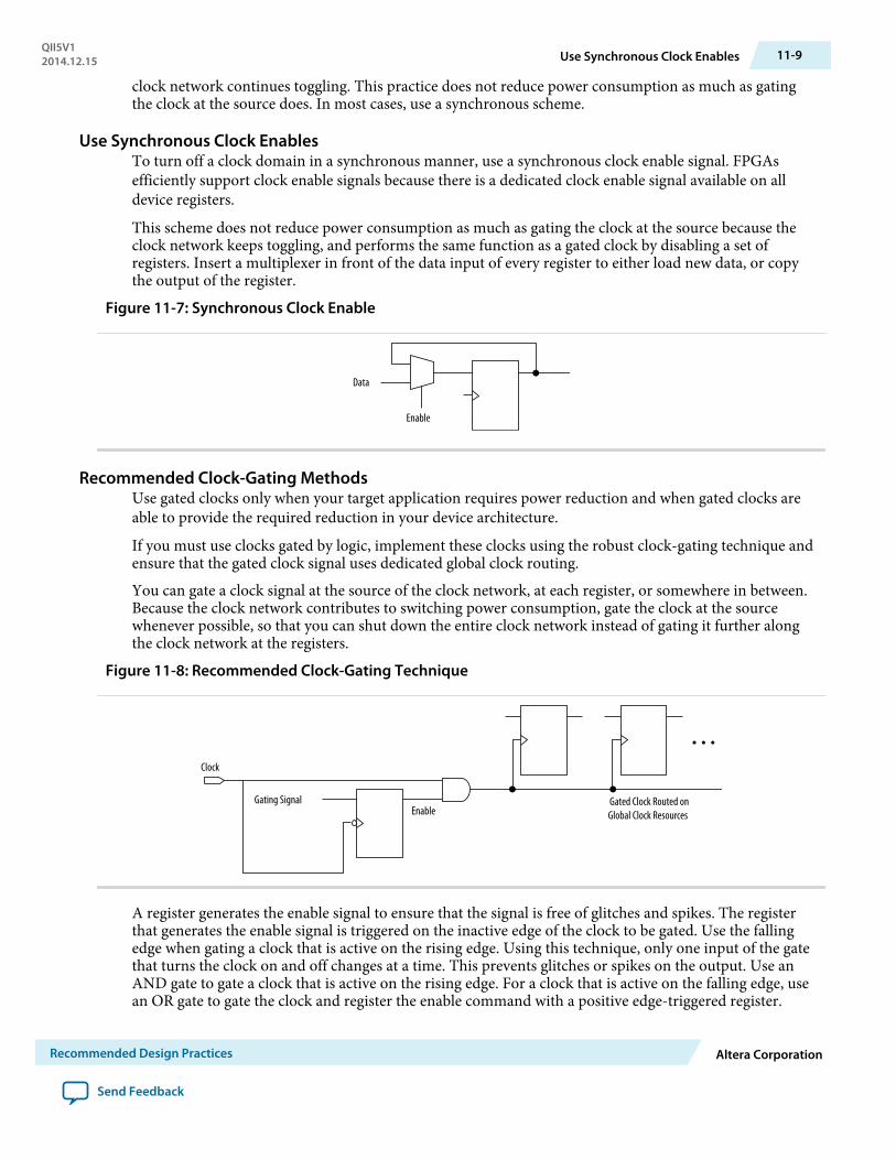
clock network continues toggling. This practice does not reduce power consumption as much as gatingthe clock at the source does. In most cases, use a synchronous scheme.
Use Synchronous Clock EnablesTo turn off a clock domain in a synchronous manner, use a synchronous clock enable signal. FPGAsefficiently support clock enable signals because there is a dedicated clock enable signal available on alldevice registers.
This scheme does not reduce power consumption as much as gating the clock at the source because theclock network keeps toggling, and performs the same function as a gated clock by disabling a set ofregisters. Insert a multiplexer in front of the data input of every register to either load new data, or copythe output of the register.
Figure 11-7: Synchronous Clock Enable
Enable
Data
Recommended Clock-Gating MethodsUse gated clocks only when your target application requires power reduction and when gated clocks areable to provide the required reduction in your device architecture.
If you must use clocks gated by logic, implement these clocks using the robust clock-gating technique andensure that the gated clock signal uses dedicated global clock routing.
You can gate a clock signal at the source of the clock network, at each register, or somewhere in between.Because the clock network contributes to switching power consumption, gate the clock at the sourcewhenever possible, so that you can shut down the entire clock network instead of gating it further alongthe clock network at the registers.
Figure 11-8: Recommended Clock-Gating Technique
Clock
EnableGated Clock Routed on Global Clock Resources
Gating Signal
A register generates the enable signal to ensure that the signal is free of glitches and spikes. The registerthat generates the enable signal is triggered on the inactive edge of the clock to be gated. Use the fallingedge when gating a clock that is active on the rising edge. Using this technique, only one input of the gatethat turns the clock on and off changes at a time. This prevents glitches or spikes on the output. Use anAND gate to gate a clock that is active on the rising edge. For a clock that is active on the falling edge, usean OR gate to gate the clock and register the enable command with a positive edge-triggered register.
QII5V12014.12.15 Use Synchronous Clock Enables 11-9
Recommended Design Practices Altera Corporation
Send Feedback

When using this technique, pay close attention to the duty cycle of the clock and the delay through thelogic that generates the enable signal because you must generate the enable command in one-half theclock cycle. This situation might cause problems if the logic that generates the enable command is particu‐larly complex, or if the duty cycle of the clock is severely unbalanced. However, careful management ofthe duty cycle and logic delay may be an acceptable solution when compared with problems created byother methods of gating clocks.
Ensure that you apply a clock setting to the gated clock in the TimeQuest analyzer. Apply a clock settingto the output of the AND gate. Otherwise, the timing analyzer might analyze the circuit using the clockpath through the register as the longest clock path and the path that skips the register as the shortest clockpath, resulting in artificial clock skew.
In certain cases, converting the gated clocks to clock enables may help reduce glitch and clock skew, andeventually produce a more accurate timing analysis. You can set the Quartus II software to automaticallyconvert gated clocks to clock enables by turning on the Auto Gated Clock Conversion option. Theconversion applies to two types of gated clocking schemes: single-gated clock and cascaded-gated clock.
Optimizing Physical Implementation and Timing ClosureThis section provides design and timing closure techniques for high speed or complex core logic designswith challenging timing requirements. These techniques may also be helpful for low or medium speeddesigns.
Planning Physical ImplementationWhen planning a design, consider the following elements of physical implementation:
• The number of unique clock domains and their relationships• The amount of logic in each functional block• The location and direction of data flow between blocks• How data routes to the functional blocks between I/O interfaces
Interface-wide control or status signals may have competing or opposing constraints. For example,when a functional block's control or status signals interface with physical channels from both sides ofthe device. In such cases you must provide enough pipeline register stages to allow these signals totraverse the width of the device. In addition, you can structure the hierarchy of the design into separatelogic modules for each side of the device. The side modules can generate and use registered controlsignals per side. This simplifies floorplanning, particularly in designs with transceivers, by placing per-side logic near the transceivers.
When adding register stages to pipeline control signals, turn off the Auto Shift Register Replacementoption (Assignments > Settings > Compiler Settings > Advanced Settings (Synthesis)) for theseregisters. By default, chains of registers can be converted to a RAM-based implementation based onperformance and resource estimates. Since pipelining helps meet timing requirements over longdistance, this assignment ensures that control signals are not converted.
Planning FPGA ResourcesYour design requirements impact the use of FPGA resources. Plan functional blocks with appropriateglobal, regional, and dual-regional network signals in mind.
In general, after allocating the clocks in a design, use global networks for the highest fan-out controlsignals. When a global network signal distributes a high fan-out control signal, the global signal can drivelogic anywhere in the device. Similarly, when using a regional network signal, the driven must be in onequadrant of the device, or half the device for a dual-regional network signal. Depending on data flow andphysical locations of the data entry and exit between the I/Os and the device, restricting a functional blockto a quadrant or half the device may not be practical for performance or resource requirements.
11-10 Optimizing Physical Implementation and Timing ClosureQII5V1
2014.12.15
Altera Corporation Recommended Design Practices
Send Feedback

When floorplanning a design, consider the balance of different types of device resources, such as memory,logic, and DSP blocks in the main functional blocks. For example, if a design is memory intensive with asmall amount of logic, it may be difficult to develop an effective floorplan. Logic that interfaces with thememory would have to spread across the chip to access the memory. In this case, it is important to useenough register stages in the data and control paths to allow signals to traverse the chip to access thephysically disparate resources needed.
Optimizing Timing ClosureYou can make changes to your design and constraints that help you achieve timing closure.
Whenever you change the project settings, you must balance any performance improvement of the settingagainst any potential increase in compilation time associated with the setting. You can view the perform‐ance gain versus runtime cost by reviewing the Fitter messages after design processing.
You can use physical synthesis optimizations for combinational logic, register retiming, and registerduplication techniques to optimize your design for timing closure.
Click Assignments > Settings > Compiler Settings > Advanced Settings (Fitter) to turn on physicalsynthesis options.
• Physical synthesis for combinational logic—When the Perform physical synthesis for combinationallogic is turned on, the report panel identifies logic that physical synthesis can modify. You can use thisinformation to modify the design so that the associated optimization can be turned off to save compiletime.
• Register duplication—This technique is most useful where registers have high fan-out, or where thefan-out is in physically distant areas of the device. Review the netlist optimizations report and considermanually duplicating registers automatically added by physical synthesis. You can also locate theoriginal and duplicate registers in the Chip Planner. Compare their locations, and if the fan-out isimproved, modify the code and turn off register duplication to save compile time.
• Register retiming—This technique is particularly useful where some combinatorial paths betweenregisters exceed the timing goal while other paths fall short. If a design is already heavily pipelined,register retiming is less likely to provide significant performance gains since there should not besignificantly unbalanced levels of logic across pipeline stages.
The application of appropriate timing constraints is essential to timing closure. Use the followinggeneral guidelines in applying timing constraints:
• Apply multicycle constraints in your design wherever single-cycle timing analysis is not required.• Apply False Path constraints to all asynchronous clock domain crossings or resets in the design. This
technique prevents overconstraining and the Fitter focuses only on critical paths to reduce compiletime. However, over constraining timing critical clock domains can sometimes provide better timingresults and lower compile times than physical synthesis.
• Overconstrain rather than using physical synthesis when the slack improvement from physicalsynthesis is near zero. Overconstrain the frequency requirement on timing critical clock domains byusing setup uncertainty.
• When evaluating the effect of constraint changes on performance and runtime, compile the designwith at least three different seeds to determine the average performance and runtime effects. Differentconstraint combinations produce various results. Three samples or more establishes a performancetrend. Modify your constraints based on performance improvement or decline.
• Leave settings at the default value whenever possible. Increasing performance constraints can increasethe compile time significantly. While those increases may be necessary to close timing on a design,using the default settings whenever possible minimizes compile time.
QII5V12014.12.15 Optimizing Timing Closure 11-11
Recommended Design Practices Altera Corporation
Send Feedback

Optimizing Critical Timing PathsTo close timing in high speed designs, review paths with the largest timing failures. Correcting a single,large timing failure can result in a very significant timing improvement.
Review the register placement and routing paths by clicking Tools > Chip Planner. Large timing failureson high fan-out control signals can be caused by any of the following conditions:
• Sub-optimal use of global networks• Signals that traverse the chip on local routing without pipelining• Failure to correct high fan-out by register duplication
For high-speed and high-bandwidth designs, optimize speed by reducing bus width and wire usage. Toreduce wire use, move the data as little as possible. For example, if a block of logic functions on a fewbits of a word, store inactive bits in a fifo or memory. Memory is cheaper and denser than registers andreduces wire usage.
Optimizing Power ConsumptionThe total FPGA power consumption is comprised of I/O power, core static power, and core dynamicpower. Knowledge of the relationship between these components is fundamental in calculating the overalltotal power consumption.
You can use various optimization techniques and tools to minimize power consumption when appliedduring FPGA design implementation. The Quartus II software offers power-driven compilation featuresto fully optimize device power consumption. Power-driven compilation focuses on reducing your design’stotal power consumption using power-driven synthesis and power-driven placement and routing.
Managing Design MetastabilityMetastability in PLD designs can be caused by the synchronization of asynchronous signals. You can usethe Quartus II software to analyze the mean time between failures (MTBF) due to metastability, thusoptimizing the design to improve the metastability MTBF. A high metastability MTBF indicates a morerobust design.
Related InformationViewing Metastability ReportsFor more information about viewing metastability reports, refer to Viewing Metastability Reports inQuartus II Help.
Checking Design ViolationsTo improve the reliability, timing performance, and logic utilization of your design, avoid design ruleviolations. The Quartus II software provides the Design Assistant tool that automatically checks for designrule violations and reports their location.
The Design Assistant is a design rule checking tool that allows you to check for design issues early in thedesign flow. The Design Assistant checks your design for adherence to Altera-recommended designguidelines. You can specify which rules you want the Design Assistant to apply to your design. This isuseful if you know that your design violates particular rules that are not critical and you can allow theserule violations. The Design Assistant generates design violation reports with details about each violationbased on the settings that you specified.
11-12 Optimizing Critical Timing PathsQII5V1
2014.12.15
Altera Corporation Recommended Design Practices
Send Feedback

This section provides an introduction to the Quartus II design flow with the Design Assistant, messageseverity levels, and an explanation about how to set up the Design Assistant. The last parts of the sectiondescribe the design rules and the reports generated by the Design Assistant. The Design Assistantsupports all Altera devices supported by the Quartus II software.
Validating Against Design RulesYou can run the Design Assistant following design synthesis or compilation. The Design Assistantperforms a post-fit netlist analysis of your design.
The default is to apply all of the rules to your project. If there are some rules that are unimportant to yourdesign, you can turn off the rules that you do not want the Design Assistant to use.
Figure 11-9: Quartus II Design Flow with the Design Assistant
Design Files
Analysis & Elaboration
Synthesis(Logic Synthesis &
Technology Mapping)
Fitter
T iming Analysis
Design Assistant
Pre-SynthesisNetlist
Design AssistantGolden Rules (1)
Rule V iolationReport
CustomRules (2)
Post-FittingNetlist
Post-SynthesisNetlist
1. Database of the default rules for the Design Assistant.2. A file that contains the .xml codes of the custom rules for the Design Assistant. For more details about
how to create this file .
The Design Assistant analyzes your design netlist at different stages of the compilation flow and mayyield different warnings or errors, even though the netlists are functionally the same. Your pre-synthesis, post-synthesis, and post-fitting netlists might be different due to optimizations performedby the Quartus II software. For example, a warning message in a pre-synthesis netlist may be removedafter the netlist has been synthesized into a post-synthesis or post-fitting netlist.
The exact operation of the Design Assistant depends on when you run it:
QII5V12014.12.15 Validating Against Design Rules 11-13
Recommended Design Practices Altera Corporation
Send Feedback

• When you run the Design Assistant after running a full compilation or fitting, the Design Assistantperforms a post-fitting analysis on the design.
• When you run the Design Assistant after performing Analysis and Synthesis, the Design Assistantperforms post-synthesis analysis on the design.
• When you start the Design Assistant after performing Analysis and Elaboration, the Design Assistantperforms a pre-synthesis analysis on the design. You can also perform pre-synthesis analysis with theDesign Assistant using the command-line. You can use the -rtl option with the quartus_drcexecutable, as shown in the following example:
quartus_drc <project_name> --rtl=on
If your design violates a design rule, the Design Assistant generates warning messages and informationmessages about the violated rule. The Design Assistant displays these messages in the Messageswindow, in the Design Assistant Messages report, and in the Design Assistant report files. You can findthe Design Assistant report files called <project_name>.drc.rpt in the <project_name> subdirectory ofthe project directory.
Related InformationAbout the Design Assistant
Creating Custom Design RulesYou can define and validate your design against your own custom set of design rules. You can save theserules in a text file (with any file extension) with the XML format.
You then specify the path to that file in the Design Assistant settings page and run the Design Assistantfor violation checking.
Refer to the following location to locate the file that contains the default rules for the Design Assistant:
<Quartus II install path>\quartus\libraries\design-assistant\da_golden_rule.xml
Custom Design Rule ExamplesThe following examples of custom rules show how to check node relationships and clock relationships ina design.
This example shows the XML codes for checking SR latch structures in a design.
Example 11-1: Detecting SR Latches in a Design
<DA_RULE ID="EX01" SEVERITY="CRITICAL" NAME="Checking Design for SR Latch" DEFAULT_RUN="YES"><RULE_DEFINITION> <FORBID> <OR> <NODE NAME="NODE_1" TYPE="SRLATCH" /> <HAS_NODE NODE_LIST="NODE_1" /> <NODE NAME="NODE_1" TOTAL_FANIN="EQ2" /> <NODE NAME="NODE_2" TOTAL_FANIN="EQ2" /> <AND> <NODE_RELATIONSHIP FROM_NAME="NODE_1" FROM_TYPE="NAND" TO_NAME="NODE_2" TO_TYPE="NAND" /> <NODE_RELATIONSHIP FROM_NAME="NODE_2" FROM_TYPE="NAND" TO_NAME="NODE_1" TO_TYPE="NAND" /> </AND> <AND> <NODE_RELATIONSHIP FROM_NAME="NODE_1" FROM_TYPE="NOR" TO_NAME="NODE_2" TO_TYPE="NOR" />
11-14 Creating Custom Design RulesQII5V1
2014.12.15
Altera Corporation Recommended Design Practices
Send Feedback

<NODE_RELATIONSHIP FROM_NAME="NODE_2" FROM_TYPE="NOR" TO_NAME="NODE_1" TO_TYPE="NOR" /> </AND> </OR> </FORBID></RULE_DEFINITION>
<REPORTING_ROOT> <MESSAGE NAME="Rule %ARG1%: Found %ARG2% node(s) related to this rule."> <MESSAGE_ARGUMENT NAME="ARG1" TYPE="ATTRIBUTE" VALUE="ID" /> <MESSAGE_ARGUMENT NAME="ARG2" TYPE="TOTAL_NODE" VALUE="NODE_1" /> </MESSAGE></REPORTING_ROOT></DA_RULE>
The possible SR latch structures are specified in the rule definition section. Codes defined in the<AND></AND> block are tied together, meaning that each statement in the block must be true forthe block to be fulfilled (AND gate similarity). In the <OR></OR> block, as long as one statementin the block is true, the block is fulfilled (OR gate similarity). If no <AND></AND> or <OR></OR>blocks are specified, the default is <AND></AND>.
The <FORBID></FORBID> section contains the undesirable condition for the design, which in thiscase is the SR latch structures. If the condition is fulfilled, the Design Assistant highlights a ruleviolation.
Example 11-2: Detecting SR Latches in a Design
<AND> <NODE_RELATIONSHIP FROM_NAME="NODE_1" FROM_TYPE="NAND" TO_NAME="NODE_2" TO_TYPE="NAND" /> <NODE_RELATIONSHIP FROM_NAME="NODE_2" FROM_TYPE="NAND" TO_NAME="NODE_1" TO_TYPE="NAND" /></AND>
Figure 11-10: Undesired Condition 1
NAND2
NODE_1
NAND2
NODE_2
<AND> <NODE_RELATIONSHIP FROM_NAME="NODE_1" FROM_TYPE="NOR" TO_NAME="NODE_2" TO_TYPE="NOR" /> <NODE_RELATIONSHIP FROM_NAME="NODE_2" FROM_TYPE="NOR" TO_NAME="NODE_1" TO_TYPE="NOR" /></AND>
QII5V12014.12.15 Custom Design Rule Examples 11-15
Recommended Design Practices Altera Corporation
Send Feedback

Figure 11-11: Undesired Condition 2
This example shows how to use the CLOCK_RELATIONSHIP attribute to relate nodes to clockdomains. This example checks for correct synchronization in data transfer between asynchronousclock domains. Synchronization is done with cascaded registers, also called synchronizers, at thereceiving clock domain. The code in This example checks for the synchronizer configurationbased on the following guidelines:
• The cascading registers need to be triggered on the same clock edge• There is no logic between the register output of the transmitting clock domain and the
cascaded registers in the receiving asynchronous clock domain.
Example 11-3: Detecting Incorrect Synchronizer Configuration
<DA_RULE ID="EX02" SEVERITY="HIGH" NAME="Data Transfer Not Synch Correctly" DEFAULT_RUN="YES">
<RULE_DEFINITION><DECLARE> <NODE NAME="NODE_1" TYPE="REG" /> <NODE NAME="NODE_2" TYPE="REG" /> <NODE NAME="NODE_3" TYPE="REG" /> </DECLARE><FORBID> <NODE_RELATIONSHIP FROM_NAME="NODE_1" TO_NAME="NODE_2" TO_PORT="D_PORT" CLOCK_RELATIONSHIP="ASYN" /> <NODE_RELATIONSHIP FROM_NAME="NODE_2" TO_NAME="NODE_3" TO_PORT="D_PORT" CLOCK_RELATIONSHIP="!ASYN" /> <OR> <NODE_RELATIONSHIP FROM_NAME="NODE_1" TO_NAME="NODE_2" TO_PORT="D_PORT" REQUIRED_THROUGH="YES" THROUGH_TYPE="COMB" CLOCK_RELATION-SHIP="ASYN" /> <CLOCK_RELATIONSHIP NAME="SEQ_EDGE|ASYN" NODE_LIST="NODE_2, NODE_3" /> </OR></FORBID></RULE_DEFINITION>
<REPORTING_ROOT><MESSAGE NAME="Rule %ARG1%: Found %ARG2% node(s) related to this rule."> <MESSAGE_ARGUMENT NAME="ARG1" TYPE="ATTRIBUTE" VALUE="ID" /> <MESSAGE_ARGUMENT NAME="ARG2" TYPE="TOTAL_NODE" VALUE="NODE_1" /> <MESSAGE NAME="Source node(s): %ARG3%, Destination node(s): %ARG4%"> <MESSAGE_ARGUMENT NAME="ARG3" TYPE="NODE" VALUE="NODE_1" /> <MESSAGE_ARGUMENT NAME="ARG4" TYPE="NODE" VALUE="NODE_2" /> </MESSAGE>
11-16 Custom Design Rule ExamplesQII5V1
2014.12.15
Altera Corporation Recommended Design Practices
Send Feedback

</MESSAGE></REPORTING_ROOT></DA_RULE>
The codes differentiate the clock domains. ASYN means asynchronous, and !ASYN means non-asynchronous. This notation is useful for describing nodes that are in different clock domains.The following lines from the example state that NODE_2 and NODE_3 are in the same clock domain,but NODE_1 is not.
<NODE_RELATIONSHIP FROM_NAME="NODE_1" TO_NAME="NODE_2" TO_PORT="D_PORT" CLOCK_RELATIONSHIP="ASYN" />
<NODE_RELATIONSHIP FROM_NAME="NODE_2" TO_NAME="NODE_3" TO_PORT="D_PORT" CLOCK_RELATIONSHIP="!ASYN" />
The next line of code states that NODE_2 and NODE_3 have a clock relationship of either sequentialedge or asynchronous.
<CLOCK_RELATIONSHIP NAME="SEQ_EDGE|ASYN" NODE_LIST="NODE_2, NODE_3" />
The <FORBID></FORBID> section contains the undesirable condition for the design, which in thiscase is the undesired configuration of the synchronizer. If the condition is fulfilled, the DesignAssistant highlights a rule violation.
The possible SR latch structures are specified in the rule definition section. Codes defined in the<AND></AND> block are tied together, meaning that each statement in the block must be true forthe block to be fulfilled (AND gate similarity). In the <OR></OR> block, as long as one statementin the block is true, the block is fulfilled (OR gate similarity). If no <AND></AND> or <OR></OR>blocks are specified, the default is <AND></AND>.
The <FORBID></FORBID> section contains the undesirable condition for the design, which in thiscase is the SR latch structures. If the condition is fulfilled, the Design Assistant highlights a ruleviolation.
The following examples show the undesired conditions from with their equivalent blockdiagrams:
Example 11-4: Undesired Condition 3
<NODE_RELATIONSHIP FROM_NAME="NODE_1" TO_NAME="NODE_2" TO_PORT="D_PORT" CLOCK_RELATIONSHIP="ASYN" />
<NODE_RELATIONSHIP FROM_NAME="NODE_2" TO_NAME="NODE_3" TO_PORT="D_PORT" CLOCK_RELATIONSHIP="!ASYN" />
<NODE_RELATIONSHIP FROM_NAME="NODE_1" TO_NAME="NODE_2" TO_PORT="D_PORT" REQUIRED_THROUGH="YES" THROUGH_TYPE="COMB" CLOCK_RELATIONSHIP="ASYN" />
QII5V12014.12.15 Custom Design Rule Examples 11-17
Recommended Design Practices Altera Corporation
Send Feedback

Figure 11-12: Undesired Condition 3
NODE_1
Logic
NODE_2 NODE_3
D
CLOCK_1
CLOCK_2
Q
Example 11-5: Undesired Condition 4
<NODE_RELATIONSHIP FROM_NAME="NODE_1" TO_NAME="NODE_2" TO_PORT="D_PORT" CLOCK_RELATIONSHIP="ASYN" />
<NODE_RELATIONSHIP FROM_NAME="NODE_2" TO_NAME="NODE_3" TO_PORT="D_PORT" CLOCK_RELATIONSHIP="!ASYN" />
<CLOCK_RELATIONSHIP NAME="SEQ_EDGE|ASYN" NODE_LIST="NODE_2, NODE_3" />
Figure 11-13: Undesired Condition 4
NODE_1 NODE_2 NODE_3
D
CLOCK_1
CLOCK_2
Q
Use Clock and Register-Control Architectural FeaturesIn addition to following general design guidelines, you must code your design with the device architecturein mind. FPGAs provide device-wide clocks and register control signals that can improve performance.
Use Global Clock Network ResourcesAltera FPGAs provide device-wide global clock routing resources and dedicated inputs. Use the FPGA’slow-skew, high fan-out dedicated routing where available.
By assigning a clock input to one of these dedicated clock pins or with a Quartus II logic option to assignglobal routing, you can take advantage of the dedicated routing available for clock signals.
In an ASIC design, you should balance the clock delay as it is distributed across the device. Because AlteraFPGAs provide device-wide global clock routing resources and dedicated inputs, there is no need tomanually balance delays on the clock network.
11-18 Use Clock and Register-Control Architectural FeaturesQII5V1
2014.12.15
Altera Corporation Recommended Design Practices
Send Feedback

You should limit the number of clocks in your design to the number of dedicated global clock resourcesavailable in your FPGA. Clocks feeding multiple locations that do not use global routing may exhibit clockskew across the device that could lead to timing problems. In addition, when you use combinational logicto generate an internal clock, it adds delays on the clock path. In some cases, delay on a clock line canresult in a clock skew greater than the data path length between two registers. If the clock skew is greaterthan the data delay, you violate the timing parameters of the register (such as hold time requirements) andthe design does not function correctly.
FPGAs offer a number of low-skew global routing resources to distribute high fan-out signals to help withthe implementation of large designs with many clock domains. Many large FPGA devices providededicated global clock networks, regional clock networks, and dedicated fast regional clock networks.These clocks are organized into a hierarchical clock structure that allows many clocks in each deviceregion with low skew and delay. There are typically several dedicated clock pins to drive either global orregional clock networks, and both PLL outputs and internal clocks can drive various clock networks.
To reduce clock skew in a given clock domain and ensure that hold times are met in that clock domain,assign each clock signal to one of the global high fan-out, low-skew clock networks in the FPGA device.The Quartus II software automatically uses global routing for high fan-out control signals, PLL outputs,and signals feeding the global clock pins on the device. You can make explicit Global Signal logic optionsettings by turning on the Global Signal option setting. Use this option when it is necessary to force thesoftware to use the global routing for particular signals.
To take full advantage of these routing resources, the sources of clock signals in a design (input clock pinsor internally-generated clocks) need to drive only the clock input ports of registers. In older Altera devicefamilies, if a clock signal feeds the data ports of a register, the signal may not be able to use dedicatedrouting, which can lead to decreased performance and clock skew problems. In general, allowing clocksignals to drive the data ports of registers is not considered synchronous design and can complicatetiming analysis.
Use Global Reset ResourcesASIC designs may use local resets to avoid long routing delays. Take advantage of the device-wideasynchronous reset pin available on most FPGAs to eliminate these problems. This reset signal provideslow-skew routing across the device.
The following are three types of resets used in synchronous circuits:
• Synchronous Reset• Asynchronous Reset• Synchronized Asynchronous Reset—preferred when designing an FPGA circuit
Use Synchronous ResetsThe synchronous reset ensures that the circuit is fully synchronous. You can easily time the circuit withthe Quartus II TimeQuest analyzer.
Because clocks that are synchronous to each other launch and latch the reset signal, the data arrival anddata required times are easily determined for proper slack analysis. The synchronous reset is easier to usewith cycle-based simulators.
There are two methods by which a reset signal can reach a register; either by being gated in with the datainput, or by using an LAB-wide control signal (synclr). If you use the first method, you risk adding anadditional gate delay to the circuit to accommodate the reset signal, which causes increased data arrivaltimes and negatively impacts setup slack. The second method relies on dedicated routing in the LAB toeach register, but this is slower than an asynchronous reset to the same register.
QII5V12014.12.15 Use Global Reset Resources 11-19
Recommended Design Practices Altera Corporation
Send Feedback

Figure 11-14: Synchronous Reset
DFFAND2
inst1
Figure 11-15: LAB-Wide Control Signals
Dedicated Row LAB Clocks
Local Interconnect
Local Interconnect
Local Interconnect
Local Interconnect
Local Interconnect
Local Interconnect
There are two uniqueclock signals per LAB
6
6
6
labclk0
labclkena0
labclk1 labclk2 syncload labclr1
labclkena1 labclkena2 labclr0 synclr
Consider two types of synchronous resets when you examine the timing analysis of synchronous resets—externally synchronized resets and internally synchronized resets. Externally synchronized resets aresynchronized to the clock domain outside the FPGA, and are not very common. A power-on asynchro‐nous reset is dual-rank synchronized externally to the system clock and then brought into the FPGA.Inside the FPGA, gate this reset with the data input to the registers to implement a synchronous reset.
11-20 Use Synchronous ResetsQII5V1
2014.12.15
Altera Corporation Recommended Design Practices
Send Feedback

Figure 11-16: Externally Synchronized Reset
por_n
clockreset_n
data_a
INPU TVCC
VCCINPU T
VCCINPU Tclock
VCCINPU Tdata_b
AND2
lc 1
AND2
lc 2
OUTPU T out_a
out_bOUTPU T
FPG A
The following example shows the Verilog equivalent of the schematic. When you use synchronous resets,the reset signal is not put in the sensitivity list.
The following example shows the necessary modifications that you should make to the internallysynchronized reset.
Example 11-6: Verilog Code for Externally Synchronized Reset
module sync_reset_ext ( input clock, input reset_n, input data_a, input data_b, output out_a, output out_b );reg reg1, reg2assign out_a = reg1;assign out_b = reg2;always @ (posedge clock)begin if (!reset_n) begin reg1 <= 1’b0; reg2 <= 1’b0; end else begin reg1 <= data_a; reg2 <= data_b; endendendmodule // sync_reset_ext
The following example shows the constraints for the externally synchronous reset. Because theexternal reset is synchronous, you only need to constrain the reset_n signal as a normal inputsignal with set_input_delay constraint for -max and -min.
QII5V12014.12.15 Use Synchronous Resets 11-21
Recommended Design Practices Altera Corporation
Send Feedback

Example 11-7: SDC Constraints for Externally Synchronized Reset
# Input clock - 100 MHzcreate_clock [get_ports {clock}] \ -name {clock} \ -period 10.0 \ -waveform {0.0 5.0}# Input constraints on low-active reset# and dataset_input_delay 7.0 \ -max \ -clock [get_clocks {clock}] \ [get_ports {reset_n data_a data_b}]set_input_delay 1.0 \ -min \ -clock [get_clocks {clock}] \ [get_ports {reset_n data_a data_b}]
More often, resets coming into the device are asynchronous, and must be synchronized internallybefore being sent to the registers.
Figure 11-17: Internally Synchronized Reset
INPU TVCC
VCCINPU T
VCCINPU T
VCCINPU T
AND2
lc 1
AND2
lc 2
OUTPU T
OUTPU T
The following example shows the Verilog equivalent of the schematic. Only the clock edge is inthe sensitivity list for a synchronous reset.
Example 11-8: Verilog Code for Internally Synchronized Reset
module sync_reset_ext ( input clock, input reset_n, input data_a, input data_b, output out_a, output out_b );reg reg1, reg2assign out_a = reg1;
11-22 Use Synchronous ResetsQII5V1
2014.12.15
Altera Corporation Recommended Design Practices
Send Feedback

assign out_b = reg2;always @ (posedge clock)begin if (!reset_n) begin reg1 <= 1’b0; reg2 <= 1’b0; end else begin reg1 <= data_a; reg2 <= data_b; endendendmodule // sync_reset_ext
The SDC constraints are similar to the external synchronous reset, except that the input resetcannot be constrained because it is asynchronous and should be cut with a set_false_pathstatement to avoid these being considered as unconstrained paths.
Example 11-9: SDC Constraints for Internally Synchronized Reset
# Input clock - 100 MHzcreate_clock [get_ports {clock}] \ -name {clock} \ -period 10.0 \ -waveform {0.0 5.0}# Input constraints on dataset_input_delay 7.0 \ -max \ -clock [get_clocks {clock}] \ [get_ports {data_a data_b}]set_input_delay 1.0 \ -min \ -clock [get_clocks {clock}] \ [get_ports {data_a data_b}]# Cut the asynchronous reset inputset_false_path \ -from [get_ports {reset_n}] \ -to [all_registers]
An issue with synchronous resets is their behavior with respect to short pulses (less than a period)on the asynchronous input to the synchronizer flipflops. This can be a disadvantage because theasynchronous reset requires a pulse width of at least one period wide to guarantee that it iscaptured by the first flipflop. However, this can also be viewed as an advantage in that this circuitincreases noise immunity. Spurious pulses on the asynchronous input have a lower chance ofbeing captured by the first flipflop, so the pulses do not trigger a synchronous reset. In somecases, you might want to increase the noise immunity further and reject any asynchronous inputreset that is less than n periods wide to debounce an asynchronous input reset.
QII5V12014.12.15 Use Synchronous Resets 11-23
Recommended Design Practices Altera Corporation
Send Feedback

Figure 11-18: Internally Synchronized Reset with Pulse Extender
INPU TVCC
VCCINPU T
VCCINPU T
VCCINPU T
AND2
lc 1
AND2
lc 2
OUTPU T
OUTPU T
BNAND2
Synchronizer Flip-Flops n Pulse Extender Flip-Flops
lc 3
1. Junction dots indicate the number of stages. You can have more flip flops to get a wider pulsethat spans more clock cycles.
Many designs have more than one clock signal. In these cases, use a separate reset synchroni‐zation circuit for each clock domain in the design. When you create synchronizers for PLLoutput clocks, these clock domains are not reset until you lock the PLL and the PLL outputclocks are stable. If you use the reset to the PLL, this reset does not have to be synchronouswith the input clock of the PLL. You can use an asynchronous reset for this. Using a reset tothe PLL further delays the assertion of a synchronous reset to the PLL output clock domainswhen using internally synchronized resets.
Using Asynchronous ResetsAsynchronous resets are the most common form of reset in circuit designs, as well as the easiest toimplement. Typically, you can insert the asynchronous reset into the device, turn on the global buffer, andconnect to the asynchronous reset pin of every register in the device.
This method is only advantageous under certain circumstances—you do not need to always reset theregister. Unlike the synchronous reset, the asynchronous reset is not inserted in the data path, and doesnot negatively impact the data arrival times between registers. Reset takes effect immediately, and as soonas the registers receive the reset pulse, the registers are reset. The asynchronous reset is not dependent onthe clock.
However, when the reset is deasserted and does not pass the recovery (µtSU) or removal (µtH) time check(the TimeQuest analyzer recovery and removal analysis checks both times), the edge is said to have falleninto the metastability zone. Additional time is required to determine the correct state, and the delay cancause the setup time to fail to register downstream, leading to system failure. To avoid this, add a fewfollower registers after the register with the asynchronous reset and use the output of these registers in thedesign. Use the follower registers to synchronize the data to the clock to remove the metastability issues.You should place these registers close to each other in the device to keep the routing delays to a minimum,which decreases data arrival times and increases MTBF. Ensure that these follower registers themselvesare not reset, but are initialized over a period of several clock cycles by “flushing out” their current orinitial state.
11-24 Using Asynchronous ResetsQII5V1
2014.12.15
Altera Corporation Recommended Design Practices
Send Feedback

Figure 11-19: Asynchronous Reset with Follower Registers
DFF DFF DFF
INPU TVCC
VCCINPU T
VCCINPU T
out_aOUTPU T
The following example shows the equivalent Verilog code. The active edge of the reset is now in thesensitivity list for the procedural block, which infers a clock enable on the follower registers with theinverse of the reset signal tied to the clock enable. The follower registers should be in a separateprocedural block as shown using non-blocking assignments.
Example 11-10: Verilog Code of Asynchronous Reset with Follower Registers
module async_reset ( input clock, input reset_n, input data_a, output out_a, );reg reg1, reg2, reg3;assign out_a = reg3;always @ (posedge clock, negedge reset_n)begin if (!reset_n) reg1 <= 1’b0; else reg1 <= data_a;endalways @ (posedge clock)begin reg2 <= reg1; reg3 <= reg2;endendmodule // async_reset
You can easily constrain an asynchronous reset. By definition, asynchronous resets have a non-deterministic relationship to the clock domains of the registers they are resetting. Therefore, statictiming analysis of these resets is not possible and you can use the set_false_path command toexclude the path from timing analysis. Because the relationship of the reset to the clock at theregister is not known, you cannot run recovery and removal analysis in the TimeQuest analyzerfor this path. Attempting to do so even without the false path statement results in no pathsreported for recovery and removal.
Example 11-11: SDC Constraints for Asynchronous Reset
# Input clock - 100 MHzcreate_clock [get_ports {clock}] \
QII5V12014.12.15 Using Asynchronous Resets 11-25
Recommended Design Practices Altera Corporation
Send Feedback

-name {clock} \ -period 10.0 \ -waveform {0.0 5.0}# Input constraints on dataset_input_delay 7.0 \ -max \ -clock [get_clocks {clock}]\ [get_ports {data_a}]set_input_delay 1.0 \ -min \ -clock [get_clocks {clock}] \ [get_ports {data_a}]# Cut the asynchronous reset inputset_false_path \ -from [get_ports {reset_n}] \ -to [all_registers]
The asynchronous reset is susceptible to noise, and a noisy asynchronous reset can cause aspurious reset. You must ensure that the asynchronous reset is debounced and filtered. You caneasily enter into a reset asynchronously, but releasing a reset asynchronously can lead to potentialproblems (also referred to as “reset removal”) with metastability, including the hazards ofunwanted situations with synchronous circuits involving feedback.
Use Synchronized Asynchronous ResetTo avoid potential problems associated with purely synchronous resets and purely asynchronous resets,you can use synchronized asynchronous resets. Synchronized asynchronous resets combine theadvantages of synchronous and asynchronous resets.
These resets are asynchronously asserted and synchronously deasserted. This takes effect almost instanta‐neously, and ensures that no data path for speed is involved, and that the circuit is synchronous for timinganalysis and is resistant to noise.
The following example shows a method for implementing the synchronized asynchronous reset. Youshould use synchronizer registers in a similar manner as synchronous resets. However, the asynchronousreset input is gated directly to the CLRN pin of the synchronizer registers and immediately asserts theresulting reset. When the reset is deasserted, logic “1” is clocked through the synchronizers to synchro‐nously deassert the resulting reset.
11-26 Use Synchronized Asynchronous ResetQII5V1
2014.12.15
Altera Corporation Recommended Design Practices
Send Feedback

Figure 11-20: Schematic of Synchronized Asynchronous Reset
DFF
reg3
VCC
DFF
reg4
DFF
reg1
DFF
reg2
data_a
clock
INPU TVCC
VCCINPU T
VCCINPU Treset_n
VCCINPU Tdata_b
out_aOUTPU T
out_bOUTPU T
The following example shows the equivalent Verilog HDL code. Use the active edge of the reset in thesensitivity list for the blocks.
Example 11-12: Verilog Code for Synchronized Asynchronous Reset
module sync_async_reset ( input clock, input reset_n, input data_a, input data_b, output out_a, output out_b );reg reg1, reg2;reg reg3, reg4;assign out_a = reg1;assign out_b = reg2;assign rst_n = reg4;always @ (posedge clock, negedge reset_n)begin if (!reset_n) begin reg3 <= 1’b0; reg4 <= 1’b0; end else begin reg3 <= 1’b1; reg4 <= reg3; endendalways @ (posedge clock, negedge rst_n)begin if (!rst_n)
QII5V12014.12.15 Use Synchronized Asynchronous Reset 11-27
Recommended Design Practices Altera Corporation
Send Feedback

begin reg1 <= 1’b0; reg2 <= 1;b0; end else begin reg1 <= data_a; reg2 <= data_b; endendendmodule // sync_async_reset
To minimize the metastability effect between the two synchronization registers, and to increasethe MTBF, the registers should be located as close as possible in the device to minimize routingdelay. If possible, locate the registers in the same logic array block (LAB). The input reset signal(reset_n) must be excluded with a set_false_path command:
set_false_path -from [get_ports {reset_n}] -to [all_registers]
The set_false_path command used with the specified constraint excludes unnecessary inputtiming reports that would otherwise result from specifying an input delay on the reset pin.
The instantaneous assertion of synchronized asynchronous resets is susceptible to noise and runtpulses. If possible, you should debounce the asynchronous reset and filter the reset before it entersthe device. The circuit ensures that the synchronized asynchronous reset is at least one full clockperiod in length. To extend this time to n clock periods, you must increase the number ofsynchronizer registers to n + 1. You must connect the asynchronous input reset (reset_n) to theCLRN pin of all the synchronizer registers to maintain the asynchronous assertion of the synchron‐ized asynchronous reset.
Avoid Asynchronous Register Control SignalsAvoid using an asynchronous load signal if the design target device architecture does not include registerswith dedicated circuitry for asynchronous loads. Also, avoid using both asynchronous clear and preset ifthe architecture provides only one of these control signals.
Some Altera devices directly support an asynchronous clear function, but not a preset or load function.When the target device does not directly support the signals, the synthesis or placement and routingsoftware must use combinational logic to implement the same functionality. In addition, if you use signalsin a priority other than the inherent priority in the device architecture, combinational logic may berequired to implement the necessary control signals. Combinational logic is less efficient and can causeglitches and other problems; it is best to avoid these implementations.
Implementing Embedded RAMAltera’s dedicated memory architecture offers many advanced features that you can enable with Altera-provided IP cores. Use synchronous memory blocks for your design, so that the blocks can be mappeddirectly into the device dedicated memory blocks.
You can use single-port, dual-port, or three-port RAM with a single- or dual-clocking method. Youshould not infer the asynchronous memory logic as a memory block or place the asynchronous memorylogic in the dedicated memory block, but implement the asynchronous memory logic in regular logiccells.
Altera memory blocks have different read-during-write behaviors, depending on the targeted devicefamily, memory mode, and block type. Read-during-write behavior refers to read and write from the same
11-28 Avoid Asynchronous Register Control SignalsQII5V1
2014.12.15
Altera Corporation Recommended Design Practices
Send Feedback

memory address in the same clock cycle; for example, you read from the same address to which you writein the same clock cycle.
You should check how you specify the memory in your HDL code when you use read-during-writebehavior. The HDL code that describes the read returns either the old data stored at the memory location,or the new data being written to the memory location.
In some cases, when the device architecture cannot implement the memory behavior described in yourHDL code, the memory block is not mapped to the dedicated RAM blocks, or the memory block isimplemented using extra logic in addition to the dedicated RAM block. Implement the read-during-writebehavior using single-port RAM in Arria GX devices and the Cyclone and Stratix series of devices to avoidthis extra logic implementation.
In many synthesis tools, you can specify that the read-during-write behavior is not important to yourdesign; if, for example, you never read and write from the same address in the same clock cycle. ForQuartus II integrated synthesis, add the synthesis attribute ramstyle=”no_rw_check” to allow thesoftware to choose the read-during-write behavior of a RAM, rather than using the read-during-writebehavior specified in your HDL code. Using this type of attribute prevents the synthesis tool from usingextra logic to implement the memory block and, in some cases, can allow memory inference when itwould otherwise be impossible.
Document Revision History
Table 11-1: Document Revision History
Date Version Changes
2014.12.15 14.1.0 Updated location of Fitter Settings, Analysis & Synthesis Settings, and PhysicalOptimization Settings to Compiler Settings.
June 2014 14.0.0 Removed references to obsolete MegaWizard Plug-In Manager.
November2013
13.1.0 Removed HardCopy device information.
May 2013 13.0.0 Removed PrimeTime support.
June 2012 12.0.0 Removed survey link.
November2011
11.0.1 Template update.
May 2011 11.0.0 Added information to Reset Resources .
December2010
10.1.0 • Title changed from Design Recommendations for Altera Devices and theQuartus II Design Assistant.
• Updated to new template.• Added references to Quartus II Help for “Metastability” on page 9–13 and
“Incremental Compilation” on page 9–13.• Removed duplicated content and added references to Quartus II Help for
“Custom Rules” on page 9–15.
QII5V12014.12.15 Document Revision History 11-29
Recommended Design Practices Altera Corporation
Send Feedback

Date Version Changes
July 2010 10.0.0 • Removed duplicated content and added references to Quartus II Help forDesign Assistant settings, Design Assistant rules, Enabling and Disabling DesignAssistant Rules, and Viewing Design Assistant reports.
• Removed information from “Combinational Logic Structures” on page 5–4• Changed heading from “Design Techniques to Save Power” to “Power
Optimization” on page 5–12• Added new “Metastability” section• Added new “Incremental Compilation” section• Added information to “Reset Resources” on page 5–23• Removed “Referenced Documents” section
November2009
9.1.0 • Removed documentation of obsolete rules.
March2009
9.0.0 • No change to content.
November2008
8.1.0 • Changed to 8-1/2 x 11 page size• Added new section “Custom Rules Coding Examples” on page 5–18• Added paragraph to “Recommended Clock-Gating Methods” on page 5–11• Added new section: “Design Techniques to Save Power” on page 5–12
May 2008 8.0.0 • Updated Figure 5–9 on page 5–13; added custom rules file to the flow• Added notes to Figure 5–9 on page 5–13• Added new section: “Custom Rules Report” on page 5–34• Added new section: “Custom Rules” on page 5–34• Added new section: “Targeting Embedded RAM Architectural Features” on
page 5–38• Minor editorial updates throughout the chapter• Added hyperlinks to referenced documents throughout the chapter
Related Informationhttp://www.altera.com/literature/lit-qts_archive.jsp
11-30 Document Revision HistoryQII5V1
2014.12.15
Altera Corporation Recommended Design Practices
Send Feedback

Recommended HDL Coding Styles 122015.05.04
QII5V1 Subscribe Send Feedback
This chapter provides Hardware Description Language (HDL) coding style recommendations to ensureoptimal synthesis results when targeting Altera devices.
HDL coding styles can have a significant effect on the quality of results that you achieve for program‐mable logic designs. Synthesis tools optimize HDL code for both logic utilization and performance;however, synthesis tools have no information about the purpose or intent of the design. The bestoptimizations require your conscious interaction. The Altera website provides design examples for othertypes of functions and to target specific applications.
Note: For style recommendations, options, or HDL attributes specific to your synthesis tool (includingQuartus II integrated synthesis and other EDA tools), refer to the tool vendor’s documentation.
Related Information
• Recommended Design Practices on page 11-1• Advanced Synthesis Cookbook• Design Examples• Reference Designs• Quartus II Integrated Synthesis on page 16-1
Using Provided HDL TemplatesYou can use provided HDL templates to start your HDL designs.
Altera provides templates for Verilog HDL, SystemVerilog, and VHDL. Many of the HDL examples inthis document correspond with theFull Designs examples in the Quartus II Templates. You can insertHDL code into your own design using the templates or examples.
Inserting a HDL Code from the TemplateInsert HDL code from a provided template, follow these steps:
1. On the File menu, click New.2. In the New dialog box, select the type of design file corresponding to the type of HDL you want to use,
SystemVerilog HDL File, VHDL File, or Verilog HDL File.3. Right-click in the HDL file and then click Insert Template.4. In the Insert Template dialog box, expand the section corresponding to the appropriate HDL, then
expand the Full Designs section.
© 2015 Altera Corporation. All rights reserved. ALTERA, ARRIA, CYCLONE, ENPIRION, MAX, MEGACORE, NIOS, QUARTUS and STRATIX words and logos aretrademarks of Altera Corporation and registered in the U.S. Patent and Trademark Office and in other countries. All other words and logos identified astrademarks or service marks are the property of their respective holders as described at www.altera.com/common/legal.html. Altera warrants performanceof its semiconductor products to current specifications in accordance with Altera's standard warranty, but reserves the right to make changes to anyproducts and services at any time without notice. Altera assumes no responsibility or liability arising out of the application or use of any information,product, or service described herein except as expressly agreed to in writing by Altera. Altera customers are advised to obtain the latest version of devicespecifications before relying on any published information and before placing orders for products or services.
ISO9001:2008Registered
www.altera.com101 Innovation Drive, San Jose, CA 95134

5. Select a design. The HDL appears in the Preview pane.6. Click Insert to paste the HDL design to the blank Verilog or VHDL file you created in step 2.7. Click Close to close the Insert Template dialog box.
Figure 12-1: Inserting a RAM Template
Note: You can use any of the standard features of the Quartus II Text Editor to modify the HDL designor save the template as an HDL file to edit in your preferred text editor.
Related InformationAbout the Quartus II Text Editor
Instantiating IP Cores in HDLAltera provides parameterizable IP cores that are optimized for Altera device architectures. Using IP coresinstead of coding your own logic saves valuable design time.
Additionally, the Altera-provided IP cores offer more efficient logic synthesis and device implementation.You can scale the IP core’s size and specify various options by setting parameters. You can instantiate theIP core directly in your HDL file code by calling the IP core name and defining its parameters as youwould any other module, component, or subdesign. Alternatively, you can use the IP Catalog (Tools > IP
12-2 Instantiating IP Cores in HDLQII5V1
2015.05.04
Altera Corporation Recommended HDL Coding Styles
Send Feedback

Catalog) and parameter editor GUI to simplify customization of your IP core variation. You can infer orinstantiate IP cores that optimize the following device architecture features:
• Transceivers• LVDS drivers• Memory and DSP blocks• Phase-locked loops (PLLs)• double-data rate input/output (DDIO) circuitry
For some types of logic functions, such as memories and DSP functions, you can infer device-specificdedicated architecture blocks instead of instantiating an IP core. Quartus II synthesis recognizes certainHDL code structures and automatically infers the appropriate IP core or map directly to device atoms.
Related Information
• Inferring Multipliers and DSP Functions on page 12-3• Inferring Memory Functions from HDL Code on page 12-8• Altera IP Core Literature
Inferring Multipliers and DSP FunctionsThe following sections describe how to infer multiplier and DSP functions from generic HDL code, and, ifapplicable, how to target the dedicated DSP block architecture in Altera devices.
Related InformationDSP Solutions Center
Inferring MultipliersTo infer multiplier functions, synthesis tools detect multiplier logic and implement this in Altera IP cores,or map the logic directly to device atoms.
For devices with DSP blocks, the software can implement the function in a DSP block instead of logic,depending on device utilization. The Quartus II Fitter can also place input and output registers in DSPblocks (that is, perform register packing) to improve performance and area utilization.
The Verilog HDL and VHDL code examples show, for unsigned and signed multipliers, that synthesistools can infer as an IP core or DSP block atoms. Each example fits into one DSP block element. Inaddition, when register packing occurs, no extra logic cells for registers are required.
Note: The signed declaration in Verilog HDL is a feature of the Verilog 2001 Standard.
Example 12-1: Verilog HDL Unsigned Multiplier
module unsigned_mult (out, a, b); output [15:0] out; input [7:0] a; input [7:0] b; assign out = a * b;endmodule
QII5V12015.05.04 Inferring Multipliers and DSP Functions 12-3
Recommended HDL Coding Styles Altera Corporation
Send Feedback

Example 12-2: Verilog HDL Signed Multiplier with Input and Output Registers (Pipelining = 2)
module signed_mult (out, clk, a, b); output [15:0] out; input clk; input signed [7:0] a; input signed [7:0] b;
reg signed [7:0] a_reg; reg signed [7:0] b_reg; reg signed [15:0] out; wire signed [15:0] mult_out;
assign mult_out = a_reg * b_reg;
always @ (posedge clk) begin a_reg <= a; b_reg <= b; out <= mult_out; endendmodule
Example 12-3: VHDL Unsigned Multiplier with Input and Output Registers (Pipelining = 2)
LIBRARY ieee;USE ieee.std_logic_1164.all;USE ieee.numeric_std.all;
ENTITY unsigned_mult IS PORT ( a: IN UNSIGNED (7 DOWNTO 0); b: IN UNSIGNED (7 DOWNTO 0); clk: IN STD_LOGIC; aclr: IN STD_LOGIC; result: OUT UNSIGNED (15 DOWNTO 0) );END unsigned_mult;
ARCHITECTURE rtl OF unsigned_mult IS SIGNAL a_reg, b_reg: UNSIGNED (7 DOWNTO 0);BEGIN PROCESS (clk, aclr) BEGIN IF (aclr ='1') THEN a_reg <= (OTHERS => '0'); b_reg <= (OTHERS => '0'); result <= (OTHERS => '0'); ELSIF (clk'event AND clk = '1') THEN a_reg <= a; b_reg <= b; result <= a_reg * b_reg; END IF; END PROCESS;END rtl;
12-4 Inferring MultipliersQII5V1
2015.05.04
Altera Corporation Recommended HDL Coding Styles
Send Feedback

Example 12-4: VHDL Signed Multiplier
LIBRARY ieee;USE ieee.std_logic_1164.all;USE ieee.numeric_std.all;
ENTITY signed_mult IS PORT ( a: IN SIGNED (7 DOWNTO 0); b: IN SIGNED (7 DOWNTO 0); result: OUT SIGNED (15 DOWNTO 0) );END signed_mult;
ARCHITECTURE rtl OF signed_mult ISBEGIN result <= a * b;END rtl;
Inferring Multiply‑Accumulator and Multiply-AdderSynthesis tools detect multiply-accumulate or multiply-add functions and implement them as Altera IPcores, respectively, or may map them directly to device atoms. The Quartus II software then places thesefunctions in DSP blocks during placement and routing.
Note: Synthesis tools infer multiply-accumulator and multiply-adder functions only if the Altera devicefamily has dedicated DSP blocks that support these functions.
A simple multiply-accumulator consists of a multiplier feeding an addition operator. The additionoperator feeds a set of registers that then feeds the second input to the addition operator. A simplemultiply-adder consists of two to four multipliers feeding one or two levels of addition, subtraction, oraddition/subtraction operators. Addition is always the second-level operator, if it is used. In addition tothe multiply-accumulator and multiply-adder, the Quartus II Fitter also places input and output registersinto the DSP blocks to pack registers and improve performance and area utilization.
Some device families offer additional advanced multiply-add and accumulate functions, such as complexmultiplication, input shift register, or larger multiplications.
The Verilog HDL and VHDL code samples infer multiply-accumulators and multiply-adders with input,output, and pipeline registers, as well as an optional asynchronous clear signal. Using the three sets ofregisters provides the best performance through the function, with a latency of three. You can remove theregisters in your design to reduce the latency.
Note: To obtain high performance in DSP designs, use register pipelining and avoid unregistered DSPfunctions.
Example 12-5: Verilog HDL Unsigned Multiply-Accumulator
module unsig_altmult_accum (dataout, dataa, datab, clk, aclr, clken); input [7:0] dataa, datab; input clk, aclr, clken; output reg[16:0] dataout;
reg [7:0] dataa_reg, datab_reg; reg [15:0] multa_reg; wire [15:0] multa;
QII5V12015.05.04 Inferring Multiply‑Accumulator and Multiply-Adder 12-5
Recommended HDL Coding Styles Altera Corporation
Send Feedback

wire [16:0] adder_out; assign multa = dataa_reg * datab_reg; assign adder_out = multa_reg + dataout;
always @ (posedge clk or posedge aclr) begin if (aclr) begin dataa_reg <= 8'b0; datab_reg <= 8'b0; multa_reg <= 16'b0; dataout <= 17'b0; end else if (clken) begin dataa_reg <= dataa; datab_reg <= datab; multa_reg <= multa; dataout <= adder_out; end endendmodule
Example 12-6: Verilog HDL Signed Multiply-Adder
module sig_altmult_add (dataa, datab, datac, datad, clock, aclr, result); input signed [15:0] dataa, datab, datac, datad; input clock, aclr; output reg signed [32:0] result;
reg signed [15:0] dataa_reg, datab_reg, datac_reg, datad_reg; reg signed [31:0] mult0_result, mult1_result;
always @ (posedge clock or posedge aclr) begin if (aclr) begin dataa_reg <= 16'b0; datab_reg <= 16'b0; datac_reg <= 16'b0; datad_reg <= 16'b0; mult0_result <= 32'b0; mult1_result <= 32'b0; result <= 33'b0; end else begin dataa_reg <= dataa; datab_reg <= datab; datac_reg <= datac; datad_reg <= datad; mult0_result <= dataa_reg * datab_reg; mult1_result <= datac_reg * datad_reg; result <= mult0_result + mult1_result; end end endmodule
Example 12-7: VHDL Signed Multiply-Accumulator
LIBRARY ieee;
12-6 Inferring Multiply‑Accumulator and Multiply-AdderQII5V1
2015.05.04
Altera Corporation Recommended HDL Coding Styles
Send Feedback

USE ieee.std_logic_1164.all;USE ieee.numeric_std.all;
ENTITY sig_altmult_accum IS PORT ( a: IN SIGNED(7 DOWNTO 0); b: IN SIGNED (7 DOWNTO 0); clk: IN STD_LOGIC; aclr: IN STD_LOGIC; accum_out: OUT SIGNED (15 DOWNTO 0) ) ;END sig_altmult_accum;
ARCHITECTURE rtl OF sig_altmult_accum IS SIGNAL a_reg, b_reg: SIGNED (7 DOWNTO 0); SIGNAL pdt_reg: SIGNED (15 DOWNTO 0); SIGNAL adder_out: SIGNED (15 DOWNTO 0);BEGIN PROCESS (clk, aclr) BEGIN IF (aclr = '1') then a_reg <= (others => '0'); b_reg <= (others => '0'); pdt_reg <= (others => '0'); adder_out <= (others => '0'); ELSIF (clk'event and clk = '1') THEN a_reg <= (a); b_reg <= (b); pdt_reg <= a_reg * b_reg; adder_out <= adder_out + pdt_reg; END IF; END process; accum_out <= adder_out;END rtl;
Example 12-8: VHDL Unsigned Multiply-Adder
LIBRARY ieee;USE ieee.std_logic_1164.all;USE ieee.numeric_std.all;
ENTITY unsignedmult_add IS PORT ( a: IN UNSIGNED (7 DOWNTO 0); b: IN UNSIGNED (7 DOWNTO 0); c: IN UNSIGNED (7 DOWNTO 0); d: IN UNSIGNED (7 DOWNTO 0); clk: IN STD_LOGIC; aclr: IN STD_LOGIC; result: OUT UNSIGNED (15 DOWNTO 0) );END unsignedmult_add;
ARCHITECTURE rtl OF unsignedmult_add IS SIGNAL a_reg, b_reg, c_reg, d_reg: UNSIGNED (7 DOWNTO 0); SIGNAL pdt_reg, pdt2_reg: UNSIGNED (15 DOWNTO 0); SIGNAL result_reg: UNSIGNED (15 DOWNTO 0);BEGIN PROCESS (clk, aclr) BEGIN IF (aclr = '1') THEN a_reg <= (OTHERS => '0'); b_reg <= (OTHERS => '0');
QII5V12015.05.04 Inferring Multiply‑Accumulator and Multiply-Adder 12-7
Recommended HDL Coding Styles Altera Corporation
Send Feedback

c_reg <= (OTHERS => '0'); d_reg <= (OTHERS => '0'); pdt_reg <= (OTHERS => '0'); pdt2_reg <= (OTHERS => '0');
ELSIF (clk'event AND clk = '1') THEN a_reg <= a; b_reg <= b; c_reg <= c; d_reg <= d; pdt_reg <= a_reg * b_reg; pdt2_reg <= c_reg * d_reg; result_reg <= pdt_reg + pdt2_reg; END IF; END PROCESS; result <= result_reg;END rtl;
Related Information
• DSP Design Examples• AN639: Inferring Stratix V DSP Blocks for FIR Filtering
Inferring Memory Functions from HDL CodeThe following sections describe how to infer memory functions and target dedicated memory architectureusing HDL code.
Altera’s dedicated memory architecture offers a number of advanced features that can be easily targetedby instantiating Altera various Altera memory IP Cores in HDL. The following coding recommendationsprovide portable examples of generic HDL code that infer the appropriate Altera memory IP core.However, if you want to use some of the advanced memory features in Altera devices, consider using theIP core directly so that you can customize the ports and parameters easily. You can also use the Quartus IItemplates provided in the Quartus II software as a starting point.
Most of these designs can also be found on the Design Examples page on the Altera website.
12-8 Inferring Memory Functions from HDL CodeQII5V1
2015.05.04
Altera Corporation Recommended HDL Coding Styles
Send Feedback

Table 12-1: Altera Memory HDL Design Examples
Language Full Design Name
VHDL Single-Port RAM
Single-Port RAM with Initial Contents
Simple Dual-Port RAM (single clock)Simple Dual-Port RAM (dual clock)
True Dual-Port RAM (single clock)
True Dual-Port RAM (dual clock)
Mixed-Width RAM
Mixed-Width True Dual-Port RAM
Byte-Enabled Simple Dual-Port RAM
Byte-Enabled True Dual-Port RAM
Single-Port ROMDual-Port ROM
Verilog HDL Single-Port RAM
Single-Port RAM with Initial Contents
Simple Dual-Port RAM (single clock)
Simple Dual-Port RAM (dual clock)
True Dual-Port RAM (single clock)
True Dual-Port RAM (dual clock)
Single-Port ROM
Dual-Port ROM
System Verilog Mixed-Width Port RAM
Mixed-Width True Dual-Port RAM
Mixed-Width True Dual-Port RAM (new data on same port read during write)
Byte-Enabled Simple Dual Port RAM
Byte-Enabled True Dual-Port RAM
Related Information
• Instantiating Altera IP Cores in HDL Code• Design Examples
Inferring RAM functions from HDL CodeTo infer RAM functions, synthesis tools detect sets of registers and logic that can be replaced with AlteraIP cores for device families that have dedicated RAM blocks, or may map them directly to device memoryatoms.
QII5V12015.05.04 Inferring RAM functions from HDL Code 12-9
Recommended HDL Coding Styles Altera Corporation
Send Feedback

Synthesis tools typically consider all signals and variables that have a multi-dimensional array type andthen create a RAM block, if applicable. This is based on the way the signals or variables are assigned orreferenced in the HDL source description.
Standard synthesis tools recognize single-port and simple dual-port (one read port and one write port)RAM blocks. Some tools (such as the Quartus II software) also recognize true dual-port (two read portsand two write ports) RAM blocks that map to the memory blocks in certain Altera devices.
Some tools (such as the Quartus II software) also infer memory blocks for array variables and signals thatare referenced (read/written) by two indices, to recognize mixed-width and byte-enabled RAMs forcertain coding styles.
Note: If your design contains a RAM block that your synthesis tool does not recognize and infer, thedesign might require a large amount of system memory that can potentially cause compilationproblems
When you use a formal verification flow, Altera recommends that you create RAM blocks in separateentities or modules that contain only the RAM logic. In certain formal verification flows, for example,when using Quartus II integrated synthesis, the entity or module containing the inferred RAM is put intoa black box automatically because formal verification tools do not support RAM blocks. The Quartus IIsoftware issues a warning message when this situation occurs. If the entity or module contains anyadditional logic outside the RAM block, this logic cannot be verified because it also must be treated as ablack box for formal verification.
Use Synchronous Memory BlocksUse synchronous memory blocks for Altera designs.
Because memory blocks in the newest devices from Altera are synchronous, RAM designs that aretargeted towards architectures that contain these dedicated memory blocks must be synchronous to bemapped directly into the device architecture. For these devices, asynchronous memory logic isimplemented in regular logic cells.
Synchronous memory offers several advantages over asynchronous memory, including higher frequenciesand thus higher memory bandwidth, increased reliability, and less standby power. In many designs withasynchronous memory, the memory interfaces with synchronous logic so that the conversion to synchro‐nous memory design is straightforward. To convert asynchronous memory you can move registers fromthe data path into the memory block.
Synchronous memories are supported in all Altera device families. A memory block is consideredsynchronous if it uses one of the following read behaviors:
• Memory read occurs in a Verilog always block with a clock signal or a VHDL clocked process. Therecommended coding style for synchronous memories is to create your design with a registered readoutput.
• Memory read occurs outside a clocked block, but there is a synchronous read address (that is, theaddress used in the read statement is registered). This type of logic is not always inferred as a memoryblock, or may require external bypass logic, depending on the target device architecture.
Note: The synchronous memory structures in Altera devices can differ from the structures in othervendors’ devices. For best results, match your design to the target device architecture.
Later sections provide coding recommendations for various memory types. All of these examples aresynchronous to ensure that they can be directly mapped into the dedicated memory architecture availablein Altera FPGAs.
12-10 Use Synchronous Memory BlocksQII5V1
2015.05.04
Altera Corporation Recommended HDL Coding Styles
Send Feedback

Avoid Unsupported Reset and Control ConditionsTo ensure that your HDL code can be implemented in the target device architecture, avoid unsupportedreset conditions or other control logic that does not exist in the device architecture.
The RAM contents of Altera memory blocks cannot be cleared with a reset signal during device operation.If your HDL code describes a RAM with a reset signal for the RAM contents, the logic is implemented inregular logic cells instead of a memory block. Altera recommends against putting RAM read or writeoperations in an always block or process block with a reset signal. If you want to specify memorycontents, initialize the memory or write the data to the RAM during device operation.
In addition to reset signals, other control logic can prevent memory logic from being inferred as amemory block. For example, you cannot use a clock enable on the read address registers in some devicesbecause this affects the output latch of the RAM, and therefore the synthesized result in the device RAMarchitecture would not match the HDL description. You can use the address stall feature as a read addressclock enable to avoid this limitation. Check the documentation for your device architecture to ensure thatyour code matches the hardware available in the device.
Example 12-9: Verilog RAM with Reset Signal that Clears RAM Contents: Not Supported inDevice Architecture
module clear_ram( input clock, reset, we, input [7:0] data_in, input [4:0] address, output reg [7:0] data_out);
reg [7:0] mem [0:31]; integer i;
always @ (posedge clock or posedge reset) begin if (reset == 1'b1) mem[address] <= 0; else if (we == 1'b1) mem[address] <= data_in;
data_out <= mem[address]; endendmodule
Example 12-10: Verilog RAM with Reset Signal that Affects RAM: Not Supported in DeviceArchitecture
module bad_reset( input clock, input reset, input we, input [7:0] data_in, input [4:0] address, output reg [7:0] data_out, input d, output reg q);
QII5V12015.05.04 Avoid Unsupported Reset and Control Conditions 12-11
Recommended HDL Coding Styles Altera Corporation
Send Feedback

reg [7:0] mem [0:31]; integer i;
always @ (posedge clock or posedge reset) begin if (reset == 1'b1) q <= 0; else begin if (we == 1'b1) mem[address] <= data_in;
data_out <= mem[address]; q <= d; end endendmodule
Related InformationSpecifying Initial Memory Contents at Power-Up on page 12-25
Check Read‑During‑Write BehaviorIt is important to check the read-during-write behavior of the memory block described in your HDLdesign as compared to the behavior in your target device architecture.
Your HDL source code specifies the memory behavior when you read and write from the same memoryaddress in the same clock cycle. The code specifies that the read returns either the old data at the address,or the new data being written to the address. This behavior is referred to as the read-during-writebehavior of the memory block. Altera memory blocks have different read-during-write behaviordepending on the target device family, memory mode, and block type.
Synthesis tools map an HDL design into the target device architecture, with the goal of maintaining thefunctionality described in your source code. Therefore, if your source code specifies unsupportedread-during-write behavior for the device RAM blocks, the software must implement the logic outside theRAM hardware in regular logic cells.
One common problem occurs when there is a continuous read in the HDL code, as in the followingexamples. You should avoid using these coding styles:
//Verilog HDL concurrent signal assignmentassign q = ram[raddr_reg];
-- VHDL concurrent signal assignmentq <= ram(raddr_reg);
When a write operation occurs, this type of HDL implies that the read should immediately reflect the newdata at the address, independent of the read clock. However, that is not the behavior of synchronousmemory blocks. In the device architecture, the new data is not available until the next edge of the readclock. Therefore, if the synthesis tool mapped the logic directly to a synchronous memory block, thedevice functionality and gate-level simulation results would not match the HDL description or functionalsimulation results. If the write clock and read clock are the same, the synthesis tool can infer memoryblocks and add extra bypass logic so that the device behavior matches the HDL behavior. If the write andread clocks are different, the synthesis tool cannot reliably add bypass logic, so the logic is implemented inregular logic cells instead of dedicated RAM blocks. The examples in the following sections discuss someof these differences for read-during-write conditions.
12-12 Check Read‑During‑Write BehaviorQII5V1
2015.05.04
Altera Corporation Recommended HDL Coding Styles
Send Feedback

In addition, the MLAB feature in certain device logic array blocks (LABs) does not easily support old dataor new data behavior for a read-during-write in the dedicated device architecture. Implementing the extralogic to support this behavior significantly reduces timing performance through the memory.
Note: For best performance in MLAB memories, your design should not depend on the read data duringa write operation.
In many synthesis tools, you can specify that the read-during-write behavior is not important to yourdesign; for example, if you never read from the same address to which you write in the same clock cycle.For Quartus II integrated synthesis, add the synthesis attribute ramstyle set to "no_rw_check" to allowthe software to choose the read-during-write behavior of a RAM, rather than use the behavior specified byyour HDL code. In some cases, this attribute prevents the synthesis tool from using extra logic toimplement the memory block, or can allow memory inference when it would otherwise be impossible.
Synchronous RAM blocks require a synchronous read, so Quartus II integrated synthesis packs eitherdata output registers or read address registers into the RAM block. When the read address registers arepacked into the RAM block, the read address signals connected to the RAM block contain the next valueof the read address signals indexing the HDL variable, which impacts which clock cycle the read and thewrite occur, and changes the read-during-write conditions. Therefore, bypass logic may still be added tothe design to preserve the read-during-write behavior, even if the "no_rw_check" attribute is set.
Related Information
• Quartus II Integrated Synthesis on page 16-1
Controlling RAM Inference and ImplementationSynthesis tools usually do not infer small RAM blocks because small RAM blocks typically can beimplemented more efficiently using the registers in regular logic.
If you are using Quartus II integrated synthesis, you can direct the software to infer RAM blocks for allsizes with the Allow Any RAM Size for Recognition option in the Advanced Analysis & SynthesisSettings dialog box.
Some synthesis tools provide options to control the implementation of inferred RAM blocks for Alteradevices with synchronous memory blocks. For example, Quartus II integrated synthesis provides theramstyle synthesis attribute to specify the type of memory block or to specify the use of regular logicinstead of a dedicated memory block. Quartus II integrated synthesis does not map inferred memory intoMLABs unless the HDL code specifies the appropriate ramstyle attribute, although the Fitter may mapsome memories to MLABs.
If you want to control the implementation after the RAM function is inferred during synthesis, you canset the ram_block_type parameter of the ALTSYNCRAM IP core. In the Assignment Editor, selectParameters in the Categories list. You can use the Node Finder or drag the appropriate instance from theProject Navigator window to enter the RAM hierarchical instance name. Type ram_block_type as theParameter Name and type one of the following memory types supported by your target device family inthe Value field: "M-RAM", "M512", "M4K", "M9K", "M10K", "M20K", "M144K", or "MLAB".
You can also specify the maximum depth of memory blocks used to infer RAM or ROM in your design.Apply the max_depth synthesis attribute to the declaration of a variable that represents a RAM or ROM inyour design file. For example:
// Limit the depth of the memory blocks implement "ram" to 512// This forces the software to use two M512 blocks instead of one M4K block to implement this RAM(* max_depth = 512 *) reg [7:0] ram[0:1023];
QII5V12015.05.04 Controlling RAM Inference and Implementation 12-13
Recommended HDL Coding Styles Altera Corporation
Send Feedback

Related Information
• Quartus II Integrated Synthesis on page 16-1
Single-Clock Synchronous RAM with Old Data Read‑During‑Write BehaviorThe code examples in this section show Verilog HDL and VHDL code that infers simple dual-port, single-clock synchronous RAM. Single-port RAM blocks use a similar coding style.
The read-during-write behavior in these examples is to read the old data at the memory address. Alterarecommends that you use the Old Data Read-During-Write coding style for most RAM blocks as long asyour design does not require the RAM location’s new value when you perform a simultaneous read andwrite to that RAM location. For best performance in MLAB memories, use the appropriate attribute sothat your design does not depend on the read data during a write operation. The simple dual-port RAMcode samples map directly into Altera synchronous memory.
Single-port versions of memory blocks (that is, using the same read address and write address signals) canallow better RAM utilization than dual-port memory blocks, depending on the device family.
Example 12-11: Verilog HDL Single-Clock Simple Dual-Port Synchronous RAM with Old DataRead-During-Write Behavior
module single_clk_ram( output reg [7:0] q, input [7:0] d, input [6:0] write_address, read_address, input we, clk); reg [7:0] mem [127:0];
always @ (posedge clk) begin if (we) mem[write_address] <= d; q <= mem[read_address]; // q doesn't get d in this clock cycle endendmodule
Example 12-12: VHDL Single-Clock Simple Dual-Port Synchronous RAM with Old DataRead‑During‑Write Behavior
LIBRARY ieee;USE ieee.std_logic_1164.all;
ENTITY single_clock_ram IS PORT ( clock: IN STD_LOGIC; data: IN STD_LOGIC_VECTOR (2 DOWNTO 0); write_address: IN INTEGER RANGE 0 to 31; read_address: IN INTEGER RANGE 0 to 31; we: IN STD_LOGIC; q: OUT STD_LOGIC_VECTOR (2 DOWNTO 0) );END single_clock_ram;
ARCHITECTURE rtl OF single_clock_ram IS TYPE MEM IS ARRAY(0 TO 31) OF STD_LOGIC_VECTOR(2 DOWNTO 0); SIGNAL ram_block: MEM;
12-14 Single-Clock Synchronous RAM with Old Data Read‑During‑Write BehaviorQII5V1
2015.05.04
Altera Corporation Recommended HDL Coding Styles
Send Feedback

BEGIN PROCESS (clock) BEGIN IF (clock'event AND clock = '1') THEN IF (we = '1') THEN ram_block(write_address) <= data; END IF; q <= ram_block(read_address); -- VHDL semantics imply that q doesn't get data -- in this clock cycle END IF; END PROCESS;END rtl;
Related Information
• Check Read-During-Write Behavior on page 12-12• Single-Clock Synchronous RAM with New Data Read-During-Write Behavior on page 12-15
Single-Clock Synchronous RAM with New Data Read-During-Write BehaviorThe examples in this section describe RAM blocks in which a simultaneous read and write to the samelocation reads the new value that is currently being written to that RAM location.
To implement this behavior in the target device, synthesis software adds bypass logic around the RAMblock. This bypass logic increases the area utilization of the design and decreases the performance if theRAM block is part of the design’s critical path.
Single-port versions of the Verilog memory block (that is, using the same read address and write addresssignals) do not require any logic cells to create bypass logic in the Arria, Stratix, and Cyclone series ofdevices, because the device memory supports new data read-during-write behavior when in single-portmode (same clock, same read address, and same write address).
For Quartus II integrated synthesis, if you do not require the read-through-write capability, add thesynthesis attribute ramstyle="no_rw_check" to allow the software to choose the read-during-writebehavior of a RAM, rather than using the behavior specified by your HDL code. This attribute mayprevent generation of extra bypass logic, but it is not always possible to eliminate the requirement forbypass logic.
Example 12-13: Verilog HDL Single-Clock Simple Dual-Port Synchronous RAM with New DataRead-During-Write Behavior
module single_clock_wr_ram( output reg [7:0] q, input [7:0] d, input [6:0] write_address, read_address, input we, clk); reg [7:0] mem [127:0];
always @ (posedge clk) begin if (we) mem[write_address] = d; q = mem[read_address]; // q does get d in this clock cycle if // we is high endendmodule
QII5V12015.05.04 Single-Clock Synchronous RAM with New Data Read-During-Write Behavior 12-15
Recommended HDL Coding Styles Altera Corporation
Send Feedback

It is possible to create a single-clock RAM using an assign statement to read the address of mem tocreate the output q. By itself, the code describes new data read-during-write behavior. However, ifthe RAM output feeds a register in another hierarchy, a read-during-write results in the old data.Synthesis tools may not infer a RAM block if the tool cannot determine which behavior isdescribed, such as when the memory feeds a hard hierarchical partition boundary. Avoid this typeof coding.
Example 12-14: Avoid This Coding Style
reg [7:0] mem [127:0]; reg [6:0] read_address_reg;
always @ (posedge clk) begin if (we) mem[write_address] <= d;
read_address_reg <= read_address; end
assign q = mem[read_address_reg];
The following example uses a concurrent signal assignment to read from the RAM. By itself, thisexample describes new data read-during-write behavior. However, if the RAM output feeds aregister in another hierarchy, a read-during-write results in the old data. Synthesis tools may notinfer a RAM block if the tool cannot determine which behavior is described, such as when thememory feeds a hard hierarchical partition boundary
Example 12-15: VHDL Single-Clock Simple Dual-Port Synchronous RAM with New Data Read-During-Write Behavior
LIBRARY ieee;USE ieee.std_logic_1164.all;
ENTITY single_clock_rw_ram IS PORT ( clock: IN STD_LOGIC; data: IN STD_LOGIC_VECTOR (2 DOWNTO 0); write_address: IN INTEGER RANGE 0 to 31; read_address: IN INTEGER RANGE 0 to 31; we: IN STD_LOGIC; q: OUT STD_LOGIC_VECTOR (2 DOWNTO 0) );END single_clock_rw_ram;
ARCHITECTURE rtl OF single_clock_rw_ram IS TYPE MEM IS ARRAY(0 TO 31) OF STD_LOGIC_VECTOR(2 DOWNTO 0); SIGNAL ram_block: MEM; SIGNAL read_address_reg: INTEGER RANGE 0 to 31;BEGIN PROCESS (clock) BEGIN IF (clock'event AND clock = '1') THEN IF (we = '1') THEN ram_block(write_address) <= data; END IF; read_address_reg <= read_address; END IF;
12-16 Single-Clock Synchronous RAM with New Data Read-During-Write BehaviorQII5V1
2015.05.04
Altera Corporation Recommended HDL Coding Styles
Send Feedback

END PROCESS; q <= ram_block(read_address_reg);END rtl;
For Quartus II integrated synthesis, if you do not require the read-through-write capability, addthe synthesis attribute ramstyle="no_rw_check" to allow the software to choose the read-during-write behavior of a RAM, rather than using the behavior specified by your HDL code. Thisattribute may prevent generation of extra bypass logic but it is not always possible to eliminate therequirement for bypass logic.
Related Information
• Check Read-During-Write Behavior on page 12-12• Check Read-During-Write Behavior on page 12-12• Single-Clock Synchronous RAM with Old Data Read-During-Write Behavior on page 12-14
Simple Dual-Port, Dual-Clock Synchronous RAMIn dual clock designs, synthesis tools cannot accurately infer the read-during-write behavior because itdepends on the timing of the two clocks within the target device.
Therefore, the read-during-write behavior of the synthesized design is undefined and may differ fromyour original HDL code. When Quartus II integrated synthesis infers this type of RAM, it issues a warningbecause of the undefined read-during-write behavior.
Example 12-16: Verilog HDL Simple Dual-Port, Dual-Clock Synchronous RAM
module dual_clock_ram( output reg [7:0] q, input [7:0] d, input [6:0] write_address, read_address, input we, clk1, clk2); reg [6:0] read_address_reg; reg [7:0] mem [127:0];
always @ (posedge clk1) begin if (we) mem[write_address] <= d; end
always @ (posedge clk2) begin q <= mem[read_address_reg]; read_address_reg <= read_address; endendmodule
Example 12-17: VHDL Simple Dual-Port, Dual-Clock Synchronous RAM
LIBRARY ieee;USE ieee.std_logic_1164.all;ENTITY dual_clock_ram IS PORT ( clock1, clock2: IN STD_LOGIC;
QII5V12015.05.04 Simple Dual-Port, Dual-Clock Synchronous RAM 12-17
Recommended HDL Coding Styles Altera Corporation
Send Feedback

data: IN STD_LOGIC_VECTOR (3 DOWNTO 0); write_address: IN INTEGER RANGE 0 to 31; read_address: IN INTEGER RANGE 0 to 31; we: IN STD_LOGIC; q: OUT STD_LOGIC_VECTOR (3 DOWNTO 0) );END dual_clock_ram;ARCHITECTURE rtl OF dual_clock_ram IS TYPE MEM IS ARRAY(0 TO 31) OF STD_LOGIC_VECTOR(3 DOWNTO 0); SIGNAL ram_block: MEM; SIGNAL read_address_reg : INTEGER RANGE 0 to 31;BEGIN PROCESS (clock1) BEGIN IF (clock1'event AND clock1 = '1') THEN IF (we = '1') THEN ram_block(write_address) <= data; END IF; END IF; END PROCESS; PROCESS (clock2) BEGIN IF (clock2'event AND clock2 = '1') THEN q <= ram_block(read_address_reg); read_address_reg <= read_address; END IF; END PROCESS;END rtl;
Related InformationCheck Read-During-Write Behavior on page 12-12
True Dual-Port Synchronous RAMThe code examples in this section show Verilog HDL and VHDL code that infers true dual-portsynchronous RAM. Different synthesis tools may differ in their support for these types of memories.
Altera synchronous memory blocks have two independent address ports, allowing for operations on twounique addresses simultaneously. A read operation and a write operation can share the same port if theyshare the same address. The Quartus II software infers true dual-port RAMs in Verilog HDL and VHDLwith any combination of independent read or write operations in the same clock cycle, with at most twounique port addresses, performing two reads and one write, two writes and one read, or two writes andtwo reads in one clock cycle with one or two unique addresses.
In the synchronous RAM block architecture, there is no priority between the two ports. Therefore, if youwrite to the same location on both ports at the same time, the result is indeterminate in the devicearchitecture. You must ensure your HDL code does not imply priority for writes to the memory block, ifyou want the design to be implemented in a dedicated hardware memory block. For example, if both portsare defined in the same process block, the code is synthesized and simulated sequentially so that there is apriority between the two ports. If your code does imply a priority, the logic cannot be implemented in thedevice RAM blocks and is implemented in regular logic cells. You must also consider the read-during-write behavior of the RAM block to ensure that it can be mapped directly to the device RAM architecture.
When a read and write operation occurs on the same port for the same address, the read operation maybehave as follows:
• Read new data—This mode matches the behavior of synchronous memory blocks.• Read old data—This mode is supported only in device families that support M144K and M9K
memory blocks.
12-18 True Dual-Port Synchronous RAMQII5V1
2015.05.04
Altera Corporation Recommended HDL Coding Styles
Send Feedback

When a read and write operation occurs on different ports for the same address (also known as mixedport), the read operation may behave as follows:
• Read new data—Quartus II integrated synthesis supports this mode by creating bypass logic aroundthe synchronous memory block.
• Read old data—Synchronous memory blocks support this behavior.• Read don’t care—This behavior is supported on different ports in simple dual-port mode by synchro‐
nous memory blocks.
The Verilog HDL single-clock code sample maps directly into Altera synchronous memory. When a readand write operation occurs on the same port for the same address, the new data being written to thememory is read. When a read and write operation occurs on different ports for the same address, the olddata in the memory is read. Simultaneous writes to the same location on both ports results in indetermi‐nate behavior.
A dual-clock version of this design describes the same behavior, but the memory in the target device willhave undefined mixed port read-during-write behavior because it depends on the relationship betweenthe clocks.
Example 12-18: Verilog HDL True Dual-Port RAM with Single Clock
module true_dual_port_ram_single_clock( input [(DATA_WIDTH-1):0] data_a, data_b, input [(ADDR_WIDTH-1):0] addr_a, addr_b, input we_a, we_b, clk, output reg [(DATA_WIDTH-1):0] q_a, q_b);
parameter DATA_WIDTH = 8; parameter ADDR_WIDTH = 6;
// Declare the RAM variable reg [DATA_WIDTH-1:0] ram[2**ADDR_WIDTH-1:0];
always @ (posedge clk) begin // Port A if (we_a) begin ram[addr_a] <= data_a; q_a <= data_a; end else q_a <= ram[addr_a]; end always @ (posedge clk) begin // Port b if (we_b) begin ram[addr_b] <= data_b; q_b <= data_b; end else q_b <= ram[addr_b]; end
endmodule
If you use the following Verilog HDL read statements instead of the if-else statements, the HDLcode specifies that the read results in old data when a read operation and write operation occurs
QII5V12015.05.04 True Dual-Port Synchronous RAM 12-19
Recommended HDL Coding Styles Altera Corporation
Send Feedback

at the same time for the same address on the same port or mixed ports. This mode is supportedonly in device families that support M144, M9k, and MLAB memory blocks.
Example 12-19: VHDL Read Statement Example
always @ (posedge clk) begin // Port A if (we_a) ram[addr_a] <= data_a;
q_a <= ram[addr_a]; end
always @ (posedge clk) begin // Port B if (we_b) ram[addr_b] <= data_b;
q_b <= ram[addr_b]; end
The VHDL single-clock code sample i maps directly into Altera synchronous memory. When aread and write operation occurs on the same port for the same address, the new data beingwritten to the memory is read. When a read and write operation occurs on different ports for thesame address, the old data in the memory is read. Simultaneous write operations to the samelocation on both ports results in indeterminate behavior.
A dual-clock version of this design describes the same behavior, but the memory in the targetdevice will have undefined mixed port read-during-write behavior because it depends on therelationship between the clocks.
Example 12-20: VHDL True Dual-Port RAM with Single Clock (part 1)
library ieee;use ieee.std_logic_1164.all;
entity true_dual_port_ram_single_clock is generic ( DATA_WIDTH : natural := 8; ADDR_WIDTH : natural := 6 ); port ( clk : in std_logic; addr_a : in natural range 0 to 2**ADDR_WIDTH - 1; addr_b : in natural range 0 to 2**ADDR_WIDTH - 1; data_a : in std_logic_vector((DATA_WIDTH-1) downto 0); data_b : in std_logic_vector((DATA_WIDTH-1) downto 0); we_a : in std_logic := '1'; we_b : in std_logic := '1'; q_a : out std_logic_vector((DATA_WIDTH -1) downto 0); q_b : out std_logic_vector((DATA_WIDTH -1) downto 0) );end true_dual_port_ram_single_clock;
architecture rtl of true_dual_port_ram_single_clock is -- Build a 2-D array type for the RAM subtype word_t is std_logic_vector((DATA_WIDTH-1) downto 0);
12-20 True Dual-Port Synchronous RAMQII5V1
2015.05.04
Altera Corporation Recommended HDL Coding Styles
Send Feedback

type memory_t is array((2**ADDR_WIDTH - 1) downto 0) of word_t; -- Declare the RAM signal. shared variable ram : memory_t;
Example 12-21: VHDL True Dual-Port RAM with Single Clock (part 2)
begin process(clk) begin if(rising_edge(clk)) then -- Port A if(we_a = '1') then ram(addr_a) <= data_a;
-- Read-during-write on the same port returns NEW data q_a <= data_a; else -- Read-during-write on the mixed port returns OLD data q_a <= ram(addr_a); end if; end if; end process;
process(clk) begin if(rising_edge(clk)) then -- Port B if(we_b = '1') then ram(addr_b) := data_b; -- Read-during-write on the same port returns NEW data q_b <= data_b; else -- Read-during-write on the mixed port returns OLD data q_b <= ram(addr_b); end if; end if; end process;
end rtl;
Related InformationCheck Read-During-Write Behavior on page 12-12
Mixed-Width Dual-Port RAMThe RAM code examples show SystemVerilog and VHDL code that infers RAM with data ports withdifferent widths.
This type of logic is not supported in Verilog-1995 or Verilog-2001 because of the requirement for amulti-dimensional array to model the different read width, write width, or both. Different synthesis toolsmay differ in their support for these memories. This section describes the inference rules for Quartus IIintegrated synthesis.
The first dimension of the multi-dimensional packed array represents the ratio of the wider port to thenarrower port, and the second dimension represents the narrower port width. The read and write portwidths must specify a read or write ratio supported by the memory blocks in the target device, or thesynthesis tool does not infer a RAM.
QII5V12015.05.04 Mixed-Width Dual-Port RAM 12-21
Recommended HDL Coding Styles Altera Corporation
Send Feedback

Refer to the Quartus II templates for parameterized examples that you can use for supported combina‐tions of read and write widths, and true dual port RAM examples with two read ports and two write portsfor mixed-width writes and reads.
Example 12-22: SystemVerilog Mixed-Width RAM with Read Width Smaller than Write Width
module mixed_width_ram // 256x32 write and 1024x8 read( input [7:0] waddr, input [31:0] wdata, input we, clk, input [9:0] raddr, output [7:0] q); logic [3:0][7:0] ram[0:255]; always_ff@(posedge clk) begin if(we) ram[waddr] <= wdata; q <= ram[raddr / 4][raddr % 4]; endendmodule : mixed_width_ram
Example 12-23: SystemVerilog Mixed-Width RAM with Read Width Larger than Write Width
module mixed_width_ram // 1024x8 write and 256x32 read ( input [9:0] waddr, input [31:0] wdata, input we, clk, input [7:0] raddr, output [9:0] q ); logic [3:0][7:0] ram[0:255]; always_ff@(posedge clk) begin if(we) ram[waddr / 4][waddr % 4] <= wdata; q <= ram[raddr]; end endmodule : mixed_width_ram
Example 12-24: VHDL Mixed-Width RAM with Read Width Smaller than Write Width
library ieee; use ieee.std_logic_1164.all; package ram_types is type word_t is array (0 to 3) of std_logic_vector(7 downto 0); type ram_t is array (0 to 255) of word_t; end ram_types; library ieee; use ieee.std_logic_1164.all; library work; use work.ram_types.all;
12-22 Mixed-Width Dual-Port RAMQII5V1
2015.05.04
Altera Corporation Recommended HDL Coding Styles
Send Feedback

entity mixed_width_ram is port ( we, clk : in std_logic; waddr : in integer range 0 to 255; wdata : in word_t; raddr : in integer range 0 to 1023; q : out std_logic_vector(7 downto 0)); end mixed_width_ram; architecture rtl of mixed_width_ram is signal ram : ram_t; begin -- rtl process(clk, we) begin if(rising_edge(clk)) then if(we = '1') then ram(waddr) <= wdata; end if; q <= ram(raddr / 4 )(raddr mod 4); end if; end process; end rtl;
Example 12-25: VHDL Mixed-Width RAM with Read Width Larger than Write Width
library ieee;use ieee.std_logic_1164.all;
package ram_types is type word_t is array (0 to 3) of std_logic_vector(7 downto 0); type ram_t is array (0 to 255) of word_t;end ram_types;
library ieee;use ieee.std_logic_1164.all;library work;use work.ram_types.all;
entity mixed_width_ram is port ( we, clk : in std_logic; waddr : in integer range 0 to 1023; wdata : in std_logic_vector(7 downto 0); raddr : in integer range 0 to 255; q : out word_t);end mixed_width_ram;
architecture rtl of mixed_width_ram is signal ram : ram_t; begin -- rtl process(clk, we) begin if(rising_edge(clk)) then if(we = '1') then ram(waddr / 4)(waddr mod 4) <= wdata; end if; q <= ram(raddr); end if; end process; end rtl;
QII5V12015.05.04 Mixed-Width Dual-Port RAM 12-23
Recommended HDL Coding Styles Altera Corporation
Send Feedback

RAM with Byte-Enable SignalsThe RAM code examples show SystemVerilog and VHDL code that infers RAM with controls for writingsingle bytes into the memory word, or byte-enable signals.
Byte enables are modeled by creating write expressions with two indices and writing part of a RAM"word." With these implementations, you can also write more than one byte at once by enabling theappropriate byte enables.
This type of logic is not supported in Verilog-1995 or Verilog-2001 because of the requirement for amultidimensional array. Different synthesis tools may differ in their support for these memories. Thissection describes the inference rules for Quartus II integrated synthesis.
Refer to the Quartus II templates for parameterized examples that you can use for different addresswidths, and true dual port RAM examples with two read ports and two write ports.
Example 12-26: SystemVerilog Simple Dual-Port Synchronous RAM with Byte Enable
module byte_enabled_simple_dual_port_ram ( input we, clk, input [5:0] waddr, raddr, // address width = 6 input [3:0] be, // 4 bytes per word input [31:0] wdata, // byte width = 8, 4 bytes per word output reg [31:0] q // byte width = 8, 4 bytes per word); // use a multi-dimensional packed array //to model individual bytes within the word logic [3:0][7:0] ram[0:63]; // # words = 1 << address width
always_ff@(posedge clk) begin if(we) begin if(be[0]) ram[waddr][0] <= wdata[7:0]; if(be[1]) ram[waddr][1] <= wdata[15:8]; if(be[2]) ram[waddr][2] <= wdata[23:16]; if(be[3]) ram[waddr][3] <= wdata[31:24]; end q <= ram[raddr]; endendmodule
Example 12-27: VHDL Simple Dual-Port Synchronous RAM with Byte Enable
library ieee;use ieee.std_logic_1164.all;library work;
entity byte_enabled_simple_dual_port_ram isport ( we, clk : in std_logic; waddr, raddr : in integer range 0 to 63 ; -- address width = 6 be : in std_logic_vector (3 downto 0); -- 4 bytes per word wdata : in std_logic_vector(31 downto 0); -- byte width = 8 q : out std_logic_vector(31 downto 0) ); -- byte width = 8end byte_enabled_simple_dual_port_ram;
architecture rtl of byte_enabled_simple_dual_port_ram is -- build up 2D array to hold the memory
12-24 RAM with Byte-Enable SignalsQII5V1
2015.05.04
Altera Corporation Recommended HDL Coding Styles
Send Feedback

type word_t is array (0 to 3) of std_logic_vector(7 downto 0); type ram_t is array (0 to 63) of word_t;
signal ram : ram_t; signal q_local : word_t;
begin -- Re-organize the read data from the RAM to match the output unpack: for i in 0 to 3 generate q(8*(i+1) - 1 downto 8*i) <= q_local(i); end generate unpack; process(clk) begin if(rising_edge(clk)) then if(we = '1') then if(be(0) = '1') then ram(waddr)(0) <= wdata(7 downto 0); end if; if be(1) = '1' then ram(waddr)(1) <= wdata(15 downto 8); end if; if be(2) = '1' then ram(waddr)(2) <= wdata(23 downto 16); end if; if be(3) = '1' then ram(waddr)(3) <= wdata(31 downto 24); end if; end if; q_local <= ram(raddr); end if; end process; end rtl;
Specifying Initial Memory Contents at Power‑UpYour synthesis tool may offer various ways to specify the initial contents of an inferred memory.
There are slight power-up and initialization differences between dedicated RAM blocks and the MLABmemory due to the continuous read of the MLAB. Altera dedicated RAM block outputs always power-upto zero and are set to the initial value on the first read. For example, if address 0 is pre-initialized to FF,the RAM block powers up with the output at 0. A subsequent read after power-up from address 0 outputsthe pre-initialized value of FF. Therefore, if a RAM is powered up and an enable (read enable or clockenable) is held low, the power-up output of 0 is maintained until the first valid read cycle. The MLAB isimplemented using registers that power-up to 0, but are initialized to their initial value immediately atpower-up or reset. Therefore, the initial value is seen, regardless of the enable status. The Quartus IIsoftware maps inferred memory to MLABs when the HDL code specifies an appropriate ramstyleattribute.
In Verilog HDL, you can use an initial block to initialize the contents of an inferred memory. Quartus IIintegrated synthesis automatically converts the initial block into a .mif file for the inferred RAM.
Example 12-28: Verilog HDL RAM with Initialized Contents
module ram_with_init( output reg [7:0] q, input [7:0] d, input [4:0] write_address, read_address, input we, clk); reg [7:0] mem [0:31];
QII5V12015.05.04 Specifying Initial Memory Contents at Power‑Up 12-25
Recommended HDL Coding Styles Altera Corporation
Send Feedback

integer i;
initial begin for (i = 0; i < 32; i = i + 1) mem[i] = i[7:0]; end
always @ (posedge clk) begin if (we) mem[write_address] <= d; q <= mem[read_address]; endendmodule
Quartus II integrated synthesis and other synthesis tools also support the $readmemb and$readmemh commands so that RAM initialization and ROM initialization work identically insynthesis and simulation.
Example 12-29: Verilog HDL RAM Initialized with the readmemb Command
reg [7:0] ram[0:15];initial begin $readmemb("ram.txt", ram);end
In VHDL, you can initialize the contents of an inferred memory by specifying a default value forthe corresponding signal. Quartus II integrated synthesis automatically converts the default valueinto a .mif file for the inferred RAM.
Example 12-30: VHDL RAM with Initialized Contents
LIBRARY ieee;USE ieee.std_logic_1164.all;use ieee.numeric_std.all;
ENTITY ram_with_init IS PORT( clock: IN STD_LOGIC; data: IN UNSIGNED (7 DOWNTO 0); write_address: IN integer RANGE 0 to 31; read_address: IN integer RANGE 0 to 31; we: IN std_logic; q: OUT UNSIGNED (7 DOWNTO 0));END;
ARCHITECTURE rtl OF ram_with_init IS
TYPE MEM IS ARRAY(31 DOWNTO 0) OF unsigned(7 DOWNTO 0); FUNCTION initialize_ram return MEM is variable result : MEM; BEGIN FOR i IN 31 DOWNTO 0 LOOP result(i) := to_unsigned(natural(i), natural'(8)); END LOOP; RETURN result;
12-26 Specifying Initial Memory Contents at Power‑UpQII5V1
2015.05.04
Altera Corporation Recommended HDL Coding Styles
Send Feedback

END initialize_ram;
SIGNAL ram_block : MEM := initialize_ram;BEGIN PROCESS (clock) BEGIN IF (clock'event AND clock = '1') THEN IF (we = '1') THEN ram_block(write_address) <= data; END IF; q <= ram_block(read_address); END IF; END PROCESS;END rtl;
Related Information
• Quartus II Integrated Synthesis on page 16-1
Inferring ROM Functions from HDL CodeROMs are inferred when a CASE statement exists in which a value is set to a constant for every choice inthe case statement.
Because small ROMs typically achieve the best performance when they are implemented using theregisters in regular logic, each ROM function must meet a minimum size requirement to be inferred andplaced into memory.
Note: If you use Quartus II integrated synthesis, you can direct the software to infer ROM blocks for allsizes with the Allow Any ROM Size for Recognition option in the Advanced Analysis &Synthesis Settings dialog box.
Some synthesis tools provide options to control the implementation of inferred ROM blocks for Alteradevices with synchronous memory blocks. For example, Quartus II integrated synthesis provides theromstyle synthesis attribute to specify the type of memory block or to specify the use of regular logicinstead of a dedicated memory block.
Note: Because formal verification tools do not support ROM IP cores, Quartus II integrated synthesisdoes not infer ROM IP cores when a formal verification tool is selected. When you are using aformal verification flow, Altera recommends that you instantiate ROM IP core blocks in separateentities or modules that contain only the ROM logic, because you may need to treat the entity ormodule as a black box during formal verification. Depending on the device family’s dedicatedRAM architecture, the ROM logic may have to be synchronous; refer to the device familyhandbook for details.
For device architectures with synchronous RAM blocks, such as the Arria series, Cyclone series, orStratix series devices and newer device families, either the address or the output must be registered forsynthesis software to infer a ROM block. When your design uses output registers, the synthesis softwareimplements registers from the input registers of the RAM block without affecting the functionality of theROM. If you register the address, the power-up state of the inferred ROM can be different from the HDLdesign. In this scenario, the synthesis software issues a warning. The Quartus II Help explains thecondition under which the functionality changes when you use Quartus II integrated synthesis.
The following ROM examples map directly to the Altera memory architecture.
QII5V12015.05.04 Inferring ROM Functions from HDL Code 12-27
Recommended HDL Coding Styles Altera Corporation
Send Feedback

Example 12-31: Verilog HDL Synchronous ROM
module sync_rom (clock, address, data_out); input clock; input [7:0] address; output [5:0] data_out;
reg [5:0] data_out;
always @ (posedge clock) begin case (address) 8'b00000000: data_out = 6'b101111; 8'b00000001: data_out = 6'b110110; ... 8'b11111110: data_out = 6'b000001; 8'b11111111: data_out = 6'b101010; endcase endendmodule
Example 12-32: VHDL Synchronous ROM
LIBRARY ieee;USE ieee.std_logic_1164.all;
ENTITY sync_rom IS PORT ( clock: IN STD_LOGIC; address: IN STD_LOGIC_VECTOR(7 downto 0); data_out: OUT STD_LOGIC_VECTOR(5 downto 0) );END sync_rom;
ARCHITECTURE rtl OF sync_rom ISBEGINPROCESS (clock) BEGIN IF rising_edge (clock) THEN CASE address IS WHEN "00000000" => data_out <= "101111"; WHEN "00000001" => data_out <= "110110"; ... WHEN "11111110" => data_out <= "000001"; WHEN "11111111" => data_out <= "101010"; WHEN OTHERS => data_out <= "101111"; END CASE; END IF; END PROCESS;END rtl;
Example 12-33: Verilog HDL Dual-Port Synchronous ROM Using readmemb
module dual_port_rom ( input [(addr_width-1):0] addr_a, addr_b,
12-28 Inferring ROM Functions from HDL CodeQII5V1
2015.05.04
Altera Corporation Recommended HDL Coding Styles
Send Feedback

input clk, output reg [(data_width-1):0] q_a, q_b); parameter data_width = 8; parameter addr_width = 8;
reg [data_width-1:0] rom[2**addr_width-1:0];
initial // Read the memory contents in the file //dual_port_rom_init.txt. begin $readmemb("dual_port_rom_init.txt", rom); end
always @ (posedge clk) begin q_a <= rom[addr_a]; q_b <= rom[addr_b]; endendmodule
Example 12-34: VHDL Dual-Port Synchronous ROM Using Initialization Function
library ieee;use ieee.std_logic_1164.all;use ieee.numeric_std.all;
entity dual_port_rom is generic ( DATA_WIDTH : natural := 8; ADDR_WIDTH : natural := 8 ); port ( clk : in std_logic; addr_a : in natural range 0 to 2**ADDR_WIDTH - 1; addr_b : in natural range 0 to 2**ADDR_WIDTH - 1; q_a : out std_logic_vector((DATA_WIDTH -1) downto 0); q_b : out std_logic_vector((DATA_WIDTH -1) downto 0) );end entity;
architecture rtl of dual_port_rom is -- Build a 2-D array type for the ROM subtype word_t is std_logic_vector((DATA_WIDTH-1) downto 0); type memory_t is array(addr_a'high downto 0) of word_t;
function init_rom return memory_t is variable tmp : memory_t := (others => (others => '0')); begin for addr_pos in 0 to 2**ADDR_WIDTH - 1 loop -- Initialize each address with the address itself tmp(addr_pos) := std_logic_vector(to_unsigned(addr_pos, DATA_WIDTH)); end loop; return tmp; end init_rom;
-- Declare the ROM signal and specify a default initialization value. signal rom : memory_t := init_rom;begin process(clk) begin
QII5V12015.05.04 Inferring ROM Functions from HDL Code 12-29
Recommended HDL Coding Styles Altera Corporation
Send Feedback

if (rising_edge(clk)) then q_a <= rom(addr_a); q_b <= rom(addr_b); end if; end process;end rtl;
Related Information
• Quartus II Integrated Synthesis on page 16-1
Inferring Shift Registers in HDL CodeTo infer shift registers, synthesis tools detect a group of shift registers of the same length and convertthem to an Altera shift register IP core.
To be detected, all the shift registers must have the following characteristics:
• Use the same clock and clock enable• Do not have any other secondary signals• Have equally spaced taps that are at least three registers apart
When you use a formal verification flow, Altera recommends that you create shift register blocks inseparate entities or modules containing only the shift register logic, because you might have to treat theentity or module as a black box during formal verification.
Note: Because formal verification tools do not support shift register IP cores, Quartus II integratedsynthesis does not infer the Altera shift register IP core when a formal verification tool is selected.You can select EDA tools for use with your design on the EDA Tool Settings page of the Settingsdialog box in the Quartus II software.
Synthesis recognizes shift registers only for device families that have dedicated RAM blocks, and thesoftware uses certain guidelines to determine the best implementation.
Quartus II integrated synthesis uses the following guidelines which are common in other EDA tools. TheQuartus II software determines whether to infer the Altera shift register IP core based on the width of theregistered bus (W), the length between each tap (L), and the number of taps (N). If the Auto Shift RegisterRecognition setting is set to Auto, Quartus II integrated synthesis uses the Optimization Techniquesetting, logic and RAM utilization information about the design, and timing information from Timing-Driven Synthesis to determine which shift registers are implemented in RAM blocks for logic.
• If the registered bus width is one (W = 1), the software infers shift register IP if the number of tapstimes the length between each tap is greater than or equal to 64 (N x L > 64).
• If the registered bus width is greater than one (W > 1), the software infers Altera shift register IP core ifthe registered bus width times the number of taps times the length between each tap is greater than orequal to 32 (W × N × L > 32).
If the length between each tap (L) is not a power of two, the software uses more logic to decode the readand write counters. This situation occurs because for different sizes of shift registers, external decode logicthat uses logic elements (LEs) or ALMs is required to implement the function. This decode logiceliminates the performance and utilization advantages of implementing shift registers in memory.
The registers that the software maps to the Altera shift register IP core and places in RAM are notavailable in a Verilog HDL or VHDL output file for simulation tools because their node names do notexist after synthesis.
12-30 Inferring Shift Registers in HDL CodeQII5V1
2015.05.04
Altera Corporation Recommended HDL Coding Styles
Send Feedback

Note: If your design uses a shift enable signal to infer a shift register, the shift register will not beimplemented into MLAB memory, but can use only dedicated RAM blocks. You can use theramstyle attribute to control the type of memory structure that implements the shift register.
Simple Shift RegisterThe code samples show a simple, single-bit wide, 64-bit long shift register.
The synthesis software implements the register (W = 1 and M = 64) in an ALTSHIFT_TAPS IP core forsupported devices and maps it to RAM in supported devices, which may be placed in dedicated RAMblocks or MLAB memory. If the length of the register is less than 64 bits, the software implements theshift register in logic.
Example 12-35: Verilog HDL Single-Bit Wide, 64-Bit Long Shift Register
module shift_1x64 (clk, shift, sr_in, sr_out); input clk, shift; input sr_in; output sr_out;
reg [63:0] sr;
always @ (posedge clk) begin if (shift == 1'b1) begin sr[63:1] <= sr[62:0]; sr[0] <= sr_in; end end assign sr_out = sr[63];endmodule
Example 12-36: VHDL Single-Bit Wide, 64-Bit Long Shift Register
LIBRARY IEEE;USE IEEE.STD_LOGIC_1164.all;ENTITY shift_1x64 IS PORT ( clk: IN STD_LOGIC; shift: IN STD_LOGIC; sr_in: IN STD_LOGIC; sr_out: OUT STD_LOGIC );END shift_1x64;
ARCHITECTURE arch OF shift_1x64 IS TYPE sr_length IS ARRAY (63 DOWNTO 0) OF STD_LOGIC; SIGNAL sr: sr_length;BEGIN PROCESS (clk) BEGIN IF (clk'EVENT and clk = '1') THEN IF (shift = '1') THEN sr(63 DOWNTO 1) <= sr(62 DOWNTO 0); sr(0) <= sr_in; END IF; END IF; END PROCESS;
QII5V12015.05.04 Simple Shift Register 12-31
Recommended HDL Coding Styles Altera Corporation
Send Feedback

sr_out <= sr(63);END arch;
Shift Register with Evenly Spaced TapsThe following examples show a Verilog HDL and VHDL 8-bit wide, 64-bit long shift register (W > 1 andM = 64) with evenly spaced taps at 15, 31, and 47.
The synthesis software implements this function in a single ALTSHIFT_TAPS IP core and maps it toRAM in supported devices, which is allowed placement in dedicated RAM blocks or MLAB memory.
Example 12-37: Verilog HDL 8-Bit Wide, 64-Bit Long Shift Register with Evenly Spaced Taps
module shift_8x64_taps (clk, shift, sr_in, sr_out, sr_tap_one, sr_tap_two, sr_tap_three ); input clk, shift; input [7:0] sr_in; output [7:0] sr_tap_one, sr_tap_two, sr_tap_three, sr_out;
reg [7:0] sr [63:0]; integer n;
always @ (posedge clk) begin if (shift == 1'b1) begin for (n = 63; n>0; n = n-1) begin sr[n] <= sr[n-1]; end sr[0] <= sr_in; end
end assign sr_tap_one = sr[15]; assign sr_tap_two = sr[31]; assign sr_tap_three = sr[47]; assign sr_out = sr[63];endmodule
Example 12-38: VHDL 8-Bit Wide, 64-Bit Long Shift Register with Evenly Spaced Taps
LIBRARY IEEE;USE IEEE.STD_LOGIC_1164.all;ENTITY shift_8x64_taps IS PORT ( clk: IN STD_LOGIC; shift: IN STD_LOGIC; sr_in: IN STD_LOGIC_VECTOR(7 DOWNTO 0); sr_tap_one: OUT STD_LOGIC_VECTOR(7 DOWNTO 0); sr_tap_two : OUT STD_LOGIC_VECTOR(7 DOWNTO 0); sr_tap_three: OUT STD_LOGIC_VECTOR(7 DOWNTO 0); sr_out: OUT STD_LOGIC_VECTOR(7 DOWNTO 0) );END shift_8x64_taps;
ARCHITECTURE arch OF shift_8x64_taps IS SUBTYPE sr_width IS STD_LOGIC_VECTOR(7 DOWNTO 0); TYPE sr_length IS ARRAY (63 DOWNTO 0) OF sr_width;
12-32 Shift Register with Evenly Spaced TapsQII5V1
2015.05.04
Altera Corporation Recommended HDL Coding Styles
Send Feedback

SIGNAL sr: sr_length;BEGIN PROCESS (clk) BEGIN IF (clk'EVENT and clk = '1') THEN IF (shift = '1') THEN sr(63 DOWNTO 1) <= sr(62 DOWNTO 0); sr(0) <= sr_in; END IF; END IF; END PROCESS; sr_tap_one <= sr(15); sr_tap_two <= sr(31); sr_tap_three <= sr(47); sr_out <= sr(63);END arch;
Register and Latch Coding GuidelinesThis section provides device-specific coding recommendations for Altera registers and latches.
Understanding the architecture of the target Altera device helps ensure that your code produces theexpected results and achieves the optimal quality of results.
Register Power-Up Values in Altera DevicesRegisters in the device core always power up to a low (0) logic level on all Altera devices.
If your design specifies a power-up level other than 0, synthesis tools can implement logic that causesregisters to behave as if they were powering up to a high (1) logic level.
If your design uses a preset signal on a device that does not support presets in the register architecture,your synthesis tool may convert the preset signal to a clear signal, which requires synthesis to perform anoptimization referred to as NOT gate push-back. NOT gate push-back adds an inverter to the input andthe output of the register so that the reset and power-up conditions will appear to be high, and the deviceoperates as expected. In this case, your synthesis tool may issue a message informing you about thepower-up condition. The register itself powers up low, but the register output is inverted, so the signalthat arrives at all destinations is high.
Due to these effects, if you specify a non-zero reset value, you may cause your synthesis tool to use theasynchronous clear (aclr) signals available on the registers to implement the high bits with NOT gatepush-back. In that case, the registers look as though they power up to the specified reset value.
When an asynchronous load (aload) signal is available in the device registers, your synthesis tools canimplement a reset of 1 or 0 value by using an asynchronous load of 1 or 0. When the synthesis tool uses aload signal, it is not performing NOT gate push-back, so the registers power up to a 0 logic level.
For additional details, refer to the appropriate device family handbook or the appropriate handbook onthe Altera website.
Designers typically use an explicit reset signal for the design, which forces all registers into theirappropriate values after reset. Altera recommends this practice to reset the device after power-up torestore the proper state.
You can make your design more stable and avoid potential glitches by synchronizing external orcombinational logic of the device architecture before you drive the asynchronous control ports ofregisters.
QII5V12015.05.04 Register and Latch Coding Guidelines 12-33
Recommended HDL Coding Styles Altera Corporation
Send Feedback

Related Information
• Design Recommendations for Altera Devices and the Quartus II Design Assistant on page 11-1
Specifying a Power-Up ValueIf you want to force a particular power-up condition for your design, you can use the synthesis optionsavailable in your synthesis tool.
With Quartus II integrated synthesis, you can apply the Power-Up Level logic option. You can also applythe option with an altera_attribute assignment in your source code. Using this option forces synthesisto perform NOT gate push-back because synthesis tools cannot actually change the power-up states ofcore registers.
You can apply the Quartus II integrated synthesis Power-Up Level logic option to a specific register or toa design entity, module, or subdesign. If you do so, every register in that block receives the value. Registerspower up to 0 by default; therefore, you can use this assignment to force all registers to power up to 1using NOT gate push-back.
Note: Setting the Power-Up Level to a logic level of high for a large design entity could degrade thequality of results due to the number of inverters that are required. In some situations, issues arecaused by enable signal inference or secondary control logic inference. It may also be more difficultto migrate such a design to an ASIC.
Note: You can simulate the power-up behavior in a functional simulation if you use initialization.
Some synthesis tools can also read the default or initial values for registered signals and implement thisbehavior in the device. For example, Quartus II integrated synthesis converts default values for registeredsignals into Power-Up Level settings. When the Quartus II software reads the default values, thesynthesized behavior matches the power-up state of the HDL code during a functional simulation.
Example 12-39: Verilog Register with High Power-Up Value
reg q = 1’b1; //q has a default value of ‘1’
always @ (posedge clk)begin q <= d;end
Example 12-40: VHDL Register with High Power-Up Level
SIGNAL q : STD_LOGIC := '1'; -- q has a default value of '1'
PROCESS (clk, reset)BEGIN IF (rising_edge(clk)) THEN q <= d; END IF;END PROCESS;
There may also be undeclared default power-up conditions based on signal type. If you declare aVHDL register signal as an integer, Quartus II synthesis attempts to use the left end of the integerrange as the power-up value. For the default signed integer type, the default power-up value is the
12-34 Specifying a Power-Up ValueQII5V1
2015.05.04
Altera Corporation Recommended HDL Coding Styles
Send Feedback

highest magnitude negative integer (100…001). For an unsigned integer type, the default power-upvalue is 0.
Note: If the target device architecture does not support two asynchronous controlsignals, such as aclr and aload, you cannot set a different power-up state andreset state. If the NOT gate push-back algorithm creates logic to set a register to 1,that register will power-up high. If you set a different power-up condition througha synthesis assignment or initial value, the power-up level is ignored duringsynthesis.
Related Information
• Quartus II Integrated Synthesis on page 16-1
Secondary Register Control Signals Such as Clear and Clock EnableThe registers in Altera FPGAs provide a number of secondary control signals (such as clear and enablesignals) that you can use to implement control logic for each register without using extra logic cells.
The registers in Altera FPGAs provide a number of secondary control signals (such as clear and enablesignals) that you can use to implement control logic for each register without using extra logic cells.Device families vary in their support for secondary signals, so consult the device family data sheet to verifywhich signals are available in your target device.
To make the most efficient use of the signals in the device, your HDL code should match the devicearchitecture as closely as possible. The control signals have a certain priority due to the nature of thearchitecture, so your HDL code should follow that priority where possible.
Your synthesis tool can emulate any control signals using regular logic, so achieving functionally correctresults is always possible. However, if your design requirements are flexible in terms of which controlsignals are used and in what priority, match your design to the target device architecture to achieve themost efficient results. If the priority of the signals in your design is not the same as that of the targetarchitecture, extra logic may be required to implement the control signals. This extra logic uses additionaldevice resources and can cause additional delays for the control signals.
In addition, there are certain cases where using logic other than the dedicated control logic in the devicearchitecture can have a larger impact. For example, the clock enable signal has priority over the synchro‐nous reset or clear signal in the device architecture. The clock enable turns off the clock line in the LAB,and the clear signal is synchronous. Therefore, in the device architecture, the synchronous clear takeseffect only when a clock edge occurs.
If you code a register with a synchronous clear signal that has priority over the clock enable signal, thesoftware must emulate the clock enable functionality using data inputs to the registers. Because the signaldoes not use the clock enable port of a register, you cannot apply a Clock Enable Multicycle constraint. Inthis case, following the priority of signals available in the device is clearly the best choice for the priority ofthese control signals, and using a different priority causes unexpected results with an assignment to theclock enable signal.
Note: The priority order for secondary control signals in Altera devices differs from the order for othervendors’ devices. If your design requirements are flexible regarding priority, verify that thesecondary control signals meet design performance requirements when migrating designs betweenFPGA vendors and try to match your target device architecture to achieve the best results.
QII5V12015.05.04 Secondary Register Control Signals Such as Clear and Clock Enable 12-35
Recommended HDL Coding Styles Altera Corporation
Send Feedback

The signal order is the same for all Altera device families, although, as noted previously, not all devicefamilies provide every signal. The following priority order is observed:
1. Asynchronous Clear, aclr—highest priority2. Asynchronous Load, aload3. Enable, ena4. Synchronous Clear, sclr5. Synchronous Load, sload6. Data In, data—lowest priority
The following examples provide Verilog HDL and VHDL code that creates a register with the aclr,aload, and ena control signals.
Note: The Verilog HDL example does not have adata on the sensitivity list, but the VHDL example does.This is a limitation of the Verilog HDL language—there is no way to describe an asynchronousload signal (in which q toggles if adata toggles while aload is high). All synthesis tools should inferan aload signal from this construct despite this limitation. When they perform such inference, youmay see information or warning messages from the synthesis tool.
Example 12-41: Verilog HDL D-Type Flipflop (Register) with ena, aclr, and aload Control Signals
module dff_control(clk, aclr, aload, ena, data, adata, q); input clk, aclr, aload, ena, data, adata; output q;
reg q;
always @ (posedge clk or posedge aclr or posedge aload) begin if (aclr) q <= 1'b0; else if (aload) q <= adata; else if (ena) q <= data; endendmodule
Example 12-42: VHDL D-Type Flipflop (Register) with ena, aclr, and aload Control Signals (part1)
LIBRARY ieee;USE ieee.std_logic_1164.all;
ENTITY dff_control IS PORT ( clk: IN STD_LOGIC; aclr: IN STD_LOGIC; aload: IN STD_LOGIC; adata: IN STD_LOGIC; ena: IN STD_LOGIC; data: IN STD_LOGIC;q: OUT STD_LOGIC
12-36 Secondary Register Control Signals Such as Clear and Clock EnableQII5V1
2015.05.04
Altera Corporation Recommended HDL Coding Styles
Send Feedback

);END dff_control;
Example 12-43: VHDL D-Type Flipflop (Register) with ena, aclr, and aload Control Signals (part2)
ARCHITECTURE rtl OF dff_control ISBEGIN PROCESS (clk, aclr, aload, adata) BEGINIF (aclr = '1') THENq <= '0';ELSIF (aload = '1') THENq <= adata;ELSE IF (clk = '1' AND clk'event) THEN IF (ena ='1') THENq <= data; END IF; END IF; END IF; END PROCESS;END rtl;
LatchesA latch is a small combinational loop that holds the value of a signal until a new value is assigned.
Latches can be inferred from HDL code when you did not intend to use a latch. If you do intend to infer alatch, it is important to infer it correctly to guarantee correct device operation.
Note: Altera recommends that you design without the use of latches whenever possible.
Related Information
• Recommended Design Practices on page 11-1
Avoid Unintentional Latch GenerationWhen you are designing combinational logic, certain coding styles can create an unintentional latch.
For example, when CASE or IF statements do not cover all possible input conditions, latches may berequired to hold the output if a new output value is not assigned. Check your synthesis tool messages forreferences to inferred latches. If your code unintentionally creates a latch, make code changes to removethe latch.
A latch is required if a signal is assigned a value outside of a clock edge (for example, with an asynchro‐nous reset), but is not assigned a value in an edge-triggered design block. An unintentional latch may begenerated if your HDL code assigns a value to a signal in an edge-triggered design block, but that logic isremoved during synthesis. For example, when a CASE or IF statement tests the value of a condition with aparameter or generic that evaluates to FALSE, any logic or signal assignment in that statement is notrequired and is optimized away during synthesis. This optimization may result in a latch being generatedfor the signal.
Note: Latches have limited support in formal verification tools. Therefore, ensure that you do not inferlatches unintentionally.
QII5V12015.05.04 Latches 12-37
Recommended HDL Coding Styles Altera Corporation
Send Feedback

The full_case attribute can be used in Verilog HDL designs to treat unspecified cases as don’t carevalues (X). However, using the full_case attribute can cause simulation mismatches because thisattribute is a synthesis-only attribute, so simulation tools still treat the unspecified cases as latches.
Omitting the final else or when others clause in an if or case statement can also generate a latch.Don’t care (X) assignments on the default conditions are useful in preventing latch generation. For thebest logic optimization, assign the default case or final else value to don’t care (X) instead of a logicvalue.
Without the final else clause, the following code creates unintentional latches to cover the remainingcombinations of the sel inputs. When you are targeting a Stratix device with this code, omitting the finalelse condition can cause the synthesis software to use up to six LEs, instead of the three it uses with theelse statement. Additionally, assigning the final else clause to 1 instead of X can result in slightly moreLEs, because the synthesis software cannot perform as much optimization when you specify a constantvalue compared to a don’t care value.
Example 12-44: VHDL Code Preventing Unintentional Latch Creation
LIBRARY ieee;USE IEEE.std_logic_1164.all;
ENTITY nolatch IS PORT (a,b,c: IN STD_LOGIC; sel: IN STD_LOGIC_VECTOR (4 DOWNTO 0); oput: OUT STD_LOGIC);END nolatch;
ARCHITECTURE rtl OF nolatch ISBEGIN PROCESS (a,b,c,sel) BEGIN if sel = "00000" THEN oput <= a; ELSIF sel = "00001" THEN oput <= b; ELSIF sel = "00010" THEN oput <= c; ELSE --- Prevents latch inference oput <= ''X'; --/ END if; END PROCESS;END rtl;
Related Information
• Quartus II Integrated Synthesis on page 16-1
Inferring Latches CorrectlySynthesis tools can infer a latch that does not exhibit the glitch and timing hazard problems typicallyassociated with combinational loops. When using Quartus II integrated synthesis, latches that are inferredby the software are reported in the User-Specified and Inferred Latches section of the CompilationReport. This report indicates whether the latch is considered safe and free of timing hazards.
Note: Timing analysis does not completely model latch timing in some cases. Do not use latches unlessrequired by your design, and you fully understand the impact of using the latches.
If a latch or combinational loop in your design is not listed in the User Specified and Inferred Latchessection, it means that it was not inferred as a safe latch by the software and is not considered glitch-free.
12-38 Inferring Latches CorrectlyQII5V1
2015.05.04
Altera Corporation Recommended HDL Coding Styles
Send Feedback

All combinational loops listed in the Analysis & Synthesis Logic Cells Representing CombinationalLoops table in the Compilation Report are at risk of timing hazards. These entries indicate possibleproblems with your design that you should investigate. However, it is possible to have a correct designthat includes combinational loops. For example, it is possible that the combinational loop cannot besensitized. This can occur in cases where there is an electrical path in the hardware, but either the designerknows that the circuit never encounters data that causes that path to be activated, or the surrounding logicis set up in a mutually exclusive manner that prevents that path from ever being sensitized, independentof the data input.
For macrocell-based devices, all data (D-type) latches and set-reset (S-R) latches listed in the Analysis &Synthesis User Specified and Inferred Latches table have an implementation free of timing hazards, suchas glitches. The implementation includes both a cover term to ensure there is no glitching and a singlemacrocell in the feedback loop.
For 4-input LUT-based devices, such as Stratixdevices, the Cyclone series, and MAX II devices, all latchesin the User Specified and Inferred Latches table with a single LUT in the feedback loop are free of timinghazards when a single input changes. Because of the hardware behavior of the LUT, the output does notglitch when a single input toggles between two values that are supposed to produce the same output value,such as a D-type input toggling when the enable input is inactive or a set input toggling when a reset inputwith higher priority is active. This hardware behavior of the LUT means that no cover term is required fora loop around a single LUT. The Quartus II software uses a single LUT in the feedback loop wheneverpossible. A latch that has data, enable, set, and reset inputs in addition to the output fed back to the inputcannot be implemented in a single 4-input LUT. If the Quartus II software cannot implement the latchwith a single-LUT loop because there are too many inputs, the User Specified and Inferred Latches tableindicates that the latch is not free of timing hazards.
For 6-input LUT-based devices, the software can implement all latch inputs with a single adaptive look-uptable (ALUT) in the combinational loop. Therefore, all latches in the User-Specified and InferredLatches table are free of timing hazards when a single input changes.
If a latch is listed as a safe latch, other optimizations performed by the Quartus II software, such asphysical synthesis netlist optimizations in the Fitter, maintain the hazard-free performance. To ensurehazard-free behavior, only one control input can change at a time. Changing two inputs simultaneously,such as deasserting set and reset at the same time, or changing data and enable at the same time, canproduce incorrect behavior in any latch.
Quartus II integrated synthesis infers latches from always blocks in Verilog HDL and process statementsin VHDL, but not from continuous assignments in Verilog HDL or concurrent signal assignments inVHDL. These rules are the same as for register inference. The software infers registers or flipflops onlyfrom always blocks and process statements.
Example 12-45: Verilog HDL Set-Reset Latch
module simple_latch ( input SetTerm, input ResetTerm, output reg LatchOut );
always @ (SetTerm or ResetTerm) begin if (SetTerm) LatchOut = 1'b1 else if (ResetTerm) LatchOut = 1'b0
QII5V12015.05.04 Inferring Latches Correctly 12-39
Recommended HDL Coding Styles Altera Corporation
Send Feedback

endendmodule
Example 12-46: VHDL Data Type Latch
LIBRARY IEEE;USE IEEE.std_logic_1164.all;
ENTITY simple_latch IS PORT ( enable, data : IN STD_LOGIC; q : OUT STD_LOGIC );END simple_latch;
ARCHITECTURE rtl OF simple_latch ISBEGIN
latch : PROCESS (enable, data) BEGIN IF (enable = '1') THEN q <= data; END IF; END PROCESS latch;END rtl;
The following example shows a Verilog HDL continuous assignment that does not infer a latch inthe Quartus II software:
Example 12-47: VHDL Continuous Assignment Does Not Infer Latch
assign latch_out = (~en & latch_out) | (en & data);
The behavior of the assignment is similar to a latch, but it may not function correctly as a latch,and its timing is not analyzed as a latch. Quartus II integrated synthesis also creates safe latcheswhen possible for instantiations of an Altera latch IP core. You can use an Altera latch IP core todefine a latch with any combination of data, enable, set, and reset inputs. The same limitationsapply for creating safe latches as for inferring latches from HDL code.
Inferring Altera latch IP core in another synthesis tool ensures that the implementation is alsorecognized as a latch in the Quartus II software. If a third-party synthesis tool implements a latchusing the Altera latch IP core, the Quartus II integrated synthesis lists the latch in the User-Specified and Inferred Latches table in the same way as it lists latches created in HDL sourcecode. The coding style necessary to produce an Altera latch IP core implementation may dependon your synthesis tool. Some third-party synthesis tools list the number of Altera latch IP coresthat are inferred.
For LUT-based families, the Fitter uses global routing for control signals, including signals thatAnalysis and Synthesis identifies as latch enables. In some cases the global insertion delay maydecrease the timing performance. If necessary, you can turn off the Quartus II Global Signallogic option to manually prevent the use of global signals. Global latch enables are listed in theGlobal & Other Fast Signals table in the Compilation Report.
12-40 Inferring Latches CorrectlyQII5V1
2015.05.04
Altera Corporation Recommended HDL Coding Styles
Send Feedback

General Coding GuidelinesThis section describes how coding styles impacts synthesis of HDL code into the target Altera device.
Following Altera recommended coding styles, and in some cases designing logic structures to match theappropriate device architecture, can provide significant improvements in your design's efficiency andperformance.
Tri-State SignalsWhen you target Altera devices, you should use tri-state signals only when they are attached to top-levelbidirectional or output pins.
Avoid lower-level bidirectional pins, and avoid using the Z logic value unless it is driving an output orbidirectional pin. Synthesis tools implement designs with internal tri-state signals correctly in Alteradevices using multiplexer logic, but Altera does not recommend this coding practice.
Note: In hierarchical block-based or incremental design flows, a hierarchical boundary cannot containany bidirectional ports, unless the lower-level bidirectional port is connected directly through thehierarchy to a top-level output pin without connecting to any other design logic. If you useboundary tri-states in a lower-level block, synthesis software must push the tri-states through thehierarchy to the top level to make use of the tri-state drivers on output pins of Altera devices.Because pushing tri-states requires optimizing through hierarchies, lower-level tri-states arerestricted with block-based design methodologies.
Clock MultiplexingClock multiplexing is sometimes used to operate the same logic function with different clock sources.
This type of logic can introduce glitches that create functional problems, and the delay inherent in thecombinational logic can lead to timing problems. Clock multiplexers trigger warnings from a wide rangeof design rule check and timing analysis tools.
Altera recommends using dedicated hardware to perform clock multiplexing when it is available, insteadof using multiplexing logic. For example, you can use the Clock Switchover feature or the Clock ControlBlock available in certain Altera devices. These dedicated hardware blocks avoid glitches, ensure that youuse global low-skew routing lines, and avoid any possible hold time problems on the device due to logicdelay on the clock line. Many Altera devices also support dynamic PLL reconfiguration, which is the safestand most robust method of changing clock rates during device operation.
If you implement a clock multiplexer in logic cells because the design has too many clocks to use the clockcontrol block, or if dynamic reconfiguration is too complex for your design, it is important to considersimultaneous toggling inputs and ensure glitch-free transitions.
QII5V12015.05.04 General Coding Guidelines 12-41
Recommended HDL Coding Styles Altera Corporation
Send Feedback

Figure 12-2: Simple Clock Multiplexer in a 6-Input LUT
clk0
clk1
clk2
clk3
Sys_clk
clk_select (static)
The data sheet for your target device describes how LUT outputs may glitch during a simultaneous toggleof input signals, independent of the LUT function. Although, in practice, the 4:1 MUX function does notgenerate detectable glitches during simultaneous data input toggles, it is possible to construct cellimplementations that do exhibit significant glitches, so this simple clock mux structure is notrecommended. An additional problem with this implementation is that the output behaves erraticallyduring a change in the clk_select signals. This behavior could create timing violations on all registersfed by the system clock and result in possible metastability.
A more sophisticated clock select structure can eliminate the simultaneous toggle and switchingproblems.
Figure 12-3: Glitch-Free Clock Multiplexer Structure
sel0
sel1
clk0
clk1
clk_out
DQ DQ DQ
DQDQDQ
You can generalize this structure for any number of clock channels. The design ensures that no clockactivates until all others are inactive for at least a few cycles, and that activation occurs while the clock islow. The design applies a synthesis_keep directive to the AND gates on the right side, which ensuresthere are no simultaneous toggles on the input of the clk_out OR gate.
12-42 Clock MultiplexingQII5V1
2015.05.04
Altera Corporation Recommended HDL Coding Styles
Send Feedback

Note: Switching from clock A to clock B requires that clock A continue to operate for at least a few cycles.If the old clock stops immediately, the design sticks. The select signals are implemented as a “one-hot” control in this example, but you can use other encoding if you prefer. The input side logic isasynchronous and is not critical. This design can tolerate extreme glitching during the switchprocess.
Example 12-48: Verilog HDL Clock Multiplexing Design to Avoid Glitches
module clock_mux (clk,clk_select,clk_out);
parameter num_clocks = 4;
input [num_clocks-1:0] clk; input [num_clocks-1:0] clk_select; // one hot output clk_out;
genvar i;
reg [num_clocks-1:0] ena_r0; reg [num_clocks-1:0] ena_r1; reg [num_clocks-1:0] ena_r2; wire [num_clocks-1:0] qualified_sel;
// A look-up-table (LUT) can glitch when multiple inputs // change simultaneously. Use the keep attribute to // insert a hard logic cell buffer and prevent // the unrelated clocks from appearing on the same LUT.
wire [num_clocks-1:0] gated_clks /* synthesis keep */;
initial begin ena_r0 = 0; ena_r1 = 0; ena_r2 = 0; end
generate for (i=0; i<num_clocks; i=i+1) begin : lp0 wire [num_clocks-1:0] tmp_mask; assign tmp_mask = {num_clocks{1'b1}} ^ (1 << i);
assign qualified_sel[i] = clk_select[i] & (~|(ena_r2 & tmp_mask));
always @(posedge clk[i]) begin ena_r0[i] <= qualified_sel[i]; ena_r1[i] <= ena_r0[i]; end
always @(negedge clk[i]) begin ena_r2[i] <= ena_r1[i]; end
assign gated_clks[i] = clk[i] & ena_r2[i]; end endgenerate
// These will not exhibit simultaneous toggle by construction assign clk_out = |gated_clks;
endmodule
QII5V12015.05.04 Clock Multiplexing 12-43
Recommended HDL Coding Styles Altera Corporation
Send Feedback

Related InformationAltera IP Core Literature
Adder TreesStructuring adder trees appropriately to match your targeted Altera device architecture can providesignificant improvements in your design's efficiency and performance.
A good example of an application using a large adder tree is a finite impulse response (FIR) correlator.Using a pipelined binary or ternary adder tree appropriately can greatly improve the quality of yourresults.
This section explains why coding recommendations are different for Altera 4-input LUT devices and6-input LUT devices.
Architectures with 4-Input LUTs in Logic ElementsArchitectures such as Stratix devices and the Cyclone series of devices contain 4-input LUTs as thestandard combinational structure in the LE.
If your design can tolerate pipelining, the fastest way to add three numbers A, B, and C in devices that use4-input lookup tables is to addA + B, register the output, and then add the registered output to C. AddingA + B takes one level of logic (one bit is added in one LE), so this runs at full clock speed. This can beextended to as many numbers as desired.
Adding five numbers in devices that use 4-input lookup tables requires four adders and three levels ofregisters for a total of 64 LEs (for 16-bit numbers).
Architectures with 6-Input LUTs in Adaptive Logic ModulesHigh-performance Altera device families use a 6-input LUT in their basic logic structure. These devicesbenefit from a different coding style from the previous example presented for 4-input LUTs.
Specifically, in these devices, ALMs can simultaneously add three bits. Therefore, the tree must be twolevels deep and contain just two add-by-three inputs instead of four add-by-two inputs.
Although the code in the previous example compiles successfully for 6-input LUT devices, the code isinefficient and does not take advantage of the 6-input adaptive ALUT. By restructuring the tree as aternary tree, the design becomes much more efficient, significantly improving density utilization.Therefore, when you are targeting with ALUTs and ALMs, large pipelined binary adder trees designed for4-input LUT architectures should be rewritten to take advantage of the advanced device architecture.
Note: You cannot pack a LAB full when using this type of coding style because of the number of LABinputs. However, in a typical design, the Quartus II Fitter can pack other logic into each LAB totake advantage of the unused ALMs.
These examples show pipelined adders, but partitioning your addition operations can help you achievebetter results in nonpipelined adders as well. If your design is not pipelined, a ternary tree provides muchbetter performance than a binary tree. For example, depending on your synthesis tool, the HDL codesum = (A + B + C) + (D + E) is more likely to create the optimal implementation of a 3-input adderfor A + B + C followed by a 3-input adder for sum1 + D + E than the code without the parentheses. Ifyou do not add the parentheses, the synthesis tool may partition the addition in a way that is not optimalfor the architecture.
Example 12-49: Verilog-2001 State Machine
module verilog_fsm (clk, reset, in_1, in_2, out);
12-44 Adder TreesQII5V1
2015.05.04
Altera Corporation Recommended HDL Coding Styles
Send Feedback

input clk, reset; input [3:0] in_1, in_2; output [4:0] out; parameter state_0 = 3'b000; parameter state_1 = 3'b001; parameter state_2 = 3'b010; parameter state_3 = 3'b011; parameter state_4 = 3'b100;
reg [4:0] tmp_out_0, tmp_out_1, tmp_out_2; reg [2:0] state, next_state;
always @ (posedge clk or posedge reset) begin if (reset) state <= state_0; else state <= next_state; end always @ (*) begin tmp_out_0 = in_1 + in_2; tmp_out_1 = in_1 - in_2; case (state) state_0: begin tmp_out_2 = in_1 + 5'b00001; next_state = state_1; end state_1: begin if (in_1 < in_2) begin next_state = state_2; tmp_out_2 = tmp_out_0; end else begin next_state = state_3; tmp_out_2 = tmp_out_1; end end state_2: begin tmp_out_2 = tmp_out_0 - 5'b00001; next_state = state_3; end state_3: begin tmp_out_2 = tmp_out_1 + 5'b00001; next_state = state_0; end state_4:begin tmp_out_2 = in_2 + 5'b00001; next_state = state_0; end default:begin tmp_out_2 = 5'b00000; next_state = state_0; end endcase end assign out = tmp_out_2;endmodule
An equivalent implementation of this state machine can be achieved by using ‘define instead ofthe parameter data type, as follows:
‘define state_0 3'b000‘define state_1 3'b001‘define state_2 3'b010
QII5V12015.05.04 Architectures with 6-Input LUTs in Adaptive Logic Modules 12-45
Recommended HDL Coding Styles Altera Corporation
Send Feedback

‘define state_3 3'b011‘define state_4 3'b100
In this case, the state and next_state assignments are assigned a ‘state_x instead of a state_x,for example:
next_state <= ‘state_3;
Note: Although the ‘define construct is supported, Altera strongly recommends the useof the parameter data type because doing so preserves the state names throughoutsynthesis.
State Machine HDL GuidelinesSynthesis tools can recognize and encode Verilog HDL and VHDL state machines during synthesis. Thissection presents guidelines to ensure the best results when you use state machines.
Ensuring that your synthesis tool recognizes a piece of code as a state machine allows the tool to recodethe state variables to improve the quality of results, and allows the tool to use the known properties ofstate machines to optimize other parts of the design. When synthesis recognizes a state machine, it is oftenable to improve the design area and performance.
To achieve the best results on average, synthesis tools often use one-hot encoding for FPGA devices andminimal-bit encoding for CPLD devices, although the choice of implementation can vary for differentstate machines and different devices. Refer to your synthesis tool documentation for specific ways tocontrol the manner in which state machines are encoded.
To ensure proper recognition and inference of state machines and to improve the quality of results, Alterarecommends that you observe the following guidelines, which apply to both Verilog HDL and VHDL:
• Assign default values to outputs derived from the state machine so that synthesis does not generateunwanted latches.
• Separate the state machine logic from all arithmetic functions and data paths, including assigningoutput values.
• If your design contains an operation that is used by more than one state, define the operation outsidethe state machine and cause the output logic of the state machine to use this value.
• Use a simple asynchronous or synchronous reset to ensure a defined power-up state. If your statemachine design contains more elaborate reset logic, such as both an asynchronous reset and anasynchronous load, the Quartus II software generates regular logic rather than inferring a statemachine.
If a state machine enters an illegal state due to a problem with the device, the design likely ceases tofunction correctly until the next reset of the state machine. Synthesis tools do not provide for thissituation by default. The same issue applies to any other registers if there is some kind of fault in thesystem. A default or when others clause does not affect this operation, assuming that your design neverdeliberately enters this state. Synthesis tools remove any logic generated by a default state if it is notreachable by normal state machine operation.
Many synthesis tools (including Quartus II integrated synthesis) have an option to implement a safe statemachine. The software inserts extra logic to detect an illegal state and force the state machine’s transitionto the reset state. It is commonly used when the state machine can enter an illegal state. The most
12-46 State Machine HDL GuidelinesQII5V1
2015.05.04
Altera Corporation Recommended HDL Coding Styles
Send Feedback

common cause of this situation is a state machine that has control inputs that come from another clockdomain, such as the control logic for a dual-clock FIFO.
This option protects only state machines by forcing them into the reset state. All other registers in thedesign are not protected this way. If the design has asynchronous inputs, Altera recommends using asynchronization register chain instead of relying on the safe state machine option.
Related Information
• Quartus II Integrated Synthesis on page 16-1
Verilog HDL State MachinesTo ensure proper recognition and inference of Verilog HDL state machines, observe the followingadditional Verilog HDL guidelines.
Some of these guidelines may be specific to Quartus II integrated synthesis. Refer to your synthesis tooldocumentation for specific coding recommendations. If the state machine is not recognized and inferredby the synthesis software (such as Quartus II integrated synthesis), the state machine is implemented asregular logic gates and registers, and the state machine is not listed as a state machine in the Analysis &Synthesis section of the Quartus II Compilation Report. In this case, the software does not perform any ofthe optimizations that are specific to state machines.
• If you are using the SystemVerilog standard, use enumerated types to describe state machines.• Represent the states in a state machine with the parameter data types in Verilog-1995 and
Verilog-2001, and use the parameters to make state assignments. This parameter implementationmakes the state machine easier to read and reduces the risk of errors during coding.
• Altera recommends against the direct use of integer values for state variables, such as next_state<= 0. However, using an integer does not prevent inference in the Quartus II software.
• No state machine is inferred in the Quartus II software if the state transition logic uses arithmeticsimilar to that in the following example:
case (state) 0: begin if (ena) next_state <= state + 2; else next_state <= state + 1; end 1: begin ... endcase
case (state)0: beginif (ena) next_state <= state + 2;else next_state <= state + 1;end1: begin...endcase
• No state machine is inferred in the Quartus II software if the state variable is an output.• No state machine is inferred in the Quartus II software for signed variables.
Related Information
• Verilog-2001 State Machine Coding Example on page 12-47• SystemVerilog State Machine Coding Example on page 12-49
Verilog-2001 State Machine Coding ExampleThe following module verilog_fsm is an example of a typical Verilog HDL state machineimplementation.
This state machine has five states. The asynchronous reset sets the variable state to state_0. The sum ofin_1 and in_2 is an output of the state machine in state_1 and state_2. The difference (in_1 – in_2) is
QII5V12015.05.04 Verilog HDL State Machines 12-47
Recommended HDL Coding Styles Altera Corporation
Send Feedback

also used in state_1 and state_2. The temporary variables tmp_out_0 and tmp_out_1 store the sum andthe difference of in_1 and in_2. Using these temporary variables in the various states of the state machineensures proper resource sharing between the mutually exclusive states.
Example 12-50: Verilog-2001 State Machine
module verilog_fsm (clk, reset, in_1, in_2, out); input clk, reset; input [3:0] in_1, in_2; output [4:0] out; parameter state_0 = 3'b000; parameter state_1 = 3'b001; parameter state_2 = 3'b010; parameter state_3 = 3'b011; parameter state_4 = 3'b100;
reg [4:0] tmp_out_0, tmp_out_1, tmp_out_2; reg [2:0] state, next_state;
always @ (posedge clk or posedge reset) begin if (reset) state <= state_0; else state <= next_state; end always @ (*) begin tmp_out_0 = in_1 + in_2; tmp_out_1 = in_1 - in_2; case (state) state_0: begin tmp_out_2 = in_1 + 5'b00001; next_state = state_1; end state_1: begin if (in_1 < in_2) begin next_state = state_2; tmp_out_2 = tmp_out_0; end else begin next_state = state_3; tmp_out_2 = tmp_out_1; end end state_2: begin tmp_out_2 = tmp_out_0 - 5'b00001; next_state = state_3; end state_3: begin tmp_out_2 = tmp_out_1 + 5'b00001; next_state = state_0; end state_4:begin tmp_out_2 = in_2 + 5'b00001; next_state = state_0; end default:begin tmp_out_2 = 5'b00000; next_state = state_0; end endcase end
12-48 Verilog-2001 State Machine Coding ExampleQII5V1
2015.05.04
Altera Corporation Recommended HDL Coding Styles
Send Feedback

assign out = tmp_out_2;endmodule
An equivalent implementation of this state machine can be achieved by using ‘define instead ofthe parameter data type, as follows:
‘define state_0 3'b000‘define state_1 3'b001‘define state_2 3'b010‘define state_3 3'b011‘define state_4 3'b100
In this case, the state and next_state assignments are assigned a ‘state_x instead of a state_x,for example:
next_state <= ‘state_3;
Note: Although the ‘define construct is supported, Altera strongly recommends the useof the parameter data type because doing so preserves the state names throughoutsynthesis.
SystemVerilog State Machine Coding ExampleThe module enum_fsm is an example of a SystemVerilog state machine implementation that usesenumerated types. Altera recommends using this coding style to describe state machines inSystemVerilog.
Note: In Quartus II integrated synthesis, the enumerated type that defines the states for the state machinemust be of an unsigned integer type. If you do not specify the enumerated type as int unsigned, asigned int type is used by default. In this case, the Quartus II integrated synthesis synthesizes thedesign, but does not infer or optimize the logic as a state machine.
Example 12-51: SystemVerilog State Machine Using Enumerated Types
module enum_fsm (input clk, reset, input int data[3:0], output int o);
enum int unsigned { S0 = 0, S1 = 2, S2 = 4, S3 = 8 } state, next_state;
always_comb begin : next_state_logic next_state = S0; case(state) S0: next_state = S1; S1: next_state = S2; S2: next_state = S3; S3: next_state = S3; endcaseend
always_comb begin case(state) S0: o = data[3]; S1: o = data[2]; S2: o = data[1]; S3: o = data[0]; endcaseend
QII5V12015.05.04 SystemVerilog State Machine Coding Example 12-49
Recommended HDL Coding Styles Altera Corporation
Send Feedback