Voltage recovery in intermediate band solar cellsoa.upm.es/16083/1/INVE_MEM_2012_132218.pdf ·...
5
Voltage recovery in intermediate band solar cells Pablo G. Linares , Antonio Martí , Elisa Antolín , Corrie D. Farmer , Iñigo Ramiro', Colin R. Stanley , Antonio Luque ARTICLE INFO ABSTRACT Keywords: Solar cell Quantum dots Intermediate band Recombination Concentrated light The intermediate band solar cell (IBSC) is based on a novel photovoltaic concept and has a limiting efficiency of 63.2%, which compares favorably with the 40.7% efficiency of a conventional, single junction solar cell. It is characterized by a material hosting a collection of energy levels within its bandgap, allowing the cell to exploit photons with sub-bandgap energies in a two-step absorption process, thus improving the utilization of the solar spectrum. However, these intermediate levels are often regarded as an inherent source of supplementary recombination, although this harmful effect can in theory be counteracted by the use of concentrated light. We present here a novel, low-temperature characterization technique using concentrated light that reveals how the initially enhanced recombination in the IBSC is reduced so that its open-circuit voltage is completely recovered and reaches that of a conventional solar cell. 1. Introduction The concept of the intermediate band solar cell (IBSC), first proposed in 1997 [1], is based on the introduction of a collection of energy levels within the bandgap of a semiconductor, which are generally referred to as the intermediate band (IB). The IB allows the absorption of sub-bandgap photons that would otherwise be wasted in photovoltaic conversion and leads to an increase in the current generated by the IBSC. Conventionally, an increase of the photo- current can be achieved by reducing the bandgap of a single gap solar cell, but this is accompanied by a reduction of the voltage. In contrast, the current increase in the IBSC can be achieved without degradation of the voltage (V) [2,3]. For fundamental thermody- namic reasons [4] this requires that two photons are used for the generation of an electron-hole pair [1]. The carrier recombination in an IBSC has often been regarded as being inherently larger than that in a single gap solar cell with the same bandgap because of the additional electronic de-excitation paths originating from the intermediate levels. Increased recombi- nation in a solar cell is associated with a drop in output voltage, which can be counteracted with the use of concentrated light [5]. In this work, we demonstrate experimentally how the IBSC recom- bination can be reduced at low temperature and under high- irradiance operation, so that it does not exceed the recombination in a conventional solar cell, leading to the recovery of the initially degraded open-circuit voltage (Voc) and verifying our theoretical prediction. This is particularly promising for IBSCs to be used in concentrated photovoltaic (CPV) systems. Fig. 1 presents an IBSC band diagram, where low-energy photon absorption is produced by means of the IB via two-step absorption processes involving transitions through the £ L and £ H sub-bandgaps. Proper operation of any IBSC requires the preservation of the output voltage, for which there must be three independent electronic populations corresponding to the valence band (VB), the IB and conduction band (CB), each represented by its own quasi Fermi level (QFL): e Fh , £FIB and e Fe . If the IB material is isolated from the contacts by two conventional semiconductors, the V oc will only be limited by the fundamental bandgap, £ G , and not by any of the lower £ H or £ L sub-bandgaps. Further discussion of the design and operation of the IBSC can be found in Refs. [3,6-8]. The experimental samples used in this work were fabricated by embedding InAs quantum dot (QP) regions within a GaAs host, with the IB created from the confined energy levels of the QDs. The resulting QD-IBSC technology [9-12] exhibits a thermally connected IB-CB transition under room-temperature (RT) opera- tion, which means that the electronic transfer through the £ L sub- bandgap is characterized by a thermalization rate much higher than the photogeneration rate [13]. This difference makes a large IB-CB QFL split difficult to achieve at RT; therefore, low-tempera- ture characterization is essential for observing a V oc that is not limited by the £ H sub-bandgap. 2. Methods Several designs for engineered IB materials have already been proposed, some of which have also been developed, allowing the
Transcript of Voltage recovery in intermediate band solar cellsoa.upm.es/16083/1/INVE_MEM_2012_132218.pdf ·...
Voltage recovery in intermediate band solar cells Pablo G. Linares , Antonio Martí , Elisa Antolín , Corrie D. Farmer , Iñigo Ramiro', Colin R. Stanley , Antonio Luque
A R T I C L E I N F O A B S T R A C T
Keywords: Solar cell Quantum dots Intermediate band Recombination Concentrated light
The intermediate band solar cell (IBSC) is based on a novel photovoltaic concept and has a limiting efficiency of 63.2%, which compares favorably with the 40.7% efficiency of a conventional, single junction solar cell. It is characterized by a material hosting a collection of energy levels within its bandgap, allowing the cell to exploit photons with sub-bandgap energies in a two-step absorption process, thus improving the utilization of the solar spectrum. However, these intermediate levels are often regarded as an inherent source of supplementary recombination, although this harmful effect can in theory be counteracted by the use of concentrated light. We present here a novel, low-temperature characterization technique using concentrated light that reveals how the initially enhanced recombination in the IBSC is reduced so that its open-circuit voltage is completely recovered and reaches that of a conventional solar cell.
1. Introduction
The concept of the intermediate band solar cell (IBSC), first proposed in 1997 [1], is based on the introduction of a collection of energy levels within the bandgap of a semiconductor, which are generally referred to as the intermediate band (IB). The IB allows the absorption of sub-bandgap photons that would otherwise be wasted in photovoltaic conversion and leads to an increase in the current generated by the IBSC. Conventionally, an increase of the photo-current can be achieved by reducing the bandgap of a single gap solar cell, but this is accompanied by a reduction of the voltage. In contrast, the current increase in the IBSC can be achieved without degradation of the voltage (V) [2,3]. For fundamental thermodynamic reasons [4] this requires that two photons are used for the generation of an electron-hole pair [1].
The carrier recombination in an IBSC has often been regarded as being inherently larger than that in a single gap solar cell with the same bandgap because of the additional electronic de-excitation paths originating from the intermediate levels. Increased recombination in a solar cell is associated with a drop in output voltage, which can be counteracted with the use of concentrated light [5]. In this work, we demonstrate experimentally how the IBSC recombination can be reduced at low temperature and under high-irradiance operation, so that it does not exceed the recombination in a conventional solar cell, leading to the recovery of the initially degraded open-circuit voltage (Voc) and verifying our theoretical
prediction. This is particularly promising for IBSCs to be used in concentrated photovoltaic (CPV) systems.
Fig. 1 presents an IBSC band diagram, where low-energy photon absorption is produced by means of the IB via two-step absorption processes involving transitions through the £L and £H sub-bandgaps. Proper operation of any IBSC requires the preservation of the output voltage, for which there must be three independent electronic populations corresponding to the valence band (VB), the IB and conduction band (CB), each represented by its own quasi Fermi level (QFL): eFh, £FIB and eFe. If the IB material is isolated from the contacts by two conventional semiconductors, the Voc will only be limited by the fundamental bandgap, £G, and not by any of the lower £H or £L
sub-bandgaps. Further discussion of the design and operation of the IBSC can be found in Refs. [3,6-8].
The experimental samples used in this work were fabricated by embedding InAs quantum dot (QP) regions within a GaAs host, with the IB created from the confined energy levels of the QDs. The resulting QD-IBSC technology [9-12] exhibits a thermally connected IB-CB transition under room-temperature (RT) operation, which means that the electronic transfer through the £L sub-bandgap is characterized by a thermalization rate much higher than the photogeneration rate [13]. This difference makes a large IB-CB QFL split difficult to achieve at RT; therefore, low-temperature characterization is essential for observing a Voc that is not limited by the £H sub-bandgap.
2. Methods
Several designs for engineered IB materials have already been proposed, some of which have also been developed, allowing the
QD-IBSC structure
EL
EH
Es
Fig. 1. Band diagram of an IBSC showing the VB, IB and CB along with their associated QFLs, labeled %h, EFIB and %e, respectively. Photons of energies above each of the sub-bandgaps (£G, £H and EL) pump electrons through each of the three possible transitions.
verification of several fundamental IBSC principles [14-16]. These IB materials can be divided into three main families: QD-based materials [10,17], bulk semiconductors [18] (which, in turn, are subdivided into thiospinels [19], highly mismatched semiconductor alloys [20,21] thin-film semiconductors [22] and others) and molecular-based materials [23].
In this work, we focus on QD-IBSCs, which to date have mainly been based on In(Ga)As/GaAs materials for the QD/barrier system. Although this material combination is not optimal in terms of efficiency, it was first identified as being a mature and ready-to-manufacture technology. In practice, the InAs QDs are characterized by a low height-base aspect ratio and sizes that are far from the calculated optimum (approximately 3 nm for spherical dots [24]). As a result, several confined levels appear in these nanos-tructures in addition to the fundamental level, thereby reducing the efficiency of devices due to increased recombination [25].
Both the excess QD-IBSC recombination and its influence on the Voc can be quantified. This quantification is performed experimentally by measuring photogenerated current density C/L)-VOC pairs at different concentrations, which, according to the superposition principle, describe recombination in the device without the influence of a series resistance. The fact that this measurement is acquired at zero amperes also contributes to the negligible influence of other spurious effects that may occur, e.g., non-ohmic effects at the contacts. For this purpose, we have developed a novel low-temperature, high-concentration characterization technique based on a pulsed light source (a xenon flash lamp), a fast computer-controlled data acquisition unit and a four quadrant source meter for the reverse voltage polarization of the cell. This setup can reach an irradiance equivalent to 10,000 suns when focused on an area of approximately 5 x 5 mm2 with a concentrating lens and operated at RT. A closed-cycle He cryostat was used for the low-temperature concentration measurements. However, the irradiance can only reach 1,000 suns in this mode, because of the need for different optics to direct the light into the cryostat chamber.
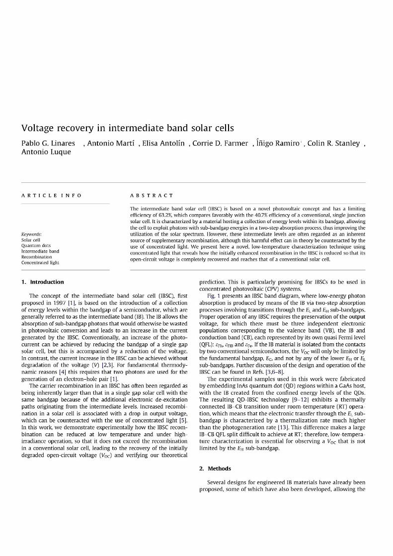
Two different types of solar cells were fabricated by molecular beam epitaxy (MBE) for this work: a 30 layer InAs/GaAs QD-IBSC and a GaAs reference solar cell (the control sample). A simple IBSC requires only an IB material sandwiched between p- and n-emitters for the exploitation of the full Voc potential. A detailed sketch of the layer structure of our QD-IBSC is presented in Fig. 2, together with the specifications of the composition, doping and thickness of each layer. The bottom layer consists of a 625 urn thick n-type GaAs wafer on top of which the device was grown. Next, a buffer layer was grown to smooth the surface. Then, an n + - Alo.2Gao.8As that acts as the n-emitter of the cell, was added.
tap 5 nm , rront
pCaAs ^ mic,i
window layer *"•
p - emitter
p++- GaAs (Be 2.5x 10>9 cm1) r sontad layer
30 X
¡Lift
BSF
baiter layer
rear metal
o--Alo.BoGaoaAs ÍBe5 x 10'°cm J :
p-GaAs (Be2x 1018cm'3)
'y :srj nm
H O MM
-S^. InAS QD (2.4 ML)
GaAs t f t
n* - AkzGaoaAs (Si 1 x 10,B cm"3)
rf -GaAs (Si 2 x 10'scm !)
2655 nrtt
high 7 spacer 75 nm
4.5+4.5 nm
N Si 6-doping 3 x HPcnV 3
200 nm
™„m
Substrate í n + -GaAs(Si2x10 , B cm") *\y
: . . : . . • - ^ ' . : o . M . - . .
Fig. 2. QD-IBSC layer structure including doping and thickness data for each layer. The IB region consists of 30 stacked QD layers, each of which is separated by a thick spacer, which incorporates the Si 8-doping.
The IB material was grown next and consists of 30 layers of self-assembled InAs QDs built up by Stranski-Krastanov growth and separated by thick, intrinsic GaAs spacers, which, as an alternative to the strain compensation technique [11,12], are meant to dilute the accumulated vertical strain and thus prevent dislocations. A large spacer thickness also prevents carrier tunneling between contiguous QD layers [14]. A quaternary Ino.2Alo.2Gao.6As capping was added to preserve the QD height/base aspect ratio, to red-shift the £H transition [26] and to eliminate the CB discontinuity with the GaAs barrier layer and thus, prevent the formation of an additional quantum well (QW) [27] in an effort to isolate the IB from the CB. Si 5-doping was included to half-fill the IB with electrons, so there are both empty states to enable the electrons to be pumped from the VB to the IB and filled states to assist in the IB-CB transition [8]. After the IB material region, a p-type GaAs emitter completes the electrically active part of the solar cell. Finally, an AlGaAs window, a p+-GaAs contact layer and an antireflective coating (ARC) complete the IBSC structure. The reference cell structure is identical except for the lack of the QD-IB region and the substitution of the n+-Al0.2Ga0.8As emitter by a 2 x 1017 cm"3 doped, 3.1 urn n-type base layer on top of a 200 nm n+-Alo.2Ga0.8As BSF layer. We will later discuss the impact of this substitution in the interpretation of our results.
3. Results and discussion
From detailed balance calculations at RT, the electrical behavior of both the IBSC and the reference cell operating at the radiative limit can be inferred (the sun is treated as a black body at 6000 K). At 1 sun operation, the IBSC efficiency is marginally higher than the reference cell efficiency (34.5% compared to 30.7%), assuming a fundamental bandgap of £G=1.42eV at RT and an IB located 0.3 eV below the CB, which is a realistic assumption for InAs/GaAs QD-IBSCs. However, under high irradiance, this same IBSC structure has a significantly higher potential than the reference cell, e.g., when both are operated at 1,000 suns, the IBSC efficiency limit is 47.2% compared to 35.8%. This
larger efficiency difference is caused by the more rapid increase of Voc for the IBSC compared to the reference cell, i.e., the reference cell Voc is approximately 150 mV higher than the IBSC V0c under 1 sun operating conditions, whereas the Voc difference decreases to 8 mV for a concentrated illumination of 1,000 suns.
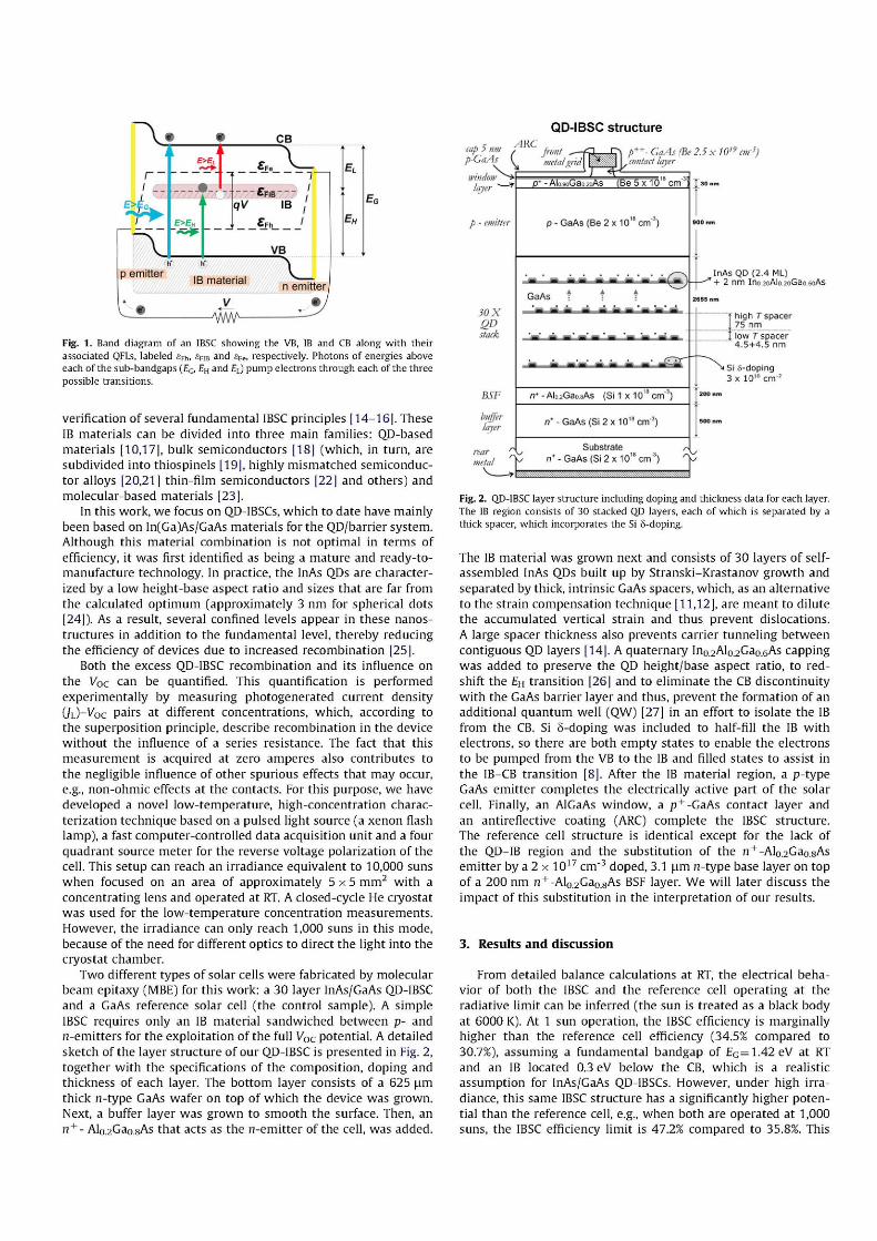
The dark curve of a solar cell provides an insight into the recombination taking place in the device. It is conventionally divided into two recombination regimes: the low-voltage regime, dominated by Shockley-Read-Hall recombination in the space-charge region and characterized by a low exponential slope in the range of e/2feT(i.e., an ideality factor m2 = 2); and the high-voltage regime, dominated by recombination in the neutral zones and characterized by an exponential slope of e/kT ( m ^ l ) at low injection. However, as shown in the detailed balance calculations of Fig. 3 (resulting in a purely m = l dark current), the electronic recombination of an IBSC differs from the conventional solar cell case. In black, solid lines, the dark current density (J)-V characteristics for both an IBSC (£G=1.42eV, £H = 1.12eV and £L=0.3eV) and its reference cell are represented. Within the low J range, up to ~ 1 mAcm~2, both curves remain parallel and are separated by a significant gap, i.e., the IBSC recombination is much larger because, even with the IB assumed thermally separated from the CB (and radiatively linked), it is dominated in this range by only one of the electronic transitions to or from the IB (D2 and D3 in the inset of Fig. 3). Between]=\ mAcm~2
and J =23 x 104 mAcm~2, an operating regime with a lower exponential slope (and influenced by the second of the electronic transitions to or from the IB) becomes dominant and leads to the recovery of V0o Above the current density of a typical GaAs solar cell operating under 1,000 suns illumination (2.5 x 10⁴ mA cm - 2 ) , the two recombination characteristics nearly converge, meaning that the VB-CB transition (Di in the inset) is now dominating the IBSC recombination, leading to the recovery of the IBSC Voc, as demonstrated experimentally in this work.
The JL-VOC characteristics of the IBSC and the reference cell calculated with the detailed balance model under illumination are represented as red, dashed curves in Fig. 3 for a broad range of concentrated light levels. TheseJL-V0c curves, which superimpose their respective dark characteristics (at least to a fairly accurate extent), are the ones that can be compared in practice for the analysis of the solar cell recombination, since the series resistance present in actual device dark curves would otherwise make the interpretation of the recombination difficult.
Detailed balance calculations 7r_,|=300 K
Voltage, V(V)
Fig. 3. Detailed balance J-V characteristics of an IBSC (£G=l-42 eV and £L=0.3 eV) and a conventional solar cell with the same bandgap. The dark J- V characteristics are represented by black solid lines, and the JL-V0c pairs are represented by red, dashed lines. The inset shows a simplified version of the IBSC electric equivalent circuit. (For interpretation of the references to colour in this figure legend, the reader is referred to the web version of this article.)
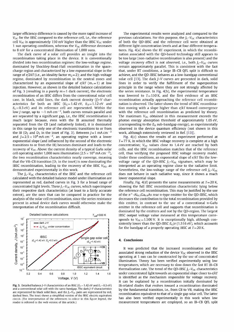
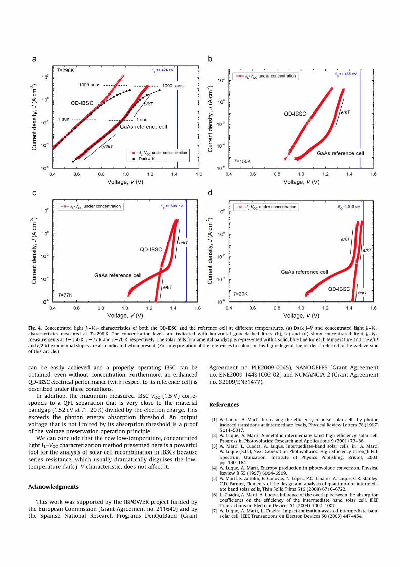
The experimental results were analyzed and compared to the previous calculations. For this purpose, the JL-Voc characteristics of both the QD-IBSC and the reference cell were obtained at different light concentration levels and at four different temperatures. Fig. 4(a) shows the RT experiment, in which the recombination associated with the QD-based technology still appears to be too large (non-radiative recombination is also present) and the voltage recovery effect is not observed, i.e., both JL-Voc curves remain approximately parallel. This is consistent with the fact that, under RT conditions, a large IB-CB QFL split is difficult to achieve, and the QD-IBSC behaves as a low-bandgap conventional solar cell [13]. The dark J-V curves are presented in dark, solid lines in order to verify the fulfillment of the superposition principle in the range where they are not strongly affected by the series resistance. In Fig. 4(b), the experimental temperature was lowered to r=150K, and the first evidence of an IBSC recombination actually approaching the reference cell recombination is observed. The latter shows the trend of IBSC recombination moving with a slope higher than e/kT toward convergence with the reference cell recombination as predicted by theory. The maximum V0c obtained in this measurement exceeds the photon energy absorption threshold of approximately 1.05 eV, (corresponding to the £H sub-bandgap energy), as experimentally observed in the device quantum efficiency (not shown in this work, although extensively reviewed in Ref. [13]).
Fig. 4(c) shows the results of an experiment performed at T= 77 K, in which the IBSC voltage recovery is complete at a high concentration; Voc values close to 1.4 eV are reached by both cells, and the IBSC recombination matches that of the reference cell, thus verifying the proposed IBSC voltage recovery model. Under these conditions, an exponential slope of e/kT fits the low-voltage range of the QD-IBSC JL-V0c signature, which may be interpreted as an operating regime close to the radiative limit. Nevertheless, the low-voltage range of the reference cell JL-Voc
does not behave in such radiative way, since it shows a much lower exponential slope.
Finally, Fig. 4(d) presents the same measurements at T=20 K, showing the full IBSC recombination characteristic lying below the reference cell recombination. This may be justified by the use of the n+-Al0.2Ga0.8As rear n-type emitter for the QD-IBSC, which decreases the contribution to the total recombination provided by this emitter, in contrast to the use of a conventional n-GaAs emitter in the reference cell and supports that recombination is dominated by the emitters and not by the QD-region. The largest IBSC output voltage value measured at this temperature corresponds to Voc=1.506 V. It is exceptionally high, although consistently lower than the QD-IBSC £G/e (1.516 eV), which accounts for the bandgap of a properly operating IBSC at T=20 K.
4. Conclusions
It was predicted that the increased recombination and the associated strong reduction of the device V0c observed in the IBSC operating at 1 sun can be counteracted by the use of concentrated illumination. Theory has been verified experimentally using low temperatures, which are necessary to slow down the fast RT IB-CB thermalization rate. The trend of the QD-IBSC JL-Voc characteristics under concentrated light towards an exponential slope closer to e/kT is identified as the mechanism responsible for voltage recovery. It can be explained by a recombination initially dominated by IB-related diodes that evolves toward a recombination dominated by the fundamental transition, i.e., from CB to VB, making the IBSC recombination equivalent to that of a single gap solar cell. The latter has also been verified experimentally in this work when low measurement temperatures are employed, so an IB-CB QFL split
a
10* r
E O < ID
S'
CD
Ü 10*
10°
T=298K
1000 suns J K
QD-IBSC
1000 suns
1 sun
GaAs reference cell
-x— JL- V^ under concentration
- • - D a r k J-V
0.4 0.6 OS 1.0 1.2
Voltage, V(V) 1.6
1 0 ' fc-
E o < 10°
£ i°-2
• o
O 10"" -
i o -
- x - J. - v „ under concentration £.= 1.485 eV
QD-IBSC
7=150K
GaAs reference cell
0.4 0.6 0.8 1,0 1.2
Voltage, V(V) 1.4 1 6
10'
E o ¿ 10°
c 10* CD l u
CD
E 10*
10°
-x—J.-V^ under concentration E =1.508 eV
QD-IBSC
GaAs reference eel!
7=77 K
e/kT
0.4 0.6 0.8 1.0 1.2
Voltage, V(V)
10* r
o < 10°
CD io-¿
3 ^ t
- x - J, - ^ under concentration
GaAs reference cell
F =1.518eV
7=20K
0.4 0.6 0.8 1.0 1.2
Voltage, V(V)
Fig. 4. Concentrated light JL-Voc characteristics of both the QD-IBSC and the reference cell at different temperatures, (a) Dark J-V and concentrated light JL-Voc characteristics measured at T=298 K. The concentration levels are indicated with horizontal gray dashed lines, (b), (c) and (d) show concentrated light JL-Voc measurements at T=150K, 1—11 KandT=20K, respectively. The solar cells fundamental bandgap is represented with a solid, blue line for each temperature and the ejkl and e/2 kT exponential slopes are also indicated when present. (For interpretation of the references to colour in this figure legend, the reader is referred to the web version of this article.)
can be easily achieved and a properly operating IBSC can be obtained, even without concentration. Furthermore, an enhanced QD-IBSC electrical performance (with respect to its reference cell) is described under these conditions.
In addition, the maximum measured IBSC Voc (1.5 V) corresponds to a QFL separation that is very close to the material bandgap (1.52 eV at T=20 K) divided by the electron charge. This exceeds the photon energy absorption threshold. An output voltage that is not limited by its absorption threshold is a proof of the voltage preservation operation principle.
We can conclude that the new low-temperature, concentrated light JL-VOC characterization method presented here is a powerful tool for the analysis of solar cell recombination in IBSCs because series resistance, which usually dramatically disguises the low-temperature dark J- V characteristic, does not affect it.
Acknowledgments
This work was supported by the IBPOWER project funded by the European Commission (Grant Agreement no. 211640) and by the Spanish National Research Programs DenQuIBand (Grant
Agreement no. PLE2009-0045), NANOGEFES (Grant Agreement no. ENE2009-14481C02-02) and NUMANCIA-2 (Grant Agreement no. S2009/ENE1477).
References
[1] A. Luque, A. Marti, Increasing the efficiency of ideal solar cells by photon induced transitions at intermediate levels, Physical Review Letters 78 (1997) 5014-5017.
[2] A. Luque, A. Marti, A metallic intermediate band high efficiency solar cell, Progress in Photovoltaics: Research and Applications 9 (2001) 73-86.
[3] A. Martí, L. Cuadra, A. Luque, Intermediate-band solar cells, in: A. Marti, A. Luque (Eds.), Next Generation Photovoltaics: High Efficiency through Full Spectrum Utilization, Institute of Physics Publishing, Bristol, 2003, pp. 140-164.
[4] A. Luque, A. Marti, Entropy production in photovoltaic conversion, Physical Review B 55 (1997) 6994-6999.
[5] A. Martí, E. Antolín, E. Cánovas, N. López, P.G. Linares, A. Luque, C.R. Stanley, CD. Farmer, Elements of the design and analysis of quantum-dot intermediate band solar cells, Thin Solid Films 516 (2008) 6716-6722.
[6] L. Cuadra, A. Marti, A. Luque, Influence of the overlap between the absorption coefficients on the efficiency of the intermediate band solar cell, IEEE Transactions on Electron Devices 51 (2004) 1002-1007.
[7] A. Luque, A. Martí, L. Cuadra, Impact-ionization-assisted intermediate band solar cell, IEEE Transactions on Electron Devices 50 (2003) 447-454.

[8] A. Martí, L. Cuadra, A. Luque, Partial filling of a quantum dot intermediate band for solar cells, IEEE Transactions on Electron Devices 48 (2001) 2394-2399.
[9] S.M. Hubbard, CD. Cress, C.G. Bailey, R.P. Raffaelle, S.G. Bailey, D.M. Wilt, Effect of strain compensation on quantum dot enhanced GaAs solar cells, Applied Physics Letters 92 (2008) 123512-1-123512-3.
[10] A. Luque, A. Martí, C.R. Stanley, N. López, L. Cuadra, D. Zhou, J.L. Pearson, A.J. McKee, General equivalent circuit for intermediate band devices: Potentials, currents and electroluminescence, Journal of Applied Physics 96 (2004) 903-909.
[11] R. Oshima, A. Takata, Y. Okada, Strain-compensated InAs/GaNAs quantum dots for use in high-efficiency solar cells, Applied Physics Letters 93 (2008) 083111-1-083111-3.
[12] V. Popescu, G.I. Bester, M.C. Hanna, A.G. Norman, A. Zunger, Theoretical and experimental examination of the intermediate-band concept for strain-balanced (In,Ga)As/Ga(As,P) quantum dot solar cells, Physical Review B 78 (2008) 205321-1-205321-17.
] 13] E. Antolin, A. Marti, CD. Farmer, P.G. Linares, E. Hernández, A.M. Sánchez, T. Ben, S.I. Molina, CR. Stanley, A. Luque, Reducing carrier escape in the InAs/ GaAs quantum dot intermediate band solar cell, Journal of Applied Physics 108 (2010) 064513-1-064513-7.
[14] E. Antolin, A. Marti, P.G. Linares, I. Ramiro, E. Hernández, CD. Farmer, CR. Stanley, A. Luque, Advances in quantum dot intermediate band solar cells, In: Proceedings of the 35th IEEE Photovoltaic Specialists Conference (PVSC), 2010, Honolulu, Hawaii, USA.
] 15] E. Antolin, A. Marti, J. Olea, D. Pastor, G. González-Díaz, I. Mártil, A. Luque, Lifetime recovery in ultrahighly titanium-doped silicon for the implementation of an intermediate band material, Applied Physics Letters 94 (2009) 1-3.
] 16] A. Marti, E. Antolin, CR. Stanley, CD. Farmer, N. López, P. Díaz, E. Cánovas, P.G. Linares, A. Luque, Production of Photocurrent due to Intermediate-to-Conduction-Band Transitions: A Demonstration of a Key Operating Principle of the Intermediate-Band Solar Cell, Physical Review Letters 97 (2006) 247701-247704.
[17] A. Martí, L. Cuadra, A. Luque, Quantum dot intermediate band solar cell, In: Proceedings of the 28th IEEE Photovoltaic Specialists Conference (PVSC), 2000, Glasgow, UK.
] 18] A. Luque, A. Marti, E. Antolin, C Tablero, Intermediate band versus levels in non-radiative recombination, Physica B 382 (2006) 320-327.
[19] P. Palacios, I. Aguilera, K. Sánchez, J.C Conesa, P. Wahnón, Transition-Metal-Substituted Indium Thiospinels as Novel Intermediate-Band Materials: Prediction and Understanding of Their Electronic Properties, Physical Review Letters 101 (2008) 046403-1-046403-4.
[20] N. López, L.A. Reichertz, K.M. Yu, K. Campman, W. Walukiewicz, Engineering the Electronic Band Structure for Multiband Solar Cells, Physical Review Letters 106 (2011) 028701-1-028701-4.
[21 ] W. Wang, A.S. Lin, J.D. Phillips, Intermediate-band photovoltaic solar cell based on ZnTe:0, Applied Physics Letters 95 (2009) 011103-1-011103-3.
[22) A. Martí, D. Fuertes Marrón, A. Luque, Evaluation of the efficiency potential of intermediate band solar cells based on thin-film chalcopyrite materials, Journal of Applied Physics 103 (2008) 1-6.
[23) N.J. Ekins-Daukes, T.W. Schmidt, A molecular approach to the intermediate band solar cell: The symmetric case, Applied Physics Letters 93 (2008) 063507-1-063507-3.
[24) P.G. Linares, A. Martí, E. Antolin, A. Luque, III—V compound semiconductor screening for implementing quantum dot intermediate band solar cells, Journal of Applied Physics 109 (2011) 014313-1-014313-8.
[25) A. Luque, P.G. Linares, E. Antolin, E. Cánovas, CD. Farmer, CR. Stanley, A. Marti, Multiple levels in intermediate band solar cells, Applied Physics Letters 96 (2010) 013501-1-013501-3.
[26] V.M. Ustinov, A.E. Zhukov, A.R Kovsh, N.A. Maleev, S.S. Mikhrin, A.F. Tsatsul'nikov, M.V. Maximov, B.V. Volovik, D.A. Bedarev, P.S. Kop'ev, Z.I. Alferov, L.E. Vorob'ev, D.A. Firsov, A.A. Suvorova, LP. Soshnikov, P. Werner, N.N. Ledentsov, D. Bimberg, Long-wavelength emission from self-organized InAs quantum dots on GaAs substrates, Microelectronics Journal 31 (2000) 1-7.
[27] P.G. Linares, CD. Farmer, E. Antolin, S. Chakrabarti, A.M. Sánchez, T. Ben, S.I. Molina, CR. Stanley, A. Marti, A. Luque, Inx(GayAll-y)l-xAs quaternary alloys for quantum dot intermediate band solar cells, Energy Procedía 2 (2010) 133-141.