Voltage Mode Inverter (VMI) Controller11 Continental Blvd Merrimack NH 03054 v. (603) 546-0090 f....
30
11 Continental Blvd Merrimack NH 03054 v. (603) 546-0090 f. (603)386- 6366 oztekcorp.com Voltage Mode Inverter (VMI) Controller User s Manual UM- 0037
Transcript of Voltage Mode Inverter (VMI) Controller11 Continental Blvd Merrimack NH 03054 v. (603) 546-0090 f....

11 Continental Blvd Merrimack NH 03054
v. (603) 546-0090 f. (603)386-6366 oztekcorp.com
Voltage Mode Inverter (VMI) Controller
User s Manual
UM-0037

About Oztek
Oztek Corp. is proven innovator of power, control, and instrumentation
solutions for the most demanding
industrial applications. Oztek
products include variable motor drives, grid tie inverters, frequency converters,
stand alone inverters, DC/DC converters, and DSP based control boards for power control applications.
Trademarks
OZDSP3000 is a trademark of Oztek Corp. Other trademarks, registered trademarks, and product names are the property of their respective owners and are used herein for identification purposes only.
Notice of Copyright
Oztek VMI
User s
Manual © December
2011
Oztek Corp. All rights reserved.
Exclusion for Documentation
UNLESS SPECIFICALLY AGREED TO IN WRITING, Oztek Corp. ( Oztek )
(A)
MAKES NO WARRANTY AS TO THE ACCURACY, SUFFICIENCY OR SUITABILITY OF ANY TECHNICAL OR OTHER INFORMATION
PROVIDED IN ITS MANUALS OR OTHER DOCUMENTATION.
(B)
ASSUMES NO RESPONSIBILITY OR LIABILITY FOR LOSSES, DAMAGES, COSTS OR EXPENSES, WHETHER SPECIAL, DIRECT, INDIRECT, CONSEQUENTIAL OR INCIDENTAL, WHICH MIGHT ARISE OUT OF THE USE OF SUCH INFORMATION. THE USE OF ANY SUCH
INFORMATION WILL BE ENTIRELY AT THE USER S RISK.
(C)
IF THIS MANUAL IS IN ANY LANGUAGE OTHER THAN ENGLISH, ALTHOUGH STEPS HAVE BEEN TAKEN TO MAINTAIN THE ACCURACY
OF THE TRANSLATION, THE ACCURACY CANNOT BE GUARANTEED. APPROVED OZTEK CONTENT IS CONTAINED WITH THE ENGLISH
LANGUAGE VERSION WHICH IS POSTED AT WWW.OZTEKCORP.COM.
Date and Revision
November
2012
Rev B
Part Number
UM-0037
Contact Information
USA Telephone: 603-546-0090
Fax: 603-386-6366
Email [email protected]

Publication UM-0037
i
Table of Contents
Table of Contents
1.
Introduction
.......................................................................................................................
4
1.1
Referenced Documents
...............................................................................................................
4
1.2
Definitions
....................................................................................................................................
4
2.
Functional Description
.......................................................................................................
5
2.1
Typical Hardware Implementation
..............................................................................................
5
2.1.1
Power Module
.........................................................................................................................
6
2.1.2
Pre-Charge Circuit
....................................................................................................................
6
2.1.3
Power Rectifier
........................................................................................................................
6
2.1.4
Output
Filter
............................................................................................................................
6
2.1.5
Isolation Transformer
..............................................................................................................
7
2.1.6
Current Sensors
.......................................................................................................................
7
2.1.6.1
Primary Current Sensors
.................................................................................................
7
2.1.6.2
Secondary Current Sensors
.............................................................................................
7
2.1.7
OZDSP3000 Controller
.............................................................................................................
7
2.2
Description of Operation
.............................................................................................................
7
2.3
State Sequencing
.........................................................................................................................
8
2.3.1
Initialize
...................................................................................................................................
9
2.3.2
Calibrate
..................................................................................................................................
9
2.3.3
Precharge
.................................................................................................................................
9
2.3.4
Charge
....................................................................................................................................
10
2.3.5
Idle
.........................................................................................................................................
10
2.3.6
On
..........................................................................................................................................
10
2.4
Precharge Process
......................................................................................................................
10
2.5
Fault and Warning Conditions
...................................................................................................
11
2.5.1
Warnings
................................................................................................................................
11
2.5.1.1
Local Bias Supply Tolerance Warnings
..........................................................................
12
2.5.1.2
DC Link High Voltage
.....................................................................................................
12
2.5.1.3
DC Link Low Voltage
......................................................................................................
12
2.5.1.4
Line Frequency Out of Tolerance
..................................................................................
12
2.5.1.5
Line Voltage Out of Tolerance
......................................................................................
12
2.5.1.6
Inverter & Cabinet High Temperature
..........................................................................
12
2.5.2
Faults
.....................................................................................................................................
12
2.5.2.1
Precharge Timeout Error
..............................................................................................
13
2.5.2.2
Precharge Contactor Error
............................................................................................
13
2.5.2.3
Line Contactor Error
......................................................................................................
13
2.5.2.4
Relay Driver Hardware Error
.........................................................................................
13
2.5.2.5
Configuration Memory Error
........................................................................................
13
2.5.2.6
Calibration Error............................................................................................................
14
2.5.2.7
DC Link Faults
................................................................................................................
14
2.5.2.8
Line Frequency Fault
.....................................................................................................
14
2.5.2.9
Line Voltage Fault
.........................................................................................................
14
2.5.2.10
Inverter Hardware Over-Temperature
.........................................................................
14
2.5.2.11
Inverter IGBT Error
........................................................................................................
14
2.5.2.12
Software Inverter Over-Temperature
...........................................................................
15
2.5.2.13
Output Overload
...........................................................................................................
15
2.5.2.14
Output Voltage
.............................................................................................................
15
3.
OZDSP3000 Hardware Interfacing
....................................................................................
16

ii
Table of Contents
VMI Controller User s Manual
3.1
Application Interfaces
................................................................................................................
16
3.1.1
J1/J2/J3: Auxiliary LEM Current Sensor Interfaces
................................................................
16
3.1.2
J4 Cabinet Temp Thermistor Interface
..................................................................................
17
3.1.3
J8: Relay Driver Interface
.......................................................................................................
17
3.1.4
J9: Contactor Status Feedback
..............................................................................................
17
3.1.5
J11/J13: SKiiP Power Module Interface
.................................................................................
18
3.1.6
Custom Driver Interface Considerations
...............................................................................
19
3.1.6.1
Power
............................................................................................................................
19
3.1.6.2
Switch Commands
........................................................................................................
19
3.1.6.3
Error Inputs
...................................................................................................................
19
3.1.6.4
DC Link Voltage Sensing
................................................................................................
20
3.1.6.5
DC Link Hardware Over-Voltage Protection
.................................................................
20
3.1.6.6
Hardware Over-Current and Desaturation Protection
.................................................
20
3.1.6.7
Current Sense Signals
....................................................................................................
20
3.1.6.8
Temperature Sense Signals
...........................................................................................
20
3.1.7
J20 Line Voltage Line Feedback
.............................................................................................
20
3.1.8
J23: High Voltage Line Feedback
...........................................................................................
21
3.1.9
P1 Isolated RS485 ModBus Interface
....................................................................................
21
3.1.10
J25: Bias Power Input
............................................................................................................
22
3.2
Electrical Interfaces
....................................................................................................................
23
3.3
Mechanical Interface
.................................................................................................................
24
4.
Maintenance and Upgrade
...............................................................................................
25
Warranty and Product Information
........................................................................................
26
Return Material Authorization Policy
.....................................................................................
28

Publication UM-0037
iii
Table of Contents
Table of Figures
Figure 1 -
Typical Single Phase VMI Configuration
........................................................................................
5
Figure 2 -
Typical Three Phase Isolated VMI Configuration
..........................................................................
5
Figure 3
Typical VMI Electrical System Schematic
.....................................................................................
6
Figure 4
VMI Controller Functional Block Diagram
....................................................................................
8
Figure 5
System State Machine
..................................................................................................................
9
Figure 6 -
Precharge Process Flowchart
......................................................................................................
11
Figure 7
OZDSP3000 VMI Application Electrical Connections
..................................................................
16
Figure 8
P1 Pinout -
RS422/485 Configuration
.........................................................................................
22
Figure 9
Approximate Connector, Jumper, LED, and Test Hook Locations
..............................................
23
Figure 10
OZDSP3000 Mechanical Dimensions
........................................................................................
24
Table of Tables
Table 1
J1/2/3 LEM Sensor Pin Assignments
............................................................................................
17
Table 2
J8 Relay Drive Pin Assignment
.....................................................................................................
17
Table 3
J9 Contactor Status Pin Assignment
............................................................................................
18
Table 4
J11/13 SKiiP Power Module Pin Assignment
...............................................................................
18
Table 5
J11 Current Sense Pin Assignment
..............................................................................................
20
Table 6
J20 High Voltage Line Sense Pin Assignment
...............................................................................
20
Table 7
J23 High Voltage Sense Pin Assignment
......................................................................................
21
Table 8
J15 RS422/485 Configuration Jumper Settings
............................................................................
21
Table 9
J12 RS-485 Pin Assignment
..........................................................................................................
22

VMI Controller User s Manual
4
Introduction
1.
Introduction
This document is intended to provide instruction on how to employ the Oztek Voltage Mode Inverter (VMI)
firmware application on a standard Oztek OZDSP3000 controller
in a hardware
system. It describes the electrical connections as well as the scaling of the various signals required by the control firmware.
1.1
Referenced Documents
Ref.
Document
Description
[1]
UM-0018
OZDSP3000 Users Manual
[2]
FS-0053
ModBus
Protocol Function Specification
[3]
FS-0054
VMI Modbus Communications Registers
[4]
UM-0015
Oztek TMS28x CAN Bootloader Users Manual
[5]
UM-0036
Power Control Center GUI User s Manual
1.2
Definitions
AFE Active Front End
CAN Controller Area Network
DSP Digital signal processor
EEPROM Electrically Erasable Programmable Read Only Memory
EMC Electro-magnetic compatibility
EMI Electro-magnetic interference
GND Ground, low side of input power supply
GTI Grid Tied Inverter
GUI Graphical User Interface
HMI Human Machine Interface
IPM Intelligent Power Module
N.C.
Not connected
PCB Printed Circuit Board
PCC Power Control Center
PLC Programmable Logic Controller
PLL Phase Locked Loop
POR Power On
Reset
PWM Pulse width modulation
SVM Space Vector Modulator
VMI Voltage Mode Inverter

Publication UM-0037
5
Functional Description
2.
Functional
Description
A Voltage Mode Inverter
is used to provide an AC
voltage source from an intermediate DC
circuit or Link. It can be used to produce AC power from variable power sources such as batteries, fuel cells, and windmills as well as convert from one type of AC power to another, i.e. frequency converter applications. Figure 1
and Figure 2
illustrate typical single and three phase
VMI hardware configurations.
Figure 1
-
Typical Single Phase VMI Configuration
Figure 2
-
Typical Three Phase Isolated VMI Configuration
2.1
Typical Hardware Implementation
An electrical system block diagram of a typical VMI 60Hz to 400Hz Frequency Converter application is presented in Figure 3. While component values will vary from application to application depending on
line voltage and power level, the overall system configuration will generally remain the same.
The three phase power is rectified and filtered to provide a DC Link voltage to the power converter. The main power converter is comprised of a three phase IGBT bridge whose output is then filtered and isolated by a transformer before being made available to the loads. A DSP control board is used to implement control of the 400Hz power electronics assembly while a PLC based HMI is provided for high level operation of the product.

VMI Controller User s Manual
6
Functional Description
Figure 3
Typical VMI Electrical System Schematic
2.1.1
Power Module
The power module is a three phase semiconductor bridge which controls the power transfer from the AC Line to the DC link
and vice versa. Oztek control boards are designed to interface directly with Semikron SKiiP power modules. In addition to the power devices, these modules provide current sensing, DC link
voltage sensing, temperature sensing, and protection features including over voltage, over current, and desaturation
protection.
2.1.2
Pre-Charge Circuit
A pre-charge circuit is used to limit the inrush current associated with charging the DC link
capacitance when applying line voltage to the VMI. Lack of a pre-charge
circuit can result in extremely high, potentially damaging inrush currents.
2.1.3
Power Rectifier
A three phase diode bridge is used to rectify the AC input into a DC Link voltage for the VMI frequency converter to operate off of. The rectifier is fed by a three phase contactor controlled by the control board firmware, allowing the firmware to pre-charge the DC Link.
2.1.4
Output Filter
A second order, three phase L-C filter is used to remove the PWM switching components from the switch-mode voltage output. Resistors and inductors are used in series with the capacitors to provide damping of resonances.

Publication UM-0037
7
Functional Description
2.1.5
Isolation Transformer
A three phase transformer is used to provide galvanic isolation and voltage translation on the output of the converter. In addition, the transformer s leakage inductance, together with additional discrete capacitors, forms a secondary output filter to help meet the output THD requirements.
2.1.6
Current Sensors
The VMI firmware expects to sense current both at the primary and secondary sides of the output transformer.
2.1.6.1
Primary Current Sensors
Primary current is sensed via current sensors incorporated in to the Power Modules.
2.1.6.2
Secondary Current Sensors
LEM type current sensors are included on the output of the transformer to provide feedback for controlling the magnetization current in the isolation transformer.
2.1.7
OZDSP3000 Controller
The OZDSP3000 is an Oztek off the shelf control solution intended for rapid prototyping and low volume production of power control systems. It has been designed to specifically interface with Semikron Power Modules and provides all of the necessary interfaces for controlling a VMI including isolated, high voltage line sensing, RS-485 communication port, relay drivers etc.
2.2
Description of Operation
Figure 4
presents a simplified block diagram of the control scheme employed in the VMI firmware. This block diagram illustrates the controls for a single output phase. Each phase is independently controlled allowing the controller to operate in single or multiphase applications. The voltage controller is a resonant mode
type regulator whose reference sets the value of the output voltage. This reference is adjusted by the line drop compensator to account for IR drops in long output cable runs. The adjusted reference is then compared to the measured output
voltage providing
the voltage error input to the resonant mode controller.
The output
of the voltage controller is adjusted by a DC Link Voltage feed forward term, limited, and
used to control a pulse width modulator
which generates the gating commands to the power switches.

VMI Controller User s Manual
8
Functional Description
Figure 4
VMI Controller Functional Block Diagram
2.3
State Sequencing
A state machine is used to provide deterministic control and sequencing of the VMI hardware. If a fault is detected in any of the operating states, the
hardware
is
placed into a safe condition and the state machine is latched into the Fault state. Figure 5
illustrates the operating states as well as the transition logic employed in the system state machine.

Publication UM-0037
9
Functional Description
Figure 5
System State Machine
2.3.1
Initialize
The state machine resets to the Initialize
state following a power-on-reset (POR) event. While in this state the power hardware is not operable; the firmware is initializing hardware
peripherals, configuring variables, and
performing self health tests. Upon successful
initialization the state machine will auto-transition to the Calibrate
state.
2.3.2
Calibrate
The Calibrate
state is used to calibrate system hardware as applicable.
Power hardware is not operable
while in the Calibrate
state. Following successful
calibration, the state machine will auto-transition to the Precharge
state.
2.3.3
Precharge
The Precharge
state is used to wait for a valid AC line
interface before attempting to begin the DC link
charging process. The state machine will remain in the Precharge
state indefinitely,
VMI Controller User s Manual
10
Functional Description
transitioning either on a fault or upon detecting a valid AC line.
Power hardware is not
operable
while in the Precharge
state.
2.3.4
Charge
The Charge
state is used to charge the DC link
capacitance in a controlled manner before
directly connecting to the AC line. Once the DC link
is charged, the state machine will sequence
to the Idle
state. Power hardware is not operable
while in the Charge
state.
2.3.5
Idle
Once in the Idle
state the VMI is ready for use. The state machine will remain in the Idle
state indefinitely, transitioning either on a fault, a turn-on command, or upon detecting an
invalid AC line.
2.3.6
On
While in the On
state the VMI is processing power and will remain in the On
state indefinitely, transitioning either on a fault or a turn-off command.
2.4
Precharge Process
The application software is capable of controlling external precharge components for use in precharging the DC Link capacitors from the AC line.
Figure 6
illustrates the logic used to implement the precharge process.

Publication UM-0037
11
Functional Description
Figure 6
-
Precharge Process Flowchart
2.5
Fault and Warning Conditions
The VMI provides warning indicators and fault protection in the event of conditions that may cause damage to the equipment or injure personnel. The various conditions that are monitored by the VMI are listed and described in the following sections.
2.5.1
Warnings
The VMI provides the warning indicators listed below. These warning conditions do not prohibit operation of the VMI; they are merely reported for informational purposes only.

VMI Controller User s Manual
12
Functional Description
2.5.1.1
Local Bias Supply Tolerance Warnings
The VMI firmware monitors the local bias supplies (24V, 15V, 5V, 3.3V, and -15V) on the control board and will set a warning flag if the corresponding supply voltage is not within the range required by the on-board hardware. The various warning flags will remain set while the supply voltages are out of tolerance and will be cleared when the supply is found to be within the required limits.
2.5.1.2
DC Link High Voltage
The VMI firmware monitors the DC link voltage and will set a warning flag if it exceeds the DC Link Over-Voltage Warning Threshold
configuration parameter. This flag will remain set until the voltage falls below the DC Link Over-Voltage Recover Threshold
configuration parameter.
2.5.1.3
DC Link Low Voltage
The VMI firmware monitors the DC link voltage and will set a warning flag if it falls below the DC Link Under-Voltage Warning Threshold
configuration parameter. This flag will remain set until the voltage exceeds the DC Link Under-Voltage Recover Threshold
configuration parameter.
2.5.1.4
Line Frequency Out of Tolerance
The VMI firmware monitors the AC Line frequency and will set a warning flag if it falls below the AC Line
Low Frequency Warning Threshold
or exceeds the
AC Line
High Frequency Warning Threshold
configuration parameters. These
flags
will remain set until the frequency
exceeds the AC Line
Low Frequency Recover Threshold
or the AC Line
High Frequency Recover Threshold
configuration parameters respectively.
2.5.1.5
Line Voltage Out of Tolerance
The VMI firmware monitors the AC Line voltage and will set a warning flag if it falls below the AC Line
Low Voltage Warning Threshold
or exceeds the AC Line
High Voltage Warning Threshold
configuration parameters. These flags
will remain set until the voltage exceeds the AC Line
Low Voltage Recover Threshold
or the AC Line
High Voltage Recover Threshold
configuration parameters respectively.
2.5.1.6
Inverter & Cabinet High Temperature
The VMI firmware monitors the inverter power module and cabinet temperatures and will set warning flags if they exceed
the Inverter Temperature Warning Threshold
or Cabinet
Temperature Warning Threshold
configuration parameters. These
flags
will remain set until the temperature falls below the
Inverter Temperature Recover Threshold
or Cabinet
Temperature Recover Threshold
configuration parameters respectively.
2.5.2
Faults
The VMI provides the fault protection listed below. Whenever a fault occurs the VMI will automatically turn the converter OFF, open the main line contactor and transition to the FAULT state.

Publication UM-0037
13
Functional Description
The controller remains in the FAULT state and the latched fault flags remain set until explicitly reset with a
Fault Reset
command. This is true even if the source(s) of the
fault(s) are no longer
active.
Upon receiving the Fault Reset
command, the VMI will attempt to clear all latched fault
bits. It then examines the sources of all fault conditions and if none are active the VMI controller will transition to the Precharge state. If upon re-examination any sources of faults are still active, their respective fault flags are latched again and the VMI will remain in the FAULT state.
2.5.2.1
Precharge Timeout Error
The VMI Firmware monitors the amount of time spent in the CHARGE State. A fault will be asserted if the DC Link Precharge Enable
configuration parameter is set to TRUE (i.e. the VMI is controlling the precharge function) and the elapsed time exceeds the Precharge Timeout Threshold configuration parameter.
2.5.2.2
Precharge Contactor Error
The VMI monitors the status of the precharge contactor feedback signal if the precharge contactor monitor is enabled in the Contactor Monitor Enables
configuration parameter. If, after the time specified in the Contactor Debounce Time
configuration parameter has passed, the precharge contactor is not in the state commanded by the VMI, a fault will be asserted.
2.5.2.3
Line Contactor Error
The VMI monitors the status of the main line contactor feedback signal if the line contactor monitor is enabled in the Contactor
Monitor Enables
configuration parameter. If, after the time specified in the Contactor Debounce Time
configuration parameter has passed, this contactor is not in the state commanded by the VMI, a fault will be asserted.
2.5.2.4
Relay Driver Hardware Error
The VMI
monitors the status of the relay drive circuit on the control board that is used to drive the precharge and main line contactors. This hardware circuit provides the ability to detect open load, short circuit, over-voltage and over-current conditions. A fault is asserted if any of these conditions are reported.
2.5.2.5
Configuration Memory Error
This fault occurs any time a read from the configuration memory is performed and the CRC for the block being read does not match the CRC stored in the memory. This may occur if the data was corrupted in transmission during the read or this may occur if the data stored in memory was corrupted. Unlike all other fault sources, this fault condition is not cleared with the Fault Reset
command as the fault condition indicates the possibility that the control parameters are not as intended. Instead, this fault is considered a major system fault and needs to be addressed as follows:
1.
Attempt to reload the system configuration using the Configuration Reload
command or cycle power to the control board. Either of these actions will reset the CPU on the control board which then forces a re-initialization of the application, including reading the configuration parameters from the external configuration memory. If this

VMI Controller User s Manual
14
Functional Description
completes without error, this implies the previous error occurred while the data was being read.
2.
If after executing step 1 above a configuration error is still present, this may indicate bad data in the configuration memory. In this case, the memory will need to be reset to the factory defaults using the Configuration Reset
command. Once the memory contents
have been reset and any values changed to their customized settings, step 1 above should be executed to force a reload of the system variables.
3.
If neither of the above result in clearing the configuration error, then there is likely an issue with the control board hardware. At this point the board should be sent back to the factory for diagnosing and repairing of any defects (see the RMA process described at the end of this document).
2.5.2.6
Calibration Error
When first powering up the control board the VMI software attempts to calibrate the controller s internal ADC. This error is asserted if the controller is unable to perform the required calibration. There is likely an issue with the control board hardware if this error occurs, in which case the board should be sent back to the factory for diagnosing and repairing of any defects (see the RMA process described at the end of this document).
2.5.2.7
DC Link Faults
The VMI firmware monitors the DC link voltage and will assert a fault if it exceeds the DC Link Over-Voltage Fault Threshold or falls below the
DC Link Under-Voltage Fault Threshold
configuration parameters.
2.5.2.8
Line Frequency Fault
The VMI firmware monitors the AC Line frequency and will assert a fault if it exceeds the AC Line Frequency High
Fault Threshold or falls below the
AC Line Frequency Low
Fault Threshold
configuration parameters.
2.5.2.9
Line Voltage Fault
The VMI firmware monitors the AC Line voltage and will assert a fault if it exceeds the AC Line Voltage High
Fault Threshold or falls below the
AC Line Voltage Low
Fault Threshold
configuration parameters.
2.5.2.10
Inverter Hardware Over-Temperature
The VMI firmware provides a means to recognize a hardware-based over-temperature error signal
from the inverter interface (as is present on a typical Semikron SKiiP interface).
2.5.2.11
Inverter IGBT Error
The VMI firmware provides a means to recognize a hardware-based IGBT error signal from the inverter interface (as is present on a typical Semikron SKiiP interface).

Publication UM-0037
15
Functional Description
2.5.2.12
Software Inverter Over-Temperature
The VMI monitors the inverter and cabinet temperatures and will assert a fault if they exceed
the Inverter Temperature Fault Threshold
or the Cabinet
Temperature Fault Threshold
configuration parameters respectively.
2.5.2.13
Output
Overload
The VMI firmware monitors the RMS output
current for each of the three phases and asserts
a
fault if any phase exceeds the Output
Over-Current Fault Threshold
configuration parameter.
2.5.2.14
Output Voltage
The VMI firmware monitors the RMS output voltage for each of the three phases and asserts a fault if any phase exceeds the Output
Over-Voltage Fault Threshold
or falls below the Output
Under-Voltage Fault Threshold
configuration parameters.
VMI Controller User s Manual
16
OZDSP3000 Hardware Interfacing
3.
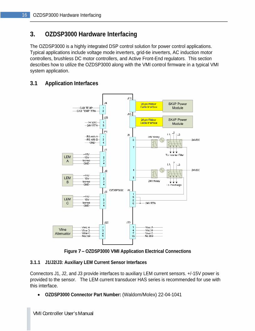
OZDSP3000 Hardware Interfacing
The OZDSP3000 is a highly integrated DSP control solution for power control applications. Typical applications include voltage mode
inverters, grid-tie inverters, AC induction motor
controllers, brushless DC motor controllers, and Active Front-End regulators. This section describes how to utilize the OZDSP3000
along with the VMI control firmware in a typical VMI
system application.
3.1
Application
Interfaces
Figure 7
OZDSP3000 VMI Application Electrical Connections
3.1.1
J1/J2/J3: Auxiliary LEM Current Sensor Interfaces
Connectors J1, J2, and J3 provide interfaces to auxiliary LEM current sensors. +/-15V power is provided to the sensor. The LEM current transducer HAS series is recommended for use with this interface.
OZDSP3000 Connector Part Number:
(Waldom/Molex) 22-04-1041

Publication UM-0037
17
OZDSP3000 Hardware Interfacing
Mating Connector Part Number: (Waldom/Molex) 22-01-1042
Input Range: +/-
4V
Table 1
J1/2/3
LEM Sensor
Pin Assignments
J1/2/3
Pin #
Description
1
+15V
2
-15V
3
Iout
4
Iout Return
3.1.2
J4 Cabinet Temp Thermistor Interface
Connector J4 provides an interface for a 10k cabinet thermistor style temperature sensor.
OZDSP3000 Connector Part Number:
(Molex) Micro-Fit 2 Position
Header: 43650-0215
Mating Connector Part Number: (Molex) Micro-Fit 2 Position
Receptacle:
43645-0200
Input Range: 0 to open circuit
3.1.3
J8: Relay Driver Interface
The VMI firmware automatically controls both a pre-charge relay as well as a line interface relay, intended to drive the coils of higher power contactors.
Table 2
J8 Relay Drive Pin Assignment
Pin #
Description
3
Line interface relay 24V drive
7
Line interface relay drive return
4
Pre-charge relay 24V drive
8
Pre-charge relay drive return
OZDSP3000 Connector Part Number:
(Molex) Micro-Fit 2x4 Header: 43045-0824
Mating Connector Part Number: (Molex) Micro-Fit 2x4 Receptacle: 43025-0800
Output Range: 24V, 2A continuous, 5A inrush
3.1.4
J9: Contactor Status Feedback
The VMI firmware expects switch closure feedback from both the pre-charge as well as the line interface contactors. These switch closure, status feedback signals should be wired to the opto-coupler inputs on J9, as illustrated in Figure 7.

VMI Controller User s Manual
18
OZDSP3000 Hardware Interfacing
Table 3
J9 Contactor Status Pin Assignment
Pin #
Description
1
Pre-charge contactor status (switched 24V)
5
24V Return
2
Line contactor status (switched 24V)
6
24V Return
OZDSP3000 Connector Part Number:
(Molex) Micro-Fit 2x4 Header: 43045-0824
Mating Connector Part Number:
(Molex) Micro-Fit 2x4 Receptacle: 43025-0800
Input Range: Logic high: 0V or floating. Logic low: 3V
25V
3.1.5
J11/J13:
SKiiP Power Module Interface
Connector J11 provides an interface to SKiiP style Semikron power modules. This interface complies with Semikron s required specifications. The OZDSP3000 supplies 24V power to the power module via pins 14 and 15. PWM commands (15V logic level) are supplied to the top and bottom switches of each of the three half bridges via signals INV_TOP_U(V,W) and INV_BOT_U(V,W) respectively. Feedback of phase currents, temperature, and DC link
voltage are provided on INV_IOUT_U(V,W), INV_TEMP, INV_UDC signals respectively. Error signals from the module are similarly provided via INV_ERR_U(V,W) and INV_OVT. Please refer to the Semikron datasheet for the particular module being used for more information.
Table 4
J11/13
SKiiP Power Module
Pin Assignment
Pin #
Description
1
Ground
2
INV_BOT_U
(Phase A)
3
INV_ERR_U
(Phase A)
4
INV_TOP_U (Phase A)
5
INV_BOT_V (Phase B)
6
INV_ERR_V
(Phase B)
7
INV_TOP_V (Phase B)
8
INV_BOT_W (Phase C)
9
IN_ERR_W
(Phase C)
10
INV_TOP_W
(Phase C)
11
INV_OVR_TEMP
12
n/c
13
INV_UDC
14
24V
15
24V
16
n/c
17
n/c
18
Ground

Publication UM-0037
19
OZDSP3000 Hardware Interfacing
Pin #
Description
19
Ground
20
INV_TEMP
21
INV_IOUT_U_RTN (Phase A)
22
INV_IOUT_U
(Phase A)
23
INV_IOUT_V_RTN
(Phase B)
24
INV_IOUT_V
(Phase B)
25
INV_IOUT_W_RTN
(Phase C)
26
INV_IOUT_W
(Phase C)
OZDSP3000 Connector Part Number:
(AMP) 499922-6
Mating Connector Part Number: (AMP) 1658621-6
Power:
24V @ 1.5A
3.1.6
Custom Driver Interface Considerations
When attempting to use the OZDSP3000 VMI controller with a custom designed power stage the hardware must be designed to provide the appropriate signals expected at the J11/13
interface. Generally some sort of custom printed circuit board will be required to interface the J11/13
signals to the gate drivers, current sensors, etc.
3.1.6.1
Power
The OZDSP3000 supplies 24V on J11/13, pins 14 & 15. This 24Vmay be used to power the electronics on the interface board. The supply is capable of providing 1.5A.
3.1.6.2
Switch Commands
The six switching commands are provided on pins 2, 4, 5, 7, 8, and 10. These switch command signals are driven off of the OZDSP3000 at 15V logic level using MC14504B level shifting devices.
3.1.6.3
Error Inputs
The OZDSP3000 expects three logic level, error inputs; one associated with each phase, on pins 3, 6, and 9. When active, these inputs cause the VMI firmware to latch the system off into the Fault state. Pull-ups
to 3.3V are provided on board and the signals are active high. Depending on the features provided in the custom design, these signals can be used to interface single error sources, multiple protection circuits, or none at all.
The custom interface board should drive the pin with an open-collector style circuit. In the case where no protection is provided, the pins should be grounded to disable the faults.

VMI Controller User s Manual
20
OZDSP3000 Hardware Interfacing
3.1.6.4
DC Link Voltage Sensing
The OZDSP3000 expects a signal proportional to DC link
voltage to be provided on J11, pin 13
with respect to pins 18 and 19. This signal should be scaled such that 0-10 V represents the measurable DC link
voltage range.
3.1.6.5
DC Link Hardware Over-Voltage Protection
When designing a custom interface it is highly recommended that hardware over voltage protection be implemented. This can be implemented with a comparator using the DC link
voltage sense output. The output of this comparator can be used to gate off the switch commands as well as assert the Error inputs on each phase.
3.1.6.6
Hardware Over-Current and Desaturation Protection
Semikron SKiiP power modules provide fast hardware over current and desaturation protection. When designing a custom power solution, these additional protection features should also be considered. When including over current, desaturation, and over voltage protection into the design, the fault flags must be logically ORd together and
reported using the open collector Error signal inputs to the OZDSP3000.
3.1.6.7
Current Sense Signals
The OZDSP3000 expects to receive a current sense signal for each half bridge phase output. This should be a bipolar signal where +/-10V corresponds to the full scale current range. The current sense signals should be provided on the following pins:
Table 5
J11 Current Sense Pin Assignment
J11 Pin #
Description
22
Current Phase A (U)
21
Gnd Reference for Current Phase A (U)
24
Current
Phase B (V)
23
Gnd Reference for Current Phase B (V)
26
Current Phase C (W)
25
Gnd Reference for Current Phase C (W)
3.1.6.8
Temperature Sense Signals
The OZDSP3000 expects to receive a 0-10V temperature signal
on pin 20
that corresponds to the hot spot temperature of the power devices.
3.1.7
J20 Line Voltage Line Feedback
The VMI firmware expects to sense AC line voltage on J20. This is a low voltage interface and requires an off-board attenuator.
Table 6
J20 High Voltage Line Sense Pin Assignment
J20 Pin #
Description
2
Line Voltage Phase A
3
Line Voltage Phase B

Publication UM-0037
21
OZDSP3000 Hardware Interfacing
J20 Pin #
Description
4
Line Voltage Phase C
5
Neutral
OZDSP3000 Connector Part Number:
(Molex) Micro-Fit 6 Header: 43650-0615
Mating Connector Part Number:
(Molex) Micro-Fit 6 Receptacle: 43645-0600
3.1.8
J23: High Voltage Line Feedback
The VMI firmware expects to sense output
voltage
for feedback control purposes
on J23. The standard hardware variant is designed to accept 115VAC voltages directly. Interfacing to other AC voltages may require a modification to the gain of the
sense amplifier (consult Oztek
for more information).
Table 7
J23 High Voltage Sense
Pin Assignment
Pin #
Description
1
Output
Voltage Phase A
4
Output
Voltage Phase B
7
Output
Voltage Phase C
10
Neutral
OZDSP3000 Connector Part Number:
(Waldom/Molex) 26-60-4100
Mating Connector Part Number:
(Tyco) 3-644465-7
3.1.9
P1 Isolated RS485 ModBus Interface
Connector P1 provides an isolated RS422/485 communications interface. In RS422/485 mode jumper block J15 is used to select between the two protocols and configure termination if desired as detailed in
Table 8. Figure 8Figure 8
illustrates the pinout of the connector in the RS422/485 configuration.
OZDSP2000 Connector Part Number:
(AMP) 747844-5
Mating Connector Part Number:
Industry Standard DB9 Male
Table 8
J15 RS422/485 Configuration Jumper Settings
Mode
Jumper 1-2
Jumper 3-4
Jumper 5-6
Jumper 7-8
RS422
TX Termination
RX Termination
DNP DNP RS485 Four-Wire
TX Termination
RX Termination
DNP DNP RS485 Two-Wire
Termination
DNP Connect TX to RX
Connect TX to RX

VMI Controller User s Manual
22
OZDSP3000 Hardware Interfacing
G
Pin 7
R
Pin 2
Pin 8
Pin 3
Pins 4-6
G
Pin 7
R
Pin 2
Pins 4-6
RS422 and RS485 Four-Wire
RS485 Two-Wire
Figure 8
P1 Pinout -
RS422/485 Configuration
3.1.10
J25: Bias Power Input
The OZDSP3000 requires 24VDC power input on terminal block J25. Note that Pin 3 is used for SPI boot enable;
it should be left floating or connected to ground for normal Flash Boot operation.
Table 9
J12 RS-485 Pin Assignment
Pin #
Description
1
24 VDC
5
24V Return
OZDSP3000 Connector Part Number:
(Phoenix Contact) 1733606
Mating Connector Part Number: n/a (terminal block style)
Voltage:
24V nominal, 18V min, 28V max
Current:
4.5A maximum (Inrush current while powering three SKiiP modules)

Publication UM-0037
23
OZDSP3000 Hardware Interfacing
3.2
Electrical Interfaces
The approximate location of the connectors, jumper blocks, LEDs, and test hooks are illustrated in Figure 9.
Figure 9
Approximate Connector, Jumper, LED, and Test Hook Locations

VMI Controller User s Manual
24
OZDSP3000 Hardware Interfacing
3.3
Mechanical Interface
Figure 10
OZDSP3000 Mechanical Dimensions

Publication UM-0037
25
Maintenance and Upgrade
4.
Maintenance and Upgrade
The firmware image on
the OZDSP3000
can be upgraded in-system
using the resident CAN
bootloader. For detailed information on how to upgrade the firmware or directly interface with the bootloader, please reference UM-0015 Oztek TMS28x CAN Bootloader Users Manual.

VMI Controller User s Manual
26
Warranty and Return
Warranty and Product Information
Limited Warranty
What does this warranty cover and how long does it last? This Limited Warranty is provided by Oztek Corp. ("Oztek") and covers defects in workmanship and materials in your OZDSP3000
controller. This Warranty Period lasts for 18 months
from the date of purchase at the point of sale to you, the original end user customer, unless otherwise agreed in writing. You will be required to demonstrate proof of purchase to make warranty claims. This Limited Warranty is transferable to subsequent owners but only for the unexpired portion of the Warranty Period. Subsequent owners also require original proof of purchase as described in "What proof of purchase is required?"
What will Oztek do? During the Warranty Period Oztek will, at its option, repair the product (if economically
feasible) or replace the defective product free of charge, provided that you notify Oztek of the product defect within the Warranty Period, and provided that through inspection Oztek establishes the existence of such a defect and that it is covered by this Limited Warranty.
Oztek will, at its option, use new and/or reconditioned parts in performing warranty repair and building replacement products. Oztek reserves the right to use parts or products of original or improved design in the repair or replacement. If Oztek repairs or replaces a product, its warranty continues for the remaining portion of the original Warranty Period or 90 days from the date of the return shipment to the customer, whichever is greater. All replaced products and all parts removed from repaired products become the property of Oztek.
Oztek covers both parts and labor necessary to repair the product, and return shipment to the customer via an
Oztek-selected non-expedited surface freight within the contiguous United States and Canada. Alaska, Hawaii and locations outside of the United States and Canada are excluded. Contact Oztek Customer Service for details on freight policy for return shipments from excluded areas.
How do you get service? If your product requires troubleshooting or warranty service, contact your merchant. If you are unable to contact your merchant, or the merchant is unable to provide service, contact Oztek directly at:
USA Telephone: 603-546-0090
Fax: 603-386-6366
Email [email protected]
Direct returns may be performed according to the Oztek Return Material Authorization Policy described in your product manual.
What proof of purchase is required? In any warranty claim, dated proof of purchase must accompany the product and the product must not have been disassembled or modified without prior written authorization by Oztek. Proof of purchase may be in any one of the following forms:
The dated purchase receipt from the original purchase of the product at point of sale to the end user
The dated dealer invoice or purchase receipt showing original equipment manufacturer (OEM) status
The dated invoice or purchase receipt showing the product exchanged under warranty

Publication UM-0037
27
Warranty and Return
What does this warranty not cover? Claims are limited to repair and replacement, or if in Oztek's discretion that is not possible, reimbursement up to the purchase price paid for the product. Oztek will be liable to you only for direct damages suffered by you and only up
to a maximum amount equal to the purchase price of the product.
This Limited Warranty does not warrant uninterrupted or error-free operation of the product or cover normal wear and tear of the product or costs related to the removal, installation, or troubleshooting of the customer's electrical systems. This warranty does not apply to and Oztek will not be responsible for any defect in or damage to:
a) The product if it has been misused, neglected, improperly installed, physically damaged or altered, either internally or externally, or damaged from improper use or use in an unsuitable environment
b) The product if it has been subjected to fire, water, generalized corrosion, biological infestations, or input voltage that creates operating conditions beyond the maximum or minimum limits listed in the Oztek
product specifications including high input voltage from generators and lightning strikes
c) The product if repairs have been done to it other than by Oztek
or its authorized service centers (hereafter "ASCs")
d) The product if it is used as a component part of a product expressly warranted by another manufacturer
e) The product if its original identification (trade-mark, serial number) markings have been defaced, altered, or removed
f) The product if it is located outside of the country where it was purchased
g) Any consequential losses that are attributable to the product losing power whether by product malfunction, installation error or misuse.
Disclaimer
Product
THIS LIMITED WARRANTY IS THE SOLE AND EXCLUSIVE WARRANTY PROVIDED BY OZTEK IN CONNECTION WITH YOUR OZTEK PRODUCT AND IS, WHERE PERMITTED BY LAW, IN LIEU OF ALL OTHER WARRANTIES, CONDITIONS, GUARANTEES,
REPRESENTATIONS, OBLIGATIONS AND LIABILITIES, EXPRESS OR IMPLIED, STATUTORY OR OTHERWISE IN CONNECTION WITH THE
PRODUCT, HOWEVER ARISING (WHETHER BY CONTRACT, TORT, NEGLIGENCE, PRINCIPLES OF MANUFACTURER'S LIABILITY,
OPERATION OF LAW, CONDUCT, STATEMENT OR OTHERWISE), INCLUDING WITHOUT RESTRICTION ANY IMPLIED WARRANTY OR CONDITION OF QUALITY, MERCHANTABILITY OR FITNESS FOR A PARTICULAR PURPOSE. ANY IMPLIED WARRANTY OF
MERCHANTABILITY OR FITNESS FOR A PARTICULAR PURPOSE TO THE EXTENT REQUIRED UNDER APPLICABLE LAW TO APPLY TO THE PRODUCT SHALL BE LIMITED IN DURATION TO THE PERIOD STIPULATED UNDER THIS LIMITED WARRANTY.
IN NO EVENT WILL OZTEK BE LIABLE FOR: (a) ANY SPECIAL, INDIRECT, INCIDENTAL OR
CONSEQUENTIAL DAMAGES, INCLUDING
LOST PROFITS, LOST REVENUES, FAILURE TO REALIZE EXPECTED SAVINGS, OR OTHER COMMERCIAL OR ECONOMIC LOSSES OF ANY
KIND, EVEN IF OZTEK HAS BEEN ADVISED, OR HAD REASON TO KNOW, OF THE POSSIBILITY OF SUCH DAMAGE, (b) ANY LIABILITY ARISING IN TORT, WHETHER OR NOT ARISING OUT OF OZTEK'S NEGLIGENCE, AND ALL LOSSES OR DAMAGES TO ANY PROPERTY
OR FOR ANY PERSONAL INJURY OR ECONOMIC LOSS OR DAMAGE CAUSED BY THE CONNECTION OF A PRODUCT TO ANY OTHER DEVICE OR SYSTEM, AND (c) ANY DAMAGE OR INJURY ARISING FROM OR AS A RESULT OF MISUSE OR ABUSE, OR THE INCORRECT
INSTALLATION, INTEGRATION OR OPERATION OF THE PRODUCT. IF YOU ARE A CONSUMER (RATHER THAN A PURCHASER OF THE PRODUCT IN THE COURSE OF A BUSINESS) AND PURCHASED THE
PRODUCT IN A MEMBER STATE OF THE EUROPEAN UNION, THIS LIMITED WARRANTY SHALL BE SUBJECT TO YOUR STATUTORY
RIGHTS AS A CONSUMER UNDER THE EUROPEAN UNION PRODUCT WARRANTY DIRECTIVE 1999/44/EC AND AS SUCH DIRECTIVE HAS
BEEN IMPLEMENTED IN THE EUROPEAN UNION MEMBER STATE WHERE YOU PURCHASED THE PRODUCT. FURTHER, WHILE THIS
LIMITED WARRANTY GIVES YOU SPECIFIC LEGAL RIGHTS, YOU MAY HAVE OTHER RIGHTS WHICH MAY VARY FROM EU MEMBER STATE TO EU MEMBER STATE OR, IF YOU DID NOT PURCHASE THE PRODUCT IN AN EU MEMBER STATE, IN THE COUNTRY
YOU PURCHASED THE PRODUCT WHICH MAY VARY FROM COUNTRY TO COUNTRY AND JURISDICTION TO JURISDICTION.

VMI Controller User s Manual
28
Warranty and Return
Return Material Authorization Policy
Before returning a product directly to Oztek
you must obtain a Return Material Authorization (RMA) number and
the correct
factory "Ship To" address. Products must also be shipped prepaid. Product shipments will be refused
and returned at your
expense if they are unauthorized,
returned without an RMA
number clearly marked on the
outside of the shipping box, if they
are shipped collect, or if they are shipped to the wrong location.
When you contact Oztek
to obtain service, please have your instruction manual ready for reference and be
prepared to
supply:
The serial number of your product
Information about the installation and use of the unit
Information about the failure and/or reason for the return
A copy of your dated proof of purchase
Return Procedure
Package the unit safely, preferably using the original box and packing materials. Please ensure that your product is shipped
fully insured in the original packaging or equivalent. This warranty will not apply where the product is damaged due to
improper packaging.
Include the following:
The RMA number supplied by Oztek
clearly marked on the outside of the box.
A return address where the unit can be shipped. Post office boxes are not acceptable.
A contact telephone number where you can be reached during work hours.
A brief description of the problem.
Ship the unit prepaid to the address provided by your Oztek
customer service representative.
If you are returning a product from outside of the USA or Canada -
In addition to the above, you MUST include
return freight funds and you are fully responsible for all documents, duties, tariffs, and deposits.
Out of Warranty Service
If the warranty period for your product has expired, if the unit was damaged by misuse or incorrect installation, if other
conditions of the warranty have not been met, or if no dated proof of purchase is available, your unit may be serviced or
replaced for a flat fee.
If a unit cannot be serviced due to damage beyond salvation or because the repair is not economically
feasible, a labor fee may still be incurred
for the time spent making this determination.
To return your product for out of warranty service, contact Oztek
Customer Service for a Return Material Authorization
(RMA) number and follow the other steps
outlined in "Return Procedure".
Payment options such as credit card or money order will be explained by the Customer Service Representative. In cases where
the minimum flat fee does not apply, as with incomplete units or units with excessive damage, an additional fee will be
charged. If applicable, you will be contacted by Customer Service once your unit has been received.