VLSI SOC Design ET4351
40
1 VLSI SOC Design ET4351 Rene van Leuken EWI/MECE/CAS http://ens.ewi.tudelft.nl/Education/courses/et4351/index.php http://ens.ewi.tudelft.nl/Education/msc_projects.php
Transcript of VLSI SOC Design ET4351

1
VLSI SOC Design ET4351
Rene van Leuken
EWI/MECE/CAS
http://ens.ewi.tudelft.nl/Education/courses/et4351/index.php
http://ens.ewi.tudelft.nl/Education/msc_projects.php
2
Goal
• The aim is of the course is to address important aspects of SoC design methodology issues. Including: 1) Algorithm to specification 2) Low power digital design issues, 3) On-chip system IP high level interconnect issues, 4) Hardware <-> software interaction issues
• Synthesis based digital design from a language description: SystemC, SystemC-AMS, C++, VHDL, …
• Prototyping in FPGA boards
• Semi-custom VLSI design (UMC, TSMC)

3
Content
• Topics covered among other: optimization and reduction techniques, Low power interconnect, SoC design methodology, modelling, specification and implementation, communication architecture and protocols.
• Keywords: 2 process design style, loops, interconnect, timing, SystemC, VHDL, High Level synthesis, ASIC design

4
Web Server
• All information is on:
ens.ewi.tudelft.nl/Education/courses/et4351

5
Books i
• Understanding Behavioral Synthesis, A practical Guide to High-Level Design, John P. Elliot, Kluwer Academic Publishers Study material - ISBN: 079238542X
• Digital Systems Design with VHDL and Synthesis: An Integrated Approach, KC Chang ISBN: 0769500234

6
Books ii
• Low-Power Electronics Design by Christian Piguet (Editor), ISBN: 0849319412
• Essential VHDL - RTL Synthesis Done Right, by Sundar Rajan ISBN: 0966959000
• A SystemC Primer, J. Bhasker, ISBN 0-9650391-8-8

7
Schedule 2016
Introduction/content
Low power design, communication
SystemC, C++, Examples
SystemC TLM and SystemC AMS
Structured VHDL design, loops
Communication, busses, Wishbone (AXI), NoC
Timing & ASIC flow (Cadence, Synopsys, Vivado)
Introduction and division of projects

8
Our architecture
Instruction program bus peripheral
processor
DSP/Computeblock

Soc: Block schema
sys_ctrl
mbl1c_core
IMEM
DMEM
wb_slaveaddress_decoder
mst_wb_adapter
wb_SoC
wb_mbl1c

10
Communication: Wishbone

11
Wishbone timing

04/10/12 12
Projecting the future
Sept. 10, 2009 PATMOS 2009 12

3D stack of MPSoc and NoC's

14
TSV 3D chips

Circuits and Systems
3D Stacking
IBM 2012

Circuits and Systems
MPSoC Architecture
� 2D or 3D, architectural challenges are
similar
� Raw execution performance:
–Task scheduling/mapping/load-balancing –
where to execute what, and when
� Memory Hierarchy:
–What data to keep on-chip?
–How to improve the efficiency of on-chip
caches?
� Interconnect:
–How to reduce transfer latency, maintain
high throughput
–How to build in adaptability, redundancy,
security


18
Projects i
• All tasks have the goal to design and simulate some hardware
function, part of a SoC, and possibly to test functionality on
the Spartan 3/6/ZED board.
• Language: VHDL or SystemC (C++)
• Exercises are grouped around the Xilinx MicroBlaze SoC
and the Avnet Spartan 3/6/ZED board.
• Three themes: DSP (Image) and communication.
• Students grouped evenly for the themes!

19
Projects ii• All tasks /themes are the ‘same’
• Start with an algorithm, e.g. C Code or Matlab
• Design an hardware architecture; in VHDL or SystemC
• Your datapath
• Wishbone interface
• Power saving method?
• All modules will have a Wishbone bus interface
• Verify/simulate your design; Use the bus emulator package, download from website;
• Synthesize your design
• In case IO theme: program FPGA and check communication
• Write report.

20
Theme Image
• Gray scale image operations
• C code template code from “Practical algorithms for images analyses”, Michael Seul.
• Image binarization.
• Integer or fixed-point operations.

21
Image picture

Otsu's method is used to automatically perform clustering-based image thresholding or, the reduction of a graylevel image to a binary image. The algorithm assumes that the image to be thresholded contains two classes of pixels or bi-modal histogram.
Otsu's Algorithm
AlgorithmCompute histogram and probabilities of each intensity level
Set up initial and
Step through all possible thresholds maximum intensity
Update and Compute
Desired threshold corresponds to the maximum
You can compute two maxima (and two corresponding thresholds).

C/C++ designs using ViVado HLS

C/C++ designs
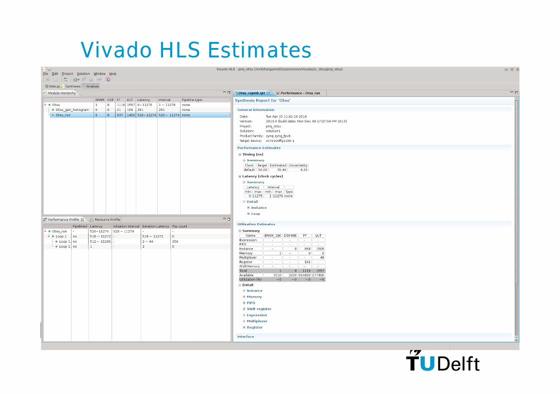
Vivado HLS Estimates

Vivado HLS Scheduling

27
Project ASIC
ASIC (semi custom) realization of a chip.
Existing VHDL code of a design: Xilinx MicroBlaze
Use Synopsys Design compiler and Cadence SoC Encounter.
The goal is to 'map' the filter design to a semi-custom cell library (Faraday SP90) and by using SOCE place and route the design.
Design steps include: simulation, synsthesis (DC), IO port design, power planning, clocktree generation, P&P and GDS2 (SOCE) generation.
The result is a GDS2 file, which in principle could be fabricated at a silicion foundry.

The power plan of the ASIC. Rings, stripes,block halo and the selected floorplaning are visible

View of the routed, verified and finalized ASIC

30
UMC 90nm Realization

31
LowPower async 8051

32
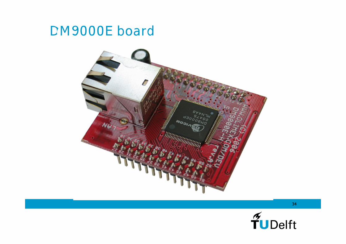
Project Communication
• Communication interface processor.
• Ethernet: DM9000E
• High level communication chips.
• VHDL and embedded C - and Host processor C code.
• (This year: fingerprint sensor interface)

33
FPGA board: Spartan 3
http://www.em.avnet.com
34
DM9000E board

DM9000E video

36
Projects Procedure
• Select a topic and discuss it with me
• Design the IP block (hardware/software)
• Result = simulation, or in some cases implementation in
FPGA, C code software
• Write report: what/why/how/results. This typically a 4 to 10
page report.

37
Reactions 1This labwork was much bigger and took much more time than I expected it to do. On the web site of the course an estimation of 20 hours is given, and I thought that I would have needed at least twice as much. I turned out it took much longer than my own estimates. This might be due to the fact that I worked alone. Besides the fact that it took a lot longer than expected, I really enjoined the work itself. It gave me huge satisfaction to see that at the end it was working well. I was also talking one day with a man that is Computer Engineer in Italy, and we came in the discussion about this labwork I was doing and it was very pleasant to hear that this is the kind of work that he sometimes has to do in real life. It gave me the feeling that all the courses and professors are really preparing me for a job or research. I learned a lot during this lab course. First of all I had never programmed in VHDL on such high level. I learned a lot about VHDL and about approaching such an assignment. I also learned much about the Wishbone bus interface and about C, for example about arithmetic and logical shifts in C. I learned also a lot about simulating with Modelsim and synthesizing with Synplify Pro. It will certainly be useful in the future to know my way around in these programs. Last but not least, I think I learned again to hold on. At some times I thought I would never finish the job, and the strange values in the simulation kept coming. I learned that I could do it if I just hold on and tried to debug it by looking in completely other ways at my design. I think this will be the most valuable lesson for the future.

38
Reactions 2In the end we can say that the project went quite well. The assignment was clear and we were able to formulate a concept in the first meeting. Once we fully understood the SoC templates we started coding our bridge module. After successfully simulating our design we tidied up our code to include our latest VHDL coding ideas. We experienced some trouble creating the bit file, but once we got the latest ISE we were in business and able to test our design on the development board. Our first try was not completely right but after some puzzling we realized that we did not map the reset functionality.The second try was successful. We both experienced this small project as a welcome exercise for our digital design and VHDL coding skills.

39
Reactions 3We really liked working on this project, because we both are very interested in (embedded) hardware/software co-design. This project also master VHDL a lot more. We were already experienced with VHDL, but by doing projects of this size one gains more experience.The project took us a lot more time than the 20 prescribed hours (multiples of it), but because we liked the subject we didn’t careabout that too much. Although we would have liked it to test the design on our Spartan-3E (XC3S500E) FPGA boards, we couldn’t find the time to do this.

Success
Have Fun!!