
VLSI Design of a Processor for Discrete Wavelet Packet and ...
18
International Journal of Computing and Digital Systems ISSN (2210-142X) Int. J. Com. Dig. Sys. 10, No.1 (Jan-2021) E-mail: [email protected], [email protected], [email protected], [email protected], [email protected] http://journals.uob.edu.bh VLSI Design of a Processor for Discrete Wavelet Packet and Hilbert Transforms Peter Yusuf Dibal 1 , Elizabeth N. Onwuka 2 , James Agajo 3 , Caroline O. Alenoghena 2 and Achonu Adejo 2 1 Computer Engineering Department, University of Maiduguri, Maiduguri, Nigeria 2 Telecommunications Engineering Department, Federal University of Technology Minna, Minna, Nigeria 2 Computer Engineering Department, Federal University of Technology Minna, Minna, Nigeria Received 12 Mar. 2020, Revised 31 Jul. 2020, Accepted 5 Aug. 2020, Published 1 Jan. 2021 Abstract: Very Large Scale Integration (VLSI) design is a technological advancement in electronics that has widely shortened the window from concept to a working prototype in any design. It has also made it possible to design and develop sophisticated and intelligent electronic systems which are easily adaptable to any field of human endeavor with relative ease. In this paper, the VLSI design of a processor system is presented, which implements two transforms i.e. the discrete wavelet packet, and the Hilbert transforms. The combination of these two transforms in a single processor makes it possible to have a system with enhanced sub- band frequency edge detection in a wideband signal and other specialized areas, which is very useful in such specialized areas of application as spectrum sensing in cognitive radio networks. The results obtained from the simulation and design verification of the processor system showed the effectiveness of the design methodology presented in this paper. As a matter of fact, the arithmetic operators designed in this paper outperformed the arithmetic operators of the Xilinx IP CORE when compared in terms of speed. From the results obtained, it was clear that the processor design performed as expected, at a great speed. Keywords: Processor, Discrete Wavelet Packet Transform, Hilbert Transforms, FIR Filter, Lifting Steps 1. INTRODUCTION Processor design is important in the electronics world; it makes it possible to design and develop electronic systems and devices, which have practical and viable applications in solving real-life problems. The design approach for processors varies based on the expected functionality of the processor. It could range from simple, medium, to complex processors. Also, depending on the level of complexity of the processor, the associated tools for the design vary in sophistication. Simple and medium range processors usually perform a limited number of tasks, and are thus said to be application-specific, while the complex range processors perform a large number of tasks, which spread across different applications, and are thus said to be non- application-specific. This paper focuses on the design of a processor of the medium range category, which will be used to perform Discrete Wavelet Packet Transform (DWPT) function enhanced with a Hilbert transform (HT). The output of the DWPT stage of the design will be enhanced for better signal representation by passing it through a Hilbert transform stage. We refer to our work in [1] for exactly how this enhancement is achieved mathematically. To realize the objective of this paper, two design approach will be used. The first design approach is the lifting step, which will be used in the processor-design- implementation of the DWPT transform. The second design approach is the Finite Impulse Response (FIR) filter design, which will be used to perform the processor-design-implementation of the Hilbert transform. As stated earlier, the tools employed in the design of processors vary in sophistication and level of complexity. For the design in this paper, the tool of choice is the VHSIC (Very High Speed Integrated Circuit) Hardware Description Language (VHDL). VHDL is a powerful, independent, portable, and reusable language, which is used in the design of medium to complex range processors [2]. It allows the description of the behavior of an electronic device from which the physical circuit can be realized. Further information on VHDL can be found in [3]–[5]. Once the circuit is realized, it can then be implemented on a Complex http://dx.doi.org/10.12785/ijcds/100109
Transcript of VLSI Design of a Processor for Discrete Wavelet Packet and ...

International Journal of Computing and Digital Systems ISSN (2210-142X)
Int. J. Com. Dig. Sys. 10, No.1 (Jan-2021)
E-mail: [email protected], [email protected], [email protected], [email protected], [email protected]
http://journals.uob.edu.bh
VLSI Design of a Processor for Discrete Wavelet Packet
and Hilbert Transforms
Peter Yusuf Dibal1, Elizabeth N. Onwuka
2, James Agajo
3, Caroline O. Alenoghena
2
and Achonu Adejo2
1 Computer Engineering Department, University of Maiduguri, Maiduguri, Nigeria
2Telecommunications Engineering Department, Federal University of Technology Minna, Minna, Nigeria 2Computer Engineering Department, Federal University of Technology Minna, Minna, Nigeria
Received 12 Mar. 2020, Revised 31 Jul. 2020, Accepted 5 Aug. 2020, Published 1 Jan. 2021
Abstract: Very Large Scale Integration (VLSI) design is a technological advancement in electronics that has widely shortened the
window from concept to a working prototype in any design. It has also made it possible to design and develop sophisticated and
intelligent electronic systems which are easily adaptable to any field of human endeavor with relative ease. In this paper, the VLSI
design of a processor system is presented, which implements two transforms i.e. the discrete wavelet packet, and the Hilbert
transforms. The combination of these two transforms in a single processor makes it possible to have a system with enhanced sub-
band frequency edge detection in a wideband signal and other specialized areas, which is very useful in such specialized areas of
application as spectrum sensing in cognitive radio networks. The results obtained from the simulation and design verification of the
processor system showed the effectiveness of the design methodology presented in this paper. As a matter of fact, the arithmetic
operators designed in this paper outperformed the arithmetic operators of the Xilinx IP CORE when compared in terms of speed.
From the results obtained, it was clear that the processor design performed as expected, at a great speed.
Keywords: Processor, Discrete Wavelet Packet Transform, Hilbert Transforms, FIR Filter, Lifting Steps
1. INTRODUCTION
Processor design is important in the electronics
world; it makes it possible to design and develop
electronic systems and devices, which have practical and
viable applications in solving real-life problems. The
design approach for processors varies based on the
expected functionality of the processor. It could range
from simple, medium, to complex processors. Also,
depending on the level of complexity of the processor,
the associated tools for the design vary in sophistication.
Simple and medium range processors usually perform a
limited number of tasks, and are thus said to be
application-specific, while the complex range processors
perform a large number of tasks, which spread across
different applications, and are thus said to be non-
application-specific. This paper focuses on the design of
a processor of the medium range category, which will be
used to perform Discrete Wavelet Packet Transform
(DWPT) function enhanced with a Hilbert transform
(HT). The output of the DWPT stage of the design will
be enhanced for better signal representation by passing it
through a Hilbert transform stage. We refer to our work
in [1] for exactly how this enhancement is achieved
mathematically.
To realize the objective of this paper, two design
approach will be used. The first design approach is the
lifting step, which will be used in the processor-design-
implementation of the DWPT transform. The second
design approach is the Finite Impulse Response (FIR)
filter design, which will be used to perform the
processor-design-implementation of the Hilbert
transform. As stated earlier, the tools employed in the
design of processors vary in sophistication and level of
complexity. For the design in this paper, the tool of
choice is the VHSIC (Very High Speed Integrated
Circuit) Hardware Description Language (VHDL).
VHDL is a powerful, independent, portable, and reusable
language, which is used in the design of medium to
complex range processors [2]. It allows the description of
the behavior of an electronic device from which the
physical circuit can be realized. Further information on
VHDL can be found in [3]–[5]. Once the circuit is
realized, it can then be implemented on a Complex
http://dx.doi.org/10.12785/ijcds/100109

86 Peter Yusuf Dibal, et. al.: VLSI Design of a Processor for Discrete Wavelet Packet…
http://journals.uob.edu.bh
Programmable Logic Device (CPLD) or Field
Programmable Gate Array (FPGA). In this paper, the
target device is an FPGA.
A. Review of Related Works in Wavelet Processor
Design
Quite a number of research has been done in the
development of processors for wavelet transforms; the
authors in [6] proposed a wavelet processor based on the
lifting scheme that had no multipliers but with reduced
complexity, it however has low efficiency in area
requirements. An efficient dual mode Integer Haar
Lifting Wavelet Transform (IHLWT) was proposed in
[7], which had reduced requirements by exploiting
arithmetic operations redundancies involved with
IHLWT computations; the architecture was also
multiplier-free and performed IHLWT with a single
adder and subtractor. In [8], the authors proposed a DWT
architecture based on word serial pipeline and parallel
filter processing in which high and low-pass filters were
used concurrently at each level; this approach made the
design work twice faster than most traditional designs.
Using residue number system, the authors in [9] proposed
the design of a 2-dimensional DWT processor. A
symmetric extension scheme was employed by the design
to reduce distortion at image boundaries.
B. Review of Related Works in Hilbert Transform
Processor Design
In the design of Hilbert transform processors, authors
have used different approaches to realize their objectives.
As an example, the authors in [9] proposed a low power
and fast reconfigurable Hilbert transform processor based
on ripple carry adder and carry save adder thereby
bypassing multipliers; power reduction was achieved by
turning off adders when the multiplier operands were
zero. Using fast Fourier transform (FFT), the authors in
[10] designed a HT processor by multiplication with +j
and –j in the frequency domain; an efficient signal flow
graph was developed in the design by utilizing
decimation-in-frequency and decimation-in-time
approach. For approximations in image applications
based on HT, the authors in [11] proposed a model that
exploited the symmetry and alternating zero-valued
coefficients of an HT-FIR filter in the generation of in-
phase and quadrature components that were essential for
envelope computation. The target FPGA for their design
was the Stratix IV FPGA on a Terasic DE4-230 board.
The authors implemented a hardware for computing the
instantaneous frequency of a phonocardiogram using
discrete HT. Their design involved the use of a system
level modeling tool for DSP, a System Generator
provided by Xilinx in Simulink to achieve a faster design
cycle. The results obtained from their design were similar
to those computed using MATLAB.
The rest of this paper is organized as follows: we
review in section 2, the DWPT and the mechanism by
which it decomposes a signal alongside an analysis of the
DWPT lifting steps. Section 3 presents the
implementation of the floating point arithmetic
operations that will be used in the lifting steps; the
implementation involves the use of logic gates and
buffers. In section 4, the Hilbert transform is presented
with its design using FIR filter technique; in section 5, a
complex finite-state-machine (CFSM) design of the
wavelet processor stage is shown; the design in this
section is based on the lifting steps in section 2. Section 6
presents the design of the Hilbert transformer stage of the
processor; this section builds on section 4 and also
utilizes a CFSM in the design, while section 7 presents
the simulation of the designs made, the verification of the
designs, and also performance measurement. Finally, a
conclusion is presented in section 8.
2. DISCRETE WAVELET PACKET
TRANSFORM (DWPT)
In signal processing, DWPT belongs to the category
of wavelet transforms. It operates by representing known
and unknown signal features through wavelet basis.
DWPT can be viewed as a generalization of the wavelet
transform, and it uses filter banks arranged in a tree
structure format when implementing a wavelet algorithm.
A typical example of a DWPT tree is shown in Fig.
1[12], where the decomposition of a signal is
implemented by a low-pass (H) and high-pass filter (G)
pairs i.e. H-G pairs. Each parent node decomposing an
input signal in Fig. 1 is split into two subspaces jnW ,
which has the property of orthogonality, and is
mathematically expressed as:
, 2 , 1 2 1, 1n j n j n jW W W (1)
where n is a nonnegative integer, j is the decomposition
level, and is orthogonal addition. The wavelet packet
coefficients2
1[ ]
pl n
are generated using the scaling filter,
and the coefficients2 1
1[ ]
pl n
are generated using the
wavelet filter. The coefficients are mathematically
expressed as [12]:
21 2 [ ] 2 , 0,1,..., 1p p
l lk
n h k n k n N (2)
2 11 2 2 , 0,1,2,..., 1p p
l lk
n g k n k n N (3)
where kh is the low-pass filter, kg is the high-pass
filter, and p is the position at level l. For the signal in
each subband channel, the energy is calculated as [13]–
[15]:

Int. J. Com. Dig. Sys. 10, No.1, 85-102 (Jan-2021) 87
http://journals.uob.edu.bh
2
, , , ,
0 0
1T
j k j k j k j kj j k
E c t d dtT
(4)
2 2, ,
0
1j k j k
j j k
E c dT
(5)
where cj,k is scaling function coefficient, dj,k is the
wavelet function coefficient.
Figure 1. Analysis filter bank of a wavelet packet
According to [16], the decomposition functions in (2)
and (3) can be factored into lifting steps for an orthogonal
Daubechies wavelet with 4 vanishing moments (Db4) as
shown below in (6):
1
1
1 1 1
1 1 1
2 1 1
1 1 1
21 1
11 1
2 3 2 1
1 12 1 3 3 2 1
4 4
1
3 1
2
3 1
2
j jj
jj j j
j j j
j j
j j
s n s n s n
d n s n s n s n
s n s n d n
s n s n
d n d n
(6)
where 1js n is the updated value at the next iteration
(H filter output of Fig. 1), and 1jd n is the predicted
value at the next iteration (G filter output in Fig. 1). The
lifting steps in (6) is the basis by which the DWPT stage
of the processor will be designed, and its close inspection
reveals that the incoming signal js n is composed of
several data points upon which the lifting steps act to
achieve discrete wavelet packet transformation of the
incoming signal.
For the design in this paper, each of these data points
will be represented using the IEEE-754 single precision
floating point representation. The IEEE-754 single
precision floating point representation of numbers is a
32-bit format representation, consisting of 1-bit sign
representation, 8-bit exponent representation, and 23-bit
mantissa representation. The structure of the IEEE-754
single precision floating point format is shown in Fig.
2[17].
Figure 2. IEEE-754 floating point single precision data format
As an example of this data format, we present in
Table 1, the IEEE-754 single precision floating point
representation for three samples of an input data.
TABLE I. IEEE-754 SINGLE PRECISION FLOATING POINT DATA
REPRESENTATION
S/N Input
Data
IEEE-754 single precision floating point
representation
1 0.5377 00111111000010011010011010110101 2 1.8339 00111111111010101011110100111100 3 -2.2588 11000000000100001001000000101110
A. Analysis of DWPT Lifting Steps
A close inspection of (6) reveals that there are three
fundamental arithmetic operations involved in the
realization of the lifting steps. These are: multiplication,
addition, and subtraction. Owing to the IEEE-754 single
precision floating point representation of the data points
in js n , the arithmetic operations will be floating point
in nature; thus the multiplication operation will be IEEE-
754 single precision floating point multiplication, the
addition will be IEEE-754 single precision floating point
addition, and the subtraction will be IEEE-754 single
precision floating point subtraction.
To perform floating point multiplication on a pair of
32-bit numbers A and B using the structure shown in Fig.
2, different operations are performed on the constituent
parts of the numbers i.e. sign bit, exponent bits, and
mantissa bits [18], [19]. We propose the algorithm to
achieve this multiplication in Algorithm 1, where s1, e1,
and m1 are the sign bit, exponential bits, and mantissa
bits of the first number A, and s2, e2, and m2 are the sign
bit, exponential bits, and mantissa bits of the second
number B.

88 Peter Yusuf Dibal, et. al.: VLSI Design of a Processor for Discrete Wavelet Packet…
http://journals.uob.edu.bh
Algorithm 1: IEEE-754 Floating Point Unit Multiplier Algorithm
1 Initialize s1, e1, m1, s2, e2, m2, overflow 2 XOR [ s1, s2 ] product_sign_bit 3 Add [ e2, (e1 – 127) ] product_exponent 4 Append [ 1 , m1 ] intermediate_m1 5 Append [1 , m2 ] intermediate_m2 6 Multiply [ intermediate_m1, intermediate_m2 ] product_mantissa 7 If product_exponent > 255
8 1 Assert overflow
9 2 Product_sign_bit final_sign_bit 10 3 Assert final_product(30 down to 0)
11 4 Append [ final_sign_bit , final_product(30 down to 0) ] final_product(31 down to 0) 12 End
13 If product_mantissa(47) == 1
14 1 product_mantissa(46 downto 24) normalized_mantissa 15 2 Add [ 1, product_exponent ] final_exponent 16 3 Append [ product_sign_bit, final_exponent, normalized_mantissa ] final_product(31 down to 0) 17 Else
18 1 Product_mantissa( 45 downto 23 ) normalized_mantissa 19 2 Append [ product_sign_bit, product_exponent, normalized_mantissa ] final_product(31 down to 0) 20 End
For floating point addition and subtraction, operations
will also be performed on the sign bit, exponential bits,
and mantissa bits of both numbers A and B [19], [20].
We propose the algorithm shown in Algorithm 2 which is
used to achieve floating point addition and subtraction.
Algorithm 2: IEEE754 - Floating Point Unit Addition and Subtraction Algorithm
1 Initialize s1, e1, m1, s2, e2, m2 31 Begin: mantissaProcess 2 If e1 == e2 32 If xor ( s1, s2 ) == 0
3 1 Jump to mantissaProcess 33 1 Add ( m1, m2 ) Result_mantissa 4 End 34 2 OR ( s1, s2 ) Result_sign 5 If e1 > e2 35 Else if ( m1 >= m2 )
6 1 Sub ( e1, e2 ) exp_diff 36 1 Sub ( m1, m2 ) Result_mantissa 7 2 If exp_diff > 23 37 2 s1 Result_sign 8 1 Result_mantissa m1 38 Else if ( m1 < m2 )
9 2 Result_sign s1 39 1 Sub ( m2, m1 ) Result_mantissa 10 3 Result_exponent e1 40 2 s2 Result_sign 11 4 Jump to exitProcess 41 End if
12 3 Else 42 End: mantissaProcess
13 1 m2 ( 24 downto exp_diff ) m2
(exp_diff downto 0 )
43 If ( Result_mantissa == 0 )
14 2 0 m2 ( 24: sub ( 25, exp_diff ) ) 44 1 0 Result_mantissa 15 3 Jump to mantissaProcess 45 2 0 Result_exponent 16 4 End if 46 3 Jump to exitProcess
17 End if 47 Else if ( Result_mantissa(24) == 1 )
18 If e2 > e1 48 1 Append (0, Result_mantissa(24:1) Result_mantissa 19 1 Sub ( e2, e1 ) exp_diff 49
20 2 If exp_diff > 23 50 2 Add ( exponent, 1 )
21 1 Result_mantissa m2 51 3 Jump to exitProcess
22 2 Result_sign s2 52 Else if ( Result_mantissa(23) == 0 )
23 3 Result_exponent e2 53 1 Begin loop for j from 0 to 22
24 4 Jump to exitProcess 54 1 If Result_mantissa(j) == 1
25 3 Else 55 1 Result_mantissa(j+1:0)
Result_mantissa(24: sub(23, j) 26 1 m1 ( 24 downto exp_diff ) m1
(exp_diff downto 0 )
56
27 2 0 m2 ( 24: sub ( 25, exp_diff ) ) 57 2 0 Result_mantissa(22-j: 0) 28 3 Jump to mantissaProcess 58 3 (Result_exponent – 23) + j
Result_exponent 29 4 End if 59
30 End if 60 2 End if
61 2 End loop
62 End if
63 Begin: exitProcess 64 1 Result_sign final_result(31) 65 2 Result_exponent final_result(30:23) 66 3 Result_mantissa(22:0) final_result (22:0) 67 End: exitProcess

Int. J. Com. Dig. Sys. 10, No.1, 85-102 (Jan-2021) 89
http://journals.uob.edu.bh
3. IMPLEMENTATION OF LIFTING STEPS USING
FLOATING POINT ARITHMETIC
The lifting steps in (6), consists of three fundamental
arithmetic operations which are multiplication, addition,
and subtraction. All these operations are floating point in
nature due to the data representation of the incoming
signal. To design the architecture of the processor based
on this lifting steps, it is important to analyze the lifting
steps in details, and this done as follows:
The first line in the lifting steps involves splitting
the incoming signal values into even and odd
components based on their index values. Each
odd-indexed signal values are then multiplied by
the square root of 3 and then added to the even
values to get the first preliminary “update” value
of the lifting step.
In the second line of the lifting steps, we multiply
the updated values in (i) above by a factor of
3 4 and subtract the product from the odd-
indexed signal values in the original signal. We
also multiply the unit delayed values of the
updated values in (i) above by a factor of
3 2 4 and then subtract the product from
the odd-indexed signal values in the original
signal. The final result is the first preliminary
“predict” value of the lifting step.
In the third line of the lifting step, we compute
the difference between the first preliminary
updated values and the first preliminary predicted
values to obtain the second preliminary updated
values.
The fourth line of the lifting step involves the
multiplication of the second preliminary “update”
values by a factor of 3 1 2 to obtain the
final “update” values for the current level of
iteration.
In the fifth line of the lifting scheme, the first
preliminary “predict” value is multiplied by a
factor of 3 1 2 to obtain the final
“predict” values for the current level of iteration.
To efficiently implement the lifting steps using
floating point arithmetic based on the analysis above, it is
imperative to split all the operations in (6) into what we
call distinct atomic operations, and associate each atomic
operation with an atomic instruction. Each atomic
instruction would thus cause a specific atomic operation
to be executed by the processor, and then the wavelet
transform of the input signal will be computed by gluing
the atomic operations together at different levels during
the progressive computation of the transform as defined
in the relationship in (6).
From the foregoing therefore, the following atomic
instructions are proposed as shown in Table 2, alongside
the arithmetic operations they perform. Table 2 actually
shows the relationship between the control unit and the
data path of the processor to be designed. The atomic
instructions will be handled by the control unit of the
processor while the atomic operations will be handled by
the datapath of the processor. Each of the atomic
instructions actually represents a control signal issued
from the control unit of the processor, and for each
atomic instruction, there will be a corresponding status
signal from the datapath which will tell the control unit
that a particular operation has been executed. The control
unit will then issue the next atomic instruction for the
next atomic operation to be executed. This will continue
till the control unit issues all the atomic instructions.
TABLE II. ATOMIC INSTRUCTIONS WITH CORRESPONDING ATOMIC OPERATIONS
SN Atomic Instruction Atomic Operation SN Atomic Instruction
Atomic Operation
1 Ld_reg_2n x2n_reg ← x_input(2n) 8 Ld_diff_one diff_one_reg ← x2np1_reg - rt3b4_sjp1_1_reg
2 Ld_reg_2np1 x2np1_reg ← x_input(2n+1) 9 Ld_djp1_1 djp1_1_reg ← diff_one_reg - rt3m2b4_sjp1_1_lsh_reg
3 Ld_reg_rt3_2np1 rt3_2np1_reg ← 3 x2np1_reg
10 Rsh_djp1_1
djp1_1_rsh_reg(n) ← djp1_1_reg(n+1) djp1_1_rsh_reg ← 0 & djp1_1_rsh_reg
4 Ld_reg_sjp1_1 sjp1_1_reg ← x2n_reg + rt3_2np1_reg 11 Ld_sjp1_2 sjp1_2_reg ← sjp1_1_reg + djp1_1_rsh_reg
5 Ld_reg_rt3b4_sjp1_1 rt3b4_sjp1_1_reg ← 3 4 sjp1_1_reg
12 Ld_update update_reg ← 3 1 2
sjp1_2_reg
6 Lsh_sjp1_1
sjp1_1_lsh_reg(n) ← sjp1_1_reg(n-1) sjp1_1_lsh_reg ← sjp1_1_lsh_reg & 0
13 Ld_predict predict_reg ← 3 1 2
djp1_1_reg

90 Peter Yusuf Dibal, et. al.: VLSI Design of a Processor for Discrete Wavelet Packet…
http://journals.uob.edu.bh
7 Ld_rt3m2b4_sjp1_1_lsh rt3m2b4_sjp1_1_lsh_reg ← 3 2 / 4
sjp1_1_lsh_reg
From Table 2, there will be 13 atomic instructions or
control signals, and for each of these, there will 13 status
signals indicating the completion of an atomic operation
by the datapath. With such a large number of
information-exchange between the control unit and the
datapath, it is clear an RT (register transfer)-level
approach will not be powerful in designing the processor.
The reason is because an RT-level design requires the
direct connection of standard components like memories,
registers, and counters to obtain desired system
functionality; this approach is ideal for small designs
characterized by standard functionalities. The design in
this paper is a custom design and has non-standard
functionality; hence it is imperative to use a complex
finite state machine (CFSM). The design of the processor
using CFSM will be discussed in Section 6 after an
analysis of the design of the Hilbert transformer in
Section 4.
4. HILBERT TRANSFORM
The Hilbert transform in signal analysis is a technique
that is applied in diverse fields of engineering and
science including diagnosis and detection of faults in gear
boxes, communication systems, and QRS-wave detection
in biomedical engineering [21]–[23]. Hilbert transform
has a major advantage over other transforms in the sense
that it does not require a change of domain for its
operation [24].
Given a real valued signal x t , the Hilbert transform
of such a signal is defined as the convolution of x t
with1 t . The parameter 1 t is defined as the kernel of
the Hilbert transformer. Mathematically, the Hilbert
transform of x(t) can be expressed as [24]:
1( ) ( )* ( ) ( )y t h t x t x t
t (7)
1 1 1 1( ) ( ) ( )y t x d x d
t t
(8)
where h(t) is the Hilbert transformer. The coupling at
t is possible owing to the Cauchy principal value of
the integral. The summation of x t and its Hilbert
transform forms an analytic signal, which is expressed as:
( ) ( ) ( )z t x t iy t (9)
For the Hilbert transform of x t in (8) to be
implemented on an FPGA, it will have to be expressed in
terms of a Finite Impulse Response (FIR) filter. The
exact means by which this is achieved is discussed in the
following subsection.
A. Finite Impulse Response Filter Design of a Hilbert
Transformer
Hilbert transforms can be designed using Finite
Impulse Response (FIR) filters or Infinite Impulse
Response (IIR) filters. However, the FIR filter approach
is preferred over IIR filter because it guarantees that the
stability and phase response of the filter are less sensitive
to effects of rounding coefficients [25].
To design the FIR Hilbert transformer, consider the
conceptual representation of the expression in (9) in Fig.
3 with the real output as rx t and imaginary output as
iy t .
Figure 3. Conceptual Hilbert Transformer
In Fig. 3, iy t is the convolution of rx t and h t
. This is mathematically expressed as [26]:
i rk
y n h k x n k
(10)
The expression in (10) makes it possible to implement a
Hilbert transformer as a discrete non-recursive FIR filter
according to the structure shown in Fig. 4[26] where
rx n is the input signal, iy n the output signal, and
h n the coefficients of the filter.
Figure 4. FIR implementation of a k-tap Hilbert Transformer
To design the Hilbert FIR transformer according to
the structure shown in Fig. 4, we will utilize the FIR
technique having anti-symmetric coefficients with an
even number of taps (type III system) [27]. The reason is
because even-tap FIR Hilbert transformer is
computationally efficient, has low complexity and
latency. It should be noted that for the type III Hilbert
transformer structure shown in Fig. 4, the h k
coefficients have alternate zeros.

Int. J. Com. Dig. Sys. 10, No.1, 85-102 (Jan-2021) 91
http://journals.uob.edu.bh
For an ideal lowpass filter with cut-off frequency
2c c sw f f , the impulse response is [28]:
sin ,cb n w n n n (11)
The expression in (11) is not realizable in hardware
owing to the fact that b n spans to . To make it
hardware-realizable, we must truncate b n in such a
manner that it will give an acceptable approximation of
the impulse response. To achieve this, we will truncate
b n to 1N samples and then apply a window
technique. Using a halfband filter approach [27], we
define cw as:
2 4 2cw (12)
Substituting (12) into (11) yields:
sin / 2 ,2 2
N Nb n n n n
Applying a window function w n having a length
of 1N , we obtain the filter coefficients for h n in Fig.
4 as:
, 2 2N Nh n b n w n n (13)
sin / 2
,2 2
nN Nh n w n n
n
(14)
The window function w n could be Rectangular
window, Barlett window, Hanning window, Hamming
window, or Blackman window etc. [29], [30]. In this
paper, the choice of our window will be Blackman
window because it has a cosine term which reduces side
lobes in a signal being processed [31]. This ensures less
power wastage and increased efficiency. The Blackman
window[29] is presented in (15).
2 4
0.42 0.5cos 0.08cos ,0 11 1
0,
n nn M
w n N N
otherwise
(15)
where 2M N for N even and 1 2N for N odd.
Exploiting the coefficient symmetry of the FIR filter
[32], the FIR filter is designed as shown in Fig. 5a with
negative symmetry and an even number of taps [32]. For
the FIR filter structure shown in Fig. 5a to perform
Hilbert transformation of rx n , the h k coefficients
must have alternating zeros. Hence, the FIR filter
structure is redesigned as shown in Fig. 5b, where the
alternating zeros can be seen in the coefficients. The
impulse response of the FIR Hilbert transform is also
shown in Fig. 6a [32].
Using the relationship in (14) and (15), we compute
values for 0h to 6h . These values are shown in
Table 3. Fig. 6b shows the impulse response of the FIR
Hilbert transformer designed in this paper based on the
computed coefficients in Table 3. The reader is referred
to [32] for the analysis of signals in an FIR filter.
Figure 5. FIR filter coefficient symmetry – even number of taps
Figure. 6. Impulse response of Hilbert transformer based on FIR filter
TABLE III. FIR HILBERT TRANFORMER COEFFICIENTS
5. WAVELET PROCESSOR STAGE DESIGN
USING COMPLEX FINITE STATE MACHINE
(CFSM)
In the design of both the wavelet processor stage and
the FIR Hilbert transform stage, a CFSM will be used
because of the large number of control and potential
status signals involved in the design as shown in Table 2.
Using either a Moore or Mealy FSM for the entire design
becomes impractical because of the presence of circuit
components like memory and shift operators. Hence, the
use of CFSM is inevitable.
In a processor design, a CFSM is a design approach in
which the control unit is designed as an FSM, while the
datapath is designed as an RT-level circuit [33]. The
control unit design and the datapath design are then
integrated together to implement complex processor
behavior and functionalities. Table 4 shows the
differences between the control unit and the datapath in
the context of CFSM [33].
S/N 1 2 3 4 5 6 7
Filter
Coefficients h(0) h(1) h(2) h(3) h(4) h(5) h(6)
Values -0.8276 0 -1.3163 0 1.3163 0 0.8276

92 Peter Yusuf Dibal, et. al.: VLSI Design of a Processor for Discrete Wavelet Packet…
http://journals.uob.edu.bh
TABLE IV. CFSM-CONTEXT BASED DIFFERENCES
BETWEEN CONTROL UNIT AND DATA PATH
S/N Control unit Datapath
1 Modeled using FSM
models
Modeled using RT-level models
2 Defines clock-based
sequencing of actions in datapath
Defines synchronous and
asynchronous transformation of data moving through the
datapath blocks The control unit operates on the basis of the values of
the present state of the processor which includes the
control inputs, and the incoming conditioning signals
from the datapath. In each state, the control unit
determines the next state to branch to, and the set of
control signals necessary to enable the next set of
concurrent operations to be performed by the datapath on
the next rising edge of the clock.
The datapath is essentially an interconnection of
system resources as shown in Table 5, and the execution
of operations in the datapath is enabled by the control
signals from the control unit. The status signals from the
datapath, gives the control unit the precise information to
make the appropriate transition through states.
TABLE V. DATAPATH SYSTEM RESOURCE
CATEGORIZATION
S/N Resource category Resource type
1 Functional resources Adders, multipliers, subtractors, dividers etc. 2 Memory resources Registers, RAM, ROM, D-flip flops etc. 3 Interface resources Bus, steering logic, I/O pad
etc.
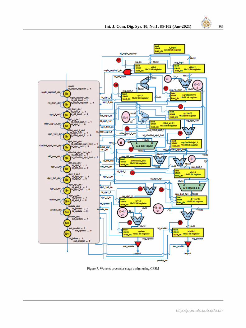
For proper coordination between the control unit and the datapath, synchronization is very important and this is achieved using clock signals. A good synchronization between the control unit and the datapath eliminates the negative effects of timing skew which causes unpredictability in output. Based on the atomic instructions and the atomic operations in Table 2, we propose the design of the wavelet processor stage as shown in Fig. 7 where the interconnection between the datapath and the control based on the atomic instructions and atomic operations of Table 2 can be seen.
6. HILBERT TRANSFORM PROCESSOR STAGE
DESIGN USING CFSM
Similar to the design of the wavelet stage of the
processor, the Hilbert transform stage is also designed
using CFSM, where the control unit is implemented
using FSM, and the datapath is implemented using RT-
level circuit. The complete design is shown in Fig. 8; the
design is such that the output from the wavelet processor
state is stored in a 16x32 bit RAM called hRAM. At each
rising edge of the clock, the contents of hRAM are
transferred one-by-one to a 1x32 bit register sequentially.
Thus when the control unit is in state S0, the first content
of hRAM is transferred to the first 1x32 bit register;
when the control unit transits to state S1, the content of
the first 1x32 register is transferred to the second 1x32 bit
register and so on.
The transfer in this order is possible because unlike
the load signal of a current state in the wavelet processor
stage which is turned OFF when the control unit makes a
transition to the next state, the load signal of the current
in the Hilbert transform control unit is not turned OFF
when there is a transition to the next state; this makes the
register load the next data into the register associated
with the previous state, while the current state loads the
previous data coming from the previous state.
By this mechanism, the Hilbert transform is able to
perform data transfer according to the structure shown in
Fig. 5b. As the data is transferred from one 1x32 bit
register to the next 1x32 bit register, the necessary
computations are performed by the floating point
subtractors, multipliers, and adders. When the Hilbert
transform stage of the processor completes the
computation, it triggers the ld_reg2n_2np1 signal in the
wavelet processor stage which begins another round of
computation for another data set.
7. DESIGN SIMULATION, VERIFICATION, AND
PERFORMANCE MEASUREMENT
In this section, the simulation of the design will be
performed, alongside verification of the design. This
section will also present the performance of the design
starting with the floating point multiplier,
adder/subtractor, the wavelet transform stage of the
processor, and then the Hilbert transform stage.
Table 6 shows the performance of the floating point
multiplier designed using Algorithm 1 where it can be
seen that the same level of performance was obtained
when compared with the Xilinx IPCORE. The root mean
squared error (RMSE) between the Xilinx IPCORE and
the proposed multiplier computed using the
relationship[34] 2
1ˆ(1 )
n
iRMSE n x x
was 0;
where n is the number of samples, x the value obtained
from Xilinx IPCORE, and x̂ the value from the proposed
multiplier. However, the proposed multiplier in this
paper was faster in the computation of the product of its
input at 650ns as shown in Fig. 9 than that of Xilinx
IPCORE at 850ns. Similarly, the floating point
adder/subtractor designed using Algorithm 2 gave the
same level of accuracy in comparison with the Xilinx
IPCORE with an RMSE = 0.000000xxx as shown in
Table 7. This value xxx of RMSE i.e. quantization error
caused by the difference in the internal representation of
floating point numbers between the proposed algorithm
and Xilinx IPCORE is insignificant to cause any
distortion in computation because it is highly accurate
and competes better than similar algorithms[34]–[37].
Fig. 10 shows that the proposed adder/subtractor gave the
same level of performance at a lesser time 450ns than the
Xilinx IPCORE adder/subtractor time of 1150ns.
Int. J. Com. Dig. Sys. 10, No.1, 85-102 (Jan-2021) 93
http://journals.uob.edu.bh
Figure 7. Wavelet processor stage design using CFSM

94 Peter Yusuf Dibal, et. al.: VLSI Design of a Processor for Discrete Wavelet Packet…
http://journals.uob.edu.bh
Figure 8. Hilbert processor stage design using CFSM
TABLE VI. COMPARISON BETWEEN PROPOSED FLOATING POINT MULTIPLIER AND XILINX IPCORE FLOATING POINT
MULTIPLIER
Operation Decimal Number IEEE-754 Floating Point Representation RMSE
Input 1
Input 2
1.2915000 00111111101001010100111111011111 9.3453000 01000001000101011000011001011001
sum - xilinx IP CORE adder 12.0694549 01000001010000010001110001111100 0.000000000
product - proposed adder 12.0694549 01000001010000010001110001111100
Input 1
Input 2
-2.3682000 11000000000101111001000010010111
6.4152000 01000000110011010100100101010010
sum - xilinx IP CORE adder -15.1924766 11000001011100110001010001100011 0.000000000
product - proposed adder -15.1924766 11000001011100110001010001100011

Int. J. Com. Dig. Sys. 10, No.1, 85-102 (Jan-2021) 95
http://journals.uob.edu.bh
TABLE VII. COMPARISON BETWEEN PROPOSED FLOATING POINT ADDER/SUBTRACTOR AND XILINX IPCORE FLOATING
POINT ADDER/SUBTRACTOR
Operation Decimal Number IEEE-754 Floating Point Representation RMSE
Input 1 1.2915000 00111111101001010100111111011111
Input 2
sum - xilinx IP CORE adder
9.3453000 01000001000101011000011001011001
10.6368000 01000001001010100011000001010101 0.000000999
sum - proposed adder 10.6367990 01000001001010100011000001010100
Input 1 -2.3682000 11000000000101111001000010010111
Input 2 6.4152000 01000000110011010100100101010010
difference - xilinx IP CORE
subtractor
4.0470000 01000000100000011000000100000110 0.000000400
difference - proposed subtractor 4.0470004 01000000100000011000000100000111
To test the performance of the wavelet stage of the
processor, the 32x32 bit register was populated with 32
data points each being 32bits wide. Simulation was
performed as shown in Fig. 11, where the wavelet stage
of the processor can be seen computing the first update
and predict values at the rising edge of the clock at
123250ns. The last or sixteenth values of the update and
predict values were computed at 124750ns. Fig. 12 shows
a zoomed-in view of some values computed by the
wavelet processor stage; the values shown are for the first
two and sixteenth values of both the update signal and
predict signal. To get to these results, the wavelet stage
performed all the computations in (6).
Table 8 shows the data points that were used in
testing the wavelet stage of the processor, alongside the
complete computed update and predict values. To further
validate the results obtained in Table 8, a model of the
wavelet processor stage was developed using Simulink as
shown in Fig. 13, and the results obtained confirm the
accuracy of the wavelet processor stage. The update
signal and the predict signal are fed concurrently into two
versions of the Hilbert transform that was designed
according to the architecture in Fig. 8. Simulation was
performed as shown in Fig. 14, where it can be that the
first Hilbert transform for the update and predict values
were computed at 311550ns, and the last Hilbert
transform for the update and predict values were
computed at 313050ns. A comparison between Fig. 11
and 14 shows that the Hilbert transform computations
started after the completion of the wavelet processor
stage computations. This is not unexpected based on the
architecture proposed in Fig. 7 and 8. The results
obtained from the simulation in Fig. 14 are shown in
Table 9, where the Hilbert transform of the update and
predict signals are presented. A zoomed-in view of some
of the results obtained in Fig. 14 is shown in Fig. 15 for
the first two values and the sixteenth value of the update
signal and predict signal respectively.
Figure 9. Floating point multiplier product computing time

96 Peter Yusuf Dibal, et. al.: VLSI Design of a Processor for Discrete Wavelet Packet…
http://journals.uob.edu.bh
Figure 10. Floating point adder/subtractor computing time
Figure 11. Computation of predict and update values by wavelet stage of processor
Figure 12. Zoomed-in view of first two and sixteenth wavelet transform values

Int. J. Com. Dig. Sys. 10, No.1, 85-102 (Jan-2021) 97
http://journals.uob.edu.bh
TABLE VIII. TEST DATA AND COMPUTED RESULTS FOR PROCESSOR WAVELET STAGE
S/N Input signal value
S/N IEEE-754 format Decimal IEEE-754 format Decimal
0 00111111000010011010011010110101 0.5377
Up
dat
e s
ign
al
0 00111111100101101000001111011011 1.175898 1 00111111111010101011110100111100 1.8339 1 10111110000001000001010010001111 -0.12898 2 11000000000100001001000000101110 -2.2588 2 10111111100010100110110100111011 -1.08145 3 00111111010111001011100100100100 0.8622 3 00111111000001010101011001000001 0.52084 4 00111110101000110011100111000001 0.3188 4 01000000010101100101111011010010 3.34953 5 10111111101001110110001010110111 -1.3077 5 01000000000000111010111010011001 2.05753 6 10111110110111100000000011010010 -0.4336 6 00111110111101111111001100000110 0.48427 7 00111110101011110110100101000100 0.3426 7 10111101010000000010011000111011 -0.04691 8 01000000011001010000010010000001 3.5784 8 00111111101010001100100010101110 1.31862 9 01000000001100010011110111011001 2.7694 9 01000000000010110000111010001000 2.17276 10 10111111101011001100100110000110 -1.3499 10 10111111001111000110100111011011 -0.73598 11 01000000010000100011101111001101 3.0349 11 00111111110101111100011000110110 1.68573 12 00111111001110011011001111010000 0.7254 12 00111111101001101110010001011111 1.30384 13 10111101100000010011101010010011 -0.0631 13 00111110100001111011000101010100 0.26502 14 00111111001101101111011010010100 0.7147 14 10111110001011010010000011011010 -0.16907 15 16
10111110010100011110101110000101 10111101111111100010100000100100
-0.2050 -0.1241
15 10111111000100011000111010100001 -0.56858
Pre
dic
t si
gnal
0 00111110110111110010111110011000 0.43591 17 00111111101111101010111001111101 1.4897 1 01000000001100100101011001001101 2.78651 18 00111111101101000101101000011101 1.4090 2 10111111011111110100111101101001 -0.99730 19 00111111101101010110011011001111 1.4172 3 00111110100011010111110101111101 0.27634 20 00111111001010111110011101101101 0.6715 4 10111111110100010100110010001100 -1.63514 21 10111111100110101000111101011100 -1.2075 5 01000000011010110110111110001100 3.67868 22 00111111001101111001101001101011 0.7172 6 10111110000001101110111100101111 -0.13177 23 00111111110100001010101001100101 1.6302 7 10111111000111011111110100000111 -0.61714 24 00111110111110100101000100011010 0.4889 8 00111111010111101010110100101001 0.86982 25 00111111100001000111000100001101 1.0347 9 10111110001101001001100001011101 -0.17636 26 00111111001110100001011000011110 0.7269 10 10111111001001010001110010000111 -0.64496 27 10111110100110110101011100111111 -0.3034 11 00111011011011111111100101011000 0.00366 28 00111110100101100111101000010000 0.2939 12 00111111000011001000011000111101 0.54892 29 10111111010010011000110001111110 -0.7873 13 10111110111010110011101100110011 -0.45943 30 00111111011000110110111000101111 0.8884 14 10111111000110011001101111101000 -0.60003 31 10111111100100101101010000101100 -1.1471 15 10111111101101111100000110001001 -1.43559
A verification model based on the Hilbert FIR
structure in Fig. 8 was developed and tested as shown in
Fig. 16. A comparison between the results shown in
Table 10 and Fig. 16 confirms the accuracy of the Hilbert
transform processor stage. A second comparison in the context of FPGA resource
utilization was also made between the design of the Hilbert transform processor presented in this paper and similar other designs; this is shown in Table 10 where it can be seen the Hilbert processor in this paper performs well in comparison with similar designs.
8. CONCLUSION
In this paper, we undertook the design of a processor
that computed the DWPT and then the Hilbert transform
of the DWPT of an input signal. The design approach
was based on the lifting steps of a Db4 wavelet for the
DWPT, and FIR technique for the Hilbert transform.
Using these approaches, an architecture was developed
for the processor datapath, after which the processor unit
was also developed. The arithmetic and logic unit (ALU)
of the datapath in Figs 7 and 8 were designed to perform
three basic primitive arithmetic operations:
multiplication, addition, and subtraction. These
operations are floating point in nature based on the IEEE-
754 single precision floating point arithmetic owing to
the fact that the data representation in the VLSI design of
the processor is also based on the IEEE-754 single
precision floating point format. Simulation results were
used to verify the performance of the processor, where
the DWPT of the input signal was computed based on the
lifting steps, and then the Hilbert transform of the DWPT
signal was subsequently computed in the second stage of
the processor. The waveform analysis of the results and
the tabulation of the simulation results confirmed that the
processor performed as expected.

98 Peter Yusuf Dibal, et. al.: VLSI Design of a Processor for Discrete Wavelet Packet…
http://journals.uob.edu.bh
Figure 13. Simulink verification model for wavelet processor stage
Figure 14. Computation of the Hilbert transform of update and predict values

Int. J. Com. Dig. Sys. 10, No.1, 85-102 (Jan-2021) 99
http://journals.uob.edu.bh
TABLE IX. HILBERT TRANSFORM OF UPDATE AND PREDICT SIGNALS
S/N IEEE-754 format Decimal IEEE-754 format Decimal
Up
dat
e s
ign
al
0 00111111100101101000001111011011 1.17589
Hilb
ert
tra
nsf
orm
10111111011110010010000111101101 -0.97317 1 10111110000001000001010010001111 -0.12898 00111101110110101001111010001100 0.10674 2 10111111100010100110110100111011 -1.08145 10111111001001110001111101000010 -0.65282 3 00111111000001010101011001000001 0.52084 10111110100001011100010101001000 -0.26127 4 01000000010101100101111011010010 3.34953 00111110010011000001000010101000 0.19928 5 01000000000000111010111010011001 2.05753 11000000001000111011100101010101 -2.55818 6 00111110111101111111001100000110 0.48427 11000000101010000101001100000001 -5.26013 7 10111101010000000010011000111011 -0.04691 11000000010001000001010111011111 -3.06383 8 00111111101010001100100010101110 1.31862 00111111111100100010110010000010 1.89198 9 01000000000010110000111010001000 2.17276 00111111010000000000100010111000 0.75013
10 10111111001111000110100111011011 -0.73598 01000000000000010110001011011100 2.02164 11 00111111110101111100011000110110 1.68573 11000000000110101000101110110000 -2.41476 12 00111111101001101110010001011111 1.30384 10111111000010000010111101011100 -0.53198 13 00111110100001111011000101010100 0.26502 11000000100111000001001000101110 -4.87720 14 10111110001011010010000011011010 -0.16907 11000000011000101101100010111111 -3.54446 15 10111111000100011000111010100001 -0.56858 01000000101111011001000111011011 5.92405
Pre
dic
t si
gnal
0 00111110110111110010111110011000 0.43591
Hilb
ert
tra
nsf
orm
10111110101110001011010101101010 -0.36075 1 01000000001100100101011001001101 2.78651 11000000000100111001011101111111 -2.30612 2 10111111011111110100111101101001 -0.99730 00111110100000001100111101010000 0.25158 3 00111110100011010111110101111101 0.27634 11000000011110010110000111011101 -3.89659 4 10111111110100010100110010001100 -1.63514 01000000010011110101100010111001 3.23979 5 01000000011010110110111110001100 3.67868 00111110100001001111000111011000 0.25965 6 10111110000001101110111100101111 -0.13177 00111111101001111001101010011110 1.30940 7 10111111000111011111110100000111 -0.61714 11000000000000010110111011000010 -2.02238 8 00111111010111101010110100101001 0.86982 11000000101110101001000101110111 -5.83025 9 10111110001101001001100001011101 -0.17636 01000000110010001111110010100010 6.28083
10 10111111001001010001110010000111 -0.64496 11000000110000010001101001110110 -6.03448 11 00111011011011111111100101011000 0.00366 01000000101101100110111011101010 5.70103 12 00111111000011001000011000111101 0.54892 00111111110110000101100111010100 1.69024 13 10111110111010110011101100110011 -0.45943 00111111011100010010000111011100 0.94192 14 10111111000110011001101111101000 -0.60003 11000000000000010001000101010100 -2.01668 15 10111111101101111100000110001001 -1.43559 10111111111011111010101101111011 -1.87242
Figure 15. Zoomed-in view of first two and sixteenth values of Hilbert transform
TABLE X. PERFORMANCE COMPARISON OF PROPOSED HILBERT TRANSFORM PROCESSOR WITH SIMILAR PROCESSORS
Title of work LUTs FF IoBs BRAM Mults DSP GCLK BUF
G FPGA-Based implementation of instantaneous frequency estimation of
phonocardiographic signals [38]
5,555 2,168 49 2 4 - 1 - Embedded Hilbert transform based algorithm within an FPGA to classify
nonlinear SDOG systems [39]
8,511 7,078 - 26 20 - - -
Efficient Architecture For Real Time Implementation of Hilbert Transform in
FPGA [34]
3,525 2,168 49 - - - - -
A High Performance Pipelined Discrete Hilbert Transform Processor [40] 6,486 5,268 - - - - - -
Ultrasound B-Mode Back End Signal Processor on FPGA [41]
2,190 883 52 134 - 21 - 1
Proposed Hilbert Transform processor 2,597 4,536 34 - - 2 - 1

100 Peter Yusuf Dibal, et. al.: VLSI Design of a Processor for Discrete Wavelet Packet…
http://journals.uob.edu.bh
Figure 16. Simulink-State flow verification model for Hilbert transform
REFERENCES
[1] P. Y. Dibal, E. N. Onwuka, J. Agajo, and C. Alenoghena,
“Enhanced Discrete Wavelet Packet Sub-band Frequency Edge
Detection using Hilbert Transform,” Int. J. Wavelets, Multiresolution Inf. Process., vol. 16, no. 1, pp. 1850009-1-
1850009–17, 2018.
[2] H. Wang and X. Chen, “Development and Optimization Design of Digital Logic device based on FPGA,” J. Phys. Conf. Ser., vol.
1345, no. 062051, pp. 1–9, 2019.
[3] J. Ashenden, P, Digital Design: An Embedded Systems Approach using VHDL. Burlington: Morgan Kaufmann.
[4] P. Chu, P, FPGA Prototyping by VHDL Examples. New Jersey:
John Wiley & Sons, 2008.
[5] M. Ravi, A. Sewa, S. T.G., and S. S. S. Sanagapati, “FPGA as a
Hardware Accelerator for Computation Intensive Maximum
Likelihood Expectation Maximization Medical Image Reconstruction Algorithm,” IEEE Access, vol. 7, pp. 111727–
111735, 2019.
[6] R. Krishnamoorthy, P. T. Kalaivaani, and A. S. Reddy, “An
Advanced Multiplier less Prediction Scheme based on Discrete
Wavelet Transformation Approach for Image Analysis,” Int. J. Recent Technol. Eng., vol. 7, no. 4S, pp. 511–518, 2018.
[7] H. I. Shahadi, R. Jidin, and H. Way, W, “High Performance
FPGA Architecture for Dual Mode Processor of Integer Haar Lifting-Based Wavelet Transform,” Int. Rev. Comput. Softw., vol.
8, no. 9, pp. 2058–2067, 2013.
[8] M. A. FARAHANI and M. ESHGHI, “Implementing a New Architecture of Wavelet Packet Transform on FPGA,” in 8th
WSEAS International Conference on Acoustics & Music: Theory
& Applications, 2007, pp. 37–41.
[9] Y. Liu and E. K. Lai, “Design and Implementation of An RNS-
Based 2-D DWT Processor,” IEEE Trans. Consum. Electron., vol.
50, no. 1, pp. 376–386, 2004.
[10] W. Xu, Z. YAN, and D. SHUNYING, “A High Performance
Pipelined Discrete Hilbert Transform Processor,” WSEAS Trans.
Signal Process., vol. 1, no. 9, pp. 21–30, 2013.
[11] A. A. Assef, B. M. Ferreira, J. M. Maia, and E. T. Costa,
“Modeling and FPGA-based implementation of an efficient and
simple envelope detector using a Hilbert Transform FIR filter for ultrasound imaging applications,” Reasearch Biomed. Eng., vol.
34, no. 1, pp. 87–92, 2018.
[12] H. Nikookar, Wavelet Radio: Adaptive and Reconfigurable Wireless Systems Based on Wavelets. Cambridge: Cambridge
University Press, 2013.
[13] Y. Arjoune and N. Kaabouch, “A Comprehensive Survey on Spectrum Sensing inCognitive Radio Networks: Recent
Advances,New Challenges, and Future Research Directions,”
MDPI Sensors, vol. 19, no. 126, pp. 1–32, 2019.
[14] Q. Zhinjin, N. Wang, G. Yue, and C. Laurie, “Adaptive Threshold
for Energy Detector Based on Discrete Wavelet Packet
Transform,” in Wireless Telecommunications Symposium, 2012, pp. 1–5.
[15] N. Wei, Z. Chen, and A. Zhu, “Research on Adaptive Resolution
Spectrum Sensing Method Based on Discrete Wavelet Packet Transform,” Telkomnika Indones. J. Electr. Eng., vol. 12, no. 2,
pp. 1385 – 1394, 2014.
[16] I. Daubechies and W. Sweldens, “Factoring Wavelet Transforms into Lifting Steps,” J. Fourier Anal. App.l, vol. 4, pp. 247 – 269,
1998.
[17] W. Lewis, D, Fundamentals of Embedded Software: Where C and Assembly meet. New Jersey: Prentice Hall, 2002.

Int. J. Com. Dig. Sys. 10, No.1, 85-102 (Jan-2021) 101
http://journals.uob.edu.bh
[18] K. Mishra, S, V. Nandanwar, A. Ayele, E, and B. Dhok, S, “FPGA Implementation of Single Precision Floating Point
Multiplier using High Speed Compressors,” Int. J. Soft Comput.
Eng., vol. 14, no. 2, pp. 18–23, 2014.
[19] R. Fay, A. Hsieh, D. Jeang, and B. Jenkins, “A Synthesizable
VHDL Floating Point Package.” John Hopkins University ECE
Department, 2011.
[20] U. Concordia, “Concordia, University Lectures,” 2010. [Online].
Available:
http://users.encs.concordia.ca/~asim/COEN_6501/Lecture_Notes/L4_Slides.pdf. [Accessed: 11-Jun-2018].
[21] Z. Peng, P. Tse, and F. Chu, “A comparison study of improved
Hilbert-Huang transform and wavelet transform: Application to fault diagnosis for rolling bearing,” Mech. Syst. Signal Process,
vol. 19, pp. 974 – 988, 2005.
[22] N. Saravanan, “Gear box Fault Diagnosis using Hilbert Transform Feature Classification by PVSM,” Int. J. Adv. Res. Comput. Sci.
Softw. Eng., vol. 6, no. 6, pp. 21 – 30, 2016.
[23] A. Fedotov, A. Akulova, and S. Akulov, “Effective QRS-Detector Based on Hilbert Transform and Adaptive Thresholding,” in XIV
Mediterranean Conference on Medical and Biological
Engineering and Computing, 2016, pp. 140 – 144.
[24] S. Aditi, “Survey Paper on Hilbert Transform with its Application
in Signal Processing,” Int. J. Comput. Sci. Inf. Technol., vol. 5, no.
3, pp. 3880 – 3882, 2014.
[25] E. Romero, D, G. Jimenez, M, and G. Dolecek, J, “On the
Estimation of Minimum Number of Distinct Multipliers in FIR
Hilbert Transformers Based on Frequency Transformation,” in The 2013 Iberoamerican Conference on Electronics Engineering
and Computer Science, 2013, pp. 88–95.
[26] G. Lyons, R, Understanding Digital Signal Processing, 2nd ed. New Jersey: Prentice Hall, 2004.
[27] S. Diniz, P, A. Silva, E, and L. Netto, S, Digital Signal
Processing: System Analysis and Design, 2nd ed. New York: Cambridge University Press, 2010.
[28] J. Orfanidis, S, Introduction to Signal Processing. New York:
Prentice Hall, 2010.
[29] K. Ingle, V and G. Proakis, J, Digital Signal Processing using
MATLAB, 3rd ed. Stamford CT: Cengage Learning, 2010.
[30] F. Harris, J, “On the Use of Windows for Harmonic Analysis with
Discrete Fourier Transform,” Proc. IEEE, no. 1, pp. 51–83, 1978.
[31] S. Chakraborty, “Advantages of Blackman Window over
Hamming Window Method for Design of FIR Filter,” Int. J.
Comput. Sci. Eng. Technol., vol. 4, no. 8, pp. 1181–1189, 2013.
[32] Xilinx, “Xilinx FIR Compiler v7.2,” 2020. [Online]. Available: https:www.xilinx.com/support/documentation/ip_documentation/f
ir_compiler/v7_2/pg149-fir-compiler.pdf. [Accessed: 17-May-
2020].
[33] A. Benso, “Introduction to Complex FSMs Design.” Torino, pp.
1–38, 2011.
[34] A. A. Prince, P. K. Verma, C. Jayakumar, and D. Raju, “Efficient Architecture For Real Time Implementation of Hilbert Transform
in FPGA,” in Electrical, Computer and Communication
Technologies (ICECCT), 2015 IEEE International Conference on. IEEE, 2015, pp. 1–5.
[35] M. D. Linderman, M. Ho, D. L. Dill, T. H. Meng, and G. P. Nolan, “Towards Program Optimization through Automated
Analysis of Numerical Precision,” in Proc CGO, 2010, pp. 230–
237.
[36] T. Aamodt and P. Chow, “Numerical error minimizing floating-
point to fixed-point ANSI C compilation,” in 1st Workshop on
Media Processors and DSPs, 1999, pp. 3–12.
[37] N. Wiebe and V. Kliuchnikov, “Floating point representations in
quantum circuit synthesis,” New J. Phys., vol. 15, no. 093041, pp.
1–25, 2013.
[38] E. Hernandez, J. Toledo, J. Martinez, and R. Ruiz, “FPGAbased
implementation of the instantaneous frequency estimation of
phonocardiographic signals,” in International Federation of Auto. Control workshop on Programmable Devices and Systems, 2004,
pp. 423–428.
[39] J. D. Jones, J. S. Pei, and M. P. Tull, “Embedded Hilbert transform based algorithm within an FPGA to classify nonlinear
SDOG systems,” in Proceedings of the23rd International Modal
Analysis Conference, 2008.
[40] W. Xu, Z. Yan, and D. Shunying, “A High Performance Pipelined
Discrete Hilbert Transform Processor,” WSEAS Trans. SIGNAL
Process., vol. 9, no. 1, pp. 1–6, 2013.
[41] U. k Jayaraj, S. Gayathri, and A. Shamya, “Ultrasound B-Mode
Back End Signal Processor on FPGA,” Int. J. Eng. Res. Technol.,
vol. 4, no. 6, pp. 583–588, 2015.
Peter Yusuf Dibal has a PhD
student in communication at the
Federal University of Technology
Minna. He holds a Master’s
degree in Electronics and
Communications Engineering
from Teesside University in the
UK. His research interests are
digital signal processing,
communications, and VLSI
design.
Elizabeth N. Onwuka is a
Professor of
Telecommunications
Engineering. She holds a PhD in
Communications and
Information Systems
Engineering, from Tsinghua
University, Beijing, People’s
Republic of China; a Master of
Engineering degree, in
Telecommunications; and a Bachelor of Engineering degree
from Electrical and Computer Engineering Department, Federal
University of Technology (FUT) Minna, Niger State, Nigeria.
Her research interest includes Mobile communications network,
Mobile IP networks, Handoff management, Paging, Network
integration, Resource management in wireless networks,
spectrum management, and Big Data Analytics.

102 Peter Yusuf Dibal, et. al.: VLSI Design of a Processor for Discrete Wavelet Packet…
http://journals.uob.edu.bh
James Agajo has a PhD in the field
of Telecommunication and
Computer, Signal Processing. He
also has a Master’s Degree in
Electronic and Telecommunication
Engineering. His research interest
is in Wireless Sensor Systems,
and Network and intelligent
system development.
Caroline O. Alenoghena holds a
PhD in Telecommunications
Engineering, and a Master’s degree
in Electronics
Telecommunications. She is a
member of the Institute of
Electrical and Electronic Engineers
MIEEE, Nigerian Society of
Engineers (NSE), and Association
of Professional Women Engineers
of Nigeria APWEN. She is a
registered practicing Engineer with
the Council for the Regulation of
Engineering in Nigeria. Her research interests include
intelligent systems and networks.
Achonu Adejo obtained a first
degree in Electrical/Computer
Engineering from Federal
University of Technology Minna,
Nigeria in 2006, an MSc in
Electronic Communications and
Computer Engineering from
University of Nottingham (Malaysia
campus) in 2010 and a PhD in
Electrical Engineering from
Newcastle University, UK in 2018. His doctorate program was
carried out in the Communications, Sensors and Signal
processing group at School of Engineering. Since 2010, he has
been an academic staff with Federal University of Technology
Minna. His research interests and previous works are in
Minimal computer processors, FPGAs, Resource management
and modelling of Cellular communications with focus on 5G
communications and D2D networks.