Vivado Design Suite Tutorial - Xilinx · this tutorial has its own folder within the zip file. To...
148
Vivado Design Suite Tutorial Partial Reconfiguration UG947 (v2019.1) June 12, 2019
Transcript of Vivado Design Suite Tutorial - Xilinx · this tutorial has its own folder within the zip file. To...
Vivado Design Suite
Tutorial
Partial Reconfiguration
UG947 (v2019.1) June 12, 2019

Partial Reconfiguration www.xilinx.com 2 UG947 (v2019.1) June 12, 2019
Revision History The following table shows the revision history for this document.
Section Revision Summary
06/12/2019 Version 2019.1
General updates Validated for 2019.1 release.
Updated various links.
Lab 6: Partial Reconfiguration Controller IP for
UltraScale Devices
Corrected references to new lab.
12/20/2018 Version 2018.3
Lab 7: Partial Reconfiguration Controller IP for
UltraScale+ Devices
Added new lab.
04/27/2018 Version 2018.1
General updates Validated for 2018.1 release.
Updated menu commands.
Lab 1: 7 Series Basic Partial Reconfiguration Flow Rewrote lab to work with updated design files.
Overview New section in Lab 1.
Step 4: Assembling and Implementing the Design Added a step for setting board and part variables.
Lab 2: UltraScale Basic Partial Reconfiguration Flow Rewrote lab to work with updated design files.
Overview New section in Lab 2.
Step 4: Assembling and Implementing the Design Added a step for setting board and part variables.
Run the PR Configuration Analysis Report Added information on including submodule IP in the
PR Configuration Analysis Report.
Send Feedback

Partial Reconfiguration www.xilinx.com 3 UG947 (v2019.1) June 12, 2019
Table of Contents
Revision History ........................................................................................................................................................... 2
Introduction 6
Overview ........................................................................................................................................................................ 6
Hardware and Software Requirements .............................................................................................................. 7
Tutorial Design Description .................................................................................................................................... 7
Lab 1: 7 Series Basic Partial Reconfiguration Flow ........................................................................................... 10
Overview ...................................................................................................................................................................... 10
Step 1: Extracting the Tutorial Design Files .................................................................................................... 10
Step 2: Examining the Scripts ............................................................................................................................... 10
Step 3: Synthesizing the Design .......................................................................................................................... 12
Step 4: Assembling and Implementing the Design ..................................................................................... 12
Step 5: Building the Design Floorplan .............................................................................................................. 14
Step 6: Implementing the First Configuration ............................................................................................... 20
Step 7: Implementing the Second Configuration ......................................................................................... 25
Step 8: Examining the Results with Highlighting Scripts ........................................................................... 27
Step 9: Generating Bitstreams ............................................................................................................................. 28
Step 10: Partially Reconfiguring the FPGA ...................................................................................................... 30
Conclusion ................................................................................................................................................................... 32
Lab 2: UltraScale Basic Partial Reconfiguration Flow ....................................................................................... 33
Overview ...................................................................................................................................................................... 33
Step 1: Extracting the Tutorial Design Files .................................................................................................... 33
Step 2: Examining the Scripts ............................................................................................................................... 33
Step 3: Synthesizing the Design .......................................................................................................................... 35
Step 4: Assembling and Implementing the Design ..................................................................................... 35
Step 5: Building the Design Floorplan .............................................................................................................. 37
Step 6: Implementing the First Configuration ............................................................................................... 40
Step 7: Implementing the Second Configuration ......................................................................................... 45
Step 8: Examining the Results with Highlighting Scripts ........................................................................... 47
Send Feedback
Introduction
Partial Reconfiguration www.xilinx.com 4 UG947 (v2019.1) June 12, 2019
Step 9: Generating the Bitstreams ..................................................................................................................... 49
Step 10: Partially Reconfiguring the FPGA ...................................................................................................... 52
Conclusion ................................................................................................................................................................... 53
Lab 3: Partial Reconfiguration Project Flow ........................................................................................................ 54
Overview ...................................................................................................................................................................... 54
Step 1: Extracting the Tutorial Design Files .................................................................................................... 54
Step 2: Loading Initial Design Sources ............................................................................................................. 54
Step 3: Completing the Design with the Partial Reconfiguration Wizard ........................................... 58
Step 4: Synthesizing and Implementing the Current Design ................................................................... 62
Step 5: Adding an Additional Reconfigurable Module and Corresponding Configuration ......... 66
Step 6: Creating and Implementing a Greybox Module ............................................................................ 68
Step 6: Modifying a Design Source or Options ............................................................................................. 71
Conclusion ................................................................................................................................................................... 72
Lab 4: Vivado Debug and the PR Project Flow .................................................................................................. 73
Overview ...................................................................................................................................................................... 73
Step 1: Loading Initial Design Sources ............................................................................................................. 73
Step 2: Setting Up the Design for Partial Reconfiguration ....................................................................... 76
Step 3: Using the Partial Reconfiguration Wizard to Complete the Rest of the Design ............... 78
Step 4: Adding IP within the Reconfigurable Module ................................................................................ 82
Step 5: Synthesizing the Design and Creating a Floorplan ...................................................................... 84
Step 6: Running the PR Configuration Analysis Report ............................................................................. 88
Step 7: Implementing the Design ....................................................................................................................... 89
Step 8: Adding an Additional Reconfigurable Module and Corresponding Configuration ......... 93
Step 9: Generating Bitstreams ............................................................................................................................. 97
Step 10: Connecting to the Board and Programming the FPGA ............................................................ 97
Conclusion ................................................................................................................................................................ 104
Lab 5: Partial Reconfiguration Controller IP for 7 Series Devices ............................................................ 105
Step 1: Extracting the Tutorial Design Files ................................................................................................. 105
Step 2: Customizing the Partial Reconfiguration Controller IP ............................................................ 105
Step 3: Compiling the Design ........................................................................................................................... 112
Step 4: Setting up the Board ............................................................................................................................. 113
Send Feedback
Introduction
Partial Reconfiguration www.xilinx.com 5 UG947 (v2019.1) June 12, 2019
Step 5: Operating the Sample Design ........................................................................................................... 114
Step 6: Querying the PRC in the FPGA .......................................................................................................... 116
Step 7: Modifying the PRC in the FPGA ........................................................................................................ 118
Conclusion ................................................................................................................................................................ 120
Lab 6: Partial Reconfiguration Controller IP for UltraScale Devices ........................................................ 121
Step 1: Extracting the Tutorial Design Files ................................................................................................. 121
Step 2: Customizing the Partial Reconfiguration Controller IP ............................................................ 121
Step 3: Compiling the Design ........................................................................................................................... 128
Step 4: Setting up the Board ............................................................................................................................. 129
Step 5: Operating the Sample Design ........................................................................................................... 129
Step 6: Querying the PRC in the FPGA .......................................................................................................... 130
Step 7: Modifying the PRC in the FPGA ........................................................................................................ 132
Conclusion ................................................................................................................................................................ 134
Lab 7: Partial Reconfiguration Controller IP for UltraScale+ Devices ..................................................... 135
Overview ................................................................................................................................................................... 135
Step 1: Extracting the Tutorial Design Files ................................................................................................. 135
Step 2: Processing the Tutorial Design .......................................................................................................... 135
Step 3: Running the Tutorial Design .............................................................................................................. 140
Conclusion ................................................................................................................................................................ 147
Legal Notices 148
Please Read: Important Legal Notices ........................................................................................................... 148
Send Feedback
Partial Reconfiguration www.xilinx.com 6 UG947 (v2019.1) June 12, 2019
Introduction
Overview This tutorial covers the Partial Reconfiguration (PR) software support in Vivado® Design Suite
release 2018.3.
Lab 1: 7 Series Basic Partial Reconfiguration Flow and Lab 2: UltraScale Basic Partial
Reconfiguration Flow step through basic information about the current Partial Reconfiguration
(PR) design flow, example Tcl scripts, and show results within the Vivado integrated design
environment (IDE). You run scripts for part of the lab and work interactively with the design for
other parts. You can also script the entire flow, and a completed script is included with the
design files. These labs focus specifically on the software flow from RTL to bitstream,
demonstrating how to process a Partial Reconfiguration design. Lab 2 also applies to
UltraScale+™ devices.
Lab 3: Partial Reconfiguration Project Flow steps you through the project flow within the Vivado
IDE, from establishing the design using the Partial Reconfiguration Wizard to synthesis, iteration
runs, and then iterating the design. Lab 4: Vivado Debug and the PR Project Flow also walks you
through the project flow, but includes adding IP, debug cores, and debugging through the
Vivado Hardware Manager.
Lab 5: Partial Reconfiguration Controller IP for 7 Series Devices, Lab 6: Partial Reconfiguration
Controller IP for UltraScale Devices, and Lab 7: Partial Reconfiguration Controller IP for
UltraScale+ Devices are designed to show the fundamental details and capabilities of the Partial
Reconfiguration Controller (PRC) IP in the Vivado Design Suite. Managing partial bitstreams is
one of the new design requirements introduced by PR: designers plan for when partial
bitstreams are required, where they are stored, how they are delivered to the configuration
engine, and how the static design behaves before, during and after the delivery of a new partial
bitstream. The PRC IP is designed to help users solve these challenges.
Additional Resources
For additional information, see the following documents:
• Vivado Design Suite User Guide: Partial Reconfiguration (UG909)
• Partial Reconfiguration Controller Product Guide (PG193)
• DocNav includes a Partial Reconfiguration Design Hub that links these documents and
other PR-specific resources. It is also available through the Xilinx support site.
Send Feedback

Introduction
Partial Reconfiguration www.xilinx.com 7 UG947 (v2019.1) June 12, 2019
VIDEO:
The following videos provide an overview of Vivado Partial Reconfiguration solutions:
• Vivado Design Suite QuickTake Video Tutorial: Partial Reconfiguration in Vivado
• Vivado Design Suite QuickTake Video Tutorial: Partial Reconfiguration for
UltraScale
• Vivado Design Suite QuickTake Video Tutorial: Partial Reconfiguration for
UltraScale+
• Vivado Design Suite QuickTake Video Tutorials
TRAINING: Xilinx provides training courses that can help you learn more about the
concepts presented in this document. Use the link to explore related courses:
• Xilinx Partial Reconfiguration Tools & Techniques
• Partial Reconfiguration Flow on Zynq using Vivado
Hardware and Software Requirements This tutorial requires that the 2018.3 Vivado Design Suite software release or later is installed. A
Partial Reconfiguration license is required to run the PR software tools in the Vivado Design
Suite. If necessary, request access by sending an email to [email protected] for a 30-day
evaluation license. A valid corporate or university email address is required.
The labs in this tutorial document target eight different Xilinx development platforms. Unless
specifically noted, production silicon and production boards are required to match the
instructions in each lab. For Operating Systems support, see the Vivado Design Suite User
Guide: Release Notes, Installation, and Licensing (UG973) for a complete list and description of
the system and software requirements.
Tutorial Design Description Designs for the tutorial labs are available as a zipped archive on the Xilinx website. Each lab in
this tutorial has its own folder within the zip file. To access the tutorial design files:
1. Download the Reference Design Files from the Xilinx website.
2. Extract the zip file contents to any write-accessible location.
Lab 1: 7 Series Basic Partial Reconfiguration Flow
The sample design used throughout this tutorial is called led_shift_count_7s. The design
targets the following Xilinx development platforms:
• KC705 (xc7k325t)
• VC707 (xc7vx485t)
Send Feedback

Introduction
Partial Reconfiguration www.xilinx.com 8 UG947 (v2019.1) June 12, 2019
• VC709 (xc7vx690t)
• AC701 (xc7a200t)
This design is very small, which helps minimize data size and allows you to run the tutorial
quickly, with minimal hardware requirements.
Lab 2: UltraScale Basic Partial Reconfiguration Flow
The sample design used throughout this tutorial is called led_shift_count_us. The design
targets the following Xilinx development platforms:
• KCU105 (xcku040)
• VCU108 (xcvu095)
• KCU116 (xcku5p)
• VCU118 (xcvu9p)
Lab 3 Partial Reconfiguration Project Flow
The sample design used throughout this tutorial is called pr_project. It is a modified version
of the led_shift_count design used in Lab 1, modified to include two shift instances instead
of one counter and one shifter. This change helps illustrate that a Partition Definition applies to
all instances of a partition type. The design targets the following Xilinx development platforms:
• KC705 (xc7k325t)
• VC707 (xc7vx485t)
• VC709 (xc7vx690t)
• KCU105 (xcku040)
• KCU116 (xcku5p)
• VCU108 (xcvu095)
• VCU118 (xcvu9p)
Lab 4: Vivado Debug and the PR Project Flow
The sample design used is called pr_project_debug. The design targets the following Xilinx
development platforms:
• KCU105 (xcku040)
• VCU108 (xcvu095)
• KCU116 (xcku5p)
• VCU118 (xcvu9p)
Send Feedback

Introduction
Partial Reconfiguration www.xilinx.com 9 UG947 (v2019.1) June 12, 2019
Lab 5: Partial Reconfiguration Controller IP for 7 Series Devices
The sample design used throughout this tutorial is called prc_7s and is based on the design
used in Lab 1. The design targets the following Xilinx development platforms:
• KC705 (xc7k325t)
• VC707 (xc7vx485t)
• VC709 (xc7vx690t)
Lab 6: Partial Reconfiguration Controller IP for UltraScale Devices
The sample design used throughout this tutorial is called prc_us. The design targets an
xcvu095 device for use on the VCU108 demonstration board, Rev 1.0, and is based on the
design used in Lab 2.
Lab 7: Partial Reconfiguration Controller IP Tutorial Design
The sample design used throughout this tutorial is called prc_usp and is based on the design
used in Lab 6. The design targets the KCU116 and VCU118 demonstration boards.
Send Feedback

Partial Reconfiguration www.xilinx.com 10 UG947 (v2019.1) June 12, 2019
Lab 1: 7 Series Basic Partial Reconfiguration Flow
Overview This lab introduces the basic PR flow for 7 series devices. First, you will use a script to
individually synthesize the static module and each reconfigurable design module variant. Then
in the IDE, you will constrain the location of the reconfigurable modules (RM) using Pblocks and
implement the initial configuration of the design. Next, you will implement alternate
configurations by locking the static portion of the design, updating the reconfigurable modules
with a variant, and re-running implementation. Finally, you will verify that each implemented RM
is compatible with the static portion of the design and, if compatible, generate bitstreams.
Step 1: Extracting the Tutorial Design Files 1. To obtain the tutorial design file, see Tutorial Design Description.
2. Navigate to \led_shift_count_7s in the extracted files. The led_shift_count_7s
data directory is referred to in this lab as the <Extract_Dir>.
Step 2: Examining the Scripts Start by reviewing the scripts provided in the design archive. The files run_pr.tcl and
advanced_settings.tcl are located at the root level. The run_pr.tcl script contains the
minimum required settings to run partial reconfiguration. The advanced_settings.tcl
contains default flow settings and should only be modified by experienced users.
The Main Script
In the <Extract_Dir>, open run_pr.tcl in a text editor. This is the master script where you
define the design parameters, design sources, and design structure. This is the only file you have
to modify to compile a complete Partial Reconfiguration design. Find more details regarding
run_pr.tcl, advanced_settings.tcl, and the underlying scripts in the README.txt
located in the Tcl_HD subdirectory.
Note the following details in run_pr.tcl:
• Under Define target demo board, you can select one of many demonstration boards
supported for this design.
• Under flow control, you can control what phases of synthesis and implementation are
run. In the tutorial, only synthesis is run by the script; implementation, verification, and
Send Feedback
Lab 1: 7 Series Basic Partial Reconfiguration Flow
Partial Reconfiguration www.xilinx.com 11 UG947 (v2019.1) June 12, 2019
bitstream generation are run interactively. To run these additional steps via the script, set
the flow variables (e.g., run.prImpl) to 1.
• The Output Directories and Input Directories set the file structure expected for design
sources and results files. You must reflect any changes to your file structure here.
• The Top Definition and RP Module Definitions sections allow you to reference all
source files for each part of your design. Top Definition covers all sources needed for the
static design, including constraints and IP. The RP Module Definitions section does the
same for Reconfigurable Partitions (RP). Identify each RP and list all Reconfigurable
Module (RM) variants for each RP.
o This design has two Reconfigurable Partitions (inst_shift and inst_count), and
each RP has two module variants.
• The Configuration Definition sections define the sets of static and reconfigurable
modules that make up a configuration.
o This design has two configurations,
Config_shift_right_count_up_implement and
Config_shift_left_count_down_import. You can create more configurations
by adding RMs or by combining existing RMs.
The Supporting Scripts
Underneath the Tcl_HD subdirectory, several supporting Tcl scripts exist. The scripts are called
by run_pr.tcl, and they manage specific details for the Partial Reconfiguration flow. Provided
below are some details about a few of the key PR scripts.
CAUTION! Do not modify the supporting Tcl scripts.
• step.tcl
Manages the current status of the design by monitoring checkpoints.
• synthesize.tcl
Manages the details regarding the synthesis phase.
• implement.tcl
Manages the details regarding the module implementation phase.
• pr_utils.tcl
Manages the details regarding the top-level implementation of a PR design.
• run.tcl
Launches the actual runs for synthesis and implementation.
• log_utils.tcl
Handles report file creation at key points during the flow.
Send Feedback

Lab 1: 7 Series Basic Partial Reconfiguration Flow
Partial Reconfiguration www.xilinx.com 12 UG947 (v2019.1) June 12, 2019
Remaining scripts provide details within these scripts (such as other *_utils.tcl scripts) or
manage other Hierarchical Design flows (such as hd_utils.tcl).
Step 3: Synthesizing the Design The run_pr.tcl script automates the synthesis phase of this tutorial. Five iterations of
synthesis are called, one for the static top-level design and one for each of four Reconfigurable
Modules.
3. Open the Vivado Tcl shell:
• On Windows, select the Xilinx Vivado desktop icon or Start > All Programs > Xilinx
Design Tools> Vivado 2018.x > Vivado 2018.x Tcl Shell.
• On Linux, simply type, vivado -mode tcl.
4. In the shell, navigate to the <Extract_Dir> directory.
5. If you are using a target demonstration board other than the KC705, modify the xboard
variable in run_pr.tcl. Valid alternatives are the VC707, VC709 and AC701 boards.
6. Run the run_pr.tcl script by entering:
source run_pr.tcl -notrace
After all five passes through Vivado Synthesis have completed, the Vivado Tcl shell remains
open. You can find log and report files for each module, alongside the final checkpoints, under
each named folder in the Synth subdirectory.
TIP: In the <Extract_Dir> directory, multiple log files have been created:
• run.log shows the summary as posted in the Tcl shell window
• command.log echoes all the individual steps run by the script
• critical.log reports all critical warnings produced during the run
Step 4: Assembling and Implementing the Design Now that the synthesized checkpoints for each module, plus top, are available, you can
assemble the design.
You will run all flow steps from the Tcl Console, but you can use features within the IDE (such as
the floorplanning tool) for interactive events.
TIP: Copy and paste commands directly from the tutorial to avoid redundant effort
and typos in the Vivado IDE. Copy and paste only one full command at a time. Note
that some commands are long and span multiple lines.
Send Feedback

Lab 1: 7 Series Basic Partial Reconfiguration Flow
Partial Reconfiguration www.xilinx.com 13 UG947 (v2019.1) June 12, 2019
1. Open the Vivado IDE. You can open the IDE from the open Tcl shell by typing start_gui or
by launching Vivado with the command vivado -mode gui.
2. Navigate to the <Extract_Dir> directory if you are not already there. The pwd command
can confirm this.
3. Set variables that help with copying commands from this document into the Tcl Console.
Select the part and board you are targeting for this lab, and apply them in Vivado:
set part "xc7k325t-ffg900-2"
set board "kc705"
set part "xc7vx485t-ffg1761-2"
set board "vc707"
set part "xc7vx690t-ffg1761-2"
set board "vc709"
set part "xc7a200t-fbg676-2"
set board "ac701"
4. Create an in-memory design by issuing the following command in the Tcl Console:
create_project -in_memory -part $part
5. Load the static design by issuing the following command:
add_files ./Synth/Static/top_synth.dcp
6. Load the top-level design constraints by issuing these commands:
add_files ./Sources/xdc/top_io_$board.xdc
set_property USED_IN {implementation} [get_files ./Sources/xdc/top_io_$board.xdc]
Selecting the top_io_$board version of the available xdc file loads the pin location and
clocking constraints, but does not include floorplan information. The top_$board version
includes pin location, clocking and floorplanning constraints.
7. Load the first two synthesis checkpoints for the shift and count functions by issuing these
commands:
add_files ./Synth/shift_right/shift_synth.dcp
set_property SCOPED_TO_CELLS {inst_shift} [get_files ./Synth/shift_right/shift_synth.dcp]
add_files ./Synth/count_up/count_synth.dcp
set_property SCOPED_TO_CELLS {inst_count} [get_files ./Synth/count_up/count_synth.dcp]
The SCOPED_TO_CELLS property ensures that the proper assignment is made to the target
cell. See this link in Vivado Design Suite User Guide: Using Constraints (UG903) for more
information.
8. Link the entire design together using the link_design command:
link_design -mode default -reconfig_partitions {inst_shift inst_count} -part $part -top top
Send Feedback
Lab 1: 7 Series Basic Partial Reconfiguration Flow
Partial Reconfiguration www.xilinx.com 14 UG947 (v2019.1) June 12, 2019
At this point a full configuration is loaded, including static and reconfigurable logic. Note
that the Flow Navigator pane is not present while you are working in non-project mode.
TIP: Place the IDE in floorplanning mode by selecting Layout > Floorplanning. Make
sure the Device view is visible.
9. Save the assembled design state for this initial configuration:
write_checkpoint -force ./Checkpoint/top_link_right_up.dcp
Step 5: Building the Design Floorplan Next, create a floorplan to define the regions that will be partially reconfigured.
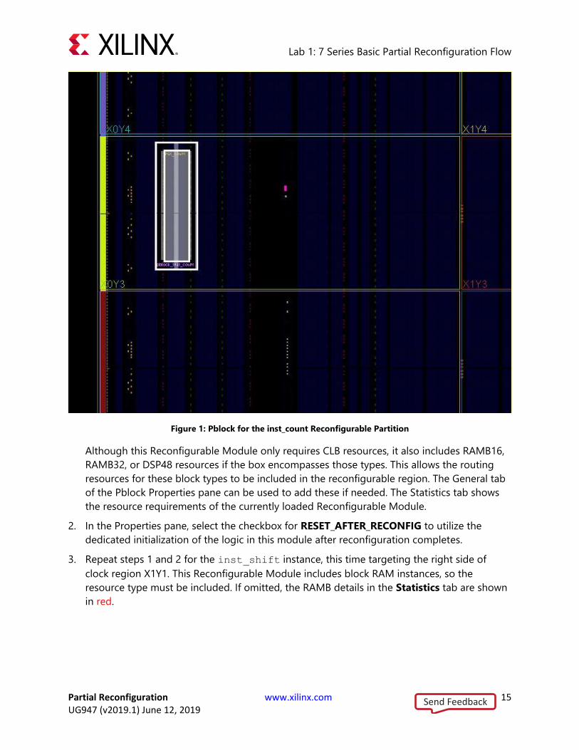
1. Select the inst_count instance in the Netlist pane. Right-click and select Floorplanning >
Draw Pblock, or select the Draw Pblock toolbar button , and draw a tall narrow box on
the left side of the X0Y3 clock region. The exact size and shape do not matter at this point,
but keep the box within the clock region.
Make sure that the Pblock is selected in the Device View before continuing.
Send Feedback
Lab 1: 7 Series Basic Partial Reconfiguration Flow
Partial Reconfiguration www.xilinx.com 15 UG947 (v2019.1) June 12, 2019
Figure 1: Pblock for the inst_count Reconfigurable Partition
Although this Reconfigurable Module only requires CLB resources, it also includes RAMB16,
RAMB32, or DSP48 resources if the box encompasses those types. This allows the routing
resources for these block types to be included in the reconfigurable region. The General tab
of the Pblock Properties pane can be used to add these if needed. The Statistics tab shows
the resource requirements of the currently loaded Reconfigurable Module.
2. In the Properties pane, select the checkbox for RESET_AFTER_RECONFIG to utilize the
dedicated initialization of the logic in this module after reconfiguration completes.
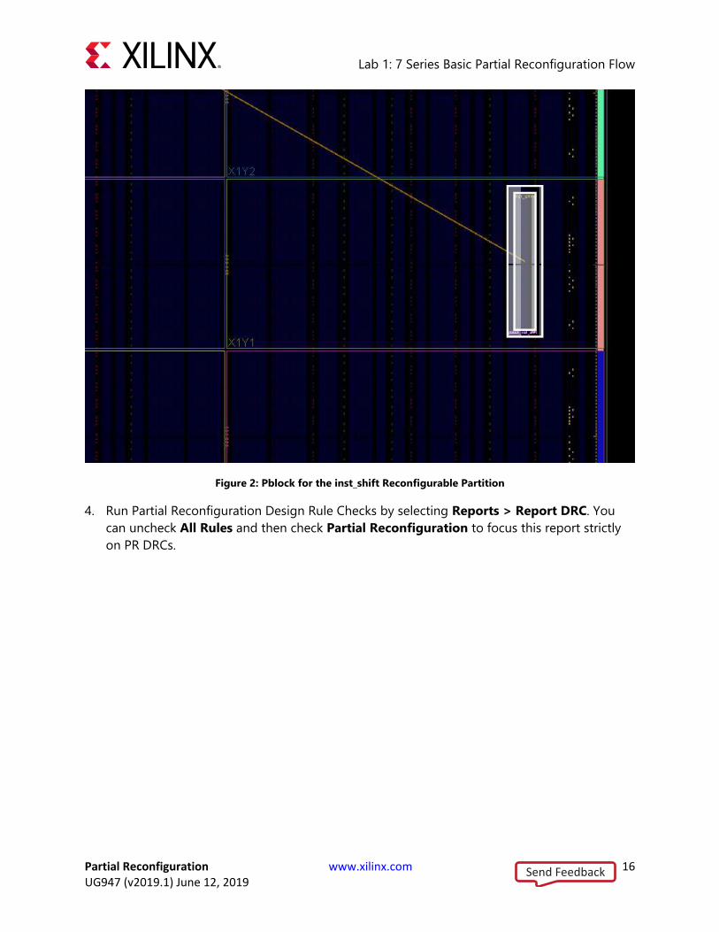
3. Repeat steps 1 and 2 for the inst_shift instance, this time targeting the right side of
clock region X1Y1. This Reconfigurable Module includes block RAM instances, so the
resource type must be included. If omitted, the RAMB details in the Statistics tab are shown
in red.
Send Feedback
Lab 1: 7 Series Basic Partial Reconfiguration Flow
Partial Reconfiguration www.xilinx.com 16 UG947 (v2019.1) June 12, 2019
Figure 2: Pblock for the inst_shift Reconfigurable Partition
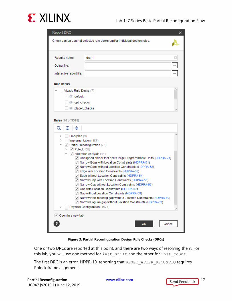
4. Run Partial Reconfiguration Design Rule Checks by selecting Reports > Report DRC. You
can uncheck All Rules and then check Partial Reconfiguration to focus this report strictly
on PR DRCs.
Send Feedback
Lab 1: 7 Series Basic Partial Reconfiguration Flow
Partial Reconfiguration www.xilinx.com 17 UG947 (v2019.1) June 12, 2019
Figure 3: Partial Reconfiguration Design Rule Checks (DRCs)
One or two DRCs are reported at this point, and there are two ways of resolving them. For
this lab, you will use one method for inst_shift and the other for inst_count.
The first DRC is an error, HDPR-10, reporting that RESET_AFTER_RECONFIG requires
Pblock frame alignment.
Send Feedback
Lab 1: 7 Series Basic Partial Reconfiguration Flow
Partial Reconfiguration www.xilinx.com 18 UG947 (v2019.1) June 12, 2019
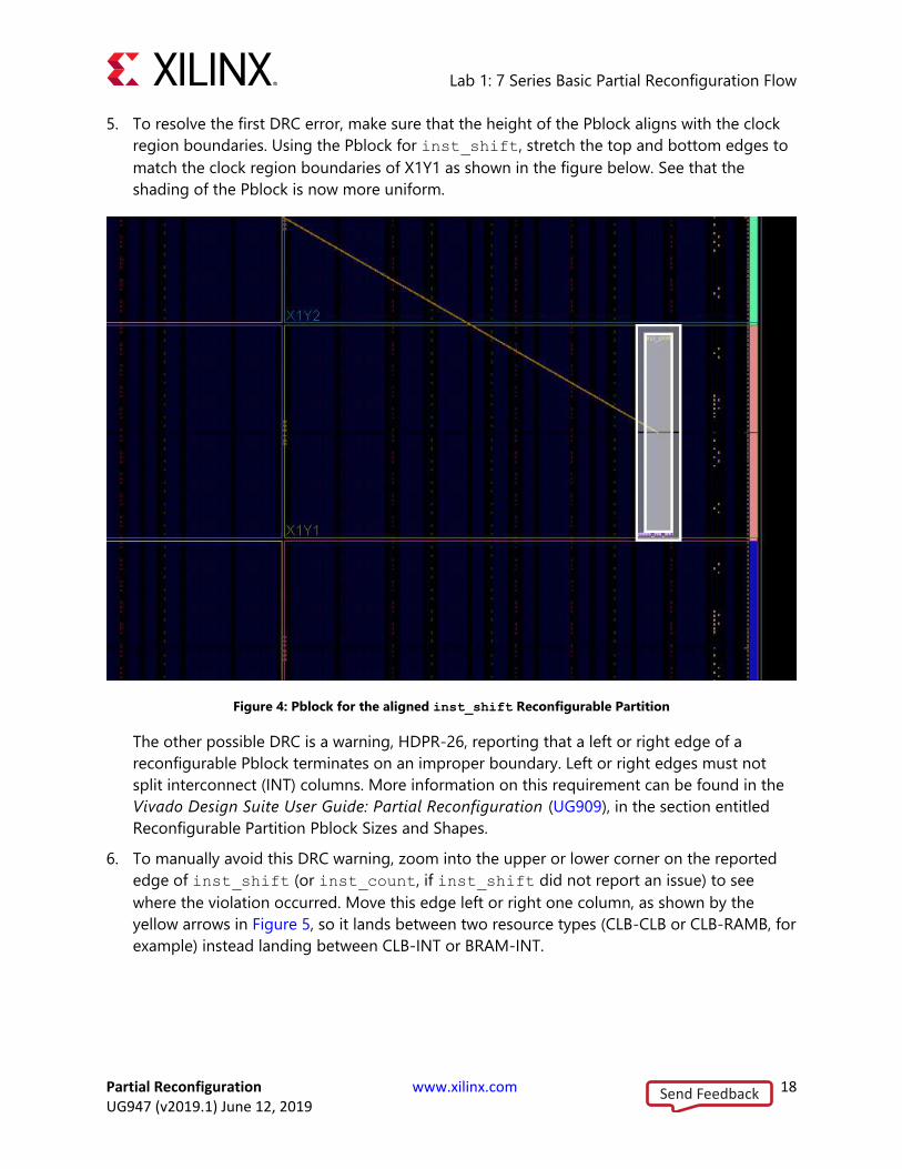
5. To resolve the first DRC error, make sure that the height of the Pblock aligns with the clock
region boundaries. Using the Pblock for inst_shift, stretch the top and bottom edges to
match the clock region boundaries of X1Y1 as shown in the figure below. See that the
shading of the Pblock is now more uniform.
Figure 4: Pblock for the aligned inst_shift Reconfigurable Partition
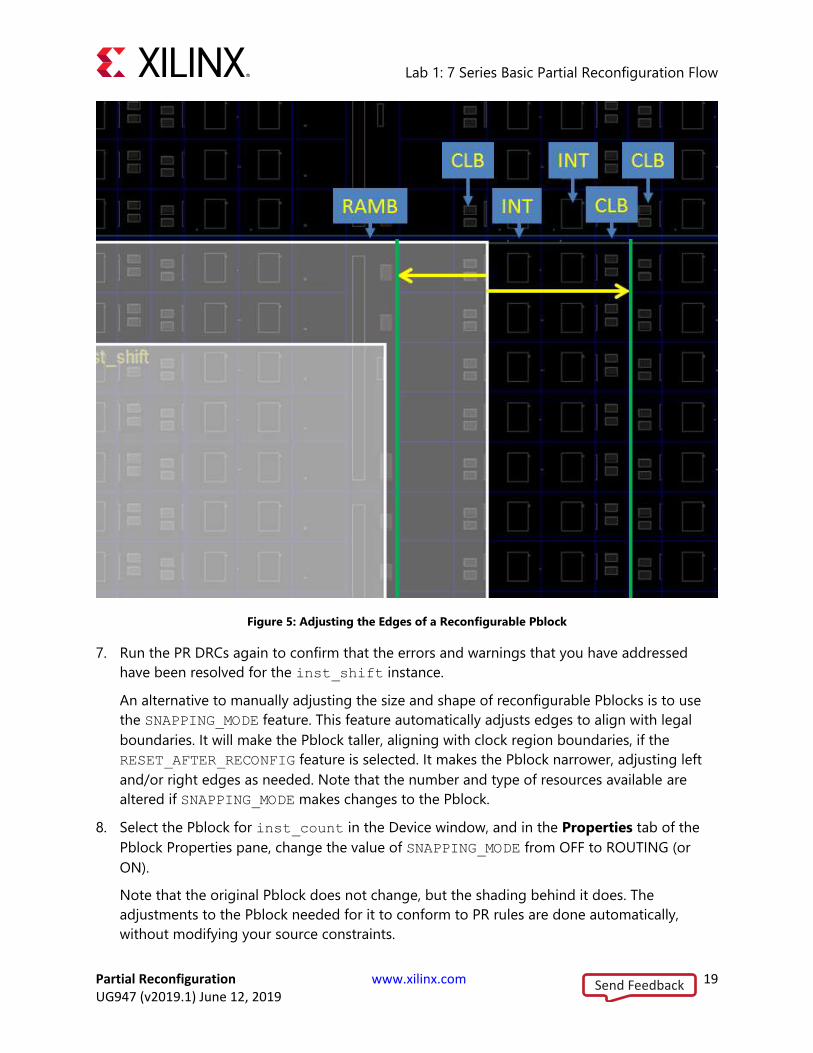
The other possible DRC is a warning, HDPR-26, reporting that a left or right edge of a
reconfigurable Pblock terminates on an improper boundary. Left or right edges must not
split interconnect (INT) columns. More information on this requirement can be found in the
Vivado Design Suite User Guide: Partial Reconfiguration (UG909), in the section entitled
Reconfigurable Partition Pblock Sizes and Shapes.
6. To manually avoid this DRC warning, zoom into the upper or lower corner on the reported
edge of inst_shift (or inst_count, if inst_shift did not report an issue) to see
where the violation occurred. Move this edge left or right one column, as shown by the
yellow arrows in Figure 5, so it lands between two resource types (CLB-CLB or CLB-RAMB, for
example) instead landing between CLB-INT or BRAM-INT.
Send Feedback
Lab 1: 7 Series Basic Partial Reconfiguration Flow
Partial Reconfiguration www.xilinx.com 19 UG947 (v2019.1) June 12, 2019
Figure 5: Adjusting the Edges of a Reconfigurable Pblock
7. Run the PR DRCs again to confirm that the errors and warnings that you have addressed
have been resolved for the inst_shift instance.
An alternative to manually adjusting the size and shape of reconfigurable Pblocks is to use
the SNAPPING_MODE feature. This feature automatically adjusts edges to align with legal
boundaries. It will make the Pblock taller, aligning with clock region boundaries, if the
RESET_AFTER_RECONFIG feature is selected. It makes the Pblock narrower, adjusting left
and/or right edges as needed. Note that the number and type of resources available are
altered if SNAPPING_MODE makes changes to the Pblock.
8. Select the Pblock for inst_count in the Device window, and in the Properties tab of the
Pblock Properties pane, change the value of SNAPPING_MODE from OFF to ROUTING (or
ON).
Note that the original Pblock does not change, but the shading behind it does. The
adjustments to the Pblock needed for it to conform to PR rules are done automatically,
without modifying your source constraints.
Send Feedback
Lab 1: 7 Series Basic Partial Reconfiguration Flow
Partial Reconfiguration www.xilinx.com 20 UG947 (v2019.1) June 12, 2019
9. Run the PR DRCs once again to confirm that all errors have been resolved. Advisory
messages may still be reported, especially if the Pblock is located near the edge of the
device.
10. Save these Pblocks and associated properties:
write_xdc ./Sources/xdc/top_all.xdc
This exports all the current constraints in the design, including those imported earlier from
top_io_$board.xdc. These constraints can be managed in their own XDC file or managed
within a run script (as is typically done with HD.RECONFIGURABLE).
Alternatively, the Pblock constraints themselves can be extracted and managed separately. A
Tcl proc is available to help perform this task.
a. First source the proc which is found in one of the Tcl utility files:
source ./Tcl_HD/hd_utils.tcl
b. Then use the export_pblocks proc to write out this constraint information:
export_pblocks -file ./Sources/xdc/pblocks.xdc
This writes the Pblock constraint information for both Pblocks in the design. Use the
-pblocks option to select only one if desired.
Now that the floorplan is established, the next step is implementing the design.
Step 6: Implementing the First Configuration In this step, you place and route the design and prepare the static portion of the design for
reuse with new Reconfigurable Modules.
Implementing the Design
1. Optimize, place, and route the design by issuing the following command:
opt_design
This is the point at which the Partial Reconfiguration license is checked. If you have a valid
license, you see this message:
Feature available: PartialReconfiguration
If you have no license with the PartialReconfiguration feature, contact your local
Xilinx sales office for more information. Evaluation licenses are available.
place_design
route_design
Send Feedback
Lab 1: 7 Series Basic Partial Reconfiguration Flow
Partial Reconfiguration www.xilinx.com 21 UG947 (v2019.1) June 12, 2019
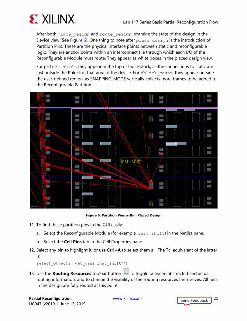
After both place_design and route_design, examine the state of the design in the
Device view (See Figure 6). One thing to note after place_design is the introduction of
Partition Pins. These are the physical interface points between static and reconfigurable
logic. They are anchor points within an interconnect tile through which each I/O of the
Reconfigurable Module must route. They appear as white boxes in the placed design view.
For pblock_shift, they appear in the top of that Pblock, as the connections to static are
just outside the Pblock in that area of the device. For pblock_count, they appear outside
the user-defined region, as SNAPPING_MODE vertically collects more frames to be added to
the Reconfigurable Partition.
Figure 6: Partition Pins within Placed Design
11. To find these partition pins in the GUI easily:
a. Select the Reconfigurable Module (for example, inst_shift) in the Netlist pane.
b. Select the Cell Pins tab in the Cell Properties pane.
12. Select any pin to highlight it, or use Ctrl+A to select them all. The Tcl equivalent of the latter
is:
select_objects [get_pins inst_shift/*]
13. Use the Routing Resources toolbar button to toggle between abstracted and actual
routing information, and to change the visibility of the routing resources themselves. All nets
in the design are fully routed at this point.
Send Feedback

Lab 1: 7 Series Basic Partial Reconfiguration Flow
Partial Reconfiguration www.xilinx.com 22 UG947 (v2019.1) June 12, 2019
Figure 7: Close-up of First Configuration Routed
Saving the Results
14. Save the full design checkpoint and create report files by issuing these commands:
write_checkpoint -force Implement/Config_shift_right_count_up_implement/top_route_design.dcp
report_utilization -file Implement/Config_shift_right_count_up_implement/top_utilization.rpt
report_timing_summary -file Implement/Config_shift_right_count_up_implement/top_timing_summary.rpt
15. [Optional] Save checkpoints for each of the Reconfigurable Modules by issuing these two
commands:
write_checkpoint -force -cell inst_shift Checkpoint/shift_right_route_design.dcp
write_checkpoint -force -cell inst_count Checkpoint/count_up_route_design.dcp
TIP: When running run_pr.tcl to process the entire design in batch mode; design
checkpoints, log files, and report files are created at each step of the flow.
At this point, you have created a fully implemented partial reconfiguration design from
which you can generate full and partial bitstreams. The static portion of this configuration is
used for all subsequent configurations. To isolate the static design, remove the current
Reconfigurable Modules. Make sure routing resources are enabled, and zoom in to an
interconnect tile with partition pins.
Send Feedback
Lab 1: 7 Series Basic Partial Reconfiguration Flow
Partial Reconfiguration www.xilinx.com 23 UG947 (v2019.1) June 12, 2019
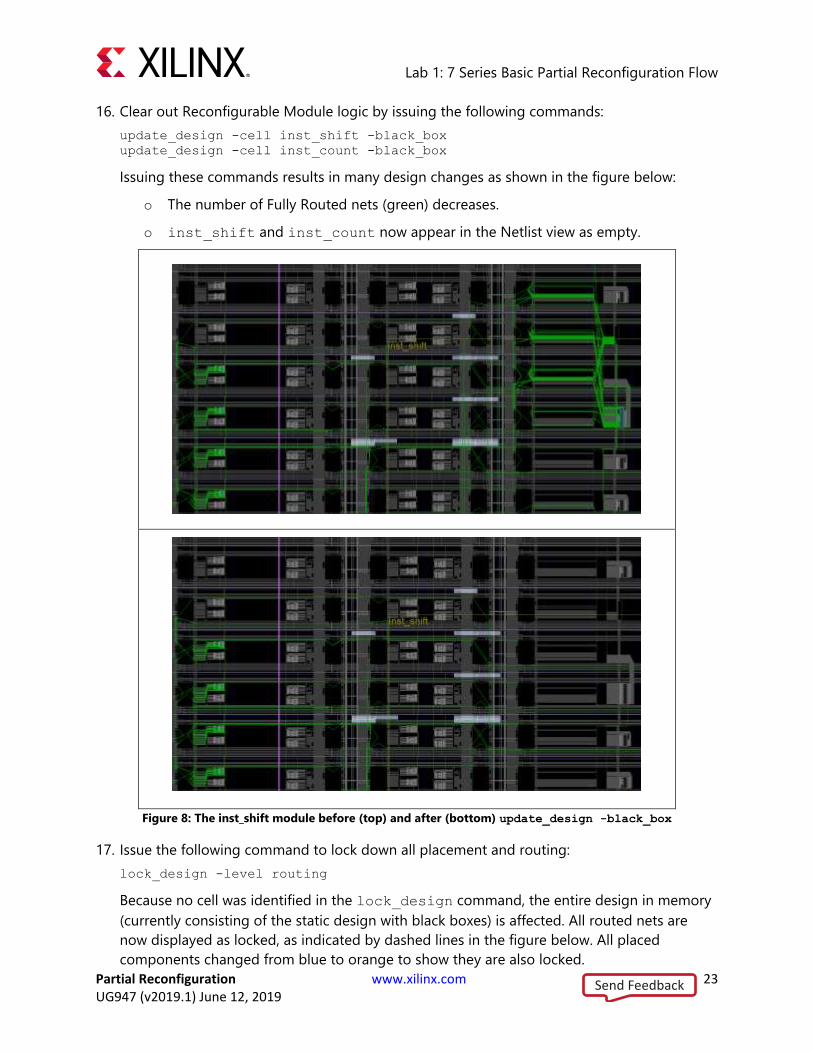
16. Clear out Reconfigurable Module logic by issuing the following commands:
update_design -cell inst_shift -black_box
update_design -cell inst_count -black_box
Issuing these commands results in many design changes as shown in the figure below:
o The number of Fully Routed nets (green) decreases.
o inst_shift and inst_count now appear in the Netlist view as empty.
Figure 8: The inst_shift module before (top) and after (bottom) update_design -black_box
17. Issue the following command to lock down all placement and routing:
lock_design -level routing
Because no cell was identified in the lock_design command, the entire design in memory
(currently consisting of the static design with black boxes) is affected. All routed nets are
now displayed as locked, as indicated by dashed lines in the figure below. All placed
components changed from blue to orange to show they are also locked.
Send Feedback

Lab 1: 7 Series Basic Partial Reconfiguration Flow
Partial Reconfiguration www.xilinx.com 24 UG947 (v2019.1) June 12, 2019
Figure 9: Close-up of Static-Only Design with Locked Routing
18. Issue the following command to write out the remaining static-only checkpoint:
write_checkpoint -force Checkpoint/static_route_design.dcp
This static-only checkpoint is used for future configurations.
19. Close this design before moving on to the next configuration:
close_project
Send Feedback

Lab 1: 7 Series Basic Partial Reconfiguration Flow
Partial Reconfiguration www.xilinx.com 25 UG947 (v2019.1) June 12, 2019
Step 7: Implementing the Second Configuration Now that the static design result is established and locked, and you can use it as context for
implementing further Reconfigurable Modules.
Implementing the Design
1. Create a new in-memory design by issuing the following command in the Tcl Console:
create_project -in_memory -part $part
2. Load the static design by issuing the following command:
add_files ./Checkpoint/static_route_design.dcp
3. Load the second two synthesis checkpoints for the shift and count functions by issuing these
commands:
add_files ./Synth/shift_left/shift_synth.dcp
set_property SCOPED_TO_CELLS {inst_shift} [get_files ./Synth/shift_left/shift_synth.dcp]
add_files ./Synth/count_down/count_synth.dcp
set_property SCOPED_TO_CELLS {inst_count} [get_files ./Synth/count_down/count_synth.dcp]
4. Link the entire design together using the link_design command:
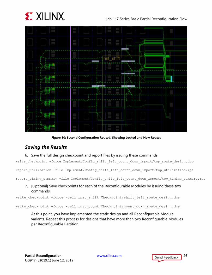
link_design -mode default -reconfig_partitions {inst_shift inst_count} -part $part -top top
At this point, a full configuration is loaded. This time, however, the static design is routed
and locked, and the reconfigurable logic is still just a netlist. Place and route from here only
applies to the RM logic.
5. Optimize, place and route the new RMs in the context of static by issuing these commands:
opt_design
place_design
route_design
The design is again fully implemented, now with the new Reconfigurable Module variants.
The routing is a mix of dashed (locked) and solid (new) routing segments, as shown below.
Send Feedback
Lab 1: 7 Series Basic Partial Reconfiguration Flow
Partial Reconfiguration www.xilinx.com 26 UG947 (v2019.1) June 12, 2019
Figure 10: Second Configuration Routed, Showing Locked and New Routes
Saving the Results
6. Save the full design checkpoint and report files by issuing these commands:
write_checkpoint -force Implement/Config_shift_left_count_down_import/top_route_design.dcp
report_utilization -file Implement/Config_shift_left_count_down_import/top_utilization.rpt
report_timing_summary -file Implement/Config_shift_left_count_down_import/top_timing_summary.rpt
7. [Optional] Save checkpoints for each of the Reconfigurable Modules by issuing these two
commands:
write_checkpoint -force -cell inst_shift Checkpoint/shift_left_route_design.dcp
write_checkpoint -force -cell inst_count Checkpoint/count_down_route_design.dcp
At this point, you have implemented the static design and all Reconfigurable Module
variants. Repeat this process for designs that have more than two Reconfigurable Modules
per Reconfigurable Partition.
Send Feedback

Lab 1: 7 Series Basic Partial Reconfiguration Flow
Partial Reconfiguration www.xilinx.com 27 UG947 (v2019.1) June 12, 2019
Step 8: Examining the Results with Highlighting Scripts With the routed configuration open in the IDE, run some visualization scripts to highlight tiles
and nets. These scripts identify the resources allocated for partial reconfiguration, and are
automatically generated.
1. In the Tcl Console, issue the following commands from the <Extract_Dir> directory:
source hd_visual/pblock_inst_shift_AllTiles.tcl
highlight_objects -color blue [get_selected_objects]
2. Click somewhere in the Device view to deselect the frames (or enter unselect_objects),
then issue the following commands:
source hd_visual/pblock_inst_count_AllTiles.tcl
highlight_objects -color yellow [get_selected_objects]
The partition frames appear highlighted in the Device view, as shown in Figure 11.
Figure 11: Reconfigurable Partition Frames Highlighted
Send Feedback
Lab 1: 7 Series Basic Partial Reconfiguration Flow
Partial Reconfiguration www.xilinx.com 28 UG947 (v2019.1) June 12, 2019
These highlighted tiles represent the configuration frames that are sent to bitstream
generation to create the partial bitstreams. As shown above, the SNAPPING_MODE feature
adjusted all four edges of pblock_count to account for RESET_AFTER_RECONFIG and
legal reconfigurable partition widths.
The other “tile” scripts are variations on these. If you had not created Pblocks that vertically
aligned to the clock region boundaries, the FrameTiles script would highlight the explicit
Pblock tiles, while the AllTiles script extends those tiles to the full reconfigurable frame
height. Note that these leave gaps where unselected frame types (for example: global clocks)
exist.
The GlitchTiles script is a subset of frame sites, avoiding dedicated silicon resources; the
other scripts are more informative than this one.
3. Close the current design:
close_project
Step 9: Generating Bitstreams
Verifying Configurations
RECOMMENDED: Before generating bitstreams, verify all configurations to ensure
that the static portion of each configuration match identically, so the resulting
bitstreams are safe to use in silicon. The PR Verify feature examines the complete static
design up to and including the partition pins, confirming that they are identical.
Placement and routing within the Reconfigurable Modules is not checked, as different
module results are expected here.
1. Run the pr_verify command from the Tcl Console:
pr_verify Implement/Config_shift_right_count_up_implement/top_route_design.dcp
Implement/Config_shift_left_count_down_import/top_route_design.dcp
If successful, this command returns the following message.
INFO: [Vivado 12-3253] PR_VERIFY: check points
Implement/Config_shift_right_count_up/top_route_design.dcp and
Implement/Config_shift_left_count_down/top_route_design.dcp are compatible
By default, only the first mismatch (if any) is reported. To see all mismatches, use the
-full_check option.
2. Close the project:
close_project
Send Feedback
Lab 1: 7 Series Basic Partial Reconfiguration Flow
Partial Reconfiguration www.xilinx.com 29 UG947 (v2019.1) June 12, 2019
Generating Bitstreams
Now that the configurations have been verified, you can generate bitstreams and use them to
target your selected demonstration board.
Note: The first configuration implements shift_right and count_up. The second
configuration implements shift_left and count_down.
3. First, read the first configuration into memory:
open_checkpoint Implement/Config_shift_right_count_up_implement/top_route_design.dcp
4. Generate full and partial bitstreams for this design. Be sure to keep the bit files in a unique
directory related to the full design checkpoint from which they were created.
write_bitstream -force -file Bitstreams/Config_RightUp.bit
close_project
Notice that three bitstreams have been created:
o Config_RightUp.bit
This is the power-up, full design bitstream. The four shift LEDs on the right will shift
right and the four count LEDs on the left will count up.
o Config_RightUp_pblock_inst_shift_partial.bit
This is the partial bit file for the shift_right module.
o Config_RightUp_pblock_inst_count_partial.bit
This is the partial bit file for the count_up module that causes the count LEDs to
count up.
IMPORTANT: When generated by a single call to write_bitstream, the names of
the bit files currently do not reflect the name of the Reconfigurable Module variant to
clarify which image is loaded. The current solution uses the base name given by the -
file option and appends the Pblock name of the reconfigurable cell. It is critical to
provide enough description in the base name to be able to identify the reconfigurable
bit files clearly. All partial bit files have the _partial postfix.
Using run_pr.tcl to process the entire design through bitstream generation uses a
different technique for generating the bitstreams. Opening a routed design checkpoint
issues multiple calls to write_bitstream, which gives you more control over naming
bitstreams and allows for different options (such a bitstream compression) to be applied to
full versus partial bitstreams. For example, the names configured in the
advanced_settings.tcl script are:
o Config_shift_right_count_up_implement_full.bit
This is the power-up, full design bitstream.
o pblock_shift_shift_right_partial.bit
This is the partial bit file for the shift_right module.
Send Feedback

Lab 1: 7 Series Basic Partial Reconfiguration Flow
Partial Reconfiguration www.xilinx.com 30 UG947 (v2019.1) June 12, 2019
o pblock_count_count_up_partial.bit
This is the partial bit file for the count_up module.
5. Generate full and partial bitstreams for the second configuration, again keeping the resulting
bit files in the appropriate folder.
open_checkpoint Implement/Config_shift_left_count_down_import/top_route_design.dcp
write_bitstream -force -file Bitstreams/Config_LeftDown.bit
close_project
Similarly, you see three bitstreams created, this time with a different base name.
6. Generate a full bitstream with grey boxes, plus blanking bitstreams for the Reconfigurable
Modules. Blanking bitstreams can be used to “erase” an existing configuration to reduce
power consumption.
open_checkpoint Checkpoint/static_route_design.dcp
update_design -cell inst_count -buffer_ports
update_design -cell inst_shift -buffer_ports
place_design
route_design
write_checkpoint -force Checkpoint/Config_greybox.dcp
write_bitstream -force -file Bitstreams/config_greybox.bit
close_project
The base configuration bitstream has no logic for either reconfigurable partition. The
update_design commands here insert constant drivers (ground) for all outputs of the
Reconfigurable Partitions, so these outputs do not float. The term grey box indicates that the
modules are not completely empty with these LUTs inserted, as opposed to black boxes,
which would have dangling nets in and out of this region. The place_design and
route_design commands ensure they are completely implemented.
Step 10: Partially Reconfiguring the FPGA The count_shift_led design targets one of four demonstration boards. The current design
supports the KC705, VC707, VC709 and AC701 boards, revisions Rev 1.0 and Rev 1.1.
Send Feedback
Lab 1: 7 Series Basic Partial Reconfiguration Flow
Partial Reconfiguration www.xilinx.com 31 UG947 (v2019.1) June 12, 2019
Configuring the Device with a Full Image
1. Connect the board to your computer via the Platform Cable USB and power on the board.
2. From the main Vivado IDE, select Flow > Open Hardware Manager.
3. Select Open a new hardware target on the green banner. Follow the steps in the wizard to
establish communication with the board.
4. Select Program device on the green banner, and select the target device. Navigate to the
Bitstreams folder to select Config_RightUp.bit, then click OK to program the device.
You should now see the bank of GPIO LEDs performing two tasks. Four LEDs are performing
a counting-up function (MSB is on the left), and the other four are shifting to the right. Note
the amount of time it took to configure the full device.
Note: The AC701 demonstration board only has a 4-bit LED bank. This design will show
either the shift function or the count function at one time. To switch between the shift and
count functions, toggle the switch 1 on the GPIO DIP switch (SW2).
Partially Reconfiguring the Device
At this point, you can partially reconfigure the active device with any of the partial bitstreams
that you have created.
5. Select Program device on the green banner again. Navigate to the Bitstreams folder to
select Config_LeftDown_pblock_inst_shift_partial.bit, then click OK to
program the device.
The shift portion of the LEDs changed direction, but the counter kept counting up,
unaffected by the reconfiguration. Note the much shorter configuration time.
6. Select Program device on the green banner again. Navigate to the Bitstreams folder to
select Config_LeftDown_pblock_inst_count_partial.bit, then click OK to
program the device.
The counter is now counting down, and the shifting LEDs were unaffected by the
reconfiguration. This process can be repeated with the Config_RightUp partial bit files to
return to the original configuration, or with the blanking (grey box) partial bit files to stop
activity on the LEDs (that will stay on).
Send Feedback
Lab 1: 7 Series Basic Partial Reconfiguration Flow
Partial Reconfiguration www.xilinx.com 32 UG947 (v2019.1) June 12, 2019
Conclusion This concludes Lab 1. In this lab, you:
• Synthesized a design bottom-up to prepare for partial reconfiguration implementation
• Created a valid floorplan for a partial reconfiguration design
• Created two configurations with common static results
• Implemented these two configurations, saving the static design to be used in each
• Created checkpoints for static and reconfigurable modules for later reuse
• Examined framesets and verified the two configurations
• Created full and partial bitstreams
• Configured and partially reconfigured an FPGA
Send Feedback
Partial Reconfiguration www.xilinx.com 33 UG947 (v2019.1) June 12, 2019
Lab 2: UltraScale Basic Partial Reconfiguration Flow
Overview This lab introduces the basic PR flow for UltraScale devices. First, you will use a script to
individually synthesize the static module and each reconfigurable design module variant. Then
in the IDE, you will constrain the location of the reconfigurable modules (RM) using Pblocks and
implement the initial configuration of the design. Next, you will implement alternate
configurations by locking the static portion of the design, updating the reconfigurable modules
with a variant, and re-running implementation. Finally, you will verify that each implemented RM
is compatible with the static portion of the design and, if compatible, generate bitstreams.
Step 1: Extracting the Tutorial Design Files 1. To obtain the tutorial design file, see the Tutorial Design Description.
2. Navigate to \led_shift_count_us in the extracted files. The led_shift_count_us
data directory is referred to in this lab as the <Extract_Dir>.
Step 2: Examining the Scripts Start by reviewing the scripts provided in the design archive. The files run_pr.tcl and
advanced_settings.tcl are located at the root level. The run_pr.tcl script contains the
minimum required settings to run partial reconfiguration. The advanced_settings.tcl
contains default flow settings and should only be modified by experienced users.
The Main Script
In the <Extract_Dir>, open run_pr.tcl in a text editor. This is the master script where you
define the design parameters, design sources, and design structure. This is the only file you have
to modify to compile a complete Partial Reconfiguration design. Find more details regarding
run_pr.tcl, advanced_settings.tcl, and the underlying scripts in the README.txt
located in the Tcl_HD subdirectory.
Note the following details in this run_pr.tcl:
• Under Define target demo board, you can select one of many demonstration boards
supported for this design.
• Under flow control, you can control what phases of synthesis and implementation are
run. In the tutorial, only synthesis is run by the script; implementation, verification, and
Send Feedback
Lab 2: UltraScale Basic Partial Reconfiguration Flow
Partial Reconfiguration www.xilinx.com 34 UG947 (v2019.1) June 12, 2019
bitstream generation are run interactively. To run these additional steps via the script, set
the flow variables (e.g., run.prImpl) to 1.
• The Output Directories and Input Directories set the file structure expected for design
sources and results files. You must reflect any changes to your file structure here.
• The Top Definition and RP Module Definitions sections let you reference all source
files for each part of your design. Top Definition covers all sources needed for the static
design, including constraints and IP. The RP Module Definitions section does the same
for Reconfigurable Partitions (RP). Identify each RP and list all Reconfigurable Module
(RM) variants for each RP.
o This design has two Reconfigurable Partitions (inst_shift and inst_count), and
each RP has two module variants.
• The Configuration Definition sections define the sets of static and reconfigurable
modules that make up a configuration.
o This design has two configurations defined within the master script:
config_shift_right_count_up_implement and
config_shift_left_count_down_import.
o You can create more configurations by adding RMs or by combining existing RMs.
The Supporting Scripts
Underneath the Tcl_HD subdirectory, several supporting Tcl scripts exist. The scripts are called
by run_pr.tcl, and they manage specific details for the Partial Reconfiguration flow. Provided
below are some details about a few of the key PR scripts.
CAUTION! Do not modify the supporting Tcl scripts.
• step.tcl
Manages the current status of the design by monitoring checkpoints.
• synthesize.tcl
Manages all the details regarding the synthesis phase.
• implement.tcl
Manages all the details regarding the module implementation phase.
• pr_utils.tcl
Manages all the details regarding the top-level implementation of a PR design.
• run.tcl
Launches the actual runs for synthesis and implementation.
• log_utils.tcl
Handles report file creation at key points during the flow.
Send Feedback

Lab 2: UltraScale Basic Partial Reconfiguration Flow
Partial Reconfiguration www.xilinx.com 35 UG947 (v2019.1) June 12, 2019
Remaining scripts provide details within these scripts (such as other *_utils.tcl scripts) or
manage other Hierarchical Design flows (such as hd_utils.tcl).
Step 3: Synthesizing the Design The run_pr.tcl script automates the synthesis phase of this tutorial. Five iterations of
synthesis are called, one for the static top-level design and one for each of four Reconfigurable
Modules.
1. Open the Vivado Tcl shell:
o On Windows, select the Xilinx Vivado desktop icon or Start > All Programs > Xilinx
Design Tools> Vivado 2018.x > Vivado 2018.x Tcl Shell.
o On Linux, type: vivado -mode tcl.
2. In the shell, navigate to the <Extract_Dir> directory.
3. If you are using a target demonstration board other than the KCU105, modify the xboard
variable in run_pr.tcl. The alternative for this lab is the VCU108 board.
4. Run the run_pr.tcl script by entering:
source run_pr.tcl -notrace
After all five passes through Vivado Synthesis have completed, the Vivado Tcl shell is left open.
You can find log and report files for each module, alongside the final checkpoints, under each
named folder in the Synth subdirectory.
TIP: In the <Extract_Dir> directory, multiple log files have been created:
• run.log shows the summary as posted in the Tcl shell window
• command.log echoes all the individual steps run by the script
• critical.log reports all critical warnings produced during the run.
Step 4: Assembling and Implementing the Design Now that the synthesized checkpoints for each module, plus top, are available, you can
assemble the design.
You will run all flow steps from the Tcl Console, but you can use features within the IDE (such as
the floorplanning tool) for interactive events.
TIP: Copy and paste commands directly from this document to avoid redundant effort
and typos in the Vivado IDE. Copy and paste only one full command at a time. Note
that some commands are long and therefore span multiple lines.
Send Feedback
Lab 2: UltraScale Basic Partial Reconfiguration Flow
Partial Reconfiguration www.xilinx.com 36 UG947 (v2019.1) June 12, 2019
1. Open the Vivado IDE. You can open the IDE from the open Tcl shell by typing start_gui or
by launching Vivado with the command vivado -mode gui.
2. Navigate to the <Extract_Dir> directory if you are not already there. The pwd command
can confirm this.
3. Set variables that help with copying commands from this document into the Tcl Console.
Select the part and board you are targeting for this lab, and apply them in Vivado:
set part "xcku040-ffva1156-2-e"
set board "kcu105"
set part "xcvu095-ffva2104-2-e"
set board "vcu108"
set part "xcku5p-ffvb676-2-e"
set board "kcu116"
set part "xcvu9p-flga2104-2L-e"
set board "vcu118"
4. Create an in-memory design by issuing the following command in the Tcl Console:
create_project -in_memory -part $part
5. Load the static design by issuing the following command:
add_files ./Synth/Static/top_synth.dcp
6. Load the top-level design constraints by issuing these commands:
add_files ./Sources/xdc/top_io_$board.xdc
set_property USED_IN {implementation} [get_files ./Sources/xdc/top_io_$board.xdc]
Selecting the top_io_$board version of the available xdc file loads the pin location and
clocking constraints, but does not include floorplan information. The top_$board version
includes pin location, clocking and floorplanning constraints.
7. Load the first two synthesis checkpoints for the shift and count functions by issuing these
commands:
add_file ./Synth/shift_right/shift_synth.dcp
set_property SCOPED_TO_CELLS {inst_shift} [get_files ./Synth/shift_right/shift_synth.dcp]
add_file ./Synth/count_up/count_synth.dcp
set_property SCOPED_TO_CELLS {inst_count} [get_files ./Synth/count_up/count_synth.dcp]
The SCOPED_TO_CELLS property ensures that the proper assignment is made to the target
cell. See this link in Vivado Design Suite User Guide: Using Constraints (UG903) for more
information.
8. Link the entire design together using the link_design command:
link_design -mode default -reconfig_partitions {inst_shift inst_count} -part $part -top top
Send Feedback
Lab 2: UltraScale Basic Partial Reconfiguration Flow
Partial Reconfiguration www.xilinx.com 37 UG947 (v2019.1) June 12, 2019
At this point a full configuration is loaded, including static and reconfigurable logic. Note
that the Flow Navigator pane is not present while you are working in non-project mode.
TIP: Place the IDE in floorplanning mode by selecting Layout > Floorplanning. Make
sure the Device view is visible.
9. Save the assembled design state for this initial configuration:
write_checkpoint ./Checkpoint/top_link_right_up.dcp
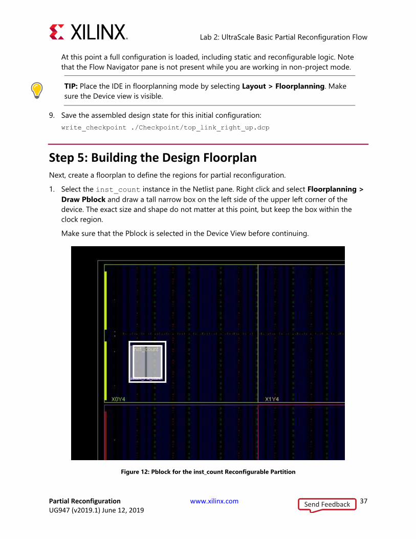
Step 5: Building the Design Floorplan Next, create a floorplan to define the regions for partial reconfiguration.
1. Select the inst_count instance in the Netlist pane. Right click and select Floorplanning >
Draw Pblock and draw a tall narrow box on the left side of the upper left corner of the
device. The exact size and shape do not matter at this point, but keep the box within the
clock region.
Make sure that the Pblock is selected in the Device View before continuing.
Figure 12: Pblock for the inst_count Reconfigurable Partition
Send Feedback

Lab 2: UltraScale Basic Partial Reconfiguration Flow
Partial Reconfiguration www.xilinx.com 38 UG947 (v2019.1) June 12, 2019
Although this Reconfigurable Module only requires CLB resources, also include RAMB16,
RAMB32, or DSP48 resources if the box encompasses those types. This allows the routing
resources for these block types to be included in the reconfigurable region. The General tab
of the Pblock Properties pane can be used to add these if needed. The Statistics tab shows
the resource requirements of the currently loaded Reconfigurable Module.
2. Repeat the previous step for the inst_shift instance, this time targeting clock region
below the first. This Reconfigurable Module includes block RAM instances, so the resource
type must be included. If omitted, the RAMB details in the Statistics tab will be shown in
red.
Figure 13: Pblock for the inst_shift Reconfigurable Partition
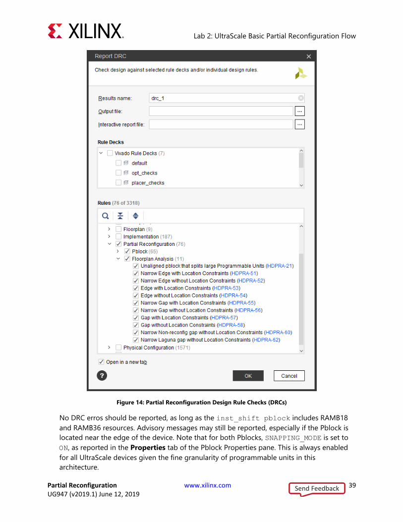
3. Run Partial Reconfiguration Design Rule Checks by selecting Reports > Report DRC. You
can uncheck All Rules and then check Partial Reconfiguration to focus this report strictly
on PR DRCs.
Send Feedback
Lab 2: UltraScale Basic Partial Reconfiguration Flow
Partial Reconfiguration www.xilinx.com 39 UG947 (v2019.1) June 12, 2019
Figure 14: Partial Reconfiguration Design Rule Checks (DRCs)
No DRC erros should be reported, as long as the inst_shift pblock includes RAMB18
and RAMB36 resources. Advisory messages may still be reported, especially if the Pblock is
located near the edge of the device. Note that for both Pblocks, SNAPPING_MODE is set to
ON, as reported in the Properties tab of the Pblock Properties pane. This is always enabled
for all UltraScale devices given the fine granularity of programmable units in this
architecture.
Send Feedback

Lab 2: UltraScale Basic Partial Reconfiguration Flow
Partial Reconfiguration www.xilinx.com 40 UG947 (v2019.1) June 12, 2019
4. Save these Pblocks and associated properties:
write_xdc ./Sources/xdc/top_all.xdc
This exports all the current constraints in the design, including those imported earlier from
top_io_$board.xdc. These constraints can be managed in their own XDC file or managed
within a run script (as is typically done with HD.RECONFIGURABLE).
Alternatively, the Pblock constraints themselves can be extracted and managed separately. A
Tcl proc is available to help perform this task.
a. First source the proc which is found in one of the Tcl utility files:
source ./Tcl_HD/hd_utils.tcl
b. Then use the export_pblocks proc to write out this constraint information:
export_pblocks -file ./Sources/xdc/pblocks.xdc
This writes the Pblock constraint information for both Pblocks in the design. Use the
-pblocks option to select only one if desired.
Step 6: Implementing the First Configuration In this step, you place and route the design and prepare the static portion of the design for
reuse with new Reconfigurable Modules.
Implementing the Design
1. Optimize, place, and route the design by issuing the following commands:
opt_design
This is the point at which the Partial Reconfiguration license is checked. If you have a valid
license, you see this message:
Feature available: PartialReconfiguration
If you have no license with the PartialReconfiguration feature, contact your local
Xilinx sales office for more information. Evaluation licenses are available.
place_design
route_design
Send Feedback
Lab 2: UltraScale Basic Partial Reconfiguration Flow
Partial Reconfiguration www.xilinx.com 41 UG947 (v2019.1) June 12, 2019
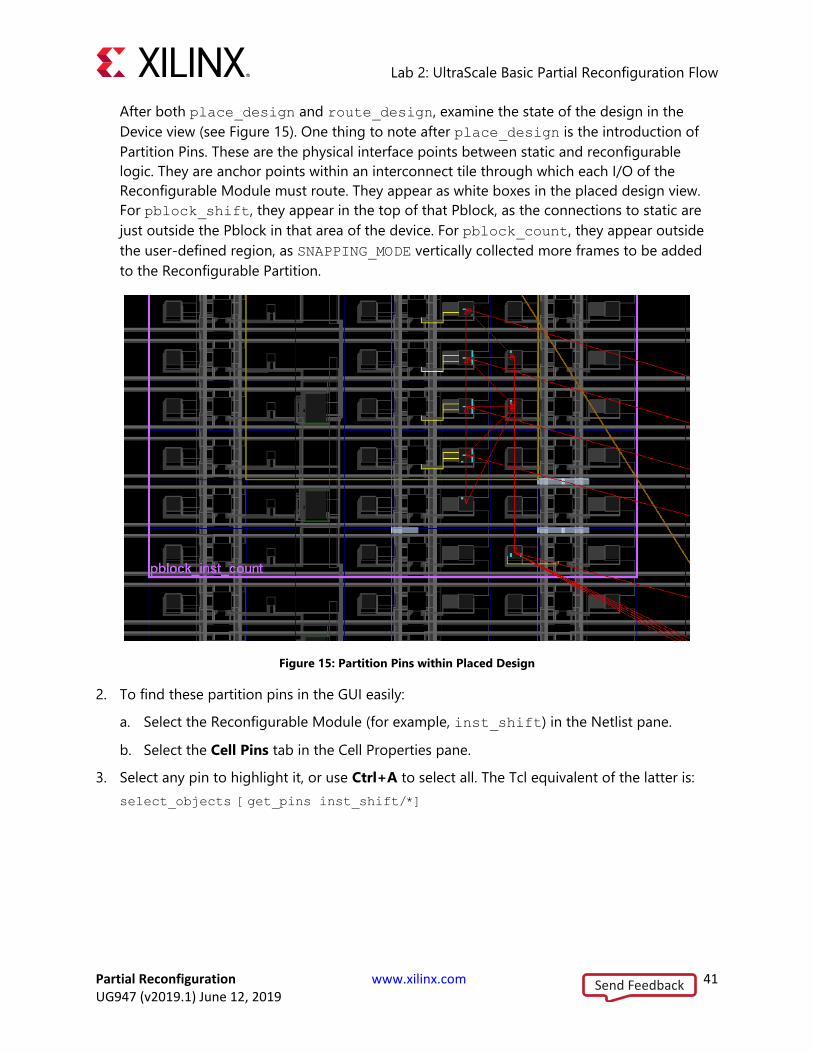
After both place_design and route_design, examine the state of the design in the
Device view (see Figure 15). One thing to note after place_design is the introduction of
Partition Pins. These are the physical interface points between static and reconfigurable
logic. They are anchor points within an interconnect tile through which each I/O of the
Reconfigurable Module must route. They appear as white boxes in the placed design view.
For pblock_shift, they appear in the top of that Pblock, as the connections to static are
just outside the Pblock in that area of the device. For pblock_count, they appear outside
the user-defined region, as SNAPPING_MODE vertically collected more frames to be added
to the Reconfigurable Partition.
Figure 15: Partition Pins within Placed Design
2. To find these partition pins in the GUI easily:
a. Select the Reconfigurable Module (for example, inst_shift) in the Netlist pane.
b. Select the Cell Pins tab in the Cell Properties pane.
3. Select any pin to highlight it, or use Ctrl+A to select all. The Tcl equivalent of the latter is:
select_objects [get_pins inst_shift/*]
Send Feedback
Lab 2: UltraScale Basic Partial Reconfiguration Flow
Partial Reconfiguration www.xilinx.com 42 UG947 (v2019.1) June 12, 2019
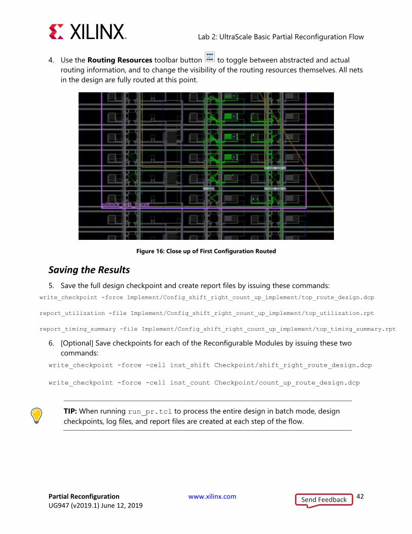
4. Use the Routing Resources toolbar button to toggle between abstracted and actual
routing information, and to change the visibility of the routing resources themselves. All nets
in the design are fully routed at this point.
Figure 16: Close up of First Configuration Routed
Saving the Results
5. Save the full design checkpoint and create report files by issuing these commands:
write_checkpoint -force Implement/Config_shift_right_count_up_implement/top_route_design.dcp
report_utilization -file Implement/Config_shift_right_count_up_implement/top_utilization.rpt
report_timing_summary -file Implement/Config_shift_right_count_up_implement/top_timing_summary.rpt
6. [Optional] Save checkpoints for each of the Reconfigurable Modules by issuing these two
commands:
write_checkpoint -force -cell inst_shift Checkpoint/shift_right_route_design.dcp
write_checkpoint -force -cell inst_count Checkpoint/count_up_route_design.dcp
TIP: When running run_pr.tcl to process the entire design in batch mode, design
checkpoints, log files, and report files are created at each step of the flow.
Send Feedback

Lab 2: UltraScale Basic Partial Reconfiguration Flow
Partial Reconfiguration www.xilinx.com 43 UG947 (v2019.1) June 12, 2019
At this point, you have created a fully implemented partial reconfiguration design from
which you can generate full and partial bitstreams. The static portion of this configuration is
used for all subsequent configurations. To isolate the static design, remove the current
Reconfigurable Modules. Make sure routing resources are enabled, and zoom in to an
interconnect tile with partition pins.
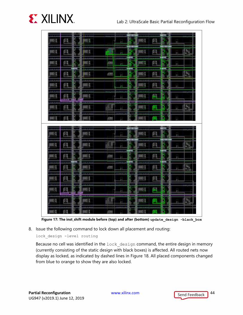
7. Clear out Reconfigurable Module logic by issuing the following commands:
update_design -cell inst_shift -black_box
update_design -cell inst_count -black_box
Issuing these commands results in many design changes as shown in Figure 17:
o The number of Fully Routed nets (green) decreased.
o inst_shift and inst_count now appear in the Netlist view as empty.
Send Feedback
Lab 2: UltraScale Basic Partial Reconfiguration Flow
Partial Reconfiguration www.xilinx.com 44 UG947 (v2019.1) June 12, 2019
Figure 17: The inst_shift module before (top) and after (bottom) update_design -black_box
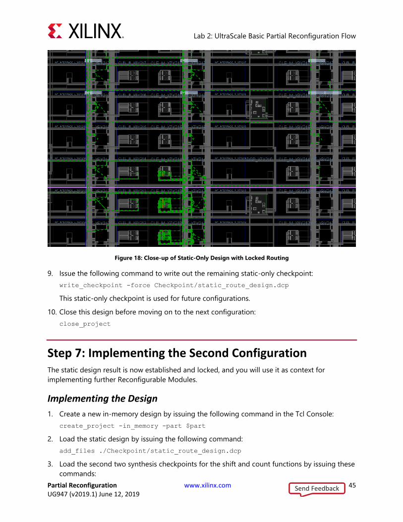
8. Issue the following command to lock down all placement and routing:
lock_design -level routing
Because no cell was identified in the lock_design command, the entire design in memory
(currently consisting of the static design with black boxes) is affected. All routed nets now
display as locked, as indicated by dashed lines in Figure 18. All placed components changed
from blue to orange to show they are also locked.
Send Feedback
Lab 2: UltraScale Basic Partial Reconfiguration Flow
Partial Reconfiguration www.xilinx.com 45 UG947 (v2019.1) June 12, 2019
Figure 18: Close-up of Static-Only Design with Locked Routing
9. Issue the following command to write out the remaining static-only checkpoint:
write_checkpoint -force Checkpoint/static_route_design.dcp
This static-only checkpoint is used for future configurations.
10. Close this design before moving on to the next configuration:
close_project
Step 7: Implementing the Second Configuration The static design result is now established and locked, and you will use it as context for
implementing further Reconfigurable Modules.
Implementing the Design
1. Create a new in-memory design by issuing the following command in the Tcl Console:
create_project -in_memory -part $part
2. Load the static design by issuing the following command:
add_files ./Checkpoint/static_route_design.dcp
3. Load the second two synthesis checkpoints for the shift and count functions by issuing these
commands:
Send Feedback
Lab 2: UltraScale Basic Partial Reconfiguration Flow
Partial Reconfiguration www.xilinx.com 46 UG947 (v2019.1) June 12, 2019
add_file ./Synth/shift_left/shift_synth.dcp
set_property SCOPED_TO_CELLS {inst_shift} [get_files ./Synth/shift_left/shift_synth.dcp]
add_file ./Synth/count_down/count_synth.dcp
set_property SCOPED_TO_CELLS {inst_count} [get_files ./Synth/count_down/count_synth.dcp]
4. Link the entire design together using the link_design command:
link_design -mode default -reconfig_partitions {inst_shift inst_count} -part $part -top top
At this point, a full configuration is loaded. This time, however, the static design is routed
and locked, and the reconfigurable logic is still just a netlist. Place and route from here only
applies to the RM logic.
5. Optimize, place and route the new RMs in the context of static by issuing these commands:
opt_design
place_design
route_design
The design is again fully implemented, now with the new Reconfigurable Module variants.
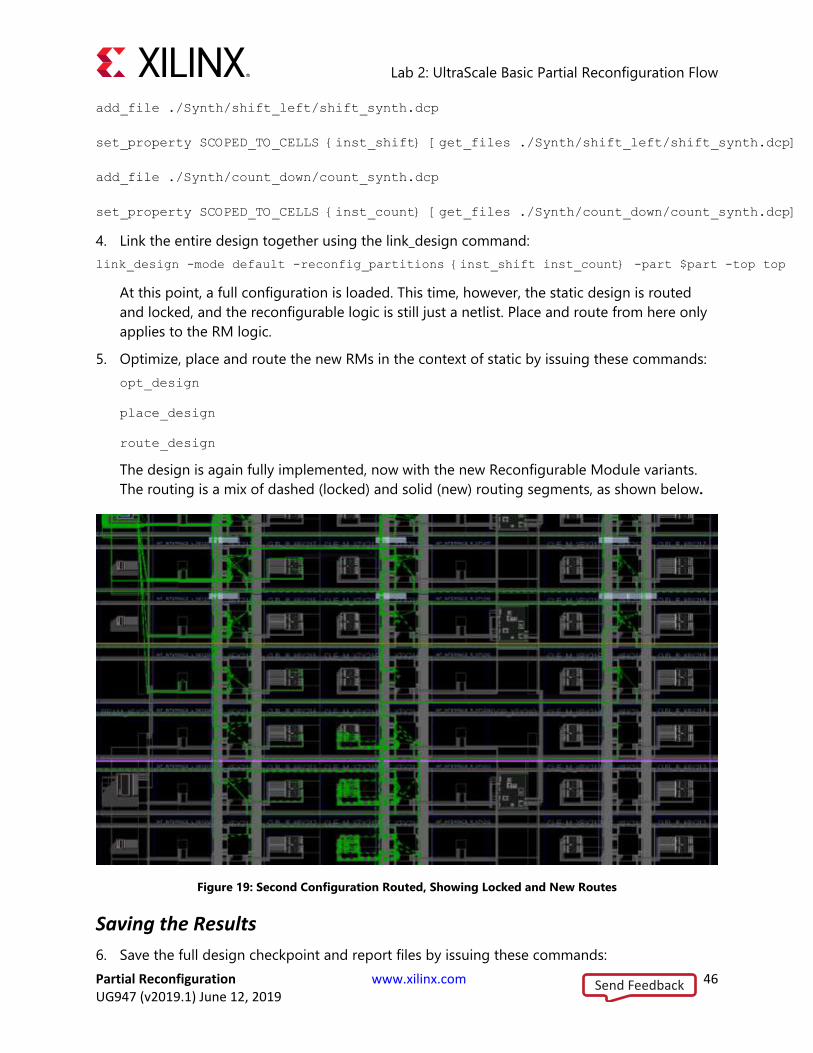
The routing is a mix of dashed (locked) and solid (new) routing segments, as shown below.
Figure 19: Second Configuration Routed, Showing Locked and New Routes
Saving the Results
6. Save the full design checkpoint and report files by issuing these commands:
Send Feedback
Lab 2: UltraScale Basic Partial Reconfiguration Flow
Partial Reconfiguration www.xilinx.com 47 UG947 (v2019.1) June 12, 2019
write_checkpoint -force Implement/Config_shift_left_count_down_import/top_route_design.dcp
report_utilization -file Implement/Config_shift_left_count_down_import/top_utilization.rpt
report_timing_summary -file Implement/Config_shift_left_count_down_import/top_timing_summary.rpt
7. [Optional] Save checkpoints for each of the Reconfigurable Modules by issuing these two
commands:
write_checkpoint -force -cell inst_shift Checkpoint/shift_left_route_design.dcp
write_checkpoint -force -cell inst_count Checkpoint/count_down_route_design.dcp
At this point, you have implemented the static design and all Reconfigurable Module
variants. This process would be repeated for designs that have more than two
Reconfigurable Modules per Reconfigurable Partition.
Step 8: Examining the Results with Highlighting Scripts With the routed configuration open in the IDE, run some visualization scripts to highlight tiles
and nets. These scripts identify the resources allocated for partial reconfiguration, and are
automatically generated. For UltraScale and UltraScale+ devices, there are different scripts to
show the range for placement versus routing for a given Pblock.
1. In the Tcl Console, issue the following commands from the <Extract_Dir> directory:
source hd_visual/pblock_inst_shift_Routing_AllTiles.tcl
highlight_objects -color green [get_selected_objects]
2. Click somewhere in the Device view to deselect the frames (or enter unselect_objects),
then issue the following commands:
source hd_visual/pblock_inst_shift_Placement_AllTiles.tcl
source hd_visual/pblock_inst_count_Placement_AllTiles.tcl
highlight_objects -color blue [get_selected_objects]
The partition frames appear highlighted in the Device view, as shown in Figure 20.
Send Feedback
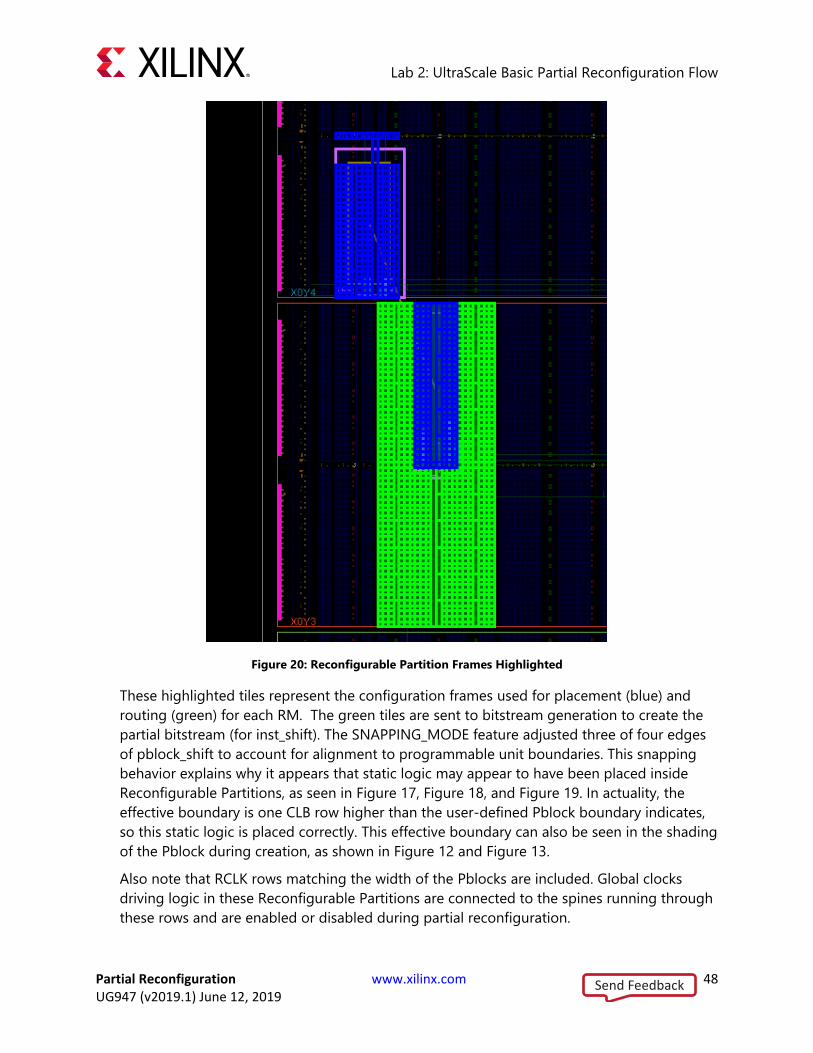
Lab 2: UltraScale Basic Partial Reconfiguration Flow
Partial Reconfiguration www.xilinx.com 48 UG947 (v2019.1) June 12, 2019
Figure 20: Reconfigurable Partition Frames Highlighted
These highlighted tiles represent the configuration frames used for placement (blue) and
routing (green) for each RM. The green tiles are sent to bitstream generation to create the
partial bitstream (for inst_shift). The SNAPPING_MODE feature adjusted three of four edges
of pblock_shift to account for alignment to programmable unit boundaries. This snapping
behavior explains why it appears that static logic may appear to have been placed inside
Reconfigurable Partitions, as seen in Figure 17, Figure 18, and Figure 19. In actuality, the
effective boundary is one CLB row higher than the user-defined Pblock boundary indicates,
so this static logic is placed correctly. This effective boundary can also be seen in the shading
of the Pblock during creation, as shown in Figure 12 and Figure 13.
Also note that RCLK rows matching the width of the Pblocks are included. Global clocks
driving logic in these Reconfigurable Partitions are connected to the spines running through
these rows and are enabled or disabled during partial reconfiguration.
Send Feedback
Lab 2: UltraScale Basic Partial Reconfiguration Flow
Partial Reconfiguration www.xilinx.com 49 UG947 (v2019.1) June 12, 2019
The other “tile” scripts are variations on these. If you had not created Pblocks that vertically
aligned to the clock region boundaries, the FrameTiles script would highlight the explicit
Pblock tiles, while the AllTiles script extends those tiles to the full reconfigurable frame
height. Note that these leave gaps where unselected frame types (for example: global clocks)
exist.
The GlitchTiles script is a subset of frame sites, avoiding dedicated silicon resources; the
other scripts are more informative than this one.
3. Close the current design:
close_project
Step 9: Generating the Bitstreams
Verifying the Configurations
RECOMMENDED: Before generating bitstreams, verify all configurations to ensure
that the static portion of each configuration match identically, so the resulting
bitstreams are safe to use in silicon. The PR Verify feature examines the complete static
design up to and including the partition pins, confirming that they are identical.
Placement and routing within the Reconfigurable Modules is not checked, as different
module results are expected here.
1. Run the pr_verify command from the Tcl Console:
pr_verify Implement/Config_shift_right_count_up_implement/top_route_design.dcp
Implement/Config_shift_left_count_down_import/top_route_design.dcp
If successful, this command returns the following message.
INFO: [Vivado 12-3253] PR_VERIFY: check points
Implement/Config_shift_right_count_up/top_route_design.dcp and
Implement/Config_shift_left_count_down/top_route_design.dcp are compatible
By default, only the first mismatch (if any) is reported. To see all mismatches, use the
-full_check option.
2. Close the project:
close_project
Generating Bitstreams
Now that the configurations have been verified, you can generate bitstreams and use them to
target your selected demonstration board.
Note: The first configuration implements shift_right and count_up. The second
configuration implements shift_left and count_down.
Send Feedback
Lab 2: UltraScale Basic Partial Reconfiguration Flow
Partial Reconfiguration www.xilinx.com 50 UG947 (v2019.1) June 12, 2019
3. First, read the first configuration into memory:
open_checkpoint Implement/Config_shift_right_count_up_implement/top_route_design.dcp
4. Generate full and partial bitstreams for this design. Be sure to keep the bit files in a unique
directory related to the full design checkpoint from which they were created.
write_bitstream -force -file Bitstreams/Config_RightUp.bit
close_project
Notice that five (or three, if you are using an UltraScale+ device) bitstreams have been
created:
o Config_RightUp.bit
This is the power-up, full design bitstream. The four shift LEDs on the right will shift
right and the four count LEDs on the left will count up.
o Config_RightUp_pblock_inst_shift_partial.bit
This is the partial bit file for the shift_right module that causes the shift LEDs to
shift right.
o Config_RightUp_pblock_inst_count_partial.bit
This is the partial bit file for the count_up module that causes the count LEDs to
count up.
o Config_RightUp_pblock_inst_shift_partial_clear.bit
This is the clearing bit file for the shift_right module for UltraScale devices only.
It safely clears a right shift to allow the shift module to be reconfigured.
o Config_RightUp_pblock_inst_count_partial_clear.bit
This is the clearing bit file for the count_up module for UltraScale devices only. It
safely clears an up count to allow the count module to be reconfigured.
IMPORTANT: When generated by a single call to write_bitstream, the names of
the bit files currently do not reflect the name of the Reconfigurable Module variant to
clarify which image is loaded. The current solution uses the base name given by the -
file option and appends the Pblock name of the reconfigurable cell. It is critical to
provide enough description in the base name to be able to identify the reconfigurable
bit files clearly. All partial bit files have the _partial postfix, and all clearing bit files
have the _partial_clear postfix.
Using run_pr.tcl to process the entire design through bitstream generation, uses a
different technique for generating the bitstreams. Opening a routed design checkpoint
issues multiple calls to write_bitstream, which gives you more control over naming
bitstreams and allows for different options (such a bitstream compression) to be applied to
full versus partial bitstreams. For example, the names configured in the run_pr.tcl script
are:
o Config_shift_right_count_up_implement_full.bit
This is the power-up, full design bitstream.
Send Feedback
Lab 2: UltraScale Basic Partial Reconfiguration Flow
Partial Reconfiguration www.xilinx.com 51 UG947 (v2019.1) June 12, 2019
o pblock_shift_shift_right_partial.bit
This is the partial bit file for the shift_right module.
o pblock_count_count_up_partial.bit
This is the partial bit file for the count_up module.
o pblock_shift_shift_right_partial_clear.bit
This is the clearing bit file for the shift_right module for UltraScale devices only.
o pblock_count_count_up_partial_clear.bit
This is the clearing bit file for the count_up module for UltraScale devices only.
5. Generate full and partial bitstreams for the second configuration, again keeping the resulting
bit files in the appropriate folder.
open_checkpoint Implement/Config_shift_left_count_down_import/top_route_design.dcp
write_bitstream -force -file Bitstreams/Config_LeftDown.bit
close_project
Similarly, five (or three) bitstreams are created, this time with a different base name.
6. Generate a full bitstream with grey boxes, plus blanking bitstreams for the Reconfigurable
Modules. Blanking bitstreams can be used to “erase” an existing configuration to reduce
power consumption.
Note: Grey box blanking bitstreams are not the same as clearing bitstreams. Clearing
bitstreams are required to prepare the global signal mask for the next partial bitstream,
ensuring the GSR event occurs properly.
open_checkpoint Checkpoint/static_route_design.dcp
update_design -cell inst_count -buffer_ports
update_design -cell inst_shift -buffer_ports
place_design
route_design
write_checkpoint -force Checkpoint/config_grey_box.dcp
write_bitstream -force -file Bitstreams/config_grey_box.bit
close_project
Send Feedback

Lab 2: UltraScale Basic Partial Reconfiguration Flow
Partial Reconfiguration www.xilinx.com 52 UG947 (v2019.1) June 12, 2019
The base configuration bitstream has no logic for either reconfigurable partition. The
update_design commands here insert constant drivers (ground) for all outputs of the
Reconfigurable Partitions, so these outputs do not float. The term grey box indicates that the
modules are not completely empty with these LUTs inserted, as opposed to black boxes,
which would have dangling nets in and out of this region. The place_design and
route_design commands ensure they are completely implemented. As valid
Reconfigurable Modules, note that these instances also have clearing bitstreams for
UltraScale devices only.
Step 10: Partially Reconfiguring the FPGA The count_shift_led design targets one of four demonstration boards. The current design
supports the KCU105, VCU108, KCU116, and VCU118 boards, revisions Rev 1.0 and newer.
Configuring the Device with a Full Image
1. Connect the board to your computer using the Platform Cable USB and power on the board.
2. From the main Vivado IDE, select Flow > Open Hardware Manager.
3. Select Open target on the green banner. Follow the steps in the wizard to establish
communication with the board.
4. Select Program device on the green banner and pick the target device, e.g. xcku040_0.
5. Navigate to the Bitstreams folder to select Config_RightUp.bit, then click OK to
program the device.
You should now see the bank of GPIO LEDs performing two tasks. Four LEDs are performing
a counting-up function (MSB is on the left), and the other four are shifting to the right. Note
the amount of time it took to configure the full device.
Partially Reconfiguring the Device
At this point, you can partially reconfigure the active device with any of the partial bitstreams
that you have created, starting first with the appropriate clearing bitstream.
6. UltraScale targets only: Select Program device on the green banner again. Navigate to the
Bitstreams folder to select
Config_RightUp_pblock_inst_shift_partial_clear.bit, then click OK to
program the device.
The shift portion of the LEDs stopped, but the counter kept counting up, unaffected by the
reconfiguration. Note the much shorter configuration time, as well as the fact that the DONE
LED turned off.
7. UltraScale targets only: Select Program device on the green banner again. Navigate to the
Bitstreams folder to select Config_LeftDown_pblock_inst_shift_partial.bit,
then click OK to program the device.
Send Feedback

Lab 2: UltraScale Basic Partial Reconfiguration Flow
Partial Reconfiguration www.xilinx.com 53 UG947 (v2019.1) June 12, 2019
The shift portion of the LEDs restarted in the opposite direction, and the DONE LED is back
on.
8. Select Program device on the green banner again. Navigate to the Bitstreams folder to
select Config_RightUp_pblock_inst_count_partial_clear.bit, then click OK to
program the device.
The count portion of the LEDs stopped, but the shifter kept shifting, unaffected by the
reconfiguration.
9. Select Program device on the green banner again. Navigate to the Bitstreams folder to
select Config_LeftDown_pblock_inst_count_partial.bit, then click OK to
program the device.
The counter is now counting down, and the shifting LEDs were unaffected by the
reconfiguration. This process can be repeated with the Config_RightUp partial bit files to
return to the original configuration, or with the blanking partial bit files to stop activity on
the LEDs (they will stay on). Keep track of the currently loaded module for each partition to
ensure the correct clearing bitstream is loaded before the next partial bitstream.
Conclusion This concludes Lab 2. In this lab, you:
• Synthesized a design bottom-up to prepare for partial reconfiguration implementation
• Created a valid floorplan for a partial reconfiguration design
• Created two configurations with common static results
• Implemented these two configurations, saving the static design to be used in each
• Created checkpoints for static and reconfigurable modules for later reuse
• Examined framesets and verified the two configurations
• Created full, partial, and clearing bitstreams
• Configured and partially reconfigured an FPGA
Send Feedback
Partial Reconfiguration www.xilinx.com 54 UG947 (v2019.1) June 12, 2019
Lab 3: Partial Reconfiguration Project Flow
Overview In this lab, you will create a new project and set up all the sources and runs defining the
structure of a PR design. The design used in this lab is based on the simple design in labs 1 and
2, but modified so it has two instances of the shift module instead of one shift and one count.
This shows the implications of Partition Definitions in the project flow.
This lab currently targets the following Xilinx® development platforms:
• KC705 (Kintex™-7)
• VC707 (Virtex™-7)
• VC709 (Virtex-7)
• KCU105 (Kintex UltraScale™)
• VCU108 (Virtex UltraScale)
• KCU116 (Kintex UltraScale+™)
• VCU118 (Virtex UltraScale+)
Step 1: Extracting the Tutorial Design Files 1. To obtain the tutorial design file, see Tutorial Design Description.
2. Navigate to \pr_project in the extracted files. The pr_project data directory is referred
to in this lab as the <Extract_Dir>.
Step 2: Loading Initial Design Sources The first unique step in any PR design flow (project based or otherwise) is to define the parts of
the design that will be marked reconfigurable. This is done via context menus in the
Hierarchical Source View in project mode. These steps will walk through initial project creation
through definition of partitions in a simple design.
1. Extract the design from the archive. The pr_project data directory is referred to in this
tutorial as the <Extract_Dir>.
2. Open the Vivado IDE and select Create Project, then click Next.
Send Feedback

Lab 3: Partial Reconfiguration Project Flow
Partial Reconfiguration www.xilinx.com 55 UG947 (v2019.1) June 12, 2019
3. Select the <Extract_Dir> as the Project location. Leave the Project name as
project_1, and leave the Create project subdirectory option checked. Click Next.
4. Select RTL Project and ensure the Do not specify sources checkbox is unchecked, then
click Next.
5. Click the Add Directories button and select these Sources directories to be added to the
design:
o <Extract_Dir>\Sources\hdl\top
o <Extract_Dir>\Sources\hdl\shift_right
6. Click Next to get to the Add Constraints window, then select these files:
o <Extract_Dir>\Sources\xdc\top_io_<board>.xdc
o <Extract_Dir>\Sources\xdc\pblocks_<board>.xdc
Note that these constraint files are full design constraints, scoped to the top level design. If
you would like to perform your own floorplanning, only select the top_io xdc, omitting the
pblocks xdc. Stop the flow after synthesis to create your own floorplan.
7. Click Next to choose the part. In the Part selector, click on Boards and choose the target
board matching the constraint file(s) you have selected. Then click Next and then Finish to
complete project creation. The Sources window shows a standard hierarchical view of the
design.
Figure 21: Sources View After Project Creation
At this point, a standard project is open. Nothing specific to Partial Reconfiguration has been
done.
8. Select Tools > Enable Partial Reconfiguration
Send Feedback

Lab 3: Partial Reconfiguration Project Flow
Partial Reconfiguration www.xilinx.com 56 UG947 (v2019.1) June 12, 2019
This prepares the project for the PR design flow. Once this is set it cannot be undone, so
archive your project before selecting this option.
Figure 22: Enabling Partial Reconfiguration
In the ensuing dialog box, click Convert to turn this project into a PR project.
9. Right-click on one of the “shift” instances and select the Create Partition Definition…
option.
This action will define *both* shift instances as Reconfigurable Partitions in the design. Since
each instance has come from the same RTL source, they are logically identical. Out-of-
context synthesis will be run to keep this module separated from top, and the one post-
synthesis checkpoint will be used for both shift instances.
TIP: If there are multiple instantiations of the same module within a design, but not all
need to be reconfigurable, then the modules must be manually modified to become
unique. Then you can independently tag desired instances as Reconfigurable Partitions.
10. In the dialog box that appears, give names to both the Partition Definition and the
Reconfigurable Module. The Partition Definition is the general reference for the workspace
into which all Reconfigurable Modules will be inserted, so give it an appropriate name, such
as shifter. The Reconfigurable Module refers to this specific RTL instance, so give it a
name that references its functionality, such as shift_right, then click OK.
Send Feedback
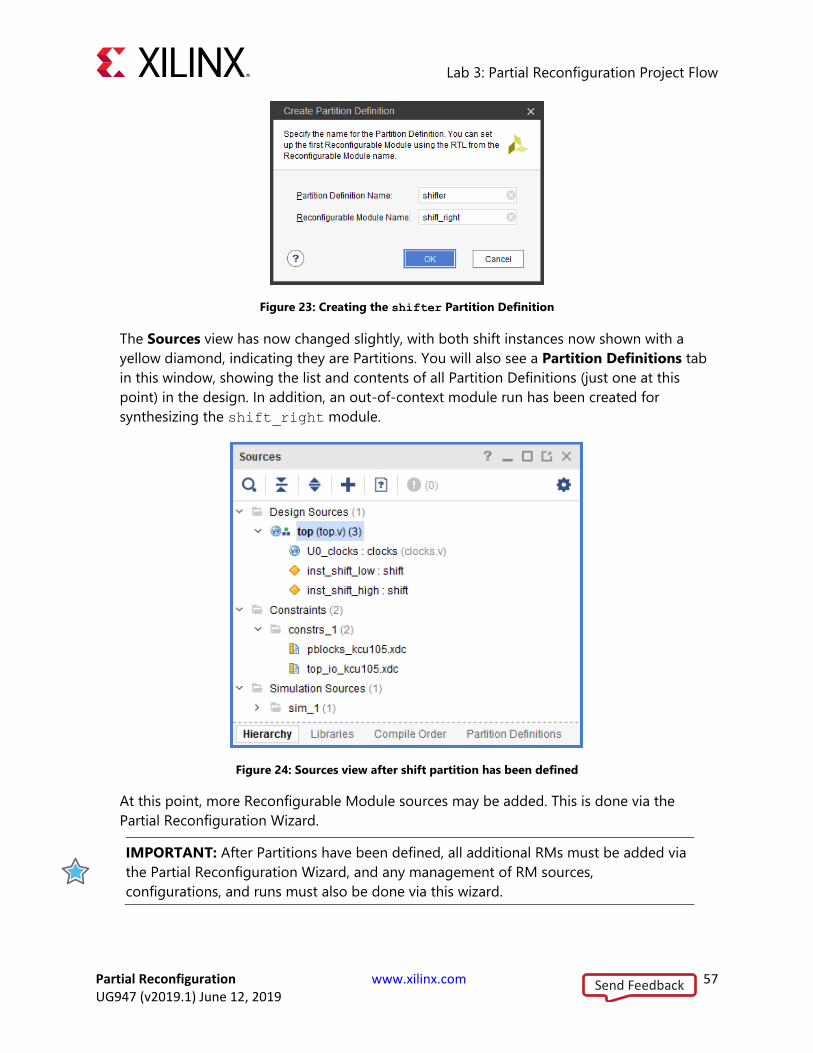
Lab 3: Partial Reconfiguration Project Flow
Partial Reconfiguration www.xilinx.com 57 UG947 (v2019.1) June 12, 2019
Figure 23: Creating the shifter Partition Definition
The Sources view has now changed slightly, with both shift instances now shown with a
yellow diamond, indicating they are Partitions. You will also see a Partition Definitions tab
in this window, showing the list and contents of all Partition Definitions (just one at this
point) in the design. In addition, an out-of-context module run has been created for
synthesizing the shift_right module.
Figure 24: Sources view after shift partition has been defined
At this point, more Reconfigurable Module sources may be added. This is done via the
Partial Reconfiguration Wizard.
IMPORTANT: After Partitions have been defined, all additional RMs must be added via
the Partial Reconfiguration Wizard, and any management of RM sources,
configurations, and runs must also be done via this wizard.
Send Feedback

Lab 3: Partial Reconfiguration Project Flow
Partial Reconfiguration www.xilinx.com 58 UG947 (v2019.1) June 12, 2019
Step 3: Completing the Design with the Partial Reconfiguration Wizard 1. Launch the Partial Reconfiguration Wizard by selecting this option under the Tools menu
or from the Flow Navigator.
2. Click Next to get to the Edit Reconfigurable Modules page. Here you can see the
shift_right RM already exists, and there are add, remove and edit buttons on the left hand
side of the window, above the RMs. Click on the blue + icon to add a new RM.
3. Click the Add Directories button to select the shift_left folder:
<Extract_Dir>\Sources\hdl\shift_left
Or use the Add Files button to select the shift_left.v file residing in this directory. If module-
level constraints were needed, they would be added here. Note that they would need to be
scoped to the level of hierarchy for this Partition.
Fill in the Reconfigurable Module field to be shift_left. Set the Partition Definition to be
shifter, leave Top Module field empty and the Sources are already synthesized check
box unchecked. Click OK to create the new module.
Two Reconfigurable Modules are now available for the shifter Reconfigurable Partition.
Figure 25: Partial Reconfiguration Wizard with two Reconfigurable Modules defined
On the next page, Configurations are defined. Configurations are full design images
consisting of the static design and one RM per RP. You can either create any desired set of
configurations, or simply let the wizard select them for you.
Send Feedback

Lab 3: Partial Reconfiguration Project Flow
Partial Reconfiguration www.xilinx.com 59 UG947 (v2019.1) June 12, 2019
4. Let the Wizard create the configurations by selecting the automatically create
configurations link.
Figure 26: Partial Reconfiguration Wizard Configurations page
After selecting this option, the minimum set of two configurations has been created. Each
shift instance has been given shift_right in the first configuration and shift_left in the
second configuration. Note that the Configuration Name is editable – in the example
below, the names have been updated to config_right and config_left to reflect the
Reconfigurable Modules contained within each one.
Send Feedback
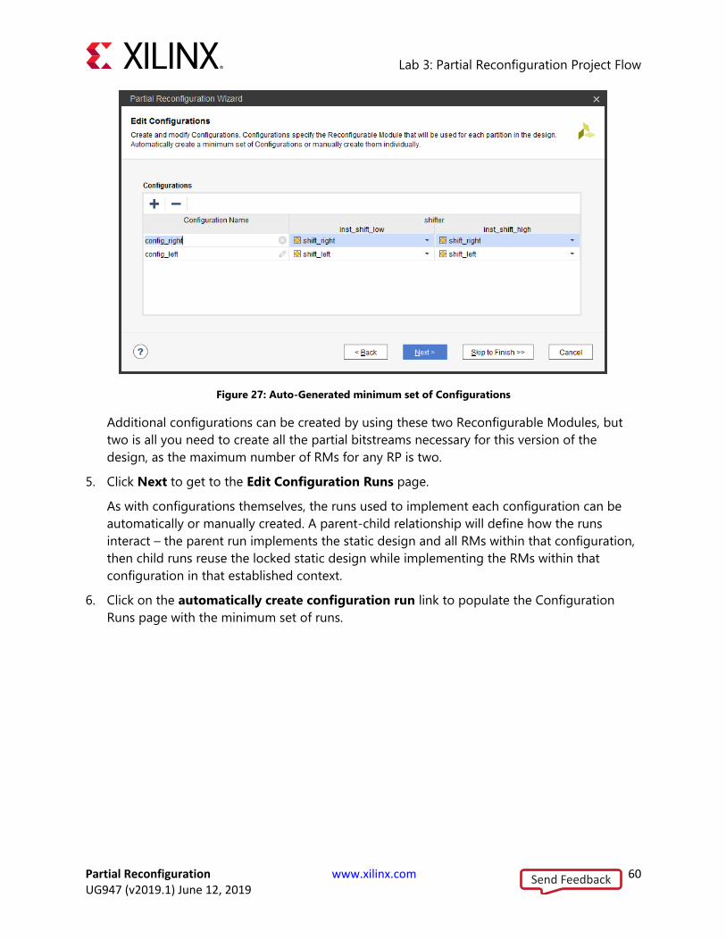
Lab 3: Partial Reconfiguration Project Flow
Partial Reconfiguration www.xilinx.com 60 UG947 (v2019.1) June 12, 2019
Figure 27: Auto-Generated minimum set of Configurations
Additional configurations can be created by using these two Reconfigurable Modules, but
two is all you need to create all the partial bitstreams necessary for this version of the
design, as the maximum number of RMs for any RP is two.
5. Click Next to get to the Edit Configuration Runs page.
As with configurations themselves, the runs used to implement each configuration can be
automatically or manually created. A parent-child relationship will define how the runs
interact – the parent run implements the static design and all RMs within that configuration,
then child runs reuse the locked static design while implementing the RMs within that
configuration in that established context.
6. Click on the automatically create configuration run link to populate the Configuration
Runs page with the minimum set of runs.
Send Feedback
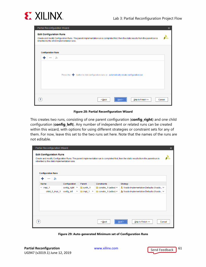
Lab 3: Partial Reconfiguration Project Flow
Partial Reconfiguration www.xilinx.com 61 UG947 (v2019.1) June 12, 2019
Figure 28: Partial Reconfiguration Wizard
This creates two runs, consisting of one parent configuration (config_right) and one child
configuration (config_left). Any number of independent or related runs can be created
within this wizard, with options for using different strategies or constraint sets for any of
them. For now, leave this set to the two runs set here. Note that the names of the runs are
not editable.
Figure 29: Auto-generated Minimum set of Configuration Runs
Send Feedback

Lab 3: Partial Reconfiguration Project Flow
Partial Reconfiguration www.xilinx.com 62 UG947 (v2019.1) June 12, 2019
7. Click Next to see the Summary page then Finish to complete the design setup and exit the
Wizard.
IMPORTANT: Nothing is created or modified until you click Finish to exit the Partial
Reconfiguration Wizard. All actions are queued until this last click, so it is possible to
step forward and back as needed without implementing changes until you are ready.
Back in the Vivado IDE, you will see that the Design Runs window has been updated. A
second out-of-context synthesis run has been added for the shift_left RM, and a child
implementation run (child_0_impl_1) has been created under the parent (impl_1). You are
now ready to process the design.
Figure 30: Design Runs window showing all synthesis and implementation ready to launch
Step 4: Synthesizing and Implementing the Current Design With the design from above open in the Vivado IDE, take a look at the Design Runs window.
The top-level design synthesis run (synth_1) and the parent implementation run (impl_1) are
marked “active.” The Flow Navigator actions apply to these active runs and their child runs, so
clicking on Run Synthesis or Run Implementation pulls the design through only these runs, as
well as the OOC synthesis runs needed to complete them. You can select a specific parent or
child implementation run, right-click and select Launch Runs to pull through the entire flow for
that ultimate target.
1. In the Flow Navigator, click Run Synthesis. When synthesis completes, select Open
Synthesized Design.
This action will synthesize all OOC modules, followed by synthesis of the top level design.
This is no different than any design with OOC modules (IP or otherwise).
In the post-synthesis design that opens, note that two Pblocks have already been defined.
These were supplied in pblocks_<board>.xdc and map to the two shift instances in top.
If no Pblocks had existed with the design sources, they could be created at this step in the
Send Feedback

Lab 3: Partial Reconfiguration Project Flow
Partial Reconfiguration www.xilinx.com 63 UG947 (v2019.1) June 12, 2019
flow. This can be done by right-clicking on an inst_shift instance in the design hierarchy to
select Floorplanning > Draw Pblock. Each instance will require its own unique Pblock.
Figure 31: Floorplan with two Reconfigurable Partitions (KC105 shown)
2. Select one of the two Pblocks in the floorplan and note its properties. The last two
properties listed are RESET_AFTER_RECONFIG (7 series only) and SNAPPING_MODE, two
properties specific to Partial Reconfiguration. Note that both of these options have been
enabled in the Pblocks xdc.
3. Run PR-specific design rule checks by selecting Reports > Report DRC. To save time, you
can deselect all checkboxes other than the one for Partial Reconfiguration.
Send Feedback
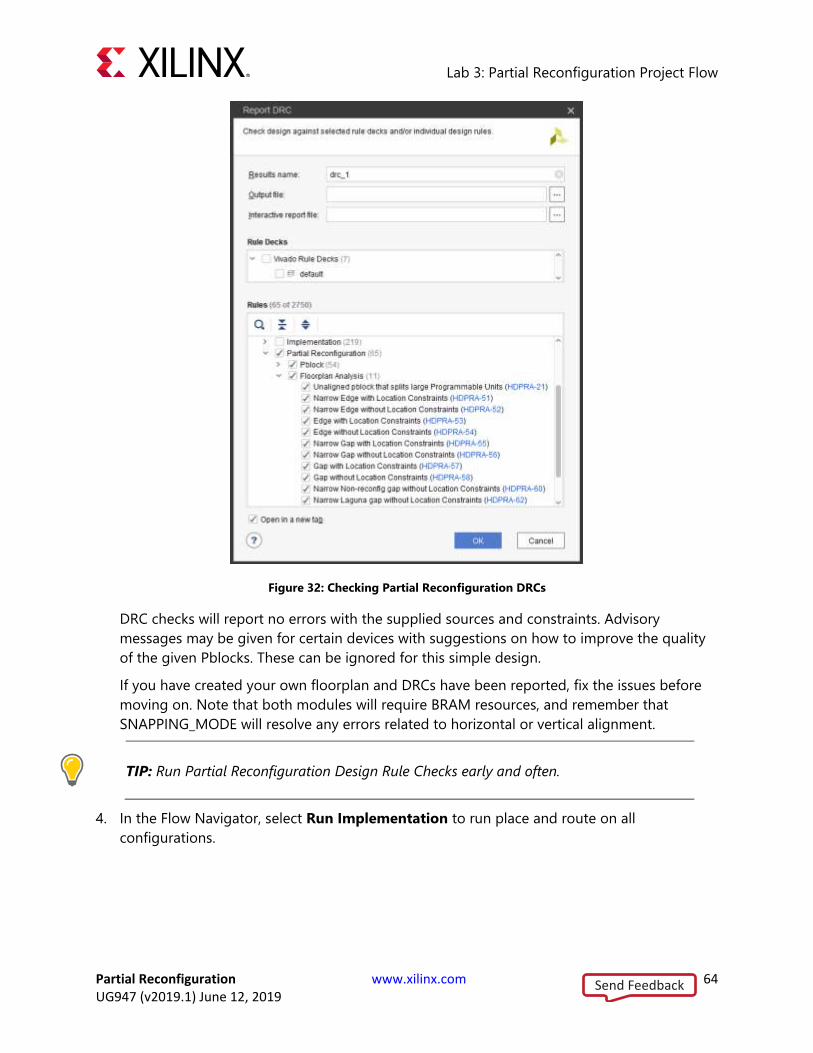
Lab 3: Partial Reconfiguration Project Flow
Partial Reconfiguration www.xilinx.com 64 UG947 (v2019.1) June 12, 2019
Figure 32: Checking Partial Reconfiguration DRCs
DRC checks will report no errors with the supplied sources and constraints. Advisory
messages may be given for certain devices with suggestions on how to improve the quality
of the given Pblocks. These can be ignored for this simple design.
If you have created your own floorplan and DRCs have been reported, fix the issues before
moving on. Note that both modules will require BRAM resources, and remember that
SNAPPING_MODE will resolve any errors related to horizontal or vertical alignment.
TIP: Run Partial Reconfiguration Design Rule Checks early and often.
4. In the Flow Navigator, select Run Implementation to run place and route on all
configurations.
Send Feedback
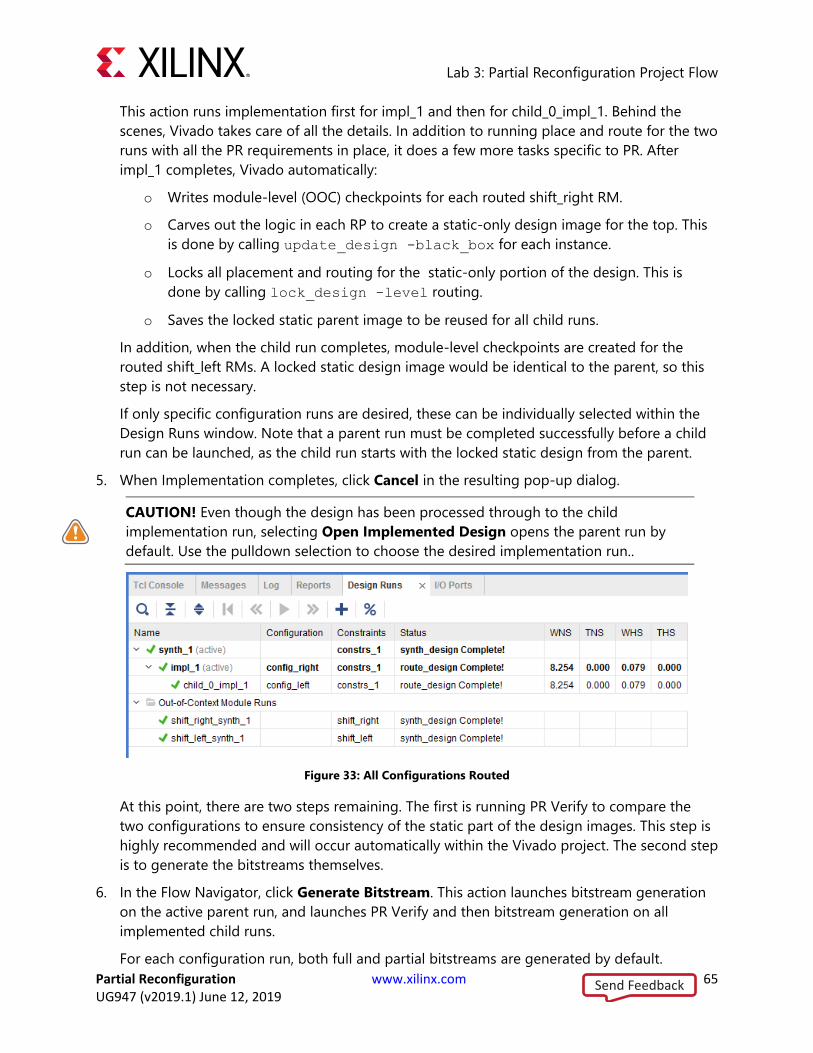
Lab 3: Partial Reconfiguration Project Flow
Partial Reconfiguration www.xilinx.com 65 UG947 (v2019.1) June 12, 2019
This action runs implementation first for impl_1 and then for child_0_impl_1. Behind the
scenes, Vivado takes care of all the details. In addition to running place and route for the two
runs with all the PR requirements in place, it does a few more tasks specific to PR. After
impl_1 completes, Vivado automatically:
o Writes module-level (OOC) checkpoints for each routed shift_right RM.
o Carves out the logic in each RP to create a static-only design image for the top. This
is done by calling update_design -black_box for each instance.
o Locks all placement and routing for the static-only portion of the design. This is
done by calling lock_design -level routing.
o Saves the locked static parent image to be reused for all child runs.
In addition, when the child run completes, module-level checkpoints are created for the
routed shift_left RMs. A locked static design image would be identical to the parent, so this
step is not necessary.
If only specific configuration runs are desired, these can be individually selected within the
Design Runs window. Note that a parent run must be completed successfully before a child
run can be launched, as the child run starts with the locked static design from the parent.
5. When Implementation completes, click Cancel in the resulting pop-up dialog.
CAUTION! Even though the design has been processed through to the child
implementation run, selecting Open Implemented Design opens the parent run by
default. Use the pulldown selection to choose the desired implementation run..
Figure 33: All Configurations Routed
At this point, there are two steps remaining. The first is running PR Verify to compare the
two configurations to ensure consistency of the static part of the design images. This step is
highly recommended and will occur automatically within the Vivado project. The second step
is to generate the bitstreams themselves.
6. In the Flow Navigator, click Generate Bitstream. This action launches bitstream generation
on the active parent run, and launches PR Verify and then bitstream generation on all
implemented child runs.
For each configuration run, both full and partial bitstreams are generated by default.
Send Feedback

Lab 3: Partial Reconfiguration Project Flow
Partial Reconfiguration www.xilinx.com 66 UG947 (v2019.1) June 12, 2019
The entire Partial Reconfiguration flow can now be run in a project environment. All steps, from
module-level synthesis to bitstream generation can be done without leaving the GUI.
Step 5: Adding an Additional Reconfigurable Module and Corresponding Configuration 1. With the design open in the Vivado IDE, open the Partial Reconfiguration Wizard.
2. On the Edit Reconfigurable Modules page, click the + button to add a new RM.
3. Select the shift_right_slow.v file in <Extract_Dir>\Sources\hdl\shift_right_slow then
click OK.
4. Enter shift_right_slow for the Reconfigurable Module name and then click OK and
Next.
Figure 34: Adding a new RM shift_right_slow
Note that on the Edit Configurations page, there is no longer an option to automatically
create configurations, as you already have two existing ones. You can re-enable this option
by removing all existing configurations, but this will recreate all configurations and remove
all existing results.
5. Create a new configuration by clicking the + button, entering the name config_right_slow,
then hitting ENTER. Select shift_right_slow for each Reconfigurable Partition instance.
Send Feedback
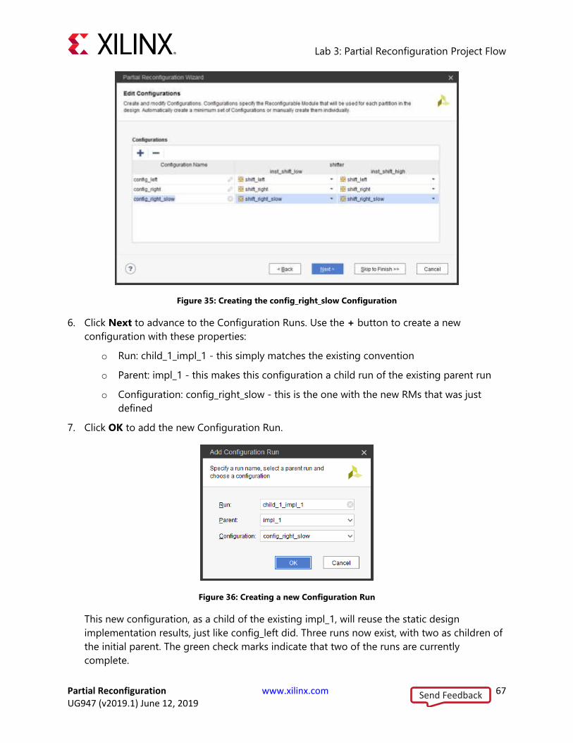
Lab 3: Partial Reconfiguration Project Flow
Partial Reconfiguration www.xilinx.com 67 UG947 (v2019.1) June 12, 2019
Figure 35: Creating the config_right_slow Configuration
6. Click Next to advance to the Configuration Runs. Use the + button to create a new
configuration with these properties:
o Run: child_1_impl_1 - this simply matches the existing convention
o Parent: impl_1 - this makes this configuration a child run of the existing parent run
o Configuration: config_right_slow - this is the one with the new RMs that was just
defined
7. Click OK to add the new Configuration Run.
Figure 36: Creating a new Configuration Run
This new configuration, as a child of the existing impl_1, will reuse the static design
implementation results, just like config_left did. Three runs now exist, with two as children of
the initial parent. The green check marks indicate that two of the runs are currently
complete.
Send Feedback
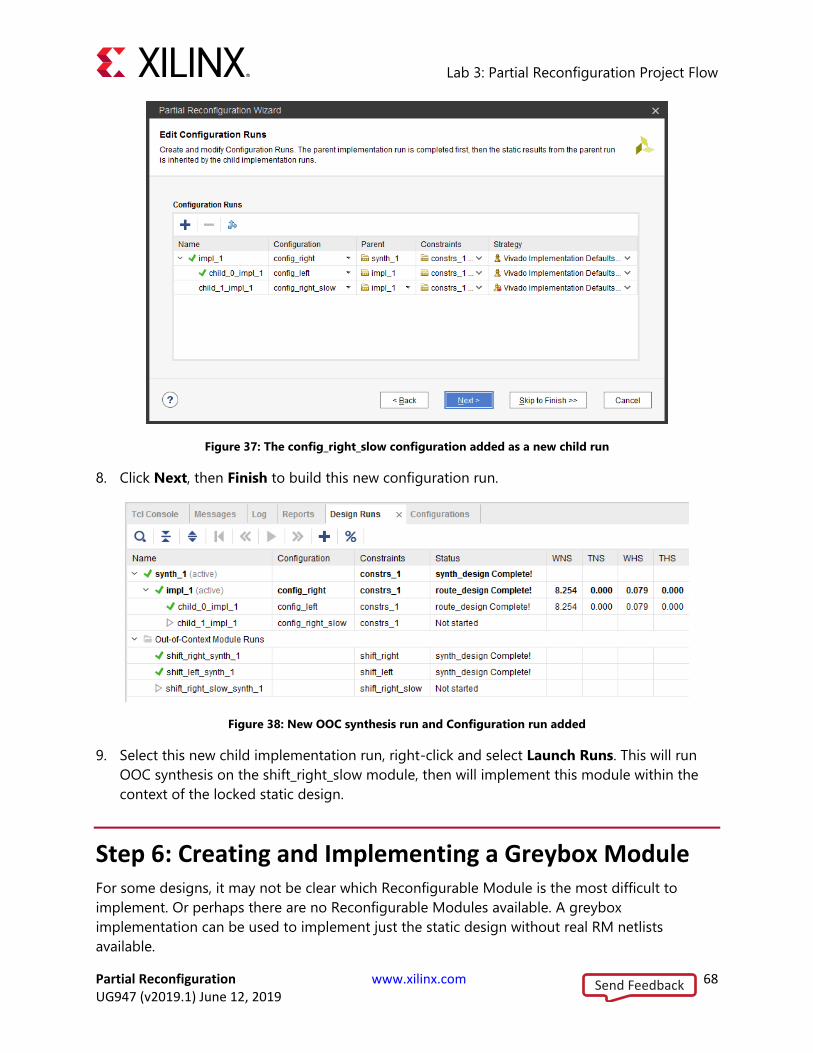
Lab 3: Partial Reconfiguration Project Flow
Partial Reconfiguration www.xilinx.com 68 UG947 (v2019.1) June 12, 2019
Figure 37: The config_right_slow configuration added as a new child run
8. Click Next, then Finish to build this new configuration run.
Figure 38: New OOC synthesis run and Configuration run added
9. Select this new child implementation run, right-click and select Launch Runs. This will run
OOC synthesis on the shift_right_slow module, then will implement this module within the
context of the locked static design.
Step 6: Creating and Implementing a Greybox Module For some designs, it may not be clear which Reconfigurable Module is the most difficult to
implement. Or perhaps there are no Reconfigurable Modules available. A greybox
implementation can be used to implement just the static design without real RM netlists
available.
Send Feedback
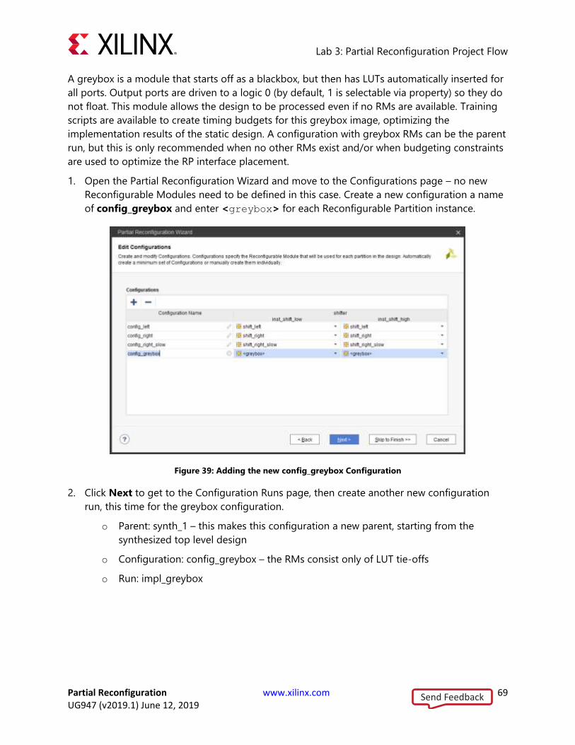
Lab 3: Partial Reconfiguration Project Flow
Partial Reconfiguration www.xilinx.com 69 UG947 (v2019.1) June 12, 2019
A greybox is a module that starts off as a blackbox, but then has LUTs automatically inserted for
all ports. Output ports are driven to a logic 0 (by default, 1 is selectable via property) so they do
not float. This module allows the design to be processed even if no RMs are available. Training
scripts are available to create timing budgets for this greybox image, optimizing the
implementation results of the static design. A configuration with greybox RMs can be the parent
run, but this is only recommended when no other RMs exist and/or when budgeting constraints
are used to optimize the RP interface placement.
1. Open the Partial Reconfiguration Wizard and move to the Configurations page – no new
Reconfigurable Modules need to be defined in this case. Create a new configuration a name
of config_greybox and enter <greybox> for each Reconfigurable Partition instance.
Figure 39: Adding the new config_greybox Configuration
2. Click Next to get to the Configuration Runs page, then create another new configuration
run, this time for the greybox configuration.
o Parent: synth_1 – this makes this configuration a new parent, starting from the
synthesized top level design
o Configuration: config_greybox – the RMs consist only of LUT tie-offs
o Run: impl_greybox
Send Feedback
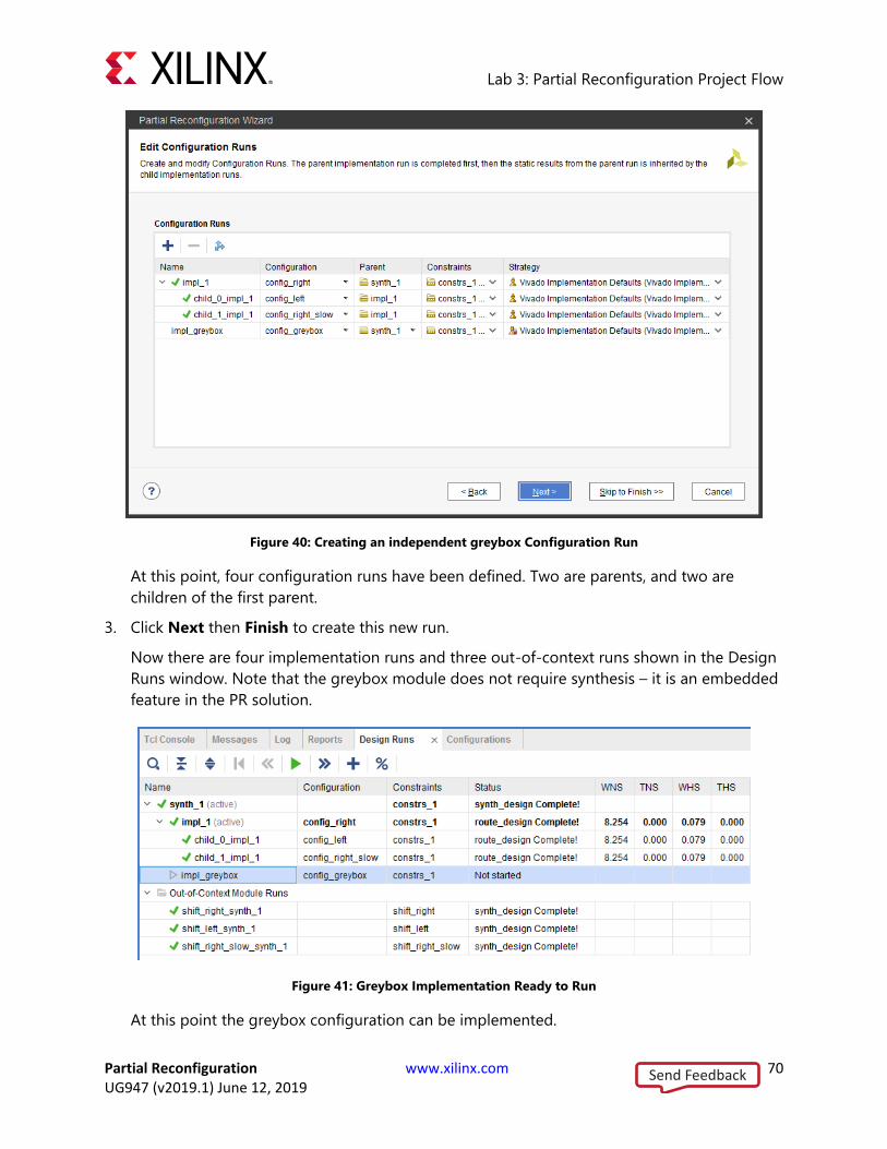
Lab 3: Partial Reconfiguration Project Flow
Partial Reconfiguration www.xilinx.com 70 UG947 (v2019.1) June 12, 2019
Figure 40: Creating an independent greybox Configuration Run
At this point, four configuration runs have been defined. Two are parents, and two are
children of the first parent.
3. Click Next then Finish to create this new run.
Now there are four implementation runs and three out-of-context runs shown in the Design
Runs window. Note that the greybox module does not require synthesis – it is an embedded
feature in the PR solution.
Figure 41: Greybox Implementation Ready to Run
At this point the greybox configuration can be implemented.
Send Feedback

Lab 3: Partial Reconfiguration Project Flow
Partial Reconfiguration www.xilinx.com 71 UG947 (v2019.1) June 12, 2019
4. Select the impl_greybox design run, right-click and select Launch Runs. The Flow Navigator
will not launch this run as it is not the active parent.
IMPORTANT: Because impl_1 and impl_greybox are both parents, their static design
results will be different, and their resulting bitstreams will NOT be compatible in
hardware. Only bitstreams derived from a single parent (and subsequently confirmed
using PR Verify) should ever be delivered via PR to a device.
Step 6: Modifying a Design Source or Options The Vivado IDE tracks dependencies between design runs. This is a critical feature for Partial
Reconfiguration given the interdependencies of configurations. If any aspect of the parent
configuration or implementation results are modified, it and all children must be recompiled.
1. Select the impl_1 design run.
2. In the Options tab of the Run Properties window, change the Strategy to
Performance_Explore.
A pop-up dialog will alert you to the fact that impl_1 will be forced out of date if you
proceed.
Figure 42: Modifying a Completed Run
3. Click Yes.
Multiple runs are now marked out-of-date: impl_1 and both child runs that depend on it.
The resulting files still exist in their respective folders, but will be deleted as soon as the
parent run is launched. The impl_greybox design run, on the other hand, remains completed
as it does not depend on impl_1 as a parent.
Note that the Strategy option for each of the child runs remains at Vivado Implementation
Defaults; child runs do not inherit options from the parent run. However, any strategy or
option in child runs will only have an effect on the Reconfigurable Module implementation,
as the static design is already routed and locked.
Send Feedback
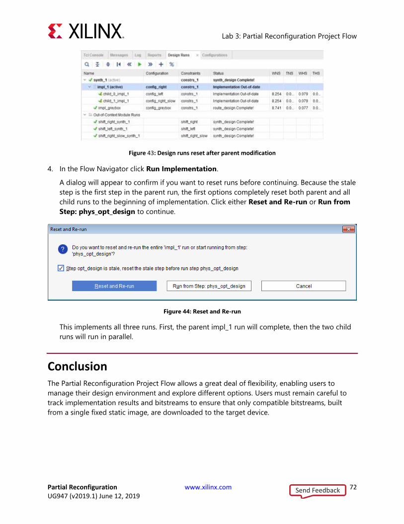
Lab 3: Partial Reconfiguration Project Flow
Partial Reconfiguration www.xilinx.com 72 UG947 (v2019.1) June 12, 2019
Figure 43: Design runs reset after parent modification
4. In the Flow Navigator click Run Implementation.
A dialog will appear to confirm if you want to reset runs before continuing. Because the stale
step is the first step in the parent run, the first options completely reset both parent and all
child runs to the beginning of implementation. Click either Reset and Re-run or Run from
Step: phys_opt_design to continue.
Figure 44: Reset and Re-run
This implements all three runs. First, the parent impl_1 run will complete, then the two child
runs will run in parallel.
Conclusion The Partial Reconfiguration Project Flow allows a great deal of flexibility, enabling users to
manage their design environment and explore different options. Users must remain careful to
track implementation results and bitstreams to ensure that only compatible bitstreams, built
from a single fixed static image, are downloaded to the target device.
Send Feedback

Partial Reconfiguration www.xilinx.com 73 UG947 (v2019.1) June 12, 2019
Lab 4: Vivado Debug and the PR Project Flow
Overview This lab covers more project-based features for the Partial Reconfiguration (PR) solution. The
following topics are covered in this lab:
• The Partial Reconfiguration project flow in the Vivado® IDE
• Current IP support within Reconfigurable Modules (RM)
• Inserting Vivado Debug cores within Reconfigurable Modules
• Improvements to reporting unique to Partial Reconfiguration
• Debugging within the Vivado Hardware Manager
It differs from the PR flow in Lab 3 in that while this Project Flow does not show greybox
implementation and a few other features, it covers IP and debugging. This lab supports the
following development platforms:
• KCU105 (Kintex™ UltraScale™)
• VCU108 (Virtex™ UltraScale)
• KCU116 (Kintex UltraScale+™)
• VCU118 (Virtex UltraScale+)
Step 1: Loading Initial Design Sources The first unique step in any PR design flow (project based or otherwise) is to define the parts of
the design to be marked as reconfigurable. This is done via context menus in the Hierarchical
Source View in project mode.
1. Extract the design from the TSC archive. The pr_project_debug data directory is referred
to in this tutorial as the <Extract_Dir>.
2. Open the Vivado IDE and select Create Project, then click Next.
3. Select the <Extract_Dir> as the Project location. Leave the Project name as
project_1, and leave the Create project subdirectory option checked. ClickNext.
4. Select RTL Project and ensure the Do not specify sources checkbox is unchecked, then
click Next.
Send Feedback

Lab 4: Vivado Debug and the PR Project Flow
Partial Reconfiguration www.xilinx.com 74 UG947 (v2019.1) June 12, 2019
5. Click the Add Files button and select these sources to add to the design:
o <Extract_Dir>\Sources\hdl\top.v
o <Extract_Dir>\Sources\hdl\multiplier\mult.v
o <Extract_Dir>\Sources\ip\<board>\clk_wiz\clk_wiz_0.xci
o <Extract_Dir>\Sources\ip\<board>\vio\vio_0.xci
Do not select add.v or mult_no_ila.v (in the adder and multiplier_without_ila
folders, respectively), as these are the sources for RMs that will be added later.
6. Select the Copy sources into project checkbox.
7. Click Next to get to the Add Constraints window, then select the following file: <Extract_Dir>\Sources\xdc\top_io_<board>.xdc
8. Select the Copy constraints files into project checkbox.
Note: These constraint files are full design constraints, scoped to the top level design. This
constraint file does not include a floorplan.
9. Click Next to choose the part. In the Part selector, click on Boards and (using filters if
needed) choose the appropriate target platform:
o Kintex UltraScale KCU105 Evaluation Platform
o Virtex UltraScale VCU108 Evaluation Platform
o Kintex UltraScale+ KCU116 Evaluation Platform
o Virtex UltraScale+ VCU118 Evaluation Platform
10. Then click Next and then Finish to complete project creation. The Sources window shows a
standard hierarchical view of the design.
Figure 45: Sources view after project creation
Send Feedback
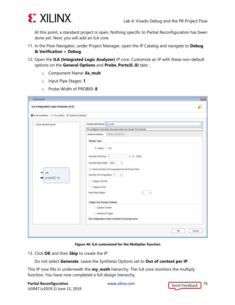
Lab 4: Vivado Debug and the PR Project Flow
Partial Reconfiguration www.xilinx.com 75 UG947 (v2019.1) June 12, 2019
At this point, a standard project is open. Nothing specific to Partial Reconfiguration has been
done yet. Next, you will add an ILA core.
11. In the Flow Navigator, under Project Manager, open the IP Catalog and navigate to Debug
& Verification > Debug.
12. Open the ILA (Integrated Logic Analyzer) IP core. Customize an IP with these non-default
options on the General Options and Probe_Ports(0..0) tabs :
o Component Name: ila_mult
o Input Pipe Stages: 1
o Probe Width of PROBE0: 8
Figure 46: ILA customized for the Multiplier function
13. Click OK and then Skip to create the IP.
Do not select Generate. Leave the Synthesis Options set to Out of context per IP.
This IP now fills in underneath the my_math hierarchy. The ILA core monitors the multiply
function. You have now completed a full design hierarchy.
Send Feedback

Lab 4: Vivado Debug and the PR Project Flow
Partial Reconfiguration www.xilinx.com 76 UG947 (v2019.1) June 12, 2019
Step 2: Setting Up the Design for Partial Reconfiguration 1. Select Tools > Enable Partial Reconfiguration
This prepares the project for the PR design flow. Once this is set it cannot be undone, so
Xilinx recommends archiving your project before selecting this option.
Figure 47: Enabling Partial Reconfiguration
In the ensuing dialog box, click Convert to turn this project into a PR project.
2. Right-click on the my_math instance in the sources window and select the Create Partition
Definition… option.
This defines this instance as a Reconfigurable Partition in the design. Out-of-context
synthesis is run to keep this module separated from top, and the post-synthesis checkpoint
is used for the math_rp instance..
TIP: If there are multiple instantiations of a module within a design, each are marked
as reconfigurable. If they all do not need to be reconfigurable, then the modules must
be manually modified to remain unique. Then you can independently tag desired
instances as Reconfigurable Partitions.
Note: Starting in Vivado 2018.3, IP placed within Reconfigurable Modules can be
synthesized as Global or Out-of-Context. For this lab, leave the ILA IP set as the default of
Out-of-Context.
Send Feedback

Lab 4: Vivado Debug and the PR Project Flow
Partial Reconfiguration www.xilinx.com 77 UG947 (v2019.1) June 12, 2019
3. In the dialog box that appears, name both the Partition Definition and the Reconfigurable
Module.
The Partition Definition is the general reference for the workspace into which all
Reconfigurable Modules will be inserted, so give it an appropriate name: math.
The Reconfigurable Module refers to this specific RTL instance, so give it a name that
references its functionality: mult.
4. Then click OK.
Figure 48: Creating the math Partition Definition
The Sources view has now changed slightly, with the my_math instance now shown with a
yellow diamond, indicating it is a Partition. The Partition Definitions tab in this window
shows the list and contents of all Partition Definitions (just one in this case) in the design. In
addition, an out-of-context module run has been created for synthesizing the mult module.
Figure 49: Sources views after the math partition has been defined
At this point, new Reconfigurable Modules may be added (or modified) via the Partial
Reconfiguration Wizard.
Send Feedback
Lab 4: Vivado Debug and the PR Project Flow
Partial Reconfiguration www.xilinx.com 78 UG947 (v2019.1) June 12, 2019
IMPORTANT: After Partitions have been defined, all additional RMs must be added via
the Partial Reconfiguration Wizard, and any management of RM sources,
configurations, and runs must also be done via this wizard.
Step 3: Using the Partial Reconfiguration Wizard to Complete the Rest of the Design 1. Launch the Partial Reconfiguration Wizard by selecting this option under the Tools menu
or from the Flow Navigator.
2. Click Next to get to the Edit Reconfigurable Modules page. Here you can see the mult RM
already exists, and there are add, remove and edit buttons on the left hand side of the page.
Click on the + icon to add a new RM.
3. Click the Add Files button to select the top level of the add function:
<Extract_Dir>\Sources\hdl\adder\add.v
If module-level constraints were needed, they would be added here. Note that they would
need to be scoped to the level of hierarchy for this Partition.
4. Select add.v either by double-clicking or by single-clicking and selecting OK..
5. Fill in the Reconfigurable Module field to be add. Set the Partition Definition to be math,
leave Top Module Field empty and the Sources are already synthesized option unchecked.
Select the Copy sources into project checkbox. Click OK to create the new module.
Two Reconfigurable Modules are now available for the math Reconfigurable Partition.
Send Feedback

Lab 4: Vivado Debug and the PR Project Flow
Partial Reconfiguration www.xilinx.com 79 UG947 (v2019.1) June 12, 2019
Figure 50: Partial Reconfiguration Wizard with two Reconfigurable Modules defined
6. Click Next to define configurations.
7. Let the Wizard create the configurations by selecting the automatically create
configurations link.
Configurations are full design images consisting of the static design and one RM per RP.
You can either create any desired set of configurations, or simply let the wizard select them
for you, as you did above.
The minimum set of two configurations is now created. The math instance has been given
mult in the first configuration and add in the second configuration.
Note: The Configuration Name is editable – in Figure 51 the names have been updated to
config_mult and config_add to reflect the Reconfigurable Modules contained within each
configuration.
Send Feedback

Lab 4: Vivado Debug and the PR Project Flow
Partial Reconfiguration www.xilinx.com 80 UG947 (v2019.1) June 12, 2019
Figure 51: Auto-Generated minimum set of Configurations with modified names
Additional configurations can be created by using these two Reconfigurable Modules when
desired. Greybox (blackbox with LUT tie-offs) configurations can also be selected, but this
feature is not used in this lab.
8. Click Next to get to the Edit Configuration Runs page.
As with configurations themselves, the runs used to implement each configuration can be
automatically or manually created. A parent-child relationship will define how the runs
interact – the parent run implements the static design and all RMs within that configuration,
then child runs reuse the locked static design while implementing the RMs within that
configuration in that established context.
9. Click on the automatically create configuration run link to populate the Configuration
Runs page with the minimum set of runs.
This creates two runs, consisting of one parent configuration (config_mult) and one child
configuration (config_add). Any number of independent or related runs can be created
within this wizard with options for using different strategies or constraint sets for any of
them. For now, leave this set to the two runs set here. Note that the names of the runs are
not editable.
Send Feedback
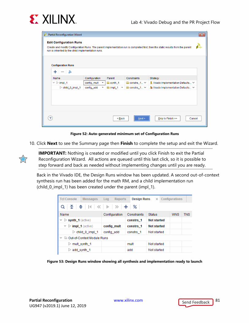
Lab 4: Vivado Debug and the PR Project Flow
Partial Reconfiguration www.xilinx.com 81 UG947 (v2019.1) June 12, 2019
Figure 52: Auto-generated minimum set of Configuration Runs
10. Click Next to see the Summary page then Finish to complete the setup and exit the Wizard.
IMPORTANT: Nothing is created or modified until you click Finish to exit the Partial
Reconfiguration Wizard. All actions are queued until this last click, so it is possible to
step forward and back as needed without implementing changes until you are ready.
Back in the Vivado IDE, the Design Runs window has been updated. A second out-of-context
synthesis run has been added for the math RM, and a child implementation run
(child_0_impl_1) has been created under the parent (impl_1).
Figure 53: Design Runs window showing all synthesis and implementation ready to launch
Send Feedback
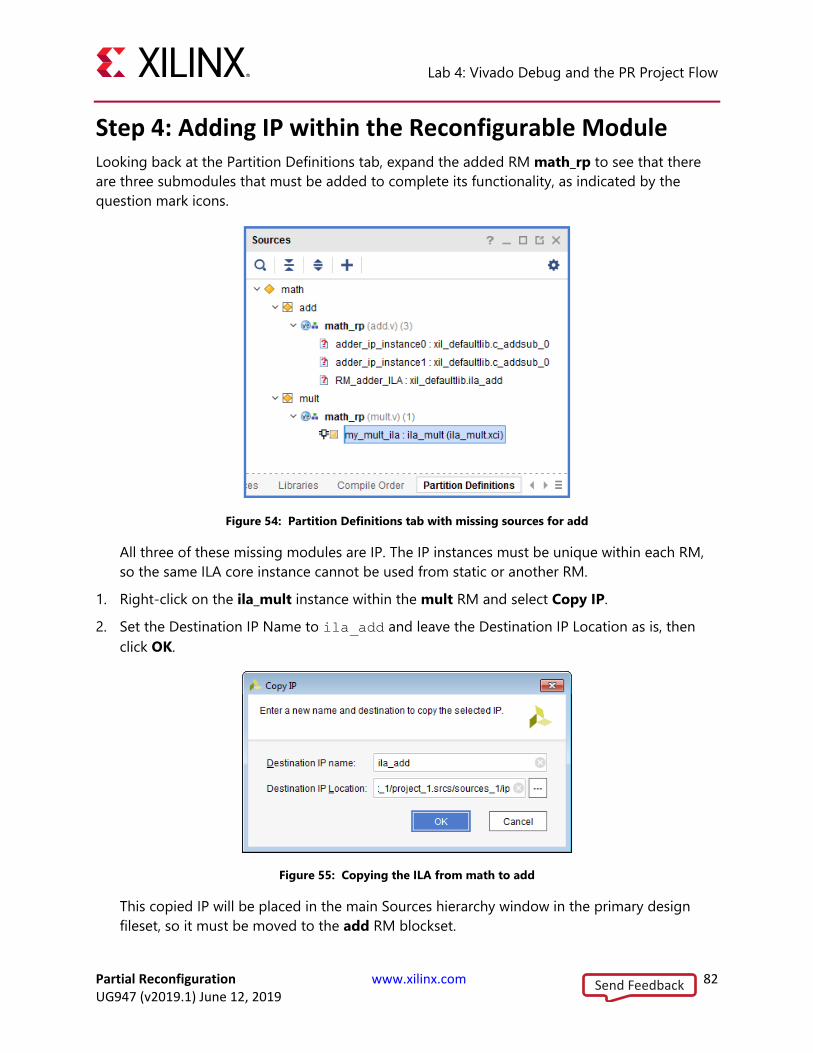
Lab 4: Vivado Debug and the PR Project Flow
Partial Reconfiguration www.xilinx.com 82 UG947 (v2019.1) June 12, 2019
Step 4: Adding IP within the Reconfigurable Module Looking back at the Partition Definitions tab, expand the added RM math_rp to see that there
are three submodules that must be added to complete its functionality, as indicated by the
question mark icons.
Figure 54: Partition Definitions tab with missing sources for add
All three of these missing modules are IP. The IP instances must be unique within each RM,
so the same ILA core instance cannot be used from static or another RM.
1. Right-click on the ila_mult instance within the mult RM and select Copy IP.
2. Set the Destination IP Name to ila_add and leave the Destination IP Location as is, then
click OK.
Figure 55: Copying the ILA from math to add
This copied IP will be placed in the main Sources hierarchy window in the primary design
fileset, so it must be moved to the add RM blockset.
Send Feedback
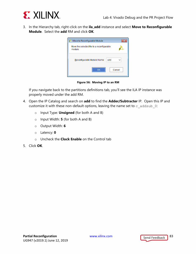
Lab 4: Vivado Debug and the PR Project Flow
Partial Reconfiguration www.xilinx.com 83 UG947 (v2019.1) June 12, 2019
3. In the Hierarchy tab, right-click on the ila_add instance and select Move to Reconfigurable
Module. Select the add RM and click OK.
Figure 56: Moving IP to an RM
If you navigate back to the partitions definitions tab, you’ll see the ILA IP instance was
properly moved under the add RM.
4. Open the IP Catalog and search on add to find the Adder/Subtracter IP. Open this IP and
customize it with these non-default options, leaving the name set to c_addsub_0:
o Input Type: Unsigned (for both A and B)
o Input Width: 5 (for both A and B)
o Output Width: 6
o Latency: 0
o Uncheck the Clock Enable on the Control tab
5. Click OK.
Send Feedback

Lab 4: Vivado Debug and the PR Project Flow
Partial Reconfiguration www.xilinx.com 84 UG947 (v2019.1) June 12, 2019
Figure 57: Customizing the Adder/Subtracter IP
6. Click Skip to complete IP generation.
Like with the ILA IP, this has been added to the main source set, so follow the same
procedure to move it to the add RM.
7. In the Hierarchy tab of the Sources window, right-click on the c_addsub_0 instance and
select Move to Reconfigurable Module.
Select the add RM and click OK.
Note that this IP is used for both adder function instances within the add RM. At this point, the
entire design has been loaded, and you are ready to move on to implementation.
Step 5: Synthesizing the Design and Creating a Floorplan Before launching synthesis, take a look at the naming convention that inserts the Debug Hubs
necessary for the Vivado Debug solution.
1. Open mult.v and examine the port list in this file.
The port list includes twelve ports that start with S_BSCAN_. These ports are used to
connect the Debug Hubs that are inserted in the static and reconfigurable parts of the
Send Feedback

Lab 4: Vivado Debug and the PR Project Flow
Partial Reconfiguration www.xilinx.com 85 UG947 (v2019.1) June 12, 2019
design. The insertion of these hubs is automatic. Connections are automatically made as
long as the port list matches this naming convention.
CAUTION! These exact port names must be used to have the inference occur. If the
port names differ at all, then the attributes shown in the comments of these RTL files
must be used to assign the new signal names to the debug properties as indicated.
With the design from section one open in the Vivado IDE, take a look at the Design Runs
window. The top-level design synthesis run (synth_1) and the parent implementation run
(impl_1) are marked “active.” The Flow Navigator actions apply to these active runs, so
clicking on Run Synthesis or Run Implementation will pull the design through only these
runs, as well as the OOC synthesis runs needed to complete them. You could select the child
implementation run, right-click, and select Launch Runs to pull through the entire flow, but
we’ll run synthesis separately here.
2. In the Flow Navigator, click Run Synthesis. When synthesis completes, select Open
Synthesized Design.
This action synthesizes all OOC modules, followed by synthesis of the top level design. This
is no different than any design with OOC modules (IP or otherwise).
3. Open the schematic for the post-synthesis view to see the insertions performed during
synthesis.
In the top level design, see that a dbg_hub instance was inserted. Its sl_* ports are
connected to the VIO debug core at the top level. Next, descend into the my_math
hierarchy to see that another dbg_hub instance has been inserted, with its sl_* ports
connected to the ILA debug core in that module. Note that this Reconfigurable Module is
the multiplier, as this is the schematic view of the active parent run.
Send Feedback

Lab 4: Vivado Debug and the PR Project Flow
Partial Reconfiguration www.xilinx.com 86 UG947 (v2019.1) June 12, 2019
Figure 58: dbg_hub_1 inserted within the mult RM
4. Select Layout > Floorplanning to put Vivado in floorplanning mode. Then in the Netlist
window, right click on the my_math instance and select Floorplanning > Draw Pblock.
Create a Pblock wherever you’d like. In the dialog box that appears, keep the name
pblock_my_math and leave only SLICE, DSP and BRAM resource types checked.
Figure 59: Drawing a Pblock for the my_math RP
Send Feedback

Lab 4: Vivado Debug and the PR Project Flow
Partial Reconfiguration www.xilinx.com 87 UG947 (v2019.1) June 12, 2019
If the region you have selected does not have enough resources of any particular type, these
resource types will appear in red in the Statistics tab of the Pblock Properties window. Make
adjustments as necessary, then save the floorplan. Remember, each RM contains an ILA core,
which will require BRAM. Also, this design has a high number of control sets, so the region
required may be a little bigger than expected. An area of at least 3000 CLBs plus a column of
BRAM is suggested.
5. Run PR-specific design rule checks by selecting Reports > Report DRC. To save time, you
can deselect all checkboxes other than the one for Partial Reconfiguration. Click OK to run.
Figure 60: Checking Partial Reconfiguration DRCs
Fix any errors that may appear. Advisory messages might appear for certain devices with
suggestions on how to improve the quality of the given Pblocks.
Send Feedback
Lab 4: Vivado Debug and the PR Project Flow
Partial Reconfiguration www.xilinx.com 88 UG947 (v2019.1) June 12, 2019
TIP: Run Partial Reconfiguration Design Rule Checks early and often.
6. Save your constraints by clicking Save Constraints in the top toolbar.
Step 6: Running the PR Configuration Analysis Report The PR Configuration Analysis tool compares each Reconfigurable Module that you select to
give you input on your PR design. It examines resource usage, floorplanning, clocking, and
timing metrics to help you manage the overall PR design. The PR Configuration Analysis tool is
run through the Tcl Console.
1. In the Tcl Console, cd into the project directory. Next, enter this command to run a report on
the two RMs available in this design:
report_pr_configuration_analysis -cells my_math -dcps
{./project_1.runs/add_synth_1/math_rp.dcp ./project_1.runs/mult_synth_1/math_rp.dcp}
Note: If your project is not named “project_1” you’ll need to adjust this in the Tcl
command.
This runs the analysis with the default settings, gathering data for the first three focus areas
listed below. Use the -help option to see that you can focus on three specific areas.
o The -complexity switch focuses the report on resource usage, including the
maximum resources required for the RP.
o The -clocking switch focuses the report on clock usage and loads for each RM.
o The -timing switch focuses the report on boundary interface timing details.
o The -rent switch adds rent metrics to the report, but can take a long time to run.
o The -file switch redirects the report to a file.
Examining the report in the Tcl Console, you will see a Complexity summary in section 2. It
shows the current RM (the multiplier), RMs 1 and 2 (the adder and multiplier, respectively),
and a column for the maximum. This table examines the resource utilization of each module
to find the maximum of each so you can construct Pblocks appropriately.
Note that the resource counts of RM1 and RM2 appear to be low. Above the report in the
log you will see a few critical warnings:
CRITICAL WARNING: [Project 1-486] Could not resolve non-primitive black
box cell 'math_rp_c_addsub_0' instantiated as 'adder_ip_instance0'
The post-synthesis checkpoints do not include the submodule IP as those were generated
out-of-context. In order to see the complete picture of each RM, these lower-level
checkpoints must be linked in, or the IP must be synthesized set to Global.
2. In the Partition Definitions tab, expand the hierarchy if necessary to be able to right click on
the my_mult_ila IP and select Generate Output Products.
Send Feedback

Lab 4: Vivado Debug and the PR Project Flow
Partial Reconfiguration www.xilinx.com 89 UG947 (v2019.1) June 12, 2019
3. Change the Synthesis Options value to Global, then click Apply and then Cancel.
4. Repeat this process for both IP under the adder module, my_add_ila and adder_ip. The
latter has two instances but this process only needs to happen once, as the IP instances are
identical.
5. Synthesis for these modules are now out of date. Select Run Synthesis in the Flow
Navigator. Accept all the dialogs that ask about resetting and resynthesizing all runs.
6. When synthesis completes, rerun the report_pr_configuration_analysis command
from step 1 and examine the log and results.
Step 7: Implementing the Design 1. In the Flow Navigator, select Run Implementation to run place and route on all
configurations.
This action runs implementation first for impl_1 and then for child_0_impl_1. In addition to
running place and route for the two runs with all the PR requirements in place, it does a few
more tasks specific to PR. After impl_1 completes, Vivado automatically:
o Writes a module-level (OOC) checkpoint for the routed multiplier RM.
o Carves out the logic in the RP to create a static-only design image. This is done by
calling update_design -black_box for the RP instance.
o Locks all placement and routing for this static-only design. This is done by calling
lock_design -level routing.
o Saves this locked static parent image to be reused for all child runs.
In addition, when the child run completes, a module-level checkpoint is created for the
routed adder RM. A locked static design image would be identical to the parent, so this step
is not necessary.
In Vivado projects, dependency management is handled by the Vivado IDE. If sources are
modified, any applicable runs will be marked out-of-date. The parent-child relationship
means these checks must understand dependencies. For example, if add.v is modified, only
its OOC synthesis run and the child implementation run would be marked out of date.
If only specific configuration runs are desired, these can be individually selected within the
Design Runs window. Note that a parent run must be completed successfully before a child
run can be launched, as the child run starts by importing the locked static design from the
parent.
Send Feedback
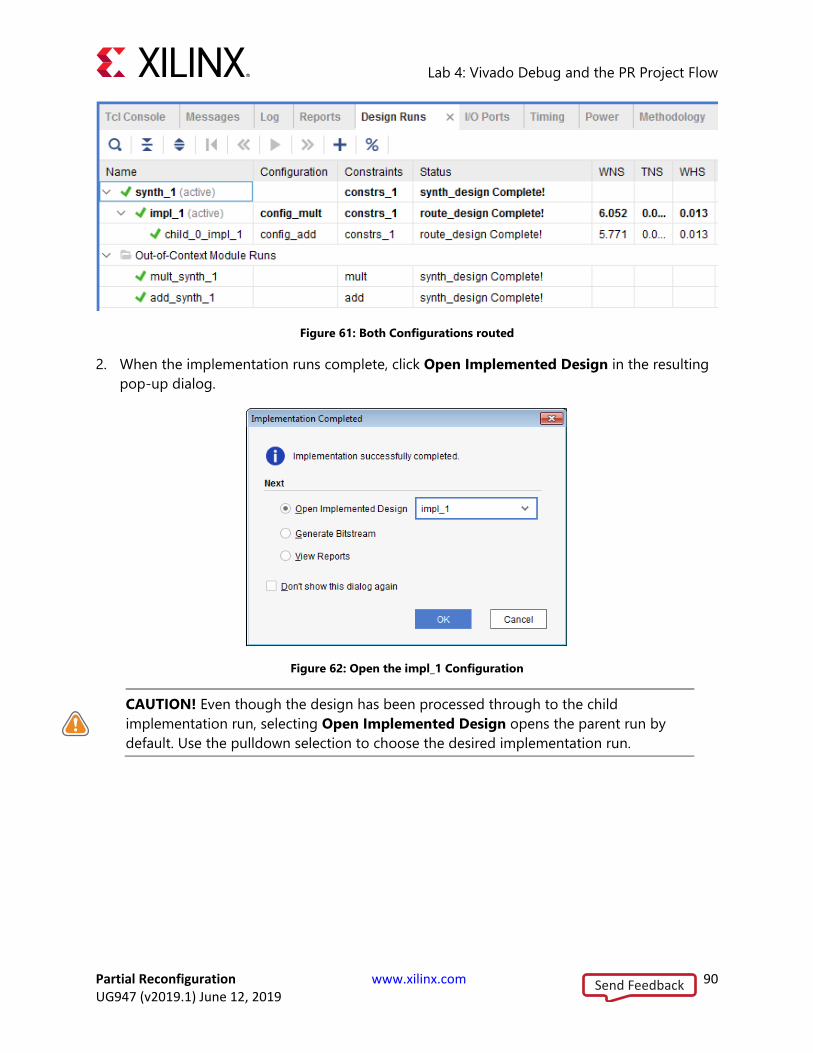
Lab 4: Vivado Debug and the PR Project Flow
Partial Reconfiguration www.xilinx.com 90 UG947 (v2019.1) June 12, 2019
Figure 61: Both Configurations routed
2. When the implementation runs complete, click Open Implemented Design in the resulting
pop-up dialog.
Figure 62: Open the impl_1 Configuration
CAUTION! Even though the design has been processed through to the child
implementation run, selecting Open Implemented Design opens the parent run by
default. Use the pulldown selection to choose the desired implementation run.
Send Feedback

Lab 4: Vivado Debug and the PR Project Flow
Partial Reconfiguration www.xilinx.com 91 UG947 (v2019.1) June 12, 2019
Figure 63: Device view of the routed parent design
This is the routed design for the multiplier configuration. Next, take a look at the frameset
of the placement and routing areas.
3. In the Tcl Console, cd to the current project directory (if you are not already there). Then run
these commands to source visualization scripts:
source project_1.runs/impl_1/hd_visual/pblock_my_math_Routing_AllTiles.tcl
highlight_objects -color yellow [get_selected_objects]
This first Tcl script identifies the frames that are valid for routing the reconfigurable part of
the design. Note that it extends to the height of the clock region(s) occupied by the Pblock,
and extends left and right by two programmable units. (Programmable units are pairs of
resource columns.)
Send Feedback

Lab 4: Vivado Debug and the PR Project Flow
Partial Reconfiguration www.xilinx.com 92 UG947 (v2019.1) June 12, 2019
4. Run these commands to identify the frameset used for placing the reconfigurable part of the
design.
source project_1.runs/impl_1/hd_visual/pblock_my_math_Placement_AllTiles.tcl
highlight_objects -color blue [get_selected_objects]
This highlighted region will be either the Pblock area itself, or an area just smaller than the
Pblock if the Pblock did not align with programmable units boundaries.
Your device view should look something like this:
Figure 64: The math RP highlighted to show placement (blue) and routing (yellow) boundaries
Static logic may be placed in the expanded routing region, which is now the remaining
yellow region. Static routing can use any resources in the device.
5. In the Flow Navigator, select Report Timing Summary and click OK to analyze the design
timing.
6. In the Timing tab, select the Design Timing Summary and click on the value for the Worst
Negative Slack (WNS) to bring up the top ten worst paths. Double-click on the first path to
open the timing summary on that path.
In this timing report, note that in the Clock Paths and the Data Path, there is a new column
labeled Partition that shows which partition (or boundary) that particular part of the path is
in.
Send Feedback
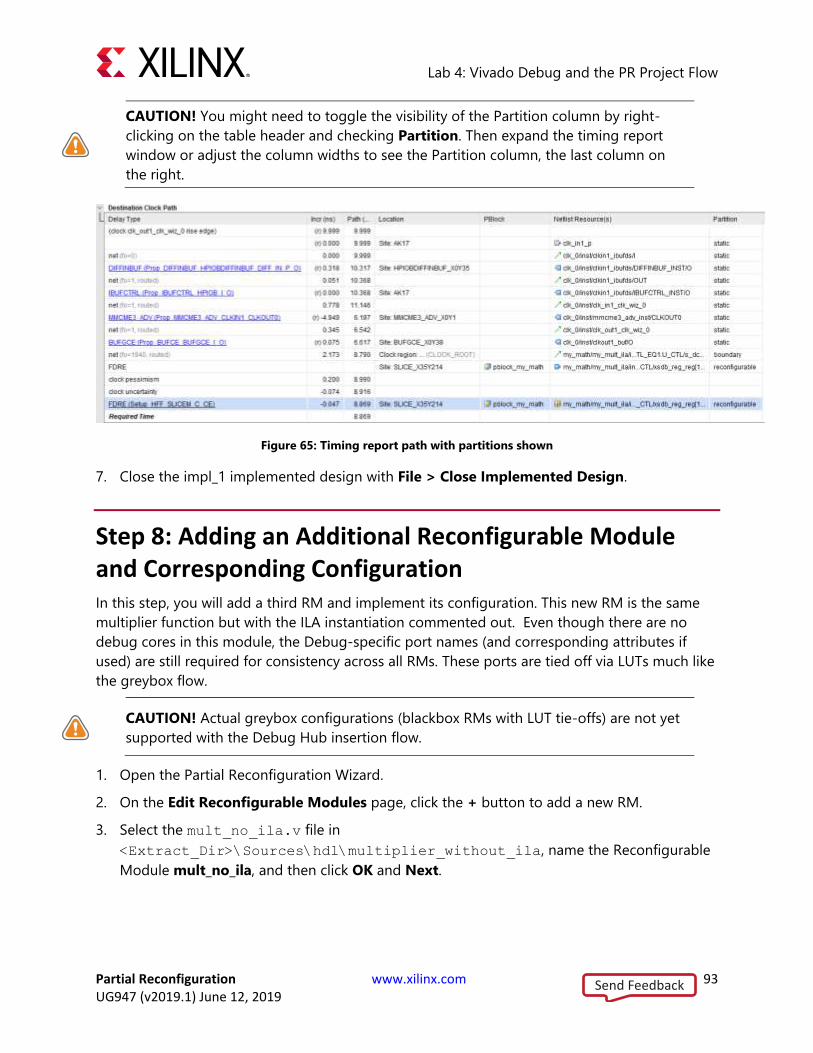
Lab 4: Vivado Debug and the PR Project Flow
Partial Reconfiguration www.xilinx.com 93 UG947 (v2019.1) June 12, 2019
CAUTION! You might need to toggle the visibility of the Partition column by right-
clicking on the table header and checking Partition. Then expand the timing report
window or adjust the column widths to see the Partition column, the last column on
the right.
Figure 65: Timing report path with partitions shown
7. Close the impl_1 implemented design with File > Close Implemented Design.
Step 8: Adding an Additional Reconfigurable Module and Corresponding Configuration In this step, you will add a third RM and implement its configuration. This new RM is the same
multiplier function but with the ILA instantiation commented out. Even though there are no
debug cores in this module, the Debug-specific port names (and corresponding attributes if
used) are still required for consistency across all RMs. These ports are tied off via LUTs much like
the greybox flow.
CAUTION! Actual greybox configurations (blackbox RMs with LUT tie-offs) are not yet
supported with the Debug Hub insertion flow.
1. Open the Partial Reconfiguration Wizard.
2. On the Edit Reconfigurable Modules page, click the + button to add a new RM.
3. Select the mult_no_ila.v file in
<Extract_Dir>\Sources\hdl\multiplier_without_ila, name the Reconfigurable
Module mult_no_ila, and then click OK and Next.
Send Feedback
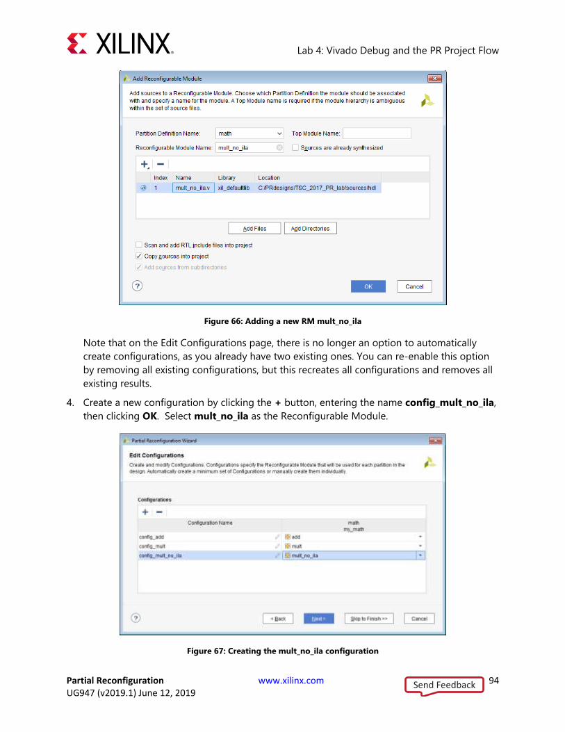
Lab 4: Vivado Debug and the PR Project Flow
Partial Reconfiguration www.xilinx.com 94 UG947 (v2019.1) June 12, 2019
Figure 66: Adding a new RM mult_no_ila
Note that on the Edit Configurations page, there is no longer an option to automatically
create configurations, as you already have two existing ones. You can re-enable this option
by removing all existing configurations, but this recreates all configurations and removes all
existing results.
4. Create a new configuration by clicking the + button, entering the name config_mult_no_ila,
then clicking OK. Select mult_no_ila as the Reconfigurable Module.
Figure 67: Creating the mult_no_ila configuration
Send Feedback
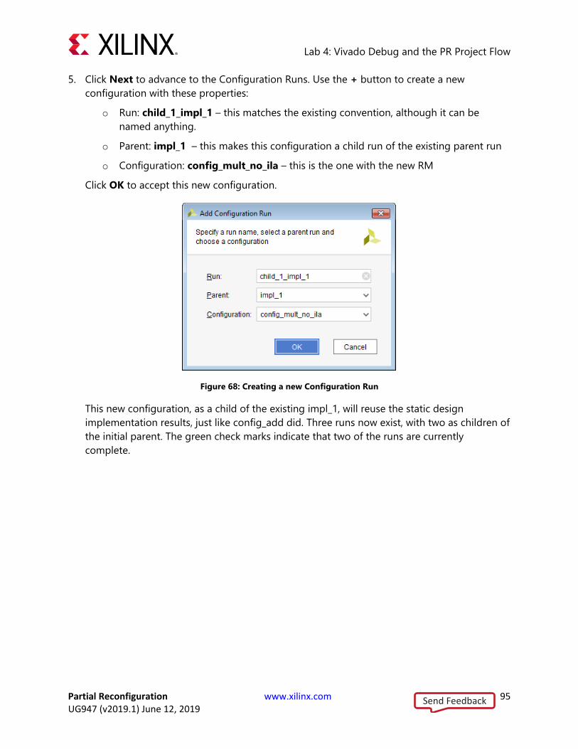
Lab 4: Vivado Debug and the PR Project Flow
Partial Reconfiguration www.xilinx.com 95 UG947 (v2019.1) June 12, 2019
5. Click Next to advance to the Configuration Runs. Use the + button to create a new
configuration with these properties:
o Run: child_1_impl_1 – this matches the existing convention, although it can be
named anything.
o Parent: impl_1 – this makes this configuration a child run of the existing parent run
o Configuration: config_mult_no_ila – this is the one with the new RM
Click OK to accept this new configuration.
Figure 68: Creating a new Configuration Run
This new configuration, as a child of the existing impl_1, will reuse the static design
implementation results, just like config_add did. Three runs now exist, with two as children of
the initial parent. The green check marks indicate that two of the runs are currently
complete.
Send Feedback

Lab 4: Vivado Debug and the PR Project Flow
Partial Reconfiguration www.xilinx.com 96 UG947 (v2019.1) June 12, 2019
Figure 69: The config_mult_no_ila configuration added as a new child run
6. Click Next then Finish to build this new configuration run.
Figure 70: New OOC synthesis run and Configuration run added
7. Select this new child implementation run, right-click and select Launch Runs. This runs OOC
synthesis on the mult_no_ila module, then implements this module within the context of the
locked static design.
Send Feedback
Lab 4: Vivado Debug and the PR Project Flow
Partial Reconfiguration www.xilinx.com 97 UG947 (v2019.1) June 12, 2019
CAUTION! Do not select Run Implementation from the Flow Navigator. It will rerun
all the implementation runs, even those that have completed.
8. Click Cancel on the dialog that opens after implementation completes.
Right-click on child_1_impl_1 and select Open Run. In the device view note two things:
a. The static logic is locked and therefore appears orange.
b. In the Design Runs tab, notice that the amount of logic in the RP Pblock is much smaller
than for the other configurations.
9. Select Tools > Schematic (or hit F4) to open the schematic view. Descend into the math_rp
instance to see that all the BSCAN ports are tied to LUTs and no ILA or Dbg_Hub cores are
inserted.
Step 9: Generating Bitstreams At this point, there are two steps remaining: the first is running PR Verify to compare the two
configurations to ensure consistency of the static part of the design images. This step is highly
recommended and will occur automatically within the Vivado project. The second step is to
generate the bitstreams themselves.
1. In the Flow Navigator, click Generate Bitstream. This action launches bitstream generation
on the active parent run, and launches PR Verify and then bitstream generation on the
implemented child runs.
2. This generates full and partial bitstreams for each configuration run.
3. When bitstream generation completes, select Open Hardware Manager.
Step 10: Connecting to the Board and Programming the FPGA 1. Open the hardware manager and connect to the target board.
This can be a local board or on a remote server. Exact details of how to accomplish this task
depends on your setup. You can interact with this design remotely via the VIO and ILA
debug cores.
2. Once you are connected to the hardware, right-click on the FPGA instance and select
Program Device. The top.bit file should be selected by default from the
project_1.runs/impl_1 directory. If it is not, select top.bit from the impl_1 project
run directory. Note that the top.ltx probes file is automatically selected. This is a complete
device bitstream that includes the multiplier RM.
Send Feedback

Lab 4: Vivado Debug and the PR Project Flow
Partial Reconfiguration www.xilinx.com 98 UG947 (v2019.1) June 12, 2019
3. Click on the hw_vio_1 dashboard tab. If it is not visible, open Dashboard Options and check
the hw_vio_1 box.
4. Press the + button and select all the probes from the add probes dialog box, then click OK.
Figure 71: Selecting probes for debug
5. Right click on the probes and set them up in the following manner:
o count_out_OBUF[7:0] bus – Radix: unsigned decimal
o count_out_OBUF[7:0] individual bits – LED: low value Red, high value Green
o pause_vio_out – Active High Button
o reset_vio_out – Active High Button
o toggle_vio_out – Active High Button
o vio_select – Toggle Button
The resulting dashboard looks like this:
Send Feedback

Lab 4: Vivado Debug and the PR Project Flow
Partial Reconfiguration www.xilinx.com 99 UG947 (v2019.1) June 12, 2019
Figure 72: Initial VIO dashboard for debugging
6. Change the vio_select value to a 1. This disables the buttons on the physical board and
enables the pause, reset and toggle buttons via the VIO.
7. Select the pause button by clicking on the Value field of pause_vio_out. You will see the
LED counter stop at a particular value. Take note of the unsigned binary value of the
count_out_OBUF. In this screenshot, the value is 12.
Send Feedback
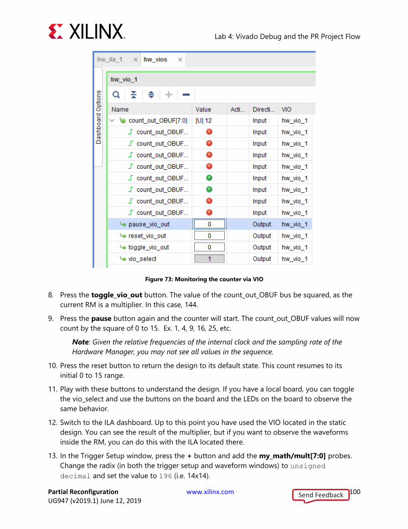
Lab 4: Vivado Debug and the PR Project Flow
Partial Reconfiguration www.xilinx.com 100 UG947 (v2019.1) June 12, 2019
Figure 73: Monitoring the counter via VIO
8. Press the toggle_vio_out button. The value of the count_out_OBUF bus be squared, as the
current RM is a multiplier. In this case, 144.
9. Press the pause button again and the counter will start. The count_out_OBUF values will now
count by the square of 0 to 15. Ex. 1, 4, 9, 16, 25, etc.
Note: Given the relative frequencies of the internal clock and the sampling rate of the
Hardware Manager, you may not see all values in the sequence.
10. Press the reset button to return the design to its default state. This count resumes to its
initial 0 to 15 range.
11. Play with these buttons to understand the design. If you have a local board, you can toggle
the vio_select and use the buttons on the board and the LEDs on the board to observe the
same behavior.
12. Switch to the ILA dashboard. Up to this point you have used the VIO located in the static
design. You can see the result of the multiplier, but if you want to observe the waveforms
inside the RM, you can do this with the ILA located there.
13. In the Trigger Setup window, press the + button and add the my_math/mult[7:0] probes.
Change the radix (in both the trigger setup and waveform windows) to unsigned
decimal and set the value to 196 (i.e. 14x14).
Send Feedback
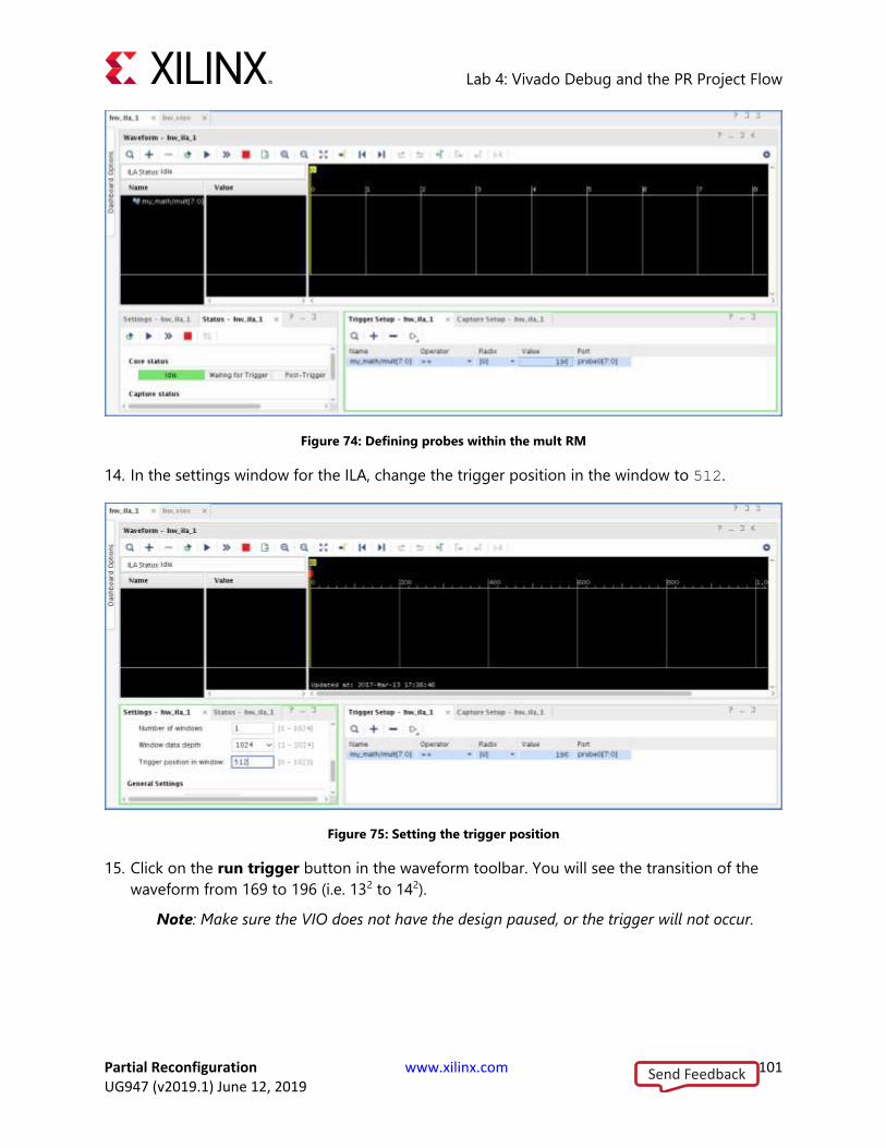
Lab 4: Vivado Debug and the PR Project Flow
Partial Reconfiguration www.xilinx.com 101 UG947 (v2019.1) June 12, 2019
Figure 74: Defining probes within the mult RM
14. In the settings window for the ILA, change the trigger position in the window to 512.
Figure 75: Setting the trigger position
15. Click on the run trigger button in the waveform toolbar. You will see the transition of the
waveform from 169 to 196 (i.e. 132 to 142).
Note: Make sure the VIO does not have the design paused, or the trigger will not occur.
Send Feedback
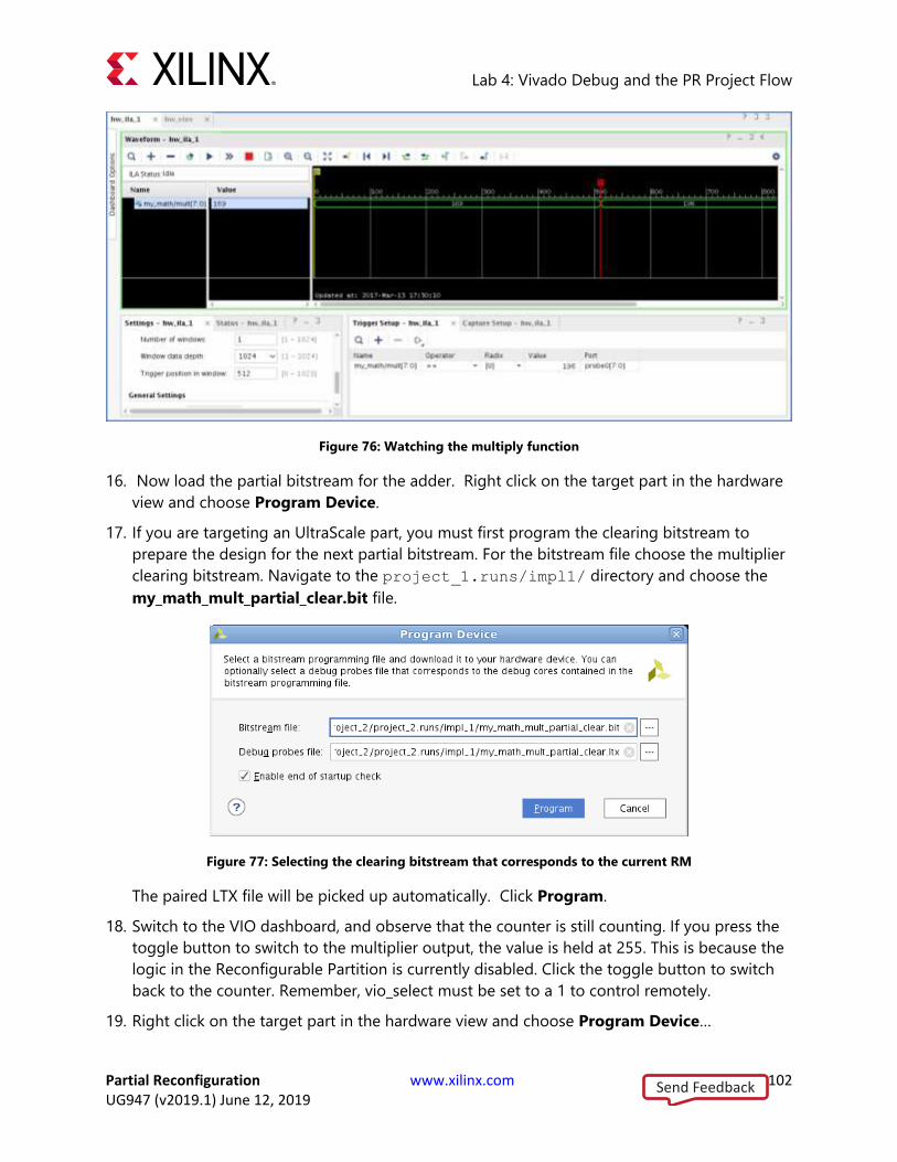
Lab 4: Vivado Debug and the PR Project Flow
Partial Reconfiguration www.xilinx.com 102 UG947 (v2019.1) June 12, 2019
Figure 76: Watching the multiply function
16. Now load the partial bitstream for the adder. Right click on the target part in the hardware
view and choose Program Device.
17. If you are targeting an UltraScale part, you must first program the clearing bitstream to
prepare the design for the next partial bitstream. For the bitstream file choose the multiplier
clearing bitstream. Navigate to the project_1.runs/impl1/ directory and choose the
my_math_mult_partial_clear.bit file.
Figure 77: Selecting the clearing bitstream that corresponds to the current RM
The paired LTX file will be picked up automatically. Click Program.
18. Switch to the VIO dashboard, and observe that the counter is still counting. If you press the
toggle button to switch to the multiplier output, the value is held at 255. This is because the
logic in the Reconfigurable Partition is currently disabled. Click the toggle button to switch
back to the counter. Remember, vio_select must be set to a 1 to control remotely.
19. Right click on the target part in the hardware view and choose Program Device…
Send Feedback
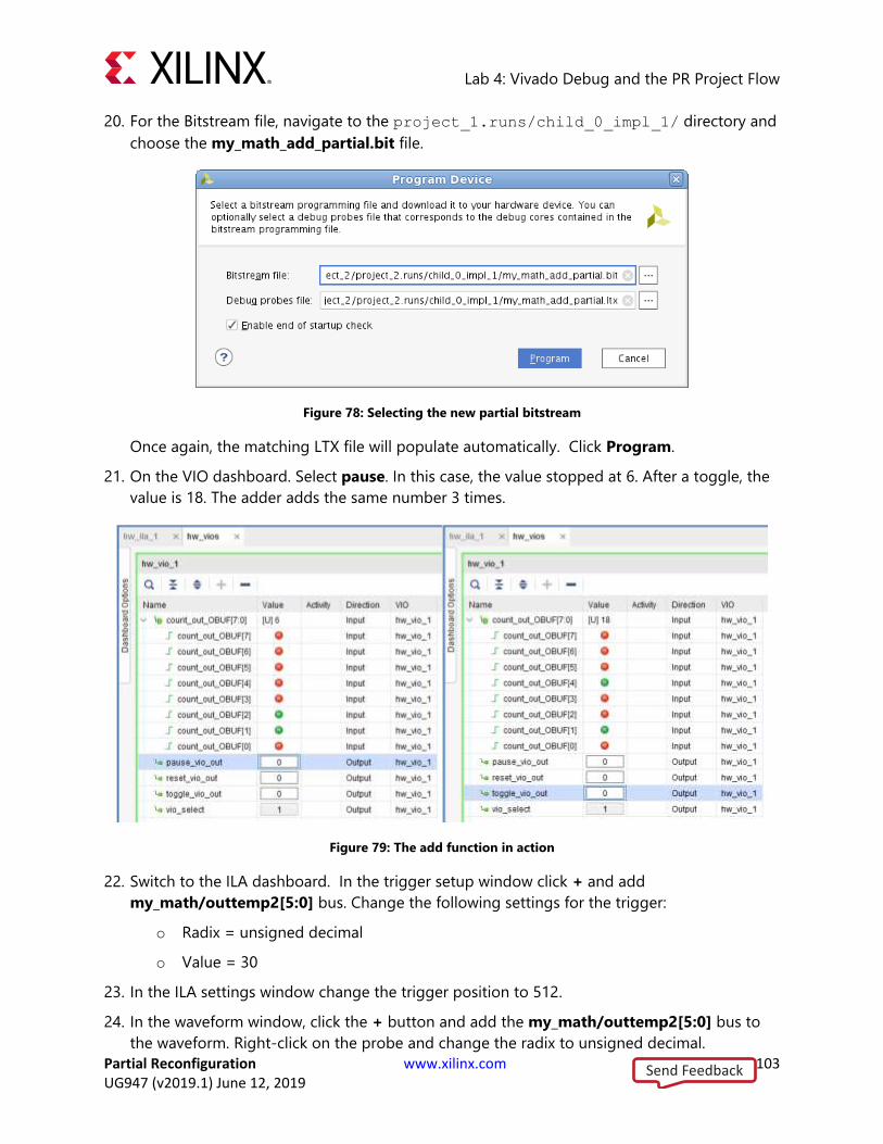
Lab 4: Vivado Debug and the PR Project Flow
Partial Reconfiguration www.xilinx.com 103 UG947 (v2019.1) June 12, 2019
20. For the Bitstream file, navigate to the project_1.runs/child_0_impl_1/ directory and
choose the my_math_add_partial.bit file.
Figure 78: Selecting the new partial bitstream
Once again, the matching LTX file will populate automatically. Click Program.
21. On the VIO dashboard. Select pause. In this case, the value stopped at 6. After a toggle, the
value is 18. The adder adds the same number 3 times.
Figure 79: The add function in action
22. Switch to the ILA dashboard. In the trigger setup window click + and add
my_math/outtemp2[5:0] bus. Change the following settings for the trigger:
o Radix = unsigned decimal
o Value = 30
23. In the ILA settings window change the trigger position to 512.
24. In the waveform window, click the + button and add the my_math/outtemp2[5:0] bus to
the waveform. Right-click on the probe and change the radix to unsigned decimal.
Send Feedback
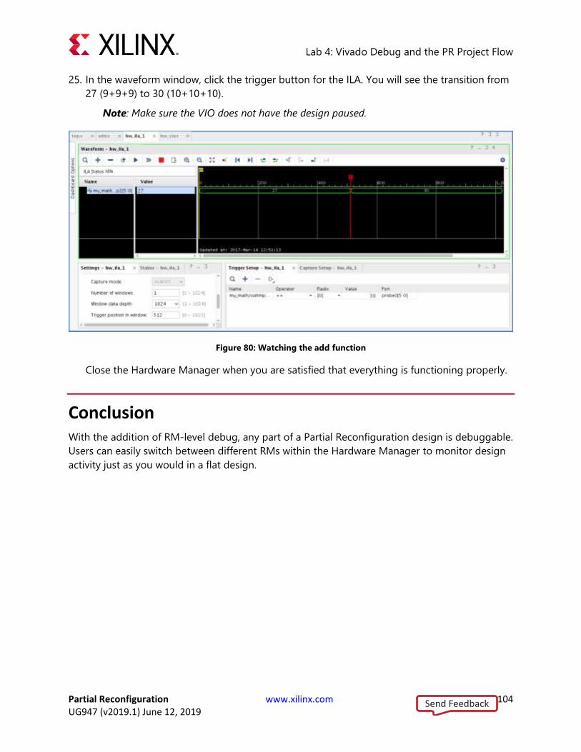
Lab 4: Vivado Debug and the PR Project Flow
Partial Reconfiguration www.xilinx.com 104 UG947 (v2019.1) June 12, 2019
25. In the waveform window, click the trigger button for the ILA. You will see the transition from
27 (9+9+9) to 30 (10+10+10).
Note: Make sure the VIO does not have the design paused.
Figure 80: Watching the add function
Close the Hardware Manager when you are satisfied that everything is functioning properly.
Conclusion With the addition of RM-level debug, any part of a Partial Reconfiguration design is debuggable.
Users can easily switch between different RMs within the Hardware Manager to monitor design
activity just as you would in a flat design.
Send Feedback
Partial Reconfiguration www.xilinx.com 105 UG947 (v2019.1) June 12, 2019
Lab 5: Partial Reconfiguration Controller IP for 7 Series Devices
Step 1: Extracting the Tutorial Design Files 1. To obtain the tutorial design file, see Tutorial Design Description.
2. Navigate to \prc_7s in the extracted files. The prc_7s data directory is referred to
throughout the lab as the <Extract_Dir>.
Step 2: Customizing the Partial Reconfiguration Controller IP The PRC IP requires a few details to be entered during the customization process. Identifying all
information regarding each Reconfigurable Partition (RP) and Reconfigurable Module (RM)
creates a fully populated controller that understands the entirety of the reconfiguration needs of
the target FPGA. Within this IP, reconfigurable portions of the design are referred to as Virtual
Sockets, which encompasses the RP along with all associated static logic used to manage it, such
as decoupling or handshaking logic. While the core parameters are customizable during
operation, the more that can be entered during this step, the better. This allows the front-end
design description to more accurately match the final implemented design.
1. Open the Vivado IDE and click the Manage IP task, and select New IP Location. Enter the
following details before clicking Finish:
• Part: Click on Boards to select your target. This lab supports the KC705, VC707 and
VC709.
• IP Location: <Extract_Dir>/Sources/ip
2. In the IP Catalog, expand the Partial Reconfiguration category to double-click on the Partial
Reconfiguration Controller IP.
Send Feedback

Lab 5: Partial Reconfiguration Controller IP for 7 Series Devices
Partial Reconfiguration www.xilinx.com 106 UG947 (v2019.1) June 12, 2019
Figure 81: The Partial Reconfiguration Controller as shown in the IP Catalog
The PR Controller IP GUI has four tabs on the left side, providing feedback on the current
configuration of the IP. The default pane is labeled Validation, and shows any errors that
might arise as the core parameters are entered. The core does not compile if errors exist.
There are two tabs on the right side of the GUI where all customization is done. Most of the
information is entered on the Virtual Socket Manager Options tab.
3. Leave the component name as prc_0. The version of the PRC used in the final design will be
automatically compiled in Step 3: Compiling the Design.
4. On the Global Options tab, make three changes:
a. Set the polarity of reset and icap_reset = 1
b. Specify the CAP arbitration protocol = 1) Latency has not been added to arbiter
signals
c. Specify the number of Clock domain crossing stages = 2
Make sure that the Managed device type is set to 7 Series. The PRC GUI should now look
like this:
Figure 82: Component Name and Global Options completed
Send Feedback

Lab 5: Partial Reconfiguration Controller IP for 7 Series Devices
Partial Reconfiguration www.xilinx.com 107 UG947 (v2019.1) June 12, 2019
Note that this PR Controller can manage Virtual Sockets on 7 series, UltraScale, UltraScale+
devices. This IP is not limited to managing PR on the same device on which it resides. It can
connect to an ICAP on another device to manage its reconfiguration.
Figure 83: Example of a multi-chip solution using the PRC
5. Next, switch to the Virtual Socket Manager Options tab to define information about the
Virtual Sockets and their Reconfigurable Modules.
The PRC IP is preloaded with one Virtual Socket with one Reconfigurable Module to get you
started.
First, define the Virtual Socket Manager (VSM) for the Shift functionality.
6. Rename the current VSM from VS_0 to vs_shift in the Virtual Socket Name field.
7. Rename the current RM from RM_0 to rm_shift_left in the Reconfigurable Module Name
field.
CAUTION!
• Underscores are not visible in the Virtual Socket Manager and Reconfigurable
Module pull-down dialogs. The Name (ID) label below the pull-down shows
this more accurately.
• To accept a new value in any field in the GUI, simply click in any other field in
the GUI or press the Tab key. Do NOT press Enter, as this will trigger
compilation of the IP.
8. Click the New Reconfigurable Module button to create a new RM for this VSM. Notice the
form has changed. The new, generic, Reconfigurable Module Name is RM_1. Name it
rm_shift_right.
Send Feedback
Lab 5: Partial Reconfiguration Controller IP for 7 Series Devices
Partial Reconfiguration www.xilinx.com 108 UG947 (v2019.1) June 12, 2019
TIP: Up to 128 Reconfigurable Modules can be managed by a single Virtual Socket
Manager.
9. Configure the vs_shift VSM to have the following properties:
• Has Status Channel = checked
• Has PoR RM = rm_shift_right
• Number of RMs allocated = 4
The PoR RM indicates which RM is contained within the initial full-design configuration file,
so the VSM knows which triggers and events are appropriate upon startup of the FPGA. The
VSM tracks the current active Reconfigurable Module in its socket.
Even through you have only defined two RMs for this Virtual Socket, you have set aside
space for four in total. This allows for expansion later on. Additional Reconfigurable Modules
can be identified using the AXI4-Lite interface, but only if spaces have been reserved for
them.
10. For each of these RMs, enter the following values. Use the Reconfigurable Module to
configure pull-down to switch between the two RMs.
• For rm_shift_left:
o Reset type = Active High
o Duration of Reset = 3
• For rm_shift_right:
o Reset type = Active High
o Duration of Reset = 10
Note: The different reset durations are given to show that these can be independently
assigned, as each RM may have different requirements. Reset durations are measured in
clock cycles.
11. For each RM, assign a bitstream size and location to identify where it will reside in the BPI
flash device. These values differ based on the target board.
• When targeting the KC705:
o For rm_shift_left:
− Bitstream 0 address = 0x00AEA000
− Bitstream 0 size (bytes) = 482828
o For rm_shift_right:
− Bitstream 0 address = 0x00B60000
− Bitstream 0 size (bytes) = 482828
Send Feedback
Lab 5: Partial Reconfiguration Controller IP for 7 Series Devices
Partial Reconfiguration www.xilinx.com 109 UG947 (v2019.1) June 12, 2019
• When targeting the VC707:
o For rm_shift_left:
− Bitstream 0 address = 0x01355C00
− Bitstream 0 size (bytes) = 708260
o For rm_shift_right:
− Bitstream 0 address = 0x01402C00
− Bitstream 0 size (bytes) = 708260
• When targeting the VC709:
o For rm_shift_left:
− Bitstream 0 address = 0x00800000
− Bitstream 0 size (bytes) = 889252
o For rm_shift_right:
− Bitstream 0 address = 0x008D9400
− Bitstream 0 size (bytes) = 889252
This information is typically not known early in design cycles, as bitstream size is based on
the size and composition of the Reconfigurable Partition Pblock, and bitstream address is
based on storage details. Until the design is to be tested on silicon, these can be set to 0. As
the design settles and hardware testing with the PRC is set to begin, this information can be
added. The bitstream address information must match the information passed during PROM
file generation. Certain bitstream generation options, most notably bitstream compression,
can lead to variations in the final bitstream size for different configurations, even for the
same Reconfigurable Partition.
12. Define the Trigger Options for the Shift functionality:
• Number of Hardware Triggers = 4
• Number of Triggers allocated = 4
The four trigger assignments are done automatically. These can be modified during device
operation using AXI4-Lite, which is especially useful when you have added a new RM
through the same mechanism during a field system upgrade.
At this point, the IP GUI should look like this (showing rm_shift_left here):
Send Feedback
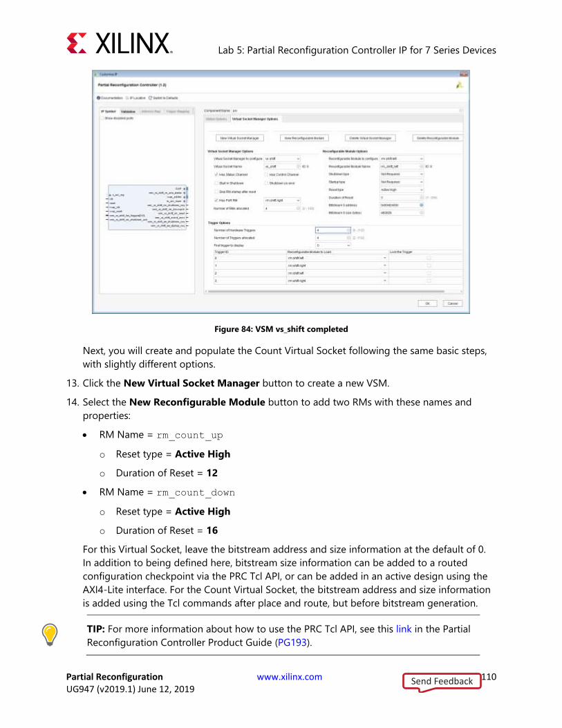
Lab 5: Partial Reconfiguration Controller IP for 7 Series Devices
Partial Reconfiguration www.xilinx.com 110 UG947 (v2019.1) June 12, 2019
Figure 84: VSM vs_shift completed
Next, you will create and populate the Count Virtual Socket following the same basic steps,
with slightly different options.
13. Click the New Virtual Socket Manager button to create a new VSM.
14. Select the New Reconfigurable Module button to add two RMs with these names and
properties:
• RM Name = rm_count_up
o Reset type = Active High
o Duration of Reset = 12
• RM Name = rm_count_down
o Reset type = Active High
o Duration of Reset = 16
For this Virtual Socket, leave the bitstream address and size information at the default of 0.
In addition to being defined here, bitstream size information can be added to a routed
configuration checkpoint via the PRC Tcl API, or can be added in an active design using the
AXI4-Lite interface. For the Count Virtual Socket, the bitstream address and size information
is added using the Tcl commands after place and route, but before bitstream generation.
TIP: For more information about how to use the PRC Tcl API, see this link in the Partial
Reconfiguration Controller Product Guide (PG193).
Send Feedback
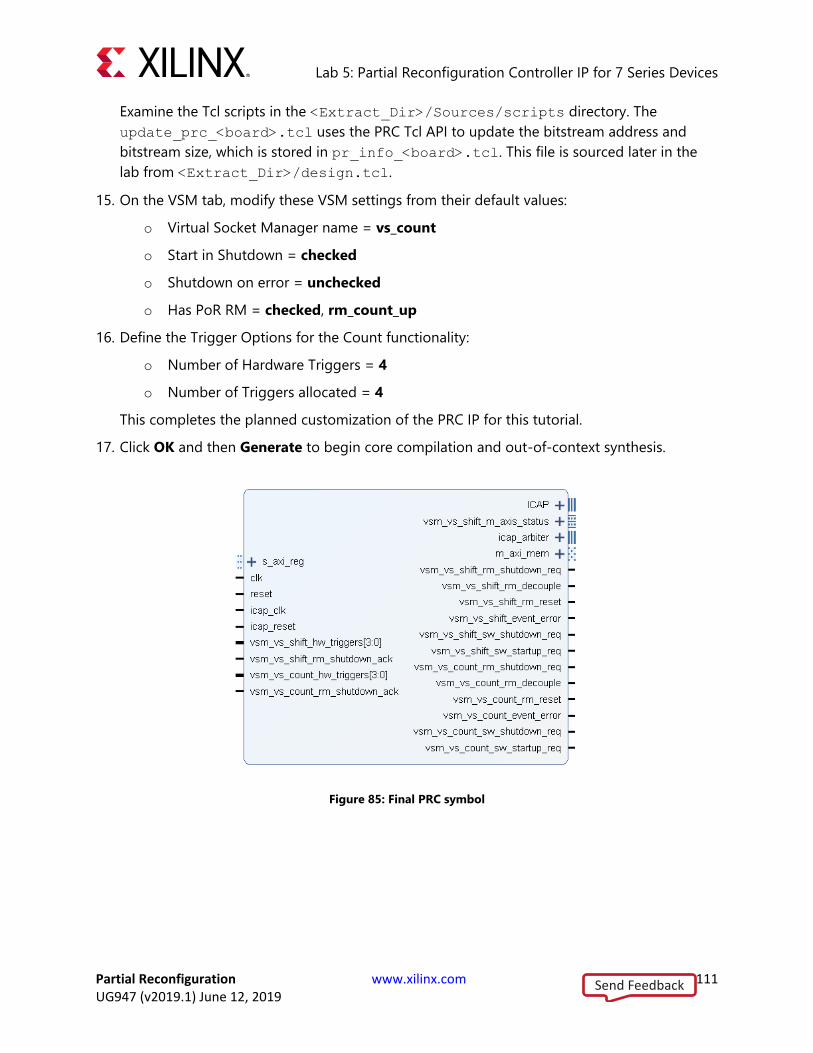
Lab 5: Partial Reconfiguration Controller IP for 7 Series Devices
Partial Reconfiguration www.xilinx.com 111 UG947 (v2019.1) June 12, 2019
Examine the Tcl scripts in the <Extract_Dir>/Sources/scripts directory. The
update_prc_<board>.tcl uses the PRC Tcl API to update the bitstream address and
bitstream size, which is stored in pr_info_<board>.tcl. This file is sourced later in the
lab from <Extract_Dir>/design.tcl.
15. On the VSM tab, modify these VSM settings from their default values:
o Virtual Socket Manager name = vs_count
o Start in Shutdown = checked
o Shutdown on error = unchecked
o Has PoR RM = checked, rm_count_up
16. Define the Trigger Options for the Count functionality:
o Number of Hardware Triggers = 4
o Number of Triggers allocated = 4
This completes the planned customization of the PRC IP for this tutorial.
17. Click OK and then Generate to begin core compilation and out-of-context synthesis.
Figure 85: Final PRC symbol
Send Feedback
Lab 5: Partial Reconfiguration Controller IP for 7 Series Devices
Partial Reconfiguration www.xilinx.com 112 UG947 (v2019.1) June 12, 2019
Step 3: Compiling the Design The PR Controller IP is created, but the design is not yet compiled. In order to create the PROM
image with all the necessary full and partial images, source the following scripts in Tcl mode
using the commands below.
IMPORTANT: Before running this Tcl script, open it to set the value of the xboard
variable. KC705 is the default, but VC707 or VC709 can be selected.
1. vivado -mode tcl -source design.tcl
Sourcing design.tcl generates all the necessary IP (including the PRC), synthesizes and
implements the entire design (three configurations), updates the vs_count VSM using the
PRC Tcl API, and generates bitstreams.
Note that the customization of the IP is scripted. Examine the gen_ip_<board>.tcl script
(in <Extract_Dir>/Sources/scripts) to see all these parameters defined for
automated IP creation, the PRC, and others. The PRC instance you create using the IP GUI is
not actually used for the full design processing, so you do not have to complete Section 1 to
compile the entire design.
2. vivado -mode tcl -source create_prom_file_<board>.tcl
Sourcing the board-specific create_prom_file.tcl creates the PROM image for the
target board. This script contains hard-coded values for bitstream address for the entire
project. If this design is modified in such a way that changes bitstream sizes, full or partial,
then these values must also change. Changes that affect bitstream sizes include changing
the target device, changing the size or shape of the Pblocks, or introducing bitstream
options such as compression or per-frame CRC.
This script defines PROM file options by setting properties and then making calls to
write_cfgmem. The PRC works in byte addresses because the data is stored in bytes in AXI.
This linear flash PROM uses half word addresses because it stores data in half words (16
bits). Divide the ROM address by 2 to get the AXI address. For example, the shift_left address
for the KC705 is given as 00AEA000 in during PRC customization and 00575000 (half that
value) for write_cfgmem. Note that the starting addresses are always multiples of 1024
(0x0400) to ensure that each bitstream starts on a byte address boundary. Also note that the
initial configuration file for the VC709 is compressed in order to fit in the linear flash; the
address for the first partial bitstream that follows is padded to allow expansion of that initial
configuration file.
Send Feedback

Lab 5: Partial Reconfiguration Controller IP for 7 Series Devices
Partial Reconfiguration www.xilinx.com 113 UG947 (v2019.1) June 12, 2019
Supplied in the lab directory is a file called prc_bitstream_sizes_lab5.xlsx. In this
file, bitstream sizes are entered by the user based in the yellow highlighted fields. It
calculates the starting address in hex for each partial bitstream at the next byte boundary.
Values in blue are to be supplied for PR Controller IP customization, in either the PRC IP GUI,
in the gen_ip_<board>.tcl script, or in pr_info_<board>.tcl which is used for post-
route API modification. The values in green are addresses divided by two to be used in
PROM file generation in the create_prom_file_<board>.tcl script.
Step 4: Setting up the Board Once the partially reconfigurable design is in operation, you can connect to and communicate
with the core to check status, deliver triggers and make modifications.
1. Prepare the target board for programming.
a. Connect the JTAG port to your computer via the micro-USB connection.
o For the KC705: U59
o For the VC707 or VC709: U26
b. Set the configuration mode to 010 (BPI) by setting the Address DIP Switch (SW13) to
00010 (bit 4 is high).
c. Turn on the power to the board.
2. Open the Vivado IDE.
3. Select Flow > Open Hardware Manager
4. Click on the Open Target link and select Auto Connect for the device to be recognized.
5. To program the BPI configuration flash, right-click the device (e.g. xc7k325t_0) and select
Add Configuration Memory Device.
6. From the list shown, select the appropriate linear BPI flash and click OK twice.
o For the KC705, select 28f00ap30t
o For the VC707 or VC709, select 28f00ag18f
7. In the Configuration file field, search the tutorial directory for pr_prom.mcs found in the
bitstreams subdirectory. Click OK to select this file, and then click OK to program the flash.
At this point, the board is ready to operate with the tutorial design. Any power-cycle or hard
reset automatically programs the Xilinx FPGA with this sample design.
Send Feedback
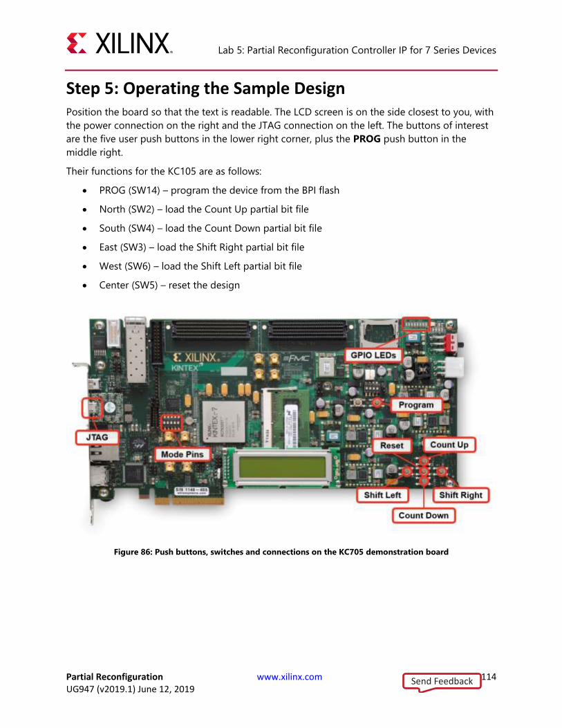
Lab 5: Partial Reconfiguration Controller IP for 7 Series Devices
Partial Reconfiguration www.xilinx.com 114 UG947 (v2019.1) June 12, 2019
Step 5: Operating the Sample Design Position the board so that the text is readable. The LCD screen is on the side closest to you, with
the power connection on the right and the JTAG connection on the left. The buttons of interest
are the five user push buttons in the lower right corner, plus the PROG push button in the
middle right.
Their functions for the KC105 are as follows:
• PROG (SW14) – program the device from the BPI flash
• North (SW2) – load the Count Up partial bit file
• South (SW4) – load the Count Down partial bit file
• East (SW3) – load the Shift Right partial bit file
• West (SW6) – load the Shift Left partial bit file
• Center (SW5) – reset the design
Figure 86: Push buttons, switches and connections on the KC705 demonstration board
Send Feedback

Lab 5: Partial Reconfiguration Controller IP for 7 Series Devices
Partial Reconfiguration www.xilinx.com 115 UG947 (v2019.1) June 12, 2019
Their functions for the VC707 and VC709 are as follows:
• PROG (SW9) – program the device from the BPI flash
• North (SW3) – load the Count Up partial bit file
• South (SW5) – load the Count Down partial bit file
• East (SW4) – load the Shift Right partial bit file
• West (SW7) – load the Shift Left partial bit file
• Center (SW6) – reset the design
Figure 87: Push buttons, switches and connections on the VC707 demonstration board
Send Feedback

Lab 5: Partial Reconfiguration Controller IP for 7 Series Devices
Partial Reconfiguration www.xilinx.com 116 UG947 (v2019.1) June 12, 2019
Figure 88: Push buttons, switches and connections on the VC709 demonstration board
8. Program the FPGA by pressing the PROG pushbutton. The 8 GPIO LEDs in the upper-right
corner will start operation after the DONE LED goes high.
At this point, the four bits on the left of the GPIO bank are counting up, and the four bits on
the right are shifting to the right.
9. Press the Shift Left and Shift Right buttons alternately.
With each push, a partial bit file is pulled from the BPI flash by the PRC and delivered to the
ICAP, changing the functionality in that Reconfigurable Partition. When this happens, the
LED shift direction changes, depending on the button pushed.
10. Press the Count Down and Count Up buttons alternately.
With each push, nothing happens. When configuring the PR Controller, the Counter Virtual
Socket was programmed to begin in Shutdown mode. It does not respond to any hardware
or software triggers until it is moved to Active mode.
Step 6: Querying the PRC in the FPGA In this step, you interact with the core via JTAG from the Hardware Manager to understand the
status of the core and issue software triggers.
In the Vivado Hardware Manager, you might need to select Refresh Device to establish the link
to the device over the JTAG connection. Notice the XADC as well as 6 ILA cores and the hw_axi
link shown under the device in the Hardware view.
Send Feedback
Lab 5: Partial Reconfiguration Controller IP for 7 Series Devices
Partial Reconfiguration www.xilinx.com 117 UG947 (v2019.1) June 12, 2019
1. In the Tcl Console, cd into the PRC tutorial directory then source the AXI4-Lite command Tcl
script.
source ./Sources/scripts/axi_lite_procs.tcl
This enables a set of procedures that make the subsequent interaction with the PRC easier.
Examine this file to see how these procedures are defined. Note that these are written
explicitly (hard-coded) for this design, the references to Virtual Sockets in any other design
will need to be modified. For more information on this topic, consult the Partial
Reconfiguration Controller Product Guide (PG193).
2. Source the procedure to establish communication with the PRC.
prc_jtag_setup
3. Check the state of each Virtual Socket to see if they are in Shutdown or not.
is_vsm_in_shutdown vs_shift
is_vsm_in_shutdown vs_count
You should see that the Shift Virtual Socket is in Active mode (value = 0), and the Count
Virtual Socket is in Shutdown mode (value = 1).
4. Examine the status of each Virtual Socket.
prc_decode_status vs_shift
prc_decode_status vs_count
Before examining the data returned, reference Table 2-4 in this link of the Partial
Reconfiguration Controller Product Guide (PG193). The table in that section defines the
values in the STATUS register. While this is a 32-bit register, you only need to pay attention
to the lowest 24 bits, as the upper 8 bits are used for Virtual Socket Managers (VSM) in
UltraScale devices.
The status of vs_shift is 263, which is 0000_0000_0000_0001_0000_0111 in binary.
The status for vs_shift may also be 7, where the only difference is that RM_ID is now 0.
o RM_ID (bits 23:8) = 1. This means RM 1 is loaded (rm_shift_right). It may also
appear as RM_ID (bits 24:8) = 0. This means RM 0 is loaded (rm_shift_left).
o SHUTDOWN (bit 7) = 0. This VSM is not in the shutdown state.
o ERROR (bits 6:3) = 0000. There are no errors.
o STATE (bits 2:0) = 111. The Virtual Socket is full.
The status of vs_count is 129, which is 0000_0000_0000_0000_1000_0001 in binary.
o RM_ID (bits 23:8) = 0. This means RM 0 is loaded (rm_count_up).
o SHUTDOWN (bit 7) = 1. This VSM is in the shutdown state.
o ERROR (bits 6:3) = 0000. There are no errors.
o STATE (bits 2:0) = 001. RM_SHUTDOWN_ACK is 1, as this VSM is executing the
hardware shutdown step.
Send Feedback

Lab 5: Partial Reconfiguration Controller IP for 7 Series Devices
Partial Reconfiguration www.xilinx.com 118 UG947 (v2019.1) June 12, 2019
These explicit details are reported in the breakdown of the status register in the return value
from this Tcl proc.
5. Send a software trigger to the Shift Virtual Socket.
prc_send_sw_trigger vs_shift 0
prc_send_sw_trigger vs_shift 1
Remember that values of 0 and 2 correspond to shift left, and values of 1 and 3 correspond
to shift right, as defined during PRC customization.
6. Check the configurations of the RMs for the Count Virtual Socket.
prc_show_rm_configuration vs_count 0
prc_show_rm_configuration vs_count 1
The values for the bitstream sizes and address are reported here. These values could then be
modified to account for necessary adjustments to the size or location of the bitstream.
Different indices can be added to insert new RMs. Note that this query cannot be done for
vs_shift, as the vs_shift VSM is not in the shutdown state.
7. Move the Count Virtual Socket Manager into active mode.
prc_restart_vsm_no_status vs_count
The Count Up and Count Down pushbuttons can now be used to load these partial
bitstreams using the PR Controller.
Step 7: Modifying the PRC in the FPGA In the final step, you add a new Reconfigurable Module to the Shifter VSM. In the
create_prom_file_<board>.tcl script, you can see that two black box modules have
already been generated. These represent two new RMs that may have been created after the
static design was deployed to the field. You modify the PRC settings to access one of these RMs
by assigning the size, address, properties and trigger conditions.
1. Shut down the Shift VSM so it can be modified.
prc_shutdown_vsm vs_shift
2. Check the status of the first three RM IDs to see their register bank assignments.
prc_show_rm_configuration vs_shift 0
prc_show_rm_configuration vs_shift 1
prc_show_rm_configuration vs_shift 2
Currently, RM ID 2 has the same mapping as RM ID 0, so the same shift left partial bitstream
would be loaded. This is the behavior as requested when the initial trigger mapping was
done during core customization.
3. When the MCS file is created for the prom, it adds additional blanking RMs that are already
loaded into the BPI flash. Use this sequence of commands to reassign the trigger mapping
for slot 2 to point to the blanking Reconfigurable Module for vs_shift.
prc_write_register vs_shift_rm_control2 0
Send Feedback
Lab 5: Partial Reconfiguration Controller IP for 7 Series Devices
Partial Reconfiguration www.xilinx.com 119 UG947 (v2019.1) June 12, 2019
This defines the settings for the RM_CONTROL register for slot 2. No shutdown, startup, or
reset are required. Note how for the other two slots, the differing reset durations lead to
different control values.
prc_write_register vs_shift_rm_bs_index2 2
This assigns a new bitstream reference for this RM ID.
prc_write_register vs_shift_trigger2 2
This assigns the trigger mapping such that trigger index 2 retrieves RM 2.
prc_show_rm_configuration vs_shift 2
This shows the current state of RM ID 2. Note the changes from the prior call to this
command.
4. Complete the RM ID 2 customization by setting the bitstream details.
For the KC705:
prc_write_register vs_shift_bs_size2 482828
prc_write_register vs_shift_bs_address2 13496320
For the VC707:
prc_write_register vs_shift_bs_size2 708260
prc_write_register vs_shift_bs_address2 23108608
For the VC709:
prc_write_register vs_shift_bs_size2 889252
prc_write_register vs_shift_bs_address2 11960320
5. Restart the VSM and then issue trigger events to it using software, as there is no pushbutton
assigned for slot 2.
prc_restart_vsm_no_status vs_shift
prc_send_sw_trigger vs_shift 2
Switch between values of 0, 1 and 2 to reload different partial bitstreams.
Note that this same sequence of events could not be performed for the Count VSM as it is
currently configured, even knowing that the PROM image has a Count black box partial
bitstream sitting at (for the KC705) address 13979648 with a size of 541812. During PRC
customization, this VSM was selected to have only 2 RMs allocated, so expansion is not
permitted.
Send Feedback
Lab 5: Partial Reconfiguration Controller IP for 7 Series Devices
Partial Reconfiguration www.xilinx.com 120 UG947 (v2019.1) June 12, 2019
Conclusion This concludes lab 5. In this lab, you:
• Customized the Partial Reconfiguration Controller IP.
• Created a Virtual Sockets and added RMs to them.
• Complied the design and created a PROM file.
• Programmed the linear flash on the KC705, VC707 or VC709 board.
• Used pushbuttons to issue hardware triggers.
• Used the AXI-Lite interface to check the core status and issue software triggers.
• Added a new RM to an already deployed design.
Send Feedback
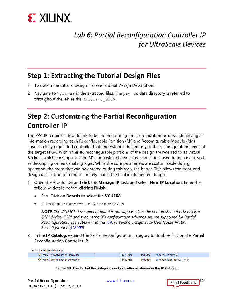
Partial Reconfiguration www.xilinx.com 121 UG947 (v2019.1) June 12, 2019
Lab 6: Partial Reconfiguration Controller IP for UltraScale Devices
Step 1: Extracting the Tutorial Design Files 1. To obtain the tutorial design file, see Tutorial Design Description.
2. Navigate to \prc_us in the extracted files. The prc_us data directory is referred to
throughout the lab as the <Extract_Dir>.
Step 2: Customizing the Partial Reconfiguration Controller IP The PRC IP requires a few details to be entered during the customization process. Identifying all
information regarding each Reconfigurable Partition (RP) and Reconfigurable Module (RM)
creates a fully populated controller that understands the entirety of the reconfiguration needs of
the target FPGA. Within this IP, reconfigurable portions of the design are referred to as Virtual
Sockets, which encompasses the RP along with all associated static logic used to manage it, such
as decoupling or handshaking logic. While the core parameters are customizable during
operation, the more that can be entered during this step, the better. This allows the front-end
design description to more accurately match the final implemented design.
1. Open the Vivado IDE and click the Manage IP task, and select New IP Location. Enter the
following details before clicking Finish:
• Part: Click on Boards to select the VCU108
• IP Location: <Extract_Dir>/Sources/ip
NOTE: The KCU105 development board is not supported, as the boot flash on this board is a
QSPI device. QSPI and sync-mode BPI configuration schemes are not supported for Partial
Reconfiguration. See Table 8-1 in this link of Vivado Design Suite User Guide: Partial
Reconfiguration (UG909).
2. In the IP Catalog, expand the Partial Reconfiguration category to double-click on the Partial
Reconfiguration Controller IP.
Figure 89: The Partial Reconfiguration Controller as shown in the IP Catalog
Send Feedback
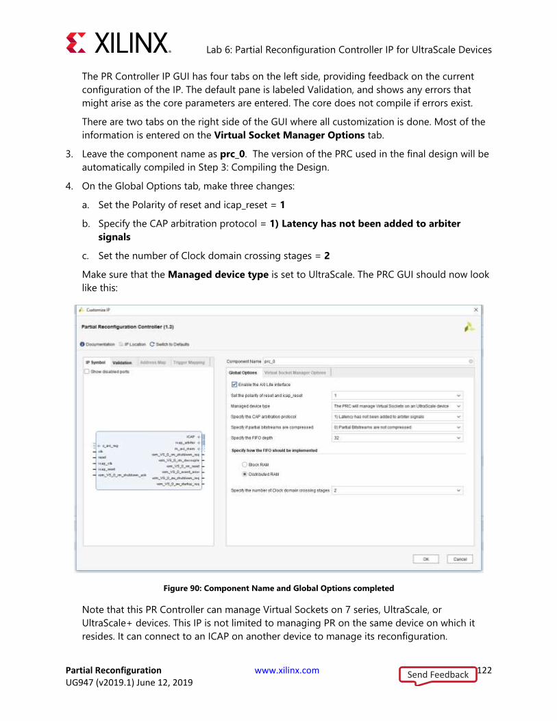
Lab 6: Partial Reconfiguration Controller IP for UltraScale Devices
Partial Reconfiguration www.xilinx.com 122 UG947 (v2019.1) June 12, 2019
The PR Controller IP GUI has four tabs on the left side, providing feedback on the current
configuration of the IP. The default pane is labeled Validation, and shows any errors that
might arise as the core parameters are entered. The core does not compile if errors exist.
There are two tabs on the right side of the GUI where all customization is done. Most of the
information is entered on the Virtual Socket Manager Options tab.
3. Leave the component name as prc_0. The version of the PRC used in the final design will be
automatically compiled in Step 3: Compiling the Design.
4. On the Global Options tab, make three changes:
a. Set the Polarity of reset and icap_reset = 1
b. Specify the CAP arbitration protocol = 1) Latency has not been added to arbiter
signals
c. Set the number of Clock domain crossing stages = 2
Make sure that the Managed device type is set to UltraScale. The PRC GUI should now look
like this:
Figure 90: Component Name and Global Options completed
Note that this PR Controller can manage Virtual Sockets on 7 series, UltraScale, or
UltraScale+ devices. This IP is not limited to managing PR on the same device on which it
resides. It can connect to an ICAP on another device to manage its reconfiguration.
Send Feedback
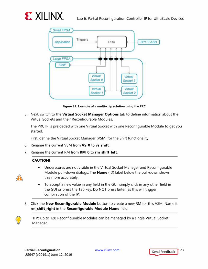
Lab 6: Partial Reconfiguration Controller IP for UltraScale Devices
Partial Reconfiguration www.xilinx.com 123 UG947 (v2019.1) June 12, 2019
Figure 91: Example of a multi-chip solution using the PRC
5. Next, switch to the Virtual Socket Manager Options tab to define information about the
Virtual Sockets and their Reconfigurable Modules.
The PRC IP is preloaded with one Virtual Socket with one Reconfigurable Module to get you
started.
First, define the Virtual Socket Manager (VSM) for the Shift functionality.
6. Rename the current VSM from VS_0 to vs_shift.
7. Rename the current RM from RM_0 to rm_shift_left.
CAUTION!
• Underscores are not visible in the Virtual Socket Manager and Reconfigurable
Module pull-down dialogs. The Name (ID) label below the pull-down shows
this more accurately.
• To accept a new value in any field in the GUI, simply click in any other field in
the GUI or press the Tab key. Do NOT press Enter, as this will trigger
compilation of the IP.
8. Click the New Reconfigurable Module button to create a new RM for this VSM. Name it
rm_shift_right in the Reconfigurable Module Name field.
TIP: Up to 128 Reconfigurable Modules can be managed by a single Virtual Socket
Manager.
Send Feedback

Lab 6: Partial Reconfiguration Controller IP for UltraScale Devices
Partial Reconfiguration www.xilinx.com 124 UG947 (v2019.1) June 12, 2019
9. Configure the vs_shift VSM to have the following properties:
• Has Status Channel = checked
• Has PoR RM = rm_shift_right
• Number of RMs allocated = 4
The PoR RM indicates which RM is contained within the initial full-design configuration file,
so the VSM knows which triggers and events are appropriate upon startup of the FPGA. The
VSM tracks the current active Reconfigurable Module in its socket.
Even through you have only defined two RMs for this Virtual Socket, you have set aside
space for four in total. This allows for expansion later on. Additional Reconfigurable Modules
can be identified using the AXI4-Lite interface, but only if spaces have been reserved for
them.
10. For each of these RMs, enter the following values. Use the Reconfigurable Module to
configure pull-down to switch between the two RMs.
• For rm_shift_left:
o Reset type = Active High
o Duration of Reset = 3
• For rm_shift_right:
o Reset type = Active High
o Duration of Reset = 10
Note: The different reset durations are given to show that these can be independently
assigned, as each RM may have different requirements. Reset durations are measured in
clock cycles.
11. For each RM, assign a bitstream size and location to identify where it will reside in the BPI
flash device.
• For rm_shift_left:
o Bitstream 0 address = 0x00B00000
o Bitstream 0 size (bytes) = 375996
o Bitstream 0 is a clearing bitstream = unchecked
o Bitstream 1 address = 0x00B5C000
o Bitstream 1 size (bytes) = 26036
o Bitstream 1 is a clearing bitstream = checked
Send Feedback

Lab 6: Partial Reconfiguration Controller IP for UltraScale Devices
Partial Reconfiguration www.xilinx.com 125 UG947 (v2019.1) June 12, 2019
• For rm_shift_right:
o Bitstream 0 address = 0x00B62800
o Bitstream 0 size (bytes) = 375996
o Bitstream 0 is a clearing bitstream = unchecked
o Bitstream 1 address = 0x00BBE800
o Bitstream 1 size (bytes) = 26036
o Bitstream 1 is a clearing bitstream = checked
This information is typically not known early in design cycles, as bitstream size is based on
the size and composition of the Reconfigurable Partition Pblock, and bitstream address is
based on storage details. Until the design is to be tested on silicon, these can be set to 0. As
the design settles and hardware testing with the PRC is set to begin, this information can be
added. The bitstream address information must match the information passed during PROM
file generation. Certain bitstream generation options, most notably bitstream compression,
can lead to variations in the final bitstream size for different configurations, even for the
same Reconfigurable Partition.
12. Define the Trigger Options for the Shift functionality:
• Number of Hardware Triggers = 4
• Number of Triggers allocated = 4
The four trigger assignments are done automatically. These can be modified during device
operation using AXI4-Lite, which is especially useful when you have added a new RM
through the same mechanism during a field system upgrade.
At this point, the IP GUI should look like this (showing rm_shift_left here):
Send Feedback
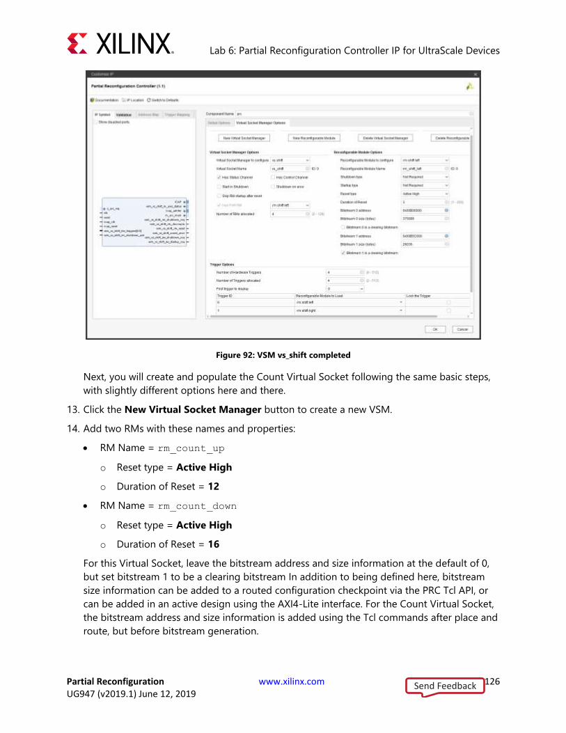
Lab 6: Partial Reconfiguration Controller IP for UltraScale Devices
Partial Reconfiguration www.xilinx.com 126 UG947 (v2019.1) June 12, 2019
Figure 92: VSM vs_shift completed
Next, you will create and populate the Count Virtual Socket following the same basic steps,
with slightly different options here and there.
13. Click the New Virtual Socket Manager button to create a new VSM.
14. Add two RMs with these names and properties:
• RM Name = rm_count_up
o Reset type = Active High
o Duration of Reset = 12
• RM Name = rm_count_down
o Reset type = Active High
o Duration of Reset = 16
For this Virtual Socket, leave the bitstream address and size information at the default of 0,
but set bitstream 1 to be a clearing bitstream In addition to being defined here, bitstream
size information can be added to a routed configuration checkpoint via the PRC Tcl API, or
can be added in an active design using the AXI4-Lite interface. For the Count Virtual Socket,
the bitstream address and size information is added using the Tcl commands after place and
route, but before bitstream generation.
Send Feedback
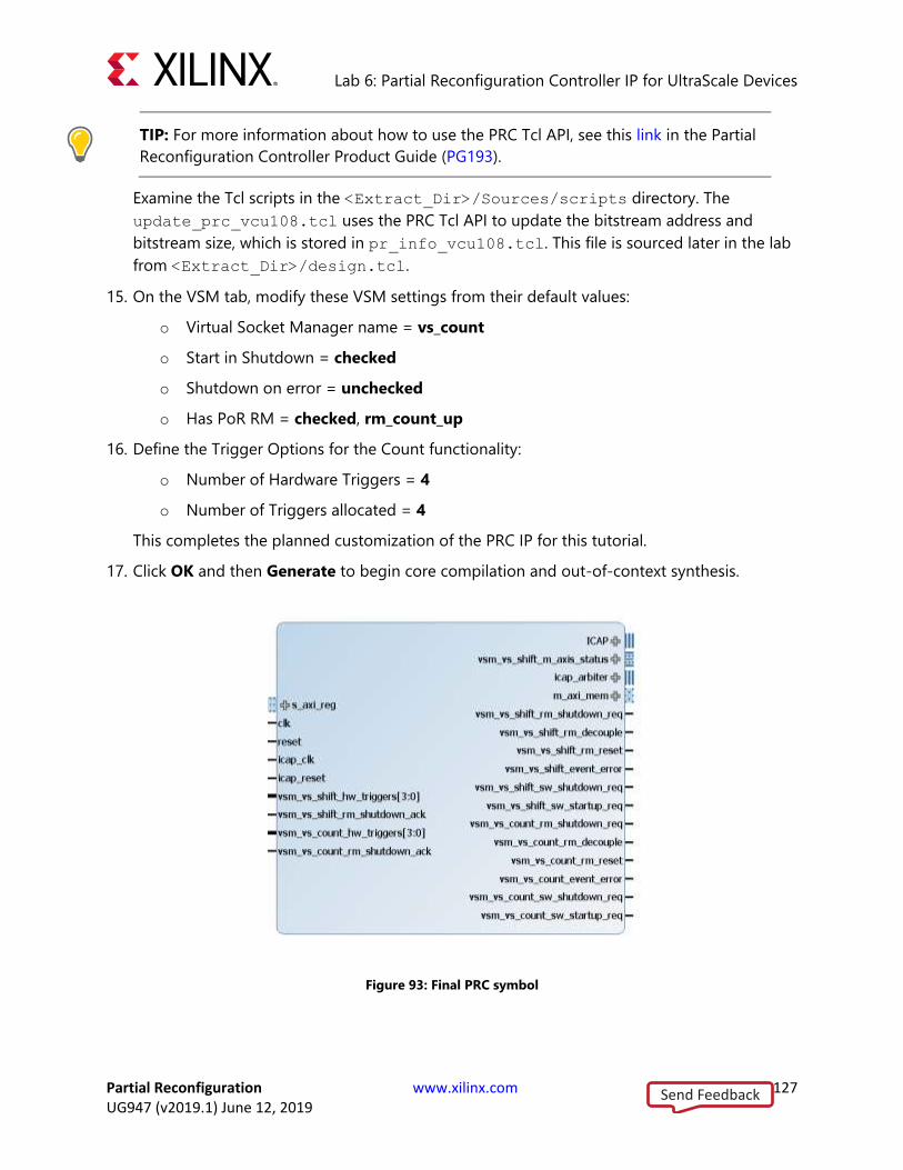
Lab 6: Partial Reconfiguration Controller IP for UltraScale Devices
Partial Reconfiguration www.xilinx.com 127 UG947 (v2019.1) June 12, 2019
TIP: For more information about how to use the PRC Tcl API, see this link in the Partial
Reconfiguration Controller Product Guide (PG193).
Examine the Tcl scripts in the <Extract_Dir>/Sources/scripts directory. The
update_prc_vcu108.tcl uses the PRC Tcl API to update the bitstream address and
bitstream size, which is stored in pr_info_vcu108.tcl. This file is sourced later in the lab
from <Extract_Dir>/design.tcl.
15. On the VSM tab, modify these VSM settings from their default values:
o Virtual Socket Manager name = vs_count
o Start in Shutdown = checked
o Shutdown on error = unchecked
o Has PoR RM = checked, rm_count_up
16. Define the Trigger Options for the Count functionality:
o Number of Hardware Triggers = 4
o Number of Triggers allocated = 4
This completes the planned customization of the PRC IP for this tutorial.
17. Click OK and then Generate to begin core compilation and out-of-context synthesis.
Figure 93: Final PRC symbol
Send Feedback

Lab 6: Partial Reconfiguration Controller IP for UltraScale Devices
Partial Reconfiguration www.xilinx.com 128 UG947 (v2019.1) June 12, 2019
Step 3: Compiling the Design The PR Controller IP is created, but the design is not yet compiled, which could take
approximately an hour. In order to create the PROM image with all the necessary full and partial
images, source the following scripts in Tcl mode using the commands below.
1. vivado -mode tcl -source design.tcl
Sourcing design.tcl generates all the necessary IP (including the PRC), synthesizes and
implements the entire design (three configurations), updates the vs_count VSM using the
PRC Tcl API, and generates bitstreams.
Note that the customization of the IP is scripted. Examine the gen_ip_vcu108.tcl script
(in <Extract_Dir>/Sources/scripts) to see all these parameters defined for
automated IP creation, the PRC, and others. The PRC instance you create using the IP GUI is
not actually used for the full design processing, so you do not have to complete Section 1 to
compile the entire design.
2. vivado -mode tcl -source create_prom_file_vcu108.tcl
Sourcing create_prom_file_vcu108.tcl creates the PROM image for the VCU108
target. This script contains hard-coded values for bitstream address for the entire project. If
this design is modified in such a way that changes bitstream sizes, full or partial, then these
values must also change. Changes that affect bitstream sizes include changing the target
device, changing the size or shape of the Pblocks, or introducing bitstream options such as
compression or per-frame CRC.
This script defines PROM file options by setting properties and then making calls to
write_cfgmem. The PRC works in byte addresses because the data is stored in bytes in AXI.
This linear flash PROM uses half word addresses because it stores data in half words (16
bits). Divide the ROM address by 2 to get the AXI address. For example, the shift_left address
is given as 00B00000 during PRC customization and 00580000 (half that value) for
write_cfgmem. Note that the starting addresses are always multiples of 1024 (0x0400) to
ensure that each bitstream starts on a byte address boundary.
Supplied in the lab directory is a file called prc_bitstream_sizes_lab6.xlsx. In this
file, bitstream sizes are entered by the user based in the yellow highlighted fields. It
calculates the starting address in hex for each partial bitstream at the next byte boundary.
Values in blue are to be supplied for PR Controller IP customization, in either the PRC IP GUI,
in the gen_ip_vcu108.tcl script, or in pr_info_vcu108.tcl which is used for post-
route API modification. The values in green are addresses divided by two to be used in
PROM file generation in the create_prom_file_vcu108.tcl script.
Send Feedback
Lab 6: Partial Reconfiguration Controller IP for UltraScale Devices
Partial Reconfiguration www.xilinx.com 129 UG947 (v2019.1) June 12, 2019
Step 4: Setting up the Board Once the partially reconfigurable design is in operation, you can connect to and communicate
with the core to check status, deliver triggers, and make modifications.
1. Prepare the VCU108 board for programming.
a. Connect the JTAG port (J106) to your computer via the micro-USB connection.
b. Set the configuration mode to 010 (BPI) by setting the Address DIP Switch (SW16) to
00010 (bit 4 is high).
c. Turn on the power to the board.
2. Open the Vivado IDE.
3. Select Flow > Open Hardware Manager
4. Click on the Open Target link and select Auto Connect. The Virtex UltraScale VU095 device
will be recognized.
5. To program the BPI configuration flash, right-click the device (xcvu095_0) and select Add
Configuration Memory Device.
6. From the list shown, select the Micron flash 28f00ag18f and click OK twice.
7. In the Configuration file field, search the tutorial directory for pr_prom.mcs found in the
bitstreams subdirectory. Click OK to select this file, and then click OK to program the flash.
At this point, the board is ready to operate with the tutorial design. Any power-cycle or hard
reset automatically programs the Virtex UltraScale FPGA with this sample design.
Step 5: Operating the Sample Design Position the board so that the text is readable. The LCD screen is on the side closest to you, with
the power connection on the right and the JTAG connection on the left. The buttons of interest
are the five user push buttons in the lower right corner, plus the PROG push button in the
middle right. Their functions are as follows:
• PROG (SW4) – program the device from the BPI flash
• North (SW10) – load the Count Up partial bit file
• South (SW8) – load the Count Down partial bit file
• East (SW9) – load the Shift Right partial bit file
• West (SW6) – load the Shift Left partial bit file
• Center (SW7) – reset the design
Send Feedback

Lab 6: Partial Reconfiguration Controller IP for UltraScale Devices
Partial Reconfiguration www.xilinx.com 130 UG947 (v2019.1) June 12, 2019
Figure 94: Push buttons, switches and connections on the VCU108 demonstration board
1. Program the FPGA by pressing the PROG pushbutton. The 8 GPIO LEDs in the upper-right
corner will start operation after the DONE LED goes high.
At this point, the four bits on the left of the GPIO bank are counting up, and the four bits on
the right are shifting to the right.
2. Press the Shift Left and Shift Right buttons alternately.
With each push, a partial bit file is pulled from the BPI flash by the PRC and delivered to the
ICAP, changing the functionality in that Reconfigurable Partition. When this happens, the
LED shift direction changes, depending on the button pushed.
3. Press the Count Down and Count Up buttons alternately.
With each push, nothing happens. When configuring the PR Controller, the Counter Virtual
Socket was programmed to begin in Shutdown mode. It does not respond to any hardware
or software triggers until it is moved to Active mode.
Step 6: Querying the PRC in the FPGA In this step, you interact with the core via JTAG from the Hardware Manager to understand the
status of the core and issue software triggers.
In the Vivado Hardware Manager, you might need to select Refresh Device to establish the link
to the device over the JTAG connection. Notice the XADC as well as 6 ILA cores and the hw_axi
link shown under the device in the Hardware view.
Send Feedback

Lab 6: Partial Reconfiguration Controller IP for UltraScale Devices
Partial Reconfiguration www.xilinx.com 131 UG947 (v2019.1) June 12, 2019
1. In the Tcl Console, cd into the PRC tutorial directory then source the AXI4-Lite command Tcl
script.
source ./Sources/scripts/axi_lite_procs_us.tcl
This enables a set of procedures that make the subsequent interaction with the PRC easier.
Examine this file to see how these procedures are defined. Note that these are written
explicitly (hard-coded) for this design, the references to Virtual Sockets in any other design
will need to be modified. For more information on this topic, consult the Partial
Reconfiguration Controller Product Guide (PG193).
2. Source the procedure to establish communication with the PRC.
prc_jtag_setup
3. Check the state of each Virtual Socket to see if they are in Shutdown or not.
is_vsm_in_shutdown vs_shift
is_vsm_in_shutdown vs_count
You should see that the Shift Virtual Socket is in Active mode (value = 0), and the Count
Virtual Socket is in Shutdown mode (value = 1).
4. Examine the status of each Virtual Socket.
prc_decode_status vs_shift
prc_decode_status vs_count
Before examining the data returned, reference Table 2-4 in this link of the Partial
Reconfiguration Controller Product Guide (PG193). The table in that section defines the
values in the STATUS register. While this is a 32-bit register, you only need to pay attention
to the lowest 24 bits, as the upper 8 bits are used for Virtual Socket Managers (VSM) in
UltraScale devices.
The status of vs_shift is 263, which is 0000_0000_0000_0001_0000_0111 in binary.
The status for vs_shift may also be 7, where the only difference is that RM_ID is now 0.
o RM_ID (bits 23:8) = 1. This means RM 1 is loaded (rm_shift_right). It may also
appear as RM_ID (bits 24:8) = 0. This means RM 0 is loaded (rm_shift_left).
o SHUTDOWN (bit 7) = 0. This VSM is not in the shutdown state.
o ERROR (bits 6:3) = 0000. There are no errors.
o STATE (bits 2:0) = 111. The Virtual Socket is full.
The status of vs_count is 129, which is 0000_0000_0000_0000_1000_0001 in binary.
o RM_ID (bits 23:8) = 0. This means RM 0 is loaded (rm_count_up).
o SHUTDOWN (bit 7) = 1. This VSM is in the shutdown state.
o ERROR (bits 6:3) = 0000. There are no errors.
o STATE (bits 2:0) = 001. RM_SHUTDOWN_ACK is 1, as this VSM is executing the
hardware shutdown step.
Send Feedback

Lab 6: Partial Reconfiguration Controller IP for UltraScale Devices
Partial Reconfiguration www.xilinx.com 132 UG947 (v2019.1) June 12, 2019
These explicit details are reported in the breakdown of the status register in the return value
from this Tcl proc.
5. Send a software trigger to the Shift Virtual Socket.
prc_send_sw_trigger vs_shift 0
prc_send_sw_trigger vs_shift 1
Remember that values of 0 and 2 correspond to shift left, and values of 1 and 3 correspond
to shift right, as defined during PRC customization.
6. Check the configurations of the RMs for the Count Virtual Socket.
prc_show_rm_configuration vs_count 0
prc_show_rm_configuration vs_count 1
The values for the bitstream sizes and address are reported here. These values could then be
modified to account for necessary adjustments to the size or location of the bitstream.
Different indices can be added to insert new RMs. Note that this query cannot be done for
vs_shift, as the vs_shift VSM is not in the shutdown state.
7. Move the Count Virtual Socket Manager into active mode.
prc_restart_vsm_no_status vs_count
The Count Up and Count Down pushbuttons can now be used to load these partial
bitstreams using the PR Controller.
Step 7: Modifying the PRC in the FPGA In the final step, you add a new Reconfigurable Module to the Shifter VSM. In the
create_prom.tcl script, you can see that two black box modules have already been
generated. These represent two new RMs that may have been created after the static design was
deployed to the field. You modify the PRC settings to access one of these RMs by assigning the
size, address, properties and trigger conditions.
1. Shut down the Shift VSM so it can be modified.
prc_shutdown_vsm vs_shift
2. Check the status of the first three RM IDs to see their register bank assignments.
prc_show_rm_configuration vs_shift 0
prc_show_rm_configuration vs_shift 1
prc_show_rm_configuration vs_shift 2
Currently, RM ID 2 has the same mapping as the partial bit file for RM ID 0, so the same shift
left partial bitstream would be loaded. This is the behavior as requested when the initial
trigger mapping was done during core customization.
3. When the MCS file is created for the prom, it adds additional blanking RMs that are already
loaded into the BPI flash. Use this sequence of commands to reassign the trigger mapping
for slot 2 to point to the blanking Reconfigurable Module for vs_shift.
prc_write_register vs_shift_rm_control2 0
Send Feedback

Lab 6: Partial Reconfiguration Controller IP for UltraScale Devices
Partial Reconfiguration www.xilinx.com 133 UG947 (v2019.1) June 12, 2019
This defines the settings for the RM_CONTROL register for slot 2. No shutdown, startup, or
reset are required. Note how for the other two slots, the differing reset durations lead to
different control values.
prc_write_register vs_shift_rm_bs_index2 327684
This assigns a new bitstream reference for this RM ID.
prc_write_register vs_shift_trigger2 2
This assigns the trigger mapping such that trigger index 2 retrieves RM 2. The
RM_BS_INDEX register within the PR Controller is 32 bits but is broken into two fields.
UltraScale devices require clearing and partial bitstreams. These bitstreams are identified
separately with unique IDs, but referenced together in this field.
This value of 327684 converts to 0000000000000101_0000000000000100 in binary. Or more
simply, ID 5 for the upper 16 bits for the CLEAR_BS_INDEX and ID 4 for the lower 16 bits
for the BS_INDEX. This assignment sets the clearing and partial bitstream identifiers at the
same time.
prc_show_rm_configuration vs_shift 2
This shows the current state of RM ID 2. Note the changes from the prior call to this
command.
4. Complete the RM ID 2 customization by setting the bitstream details.
prc_write_register vs_shift_bs_size4 375996
prc_write_register vs_shift_bs_address4 12935168
prc_write_register vs_shift_bs_size5 26036
prc_write_register vs_shift_bs_address5 13312000
5. Restart the VSM and then issue trigger events to it using software, as there is no pushbutton
assigned for slot 2.
prc_restart_vsm_no_status vs_shift
prc_send_sw_trigger vs_shift 2
Switch between values of 0, 1 and 2 to reload different partial bitstreams.
Note that this same sequence of events could not be performed for the Count VSM as it is
currently configured, even knowing that the PROM image has a Count black box partial
bitstream sitting at address 13338624 with a size of 274104. During PRC customization, this VSM
was selected to have only 2 RMs allocated, so expansion is not permitted.
Send Feedback

Lab 6: Partial Reconfiguration Controller IP for UltraScale Devices
Partial Reconfiguration www.xilinx.com 134 UG947 (v2019.1) June 12, 2019
Conclusion This concludes lab 6. In this lab, you:
• Customized the Partial Reconfiguration Controller IP.
• Created Virtual Sockets and added RMs to them.
• Compiled the design and created a PROM file.
• Programmed the linear flash on the VCU108 board.
• Used pushbuttons to issue hardware triggers.
• Used the AXI-Lite interface to check the core status and issue software triggers.
• Added a new RM to an already deployed design.
Send Feedback
Partial Reconfiguration www.xilinx.com 135 UG947 (v2019.1) June 12, 2019
Lab 7: Partial Reconfiguration Controller IP for UltraScale+ Devices
Overview This lab covers the details of a demonstration that targets the KCU116 or VCU118 demo board.
It is a modified version of the design used in Lab 6: Partial Reconfiguration Controller IP for
UltraScale Devices and is enhanced with these features:
• Software-driven triggering and bitstream management via MicroBlaze
• Partial bitstream delivery from QSPI or DDR4 memory
• Compatibility with Soft Error Mitigation (SEM) IP
• Per-frame CRC checking
• Additional debug capabilities
It retains the PR Controller and PR Decoupler IP from the base design as well.
Note that the VCU118 must be version 2.0 (or newer) with the dual quad SPI flash. Version 1.x
and earlier boards have Micron MT28G BPI flash which is being discontinued.
Step 1: Extracting the Tutorial Design Files 1. To obtain the tutorial design file, see Tutorial Design Description.
2. Navigate to \prc_usp in the extracted files. The prc_usp data directory is referred to
throughout the lab as the <Extract_Dir>.
Step 2: Processing the Tutorial Design The purpose of this design is the end run-time functionality and software management, not
design processing, so the details of the implementation flow are not extensively covered here.
For a review of the Partial Reconfiguration design flow, refer to earlier labs in this document.
1. Extract the tutorial design archive.
2. From a command shell, launch Vivado with the example design project creation script. This
must be launched from the top level of the design archive where this script is located.
vivado –mode tcl –source project_prc_kcu116.tcl
or
vivado –mode tcl –source project_prc_vcu118.tcl
Send Feedback
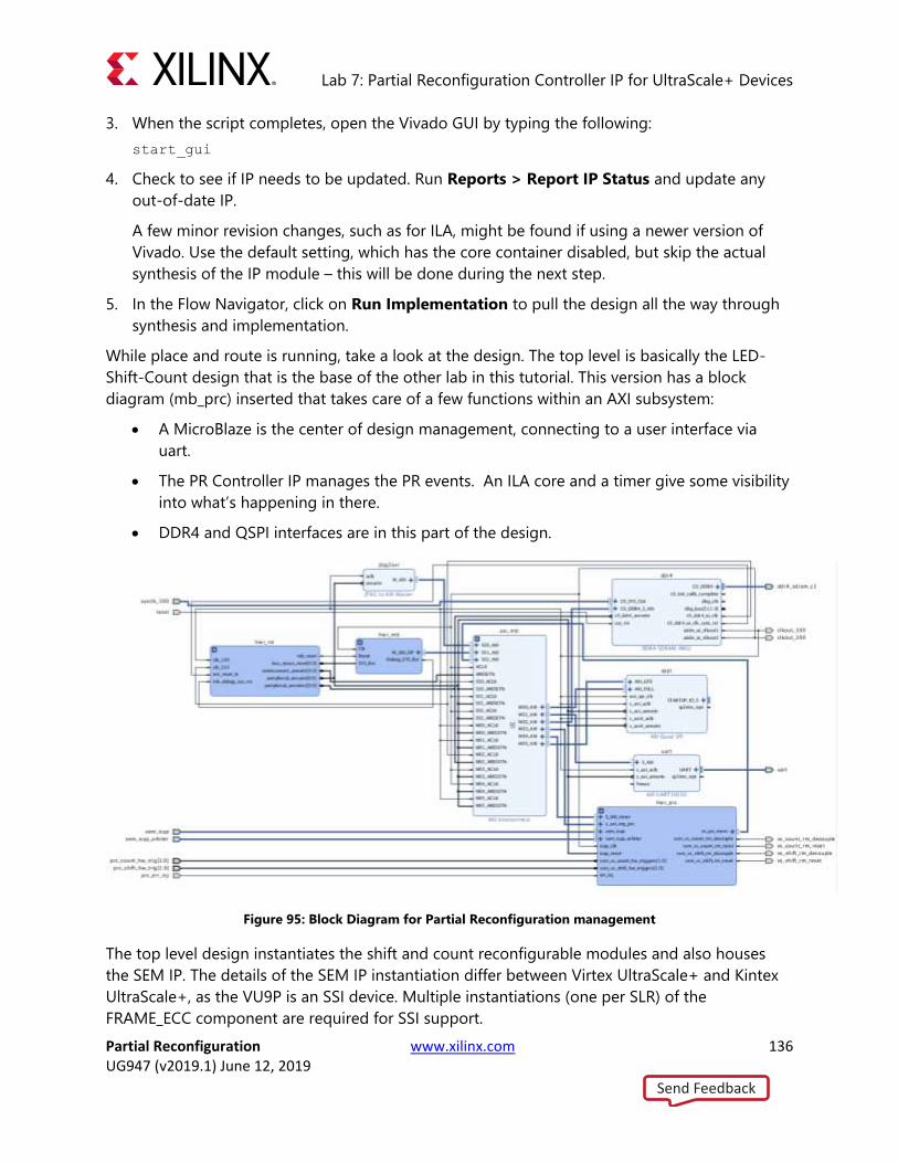
Lab 7: Partial Reconfiguration Controller IP for UltraScale+ Devices
Partial Reconfiguration www.xilinx.com 136 UG947 (v2019.1) June 12, 2019
3. When the script completes, open the Vivado GUI by typing the following:
start_gui
4. Check to see if IP needs to be updated. Run Reports > Report IP Status and update any
out-of-date IP.
A few minor revision changes, such as for ILA, might be found if using a newer version of
Vivado. Use the default setting, which has the core container disabled, but skip the actual
synthesis of the IP module – this will be done during the next step.
5. In the Flow Navigator, click on Run Implementation to pull the design all the way through
synthesis and implementation.
While place and route is running, take a look at the design. The top level is basically the LED-
Shift-Count design that is the base of the other lab in this tutorial. This version has a block
diagram (mb_prc) inserted that takes care of a few functions within an AXI subsystem:
• A MicroBlaze is the center of design management, connecting to a user interface via
uart.
• The PR Controller IP manages the PR events. An ILA core and a timer give some visibility
into what’s happening in there.
• DDR4 and QSPI interfaces are in this part of the design.
Figure 95: Block Diagram for Partial Reconfiguration management
The top level design instantiates the shift and count reconfigurable modules and also houses
the SEM IP. The details of the SEM IP instantiation differ between Virtex UltraScale+ and Kintex
UltraScale+, as the VU9P is an SSI device. Multiple instantiations (one per SLR) of the
FRAME_ECC component are required for SSI support.
Send Feedback
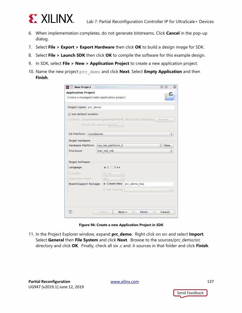
Lab 7: Partial Reconfiguration Controller IP for UltraScale+ Devices
Partial Reconfiguration www.xilinx.com 137 UG947 (v2019.1) June 12, 2019
6. When implementation completes, do not generate bitstreams. Click Cancel in the pop-up
dialog.
7. Select File > Export > Export Hardware then click OK to build a design image for SDK.
8. Select File > Launch SDK then click OK to compile the software for this example design.
9. In SDK, select File > New > Application Project to create a new application project.
10. Name the new project prc_demo and click Next. Select Empty Application and then
Finish.
Figure 96: Create a new Application Project in SDK
11. In the Project Explorer window, expand prc_demo. Right click on src and select Import.
Select General then File System and click Next. Browse to the sources/prc_demo/src
directory and click OK. Finally, check all six .c and .h sources in that folder and click Finish.
Send Feedback
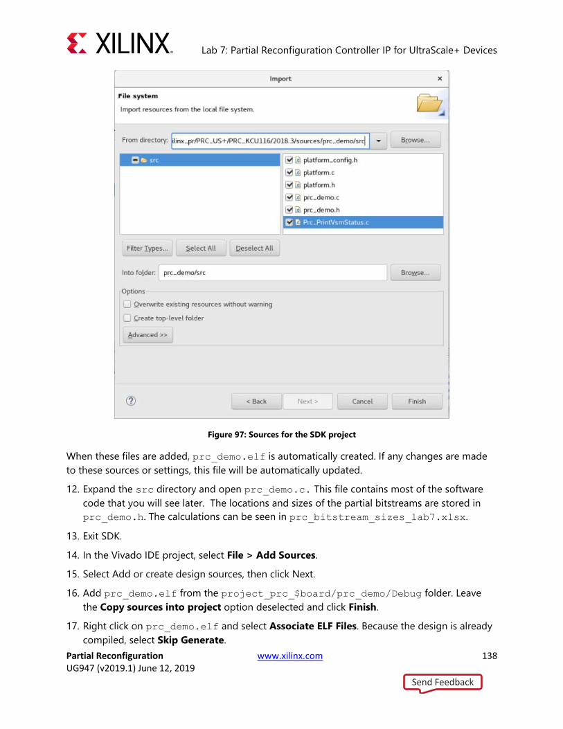
Lab 7: Partial Reconfiguration Controller IP for UltraScale+ Devices
Partial Reconfiguration www.xilinx.com 138 UG947 (v2019.1) June 12, 2019
Figure 97: Sources for the SDK project
When these files are added, prc_demo.elf is automatically created. If any changes are made
to these sources or settings, this file will be automatically updated.
12. Expand the src directory and open prc_demo.c. This file contains most of the software
code that you will see later. The locations and sizes of the partial bitstreams are stored in
prc_demo.h. The calculations can be seen in prc_bitstream_sizes_lab7.xlsx.
13. Exit SDK.
14. In the Vivado IDE project, select File > Add Sources.
15. Select Add or create design sources, then click Next.
16. Add prc_demo.elf from the project_prc_$board/prc_demo/Debug folder. Leave
the Copy sources into project option deselected and click Finish.
17. Right click on prc_demo.elf and select Associate ELF Files. Because the design is already
compiled, select Skip Generate.
Send Feedback

Lab 7: Partial Reconfiguration Controller IP for UltraScale+ Devices
Partial Reconfiguration www.xilinx.com 139 UG947 (v2019.1) June 12, 2019
18. In the window that appears, change the top reference for Design Sources to the
prc_demo.elf file that was just added. Then click OK.
Figure 98: Associate the prc_demo.elf file with the MicroBlaze instance
19. Right click on impl_1 and select Generate Bitstream.
This action creates the full bitstream (containing the MicroBlaze code in the .elf file) for the
Shift Right – Count Up configuration, along with partial bitstreams for each of the
Reconfigurable Modules. Only the full configuration bitstream from the parent run will be
used here, so there is no need to generate bitstreams from the child_0_impl_1 run. Note that
the sizes for all partial bitstreams are reported, in bits, in the log.
20. Source this script to create all bit files. In the Tcl Console, make sure you are currently in the
level above the project_prc_<board> directory, where this script exists.
source create_all_bitstreams_kcu116.tcl
or
source create_all_bitstreams_vcu118.tcl
Settings for full versus partial bitstreams must be different to account for the configuration
modes and options in this design. This is done within a Tcl script that copies the full
bitstream created in the prior step, and then creates all the partial bitstreams that are
necessary for all Reconfigurable Modules.
Send Feedback
Lab 7: Partial Reconfiguration Controller IP for UltraScale+ Devices
Partial Reconfiguration www.xilinx.com 140 UG947 (v2019.1) June 12, 2019
Important: Users are not yet able to set different options for full versus partial bitstreams
in project mode in the Vivado IDE. This feature is planned for a future Vivado release and
is expected to be shown as a new page in the Partial Reconfiguration Wizard.
Examining this script shows that the CONFIG_MODE must change from the default of SPIx4 for
the initial configuration to SELECTMAP32 for the partial bitstreams, which are delivered to the
ICAP. Two versions of partial bitstreams are generated, with and without the per-frame CRC
feature enabled.
21. Source one of these two scripts to create PROM images for the target board.
source create_prom_file_kcu116.tcl
or
source create_prom_file_vcu118.tcl
This creates a QSPI boot image with the full bitstream followed by all the partial bitstreams. The
addresses listed in this script are calculated based on the size of each partial bitstream. Note
that the sizes for all partial bitstreams are reported, in bytes, in the log. The calculations can be
seen in prc_bitstream_sizes_lab7.xlsx.
Step 3: Running the Tutorial Design Once all the bitstreams and prom images have been created, you can run the design on
hardware. There are a number of different features that can be demonstrate. There is no specific
order in which these demonstrations must be done after the device has been programmed.
Program the QSPI Flash Device
1. Connect the target board to your computer and power the board on. Connect to both
micro-USB ports for JTAG and UART connections.
2. Program the configuration memory device (QSPI).
a. Open the Vivado Hardware Manager and connect to the target board.
b. Right click on the device and select Add Configuration Memory Device
c. Select the Micron mt25qu01g that supports x1, x2 and x4 modes.
Send Feedback
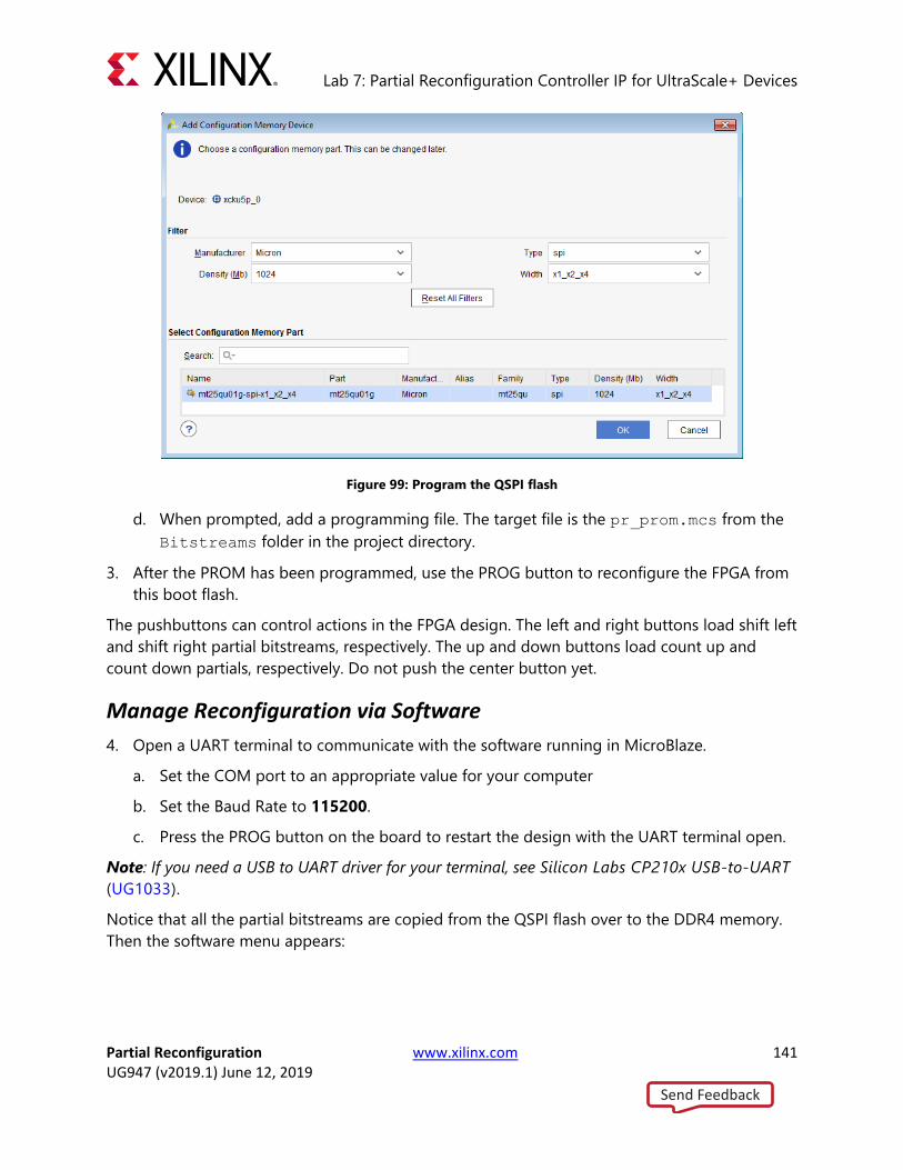
Lab 7: Partial Reconfiguration Controller IP for UltraScale+ Devices
Partial Reconfiguration www.xilinx.com 141 UG947 (v2019.1) June 12, 2019
Figure 99: Program the QSPI flash
d. When prompted, add a programming file. The target file is the pr_prom.mcs from the
Bitstreams folder in the project directory.
3. After the PROM has been programmed, use the PROG button to reconfigure the FPGA from
this boot flash.
The pushbuttons can control actions in the FPGA design. The left and right buttons load shift left
and shift right partial bitstreams, respectively. The up and down buttons load count up and
count down partials, respectively. Do not push the center button yet.
Manage Reconfiguration via Software
4. Open a UART terminal to communicate with the software running in MicroBlaze.
a. Set the COM port to an appropriate value for your computer
b. Set the Baud Rate to 115200.
c. Press the PROG button on the board to restart the design with the UART terminal open.
Note: If you need a USB to UART driver for your terminal, see Silicon Labs CP210x USB-to-UART
(UG1033).
Notice that all the partial bitstreams are copied from the QSPI flash over to the DDR4 memory.
Then the software menu appears:
Send Feedback

Lab 7: Partial Reconfiguration Controller IP for UltraScale+ Devices
Partial Reconfiguration www.xilinx.com 142 UG947 (v2019.1) June 12, 2019
Figure 100: The pr_demo software application running
The menu options allow you to:
• 1-4: These are the four trigger options to load partial bitstreams to the ICAP via the PR
Controller. These mimic the pushbuttons on the board.
• 5-6: These toggle the PR Controller status between active and shutdown mode for both
RPs. When the RPs are in shutdown mode, triggers (software or hardware) are ignored.
• 7: This toggles the partial bitstreams used between standard partials and those
instrumented with per-frame CRC checks.
• 8: This toggles the partial bitstream source between QSPI and DDR4 memory storage.
• 9: Reports the current status of each Virtual Socket.
As you walk through these different features, the software will give feedback. Note that
reconfiguration time is reported each time PR is executed from within the software.
Monitor Partial Reconfiguration via Debug Cores
Vivado debug cores have been inserted in this design, allowing you to monitor activity during
partial reconfiguration events. A key detail for configuring via the ICAP is to have prepared the
partial bitstreams with the right bit and byte ordering for each .bin file.
5. In the Vivado Hardware Manager, refresh the device to find all the Vivado Debug cores.
There are three ILA cores, one VIO core and one MIG core in this design.
Send Feedback
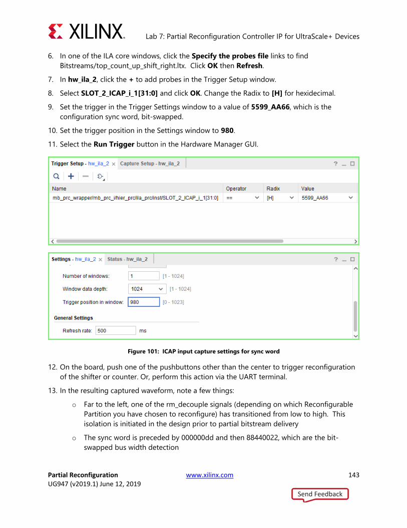
Lab 7: Partial Reconfiguration Controller IP for UltraScale+ Devices
Partial Reconfiguration www.xilinx.com 143 UG947 (v2019.1) June 12, 2019
6. In one of the ILA core windows, click the Specify the probes file links to find
Bitstreams/top_count_up_shift_right.ltx. Click OK then Refresh.
7. In hw_ila_2, click the + to add probes in the Trigger Setup window.
8. Select SLOT_2_ICAP_i_1[31:0] and click OK. Change the Radix to [H] for hexidecimal.
9. Set the trigger in the Trigger Settings window to a value of 5599_AA66, which is the
configuration sync word, bit-swapped.
10. Set the trigger position in the Settings window to 980.
11. Select the Run Trigger button in the Hardware Manager GUI.
Figure 101: ICAP input capture settings for sync word
12. On the board, push one of the pushbuttons other than the center to trigger reconfiguration
of the shifter or counter. Or, perform this action via the UART terminal.
13. In the resulting captured waveform, note a few things:
o Far to the left, one of the rm_decouple signals (depending on which Reconfigurable
Partition you have chosen to reconfigure) has transitioned from low to high. This
isolation is initiated in the design prior to partial bitstream delivery
o The sync word is preceded by 000000dd and then 88440022, which are the bit-
swapped bus width detection
Send Feedback
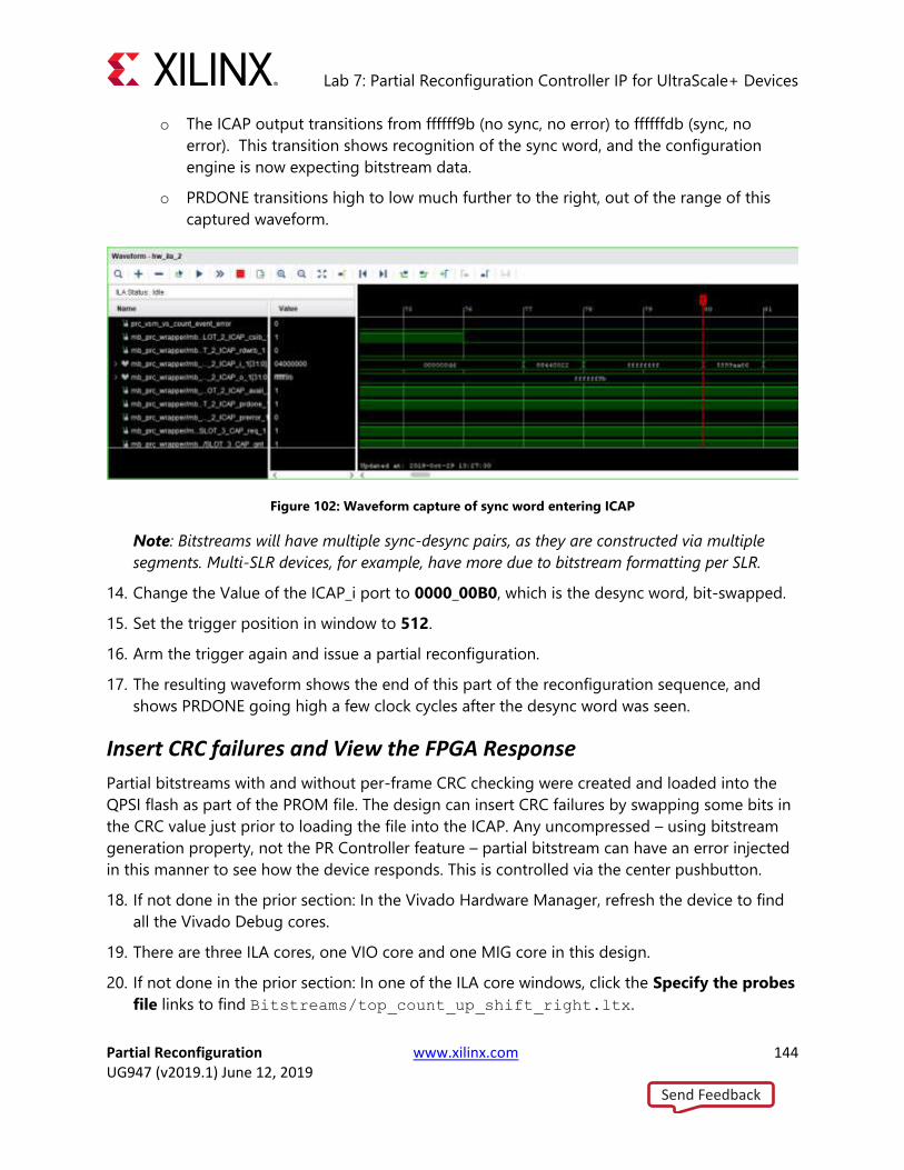
Lab 7: Partial Reconfiguration Controller IP for UltraScale+ Devices
Partial Reconfiguration www.xilinx.com 144 UG947 (v2019.1) June 12, 2019
o The ICAP output transitions from ffffff9b (no sync, no error) to ffffffdb (sync, no
error). This transition shows recognition of the sync word, and the configuration
engine is now expecting bitstream data.
o PRDONE transitions high to low much further to the right, out of the range of this
captured waveform.
Figure 102: Waveform capture of sync word entering ICAP
Note: Bitstreams will have multiple sync-desync pairs, as they are constructed via multiple
segments. Multi-SLR devices, for example, have more due to bitstream formatting per SLR.
14. Change the Value of the ICAP_i port to 0000_00B0, which is the desync word, bit-swapped.
15. Set the trigger position in window to 512.
16. Arm the trigger again and issue a partial reconfiguration.
17. The resulting waveform shows the end of this part of the reconfiguration sequence, and
shows PRDONE going high a few clock cycles after the desync word was seen.
Insert CRC failures and View the FPGA Response
Partial bitstreams with and without per-frame CRC checking were created and loaded into the
QPSI flash as part of the PROM file. The design can insert CRC failures by swapping some bits in
the CRC value just prior to loading the file into the ICAP. Any uncompressed – using bitstream
generation property, not the PR Controller feature – partial bitstream can have an error injected
in this manner to see how the device responds. This is controlled via the center pushbutton.
18. If not done in the prior section: In the Vivado Hardware Manager, refresh the device to find
all the Vivado Debug cores.
19. There are three ILA cores, one VIO core and one MIG core in this design.
20. If not done in the prior section: In one of the ILA core windows, click the Specify the probes
file links to find Bitstreams/top_count_up_shift_right.ltx.
Send Feedback

Lab 7: Partial Reconfiguration Controller IP for UltraScale+ Devices
Partial Reconfiguration www.xilinx.com 145 UG947 (v2019.1) June 12, 2019
21. Click OK then Refresh.
22. In hw_ila_2, click the + to add probes in the Trigger Setup window.
23. Select icap_err_inserted and click OK.
24. Set the trigger in the Trigger Settings window to rising edge of icap_error_inserted.
25. Set the trigger position in the Settings window to 512.
26. Push the Run Trigger button in Hardware Manager GUI.
Figure 103: Trigger setting for icap_err_inserted
27. In the UART terminal, set Reconfig Type as Normal CRC from DDR4. This is the default
setting.
Send Feedback

Lab 7: Partial Reconfiguration Controller IP for UltraScale+ Devices
Partial Reconfiguration www.xilinx.com 146 UG947 (v2019.1) June 12, 2019
Figure 104: Design ready to reconfigure from DDR4 without inserted CRC
28. Push the center pushbutton, and then reconfigure the module you’d like via pushbutton or
the UART terminal. The CRC value at the end of the partial bitstream is swapped to cause a
CRC error. As a result, INIT_B goes low (the INIT_B LED turns red), indicating a CRC error.
Note: On the KCU116 board, the INIT_B LED is on the underside of the board.
29. In ILA Waveform, the trigger location marks where icap_err_inserted is asserted. After the
error insertion, you will see PRERROR then PRDONE goes high. Also, the rm_decouple signal
is high throughout, indicating the Reconfigurable Partition is still isolated.
Figure 105: Waveform capture showing icap_err_inserted, PRERROR, PRDONE, and decouple asserted
Note: The prc_vsm_vs_*_event_error signal is low in this waveform, but it will be pulsed outside
of captured waveform because of the latency in PR Controller.
If the CRC error is found using the standard CRC, which only occurs at the end of the partial
bitstream, the incorrect bitstream has already been loaded into the device. There is no way
to know where any incorrect bits exist, or if they will disrupt the reconfigurable or static
design. The only way to be sure of a full recovery from this condition is to perform a full
reconfiguration of the device. In this tutorial, only the CRC value is swapped, so we can be
assured that the error has not affected the static design.
Send Feedback

Lab 7: Partial Reconfiguration Controller IP for UltraScale+ Devices
Partial Reconfiguration www.xilinx.com 147 UG947 (v2019.1) June 12, 2019
30. When CRC error occurred, the PR Controller entered shutdown mode. In the UART terminal,
Report Status (option 9) shows the RP is in shutdown mode and it reports a BS ERROR. To
recover from this error status, return the RP to active mode by selecting Put RPs in Active
Mode (option 5) from the terminal, and reconfigure with a correct partial bit file. Then INIT_B
returns high (LED turns green) and the design is now back to normal operation.
Next, try with per-frame CRC values inserted.
31. In the terminal, set the Reconfig Type to per Frame CRC (option 7).
32. In the Hardware Manager, re-arm the trigger by clicking the Run Trigger button. Then
perform partial reconfiguration from the terminal or via pushbutton
33. In the ILA waveform, you can see the error has been inserted in the first frame of partial
bitstream – you can see partial reconfiguration starts soon after vs_rm_*_decouple goes high.
However, when using per-frame CRC, the error inserted frame has not been loaded into the
device yet, so there is no need for a reconfiguration of the full design, just reconfigure the
incomplete Reconfigurable Partition with a valid partial bitstream. To recover from the error
status, repeat the procedure from step 8.
Conclusion This concludes lab 7. In this lab, you:
• Implemented an UltraScale+ version of a design with the Partial Reconfiguration
Controller.
• Compiled a MicroBlaze core with software that manages partial reconfiguration events.
• Programmed the QSPI on the KCU116 or VCU118 board.
• Used a UART interface to manage partial reconfiguration from QSPI or DDR4 memory.
• Inserted bitstream delivery errors to see CRC checking capabilities.
NOTE: Although an SEM core exists within the design, it is not exercised during hardware
testing in this lab. If the SEM core is running on hardware to detect upset events, it must be
paused before performing partial reconfiguration.
Send Feedback

Partial Reconfiguration www.xilinx.com 148 UG947 (v2019.1) June 12, 2019
Legal Notices
Please Read: Important Legal Notices The information disclosed to you hereunder (the “Materials”) is provided solely for the selection and use of Xilinx
products. To the maximum extent permitted by applicable law: (1) Materials are made available "AS IS" and with all
faults, Xilinx hereby DISCLAIMS ALL WARRANTIES AND CONDITIONS, EXPRESS, IMPLIED, OR STATUTORY,
INCLUDING BUT NOT LIMITED TO WARRANTIES OF MERCHANTABILITY, NON-INFRINGEMENT, OR FITNESS
FOR ANY PARTICULAR PURPOSE; and (2) Xilinx shall not be liable (whether in contract or tort, including
negligence, or under any other theory of liability) for any loss or damage of any kind or nature related to, arising
under, or in connection with, the Materials (including your use of the Materials), including for any direct, indirect,
special, incidental, or consequential loss or damage (including loss of data, profits, goodwill, or any type of loss or
damage suffered as a result of any action brought by a third party) even if such damage or loss was reasonably
foreseeable or Xilinx had been advised of the possibility of the same. Xilinx assumes no obligation to correct any
errors contained in the Materials or to notify you of updates to the Materials or to product specifications. You may not
reproduce, modify, distribute, or publicly display the Materials without prior written consent. Certain products are
subject to the terms and conditions of Xilinx’s limited warranty, please refer to Xilinx’s Terms of Sale which can be
viewed at http://www.xilinx.com/legal.htm#tos; IP cores may be subject to warranty and support terms contained in a
license issued to you by Xilinx. Xilinx products are not designed or intended to be fail-safe or for use in any
application requiring fail-safe performance; you assume sole risk and liability for use of Xilinx products in such critical
applications, please refer to Xilinx’s Terms of Sale which can be viewed at http://www.xilinx.com/legal.htm#tos.
AUTOMOTIVE APPLICATIONS DISCLAIMER
AUTOMOTIVE PRODUCTS (IDENTIFIED AS “XA” IN THE PART NUMBER) ARE NOT WARRANTED FOR USE IN
THE DEPLOYMENT OF AIRBAGS OR FOR USE IN APPLICATIONS THAT AFFECT CONTROL OF A VEHICLE
(“SAFETY APPLICATION”) UNLESS THERE IS A SAFETY CONCEPT OR REDUNDANCY FEATURE
CONSISTENT WITH THE ISO 26262 AUTOMOTIVE SAFETY STANDARD (“SAFETY DESIGN”). CUSTOMER
SHALL, PRIOR TO USING OR DISTRIBUTING ANY SYSTEMS THAT INCORPORATE PRODUCTS,
THOROUGHLY TEST SUCH SYSTEMS FOR SAFETY PURPOSES. USE OF PRODUCTS IN A SAFETY
APPLICATION WITHOUT A SAFETY DESIGN IS FULLY AT THE RISK OF CUSTOMER, SUBJECT ONLY TO
APPLICABLE LAWS AND REGULATIONS GOVERNING LIMITATIONS ON PRODUCT LIABILITY.
© Copyright 2012-2019 Xilinx, Inc. Xilinx, the Xilinx logo, Artix, ISE, Kintex, Spartan, Virtex, Zynq, and other
designated brands included herein are trademarks of Xilinx in the United States and other countries. All other
trademarks are the property of their respective owners.
Send Feedback