201509 · Title: 201509.pdf Author: DAITO-D04 Created Date: 5/16/2020 10:20:57 AM

© Copyright 2012 Xilinx
Announcing Vivado™ Built from the Ground Up for the Next Decade of ‘All Programmable’ Devices

© Copyright 2012 Xilinx
IP & System Centric Next Generation Design Environment
For the Next Decade of ‘All Programmable’ Devices
Accelerating Integration & Implementation up to 4X
Announcing Vivado Design Suite
Built from the Ground Up for the Next Decade
of Programmable Design
Page 3
© Copyright 2012 Xilinx
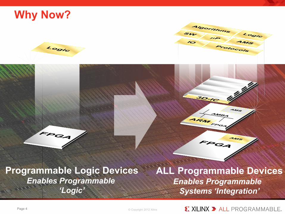
Why Now?
Programmable Logic Devices Enables Programmable
‘Logic’
ALL Programmable Devices Enables Programmable
Systems ‘Integration’
Page 4

© Copyright 2012 Xilinx
Bottlenecks are Shifting
System Integration Bottlenecks – Design and IP reuse – Integrating algorithmic and RTL level IP – Mixing DSP, embedded, connectivity, logic – Verification of blocks and “systems”
Implementation Bottlenecks – Hierarchical chip planning – Multi-domain and multi-die physical optimization – Predictable ‘design’ vs. ‘timing’ closure – Late ECOs and rippling effect of changes
Page 5
© Copyright 2012 Xilinx
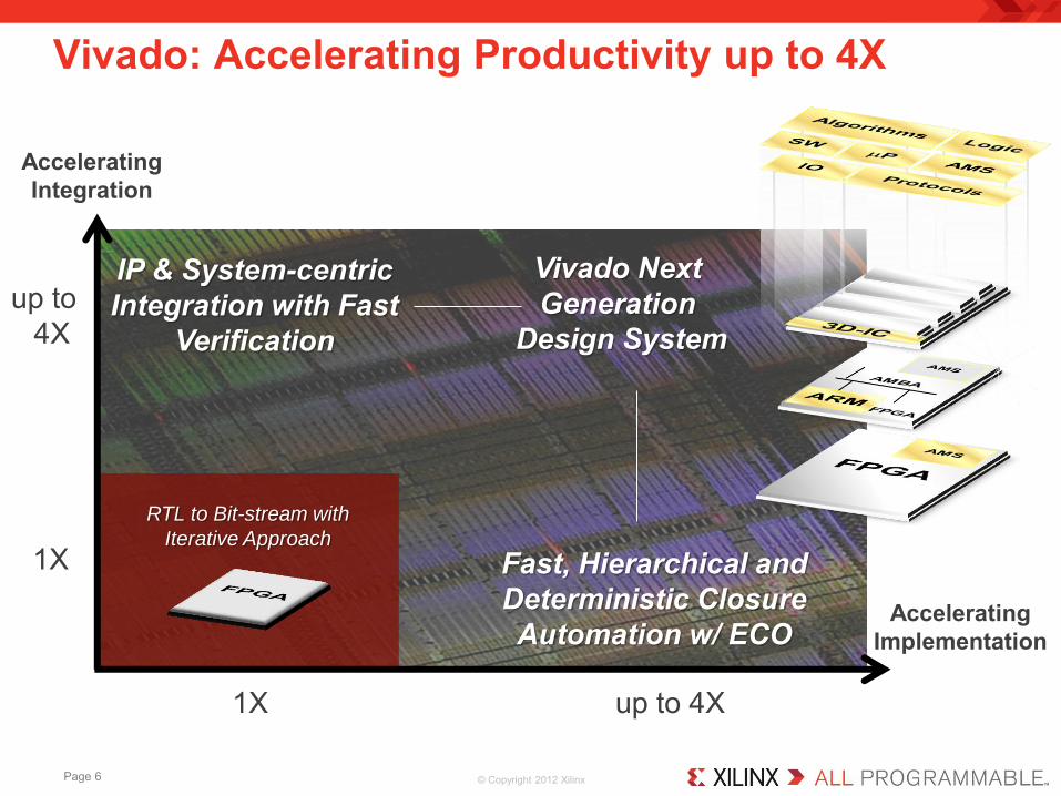
Vivado: Accelerating Productivity up to 4X
Accelerating Integration
Accelerating Implementation
Fast, Hierarchical and Deterministic Closure Automation w/ ECO
IP & System-centric Integration with Fast
Verification
RTL to Bit-stream with
Iterative Approach 1X
1X up to 4X
up to 4X
Vivado Next Generation
Design System
Page 6

© Copyright 2012 Xilinx
Vivado Design Suite Elements
Integrated Design Environment D
ebug and Analysis
Shared Scalable Data M
odel
Fast, Hierarchical and Deterministic Closure Automation w/ ECO
Accelerating Integration
Accelerating Implementation
IP & System-centric Integration with Fast
Verification
Scalable to 100M Gates
Page 7

© Copyright 2012 Xilinx
Shares design information between implementation steps – Ensures fast convergence and timing closure
Highly efficient memory utilization – Scalable to future families > 10M logic cells
(100M Gates)
Enables cross-probing across the entire design
Vivado Key Enabling Technologies Shared, Scalable Data Model
Estimation
IP Integration
RTL Design Synthesis Place & Route
Progressive estimation accuracy across the entire flow
Shared, Scalable Data Model
Reduced iterations late in the cycle
entity FIR is port (clk : in rst : in din : in
Timing Report
Timing Path #1 Timing Path #2 Timing Path #3
RTL Schematics Placement
Reports
Code Changes
Tool Settings
Placement Edits
Page 8

© Copyright 2012 Xilinx
Vivado Design Suite Elements
Integrated Design Environment D
ebug and Analysis
Shared Scalable Data M
odel
Accelerating Integration
IP & System-centric Integration with Fast
Verification IP Assembly
ESL Algorithm IP Synthesis
Systems Integration
Stds Based IP Reuse
Scalable to 100M Gates
Fast Simulation & HW Co-sim
Page 9

© Copyright 2012 Xilinx
IP & System-centric Integration with Fast
Verification IP Assembly
ESL Algorithm IP Synthesis
IP & HW-SW Integrator
Stds Based IP Reuse
Fast Simulation & HW Co-Sim
ISim Vivado
Runtim
e IP-Centric Integration with Fast Verification
w/ HW Co-sim
Tcl SDC
ProcessorSystemPCIe
MemoryInterface
User IP Xilinx IP 3rd Party IP
Display
Processing Datapath
Embedded Interconnect
Memory Interfaces
Hand-coded VHDL
Vivado HLS C
Design Time (weeks)
12 1
Latency (ms)
37 21
Memory (RAMB18E1)
134 (16%) 10 (1%)
Memory (RAMB36E1)
273 (65%) 138 (33%)
Registers 29686 (9%) 14263 (4%)
LUTs 28152 (18%) 24257 (16%)
Page 10

© Copyright 2012 Xilinx
Share IP within your team, project or company 3rd party IP delivered with a common look and feel
Reuse IP at any point in the implementation process – Source, placed, or placed and routed
Package Designs into System-Level IP for Reuse
IP Packager
Source (C, RTL, IP, etc) Simulation Models
Documentation Example Designs
Test Bench
ProcessorSystemPCIe
MemoryInterface
User IP Xilinx IP 3rd Party IP
Display
Processing Datapath
Embedded Interconnect
Memory Interfaces
Vivado IP Integrator
Standardized IP-XACT representation
Xilinx IP
3rd Party IP
User IP
Reuse in different designs
Reuse multiple times
Page 11

© Copyright 2012 Xilinx
Integrated IP catalog – Powerful search capabilities – Single-click access to IP functionality
and collateral
IP customization and generation – Instant access to customization GUI – Generate output products in
project or remote directory – Customize graphically or via Tcl
Seamless IP Access and Customization
Page 12
© Copyright 2012 Xilinx
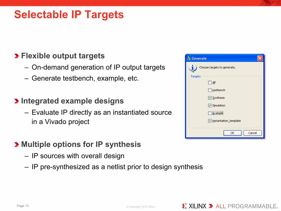
Flexible output targets – On-demand generation of IP output targets – Generate testbench, example, etc.
Integrated example designs – Evaluate IP directly as an instantiated source
in a Vivado project
Multiple options for IP synthesis – IP sources with overall design – IP pre-synthesized as a netlist prior to design synthesis
Selectable IP Targets
Page 13

© Copyright 2012 Xilinx
IEEE 1685 IP-XACT is an industry standard way to represent data about IP (meta-data) – Port information – Latency – Configurable parameters – Etc.
ASCII XML based Enables IP to be used in multiple vendor tools flows
IP Packager: IP-XACT
Page 14
© Copyright 2012 Xilinx
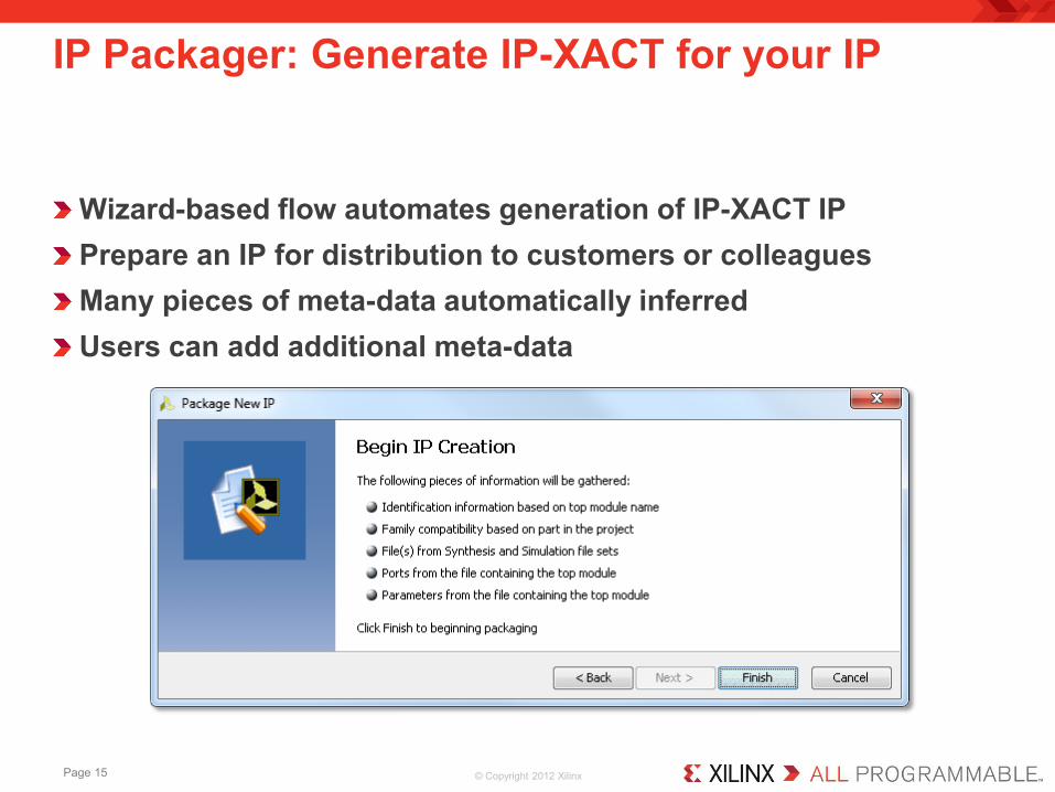
Wizard-based flow automates generation of IP-XACT IP Prepare an IP for distribution to customers or colleagues Many pieces of meta-data automatically inferred Users can add additional meta-data
IP Packager: Generate IP-XACT for your IP
Page 15

© Copyright 2012 Xilinx
1. Run IP Packager from Tools menu 2. Package sources from Vivado project as IP 3. Provide information to uniquely identify your IP
IP Packager: Create System-Level IP
Page 16

© Copyright 2012 Xilinx
1. Unzip IP to a local directory 2. Right-click on IP Catalog 3. Add directory to IP Catalog
Extensible IP Catalog: Add Packaged IP
Page 17

© Copyright 2012 Xilinx
A graphical design environment to enable rapid and accurate connection of complex IP – Connections made at the interface level, not the individual signal level – Automatic setting and propagation of IP parameters – Automated generated of RTL – Full support for arbitrary levels of design hierarchy – Capable of processor-based or non-processor based design creation
Tight integration with Vivado IP Packager flow for rapid IP and subsystem reuse
Vivado IP Integrator
Page 18

© Copyright 2012 Xilinx
IP Integrator User Interface
System Hierarchy View
TCL Console
Interface Connections with Real-time DRCs
Hierarchy Support
Page 19

© Copyright 2012 Xilinx
IP and system configuration rules can be very complex – User will require help to correctly connect IPs
IP Integrator provides immediate feedback on design errors/optimization
IP Integrator Real-time DRCs
Page 20

© Copyright 2012 Xilinx
All IP Integrator automation services can issue DRCs from: – IP configuration XGUI – Built-in automation services
Not just errors: Intelligent DRCs may also include solutions – Goal: Proposed solutions can be actual Tcl code, not just passive text
GUI collects, prioritize and reports DRCs to the user so they can make informed choices
IP Integrator Real-time DRCs (cont)
Apply solution 1
– IP specific automation services – System optimization services
Page 21

© Copyright 2012 Xilinx
Graphical design to enable rapid and accurate connection of complex IP
– Connections made at the interface level, not the individual signal level
– Automatic setting and propagation of IP parameters
– Automated generation of RTL – Full support for arbitrary levels of design
hierarchy – Capable of processor-based or non-processor
based design creation
Tight integration with Vivado IP Packager flow for rapid IP and subsystem reuse
Vivado IP Integrator – Demo
Start Demo >
ProcessorSystemPCIe
MemoryInterface
User IP Xilinx IP 3rd Party IP
Display
Processing Datapath
Embedded Interconnect
Memory Interfaces
Page 22

© Copyright 2012 Xilinx
Ideal for DSP, video and high performance compute applications QoR that rivals hand coded RTL
– Fast compilation and design exploration
– Algorithm/architecture feasibility
Comprehensive coverage – C/C++/SystemC – Arbitrary precision – Floating-point
Accelerated verification – 2 to 3 orders of magnitude faster than
RTL for larger design
Vivado High-Level Synthesis Accelerates IP Development and Design Space Exploration
BDTI certified and production proven at 20+ customer sites
Page 23
© Copyright 2012 Xilinx
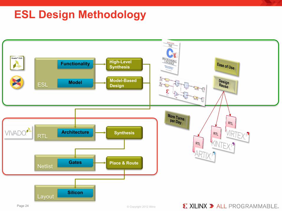
ESL Design Methodology
ESL
Functionality
Netlist Gates
Layout Silicon
High-Level Synthesis
Synthesis
Place & Route
RTL Architecture
Model-Based Design
Model
Page 24
© Copyright 2012 Xilinx
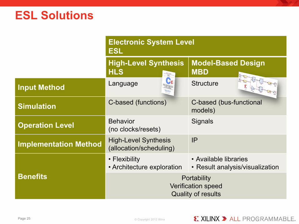
Electronic System Level ESL High-Level Synthesis HLS
Model-Based Design MBD
Input Method Language
Structure
Simulation C-based (functions) C-based (bus-functional models)
Operation Level Behavior (no clocks/resets)
Signals
Implementation Method High-Level Synthesis (allocation/scheduling)
IP
Benefits
• Flexibility • Architecture exploration
• Available libraries • Result analysis/visualization
Portability Verification speed Quality of results
ESL Solutions
Page 25
© Copyright 2012 Xilinx
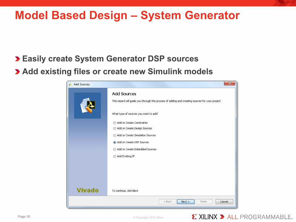
Easily create System Generator DSP sources Add existing files or create new Simulink models
Model Based Design – System Generator
Page 26

© Copyright 2012 Xilinx
Fully integrated into the Vivado IDE – Launch System Generator from the Vivado IDE
Model Based Design – System Generator
Page 27
© Copyright 2012 Xilinx
HLS: What’s different?
Established specification language – C/C++/SystemC standards
Quality of Results – Extracting parallel execution from
sequential specification
Accommodates datapath and control Complement RTL-based tools Acknowledgement of verification needs Consideration for physical interfaces
Source: IEEE Design&Test of Computers (2009) Volume: 26, Issue: 4, Publisher: IEEE Computer Society, Pages: 18-25
Page 28

© Copyright 2012 Xilinx
Starts at C – C – C++ – SystemC
Produces RTL – Verilog – VHDL – SystemC
Automates Flow – RTL Verification – IP Packaging
Vivado HLS Design Flow
Function
Architecture
IP Block
Vivado HLS
C Synthesis
RTL Design
RTL Verification
Behavioral Verification
C Wrapper
IP Package Vivado IP Integrator System Generator
Packaging
C Specification C Verification
C Design
C Test Bench
Vivado IP Packager
Page 29

© Copyright 2012 Xilinx
Core Technology
Function
Architecture
IP Block
Cod
ing
Styl
e (C
)
Parameter CTHREAD Function Loop Statement Array
Dire
ctiv
es (T
cl)
Port Clock Domain
Module Process Operation Memory
Port
able
IP
AXI4 Interface Performance Resources
INTE
RFA
CE
INLI
NE
DAT
AFLO
W
PIPE
LIN
E
ALLO
CAT
ION
PAR
TITI
ON
STR
EAM
P F F1 A L1 L2
P F F1
f
L1 L2
___ ___ ___
AXI4
UN
RO
LL
Page 30
© Copyright 2012 Xilinx
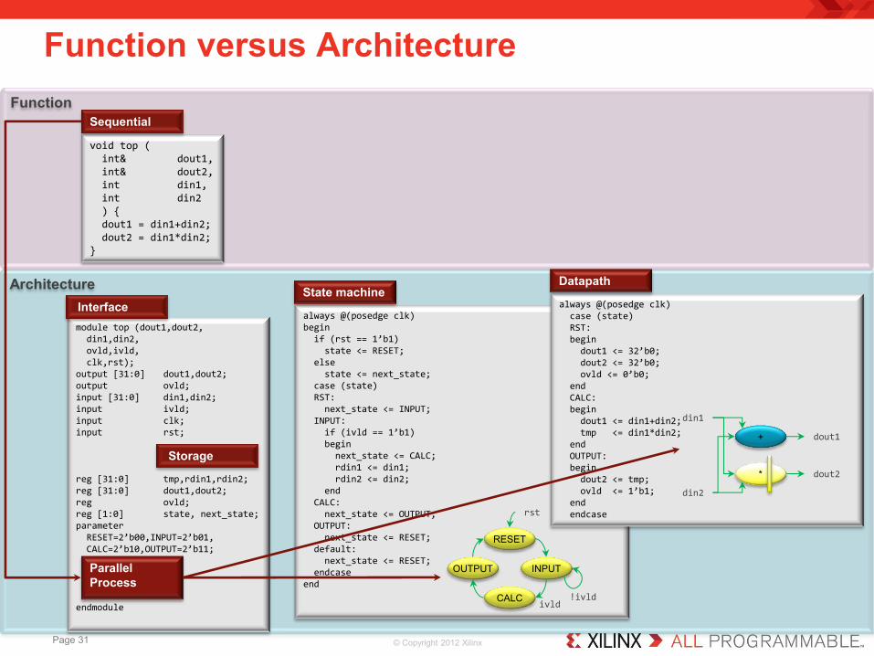
Function
Architecture
Function versus Architecture
void top ( int& dout1, int& dout2, int din1, int din2 ) { dout1 = din1+din2; dout2 = din1*din2; }
Sequential
always @(posedge clk) begin if (rst == 1’b1) state <= RESET; else state <= next_state; case (state) RST: next_state <= INPUT; INPUT: if (ivld == 1’b1) begin next_state <= CALC; rdin1 <= din1; rdin2 <= din2; end CALC: next_state <= OUTPUT; OUTPUT: next_state <= RESET; default: next_state <= RESET; endcase end
State machine
RESET
rst
INPUT OUTPUT
ivld !ivld CALC
always @(posedge clk) case (state) RST: begin dout1 <= 32’b0; dout2 <= 32’b0; ovld <= 0’b0; end CALC: begin dout1 <= din1+din2; tmp <= din1*din2; end OUTPUT: begin dout2 <= tmp; ovld <= 1’b1; end endcase
Datapath
+
*
dout1
dout2
din1
din2
module top (dout1,dout2, din1,din2, ovld,ivld, clk,rst); output [31:0] dout1,dout2; output ovld; input [31:0] din1,din2; input ivld; input clk; input rst; reg [31:0] tmp,rdin1,rdin2; reg [31:0] dout1,dout2; reg ovld; reg [1:0] state, next_state; parameter RESET=2’b00,INPUT=2’b01, CALC=2’b10,OUTPUT=2’b11; endmodule
Parallel Process
Interface
Storage
Page 31

© Copyright 2012 Xilinx
CDT based – Simplified for HLS user – Windows
• MinGW/msys included
– Linux
SystemC libraries included Video/Image functional verification: 10000x speed versus RTL simulation
Vivado HLS C Development
Page 32

© Copyright 2012 Xilinx
Design Specification – Superior language support
• C Easy, familiar • C++ Methodical • SystemC Standard
Directives – Tcl Efficient Exploration – Pragma Self-documenting
Standard Input Structured Programming
Object Oriented Programming (OOP)
System Modeling
C (C99)
CPP (Standard C++)
OSCI SystemC (IEEE 1666-2005)
Function Class Template (STL)
Module/Port Arbitrary precision Parallel process Time (Simulation Kernel) Abstraction (TLM)
Page 33

© Copyright 2012 Xilinx
Vivado HLS Synthesis
Fast for architecture exploration – Tcl-based batch mode
Scalable for ultra-large IP blocks – 200K LUT/hour
Quality of results – DSP48 inferencing – Parallelization (instruction and
task) 0
50
100
150
200
250
0 10000 20000Sy
nthe
sis
Tim
e (s
)
Design Size (LUT)
Page 34

© Copyright 2012 Xilinx
Arbitrary Precision – C
• Simulation and Synthesis – C++
• Rounding and Saturation
DSP Applications
void yuv2rgb ( pixel_t *in, pixel_t *out ) { uint8 R, G, B; int9 C, D, E, Y, U, V; const int11 Wyuv[3][3] = { {298, 0, 409}, {298, -100, -208}, {298, 516, 0}, }; Y = in->col1; U = in->col2; V = in->col3; C = Y - 16; D = U - 128; E = V - 128; R = CLIP(( Wyuv[0][0] * C + Wyuv[0][2] * E + 128) >> 8); G = CLIP(( Wyuv[1][0] * C + Wyuv[1][1] * D + Wyuv[1][2] * E + 128) >> 8); B = CLIP(( Wyuv[2][0] * C + Wyuv[2][1] * D + 128) >> 8); out->col1 = R; out->col2 = G; out->col3 = B; }
void yuv2rgb ( pixel_t *in, pixel_t *out ) { hls_ufixed<8,8,HLS_RND,HLS_SAT> R, G, B; hls_fixed<8,8,HLS_RND,HLS_SAT> Y, U, V; const ap_fixed<11,2,HLS_RND> Wyuv[3][3] = { {1, 0, 1.13983}, {1,-0.39465,-0.5806}, {1, 2.03211, 0}, }; Y = in->col1; U = in->col2; V = in->col3; R = Wyuv[0][0] * Y + Wyuv[0][2] * V; G = Wyuv[1][0] * Y + Wyuv[1][1] * U + Wyuv[1][2] * V; B = Wyuv[2][0] * Y + Wyuv[2][1] * U ; out->col1 = R; out->col2 = G; out->col3 = B; }
Page 35

© Copyright 2012 Xilinx
DSP48 inferencing
DSP Applications
#include "ap_int.h" #include <complex> using namespace std; typedef ap_int<18> data_t; typedef complex<data_t> cdata_t; cdata_t cmult ( cdata_t a, cdata_t b ) { return a*b; }
• Expression matching: pre/mult/post • Coding Style • Attributes
areal
aimag
breal
bimag
+
* - * * *
rreal
rimag
Page 36
© Copyright 2012 Xilinx
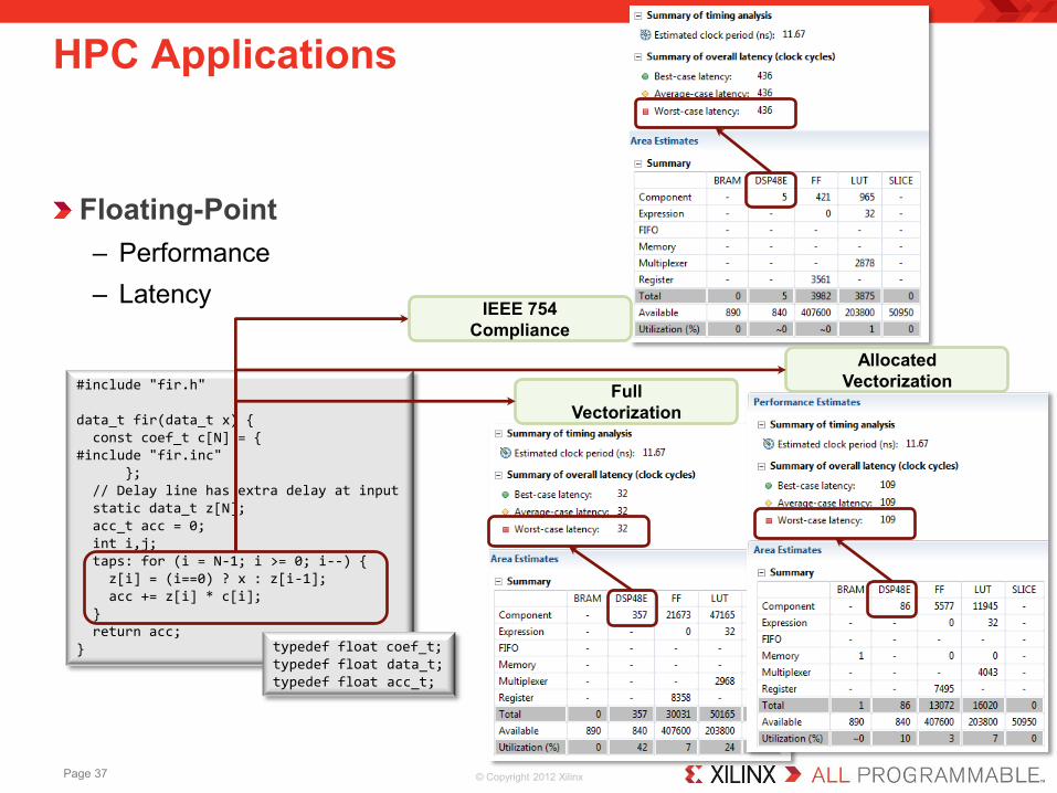
Floating-Point – Performance – Latency
HPC Applications
#include "fir.h" data_t fir(data_t x) { const coef_t c[N] = { #include "fir.inc" }; // Delay line has extra delay at input static data_t z[N]; acc_t acc = 0; int i,j; taps: for (i = N-1; i >= 0; i--) { z[i] = (i==0) ? x : z[i-1]; acc += z[i] * c[i]; } return acc; } typedef float coef_t;
typedef float data_t; typedef float acc_t;
IEEE 754 Compliance
Full Vectorization
Allocated Vectorization
Page 37

© Copyright 2012 Xilinx
Bridging the Gap – Algorithm designer to Hardware designer
Creating with C – Concise Specification – Algorithm Exploration – Fast Verification
Reusing with HLS – Architecture Exploration – Cost/Power Reduction – Portable IP
Vivado High-Level Synthesis – Demo
Start Demo >
Vivado HLS
High-Level Synthesis
RTL Design
Verification
Architectural Verification
C Wrapper
C Design
C Test Bench
IP Packager IP Integrator System Generator RTL
Packaging
Specification & Debug
Page 38

© Copyright 2012 Xilinx
Vivado Design Suite Elements
Integrated Design Environment D
ebug and Analysis
Shared Scalable Data M
odel
Accelerating Implementation
Hierarchical Chip Planning
Deterministic P&R, Closure Automation
ECO
P o w e r
Fast Synthesis w/ SDC Constraints
Scalable to 100M Gates
Page 39

© Copyright 2012 Xilinx
Hierarchical Chip Planning
Deterministic P&R, Closure Automation
ECO
P o w e r
Fast Synthesis w/ SDC Constraints
Full compile
Full compile
Full compile
Incremental
Full compile
Incremental
Deterministic Design Closure
T (hrs)
Optimizer
Analyzer
TOP
MEM DMA
CPU CNTRL DATA
Page 40
© Copyright 2012 Xilinx
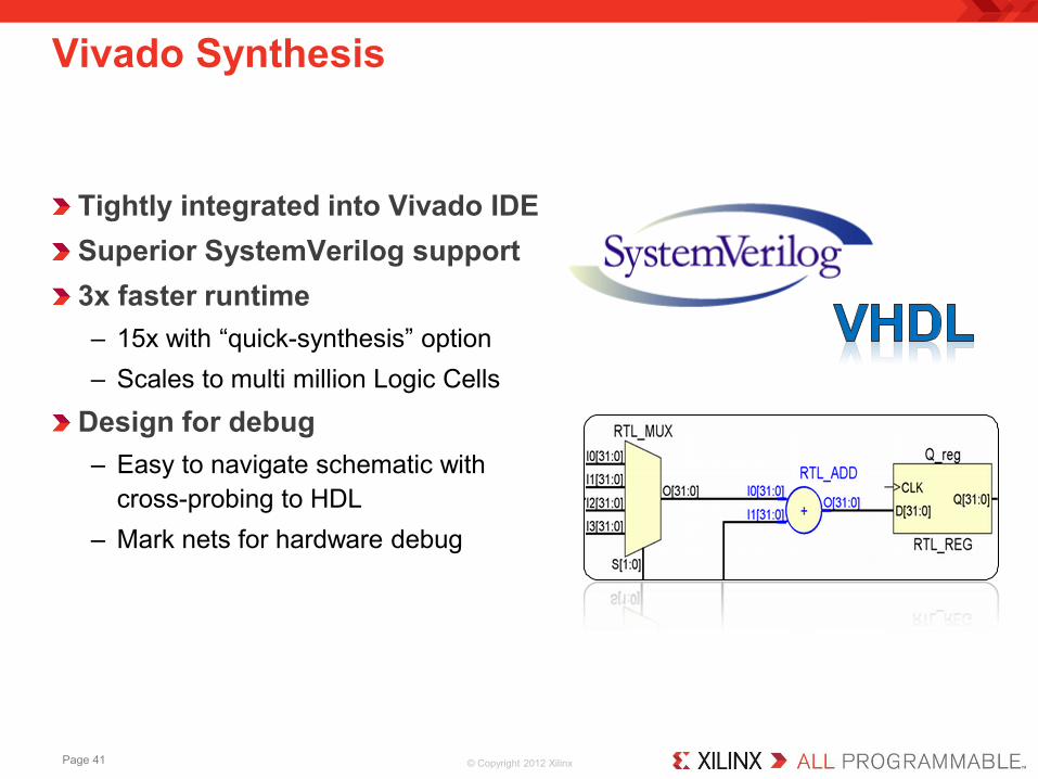
Tightly integrated into Vivado IDE Superior SystemVerilog support 3x faster runtime – 15x with “quick-synthesis” option – Scales to multi million Logic Cells
Design for debug – Easy to navigate schematic with
cross-probing to HDL – Mark nets for hardware debug
Vivado Synthesis
Page 41

© Copyright 2012 Xilinx
Example: Counting 1’s in a vector
Higher-level RTL Synthesis Control Data Flow Graph Optimization
c
a[3]
a[4] a[5]
a[6]
a[0]
a[1] a[2] +
+
+
a[7]
c = 0; for (i=0; i<8; i=i+1) if (a[i] == 1) c = c + 1;
c = a[0] + a[1] + a[2] + a[3] + a[4] + a[5] + a[6] + a[7];
0
+ c
a[7] a[6] a[0]
+1 …
+1 +1
Traditional Synthesis tools – Area: 8 ADD + 8 MUX – Depth: O(n)
Optimized by Vivado Synthesis – Area: 4 smaller ADD 4x smaller – Depth: O(log(n))
Original code Optimized & unrolled
Page 42

© Copyright 2012 Xilinx
Vivado Key Enabling Technologies Analytical Place & Route Engine
Traditional P&R Vivado P&R
“Cost” Criteria 1 dimension: timing minimization 3 dimensions: timing, congestion,
wire length minimization
Primary Algorithm
“Simulated Annealing”: Random, iterative search based on initial seed
Analytical: solves simultaneous equations to minimize all dimensions
Runtime Unpredictable Due to random nature of algorithm. Exponential with congestion
Very predictable Manages congestion
Scalability Poor results as design approaches 1M logic cells
Will handle 10M+ logic cells with predictable results
Tim
ing
Cos
t f(x
)
Placement Solution x (found by random moves and seeds)
initial random seed
best solution found
optimal solution (not found)
not routable
random moves
Page 43
© Copyright 2012 Xilinx
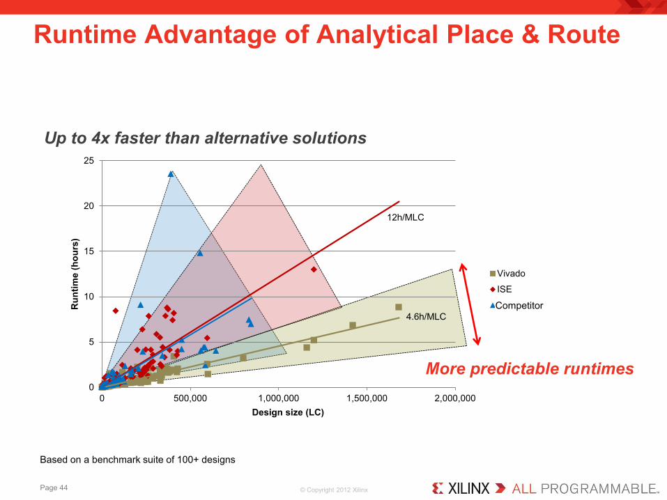
Runtime Advantage of Analytical Place & Route
Up to 4x faster than alternative solutions
4.6h/MLC
12h/MLC
0
5
10
15
20
25
0 500,000 1,000,000 1,500,000 2,000,000
Run
time
(hou
rs)
Design size (LC)
Vivado
ISE
Compet
More predictable runtimes
Based on a benchmark suite of 100+ designs
Competitor
Page 44

© Copyright 2012 Xilinx
Customer proven: All SSI customers using Vivado today!
Vivado Design Example 1.2 M LC Virtex-7 2000T Design*
*Zynq Emulation Platform
ISE Vivado
P&R runtime 13 hrs 5 hrs
Memory usage 16 GB 9 GB
Wire length and congestion
Significantly reduced
Page 45
© Copyright 2012 Xilinx
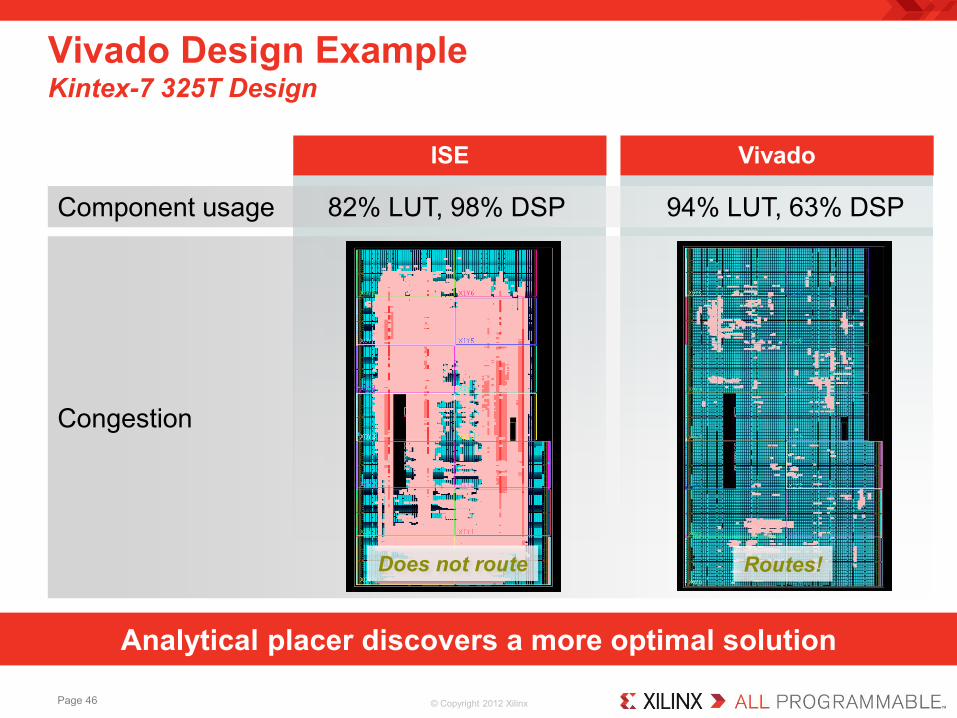
Analytical placer discovers a more optimal solution
Vivado Design Example Kintex-7 325T Design
ISE Vivado
Component usage 82% LUT, 98% DSP 94% LUT, 63% DSP
Congestion
Does not route Routes!
Page 46
© Copyright 2012 Xilinx
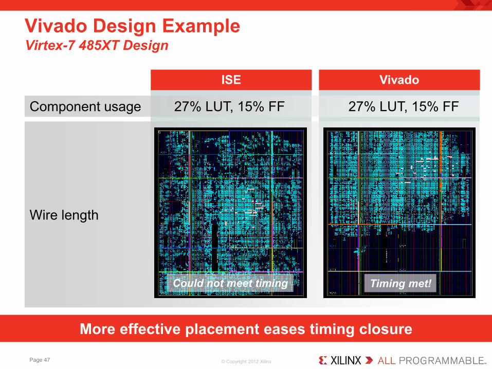
More effective placement eases timing closure
Vivado Design Example Virtex-7 485XT Design
ISE Vivado
Component usage 27% LUT, 15% FF 27% LUT, 15% FF
Wire length
Could not meet timing Timing met!
Page 47

© Copyright 2012 Xilinx
Design & Analysis Environment – IP Integrator & IP Catalog – Implementation, incremental editing – Floorplanner and Design Editor
Vivado IDE
– Estimations at any stage of design flow – Cross-probing / Tcl interaction – Report and log browser
Page 48
© Copyright 2012 Xilinx
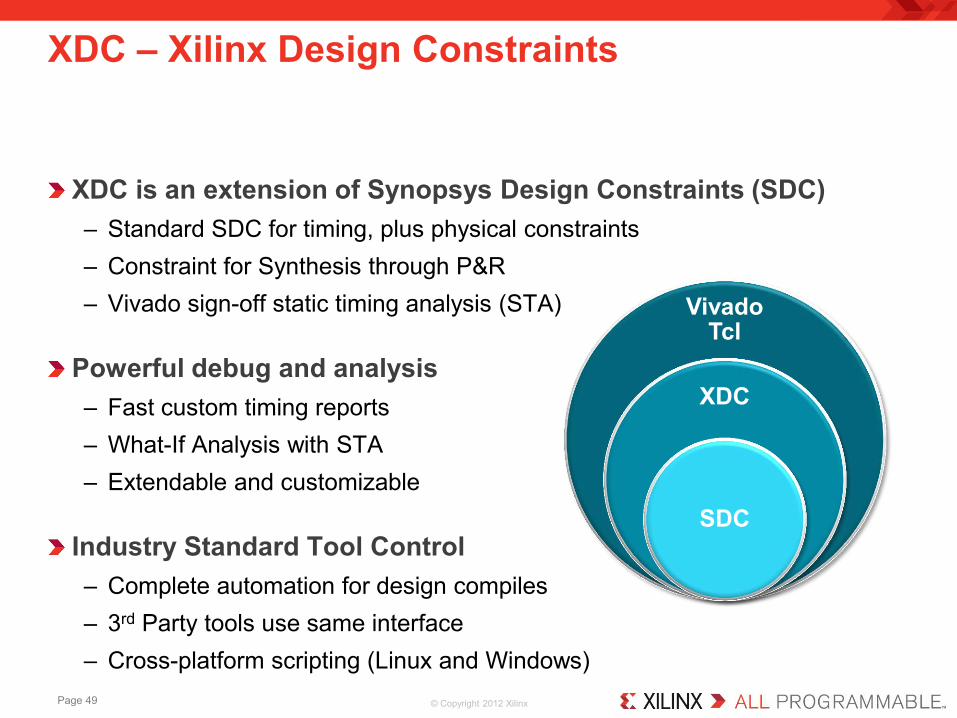
XDC is an extension of Synopsys Design Constraints (SDC) – Standard SDC for timing, plus physical constraints – Constraint for Synthesis through P&R – Vivado sign-off static timing analysis (STA)
Powerful debug and analysis – Fast custom timing reports – What-If Analysis with STA – Extendable and customizable
Industry Standard Tool Control – Complete automation for design compiles – 3rd Party tools use same interface – Cross-platform scripting (Linux and Windows)
XDC – Xilinx Design Constraints
Vivado Tcl
XDC
SDC
Page 49
© Copyright 2012 Xilinx
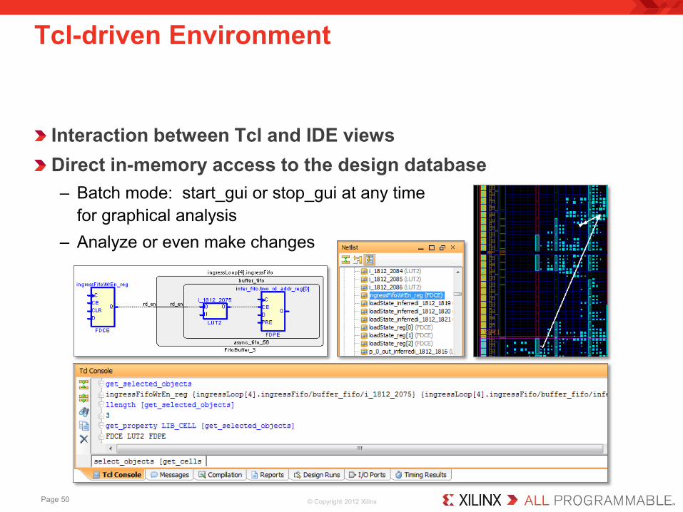
Interaction between Tcl and IDE views Direct in-memory access to the design database – Batch mode: start_gui or stop_gui at any time
for graphical analysis – Analyze or even make changes
Tcl-driven Environment
Page 50

© Copyright 2012 Xilinx
Rodin supports two flows: – Project – Batch (Project-less)
Project Flow – Project infrastructure – IDE or Tcl script – Reports automatically
generated
Batch Flow – No project infrastructure – Tcl based – Use GUI for visualization
via start_gui – Must manually create
reports and checkpoints
Project vs. Batch Flows
Batch Based Project Based
IDE Script Script
read_verilog …
read_vhdl …
read_edif …
…
synth_design …
report_timing_summary
write_checkpoint …
opt_design
place_design
report_timing_summary
write_checkpoint …
route_design
report_timing_summary
write_checkpoint …
create_project …
add_files …
import_files …
…
launch_run synth_1
wait_on_run …
open_run …
report_timing_summary
launch_runs impl_1
wait_on_run …
open_run …
Page 51

© Copyright 2012 Xilinx
Create Schematic from selected Timing Path(s) View logic levels across critical timing paths Expand connectivity and select parent hierarchies
Analysis at Schematic View
Page 52

© Copyright 2012 Xilinx
Select Paths in Timing Results, view objects cross-selected in other windows
Analysis at Placed Design View
Page 53
© Copyright 2012 Xilinx
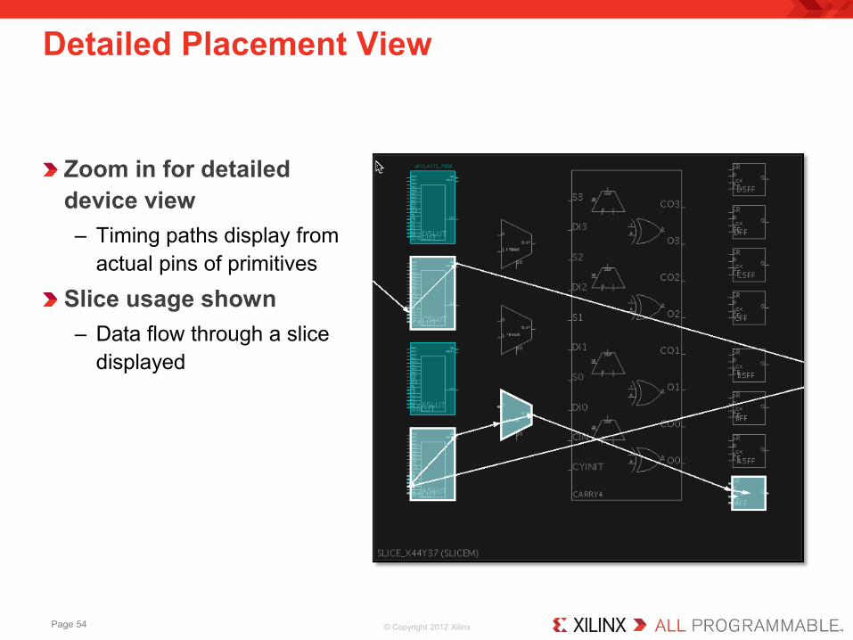
Zoom in for detailed device view – Timing paths display from
actual pins of primitives
Slice usage shown – Data flow through a slice
displayed
Detailed Placement View
Page 54

© Copyright 2012 Xilinx
View Routing Resources View route used Cross-probing enabled Change layers & colors
Analysis at Routed Design View
Page 55
© Copyright 2012 Xilinx
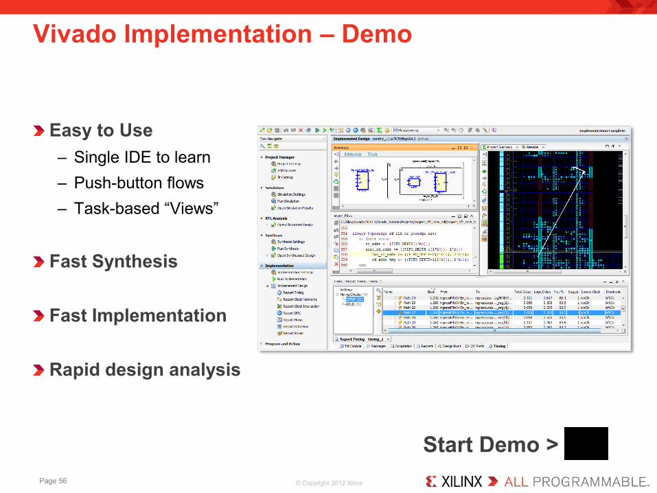
Easy to Use – Single IDE to learn – Push-button flows – Task-based “Views”
Fast Synthesis
Fast Implementation
Rapid design analysis
Vivado Implementation – Demo
Start Demo > Page 56

© Copyright 2012 Xilinx
Incremental Implementation – Ideal for small changes (<5%) – Timing preservation from run to run
• Timing changes limited to modified areas – Runtime: 2.5x faster
Post P&R with Device Editor – All FPGA elements are visible with exact
placement and precise routing topology – Rapid post-route design editing
• Make design changes and auto-route nets • Modify routing, placement, logic
– GUI or Tcl based
Make Last Minute Design Changes without Re-building the Entire Design
Full compile
Full compile
Full compile
Incremental
Full compile
T (hrs)
Incremental
Page 57
© Copyright 2012 Xilinx
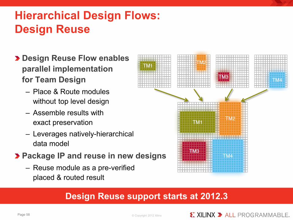
Design Reuse Flow enables parallel implementation for Team Design – Place & Route modules
without top level design – Assemble results with
exact preservation – Leverages natively-hierarchical
data model
Package IP and reuse in new designs – Reuse module as a pre-verified
placed & routed result
Hierarchical Design Flows: Design Reuse
Design Reuse support starts at 2012.3
Page 58

© Copyright 2012 Xilinx
System Flexibility – Swap functions and perform remote
updates while system is operational
Cost and Size Reduction – Time-multiplexing hardware requires
a smaller FPGA – Reduces board space – Minimizes bitstream storage
Power Reduction – Via smaller or/and fewer devices – Swap out power-hungry tasks
Hierarchical Design Flows: Partial Reconfiguration
Partial Reconfiguration support starts in 2013
Page 59
© Copyright 2012 Xilinx
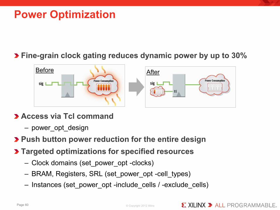
Fine-grain clock gating reduces dynamic power by up to 30% Access via Tcl command – power_opt_design
Push button power reduction for the entire design Targeted optimizations for specified resources – Clock domains (set_power_opt -clocks) – BRAM, Registers, SRL (set_power_opt -cell_types) – Instances (set_power_opt -include_cells / -exclude_cells)
Power Optimization
After Before
Page 60

© Copyright 2012 Xilinx
Accurate power and thermal analysis Power estimates at every stage after synthesis Analyze power by consumption type
– Each view deconstructed with low-level details What-if analysis by varying switching activity Extensive debug capabilities via cross-probing Export data to Xilinx Power Estimator
Power Analysis
Page 61