Viterbi IP Core User Guide - intel.com · • Errata for Viterbi IP core in the Knowledge Base 1.6...
38
Transcript of Viterbi IP Core User Guide - intel.com · • Errata for Viterbi IP core in the Knowledge Base 1.6...

Viterbi IP Core User Guide
Updated for Intel® Quartus® Prime Design Suite: 17.1
SubscribeSend Feedback
UG-VITERBI | 2017.11.06Latest document on the web: PDF | HTML

Contents
1 About the Viterbi IP Core................................................................................................. 31.1 Intel® DSP IP Core Features.....................................................................................31.2 Viterbi IP Core Features...........................................................................................41.3 DSP IP Core Device Family Support...........................................................................41.4 DSP IP Core Verification...........................................................................................51.5 Viterbi IP Core Release Information...........................................................................51.6 Viterbi IP Core Performance and Resource Utilization...................................................5
2 Viterbi IP Core Getting Started........................................................................................ 92.1 Installing and Licensing Intel FPGA IP Cores............................................................... 9
2.1.1 Intel FPGA IP Evaluation Mode......................................................................92.1.2 Viterbi IP Core Intel FPGA IP Evaluation Mode Timeout Behavior......................12
2.2 IP Catalog and Parameter Editor............................................................................. 122.3 Generating IP Cores (Intel Quartus Prime Pro Edition)................................................14
2.3.1 IP Core Generation Output (Intel Quartus Prime Pro Edition)...........................152.4 Simulating Intel FPGA IP Cores............................................................................... 182.5 DSP Builder for Intel FPGAs Design Flow.................................................................. 18
3 Viterbi IP Core Functional Description........................................................................... 193.1 Decoder...............................................................................................................193.2 Convolutional Encoder........................................................................................... 193.3 Trellis Coded Modulation........................................................................................ 19
3.3.1 Half-Rate Convolutional Codes.................................................................... 203.3.2 Trellis Decoder..........................................................................................223.3.3 About Converting Received Signals..............................................................233.3.4 Trellis Termination.....................................................................................253.3.5 Trellis Initialization ................................................................................... 25
3.4 Viterbi IP Core Parameters..................................................................................... 253.4.1 Architecture............................................................................................. 253.4.2 Code Sets................................................................................................ 283.4.3 Viterbi Parameters.................................................................................... 283.4.4 Test Data.................................................................................................30
3.5 Viterbi IP Core Interfaces and Signals......................................................................313.5.1 Avalon-ST Interfaces in DSP IP Cores.......................................................... 313.5.2 Global Signals.......................................................................................... 323.5.3 Avalon-ST Sink Signals.............................................................................. 323.5.4 Avalon Source-ST Signals...........................................................................333.5.5 Configuration Signals.................................................................................343.5.6 Status Signals.......................................................................................... 343.5.7 Viterbi IP Core Timing Diagrams................................................................. 35
A Viterbi IP Core User Guide Document Archives.............................................................. 37
5 Document Revision History............................................................................................ 38
Contents
Viterbi IP Core User Guide2
1 About the Viterbi IP Core
Related Links
• Introduction to Intel FPGA IP CoresProvides general information about all Intel FPGA IP cores, includingparameterizing, generating, upgrading, and simulating IP cores.
• Creating Version-Independent IP and Qsys Simulation ScriptsCreate simulation scripts that do not require manual updates for software or IPversion upgrades.
• Project Management Best PracticesGuidelines for efficient management and portability of your project and IP files.
• Viterbi IP Core User Guide Document Archives on page 37Provides a list of user guides for previous versions of the Viterbi IP core.
1.1 Intel® DSP IP Core Features
• Avalon® Streaming (Avalon-ST) interfaces
• DSP Builder for Intel® FPGAs ready
• Testbenches to verify the IP core
• IP functional simulation models for use in Intel-supported VHDL and Verilog HDLsimulators
UG-VITERBI | 2017.11.06
Intel Corporation. All rights reserved. Intel, the Intel logo, Altera, Arria, Cyclone, Enpirion, MAX, Nios, Quartusand Stratix words and logos are trademarks of Intel Corporation or its subsidiaries in the U.S. and/or othercountries. Intel warrants performance of its FPGA and semiconductor products to current specifications inaccordance with Intel's standard warranty, but reserves the right to make changes to any products and servicesat any time without notice. Intel assumes no responsibility or liability arising out of the application or use of anyinformation, product, or service described herein except as expressly agreed to in writing by Intel. Intelcustomers are advised to obtain the latest version of device specifications before relying on any publishedinformation and before placing orders for products or services.*Other names and brands may be claimed as the property of others.
ISO9001:2008Registered

1.2 Viterbi IP Core Features
• High-speed parallel architecture:
— Performance of over 250 megabits per second (Mbps)
— Fully parallel operation
— Optimized block decoding and continuous decoding
• Low to medium-speed, hybrid architecture:
— Configurable number of add compare and select (ACS) units
— Memory-based architecture
— Wide range of performance; wide range of logic area
• Fully parameterized Viterbi decoder, including:
— Number of coded bits
— Constraint length
— Number of soft bits
— Traceback length
— Polynomial for each coded bit
• Variable constraint length
• Trellis coded modulation (TCM) option
1.3 DSP IP Core Device Family Support
Intel offers the following device support levels for Intel FPGA IP cores:
• Advance support—the IP core is available for simulation and compilation for thisdevice family. FPGA programming file (.pof) support is not available for QuartusPrime Pro Stratix 10 Edition Beta software and as such IP timing closure cannot beguaranteed. Timing models include initial engineering estimates of delays basedon early post-layout information. The timing models are subject to change assilicon testing improves the correlation between the actual silicon and the timingmodels. You can use this IP core for system architecture and resource utilizationstudies, simulation, pinout, system latency assessments, basic timing assessments(pipeline budgeting), and I/O transfer strategy (data-path width, burst depth, I/Ostandards tradeoffs).
• Preliminary support—Intel verifies the IP core with preliminary timing models forthis device family. The IP core meets all functional requirements, but might still beundergoing timing analysis for the device family. You can use it in productiondesigns with caution.
• Final support—Intel verifies the IP core with final timing models for this devicefamily. The IP core meets all functional and timing requirements for the devicefamily. You can use it in production designs.
Table 1. DSP IP Core Device Family Support
Device Family Support
Arria® II GX Final
Arria II GZ Final
continued...
1 About the Viterbi IP Core
UG-VITERBI | 2017.11.06
Viterbi IP Core User Guide4

Device Family Support
Arria V Final
Intel Arria 10 Final
Cyclone® IV Final
Cyclone V Final
Intel Cyclone 10 Final
Intel MAX® 10 FPGA Final
Stratix® IV GT Final
Stratix IV GX/E Final
Stratix V Final
Intel Stratix 10 Advance
Other device families No support
1.4 DSP IP Core Verification
Before releasing a version of an IP core, Intel runs comprehensive regression tests toverify its quality and correctness. Intel generates custom variations of the IP core toexercise the various parameter options and thoroughly simulates the resultingsimulation models with the results verified against master simulation models.
1.5 Viterbi IP Core Release Information
Use the release information when licensing the IP core.
Table 2. Release Information
Item Description
Version 17.1
Release Date November 2017
Ordering Code IP-VITERBI/HS (parallel architecture) IP-VITERBI/SS (hybridarchitecture)
Intel verifies that the current version of the Quartus Prime software compiles theprevious version of each IP core. Intel does not verify that the Quartus Prime softwarecompiles IP core versions older than the previous version. The Intel FPGA IP ReleaseNotes lists any exceptions.
Related Links
• Intel FPGA IP Release Notes
• Errata for Viterbi IP core in the Knowledge Base
1.6 Viterbi IP Core Performance and Resource Utilization
This typical expected performance uses different architectures and constraint length,L, combinations, and ACS units, A, and the Quartus Prime software. Performancelargely depends on constraint length, L.
1 About the Viterbi IP Core
UG-VITERBI | 2017.11.06
Viterbi IP Core User Guide5

Hybrid Architecture
The typical expected performance for a hybrid Viterbi IP core uses the Quartus Primesoftware with the Arria V (5AGXFB3H4F40C4), Cyclone V (5CGXFC7D6F31C6), andStratix V (5SGSMD4H2F35C2) devices and the following parameters:
• v = 6 × L
• softbits = 3
• N = 2
where:
• v is the traceback length
• L is the constraint length
• N is the number of coded bits
• A is the number of ACS units
Table 3. Typical Performance
Parameters Device ALM fMAX (MHz) Memory Registers
L A M10K M20K Primary Secondary
5 1 Arria 10 401 383 -- 3 422 40
5 1 Arria V 323 201 5 -- 390 60
5 1 Cyclone V 324 172 5 -- 390 53
5 1 Stratix V 316 432 -- 5 388 44
7 1 Arria 10 521 370 -- 4 559 50
7 1 Arria V 427 207 6 -- 507 58
7 1 Cyclone V 427 185 6 -- 507 74
7 1 Stratix V 417 438 -- 6 506 51
7 2 Arria 10 622 363 -- 4 670 51
7 2 Arria V 529 215 6 -- 625 71
7 2 Cyclone V 532 180 6 -- 625 74
7 2 Stratix V 502 408 -- 6 625 56
7 4 Arria 10 835 366 -- 4 885 101
7 4 Arria V 744 204 6 -- 856 99
7 4 Cyclone V 746 173 6 -- 856 100
7 4 Stratix V 652 382 -- 6 856 82
9 1 Arria 10 932 343 -- 9 970 88
1 Arria V 792 190 11 -- 927 90
9 1 Cyclone V 794 176 11 -- 926 96
9 1 Stratix V 777 393 -- 11 924 94
9 16 Arria V 2,118 188 17 -- 2,743 309
continued...
1 About the Viterbi IP Core
UG-VITERBI | 2017.11.06
Viterbi IP Core User Guide6

Parameters Device ALM fMAX (MHz) Memory Registers
L A M10K M20K Primary Secondary
9 16 Cyclone V 2,119 163 17 -- 2,744 275
9 16 Stratix V 1,887 348 -- 17 2,738 198
9 2 Arria 10 1,029 363 -- 9 1,091 74
9 2 Arria V 889 205 11 -- 1,053 98
9 2 Cyclone V 889 180 11 -- 1,053 96
9 2 Stratix V 883 377 -- 11 1,053 115
9 4 Arria 10 1,240 298 -- 9 1,321 87
9 4 Arria V 1,097 201 11 -- 1,302 137
9 4 Cyclone V 1,096 159 11 -- 1,302 126
9 4 Stratix V 1,021 390 -- 11 1,302 119
9 8 Arria V 1,465 197 13 -- 1,788 193
9 8 Cyclone V 1,465 163 13 -- 1,789 191
9 8 Stratix V 1,398 351 -- 13 1,790 154
Parallel Architecture
The typical expected performance for a parallel Viterbi IP core uses the Quartus Primesoftware with the Arria V (5AGXFB3H4F40C4), Cyclone V (5CGXFC7D6F31C6), andStratix V (5SGSMD4H2F35C2) devices. The following parameters apply:
• v = 6 ×L
• N = 2
where:
• v is the traceback length
• L is the constraint length
• N is the number of coded bits
Table 4. Typical Performance
Parameters Device ALMs fMAX(MHz)
Memory Registers
softbits L Optimization Best State Finder M10K M20K Primary Secondary
5 3 — On Arria 10 420 400 -- 5 500 63
7 3 — On Arria 10 453 351 -- 5 534 75
3 3 — Off Arria 10 396 423 -- 5 473 39
5 3 — Off Arria 10 420 400 -- 5 500 63
7 3 — Off Arria 10 453 351 -- 5 534 75
3 7 Block Off Arria 10 1,454 354 -- 3 817 154
3 7 Block Off Arria V 1,537 201 5 -- 1,166 168
3 7 Block Off Cyclone V 1,544 149 5 -- 1,167 88
continued...
1 About the Viterbi IP Core
UG-VITERBI | 2017.11.06
Viterbi IP Core User Guide7
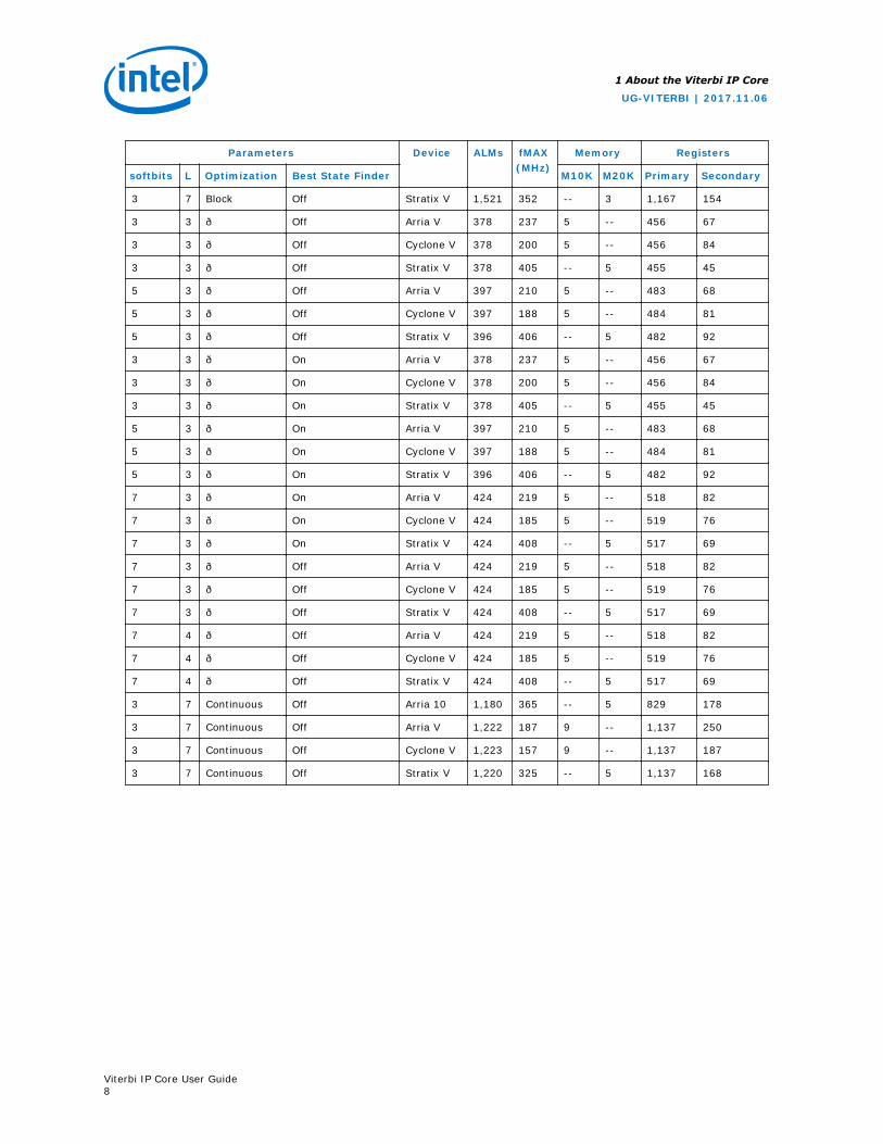
Parameters Device ALMs fMAX(MHz)
Memory Registers
softbits L Optimization Best State Finder M10K M20K Primary Secondary
3 7 Block Off Stratix V 1,521 352 -- 3 1,167 154
3 3 — Off Arria V 378 237 5 -- 456 67
3 3 — Off Cyclone V 378 200 5 -- 456 84
3 3 — Off Stratix V 378 405 -- 5 455 45
5 3 — Off Arria V 397 210 5 -- 483 68
5 3 — Off Cyclone V 397 188 5 -- 484 81
5 3 — Off Stratix V 396 406 -- 5 482 92
3 3 — On Arria V 378 237 5 -- 456 67
3 3 — On Cyclone V 378 200 5 -- 456 84
3 3 — On Stratix V 378 405 -- 5 455 45
5 3 — On Arria V 397 210 5 -- 483 68
5 3 — On Cyclone V 397 188 5 -- 484 81
5 3 — On Stratix V 396 406 -- 5 482 92
7 3 — On Arria V 424 219 5 -- 518 82
7 3 — On Cyclone V 424 185 5 -- 519 76
7 3 — On Stratix V 424 408 -- 5 517 69
7 3 — Off Arria V 424 219 5 -- 518 82
7 3 — Off Cyclone V 424 185 5 -- 519 76
7 3 — Off Stratix V 424 408 -- 5 517 69
7 4 — Off Arria V 424 219 5 -- 518 82
7 4 — Off Cyclone V 424 185 5 -- 519 76
7 4 — Off Stratix V 424 408 -- 5 517 69
3 7 Continuous Off Arria 10 1,180 365 -- 5 829 178
3 7 Continuous Off Arria V 1,222 187 9 -- 1,137 250
3 7 Continuous Off Cyclone V 1,223 157 9 -- 1,137 187
3 7 Continuous Off Stratix V 1,220 325 -- 5 1,137 168
1 About the Viterbi IP Core
UG-VITERBI | 2017.11.06
Viterbi IP Core User Guide8

2 Viterbi IP Core Getting Started
1.
2.1 Installing and Licensing Intel FPGA IP Cores
The Intel Quartus Prime software installation includes the Intel FPGA IP library. Thislibrary provides many useful IP cores for your production use without the need for anadditional license. Some Intel FPGA IP cores require purchase of a separate license forproduction use. The Intel FPGA IP Evaluation Mode allows you to evaluate theselicensed Intel FPGA IP cores in simulation and hardware, before deciding to purchase afull production IP core license. You only need to purchase a full production license forlicensed Intel IP cores after you complete hardware testing and are ready to use theIP in production.
The Intel Quartus Prime software installs IP cores in the following locations by default:
Figure 1. IP Core Installation Path
intelFPGA(_pro)
quartus - Contains the Intel Quartus Prime softwareip - Contains the Intel FPGA IP library and third-party IP cores
altera - Contains the Intel FPGA IP library source code<IP name> - Contains the Intel FPGA IP source files
Table 5. IP Core Installation Locations
Location Software Platform
<drive>:\intelFPGA_pro\quartus\ip\altera Intel Quartus Prime Pro Edition Windows*
<drive>:\intelFPGA\quartus\ip\altera Intel Quartus Prime StandardEdition
Windows
<home directory>:/intelFPGA_pro/quartus/ip/altera Intel Quartus Prime Pro Edition Linux*
<home directory>:/intelFPGA/quartus/ip/altera Intel Quartus Prime StandardEdition
Linux
2.1.1 Intel FPGA IP Evaluation Mode
The free Intel FPGA IP Evaluation Mode allows you to evaluate licensed Intel FPGA IPcores in simulation and hardware before purchase. Intel FPGA IP Evaluation Modesupports the following evaluations without additional license:
UG-VITERBI | 2017.11.06
Intel Corporation. All rights reserved. Intel, the Intel logo, Altera, Arria, Cyclone, Enpirion, MAX, Nios, Quartusand Stratix words and logos are trademarks of Intel Corporation or its subsidiaries in the U.S. and/or othercountries. Intel warrants performance of its FPGA and semiconductor products to current specifications inaccordance with Intel's standard warranty, but reserves the right to make changes to any products and servicesat any time without notice. Intel assumes no responsibility or liability arising out of the application or use of anyinformation, product, or service described herein except as expressly agreed to in writing by Intel. Intelcustomers are advised to obtain the latest version of device specifications before relying on any publishedinformation and before placing orders for products or services.*Other names and brands may be claimed as the property of others.
ISO9001:2008Registered

• Simulate the behavior of a licensed Intel FPGA IP core in your system.
• Verify the functionality, size, and speed of the IP core quickly and easily.
• Generate time-limited device programming files for designs that include IP cores.
• Program a device with your IP core and verify your design in hardware.
Intel FPGA IP Evaluation Mode supports the following operation modes:
• Tethered—Allows running the design containing the licensed Intel FPGA IPindefinitely with a connection between your board and the host computer.Tethered mode requires a serial joint test action group (JTAG) cable connectedbetween the JTAG port on your board and the host computer, which is running theIntel Quartus Prime Programmer for the duration of the hardware evaluationperiod. The Programmer only requires a minimum installation of the Intel QuartusPrime software, and requires no Intel Quartus Prime license. The host computercontrols the evaluation time by sending a periodic signal to the device via theJTAG port. If all licensed IP cores in the design support tethered mode, theevaluation time runs until any IP core evaluation expires. If all of the IP coressupport unlimited evaluation time, the device does not time-out.
• Untethered—Allows running the design containing the licensed IP for a limitedtime. The IP core reverts to untethered mode if the device disconnects from thehost computer running the Intel Quartus Prime software. The IP core also revertsto untethered mode if any other licensed IP core in the design does not supporttethered mode.
When the evaluation time expires for any licensed Intel FPGA IP in the design, thedesign stops functioning. All IP cores that use the Intel FPGA IP Evaluation Mode timeout simultaneously when any IP core in the design times out. When the evaluationtime expires, you must reprogram the FPGA device before continuing hardwareverification. To extend use of the IP core for production, purchase a full productionlicense for the IP core.
You must purchase the license and generate a full production license key before youcan generate an unrestricted device programming file. During Intel FPGA IP EvaluationMode, the Compiler only generates a time-limited device programming file (<projectname>_time_limited.sof) that expires at the time limit.
2 Viterbi IP Core Getting Started
UG-VITERBI | 2017.11.06
Viterbi IP Core User Guide10

Figure 2. Intel FPGA IP Evaluation Mode Flow
Install the Intel Quartus Prime Software with Intel FPGA IP Library
Parameterize and Instantiate aLicensed Intel FPGA IP Core
Purchase a Full Production IP License
Verify the IP in a Supported Simulator
Compile the Design in theIntel Quartus Prime Software
Generate a Time-Limited DeviceProgramming File
Program the Intel FPGA Deviceand Verify Operation on the Board
No
Yes
IP Ready forProduction Use?
Include Licensed IP in Commercial Products
Note: Refer to each IP core's user guide for parameterization steps and implementationdetails.
Intel licenses IP cores on a per-seat, perpetual basis. The license fee includes first-year maintenance and support. You must renew the maintenance contract to receiveupdates, bug fixes, and technical support beyond the first year. You must purchase afull production license for Intel FPGA IP cores that require a production license, beforegenerating programming files that you may use for an unlimited time. During IntelFPGA IP Evaluation Mode, the Compiler only generates a time-limited deviceprogramming file (<project name>_time_limited.sof) that expires at the timelimit. To obtain your production license keys, visit the Self-Service Licensing Center orcontact your local Intel FPGA representative.
The Intel FPGA Software License Agreements govern the installation and use oflicensed IP cores, the Intel Quartus Prime design software, and all unlicensed IP cores.
2 Viterbi IP Core Getting Started
UG-VITERBI | 2017.11.06
Viterbi IP Core User Guide11

Related Links
• Intel Quartus Prime Licensing Site
• Intel FPGA Software Installation and Licensing
2.1.2 Viterbi IP Core Intel FPGA IP Evaluation Mode Timeout Behavior
All IP cores in a device time out simultaneously when the most restrictive evaluationtime is reached. If there is more than one IP core in a design, the time-out behavior ofthe other IP cores may mask the time-out behavior of a specific IP core .
For IP cores, the untethered time-out is 1 hour; the tethered time-out value isindefinite. Your design stops working after the hardware evaluation time expires. TheQuartus Prime software uses Intel FPGA IP Evaluation Mode Files (.ocp) in yourproject directory to identify your use of the Intel FPGA IP Evaluation Mode evaluationprogram. After you activate the feature, do not delete these files..
When the evaluation time expires the decbit signal goes low .
Related Links
AN 320: OpenCore Plus Evaluation of Megafunctions
2.2 IP Catalog and Parameter Editor
The IP Catalog displays the IP cores available for your project. Use the followingfeatures of the IP Catalog to locate and customize an IP core:
• Filter IP Catalog to Show IP for active device family or Show IP for alldevice families. If you have no project open, select the Device Family in IPCatalog.
• Type in the Search field to locate any full or partial IP core name in IP Catalog.
• Right-click an IP core name in IP Catalog to display details about supporteddevices, to open the IP core's installation folder, and for links to IP documentation.
• Click Search for Partner IP to access partner IP information on the web.
The parameter editor prompts you to specify an IP variation name, optional ports, andoutput file generation options. The parameter editor generates a top-level IntelQuartus Prime IP file (.ip) for an IP variation in Intel Quartus Prime Pro Editionprojects.
The parameter editor generates a top-level Quartus IP file (.qip) for an IP variationin Intel Quartus Prime Standard Edition projects. These files represent the IP variationin the project, and store parameterization information.
2 Viterbi IP Core Getting Started
UG-VITERBI | 2017.11.06
Viterbi IP Core User Guide12

Figure 3. IP Parameter Editor (Intel Quartus Prime Pro Edition)
IP Parameters IP Block Symbol
Figure 4. IP Parameter Editor (Intel Quartus Prime Standard Edition)
IP Port and ParameterDetails
Specify IP Variation Nameand Target Device
2 Viterbi IP Core Getting Started
UG-VITERBI | 2017.11.06
Viterbi IP Core User Guide13

2.3 Generating IP Cores (Intel Quartus Prime Pro Edition)
Quickly configure Intel FPGA IP cores in the Intel Quartus Prime parameter editor.Double-click any component in the IP Catalog to launch the parameter editor. Theparameter editor allows you to define a custom variation of the IP core. The parametereditor generates the IP variation synthesis and optional simulation files, and addsthe .ip file representing the variation to your project automatically.
Figure 5. IP Parameter Editor (Intel Quartus Prime Pro Edition)
IP Parameters IP Block Symbol
Follow these steps to locate, instantiate, and customize an IP core in the parametereditor:
1. Create or open an Intel Quartus Prime project (.qpf) to contain the instantiatedIP variation.
2. In the IP Catalog (Tools ➤ IP Catalog), locate and double-click the name of theIP core to customize. To locate a specific component, type some or all of thecomponent’s name in the IP Catalog search box. The New IP Variation windowappears.
3. Specify a top-level name for your custom IP variation. Do not include spaces in IPvariation names or paths. The parameter editor saves the IP variation settings in afile named <your_ip>.ip. Click OK. The parameter editor appears.
4. Set the parameter values in the parameter editor and view the block diagram forthe component. The Parameterization Messages tab at the bottom displays anyerrors in IP parameters:
• Optionally, select preset parameter values if provided for your IP core. Presetsspecify initial parameter values for specific applications.
• Specify parameters defining the IP core functionality, port configurations, anddevice-specific features.
• Specify options for processing the IP core files in other EDA tools.
2 Viterbi IP Core Getting Started
UG-VITERBI | 2017.11.06
Viterbi IP Core User Guide14

Note: Refer to your IP core user guide for information about specific IP coreparameters.
5. Click Generate HDL. The Generation dialog box appears.
6. Specify output file generation options, and then click Generate. The synthesis andsimulation files generate according to your specifications.
7. To generate a simulation testbench, click Generate ➤ Generate TestbenchSystem. Specify testbench generation options, and then click Generate.
8. To generate an HDL instantiation template that you can copy and paste into yourtext editor, click Generate ➤ Show Instantiation Template.
9. Click Finish. Click Yes if prompted to add files representing the IP variation toyour project.
10. After generating and instantiating your IP variation, make appropriate pinassignments to connect ports.
Note: Some IP cores generate different HDL implementations according to the IPcore parameters. The underlying RTL of these IP cores contains a uniquehash code that prevents module name collisions between different variationsof the IP core. This unique code remains consistent, given the same IPsettings and software version during IP generation. This unique code canchange if you edit the IP core's parameters or upgrade the IP core version.To avoid dependency on these unique codes in your simulation environment,refer to Generating a Combined Simulator Setup Script.
2.3.1 IP Core Generation Output (Intel Quartus Prime Pro Edition)
The Intel Quartus Prime software generates the following output file structure forindividual IP cores that are not part of a Platform Designer system.
2 Viterbi IP Core Getting Started
UG-VITERBI | 2017.11.06
Viterbi IP Core User Guide15

Figure 6. Individual IP Core Generation Output (Intel Quartus Prime Pro Edition)
<Project Directory>
<your_ip>_inst.v or .vhd - Lists file for IP core synthesis
<your_ip>.qip - Lists files for IP core synthesis
synth - IP synthesis files
<IP Submodule>_<version> - IP Submodule Library
sim
<your_ip>.v or .vhd - Top-level IP synthesis file
sim - IP simulation files
<simulator vendor> - Simulator setup scripts<simulator_setup_scripts>
<your_ip> - IP core variation files
<your_ip>.ip - Top-level IP variation file
<your_ip>_generation.rpt - IP generation report
<your_ip>.bsf - Block symbol schematic file
<your_ip>.ppf - XML I/O pin information file
<your_ip>.spd - Simulation startup scripts
*
<your_ip>.cmp - VHDL component declaration
<your_ip>.v or vhd - Top-level simulation file
synth
- IP submodule 1 simulation files
- IP submodule 1 synthesis files
<your_ip>_bb.v - Verilog HDL black box EDA synthesis file
<HDL files>
<HDL files>
<your_ip>_tb - IP testbench system *
<your_testbench>_tb.qsys - testbench system file<your_ip>_tb - IP testbench files
your_testbench> _tb.csv or .spd - testbench file
sim - IP testbench simulation files * If supported and enabled for your IP core variation.
<your_ip>.qgsimc - Simulation caching file (Platform Designer)
<your_ip>.qgsynthc - Synthesis caching file (Platform Designer)
Table 6. Output Files of Intel FPGA IP Generation
File Name Description
<your_ip>.ip Top-level IP variation file that contains the parameterization of an IP core inyour project. If the IP variation is part of a Platform Designer system, theparameter editor also generates a .qsys file.
<your_ip>.cmp The VHDL Component Declaration (.cmp) file is a text file that contains localgeneric and port definitions that you use in VHDL design files.
<your_ip>_generation.rpt IP or Platform Designer generation log file. Displays a summary of themessages during IP generation.
continued...
2 Viterbi IP Core Getting Started
UG-VITERBI | 2017.11.06
Viterbi IP Core User Guide16
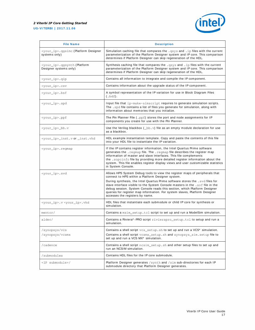
File Name Description
<your_ip>.qgsimc (Platform Designersystems only)
Simulation caching file that compares the .qsys and .ip files with the currentparameterization of the Platform Designer system and IP core. This comparisondetermines if Platform Designer can skip regeneration of the HDL.
<your_ip>.qgsynth (PlatformDesigner systems only)
Synthesis caching file that compares the .qsys and .ip files with the currentparameterization of the Platform Designer system and IP core. This comparisondetermines if Platform Designer can skip regeneration of the HDL.
<your_ip>.qip Contains all information to integrate and compile the IP component.
<your_ip>.csv Contains information about the upgrade status of the IP component.
<your_ip>.bsf A symbol representation of the IP variation for use in Block Diagram Files(.bdf).
<your_ip>.spd Input file that ip-make-simscript requires to generate simulation scripts.The .spd file contains a list of files you generate for simulation, along withinformation about memories that you initialize.
<your_ip>.ppf The Pin Planner File (.ppf) stores the port and node assignments for IPcomponents you create for use with the Pin Planner.
<your_ip>_bb.v Use the Verilog blackbox (_bb.v) file as an empty module declaration for useas a blackbox.
<your_ip>_inst.v or _inst.vhd HDL example instantiation template. Copy and paste the contents of this fileinto your HDL file to instantiate the IP variation.
<your_ip>.regmap If the IP contains register information, the Intel Quartus Prime softwaregenerates the .regmap file. The .regmap file describes the register mapinformation of master and slave interfaces. This file complementsthe .sopcinfo file by providing more detailed register information about thesystem. This file enables register display views and user customizable statisticsin System Console.
<your_ip>.svd Allows HPS System Debug tools to view the register maps of peripherals thatconnect to HPS within a Platform Designer system.During synthesis, the Intel Quartus Prime software stores the .svd files forslave interface visible to the System Console masters in the .sof file in thedebug session. System Console reads this section, which Platform Designerqueries for register map information. For system slaves, Platform Designeraccesses the registers by name.
<your_ip>.v <your_ip>.vhd HDL files that instantiate each submodule or child IP core for synthesis orsimulation.
mentor/ Contains a msim_setup.tcl script to set up and run a ModelSim simulation.
aldec/ Contains a Riviera*-PRO script rivierapro_setup.tcl to setup and run asimulation.
/synopsys/vcs
/synopsys/vcsmx
Contains a shell script vcs_setup.sh to set up and run a VCS* simulation.Contains a shell script vcsmx_setup.sh and synopsys_sim.setup file toset up and run a VCS MX* simulation.
/cadence Contains a shell script ncsim_setup.sh and other setup files to set up andrun an NCSIM simulation.
/submodules Contains HDL files for the IP core submodule.
<IP submodule>/ Platform Designer generates /synth and /sim sub-directories for each IPsubmodule directory that Platform Designer generates.
2 Viterbi IP Core Getting Started
UG-VITERBI | 2017.11.06
Viterbi IP Core User Guide17

2.4 Simulating Intel FPGA IP Cores
The Intel Quartus Prime software supports IP core RTL simulation in specific EDAsimulators. IP generation creates simulation files, including the functional simulationmodel, any testbench (or example design), and vendor-specific simulator setup scriptsfor each IP core. Use the functional simulation model and any testbench or exampledesign for simulation. IP generation output may also include scripts to compile and runany testbench. The scripts list all models or libraries you require to simulate your IPcore.
The Intel Quartus Prime software provides integration with many simulators andsupports multiple simulation flows, including your own scripted and custom simulationflows. Whichever flow you choose, IP core simulation involves the following steps:
1. Generate simulation model, testbench (or example design), and simulator setupscript files.
2. Set up your simulator environment and any simulation scripts.
3. Compile simulation model libraries.
4. Run your simulator.
2.5 DSP Builder for Intel FPGAs Design Flow
DSP Builder for Intel FPGAs shortens digital signal processing (DSP) design cycles byhelping you create the hardware representation of a DSP design in an algorithm-friendly development environment.
This IP core supports DSP Builder for Intel FPGAs. Use the DSP Builder for Intel FPGAsflow if you want to create a DSP Builder for Intel FPGAs model that includes an IP corevariation; use IP Catalog if you want to create an IP core variation that you caninstantiate manually in your design.
Related Links
Using MegaCore Functions chapter in the DSP Builder for Intel FPGAs Handbook.
2 Viterbi IP Core Getting Started
UG-VITERBI | 2017.11.06
Viterbi IP Core User Guide18

3 Viterbi IP Core Functional Description
3.1 Decoder
The Viterbi decoder can be a continuous or block decoder.
The continuous decoder processes a number of symbols greater than the tracebacklength. When the decoder traces back the number of bits (traceback length), itdelivers output bits. This behavior changes when you assert the end of packet (EOP)signal. The decoder then switches to block decoding, starting traceback from the lastsymbol or state. The tr_init_state signal indicates the end state that starts thetraceback operation. For block decoding Intel recommends you indicate the end stateof the tail bits (usually zero) and set the tb_type signal to 1.
3.2 Convolutional Encoder
The viterbi IP core convolutional encoder.
Figure 7. Convolutional EncoderL = 5, N = 2 and polynomials GA = 19 and GB = 29. GA in decimal is 19, which is equal to 10011 in binary.The most significant bit of the binary representation is the connection at the input data bit; the least significantbit (LSB) represents the connection at the end of the shift register chain. The XOR function implements themodulo-2 adding operation
RR Port
MSB
LSB
ga_xor
gb_xor
3.3 Trellis Coded Modulation
Trellis coded modulation (TCM) combines modulation and encoding processes toachieve better efficiency without increasing the bandwidth.
Bandwidth-constrained channels operate in the region R/W > 1, where R = data rateand W = bandwidth available. For such channels, digital communication systems usebandwidth efficient multilevel phase modulation. For example, phase shift keying(PSK), phase amplitude modulation (PAM), or quadrature amplitude modulation(QAM).
UG-VITERBI | 2017.11.06
Intel Corporation. All rights reserved. Intel, the Intel logo, Altera, Arria, Cyclone, Enpirion, MAX, Nios, Quartusand Stratix words and logos are trademarks of Intel Corporation or its subsidiaries in the U.S. and/or othercountries. Intel warrants performance of its FPGA and semiconductor products to current specifications inaccordance with Intel's standard warranty, but reserves the right to make changes to any products and servicesat any time without notice. Intel assumes no responsibility or liability arising out of the application or use of anyinformation, product, or service described herein except as expressly agreed to in writing by Intel. Intelcustomers are advised to obtain the latest version of device specifications before relying on any publishedinformation and before placing orders for products or services.*Other names and brands may be claimed as the property of others.
ISO9001:2008Registered

When you apply TCM to a bandwidth-constrained channel, you see a performance gainwithout expanding the signal bandwidth. An increase in the number of signal phasesfrom four to eight requires approximately 4dB in additional signal power to maintainthe same error rate. Hence, if TCM is to provide a benefit, the performance gain of therate 2/3 code must overcome this 4dB penalty. If the modulation is an integral part ofthe encoding process and is designed in conjunction with the code to increase theminimum Euclidian distance between the pairs of coded signals, the loss from theexpansion of the signal set is easily overcome and significant coding gain is achievedwith relatively simple codes.
Any bandwidth-constrained system benefits from this technique, for example, satellitemodem systems. The TCM Viterbi decoder only supports N = 2 (only mother coderates of 1/2).
3.3.1 Half-Rate Convolutional Codes
A 1/2 rate convolutional code encodes one information bit and leaves the secondinformation bit uncoded.
Figure 8. Half-Rate Convolutional CodeWith an eight-point signal constellation (e.g. eight-PSK), the two bits select one of the four subsets in thesignal constellation. The remaining information bit selects one of the two points within each subset.
Uncoded Bit
Input
c 2
c 0
GB
GA
c 1
3 Viterbi IP Core Functional Description
UG-VITERBI | 2017.11.06
Viterbi IP Core User Guide20

Figure 9. Mapping of Coded Bits and Sector Numbers
The specific mapping is not important. You can derive other mappings by permutating subsets in a way thatpreserves the main property of increased minimum distance among the subsets. However, you can create anyother mapping, including symbol mappings for 8-PSK, 16-PSK and others.
011001
000
110
111101
100
010
0
12
3
4
5 6
7
If you create another mapping, you must correctly connect the branch metrics createdoutside the IP core to the input ports and correctly configure the polynomials GA andGB for the trellis generation.
3 Viterbi IP Core Functional Description
UG-VITERBI | 2017.11.06
Viterbi IP Core User Guide21
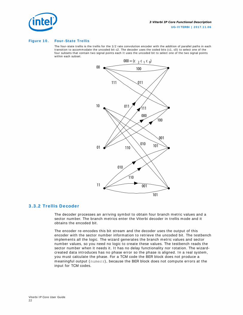
Figure 10. Four-State TrellisThe four-state trellis is the trellis for the 1/2 rate convolution encoder with the addition of parallel paths in eachtransition to accommodate the uncoded bit c2. The decoder uses the coded bits (c1, c0) to select one of thefour subsets that contain two signal points each It uses the uncoded bit to select one of the two signal pointswithin each subset.
00
01
10
11
101
001
110
010
000 = (c 2 c 1 c 0)
011111
111011
100
000100
001
101010110
3.3.2 Trellis Decoder
The decoder processes an arriving symbol to obtain four branch metric values and asector number. The branch metrics enter the Viterbi decoder in trellis mode and itobtains the encoded bit.
The encoder re-encodes this bit stream and the decoder uses the output of thisencoder with the sector number information to retrieve the uncoded bit. The testbenchimplements all the logic. The wizard generates the branch metric values and sectornumber values, so you need no logic to create these values. The testbench reads thesector number when it needs it. It has no delay functionality nor rotation. The wizard-created data introduces has no phase error so the phase is aligned. In a real system,you must calculate the phase. For a TCM code the BER block does not produce ameaningful output (numerr), because the BER block does not compute errors at theinput for TCM codes.
3 Viterbi IP Core Functional Description
UG-VITERBI | 2017.11.06
Viterbi IP Core User Guide22
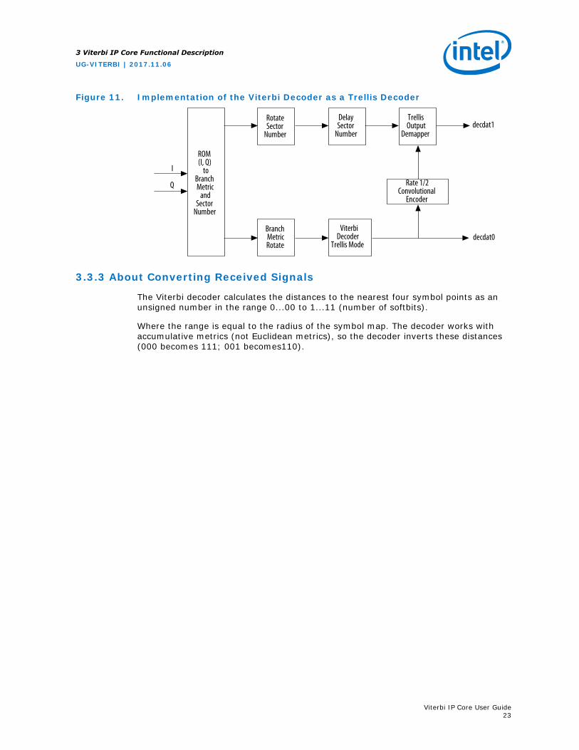
Figure 11. Implementation of the Viterbi Decoder as a Trellis Decoder
decdat0Viterbi
DecoderTrellis Mode
Rate 1/2Convolutional
Encoder
TrellisOutput
Demapperdecdat1
BranchMetricRotate
DelaySector
Number
ROM(I, Q)
toBranchMetric
andSector
Number
RotateSector
Number
I
Q
3.3.3 About Converting Received Signals
The Viterbi decoder calculates the distances to the nearest four symbol points as anunsigned number in the range 0...00 to 1...11 (number of softbits).
Where the range is equal to the radius of the symbol map. The decoder works withaccumulative metrics (not Euclidean metrics), so the decoder inverts these distances(000 becomes 111; 001 becomes110).
3 Viterbi IP Core Functional Description
UG-VITERBI | 2017.11.06
Viterbi IP Core User Guide23

Figure 12. Conversion of Received Symbol into Four Branch Metrics and a SectorNumber
Branch Metric 1
Branch Metric 3
Branch Metric 2
Branch Metric 0
Received Symbol
011
001
000
110
111
101
100
010
2
For example, consider a received symbol that lands in sector number 2 with thefollowing distances to the four nearest symbol map points:
• 1111
• 1101
• 1011
• 0001
Where the distance of the radius for 4 softbits is 1111. The distances are inverted toobtain the following branch metrics:
• Branch metric 0 = 0000
• Branch metric 1 = 0010
• Branch metric 2 = 0100
• Branch metric 3 = 1110
The decoder uses the coded bits (c1, c0) to select the branch metric number, which ituses to decide where to connect the branch metrics to the rr input of the Viterbidecoder. Branch metric 3 goes to the most significant bits (MSB) of rr; branch metric0 goes to the least significant bits (LSB) of rr.
3 Viterbi IP Core Functional Description
UG-VITERBI | 2017.11.06
Viterbi IP Core User Guide24

3.3.4 Trellis Termination
Block decoders must properly decode the last bits of the block and adapt to theconvolutional encoder.
Tail-biting feeds the convolutional encoder with a block and terminates it with (L – 1)unknown bits taken from the end of the block. Tail-biting sets the initial state of theconvolutional encoder with the last (L – 1) information bits. Tail-biting is decoded byreplicating the block at the decoder or double feeding the block into the decoder. Bydecoding in the middle point, the trellis is forced into the state that is both the initialstate and the end state. From the first decoding block, you can take the last half ofthe block; from the second decoded block (or second pass through the decoder), youcan obtain the first half of the bits of the block.
Note: In tail-biting, the block size must be large enough to train the decoder, otherwise youmay see BER loss.
Alternatively, if you initialize the convolutional encoder to zero, the initial state of thetrellis is zero. The decoder knows the last (L – 1) bits to the convolutional encoder.They bring the convolutional encoder to a known end state. The decoder then usesthis information to set the end state of the trellis with tr_init_state, which isderived from the last (L – 1) bits of the block in reverse order. For example, for ablock that ends in: ...000101 If L = 5 and the decoder knows the last (L – 1) = 4 bits,it sets tr_init_state as 0101, which reversed and in binary is 1010, or 10 indecimal. The wizard generates tr_init_state as if it knows the last (L – 1) bits ofeach block.
3.3.5 Trellis Initialization
The parallel decoder always starts its trellis from state zero for a new block.
However, the hybrid decoder allows you to set the initial state (usually zero) withbm_init_state. This signal ranges from 0 to 2 (L – 1) – 1, which are the trellisstates. The bm_init_value signal initializes the state metric of the state indicated bybm_init_state. The decoder initializes all other states with zero. The appropriatevalue for this port is approximately 2(bmgwide – 2) or any value between 2(N + softbits) to2(bmgwide – 1). Continuous decoders never reset the state metrics, which creates apossible difference if the same block of data is sent several times. Initially, thedecoder sets the state metrics so that the state metric for state 0 is 0, and all othersinfinity. For any subsequent blocks, the state metrics contain whatever they havewhen the previous block ends.
3.4 Viterbi IP Core Parameters
3.4.1 Architecture
3 Viterbi IP Core Functional Description
UG-VITERBI | 2017.11.06
Viterbi IP Core User Guide25

Table 7. Architecture Parameters
Parameter Value Description
Viterbi architecure Hybrid or Parallel Selects the hybrid or parallel architecture.
BER On or Off Specifies the BER estimator option, refer to “BER Estimator” on page 3–7.
Node Sync On or Off Specifies the node synchronization option (only available when BERoption is on).
Optimizations None, Continuous, or Block Specifies the optimization for the parallel decoder. if you select Noneyou can turn on Best State Finder. However, to use less logic, turn offBest State Finder.
3.4.1.1 BER Estimator
The BER estimator option uses a re-encode and compare approach for estimating thenumber of errors in the input data.
Figure 13. BER Block Diagram
ViterbiDecoder
Input Symbols
Delay
Compareand Count
BER Output(numerr)
ConvolutionalEncoder
In cases where the signal-to-noise ratio is sufficiently high to allow the decoder todecode an error-free output, the BER estimation is very close to the actual channelBER. When the decoder is not decoding an error-free output, the estimated BER ishigher and more random than the actual channel BER, which introduces a degree ofuncertainty directly proportional to the output errors.
Note: For a TCM code, the BER block does not produce a meaningful output (numerr)because the BER block does not compute errors at the input for TCM codes.
3 Viterbi IP Core Functional Description
UG-VITERBI | 2017.11.06
Viterbi IP Core User Guide26

Figure 14. Graph Comparing Actual BER with Estimated BER
3.00 3.50 4.00 4.50 5.00 5.50 6.00Signal-to-Noise Ratio
BER
Actual BEREstimated BER
1.00e-03
1.00e-02
1.00e-01
3.4.1.2 Node Synchronization
If you are not using external synchronization, you may not know the order of your Nbits. The node synchronization option allows you to rotate the rr inputs until thedecoder is in synchronization. To use node synchronization, you observe the BER andkeep changing state_node_sync to rotate the rr inputs until you get the correct valuefor the BER.
Figure 15. Node Synchronization Block Diagram
state_node_sync
BarrelRotator
rr(1)rr(2)
...
RR(1)RR(2)...
rr(N) RR(N)
The following equation represents node synchronization:
RR[i] = rr[((state_node_sync + i – 1) mod N) + 1]
where i is 1 to N.
RR and rr are treated as an array of width N of busses softbits wide. The range ofvalid values for state_node_sync is 0 to (N – 1).
3 Viterbi IP Core Functional Description
UG-VITERBI | 2017.11.06
Viterbi IP Core User Guide27

3.4.2 Code Sets
Table 8. Code Sets Parameters
Parameter Value Description
Number of CodeSets
1 to 8 The Viterbi IP core supports multiple code definitions. The multiple code setoption allows up to eight code sets, where a code set comprises a code rate andassociated generating polynomials.
Number of codedbits. (N)
2 to 7 (hybrid)2 to 4 (parallel)
For every bit to be encoded, N bits are output. With the multiple code set optionthere are up to 5 different N parameters, which can be in any order. Valid onlyfor Viterbi mode. For TCM mode only N = 2 is supported
Constraint length(L)
3 to 9 The constraint length. Defines the number of states in the convolutional encoder,where number of states = 2(L – 1). You can choose different values of L for eachcode set.
Decimal or Octal – Decimal or octal base representation for the generator polynomials. The designfile representation is decimal, but you have the option of entering in eitherdecimal or octal base.
Mode V or T Viterbi (V) or TCM mode (T).
GA, GB, GC, GD,GE, GF, GG
– The generator polynomials. If you use the multiple code set option, the wizardenters a different set of polynomials in the respective gi group. The wizardprovides default values that you can overwritte by any valid polynomial. (Thewizard does not check whether the entered values are valid.) The parallelarchitecture uses only GA, GB, GC, and GD.
For multiple code sets, the first code definition corresponds to the first line and isselected with sel_code input = 0; the second line is selected with sel_code = 1;the third with sel_code = 2 and so on. For each code definition you can select N, thepolynomials, the constraint length L, and the mode (Viterbi or TCM). You can mixdifferent constraint lengths with different TCM and Viterbi modes. The test data, whichthe wizardr creates, tests each of the code definitions. You can see these tests in thesimulation with the testbench or if you look at the block_period_stim.txt file.
In hybrid mode, for constraint lengths of 3 and 4, the bitwidth of tr_init_state is4, but the MegaCore function ignores the redundant higher bits.
For multiple constraint lengths, some of the last decoded bits may be incorrect,becauset of the Viterbi algorithm. To avoid this effect, give a lower BER, and reducethe probability of being on the wrong trellis path, set Optimization to None and turnon Best State Finder.
3.4.3 Viterbi Parameters
Parameter Value Description
Maximumconstraint length(LMAX)
5 to 9 (hybrid)3 to 9 (parallel)
The maximum constraint length LMAX. .
ACS Units (A) 1, 2, 4, 8, or 16 The number of ACS units, which adds a degree of parallelism (hybrid architectureonly). The range of values available depends upon the value of maximumconstraint length LMAX.
continued...
3 Viterbi IP Core Functional Description
UG-VITERBI | 2017.11.06
Viterbi IP Core User Guide28

Parameter Value Description
Traceback (v) 8 (minimum) The traceback length, which is the number of stages in the trellis that are tracedback to obtain a decoded bit. It is typically set to 6 × L for unpunctured codes, andup to 15 × L for highly punctured codes.
Softbits (softbits) 1 to 16 The number of soft decision bits per symbol. When softbits is set to 1 bit, thedecoder acts as a hard decision decoder, and still allows for erased symbols to beentered using the eras_sym input.
Bmgwide – The precision of the state metric accumulation. The parameter editor selects anddisplays the optimum value, which depends on NMAX, LMAX and, softbits.
3.4.3.1 Soft Symbol Input
The number of soft decision bits per symbol, softbits, represent 2softbits – 1 soft 0s and2softbits – 1 soft 1s. The input values represent received signal amplitudes. If the inputis in log-likelihood format, a transformation is required and you must use extrasoftbits to retain signal integrity. The decoder marks depunctured values separately.The decoder allows a hard-decision input when softbits = 1.
Table 9. Soft Symbol Input Representationsoftbits = 3
Soft Symbol Meaning
011 Strongest '0'
010 Strong '0'
001 Weak '0'
000 Weakest '0'
111 Weakest '1'
110 Weak '1'
101 Strong '1'
100 Strongest '1'
3.4.3.2 State Metrics
The Viterbi decoder state metrics are accumulative not Euclidean and are based onmaximum metrics rather than minimum metrics.
As the metrics grow, normalize them to avoid overflow. When a normalization occursthe decoder subtracts 2(bmgwide – 1) from all metrics and increases the normalizationregister by +1. The total metric value for the best path = (number of normalizations)× (2(bmgwide – 1)) + bestmet. The total metric value for the best path, the number ofsymbols processed, and the number of errors in the BER block indicate the quality ofthe channel and whether you have a suitable value for softbits. The output bestaddindicates the state that has the best metric.
3.4.3.3 Throughput Calculator
3 Viterbi IP Core Functional Description
UG-VITERBI | 2017.11.06
Viterbi IP Core User Guide29
The throughput calculator uses the following equation:
Hybrid throughput = fMAX/Z
where:
• — Z = 10, if log2C = 3
— Z= 2log2C, if log2C > 3
— log2C = LMAX – 2 – log2A
— LMAX is the maximum constraint length
— A is ACS units
— Parallel throughput = fMAX
3.4.3.4 Latency Calculator
The latency calculator gives you an approximate indication of the latency of yourViterbi decoder.
Latency is the number of clock cycles it takes the decoder to process r the data andoutput it. Latency is from the first symbol to enter the IP core (sink_sop) up to thefirst symbol to leave (source_sop). The latency depends on the parameters. For theprecise latency, perform simulation. The latency calculator uses the following formulafor the hybrid architecture:
Number of clock cycles = Z × V
where:
• — V is the traceback length value that is in the input tb_length
— Z = 10, if log2C = 3
— Z = 2log2C, if log2C > 3
— log2C = LMAX – 2 – log2A, where A is ACS units
For the parallel architecture the number of clock cycles is approximately 4V.
3.4.4 Test Data
Parameter Description
Number of bits per block The number of bits per block.The number of bits per block × the number of blocks must be less than50,000,000.
Signal to noise ratio (dB) The signal to noise ratio, which must be between 1 and 100.
Number of blocks The number of blocks.The number of bits per block × the number of blocks must be less than50,000,000.
Pattern A Enter the puncturing pattern A.
Pattern B Enter the puncturing pattern B.
3 Viterbi IP Core Functional Description
UG-VITERBI | 2017.11.06
Viterbi IP Core User Guide30

3.4.4.1 External Puncturing
Both parallel and hybrid architectures support external puncturing.
All punctured codes are based on a mother code of rate 1/2. For external depuncturingyou must depuncture the received data stream external to the decoder and input thedata into the decoder n symbols at a time.
Table 10. Puncturing SchemesYou can define these schemes and their rate. CA refers to the most significant (first transmitted bit, firstreceived symbol); CB refers to the least significant (last transmitted bit, last received symbol)
Punctured Rate Puncturing Scheme
Bit Multiplier
2/3 CA 1 0
CB 1 1
3/4 CA 1 0 1
CB 1 1 0
4/5 CA 1 0 0 0
CB 1 1 1 1
5/6 CA 1 0 1 0 1
CB 1 1 0 1 0
6/7 CA 1 0 0 1 0 1
CB 1 1 1 0 1 0
7/8 CA 1 1 1 1 0 1 0
CB 1 0 0 0 1 0 1
3.5 Viterbi IP Core Interfaces and Signals
The Viterbi Avalon-ST interface supports backpressure, which is a flow controlmechanism, where a sink can indicate to a source to stop sending data.
The ready latency on the Avalon-ST input interface is 1.
You may achieve a higher clock rate by driving the source ready signal source_rdyof the Viterbi high, and not connecting the sink ready signal sink_rdy.
3.5.1 Avalon-ST Interfaces in DSP IP Cores
Avalon-ST interfaces define a standard, flexible, and modular protocol for datatransfers from a source interface to a sink interface.
The input interface is an Avalon-ST sink and the output interface is an Avalon-STsource. The Avalon-ST interface supports packet transfers with packets interleavedacross multiple channels.
Avalon-ST interface signals can describe traditional streaming interfaces supporting asingle stream of data without knowledge of channels or packet boundaries. Suchinterfaces typically contain data, ready, and valid signals. Avalon-ST interfaces canalso support more complex protocols for burst and packet transfers with packets
3 Viterbi IP Core Functional Description
UG-VITERBI | 2017.11.06
Viterbi IP Core User Guide31
interleaved across multiple channels. The Avalon-ST interface inherently synchronizesmultichannel designs, which allows you to achieve efficient, time-multiplexedimplementations without having to implement complex control logic.
Avalon-ST interfaces support backpressure, which is a flow control mechanism wherea sink can signal to a source to stop sending data. The sink typically usesbackpressure to stop the flow of data when its FIFO buffers are full or when it hascongestion on its output.
Related Links
Avalon Interface Specifications
3.5.2 Global Signals
Signal Name Description
clk The main system clock. The whole MegaCore function operates on the rising edge of clk.
reset Reset. The entire decoder is asynchronously reset when reset is asserted high. The reset signal resets theentire system. You must deassert the reset signal synchronously with respect to the rising edge of clk.
3.5.3 Avalon-ST Sink Signals
Signal Name Avalon-STName
Direction Description
eras_sym[Nmax:1]
dat Input When asserted, eras_sym Indicates an erased symbol. Both rr anderas_sym are Avalon-ST dat inputs
rr dat Input Data input, which takes in n symbols, each softbits wide per clock. InTCM mode the rr width is (2N × softbits:1); in Viterbi mode the rrwidth is (nmax × softbits:1).Both rr and eras_sym are Avalon-STdat inputs
sink_eop eop Input End of packet (block) signal. sink_eop delineates the packetboundaries on the rr bus. When sink_eop is high, the end of thepacket is present on the dat bus. sink_eop is asserted on the lasttransfer of every packet. This signal applies to block decoding only.
sink_rdy ready Output Data transfer enable signal.The interface sink drives sink_rdy andcontrols the flow of data across the interface. sink_rdy behaves asa read enable from sink to source. When the source observessink_rdy asserted on the clk rising edge, it can drive the Avalon-ST data interface signals and assert sink_val as early as the nextclock cycle, if data is available. In the hybrid architecture, sink_rdyis asserted for one clock cycle at a time. If data is not available atthe time, you have to wait for the next sink_rdy pulse.
sink_sop sop Input Start of packet (block) signal. sop delineates the packet boundarieson the rr bus. When sink_sop is high, the start of the packet ispresent on the rr bus. sink_sop is asserted on the first transfer ofevery packet This signal applies to block decoding only.
sink_val val Input Data valid signal. sink_val indicates the validity of the datasignals. sink_val is updated on every clock edge where sink_rdyis sampled asserted, and holds its current value along with the dat
continued...
3 Viterbi IP Core Functional Description
UG-VITERBI | 2017.11.06
Viterbi IP Core User Guide32

Signal Name Avalon-STName
Direction Description
bus where sink_rdy is sampled deasserted. When sink_val isasserted, the Avalon-ST data interface signals are valid. Whensink_val is deasserted, the Avalon-ST data interface signals areinvalid and you must disregard them. To determine whether newdata has been received, the sink qualifies the sink_val signal withthe previous state of the sink_rdy signal.
sink_data data Input In Qsys systems, this Avalon-ST-compliant data bus includes all theAvalon-ST input data and configuration signals. The signals are in thefollowing order from MSB to LSB:• In
• State_node_sync
• Ber_clear
• Sel_code
• Tb_type
• Tb_length
• Tr_init_state
• Bm_init_state
• Bm_init_value
• Eras_symRr
3.5.4 Avalon Source-ST Signals
Signal Avalon-STName
Direction Description
decbit dat Output The decbit signal contains output bits when source_val is asserted.
source_eop eop Output End of packet (block) signal. if you select continuous optimization,this signal is left open and you must remove it from the testbench.
source_rdy ready Input Data transfer enable signal. The sink interface drives source_rdyand uses it to control the flow of data across the interface. enabehaves as a read enable from sink to source. When the sourceobserves source_rdy asserted on the clk rising edge it drives, onthe following clk rising edge, the Avalon-ST data interface signalsand asserts source_val. The sink captures the data interfacesignals on the following clk rising edge. If the source is unable toprovide new data, it deasserts source_val for one or more clockcycles until it is prepared to drive valid data interface signals.
source_sop sop Output Start of packet (block) signal. if you select continuous optimization,this signal is left open and you must remove it from the testbench.
source_val val Output Data valid signal. The IP core assers source_val high for one clockcycle, whenever there is a valid output on the decbit signal.
out_data data Output In Qsys systems, this Avalon-ST-compliant data bus includes all theAvalon-ST output data and configuration signals. The signals are inthe following order from MSB to LSB:• Numerr
• BestAdd
• BestMet
• Normalizations
• Decbit
3 Viterbi IP Core Functional Description
UG-VITERBI | 2017.11.06
Viterbi IP Core User Guide33

3.5.5 Configuration Signals
Signal Name Description
ber_clear Reset for the BER counter. Only for the BER block option.
bm_init_state[(L-1):1] Specifies the state in which to initialize with the value from thebm_init_value[] bus. All other state metrics are set to zero. the IP corelatches bm_init_state when sink_sop is asserted. Hybrid architecture only.
bm_init_value[(L-1):1] Specifies the value of the metric that initializes the start state. All other metricsare set to 0. bm_init_value must be larger than (L × 2(softbits – 1)). the IP corelatches bm_init_value when sink_sop is asserted. Hybrid architecture only.
sel_code[log2(Ncodes):1] Selects the codeword. ’0’ selects the first codeword, ‘1’ selects the second, andso on. The bus size increases according to the number of codes specified. The IPcore latches sel_code when sink_sop is asserted.
state_node_sync[log2(Nmax):1] Specifies the node synchronization rotation to rr.The IP core latches state_node_sync signal when sink_sop is asserted.Available only when you turn on Node Sync.
tb_length[] Traceback length. The maximum width of tb_length is equal to the maximumvalue of parameter v. The IP core latches tb_length input when sink_sop isasserted. This IP core disables this signal if you select the continuousoptimization: you must then remove it from the testbench. Not available forparallel architectures with block optimization.
tb_type Parallel architectures only. Altera recommends that you set tb_type high alwaysfor future compatibility. In block decoding when tb_type is low, the decoderstarts from state 0; when tb_type is high, the decoder uses the state specifiedin tr_init_state[(L-1):1]. For block decoding set tb_type high. The IPcore latches tb_type when sink_eop is asserted. If you select None orContinuous optimization, the IP core connects this input to zero.
tr_init_state[(L-1):1] Specifies the state to start the traceback from, when tb_type is asserted high.The IP core latches tr_init_state when sink_eop is asserted. If you selectcontinuous optimization, this input is removed from the top level design andconnected to zero in the inner core.
3.5.6 Status Signals
3 Viterbi IP Core Functional Description
UG-VITERBI | 2017.11.06
Viterbi IP Core User Guide34

Signal Description
bestadd[(L-1):1] The best address state. The address corresponding to the best metric as it isbeing found by the best state finder. The metric of this state if shown inbestmet. If you select Continuous or None optimization and turn off best statefinder, the IP core leaves this signal open. For parallel decoders, the IP coreremoves this signal.
bestmet[bmgwide:1] The best metric. The bestmet signal shows the best state metric for every trellisstep as the best state finder finds it. The state that contains this best metric isshown in bestadd. If you select Continuous or None for optimization and turnoff best state finder, the IP core leave this signal open, For parallel decoders, theIP core removes this signal.
normalizations[8:1] The normalizations bus indicates in real time the number of normalizations thatoccur since you activated sink_sop.
numerr[] The numerr bus contains the number of errors detected during a block. The iPcore updates it each time it detects an error, so you can see the location ofindividual errors. It is reset when source_sop asserted; it is valid two-clockcycles after source_sop. The wizard automatically sets the width of this bus. Ifyou do not select a BER block, the IP cores leaves this signal open. Onlyavailable when you select the BER estimator option
3.5.7 Viterbi IP Core Timing Diagrams
Figure 16. Hybrid Decoder Input Timing DiagramThe sink_rdy signal is asserted for one clock cycle in every Z clock cycles. If the decoder becomes fullbecause data is not being collected on the source side, it may deassert sink_rdy until it can accept new data.The decoder only accepts data, if sink_rdy is asserted.
clksink_rdysink_val
sink_sopsink_eop
rr[8:1] 77 8888
Figure 17. Parallel Decoder Input Timing Diagram
clksink_rdysink_val
sink_sopsink_eop
rr[8:1] valid data valid data
3 Viterbi IP Core Functional Description
UG-VITERBI | 2017.11.06
Viterbi IP Core User Guide35

Figure 18. Output Timing - Example 1The source_val signal is asserted initially for 8 or 16 clock cycles. It is then asserted for the number of clockcycles corresponding to the amount of remaining data, if source_rdy remains asserted. The typical ending ofa block or packet in the Avalon-ST interface is on the source (Viterbi) to the sink (user) side connection.
clksource_sopsource_eopsource_rdysource_val
decbit
Figure 19. Output Timing - Example 2With a different ending.
clksource_sopsource_eopsource_rdy
source_valdecbit
Figure 20. Depuncturing Timing DiagramThis depuncturing timing diagram shows eras_sym for the pattern 110110 (puncturing rate 3/4). By changingthe eras_sym pattern you can implement virtually any depuncturing pattern you require.
clkenaval
soprr[8:5]rr[4:1]
eras_sym[2]eras_sym[1]
B X 7 A X 7
8 7 X D 9 X
3 Viterbi IP Core Functional Description
UG-VITERBI | 2017.11.06
Viterbi IP Core User Guide36

A Viterbi IP Core User Guide Document ArchivesIf an IP core version is not listed, the user guide for the previous IP core version applies.
IP Core Version User Guide
15.0 Viterbi IP Core User Guide v15.0
14.1 Viterbi IP Core User Guide v14.1
UG-VITERBI | 2017.11.06
Intel Corporation. All rights reserved. Intel, the Intel logo, Altera, Arria, Cyclone, Enpirion, MAX, Nios, Quartusand Stratix words and logos are trademarks of Intel Corporation or its subsidiaries in the U.S. and/or othercountries. Intel warrants performance of its FPGA and semiconductor products to current specifications inaccordance with Intel's standard warranty, but reserves the right to make changes to any products and servicesat any time without notice. Intel assumes no responsibility or liability arising out of the application or use of anyinformation, product, or service described herein except as expressly agreed to in writing by Intel. Intelcustomers are advised to obtain the latest version of device specifications before relying on any publishedinformation and before placing orders for products or services.*Other names and brands may be claimed as the property of others.
ISO9001:2008Registered

5 Document Revision HistoryViterbi IP Core User Guide revision history.
Date Version Changes
November 2017 2017.11.06 • Changed descriptions of tb_type and tb_lengthsignals
• Removed product ID and vendor ID.• Added support for Intel Cyclone 10 devices
2014.12.15 14.1 • Removed Arria 10 specific wizard comments• Added final support for Arria 10 and MAX 10 devices
August 2014 14.0 Arria 10 Edition • Added support for Arria 10 devices.• Added new sink_data and out_data bus description.• Added Arria 10 generated files description.• Removed table with generated file descriptions.
June 2014 14.0 • Removed support for Cyclone III and Stratix III devices.• Added support for MAX 10 FPGAs• Added instructions for using IP Catalog
November 2013 13.1 • Removed support for the following devices:• — Arria
— Cyclone II— HardCopy® II— HardCopy III— HardCopy IV— Stratix— Stratix II— Stratix GX— Stratix II GX
• Added full support for the following devices:• — Arria V
— Stratix V
November 2012 12.1 Added support for Arria V GZ devices.
May 2011 11.0 • Updated support level to final support for Arria II GX,Arria II GZ, Cyclone III LS, and Cyclone IV GX devices.
• Updated support level to HardCopy Compilation forHardCopy III, HardCopy IV E, and HardCopy IV GXdevices
.
December 2010 10.1 • Added preliminary support for Arria II GZ devices.• Updated support level to final support for Stratix IV GT
devices.
July 2010 10.0 Added preliminary support for Stratix V devices.
UG-VITERBI | 2017.11.06
Intel Corporation. All rights reserved. Intel, the Intel logo, Altera, Arria, Cyclone, Enpirion, MAX, Nios, Quartusand Stratix words and logos are trademarks of Intel Corporation or its subsidiaries in the U.S. and/or othercountries. Intel warrants performance of its FPGA and semiconductor products to current specifications inaccordance with Intel's standard warranty, but reserves the right to make changes to any products and servicesat any time without notice. Intel assumes no responsibility or liability arising out of the application or use of anyinformation, product, or service described herein except as expressly agreed to in writing by Intel. Intelcustomers are advised to obtain the latest version of device specifications before relying on any publishedinformation and before placing orders for products or services.*Other names and brands may be claimed as the property of others.
ISO9001:2008Registered