Visible Light Communication - University of Central Florida
133
i Visible Light Communication An alternative to the wireless transmission with RF spectrums through visible light communication. University of Central Florida Department of Electrical Engineering and Computer Science EEL 4915 Dr. Lei Wei, Dr. Samuel Richie, Dr. David Hagen Senior Design II Final Paper Documentation Group 12 – CREOL Garrett Bennett Photonic Science and Engineering Benjamin Stuart Photonic Science and Engineering George Salinas Computer Engineering Zhitao Chen Electrical Engineering
Transcript of Visible Light Communication - University of Central Florida

i
Visible Light Communication
An alternative to the wireless transmission with RF spectrums through visible light communication.
University of Central Florida Department of Electrical Engineering and Computer Science
EEL 4915
Dr. Lei Wei, Dr. Samuel Richie, Dr. David Hagen Senior Design II
Final Paper Documentation
Group 12 – CREOL
Garrett Bennett Photonic Science and Engineering Benjamin Stuart Photonic Science and Engineering George Salinas Computer Engineering Zhitao Chen Electrical Engineering

ii
Table of Contents
1. Executive Summary 1
2. Project Description 3
2.1 Project Background 3
2.1.1 Existing Projects and Products 3
2.1.2 Wireless Optical Communication 6
2.2 Objectives 7
2.2.1 Motivation 7
2.2.2 Goals 8
2.3 Requirements Specifications 8
2.4 Market and Engineering Requirements 8
2.5 Distribution and Hierarchical Layout 10
2.5.1 Contribution Breakdown 11
2.6 Design Comparison 11
3. Research related to Project 13
3.1 Relevant Technologies 13
3.1.1 Transmitter Technology 13
3.1.2 Receiver Technology 23
3.1.3 Detection Statistics 28
3.1.4 Electrical Processing 29
3.2 Strategic Components and Part Selections 30
3.2.1 Differential Receiver Amplifier 30
3.2.2 Operational Amplifier 34
3.2.3 Differential Driver 38
3.2.4 Comparator 40
3.2.5 Voltage Converters 42
3.2.6 LED 46
3.2.7 Photodiode 47
3.2.8 Laser Criteria 48
3.2.9 Focusing Optics 51

iii
4. Related Standards and Realistic Design Constraints 54
4.1 Standards 54
4.1.1 IEEE 802.3i 54
4.1.2 Design Impact of IEEE 802.3i standard 54
4.1.3 IEEE 802.15.7 55
4.1.4 Design Impact of IEEE 802.15.7 55
4.1.5 UL 1310 55
4.1.6 Design Impact of UL 1310 56
4.1.7 RoHS 56
4.1.8 Design Impact of RoHS 56
4.1.9 Power Supply Standards 56
4.1.10 PCB Standards 58
4.1.11 Design Impact of PCB standards 58
4.1.12 Laser Safety Standards 58
4.1.14 Software Standards C++ 59
4.1.15 Design Impact of C++ Standard 59
4.1.16 Electronics Housing Standards 60
4.1.17 Design Impact of Housing Standard 60
4.2 Design Constraints 60
4.2.1 Economic and Time Constraints 60
4.2.2 Environmental, Health and Safety Constraints 61
4.2.3 Environmental Spectral Window Distribution 61
4.2.4 Social, Political, and Ethical Constraints 62
4.2.5 Manufacturability and Sustainability Constraints 63
4.3 LAN (Local Area Network) 63
4.3.1 Full Duplex and Half Duplex Operation 64
4.3.2 Carrier Sense Multiple Access with Collision Detection (CSMA/CD) 64
4.3.2 Hubs and Switches 66
5 Project Hardware Design Details 68
5.1 Transmitter System Model 68
5.2 Transmitting Driver Background 69
5.2.1 White LED Modulation Background 70
iv
5.3 LED Driver 70
5.3.1 Laser Ethernet Transmitter Design 72
5.3.2 Transmitter Component Layout 72
5.3 Receiver System Model 74
5.3.1 Receiver Components 74
5.3.2 Receiver Layout 74
5.4 LAN Connectors 75
5.5 Power Supply 76
5.6 Device Housing 78
6. Project Software Design Details 79
6.1 Objective 79
6.1.1 Analysis 80
6.1.2 Software Development 80
6.1.3 Software Reutilization 81
6.2 Program Information and Overview 81
6.2.1 TCP/IP Protocol 81
6.2.2 Network Layer 82
6.2.3 Internet Layer 82
6.2.4 Transport Layer 82
6.2.5 Application Layer 82
6.2.6 IP (Internet Protocol) 83
6.3 Integrated Development Environment & Features to Develop 83
6.3.1 ICMP (Internet Control Message Protocol) 83
6.3.2 UDP (User Datagram Protocol) 83
6.3.3 TCP (Transmission Control Protocol) 84
6.3.4 Ethernet and TCP/IP Relationship 84
6.4 Software Flowchart 84
6.4.1 Program Implementation - Packet Generator 85
6.4.2 Class Diagram 86
6.5 Application of HTI (Human and Technology Interaction) 87
6.6 Software Testing 88
6.6.2 Unit Testing 88

v
6.6.2 Integration Testing 88
6.6.3 System Testing 88
6.6.4 Acceptance Testing 88
6.7 GUI Interface Development 88
6.7.1 Software Connection 89
6.7.2 Language Selection 90
6.7.3 PING Testing 91
6.7.4 TCP/IP Client-Server 92
6.7.5 Network Information Terminal 96
6.8 General Software Conclusion 99
7. Physical Testing and Prototype Construction 100
7.1 Testing Conditions 100
7.2 Transmitter Components 101
7.3 Receiver Components 103
7.4 VLC System 104
8. Project Construction 107
8.1 Printed Circuit Boards 107
8.2 Soldering 110
8.3 PCB assembly 112
9. Administrative Content 116
9.1 Budgeting 119
10. Concluding Remarks 120
Appendix A - Copyright Permissions 121
Appendix B – References 123
Appendix C – Miscellaneous 124

vi
Table of Figures Figure 2.1. The Vialight communication system as depicted from an aerial view. ........................... 4
Figure 2.2. The Lifi-X Dongle as produced by PureLifi for their 2017 product release. .................... 6
Figure 2.3. The house of quality of the system specifications. ........................................................... 9
Figure 2.4 The project distribution and hierarchical layout. ............................................................11
Figure 3.1: A visual representation of the band structures of three different kinds of elements..14
Below the physical illustration is a band-diagram representation, normally the valence and
conduction bands between the n-type and p-type are far apart respectively, however biasing with
voltage shifts them closer. ..................................................................................................................14
Figure 3.2: The figure illustrates the process of biasing an LED .......................................................14
Figure 3.3 A generalized illustration of what a laser diode might look like. ....................................17
Figure 3.4. A diagram showing a laser diode being used as a transmitter, its beam diverges by and
angle θ over the length L, a lens is placed at that length to intercept the beam and focus onto a
receiver. ...............................................................................................................................................17
Figure 3.5. The optical power to current graph, displaying the bias current point and the threshold
current dependence on temperature. ...............................................................................................18
Figure 3.6: An 8P8C connector ...........................................................................................................19
Figure 3.8. A graphical representation of TDM .................................................................................21
Figure 3.9. A graphical representation of FDM .................................................................................22
Figure 3.10. An approximate representation of multipath and MIMO ............................................22
Figure 3.11. A photoconductor illuminated with filtered white light. .............................................24
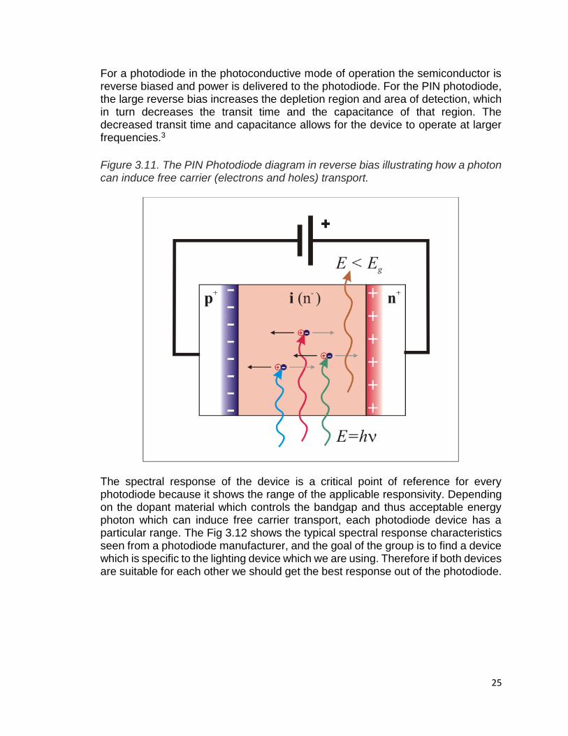
Figure 3.11. The PIN Photodiode diagram in reverse bias illustrating how a photon can induce free
carrier (electrons and holes) transport. .............................................................................................25
Figure 3.12. The spectral response of typical Hamamatsu corporation fast speed photodiodes. .26
Figure 3.13. The I-P curve for a typical background light on a PIN and LED illumination to determine
the reverse bias current and dynamic range. ....................................................................................27
Figure 3.14. The relative output of a square wave white LED at 10 Khz for a phototransistor in
orange and a photodiode in blue. ......................................................................................................27
Figure 3.15. The high-speed photodiode circuit (Courtesy of Hamamatsu). ..................................29
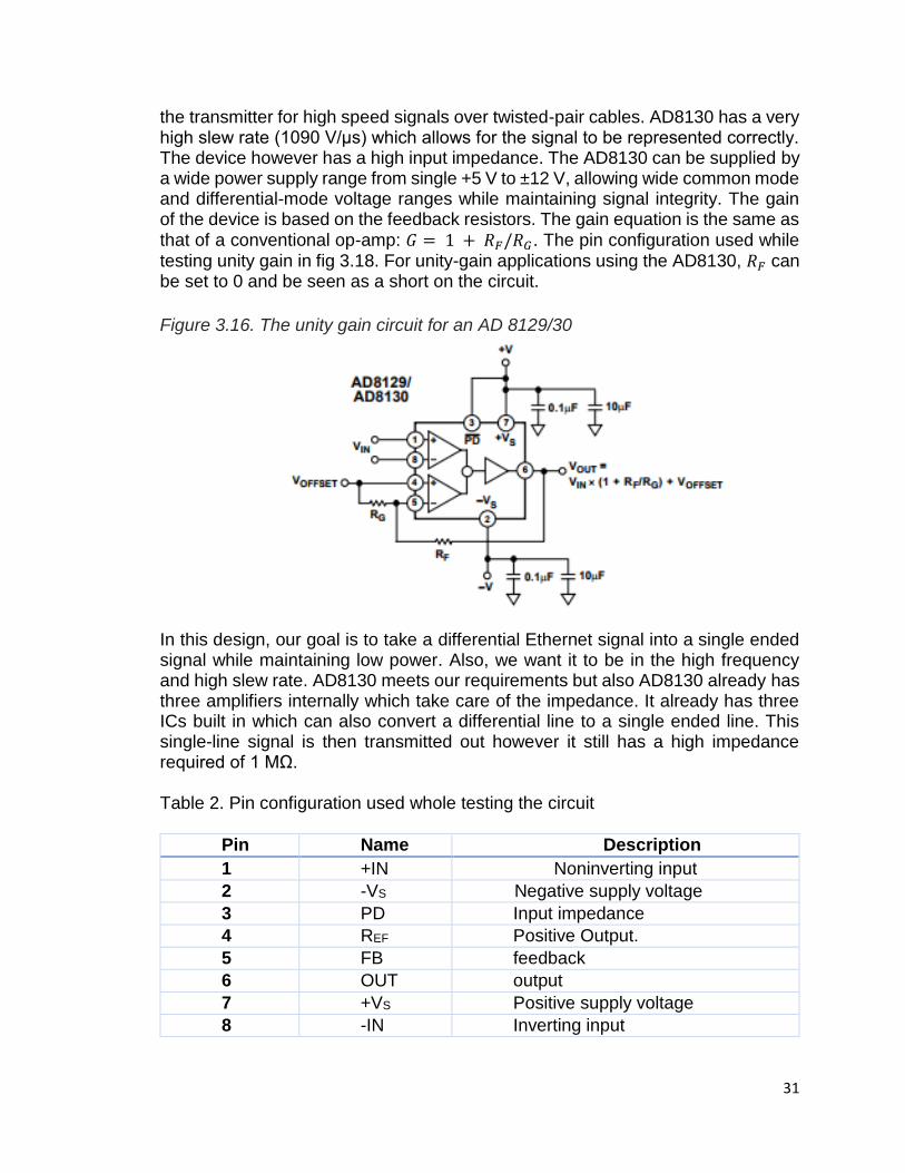
Figure 3.16. The unity gain circuit for an AD 8129/30 ......................................................................31
Figure 3.17 The Opticstudio design of an uncoated N-BK7 plano-convex lens optimized for RMS
spot size at 0,1º,-1º incidence angle at 650 nm. ...............................................................................52
Fig. 3.18 An aspheric lens (Courtesy of Edmund optics) ...................................................................53
Figure 4.2. The attenuation coefficient as a function of wavelength. .............................................62
Figure 4.3 Hierarchical LAN data transfer. .........................................................................................63
Figure 4.4. Data collision framework for half-duplex functionality. .................................................64
Figure 4.5. Hub and Switch behavior in multiple connections. ........................................................66
Figure 5.1. Ethernet Connected 10Base-T VLC Transceiver device from “Foundations of Visible
Light Communication Circuits” Prototype Design Premise. .............................................................69
Figure 5.3. The quiescent point of bias for an LED in terms of IV and relative light output vs current
(Courtesy of Lumileds). .......................................................................................................................70
vii
Figure 5.2. The MAX3967A recommended reference diagram (Courtesy of Maxim Integrated). .71
Figure 5.4 The NI Multisim configuration of the transmitter circuit. ...............................................73
Figure 5.5 The KiCad configuration of the transmitter circuit. .........................................................73
Figure 5.6 The KiCad configuration of the receiver circuit. ..............................................................75
Figure 5.7. Ethernet RJ-45 connector HY 911103A pin configurations. TX+(PIN1), TX-(PIN2),
CT(PIN3), CT(PIN4), GND(PIN5), GND(PIN6), RX+(PIN7), RX-(PIN8). ................................................75
Figure 5.8 Ethernet RJ-45 connector RJHSE 5380, and associated PCB layout. ..............................76
Figure 5.9 The KiCad configuration of the power supply circuit. .....................................................77
Figure 5.10 The housing complex of the laser transceiver design. ..................................................78
Figure 6.1. Client-Server Communication ..........................................................................................79
Figure 6.2. The block diagram analysis of the TCP/IP stack model. .................................................82
Figure 6.3. Software processing flowchart. .......................................................................................85
Figure 6.4. Ethernet Packet Generator (Not actual GUI) ..................................................................86
Figure 6.5. Class Diagram representing the packet flow protocols. .................................................87
Figure 6.6. The hierarchical GUI interface .........................................................................................89
Figure 6.7 The VLC (a) vs Wi-Fi (b) connection diagrams..................................................................90
Figure 6.8. The Ping testing interface. ...............................................................................................91
Figure 6.9 Application and Transport Layer Interaction ...................................................................92
Figure 6.10. The Datagram structures. ..............................................................................................93
Figure 6.11. TCP/IP and Ethernet Layers ...........................................................................................93
Figure 6.12. TCP/IP Server ..................................................................................................................94
Figure 6.12. Network Information Display .........................................................................................97
Figure 7.1. The Transmitter layout for the VLC prototype. ........................................................... 102
Figure 7.2. The transmitter on breadboard, with the power supply on. ...................................... 102
Figure 7.3. The Inputted waveform into the AD8130 .................................................................... 103
Figure 7.4. The output voltage from one of the IC7660S .............................................................. 103
Figure 7.5. The circuit diagram for the VLC receiver ...................................................................... 104
Figure 7.6. The breadboard build of the receiver. ......................................................................... 104
Figure 7.7. The top signal coming from the photodiode, and the bottom signal coming from the
LED. ................................................................................................................................................... 105
Figure 7.8. The output from the AD8131 after being captured by the photodiode. The input here
is a square wave, the output is also square in nature. ................................................................... 105
Figure 7.9. The output from the AD8131 after being captured by the photodiode. The input here
is a sine wave. ................................................................................................................................... 105
Figure 7.10 Simulated transmitter (top) and receiver (bottom) signals for the 100 Base-T Ethernet
over light transmission. .................................................................................................................... 106
Figure 8.1 The KiCad Configuration of the Laser Ethernet Transceiver Circuit Board. ................ 112
Figure 8.2 The front PCB footprint as delivered by OSH Park. ...................................................... 113
Figure 8.3 The back PCB footprint as delivered by OSH Park ........................................................ 114
Figure 8.4 The final laser Ethernet transceiver design. .................................................................. 115

1
1. Executive Summary Currently there are more than 15 billion Wi-Fi enabled devices in the world, and it’s not just cell phones and computers. By 2020 there is supposed to be an estimated 100 billion devices connected to the infrastructure of the internet. The exponential increase in information technology is not just relying on Morse law for the transistor in computer processing but the wealth of technology that can be facilitated. The market share of this development will be in radio frequency and as an aside, the United States currently has more RF repeater companies rather than free space optical communication companies in implementing 5G but we are looking to find roots in the visible spectrum. The fact is, most household appliances are equipped with Wi-Fi capabilities, and the spectrum allotted for 802.11 protocol (local wireless networks) is becoming increasingly saturated and scarce. If we look at long haul communication systems, we see that in the past decades the industry has migrated from traditional copper cables to fiber optic systems. Optical systems provide greatly increased bandwidths and bitrates, and here we propose the same concept. Light enabled wireless technology is very similar to Wi-Fi technology in the sense that it is a local wireless transmission, however the signal is light instead of in the radio frequencies. Since light frequency is much higher on the EM spectrum light enabled wireless technology systems provide bandwidth many times greater than Wi-Fi. In addition, light enabled wireless technology is considerably more energy efficient, since the transmitter in the system is a diode instead of a conventional radio transmitter. Visible light communication or (VLC) is also a secure means of data transfer, the modulating light itself represents the data stream, and since light does not penetrate walls or diffuse beyond line of sight there is no way to remotely intercept the data. VLC systems are also non-hazardous to other electrical systems in terms of interference, making them more versatile in settings like airplanes or areas of high electromagnetic sensitivity. Our VLC system uses two sets of receivers and transmitters to enable full duplex. One of the transmitters uses a laser and the other uses the same laser coupled with photodiodes on one printed circuit board to create the duplex system. In a practical environment, there would be no atmospheric turbulence such as in indoor environments, however there may be required optical lenses in an outside environment. As the internet of things (IoT) continues to evolve, the various devices in the home will require connectivity. This rate of increase is going to impact the ability of our wireless transmitting devices to carry that bandwidth which is where light enabled transmission can be application specific and for consumer use where there is a direct interaction. Furthermore, light communication in IoT has applications in a scenario such as theme parks, consumer stores where at each type of merchandise or exhibit can have independent data be transmitted to a multimedia device for the consumer such as in augmented reality.

2
In this report, we document our project from start to finish, including tables in figures giving details to the particulars. We also discuss the reasoning behind our component choices as well as their advantages/disadvantages. Relevant technology to the project is discussed including background information. Finally, we go over the design as a whole breaking down the motivation behind it, the expectations of it, and the performance using it.

3
2. Project Description
2.1 Project Background In locations which are hard to reach and reside in environments which are not conducive to electromagnetic transmission, transferring information of internet of things devices may require a different type of physical link. In direct comparison against a radio frequency data transmission the power efficiency and security will always be in favor of light communication because of the fundamental difference in beam divergence, which translates into the amount of power the target receives and the area of external interception of the signal. The efficacy of the RF link may be readily installed because of their non-direct line of sight and atmospheric turbulence, however with correctional algorithmic mechanics and adaptive optics, these differences can be mitigated. Light communication physically is able to transmit magnitudes of higher order bandwidth and data rates because of the spectral regime of light in terahertz in comparison to the maximal megahertz to gigahertz radio spectrum. The form factor of light devices can be lighter, and smaller because of the power associated with the respective devices leading to ergonomic designs.
2.1.1 Existing Projects and Products
In the realm of free space optics and transmitting information over light, there have been numerous attempts to create communication systems before and currently companies have fully integrated products, however these designs are not accessible, and not for a marketplace for consumers, but business to business communication. It is our hope and goal to be able to design a product which can allow for the undertaking of understanding such industry. There are several companies which come to mind when it comes to free space light communication. However ViaLight Communications, which is efficient in the high data rate and long-distance information transmission through light, has carefully designed and applied their technology in several situations at data rates of above 10 Gbps and distances of >20 km. Specifically they create links for commercial aerospace systems, connecting unmanned aerial vehicles (UAVs), the backbone for connecting aircraft with high demanding rates of information from ground to air, and even have compensatory skills for atmospheric turbulences, weather conditions and statistically maximized ground station availability.

4
Figure 2.1. The Vialight communication system as depicted from an aerial view.
In addition to free space laser communications where there are dynamic movements in technology, this technology is particularly relevant in last mile mesh networks and expanding the reach of that connection. By expanding upon existing radio infrastructure such as cell towers and transmission and fiber optic lines, optical infrastructure has no interference capabilities in terms of propagation of the communication channel. ViaLight has a custom ability to create stable ground to ground laser Ethernet transceivers. From their website, “Laser Ethernet transceivers (LETs) that can be used with third party optical assemblies to realize high-speed laser communication links. The LETs support data rates of up to 10Gbps with Advanced Optical Link Protection (AOLP) technology – an adaptive data protection mechanism specifically for the atmospheric optical fading channel.” An open source project called Koruza located at http://www.koruza.net has implemented a wireless optical internet access system which allows for an optical link in high density urban networks with minimal investment. The system is capable of 1 Gbps, 0.05 mrad beam divergence at less than 150 m. The advantage to their product is there is no lock-in black box technology which limits the consumer to upgrading all of the system instead of just a particular hardware update. Their company started with an idea of a very affordable laser Ethernet transceiver (VALET) for short and transformed into an extensive small form factor and relatively simple solution. Clarification is necessary in that a visible light communication system is not exactly laser Ethernet transmission and can use high powered LED to illuminate a room and a LET may only be direct line of sight. A typical VLC system compensates for reflection, and absorption off of Lambertian surfaces such as what would be in a home and therefore the line of sight is within a certain regime of angularity or in what the brightness dissipation would allow. Visible light communications is the name which is applicable to a wireless communication where the chosen medium
5
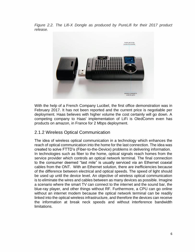
is light with a spectral range of 400 nm – 700 nm. The communications signal is overlaid on top of the illumination aspect of the – oftentimes white – light. The requirements for a VLC network would be multiple device configuration which is essentially a multi input multi output system. The network would be able to provide service to a laptop, TV, smart phone, wearable device, and comparable multimedia connections as opposed to a direct connection in which a LET may only be capable of. Harold Haas a German professor at the University of Edinburough in the Scottish capital first showcased in 2011 how light fidelity (LiFi) technology works with the media organization TED (technology, entertainment, design). The company he created out of his laboratory enterprise was PureLiFi. The system had a LED light which could be used in a regular high hat type implementation and had a USB compatible device as the receiver and uplink which was the relative size of a business card. The appearance of the device allows for the consumer to maintain the experience of integrated product. The way the LiFi system was presented was that the LED was modulated with a signal consisting of various light intensity variations. The optical signal was detected and converted into an electrical signal which was transferred to a computer instead of a multimedia device. The USB receiver had an infrared LED to provide full duplex bidirectional wireless access at the speed of 43 Mbps up and down respectively. The average rates of installation hovered around 25 Mbps and maintaining full duplex interaction. More specifically, the broadband white light can communicate simultaneously with multiple multimedia devices. If that specific multimedia devices changes white light sources, the system automatically adjusts in what is an adaptive algorithmic for the best connection. The LiFi-X Dongle as seen in Fig 3. is the fastest data transmission and current state of the art technology in the consumer marketplace (2017). Although we may not be able to directly replicate this type of device, the goal of the project was to get the group into the mode of understanding in undertaking such a product.
6
Figure 2.2. The Lifi-X Dongle as produced by PureLifi for their 2017 product release.
With the help of a French Company Lucibel, the first office demonstration was in February 2017. It has not been reported and the current price is negotiable per deployment. Haas believes with higher volume the cost certainly will go down. A competing company to Haas' implementation of LiFi is OledComm even has products on amazon, in France for 2 Mbps deployment.
2.1.2 Wireless Optical Communication
The idea of wireless optical communication in a technology which enhances the reach of optical communication into the home for the last connection. The idea was created to solve FTTD’s (Fiber-to-the-Device) problems in delivering information. In technologies such as fiber to the home, optical signals reach homes from the service provider which controls an optical network terminal. The final connection to the consumer deemed “last mile” is usually serviced via an Ethernet coaxial cables from the ONT. With an Ethernet solution, there are inefficiencies because of the difference between electrical and optical speeds. The speed of light should be used up until the device level. An objective of wireless optical communication is to eliminate the wires and cables between as many devices as possible. Imagine a scenario where the smart TV can connect to the internet and the sound bar, the blue-ray player, and other things without RF. Furthermore, a CPU can go online without an internet modem because the optical network terminal can be readily linked into the optical wireless infrastructure, and therefore the devices can receive the information at break neck speeds and without interference bandwidth limitations.
7
2.2 Objectives
2.2.1 Motivation
The group members decided to create a communications project and the medium chosen was light. This project should demonstrate how the group was able to focus on a problem such as wireless communication and cultivate a robust, efficient product from a reasonable approach and a thorough execution. The ability to work in a group and identify key ways to compliment strengths together, which are vital aspects of an engineering team, is introduced. By finding out how to go from an initial idea and follow through to make a product, present the material in question, and write a report the group will be addressing requirements set out to obtain an engineering degree from the University of Central Florida. Benjamin Stuart, is a photonic scientist and engineer who is actively engaged in communication research with fiber optics. He is looking to pursue a career in photonics with an emphasis on obtaining information from the natural world or in propagating information. He is also well versed in material characteristics for laser engraving and decapsulation. He is also interested in bio-photonics which is related directly to this project where the transmitting laser with a high frequency can create novel imaging techniques. He was having been assigned as the project manager, responsible for the overall robustness, and continuity of the design in each aspect and interfacing with each group member in order to establish their goals and responsibilities. Garrett Bennett, also a photonic scientist and engineer is looking to pursue a career in RF design of antennas and semiconductor design. He hopes to go to Master’s school for this specialty. He is actively working for TRS wireless, a radio and telephone communications company. Garrett was responsible for the prototype assembly and in making sure the optical system can handle the requirements. In addition, for the final design, he will construct the physical housing. George Salinas is a computer engineer, he is interested in the technology of wireless communications networks and the interfacing of the incoming and outgoing signal of internet technology. He aspires to work on technologies to increase the throughput of communication technology. George was given the responsibility of researching communications technologies that could be implemented with the given optical wireless communication system. Zhitao Chen is an electrical engineer. Zhitao is interested in electrical circuit design. Zhitao was in charge of designing the power supply to the VLC system, which included properly implementing the LED and photodiode. Zhitao was given a duty to test the power supply. Also, had responsibility for design of a PCB through KiCAD as well as manufacturing and ordering.

8
2.2.2 Goals
Our goal was to provide an easy to assemble and robust optical wireless transceiver. The internet transmission will be directed through a modulated light beam which can be in any part of the visible spectrum. The system will has a readily available information display which is software based to check the transmission information such as speed, bandwidth, error rates, IP address, and verifiable connection to the internet. The interface should allow for the user to understand the top-level application extracted information. The hardware was able to be impacted and be weather resistance. The device should be accurate, and efficient. The efficiency over the RF repeater should be apparent and the easily identifiable troubleshooting particulars. We tried to make the design as sleek and robust as possible to not make it intrusive and the final product should be more than capable of upgrades.
2.3 Requirements Specifications Unless a specific component is mentioned "The product" refers to our VLC design and its components and accessories as a whole.
The product shall be no larger than 5 cubic in.
The product shall weigh no more than 5 lbs.
The product shall contain an LED, a power supply, and an Ethernet port.
The product shall be able to transmit data at a rate of at least 5 Mbps.
The product shall not interfere with existing wireless communication infrastructure.
The user side of the product shall be compatible with any Ethernet equipped computer.
The user side of the product should be able to have a USB to Ethernet converter option.
The product can function as a repeater for Ethernet connection.
The connected information should be able to be free of errors to the defined amount in the standards.
The product shall be non-hazardous to the user.
There should be fail safe mechanical mechanisms.
Caution warnings for light illumination should be supplied.
Usable, intuitive, and easy to learn.
The product shall cost less than $300.
The product shall not use more than 45 V supply at a time.
The product will not use more than 1.5 A at a time.
2.4 Market and Engineering Requirements

9
The house of quality represents a visual overview of the system requirements. In order to obtain the above relationships our product should be well engineered and tested. The trouble shooting aspect is the root of where the practice of understanding our project.
Figure 2.3. The house of quality of the system specifications.
The two sides of the house of quality are the customer requirements and the engineering requirements. The items listed on the left are potential needs of the customer in order to be satisfied with the product. Here cost refers to the total price a customer would pay for a VLC system. In this scenario, the size of the receiver is referring to the size of the device that plugs into the user's PC. Although the VLC system uses two transceivers, the network switch side of the system is negligible in size. Overall things such as cost, size, and energy consumption all benefit the customer if they are lesser. The ease of installation and speed are a positive factor
10
where "more" is better. The VLC system makes use of existing internet infrastructure and is comparable to the price and speed of current internet-enabling devices. Across the top of the "house" are engineering requirements, that are meant to be taken into account when designing the system itself. There are duplicates from the customer requirements because they are key factors when designing the system. For instance, the cost of engineering refers to the amount of money to research, develop, and manufacture a finished product, the lower this number the better. The Tx Efficiency is an interesting requirement, because VLC makes use of existing infrastructure the system can only be as fast as it's connected counterparts. This means that the VLC system needed to be designed in a way that there was as little circuit parasitic as possible, and that all the components can operate well above the speed of any given infrastructure.
2.5 Distribution and Hierarchical Layout Even though senior design is a group work, we still needed to make sure each group member gained the most educational value from this project. Our team had a weekly meeting, however, when it is necessary, we do had a biweekly meeting. The different topics of this projects design and construction have been divided according to work load for each person and the respective interests of the team members. In order to establish the distribution of responsibilities to the project, the following layout in Fig. 2.4 is a hierarchical overview of the design of the project. The red indicates work done by the photonics team in Benjamin Stuart and Garrett Bennett, the blue was the responsibility of Zhitao Chen, and the green is the work done by George Salinas. The purple indicates the joint decisions by the electrical and photonics team. The basis of our project inherently combines the understanding of electronic systems on to optical considerations.

11
Figure 2.4 The project distribution and hierarchical layout.
2.5.1 Contribution Breakdown
For our project, the team can be broken down into three categories, we have the
optics, the electronics, and the software. Ben and Garrett, as part of the optics
team were tasked with the optics portion of the project including opto-electronics.
Responsibilities include selecting all optical components including but not limited
to the photo-diode, the laser diode or LED, the focusing elements such as lenses,
and the implementation encompassed by all the aforementioned components. In
addition, the optics team was heavily involved in selecting the electronics used to
control the optical devices where needed, as well as the overall design/layout of
the system. On the electronics portion of the team is Zhitao, he was tasked with
the design and implementation of all power components including power supplies
and amplifiers as well as fundamental electronic components. In addition, Zhitao
was tasked with the design of the PCB for the system. On the software team is
Jorge, he was tasked with the generation of a signal representing a standard
internet connection, as well as the recovery of said signal. In addition, Jorge was
tasked with writing software to capture and analyze data going through the VLC
system.
2.6 Design Comparison When investigating the theory and operation of transmitting information over light, the group determined two separate types of transmission – light communication with lasers or with white light emitting diodes or LEDs.

12
The process of developing a transceiver for both prototypes was pursued and documented for the white LED in chapter 5. The prototype construction was attempted in chapter 7 was for the 10 Base-T LED construction while chapter 8 will focus more on how to create the PCB for a laser diode optical transceiver. The group was unable to successfully demonstrate either the 10 Base-T or the 100 Base-T for the white LED system, however, after further review we have concluded in demonstrating a workable transceiver system based upon laser light transmission. Although the laser system will not be able to light up a room, or looked at directly, it is a powerful tool in situations where laying a physical cable is not feasible such as underwater communication, or rough terrain. The team made great strides in understanding of communication systems in light and Ethernet protocols and feels this project has helped in creating that understanding.
13
3. Research related to Project
There are only two ways which can be used in photonic information transmission, that is free space or fiber optics. The differences in each medium gives rise to different problems such as transmission wavelength, absorption, and scattering loss. The ideal situation is where there is no absorption or scattering at a given transmission window. Although photons intrinsically are immune to electromagnetic radiation in the radio-frequency domain, i.e. they are less prone to decohere or lose their phase or polarization, the absorption and scattering causes power loss, and decreases the signal to noise ratio. Absorption loss is primarily the default in fiber optics in that the material such as silica absorbs the light, whereas, free space communication has difficulties in turbulence and scattering such as Mie scattering. Our project will utilize optical free space communication and therefore it is paramount to understand the proper adjustments.
3.1 Relevant Technologies This section will cover the various technologies we considered for our projects, including different applications within separate subsystems. The direct implementation will be presented with the relevant basic understanding required for the physics to engineering execution.
3.1.1 Transmitter Technology
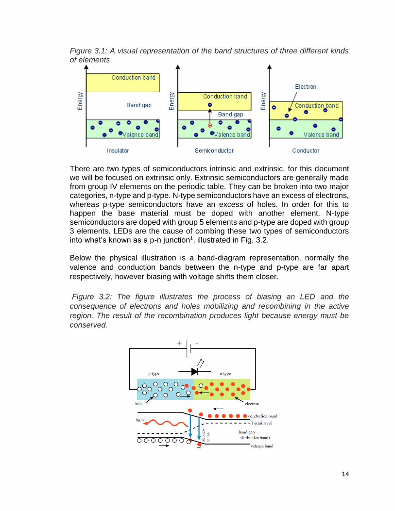
LED LEDs or Light emitting diodes are a solid-state technology that convert electrical signals into light waves. Starting with the basics, a diode is the simplest form of a semiconductor. The semiconductor can act as either a conductor or an insulator. When considering materials that allow or deny the flow of electrons the concept of energy bands comes into play. For conductors, the valance band and the conduction band of an element or material touch each other, for an insulator these two bands are far apart, for a semiconductor they are somewhere in the middle. Fig. 3.1 shows this concept.
14
Figure 3.1: A visual representation of the band structures of three different kinds of elements
There are two types of semiconductors intrinsic and extrinsic, for this document we will be focused on extrinsic only. Extrinsic semiconductors are generally made from group IV elements on the periodic table. They can be broken into two major categories, n-type and p-type. N-type semiconductors have an excess of electrons, whereas p-type semiconductors have an excess of holes. In order for this to happen the base material must be doped with another element. N-type semiconductors are doped with group 5 elements and p-type are doped with group 3 elements. LEDs are the cause of combing these two types of semiconductors into what’s known as a p-n junction1, illustrated in Fig. 3.2. Below the physical illustration is a band-diagram representation, normally the
valence and conduction bands between the n-type and p-type are far apart
respectively, however biasing with voltage shifts them closer.
Figure 3.2: The figure illustrates the process of biasing an LED and the
consequence of electrons and holes mobilizing and recombining in the active
region. The result of the recombination produces light because energy must be
conserved.

15
When voltage is applied to the LED electrons from the n side move towards the p side and holes from the p side move toward the n side. In the center is a recombination region where the holes and electrons combine into single pairs commonly referred to as EHPs or electron-hole pairs. Since there is an energy difference between the electrons and holes when they recombine there is an energy dissipation in the form of light and heat. In order for this process to occur the junction must be forward biased, the required voltage bias is a function of the materials and changes according to substrate, dopants, acceptors, etc. LEDs generally only require a few volts to operate. The color of emitted light is also directly proportional to the bandgap of the p-n junction represented by the equation
𝐸𝑔 =ℎ𝑐
𝜆 , where “hc” is Planck’s constant multiplied by the speed of light, lambda
is the wavelength of emitted photons, and Eg is the bandgap of the LED. For the VLC project we are using a broadband LED, it emits multiple wavelengths and gives the appearance of white light. Laser Types In addition, there are several types of lasers which fundamentally differ in structure and functionality in a design because of their package layout, optical configurability (wavelength tunability), chemical composition, and mechanical construction. The different types of semiconductor lasers include but are not limited to:
Fabry-Perot Diode Lasers
Heterostructure Diode Lasers
Distributed Feedback Lasers
Quantum Cascade Lasers (QCL)
Vertical Cavity Surface Emitting Laser (VCSEL) Fabry-Perot Diode lasers are pumped from a semiconductor laser into a resonator cavity. The resonator cavity creates longitudinal modes with a wide spectral selection than may be necessary, therefore it is not a good candidate. Heterostructure diode lasers have coherent output, easy to work with packaging and small spectral width. Distributed feedback lasers utilize a diffraction grating in the semiconductor material to eliminate wavelength dispersion and create a small spectral width, however their packaging is not as easy to utilize in our design. Again, although the characteristics of VCSEL, and QCL are appealing in high power conversion efficiency, spectral selection, and discrete packaging, their overall form factor requires more understanding to incorporate into our design. Given our time constraints and monetary budget, our choice will be heterostructure diode lasers. Some other types of lasers which exist:
Gas Lasers
Excimer Lasers
Solid State Lasers
16
Gas Lasers use a gas as a gain material for population inversion. When a current is sent through the electrodes of the cathode and anode the energy from the electrons create an excitation in the gas atoms from electron collisions, thus creating a population inversion. Excimer lasers are photolithographic lasers which operate in the EUV spectrum to engrave integrated microchips in semiconductor manufacturing. Solid state lasers are created by optically pumping a crystal which acts as a gain medium for then transforming the incoming light into a different wavelength based on the transmission spectrum. The later types of lasers are out of the scope of this project because their properties require complex mechanical construction.
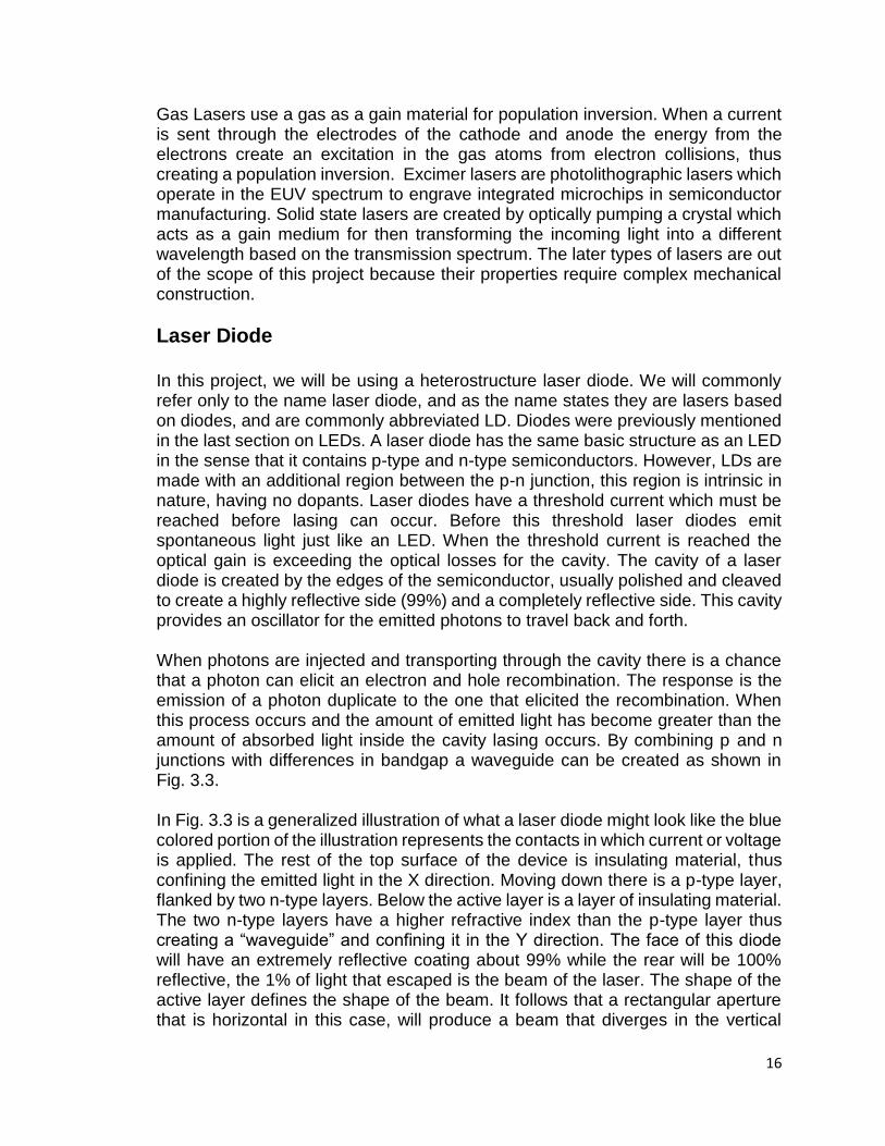
Laser Diode In this project, we will be using a heterostructure laser diode. We will commonly refer only to the name laser diode, and as the name states they are lasers based on diodes, and are commonly abbreviated LD. Diodes were previously mentioned in the last section on LEDs. A laser diode has the same basic structure as an LED in the sense that it contains p-type and n-type semiconductors. However, LDs are made with an additional region between the p-n junction, this region is intrinsic in nature, having no dopants. Laser diodes have a threshold current which must be reached before lasing can occur. Before this threshold laser diodes emit spontaneous light just like an LED. When the threshold current is reached the optical gain is exceeding the optical losses for the cavity. The cavity of a laser diode is created by the edges of the semiconductor, usually polished and cleaved to create a highly reflective side (99%) and a completely reflective side. This cavity provides an oscillator for the emitted photons to travel back and forth. When photons are injected and transporting through the cavity there is a chance that a photon can elicit an electron and hole recombination. The response is the emission of a photon duplicate to the one that elicited the recombination. When this process occurs and the amount of emitted light has become greater than the amount of absorbed light inside the cavity lasing occurs. By combining p and n junctions with differences in bandgap a waveguide can be created as shown in Fig. 3.3. In Fig. 3.3 is a generalized illustration of what a laser diode might look like the blue colored portion of the illustration represents the contacts in which current or voltage is applied. The rest of the top surface of the device is insulating material, thus confining the emitted light in the X direction. Moving down there is a p-type layer, flanked by two n-type layers. Below the active layer is a layer of insulating material. The two n-type layers have a higher refractive index than the p-type layer thus creating a “waveguide” and confining it in the Y direction. The face of this diode will have an extremely reflective coating about 99% while the rear will be 100% reflective, the 1% of light that escaped is the beam of the laser. The shape of the active layer defines the shape of the beam. It follows that a rectangular aperture that is horizontal in this case, will produce a beam that diverges in the vertical

17
direction, and vice versa. It also follows that the smaller the aperture the larger the divergence rate.
Figure 3.3 A generalized illustration of what a laser diode might look like.
Naturally, all transmitters have a divergence however the reason why lasers for RF communication have been so highly pursued in military situations is the lack of divergence angle. The small change in divergence allows for the chance of interception to be minimal and reception to be relatively line of sight, the drawback is the cost of transmission distance in terms of power efficacy. The reason why lasers have a small divergence angle is because of interrelating aspect of the waist and the divergence. In Gaussian beams, the waist of the beam is point of least diameter as seen from the axial point of view, also referred to as the propagation direction. The waist of the beam and the divergence angle are proportional when one increases, as does the other.
Figure 3.4. A diagram showing a laser diode being used as a transmitter, its beam diverges by and angle θ over the length L, a lens is placed at that length to intercept the beam and focus onto a receiver.

18
Furthermore, laser diodes have power to current graphs which explain the threshold characteristics. The laser diode will only produce significant optical power when driven above the threshold current. The threshold current is referred to as the required bias current as seen in Fig 3.5. Below threshold, the photons are produced by spontaneous emission and have a larger spread of energies the device operates in the LED mode. Above threshold, only the photons with energies that experience the largest gain will become lasing photons and therefore the spectrum is narrow, and the devices operates as a laser diode. In addition, thermal dependencies of temperature effect power to current output whereas with an increased temperature, the current required for the same power is higher. Usually a linear approximation can be made within the small temperature range however since our system is inherently analog experimental data should be established to where this cut off temperature is. The reason why this is useful is because the output optical power can essentially slave the input current to the device to match the modulation signal.
Figure 3.5. The optical power to current graph, displaying the bias current point and the threshold current dependence on temperature.
Ethernet Ethernet technology was invented in the late 1970s and has been a crucial part of networking ever since. It was developed as a local area network technology meant to allow any devices connected by Ethernet to communicate with one another. It works on the Physical layer as well as the Data Link layer. Originally Ethernet made use of single coaxial cables, and then developed into twisted pair cable, and

19
nowadays fiber optic cables. The most common medium for Ethernet is twisted pair cables that can be classified as category 3, 5, 5e, 6, 6a and most recently 8.1/8.2. In 1980 IEEE decided to standardize Ethernet technology under the group 802.3 as it was becoming so wide-spread. In 1990 Ethernet moved to a twisted pair cabled medium under the name 10BASE-T. 10BASE-T networks have a speed of 10 Mbit/s and are ran on category 3 cabling. Several years later came “Fast Ethernet” under the name of 100BASE-T, these networks were rated at speeds of 100 Mbit/s and required at least category 5 cabling. A few years after that came 1000BASE-T which has a network speed of 1000 Mbit/s and requires category 5e or category 6 cabling. More information is provided in the next section. Most Ethernet connection use an 8P8C port as shown in Fig. 3.6. This type of port is found across millions of devices and enables them to communicate on local area networks just by simply plugging them in. The impact of Ethernet is still relevant today as new standards are still being implemented some 40+ years later.2
Figure 3.6: An 8P8C connector, meaning eight positions eight contacts is an almost universal connector for Ethernet devices. It is crimped onto the end of a twisted pair cable (which contain 4 pairs) and each wire takes a single position on the face of the connector.
Twisted Pair Cables Twisted pair cables have been the medium of choice for local area networks for the past 30 years. Fig. 3.7 shows a comparison between the different unshielded twisted pair (UTP) categories. The reason the pairs are twisted is together is to remove electromagnetic interference. In practice, the number of twists per meter is something that aids in how much capacity the cable can carry. In the table in Fig 3.7, we can see the cable category, its application, and its data rate. One parameter missing is the bandwidth measured in MHz. The required bandwidth is a function of the desired speed and symbol value of the data. The symbol value
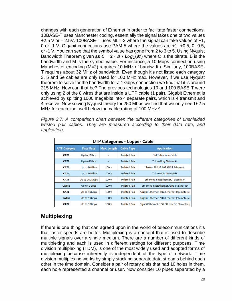
20
changes with each generation of Ethernet in order to facilitate faster connections. 10BASE-T uses Manchester coding, essentially the signal takes one of two values +2.5 V or – 2.5V. 100BASE-T uses MLT-3 where the signal can take values of +1, 0 or -1 V. Gigabit connections use PAM-5 where the values are +1, +0.5, 0 -0.5, or -1 V. You can see that the symbol value has gone from 2 to 3 to 5. Using Nyquist Bandwidth Theorem given as 𝑪 = 𝟐 ∗ 𝑩 ∗ 𝑳𝒐𝒈𝟐(𝑴) where C is the bitrate, B is the bandwidth and M is the symbol value. For instance, a 10 Mbps connection using Manchester encoding (M=2) requires 10 MHz of bandwidth. Similarly, 100BASE-T requires about 32 MHz of bandwidth. Even though it’s not listed each category 3, 5 and 5e cables are only rated for 100 MHz max. However, if we use Nyquist theorem to solve for the bandwidth for a 1 Gbps connection we find that it is around 215 MHz. How can that be? The previous technologies 10 and 100 BASE-T were only using 2 of the 8 wires that are inside a UTP cable (1 pair). Gigabit Ethernet is achieved by splitting 1000 megabits into 4 separate pairs, which is 4 transmit and 4 receive. Now solving Nyquist theory for 250 Mbps we find that we only need 62.5 MHz for each line, well below the cable rating of 100 MHz.2 Figure 3.7. A comparison chart between the different categories of unshielded twisted pair cables. They are measured according to their data rate, and application.
Multiplexing If there is one thing that can agreed upon in the world of telecommunications it’s that faster speeds are better. Multiplexing is a concept that is used to describe multiple signals over a single medium. There are a number of different kinds of multiplexing and each is used in different settings for different purposes. Time division multiplexing (TDM), is one of the most widely used and adopted forms of multiplexing because inherently is independent of the type of network. Time division multiplexing works by simply stacking separate data streams behind each other in the time domain. Consider a pair of rotary dials that had 10 holes in them, each hole represented a channel or user. Now consider 10 pipes separated by a

21
stream connected by the dials, and that were each sending 1 unit of data at a rate 10x slower than the speed of the rotary dial. For every one revolution of the rotary dial each pipe would send 1 unit of data into the stream. On the receiving end, the opposite occurs where another rotary dial is synced with the first one to transfer the data across the stream from pipe 1 to pipe 1, pipe 2 to pipe 2 and so on and so forth. In practice, the speed at which this occurs is unperceivable to the users (in this example the pipes). Fig. 3.8 represents this concept.
Figure 3.8. A graphical representation of TDM, you can see the signals one after another, the loop network makes sure the first channel exits into the first channel and so on.
Another form of multiplexing that is commonly used is frequency division multiplexing (FDM). Frequency division is one of the most common forms of multiplexing in analog systems. This is especially apparent in systems of AM and FM radio, and television broadcasts. Frequency division in principle works just how the name says, a certain band of frequencies are allocated to each channel. Fig. 3.8 shows this concept. For a real-life example, you can look at FM radio stations, the spectrum starts at about 88 MHz and ends at about 108 MHz. When you change the dial on your radio (tune it) you see that the stations are separated by 200 KHz channels. This method allows multiple signals to be broadcast simultaneously through the same medium (air). In optical fibers FDM is just considered as using different colors for different channels which is also referred to as wave division multiplexing. Since the signal carrier is in the THz region in fiber optics, when FDM is employed the channel bandwidths are extremely large. Some VLC systems use this technique by implementing a multicolored LED. To elaborate a regular white light LED is usually really a single diode that is blue and the color is transformed when it is mixed with yellow phosphor giving a white appearance. However, there are white light LEDs like those in your television that combine three colors red, blue, and green to form a white light source. When implemented into a VLC system each light can be modulated individually thus produces a 3-channel multiplexed system given the area of reception has appropriate filtering.
22
Figure 3.9. A graphical representation of FDM, this shows three 20 KHz channels occupying about 60 KHz of total bandwidth.
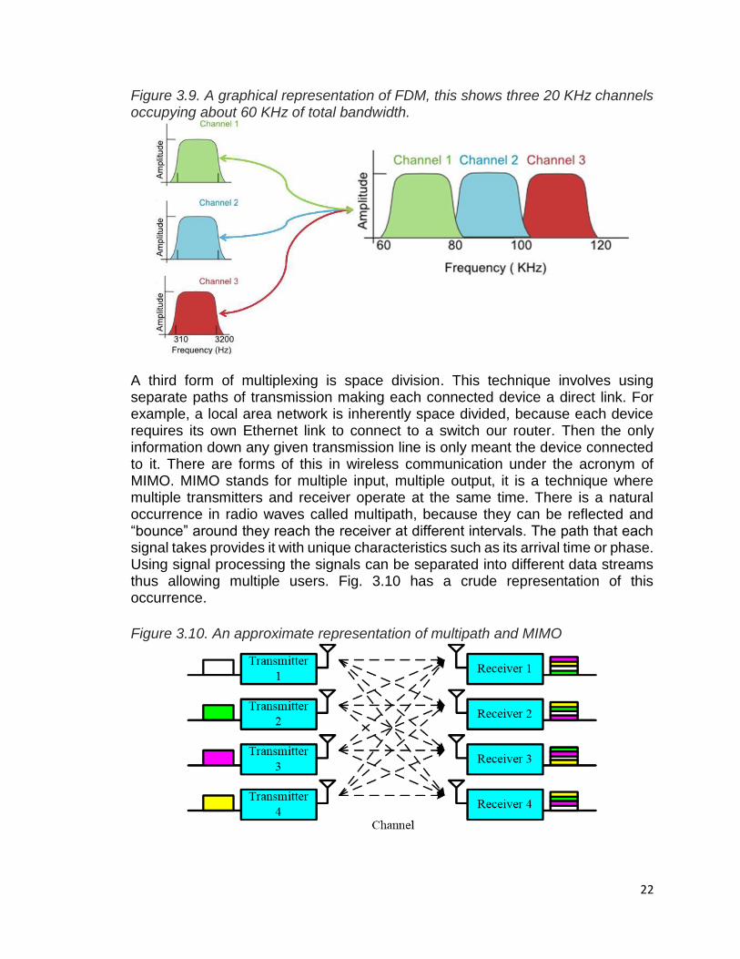
A third form of multiplexing is space division. This technique involves using separate paths of transmission making each connected device a direct link. For example, a local area network is inherently space divided, because each device requires its own Ethernet link to connect to a switch our router. Then the only information down any given transmission line is only meant the device connected to it. There are forms of this in wireless communication under the acronym of MIMO. MIMO stands for multiple input, multiple output, it is a technique where multiple transmitters and receiver operate at the same time. There is a natural occurrence in radio waves called multipath, because they can be reflected and “bounce” around they reach the receiver at different intervals. The path that each signal takes provides it with unique characteristics such as its arrival time or phase. Using signal processing the signals can be separated into different data streams thus allowing multiple users. Fig. 3.10 has a crude representation of this occurrence.
Figure 3.10. An approximate representation of multipath and MIMO

23
3.1.2 Receiver Technology
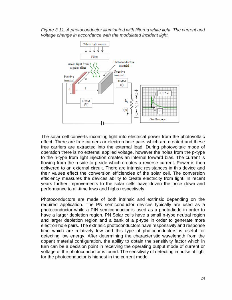
Photodevices The 'heart' of a photodevice converts light into electric current because of the properties of semiconductors. Photodiodes illuminated by light and without external bias can generate electric current, and we refer to this mode of operation as photovoltaic. The photoconductive mode is characterized by an external bias. When an external bias voltage is applied, photodiodes conduct current and the current to voltage graphs have a linear regime. When light is absent, only a smaller 'dark' current can flow under reversed bias. When under illumination, photons absorbed in the semiconductor create electrons and holes that can essentially move from the electric field across the photodiode. The amount of electron and hole pairs created and thus maximal electric current is proportional to light intensity. There are several significant receiving devices for light, however their uses have applications which their functions are interrelated. The various names for receiving devices are PN junction, phototransistor, photovoltaic and solar cell, which are the same concept, a PIN photodiode characterized by its thin and discrete P-type outer layer for maximal photon penetration and electron generation, and finally a photoconductor. The photoconductive effect takes place when there is incident light on a photoresistor, or photoconductor. The photons are absorbed in the semiconductor and create free carriers that conduct electric current across the diode. The quantity of free carriers created and the electric current is proportional to light intensity given by IL = KP where K is the responsivity of the device. This is the meaning of photoconductive mode. In low light energy situations and monochromatic wavelengths, the conductance is a useful tool in measuring the optical power without a power meter however for our purposes the response time limits the applications of communication. In Fig 3.11, incident light is on a photoresistor and the resulting output is seen with a time constant delay according to the resistor and capacitance of the device. In a photoconductor, the photo-absorption is proportional to the density of the impurity material which determines the penetration of light distance into the material and an extrinsic semiconductor with less minority carriers would have a slower charge recombination time. The transit time of this slow carrier represents the duration of this photoconductive process and affects the bandwidth of photoconductive detectors. Therefore, the fundamental limit of the bandwidth is the minority carrier recombination lifetime. The photoconductor or a photoresistor has a resistance proportional the incoming optical power which is the photoconductive effect.
24
Figure 3.11. A photoconductor illuminated with filtered white light. The current and voltage change in accordance with the modulated incident light.
The solar cell converts incoming light into electrical power from the photovoltaic effect. There are free carriers or electron hole pairs which are created and these free carriers are extracted into the external load. During photovoltaic mode of operation there is no external applied voltage, however the holes from the p-type to the n-type from light injection creates an internal forward bias. The current is flowing from the n-side to p-side which creates a reverse current. Power is then delivered to an external circuit. There are intrinsic resistances in this device and their values effect the conversion efficiencies of the solar cell. The conversion efficiency measures the devices ability to create electricity from light. In recent years further improvements to the solar cells have driven the price down and performance to all-time lows and highs respectively. Photoconductors are made of both intrinsic and extrinsic depending on the required application. The PN semiconductor devices typically are used as a photoconductor while a PIN semiconductor is used as a photodiode in order to have a larger depletion region. PN Solar cells have a small n-type neutral region and larger depletion region and a bank of a p-type in order to generate more electron hole pairs. The extrinsic photoconductors have responsivity and response time which are relatively low and this type of photoconductors is useful for detecting low energy. After determining the characteristic wavelength from the dopant material configuration, the ability to obtain the sensitivity factor which in turn can be a decision point in receiving the operating output mode of current or voltage of the photoconductor is found. The sensitivity of detecting impulse of light for the photoconductor is highest in the current mode.
25
For a photodiode in the photoconductive mode of operation the semiconductor is reverse biased and power is delivered to the photodiode. For the PIN photodiode, the large reverse bias increases the depletion region and area of detection, which in turn decreases the transit time and the capacitance of that region. The decreased transit time and capacitance allows for the device to operate at larger frequencies.3
Figure 3.11. The PIN Photodiode diagram in reverse bias illustrating how a photon can induce free carrier (electrons and holes) transport.
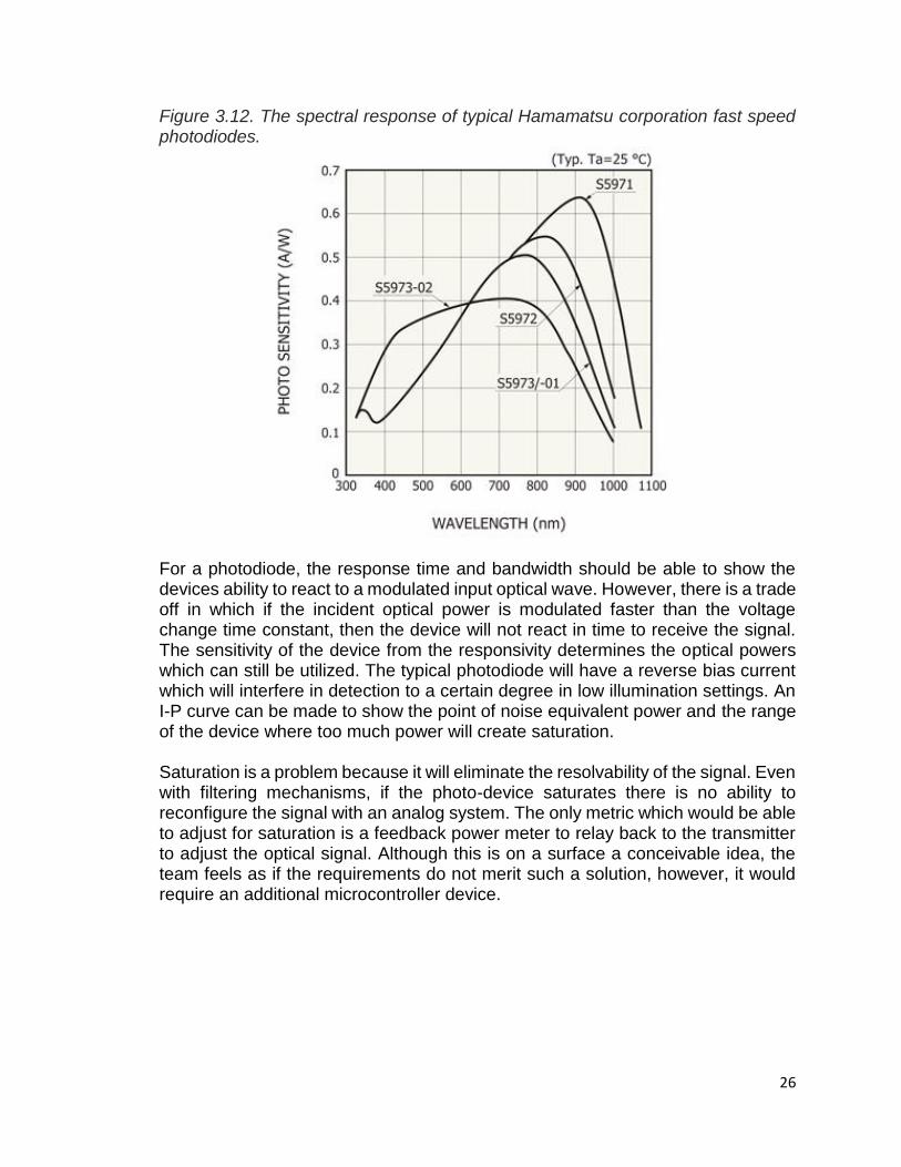
The spectral response of the device is a critical point of reference for every photodiode because it shows the range of the applicable responsivity. Depending on the dopant material which controls the bandgap and thus acceptable energy photon which can induce free carrier transport, each photodiode device has a particular range. The Fig 3.12 shows the typical spectral response characteristics seen from a photodiode manufacturer, and the goal of the group is to find a device which is specific to the lighting device which we are using. Therefore if both devices are suitable for each other we should get the best response out of the photodiode.
26
Figure 3.12. The spectral response of typical Hamamatsu corporation fast speed photodiodes.
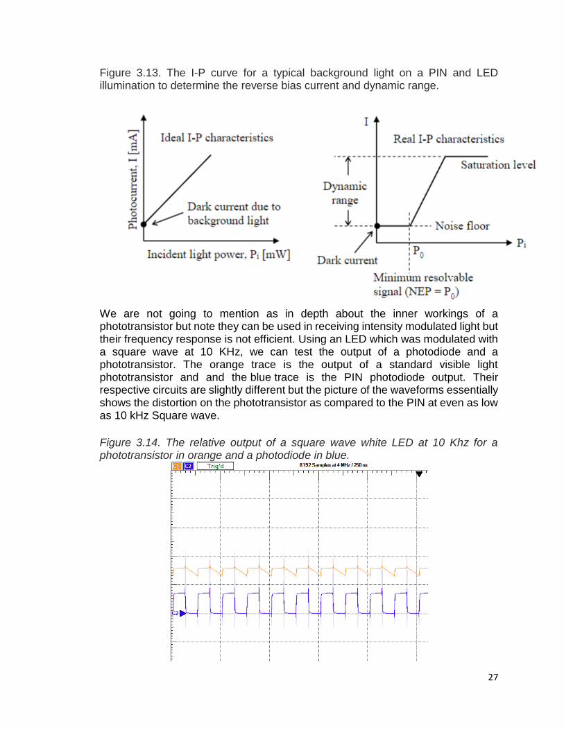
For a photodiode, the response time and bandwidth should be able to show the devices ability to react to a modulated input optical wave. However, there is a trade off in which if the incident optical power is modulated faster than the voltage change time constant, then the device will not react in time to receive the signal. The sensitivity of the device from the responsivity determines the optical powers which can still be utilized. The typical photodiode will have a reverse bias current which will interfere in detection to a certain degree in low illumination settings. An I-P curve can be made to show the point of noise equivalent power and the range of the device where too much power will create saturation. Saturation is a problem because it will eliminate the resolvability of the signal. Even with filtering mechanisms, if the photo-device saturates there is no ability to reconfigure the signal with an analog system. The only metric which would be able to adjust for saturation is a feedback power meter to relay back to the transmitter to adjust the optical signal. Although this is on a surface a conceivable idea, the team feels as if the requirements do not merit such a solution, however, it would require an additional microcontroller device.
27
Figure 3.13. The I-P curve for a typical background light on a PIN and LED illumination to determine the reverse bias current and dynamic range.
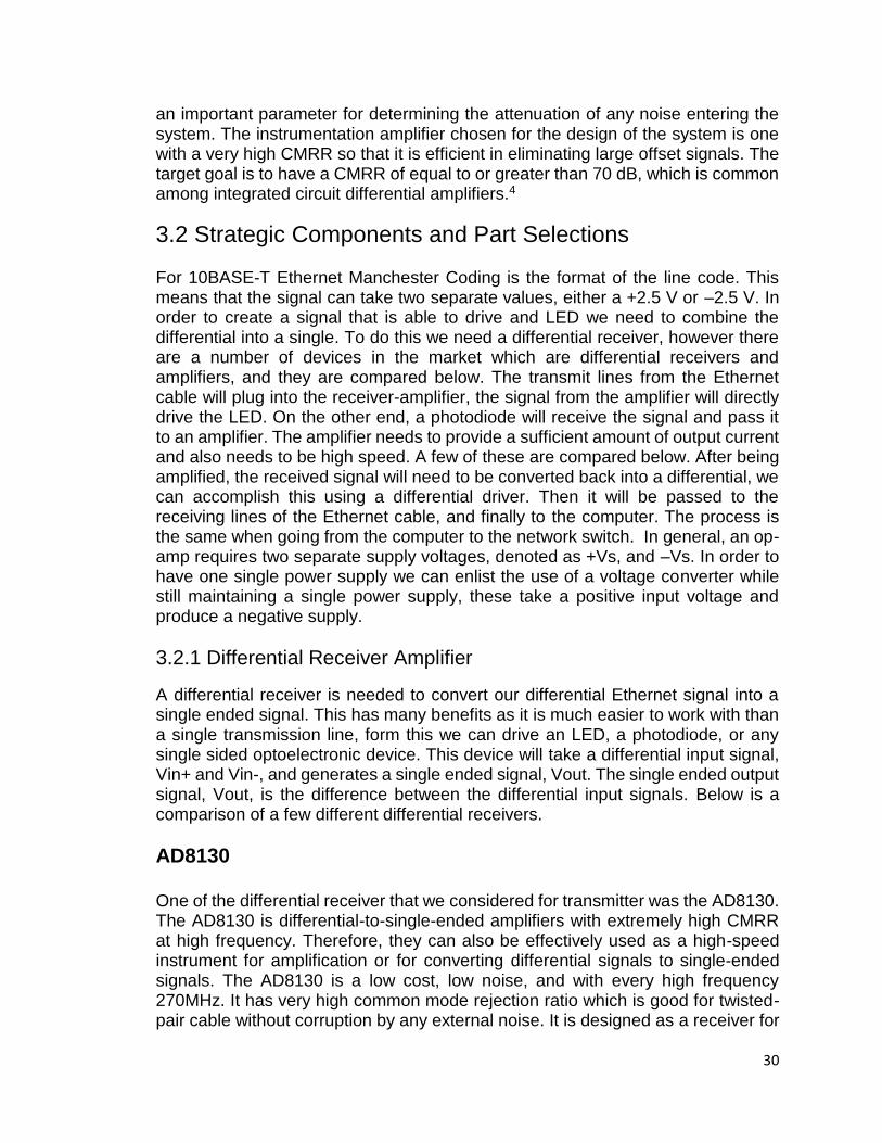
We are not going to mention as in depth about the inner workings of a phototransistor but note they can be used in receiving intensity modulated light but their frequency response is not efficient. Using an LED which was modulated with a square wave at 10 KHz, we can test the output of a photodiode and a phototransistor. The orange trace is the output of a standard visible light phototransistor and and the blue trace is the PIN photodiode output. Their respective circuits are slightly different but the picture of the waveforms essentially shows the distortion on the phototransistor as compared to the PIN at even as low as 10 kHz Square wave.
Figure 3.14. The relative output of a square wave white LED at 10 Khz for a phototransistor in orange and a photodiode in blue.

28
Photodiodes can be used in a wide range of applications however their structural material changes depending on the region of the spectrum. Therefore, depending on the application the detector can be chosen to match the power levels, spectrum, and speed.
3.1.3 Detection Statistics
In order to explain more about how error detection occurs, a little background on photon statistics is necessary. The statistical distribution of the number of photons depends on the nature of the light source. For coherent light with constant optical
power P, the corresponding mean photon flux Φ =𝑃
ℎ𝜈 (photons/s) is also constant,
but the actual times of registration of the photons are random. If the number of
photons detected in a time T is n, then the mean value of n is �̅� = Φ𝑇 = 𝑃𝑇
ℎ𝜈. The
probability distribution 𝑝(𝑛 ), i.e., the probability 𝑝(0), of detecting no photons, the probability 𝑝(1), of detecting one photon, and so on, may be measured by experimental observation. However due to the tedious nature of the required equipment and the practicality of a product, a Poisson distribution approach can be used. If the registration of photons are statistically independent, the Poisson
distribution is obtained: 𝑝(𝑛) =�̅�𝑛 exp(−�̅�)
𝑛! where n = 0,1,2,3,4… photons for �̅� mean
number of photons. The uncertainty 𝜎𝑛 = √�̅�, which the presence of �̅� photons is
accompanied by an inaccuracy of ± 𝜎𝑛 photons.1
Table 1: The photon detection choices.
Detection No Detection
Photon presence Signal Recorded - 1
Missed signal error, BER
No Photon Presence
Dark current, noise in system
Signal absent - 0
The probability of error, or bit error rate (BER) at 0 photons with high power is 𝑝𝑒 =exp(�̅�). The design of any instrument for sensing must take into account the signal to noise ratio because the detector can produce a response without light. The typical value required for a reasonable system is at least 10-6 for the BER. The noise which is introduced into the system should be identified. The noise includes four different types in readout noise, shot noise, dark noise, and fixed pattern noise. The readout noise is from the electrical circuit such as wires and insertion loss. The shot noise is the variation in the current due to photon flux. The dark noise is the variation in electrons generated without an incident light which passes through the system created by recombination. Fixed pattern noise is a variation is a in the photo-response due to the physical interface of the detection area. The noises can be accounted for in the signal to noise ratio.

29
3.1.4 Electrical Processing
Operational Amplifiers
Since we are working on the transmitter data, we need an op-amp to be high slew rate and also high speed. Slew rate is the change of voltage per unit of time. Slew rate and bandwidth tend to be linked - high speed op-amps tend to have fast slew rates, otherwise there will be a mismatch in data in to possible data out.
The Hamamatsu recommended high speed photodetector circuit is in Fig. 3.17. The PD is PIN photodiode, RL, R, Rf are values for specific operational amplifier gain calculations. Where 𝐼𝑠𝑐 is equivalent to the electrical analysis of the diagram.
𝑉𝑜 = 𝐼𝑠𝑐(1 +𝑅𝐹
𝑅𝐿)
Figure 3.15. The high-speed photodiode circuit (Courtesy of Hamamatsu).
Differential amplifiers Differential amplifier is the amplifier that amplifies the difference between two inputs. The output is Vout=AV(VIN
+-VIN-). In the transmitter side, we are using the
single ended output that combines the signal which comes from the Ethernet. In the receiver side, we are using the single ended input that convert back to a differential output.
Common Mode Rejection Ratio The common mode rejection ratio (CMRR) is a number that describes how well an input or output will reject noise or how well "balanced" a balanced line is. It is relatively easy to calculate CMRR. CMRR is measured in decibels (dB) of the differential mode gain and the common mode gain. In terms of signal fidelity, it is
30
an important parameter for determining the attenuation of any noise entering the system. The instrumentation amplifier chosen for the design of the system is one with a very high CMRR so that it is efficient in eliminating large offset signals. The target goal is to have a CMRR of equal to or greater than 70 dB, which is common among integrated circuit differential amplifiers.4
3.2 Strategic Components and Part Selections For 10BASE-T Ethernet Manchester Coding is the format of the line code. This means that the signal can take two separate values, either a +2.5 V or –2.5 V. In order to create a signal that is able to drive and LED we need to combine the differential into a single. To do this we need a differential receiver, however there are a number of devices in the market which are differential receivers and amplifiers, and they are compared below. The transmit lines from the Ethernet cable will plug into the receiver-amplifier, the signal from the amplifier will directly drive the LED. On the other end, a photodiode will receive the signal and pass it to an amplifier. The amplifier needs to provide a sufficient amount of output current and also needs to be high speed. A few of these are compared below. After being amplified, the received signal will need to be converted back into a differential, we can accomplish this using a differential driver. Then it will be passed to the receiving lines of the Ethernet cable, and finally to the computer. The process is the same when going from the computer to the network switch. In general, an op-amp requires two separate supply voltages, denoted as +Vs, and –Vs. In order to have one single power supply we can enlist the use of a voltage converter while still maintaining a single power supply, these take a positive input voltage and produce a negative supply.
3.2.1 Differential Receiver Amplifier
A differential receiver is needed to convert our differential Ethernet signal into a single ended signal. This has many benefits as it is much easier to work with than a single transmission line, form this we can drive an LED, a photodiode, or any single sided optoelectronic device. This device will take a differential input signal, Vin+ and Vin-, and generates a single ended signal, Vout. The single ended output signal, Vout, is the difference between the differential input signals. Below is a comparison of a few different differential receivers.
AD8130 One of the differential receiver that we considered for transmitter was the AD8130. The AD8130 is differential-to-single-ended amplifiers with extremely high CMRR at high frequency. Therefore, they can also be effectively used as a high-speed instrument for amplification or for converting differential signals to single-ended signals. The AD8130 is a low cost, low noise, and with every high frequency 270MHz. It has very high common mode rejection ratio which is good for twisted- pair cable without corruption by any external noise. It is designed as a receiver for
31
the transmitter for high speed signals over twisted-pair cables. AD8130 has a very high slew rate (1090 V/μs) which allows for the signal to be represented correctly. The device however has a high input impedance. The AD8130 can be supplied by a wide power supply range from single +5 V to ±12 V, allowing wide common mode and differential-mode voltage ranges while maintaining signal integrity. The gain of the device is based on the feedback resistors. The gain equation is the same as that of a conventional op-amp: 𝐺 = 1 + 𝑅𝐹/𝑅𝐺. The pin configuration used while testing unity gain in fig 3.18. For unity-gain applications using the AD8130, 𝑅𝐹 can be set to 0 and be seen as a short on the circuit.
Figure 3.16. The unity gain circuit for an AD 8129/30
In this design, our goal is to take a differential Ethernet signal into a single ended signal while maintaining low power. Also, we want it to be in the high frequency and high slew rate. AD8130 meets our requirements but also AD8130 already has three amplifiers internally which take care of the impedance. It already has three ICs built in which can also convert a differential line to a single ended line. This single-line signal is then transmitted out however it still has a high impedance required of 1 MΩ. Table 2. Pin configuration used whole testing the circuit
Pin Name Description
1 +IN Noninverting input
2 -VS Negative supply voltage
3 PD Input impedance
4 REF Positive Output.
5 FB feedback
6 OUT output
7 +VS Positive supply voltage
8 -IN Inverting input

32
MAX4444 Another option for the differential receiver that we considered for transmitter was the MAX4444. MAX4444 is differential-to-single-ended line receivers which offers high-speed and low-distortion performance. It is using a three-op-amp instrumentation amplifier architecture, and this IC has symmetrical differential inputs and a single-ended output. MAX4444 has extremely high slew rate. It operates at a frequency of 550MHz. It has 120mA output capability which allows the device to be directly coupled to a data acquisition system. It is suited to drive a coaxial cable. The high output current capability can easily drive the resistor impedance of common coaxial cables. It has s 55dB common mode rejection ratio, which is kind of a poor noise rejection criteria compared to other devices. The power supply range are from -5V-5V which is good for our design. The gain of a MAX4444 has an intrinsic RF in the gain equation making it harder to work with and may not produce any unity gain. The problem with this device is the output current is not sufficient for illumination.
THS4503 Another differential amplifier which has been considered is the THS4503. The THS4503 is from Texas Instruments. The THS4503 is high-performance fully differential amplifier. It is used for differential to single ended conversion. One good thing about this THS4503 is that the common mode rejection ratio is high. It has very good noise rejection criteria. Another advantage of the THS4503 is the power supply. It has a wide power supply range, and the power supply range is from -5V to 15V. However, the high frequency is not necessary although it has an excellent slew rate and it is kind of expensive compared to the other ICs.
EL4430 The EL4430 is an instrumentation amplifier which is ideal for differential to single ended converters. It has two sets of inputs; one which is connected to the signal and does not respond to its common-mode level, and another which is used to complete a feedback loop with the output. It can be operated on 5 and 15 supplies with no AC degradation. EL4430 has an excellent common mode rejection ratio. It is 70 dB which is very good noise rejection. The power supply range are from -5v to +5v. The EL4430 is stable for a gain of 1.
MAX4390 and MAX4392 MAX4390 and MAX4392 are dual-supply, rail-to-rail, voltage-feedback amplifiers that employ current-feedback techniques to achieve 500V/μs. This family of devices are a unity-gain device capable of 85 Mhz output. It also has rail-to-rail output which essentially allows both input sides to have an input and output voltage swing which stay linear. The device only consumes 5.5mA of current in order to be
33
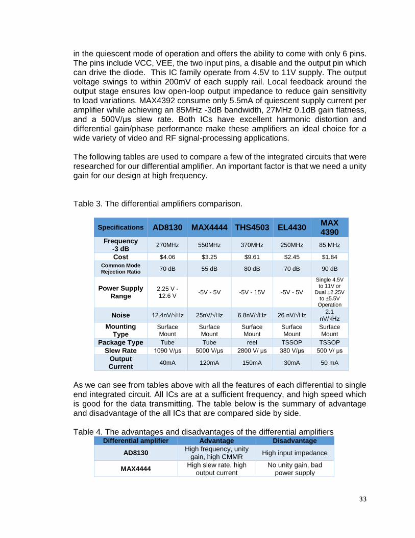
in the quiescent mode of operation and offers the ability to come with only 6 pins. The pins include VCC, VEE, the two input pins, a disable and the output pin which can drive the diode. This IC family operate from 4.5V to 11V supply. The output voltage swings to within 200mV of each supply rail. Local feedback around the output stage ensures low open-loop output impedance to reduce gain sensitivity to load variations. MAX4392 consume only 5.5mA of quiescent supply current per amplifier while achieving an 85MHz -3dB bandwidth, 27MHz 0.1dB gain flatness, and a 500V/μs slew rate. Both ICs have excellent harmonic distortion and differential gain/phase performance make these amplifiers an ideal choice for a wide variety of video and RF signal-processing applications. The following tables are used to compare a few of the integrated circuits that were researched for our differential amplifier. An important factor is that we need a unity gain for our design at high frequency. Table 3. The differential amplifiers comparison.
Specifications AD8130 MAX4444 THS4503 EL4430 MAX 4390
Frequency -3 dB
270MHz 550MHz 370MHz 250MHz 85 MHz
Cost $4.06 $3.25 $9.61 $2.45 $1.84
Common Mode Rejection Ratio
70 dB 55 dB 80 dB 70 dB 90 dB
Power Supply Range
2.25 V -12.6 V
-5V - 5V -5V - 15V -5V - 5V
Single 4.5V to 11V or
Dual ±2.25V to ±5.5V
Operation
Noise 12.4nV/√Hz 25nV/√Hz 6.8nV/√Hz 26 nV/√Hz 2.1
nV/√Hz
Mounting Type
Surface Mount
Surface Mount
Surface Mount
Surface Mount
Surface Mount
Package Type Tube Tube reel TSSOP TSSOP
Slew Rate 1090 V/μs 5000 V/μs 2800 V/ μs 380 V/μs 500 V/ μs
Output Current
40mA 120mA 150mA 30mA 50 mA
As we can see from tables above with all the features of each differential to single end integrated circuit. All ICs are at a sufficient frequency, and high speed which is good for the data transmitting. The table below is the summary of advantage and disadvantage of the all ICs that are compared side by side. Table 4. The advantages and disadvantages of the differential amplifiers
Differential amplifier Advantage Disadvantage
AD8130 High frequency, unity
gain, high CMMR High input impedance
MAX4444 High slew rate, high
output current No unity gain, bad
power supply
34
THS4503 High output current,
low noise Low CMMR, high cost,
EL4430 Low cost, stable unity
gain High Input impedance
MAX4390/MAX 4392 Low cost, stable unity
gain Low output impedance
The MAX 4390 is a simple implementation and has a small footprint on a PCB. The output impedance is only 0.6 Ω which is low and easily integratable into a design. The device only operates on 5 V and can be supplied with various power supplies. Table 5. Pin configuration of MAX4390 used while assembling the PCB manually.
Pin Name Description
1 Out Output
2 VEE Negative Power Supply. Connect a
0.1µF capacitor to GND.
3 IN+ Noninverting input
4 IN- Inverting input
5 Disable Disable. Connect to VCC to enable
6 VCC Positive Power Supply. Connect a
0.1µF capacitor to GND
Table 6. Pin configuration of MAX4392 used while assembling the PCB manually.
Pin Name Description
1 OUTA Output
2 INA- Amplifier A Inverting Input
3 INA+ Amplifier A Noninverting Input
4 VEE Negative Power Supply.Connect a
0.1µF capacitor to GND.
5 INB+ Amplifier B Noninverting Input
6 INB- Amplifier B Inverting Input
7 OUTB Amplifier B Output
8 Vcc Positive Power Supply. Connect a
0.1µF capacitor to GND
3.2.2 Operational Amplifier
An operational amplifier (commonly called an op-amp) is a is an integrated circuit that amplifies the difference between two input voltages and produces a single output. The op-amp is prevalent in analog electronics, and can be thought of as another electronic device. it is fundamentally a voltage amplifying device designed to be used with external feedback components such as resistors and capacitors
35
between its output and input terminals. These feedback components determine the resulting function or “operation” of the amplifier and by virtue of the different feedback configurations whether resistive, capacitive or both, the amplifier can perform a variety of different operations. Originally, they were the basis for analog computation. In this scenario, we are actually using a transimpedance amplifier, which converts current (from the photodiode) into voltage, and then amplifies. Below we have compared possible op-amps choices.
LM7171 The LM7171 is a is a very high speed, voltage feedback amplifier. This IC can be used in video amplifiers, professional video cameras, HDTV amplifiers, CATV, fiber optics signal processing, and pulse amplifiers. The biggest attraction comes from its 4100 V/s slew rate. It consumes only 6.5 mA supply current while providing a unity-gain bandwidth of 200 MHz. It also has other great features such as low differential gain and phase. one advantage of this op-amp is that it has very high output current. The configuration of resistors around Pin 2, 3, and 4 serves the purpose of level shifting. Technically, they are called voltage dividers. They help to shift signals along the amplitude. It also has other great features such as low differential gain and phase and high output current. It has very high open loop gain which is 85 dB making the noise for the photodiode less significant.
OPA380 OPA380 is a high performance transimpedance amplifier. It is high speed operation with 90MHz gain bandwidth. It features extremely high precision, excellent long-term stability, and very low noise. It is ideally suited for high-speed photodiode applications. The signal bandwidth of a transimpedance amplifier is highly depends on the gain bandwidth of the amplifier and feedback resistor. The OPA380 is also suited for fast control loops for power level on an optical fiber input. The power supply range of OPA380 is from 2.7V to 5.5V. Due to high precision and low noise characteristic, a dynamic range of 4 to 5 decades can be achieved. The OPA380 performance results from an internal auto-zero amplifier combined with a high-speed amplifier. The OPA380 has been designed with circuitry to improve overload recovery and settling time over a traditional composite approach.
CA3100E CA3100E is a large signal wideband and high speed operational amplifier. It has an output current of 15mA. It has a unity gain cross over frequency of approximately 38 MHz and an open loop, 3 dB corner frequency of approximately 110 kHz. The slew rate of the unity gain amplifier is 25V/µs. This device is used for video amplifiers and high frequency feedback amplifiers. The CA3100 circuit contains both bipolar and PMOS transistors on a single monolithic chip.
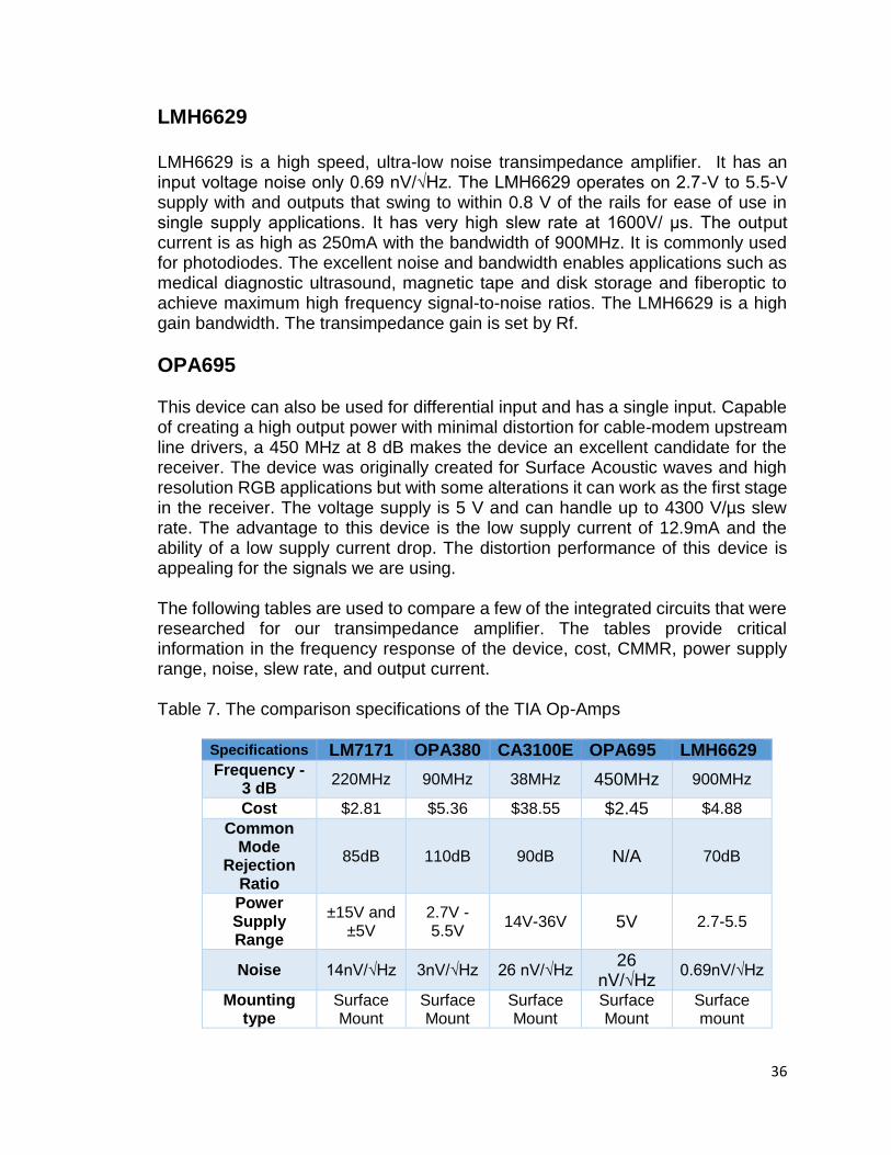
36
LMH6629 LMH6629 is a high speed, ultra-low noise transimpedance amplifier. It has an input voltage noise only 0.69 nV/√Hz. The LMH6629 operates on 2.7-V to 5.5-V supply with and outputs that swing to within 0.8 V of the rails for ease of use in single supply applications. It has very high slew rate at 1600V/ μs. The output current is as high as 250mA with the bandwidth of 900MHz. It is commonly used for photodiodes. The excellent noise and bandwidth enables applications such as medical diagnostic ultrasound, magnetic tape and disk storage and fiberoptic to achieve maximum high frequency signal-to-noise ratios. The LMH6629 is a high gain bandwidth. The transimpedance gain is set by Rf.
OPA695 This device can also be used for differential input and has a single input. Capable of creating a high output power with minimal distortion for cable-modem upstream line drivers, a 450 MHz at 8 dB makes the device an excellent candidate for the receiver. The device was originally created for Surface Acoustic waves and high resolution RGB applications but with some alterations it can work as the first stage in the receiver. The voltage supply is 5 V and can handle up to 4300 V/µs slew rate. The advantage to this device is the low supply current of 12.9mA and the ability of a low supply current drop. The distortion performance of this device is appealing for the signals we are using. The following tables are used to compare a few of the integrated circuits that were researched for our transimpedance amplifier. The tables provide critical information in the frequency response of the device, cost, CMMR, power supply range, noise, slew rate, and output current.
Table 7. The comparison specifications of the TIA Op-Amps
Specifications LM7171 OPA380 CA3100E OPA695 LMH6629 Frequency -
3 dB 220MHz 90MHz 38MHz 450MHz 900MHz
Cost $2.81 $5.36 $38.55 $2.45 $4.88
Common Mode
Rejection Ratio
85dB 110dB 90dB N/A 70dB
Power Supply Range
±15V and ±5V
2.7V - 5.5V
14V-36V 5V 2.7-5.5
Noise 14nV/√Hz 3nV/√Hz 26 nV/√Hz 26
nV/√Hz 0.69nV/√Hz
Mounting type
Surface Mount
Surface Mount
Surface Mount
Surface Mount
Surface mount
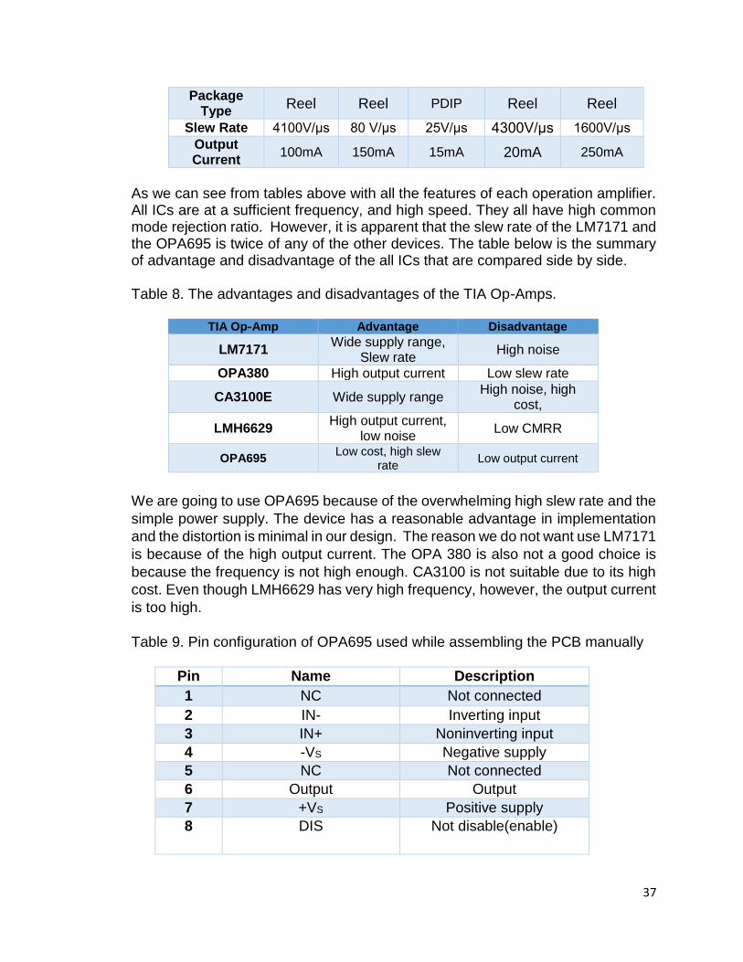
37
Package Type
Reel Reel PDIP Reel Reel
Slew Rate 4100V/μs 80 V/μs 25V/μs 4300V/μs 1600V/μs
Output Current
100mA 150mA 15mA 20mA 250mA
As we can see from tables above with all the features of each operation amplifier. All ICs are at a sufficient frequency, and high speed. They all have high common mode rejection ratio. However, it is apparent that the slew rate of the LM7171 and the OPA695 is twice of any of the other devices. The table below is the summary of advantage and disadvantage of the all ICs that are compared side by side. Table 8. The advantages and disadvantages of the TIA Op-Amps.
TIA Op-Amp Advantage Disadvantage
LM7171 Wide supply range,
Slew rate High noise
OPA380 High output current Low slew rate
CA3100E Wide supply range High noise, high
cost,
LMH6629 High output current,
low noise Low CMRR
OPA695 Low cost, high slew
rate Low output current
We are going to use OPA695 because of the overwhelming high slew rate and the
simple power supply. The device has a reasonable advantage in implementation
and the distortion is minimal in our design. The reason we do not want use LM7171
is because of the high output current. The OPA 380 is also not a good choice is
because the frequency is not high enough. CA3100 is not suitable due to its high
cost. Even though LMH6629 has very high frequency, however, the output current
is too high.
Table 9. Pin configuration of OPA695 used while assembling the PCB manually
Pin Name Description
1 NC Not connected
2 IN- Inverting input
3 IN+ Noninverting input
4 -VS Negative supply
5 NC Not connected
6 Output Output
7 +VS Positive supply
8 DIS Not disable(enable)

38
3.2.3 Differential Driver
A differential driver takes a single ended signal, and converts it into a differential output signal. This is a possible device for taking the output of an optoelectronic component such as a photodiode, and producing a data signal that can be amplified for the Ethernet output. This device will take a single ended input signal, Vin, and generates two output signals, Vout+ and Vout-. The differential output signal, Vdiff, is the difference between the two single-ended output signals. A few possible considerations for this role are compared below.
AD8131 The AD8131 is the compliment chip to the AD8130. The AD8131 is used for single-ended input to differential output driver. The AD8131 differs from conventional op-amps in that it has two outputs whose voltages move in opposite directions. It has fix gain of 2 without using any external components. It has a good advantage over other op-amp for driving signals over long line transmission. AD8131 is a differential driver that will provide a transmission of high speed signals over low-cost twisted pair cables. It is used for analog video signals or for other high-speed data transmission. It is suited for driving Cat5 twisted pair with minimal line attenuation. It has considerable cost and performance improvements over discrete line driver solutions. The AD8131’s differential output also helps balance the input for differential ADCs, optimizing the distortion performance of the ADCs. It has very high slew rate and high frequency. The power supply range is from 2.7V to 5V which works just fine.
MAX4448 MAX4448 is a small signal bandwidth amplifier. It is a single ended to differential line driver that is designed for high speed communication. The device is capable of creating a transmitter signal over twisted pair cable. It is well-suited to drive twisted-pair cables. It uses a current feedback for greater bandwidth. It has bandwidth up to 330MHz however, the slew rate is not suitable for our application. The low-power enable mode reduces current consumption below 5.5mA and places the outputs in a high-impedance state. It can deliver differential output swings of ±6.2V from ±5V. One good thing about this device is that it has excellent differential gain/phase and noise specifications make these amplifiers ideal for a wide variety of video and RF signal-processing and transmission applications. The MAX4448 is stable with minimum gain of 2.
THS4120

39
THS4120 can be used in a simple single ended to differential conversion. The THS4120 has power supply at 3.3V, with 100 MHz frequency at -3 dB, with a common mode rejection ratio of a range of 64-96 dB. The THS4120 features a power-down pin which lowers the quiescent current from 11 mA down to 120 µA, ideal for reducing system power. The slew rate of THS4120 is low, only 50 V/μs. The input voltage noise is 5.4 nV/√Hz at 10 kHz. The power supply range is going to be a problem for this IC. The device outputs only 3.3V max when we need 5V for transmission. The following tables are used to compare a few of the integrated circuits that were researched for our differential driver. The important fact is that we need cover single ended input to differential output as well as suitable to transfer data.
Table 10. The comparison of the differential driver specifications.
Specifications AD8131 MAX4448 THS4120 Frequency -3
dB 400MHz 330MHz 100MHz
Cost $4.72 $3.4 $6.55 Common Mode Rejection Ratio 70 dB N/A 64-96 dB
Power Supply Range
-5V -5 V 4.5V - 5.5V -3.3V
Noise 25 nV/√Hz 23nV/√Hz 5.4nV/√Hz Mounting
type Surface Mount
Surface Mount
Surface Mount
Package Type Tube Tube Tube Slew Rate 2000V/μs 50 V/μs 50V/ μs
Output Current 60mA 130mA 110mA
As we can see from tables above with all the features of each single ended to differential integrated circuits. All ICs are at a sufficient frequency, and high speed which is good for the data transmitting. The table below is the summary of advantage and disadvantage of the all ICs that are compared side by side.
Table 11. The advantages and disadvantages of the differential drivers.
Differential Drivers Advantage Disadvantage
AD8131 High frequency, high CMMR, high range of
power supply Low output current
MAX4448 High slew rate, high output current, Low
cost High noise
THS4120 High output current,
low noise, high CMMR High cost, low slew
rate, bad power supply

40
However, it may not be required if the transimpedance amplifier can feed into a comparator. Initially we thought that the AD8131 would feed into an amplifier such as the LM7171, however the differential drivers are an important consideration in making a receiver design. Table 12. Pin configuration of AD8131 used while testing.
Pin Name Description
1 -DIN Negative input
2 VOCM
Common-Mode Output Voltage. Voltage
applied to this pin sets the common-mode
output voltage with a ratio of 1:1.
3 V+ Positive Supply Voltage
4 +OUT Positive Output.
5 -OUT Negative Output
6 V- Negative Supply Voltage.
7 NC No Connect.
8 +DIN Positive Input.
3.2.4 Comparator
A comparator is essentially an op-amp operated in an open-loop configuration with either a high or low saturated output signal. As the name implies, a comparator compares two voltages to determine which is larger. The comparator is usually biased at voltages +VS and −VS, although other biases are possible. One major difference between a comparator and op-amp is that a comparator need not be frequency compensated. Frequency stability is not a consideration since the comparator is being driven into one of two states. Since a comparator does not contain a frequency compensation capacitor, it is not slew-rate-limited by the compensation capacitor as in the op-amp. Below is a comparison of a few possible comparator.
LT1713 LT1713 is single/dual comparator featuring rail-to-rail input, and rail-to-rail complementary output. It is 7ns at 20mV overdrive and 8.5ns at 5mV overdrive. The comparator has low power input which is 5mA. LT1713 is designed to be used in variety of systems such as high speed automatic test equipment, high speed triggers, line receivers, and window comparator. It uses a supply voltage range from 2.4V to 12V. The LT1713 has an internal TTL/CMOS compatible latches for retaining data at the outputs. Each latch holds data as long as the latch pin is held high. Latch pin hysteresis provides protection against slow moving or noisy latch signals.

41
TLV3501 TLV3501 is a push-pull output comparator featuring a 4.5 ns propagation delay. It has rail to rail input, and output, and directly drives either CMOS or TTL logic. The power supply requirements for the TLV3501 range from 2.5V to 5.5V. It also has a low supply current requirement at only 3.2 mA. It features high-speed response and includes 6 mV of internal hysteresis for improved noise immunity with an input common-mode range that extends 0.2 V beyond the power-supply rails.
MAX9691 MAX9691 is a single/dual ultra-fast ECL comparator capable of very short propagation delay (1.2 ns). The power supply requirements range from -5.2V to 5V. It has differential inputs and complementary outputs that are fully compatible with ECL-logic levels. It is commonly used in high speed line receivers and high-speed triggers. It also features large gain-bandwidth characteristics.
TS3011 TS3011 is rail-to-rail high speed comparator features a high-speed response time. It has propagation delay of 8ns. The TS3011 offers micro power consumption as low as a few hundred microamperes, thus providing an excellent ratio of power consumption current versus response time. The TS3011 includes rail-to- rail input and push-pull outputs. The power supply operates from 2.2V to 5V. The following tables are used to compare a few of the integrated circuits that were researched for our comparator. An important factor of those comparator should have low propagation delay time. Table 13. The comparison of the comparator specifications.
Specifications LT1713 LTV3501 MAX9691 TS3011 Propagation delay time
7 ns 4.5 ns 1.2 ns 8 ns
Cost $2.55 $5.43 $5.48 $1.165 Single or Dual Single/Dual Single Single/Dual Single
Power Supply Range
2.4V to 12V
2.7V-5.5V 5V and –
5.2V 2.2V-5V
Mounting type
Surface mount
Surface mount
Surface mount
Surface mount
Package Type MSOP SOIC TSSOP ECOPACK Output Current 20 mA 74 mA 50 mA Low
As we can see from tables above with all the features of comparator. All four comparators have suitable power supply to our design. They also have short
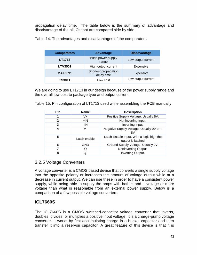
42
propagation delay time. The table below is the summary of advantage and disadvantage of the all ICs that are compared side by side. Table 14. The advantages and disadvantages of the comparators.
Comparators Advantage Disadvantage
LT1713 Wide power supply
range Low output current
LTV3501 High output current Expensive
MAX9691 Shortest propagation
delay time Expensive
TS3011 Low cost Low output current
We are going to use LT1713 in our design because of the power supply range and the overall low cost to package type and output current. Table 15. Pin configuration of LT1713 used while assembling the PCB manually
Pin Name Description
1 V+ Positive Supply Voltage, Usually 5V.
2 +IN Noninverting Input.
3 -IN Inverting Input.
4 V- Negative Supply Voltage, Usually 0V or –
5V
5 Latch enable
Latch Enable Input. With a logic high the
output is latched
6 GND Ground Supply Voltage, Usually 0V.
7 Q Noninverting Output.
8 Q- Inverting Output.
3.2.5 Voltage Converters
A voltage converter is a CMOS based device that converts a single supply voltage into the opposite polarity or increases the amount of voltage output while at a decrease in current output. We can use these in order to have a consistent power supply, while being able to supply the amps with both + and – voltage or more voltage than what is reasonable from an external power supply. Below is a comparison of a few possible voltage converters.
ICL7660S The ICL7660S is a CMOS switched-capacitor voltage converter that inverts, doubles, divides, or multiplies a positive input voltage. It is a charge-pump voltage converter. It works by first accumulating charge in a bucket capacitor and then transfer it into a reservoir capacitor. A great feature of this device is that it is

43
designed to provide a simple, compact, low-cost solution where negative or doubled supply voltages are needed for operation. It does not require an external diode when in a high voltage regime. It has wide supply voltage range are from 1.5 V to 10 V and it combines low quiescent current and high efficiency.
LTC1044A The LTC1044A provides several voltage conversion functions: the input voltage can be inverted, doubled, divided, or multiplied. It has wide operating supply voltage range which from 1.5 V to 12 V and has a 97% minimum open circuit voltage conversion efficiency as well as a 95% minimum power conversion efficiency. It also used for conversion of both 10V to ±10V Supplies and 5V to ±5V Supplies. One advantage about this device is provides several conversion functions without using inductors.
MIC2605 The MIC2605 is a constant frequency boost converter. It operates by taking a DC input voltage and regulating a higher DC output voltage. It has wide input voltage range from 4.5V to 20V. This device can be used for broadband communications, positive output regulation, local boost regulation, and DLS applications. High power density is achieved with the MIC2605/6's internal 40V/0.5A switch and Schottky diode, allowing it to power large loads in a tiny footprint. It can operate at a high frequency which is 1.2MHz and with a selective duty cycle. The duty cycle which refers to the switch on-to-off time ratio and can be calculated as follows for
a boost regulator: 𝐷 = 1 −𝑉𝑖𝑛
𝑉𝑜𝑢𝑡. The duty cycle required for voltage conversion
should be less than the maximum duty cycle of 85%.
ADM660 ADM660 is a CMOS switch capacitor voltage convertor. It is a charge-pump voltage converter that can be used to either invert the input supply voltage giving VOUT = –VIN or double it. Input voltages ranging from +1.5 V to +7 V can be inverted into a negative –1.5 V to –7 V output supply. The voltage conversion task is achieved using a switched capacitor technique using two external charge storage capacitors. It has extremely high output current which is 100mA. It is used for handheld instruments, portable computers, remote data acquisition, and op-amp power supplies. In order to optimize capacitor size, it uses a frequency control input pin to select 25 kHz or 120 kHz charge-pump operation. The following tables are used to compare those voltage convertors.

44
Table 16. The comparison of the voltage converter specifications.
Specifications ICL7660S LTC1044A MIC2605 ADM660
Inverting Mode Yes Yes Yes Yes
Cost $3.01 $5.43 $1.18 $2.94
Voltage conversion efficiency
98% 97% 99% N/A
Power Supply Range
1.5V -10 V 1.5V-12V 4.5V-20 1.5V-7V
Mounting type Through
hole Surface mount
Surface mount
Through hole
Package Type Tube Reel Reel TSSOP Output Current 20mA 20mA low 100mA
As we can see from tables above with all the features of voltage convertor. All four can be in inverting mode. They have very high voltage conversion efficiency. They are wide power supply ranges. The table below is the summary of advantage and disadvantage of the all ICs that are compared side by side.
Table 17. The advantages and disadvantages of the voltage converters.
Voltage Converter Advantage Disadvantage
MAX1044 Wide power supply Low output current
LTC1044 Wide power supply
range Low output current,
expensive
MIC2605 Lowest cost, highest
efficiency, Low output current
ADM440 High output current Voltage conversion
efficiency is high
We are going to use MIC2605 in our design because of its ability to change voltages. In our application, the laser will require a relatively low input current and the power supply need only regulate a reliable output voltage. The operational amplifiers, and differential drivers should be able to manipulate that voltage into a suitable regime for operation.
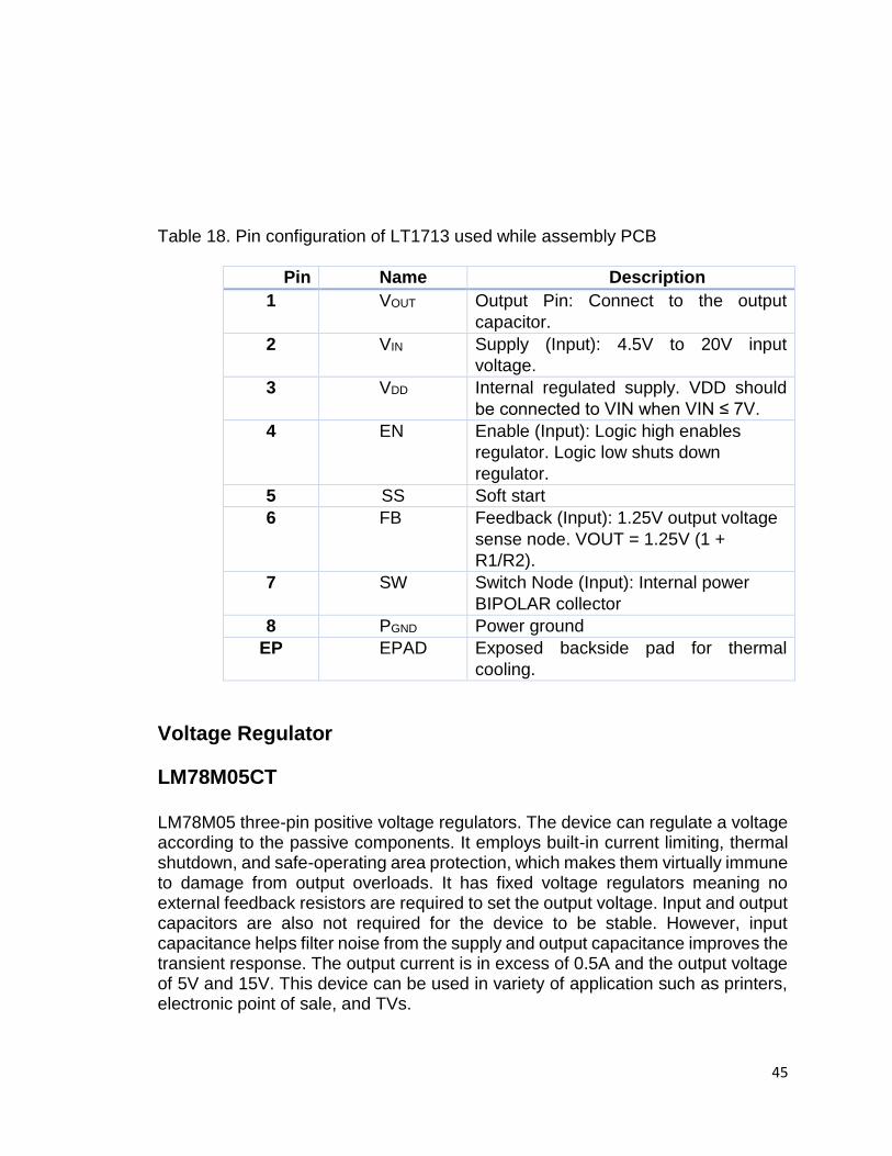
45
Table 18. Pin configuration of LT1713 used while assembly PCB
Pin Name Description
1 VOUT Output Pin: Connect to the output
capacitor.
2 VIN Supply (Input): 4.5V to 20V input
voltage.
3 VDD Internal regulated supply. VDD should
be connected to VIN when VIN ≤ 7V.
4 EN Enable (Input): Logic high enables
regulator. Logic low shuts down
regulator.
5 SS Soft start
6 FB Feedback (Input): 1.25V output voltage
sense node. VOUT = 1.25V (1 +
R1/R2).
7 SW Switch Node (Input): Internal power
BIPOLAR collector
8 PGND Power ground
EP EPAD Exposed backside pad for thermal
cooling.
Voltage Regulator
LM78M05CT LM78M05 three-pin positive voltage regulators. The device can regulate a voltage according to the passive components. It employs built-in current limiting, thermal shutdown, and safe-operating area protection, which makes them virtually immune to damage from output overloads. It has fixed voltage regulators meaning no external feedback resistors are required to set the output voltage. Input and output capacitors are also not required for the device to be stable. However, input capacitance helps filter noise from the supply and output capacitance improves the transient response. The output current is in excess of 0.5A and the output voltage of 5V and 15V. This device can be used in variety of application such as printers, electronic point of sale, and TVs.
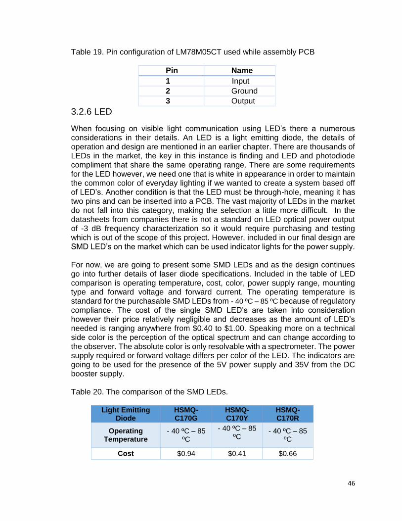
46
Table 19. Pin configuration of LM78M05CT used while assembly PCB
Pin Name
1 Input
2 Ground
3 Output
3.2.6 LED
When focusing on visible light communication using LED’s there a numerous considerations in their details. An LED is a light emitting diode, the details of operation and design are mentioned in an earlier chapter. There are thousands of LEDs in the market, the key in this instance is finding and LED and photodiode compliment that share the same operating range. There are some requirements for the LED however, we need one that is white in appearance in order to maintain the common color of everyday lighting if we wanted to create a system based off of LED’s. Another condition is that the LED must be through-hole, meaning it has two pins and can be inserted into a PCB. The vast majority of LEDs in the market do not fall into this category, making the selection a little more difficult. In the datasheets from companies there is not a standard on LED optical power output of -3 dB frequency characterization so it would require purchasing and testing which is out of the scope of this project. However, included in our final design are SMD LED’s on the market which can be used indicator lights for the power supply. For now, we are going to present some SMD LEDs and as the design continues go into further details of laser diode specifications. Included in the table of LED comparison is operating temperature, cost, color, power supply range, mounting type and forward voltage and forward current. The operating temperature is standard for the purchasable SMD LEDs from - 40 ºC – 85 ºC because of regulatory compliance. The cost of the single SMD LED’s are taken into consideration however their price relatively negligible and decreases as the amount of LED’s needed is ranging anywhere from $0.40 to $1.00. Speaking more on a technical side color is the perception of the optical spectrum and can change according to the observer. The absolute color is only resolvable with a spectrometer. The power supply required or forward voltage differs per color of the LED. The indicators are going to be used for the presence of the 5V power supply and 35V from the DC booster supply. Table 20. The comparison of the SMD LEDs.
Light Emitting Diode
HSMQ-C170G
HSMQ-C170Y
HSMQ-C170R
Operating Temperature
- 40 ºC – 85 ºC
- 40 ºC – 85 ºC
- 40 ºC – 85 ºC
Cost $0.94 $0.41 $0.66
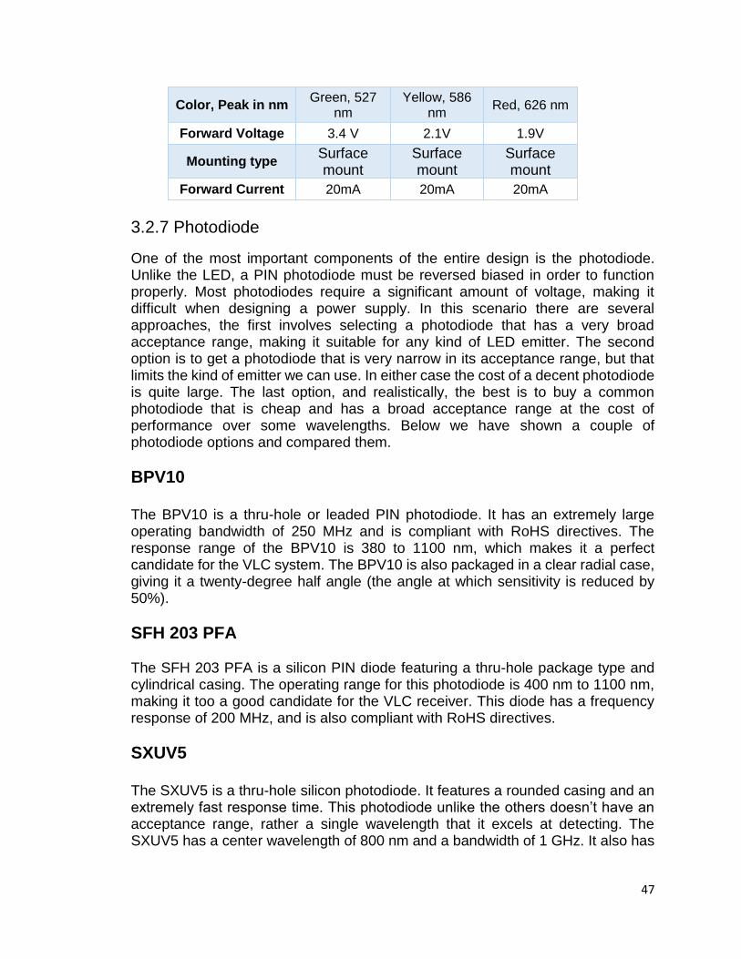
47
Color, Peak in nm Green, 527
nm Yellow, 586
nm Red, 626 nm
Forward Voltage 3.4 V 2.1V 1.9V
Mounting type Surface mount
Surface mount
Surface mount
Forward Current 20mA 20mA 20mA
3.2.7 Photodiode
One of the most important components of the entire design is the photodiode. Unlike the LED, a PIN photodiode must be reversed biased in order to function properly. Most photodiodes require a significant amount of voltage, making it difficult when designing a power supply. In this scenario there are several approaches, the first involves selecting a photodiode that has a very broad acceptance range, making it suitable for any kind of LED emitter. The second option is to get a photodiode that is very narrow in its acceptance range, but that limits the kind of emitter we can use. In either case the cost of a decent photodiode is quite large. The last option, and realistically, the best is to buy a common photodiode that is cheap and has a broad acceptance range at the cost of performance over some wavelengths. Below we have shown a couple of photodiode options and compared them.
BPV10 The BPV10 is a thru-hole or leaded PIN photodiode. It has an extremely large operating bandwidth of 250 MHz and is compliant with RoHS directives. The response range of the BPV10 is 380 to 1100 nm, which makes it a perfect candidate for the VLC system. The BPV10 is also packaged in a clear radial case, giving it a twenty-degree half angle (the angle at which sensitivity is reduced by 50%).
SFH 203 PFA The SFH 203 PFA is a silicon PIN diode featuring a thru-hole package type and cylindrical casing. The operating range for this photodiode is 400 nm to 1100 nm, making it too a good candidate for the VLC receiver. This diode has a frequency response of 200 MHz, and is also compliant with RoHS directives.
SXUV5 The SXUV5 is a thru-hole silicon photodiode. It features a rounded casing and an extremely fast response time. This photodiode unlike the others doesn’t have an acceptance range, rather a single wavelength that it excels at detecting. The SXUV5 has a center wavelength of 800 nm and a bandwidth of 1 GHz. It also has

48
a large half angle at forty degrees. The next two tables provide a specifications comparison between the three photodiodes. Table 21. The comparison of the photodiode candidates.
Specifications BPV10 SFH 203 SXUV5
Operating Temperature
- 10 ºC – 40 ºC - 10 ºC – 40 ºC - 10 ºC – 40 ºC
Cost $1.11 $0.29 $363.95
Response, Peak in nm
400 – 1100 nm, 950 peak
400 – 1000 nm, 900 peak
Near IR, 800 nm
Reverse Voltage 5 – 60 v 5 - 50 V 20 V
Mounting type Through hole Through hole Through hole
Forward Current 70 uA 9.5 uA 10 uA
Frequency Response 250 MHz 270 Mhz 1 GHz
The advantages that we are looking for in this design are the frequency response and significant price reduction. Table 22. The advantages and disadvantages of the photodiodes
Photodiode Advantage Disadvantage
BPV10 Large response range,
good output current
High reverse voltage to be effective
SFH 203 Cheapest, with good
range Low output current
SXUV5 Low reverse voltage, very fast response
Extreme price
The photodiode which will be used is the SFH 203. The cheapest with a peak able to cover visible to infrared will be an advantage in transmitter selection. The forward current of this device allows for small noise to be input into the system. Without noise, there are less integrated circuits needed for compensation.
3.2.8 Laser Criteria
In the market, there is a vast number of products which can be used as a functioning light transmitting laser. The laser is an optical device which can transmit an electrical signal by employing a two sets of modulation techniques, internal/direct modulation or external modulation.

49
The internal modulation techniques arise from the operation of the change in intensity from the changing of the supplied voltage or current to the operating point of the laser. External modulation techniques include changing the optical phase, polarization, or amplitude by an adjacent electro-optical device that can split and create two or more separate beams which have phases that constructively or destructively interfere. The internal modulation technique is the method chosen because of the inherent analog characteristics which it contains. Internal modulation also known as gain switching is pumping the population of electrons briefly over the threshold for light output in very short intervals. Although the analog signal may be unreliable in data transmission, the receiver system has a comparator which recreates this signal into a discrete structure for the TCP/IP protocols which are mentioned in chapter 6. In our project due to time constrains and limitations of budgeting, semiconductor laser such as VCSEL, Distributed feedback, QCL and Fabry-Perot lasers are not going to align with our construction abilities. The laser which we will use have a packaging type where they are built with an internal heat sink metal and not an electrically pumped heat sink. We will not select butterfly packaged lasers which are made with 14 pins for temperature control and electrical control, our laser will only be able to be directly modulated with the electric current. The laser we are choosing is going to be in the visible spectra in order to have an easier time aligning the diode to the photodetector and for the actual presentation to an audience. In order to narrow down the selection the criteria must be established according to some of the following characteristics: operating temperature, so we can have a good sense of how long the device can operate before overheating, cost because it is important to keep the budget in mind, operating voltage or turn on voltage which the device can turn on, working current to know how much current we should limit the device to, wavelength to know the spectral distribution of the device, output power limit to know how much power the device emits according to the maximum output rating and finally the mounting type to know how to construct the device in the product integration. Jameco Valuepro 154145 This 650 nm laser has been designed to have a manufactured internal heat sink to dissipate the heat generated from the output. The operating voltage is in the range of the transmission in 3 V making it an ideal candidate, and the current is within the range we need being < 40 mA. The required current is a 30 mA over threshold where it is in the linear region with ± 10 % capabilities. The through hole of 2 pins is the desired mounting type because there is an internal ground. Lilly Electronics 532MD-30-5V-TTL
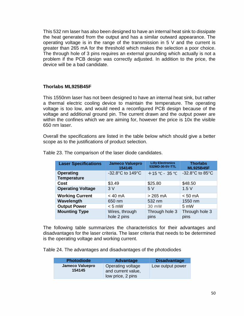
50
This 532 nm laser has also been designed to have an internal heat sink to dissipate the heat generated from the output and has a similar outward appearance. The operating voltage is in the range of the transmission in 5 V and the current is greater than 265 mA for the threshold which makes the selection a poor choice. The through hole of 3 pins requires an external grounding which actually is not a problem if the PCB design was correctly adjusted. In addition to the price, the device will be a bad candidate. Thorlabs ML925B45F This 1550nm laser has not been designed to have an internal heat sink, but rather a thermal electric cooling device to maintain the temperature. The operating voltage is too low, and would need a reconfigured PCB design because of the voltage and additional ground pin. The current drawn and the output power are within the confines which we are aiming for, however the price is 10x the visible 650 nm laser. Overall the specifications are listed in the table below which should give a better scope as to the justifications of product selection. Table 23. The comparison of the laser diode candidates.
Laser Specifications Jameco Valuepro 154145
Lilly Electronics 532MD-30-5V-TTL
Thorlabs ML925B45F
Operating Temperature
-32.8°C to 149°C +15 ℃ - 35 ℃ -32.8°C to 85°C
Cost $3.49 $25.80 $48.50
Operating Voltage 3 V 5 V 1.5 V
Working Current < 40 mA > 265 mA < 50 mA
Wavelength 650 nm 532 nm 1550 nm
Output Power < 5 mW 30 mW 5 mW
Mounting Type Wires, through hole 2 pins
Through hole 3 pins
Through hole 3 pins
The following table summarizes the characteristics for their advantages and disadvantages for the laser criteria. The laser criteria that needs to be determined is the operating voltage and working current. Table 24. The advantages and disadvantages of the photodiodes
Photodiode Advantage Disadvantage Jameco Valuepro
154145 Operating voltage and current value, low price, 2 pins
Low output power

51
Lilly Electronics 532MD-30-5V-TTL
High output power High price, high current required
Thorlabs ML925B45F
Low current and low voltage
High price
Overall, we will pick the Jameco Valuepro 154145 for the low price and electrical characteristics which go along with the electrical design that the MAX4390 can output. The laser at < 40 mA has been experimentally shown to have a threshold current at 12 mA, and therefore it can very well meet the criteria of staying within the linear range of the device and act as a gain switcher.
3.2.9 Focusing Optics
When considering a product such as VLC there are physical limiting factors that can be overcame in order to improve the overall effectiveness of the system. The idea here is to collect the beam incident on the receiving device and provide a more concentrated spot on the photo-diode. Since the two photodiodes on either end serve as the receiver for their respective devices assisting them in the collection of photons improves their efficiency. On the transmitter side of each device we will attach a collimating lens. Collimating the beam will reduce its divergence to nearly nothing allowing the beam to maintain integrity as it reaches the receiver. This is where optical elements come in. The best choice for the focusing on to the receiver is a short focal length plano-convex lens which is designed for the peak laser wavelength. The reason being is that is can take a well collimated beam and neatly readjust the beam into a smaller spot size, reducing the stray light and improving optical radiation incident onto the device. For the optics comparison, the aim of the piece is to select a F#, where it can collect more light. The "f-number," is defined as F# = F/D where F is the focal length and D is the diameter of the lens. The lens which would produce the smallest spot size from a collimated monochromatic input beam would be a plano-convex lens because the surface of a biconvex lens will have one surface which will want to expand the beam and the other will compensate, however with a plano-convex this is going to happen. The F# or speed of a lens can relate to the beam divergence or convergence in a spot size which can be approximated as 𝜃 = tan-1
F/D = 𝜆
𝜋𝜔𝑜 so a smaller F# can create a smaller spot size and thus more reception
of light. For an example on lens quickness, a particular lens seen in Fig. 3.17, this lens is from Newport Corporation entitled “Plano-Convex Lens, N-BK7, 6.0 mm Diameter, 17 mm EFL, Uncoated.” The F# of this lens is trivially 2.833 which would increase in “fastness” if the diameter was larger. The lens can be simulated in an optical design software called Opticstudio, which allows for the user to make an infinite sum of an optical train lenses and see the results. The simulator is only a calculator
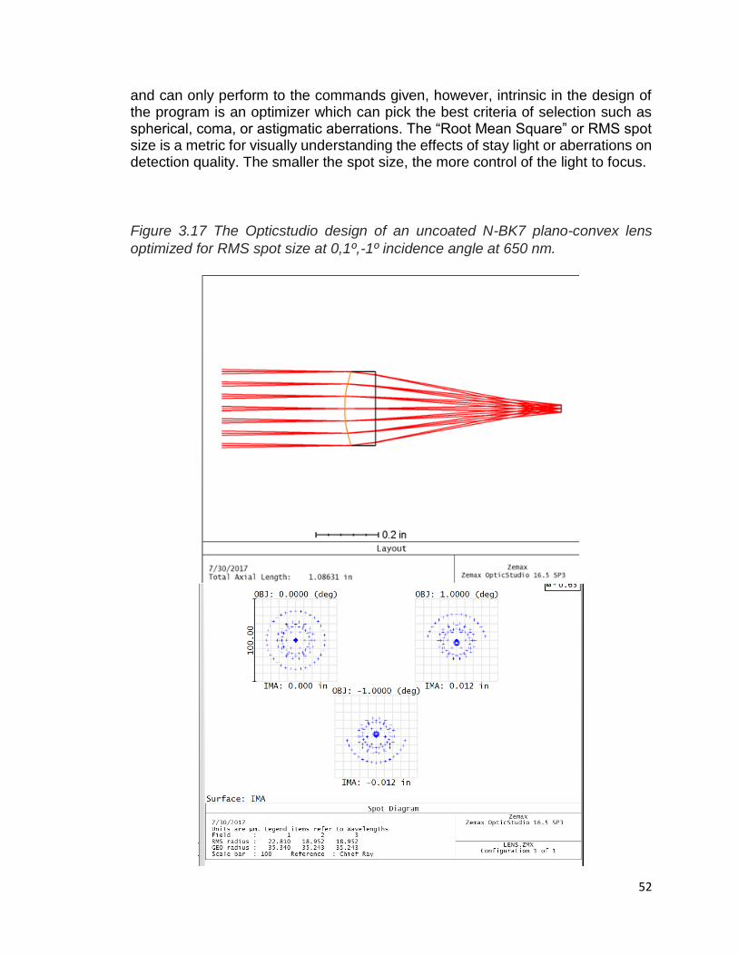
52
and can only perform to the commands given, however, intrinsic in the design of the program is an optimizer which can pick the best criteria of selection such as spherical, coma, or astigmatic aberrations. The “Root Mean Square” or RMS spot size is a metric for visually understanding the effects of stay light or aberrations on detection quality. The smaller the spot size, the more control of the light to focus.
Figure 3.17 The Opticstudio design of an uncoated N-BK7 plano-convex lens
optimized for RMS spot size at 0,1º,-1º incidence angle at 650 nm.

53
For the transmitter side, a simple aspheric plano-convex lens will do the trick of collimating the beam. In this scenario, the lens would be placed opposite the direction of the receiving lens so that the laser beam is incident on the planar side of the lens. An aspheric lens as the name suggests is shaped in a way such that the surface is not one single radius, nor is it continuous, as seen below.
Fig. 3.18 An aspheric lens (Courtesy of Edmund optics)
Generally, aspheres are optimized for non-continuous incident angularity, whereas the beam may not be as efficient in power at all angles equally meaning aspheres are also intolerant to spherical aberrations, some possible lens choices have been listed and are compared below. LA1116 The LA1116 is a plano-convex lens made from BK7 type glass manufactured by Thorlabs. It has a diameter of 6 mm and a focal length of 10 mm, therefore it has an F# = 1.667 which is fast enough for our system. This lens is uncoated and has a wavelength range of 350 nm to 1800 nm where the transmission of the lens is over 90% light passing through for N-BK7, and a 10 mm thickness sample. The lens is thickest in the center at just 2.5 mm and 1.5 mm at the edges with around a 5% thickness tolerance. Therefore the 90% transmission rate is probably higher, meaning more power to the respective devices. This ensures that the lens will not impede the design of the device box. This lens is RoHS compliant and is sold as is not mounted. The cost of the LA1116 is $20.30.

54
4. Related Standards and Realistic Design Constraints
4.1 Standards Standards are a set of specific characteristics that guide product and system design in the developed world. While standards are not enforceable by law, the point of them is to ensure that new products meet a certain level of safety, performance, reliability, compatibility etc. As a whole, standards provide common ground between different companies, and organizations across the world. For the VLC project, the IEEE has a number of standards that are relevant, as well as UL, and RoHS. In this section we discuss the various standards related to the design and implementation of the VLC project as well as their impact on the project.
4.1.1 IEEE 802.3i
The Institute of Electrical and Electronics Engineers, sometimes referred to as “I triple e”, is a worldwide professional association consisting of scientists and engineers. The IEEE is a nonprofit organization that provides a number of services from publishing, to education, holding conferences, to maintaining societies and developing standards. The IEEE 802 standard is one of the most recognized across the world, it relates to local and metropolitan area networks. The 802.3 sub-standard is the overall category defining standards for the physical layer of local and wide area networks. For the Visible Light Communication project the 802.3i standard is particularly important. This standard was published in 1990 and is commonly known as 10 Base-T, it defines the requirements for 10 Mbit/s speed across twisted pair cables. 10 Base-T Ethernet uses category 3 cabling and is encoded in Manchester coding, the channel bandwidth is 10 MHz and cabling must be rated for at least 16 MHz.
4.1.2 Design Impact of IEEE 802.3i standard
The IEEE 802.3i standard has huge impacts on the VLC system. Because the 802 category is accepted worldwide as local and wide area network standards there is no room for selection in regards to how our data is carried from the service provider to our equipment. Because of this, the signals that are available to try to convert to light are already predefined. For instance we can choose to convert a 100Base-T signal, a 10Base-T signal, a 1000Base-X, etc. into a driving signal for our transmitters. With that being said the component selection is also limited to electronics that are capable of receiving and transmitting high speed electrical signals.

55
4.1.3 IEEE 802.15.7
The 802.15 group of standards covers wireless personal area networks. The 802.15.7 subset particularly relates to short-range optical wireless communications. This standard defines the guidelines for what qualifies as visible light communication. Products under this standard utilize wavelengths from 190 nm to 10000 nm, they complement existing services and provide protection from electromagnetic interference.5
4.1.4 Design Impact of IEEE 802.15.7
The 802.15.7 standard effects the VLC project in terms of how the device performs and is implemented. By the standards definition the actual data link between two VLC devices must provide no EM interference. This limits how we can modulate the LED or laser diode. For instance we could not use amplitude modulation, because of its potential to interfere with other ongoing transmissions. So in this case the best option is to impose the signal directly onto a DC bias and use a type of OOK modulation.
4.1.5 UL 1310
UL (Underwriters Laboratories) is an organization recognized by the American National Standards Institute for created standards. UL 1310 is a safety requirement for class 2 power units, which are defined as units that utilize an isolating transformer and have a maximum rating of 42.4 volts AC. In terms of safety requirements, the 1310 standard ensures that device enclosures are rigid and able to resist likely abuse. They also have overcurrent and over-temperature protection, as well as protection from feedback voltage. Products that have been tested and meet the UL product safety specifications are marked with the UL Logo. The UL Mark in Fig. 4.1. UL is the stamp that appears on power supply devices and is an indication that either Underwriters Laboratories or an equivalent nationally recognized testing laboratory has tested the equipment, and is an easy way for manufactures to show that their device has met safety standards. Figure 4.1. The Underwriters Laboratories signature of verification.

56
4.1.6 Design Impact of UL 1310
To be in compliance with the UL 1310 standard there are a couple design parameters that must be met. The first is the voltage rating, in the general sense this should not be a problem. However, in practice some photodiodes require a large amount of reverse voltage to be applied all the way up to 60V DC. If we were to use a simple transformer this would be an issue, because it does exceed the UL’s rating. So now we have to use some form of amplifier to convert our basic supply voltage (most likely 5V) to a significant enough value to drive the PD.
4.1.7 RoHS
RoHS stands for restriction on hazardous substances, it was first introduced in 2003 and took effect in 2006 in the European Union. The United States doesn’t have a law regulating the use of hazardous materials however similar legislation to the RoHS has been implemented by most countries around the world. In order to sell products internationally they must meet these requirements, and in compliance with the RoHS devices must have minimal levels of lead, mercury, cadmium, and chromium.
4.1.8 Design Impact of RoHS
In order to comply with the RoHS directive, we don’t have to do anything on our end. Almost all manufacturers of integrated circuits and opto-electronics already adhere to this rule. All of our parts can be found on suppliers’ websites, such as Mouser or DigiKey, who are in compliance with RoHS.
4.1.9 Power Supply Standards
The CUI has divided circuits into different classifications based on their voltage and specifications, the table below lists these.
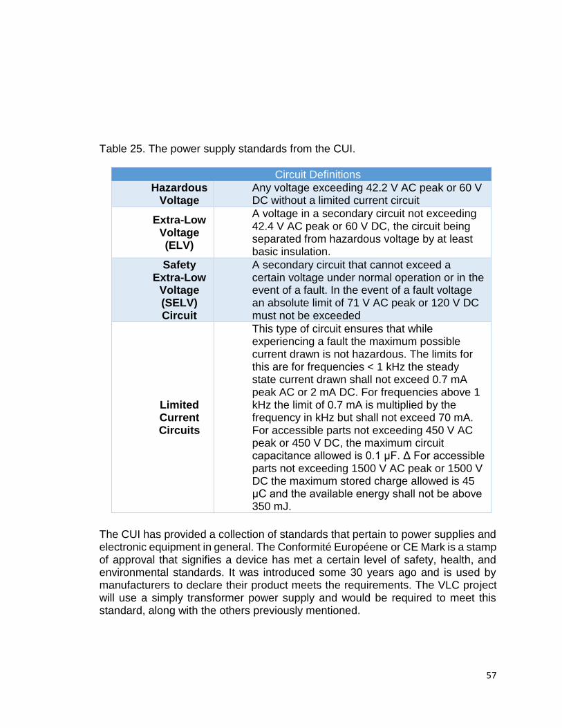
57
Table 25. The power supply standards from the CUI.
Circuit Definitions
Hazardous Voltage
Any voltage exceeding 42.2 V AC peak or 60 V DC without a limited current circuit
Extra-Low Voltage (ELV)
A voltage in a secondary circuit not exceeding 42.4 V AC peak or 60 V DC, the circuit being separated from hazardous voltage by at least basic insulation.
Safety Extra-Low
Voltage (SELV) Circuit
A secondary circuit that cannot exceed a certain voltage under normal operation or in the event of a fault. In the event of a fault voltage an absolute limit of 71 V AC peak or 120 V DC must not be exceeded
Limited Current Circuits
This type of circuit ensures that while experiencing a fault the maximum possible current drawn is not hazardous. The limits for this are for frequencies < 1 kHz the steady state current drawn shall not exceed 0.7 mA peak AC or 2 mA DC. For frequencies above 1 kHz the limit of 0.7 mA is multiplied by the frequency in kHz but shall not exceed 70 mA. For accessible parts not exceeding 450 V AC peak or 450 V DC, the maximum circuit capacitance allowed is 0.1 μF. Δ For accessible parts not exceeding 1500 V AC peak or 1500 V DC the maximum stored charge allowed is 45 μC and the available energy shall not be above 350 mJ.
The CUI has provided a collection of standards that pertain to power supplies and electronic equipment in general. The Conformité Européene or CE Mark is a stamp of approval that signifies a device has met a certain level of safety, health, and environmental standards. It was introduced some 30 years ago and is used by manufacturers to declare their product meets the requirements. The VLC project will use a simply transformer power supply and would be required to meet this standard, along with the others previously mentioned.

58
4.1.10 PCB Standards
The IPC was founded as the Institute for Printed Circuit Boards, but has since changed to the Institute for Interconnecting and Packaging Electronic Circuits. The IPC is recognized and respected across the globe for providing standards in PCB design, construction, quality, etc. The broadest coverage of the IPC PCB standards is acceptability (IPC-A-610E), providing standards for component orientation and soldering criteria, as well as surface mount IC requirements. The standard also provides a requirement for the PCB to be clean, marked, and coated, as well as Lead-free. The VLC project design does require the assembly of two separate PCBs. The PCB manufacturing is outsourced in this scenario and these standards should be met by the sub-contracted company. Our components are Lead-free by nature. The standards provided by the organizations and institutions around the world provide an underlying level of quality, safety, and reassurance that can be given to consumers. There is also a common language that is found in these standards as device manufacturing occurs across many different companies across the globe. It is important that we try to meet the criteria even in prototyping and elementary design stages.
4.1.11 Design Impact of PCB standards
Since we will not be making the PCB ourselves, the design impacts of this particular section are minimal. As long as we choose a manufacturer who is in compliance with the standards listed above we should be ok.
4.1.12 Laser Safety Standards
Classifications of lasers are controlled by an international institute called the International Electro- Technical Commission (IEC) and the Center for Devices and Radiological Health (CDRH), which is an arm of the Food and Drug Administration. The classifications for different laser systems may differ slightly in their description according to the respective institution, they have been unified.6 We are using a Class IIIa or 3R laser which is referred to as safe when handled carefully and not directly exposed to intrabeam viewing. Lasers are multifaceted devices which can have serve the user as long as the standard operating procedures are followed. The user should recognize the type of laser viewing exposure interactions which are possible in order to avoid excessive exposure. This is not a complete scope of the standards; however, we feel it is important in explaining the direct methods of avoiding risk. The following pargraph is only to be an over view and NOT considered a substitute for a knowledgeable and trained Laser Safety Officer (LSO) with the duties and responsibilities as defined in the ANSI Z136 standard published by the American National Standard Institute.

59
There are methods of understanding how viewing laser radiation can take place, however, the primary rule is avoid looking at the laser directly or from reflected mirrors. The first is intrabeam viewing which is looking at the collimated beam directly and trying to see output, this creates a small laser spot on the retina which is dangerous to the eye, only with direct medical permissions can certain lasers be used, when using visible to near infrared spectrum, (390 nm - 2500 nm), direct eye exposure should be avoided at all costs. The second is specular reflection, this is where the beam is incident on a reflective surface and the beam is the same in danger, again avoid looking directly at a reflected beam at all costs. The third way of is diffusive reflection, this is where a beam hits a rough surface and scattered light can be viewed. The scattered beam is incoherent and has a larger area hitting the retina meaning less light, however, if the diffuse reflection is too intense injury may still result. All retina injury can be serious and permanent.
4.1.13 Design Impact of Laser Safety Standard
In order to be compliant with laser safety standards we must adjust the design of the device accordingly. It would be easy to use a laser diode that has a high output, that would take a lot of strain off the photodiode, and would increase the working distance considerably. However, in order to be safe, it's best to use a laser diode that is relatively low in power specifically < 5 mW which means that incident exposure for under ¼ seconds is not harmful. In order to compensate focusing elements can be used.
4.1.14 Software Standards C++
The International Organization for Standardization (ISO) is responsible for releasing standards for the C++ programming language. The current standard is ISO/IEC 18882:2014, informally known as C++14, it was introduced in 2014. It is important for the ISO to continually update the C++ standard as the core language and library constantly expand to meet the requirements of technology. This specific standard is meant to instruct programmers on the implementation process of the standard. In addition, each new release of the standard aims to improve known issues with previous versions as well as expand the capabilities. C++ is a general language and is paramount to the operation of many electronic devices and machinery.
4.1.15 Design Impact of C++ Standard
The main focus of the software in this project is to analyze data being passed through the VLC system, to verify that the system is actually acting as an internet enabled device. In order to do this a program must be written in a compiler and run on the computer making use of the VLC system. With that being said a compiler that accepts C++ is required to make this happen, for this project our computer engineer will be using Visual Studio to carry out this task.

60
4.1.16 Electronics Housing Standards
This standard is provided by the National Electrical Manufacturers Association, it details the requirements for safe electronic housings. Available for reference in the NEMA standards publication 250-2003, the document lists the types of enclosures as well as the requirements for each. Our device type according to the NEMA standard is type 5 described as an enclosure constructed for indoor use, that provides protection to personnel against hazardous parts. The enclosure must also provide protection to the equipment inside from solid foreign objects such as dirt, settling airborne dust, lint, fibers, etc.
4.1.17 Design Impact of Housing Standard
In order for the VLC project to look professional in its design and appearance a
housing will be constructed for the electronics to reside in. Our design and final
product will follow the standards provided by NEMA and provide the electronics
with protection from their environment. In order to do so we need to identify the
type of material we will make the housing out of and then identify a
company/service to provide it. The housing will most likely be plastic, and will be
3D printed. Our housing design can be found in chapter 5 along with a detailed
account of its features.
4.2 Design Constraints With the design of any new product for system there comes constraints. Whether these are customer defined, budgetary, legal, etc. each constraint must be taken into account before a complete set can be created. For most products, there are checks and balances between each constraint, for instance a larger budget often results in better components. Or a legal constraint might affect the manufacturability of the product. In all constraints are a realistic part of new design, below is a collection of the constraints that effect the VLC project and it’s outcome.
4.2.1 Economic and Time Constraints Currently internet access can be obtained by a few dollars’ worth of hardware and a subscription to an ISP, so our VLC system needs to be competitive in price. For VLC, we wanted to keep the budget under $300, this is an economic constraint that limits what kinds of components we can buy, and how much the product could retail for. Comparatively, however, current LiFi systems can run upwards of $2000. With that being said there is an obvious tradeoff between the speed of a system and the project budget. In either case VLC provides energy efficiency and is especially applicable in commercial environments where buildings are lit the majority of the time. If implemented on a wide scale VLC would have a huge impact on energy and cost savings for anyone switching from a standard wireless access router.

61
Time is a very real constraint that effects every aspect of life not just engineering, for this instance though, our time is limited to several months. We started this project in the middle of May, and were given just 12 weeks to design and prototype. Following that period there is an additional 16 weeks to turn the prototype into a working product, where it will then be presented and reviewed by faculty. For this project speed is one of the most important features of the system, time directly effects that characteristic in this situation. For instance, improving the speed of VLC is not as simple as upgrading hardware, because it is a complimentary system it requires research and must be treated as an entirely new product. Since time can never be gotten back it is important to create deadlines and goals to be upheld so that you have constant knowledge of where you stand in terms of completion.
4.2.2 Environmental, Health and Safety Constraints Environmental constraints can be very taxing on a company when designing a new product. You must take into account whether or not your product produces pollution (air, water, or noise), what kind of impact it has on its direct surroundings, and what kind of waste occurs in the process. For VLC, there are no emissions such as gasses, wastes, noise, vibrations etc. However, there are manufacturing concerns as with any electronic device. As previously mentioned some electronics use hazardous materials and are limited by RoHS regulation. Or VLC system uses silicon and copper based component and does not contain any hazardous material. VLC systems also save energy, using light as a transmitter and Ethernet as a power supply you eliminate an unnecessary cost of a Wi-Fi router. In regards to operation VLC does not produce any kind of electromagnetic interference, because the carrier signal is in the THz region it is safe for EM sensitive environments. Health and Safety constraints can really be combined into a single category of limiting factors. When considering these two constraints there are two primary groups, the sellers and the consumers. In terms of installation there are no health and safety concerns that are inherit to the device. When being operated, there are no health and safety concerns that need to be considered by the consumer. Our design, as previously mentioned, does not use hazardous materials, and produces no wastes including (noise, gasses etc.). VLC operates using LEDs in the visible spectrum, and modulates at a MHz rate, so there are no concerns for those who have epilepsy or similar conditions. In all VLC is a very safe technology for users.
4.2.3 Environmental Spectral Window Distribution The ability to propagate light over a certain distance will dictate how far the information can travel. Neglecting the efficiency of the detector and optical efficiency in the transmitter, the Power received is equivaled to
𝑃𝑅 =𝑃𝑇𝐴𝑅
(𝜃𝑑)2 exp (−𝛼𝑑) where 𝑃𝑇 is power transmitted, 𝐴𝑅 is the receiver area, 𝜃 is
the divergence angle, 𝑑 is the distance traveled and finally 𝛼 is the attenuation of

62
decibels/km. The transmission properties from the atmosphere in the near infrared wavelength range under clear weather conditions is in the figure below7, forming the basis for a wavelength selection guide in the outdoors. For example, the windows located near 850 nm, 1060 nm, 1250 nm, 1560 nm have very low attenuation and give the group a wide selection.
Figure 4.2. The attenuation coefficient as a function of wavelength.
4.2.4 Social, Political, and Ethical Constraints
Social and Political constraints can be viewed as a design favoring one group of people and against another. They can include a product that is against government laws and regulations, they can include a product that relies on publicly funded works or services. We can conclude that there are no political constraints that are obvious or apparent to the VLC project. Social constraints are in the same boat, VLC is a product meant for everyone and there are no prerequisites to using it. Ethical constraints are considered when designing the product and are taken into account in terms of how the product or service will affect the safety and/or health of its users/workers/competitors. For instance using radioactive materials, using designs or data that are protected under copyright, sacrificing safety for appearance or cheaper materials. In some cases of VLC infrared LEDs may be used for the uplink. IR LEDs that are in the lower region say 700-1400 nm can be dangerous to the retina and eye if overexposure occurs. Safe IR LEDs are above 1400 nm because the majority of the wave dissipates in the water of the eye and isn’t focused onto the retina. However safe IR LEDs are quite expensive, and in many cases, are not used in products.

63
4.2.5 Manufacturability and Sustainability Constraints
Some manufacturing properties include nanoscopic scale, high stiffness and rigidity, no contact surfaces, no machining vibration, extremely accurate natural frequencies, specific alloys/metals etc. The equipment to manufacture such devices is very expensive. For our VLC project we have chosen pre-fabricated parts, and once a PCB is created it will feature a single power connection, and a single Ethernet port. Our design also features plastic casing, so there is no need for alloys or other special metals. Sustainability is not only a constraint but also a very real selling point for any product. Nowadays people want to know that their things are going to last, without having to buy replacement parts. Our design is purely solid state, meaning there are no moving parts, the system is also meant to be stationary so use of the product does not pose regular wear and tear. The component most susceptible to issues is the LED or LD itself, however today’s LEDs and LD have an active life of 25000 – 50000 hours. In perspective that’s around 3 – 6 years of constant use. In this instance VLC is meant for indoor use, so the effects of weather are not a constraint for our product.
4.3 LAN (Local Area Network) A local area network (LAN) is a group of computers and associated devices that share a common communication line or wireless link to a server. In this project, our physical link communication UTP (Unshielded Twisted Pair) plus visual light will be our medium where data will be transmitted. Typically, LAN encompasses computers and peripherals connected to a server within a distinct a distinct geographic area such as an office or a commercial establishment, in the scope of this project will be just two computers connected through the Ethernet connection.
Figure 4.3 Hierarchical LAN data transfer.
A local area network may serve as few as two or three users or several hundred users in a large office. In the figure above movement of data has gone through a number of routers to go from network 1 to network 2. Ethernet and Wi-Fi are the two primary ways to enable LAN connections, in this project will make use of Ethernet. 8
64
4.3.1 Full Duplex and Half Duplex Operation
The standards for Ethernet were originally built using a truly shared medium (a single coaxial cable connected to several stations). The same cable was used for both transmission and reception. This factor leads to smaller footprints in design of physical cables. Since the Ethernet is based on the idea of a shared medium, if a station sends a packet, everybody on the line receive it. The case of data collision exists when there is only a one-way channel in half duplex mode. In our case, 10BASE-T uses a “UTP” cable to replace coaxial cables. UTP cables allow full-duplex because they contain separate wires for transmission and reception. Therefore, that leads to the question, which is better half-duplex or Full Duplex communication.
4.3.2 Carrier Sense Multiple Access with Collision Detection (CSMA/CD)
The CSMA/CD method assesses short area networks like LAN and most notably in early Ethernet technology it was documented and developed. Again, in this project the network layer is based on the standards for 10BASE-T described in the IEEE 802.3. This method uses a carrier-sensing scheme in which a transmitting station detects collisions by sensing transmission from other stations while transmitting a frame (digital data transmission). When this collision is detected, the station stops transmitting that frame, transmits a jam signal, and the waits for a random time interval before trying to resend the frame. In a figure presented below there is a demonstration of the data collision.
Figure 4.4. Data collision framework for half-duplex functionality.
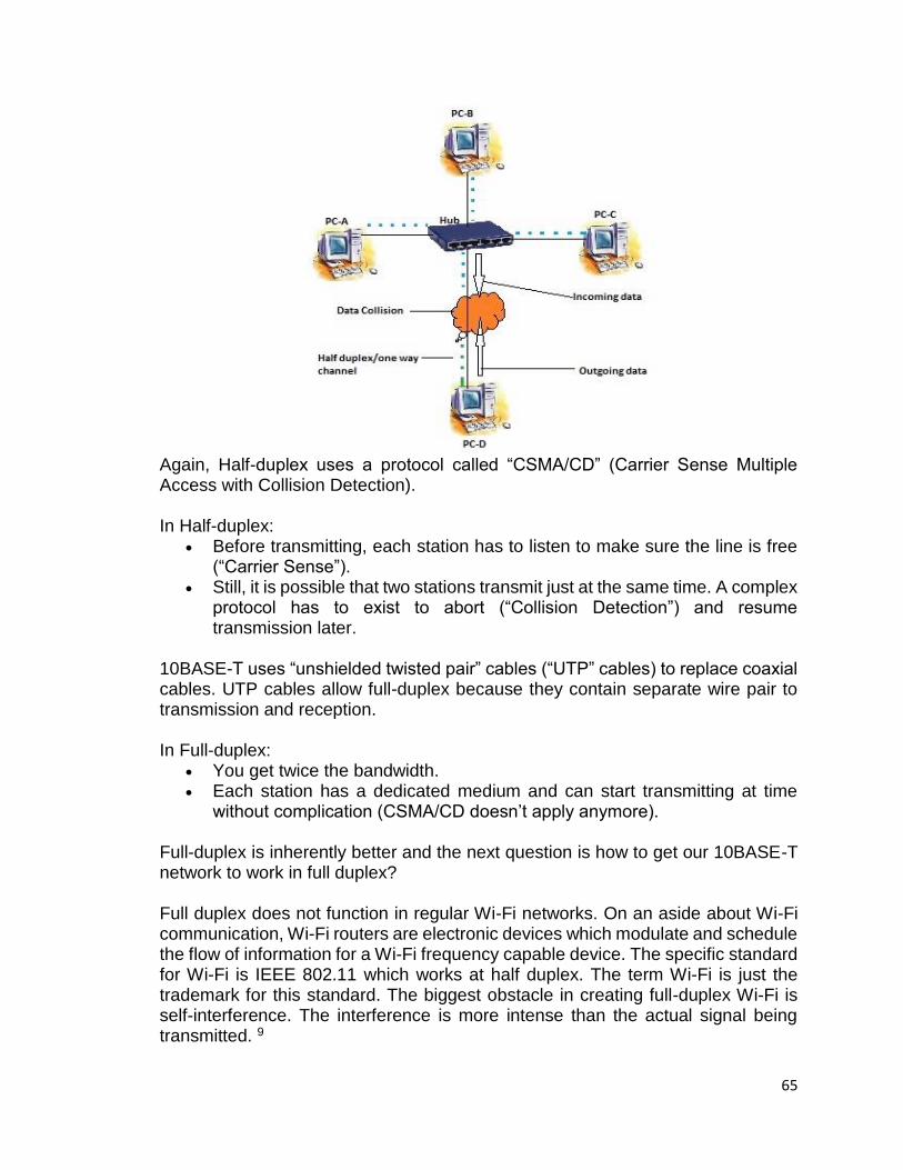
65
Again, Half-duplex uses a protocol called “CSMA/CD” (Carrier Sense Multiple Access with Collision Detection). In Half-duplex:
Before transmitting, each station has to listen to make sure the line is free (“Carrier Sense”).
Still, it is possible that two stations transmit just at the same time. A complex protocol has to exist to abort (“Collision Detection”) and resume transmission later.
10BASE-T uses “unshielded twisted pair” cables (“UTP” cables) to replace coaxial cables. UTP cables allow full-duplex because they contain separate wire pair to transmission and reception. In Full-duplex:
You get twice the bandwidth. Each station has a dedicated medium and can start transmitting at time
without complication (CSMA/CD doesn’t apply anymore). Full-duplex is inherently better and the next question is how to get our 10BASE-T network to work in full duplex? Full duplex does not function in regular Wi-Fi networks. On an aside about Wi-Fi communication, Wi-Fi routers are electronic devices which modulate and schedule the flow of information for a Wi-Fi frequency capable device. The specific standard for Wi-Fi is IEEE 802.11 which works at half duplex. The term Wi-Fi is just the trademark for this standard. The biggest obstacle in creating full-duplex Wi-Fi is self-interference. The interference is more intense than the actual signal being transmitted. 9
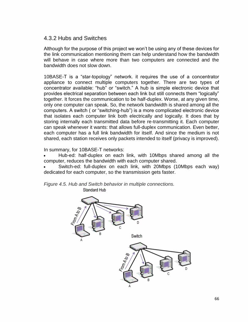
66
4.3.2 Hubs and Switches
Although for the purpose of this project we won’t be using any of these devices for the link communication mentioning them can help understand how the bandwidth will behave in case where more than two computers are connected and the bandwidth does not slow down. 10BASE-T is a “star-topology” network. it requires the use of a concentrator appliance to connect multiple computers together. There are two types of concentrator available: “hub” or “switch.” A hub is simple electronic device that provides electrical separation between each link but still connects them “logically” together. It forces the communication to be half-duplex. Worse, at any given time, only one computer can speak. So, the network bandwidth is shared among all the computers. A switch ( or “switching-hub”) is a more complicated electronic device that isolates each computer link both electrically and logically. It does that by storing internally each transmitted data before re-transmitting it. Each computer can speak whenever it wants: that allows full-duplex communication. Even better, each computer has a full link bandwidth for itself. And since the medium is not shared, each station receives only packets intended to itself (privacy is improved). In summary, for 10BASE-T networks: Hub-ed: half-duplex on each link, with 10Mbps shared among all the computer, reduces the bandwidth with each computer shared. Switch-ed: full-duplex on each link, with 20Mbps (10Mbps each way) dedicated for each computer, so the transmission gets faster.
Figure 4.5. Hub and Switch behavior in multiple connections.

67
Network Interface Card (NIC) A network interface card (NIC) is a circuit board or card that is installed in a computer so that it can be connected to a network. In network interface client-server, we implement some libraries in C# to make use of this attribute on TCP connection. Personal computers and workstations on a local area network (LAN) typically contain a network interface card specifically designed for the LAN transmission technology.
68
5 Project Hardware Design Details 5.1 Transmitter System Model The objective of this project is to design a transmitter which can transmit with a data rate of at least 5 Mbps over a considerable distance for indoor application, however there may still be abilities to have analogous transmission in outside and other environments given some sufficient testing. The idea presented is that there need to be a transmitter with enough bias and a receiver with enough amplification. The frequency response of the white LEDs listed by manufacturers are not supplied which makes the enterprise of part selection and verification hard to implement. And, further amplification on the transmitter portion is certainly possible for the brightness with a correct MOSFET design. In attempting to design our transceiver we went through a couple iteration attempts. The first iteration was trying to create a 100 Base-T system. One of the factors in prototyping this circuit was to implement the QFN package into a breadboard, and more information will be provided in a later chapter. The circuit was found through “Foundations of Visible Light Communication Circuits” (FVLCC)10. It was the initial premise for establishing our prototype. The authors of FVLCC had designs for LED’s which do not have enough luminous flux to light up a room. Furthermore, we tried and prototyped this schematic but after correspondence with the author, he recommended to us that this specific design would never be able to implement 100 Base-T VLC transmission because the schematic from the book is just a plausibility of the idea. Since there is a significant market and lucrative aspect of these systems, the RJ45 to transceiver board is harder to find in open source. The 100 Base-T transmissions definitely can be achieved, however, given our limited understanding of high speed electronics in prototyping, there was most likely errors in diagnosing the problem. There has been numerous experiments with 125+ Mbit/s NRZ and DMT modulation format white LED transmission,11,12 however they were using arbitrary wave form generators and not MLT-3 encoding. The circuit for the 100 Base-T transmission in the FVLCC made use of the MAX3967A chip however, these chips are designed for infrared transmission as is accustomed in fiber optic transmission. The next section will highlight how to use this specific LED driver in what can be used in later attempts. The main problem occurred in creating the PECL signal input. The second approach was to implement the 10 Base-T system from the FVLCC as seen in the Fig 5.1. The components were ordered for prototyping and the system still would be an analog interpreter of 10 Base-T ethernet signal onto a modulated LED. The difficulty in this set up was the use of unspecified resistor and potentiometer values. In addition, the group figured out that the LED always experienced a bias input above the standard Manchester encoding voltage which made the modulation scheme indiscernible to the photodiode on the oscilloscope even after amplification unless we used low frequencies such as 10 kHz.

69
Figure 5.1. Ethernet Connected 10Base-T VLC Transceiver device from “Foundations of Visible Light Communication Circuits” Prototype Design Premise.
5.2 Transmitting Driver Background The transceiver model for 100 Base-T using an LED driver will involve the ability to convert the Manchester encoding, or MLT-3 code from a 10 Base-T signal or 100 Base-T signals respectively into a suitable regime for an LED. The MLT-3 signal is inherently not applicable for LED illumination because it is a -1 V, 0 V, - 1 V signal at around 300 ns. Therefore, we need to convert this into a suitable signal for LED modulation. The MLT-3 needs to be converted into a NRZ or PECL signal which is suitable for LED modulation for the MAX driver. A media converter should have been used in creating this function, however, the group could not find one without purchasing an evaluation board and the ones we found as in the work by Perera13, was out of business. The idea is to build a robust system which can convert the Ethernet signals MLT-3 (analog) to digital signals as in binary or NRZI before feeding them into the MAX3967A. NRZI signals are also referred to as PECL (positive emitter-coupled logic). At the receiver, the conversion will be binary back to Ethernet. Before receiving the MLT-3 code, it should have been possible to utilize the driver.

70
5.2.1 White LED Modulation Background
The ability to use a white LED as a modulating RF transmitter is from the fact that the modulation bandwidth is capable of a few MHz and after some equalization techniques upwards of 32 MHz11. A laser diode however has magnitudes of more bandwidth to modulate because of the low dispersion and spectral distribution. The group had determined that the we should consider the quiescent point of bias operation for a commercially available LED such as the Lumileds LXR7-SW40 which can operate at 700 mA and 11.1 V. The operating point or the quiescent point for bias operation will depend upon the individual LED inputted into the system. Ideally, we could easily change our system to meet this point. From the Lumileds data sheet there is a recommendation that “The average current for each cycle does not exceed the maximum allowable DC forward current at this junction temperature – The maximum amplitude of the ripple does not exceed 15% of the maximum allowable DC forward current at this junction temperature. At 10% duty cycle with pulse width of 10ms.” Therefore, we may have to use a different LED because of the slow pulse width then this specific one. In addition, we need to find an LED which has leads in order to initialize bread boarding.
Figure 5.3. The quiescent point of bias for an LED in terms of IV and relative light output vs current (Courtesy of Lumileds).
5.3 LED Driver To build a VLC system, an LED driver plays a significant role in the design. For fiber optic transceivers, these are readily used. When it comes to building an oscillator for data transmission, the switching speed has to be fast to provide the required data rate. The LED driver should be fast enough to support the specified data rate. So, the MAX3967A was chosen as a preliminary led driver because of its excellent supporting information and ability to order in small quantities. It is a
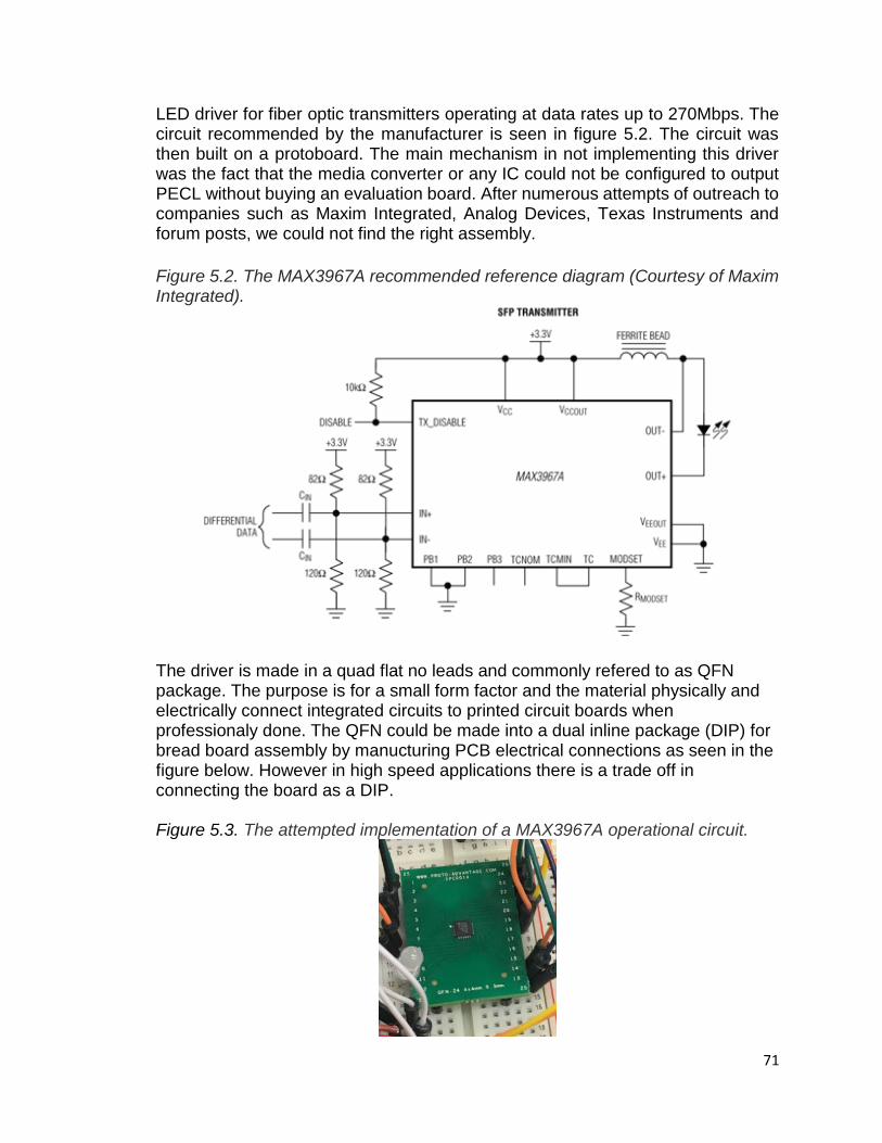
71
LED driver for fiber optic transmitters operating at data rates up to 270Mbps. The circuit recommended by the manufacturer is seen in figure 5.2. The circuit was then built on a protoboard. The main mechanism in not implementing this driver was the fact that the media converter or any IC could not be configured to output PECL without buying an evaluation board. After numerous attempts of outreach to companies such as Maxim Integrated, Analog Devices, Texas Instruments and forum posts, we could not find the right assembly.
Figure 5.2. The MAX3967A recommended reference diagram (Courtesy of Maxim Integrated).
The driver is made in a quad flat no leads and commonly refered to as QFN package. The purpose is for a small form factor and the material physically and electrically connect integrated circuits to printed circuit boards when professionaly done. The QFN could be made into a dual inline package (DIP) for bread board assembly by manucturing PCB electrical connections as seen in the figure below. However in high speed applications there is a trade off in connecting the board as a DIP. Figure 5.3. The attempted implementation of a MAX3967A operational circuit.

72
5.3.1 Laser Ethernet Transmitter Design
For the 10 Base-T laser ethernet transmitter we need to take the differential signal from an Ethernet line and drive a laser diode. The ethernet signal needs to be converted into a current which can drive the optical signal which is varied in optical intensity and can be read by a photodiode and then reamplified into the ethernet port of a computer. The operational amplifier which is mentioned before is a differential receiver. The MAX4390 provides a bias point of operation for the laser diode, and with a potentiometer RV1 we can select the current supply. The current should be able 19 mA for the laser diode we select. The TX channel supplied from the ethernet port is added to the laser diode through AC-coupling. The C23 and C7 capacitors are AC couplers and the inductors L1 and L3 isolate the frequency from the DC offset current. Then the resistors R24 and R6 set the amplitude of the laser output. The laser diode is constantly on in laser mode and can be seen by the user. The modulation swing of the signal should be about 25% of the bias point and still maintain the ability to stay above the bias point of operation.
5.3.2 Transmitter Component Layout
The third iteration was to attempt to use a laser diode as the medium of choice. A laser diode has considerable bandwidth because of the lower dispersion than an LED, low power and pin point directionality; therefore, it can still meet the goals of the project. The laser diode needs less current to drive the device so therefore different integrated circuits can be used. As mentioned earlier in chapter 2, it required analytical thinking to meet the project goals and this is the process to achieve it. Initially the transmitter was put together on NI Multisim to get a picture if the device can handle the frequency required. However, there was difficulty because the laser diode could not be modeled on the program and the Ethernet signal was not readily available for the data to test. Instead we used bipolar voltage at -2.5 V and 2.5 V at 10 MHz frequency. Given that, we were able to see that the design clearly could put out a good voltage and the current could be controlled with the potentiometer. The design can be further figured out with assembly, and it is going to be slightly easier once the PCB is assembled. The transmitter was verified to work under the frequency conditions also known as the transient response. This helps determine the maximum data throughput of the device.
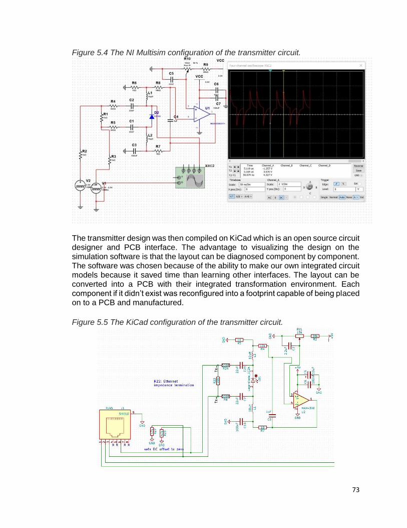
73
Figure 5.4 The NI Multisim configuration of the transmitter circuit.
The transmitter design was then compiled on KiCad which is an open source circuit designer and PCB interface. The advantage to visualizing the design on the simulation software is that the layout can be diagnosed component by component. The software was chosen because of the ability to make our own integrated circuit models because it saved time than learning other interfaces. The layout can be converted into a PCB with their integrated transformation environment. Each component if it didn’t exist was reconfigured into a footprint capable of being placed on to a PCB and manufactured.
Figure 5.5 The KiCad configuration of the transmitter circuit.
74
5.3 Receiver System Model
5.3.1 Receiver Components
The receiver system is main purpose is to convert the optical signal generated from the transmitter and drive an electrical signal into the pair of RX cables in the Ethernet jack. The design starts with a transimpedance amplifier (TIA) or differential driver OPA 695. The TIA changes the photocurrent of a reverse biased photodiode into a voltage signal with a gain resistor of 1 kΩ controlling the output. The high bias voltage of the photodiode is controlled via the MIC 2605. The DC jack on the board should be fed into the MIC 2605 where it can be translated into a voltage of 24 V for the device. After the TIA OPA 695 the signal is still weak where it needs to be amplified further. In order to convert this into a desirable signal for the Ethernet port, a comparator device LT1713 can be used. A comparator is a type of IC which provides an inverted and non-inverted output which essentially means it is going to see if a voltage is above or below a threshold level and redefine it back if it is above that threshold or make it zero if below threshold. Since Manchester encoding is square waves this will redefine out the signal properly. Since the signal is coming out as a square wave, it still would need to be defined in the proper peak-to-peak of 5V into a 100 Ω differential, however another buffer operational amplifier needs to be implemented. An IC which acts as a dual operational amplifier is used the MAX 4392. The MAX 4392 redefines the signal back into a reliable one for a RX in the Ethernet cable.
5.3.2 Receiver Layout
For U1 of the diagram OPA 695, the R1 resistor controls the current into the photodiode and the C1 is a bypass capacitor to negate the effects of the AC signal into the photodiode. Then the R10 and C24, R14 act as a current control and low pass filter respectively. The R3 is the gain controlling resistor and C3 is not connected but added to the PCB design in order to have a bit of leeway. The LT1713 operates with the same set of bypass capacitor and current controlling resistor as U1. After passing through a high pass filter in C9 and R11 the signal is ready to be compared for the IC. The R17 allows for maximum gain of the LT1713. The output coming out of this device should look like a perfect square excluding the ripple effect of the Fourier components. Lastly the MAX4392 redefines the output for termination back into the ethernet jack.
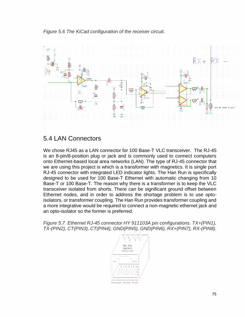
75
Figure 5.6 The KiCad configuration of the receiver circuit.
5.4 LAN Connectors We chose RJ45 as a LAN connector for 100 Base-T VLC transceiver. The RJ-45 is an 8-pin/8-position plug or jack and is commonly used to connect computers onto Ethernet-based local area networks (LAN). The type of RJ-45 connector that we are using this project is which is a transformer with magnetics. It is single port RJ-45 connector with integrated LED indicator lights. The Han Run is specifically designed to be used for 100 Base-T Ethernet with automatic changing from 10 Base-T or 100 Base-T. The reason why there is a transformer is to keep the VLC transceiver isolated from shorts. There can be significant ground offset between Ethernet nodes, and in order to address the shortage problem is to use opto-isolators, or transformer coupling. The Han Run provides transformer coupling and a more integrative would be required to connect a non-magnetic ethernet jack and an opto-isolator so the former is preferred.
Figure 5.7. Ethernet RJ-45 connector HY 911103A pin configurations. TX+(PIN1), TX-(PIN2), CT(PIN3), CT(PIN4), GND(PIN5), GND(PIN6), RX+(PIN7), RX-(PIN8).
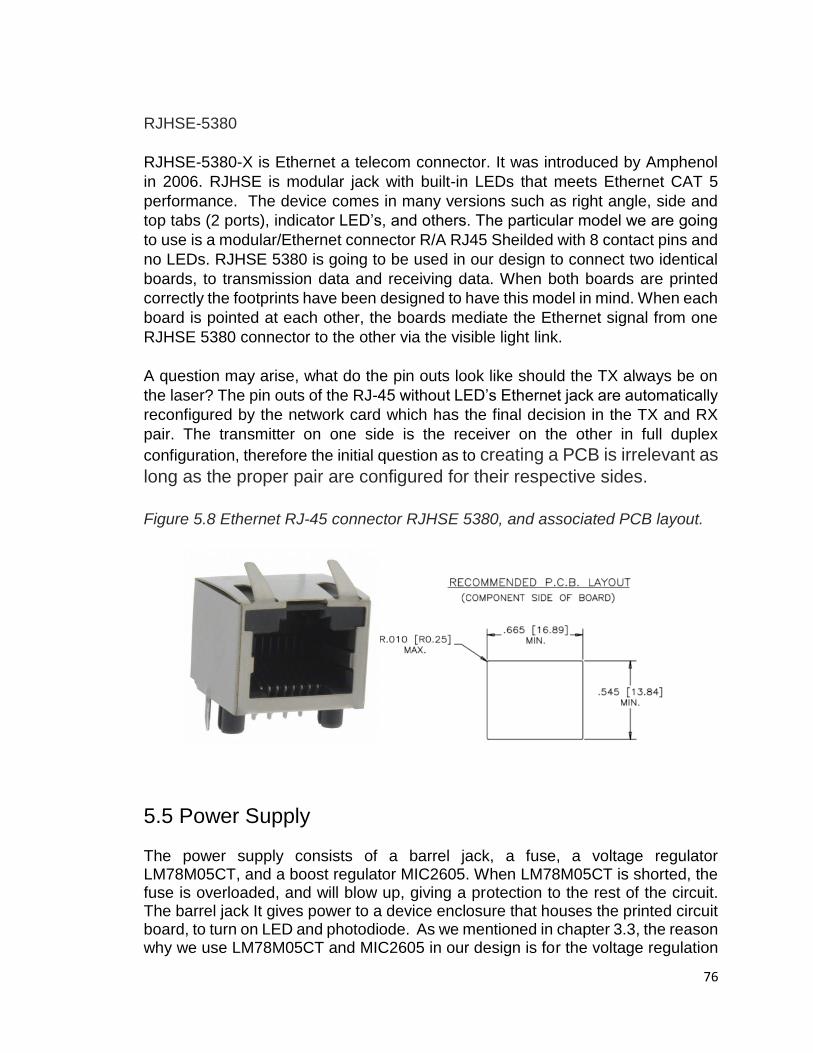
76
RJHSE-5380
RJHSE-5380-X is Ethernet a telecom connector. It was introduced by Amphenol
in 2006. RJHSE is modular jack with built-in LEDs that meets Ethernet CAT 5
performance. The device comes in many versions such as right angle, side and
top tabs (2 ports), indicator LED’s, and others. The particular model we are going
to use is a modular/Ethernet connector R/A RJ45 Sheilded with 8 contact pins and
no LEDs. RJHSE 5380 is going to be used in our design to connect two identical
boards, to transmission data and receiving data. When both boards are printed
correctly the footprints have been designed to have this model in mind. When each
board is pointed at each other, the boards mediate the Ethernet signal from one
RJHSE 5380 connector to the other via the visible light link.
A question may arise, what do the pin outs look like should the TX always be on
the laser? The pin outs of the RJ-45 without LED’s Ethernet jack are automatically
reconfigured by the network card which has the final decision in the TX and RX
pair. The transmitter on one side is the receiver on the other in full duplex
configuration, therefore the initial question as to creating a PCB is irrelevant as
long as the proper pair are configured for their respective sides.
Figure 5.8 Ethernet RJ-45 connector RJHSE 5380, and associated PCB layout.
5.5 Power Supply The power supply consists of a barrel jack, a fuse, a voltage regulator LM78M05CT, and a boost regulator MIC2605. When LM78M05CT is shorted, the fuse is overloaded, and will blow up, giving a protection to the rest of the circuit. The barrel jack It gives power to a device enclosure that houses the printed circuit board, to turn on LED and photodiode. As we mentioned in chapter 3.3, the reason why we use LM78M05CT and MIC2605 in our design is for the voltage regulation

77
and voltage reconfiguration. Now we are going to talk about what is a barrel jack and fuse. Also, we are including which one we are going to use. A Barrel jack is a coaxial power connector. It is used for low voltage device. There are many different sizes of barrel jacks. Contact ratings commonly vary from unspecified up to 5 amperes. The smaller types usually have lower current and voltage ratings. The DC Power Connector, Jack, 3A, 1.95 mm will be used in our design. A Fuse is an electrical current interrupting device that which operates to provide overcurrent protection of an electrical circuit by creating an open circuit condition in response to excessive current. In our design, the fuse is used as a conduit between an electrical power source from DC barrel jack and an electrical component. The 5X20mm 315mA Fast-Blow Fuse 250v 315mA will be used on the PCB. The power supply is regulated through a standard transformer into a barrel jack which accepts 12 V and the linear voltage regulator LM78M05CT creates a 9 V transformation for the MIC2605 to implement. The boost regulator will generate the high voltage about 30V to implement onto the photodiode. The LM78M05 has indicator LED’s to make sure the system is receiving the correct voltage. In addition, there are several rails of power created for the device. The MIC 2605 is then used to increase the voltage to the photodiode for the 30V rail. It is required that 12V DC 3A power supply with a 1.95 mm coaxial male plug be supplied in order to achieve the desired input voltage for PCB. In addition, the boost regulator MIC 2605 is not protectable by the fuse in our particular set up.
Figure 5.9 The KiCad configuration of the power supply circuit.

78
5.6 Device Housing The VLC project will be put into an enclosure to make it more professional, in its appearance, as well as its ability to resist general wear and tear. Below is a 3D rendering of our initial device enclosure design made in AutoCAD. The box itself is quite small at only 3" x 3" x 1.5" in the order of length, width, then height. The front of the box contains two holes cut out for future lens placement, the purpose of these lenses is discussed in chapter 3. The back face of the box contains a hole for the RJ45 jack to be easily connected to electronics inside the box without having to open it. The two sides are lined with vents to help keep the electronics cool while in operation. There is also a barrel jack opening for the power supply that is not shown in this rendering. Finally, there is a lid that is secured by 4 screws to keep the contents safe and locked inside. This is a preliminary design and is subject to change.
Figure 5.10 The housing complex of the laser transceiver design.
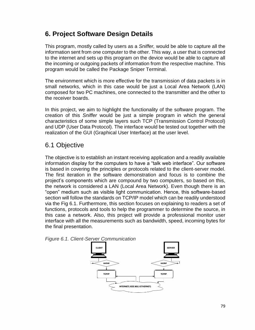
79
6. Project Software Design Details This program, mostly called by users as a Sniffer, would be able to capture all the information sent from one computer to the other. This way, a user that is connected to the internet and sets up this program on the device would be able to capture all the incoming or outgoing packets of information from the respective machine. This program would be called the Package Sniper Terminal. The environment which is more effective for the transmission of data packets is in small networks, which in this case would be just a Local Area Network (LAN) composed for two PC machines, one connected to the transmitter and the other to the receiver boards. In this project, we aim to highlight the functionality of the software program. The creation of this Sniffer would be just a simple program in which the general characteristics of some simple layers such TCP (Transmission Control Protocol) and UDP (User Data Protocol). The interface would be tested out together with the realization of the GUI (Graphical User Interface) at the user level.
6.1 Objective The objective is to establish an instant receiving application and a readily available information display for the computers to have a “talk web interface”. Our software is based in covering the principles or protocols related to the client-server model. The first iteration in the software demonstration and focus is to combine the project’s components which are compound by two computers, so based on this, the network is considered a LAN (Local Area Network). Even though there is an “open” medium such as visible light communication. Hence, this software-based section will follow the standards on TCP/IP model which can be readily understood via the Fig 6.1. Furthermore, this section focuses on explaining to readers a set of functions, protocols and tools to help the programmer to determine the source, in this case a network. Also, this project will provide a professional monitor user interface with all the measurements such as bandwidth, speed, incoming bytes for the final presentation.
Figure 6.1. Client-Server Communication

80
Interfacing with the level of transport in this system may require sockets, so this component will be a major topic to explain in the software. Socket programming is something which will take over mostly the whole part of coding part. Since in this project it is unnecessary to tediously go into the details of the programing code, the group still feels it is necessary to explain the “Pseudocode” so a reader can know how this program works. The Design of the GUI (Graphical User Interface) will be preliminary, so that any design in this section may change in the future.
6.1.1 Analysis
The development of this “Terminal” tool will be shown in phases of analysis, design and implementation. Firstly, the analysis is dedicated to the understanding and modeling of application and the domain in which it works. The initial input of the analysis phase is a description of the problem to be solved and it provides a conceptual overview of the proposed system. The output of the analysis is a formal model that captures the corresponding aspects of a networking data transmission: the verification of the link communication measurements such as bandwidth, speed, incoming and outgoing bytes and others. The requirements that were required were: Having a knowledge of the TCP/IP protocol stack. Having a knowledge on socket programming. How a Local Area Network (LAN) works. What a Client-Server software model is. Through these essential requirements, with a little help of some others attributes that will be mentioned later on, it is possible to find a good communication between two computers and obtain its measurements, so we can prove the characteristics of this type of communication through visual light.
6.1.2 Software Development
The software development on this project, from the economic and business point of view, is focused on satisfying user needs. Therefore, it could be said that the fundamental problem of the software development is how well integrated it could be in the future so the user satisfaction can be solved together with the hardware part of this project, so the whole project packet would end up in a way that through each iteration of the hardware development, the software should not require a relatively large change. The attempt to satisfy user needs could bring out new challenges since customer feedback is the driving factor of product development. This leads to the creation of a software that holds all the necessary parameters for the design. The software must meet the requirements of the TCP/IP protocols and networking standards of IEEE 802.3 Ethernet and that of the system and the user. The utilization of this software also has to be applied in limited conditions meaning without even the visible light communication medium, the software should function

81
in its scope of functionality. The reason is the scope of this software is just to show the data transmission on a LAN, in this case just two computers. Despite this, the robustness and versatility of this tool will create the ability to understand the scope of the hardware implementation.
6.1.3 Software Reutilization
Software reuse is a technological alternative to increase performance and save time. Although software reutilization may be seen for some people as not loyal, it is, in reality, an alternative to complete the specification of new applications improving the quality and productivity of the process of engineering requirements in the context of enterprise software production. An essential aspect of software reuse is the delimitation of reusable artifacts. Intuitively, reutilization is directly associated with reuse of source code to build a new software product. In this project, we make use of this alternative to improve our software’s purposes.
6.2 Program Information and Overview
The transmission of data and reception inside a multimedia device involves internally the applied knowledge of networking and protocols. Since VLC is purely hardware and following the rules of this course, we will not show any code information in this report, but we will make a quick overview in some protocol concepts which we think may highlight key aspects of the design, but may not analyze them in depth.
6.2.1 TCP/IP Protocol
This project be based on 10BASE-T Ethernet and the utilization of the packet
topology, using UTP (Unshielded Twisted Pair) cable as the physical medium to
carry information via the VLC connection. The protocol used in this software
located in the transport layer would be TCP instead of UDP mainly for its properties
it provides. To begin with, what is a protocol? A protocol is a set of formal rules for
their interaction in a computer network. The TCP protocol is located at a lower level
than the application layer and higher than Network layer following the TCP/IP stack
model. As indicated in Fig 6.2 is the hierarchical demonstration of this stack
model.14

82
Figure 6.2. The block diagram analysis of the TCP/IP stack model.
6.2.2 Network Layer
The lowest level is the network layer in which is included also the physical layer if we talked about OSI protocol stack. Network layer defines how data is physically sent through the network. For purposes of this project, we have chosen to utilize the 10Base-T Ethernet standard. The upper layer of the network protocol determines how computers send and receive the information through the physical medium. Also, we will talk about the standard connection between the MAC (Medium Access Control) and PHY (Physical Layer).
6.2.3 Internet Layer
This layer defines the way a message is transmitted through different types of networks until they reach their destination. The main protocol of this layer is the IP although there are other protocols at this level such as ARP, ICMP and IGMP. This layer provides the addressing of IP and determines the optimal route through the routers that must follow a packet from source to destination.
6.2.4 Transport Layer
The purpose of Transport layer is to permit devices on the source and destination hosts to carry on a conversation. This layer also defines the level of service and status of the connection used when transporting data. In this project we decided to make use of the TCP protocols which quite fit into the goals of this project.
6.2.5 Application Layer
Once we have established the communication from the origin to the destination, then the crux is what has been communicated over the transmission? This layer provides us with distinct Internet services such as: emails, websites, FTP, TELNET, etc. For the purpose of this project we decided to develop an FTP application to transmit a file from sender to receiver.

83
6.2.6 IP (Internet Protocol)
IP is the main protocol of Internet layer in this case. This protocol defines the basic unit of data transfer between the origin and the destination, traversing the entire network of Networks. IP can be either non-connection oriented in which all the packets may have distinct routes between origin and destination or unreliable because the packets can get lost, damaged or arrive delayed. Each computer connected to a network/internet, has at least and each connection device has a MAC address. The IP address is of type X.X.X.X and servers to distinguish one computer from another when they are connected. The MAC address is “recorded” on each connection device (network cards, routers, modems …) and in theory there should not be 2 equals in the world. Let’s see an example that will help us understand the following paragraph. For example, of our mini network, let’s assume that the IP of computer A is 1.1.1.1 and that of computer 2 is 2.2.2.2 and MAC addresses of their network cards are MAC1, MAC2 respectively.
6.3 Integrated Development Environment & Features to Develop Following IEEE 802.3 Ethernet standards for the hardware design, TCP/IP protocols for the communication from source to destination and requirements, the software part of this project will be implemented fully in Visual Studio C#, where the user-friendly web interface will have two main sections, the first one will be the Packet Generator, and the second one will be the Sniffer, which will be the one that monitors and captures the following protocols: ICMP, UDP, TCP. The purpose of the software is broken down into two main tasks: checking the speed of information from transmitter to receiver, and how accurate the information is according to the requirement of this project. Furthermore, the aforementioned protocols will be analyzed.
6.3.1 ICMP (Internet Control Message Protocol)
ICMP is a supporting protocol that allows the exchange of control and monitoring messages from end-to-end. Any anomaly detected by the IP protocol causes exchange of ICMP messages between the nodes of the network. Any anomaly in the messages could prevent the data from reaching routers or host.
6.3.2 UDP (User Datagram Protocol)
Although we won't use this protocol for the data transmission, it's good for it to to be mentioned. This protocol is non-connection oriented, and hence it does not provide any kind of error and flow control, rather it uses ways to detect errors. UDP is a very simple but there’s no handshaking between UDP sender, and receiver.

84
There is no preservation of the sequence of information provided by the application. This way, each UDP segment is handled independently of others and can blast away as fast as desired providing no congestion.
6.3.3 TCP (Transmission Control Protocol)
TCP is one of the main protocols of TCP/IP model where whereas the IP protocol deals only with packets TCP enables two host to establish a connection and exchange streams of data. TCP guarantees delivery of data and also guarantees that packets will be delivered in the same order in which they we sent unlike UDP protocol.
6.3.4 Ethernet and TCP/IP Relationship
Ethernet covers the upper layer of the Network Layers and is more related to physical medium plus some low-level elements like message collision detection. TCP/IP worries about getting a message to where it is going. TCP/IP is usually found on Ethernet, but it can be used on other networks as well. If you want to build an application based on Ethernet and TCP/IP just learn the basics of Ethernet, TCP/IP, sockets, ports, and the difference between switches and hubs, and how to ‘ping’ and address. The following figure reflects the layers for 10BASE-T Ethernet.
6.4 Software Flowchart In the Fig 6.3. This flowchart offers a visual representation of the sequence of steps and decisions needed to make the file transmission over the TCP protocol across the network. The proper application protocol used in this project was an FTP which stand which in file transmission process will work effectively and efficiently with the TCP. This flowchart also defines the inputs such as IP address, port as well as the actions executed by the client and server during the communication. The hosts in the system will be managed by the user who has full control of both ends of the software, sender and receiver. The server or receiver is the one who initiates the connection and waits for any incoming connection which in this case is the client or sender. Connections will be established between client and server, otherwise the data flow won't occur.
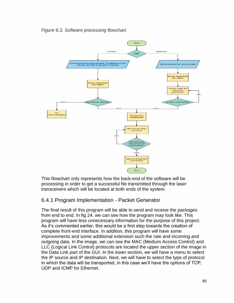
85
Figure 6.3. Software processing flowchart.
This flowchart only represents how the back-end of the software will be processing in order to get a successful file transmitted through the laser transceivers which will be located at both ends of the system.
6.4.1 Program Implementation - Packet Generator
The final result of this program will be able to send and receive the packages from end to end. In fig 24. we can see how the program may look like. This program will have less unnecessary information for the purpose of this project. As it’s commented earlier, this would be a first step towards the creation of complete front-end interface. In addition, this program will have some improvements and some additional extension such the rate and incoming and outgoing data. In the image, we can see the MAC (Medium Access Control) and LLC (Logical Link Control) protocols are located the upper section of the image in the Data Link part of the GUI. In the lower section, we will have a menu to select the IP source and IP destination. Next, we will have to select the type of protocol in which the data will be transported, in this case we’ll have the options of TCP, UDP and ICMP for Ethernet.
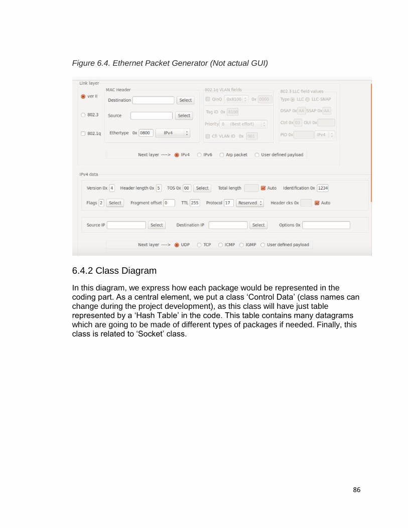
86
Figure 6.4. Ethernet Packet Generator (Not actual GUI)
6.4.2 Class Diagram
In this diagram, we express how each package would be represented in the coding part. As a central element, we put a class ‘Control Data’ (class names can change during the project development), as this class will have just table represented by a ‘Hash Table’ in the code. This table contains many datagrams which are going to be made of different types of packages if needed. Finally, this class is related to ‘Socket’ class.

87
Figure 6.5. Class Diagram representing the packet flow protocols.
6.5 Application of HTI (Human and Technology Interaction) To obtain a GUI that is easy and intuitive, we based the creation of this interface on some HTI rules. For this program, we have used the usability techniques discussed to make it clear. In this situations in which a new program is developed, the study of people, technology and the way in which they are influenced by them, then the final product can be more usable for people. But why do I use HTI techniques for the project? What benefits does using HTI bring? The use of these techniques can be thought as loss of time sometimes, but the real fact is it is that we live in technological world full of complicated devices that, in many cases, see more designed to make life difficult for us than to make it easier. In a world of instructions manuals, in which without them we can reach impossible to perform a task, such as programming a video without the manual. On a relative note for this project, in regards to software, the way to interact with this new technology may go together with some new applications as well a way to illustrate the streaming process to make this idea more vivid. Usually, we are

88
the ones who must adapt to the device we want to interact with. For this reason, the designed systems will have to be intuitive, relatable and highlight the design features.
6.6 Software Testing The software testing is necessary to verify the different elements involved in the correct used of fragments and if the protocols used are well implemented. In this project, the software has to be tested together with the hardware to check the physical medium (Unshielded Twisted Pair Ethernet Cable) used in the hardware plus other components involved on the boards. Testing a program means running it under controlled conditions which can allow to observe the outcomes of this project. The software will follow these four levels to have a good functionality:
6.6.2 Unit Testing
During this first round of testing the program is submitted to assessments that focuses on specific units or components of the software to determine whether the components of program is fully functional. The main aim of this endeavor is to determine whether the application functions as designed.
6.6.2 Integration Testing
This testing allows us the opportunity to combine all of the units within a program and test them as a group. This testing level is designed to find interface defects. This is particularly beneficial because it determines how efficiently the units are running together. Keep in mind that no matter how efficiently each unit is running, if they aren’t properly integrated, it will affect the functionality of the software program.
6.6.3 System Testing
System testing is the first level in which the complete application is tested as whole. The goal at this level is to evaluate whether the system has complied with all of the outlined requirements and to see it meets the standards.
6.6.4 Acceptance Testing
The final level, Acceptance testing (or User Acceptance Testing) is conducted to determine whether the system is ready for release. During this final phase, the user will test the system to find out whether the application meets the needs of the project. Once this process has been completed and the software has passed, the program will then be delivered to production.
6.7 GUI Interface Development
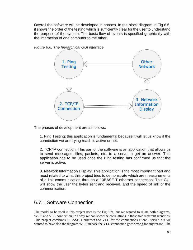
89
Overall the software will be developed in phases. In the block diagram in Fig 6.6, it shows the order of the testing which is sufficiently clear for the user to understand the purpose of the system. The basic flow of events is specified graphically with the interaction of one computer to the other.
Figure 6.6. The hierarchical GUI interface
The phases of development are as follows:
1. Ping Testing: this application is fundamental because it will let us know if the connection we are trying reach is active or not. 2. TCP/IP connection: This part of the software is an application that allows us to send messages, files, packets, etc. to a server a get an answer. This application has to be used once the Ping testing has confirmed us that the server is active. 3. Network Information Display: This application is the most important part and most related to what this project tries to demonstrate which are measurements of a link communication through a 10BASE-T ethernet connection. This GUI will show the user the bytes sent and received, and the speed of link of the communication.
6.7.1 Software Connection
The model to be used in this project uses is the Fig 6.7a, but we wanted to relate both diagrams,
Wi-Fi and VLC connection, in a way we can show the correlations in these two different scenarios.
This project combines 10BASE-T ethernet and VLC for the connections client - server, but we
wanted to have also the diagram Wi-Fi in case the VLC connection goes wrong for any reason. The

90
software is very independent of whatever network interface we want to implement to test it out, so
that is the reason why we show Wi-Fi and VLC diagrams.
Figure 6.7 The VLC (a) vs Wi-Fi (b) connection diagrams.
6.7.2 Language Selection
Since the beginning of the development of the software, it has been clear that best way to programming this tool was using Visual Studio in C# because this IDE provides a complete development toolkit for building networking applications. .NET Framework is definitely one of the best attributes in Visual Studio for network programming.

91
The user interface was proposed including the “PING” Testing to ensure the computer can “talk” to server computer, in this case the receiver board will be connected by an ethernet cable to server, here the ICMP supporting protocol is used. The basic structure of the user interface is finally developed by dividing between a not too complex TCP/IP client-server interface, in which the purpose of this is sending information or packets from client to server through the Ethernet. Originally, our thought was to create a File Transfer Protocol (FTP) or a Simple Mail Transfer Protocol (SMTP), but we opted to try just a simple client-server application that has all the necessary GUI components for a packet transferring. Finally, we created network information display which will be explained in detail later on, but the real meaning of this interface is showing the user how the network is acting during the transference of data.
6.7.3 PING Testing
Figure 6.8. The Ping testing interface.
This ping testing will send ICMP request to the destination by typing the destination's ip address or hostname. We send an ICMP echo packet to the target with the correct hostname or ip address and if this one exists, then the information of machine we tried to reach will reply, together with some metrics of that request and respond process from this application. This ping testing will also help us to be sure that the other machine is responding.
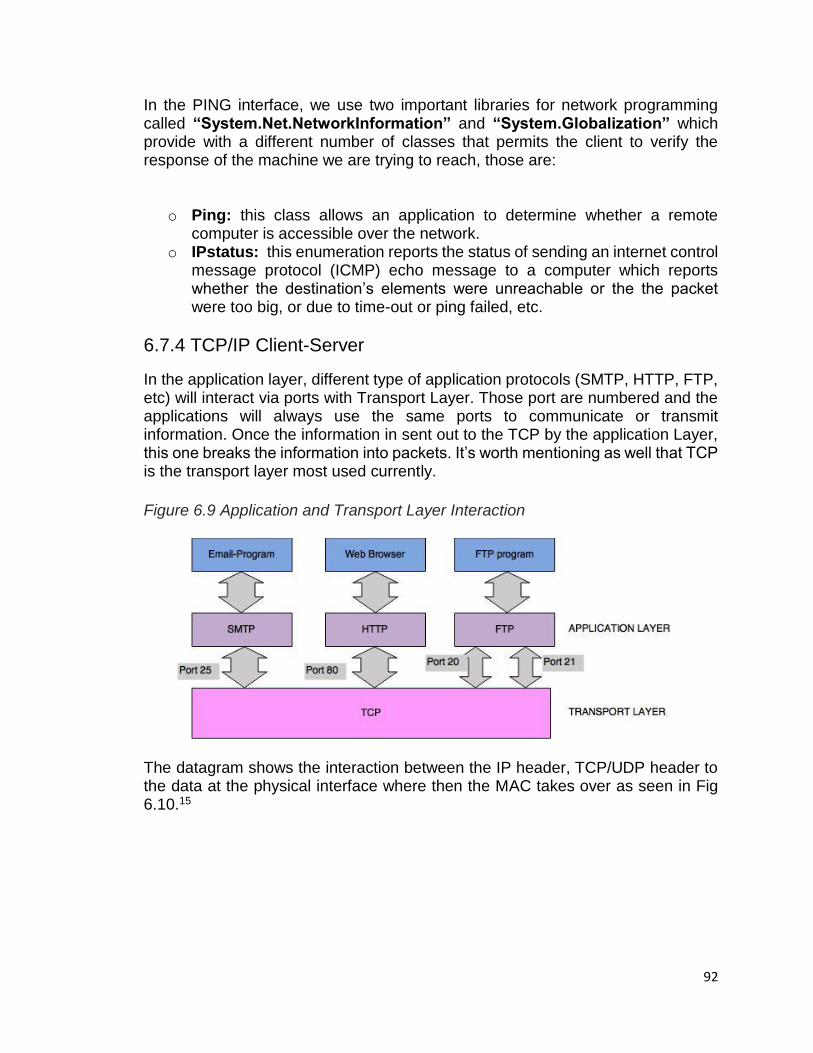
92
In the PING interface, we use two important libraries for network programming called “System.Net.NetworkInformation” and “System.Globalization” which provide with a different number of classes that permits the client to verify the response of the machine we are trying to reach, those are:
o Ping: this class allows an application to determine whether a remote computer is accessible over the network.
o IPstatus: this enumeration reports the status of sending an internet control message protocol (ICMP) echo message to a computer which reports whether the destination’s elements were unreachable or the the packet were too big, or due to time-out or ping failed, etc.
6.7.4 TCP/IP Client-Server
In the application layer, different type of application protocols (SMTP, HTTP, FTP, etc) will interact via ports with Transport Layer. Those port are numbered and the applications will always use the same ports to communicate or transmit information. Once the information in sent out to the TCP by the application Layer, this one breaks the information into packets. It’s worth mentioning as well that TCP is the transport layer most used currently.
Figure 6.9 Application and Transport Layer Interaction
The datagram shows the interaction between the IP header, TCP/UDP header to the data at the physical interface where then the MAC takes over as seen in Fig 6.10.15

93
Figure 6.10. The Datagram structures.
In the transport layer, the header contains number of control information such as, local port, remote port, a sequence number which used by the TCP, and a checksum which is a technique to calculate if the data being transmitted arrived intact or not. This TCP header has between 20 to 24 bytes of longitude. Moreover, in the Internet Protocol, the IP header is the one that receives the information from the transport layer. IP datagram uses at most 65,535 bytes including the header which may take between 20 to 24 bytes.
Figure 6.11. TCP/IP and Ethernet Layers
The datagrams generated in the Internet Layers would be transferred to the Network Interface. This Interface is defined by a type of physical network which is
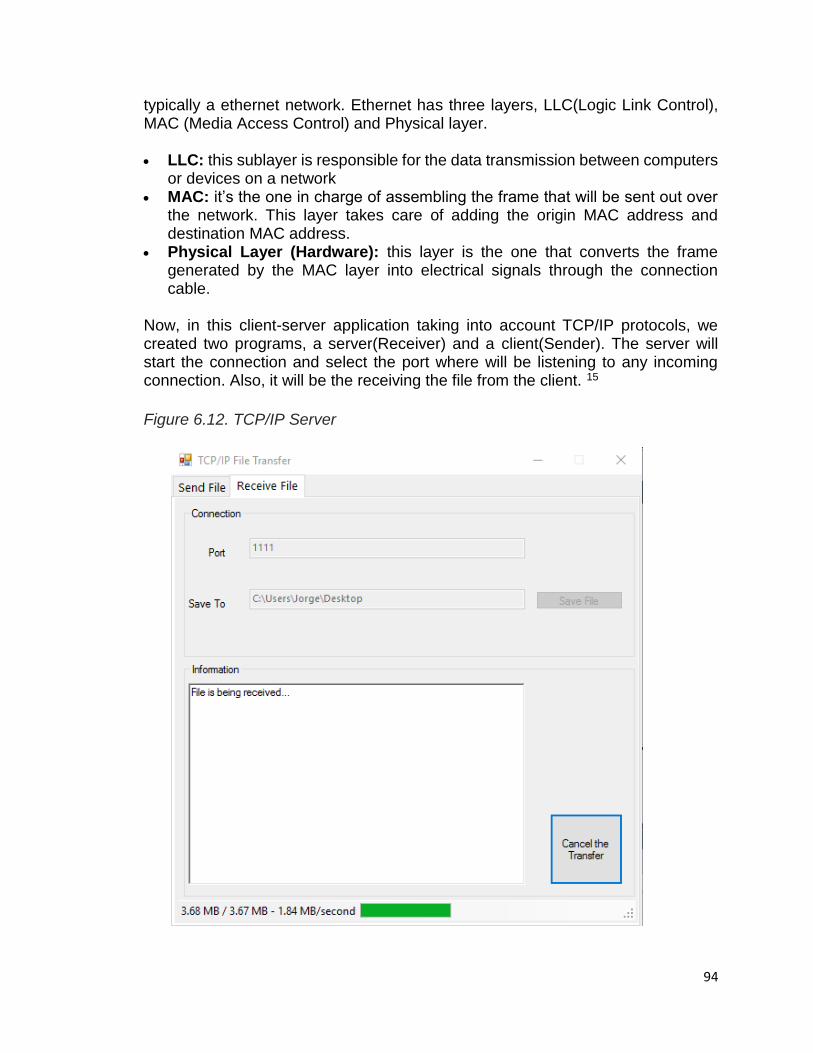
94
typically a ethernet network. Ethernet has three layers, LLC(Logic Link Control), MAC (Media Access Control) and Physical layer.
LLC: this sublayer is responsible for the data transmission between computers
or devices on a network MAC: it’s the one in charge of assembling the frame that will be sent out over
the network. This layer takes care of adding the origin MAC address and destination MAC address.
Physical Layer (Hardware): this layer is the one that converts the frame generated by the MAC layer into electrical signals through the connection cable.
Now, in this client-server application taking into account TCP/IP protocols, we created two programs, a server(Receiver) and a client(Sender). The server will start the connection and select the port where will be listening to any incoming connection. Also, it will be the receiving the file from the client. 15
Figure 6.12. TCP/IP Server

95
The fundamental purpose of Server Interface is to start a connection with the client and receiving the file being transferred by the client. The functional steps to follow to make the connection happen properly are typing the port number and selecting the location where the file will be saved. Once the previous steps are done, then the “Start Connection” button is pushed, so we instantiate the server. Once the connection is established, and server accepts the incoming file from the client, the progress bar will be tracking the progress and displaying the speed rate. In addition, the server also has the ability to cancel the file transfer at any moment during the transmission.
Figure 6.13. TCP/IP Client
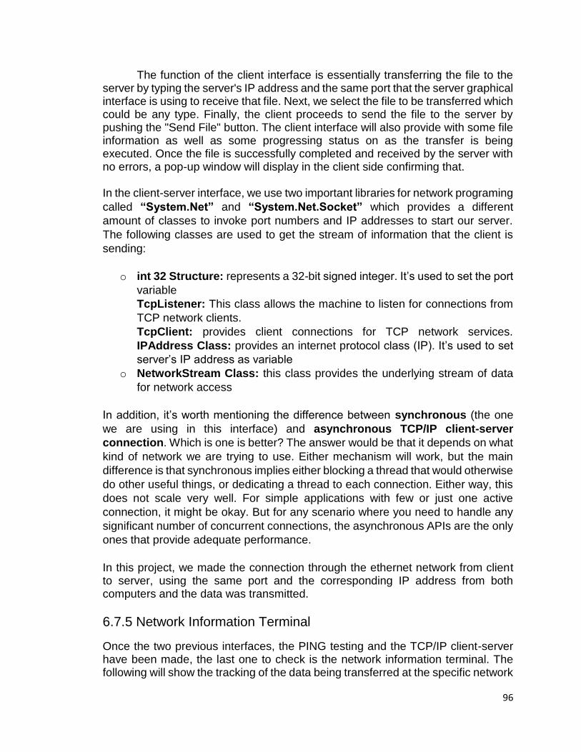
96
The function of the client interface is essentially transferring the file to the server by typing the server's IP address and the same port that the server graphical interface is using to receive that file. Next, we select the file to be transferred which could be any type. Finally, the client proceeds to send the file to the server by pushing the "Send File" button. The client interface will also provide with some file information as well as some progressing status on as the transfer is being executed. Once the file is successfully completed and received by the server with no errors, a pop-up window will display in the client side confirming that.
In the client-server interface, we use two important libraries for network programing
called “System.Net” and “System.Net.Socket” which provides a different
amount of classes to invoke port numbers and IP addresses to start our server.
The following classes are used to get the stream of information that the client is
sending:
o int 32 Structure: represents a 32-bit signed integer. It’s used to set the port
variable
TcpListener: This class allows the machine to listen for connections from
TCP network clients.
TcpClient: provides client connections for TCP network services.
IPAddress Class: provides an internet protocol class (IP). It’s used to set
server’s IP address as variable
o NetworkStream Class: this class provides the underlying stream of data
for network access
In addition, it’s worth mentioning the difference between synchronous (the one
we are using in this interface) and asynchronous TCP/IP client-server
connection. Which is one is better? The answer would be that it depends on what
kind of network we are trying to use. Either mechanism will work, but the main
difference is that synchronous implies either blocking a thread that would otherwise
do other useful things, or dedicating a thread to each connection. Either way, this
does not scale very well. For simple applications with few or just one active
connection, it might be okay. But for any scenario where you need to handle any
significant number of concurrent connections, the asynchronous APIs are the only
ones that provide adequate performance.
In this project, we made the connection through the ethernet network from client to server, using the same port and the corresponding IP address from both computers and the data was transmitted.
6.7.5 Network Information Terminal
Once the two previous interfaces, the PING testing and the TCP/IP client-server have been made, the last one to check is the network information terminal. The following will show the tracking of the data being transferred at the specific network
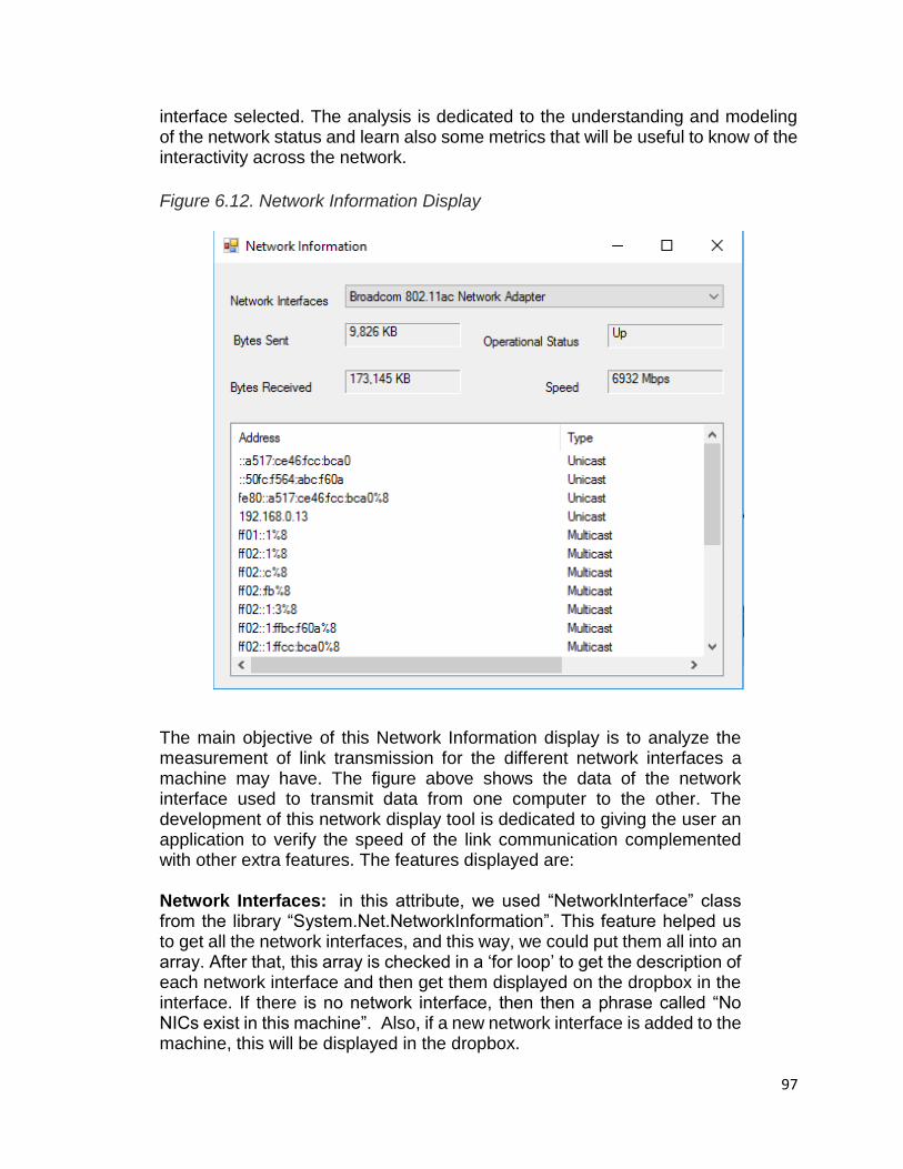
97
interface selected. The analysis is dedicated to the understanding and modeling of the network status and learn also some metrics that will be useful to know of the interactivity across the network.
Figure 6.12. Network Information Display
The main objective of this Network Information display is to analyze the measurement of link transmission for the different network interfaces a machine may have. The figure above shows the data of the network interface used to transmit data from one computer to the other. The development of this network display tool is dedicated to giving the user an application to verify the speed of the link communication complemented with other extra features. The features displayed are: Network Interfaces: in this attribute, we used “NetworkInterface” class from the library “System.Net.NetworkInformation”. This feature helped us to get all the network interfaces, and this way, we could put them all into an array. After that, this array is checked in a ‘for loop’ to get the description of each network interface and then get them displayed on the dropbox in the interface. If there is no network interface, then then a phrase called “No NICs exist in this machine”. Also, if a new network interface is added to the machine, this will be displayed in the dropbox.
98
Bytes Sent: This attribute measures the amount of data being sent from one machine to other. In this part, we used the method “BytesSent” from the library “System.Net” which gets the number of bytes that were received on the interface. The total amount of bytes received is then converted to Megabytes (KB ) by dividing it by 1024. Bytes Received: This attribute measures the amount of data being sent from one machine to other. In this part, we used the method “BytesReceived” from the library “System.Net” which gets the number of bytes that were sent on the interface. The total amount of bytes sent is then converted to Megabytes (KB ) by dividing it by 1024. Operational Status: This attribute measure the current operational state of the network interface connection. In this part, we used an ‘Enumeration’ named “OperationalStatus” which will return the following type of values: Up: The network interface is up; it can transmit data packets Down: The network interface is unable to transmit data packets. This enumeration is found in the library “System.Net.NetworkInformation” Speed: This attribute measures the speed of the current network interface. In this part we used the property “Speed” from the library “System.Net.NetworkInformation” In the ‘Rich Box’, information about the NICs on that current network interface are displayed in either IPv4 or IPv6, which are explained in the IP section. Also, the address type is displayed in the right column which indicates if the IP address is multicast, unicast or anycast. Multicast: Multicast is a communication between a single sender and multiple receivers on a network. This type of address is displayed due to a class named “MulticastIPAddressInformationCollection” located in the “System.Net.NetworkInformation” library. Unicast: Unicast is a communication between a single sender and a single receiver over a network. This type of address is displayed due to a class named “UnicastIPAddressInformationCollection” located in the “System.Net.NetworkInformation” library. Anycast: Anycast is a communication between a single sender and the nearest of several receivers in a group. The term exists in contradistinction to multicast, and unicast. This type of address is displayed due to a class named “IPAddressInformationCollection” located in the “System.Net.NetworkInformation” library. 16
99
6.8 General Software Conclusion
The evaluation of the efficiency and operational quality of this software has been established under the criteria of the system and the characteristics of the type network interface used. In the development of this software, the reutilization of software source was an alternative that favors the debugging and coding of the GUI during the implementation process. During the designing, we used some protocols and standards for a better understanding of the software. The comparison between the ISO and TCP/IP model for the communication in a LAN helped to visualize the concept of what this software was trying to implement. The importance of the integration and manipulation of the TCP/IP model in this design were fundamental. The structure of this software was divided into three stages: “PING” testing, TCP/IP client-server connection, and Network Information Display
1. The first stage, The PING testing interface was developed to verify in the machine we are trying to connect with is responding. The information that this interface would generate is really important to determine if the server is active.
2. The second stage, The TCP/IP client-server interface, linked to the transport layer, assures the information gets a valid port and IP address.
3. The third stage, the Network information display checks the network interface connection which belongs basically to the network layer in the TCP/IP model. Also, it will check some other extra features such as the connection speed, network status, etc.
The problems in the software were present in Application Layer, which due to the large of data that had to be sent from client to server, the implementation of some additional plugins on interface and modifications in the code were needed unleashing out new ways to implement the IP addresses and ports in the network interface. In this chapter, we also talked about Human and Technology Interaction (HTI) which shows how the front-end implementation has to be structured in order the user can easily understand the design of the GUI. These HTI tests were applied to make the system more intuitive and readable for users.

100
7. Physical Testing and Prototype Construction
7.1 Testing Conditions The first step in constructing a prototype is to test individual components, then to test connecting components, and finally the system as a whole. There is a learning curve associated with integrated circuit semiconductor implementations. The reason being is that the relative size and form of the integrated circuits can be hard to see their individual details, therefore careful placement onto breakout boards from the company proto-advantage.com was sought. Even though their DIP packages can be easily realized, there are several physical faults which can limit the performance. The sockets that are used in a breadboard might have different permittivity thus causing reflection, and absorption of the flowing electronics, reducing the output power and changing the phase. The resolving of mismatch of impedances at high frequency is paramount to transmission of signal. Equipment: In the Senior Design lab, there is a variety of hardware made available for students to test equipment. For this project, we used the following.
Agilent E3630A Triple Output DC Power Supply
Tektronix AFG 3022 Dual Channel Arbitrary Function Generator, 25 MHz
Tektronix DMM 4050 6 ½ Digit Precision Multi-meter
Tektronix MSO 4034B Digital Mixed Signal Oscilloscope, 350 MHz, 4 Channel
CSI2205D Micro Control unit DMM auto-ranging Multi-meter Procedure: The same method(s) was followed to test each component individually, as well as each side of the transceiver and finally the system as a whole.
1. Setup breadboard by connecting all of the grounding rails to one another, and repeat for the power supply rails.
2. Place the components on the breadboard, making sure to leave enough space for passive component placement, as well as jumper wires.
3. Place passive components according to manufacturer spec sheets and the mode of operation for each IC.
4. Double check the circuit to make sure all connections are correct, there are no shorted elements, and no open circuits.
5. Place wires to act as leads for hardware i.e. two wires for input signal, two wires at each output for the oscilloscope, an additional wire at each supply voltage pin to be measured by the multi-meter.
6. Connect the power supply leads from the Agilent power supply to the terminals of the breadboard.
7. Connect the leads from the function generator to the inputs of the differential receiver.
8. Turn everything on I.e. the power supply, the function generator, the oscilloscope, and multi-meter.

101
9. Set the function generator to an appropriate signal, and tune the oscilloscope to an accommodating resolution.
10. With everything running check each input with the multi-meter to confirm that proper supply voltage is reaching each component.
11. Check the output of each component to make sure there is sufficient voltage being provided from each IC.
12. Finally using the oscilloscope leads, check and record the signal going into each IC and coming out of each IC.
Results: Using the aforementioned procedure(s) we were able to test all of the parts we ordered as well as the system as a whole. We found that the VLC system performs well with a 10 kHz differential input, where the waveform is square. We tested the same wave at 100 kHz and the system resolution was poor. We then used the function generator to produce a modulated signal of the AM variety with a carrier of 1 MHz and the modulation frequency of 10 kHz. The system resolved this signal fairly well, the same signal was used with a sine wave instead of a square and the system resolved that one well too. A detailed account is given below.
7.2 Transmitter Components In the second iteration of design, which will have a more thorough documentation, we implemented a 10-BaseT VLC transceiver. Included in the transmitter components are the differential receiver, the LED, as well as a voltage converter. The figure below shows the circuit diagram for the transmitter setup. It was created using EasyEDA, a website specializing in online circuit and PCB design. The capacitor values that you see were given by the manufacturers on the data sheet. The AD8130 has been configured for a basic gain circuit, where the gain is equal to the input voltage times 1 plus the ratio between the resistors across pins 6 and 5. In a perfect scenario this setup would produce a single signal at 4x the input voltage. The IC7660s has been configured as a simple voltage converter (Vo = -Vin). When attempting to use the AD8130, the IC needed to be converted into DIP version with an external vendor. Although there were recommendations that this would be able to hand the frequency we needed to use, when scrutinized on the lab bench, the component was not meeting the requirements.
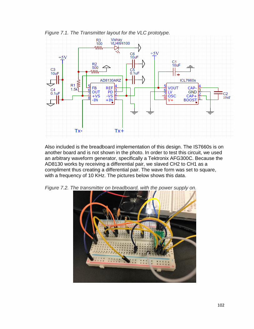
102
Figure 7.1. The Transmitter layout for the VLC prototype.
Also included is the breadboard implementation of this design. The IS7660s is on another board and is not shown in the photo. In order to test this circuit, we used an arbitrary waveform generator, specifically a Tektronix AFG300C. Because the AD8130 works by receiving a differential pair, we slaved CH2 to CH1 as a compliment thus creating a differential pair. The wave form was set to square, with a frequency of 10 KHz. The pictures below shows this data.
Figure 7.2. The transmitter on breadboard, with the power supply on.
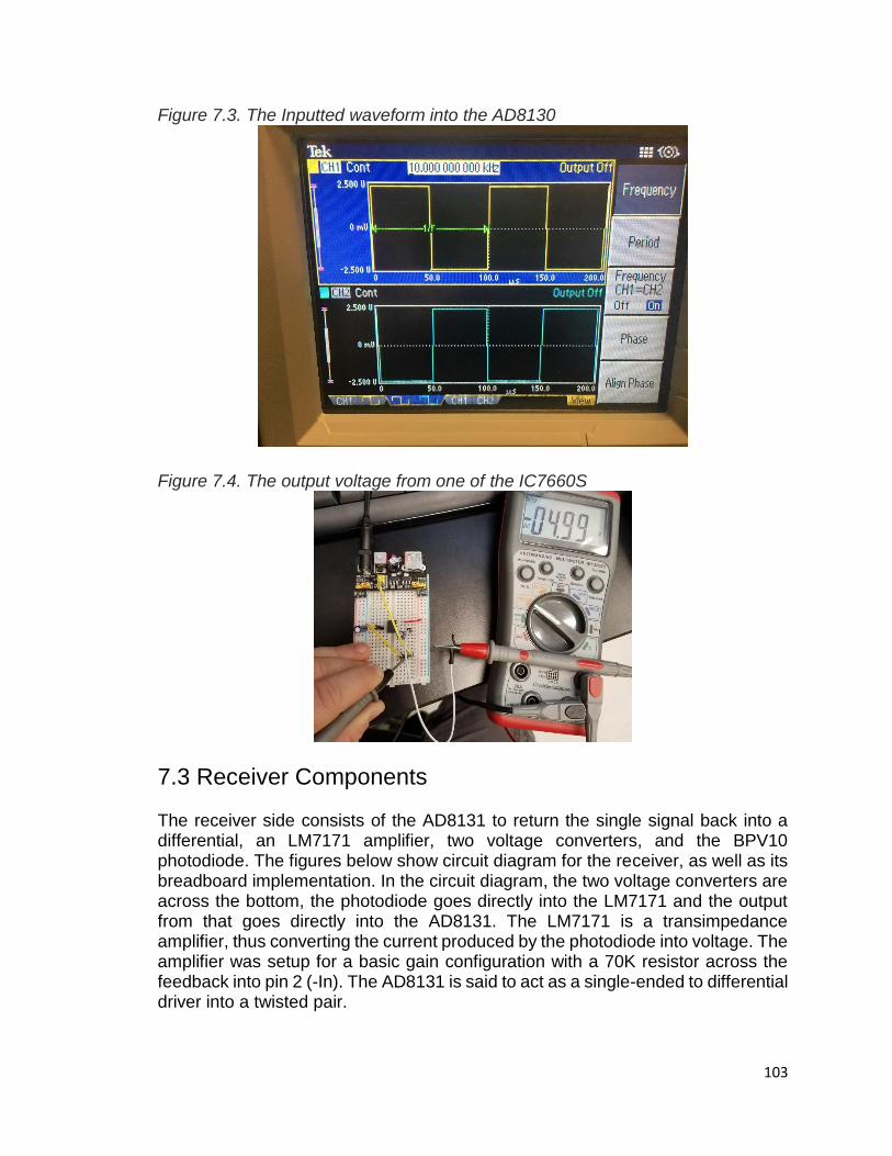
103
Figure 7.3. The Inputted waveform into the AD8130
Figure 7.4. The output voltage from one of the IC7660S
7.3 Receiver Components The receiver side consists of the AD8131 to return the single signal back into a differential, an LM7171 amplifier, two voltage converters, and the BPV10 photodiode. The figures below show circuit diagram for the receiver, as well as its breadboard implementation. In the circuit diagram, the two voltage converters are across the bottom, the photodiode goes directly into the LM7171 and the output from that goes directly into the AD8131. The LM7171 is a transimpedance amplifier, thus converting the current produced by the photodiode into voltage. The amplifier was setup for a basic gain configuration with a 70K resistor across the feedback into pin 2 (-In). The AD8131 is said to act as a single-ended to differential driver into a twisted pair.
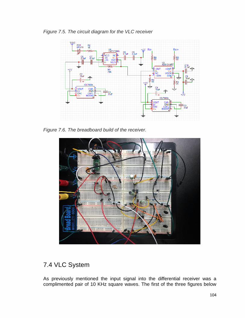
104
Figure 7.5. The circuit diagram for the VLC receiver
Figure 7.6. The breadboard build of the receiver.
7.4 VLC System As previously mentioned the input signal into the differential receiver was a complimented pair of 10 KHz square waves. The first of the three figures below

105
Fig 7.7, shows the relationship between the LED and the photodiode. The purple reading shows the signal going into the LED, the blue reading shows the signal coming out of the photodiode, being amplified and going into the AD8131. We can see that the combined differential square wave that is driving the LED maintains its shape. The second figure Fig 7.8 shows two readings, one for each of the differential outputs. The signal is recreated quite well, and is still in differential format. The third figure in this section also shows the output from the AD8131, however this time the signal going into the receiver is a differential sine wave. While it’s not exactly the input it is a reconstruction of the differential signal, and it does maintain the appropriate frequency.
Figure 7.7. The top signal coming from the photodiode, and the bottom signal coming from the LED.
Figure 7.8. The output from the AD8131 after being captured by the photodiode. The input here is a square wave, the output is also square in nature.
Figure 7.9. The output from the AD8131 after being captured by the photodiode. The input here is a sine wave.

106
When attempting to document the 100 KHz frequency and higher the resolution of the signal was degraded. There was essentially noise and we could not diagnose the error. Therefore, there was a turn into the main focus of the project as seen in chapter 5. If there was more time in completing our focus on VLC, we could use different circuit elements in the design and work with experts in high frequency electronics. One such recommendation was from Ethan Png who had recommended the design of a “Ethernet over Light” project which showed promising aspects of transmitting the 31.25 MHz signal required for 100 Base-T transmissions as seen in figure 7.1017.
Figure 7.10 Simulated transmitter (top) and receiver (bottom) signals for the 100 Base-T Ethernet over light transmission.

107
8. Project Construction
After physically testing each individual component, testing the transmitter and receiver, and testing the system as whole, the next stage of product development was to focus on designing a printed circuit board. The most important parts of this step include figuring out which company to purchase the PCB from, as well as how we will mount the components we have selected. The next chapter will give an overview of the techniques and the ancillary material includes a detailed list of parts selected, and purchased.
8.1 Printed Circuit Boards A printed circuit board or PCB is essentially a board that connects electronic components by micron size electrical wires. It is a component made of one or more layers of insulating material with electronic conductors. The insulator is typically made on the base of fiber reinforced resins, ceramics, plastic, or some other dielectric materials. It can be used for everyday electronic products where form factor is necessary and experimental prototyping is finished i.e. PCB offers many benefits such as it can be very small in size. Moreover, the printed circuit board reduces the need of assembling wires, and in turn improves the appearance of the final product while creating high reliability. There are many different types of PCB which includes single sided PCB, double sided PCB, Multilayer PCB, Rigid PCB, flex PCB, and rigid-flex PCB. Single sided PCB is the most simple and basic PCB. The components are on one side and conducting wires are on the other side. It has only on layer of conductive material. Double sided PCB is very similar to single sided PCB however, both sides of board contains electronic components and conductive layer. It is the most popular type of PCB in today’s industry. It allows traces across and under each wire, increasing density without point to point soldering. Multilayer PCBs as name implied have multiple layers and has a higher density, it includes a layer on top of double sided PCB, which makes it very thick and a high compound design. The price of multilayer PCB is relatively high. Rigid printed circuit boards use a solid, rigid substrate material like fiberglass that deters the board from twisting. Flexible PCBs consist of conductive strips of metal, usually copper, encapsulated with an insulating dielectric material made of polyimide or a solder mask. The benefit of flexible PCB is that it will reduce size and weight and maintain ruggedness. Rigid-flex PCBs combine the advantage of rigid PCBs and flexible PCBs. The circuit includes two or more conductive layers that comprise either flexible or rigid insulation material between each one - the outer layers may have either exposed pads or covers. In our design, we are going to use double sided PCB rigid PCB.

108
The design and implementation of our own PCB, is a requirement for electrical engineers in to complete the senior design, however, we had no experience with PCB design. It was a learning experience to design a PCB on our own. In today’s market, there are many different software’s available for students to design printed circuit boards for free. One of very good and easy to use software package available to our group was KiCad. The reason why we chose it is because it contains a schematic editor, parts can be placed on many sheets and connected together through ports, and the layout editor allows back annotation to the schematic and auto-routing to automatically connect traces based on the connections defined in the schematic. Also, it offers a full suite of options such as part creation, as well as direct connections to the company’s electrical component database. After we designed our own circuit on the PCB reconfiguration software, now we were ready to manufacture an actual PCB. Normally, it is hard for us to manufacture complicated printed circuits onto substrate materials therefore need to send to a professional PCB manufacture company. There are many company out there for us to choose. There are three constraints that we need to keep in mind while manufacture PCB. First constraint we have is the economic constraint, we want to keep the budget under $300. The second constraint we have is the time constraint, we need to consider how long does it take for manufacture to build PCB and send back to us. Third constraint we have is the minimum order of PCB that we need to order. The company that has been considered are list below OSH Park OSH Park is a community printed circuit board (PCB) order. It is located in the
United States. It is an aggregation service that panelizes a number of customer
orders into a single panel, then sends them out for fabrication. Standard prices are
2-layer PCBs are $5 per square inch, FR4, ENIG finish, 0.063 thickness, 1 oz.
copper, 6/6 spacing, 13/7 drills. The requirement is an order of 3 boards. If we
decided to go with a 4-layer board instead it would also include three copies of our
board but the price would double to $10 per square inch and the manufacturing
process and shipping would take a little longer as well. The price for 2 layers is
fairly low that is affordable for students. They are also a favorite of many open-
source hobbyists which will allow the design to be easily shared with others.
Design rule for Oshpark
At least 6 mil minimum trace width
At least 6 mil minimums spacing between traces
At least 15 mils of clearance from the traces to the edge of the PCB.
Hole size must be at least 13 mils
Annular rings must be at least 7 mils

109
4PCB
4PCB has student programs for college student in that it offers a very cheap and
quick delivery method for when you need your PCB right away. It costs $33 per
board which is competitive but not sufficient. A 2-layer full spec printed circuit board
would cost 33 dollars and 4-layer full spec would could around 66 dollars. There
is no minimum order requirement for this company. Also, it offers a free design tool
“PCB Artist” that can be used to develop the design needed. 4PCB offers a free
file review which is reviewed by engineers so if there are any errors in design they
will be found immediately with no surprises later. This company has very good
reviews in respects to quality and cost. However, we need two boards and can get
more for almost the same price from OSH Park. Express PCB As the name implies, express PCB offers a very fast service, and the time is guaranteed to be 2 days in delivery. The cost of the PCB is a little bit higher than other company, it is at 51 dollars for a 2-layer and 99 dollars for a 5 layer. The shipping charged is 10 dollars for its express shipping. This would be a great option when time is very limited. PCB-pool
PCB-pool is another company that offer no minimum order, it has multiple locations
throughout the world. It has many software choices such as eagle cad, PCAB. The
price is a bit higher than 4PCB at 42 dollars for 2-layer and 100 dollars for 4-layer
full spec printed circuit boards. The company is located in Germany, which causes
a problem, mainly shipping. The international shipping will increase the cost and
time of delivery for our PCB design. Even though it has very good reviews, but it
is better to order form the United States. PCB4Less PCB4Less is a relatively cheap manufacturer, as name mentions. PCB4Less offers a complete line of printed circuit board fabrication with cutting-edge technology and guaranteed ability to deliver. The price for the PCB of 2 layers $19 and 4 layers for $39. There is no minimum order required. And the time takes it delivery is about 5 to 7 days.
110
Below is the table to compare different PCB Manufacture Company.
Company Min. order Time Cost Website
Oshpark 3 5 days $36 https://oshpark.com
4PCB 1 5 days $33 http://www.4pcb.com/
Express PCB
1 2 days $51 https://www.expresspcb.com/
PCB-pool 1 8 days $42 http://www.pcb-pool.com/
PCB4less 1 5-7 days $19 http://www.pcb4less.com/
After comparing and contrasting the aforementioned printed circuit board
manufacturers and weighing their advantage and disadvantage we collectively
decided to order PCB from OSH Park. We used OSH Park for our manufacturer
company due to its low cost and fast delivery and multiple delivery order for a low
price. The reason 4PCB is not used is because it comparatively more expensive
than OSH Park as from table above, Obliviously, the PCB-pool will not be used
due to high price, and long shipping. Express PCB offer very fast shipping;
however, the price is not a good choice, and we are not rush at this moment.
PCB4less does not have as good review as OSH Park, and it takes longer time to
delivery. The most important thing that will add flexibility to choices in PCB
manufacturers will be how much time we can spare. As such, we will need to begin
designing the schematic and PCB as soon as possible to take advantage of these
options. Otherwise, the rush processing can get very expensive. A good news is
by now, we have gotten 5 orders of laser ethernet transceiver board from OSH
Park for 12 dollars a board.
8.2 Soldering
The general techniques that can be used to mount an electrical component to a printed circuit board are general soldering of the component, through-hole soldering, and surface mounting technology. Surface mounting technology is more popular nowadays because of demanding for smaller weight and size of packaging. We usef all three soldering techniques to solder the components on the LET board ourselves.
Surface mount technology Surface mount technology is the process by which components are mounted directly onto the surface of the PCB. Surface mount technology components either have smaller leads, or no leads at all which could reduce the resistance and inductance. Surface mount technology component is generally smaller than

111
through-hole soldering. Because of surface mount technology on PCB does not require as many drilled holes, and the components are more compact, higher circuit densities are possible on smaller boards. This is reason why today’s technologies are getting smaller and smaller. One advantage of surface mount technology is that it is generally less expensive than through-hole components. They are often offer a better level of performance and they can be used with automated pick and place machine that in many cases all but eliminates the need for manual intervention in the assembly process which will reduced the cost of product. However, there is one disadvantage of surface mount technology which is the construction is not suitable when there are requirements for high power or large high-voltage parts such as in high power circuits.
Through-hole soldering
Through-hole mounting is the process by which component leads are placed into drilled holes on a bare PCB. The process was standard practice until the rise of surface mount technology (SMT) in the 1980s, at which time it was expected to completely phase out through-hole. One advantage of through-hole mounting is it is extremely reliable, as it provides strong mechanical bonds. However, there are many disadvantages of through-hole mounting compared to surface mounting which include the additional drilling makes the production of boards significantly more expensive and less dense in components. Additionally, the presence of holes in the PCB creates limitations in terms of the available routing area for signal traces on the layers which are immediately beneath the top layer on multi-layer boards. While a surface mount literally affixes the component to the top surface of the board, a through-hole attaches the component to the board by providing holes in the board to allow the component lead to go through the board and exit the opposite side of the board. General soldering General soldering connects electrical wiring and electronic components to printed circuit boards. It is a process in which two or more metal items are joined together by melting and then flowing a filler metal into the joint. The metal to be soldered is heated with a soldering iron and then solder is melted into the connection Surfaced mount technology and through-hole mounting are two types of soldering are popular in today's market. However, in our project, we are going to soldering the components on BS board our self by using all three techniques. We will need a hot air gun during the soldering. We are going to do this PCB with ordinary soldering iron. The footprint on the PCB is deigned to make soldering easily for us. Since we have no experience on soldering electronic components before, here are some general tip to know before we soldering.

112
a. First of all, we need to clean all components, tools, and to be used in the soldering process.
b. Then we need to choose an alloy which is lead-tin. Usually we use 40% of lead, and 60% of tin.
c. Adjust a soldering iron to appropriate temperature, d. Select the right flux, flux is an agent that prevents oxidation and removes
the thin layer of oxide. e. Then we need a clamp to hold electronic components, which is usually very
small. f. Select the right electronic component and double check which pins are
which and make sure with no mistakes. g. Soldering on the PCB, hold the soldering iron and heat both the lead and
the pad simultaneously. Touch the solder wire in the space between the iron tip and the lead, Keep the soldering iron tip still while moving the solder around the joint as it melts. Allow to the joint to cool naturally and undisturbed, do not blow on the solder joint to cool it.
h. Good soldering joint: will be shiny and concave in nature, will be clean and free of dirt, and will fully cover the pad component lead lays and passing through.
8.3 PCB assembly Firstly, designing the PCB on KiCad required several layer topologies to be able to work such as the copper, silk, adhesives, drill holes. For the most part, they were easily redone with a functionality in the software which allowed for the viewing of the traced schematic onto the PCB. After watching some tutorials of moving wires and realigning parts, we have managed to come up with the following printed circuit board.
Figure 8.1 The KiCad Configuration of the Laser Ethernet Transceiver Circuit
Board.
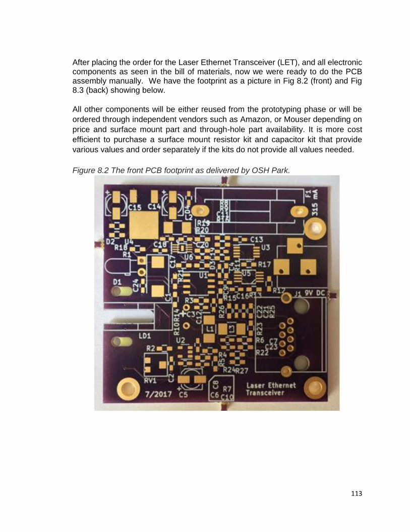
113
After placing the order for the Laser Ethernet Transceiver (LET), and all electronic components as seen in the bill of materials, now we were ready to do the PCB assembly manually. We have the footprint as a picture in Fig 8.2 (front) and Fig 8.3 (back) showing below.
All other components will be either reused from the prototyping phase or will be
ordered through independent vendors such as Amazon, or Mouser depending on
price and surface mount part and through-hole part availability. It is more cost
efficient to purchase a surface mount resistor kit and capacitor kit that provide
various values and order separately if the kits do not provide all values needed.
Figure 8.2 The front PCB footprint as delivered by OSH Park.
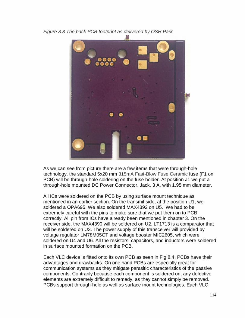
114
Figure 8.3 The back PCB footprint as delivered by OSH Park
As we can see from picture there are a few items that were through-hole technology. the standard 5x20 mm 315mA Fast-Blow Fuse Ceramic fuse (F1 on PCB) will be through-hole soldering on the fuse holder. At position J1 we put a through-hole mounted DC Power Connector, Jack, 3 A, with 1.95 mm diameter. All ICs were soldered on the PCB by using surface mount technique as mentioned in an earlier section. On the transmit side, at the position U1, we soldered a OPA695. We also soldered MAX4392 on U5. We had to be extremely careful with the pins to make sure that we put them on to PCB correctly. All pin from ICs have already been mentioned in chapter 3. On the receiver side, the MAX4390 will be soldered on U2. LT1713 is a comparator that will be soldered on U3. The power supply of this transceiver will provided by voltage regulator LM78M05CT and voltage booster MIC2605, which were soldered on U4 and U6. All the resistors, capacitors, and inductors were soldered in surface mounted formation on the PCB. Each VLC device is fitted onto its own PCB as seen in Fig 8.4. PCBs have their advantages and drawbacks. On one hand PCBs are especially great for communication systems as they mitigate parasitic characteristics of the passive components. Contrarily because each component is soldered on, any defective elements are extremely difficult to remedy, as they cannot simply be removed. PCBs support through-hole as well as surface mount technologies. Each VLC
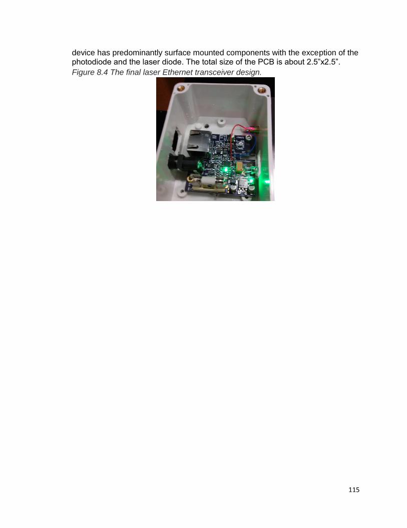
115
device has predominantly surface mounted components with the exception of the photodiode and the laser diode. The total size of the PCB is about 2.5”x2.5”.
Figure 8.4 The final laser Ethernet transceiver design.
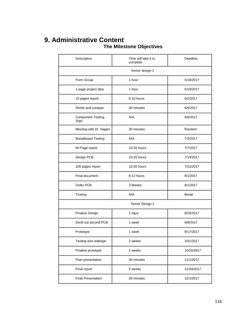
116
9. Administrative Content The Milestone Objectives
Description Time will take it to complete
Deadline
Senior design 1
Form Group 1 hour 5/18/2017
1-page project idea 1 hour 5/19/2017
10 pages report 6-10 hours 6/2/2017
Divide and conquer 30 minutes 6/6/2017
Component Testing Start
N/A 6/6/2017
Meeting with Dr. Hagen 30 minutes Random
Breadboard Testing N/A 7/3/2017
60 Page report 10-20 hours 7/7/2017
Design PCB 10-20 hours 7/14/2017
100 pages report 10-20 hours 7/21/2017
Final document 8-12 hours 8/1/2017
Order PCB 3 Weeks 8/1/2017
Testing N/A Break
Senior Design 2
Finalize Design 1 days 8/25/2017
Send out second PCB 1 week 9/8/2017
Prototype 1 week 9/17/2017
Testing and redesign 2 weeks 10/1/2017
Finalize prototype 2 weeks 10/15/2017
Peer presentation 30 minutes 11/1/2017
Final report 2 weeks 11/20/2017
Final Presentation 30 minutes 12/1/2017

117
Bill of Materials
Table below is the summary of the parts that was purchased during the process of development 10 base-T Laser Ethernet Transceiver.
Mouser # Mfr. # Manufacturer Description RoH
S Qty
Price (USD)
Ext.: (USD)
1 667-ERJ-
PB3B2200V ERJ-
PB3B2200V Panasonic
Thick Film Resistors - SMD 0603 Res. 0.1%,
220ohm
RoHS
Compliant
10 $0.16 $1.61
2 667-ERJ-
PB3B1201V ERJ-
PB3B1201V Panasonic
Thick Film Resistors - SMD 0603 Res. 0.1%,
1.2Kohm
RoHS
Compliant
10 $0.16 $1.61
3 667-ERJ-
PB3B2002V ERJ-
PB3B2002V Panasonic
Thick Film Resistors - SMD 0603 Res. 0.1%,
20Kohm
RoHS
Compliant
10 $0.16 $1.61
4 667-ERJ-
PB3B2202V ERJ-
PB3B2202V Panasonic
Thick Film Resistors - SMD 0603 Res. 0.1%,
22Kohm
RoHS
Compliant
10 $0.16 $1.61
5 71-
RCP0603W50R0GEB
RCP0603W50R0GEB
Vishay
Thick Film Resistors - SMD 1.5watt 50ohms 2% 0603 WIDE
TERM
RoHS
Compliant
12 $1.60 $19.20
6 667-ERJ-
3EKF1242V ERJ-
3EKF1242V Panasonic
Thick Film Resistors - SMD 0603 12.4Kohms 1% AEC-Q200
RoHS
Compliant
By Exe
mption
10 $0.01 $0.14
7 603-
RC0603FR-07499RL
RC0603FR-07499RL
Yageo Thick Film
Resistors - SMD 499 OHM 1%
RoHS
Compliant
10 $0.01 $0.10
8 667-ERJ-
PB3B2201V ERJ-
PB3B2201V Panasonic
Thick Film Resistors - SMD 0603 Res. 0.1%,
2.2Kohm
RoHS
Compliant
12 $0.16 $1.93
9 603-
RC0603JR-07470KL
RC0603JR-07470KL
Yageo Thick Film
Resistors - SMD 470K OHM 5%
RoHS
Compliant
10 $0.01 $0.08

118
10 603-
RC0603FR-0747KL
RC0603FR-0747KL
Yageo Thick Film
Resistors - SMD 47K OHM 1%
RoHS
Compliant
25 $0.01 $0.25
11 667-ERJ-
PB3B4701V ERJ-
PB3B4701V Panasonic
Thick Film Resistors - SMD 0603 Res. 0.1%,
4.7Kohm
RoHS
Compliant
12 $0.16 $1.93
12 80-
T495X476K35ATE230
T495X476K035ATE230
KEMET
Tantalum Capacitors - Solid
SMD 35volts 47uF 10%
ESR=230mOhms
RoHS
Compliant
6 $2.52 $15.12
13 595-
OPA695ID OPA695ID
Texas Instruments
High Speed Operational
Amplifiers Ultra-Wideband Current
Feedback
RoHS
Compliant
6 $4.37 $26.22
14 700-
MAX4390EUKT
MAX4390EUK+T
Maxim Integrated
High Speed Operational
Amplifiers 85MHz w/Rail-Rail Output
RoHS
Compliant
6 $1.84 $11.04
15 71-
PLT0603Z5000AST5
PLT0603Z5000AST5
Vishay
Thin Film Resistors - SMD 150mW 500OHM
0.05% 0603 5PPM
RoHS
Compliant
8 $5.33 $42.64
16 720-
LTQ39EQ1S22515
LT Q39E-Q1OO-25-1
Osram Opto Semiconductor
Standard LEDs - SMD True Green
RoHS
Compliant
10 $0.26 $2.64
17 743-HT-
193UY-5591 HT-193UY-
5591 Inolux
Standard LEDs - SMD Yellow
589nm 45mcd 20mA
RoHS
Compliant
10 $0.12 $1.18
18 871-
B82422H1103K
B82422H1103K EPCOS / TDK Fixed Inductors
10uH 500mA 10% 3.2x2.5mm SMD
RoHS
Compliant
20 $0.66 $13.12
19 667-EEE-
FK1C100R EEE-
FK1C100R Panasonic
Aluminum Electrolytic
Capacitors - SMD 10uF 16V
RoHS
Compliant
15 $0.16 $2.37
20 720-
SFH203P SFH 203 P
Osram Opto Semiconductor
Photodiodes PHOTODIODE
RoHS
Compliant
10 $0.66 $6.61
21 523-RJHSE-
5380 RJHSE-5380 Amphenol
Modular Connectors /
Ethernet Connectors R/A
RJ45 SHEILDED
RoHS
Compliant
6 $1.45 $8.70

119
8 CONT NO LEDS
22 45J1425 MC78M05BDT
RKG
ON SEMICONDUC
TOR
MC78M05BDTRKG
RoHS
Compliant
10 $0.40 $3.95
23 57M5771 LT1713IMS8#P
BF
LINEAR TECHNOLOG
Y
LT1713IMS8#PBF
RoHS
Compliant
8 $4.38 $35.04
24 01AC6915 MIC2605YML-
TR MICROCHIP MIC2605YML-TR
RoHS
Compliant
8 $1.13 $9.04
25 720-
SFH203P SFH 203 P
Osram Opto Semiconductor
Photodiodes PHOTODIODE
RoHS
Compliant
10 $0.66 $6.61
Other Manufacturer Description RoH
S Order Qty.
Price (USD)
Ext.: (USD)
26 OHS PCB Order
RoHS
Compliant
6 $12.97 $77.80
27 Amazon
Laser Head Diode Dot Module WL Red mini 650nm 6mm 3V 5mW
10PCS
RoHS
Compliant
10 $0.60 $5.99
Merchandis
e Total:
$298.14
9.1 Budgeting Overall the cost of the design is $49.69 per board, each component was ordered for the fact that we have six PCB’s and that there would be some initial mistakes in creating such a device for the first time. Of course, if there was more of a reason to pursue this product professionally, there are companies which can manufacture every one of the components on to the PCB via machine vision and assembly technology. One such company which can provide this type of service is smallbatchassembly.com. They claim they can handle this type of creation however, there are some requirements which our board could not make such as fiducials. The fiducial detail was investigated however the group could not come up with the correct way to do it in the time constrains of senior design one.

120
10. Concluding Remarks
The overall design of this project for the senior design class required a collaborative effort of discussion in weekly meetings, constant communication, and research and investigation into fields that we all had new insight into. We were challenged to be analytical, contemplative and critical in our decision making. The research into optical wireless communication technology and relevant companies allowed for us to understand the overall profile of the scope of our design and impact that it could create in the market and in terms of where there were economic driving factors. The ability to assimilate the companies in the market as they stand in terms of a technology is a project management skill and ability to make decisions in how a particular technology if pursued can make a broad or little impact. Since time is money, a conceivable notion is to understand the competitors ahead of time to save someone “beating you to the punch.” The design iterations taught us about being thorough and dedicated in execution. With constant effort, even without a grand scope of understanding allows an engineer to be able to be ready and able to understand when and why adjustments need to be made. Experiencing this first hand was a challenge and a rewarding experience. Comparative part selection allowed for the group to gain a better insight on how to identify key characteristics of components, as well as how to understand tradeoffs in terms of design impact and economic gains. The method of using tables and visualizing the components is a forceful tool in the future when asked to do a system upgrade. Understanding how standards are created and enforced was something not taught in regular courses. It was an interesting learning experience to see all of the institutions involved in the regulation of communication, electrical power, environmental impact, safety and health compliance, mechanical compliance and Computer network topology. Creating a GUI with a purpose by identifying the goals and making one which is readily available no matter hardware upgrades is a challenging feat. The non-computer engineering members learned a lot about TCP/IP protocols and how byte structure and datagrams effect communication flow. We should point out in a personal way, that the work realized has extended our knowledge in this important area which is communications. Considering the boom in the development of communications and future aspects in this area, it would be interesting on the development of more secure systems, either in the hardware equipment that use VLC or any other type of network communication.

121
The hardware construction was instrumental in cultivating job skills in prototyping, circuit design and PCB design and configuration. Not only is the hardware design the integration of the understanding of the strategic part selection, it is the execution of understanding what the different electrical manufactured structure can be used in a design. The way a structure of a component is designed is not how part of what is taught in classes as much as it is required for real prototyping. Working in a team is in itself a skill which the group has felt was very rewarding and a learning process in communication. Overall the ability to work in a team is critical in today’s job climate and future growth as a society. Therefore, understanding how each person has their respective role in the design and implementation of technology was an excellent experience to undertake.

122
Appendix A - Copyright Permissions
123
Appendix B – References 1 Saleh, B. E. A. & Teich, M. C. Fundamentals of photonics. (Hoboken, N.J. : Wiley-Interscience, c2007. 2nd ed., 2007). 2 IEEE Standard for Ethernet. IEEE Std 802.3-2015 (Revision of IEEE Std 802.3-2012), 1-4017, doi:10.1109/IEEESTD.2016.7428776 (2016). 3 Kasap, S. O. Optoelectronics and photonics : principles and practices. (Upper Saddle River, NJ : Prentice Hall, c2001., 2001). 4 Miller, F. P., Vandome, A. F. & John, M. B. Common-Mode Rejection Ratio. (VDM Publishing, 2010). 5 IEEE Draft Standard for Information technology--Telecommunications and information exchange between systems--Local and metropolitan area networks--Specific requirements--Part 15.7: Standard for Short-Range Wireless Optical Communication using Visible Light. IEEE P802.15.7/D8, April 2011, 1-306, doi:10.1109/IEEESTD.2011.5764866 (2011). 6 Willebrand, H. & Ghuman, B. S. Free space optics : enabling optical connectivity in today's networks. (Indianapolis, Ind. : Sams, c2002., 2002). 7 Bloom, S., Korevaar, E., Schuster, J. & Willebrand, H. Understanding the performance of free-space optics [Invited]. J. Opt. Netw. 2, 178-200 (2003). 8 Hodson, P. Local area networks. (London ; New York : Continuum, c2003. 4th ed., 2003). 9 O'Hara, B. & Petrick, A. IEEE 802.11 handbook. [electronic resource] : a designer's companion. (New York, NY : IEEE, c2005. 2nd ed., 2005). 10 Yeo, L. C. P. K. S. (2016). 11 Vucic, J. et al. in 2009 35th European Conference on Optical Communication. 1-2. 12 Vučić, J., Kottke, C., Nerreter, S., Langer, K.-D. & Walewski, J. W. 513 Mbit/s Visible Light Communications Link Based on DMT-Modulation of a White LED. J. Lightwave Technol. 28, 3512-3518 (2010).

124
13 Perera, J. P. (Monterey California. Naval Postgraduate School, 2012-03-14T17:31:01Z., 2012). 14 Tanenbaum, A. S. & Wetherall, D. J. Computer Networks. (Prentice Hall
Press, 2010). 15 Kosmas, E. (ed University of Crete) (May 2012). 16 Rouse, M. Multicast, <http://searchnetworking.techtarget.com/definition/multicast> (2006). 17 Mark, P. Ethernet over Light Electrical and Computer Engineering) thesis, McGill University, (December 2014).
Appendix C – Miscellaneous
The table below list all resistors and capacitors that will be used to solder on the board.
Resistor Value (OHM) capacitor Value(F)
R1 4.7K C1 47u
R2 20K C2 2.2u
R3 1K C3 Not connected
R4 10K C4 100n
R5 10 C5 10u
R6 500 C6 100n
R7 10 C7 22n
R8 1.2K C8 1u
R9 4.7K C9 22n
R10 2.2K C10 100n
R11 47K C11 1u
R12 50 C12 1u
R13 50 C13 100n
R14 2.2K C14 10u
R15 50 C15 10u
R16 220 C16 100n
R17 470K C17 1u
R18 2.2K C18 100n
R19 12.4K C19 100n
R20 500 C20 1u
R21 22K C21 22n
R22 100 C22 22n
R23 47K C23 22n
R24 500 C24 100n
R25 47K
R26 47K
R27 47K

125
The inductors are going to use surface mount technique. The table below list all inductor components as well as its value.
inductor Value(H)
L1 10u
L2 10u
L3 10u
Datasheets
Part Name Datasheet link
AD8130 http://www.analog.com/media/en/technical-
documentation/data-sheets/AD8129_8130.pdf
MAX4444 https://datasheets.maximintegrated.com/en/ds/MAX4444-
MAX4445.pdf
THS4504 http://www.ti.com/lit/ds/symlink/ths4505.pdf
EL4430 https://www.intersil.com/content/dam/Intersil/documents/el4
4/el4430-31.pdf
MAX4390/M
AX4392
https://datasheets.maximintegrated.com/en/ds/MAX4389-
MAX4396.pdf
LM7171 http://www.ti.com/lit/ds/symlink/lm7171.pdf
OPA380 http://www.ti.com/lit/ds/symlink/opa380.pdf
CA3100E http://www.experimentalistsanonymous.com/diy/Datasheets/
CA3100.pdf
LMH6629 http://www.ti.com/lit/ds/symlink/lmh6629.pdf
OPA695 http://www.ti.com/lit/ds/symlink/opa695.pdf
AD8131 http://www.analog.com/media/en/technical-
documentation/data-sheets/AD8131.pdf
MAX4448 https://datasheets.maximintegrated.com/en/ds/MAX4447-
MAX4449.pdf
THS4120 http://www.ti.com/lit/ds/slos319d/slos319d.pdf
LT1713 http://cds.linear.com/docs/en/datasheet/171314f.pdf
TLV3501 http://www.ti.com/lit/ds/symlink/tlv3501.pdf
MAX9691 http://datasheets.maximintegrated.com/en/ds/MAX9691-
MAX9693.pdf
TS3011 http://www.st.com/content/ccc/resource/technical/document/
datasheet/30/a0/b8/2c/ef/81/44/d0/DM00035351.pdf/files/D
M00035351.pdf/jcr:content/translations/en.DM00035351.pdf
ICL7660S http://www.intersil.com/content/dam/intersil/documents/icl7/i
cl7660s-a.pdf
LTC1044A http://cds.linear.com/docs/en/datasheet/1044afa.pdf
MIC2605 http://ww1.microchip.com/downloads/en/DeviceDoc/mic260
5.pdf

126
ADM660 http://www.analog.com/media/en/technical-
documentation/data-sheets/ADM660_8660.pdf
LM78M05CT http://www.ti.com/lit/ds/symlink/lm78m.pdf