Vinculum-II UART to USB Memory Bridge - FTDI Chip · PDF fileApplication Note AN_187...
14
Use of FTDI devices in life support and/or safety applications is entirely at the user’s risk, and the user agrees to defend, indemnify and hold harmless FTDI from any and all damages, claims, suits or expense resulting from such use. Future Technology Devices International Limited (FTDI) Unit 1, 2 Seaward Place, Glasgow G41 1HH, United Kingdom Tel.: +44 (0) 141 429 2777 Fax: + 44 (0) 141 429 2758 Web Site: http://ftdichip.com Copyright © 2011 Future Technology Devices International Limited Application Note AN_187 Vinculum-II UART to USB Memory Bridge Version 1.0 Issue Date: 2011-11-02 This application note forms part of a series of application notes detailing the new simplified ROM images for VNC2. It will detail the implementation and use of a VNC2 ROM file for bridging a UART interface to hosting a USB memory device.
Transcript of Vinculum-II UART to USB Memory Bridge - FTDI Chip · PDF fileApplication Note AN_187...
Use of FTDI devices in life support and/or safety applications is entirely at the user’s risk, and the user agrees to defend, indemnify and hold harmless FTDI from any and all damages, claims, suits
or expense resulting from such use.
Future Technology Devices International Limited (FTDI) Unit 1, 2 Seaward Place, Glasgow G41 1HH, United Kingdom Tel.: +44 (0) 141 429 2777 Fax: + 44 (0) 141 429 2758
Web Site: http://ftdichip.com Copyright © 2011 Future Technology Devices International Limited
Application Note
AN_187
Vinculum-II UART to USB Memory Bridge
Version 1.0
Issue Date: 2011-11-02
This application note forms part of a series of application notes detailing the new simplified ROM images for VNC2. It will detail the implementation and use of a VNC2 ROM file for bridging a UART interface to hosting a USB memory device.

Application Note
AN_187 Vinculum-II UART to USB Memory Bridge Version 1.0
Document Reference No.: FT_000529 Clearance No.: FTDI# 230
1
Copyright © 2011 Future Technology Devices International Limited
Table of Contents
1 Introduction .................................................................................................................................... 2
1.1 VNC2 Devices .......................................................................................................................... 2
2 Using the Sample Code ................................................................................................................... 3
2.1 LEDs ......................................................................................................................................... 3
3 Default Pin-Out ............................................................................................................................... 4
4 Building and Loading the Firmware into the VNC2 ......................................................................... 6
4.1 Build ........................................................................................................................................ 6
4.2 Load ......................................................................................................................................... 6
4.3 Loading with FT_Prog .............................................................................................................. 7
5 Source Code for the VNC2 Application ........................................................................................... 8
5.1 UART2DSC.C ............................................................................................................................ 8
5.1.1 main() .............................................................................................................................. 8
5.1.2 Iomux_setup() ................................................................................................................. 8
5.1.3 USB_Host_Connect_state ............................................................................................... 8
5.1.4 Fat_attach/ Fat_detach ................................................................................................... 8
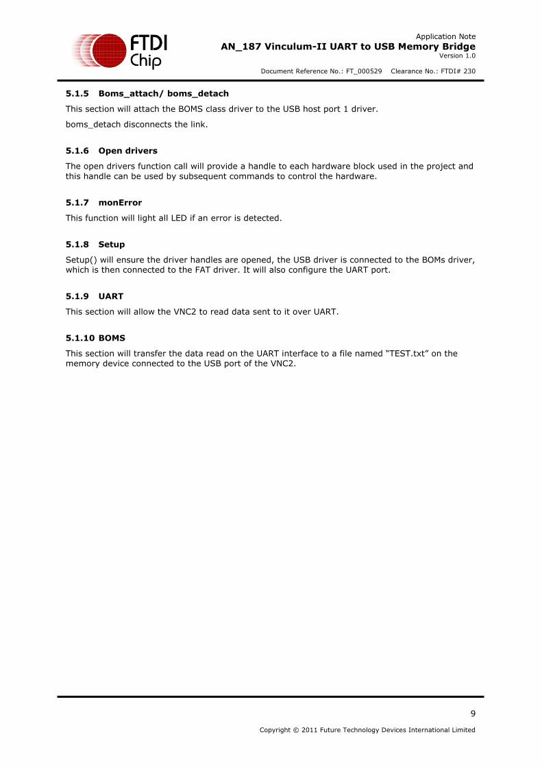
5.1.5 Boms_attach/ boms_detach ........................................................................................... 9
5.1.6 Open drivers .................................................................................................................... 9
5.1.7 monError ......................................................................................................................... 9
5.1.8 Setup ............................................................................................................................... 9
5.1.9 UART ................................................................................................................................ 9
5.1.10 BOMS .............................................................................................................................. 9
6 Contact Information ...................................................................................................................... 10
Appendix A – References ...................................................................................................................... 11
Acronyms and Abbreviations ............................................................................................................ 11
Appendix B – List of Tables & Figures ................................................................................................... 12
List of Tables ..................................................................................................................................... 12
List of Figures .................................................................................................................................... 12
Appendix C – Revision History .............................................................................................................. 13

Application Note
AN_187 Vinculum-II UART to USB Memory Bridge Version 1.0
Document Reference No.: FT_000529 Clearance No.: FTDI# 230
2
Copyright © 2011 Future Technology Devices International Limited
1 Introduction
FTDI have introduced a new suite of simplified “bridging” ROM files to allow for fast interconnect between differing interfaces. These ROM images (and sample code) are targeted at those users who would like to implement VNC2 into a design without creating their own firmware.
As well as providing the source code for users wishing to modify setup parameters the default project will be supplied as a precompiled ROM file ready for installation into the VNC2.
This application note forms part of a series of application notes detailing the new simplified ROM
images for VNC2. This document will detail the implementation and use of a VNC2 ROM file for bridging a UART interface to hosting a Bulk Only Mass storage (BOMS) class device on a USB port (USB memory). This particular project may be used in 32, 48 or 64 pin packages.
For users not intending to edit the code in any way the precompiled code may be loaded over the UART interface with FT_PROG as an alternative to using the IDE. Links for the project file, UART2DSC.vproj and the precompiled ROM file, Firmware.rom file may be found at the end of the document in Appendix A.
1.1 VNC2 Devices
VNC2 is the second of FTDI’s Vinculum family of embedded dual USB host controller devices. The VNC2 device provides USB Host interfacing capability for a variety of different USB device classes
including support for BOMS (bulk only mass storage), Printer and HID (human interface devices). For mass storage devices such as USB Flash drives, VNC2 transparently handles the FAT file structure.
Communication with non USB devices, such as a low cost microcontroller, is accomplished via
either UART, SPI or parallel FIFO interfaces. VNC2 provides a new, cost effective solution for providing USB Host capability into products that previously did not have the hardware resources available.
VNC2 allows customers to develop their own firmware using the Vinculum II software development tool suite. These development tools provide compiler, assembler, linker and debugger tools complete within an integrated development environment (IDE).
The Vinculum-II VNC2 family of devices are available in Pb-free (RoHS compliant) 32-lead LQFP, 32-lead QFN, 48-lead LQFP, 48-lead QFN, 64-Lead LQFP and 64-lead QFN packages For more information on the ICs refer to the VNC2 Product Page.

Application Note
AN_187 Vinculum-II UART to USB Memory Bridge Version 1.0
Document Reference No.: FT_000529 Clearance No.: FTDI# 230
3
Copyright © 2011 Future Technology Devices International Limited
2 Using the Sample Code
VNC2UART
DEVICE
UART DATA BOMS Class
PERIPHERAL
(USB Memory)
USB
12MHz
GND
DEBUGGER I/F
3V3
RE
SE
T
VC
CIO
3V
3V
RE
GIN
TE
ST
PR
OG
#
1V8
VR
EG
OU
T
1V
8 P
LL
IN
XT
IN
XT
OU
T
Figure 2.1 Connecting the Demo
When the VNC2 is programmed, the user simply passes data from the UART interface to the VNC2. This data will be appended to a file named “TEST.TXT”.
The default configuration of the UART port on the VNC2 is 9600-8-N-1, RTS_CTS flow control.
The project uses the VNC2 USB port 1.
There are no additional commands required; it is a simple data bridge.
2.1 LEDs
GPIO Lines A1, A2, A4 and A5 provide active low indicators that may be used to drive LEDs. Due to
the nature of the VNC2 MUX, not all indicators are available on all packages.
The LED on A1 is not programmed to provide a specific function.
The LED on A2 is not programmed to provide a specific function.
The LED on A4 will flash until enumeration is complete and then remain on.
The LED on A5 is not programmed to provide a specific function.
Note: connecting the LED anode to the VNC2 would allow the indication to be inverted.

Application Note
AN_187 Vinculum-II UART to USB Memory Bridge Version 1.0
Document Reference No.: FT_000529 Clearance No.: FTDI# 230
4
Copyright © 2011 Future Technology Devices International Limited
3 Default Pin-Out
The VNC2 can assign the same signal to a variety of pins. The default pins used for this ROM image are shown in Table 3.1.
Signal 32-pin pkg 48-pin pkg 64-pin pkg Description
GND 1, 16, 19, 27 1, 24, 27, 39 1, 30, 35, 53 Device ground supply pins
3V3 VREGIN 2 2 2 +3.3VDC supply to the regulator
1V8 VCC PLL IN 3 3 3
+1.8VDC supply to internal clock multiplier
Requires 100nF decoupling capacitor close to pin
GND PLL 6 6 6 Device analog ground supply for internal clock multiplier
VREG OUT 7 7* 7
+1.8VDC output from regulator to device core
*Not used on 48-pin LQFP package
VCCIO 13, 22, 28 17, 30, 40 21, 38, 54
+3.3VDC supply to I/O interface pins (IOBUS)
VCCIO must be connected for proper operation
XTIN 4 4 4
Input to 12MHz Oscillator
Connect 12MHz crystal across pins 4 and 5 with proper loading capacitance
XTOUT 5 5 5
Output from 12MHz Oscillator
Connect 12MHz crystal across pins 4 and 5 with proper loading capacitance
TEST 8 8 8 Test – Must be connected to GND for normal operation
RESET# 10 9 9 Can be used by an external device to reset VNC2
PROG# 9 10 10 Asserting PROG# enables program mode
DEBUGGER I/F 11 11 11 I/O for programming and in-circuit debugging
USB DP1 17 25 33 USB Port 1 Data Plus
USB DM1 18 26 34 USB Port 1 Data Minus

Application Note
AN_187 Vinculum-II UART to USB Memory Bridge Version 1.0
Document Reference No.: FT_000529 Clearance No.: FTDI# 230
5
Copyright © 2011 Future Technology Devices International Limited
Signal 32-pin pkg 48-pin pkg 64-pin pkg Description
UART RXD 24 32 40 UART data input to VNC2
UART TXD 23 31 39 UART data output from VNC2
UART RTS# 25 33 41
UART RTS# output from VNC2
Logic 0 implies the VNC2 can accept more data
UART CTS# 26 34 42
UART CTS# input to VNC2
Logic 0 allows the VNC2 to send more data on UART TXD
GPIO_A0 - - 61 GPIO signal used for LED
GPIO_A1 12 - 62 GPIO signal used for LED
GPIO_A2 14 46 63 GPIO signal used for LED
GPIO_A3 15 45 56 GPIO signal used for LED
GPIO_A4 - 48 48 GPIO signal used for LED
GPIO_A5 - 42 - GPIO signal used for LED
GPIO_A6 - 43 - GPIO signal used for LED
GPIO_A7 - - 64 GPIO signal used for LED
Table 3.1 VNC2 Default Pin-Out
Designers wanting to customise the design should refer to the UART2DSC_iomux.c file for changing pin-out options.

Application Note
AN_187 Vinculum-II UART to USB Memory Bridge Version 1.0
Document Reference No.: FT_000529 Clearance No.: FTDI# 230
6
Copyright © 2011 Future Technology Devices International Limited
4 Building and Loading the Firmware into the VNC2
Everything can be controlled by the IDE. To access the application simply use the Project -> Open tab to browse to the UART2DSC.vproj file for your project.
Figure 4.1 Vinculum-II Project Open Button
4.1 Build
This step is only necessary if you are not using the precompiled version of the ROM. Otherwise proceed to loading the ROM file.
To build the application you simply press the Build button on the IDE ribbon bar under the build
tab.
Figure 4.2 Vinculum-II IDE Build Button
4.2 Load
Loading the code is equally simple. Just click on the “Flash” button on the ribbon bar under the debug tab. The Flash button will automatically pick up the Rom file in your project but for
reference the filename is UART2DSC .ROM.
Figure 4.3 Vinculum-II IDE Flash Button
Note the Debugger Interface is listed as V2EVAL Board C. It is important that this box shows a device is connected before attempting to flash a device.

Application Note
AN_187 Vinculum-II UART to USB Memory Bridge Version 1.0
Document Reference No.: FT_000529 Clearance No.: FTDI# 230
7
Copyright © 2011 Future Technology Devices International Limited
4.3 Loading with FT_Prog
If the precompiled ROM file meets all the requirements of the end design then the IDE and source code are not required. The precompiled HIDUart.ROM file may be loaded into the VNC2 with FT_PROG over the UART interface.
FT_Prog is used to program the VNC2 with a ROM file. FT_Prog is available from the FTDI website utilities page (version 1.12 or later supports VNC2).
Select the flash ROM tab at the top of the window.
Select VNC2 from the pull down tab.
Select D2xx or VCP interface (either will work).
Select the location where the ROM file resides.
Press the program button.
Perform a hard reset (power cycle) prior to running the firmware.
Figure 4.4 is an example of programming the VNC2 Evaluation board revision 2 with the V2DAP firmware.
Figure 4.4 FT_Prog Programming Utility
For more information on loading ROM files onto a VNC2 device refer to:
AN_159_Vinculum_II_Firmware_Flash_Programming.pdf

Application Note
AN_187 Vinculum-II UART to USB Memory Bridge Version 1.0
Document Reference No.: FT_000529 Clearance No.: FTDI# 230
8
Copyright © 2011 Future Technology Devices International Limited
5 Source Code for the VNC2 Application
This section is aimed at those wanting to learn about coding VNC2 devices or modify the existing project.
All VNC2 application firmware follows a similar format and most of the code can be “written” using the IDE application wizard.
The basic steps are:
Initialise device drivers
Define pin-outs
Open ports to be used
Configure ports to be used
Read/write data
Close ports
The VNC2 source code for this project can be viewed in appendix A and is available to download
with the toolchain.
5.1 UART2DSC.C
void main(); void iomux_setup(void); unsigned char usbhost_connect_state(VOS_HANDLE hUSB) VOS_HANDLE fat_attach(VOS_HANDLE hMSI, unsigned char devFAT) void fat_detach(); VOS_HANDLE boms_attach(VOS_HANDLE hUSB, unsigned char devBOMS) void boms_detach(); void open_drivers(void); void monError(void); void setup(); void UART(void) void BOMS(void)
5.1.1 main()
Main is where the application starts. It defines the VNC2 core clock speed, loads the drivers to be used and creates the threads to be used in the application. At the very end of main is the call
vos_start_scheduler();
After this call there can be no further configuration of the device.
5.1.2 Iomux_setup()
Iomux_setup actually refers to the other file in the project, SPI2DSC_iomux.c and is used to define the VNC2 pin-out. Most functions can be programmed to appear on different pins. The notable exceptions are power, GND and the USB ports.
5.1.3 USB_Host_Connect_state
USB_Host_Connect_State is a function to check if anything is connected to the USB host.
5.1.4 Fat_attach/ Fat_detach
This section will attach the FAT driver to the BOMS class driver. This is the last layer of the driver construction to connect the USB port to a FAT table in a memory device. Fat_detach disconnects the link.
Application Note
AN_187 Vinculum-II UART to USB Memory Bridge Version 1.0
Document Reference No.: FT_000529 Clearance No.: FTDI# 230
9
Copyright © 2011 Future Technology Devices International Limited
5.1.5 Boms_attach/ boms_detach
This section will attach the BOMS class driver to the USB host port 1 driver.
boms_detach disconnects the link.
5.1.6 Open drivers
The open drivers function call will provide a handle to each hardware block used in the project and
this handle can be used by subsequent commands to control the hardware.
5.1.7 monError
This function will light all LED if an error is detected.
5.1.8 Setup
Setup() will ensure the driver handles are opened, the USB driver is connected to the BOMs driver, which is then connected to the FAT driver. It will also configure the UART port.
5.1.9 UART
This section will allow the VNC2 to read data sent to it over UART.
5.1.10 BOMS
This section will transfer the data read on the UART interface to a file named “TEST.txt” on the memory device connected to the USB port of the VNC2.

Application Note
AN_187 Vinculum-II UART to USB Memory Bridge Version 1.0
Document Reference No.: FT_000529 Clearance No.: FTDI# 230
10
Copyright © 2011 Future Technology Devices International Limited
6 Contact Information
Head Office – Glasgow, UK Future Technology Devices International Limited Unit 1, 2 Seaward Place, Centurion Business Park Glasgow G41 1HH United Kingdom Tel: +44 (0) 141 429 2777 Fax: +44 (0) 141 429 2758 E-mail (Sales) [email protected] E-mail (Support) [email protected] E-mail (General Enquiries) [email protected]
Branch Office – Taipei, Taiwan Future Technology Devices International Limited (Taiwan) 2F, No. 516, Sec. 1, NeiHu Road
Taipei 114 Taiwan , R.O.C. Tel: +886 (0) 2 8791 3570 Fax: +886 (0) 2 8791 3576 E-mail (Sales) [email protected] E-mail (Support) [email protected] E-mail (General Enquiries) [email protected]
Branch Office – Hillsboro, Oregon, USA Future Technology Devices International Limited (USA) 7235 NW Evergreen Parkway, Suite 600 Hillsboro, OR 97123-5803 USA Tel: +1 (503) 547 0988 Fax: +1 (503) 547 0987 E-Mail (Sales) [email protected] E-Mail (Support) [email protected] E-Mail (General Enquiries) [email protected]
Branch Office – Shanghai, China Future Technology Devices International Limited (China) Room 408, 317 Xianxia Road,
Shanghai, 200051 China Tel: +86 21 62351596 Fax: +86 21 62351595 E-mail (Sales) [email protected] E-mail (Support) [email protected] E-mail (General Enquiries) [email protected]
Web Site http://ftdichip.com
System and equipment manufacturers and designers are responsible to ensure that their systems, and any Future Technology
Devices International Ltd (FTDI) devices incorporated in their systems, meet all applicable safety, regulatory and system-level
performance requirements. All application-related information in this document (including application descriptions, suggested
FTDI devices and other materials) is provided for reference only. While FTDI has taken care to assure it is accurate, this
information is subject to customer confirmation, and FTDI disclaims all liability for system designs and for any applications assistance provided by FTDI. Use of FTDI devices in life support and/or safety applications is entirely at the user’s risk, and the
user agrees to defend, indemnify and hold harmless FTDI from any and all damages, claims, suits or expense resulting from
such use. This document is subject to change without notice. No freedom to use patents or other intellectual property rights is
implied by the publication of this document. Neither the whole nor any part of the information contained in, or the product
described in this document, may be adapted or reproduced in any material or electronic form without the prior written consent
of the copyright holder. Future Technology Devices International Ltd, Unit 1, 2 Seaward Place, Centurion Business Park,
Glasgow G41 1HH, United Kingdom. Scotland Registered Company Number: SC136640

Application Note
AN_187 Vinculum-II UART to USB Memory Bridge Version 1.0
Document Reference No.: FT_000529 Clearance No.: FTDI# 230
11
Copyright © 2011 Future Technology Devices International Limited
Appendix A – References
Application and Technical Notes available at http://www.ftdichip.com/Support/Documents/AppNotes.htm
VNC2 Datasheet
V2-EVAL datasheet
Vinculum II Toolchain
AN_139 IO_Mux explained
AN_151 Vinculum II User Guide
AN_159_Vinculum_II_Firmware_Flash_Programming.pdf
Project source code download
www.ftdichip.com/Firmware/Precompiled/UART2DSC.zip
Project precompiled ROM file download
www.ftdichip.com/Firmware/Precompiled/Firmware.ROM
Acronyms and Abbreviations
Terms Description
UART Universal Asynchronous Receiver Transmitter
USB Universal Serial Bus
USB-IF USB Implementers Forum
NOTE – put terms in alphabetical order.

Application Note
AN_187 Vinculum-II UART to USB Memory Bridge Version 1.0
Document Reference No.: FT_000529 Clearance No.: FTDI# 230
12
Copyright © 2011 Future Technology Devices International Limited
Appendix B – List of Tables & Figures
List of Tables
Table 3.1 VNC2 Default Pin-Out ............................................................................................ 5
List of Figures
Figure 2.1 Connecting the Demo ........................................................................................... 3
Figure 4.1 Vinculum-II Project Open Button ........................................................................... 6
Figure 4.2 Vinculum-II IDE Build Button ................................................................................ 6
Figure 4.3 Vinculum-II IDE Flash Button ................................................................................ 6
Figure 4.4 FT_Prog Programming Utility ................................................................................. 7

Application Note
AN_187 Vinculum-II UART to USB Memory Bridge Version 1.0
Document Reference No.: FT_000529 Clearance No.: FTDI# 230
13
Copyright © 2011 Future Technology Devices International Limited
Appendix C – Revision History
Document Title: AN_187 Vinculum-II UART to USB Memory Bridge
Document Reference No.: FT_000529
Clearance No.: FTDI# 230
Product Page: http://www.ftdichip.com/Products/ICs/VNC2.htm
Document Feedback: Send Feedback
Revision Changes Date
1.0 Initial Release 2011-11-02