
Vertical-Cavity Surface-Emitting Laser TechnologyPrinceton Optronics, Inc. * 1 Electronics Drive *...
17
Princeton Optronics, Inc. * 1 Electronics Drive * Mercerville, New Jersey 08619 Voice: (609) 584-9696 * Fax: (609) 584-2448 * E-mail: [email protected] * www.princetonoptronics.com Vertical-Cavity Surface-Emitting Laser Technology Introduction Vertical-Cavity Surface-Emitting Lasers (VCSELs) are a relatively recent type of semiconductor lasers. VCSELs were first invented in the mid-1980’s. Very soon, VCSELs gained a reputation as a superior technology for short reach applications such as fiber channel, Ethernet and intra-systems links. Then, within the first two years of commercial availability (1996), VCSELs became the technology of choice for short range datacom and local area networks, effectively displacing edge-emitter lasers. This success was mainly due to the VCSEL’s lower manufacturing costs and higher reliability compared to edge-emitters. Princeton Optronics has developed the key technologies resulting in the world's highest power single VCSEL devices and 2-D arrays. We have successfully demonstrated single devices with >5W CW output power and large 2D arrays with >230W CW output power. We have made single mode devices of 1W output power and single mode arrays with power of >100W which are coupled to 100u, 0.22NA fiber. The highest wall plug efficiency of these devices and arrays is 56%. We have made arrays which deliver 1kW/cm2 in CW operation and 4.2kW/cm2 in QCW operation. Princeton Optronics was a participant in the DARPA-SHEDS program, whose main objective was to improve laser diode conversion efficiency. The VCSEL structure Semiconductor lasers consist of layers of semiconductor material grown on top of each other on a substrate (the “epi”). For VCSELs and edge-emitters, this growth is typically done in a molecular-beam-epitaxy (MBE) or metal- organic-chemical-vapor-deposition (MOCVD) growth reactor. The grown wafer is then processed accordingly to produce individual devices. Figure 1 summarizes the differences between VCSEL and edge-emitter processing. Figure 1. Comparison of the growth/processing flow of VCSEL and edge-emitter semiconductor lasers.
Transcript of Vertical-Cavity Surface-Emitting Laser TechnologyPrinceton Optronics, Inc. * 1 Electronics Drive *...

Princeton Optronics, Inc. * 1 Electronics Drive * Mercerville, New Jersey 08619
Voice: (609) 584-9696 * Fax: (609) 584-2448 * E-mail: [email protected] * www.princetonoptronics.com
Vertical-Cavity Surface-Emitting Laser Technology
Introduction
Vertical-Cavity Surface-Emitting Lasers (VCSELs) are a relatively recent type of semiconductor lasers. VCSELs were first invented in the mid-1980’s. Very soon, VCSELs gained a reputation as a superior technology for short reach applications such as fiber channel, Ethernet and intra-systems links. Then, within the first two years of commercial availability (1996), VCSELs became the technology of choice for short range datacom and local area networks, effectively displacing edge-emitter lasers. This success was mainly due to the VCSEL’s lower manufacturing costs and higher reliability compared to edge-emitters.
Princeton Optronics has developed the key technologies resulting in the world's highest power single VCSEL devices and 2-D arrays. We have successfully demonstrated single devices with >5W CW output power and large 2D arrays with >230W CW output power. We have made single mode devices of 1W output power and single mode arrays with power of >100W which are coupled to 100u, 0.22NA fiber. The highest wall plug efficiency of these devices and arrays is 56%. We have made arrays which deliver 1kW/cm2 in CW operation and 4.2kW/cm2 in QCW operation. Princeton Optronics was a participant in the DARPA-SHEDS program, whose main objective was to improve laser diode conversion efficiency.
The VCSEL structure
Semiconductor lasers consist of layers of semiconductor material grown on top of each other on a substrate (the “epi”). For VCSELs and edge-emitters, this growth is typically done in a molecular-beam-epitaxy (MBE) or metal-organic-chemical-vapor-deposition (MOCVD) growth reactor. The grown wafer is then processed accordingly to produce individual devices. Figure 1 summarizes the differences between VCSEL and edge-emitter processing.
Figure 1. Comparison of the growth/processing flow of VCSEL and edge-emitter semiconductor lasers.

Princeton Optronics, Inc. * 1 Electronics Drive * Mercerville, New Jersey 08619
Voice: (609) 584-9696 * Fax: (609) 584-2448 * E-mail: [email protected] * www.princetonoptronics.com
In a VCSEL, the active layer is sandwiched between two highly reflective mirrors (dubbed distributed Bragg reflectors, or DBRs) made up of several quarter-wavelength-thick layers of semiconductors of alternating high and low refractive index. The reflectivity of these mirrors is typically in the range 99.5~99.9%. As a result, the light oscillates perpendicular to the layers and escapes through the top (or bottom) of the device. Current and/or optical confinement is typically achieved through either selective-oxidation of an Aluminum-rich layer, ion-implantation, or even both for certain applications. The VCSELs can be designed for “top-emission” (at the epi/air interface) or “bottom-emission” (through the transparent substrate) in cases where “junction-down” soldering is required for more efficient heat-sinking for example. Figure 2 illustrates different common types of VCSEL structures. In contrast, edge-emitters are made up of cleaved bars diced from the wafers. Because of the high index of refraction contrast between air and the semiconductor material, the two cleaved facets act as mirrors. Hence, in the case of an edge-emitter, the light oscillates parallel to the layers and escapes side-ways. This simple structural difference between the VCSEL and the edge-emitter has important implications.
Since VCSELs are grown, processed and tested while still in the wafer form, there is significant economy of scale resulting from the ability to conduct parallel device processing, whereby equipment utilization and yields are maximized and set up times and labor content are minimized. In the case of a VCSEL (see Figure 1), the mirrors and active region are sequentially stacked along the Y axis during epitaxial growth. The VCSEL wafer then goes through etching and metalization steps to form the electrical contacts. At this point the wafer goes to test where individual laser devices are characterized on a pass-fail basis. Finally, the wafer is diced and the lasers are binned for either higher-level assembly (typically >95%) or scrap (typically <5%). The following Figure shows a single high-power VCSEL device (>2W output power) packaged on a high-thermal conductivity submount.
Substrate
Heat-spreader
Light output
N-contact
DBRsActive
region
P-contact
Substrate
Substrate
Proton
implantation
Oxide
aperture
Oxide
aperture
(a)
(b)
(c)
Substrate
Heat-spreader
Light output
N-contact
DBRsActive
region
P-contact
Substrate
Substrate
Proton
implantation
Oxide
aperture
Oxide
aperture
(a)
(b)
(c)
Figure 2. Three common types of VCSEL structures: (a) a top-emitting structure with proton implantation to confine the current, (b) a selectively-oxidized top-emitting structure to confine the optical modes and/or the current, and (c) a mounted bottom-emitting selectively-oxidized structure.
Figure 3.
Packaged high-power VCSEL
device (>2W). The submount is
2mm x 2mm.

Princeton Optronics, Inc. * 1 Electronics Drive * Mercerville, New Jersey 08619
Voice: (609) 584-9696 * Fax: (609) 584-2448 * E-mail: [email protected] * www.princetonoptronics.com
In a simple Fabry-Pérot edge-emitter the growth process also occurs along the Y axis, but only to create the active region as mirror coatings are later applied along the Z axis. After epitaxial growth, the wafer goes through the metallization step and is subsequently cleaved along the X axis, forming a series of wafer strips. The wafer strips are then stacked and mounted into a coating fixture. The Z axis edges of the wafer strips are then coated to form the device mirrors. This coating is a critical processing step for edge-emitters, as any coating imperfection will result in early and catastrophic failure of the devices due to catastrophic-optical-damage (COD). After this coating step, the wafer strips are diced to form discrete laser chips, which are then mounted onto carriers. Finally, the laser devices go into test. It is also important to understand that VCSELs consume less material: in the case of a 3” wafer, a laser manufacturer can build about 15,000 VCSEL devices or approximately 4,000 edge-emitters of similar power levels. In addition to these advantages, VCSEL also demonstrate excellent dynamic performances such as low threshold currents (a few micro-amps), low noise operation and high-speed digital modulation (10 Gb/s). Furthermore, although VCSELs have been confined to low-power applications – a few milli-Watts at most – they have the inherent potential of producing very high powers by processing large 2-D arrays. In contrast, edge-emitters cannot be processed in 2-D arrays.
VCSEL advantages
The many advantages offered by the VCSEL technology can be summarized in the following points:
1. Wavelength stability: The lasing wavelength in a VCSEL is very stable, since it is fixed by the short (1~1.5-wavelength thick) Fabry-Perot cavity. Contrary to edge-emitters, VCSELs can only operate in a single longitudinal mode.
2. Wavelength uniformity & spectral width: Growth technology has improved such that VCSEL 3” wafers are produced with less then a 2nm standard deviation for the cavity wavelength. This allows for the fabrication of VCSEL 2-D arrays with little wavelength variation between the elements of the array (<1nm full-width half-maximum spectral width). By contrast, edge-emitter bar-stacks suffer from significant wavelength variations from bar to bar since there is no intrinsic mechanism to stabilize the wavelength, resulting in a wide spectral width (3~5nm FWHM).
3. Temperature sensitivity of wavelength: The emission wavelength in VCSELs is ~5 times less sensitive to temperature variations than in edge-emitters. The reason is that in VCSELs, the lasing wavelength is defined by the optical thickness of the single-longitudinal-mode-cavity and that the temperature dependence of this optical thickness is minimal (the refractive index and physical thickness of the cavity have a weak dependence on temperature). On the other hand, the lasing wavelength in edge-emitters is defined by the peak-gain wavelength, which has a much stronger dependence on temperature. As a consequence, the spectral line-width for high-power arrays (where heating and temperature gradients can be significant) is much narrower in VCSEL arrays than in edge-emitter-arrays (bar-stacks). Also, over a 20oC change in temperature, the emission wavelength in a VCSEL will vary by less than 1.4nm (compared to ~7nm for edge-emitters).
4. High Temperature Operation (Chillerless operation for pumps: VCSEL devices can be operated without refrigeration- because they can be operated at temperatures to 80 deg C, The cooling system becomes very small, rugged and portable with this approach.
5. Higher power per unit area: Edge emitters deliver a maximum of about 500W/cm2 because of gap between bar to bar which has to be maintained for coolant flow, while VCSELs are delivering ~1200W/ cm2 now and can deliver 2-4kW/ cm2 in near future.
6. Beam Quality: VCSELs emit a circular beam. Through proper cavity design VCSELs can also emit in a single transverse mode (circular Gaussian). This simple beam structure greatly reduces the complexity and cost of coupling/beam-shaping optics (compared to edge-emitters) and increases the coupling efficiency to the fiber or pumped medium. This has been a key selling point for the VCSEL technology in low-power markets.
7. Reliability: Because VCSELs are not subject to catastrophic optical damage (COD), their reliability is much higher than for edge-emitters. Typical FIT values (failures in one billion device-hours) for VCSELs are <10.
8. Manufacturability and yield: Manufacturability of VCSELs has been a key selling point for this technology. Because of complex manufacturing processes and reliability issue related to COD (catastrophic optical damage), edge-emitters have a low yield (edge-emitter 980nm pump chip manufacturers typically only get ~500 chips out of a 2” wafer). On the other hand, yields for VCSELs exceed 90% (corresponds to ~5000 high-power chips from a 2” wafer). In fact, because of its planar attributes, VCSEL manufacturing is identical to standard IC Silicon processing.
9. Scalability: For high-power applications, a key advantage of VCSELs is that they can be directly processed into monolithic 2-D arrays, whereas this is not possible for edge-emitters (only 1-D monolithic arrays are possible). In addition, a complex and thermally inefficient mounting scheme is required to mount edge-emitter bars in stacks.

Princeton Optronics, Inc. * 1 Electronics Drive * Mercerville, New Jersey 08619
Voice: (609) 584-9696 * Fax: (609) 584-2448 * E-mail: [email protected] * www.princetonoptronics.com
10. Packaging and heat-sinking: Mounting of large high-power VCSEL 2-D arrays in a “junction-down” configuration is straightforward (similar to micro-processor packaging), making the heat-removal process very efficient, as the heat has to traverse only a few microns of AlGaAs material. Record thermal impedances of <0.16K/W have been demonstrated for 5mm x 5mm 2-D VCSEL arrays.
11. Cost: With the simple processing and heat-sinking technology it becomes much easier to package 2-D VCSEL arrays than an equivalent edge-emitter bar-stack. The established existing silicon industry heat-sinking technology can be used for heat removal for very high power arrays. This will significantly reduce the cost of the high-power module. Currently, cost of the laser bars is the dominant cost for the DPSS lasers.
High Wavelength Stability and Low Temperature Dependence
Since the VCSEL resonant cavity is defined by a wavelength-thick cavity sandwiched between two distributed Bragg reflectors (DBRs), devices emit in a single longitudinal mode and the emission wavelength is inherently stable (<0.07nm/K), without the need for additional wavelength stabilization schemes or external optics, as is the case for edge-emitters. Furthermore, thanks to advances in growth and packaging technologies, the emission wavelength is very uniform across a 5mm x 5mm VCSEL array, resulting in spectral widths of 0.7~0.8nm (full-width at half-maximum). This wavelength stability and narrow spectral width can be very significant advantages in pumping applications for example where the medium has a narrow absorption band.
Circular output beam Unlike edge-emitters, VCSELs emit in a circularly symmetric beam with low divergence without the need for additional optics. This has been a tremendous advantage for low-power VCSELs in the telecom and datacom markets because of their ability to directly couple to fibers (“butt-coupling”) with high coupling efficiency. Princeton Optronics’ high-power VCSEL arrays emit in a quasi-top-hat beam profile, making these devices ideal for direct pumping (“butt-pumping”) of solid-state lasers.
Feedback insensitivity
In VCSELs, the as-grown output coupler reflectivity is very high (typically >99.5%) compared to edge-emitters (typically <5%). This makes VCSELs extremely insensitive to optical feedback effects, thus eliminating the need for expensive isolators or filters in some applications. Low thermal impedance & ease of packaging Princeton Optronics has developed advanced packaging technologies, which enables efficient and reliable die-attach of large 2-D VCSEL arrays on high-thermal-conductivity submounts. The resulting submodule layout allows for straightforward packaging on a heat-exchanger.
Figure 4. Emission spectrum of a 5mm x 5mm VCSEL array at 100W output power (120A).
Figure 5. Far-field beam profile of a 5mm x 5mm VCSEL array at 100W output power (120A).
0 10 0
5 10 -4
1 10 -3
2 10 -3
2 10 -3
3 10 -3
964 966 968 970 972 974
Signal (mW)
Wavelength (nm)
FWHM~0.8nm

Princeton Optronics, Inc. * 1 Electronics Drive * Mercerville, New Jersey 08619
Voice: (609) 584-9696 * Fax: (609) 584-2448 * E-mail: [email protected] * www.princetonoptronics.com
For high-power devices packaged on micro-coolers, Princeton Optronics has demonstrated modules with thermal impedances as low as 0.15K/W (between the chiller and the chip active layer). Princeton Optronics can provide its customers with several heat-exchanger and heat-sinking application notes.
High Power CW and QCW VCSEL Arrays:
Princeton Optronics designs and manufactures advanced high-power CW and QCW diode lasers for the industrial, medical, and defense markets. Princeton Optronics’ innovative approach is based on the Vertical-Cavity Surface-Emitting Laser technology (VCSEL for short), enabling us to manufacture and deliver laser diodes with exceptionally high reliability, and superior spectral and beam properties.
Arrays with Hundreds of Watts (>1kW/cm2 Power Density) Output Power:
Vertical-Cavity Surface-Emitting Lasers were initially introduced in the mid-90’s as a low-cost alternative to edge-emitters, for use as a low-power source (sub-mW to a few mW) in datacoms and telecoms. Within two years of their introduction, VCSELs overwhelmed and replaced the edge-emitter technology in these markets due to their better beam quality, reduced manufacturing costs and much higher reliability. Now, a new class of VCSELs has been developed for high power applications. Princeton Optronics is the first company to introduce such high power VCSEL products to the market. Unlike edge-emitters, the light emits perpendicular to wafer surface for VCSELs. It is therefore straightforward to process 2-D arrays of small VCSEL devices driven in parallel to obtain higher output powers. The advantage of 2D arrays is that it has simple silicon IC chip-like configuration and many of the silicon IC packaging and cooling technology can be applied to VCSEL arrays. Princeton Optronics has taken the VCSEL technology to very high power levels by developing very large (5mm x 5mm) 2-D VCSEL arrays packaged on high-thermal-conductivity submounts. These arrays are composed of thousands of low-power single devices driven in parallel. Using this approach, record CW output powers in excess of 230W from a 0.22cm2 emission area (>1kW/cm2) have been demonstrated, without sacrificing wall-plug efficiency.
Very high-power density QCW operation
In addition to CW VCSEL arrays, Princeton Optronics has developed very high power density VCSEL arrays for quasi-CW (QCW) operation. QCW powers in excess of 925W have been demonstrated from very small arrays (5x5mm chip size), resulting in record power densities >4.2kW/cm2. These small arrays can easily be connected in series to form larger arrays with high output powers.
Figure 6. Picture of high-power 5mm x 5mm 2-D VCSEL array mounted on a micro-cooler and
measure CW output power and voltage at a constant heat-sink temperature. Roll-over power is
>230W.
0
50
100
150
200
250
0 50 100 150 200 250 300
Outp
ut
Po
wer
(W)
Current (A)

Princeton Optronics, Inc. * 1 Electronics Drive * Mercerville, New Jersey 08619
Voice: (609) 584-9696 * Fax: (609) 584-2448 * E-mail: [email protected] * www.princetonoptronics.com
These arrays are ideal for applications requiring very compact high-power laser sources.
High Temperature Operation
Because VCSELs can operate reliably at temperatures up to 80 oC, they do not necessarily require refrigeration. Additionally, since the wavelength change with temperature is small, the cooling system design can be considerably simplified. The cooling system thus becomes very small, rugged and portable with this approach. We have been operating the VCSELs and VCSEL arrays with water pump and a radiator cooling like that of a car engine. Fig 2 shows such a set up in which a radiator and water pump is used to cool a 120W array of VCSELs. The result of the cooling arrangement is compared with a chiller cooling and shown in Fig 3.
Fig 8. Shows the set up without chiller using a radiator and a water pump in an arrangement like in a car engine.
Figure 7. Power vs. current for a small VCSEL 2D array under different QCW regimes. These arrays exhibit power densities >4.2kW/cm2.
0
200
400
600
800
1000
0
20
40
60
80
100
0 500 1000 1500 2000
Output Power OUT (W)
PCE (%)
Outp
ut P
ow
er
OU
T (
W)
PC
E (
%)
Electrical Power IN (W)
50.4%
420W
976nm VCSEL array chip
0.22 cm2 emission area
Princeton Optronics, Inc. * 1 Electronics Drive * Mercerville, New Jersey 08619
Voice: (609) 584-9696 * Fax: (609) 584-2448 * E-mail: [email protected] * www.princetonoptronics.com
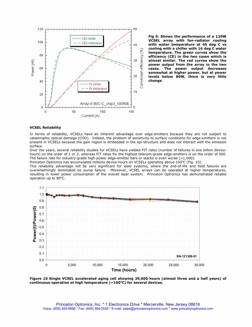
Fig 9. Shows the performance of a 120W VCSEL array with fan-radiator cooling with water temperature at 45 deg C vs cooling with a chiller with 16 deg C water temperature. The green curves show the efficiency (CE) in the two cases which is almost similar. The red curves show the power output from the array in the two cases. The power output decreases somewhat at higher power, but at power levels below 80W, there is very little change.
VCSEL Reliability
In terms of reliability, VCSELs have an inherent advantage over edge-emitters because they are not subject to catastrophic optical damage (COD). Indeed, the problem of sensitivity to surface conditions for edge-emitters is not present in VCSELs because the gain region is embedded in the epi-structure and does not interact with the emission surface. Over the years, several reliability studies for VCSELs have yielded FIT rates (number of failures in one billion device-hours) on the order of 1 or 2, whereas FIT rates for the highest telecom-grade edge-emitters is on the order of 500. The failure rate for industry-grade high-power edge-emitter bars or stacks is even worse (>1,000). Princeton Optronics has accumulated millions device-hours on VCSELs operating above 100oC (Fig. 10). This reliability advantage will be very significant for laser systems, where the end-of-life and field failures are overwhelmingly dominated by pump failure. Moreover, VCSEL arrays can be operated at higher temperatures, resulting in lower power consumption of the overall laser system. Princeton Optronics has demonstrated reliable operation up to 80oC.
RA-121306-01
0.0
0.1
0.2
0.3
0.4
0.5
0.6
0.7
0.8
0.9
1.0
1.1
0 5,000 10,000 15,000 20,000 25,000 30,000
Time (hours)
Po
wer(
t)/P
ow
er(
0)
Figure 10 Single VCSEL accelerated aging cell showing 29,600 hours (almost three and a half years) of continuous operation at high temperature (~100oC) for several devices.

Princeton Optronics, Inc. * 1 Electronics Drive * Mercerville, New Jersey 08619
Voice: (609) 584-9696 * Fax: (609) 584-2448 * E-mail: [email protected] * www.princetonoptronics.com
Single Mode VCSEL Devices:
We make single mode devices with power level of 5mW for small aperture devices (4u) as well as higher power devices of power output of 150mW from a 100u aperture devices in TO can packages and upto 1W of a single device in a larger package. The devices have narrow linewidth of tens of kHz and SMSR of >30dB. The devices have high efficiency of >40%. Fig 11 shows the L-I characteristics as well as SMSR of a single mode low power device.
Fig 11a. (left) L-I characteristic of a 5u aperture VCSEL device. (right). Is the SMSR of the device.
Fig 11b. High temperature performance of a single mode device at temperatures upto 60 deg C. The power conversion efficiency (PCE) is 30% at 60 deg C and the power is >4mW at that temperature. At 95C: record 3mW single-mode power with 25.1% PCE..
-90
-85
-80
-75
-70
-65
-60
-55
-50
970.0 970.5 971.0 971.5 972.0 972.5 973.0 973.5 974.0
5mA (single mode)
Le
vel (d
Bm
)
Wavelength (nm)
33dB SMSR
LP01
0
1
2
3
4
5
6
7
8
0
10
20
30
40
50
60
70
80
0 2 4 6 8 10 12
5m-diam. aperture
Po
wer
(mW
)
Co
nvers
ion e
ffic
iency (
%)
Current (mA)
4mW
single-mode
Princeton Optronics, Inc. * 1 Electronics Drive * Mercerville, New Jersey 08619
Voice: (609) 584-9696 * Fax: (609) 584-2448 * E-mail: [email protected] * www.princetonoptronics.com
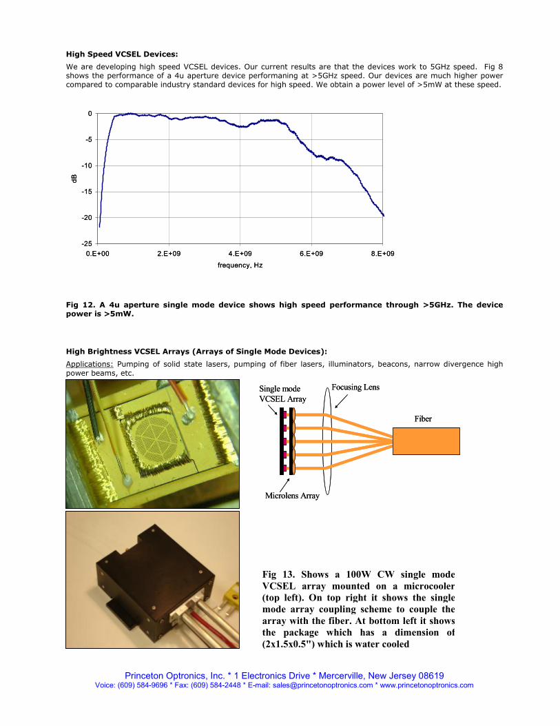
High Speed VCSEL Devices:
We are developing high speed VCSEL devices. Our current results are that the devices work to 5GHz speed. Fig 8 shows the performance of a 4u aperture device performaning at >5GHz speed. Our devices are much higher power compared to comparable industry standard devices for high speed. We obtain a power level of >5mW at these speed.
-25
-20
-15
-10
-5
0
0.E+00 2.E+09 4.E+09 6.E+09 8.E+09
frequency, Hz
dB
-25
-20
-15
-10
-5
0
0.E+00 2.E+09 4.E+09 6.E+09 8.E+09
frequency, Hz
dB
Fig 12. A 4u aperture single mode device shows high speed performance through >5GHz. The device power is >5mW.
High Brightness VCSEL Arrays (Arrays of Single Mode Devices):
Applications: Pumping of solid state lasers, pumping of fiber lasers, illuminators, beacons, narrow divergence high power beams, etc.
Single mode
VCSEL Array
Microlens Array
Focusing Lens
Fiber
Single mode
VCSEL Array
Microlens Array
Focusing Lens
Fiber
Fig 13. Shows a 100W CW single mode
VCSEL array mounted on a microcooler
(top left). On top right it shows the single
mode array coupling scheme to couple the
array with the fiber. At bottom left it shows
the package which has a dimension of
(2x1.5x0.5") which is water cooled

Princeton Optronics, Inc. * 1 Electronics Drive * Mercerville, New Jersey 08619
Voice: (609) 584-9696 * Fax: (609) 584-2448 * E-mail: [email protected] * www.princetonoptronics.com
VCSELs (vertical cavity surface emitting lasers) is a new technology for pumping of solid state lasers, including fiber lasers. Because of their circular beam and excellent optical characteristics, it is possible to make high brightness pumps using an array of closely spaced single mode VCSEL devices. The arrays are temperature stable and operate at high temperatures without chillers. They are lower cost as they do not need expensive operations like cleaving of the wafers. These fiber coupled arrays can be combined for higher output power using fiber combiners and coupled with double core fiber to develop small, high performance fiber lasers working at elevated temperatures without chillers.
For high brightness devices and arrays, Princeton Optronics makes self lasing VCSELs or extended or external cavity VCSELs and couples such arrays into fibers using microlenses as shown in Figure 13. Advantages of the VCSELs for fiber laser pumping applications are the following:
(i) Circular beam output and ease of coupling with fiber-individual VCSEL devices and arrays are known for easier coupling to fibers because of their circular beam and does not need complicated beam shaping optics. It is possible to couple them to fibers with very high efficiency.
(ii) Can be operated at high temperature without refrigeration- can be operated at temperatures to 80 deg C, and are cooled by a water pump and fan/radiator combination similar to the way the automobile engines are cooled. The cooling system becomes very small, rugged and portable with this approach.
(iii) Higher power from the array- VCSELs arrays are now delivering 230W from a 4.7 x 4.7mm aperture (>1kW/ cm2 )- and by fabricating a large 10x10mm array with the same power density we can obtain >1kW power which can be coupled to a fiber.
(iv) Higher reliability and life expectancy (50x) than edge emitters , resulting from removal of the junction from the emission facet and lower output power-density. This greatly reduces the maintenance needs and increases the life expectancy of solid state and fiber lasers which is dominated by pump life.
(v) Superior linewidth and stability, The typical linewidth from a 200W array is <0.8nm and temperature dependence is 0.06nm/deg C which are both much better compared to the edge emitters- highly beneficial to most solid state laser systems.
(vi) Much lower cost of gallium arsenide VCSEL chips and pump modules, resulting from gallium arsenide IC chip like manufacturing technology and similar simple packaging technique. The VCSELs already replaced the edge emitters in the low power applications for their lower cost, beam quality and high reliability. They can be 10x lower cost compared to the edge emitters as has been the case in the low power applications.
Princeton Optronics has demonstrated a coupling efficiency of 70% using a commercial off the shelf microlens array which was not the most optimum match for their 100W single mode array. The coupling scheme is shown in fig 1 along with a package. With a custom microlens array, our simulation shows that we should get a coupling efficiency of >90%. We developed a laser welded small package (2x1.5x0.5") which is able to handle a heat load of 500W (Fig 1)
Blue, Green and UV Laser:
Applications: Projection displays, undersea communications, read/write for optical storage etc.
Blue Laser from Frequency Doubled VCSEL Devices
Princeton Optronics has developed very high quality blue lasers from VCSEL devices. It uses its VCSEL technology and frequency double the VCSEL radiation by using a non-linear material. The blue laser output at 480nm is single mode and highly monochromatic with a beam divergence (half angle) of 8mR. Advantages of VCSELs for blue radiation: The VCSEL devices and arrays are capable of delivering very high power in 2D array and hence frequency doubled arrays are able to deliver very high level of power. Princeton Optronics has developed 6W of peak power from a single VCSEL device which was frequency doubled and currently working towards a 10mJ pulse, 1KHz rep rate blue laser in a small form factor. Fig 14 shows the schematic of the approach and fig 15 shows the experimental set up for the blue laser using VCSELs. UV Laser: For UV laser, we use an external frequency doubler material BGO to double the frequency of the laser. We are working towards developing several mJ of UV energy per pulse from these devices with KHz rep rate.. Fig 16 shows the schematics of the approach. We have obtained 1mJ pulse energy, with a 100Hz repetition rate so far.

Princeton Optronics, Inc. * 1 Electronics Drive * Mercerville, New Jersey 08619
Voice: (609) 584-9696 * Fax: (609) 584-2448 * E-mail: [email protected] * www.princetonoptronics.com
Fig 14. Shows the schematic of blue laser generation. An external cavity approach is used in which the PPLN is put inside the cavity. We have developed green laser using this approach as well. A peak power of 6W from a single VCSEL has been obtained with this approach.
Fig 15. Shows the experimental set up for frequency doubling of VCSEL devices. PPLN material is used for frequency doubling. Princeton Optronics is working on frequency doubling of high power arrays. A peak power of 6W from a single device has been obtained .
GaAs substrate
Heat
spreader
Distributed Bragg
Reflectors (DBR)
Active region
--
A/R-coating
Lens
PPLN
Output
Coupler
980nm HR
490nm TR
GaAs substrate
Heat
spreader
Distributed Bragg
Reflectors (DBR)
Active region
--
A/R-coating
Lens
PPLN
Output
Coupler
980nm HR
490nm TR

Princeton Optronics, Inc. * 1 Electronics Drive * Mercerville, New Jersey 08619
Voice: (609) 584-9696 * Fax: (609) 584-2448 * E-mail: [email protected] * www.princetonoptronics.com
Fig 16. Shows the schematics of the frequency doubling approach to UV wavelengths. We are working towards developing lasers with several mJ per pulse with 1kHz repetition rate. Narrow Divergence VCSEL Arrays (as low as 0.5mrad has been achieved):
Applications: Illuminators, designators, Lidars
The VCSEL arrays with microlens collimation become very narrow divergence light source. A single-mode array (Fig. 17) shows the collimation of the beams from individual VCSELs. Using a microlens aligned with the VCSEL array and held in position by laser-welding the holding frames, we can get a divergence of 60mrad (full angle) for self-lasing arrays and 8mrad full angle for external cavity arrays. Fig 17 shows schematically the collimation architecture using microlenses. Using external lenses as shown in Figure 2 one can achieve very narrow divergence with VCSEL arrays. A divergence of 0.5mrad has been achieved using an expander lens and a focusing lens as shown in Figure 18.
Fig. 17. Shows the architecture of collimating the individual beams from the VCSELs in the array by means of a microlens array.
GaAs substrate
Heat
spreader
Distributed Bragg
Reflectors (DBR)
Active region
--
A/R-coating
Lens
PPLN
Output
Coupler
980nm HR
490nm TR
GaAs substrate
Heat
spreader
Distributed Bragg
Reflectors (DBR)
Active region
--
A/R-coating
Lens
PPLN
Output
Coupler
980nm HR
490nm TR
UV
BGO
GaAs substrate
Heat
spreader
Distributed Bragg
Reflectors (DBR)
Active region
--
A/R-coating
Lens
PPLN
Output
Coupler
980nm HR
490nm TR
GaAs substrate
Heat
spreader
Distributed Bragg
Reflectors (DBR)
Active region
--
A/R-coating
Lens
PPLN
Output
Coupler
980nm HR
490nm TR
UV
BGO
Single mode
VCSEL Array
Microlens Array
Narrow Divergence Beam
60mR full angle for self lasing arrays
8mR full angle for external cavity Arrays
Single mode
VCSEL Array
Microlens Array
Narrow Divergence Beam
60mR full angle for self lasing arrays
8mR full angle for external cavity Arrays

Princeton Optronics, Inc. * 1 Electronics Drive * Mercerville, New Jersey 08619
Voice: (609) 584-9696 * Fax: (609) 584-2448 * E-mail: [email protected] * www.princetonoptronics.com
Fig. 18. Shows the architecture of collimating the individual beams from the VCSELs and further reducing their divergence by using a beam expander and a focusing lens. A divergence of 0.5mR can be achieved
from the entire array with this approach. VCSEL Illuminators: Princeton Optronics has developed VCSEL arrays of 3, 6 and 15W power output chips which can be used for illuminator applications. These chips will be replacement of the LED chips which are used for illuminators with silicon CCD or CMOS cameras. The illumination wavelengths are at 808, 976 and 1064nms. The VCSEL chips have a divergence of about 16 deg full angle compared to a very wide divergence of the LED chips. VCSELs have much higher efficiency (50%) vs an efficiency of ~10% for the LED devices. Military Illuminators: Using the VCSEL chips Princeton Optronics has developed a number of self contained illuminator modules and in the process of developing other versions of illuminators for military and commercial applications. A military version of the illuminator has a power output of 650W and has a beam divergence of 20mR This illuminator can be used for imaging through smoke, fog and explosive events. Fig 19 shows the picture of this illuminator Fig 19. Picture of an illuminator delivering 650W with a beam divergence of 20mR for illumination of a small target at a long distance. The illumination intensity is 50,000 lumens/ sq meter at a distance of 50 meters. The dimensions of the product is 21x17x19 inch.
Single mode
VCSEL Array
Microlens Array
Beam Expander Focusing LensSingle mode
VCSEL Array
Microlens Array
Beam Expander Focusing Lens

Princeton Optronics, Inc. * 1 Electronics Drive * Mercerville, New Jersey 08619
Voice: (609) 584-9696 * Fax: (609) 584-2448 * E-mail: [email protected] * www.princetonoptronics.com
In addition to a 650W illuminator, Princeton Optronics has developed an area illuminator module at 808nm which can be used to illuminate a large area. The module has a power output 400W and can be used to illuminate an area of 1.5x1.5km. Fig 20 shows the diagram of the module as well as the picture of it. . Fig 21 shows part of the illuminated area through a CMOS silicon camera at 100W illumination. Fig 20a. The diagram of the 400W illuminator module. Fig 20b. Picture of the 400W illuminator module. The dimensions of the module is 2.5x1.5x5.5".
Closed cycle coolant IN/OUT
(to radiator/fan system)
Anode
Cathode
Manifold
Micro-channel coolers
VCSEL 2D arrays on submounts
Closed cycle coolant IN/OUT
(to radiator/fan system)
Anode
Cathode
Manifold
Micro-channel coolers
VCSEL 2D arrays on submounts

Princeton Optronics, Inc. * 1 Electronics Drive * Mercerville, New Jersey 08619
Voice: (609) 584-9696 * Fax: (609) 584-2448 * E-mail: [email protected] * www.princetonoptronics.com
Fig 21. Shows part of the area illuminated by the 400W illuminator module at a power level of 100W. Commercial Illuminator Modules: In addition to the modules built for military applications, we have built lower power modules for use in commercial illumination. These illuminators are used with silicon CCD or CMOS cameras for illumination for perimeter security, area illumination, border security etc. We have built illuminators for 3W, 8W and 40W output power. Fig 22 and 23 show the diagrams for those illuminators. They are small form factor, high efficiency and low cost.
Tower
(532m)
Car
(190m)
Nearby tree
(13m)
Tower
(532m)
Car
(190m)
Nearby tree
(13m)
Fig 22. Diagram of a 3W and 8W illuminator (808nm). The dimensions of the illuminator is 2x2x2" and uses 15W input power for 3W output and 40W for 8W output. The beam divergence is 16 deg. 976nm and 1064nm versions would be available in near future.
Fig 23. the diagram of a 40W output illuminator. The input power for the illuminator is 200W. The dimension of the illuminator is 7.5 x 6.5 x 12 in.

Princeton Optronics, Inc. * 1 Electronics Drive * Mercerville, New Jersey 08619
Voice: (609) 584-9696 * Fax: (609) 584-2448 * E-mail: [email protected] * www.princetonoptronics.com
VCSEL Multichip Pump Modules for Solid State Lasers : By mounting several VCSEL pump arrays on micro-channel cooler or on cold plates, we can make pump modules, which will be ready for pumping of side pumped, or end pumped solid-state lasers. We have designed and built several such modules several of which are offered as products for easy use for side and end pumping of solid state lasers. Fig 24 shows a 12 chip module mounted on microchannel cooler. The individual chips are 40W each 808nm in QCW mode. Fig 24 shows the module drawing as well as the picture of module mounted on the heatsink. The modules are stackable side by side so that much higher level of power can be achieved for longer gain materials.
Fig 24. Top- drawing of the 808nm chips on submount for side pumping. Bottom- picture of chips on submount and mounted on the heat-sink for actual side pumping application. The module power is 480W QCW with 10% duty cycle. We have made similar mouldes for end pumping of solid state lasers. We made a 2x2 array delivering 400W QCW power from a 1x1cm module. Fig 25 shows the drawing of the module of 400W output power from a 1x1cm area. This can be focused on a 3x3mm area of solid state material for pumping.

Princeton Optronics, Inc. * 1 Electronics Drive * Mercerville, New Jersey 08619
Voice: (609) 584-9696 * Fax: (609) 584-2448 * E-mail: [email protected] * www.princetonoptronics.com
Fig 25. Drawing of a 2x2 array of 100W chips (400W in total) for end pumping of solid state lasers. The newer versions are expected to deliver 2kW form the same module.


![Panel AU Optronics M150XN07 V1 0 [DS]](https://static.fdocuments.in/doc/165x107/55cf85cf550346484b91965b/panel-au-optronics-m150xn07-v1-0-ds.jpg)

![Panel Au Optronics t260xw04 v7 Cell 0 [Ds]](https://static.fdocuments.in/doc/165x107/55cf85d0550346484b919c7f/panel-au-optronics-t260xw04-v7-cell-0-ds.jpg)
![Panel AU Optronics B133XN03 V3 0 [DS]](https://static.fdocuments.in/doc/165x107/563dbb70550346aa9aad28e7/panel-au-optronics-b133xn03-v3-0-ds-56941a1a36cc7.jpg)
![Panel AU Optronics T201VN01 V1 0 [DS]](https://static.fdocuments.in/doc/165x107/55cf85d0550346484b919ccc/panel-au-optronics-t201vn01-v1-0-ds.jpg)

