Vertex09Jurriaan Schmitz - chip post- processing 1 GridPix – chip post processing Jurriaan...
35
Vertex09 Jurriaan Schmitz - chip post-processing 1 GridPix – chip post processing Jurriaan Schmitz
-
Upload
avis-powers -
Category
Documents
-
view
227 -
download
0
Transcript of Vertex09Jurriaan Schmitz - chip post- processing 1 GridPix – chip post processing Jurriaan...

Vertex09 Jurriaan Schmitz - chip post-processing
1
GridPix – chip post processingJurriaan Schmitz

Vertex09Jurriaan Schmitz - chip post-processing 2
About Jurriaan Schmitz
Ph.D. experimental physics 1994
Universiteit van Amsterdam/NIKHEF
Full professor at University of Twente2002-present
Senior Scientist at Philips Research1994-2002

Vertex09Jurriaan Schmitz - chip post-processing 3
Outline
The concept of wafer post-processing Successes of wafer post-processing Recent results Perspective for radiation imaging

Vertex09Jurriaan Schmitz - chip post-processing 4
The More than Moore domain of microtechnology
“Moore’s Law” (but not exactly)
Fe
atu
re s
ize
Year of first mass production

Vertex09Jurriaan Schmitz - chip post-processing 5
The More than Moore domain of microtechnology
Source: ENIAC
Industry Industry &
academia
Industry &
academia

Vertex09Jurriaan Schmitz - chip post-processing 6
More than Moore: new functions
Traditional IC: Computing Data Storage Electrical Communication
Possible extensions: High quality passives Wireless communication Optical communication Sensing and Actuating
What’s 20*2.1?
Forty-two

Vertex09Jurriaan Schmitz - chip post-processing 7
The fabrication challenge
How to combine electronics with sensors, actuators, optical components, …?
Hybrid (solder/bump the components together) 3-D integration by die stacking (e.g. 3D MAPS) Pre-CMOS: Make component, then make CMOS on the
same wafer Intermediate: Mix the component and CMOS processes … or post-CMOS: add components on top of a finished
CMOS chip
Majority @Vertex ’09

Vertex09Jurriaan Schmitz - chip post-processing 8
MEMS-first monolithic integration:Sandia 3-D accelerometer
Vertex09Jurriaan Schmitz - chip post-processing 9
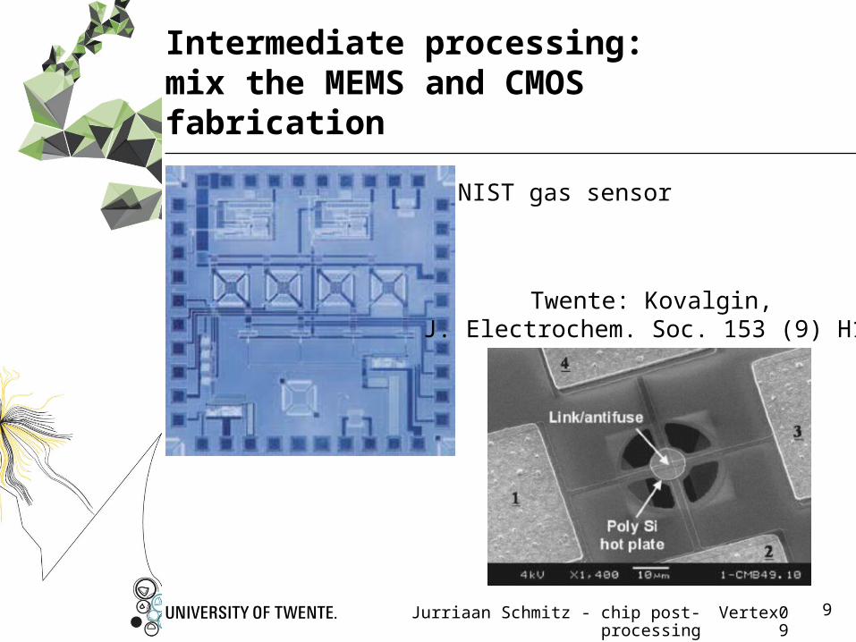
Intermediate processing:mix the MEMS and CMOS fabrication
NIST gas sensor
Twente: Kovalgin, J. Electrochem. Soc. 153 (9) H181

Vertex09Jurriaan Schmitz - chip post-processing 10
Wafer post-processing
a. Chip fabrication
b. Wafer dicing

Vertex09Jurriaan Schmitz - chip post-processing 11
Wafer post-processing
a. Chip fabrication
b. Post-processing
c. Wafer dicing

Vertex09Jurriaan Schmitz - chip post-processing 12
Logistics
Chip fabrication: standard, at any regular (CMOS) fab
Post-processing: special,in a custom CR laboratory
Wafer dicing, packaging: specialized work like MEMS packaging, e.g. Amkor, Boschman
a. Chip fabrication
b. Post-processing
c. Wafer dicing

Vertex09Jurriaan Schmitz - chip post-processing 13
Pros and cons
We do not interfere with the (CMOS) fab process
We can buy good quality chips
We can use any lab for this
Excellent alignment and contacts
Cheap mass-manufacturing
We must keep the CMOS intact
We have to think the final stages through very carefully! (Standard solutions may fail)
a. Chip fabrication
b. Post-processing
c. Wafer dicing

Vertex09Jurriaan Schmitz - chip post-processing 14
Outline
The concept of wafer post-processing Successes of wafer post-processing
Active pixel sensors LCoS Digital MicroMirrors
Recent results Perspective for radiation imaging
Vertex09Jurriaan Schmitz - chip post-processing 15
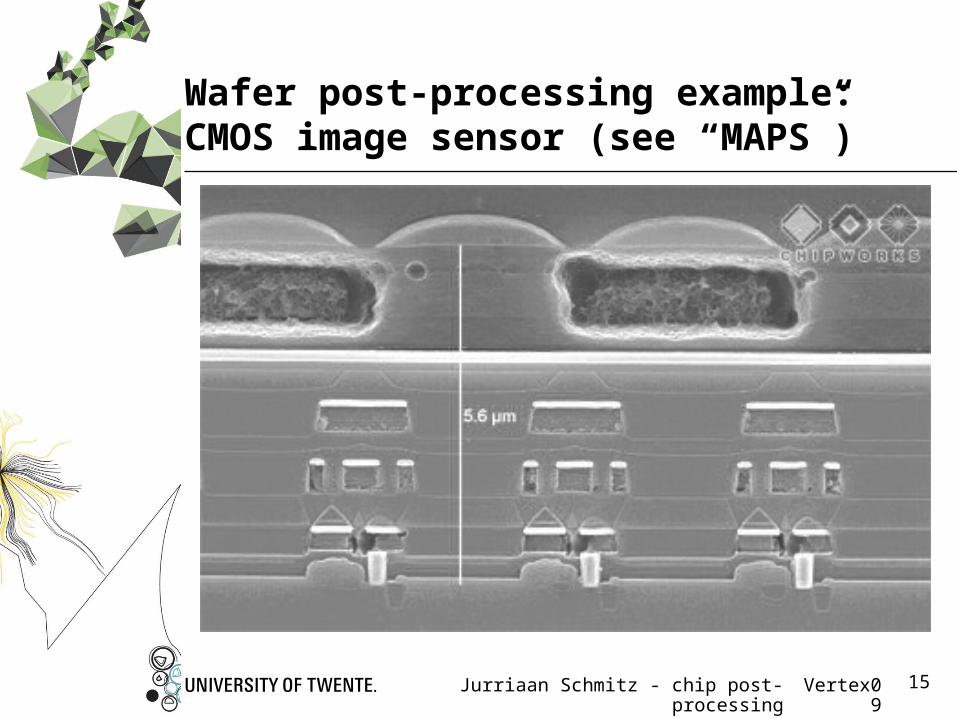
Wafer post-processing example: CMOS image sensor (see “MAPS”)
Vertex09Jurriaan Schmitz - chip post-processing 16
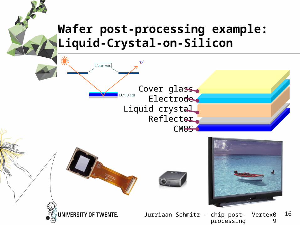
Wafer post-processing example: Liquid-Crystal-on-Silicon
Cover glassElectrode
Liquid crystalReflector
CMOS

Vertex09Jurriaan Schmitz - chip post-processing 17
Wafer post-processing example: Digital MicroMirror™

Vertex09Jurriaan Schmitz - chip post-processing 18

Vertex09Jurriaan Schmitz - chip post-processing 19
Outline
The concept of wafer post-processing Successes of wafer post-processing Recent results
Micromechanical structures Photodetectors 3D electronics
Perspective for radiation imaging

Vertex09Jurriaan Schmitz - chip post-processing 20
UC Berkeley: SiGe Resonator on top of CMOS

Vertex09Jurriaan Schmitz - chip post-processing 21
Example: silicon photodiodes on top of CMOSCEA-LETI, IEDM 2006

Vertex09Jurriaan Schmitz - chip post-processing 22
Rohm corp.: CIGS image sensor on CMOSIEDM 2008

Vertex09Jurriaan Schmitz - chip post-processing 23
CMOS on top of CMOS! (3D integration)
B. Rajendran et al., IEEE Trans. El. Dev. 54 (4) 707A. W. Topol et al.,
IBM J. Res. & Dev. 50 (4/5) 491
I. Brunets et al., IEEE Trans. El. Dev. 56 (8) 1637

Vertex09Jurriaan Schmitz - chip post-processing 24
CMOS post-processing: game rules
Careful treatment of the underlying CMOS: Temperature ≤ 450 °C Mild (or no) plasmas Maintain the H balance in the MOSFET Limited mechanical stress
The CMOS properties must remain unchanged:only then the standard infrastructure can be used.
Further reading:Jurriaan Schmitz, Nucl. Instr. Meth. A 576 (2007) 142.

Vertex09Jurriaan Schmitz - chip post-processing 25
Outline
The concept of wafer post-processing Successes of wafer post-processing Recent results Perspective for radiation imaging
MPGD: InGrid/GridPix Future

Vertex09Jurriaan Schmitz - chip post-processing 26
Bottleneck issues in radiation imaging
Power mgt. (cooling) Yield of interconnects (E/O)
System mass (rad. lengths)
What’s the answer?

Vertex09Jurriaan Schmitz - chip post-processing 27
Bottleneck issues in electronics
Power mgt. (cooling) Yield of interconnects
System mass
Solution in electronics:Integration and miniaturization

Vertex09Jurriaan Schmitz - chip post-processing 28
Radiation imaging – gaseous detectors
Cathodeplanes
Particle
Anodewires
Traditional MWPC InGrid

Vertex09Jurriaan Schmitz - chip post-processing 29
InGrid: Integrated Grid
Use an ASIC as read-out electronics Perfect alignment holes to pixels No dead areas Geometrical freedom No manual manufacturing
Pixel pad
Supporting pillar
Grid
Cathode
CMOS chip

Vertex09Jurriaan Schmitz - chip post-processing 30
The microsystem
Al membrane(-400-450 V)
SU-8 pillar(50 μm high)
a-Si protection
Medipix2 chip(or Timepix)

Vertex09Jurriaan Schmitz - chip post-processing 31
Process flow – suspended membrane
Deposit spark protection film:a-Si or Silicon-rich nitride
SU-8 photoresist for pillars
Al deposition is critical:unexposed SU-8 (yellow) should not crosslink
Al patterning also critical: lithography at room temperature to protect SU-8
Membrane release at end, after wafer dicing (fragility)
50 µm SU-8 coating and exposure
0.8 µm Al deposition + patterning
SU-8 development
Spark protection

Vertex09Jurriaan Schmitz - chip post-processing 32
The InGrid detector
2-D and 3-D mip-tracking shown Good energy resolution (11.7% FWHM for 55Fe in Ar/CH4)
Micromegas built on a chip, as well as GEM Multiple electrodes shown Beam tests for mip-tracking and transition radiation
Vertex09Jurriaan Schmitz - chip post-processing 33
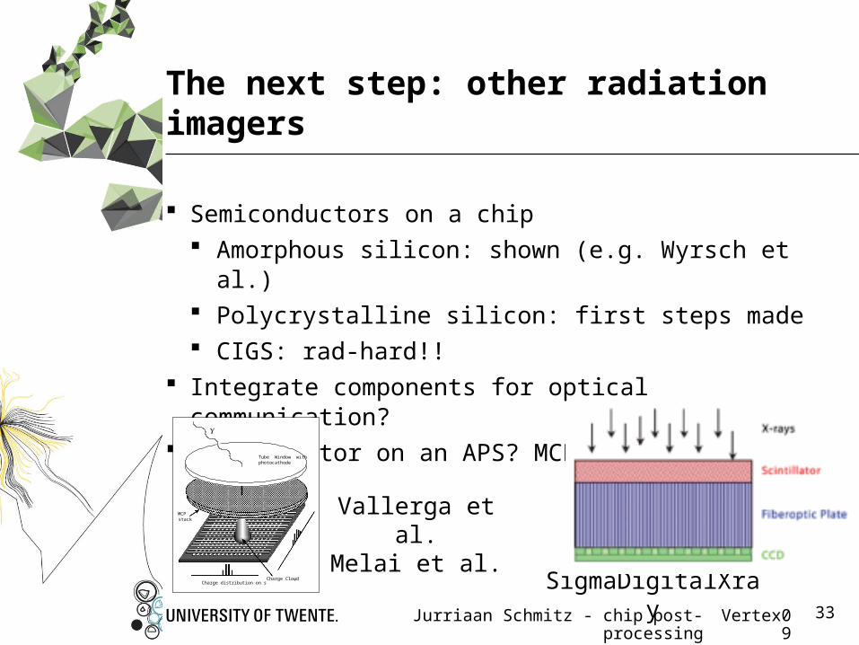
The next step: other radiation imagers
Semiconductors on a chip Amorphous silicon: shown (e.g. Wyrsch et al.) Polycrystalline silicon: first steps made CIGS: rad-hard!!
Integrate components for optical communication? Scintillator on an APS? MCP on a chip?
SigmaDigitalXray
Charge distribution on strips Charge Cloud
MCP stack
Tube Window with photocathode
Vallerga et al.
Melai et al.

Vertex09Jurriaan Schmitz - chip post-processing 34
Conclusions
What can we build on top of CMOS? Light projectors CMOS imagers More electronics Radiation imaging detectors …
There’s plenty of room at the top!
Vertex09Jurriaan Schmitz - chip post-processing 35
Thanks…
My low-temperature coworkers:
Tom Aarnink, Victor Blanco Carballo, Arjen Boogaard, Ihor Brunets, Jisk Holleman, Alexey Kovalgin, Jiwu Lu, Joost Melai, Cora Salm, Sander Smits, Rob Wolters, Yevgen Bilevych, Marten Bosma, Max Chefdeville, Harry van der Graaf, Martin Fransen, Jan Visschers, Jan Timmermans
Our sponsors:
The Dutch Technology Foundation, FOM
NXP Research, Adixen/Alcatel, ASM International
…and the Medipix consortium