Version :1 - scancraft View/PD024OX4 Ver 1_0.pdf · Built-in TCON corresponding to the image...
24
PD024OX4 The information contained herein is the exclusive property of Prime View International Co., Ltd. and shall not be distributed, reproduced, or disclosed in whole or in part without prior written permission of Prime View International Co., Ltd. Page 1 Version :1.0
Transcript of Version :1 - scancraft View/PD024OX4 Ver 1_0.pdf · Built-in TCON corresponding to the image...
PD024OX4
The information contained herein is the exclusive property of Prime View International Co., Ltd. and shall not be distributed, reproduced, or disclosed in whole or in part without prior written permission of Prime View International Co., Ltd. Page 1
Version :1.0

PD024OX4
The information contained herein is the exclusive property of Prime View International Co., Ltd. and shall not be distributed, reproduced, or disclosed in whole or in part without prior written permission of Prime View International Co., Ltd. Page 2
TECHNICAL SPECIFICATION
CONTENTS
NO. ITEM PAGE - Cover 1
- Contents 2
1 Application 3
2 Features 3
3 Mechanical Specifications 3
4 Mechanical Drawing of TFT-LCD Module 4
5 Input / Output Terminals 5 6 Absolute Maximum Ratings 7 7 Electrical Characteristics 7 8 Pixel Arrangement 8
9 Display Color and Gary Scale Reference 9
10 Block Diagram 10
11 Interface Timing 11
12 Power ON Sequence 16
13 Optical Characteristics 16
14 Handling Cautions 20
15 Reliability Test 21
16 Packing Diagram 22 - Revision History 24

PD024OX4
The information contained herein is the exclusive property of Prime View International Co., Ltd. and shall not be distributed, reproduced, or disclosed in whole or in part without prior written permission of Prime View International Co., Ltd. Page 3
1. Application
This technical specification applies to a 2.36” color TFT-LCD panel. This is designed for printer application and other electronic products which require high quality flat panel display.
2. Features
. Pixel in delta configuration
. Enables an approximately 16,190,000 color display by approximate 8-bit function.
. Provide a 3-wire clock synchronous serial interface for various operation mode settings.
. Built-in TCON corresponding to the image interface of the RGB form.
. Image reversion : Up/Down and Left/Right.
. Built-in control circuit for LED driving.
. Built-in power-save functions such as the stand-by mode.
. Built-in Vcom amplitude voltage output circuit.
3. Mechanical Specifications
Parameter Specifications Unit Screen Size 2.36 (diagonal) inch
Display Format 160×( RGB )×234 dot Display colors 262,144
Active Area 48.0(H)×35.685(V) mm Pixel Pitch 0.3(H)×0.4575 (V) mm
Pixel Configuration Delta Outline Dimension 55.2( W )×47.55 ( V ) ×2.9(D)(typ.) mm
Weight 12±1.5 g Back-light Three LED
Surface Treatment Anti – Glare Display model Normally white

PD024OX4
The information contained herein is the exclusive property of Prime View International Co., Ltd. and shall not be distributed, reproduced, or disclosed in whole or in part without prior written permission of Prime View International Co., Ltd. Page 4
4. Mechanical Drawing of TFT-LCD Module
P
I TA
PE
N
O B
EN
DIN
G A
REA
PD024OX4
The information contained herein is the exclusive property of Prime View International Co., Ltd. and shall not be distributed, reproduced, or disclosed in whole or in part without prior written permission of Prime View International Co., Ltd. Page 5
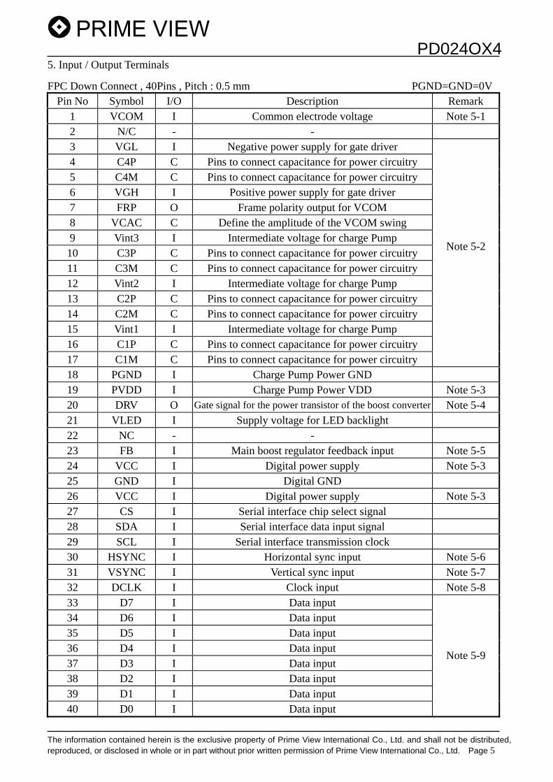
5. Input / Output Terminals FPC Down Connect , 40Pins , Pitch : 0.5 mm PGND=GND=0V
Pin No Symbol I/O Description Remark 1 VCOM I Common electrode voltage Note 5-1 2 N/C - - 3 VGL I Negative power supply for gate driver 4 C4P C Pins to connect capacitance for power circuitry 5 C4M C Pins to connect capacitance for power circuitry 6 VGH I Positive power supply for gate driver 7 FRP O Frame polarity output for VCOM 8 VCAC C Define the amplitude of the VCOM swing 9 Vint3 I Intermediate voltage for charge Pump 10 C3P C Pins to connect capacitance for power circuitry 11 C3M C Pins to connect capacitance for power circuitry 12 Vint2 I Intermediate voltage for charge Pump 13 C2P C Pins to connect capacitance for power circuitry 14 C2M C Pins to connect capacitance for power circuitry 15 Vint1 I Intermediate voltage for charge Pump 16 C1P C Pins to connect capacitance for power circuitry 17 C1M C Pins to connect capacitance for power circuitry
Note 5-2
18 PGND I Charge Pump Power GND 19 PVDD I Charge Pump Power VDD Note 5-3 20 DRV O Gate signal for the power transistor of the boost converter Note 5-4 21 VLED I Supply voltage for LED backlight 22 NC - - 23 FB I Main boost regulator feedback input Note 5-5 24 VCC I Digital power supply Note 5-3 25 GND I Digital GND 26 VCC I Digital power supply Note 5-3 27 CS I Serial interface chip select signal 28 SDA I Serial interface data input signal 29 SCL I Serial interface transmission clock 30 HSYNC I Horizontal sync input Note 5-6 31 VSYNC I Vertical sync input Note 5-7 32 DCLK I Clock input Note 5-8 33 D7 I Data input 34 D6 I Data input 35 D5 I Data input 36 D4 I Data input 37 D3 I Data input 38 D2 I Data input 39 D1 I Data input 40 D0 I Data input
Note 5-9

PD024OX4
The information contained herein is the exclusive property of Prime View International Co., Ltd. and shall not be distributed, reproduced, or disclosed in whole or in part without prior written permission of Prime View International Co., Ltd. Page 6
Note 5-1:VCOM = +5.0 Vp-p. (Typ.) Note 5-2: This is generated by the Step-up Circuit 1 and 2 , The external capacitor is required On those pins as following. Capacitor Capacity and Applied
voltage Recommended Breakdown
Remark
(C1)Vint2 1uF/Vint2 6V (C2)C1P/M 1uF/Vint2 6V ~ 10V (C3)Vint1 1uF/Vint1 10V (C4)C2P/M 1uF/Vint1 10V ~ 16V (C5)C3P/M 1uF/Vint1 10V ~ 25V (C6)VGH 1uF/VGH 25V (C7)VGL 1uF/VGL 25V (C8)Vint3 1uF/Vint3 10V (C9)VCAC 1uF/VCAC 10V (C10) FRP 1uF/FRP 10V
Note 5-3: PVDD, VCC = +3.3 V (Typ.) Note 5-4: Outputs the control signal of switching regulator for LED. Duty cycle varies according to FB input voltage. Note 5-5: Feedback signal of switching signal for LED. It controls DRV output duty cycle with 0.6V input level sense. Note 5-7: Horizontal sync signal, it is a “Low” active signal Note 5-8: Vertical sync signal, it is a “Low” active signal. Note 5-9: Dot clock signal for RGB interface, timing for data loading defined at rising edge.

PD024OX4
The information contained herein is the exclusive property of Prime View International Co., Ltd. and shall not be distributed, reproduced, or disclosed in whole or in part without prior written permission of Prime View International Co., Ltd. Page 7
6. Absolute Maximum Ratings The followings are maximum values, which if exceeded, may cause faulty operation or damage to the unit. PGND=GND=0V , Ta = 25℃
Parameter Symbol MIN. MAX. Unit Remark Vcc -0.3 4 V
Power Supply Voltage PVDD -0.3 4.6 V
Input Signal Voltage Vcom -0.5 5.2 V Digital Input Voltage VIN -0.3 Vcc+0.3 V Storage Temperature TST -20 70 oC Operation Temperature TOP 0 60 oC Maximum clock frequency Fmax 12 MHz 7. Electrical Characteristics 7-1 Operation condition PGND=GND=0V , Ta = 25℃
Parameter Symbol Min. Typ. Max. Unit Remark Supply Voltage for Source Driver Vcc 3.0 3.3 3.6
PVDD 3.0 3.3 3.6 V
H level VGH 14 15 16 V Note 7-1 Supply Voltage for Gate Driver L level VGL -9.5 -8 -6.5 V Note 7-1
H level VIH 0.7 VCC - VCC V Digital input voltage
L level VIL 0 - 0.3 VCC V
H level VOH 0.7 VCC - VCC V Digital output voltage
L level VOL 0 - 0.3 VCC V
VCOM AC - +5.0 - VP-PAC Component of VCOMVCOM
VCOM DC - 1.5 - V Note 7-2 Note 7-1: VGH and VGL supplied by internal setup-up circuit. Note 7-2: PVI strongly suggests that the VCOM DC level shall be adjustable , and the adjustable level
range is 1.5±1V , every module’s VCOM DC level shall be carefully adjusted to show a best image performance.

PD024OX4
The information contained herein is the exclusive property of Prime View International Co., Ltd. and shall not be distributed, reproduced, or disclosed in whole or in part without prior written permission of Prime View International Co., Ltd. Page 8
7-2 Power consumption
Parameter Symbol Min TYP MAX Unit Remark Supply voltage of LED backlight VLED 9.0 10.0 11.5 V IL = 20 mA
Supply current of LED backlight ILED 20 mA Note 7-3 Backlight Power Consumption PLED 180 200 230 mW Note 7-4
Note 7-3: LED B/L applied information, please refer to the appendix at the end . Note 7-4: PLED = VLED* ILED.
GLEDVLED
Parameter Symbol Conditions TYP. MAX. Unit Remark
Supply current for source driver ICC VCC =+3.3V 6 7.5 mA Supply current for gate driver PVDD PVDD1=+3.3V 75 95 mA Total power consumption 267 338 W 8. Pixel arrangement and input pin connector No.
R GRBGRBG B
G BGRBGRB R
R GRBGRBG B
G BGRBGRB R
R GRBGRBG B
G BGRBGRB R
1 447947865432
1
234
233
4
3
2
80
40 1

PD024OX4
The information contained herein is the exclusive property of Prime View International Co., Ltd. and shall not be distributed, reproduced, or disclosed in whole or in part without prior written permission of Prime View International Co., Ltd. Page 9
9. Display Color and Gray Scale Reference
Input Color Data Color Red Green Blue
R5 R4 R3 R2 R1 R0 G5 G4 G3 G2 G1 G0 B5 B4 B3 B2 B1 B0 Black 0 0 0 0 0 0 0 0 0 0 0 0 0 0 0 0 0 0 Red (63) 1 1 1 1 1 1 0 0 0 0 0 0 0 0 0 0 0 0 Green (63) 0 0 0 0 0 0 1 1 1 1 1 1 0 0 0 0 0 0
Basic Blue (63) 0 0 0 0 0 0 0 0 0 0 0 0 1 1 1 1 1 1Colors Cyan 0 0 0 0 0 0 1 1 1 1 1 1 1 1 1 1 1 1
Magenta 1 1 1 1 1 1 0 0 0 0 0 0 1 1 1 1 1 1 Yellow 1 1 1 1 1 1 1 1 1 1 1 1 0 0 0 0 0 0 White 1 1 1 1 1 1 1 1 1 1 1 1 1 1 1 1 1 1 Red (00) 0 0 0 0 0 0 0 0 0 0 0 0 0 0 0 0 0 0 Red (01) 0 0 0 0 0 1 0 0 0 0 0 0 0 0 0 0 0 0 Red (02) 0 0 0 0 1 0 0 0 0 0 0 0 0 0 0 0 0 0 Darker
Red ↓ ↓ ↓ ↓ ↓ ↓ ↓ ↓ ↓ ↓ ↓ ↓ ↓ ↓ ↓ ↓ ↓ ↓ ↓ Brighter Red (61) 1 1 1 1 0 1 0 0 0 0 0 0 0 0 0 0 0 0 Red (62) 1 1 1 1 1 0 0 0 0 0 0 0 0 0 0 0 0 0 Red (63) 1 1 1 1 1 1 0 0 0 0 0 0 0 0 0 0 0 0 Green (00) 0 0 0 0 0 0 0 0 0 0 0 0 0 0 0 0 0 0 Green (01) 0 0 0 0 0 0 0 0 0 0 0 1 0 0 0 0 0 0 Green (02) 0 0 0 0 0 0 0 0 0 0 1 0 0 0 0 0 0 0 Darker
Green ↓ ↓ ↓ ↓ ↓ ↓ ↓ ↓ ↓ ↓ ↓ ↓ ↓ ↓ ↓ ↓ ↓ ↓ ↓ Brighter Green (61) 0 0 0 0 0 0 1 1 1 1 0 1 0 0 0 0 0 0 Green (62) 0 0 0 0 0 0 1 1 1 1 1 0 0 0 0 0 0 0 Green (63) 0 0 0 0 0 0 1 1 1 1 1 1 0 0 0 0 0 0 Blue (00) 0 0 0 0 0 0 0 0 0 0 0 0 0 0 0 0 0 0 Blue (01) 0 0 0 0 0 0 0 0 0 0 0 0 0 0 0 0 0 1 Blue (02) 0 0 0 0 0 0 0 0 0 0 0 0 0 0 0 0 1 0 Darker
Blue ↓ ↓ ↓ ↓ ↓ ↓ ↓ ↓ ↓ ↓ ↓ ↓ ↓ ↓ ↓ ↓ ↓ ↓ ↓ Brighter Blue (61) 0 0 0 0 0 0 0 0 0 0 0 0 1 1 1 1 0 1 Blue (62) 0 0 0 0 0 0 0 0 0 0 0 0 1 1 1 1 1 0 Blue (63) 0 0 0 0 0 0 0 0 0 0 0 0 1 1 1 1 1 1

PD024OX4
The information contained herein is the exclusive property of Prime View International Co., Ltd. and shall not be distributed, reproduced, or disclosed in whole or in part without prior written permission of Prime View International Co., Ltd. Page 10
10. Block Diagram
LCD-Panel
Source DriverGate driver
PVDD C*MC*P Vcc HSYNCVSYNCDCLK
D0l
D7
CSSCLSDA
FB DRV

PD024OX4
The information contained herein is the exclusive property of Prime View International Co., Ltd. and shall not be distributed, reproduced, or disclosed in whole or in part without prior written permission of Prime View International Co., Ltd. Page 11
11. Interface Timing 11-1) Horizontal timing
Item Symbol Min. Typ. Max. Unit Remark Clock cycle time Trate 83.3 100 - ns
Clock low level pulse width Tcwl 15 - - ns Clock high level pulse width Tcwh 15 - - ns
Data setup Tds 12 - - ns Data hold Tdh 12 - - ns
- 63.5 - us HSYNC period Th - 635 - CLK H front porch Thf 5 11 - CLK
HSYNC low level pulse width Thp 4 44 - CLK H back porch Thb 83 100 114 CLK DCLK setup Tdcs 12 - - ns DCLK hold Tdch 12 - - ns
H valid display period Thd - 480 - CLK 11-2)Vertical timing
Item Symbol Min. Typ. Max. Unit Remark - 16.67 - ms VSYNC period Tv - 262 - HSYNC
V valid display period Tvd - 240 - HSYNC V front porch Tvf - 6 - HSYNC
VSYNC low level pulse width Tvp - 9 - HSYNC V back porch Tvb 5 16 19 HSYNC
11-3)Serial interface timing
Item Symbol Min. Typ. Max. Unit Remark Clock cycle time Tcycs 320 - - ns
Clock low level pulse width Tscwl 120 - - ns Clock high level pulse width Tscwh 120 - - ns
Data setup Tsds 120 - - ns Data hold Tsdh 120 - - ns
Chip select setup Tcss 120 - - ns Chip select hold Tcsh 120 - - ns

PD024OX4
The information contained herein is the exclusive property of Prime View International Co., Ltd. and shall not be distributed, reproduced, or disclosed in whole or in part without prior written permission of Prime View International Co., Ltd. Page 12
11-4)Timing Chart (a) Horizontal timing
DCLK
TrateTcwh
DCLK
Tds Tdh
Tcwl
HSYNC
DCLK
D0-7 INVALID VALID
1 2 479 480Tdcs
Thp
Tdch
Thb Thd Thf
Th
(b) Vertical timing
D0-7
DCLK
VSYNC
INVALID VALID VALID INVALID
HSYNC
1HSYNC Thp
1 2
Tvb Tvd Tvf
Tvp
Tv (c) Serial interface
SDA
SCL
CS
1 5432 9876 10 161514131211
D15 D13D14 D11D12 D10 D9 D8 D5D6D7 D2 D1 D0D3D4
0.3Vcc
0.7Vcc0.3Vcc
0.7Vcc
Tcss Tcycs Tscwh Tscwl
0.3Vcc
0.7Vcc
0.3Vcc
Tcsh
Tsds Tsdh

PD024OX4
The information contained herein is the exclusive property of Prime View International Co., Ltd. and shall not be distributed, reproduced, or disclosed in whole or in part without prior written permission of Prime View International Co., Ltd. Page 13
11-5) Internal Register Description and Timing Characteristics11-5) (a) List of register instructions
Address Data Register
No. D15 D14 D13 D12 D11 D10 D9 D8 D7 D6 D5 D4 D3 D2 D1 D0 R00h 0 0 0 0 - - - - - - - - SORST STB LEDON DCONR01h 0 0 1 0 0 0 0 - - - - - - EDZ - - R02h 0 1 0 0 - - - - - - - - MPOL - UD RL R03h 0 1 1 0 - - - - - - - - - - - - R04h 1 0 0 0 0 0 0 - - - - HBP4 HBP3 HBP2 HBP1 - R05h 1 0 1 0 - - - - - - - - VBP3 - VBP1 VBP0R06h 1 1 0 0 - - - - - - - - - - - - R07h 1 1 1 0 - - - - - - - - - - - -
“ – “ means don’t care
(b) Register function description * R00h (system control)
Address Data Register No. D15 D14 D13 D12 D11 D10 D9 D8 D7 D6 D5 D4 D3 D2 D1 D0
R00h 0 0 0 0 - - - - - - - - SORST STB LEDON DCONDefault 1 1 0 1
SORST: Used for system reset. System reset starts when SORST =”0”, and all instruction setting to default . STB: The standby mode turned on when STB =”0”, Display operation is off in standby mode. LEDON: This controls the on/off of the DRV signal for LED BL, the DRV output level becomes GND when LEDON =”0”. DCON: This controls the generator start/stop of the step-up clock DCCLK. The DCCLK generator starts when DCON =”1”. * R01h (Data control)
Address Data Register No. D15 D14 D13 D12 D11 D10 D9 D8 D7 D6 D5 D4 D3 D2 D1 D0
R01h 0 0 1 0 0 0 0 - - - - - - EDZ - - Default 0
EDZ: When EDZ =”0”, approximate 8-bit is implemented. Data input pin D0 and D1 must fixed to GND or VCC level when EDZ =”1”.

PD024OX4
The information contained herein is the exclusive property of Prime View International Co., Ltd. and shall not be distributed, reproduced, or disclosed in whole or in part without prior written permission of Prime View International Co., Ltd. Page 14
* R02h (Data control)
Address Data Register No. D15 D14 D13 D12 D11 D10 D9 D8 D7 D6 D5 D4 D3 D2 D1 D0
R02h 0 1 0 0 - - - - - - - - MPOL - UD RL Default 0 1 1
MPOL: Reverse the polarity of FRP output when MPOL = “1”.
U/D = 1, R/L = 1 U/D = 0, R/L = 0
* R04h (Timing control)
Address Data Register No. D15 D14 D13 D12 D11 D10 D9 D8 D7 D6 D5 D4 D3 D2 D1 D0
R04h 1 0 0 0 0 0 0 - - - - HBP4 HBP3 HBP2 HBP1 - Default 0 0 0 0
HBP4 HBP3 HBP2 HBP1 Horizontal back porch(Thb)
0 0 0 0 100DCLK 0 0 0 1 102DCLK 0 0 1 0 104DCLK 0 0 1 1 106DCLK 0 1 0 0 108DCLK 0 1 0 1 110DCLK 0 1 1 0 112DCLK 0 1 1 1 114DCLK 1 0 0 0 97DCLK 1 0 0 1 95DCLK 1 0 1 0 93DCLK 1 0 1 1 91DCLK 1 1 0 0 89DCLK 1 1 0 1 87DCLK 1 1 1 0 85DCLK 1 1 1 1 83DCLK

PD024OX4
The information contained herein is the exclusive property of Prime View International Co., Ltd. and shall not be distributed, reproduced, or disclosed in whole or in part without prior written permission of Prime View International Co., Ltd. Page 15
* R05h (Data control)
Address Data Register No. D15 D14 D13 D12 D11 D10 D9 D8 D7 D6 D5 D4 D3 D2 D1 D0
R05h 1 0 1 0 - - - - - - - - VBP3 - VBP1 VBP0Default 0 - 0 0
VBP3 VBP1 VBP0 Vertical back porch(Tvb)
0 0 0 16 HSYNC 0 0 1 17 HSYNC 0 1 0 18 HSYNC 0 1 1 19 HSYNC 1 0 0 8 HSYNC 1 0 1 7 HSYNC 1 1 0 6 HSYNC 1 1 1 5 HSYNC
11-6) Timing characters of serial interface Data loaded starting from the falling edge of CS input, ends at the rising edge. Data is on a 16bits basis. If an SCL of 16bits or more is not inputted during the CS “Low period”, transmitted data becomes invalid, as the data is not loaded inside. The register setting value after the data transmission is available in the next frame(after VSYNC input).
CS
SDA
SCL
Transfer strat Transfer end
D15 D14 D11D12D13 D10 D9 D8 D7 D5 D4 D1D3 D2D6 D0
Index Code Instruction data

PD024OX4
The information contained herein is the exclusive property of Prime View International Co., Ltd. and shall not be distributed, reproduced, or disclosed in whole or in part without prior written permission of Prime View International Co., Ltd. Page 16
12. Power On Sequence
VSS(0V)
VGG
ONOFF OFF
VDD1,VCC
VEE
T1
T2
T3
T4
Logic signalRGB-Video signal
VDD2
0 10ms≦T1<T2 2. 0ms<T3≦T4≦10ms 13.Optical Characteristics 13-1 Specification Ta = 25℃
Parameter Symbol Condition MIN. TYP. MAX. Unit RemarksHorizontal θ21, θ22 45 50 --- deg
θ11 30 35 --- deg Viewing Angle Vertical
θ12 CR≧10
10 15 --- deg Note 13-1
Contrast Ratio CR At optimizedViewing angle 200 400 --- Note 13-2
Rise Tr --- 6 12 ms Response time Fall Tf θ=0° --- 15 30 ms Note 13-3
Uniformity U 70 75 % Note 13-4
Brightness L 200 250 cd/㎡ Note 13-5X θ=0° 0.31 White
Chromaticity y θ=0° 0.33 Note 13-5
LED Life Time 10000 hrs Note13-6

PD024OX4
The information contained herein is the exclusive property of Prime View International Co., Ltd. and shall not be distributed, reproduced, or disclosed in whole or in part without prior written permission of Prime View International Co., Ltd. Page 17
Note 13-1 : The definitions of viewing angles
Luminance when Testing point is WhiteNote 13-2 : CR = Luminance when Testing point is Black Contrast ratio is measured in optimum common electrode voltage. Note 13-3 : The definition of response time :
100% 90%
10%
0%
White White
Brightness
Black
Tr Tf

PD024OX4
The information contained herein is the exclusive property of Prime View International Co., Ltd. and shall not be distributed, reproduced, or disclosed in whole or in part without prior written permission of Prime View International Co., Ltd. Page 18
Note 13-4 : The uniformity of LCD is defined as
The Minimum Brightness of the 9 testing PointsU = The Maximum Brightness of the 9 testing Points
Luminance meter : BM-7 fast (TOPCON) Measurement distance : 500 mm +/- 50 mm Ambient illumination : < 1 Lux Measuring direction : Perpendicular to the surface of module
The test pattern is white
1/6
1/6
2 /6
2 /6
1/6 1/62/6 2 /6 Note 13-5 : Topcon BM-7(fast) luminance meter 1.0° field of view is used in the testing (use PVI
backlight after 5 minutes operating), ILED = 20mA.
Note 13-6 : Constant current 20mA for each loop , and the center brightness must more than 50% of initial brightness value .

PD024OX4
The information contained herein is the exclusive property of Prime View International Co., Ltd. and shall not be distributed, reproduced, or disclosed in whole or in part without prior written permission of Prime View International Co., Ltd. Page 19
13-2 Testing configuration
LCD Display
R, G, B Waveform of Pattern A at Testing Point
R, G, B Waveform of Pattern B at Testing Point
500mm
BM-7(fast)
LCD
Backlight
R,G,B signalPattern
generator
input
Pattern A Pattern B
Testing Point Testing Point
63.6μs 63.6μs
63.6μs 63.6μs
Caution: 1. Environmental illumination≦1 lux 2. Before test CR, Vcom voltage must
be adjusted carefully to get the bestCR.
VcomRGBwaveform
RGBwaveform
Vcom
Vb=5.0V +/- 0.2V
Vw=1.3V +/- 0.2V

PD024OX4
The information contained herein is the exclusive property of Prime View International Co., Ltd. and shall not be distributed, reproduced, or disclosed in whole or in part without prior written permission of Prime View International Co., Ltd. Page 20
14. Handling Cautions 11-1) Mounting of module
a) Please power off the module when you connect the input/output connector. b) Please connect the ground surely. If the connection is not perfect, some following
problems may happen possibly. 1.The noise from the backlight unit will increase. 2.In some cases a part of module will heat.
c) Polarizer which is made of soft material and susceptible to flaw must be handled carefully. d) Protective film (Laminator) is applied on surface to protect it against scratches and dirt. It is recommended to peel off the laminator before use and taking care of static electricity. 11-2) Precautions in mounting a) Wipe off water drops or finger grease immediately. Long contact with water may cause discoloration or spots. b) TFT-LCD module uses glass which breaks or cracks easily if dropped or bumped on hard surface. Please handle with care. c) Since CMOS LSI is used in the module. So take care of static electricity and earth yourself when handling.
11-3) Others a) Do not expose the module to direct sunlight or intensive ultraviolet rays for many
hours. b) Store the module at a room temperature place. c) The voltage of beginning electric discharge may over the normal voltage because of leakage current from approach conductor by to draw lump read lead line around. d) If LCD panel breaks, it is possibly that the liquid crystal escapes from the panel. Avoid putting it into eyes or mouth. When liquid crystal sticks on hands, clothes or feet. Wash it out immediately with soap. e) Observe all other precautionary requirements in handling general electronic components.

PD024OX4
The information contained herein is the exclusive property of Prime View International Co., Ltd. and shall not be distributed, reproduced, or disclosed in whole or in part without prior written permission of Prime View International Co., Ltd. Page 21
15. Reliability Test
No. Test Item Test Condition 1 High Temperature Storage Test Ta = +70℃ , 240 hrs 2 Low Temperature Storage Test Ta = -20℃ , 240 hrs 3 High Temperature Operation Test Ta = 60℃ , 240 hrs 4 Low Temperature Operation Test Ta = 0℃ , 240 hrs
5 High Temperature & High Humidity Operation Test Ta = +60℃ , 90%RH , 240 hrs
6 Thermal Cycling Test (non-operating)
-20℃ → +70℃, 200 Cycles 30 min 30 min
7 Vibration Test (non-operating)
Frequency : 10 ~ 55 HZAmplitude : 1.0 mm
Sweep time : 11 mins Test Period : 6 Cycles for each direction of X, Y, Z
8 Shock Test (non-operating)
100G , 6ms Direction : ±X , ±Y , ±Z
Cycle : 3 times
9 Electrostatic Discharge Test (non-operating)
200pF , 0Ω ±200V
1 time / each terminal Ta: ambient temperature Note : The protective film must be removed before temperature test.
[Criteria] Under the display quality test conditions with normal operation state, there should be no change which may affect practical display function.

PD024OX4
The information contained herein is the exclusive property of Prime View International Co., Ltd. and shall not be distributed, reproduced, or disclosed in whole or in part without prior written permission of Prime View International Co., Ltd. Page 22
16. Packing Diagram

PD024OX4
The information contained herein is the exclusive property of Prime View International Co., Ltd. and shall not be distributed, reproduced, or disclosed in whole or in part without prior written permission of Prime View International Co., Ltd. Page 23

PD024OX4
The information contained herein is the exclusive property of Prime View International Co., Ltd. and shall not be distributed, reproduced, or disclosed in whole or in part without prior written permission of Prime View International Co., Ltd. Page 24
Revision History
Rev. Issued Date Revised Contents 0.1 Jan. 03, 2005 Preliminary
0.2 May. 15, 2005 Modify Page 10: R05h (VBP2 is fixed to high). Page 13: VSY change to Typ. 60Hz, and others relative parameters.
0.3 Jun. 15, 2005
Modify Page 03: Weight tolerance change to 15±1.5g. Page 06: Value of C1 P/M, C2 P/M, C3 P/M. Page 12: Add LED B/L power consumption. Page 15: Change Tr Typ. to 6ms; Tf Typ. to 15ms. Page 21: Add packing drawing.
0.4 Aug.19,2005
Modify
Page03: 3. Mechanical Specifications
Weight from 15±1.5g change to 12±1.5g. Page07: 7-1 Operation condition
VGH:From Min:14.5 Typ:15 Max:17.5 Change to Min:14 Typ:15 Max:16
VGL:From Min:-12 Typ:-10 Max:-9.4 Change to Min: -10.5Typ: -8.5 Max:-6.5
7-2 Power consumption
Supply current for gate driver:
From Typ:9 Max:12 Change to Typ:72 Max:90
Total power consumption:
From Typ:49.5 Max:66 Change to Typ:258 Max:324
Add
Page21: 15. Reliability Test
High Temperature Operation Test :Ta = 60℃ , 240 hrs
1.0 Sep.07,2005 NEW