Verilog 2 - Design Examples · L03-14 Verilog execution semantics - Confusing - Best solution is to...
15
L03-1 Verilog 2 - Design Examples •Modified by Michael Taylor from Arvind’s MIT 6.375 slides.
Transcript of Verilog 2 - Design Examples · L03-14 Verilog execution semantics - Confusing - Best solution is to...

L03-1
Verilog 2 - Design Examples
• Modified by Michael Taylor from Arvind’s MIT 6.375 slides.

L03-2
Verilog can be used at several levels
automatic tools to synthesize a low-level gate-level model
High-Level Behavioral
Register Transfer Level
Gate Level
A common approach is to use C/C++ for initial behavioral modeling, and for building test rigs

L03-3
Writing synthesizable Verilog Recap: Combinational logic " Use continuous assignments (assign)
assign C_in = B_out + 1;
" Use always_comb blocks with blocking assignments (=)
always_comb begin out = 2’d0; if (in1 == 1) out = 2’d1; else if (in2 == 1) out = 2’d2; end
" Every variable should have a default value to avoid inadvertent introduction of latches
" Don’t assign to same variable from more than one always_comb block. Race conditions in behavioral sim, synthesizes incorrectly.
always blocks allow more expressive control structures, though not all will synthesize
default value
L03-4
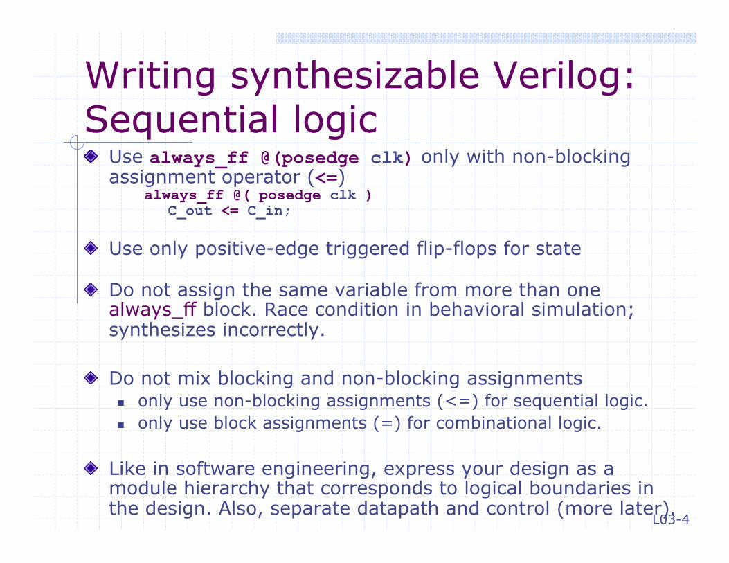
Writing synthesizable Verilog: Sequential logic " Use always_ff @(posedge clk) only with non-blocking
assignment operator (<=) always_ff @( posedge clk )
C_out <= C_in;
" Use only positive-edge triggered flip-flops for state
" Do not assign the same variable from more than one always_ff block. Race condition in behavioral simulation; synthesizes incorrectly.
" Do not mix blocking and non-blocking assignments only use non-blocking assignments (<=) for sequential logic. only use block assignments (=) for combinational logic.
" Like in software engineering, express your design as a module hierarchy that corresponds to logical boundaries in the design. Also, separate datapath and control (more later).

L03-5
wire A_next, B_next, C_next; reg A_r, B_r, C_r;
always_ff @( posedge clk ) begin A_r <= A_next; B_r <= B_next; C_r <= C_next; end
assign B_next = A_r + 1; assign C_next = B_r + 1;
An Example: Good Style
+1
A
+1
B C
Readable, combinational and sequential logic are separated.
Standard naming: A_r is the output of the register and A_next (or A_n) is the input.

L03-6
wire A_next; reg B_next, C_next; reg A_r, B_r, C_r;
always_ff @( posedge clk ) begin A_r <= A_next; B_r <= B_next; C_r <= C_next; end
always_comb begin B_next = A_r + 1; C_next = B_r + 1; end
An Example: Good Style
+1
A
+1
B C
Readable, combinational and sequential logic are separated.

L03-7
wire A_next, B_next, C_next; reg A_r, B_r, C_r;
always_ff @( posedge clk ) begin A_r <= A_next; B_r <= B_next; C_r <= C_next; assign B_next = A_r + 1; assign C_next = B_r + 1; end
Alternate implementation?
+1
A
+1
B C
Syntactically Incorrect.

L03-8
wire A_next; reg A_r, B_r, C_r;
always_ff @( posedge clk ) begin A_r <= A_next; B_r <= A_r + 1; C_r <= B_r + 1; end
An Example: Okay, but less readable?
+1
A
+1
B C
Is (B_r == A_next+1) ?
Nope - Why?
A_r <= A_next creates a register between A_next and A_r, not a wire.
L03-9
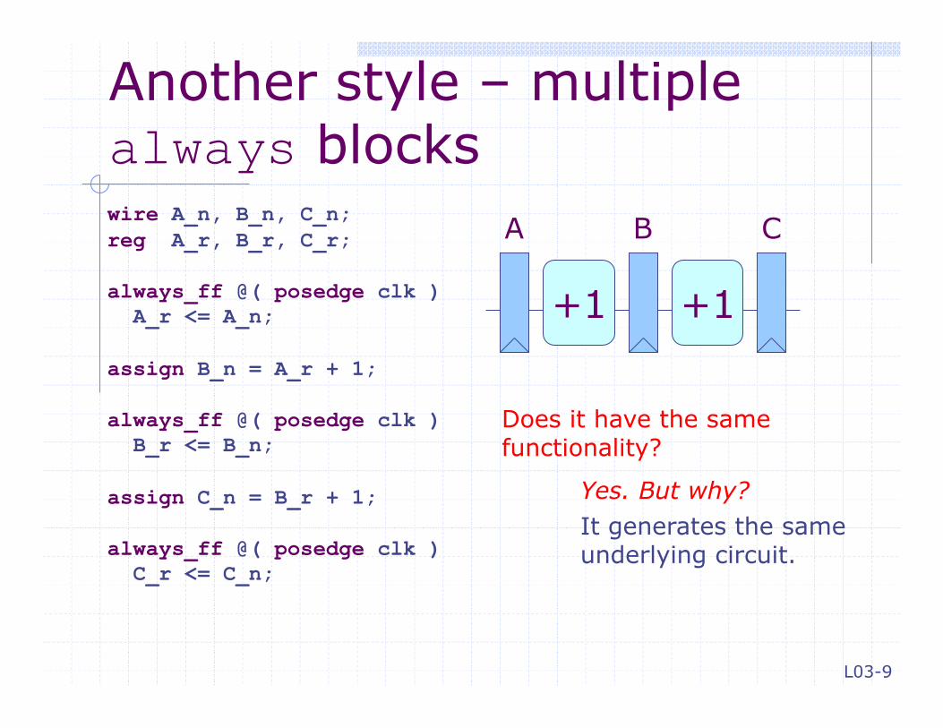
Another style – multiple always blocks wire A_n, B_n, C_n; reg A_r, B_r, C_r;
always_ff @( posedge clk ) A_r <= A_n;
assign B_n = A_r + 1;
always_ff @( posedge clk ) B_r <= B_n;
assign C_n = B_r + 1;
always_ff @( posedge clk ) C_r <= C_n;
+1
A
+1
B C
Does it have the same functionality?
It generates the same underlying circuit.
Yes. But why?

L03-10
wire A_n, B_n, C_n; reg A_r, B_r, C_r;
always @( posedge clk ) begin A_r = A_n; B_r = B_n; C_r = C_n; end
assign B_n = A_r + 1; assign C_n = B_r + 1;
How about this one?
+1
A
+1
B C
Will this synthesize?
Maybe
Is it correct?
No; Do not use “blocking assignments” in @posedge clk blocks. It is forbidden in this class.
L03-11
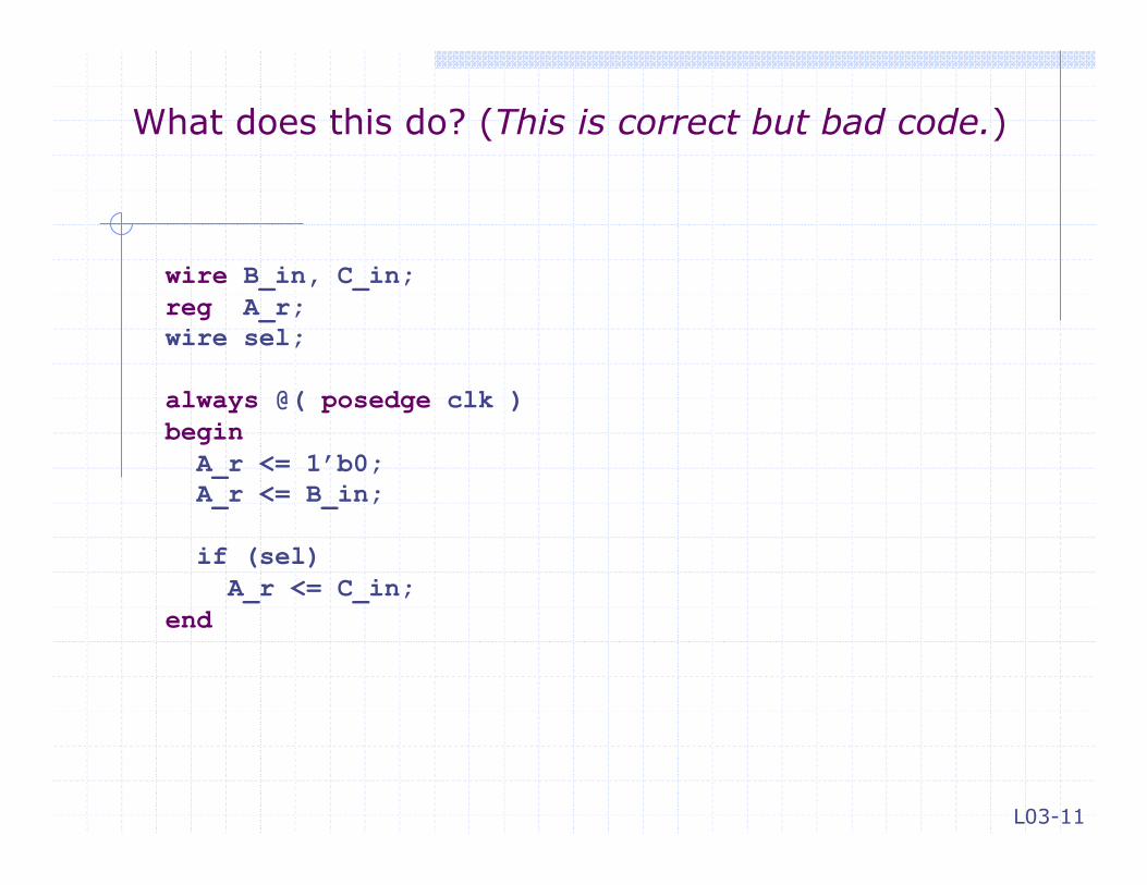
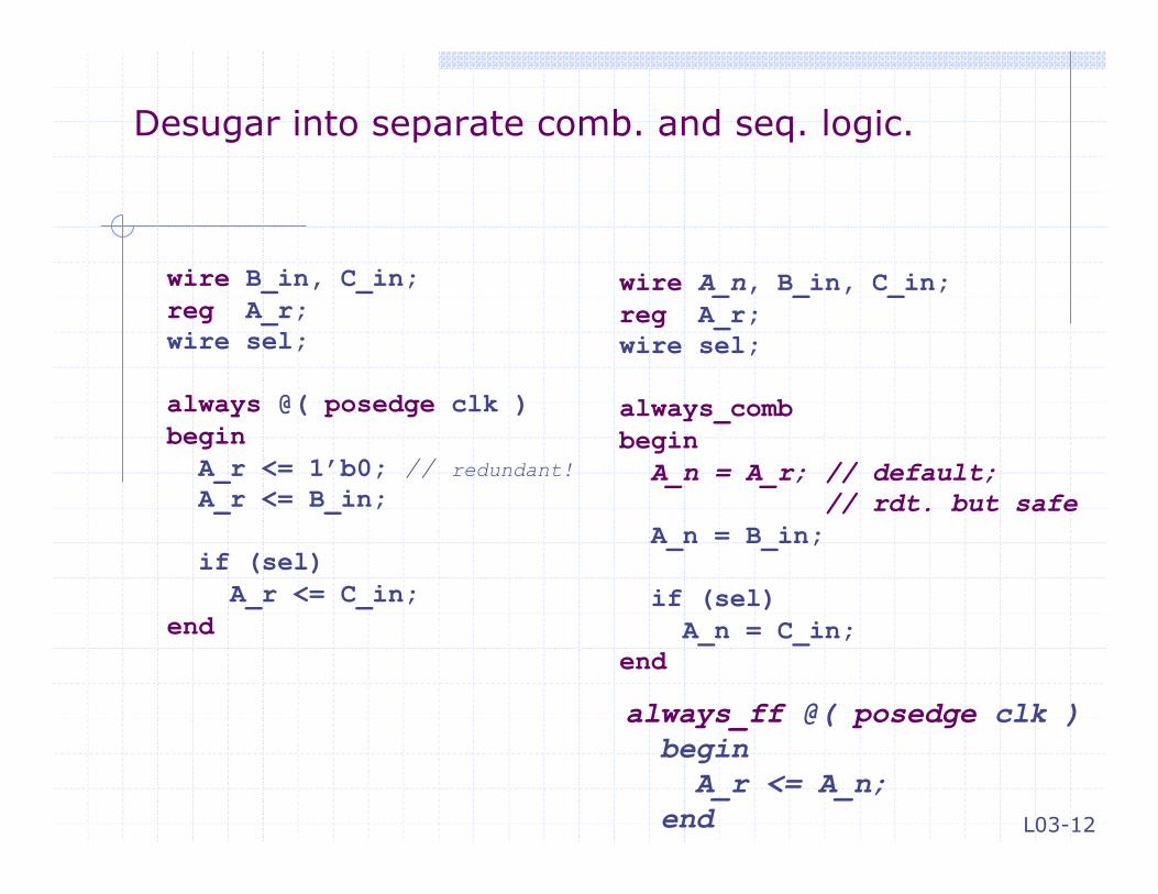
wire B_in, C_in; reg A_r; wire sel;
always @( posedge clk ) begin A_r <= 1’b0; A_r <= B_in;
if (sel) A_r <= C_in; end
What does this do? (This is correct but bad code.)
L03-12
Desugar into separate comb. and seq. logic.
wire B_in, C_in; reg A_r; wire sel;
always @( posedge clk ) begin A_r <= 1’b0; // redundant! A_r <= B_in;
if (sel) A_r <= C_in; end
wire A_n, B_in, C_in; reg A_r; wire sel;
always_comb begin A_n = A_r; // default; // rdt. but safe A_n = B_in;
if (sel) A_n = C_in; end
always_ff @( posedge clk ) begin A_r <= A_n; end

L03-13
What does this do? For each always_comb, assign, always_ff statement, draw the gates and wires.
wire A_n, B_in, C_in; reg A_r; wire choose;
always_comb begin A_n = A_r; // default
A_n = B_in;
if (choose) A_n = C_in; end
always_ff @( posedge clk ) begin A_r <= A_n; end
B_in
C_in
choose
• 0
• 1 A_n
A_r A_n

L03-14
Verilog execution semantics
- Confusing
- Best solution is to write synthesizable verilog that corresponds exactly to logic you have already designed on paper.
- Debugging is very difficult for Verilog. Don’t write code and “see if it works.” Test each “unknown” thing individually until you know what it does; then combine into larger entities.
- Before you try to simulate, manually check every wire to make sure that it is correctly (1) defined, connected to (2) source and (3) destination, and that (4) the logic driving it appears to be correct.
- This is way faster than finding the same bugs in the waveform viewer!

L03-15
Verilog struct example lab 2a examined this
typedef struct packed { logic [17-1:0] instr; logic [10-1:0] addr; } instr_packet_s;
instr_packet_s ip_n, ip_A_r, ip_B_r, ip_C_r;
assign ip_n = ‘{addr: addr_i , instr: instr_i};
assign { addr_o, instr_o } = { ip_C_r.addr, ip_C_r.instr };
always_ff @( posedge clk ) begin { ip_A_r, ip_B_r, ip_C_r } <= { ip_n, ip_A_r, ip_B_r }; end