Design, Analysis, and Verification of Moored Floating Caisson System
Verification of Floating-Point Adders
Yirng-An Chen Randal E. Bryant
April 1997
CMU-CS-98-121
School of Computer Science Carnegie Mellon University
Pittsburgh, PA 15213
Abstract
The floating-point division bug in Intel's Pentium processor and the overflow flag erratum of the FIST instruction in Intel's Pentium Pro and Pentium II processor have demonstrated the importance and the difficulty of verifying floating-point arithmetic circuits. In this paper, we present a "black box" version of verification of FP adders. In our approach, FP adders are verified by an extended word-level SMV using reusable specifications without knowing the circuit implementation. Word-level SMV is improved by using Multiplicative Power HDDs (*PHDDs), and by incorporating conditional symbolic simulation as well as a short-circuiting technique. Based on a case analysis, the adder specification is divided into several hundred implementation-independent sub-specifications. We applied our system and these specifications to verify the IEEE double precision FP adder in the Aurora III Chip from the University of Michigan. Our system found several design errors in this FP adder. Each specification can be checked in less than 5 minutes. A variant of the corrected FP adder was created to illustrate the ability of our system to handle different FP adder designs. For each adder, the verification task finished in 2 CPU hours on a Sun UltraSPARC-II server.
This research is sponsored by the Defense Advanced Research Projects Agency (DARPA) under contract number DABT63-96-C-0071.
The views and conclusions contained in this document are those of the authors and should not be interpreted as representing the official policies, either expressed or implied, of DARPA or the U.S. Goverment.
DISTRIBUTION STATEMENT A
Approved for public release; Distribution Unlimited
DTK! QUALITY lüurUy^u ö

Keywords: Binary Moment Diagram, *BMD, Hybrid Decision Diagram, HDD, K*BMD, Multiplicative Power Hybrid Decision Diagram, *PHDD, Arithmetic Circuit, Floating-Point Adder, IEEE Standard, Formal Verification

1 Introduction
The floating-point (FP) division bug [11, 22] in Intel's Pentium processor and the overflow flag erratum of the FIST instruction (floating-point to integer conversion) [14] in Intel's Pentium Pro and Pentium II processors have demonstrated the importance and the difficulty of verifying floating-point arithmetic circuits and the high cost of an arithmetic bug. FP adders are the most common units in floating-point processors. Modern high- speed FP adders [20,23] are very complicated, because they require many types of modules: a right shifter for alignment, a left shifter for normalization, a leading zero anticipator (LZA), an adder for mantissas, a rounding unit, etc. Exhaustive simulation or formal verification can be used to ensure the correctness of FP adders.
Most of the IEEE floating-point standard have been formalized by Carreno and Miner [5] in the HOL and PVS theoremprovers. Theoremprovers have been used to verify arithmetic circuits [18,21]. However, theorem provers require users to make use of detailed circuit knowledge and the verification process for floating-point circuits is very tedious. Another drawback of theorem provers is that the proofs are implementation-dependent.
After the famous Pentium division bug [11], Intel researchers applied word-level SMV [9] with Hybrid De- cision Diagrams (HDDs) [8] to verify the functionality of the floating-point unit in one of Intel's processors [7]. Due to the limitations of HDDs, the FP adder was partitioned into several sub-circuits whose specifications were expressed in terms of integer functions. Each sub-circuit was verified individually based on assumptions about its inputs. The correctness of the overall circuit had to be ascertained manually from the verified specifications of the sub-circuits. This partitioning approach is error prone, since mistakes could be introduced in any of the following steps: partitioning the circuit and the specification, performing case analysis for each sub-circuit, and proving the overall correctness of the circuit, which potentially could have used a theorem proven Moreover, their specifications are highly dependent on the circuit implementations.
The combination of model checking and theorem prover techniques was used to verify a IEEE double precision floating-point multiplier [1]. The circuit was partitioned into several sub-circuits which can be verified by model checking. The theorem prover handled the completeness of the proofs by inference rules to compose the verified specifications. This approach combines the strengths of both techniques. However, the proofs based on this approach are still implementation-dependent.
To the best of our knowledge, only two types of arithmetic circuits can be verified by treating them as black boxes (i.e., the specifications contain only the inputs and outputs). First, an integer adder can be verified by using Binary Decision Diagrams (BDDs) [2]. Second, Hamaguchi et al [15] presented the verification of integer multipliers without knowing their implementations using Multiplicative Binary Moment Diagrams (*BMDs) [4]. However, their approach does not work for incorrect designs, because the *BMDs explode in size and counterexamples can not be generated for debugging. None of the previous approaches can verify FP adders without knowing their circuit implementations.
In this paper, we present a black box version of verification of FP adders. In our approach, a FP adder is treated as a black box and is verified by an extended version of word-level SMV with reusable specifications. Word-level SMV is improved by using Multiplicative Power HDDs (*PHDDs) [6] to represent the FP func- tions, and by incorporating conditional symbolic simulation as well as a short-circuiting technique. The FP adder specification is divided into several hundred sub-specifications based on the sign bits and the exponent differences. These sub-specifications are implementation-independent, since they use only the input and output signals of FP adders.
The concept of conditional symbolic simulation is to perform the symbolic simulation of the circuit with some conditions to restrict the behavior of the circuit. This approach can be viewed as dynamically extracting circuit behavior under the given conditions without modifying the actual circuit. Can we verify the specifications of FP adders using conditional symbolic simulation, avoiding any use of circuit knowledge? We identify a conflict in variable orderings between the mantissa comparator and mantissa adder, which causes the BDD explosion
in conditional symbolic simulation. A short-circuiting technique to overcome this ordering conflict problem is presented and integrated into word-level SMV package. In general, this short-circuiting technique can be used when different parts of the circuit are used under different operating conditions.
We used our system and these specifications to verify the FP adder in the Aurora El Chip [16] at the University of Michigan. This FP adder is based on the design described in [20], and supports IEEE double precision and all 4 IEEE rounding modes. In this verification work, we verified the FP adder only in the round-to-nearest mode, because we believe that this is the most challenging rounding mode for verification. Our system found several design errors. Each specification can be checked in less than 3 minutes or 5 minutes including counterexample generation. A variant of the corrected FP adder was created and verified to illustrate the ability of our system to handle different FP adder designs. For each FP adder, verification took 2 CPU hours. We believe that our system and specifications can be applied to directly verify other FP adder designs and to help find design errors.
The overflow flag erratum of the FIST instruction (FP to integer conversion) [14] in Intel's Pentium Pro and Pentium II processors has illustrated the importance of verification of the conversion circuits which convert the data from one format to another format (e.g., IEEE single precision to double precision). Since these circuits are much simpler than FP adders and only have one input operand, we believe that our system can be used to verify the correctness of these circuits.
2 *PHDD Preliminary
For expressing functions from Boolean variables to integer values, BMDs[4] use the moment decomposition of a function:
/ = (1 -X) ■ fx + X- fx
= fx + X ■ (fx - fx)
- fx + X ■ fsx (1)
where •, + and - denote multiplication, addition and subtraction, respectively. Term fx (fx) denotes the positive (negative) cofactor of / with respect to variable x, i.e., the function resulting when the constant 1 (0) is substituted for x. By rearranging the terms, we obtained the third line of Equation 1. Here, f$x = fx - fx is called the linear moment of / with respect to x. This terminology arises by viewing / as a linear function with respect to its variables, and thus f$x is the partial derivative of / with respect to x. The negative cofactor fx will be termed the constant moment, i.e., it denotes the portion of function / that remains constant with respect to x. This decomposition is also called positive Davio in K*BMDs [13]. Each vertex of a BMD describes a function in terms of its moment decomposition with respect to the variable labeling the vertex. The two outgoing arcs denote the constant and linear moments of the function with respect to the variable.
Clarke, et cd. [8] extended BMDs to a form they call Hybrid Decision Diagrams (HDDs), where a function may be decomposed with respect to each variable in one of six decomposition types. In our experience with HDDs, we found that three of their six decomposition types are useful in the verification of arithmetic circuits. These three decomposition types are Shannon, Positive Davio, and Negative Davio. Therefore, Equation 1 is generalized to the following three equations according the variable's decomposition type:
/ = (1 — x) ■ fx + x ■ fx [Shannon) h + x • fsx (Positive Davio) (2) fx + (l- x) ■ fsx [Negative Davio)

Here, fsx = fa - fx is the partial derivative of / with respect to x. The BMD representation is a subset of HDDs. In other words, the HDD graph is the same as the BMD graph, if all of the variables use positive Davio decomposition.
Chen and Bryant [6] introduced multiplicative power-of-constant edge weights into HDDs to form a new representation called Multiplicative Power HDDs (*PHDDs). *PHDDs use three of HDD's six decompositions as expressed in Equation 2. Unlike the edge weights in *BMDs, the edge weights of *PHDDs are powers of a constant c. Thus, Equation 2 is rewritten as:
cw-((l-x)-fa + x-fa (wj) = { cw-{k + x-fSx)
CW ■ (fx + (1 - x) ■ fix)
(Shannon) (Positive Davio) (Negative Davio)
where (w, /) denotes cw x /. In general, the constant c can be any positive integer. Since the base value of the exponent in the IEEE floating-point (FP) format is 2, we will consider only c = 2 for the remainder of this paper. Observe that w can be negative, allowing representation of rational numbers. The power edge weights enable us to represent functions mapping Boolean variables to FP values without using rational numbers in our representation.
x y f 0 0 1 0 1 2 1 0 4 1 1 8
(a)
Figure 1: An integer function of Boolean variables, / = 1 + y + 3x + 3xy, is represented by (a) Truth table, (b) BMDs, (c) *BMDs, (d) HDDs with Shannon decompositions, (e) *PHDDs with Shannon decompositions. The dashed-edges are O-branches and the solid-edges are the 1-branches. The variables with Shannon and positive Davio decomposition types are drawn in the thin and thick vertices, respectively. The number i in the thin and thick boxes represents i and X, respectively.
Figure 1 shows an integer function / with Boolean variables x and y represented by a truth table, BMDs, *BMDs, and HDDs with Shannon decompositions (also called MTBDD [10]). In our drawing, the variables with Shannon and positive Davio decomposition types are drawn in thin and thick vertices, respectively. The number i in the thin and thick boxes represents i and X, respectively. A dashed line from a vertex with variable x points to the vertex represented function fa, fa, or fa for the Shannon, positive Davio or negative Davio decompositions, respectively. Similarly, a solid line from a vertex with variable x points to the vertex represented function fa, fax or fsx for the Shannon, positive Davio or negative Davio decompositions. Figure l.b shows the BMD representation. To construct this graph, we apply Equation 1 to function / recursively. First, with respect to variable x, we get fa = 1 + y, represented as the graph attached to the dashed-edge from vertex x, and fax = 3 + 3y, represented by the solid branch from vertex x. Observe that f$x can be expressed by 3 x fa. By extracting the factor 3 from fax, the graph becomes Figure I.e. This graph is called a Multiplicative BMD (*BMD), in which the greatest common divisor (GCD) is extracted from both branches. The edge weights

combine multiplicatively. The HDD with Shannon decompositions can be constructed from the truth table. The dashed branch of vertex x {fx) is constructed from the first two entries of the table, and the solid branch of vertex x (i.e., fx) is constructed from the last two entries of the table. Observe that fx is equal to 22 x fx. The *PHDDs can be constructed by extracting the powers-of-2 weights from the HDDs recursively.
Observe that if variables x and y are viewed as bits forming a 2-bit binary number, X=y+2x, then the function / can be rewritten as / = 2^y+2x'> = 2X. Observe that HDDs with Shannon decompositions and BMDs grow exponentially for this type of function. *BMDs can represent them efficiently due to edge weights. However, *BMDs and HDDs cannot represent the functions as / = 2X~B, where B is a constant, because they can only represent integer functions. *PHDDs can represent this type of functions efficiently by adding the edge weight of -B on the top the graph of 2X. Therefore, *PHDDs can represent the FP encoding and operations efficiently. Readers can refer to [6] for more details of FP representation using *PHDDs.
3 Floating-Point Adders
Let us consider the representation of FP numbers by IEEE standard 754. Double-precision FP numbers are stored in 64 bits: 1 bit for the sign (Sx), 11 bits for the exponent (Ex), and 52 bits for the mantissa (Nx). The exponent is a signed number represented with a bias (B) of 1023. The mantissa (Nx) represents a number less than 1. Based on the value of the exponent, the IEEE FP format can be divided into four cases:
(-1)5- xl.Nxx 2E'-B IfO<Ex< All 1 {normal) (-1)5* x 0.NX x 2X~B If Ex = 0 (denormal) NaN If Ex = Alll&Nx^0
(-1); ■ xoo // Ex = All 1 & Nx = 0 where NaN denotes Not-a-Number and oo represents infinity. Let Mx = \.NX or O.A^. Let m be the number of mantissa bits including the bit on the left of the binary point and n be number of exponent bits. For IEEE double precision, m=53 and n=ll.
Due to this encoding, an operation on two FP numbers cannot be rewritten as an arithmetic function of two inputs. For example, the addition of two FP numbers X (Sx, Ex, Mx) and Y (Sy, Ey, My) can not be expressed as X + Y, because of special cases when one of them is NaN or ±oo. Table 1 summarizes the
Y + —oo F +oo NaN
X —oo —oo —oo * NaN F —oo Round{X + Y) + 00 NaN
+oo * +oo +oo NaN NaN NaN NaN NaN NaN
Table 1: Summary of the FP addition of two numbers of X and Y. F represents the normal and denormal numbers. * indicates FP invalid arithmetic operands.
possible results of the FP addition of two numbers X and Y, where F represents a normalized or denormalized number. The result can be expressed as Round(X + Y) only when both operands have normal or denormal values. Otherwise, the result is determined by the case. When one operand is +oo and the other is — oo, the FP adder should raise the FP invalid arithmetic operand exception.
Figure 2.a shows the block diagram of the SNAP FP adder designed at Stanford University [20]. This adder was designed for fast operation based on the following facts. First, the alignment (right shift) and normalization (left shift) needed for addition are mutually exclusive. When a massive right shift is performed

during alignment, the massive left shift is not needed. On the other hand, the massive left shift is required only when the mantissa adder performs subtraction and the absolute value of exponent difference is less than 2 (i.e. no massive right shift). Second, the rounding can be performed by having the mantissa adder generate A + C, A + C + 1 and A + C + 2, where A and C are the inputs of the mantissa adder, and using the final multiplexor to chose the correct output.
* Sy
Exp. Select •*-
Sign Select
t=L Subtractor
MuxAbs
Path Select
Encode
in Exp. |^_
fset
Exp. Adjust
fy M
Swap * Sy
Right Shift & Sticky Bit
£U Mux
A C
Adder
LZA CRS
■ÖnesCampl
Left Shift
Fine Adjust
\ m Mux
Er Ey M, My
Exp. Select *-
Sign Select
I i~7in~~i 1 Subtractor Compare
MuxAbs
Path Select
Encode
Exp. Offset
Exp. Adjust
AC,
Swap
Right Shift & Sticky Bit
yj- Adder
GRS
Left Shift
Fine Adjust
\ ru Mux
A/„„
(a) (b)
Figure 2: The Stanford FP adder (a) and a variant (b).
In the exponent path, the exponent subtractor computes the difference of the exponents. The MuxAbs unit computes the absolute value of the difference for alignment. The larger exponent is selected as the input to the exponent adjust adder. During normalization, the mantissa may need a right shift, no shift or a massive left shift. The exponent adjust adder is prepared to handle all of these cases.
In the mantissa path, the operands are swapped as needed depending on the result of the exponent subtractor. The inputs to the mantissa adder are: the mantissa with larger exponent (A) and one of the three versions of the mantissa with small exponent (C): unshifted, right shifted by 1, and right shifted by many bits. The path select unit chooses the correct version of C based on the value of exponent difference. The version right shifted by many bits is provided by the right shifter, which also computes the information needed for the sticky bit. The mantissa adder performs the addition or subtraction of its two inputs depending on the signs of both operands and the operation (add or subtract). If the adder performs subtraction, the mantissa with smaller exponent will first be complemented. The adder generates all possible outcomes (A + C, A + C + 1, and A + C + 2) needed to obtain the final, normalized and rounded result. The A + C + 2 is required, because of the possible right shift

during normalization. For example, when the most significant bits of A and C are 1, A + C will have m +1 bits and must be right shifted by 1 bit. If the rounding logic decides to increase 1 in the least significant bit of the right shifted result, it means add 2 into A + C. When the operands have the same exponent and the operation of the mantissa adder is subtraction, the outputs of the adder could be negative. The ones complementer is used to adjust them to be positive. Then, one of these outputs is selected by the GRS unit to account for rounding. The GRS unit also computes the true guard (G), round(J?), sticky (5) bits and the bit to be left shifted into the result during normalization. When the operands are close (the exponent difference is 0,1, or -1) and the operation of the mantissa adder is subtraction, the result may need a massive left shift for normalization. The amount of left shift is predicted by the leading zero anticipator (LZ4) unit in parallel with the mantissa adder. The predicted amount may differ by one from the correct amount, but this 1 bit shift is made up by a \-bit fine adjust unit. Finally, one of the four possible results is selected to yield the final, rounded, and normalized result based on the outputs of the path select and GRS units.
Mx<My d
Ex=Ey
Er < Ev
Figure 3: Detail circuit of the compare unit
As an alternative to the SNAP design, the ones complementer after the mantissa adder can be avoided, if we ensure that input C of the mantissa adder is smaller than or equal to input A, when the exponent difference is 0 and the operation of mantissa adder is subtraction. To ensure this property, a mantissa comparator and extra circuits, as shown in [23], are needed to swap the mantissas correctly. Figure 2.b shows a variant of the SNAP FP adder with this modification (the compare unit is added and the ones complementer is deleted). This compare unit exists in many modern high-speed FP adder designs [23] and makes the verification harder described in Section 5.4. Figure 3 shows the detailed circuit of the compare unit which generates the signal to swap the mantissas. The signal Ex < Ey comes from the exponent subtracter. When Ex < Ey or Ex = Ey- and Mx < My (i.e., h =1), A is My (i.e. the mantissas are swapped). Otherwise, A is Mx.
4 Specifications of FP Adders
In this section, we focus on the general specifications of the FP adder, especially when both operands have denormal or normal values. For the cases in which at least one of operands is a NaN or oo, the specifications can be easily written at the bit level. For example, when both operands are NaN, the expected output is NaN (i.e. the exponent is all Is and the mantissa is not equal to zero). The specification can be expressed as the "AND" of the exponent output bits is 1 and the "OR" of the mantissa output bits is 1.
When both operands have normal or denormal values, the ideal specification is OUT — Round{X + Y). However, FP addition has exponential complexity with the word size of the exponent part for *PHDD. Thus, the specification must be divided into several sub-specifications for verification. According to the signs of both operands, the function X + Y can be rewritten as Equation 3.
X + Y = -1)' (2Ex~B X Mx + My X 2Ey~B) Sx = Sy (true addition)
(2 Ex—B X Mr My x 2^y Ey — B') Sx / Sy (true subtraction) (3)

Similarly, for FP subtraction, the function X - Y can be also rewritten as true addition when both operands have different signs and true subtraction when both operands have the same sign.
4.1 True Addition
Mr
Af„,
Mr
M„ M„
M„,
(a) Ex-E<m (b)Ex-Ey>=m
Figure 4: Cases of true addition for the mantissa part.
The *PHDDs for the true addition and subtraction still grow exponentially. Based on the sizes of the two exponents, the function X + Y for true addition can be rewritten as Equation 4.
X + Y = (-1) ■)EX-B
->EV-B x [Mx + (My » [Ex - Ey))) Ey<Ex
x {My + {MX» [Ey - Ex))) Ey > Ex (4)
When Ey < Ex, the exponent is Ex and the mantissa is the sum of Mx and My right shifted by (Ex - Ey) bits (i.e. My » (Ex - Ey) in the equation). Ex - Ey can range from 0 to 2n - 2, but the number of mantissa bits in FP format is only m bits. Figure 4 illustrates the possible cases of true addition for Ey < Ex based on the values of Ex - Ey. In Figure 4.a, for 0 < Ex - Ey < m, the intermediate (precise) result contains more than m bits. The right portion of the result contains L,G,R and S bits, where L is the least signification bit of the mantissa. The rounding mode will use these bits to perform the rounding and generate the final result(Moui) in m-bit format. When Ex - Ey > m as shown in Figure 4.b, the right shifted My only contributes to the intermediate result in the G, R and S bits. Depending the rounding mode, the output mantissa will be Mx or Mx +1 * 2_m+1. Therefore, we only need one specification in each rounding mode for the cases Ex-Ey > m. A similar analysis can be applied to the case Ey > Ex. Thus, the specifications for true addition with rounding can be written as:
m
men as:
' Cai[i\ =>• OUT = Round{{-\)s* x 2E*~B x (Mx + (My » i))) 0<i< Caz => OUT = Round{(-\)s* x 2E*~B x (Mx + (My » m))) i > m ~ r'n ^ OUT - Round{{-l)s* x 2^-ß x (My + (Mx » i))) 0 < i < m
OUT = Round((-l)s* x 2^-ß x (My + (Mx » m))) i > m C'a3[l\
(5)
where C0i[i], Ca2, Cai[i\ and Ca4 are the conditions Cond..add&Ex = Ey + i, CondjaddHz. Ex > Ey + m, Cond-add&Ey = Ex + i, and Cond-add&Ey > Ex + m, respectively. Cond.add represents the condition for true addition and exponent range (i.e. normal and denormal numbers only). OUT is composed from the outputs Sout, Eout and Mout. Conditions Ex- Ey = i and Ex- Ey> m are represented by 2Ex = 2E»+i and 2Ex > 2Ev+m. Both sets of variables must use Shannon decomposition to represent the FP function efficiently in [6]. With this decomposition, the graph sizes of Ex and Ey are exponential in *PHDDs, but 2Ex and 2Ey will have linear size. While building BDDs and *PHDDs for OUT from the circuit, the function on left side of =$■ will be used to simplify the BDDs automatically by conditional forward simulation.

The number of specifications for true addition is 2m + 1. For instance, the value of m for IEEE double precision is 53, thus the number of specifications for true addition is 107. Since the specifications are very similar to one another, they can be generated by a looping construct in word-level SMV.
4.2 True Subtraction
The specification for true subtraction can be divided into two cases: far{\Ex-Ey\ > 1) and close (Ex-Ey=0,l or -1). For the far case, the result of mantissa subtraction does not require a massive left shift (i.e., LZA is not active). Similar to the true addition, the specifications for true subtraction can be written as Equation 6.
C„i[i\ =>- OUT = Round{(-l)s* X 2E*~B X (Mx - [My » i))) 2<i<m Cs2 => OUT = Round((-l)s* x 2E-~B x (Mx - (My » m))) i > m Cs3[i]^OUT = Round{(-l)sy x2Ey~B x(My-(Mx»i))) 2<i<m Cs4 =» OUT = Round((-l)sy x lE*~B x (My - (Mx » m))) i > m
where Cs\ [i], Cs2, CS3 [i] and Cs4 are Condsub&Ex = Ey + i, Cond sub &EX > Ey + m, Condsub&Ey = Ex + i, and Condsub&Ey > Ex + m, respectively. Condsub represents the condition for true subtraction.
For the close case, the difference of the two mantissas may generate some leading zeroes such that normal- ization is required to product a result in IEEE format. For example, when Ex - Ey = 0, Mx - My=0.0...01 must be left shifted by m - 1 bits to 1.0...00. The number bits to left shift is computed in the LZA circuit and fed into the left shifter to perform normalization and into the subtracter to adjust the exponent. The number of bits to be left shifted ranges from 0 to m and is a function of Mx and My. The combination of left shifting and mantissa subtraction make the *PHDDs become irregular and grow exponentially. Therefore, the specifications for these cases must be divided further to take care of the exponential growth of *PHDD sizes.
Based on the number of leading zeroes in the intermediate result of mantissa subtraction, we divide the specifications for the true subtraction close case as shown in Equation 7.
Cci[t\ => OUT = Round{{-\)s- x 2E*~B x (Mx - (My » 1))) 0 < i < m Cc2[{\ =* OUT = Round({-\)sy x 2Ey-B x (My - (Mx » 1))) 0 < i < m Cc3[{\) => OUT = Round((-l)s* x 2E*~B x (Mx - My)) 1 < i < m cj[i\) => OUT = Round((-l)sy x 2Ey~B x (My - Mx)) 1 < i < m
(7)
where where Cc\[i\, Cc2[i\,Cci[i], and Cc4[f] are Condsub & Ex = Ey + 1 & LS[i\, Condsub &Ey = Ex + 1 & LS[i], Condsub&Ex = Ey&Mx > My & LS[i], and Condsub& Ey = Ex+ 1&MX < My & LS[i\, respectively. L S1 [i], LS2[i], L S 3 [i] and L 54 [i] represent the conditions that the intermediate result has i leading zeroes to be left shifted. LSl[i\, LS2[i\, LS3[i\ and LS4[i] are computed by 2m~{-1 < Mx - (My » 1) < 253-it2m-i-i < My-(MX » 1) < 2m~i,2m~i~1 <MX-My< 2m-l',and2m-2'-1 <My-Mx< 2m~l), respectively. A special case is that the output is zero when Ex is equal to Ey and Mx is equal to My. The specification is as follows: (Condsub &EX = Ey &MX = My) =^> OUT = 0.
4.3 Specification Coverage
Since the specifications of floating-point adders are split into several hundreds of sub-specifications, do these sub-specifications cover the entire input space? To answer this questions, someone would suggest to use theorem provers to handle the case splitting. In contrast, we propose a BDD approach to compute the coverage of our specifications.
Our approach is based on this observation that our specifications are in the form "cond =^> out = expectedjresult" and cond is only dependent on the inputs of the circuits. Thus, the union of the conds

of our specifications, which can be done by BDD operations, must be TRUE when our specifications cover the entire input space. In other words, the union of the conds can be used to compute the percentage of input space covered by our specifications and to generate the cases which are not covered by our specifications.
5 Verification System: Extended Word-Level SMV with *PHDDs
Model checking is a technique to determine which states satisfy a given temporal logic formula for a given state-transition graph. In SMV [19], BDDs are used to represent the transition relations and set of states. The model checking process is performed iteratively on these BDDs. SMV has been widely used to verify control circuits in industry, but for arithmetic circuits, particularly for ones containing multipliers, the BDDs grows too large to be tractable. Furthermore, expressing desired behavior with Boolean formulas are not appropriated.
To verify arithmetic circuits, word-level SMV [9] with HDDs extended SMV to handle word level expressions in the specification formulas. In word-level SMV, the transition relation as well as those formulas that do not involve words are represented using BDDs. HDDs are used only to compute word-level expressions such as addition and multiplication. When a relational operation is performed on two HDDs, a BDD is used to represent the set of assignments that satisfies the relation. The BDDs for temporal formulas are computed in the same way as in SMV. For example, the evaluation the formula AG(R = A + B), where R, A and B are word-level functions and AG is a temporal operator, is performed by first computing the HDDs for R, A, B and A + B, then generating BDDs for the relation R = A + B, and finally applying the AG operator to these BDDs. The reader can refer to [9] for the details of word-level SMV.
.., xn
Region 3
wr -'wo
Region 2
zk' >zo
Region 1
Figure 5: Horizontal division of a combinational circuit,
We have integrated *PHDDs into word-level SMV and introduced relational operators for floating-point numbers. As in word-level SMV, only the word-level functions are represented by *PHDDs and the rest of the functions are represented by BDDs.
Zhao's thesis [24] describes the layering backward substitution, a variant of Hamaguchi's backward sub- stitution approach [15], although the public released version of word-level SMV does not implement this feature. We have implemented this feature in our system. The main idea of layering backward substitution is to virtually cut the circuit horizontally by introducing auxiliary variables to avoid the explosion of BDDs while symbolic evaluating bit level circuits. Figure 5 shows a horizontal division of a combinational circuit with primary inputs xo,...,xm and outputs i/o,..., yn- For 0 < i < n, y,- = fi(xo,...,xm) where /; is a Boolean function, but it may not be feasible to be represented as a BDD. The circuit is divided into several

layers by declaring some of the internal nodes as auxiliary variables. In this example, y, = fu(zo,..., Zk); zt = f2i(w0, ■ ■ •, wi); and Wi = fy(x0,..., xm). Since each fß is simpler than fit the BDD sizes to represent them are generally much smaller. When we try to compute *PHDD representation of the word (yQ,..., yn) in terms of the variables x0, • ■ .,a;m, we first compute the *PHDD representation of the word in terms of variables zo,...,zkasF = Silo2' * fu(zo, ...,zk). Then we replace each z{, one at a time, by fii{wo, ••-, W}). After this, we have obtained the *PHDD representation for the word in terms of variables wo,..., wi. Likewise, we can replace each u?,by hi{x0, ■ ..,xn). In this way, the *PHDD representation of the word in terms of primary input can be computed without building BDDs for each output bit.
The main drawback of the backward substitution is that users still need to provide the information about the auxiliary variables (i.e., the virtual cuts). Another drawback is that the *PHDDs may grow exponentially during the substitution process, since the auxiliary variables may generalize the circuit behavior for some regions. For example, suppose that the internal nodes zk and zk-\ under the original circuit have the relation that both of them can not be 0 at the same time and that the circuit of region 1 can only handle this case. After introducing the auxiliary variables, variables zk and zk-\ can be 0 simultaneously. Hence, the word-level function F represents the function more general than the original circuit of region 1. This generalization may cause the *PHDD for F to blowup.
5.1 Conditional Symbolic Simulation
To overcome these drawbacks, we introduced a conditional symbolic simulation technique into word-level SMV. Symbolic simulation [3] performs the simulation with inputs having symbolic values (i.e., Boolean variables or Boolean functions). The simulation process builds BDDs for the circuits. If each input is a Boolean variable, this approach may cause the explosion of BDD sizes in the middle of the process, because it tries to simulate the entire circuit for all possible inputs at once. The concept of conditional symbolic simulation is to perform the simulation process under a restricted condition, expressed as a Boolean function over the inputs.
In [17], Jain and Gopalakrishnan encoded the conditions together with the original inputs as new inputs to the symbolic simulator using a parametric form of Boolean expressions, but it is hard to incorporate this approach into word-level SMV. Our approach is to apply the conditions directly during the symbolic simulation process. Right after building the BDD for a circuit gate, the condition is used to simplify the BDDs using the restrict [12] algorithm. Then, the simplified BDD is used as the input function for the gates connected to this one. This process is repeated until the outputs are reached. This approach can be viewed as dynamically extracting the circuit behavior under the specified condition without modifying the actual circuit.
5.2 Equalities and Inequalities with Conditions
To verify arithmetic circuits, it is very useful to compute the set of assignments that satisfy F ~ G, where F and G are word level functions represented by HDDs or *PHDDs, and ~ can be any one of=,^, <,>,<,>. In general, the complexity of this problem is exponential. However, Clarke, et cd. presented a branch-bound algorithm to efficiently solve this problem for a special class of HDDs, called linear expression functions using the positive Davio decomposition [8]. The basic idea of their algorithm is first to compute H = F - G and then to compute the set of assignments satisfying H ~ 0 using branch-and-bound approach. The complexity of subtracting two HDDs is 0(IFIx Id) This algorithm only works well for the special class of HDDs (i.e., linear expression functions). However, the complexity of this algorithm for other classes of HDDs or *PHDDs can grows exponentially. In the verification of arithmetic circuits, HDDs and *PHDDs are not always in the class of linear expression functions. Thus, the H ~ 0 operations can not be computed for most cases. For example, "OUT = Round(...)" in some specifications of FP adders in Section 4.2 can not be finished after several CPU hours.
10

bddcond_equaLO(< u>h,h >, cond) 1 if cond is FALSE, return FALSE; 2 if < wh, h > is a terminal node, return (< wh, h >)= 0 ? TRUE : FALSE; 3 if the operation (cond_equal_0,< Wh, h >,cond) is in computed cache,
return result found in cache; 4 r <— top variable of h and cond; 5 < UJ/J0 ,ho>,< w/,,, /ii ><— 0- and 1-branch of < Wh, h > with respect to variable T ; 6 condo, cond\ 4- 0- and 1-branch of cond with respect to variable T ; 7 bound_value(< Wh0,ho >, upper h0, lower ^bound-value^ Whl,h\ >, upper /,,, /ower /,j); 8 if (r uses the Shannon decomposition) { 9 if {upper h0 < 0\\lowerho > 0) reso <- FALSE; 10 else reso <— cond_equal_0(< Wh0, h0 >,cond0); 11 resi is computed similar to reso; 12 } else if (r uses the positive Davio decomposition) { 13 reso is computed the same as reso in Shannon decomposition; 14 upper in <— uppery,, + upper■/,„; lower ^ <— lowerfll + lower /,„; 15 if(wpper/j, < 0||/oit)er/jj > 0) resi «— FALSE; 16 else if (cond\ is FALSE) resi <— FALSE; 17 else { 18 < whl,h0 > <-addition(< whl,hi >, < wh<),ho >); 19 res\ <— cond_equal_0(< w^, hi >, cond\)\ 20 } 21 } else if (r uses the negative Davio decomposition) {
re so and resi computation are similar to them in positive Davio decomposition. 22 } 23 result <— find BDD node (r, reso, res\) in unique table, or create one if not exists; 24 insert (cond_equal_0, < Wh,h>, cond, result) into the computed cache; 25 return result;
Figure 6: algorithm for H = 0 with conditions. H =< Wh,h >.
11
To solve this problem, we introduce the relational operations with conditions, since the equality and inequality in our specifications must be hold only under the conditions. These operations take three arguments F, G and cond, where F and G are word level functions and cond is a Boolean function. First, it computes H = F -G and then computes the set of assignments satisfying H ~ 0 under the condition cond. For example, the algorithm for H = 0 under the condition cond is given in Figure 6. This algorithm produces the BDDs satisfying H = 0 under the condition cond, and is similar to the algorithm in [8], except that it takes an extra BDD argument for the condition and uses the condition to stop the equality checking of the algorithm as soon as possible. To be conservative, when the condition is false, the returned result is false. In line 1, the condition is used to stop this algorithm, when the condition is false. In line 16, the condition is also used to stop the addition of two *PHDDs and the further equality checking in lines 18 and 19, respectively. The efficiency of this algorithm will depend on the BDDs for the condition. If the condition is always true, then this algorithm has the same behavior as Clarke's algorithm. If the condition is always false, then this algorithm will immediately return false regardless of how complex the *PHDD is. This new algorithm has reduced the computation time dramatically for the specifications in Section 4.2.
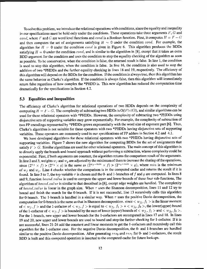
5.3 Equalities and Inequalities
The efficiency of Clarke's algorithm for relational operations of two HDDs depends on the complexity of computing H = F-G. The complexity of subtracting two HDDs is 0(IFI x IGI), and similar algorithms can be used for these relational operators with *PHDDs. However, the complexity of subtracting two *PHDDs using disjunctive sets of supporting variables may grow exponentially. For example, the complexity of subtraction of two FP encodings represented by *PHDDs grows exponentially with the word size of exponent part [6]. Thus, Clarke's algorithm is not suitable for these operators with two *PHDDs having disjunctive sets of supporting variables. These operators are commonly used in our specifications of FP adders in Section 4.2 and 4.1.
We have developed algorithms for these relational operators with two *PHDDs having disjunctive sets of supporting variables. Figure 7 shows the new algorithm for computing BDDs for the set of assignments that satisfy F > G. Similar algorithms are used for other relational operators. The main concept of this algorithm is to directly apply the branch-and-bound approach without performing a subtraction, whose complexity could be exponential. First, if both arguments are constant, the algorithm returns the comparison result of the arguments. In line 2 and 3, weights Wf and wg are adjusted by the minimum of them to increase the sharing of the operations, since (2wf x /) > (2™<> x g) is the same as (2wf-min x /) > (2w9~min x g), where min is the minimum of wj and wg. Line 4 checks whether the comparison is in the computed cache and returns the result if it is found. In line 5 to 7, the top variable r is chosen and the 0- and 1-branches of / and g are computed. In lines 8 and 9, function bound-value is used to compute the upper and lower bounds of these four sub-functions, The algorithm of bound-value is similar to that described in [8], except edge weights are handled. The complexity of bound-value is linear in the graph size. When r uses the Shannon decomposition, lines 11 and 12 try to bound and finish the search for the 0-branch. If it is not successful, line 13 recursively calls this algorithm for 0-branch. The 1-branch is handled in a similar way. When r uses the positive Davio decomposition, the computation for 0-branch is the same as that in Shannon decomposition, since < wfl, /i > is the linear moment of < wf, / > and the 1 -cofactor of < wf, f > is equal to < wfl, fi > + < wfo, f0 >, the lower(upper) bound of the 1 -cofactor of < wf, f > is bounded by the sum of lower (upper) bounds of < w^,fi > and <Wf0,fo>. For the 1-branch, new upper and lower bounds for the 1-cofactors are recomputed in lines 17 and 18. In lines 19 and 20, new upper and lower bounds are used to bound and stop the further checking for 1-cofactor. If it is not successful, lines 21-24 add the constant and linear moments to get the 1-cofactors and recursively call this algorithm for the 1-cofactor case. For the negative Davio decomposition, the 0- and 1-branches are handled similar to the positive Davio decomposition. After generating reso and res\ for 0- and 1-cofactors, the result BDD is built and this computed operation is inserted to the computed cache for future lookups.
12

bdd greater_than(< Wf,f>,<wg,g>) 1 if both < Wf, f > and < wg, g > are terminal nodes,
return ((< wfJ>)>(<wg,g >)) ? TRUE : FALSE; 2 min <- minimum(w/, w3); 3 Wf 4— Wf— min; ws <— ws— min; 4 if the operation (greater.than, < wj, / >, < wg, g >) is in computed cache,
return re«wZf found in cache; 5 T <r- top variable of / and g 6 < Wf0, /o >, < u'/,, /i >«— 0- and 1-branch of < wj, / > with respect to variable r ; 7 < wgo,g0>,< wgi,gi><- 0- and 1 -branch of < wg, g > with respect to variable T ; 8 bound_value(< Wf0, f0 >, Mpperj0,/ower/0);bound_value(< wgo,go >, uppergo, lowergo); 9 bound_value(< tu/j, /i >, upper fx, lower ft); bound_value(< wgi ,g\>, upperm, lower gi); 10 if (r uses the Shannon decomposition) { 11 if (upperf0 < lowergo) reso <— FALSE; 12 else if (/ower^0 > uppergo) reso <— TRUE; 13 else res0 <- greater_than(< w/o, /o >,< w9o, 50 >)", 14 res\ is computed similar to reso; 15 } else if (r uses the positive Davio decomposition)! 16 reso is computed the same as reso in Shannon decomposition; 17 upper ft «— uppery, + uppery0; uppergt <— upper gi + uppergo; 18 lowerf1 «— lowerf1 + lower f0; lowergi <— lowergi + lowergo; 19 if {upper fx < lowergi) res\ t- FALSE; 20 else if (lower ft > uppergi)res\ 4-TRUE; 21 else { 22 < w/,, /1 > <- addition(< wfl,fi>,< wh, f0 >);
< Wgntfi > <- addition(< iu3l,#i >, < wgo,fl0 >); 23 resj 4- greater_than(< u^, /1 >,< tuffl, 51 >); 24 } 25 } else if (r uses the negative Davio decomposition)! 26 reso and resx are computed similar to positive Davio decomposition. 27 } 28 result <— find BDD node (T, reso, res\) in unique table, or create one if not exists. 29 insert (greater.than, < Wf,f >,< wg,g >,result) into the computed cache 30 return result;
Figure 7: Improved algorithm for F > G. F =< Wf, f > and G =< wg,g >.
13

Figure 8: *PHDDs for F and G.
This algorithm works very well for two *PHDDs with disjunctive set of supporting variables, while Clarke's algorithm has exponential complexity. For example, let F = n"=0 22'XXt and G = n?=o 22' *m ■ The variable ordering is xn,yn,..., x0, y0 and all variables use the Shannon decomposition. The *PHDDs for F and G have the structure shown in Figure 8. It can be proven that the complexity of this algorithm for this type of function is O(n) if the computed cache is a complete cache.
5.4 Short-Circuiting Technique
Can we verify the specifications of FP adders by conditional forward simulation? In our experience, all specifications for the FP adder design without a mantissa comparator, as in Figure 2.a, can be verified by conditional forward simulation, but not so for the FP adder containing a mantissa comparator, as in Figure 2.b. This is caused by a conflict of variable orderings for the mantissa adder and the mantissa comparator, which generates the signal Mx < My (i.e. signal d in Figure 3). The best variable ordering for the comparator is to interleave the two vectors from the most significant bit to the least significant bit (i.e., zm-i. J/m-i. •••> ^o, yo)- Table 2 shows the CPU time in seconds and the BDD size of the signal d under different variable orderings, where ordering offset represents the number of bit offset from the best ordering. For example, the ordering is xm_1; ..., xm_6, ym-u xm_7, ym_2, ..., x0, y5, ..., yo, when the ordering offset is 5. Clearly, the BDD size grows exponentially with the offset. In contrast to the comparator, the best ordering for the mantissa adder is xm-lt ..., zm_jfe_i, ym-i, xm-k-2, Vm-2, »., so, yk, .... yo, when the exponent difference is k. We observed that the best ordering for the specification represented by *PHDDs is the same ordering as the best ordering for the mantissa adder. Thus, the extended word-level SMV can not build the BDDs for both the mantissa comparator and mantissa adder by conditional forward simulation, when the exponent difference is large.
Let us examine the compare unit carefully. We find that the signal d is used only when Ex = Ey. In other words, it is not necessary to build the BDDs for it, when \EX - Ey\ is greater than 0. Based on this fact, we introduce a short-circuiting technique to eliminate unnecessary computations as early as possible. The word-level SMV and *PHDD packages are modified to incorporate this technique. In the *PHDD package, the BDD operators, such as And and Or, are modified to abort the operation and return a special token when
14

Ordering Offset BDD Size CPU Time (Sec.) 0 157 0.68 1 309 0.88 2 608 1.35 3 1195 2.11 4 2346 3.79 5 4601 7.16 6 9016 13.05 7 17655 26.69 8 34550 61.61 9 67573 135.22 10 132084 276.23
Table 2: Performance measurements of a 52-bit comparator with different orderings.
the number of newly created BDD nodes within this BDD call is greater than a size threshold. In word-level SMV, for an And gate with two inputs, if the first input evaluates 0, 0 will be returned without building the BDDs for the second input. Otherwise, the second input will be evaluated. If the second input evaluates to 0 and the first input evaluates to a special token, 0 is returned. Similar technique is applied to Or gates with two inputs. Nand{Nor) gates can be decomposed into Not and And {Or) gates and use the same technique to terminate earlier. For other logic gates with two inputs, the result is a special token, if any of the inputs evaluates to a special token. If the special token is propagated to the output of the circuit, then the size threshold is doubled and the output is recomputed. This process is repeated until the output BDD is built. For example, when the exponent difference is 30, the size threshold is 10000, the ordering is the best ordering of mantissa adder, and the evaluation sequence of the compare unit shown in Figure 3 is d, e, f, g and h, the values of signals d, e, f, g and h will be special token, 0, 0, 1, and 1, respectively, by conditional forward simulation. With these modification, the new system can verify all of the specifications for both types of FP adders by conditional forward simulation. We believe that this short-circuiting technique can be generalized and used in the verification which only exercises part of the circuits.
6 Verification of FP Adders
In this section, we used the FP adder in the Aurora IE Chip [16], designed by Dr. Huff as part of his PhD dissertation at the University of Michigan, as an example to illustrate the verification of FP adders. This adder is based on the same approach as the SNAP FP adder [20] at Stanford University. Dr. Huff found several errors with the approach described in [20]. This FP adder only handles operands with normal values. When the result is a denormal value, it is truncated to 0. This adder supports IEEE double precision format and the 4 IEEE rounding modes. In this verification work, we verify the adder only in round to nearest mode, because we believe that the round to nearest mode is the hardest one to verify. All experiments were carried out on a Sun 248 MHz UltraSPARC-H server with 1.5 GB memory.
The FP adder is described in the Verflog language in a hierarchical manner. The circuit was synthesized into flattened, gate-level Verflog, which contains latches, multiplexors, and logic gates, by Dr. John Zhong at SGI. Then, a simple Perl script was used to translate the circuit from gate-level Verflog to SMV format.
15

6.1 Latch Removal
Huff's FP adder is a pipelined, two phase design with a latency of three clock cycles. We handled the latches during the translation from gate-level Verflog to SMV format. Figure 9.a shows the latches in the pipelined, two phase design. In the design, phase 2 clock is the complement of the phase 1 clock. Since we only verify the functional correctness of the design and the FP adder does not have any feedback loops, the latches can be replaced by And gates, as shown in Figure 9.b, without losing the functional behavior of the circuit. Since phase 2 clock is the complement of the phase 1 clock, we must replace the phase 2 clock by the phase 1 clock. Otherwise the circuit behavior will be incorrect.
Phase 1 clock
. Phase 2 clock
Phase 1 clock
. Phase 1 clock
(a) (b)
Figure 9: Latch Removal, (a) The pipelined, two phase design, (b) The design after latch removal.
6.2 Design with Bugs
In this section, we describe our experience with the verification of a FP adder with design errors. During the verification process, our system found several design errors in Huff's FP adder. These errors were not caught by random simulation performed by Dr. Huff.
The first error we found is the case when A + C = 01.111...11, A + C + 1=10.000...00, and the rounding logic decides to add 1 to the least significant bit (i.e., the result should be A + C + 1), but the circuit design outputs A+C as the result. This error is caused by the incorrect logic in the path select unit, which categorized this case as a no shift case instead of a right shift by 1. While we were verifying the specification of true addition, our system generated a counterexample for this case in around 50 seconds. To ensure that this bug is not introduced by the translation, we have used Cadence's Verilog simulation to verify this bug in the original design by simulating the input pattern generated from our system. Another design error we found is in the sticky
1. Nr
AL
L G R S
Figure 10: Sticky bit generation, when Ex - Ey = 54.
bit generation. The sticky bit generation is based on the table given in page 10 of Quach's paper describing the SNAP FP adder [20]. The table only handles cases when the absolute value of the exponent difference is
16

less than 54. The sticky bit is set 1 when the absolute value of the exponent difference is greater than 53 (for normal numbers only). The bug is that the sticky bit is not always 1 when the absolute value of the exponent difference is equal to 54. Figure 10 shows the sticky bit generation when Ex - Ey = 54. Since Nx has 52 bits, the leading 1 will be the Round (R) bit and the sticky (5) bit is the OR of all of Ny bits, which may be 0. Therefore an entry for the case \EX — Ey\ = 54 is needed in the table of Quach's paper [20].
From our experience, the design in the mantissa path doesn't cause the *PHDD explosion problem. However, when the error is in the exponent path, the *PHDD may grow exponentially while building the output. A useful tip to overcome the *PHDD explosion problem is to reduce the exponent value to a smaller range by changing the exponent range condition in Condjadd or Condsub in Equation 5, 6 or 7.
6.3 Corrected Designs
After identifying the bugs, we fixed the circuit in the SMV format. In addition, we created another FP adder by adding the compare unit in Figure 2.b into Huff's FP adder. This new adder is equivalent to the FP adder in Figure 2.b, since the ones complement unit will not be active at any time.
To verify the FP adders, we combined the specifications for both addition and subtraction instructions into the specification of true addition and subtraction. We use the same specifications to verify both FP adders. Table 3 shows the CPU time in seconds and the maximum memory required for the verification of both FP adders. The CPU time is the total time for verifying all specifications. For example, the specifications of true addition are partitioned into 18 groups and the specifications in the same group use the same variable ordering. The CPU time is the sum of these 18 verification runs. The FP adder II can not be verified by conditional forward simulation without the short-circuiting technique. The maximum memory is the maximum memory requirement of these 18 runs. For both FP adders, the verification can be done within two hours and requires less than 55 MB. Each individual specification can be verified in less than 200 seconds.
Case FP adder I FP adder II
CPU Time (Sec.) Max. Memory(MB) CPU Time (Sec.) Max. Memory(MB) True addition 3283 49 3329 55
True subtraction(/ar) 2654 35 2668 35 True subtraction (close) 994 53 1002 48
Table 3: Performance measurements of verification of FP adders. FP adder I is Huff's FP adder with bugs fixed. FP adder II is FP adder I with the compare unit in Figure 2.b. For true subtraction, far represent cases \EX - Ey\ > 1, and close represent cases \EX - Ey\ < 1.
In our experience, the decomposition type of the subtrahend's variables for the true subtraction cases is very important to the verification time. For the true subtraction cases, the best decomposition type of the subtrahend's variables is negative Davio decomposition. If the subtrahend's variables use the positive Davio decomposition, the *PHDDs for OUT can not be built after a long CPU time (> 4 hours).
As for the coverage, the verified specifications cover 99.78% of the input space for the floating-point adders in IEEE round-to-nearest mode. The uncovered input space (0.22%) is caused by the unimplemented circuits for handling the cases of any operands with denormal, NaN or oo values, and the cases where the result of the true subtraction is denormal value.
Our results should not be compared with the results in [7], since the FP adders handle difference precision (i.e., their adder handles IEEE extended double precision) and the CPU performance ratio of two different machines is unknown (they used a HP 9000 workstation with 256MB memory). Moreover, their approach
17
partitioned the circuit into sub-circuits which are verified individually based on the assumptions about their inputs, while our approach is implementation-independent.
7 Conversion Circuits
The overflow flag erratum of the FIST instruction (floating-point to integer conversion) [14] in Intel's Pentium Pro and Pentium II processors has illustrated the importance of verification of the conversion circuits [ 16] which convert the data from one format to another format (e.g., IEEE single precision to double precision). These circuits are another common unit in floating-point processors. For example, the MIPS processor supports conversions between any of the three number formats: integer, IEEE single precision, and IEEE double precision.
We believe that the verification of the conversion circuits is much easier than the verification of floating-point adders, since these circuits are much simple than the floating-point adders and only have one operand(i.e. less variables than FP adders). For example, the specification of the double-to-single (D2S) operation, which con- verts the data from double precision to single precision, can be written as "(overflow.flag = expected-overflow) & (not overflow-flag =$■ (output = expected-output))", where overflow .flag and output are directly from the circuit as well as expected-overflow and expected-.output are computed in terms of the inputs, since some of the numbers represented in double precision cannot be represented in single precision. For example, ex- pected-output is computed by Round((-\)s x M X 2E~B). Similarly, expected-overflow can be computed from the inputs.
For another example, the specification of the single-to-double (S2D) operation, which converts the data from single precision to double precision, can be written as "output = input", since every number represented in single precision can be represented in double precision without rounding(i.e. the output represents the exact value of input).
8 Conclusions and Future Work
We presented extensions to word-level SMV to enable the verification of floating-point adders with implementation- independent specifications. Word-level SMV were improved by using the Multiplicative Power HDD (*PHDD) representation, by deriving efficient algorithms for equality and inequality operations between two *PHDDs, and by incorporating conditional symbolic simulation as well as a short-circuiting technique. Based on the case analysis of the signs and the relations of two exponents, the specifications of floating-point adders are divided into several hundreds of implementation-independent sub-specifications.
Conditional forward simulation has the advantage of implementation-independent specifications. We iden- tified a conflict in the variable orderings between the mantissa comparator and mantissa adder which prevents the use of conditional forward simulation. We presented a short-circuiting technique to solve this problem. This short-circuiting technique can be generalized and used in the verification which only exercises part of the circuits.
We used our system and the implementation-independent specifications to verify a FP adder from University of Michigan. Our system found several bugs in Huff's FP adder and generated counterexamples within several minutes. After fixing the bugs, a variant of the Aurora HI FP adder is created by introducing a mantissa comparator and extra circuits for demonstrating the capability of our system to handle different FP adder designs. For each of FP adders, the verification task finished in 2 CPU hours on a Sun UltraSPARC-E server for IEEE double precision. The verified specifications covered 99.78% of the entire input space. The uncovered input space (0.22%) We believe that our system and specifications can be applied to directly verify FP adders
18

and to help finding design errors. The overflow flag erratum of the FIST instruction (floating-point to integer conversion) [14] in Intel's Pentium
Pro and Pentium II processors has illustrated the importance of verification of the conversion circuits which convert the data from one format to another format (e.g., IEEE single precision to double precision). Since these circuits are much simpler than floating-point adders and only have one input operand, we believe that our system can be used to verify the correctness of these circuits. We plan to verify the conversion circuits in the Aurora HI chip.
Acknowledgement
We thank Prof. Brown, Dr. Huff and Mr. Riepe at University of Michigan for providing us with Huff's FP adder and valuable discussions. We thank Dr. John Zhong at SGI for helping us to synthesize the Huff's FP adder design into flattened, gate-level Verflog. We thank Henry A. Rowley for providing us the simple Perl script.
References
[1] AAGAARD, M. D., AND SEGER, C.-J. H. The formal verification of a pipelined double-precision IEEE floating-point multiplier. In Proceedings of the International Conference on Computer-Aided Design (November 1995), pp. 7-10.
[2] BRYANT, R. E. Graph-based algorithms for boolean function manipulation. In IEEE Transactions on Computers (August 1986), pp. 8:677-691.
[3] BRYANT, R. E., BEATTY, D. L., AND SEGER, C.-J. H. Formal hardware verification by symbolic ternary trajectory. In Proceedings of the 28th ACM/IEEE Design Automation Conference (June 1991), pp. 397- 402.
[4] BRYANT, R. E., AND CHEN, Y.-A. Verification of arithmetic circuits with binary moment diagrams. In Proceedings of the 32nd ACM/IEEE Design Automation Conference (June 1995), pp. 535-541.
[5] CARREräO, V. A., AND MINER, P. S. Specification of the IEEE-854 floating-point standard in HOL and PVS. In High Order Logic Theorem Proving and Its Applications (September 1995).
[6] CHEN, Y.-A., AND BRYANT, R. E. *PHDD: An efficient graph representation for floating point circuit verification. In Proceedings of the International Conference on Computer-Aided Design (November 1997), pp. 2-7.
[7] CHEN, Y.-A., CLARKE, E. M., HO, P.-H., HOSKOTE, Y, KAM, T, KHAIRA, M., O'LEARY, J., AND ZHAO,
X. Verification of all circuits in a floating-point unit using word-level model checking. In Proceedings of the Formal Methods on Computer-Aided Design (November 1996), pp. 19-33.
[8] CLARKE, E. M., FUJITA, M., AND ZHAO, X. Hybrid decision diagrams - overcoming the limitations of MTBDDs and BMDs. In Proceedings of the International Conference on Computer-Aided Design (November 1995), pp. 159-163.
[9] CLARKE, E. M., KHAIRA, M., AND ZHAO, X. Word level model checking - Avoiding the Pentium FDrV error. In Proceedings of the 33rd ACM/IEEE Design Automation Conference (June 1996), pp. 645-648.
19
[10] CLARKE, E. M., MCMILLAN, K., ZHAO, X., FUJITA, M., AND YANG, J. Spectral transforms for large Boolean functions with applications to technology mapping. In Proceedings of the 30th ACM/IEEE
Design Automation Conference (June 1993), pp. 54-60.
[11] COE, T. Inside the Pentium Fdiv bug. Dr. Dobbs Journal (April 1996), pp. 129-135.
[12] COUDERT, O., AND MADRE, J. C. A unified framework for the formal verification of sequential circuits. In Proceedings of the International Conference on Computer-Aided Design (November 1990), pp. 126-129.
[13] DRECHSLER, R., BECKER, B., AND RUPPERTZ, S. K*BMDS: a new data struction for verification. In
Proceedings of European Design and Test Conference (March 1996), pp. 2-8.
[14] FISHER, L. M. Flaw reported in new intel chip. New York Times (May 6 1997), D, 4:3.
[15] HAMAGUCm, K., MORTTA, A., AND YAJIMA, S. Efficient construction of binary moment diagrams for verifying arithmetic circuits. In Proceedings of the International Conference on Computer-Aided Design
(November 1995), pp. 78-82.
[16] HUFF, T. R. Architectural and circuit issues for a high clock rate floating-point processor. PhD Dissertation
in Electrical Engineering Department, University of Michigan (1995).
[17] JAIN, P., AND GOPALAKRISHNAN, G. Efficient symbolic simulation-based verification using the parametric form of boolean expressions. In IEEE Transactions on Computer-Aided Design of Integrated Circuits and
Systems (August 1994), pp. 1005-1015.
[18] LEESER, M., AND O'LEARY, J. Verification of a subtractive radix-2 square root algorithm and implemen- tation. In Proceedings of 1995 IEEE Internaational Conference on Computer Design: VLSI in Computer
and Processors (October 1995), pp. 526-531.
[19] MCMILLAN, K. L. Symbolic Model Checking. Kluwer Academic Publishers, 1993.
[20] QUACH, N., AND FLYNN, M. Design and implementation of the SNAP floating-point adder. Tech. Rep. CSL-TR-91-501, Stanford University, December 1991.
[21] RUEß, H., SHANKAR, N., AND SRIVAS, M. K. Modular verification of SRT division. In Computer-Aided Verification, CAV '96 (New Brunswick, NJ, July/August 1996), R. Alur and T. A. Henzinger, Eds., no. 1102 in Lecture Notes in Computer Science, Springer-Verlag, pp. 123-134.
[22] SHARANGPANI, H. P., AND BARTON, M. L. Statistical analysis of floating point flag in the pentium processor(1994). Tech. rep., Intel Corporation, November 1994.
[23] SUZUKI, H, MORINAKA, H, HIROSHI MAKINO, NAKASE, Y., MASHIKO, K., AND Suva, T. Leading-zero anticipatory logic for high-speed floating point addition. IEEE Journal of Solid-State Circuits (August
1996), pp. 1157-1164.
[24] ZHAO, X. Verification of arithmetic circuits. Tech. Rep. CMU-CS-96-149, School of Computer Science,
Carnegie Mellon University, 1996.
20