Verification of Complex Analog Integrated Circuits€¦ · · 2015-07-28Verification of Complex...
20
Copyright © 2006, Designer’s Guide Consulting, Inc. – All Rights Reserved 1 of 20 Version 1a, 1 March 2005 Functional complexity in analog, mixed-signal, and RF (A/RF) designs is increasing dramatically. Today’s simple A/RF functional block such as an RF receiver or power management unit can have hundreds to thousands of control bits. A/RF designs implement many modes of operation for different stan- dards, power saving modes, and calibration. Increasingly, catastrophic failures in chips are due to functional bugs, and not due to missed performance specifi- cations. Functionally verifying A/RF designs is a daunting task requiring a rig- orous and systematic verification methodology. As occurred in digital design, analog verification is becoming a critical task that is distinct from design. This paper describes a verification methodology to address these challenges. The is paper was presented at the 2006 Custom Integrated Circuits Conference in September 2006. It was last updated on September 26, 2006. You can find the most recent version at www.designers-guide.com. Contact the authors via e-mail at [email protected]. Permission to make copies, either paper or electronic, of this work for personal or classroom use is granted without fee provided that the copies are not made or distributed for profit or commercial advantage and that the copies are complete and unmodified. To distribute other- wise, to publish, to post on servers, or to distribute to lists, requires prior written permission. Designer’s Guide is a registered trademark of Kenneth S. Kundert. All rights reserved. Verification of Complex Analog Integrated Circuits Ken Kundert Henry Chang
Transcript of Verification of Complex Analog Integrated Circuits€¦ · · 2015-07-28Verification of Complex...

Verification of Complex Analog Integrated Circuits
Ken KundertHenry Chang
Version 1a, 1 March 2005 Functional complexity in analog, mixed-signal, and RF (A/RF) designs is increasing dramatically. Today’s simple A/RF functional block such as an RF receiver or power management unit can have hundreds to thousands of control bits. A/RF designs implement many modes of operation for different stan-dards, power saving modes, and calibration. Increasingly, catastrophic failures in chips are due to functional bugs, and not due to missed performance specifi-cations. Functionally verifying A/RF designs is a daunting task requiring a rig-orous and systematic verification methodology. As occurred in digital design, analog verification is becoming a critical task that is distinct from design. This paper describes a verification methodology to address these challenges.
The is paper was presented at the 2006 Custom Integrated Circuits Conference in September2006. It was last updated on September 26, 2006. You can find the most recent version atwww.designers-guide.com. Contact the authors via e-mail at [email protected].
Permission to make copies, either paper or electronic, of this work for personal or classroomuse is granted without fee provided that the copies are not made or distributed for profit orcommercial advantage and that the copies are complete and unmodified. To distribute other-wise, to publish, to post on servers, or to distribute to lists, requires prior written permission.
Designer’s Guide is a registered trademark of Kenneth S. Kundert. All rights reserved.
Copyright © 2006, Designer’s Guide Consulting, Inc. – All Rights Reserved 1 of 20

Verification of Complex Analog Integrated Circuits Introduction
1 Introduction
During the past decade, analog, mixed-signal, and radio frequency (A/RF) design has undergone dramatic changes primarily driven by thecompetitive pressures of the consumer marketplace. In these consumersystems, A/RF plays a critical role providing the interface to the con-sumer and enabling high-bandwidth communication channels withinthe system and between systems. The challenges facing the A/RFdesigner are daunting. These include achieving the desired functionalitywith the required performance, providing this at the lowest cost andpower possible, and finishing before the competition. A fundamentalchange is occurring that is driving failure in A/RF designs. There is anexplosion in functional complexity that results in existing ad hoc verifi-cation methodologies becoming overwhelmed.
Complexity is exploding in A/RF design in multiple dimensions simul-taneously. The primary culprit for the complexity explosion is that thenumber of modes of operation of today’s A/RF designs is increasing dueto several factors. First, there is a need to support a large number newand legacy worldwide standards and each standard then has their ownunique modes of operation. To increase battery life, all of today’s ICshave various power saving modes. And A/RF designs themselves havedifferent circuit operating modes to perform their basic functions. A sim-ple analog block such as an Analog-to-Digital Converter (ADC) or aPhase-Locked Loop (PLL) can have 10 to 30 digital control pins while ananalog functional unit such as a power management unit, RF transceiv-ers, or coder/decoder (CO/DEC) could have hundreds of control pins.
Increasing performance requirements on the latest processes where thecomponents themselves are dropping in quality is forcing designers toincrease the size and behavioral complexity of their circuits to overcomethe limitations of the components. For example, they may incorporateself-calibration or error cancellation schemes; or they may choose to usealgorithmic sampled-data circuits rather than simpler continuous-timecircuits because they are a better match to the features of advancedCMOS processes [1,2,6,8,9]. Finally, advanced processes make manymore transistors available that are used to add new features or increasethe level of integration.
Each of these things individually (number of operating modes, behav-ioral complexity, and circuit size) contribute to making the process ofverifying a design substantially more difficult, but all three are at worksimultaneously and combine to overwhelm all existing approaches atverification. Functional failures in A/RF are now taking precedent overfailures stemming from not meeting performance specifications. Func-tional failures can come in the form of inoperable modes and are oftendue to “simple” errors such as inverted signals, swapped bit lines, and
2 of 20 Designer’s Guide Consultingwww.designers-guide.com

Existing Approaches Verification of Complex Analog Integrated Circuits
incorrect power up sequencing. Functional failures tend to result infailed chips that are show stoppers as the end customer cannot beginbringing up the firmware that is typically run on the SoCs. In contrast, aperformance failure is not as fatal because the system development canusually continue while the IC is re-spun for performance improvement.The end result of functional failures is many design iterations (re-spins).These are usually at great expense in terms of non-recurring engineeringcosts (NRE) and missed market windows.
As happened in digital design in the late 1990’s, complexity is now over-whelming design teams and causing errors in the design of A/RF ICs,functional units, and basic building blocks. The question on the minds ofdesign managers is no longer whether there is a error in the design ornot, but rather how many there are and how many spins it will take tofind them. In digital design, verification separated from design andtoday dominates the majority of the engineering effort. A similar processmust now occur for analog designs.
This paper describes a systematic A/RF functional verification method-ology and provides a starting point for the A/RF design team and verifi-cation engineer.
2 Existing Approaches
Many approaches and combinations of approaches are used today toaddress the complexity and teamwork challenges.
2.1 Design Approaches
Understanding that verification is a daunting challenge with no easysolution, designers try to reduce the need for verification. There are sev-eral approaches:• Separate analog and digital — the need for verification in the A/RF
team is reduced because the digital functionality has been moved out. • Everything programmable — make all functions controllable, so that
if there are errors in the design these errors can be corrected in firm-ware.
• Everything tunable — make all resistors, capacitors, current sources,and voltages sources tunable to boost performance and to tune outprocess imperfections.
Although these are powerful techniques, substantial penalties are paidfor employing these approaches. And in many cases, although conceptu-ally the design is simpler, the number of control bits actually increase,thus leaving open the possibility for more design bugs.
3 of 20Designer’s Guide Consultingwww.designers-guide.com
Verification of Complex Analog Integrated Circuits Verification Methodology
Also, knowing the limitations of the design tools, simulators, and otherconstraints, designers often limit their design choices to avoid potentialproblems. In particular, without a strong verification methodology,promising yet complex architectures may be avoided.
2.2 CAD Approaches
Almost all approaches center on the idea of accelerating simulation.They include mixed-mode simulation (mixing transistor and register-transfer level (RTL) descriptions); mixed-level simulation (mixing func-tional models and transistors); and using fast simulators that exploit thecharacteristics of the circuit, such as timing simulators and RF simula-tors. These approaches all require additional effort and engineeringtrade-off decisions on the part of the A/RF designer — usually accuracyvs. speed. Although these approaches can increase simulation speed,without a systematic verification process to provide context for the sim-ulation, it is difficult to correlate additional simulation speed to howmany bugs remain in the design.
3 Verification Methodology
The goal of the verification methodology is to systematically find errorsin A/RF designs in a reproducible manner. It also provides several sub-stantial collateral benefits. It tends to make the design process itself moreefficient and predictable [4,5]. It produces verified models and test-benches of the design that aid in reuse, integration, and test programdevelopment. It can be used to accelerate performance verification. Andit tends to uncover errors in the specification documentation.
3.1 Key Concepts
3.1.1 Verification Plan
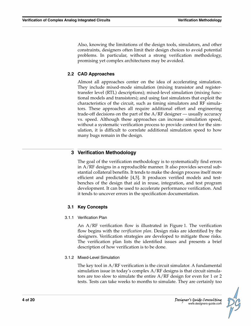
An A/RF verification flow is illustrated in Figure 1. The verificationflow begins with the verification plan. Design risks are identified by thedesigners. Verification strategies are developed to mitigate those risks.The verification plan lists the identified issues and presents a briefdescription of how verification is to be done.
3.1.2 Mixed-Level Simulation
The key tool in A/RF verification is the circuit simulator. A fundamentalsimulation issue in today’s complex A/RF designs is that circuit simula-tors are too slow to simulate the entire A/RF design for even for 1 or 2tests. Tests can take weeks to months to simulate. They are certainly too
4 of 20 Designer’s Guide Consultingwww.designers-guide.com
Verification Methodology Verification of Complex Analog Integrated Circuits
slow for the hundreds to thousands of tests needed to cover all the oper-ating modes. At the heart of this methodology is a technique calledmixed-level simulation [4,5] to work around this issue. Mixed-level simu-lation is a means by which HDL or AHDL models can be run with tran-sistor level models. For example, in a particular test, the critical circuitsbeing tested will be left at transistor level while the non-critical circuitssuch as bias currents or digital logic will be left at AHDL or HDL respec-tively. In this way, simulations can run hundreds to thousands of timesfaster. In this paper, we use Verilog-AMS [4] for our AHDL and Verilogfor our HDL.
3.1.3 Modeling and Simulation Plans
Because mixed-level simulation is not as straightforward as simulatingthe entire design at the transistor level, careful planning is required toensure verification is done properly. The modeling plan and the simulationplan are the processes by which the verification plan is implemented.Typically, there is a top-level model and the block models. The top-levelmodel serves as the “sign-off” quality executable specification delivered tothe integrator of the functional unit. The modeling plan describes whatAHDL and HDL models need to be written, and the simulation plandescribes all of the simulation configurations that need to be run. Config-urations specify for each test which part of the circuit should be at tran-sistor level. The block models are used to enable mixed-level simulation.
3.1.4 Self-Checking Testbench
Full benefit from this methodology is derived with applying a self check-ing testbench. The self checking testbench drives the circuit and captures
FIGURE 1 The A/RF verification flow.
Verification Plan
Modeling Plan Simulation Plan
Design
Design/LayoutTop-level Model
Mixed-LevelSimulations
Design Risks
Self Checking
Documentation
Block Models
Testbench
Verification EngineeringTasks
Design Tasks
Regression TestsExecutable Specification Final Design
(integration model)(pass / fail)
Start
5 of 20Designer’s Guide Consultingwww.designers-guide.com

Verification of Complex Analog Integrated Circuits Verification Methodology
the simulated results and compares them to the expected results as spec-ified in the design documentation. The expected results can be placedinline with the tests, in separate files, or a golden model can be establishedwhere the golden model itself represents the expected behavior. Thesetests are extensive, testing top-level as well as block level behavior.Mixed-level simulations are run as described in the simulation plan. Thegoal is to verify that the design matches the design intent and that thedesign matches the top-level model. The testbench is described in detailin Section 3.3. Because the documentation, design, and top-level modelare now linked, the model is, in fact, an executable specification that can bedelivered to the design’s customer and to other designers. It is a far lessambiguous means of communication than written documentation,which is often inaccurate and out of date.
The key reason for choosing the self checking approach is to enable auto-mated regression testing. Tests run automatically on a nightly or on an ‘asneeded’ basis. Summaries are posted or sent to designers to alert them toissues. It is impractical to expect designers to inspect detailed resultssuch as individual waveforms after hundreds of tests are run. Withoutautomation, the level of testing required in today’s A/RF designs is notpractical.
3.1.5 Verification Engineers
In Figure 1, note that the design and verification tasks are separated. Toexecute the verification tasks, a new engineer is required, the analog veri-fication engineer. This engineer is analogous to the digital verificationengineer. The job of this engineer(s) is to focus on verification of the A/RF design at the functional unit and the block level. There are severalreasons for requiring a new engineer.• New skills are required that are usually not present in design teams
— verification engineers must be proficient at modeling, developingtests, well versed in digital and analog modeling languages, simula-tors used in digital, mixed-mode, and analog, and scripting and batchmode operation of regression testing.
• The need to focus — developing models and tests is a substantialeffort, and in most projects is too large of a job to be done part time bya design engineer. Furthermore, designers are often consumed bytheir design and so cannot give the required attention to the verifica-tion task.
• Degree of independence — if the engineer that is designing a circuit isalso responsible for verifying it, then any misunderstanding of therequirements will pollute both the design and the tests and so will notbe caught. This is much less likely to happen with a verification engi-neer, especially if the verification engineer keeps a certain distancefrom the design engineers and works primary from the specification.
6 of 20 Designer’s Guide Consultingwww.designers-guide.com
Verification Methodology Verification of Complex Analog Integrated Circuits
The analog verification engineer does not have to be as design knowl-edgeable as the analog designer as they will not be designing, but theydo need to understand analog design concepts and techniques, terminol-ogy, and the use of analog design tools.
Key to this methodology is separating roles and responsibilities. Theverification engineer should never modify the design. The designer cansuggest additions to the testbench, but it is the verification engineer whomust approve changes. Furthermore the design engineers should updatethe specifications when needed, but it is the verification engineer thatmust assure that the design conforms to the specifications.
Although this is an extra resource, the benefits can offset this burden. Itis a means to train new analog designers. Also, designers can spend lesstime on functional verification. Instead they can focus on performancevalidation and on innovating new and more promising architectures.Finally, the overall efficiency of the design can be improved as new skillsare being brought to the design team, skills that designers often lack.
3.1.6 Benefits
The key benefits of this methodology are:• Designers are always simulating their blocks in the context of the
overall functional unit• Extensive regression tests are always being run to make sure that
interfaces are correct• The design documentation, the HDL model and the design are
always synchronized.• Design time can be accelerated since errors are caught earlier.
3.2 Verification in Context of Design
The ideal design and verification project time line is shown in Figure 2.The design project begins with the creation of the specifications for theA/RF functional unit. These are generally derived by the chip systemengineer. Once the chip architecture is solidified, the system engineerworks with the A/RF design lead to formulate specifications for the ana-log portion of the design based on an estimate of what is possible in theA/RF functional unit. Reuse of existing components is often taken intoaccount.
At the functional unit level, analog architectural questions are exploredsuch as determining the best architecture for blocks and what are thedetailed parametric design values to be used. System exploration toolssuch as Matlab, Simulink, Ptolomy, and even a generic spreadsheet arehelpful in this phase because they allow designers to quickly exploretheir design and to transform the design requirements into design
7 of 20Designer’s Guide Consultingwww.designers-guide.com

Verification of Complex Analog Integrated Circuits Verification Methodology
parameters. At this point in the design flow the focus is on modeling thesignal flow through the system with an emphasis on estimatingexpected performance, so second-order effects are often included. How-ever, details such as modeling the control flow or interface detailsbetween the blocks are rarely modeled, because it would slow downarchitectural exploration.
This is the time when the analog verification lead joins the project. He/sheworks with the design lead to develop models for each block in Verilog-AMS. Verilog-AMS is used rather than a language like Matlab becausethese models will eventually be used to perform mixed-level simulation.Here the modeling focus changes from the system design phase to theimplementation phase where verification is a key focus. Only the func-tion of the blocks is modeled with little to no effort expended to model-ing second-order effects. Instead the emphasis is on modeling all of thefunctionality, including control flow and the interfaces. Thus, systemexploration tools are the tool of the design engineer, while AHDLs arefor the verification engineer. At this point, the verification engineer canalso influence the design to make it more verifiable and testable. Theoutcome of this phase is a first cut at a partitioned pin-accurate top-levelfunctional unit schematic with behavioral models for each of the blocksthat is simulatable and implements all functional aspects of the specifi-cation. The block designers now join the project.
The block designers start with the documentation, the top-level sche-matic, and the models, and use them to gain an understanding of whatthey are expected to design. Meanwhile, the verification engineer orengineers (more would join the project at this point if the design is largeor complex) would begin developing block-level and then functionalunit-level tests. This is where rigor is brought into design management.Two types of tests are developed. Quick tests are a set of basic tests thatcan ideally run in minutes and can be used by designers before they“check-in” their blocks to assure that they meet minimum functionalityand compatibility requirements. Regression tests are more extensive,
FIGURE 2 Ideal A/RF design and verification project time line.
No Benefit
Functional UnitA/RF Design Lead
A/RF Block Designers
A/RF VerificationEngineer(s)
Refinement Design Integration Layout ECO and top-levelperformance verification
Deliverables
Modeling
Functional unittestbench
Deliver early HDLmodel to customer
Block Design(includes performance verification) Layout ECO and top-level
performance verificationTransition to next project
(available for fixes)
Transition to next project(available for fixes)
Ship designto chip level
RefinementRegression Testing
RefinementRegression Testing
(w/parasitics if necessary)
Release toManufacturing
Verificationcan continue
Blocktestbenches
RefinementRegression Testing
Refinement / Regression Testing (w/parasitics if necessary)
Block verification engineers
(available for fixes)can transition to next project
Benefiting from verification Benefiting from Verification
Architecture
8 of 20 Designer’s Guide Consultingwww.designers-guide.com

Verification Methodology Verification of Complex Analog Integrated Circuits
designed for overnight runs. It is important for designers to check intheir designs often so that the verification engineer can run these moreextensive tests. It also helps to keep the overall design synchronized.With the designers’ focus on performance, they will likely also use themodels written by the verification engineer to speed up simulation byreplacing noncritical circuitry with simple functional models.
Besides developing and running tests, the verification engineers alsodevelops and tests the functional unit Verilog model if one needs to bedelivered to the customer. They would also be expected to perform veri-fication reviews that include themselves, the block designers, the analoglead, and CAD support to assure that their tests are both comprehensiveand efficient.
Once the top-level schematic and models have settled out it is possible tobring the test engineers onto the project. They would use the models tobegin developing the tests that will be used on the production floor.Bringing the test engineers in early allows the tests to be developed inparallel with the design effort. This can shorten the time to first customershipment and allows them to contribute suggestions that would makethe design more testable.
As the design approaches completion, the focus of the verification engi-neer shifts to more comprehensive functional unit-level tests. Everyblock should be simulated at the transistor level within the larger systemin a mixed-level simulation. If there is a possibility of subtle interactionbetween multiple blocks, the blocks should be simulated together at thetransistor level. An example of when this is necessary is when the designincludes a separate bias block. That block should be run pair-wise at thetransistor level with every block it feeds.
Maximum benefit is derived from this methodology if the verificationengineer is brought into the project early as shown in Figure 2.
3.3 The Testbench
Apart from the device-under-test (DUT), the testbench (shown in Figure 3)contains all of the necessary components for verification. It is the respon-sibility of the lead verification engineer to assemble the testbench.
The DUT is tested by attaching it to a testbench. The testbench providesthe inputs necessary to drive the device while monitoring its output. Theterm DUT refers to each of the multiple representations of the design —Verilog, Verilog-AMS, and Verilog-AMS mixed with transistors. Theactual testing of the DUT is performed primarily using assertions andtests [7].
9 of 20Designer’s Guide Consultingwww.designers-guide.com

Verification of Complex Analog Integrated Circuits Verification Methodology
3.3.1 Assertions
Assertions have the property that they are always checked, regardless ofwhat tests are running. An assertion is modeling code that continuallyobserves one or more signals and raises a fault when it detects an errorcondition. They can be used advantageously in several places. First, theyare in the testbench where they look for unexpected behavior from theDUT. Second, they can be placed in the models or in the circuit wherethey check that the design is being used correctly. For example, an asser-tion may monitor a bias line and an enable line to verify that the currentthrough the bias line should be 10μA ±10% if its enable line is high andzero otherwise. Other uses include checking setup and hold times,checking that illegal codes are not generated, and even checking that theinput/output characteristics of blocks are implemented properly. Asser-tions can be placed in the model or circuits that are to be delivered to anend customer. to ensure that the circuit is properly interfaced to theremainder of the system and is being used properly.
3.3.2 Tests
A test is a grouping of a stimulus, a monitor, and a comparison to checkagainst the expected response. The test applies the stimulus to the DUTand compares the achieved results with the expected results to determinea pass/fail response. The stimulus is the signal or a sequence of signalsapplied to the DUT. A monitor is used to observe the output. The moni-tor could be as simple as observing a current or voltage, or could bemore complicated, taking several signals and processing them. Addi-tional code is then added to compare against the expected results. Here,a tolerance or bounds may be needed when comparing analog signals. Afailure occurs if the comparison finds that the actual and expected resultsare different or different beyond a certain tolerance.
FIGURE 3 Elements of the self-checking testbench.
Collar
DUTStimulus
MonitorsFailures
ExpectedResults
Faults
Tests
InitializationTest 1Test 2...Test nFinish Assertions
Additional Circuitry
AHDL ModelMixed AHDL/Transistors
HDL Model
10 of 20 Designer’s Guide Consultingwww.designers-guide.com

Verification Methodology Verification of Complex Analog Integrated Circuits
3.3.3 Transactors
To enable re-use of tests within the same design or between designs,tests can be written in an abstract manner by employing a transaction-based interface to the DUT. A transaction is a sequence of signal transi-tions on a group of one or more pins that accomplishes a single task. Atransactor [7] is a block of code that acts as an interface between the testcode and the DUT by converting between high-level test instructionsand low-level transactions with the DUT.
For example, a bit-error rate (BER) test that sends a random sequence ofsymbols to a transmitter and receives the sequence that has been pro-cessed by the DUT and looks for errors could be adapted to any numberof different types of systems with the right transactors. For example,transactors that convert to and from an 8b/10b code could be used toapply the test to a SerDes. Other transactors could be used to apply thetest to a wireless transceiver, data converters, or a wide variety of signaltransmission systems. Similarly, these same transactors can be use asinterfaces for different tests. For example, to stress the DUT the BER test,which tends to produce evenly distributed random symbols, can bereplaced with a test that produces corner case symbol streams, such asthose with long run lengths. This shows that the transactors are alsoreusable if the interface between the transactors and the tests aredesigned with an eye towards reusability.
3.3.4 Collars
A collar surrounds the DUT as shown in Figure 4. The purpose of the col-lar is to create a wrapper so that the testbench can be applied withoutchange to all DUT representations. In this way, there is only one test-bench and DUT. The collar is considerably simpler than the testbenchand changes much less frequently. As such, it is much less likely that anerror would be created and go undetected if there are multiple versionsof the collar than if there are multiple versions of the testbench.
The collar performs several important functions. The first is to allow thetestbench to observe internal signals of the DUT in a manner that is por-table across all versions of the DUT. In A/RF design, there are many
FIGURE 4 The testbench connects to the DUT through a collar, which is responsible for mapping signals internal to the DUT.
DUT
Testbench
Collar
11 of 20Designer’s Guide Consultingwww.designers-guide.com
Verification of Complex Analog Integrated Circuits Verification Methodology
modes associated with small internal adjustments used for compensat-ing for second order effects. For example, a typical adjustment is for thecommon-mode voltage at the output of one stage going into another. Ifthis is not observable from the DUT’s terminals, it is desirable to probeinto the DUT and observe the common-mode voltages directly. Thislevel of the hierarchy likely does not exist in the high-level Verilogmodel. In this case we add a collar that acts as a wrapper and takesresponsibility for mapping all of the signals of interest in the DUT to itsperiphery for access by the testbench.
Another important function of the collar is to make any language con-versions required. If the testbench is in Verilog-AMS, then the collarmust covert other representations of the DUT to be Verilog-AMS com-patible. For example, Verilog does not allow for real number terminals.For the DUT models to behave properly, Verilog models have to haveanalog inputs and outputs. Fortunately, Verilog does support real vari-ables. In this case, the function of the collar is to allow external blocks toread and write values into variables associated with these inputs andoutputs.
3.3.5 Drivers and Loads
Finally, in the testbench, there may be additional circuitry such as theDUT’s load, drivers for the input, or filters at the input and output.
The testbench represents a powerful first step toward design for re-usein analog. Unlike the transistor level design which will certainly change,the testbenches can be re-used or used as a starting point with littlechange especially in the cases of a standards based design or a designshrink for cost reduction.
3.4 Writing Models, Testbenches, Regression Tests
One of the seemingly most daunting tasks is writing the models. This isnot nearly as challenging and unbounded as generally perceived if themodels are written in the context of a verification methodology.
When developing the models, the primary concern should be on model-ing the basic functionality of the block. Each model should accuratelymodel the interface of the block so that the model can replace the blockin simulation. This means the number and type of pins must match, andthe signal levels and impedances must be compatible with the rest of thecircuit. Out of bounds conditions need not be modeled, but rathershould simply put the model in a fault state so the problem can be easilyfound. Modeling second order effects should be avoided as the addi-tional code required slows both the development and execution of themodel and are orthogonal to the primary goal of verifying the function-
12 of 20 Designer’s Guide Consultingwww.designers-guide.com

Example Verification of Complex Analog Integrated Circuits
ality of the circuit. Use the verification and modeling plan as a guide todetermine the level of detail required.
An example of a typical model used during functional verification isshown in Listing 1. Notice that this model is pin-accurate in thatincludes both the supply and bias pins; the supply currents are modeled;the bias line is modeled to the degree that the circuit that supplies thebias current to the block will operate properly; the bias current and sup-ply voltage are checked to assure that they are within tolerance; and thatthe function of the block is modeled at a very simple idealized level.
4 Example
To illustrate the verification methodology, we provide a relatively simpleexample of an A/RF functional unit. The block diagram is shown inFigure 5. The inputs/outputs (I/O) of the functional unit are shown onthe left and right. The control lines for each of the blocks are shown atthe top and the bottom. All of the block control lines, a total of 108, gothrough the control register on the left so that all blocks can be controlledexternally. This example illustrates the style of design where all controlpins are exported. The number of control bits could be reduced by add-ing more control logic internally, but the same number of modes wouldstill need to be tested and any errors in this logic could not be correctedin software.
LISTING 1 Verilog-AMS functional model of a flash ADC.
module flash( out, in, clk, bias, pwrdn, vdd );input in, clk, bias, pwrdn, vdd;output [15:0] out;electrical in, bias, vdd;integer i, level;reg pwrFault, biasFault;reg [15:0] d;
always @(posedge clk) beginpwrFault = (V(vdd) > 1.9) || (V(vdd) < 1.7);biasFault = (I(vdd,bias) > 16u) || (I(vdd,bias) < 14u);level = 16∗(V(in)+0.5); // convert input to an integerfor (i=0; i<16; i=i+1)
d[i] = (i < level);endassign out = (pwrdn || pwrFault || biasFault) ? 16’bx : d;
analog beginV(vdd,bias) <+ pwrdn ? 0 : 0.5 + 20k∗I(vdd,bias);I(vdd) <+ pwrdn ? 1u : 500u;
endendmodule
13 of 20Designer’s Guide Consultingwww.designers-guide.com

Verification of Complex Analog Integrated Circuits Example
This design has 113 control pins, 40 signal inputs and 4 signal outputs.Therefore, there are 2113 possible control combinations with 240 inputcombinations. Of course, most of the modes are independent and not allcombinations have to be validated. This is why the verification plan iscritical.
Finally, there are 4 design engineers on this design — a design lead, ablock designer for the DACs, a designer for the amplifiers, and adesigner for all the digital circuitry.
This example focuses on functional unit level verification where theblocks are verified in the context of the functional unit. This best demon-strates the power of the methodology.
4.1 The Verification Flow
The verification flow begins with the verification plan. The verificationengineer works with the lead designer to determine what is most criti-cal. The following is determined to be critical:• Nominal operation — all control bits are set at default values and the
DACs must run through all codes.• Mode Tests — each of the control bits must be exercised from the top-
level and compared against expected results• Special Modes — certain combinations of modes are critical and must
be tested from the top-level and compared against expected results• Test mode — the functional unit must be able to be controlled via the
scan control lines
Next, the modeling plan is developed. The following are the models thatneed to be built.
FIGURE 5 Example A/RF functional unit.
DAC 4
Power
Mode[1:0]
R tune[3:0]
C tune[3:0]
Com
mon
Mode[3:0]
Power
Mode[1:0]
Gain[3:0]
DAC 3
DAC 2
DAC 1
Reference Generator
DA
C B
ias1[3:0]
DA
C B
ias2[3:0]
Am
p Bias
[3:0]
Power
Mode[1:0]
a1
a2
a3
a4
ExternalVddInternal Vdd
ClockDivider
Clk Select
[3:0]
External Clk
InputSelect
10bcounter
controlregister
Sequence[1:0]
Reset
InputSelect[5:0]
Scan inScan out
Test modeScan Control
Test clock
Clk
DAC1[9:0]DAC2[9:0]DAC3[9:0]DAC4[9:0]
Scan Input[39:0]All block control signals
108
SupplySelect
14 of 20 Designer’s Guide Consultingwww.designers-guide.com
Example Verification of Complex Analog Integrated Circuits
• Functional unit HDL model — this is to be delivered to the integra-tors of this design.
• Functional unit AHDL model — this design is too large to be simu-lated at the transistor level; mixed-level simulation is required to sim-ulate at the functional unit level
• AHDL model of the DAC, amplifiers, and the reference generator. Forthe digital control registers, counter, input selector, and clock divider,the gate or RTL representation will be used.
An example simulation plan is shown in Table 1. The configurationsshow what is to be simulated. Configurations 1-2 are used to verify themodels. They start being used during the architecture and modelingphase. Cfgs 3-5 make sure all of the blocks are simulated at transistorlevel. These are can be used by the block designers to verify their blockinterfaces are correct. Cfg 6 looks for circuit interaction issues. This canbe run as soon as a first pass design has been completed of all of theblocks. Cfg 7 is a safety net check done near the end of the design pro-cess. The tests refer to test suites that will be created. The time required isan estimate of simulation time for each of the test and configurationcombinations.
In all there are a total of 10 simulations with 1, 2, 4a, 4b most critical torun in overnight regression mode. The remaining tests should be doneas often as possible given the available computing resources. The testsare to be written in a modular manner, so if it is critical that Cfg #6 runmore quickly, the tests can be run in parallel. This approach allows utili-zation of more resources to increase throughput.
Running all these configurations with the same test bench assures thatthey are all consistent in their behavior.
TABLE 1 Example Simulation Plan
# CONFIGURATION TESTS TIME REQUIRED
1 HDL Model ALL 5 min.
2 AHDL Model ALL 15 min.
3 AHDL + DACs at transistor level(a) DAC Tests
(b) remaining tests(a) 4 hr. (b) 2 day
4 AHDL + amplifiers at transistor level(a) Amp tests
(b) remaining tests(a) 4 hr.(b) 2 day
5 AHDL + reference generator at transistor level(a) RefGen tests
(b) remaining tests(a) 1 hr.
(b) 12 hr.
6AHDL + DAC1 + AMP1 + reference at transis-
tor levelAll Tests 2 days
7 All analog at transistor level Basic top-level tests 1 wk.
15 of 20Designer’s Guide Consultingwww.designers-guide.com

Verification of Complex Analog Integrated Circuits Example
4.2 Testbench Details
We now describe some of the testbench details. We begin with the col-lars. An example of a collar to wrap Verilog code is shown in Listing 2.In all of the examples, only code fragments are provided to illustrate thekey points. The analog pins of the Verilog are logic pins. They are con-verted to electrical pins via the Verilog-AMS wrapper. We use “aout”(analog outputs) as the name of the functional unit.
More contents of the collars are shown in Listing 3 (these are differentabbreviations of some of the same modules shown in Listing 2). In thiscase, the verification plan calls for the observation of signals not at thefunctional unit’s ports. Hierarchical references are required to accessthese ports, but not all of the models have the same hierarchy. In thisexample, the collars create a consistent location to check for the commonmode voltage of the DAC and properly maps to the DUT representation.
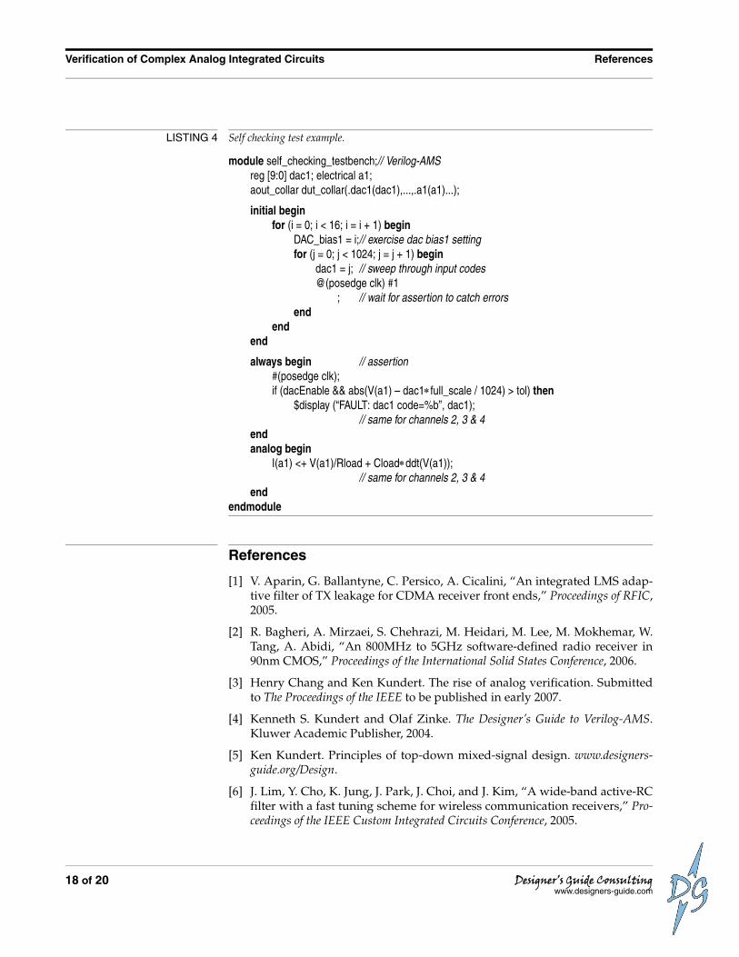
Listing 4 provides an example of a simple test. The test consists of stimu-lus to thoroughly exercise all the modes and settings of the functionalunit and an assertion to look for any errors. It should be noted that mostof the code written in the testbench is in standard Verilog “initial” and“always” blocks. In these cases the “analog” section is only used to setand add extra circuitry to the design.
With the verification, simulation, modeling plans and testbench devel-oped, the verification flow can be executed.
LISTING 2 Collar fragment that demonstrates using hierarchical references in the collar to reach into HDL model for real values.
module aout_collar (dac1, ..., a1, ...); // Collar for HDL model of DUTinput [9:0] dac1; logic [9:0] dac1;output a1; electrical a1;wor fault;assign fault = (a1_digital ===‘bz) || (a1_digital === ‘bx));
// assure line is connected
aout_hdl dut (.dac1(dac1_value), .a1(a1_digital), ...)// Instantiate DUT
analog V(a1) <+ dut.a1_real; // Grab the analog valueendmodule
module aout_hdl (dac1, ..., a1, ...); // Verilog model of DUTinput [9:0] dac1;output a1;real a1_real;assign a1 = ‘b1; // Indicate that output is connected
always @ (...) // condition such as the clocka1_real = dac1 ∗ full_scale / 1024;
endmodule
16 of 20 Designer’s Guide Consultingwww.designers-guide.com

Conclusion Verification of Complex Analog Integrated Circuits
5 Conclusion
Applying verification in A/RF design allows designers to continuedesigning more complex designs, try new architectures, and more rap-idly explore new circuit techniques. More science and thought is broughtto verifying the entire design, greatly reducing the risk of a chip failure.The efficiency of the design team is improved as new skills are broughtto the team. Designers can focus on meeting performance objectiveswhile verification engineers focus functional verification. Testbencheswritten by domain experts allow designers new to the design or designtypes to get up to speed quickly. A methodology based on modelingsmooths the growing communication issues between engineers. Finally,the models developed can also be used to help the test and product engi-neers for the IC.
This methodology is presented in considerably more detail in a paperthat is expected to be published in the Proceedings of the IEEE in early2007 [3].
LISTING 3 Collar fragments demonstrating how testbench can access signals completely contained within the DUT.
module self_checking_testbench; // Testbenchreal common_mode_voltage;aout_collar dut_collar (...) // instantiate the collarcommon_mode_voltage = V(dut_collar.cm_voltage);if (common_mode_voltage ...) ...// test the result
endmodule
module aout_collar (...) // Collar for the AHDL model of DUTreal cm_voltage;aout_ahdl dut (...) // instantiate the aout AHDL model
analog begincm_voltage = V(dut.dac1.common_mode_ref);
// hierarchical reference to the actual voltageend
endmodule
module aout_collar (...); // Collar for HDL model of DUTreal cm_voltage;aout_hdl dut (...) // instantiate the aout HDL modelalways @ (common_mode_control)// react to common mode control
cm_voltage = ...;// calculate directly based on control settingsendmodule
17 of 20Designer’s Guide Consultingwww.designers-guide.com
Verification of Complex Analog Integrated Circuits References
References
[1] V. Aparin, G. Ballantyne, C. Persico, A. Cicalini, “An integrated LMS adap-tive filter of TX leakage for CDMA receiver front ends,” Proceedings of RFIC,2005.
[2] R. Bagheri, A. Mirzaei, S. Chehrazi, M. Heidari, M. Lee, M. Mokhemar, W.Tang, A. Abidi, “An 800MHz to 5GHz software-defined radio receiver in90nm CMOS,” Proceedings of the International Solid States Conference, 2006.
[3] Henry Chang and Ken Kundert. The rise of analog verification. Submittedto The Proceedings of the IEEE to be published in early 2007.
[4] Kenneth S. Kundert and Olaf Zinke. The Designer’s Guide to Verilog-AMS.Kluwer Academic Publisher, 2004.
[5] Ken Kundert. Principles of top-down mixed-signal design. www.designers-guide.org/Design.
[6] J. Lim, Y. Cho, K. Jung, J. Park, J. Choi, and J. Kim, “A wide-band active-RCfilter with a fast tuning scheme for wireless communication receivers,” Pro-ceedings of the IEEE Custom Integrated Circuits Conference, 2005.
LISTING 4 Self checking test example.
module self_checking_testbench;// Verilog-AMSreg [9:0] dac1; electrical a1;aout_collar dut_collar(.dac1(dac1),...,.a1(a1)...);
initial beginfor (i = 0; i < 16; i = i + 1) begin
DAC_bias1 = i;// exercise dac bias1 settingfor (j = 0; j < 1024; j = j + 1) begin
dac1 = j; // sweep through input codes@(posedge clk) #1
; // wait for assertion to catch errorsend
endend
always begin // assertion#(posedge clk);if (dacEnable && abs(V(a1) – dac1∗full_scale / 1024) > tol) then
$display (“FAULT: dac1 code=%b”, dac1);// same for channels 2, 3 & 4
endanalog begin
I(a1) <+ V(a1)/Rload + Cload∗ddt(V(a1));// same for channels 2, 3 & 4
endendmodule
18 of 20 Designer’s Guide Consultingwww.designers-guide.com

References Verification of Complex Analog Integrated Circuits
[7] Andreas S. Meyer. Principles of Functional Verification. Elsevier Scientific,2003.
[8] K. Muhammad, et al, “A discrete time quad-band GSM/GPRS receiver in a90nm digital CMOS process,” Proceedings of the IEEE Custom Integrated Cir-cuits Conference, 2005.
[9] Y. Palaskas, et al, “A 5GHz class-AB power amplifier in 90nm CMOS withdigitally-assisted AM-PM correction,” Proceedings of the IEEE Custom Inte-grated Circuits Conference, 2005.
19 of 20Designer’s Guide Consultingwww.designers-guide.com

Verification of Complex Analog Integrated Circuits About The Authors
About The Authors
Ken Kundert. Ken has been at Designer’s Guide Consulting since 2005. From 1989 to2005, Ken worked at Cadence Design Systems as a Fellow. Ken created Spectre and wasthe principal architect of the Spectre circuit simulation family. As such, he has led thedevelopment of Spectre, SpectreHDL, and SpectreRF. He also played a key role in thedevelopment of Cadence's AMS Designer and made substantial contributions to both theVerilog-AMS and VHDL-AMS languages. While in school he authored Sparse, an indus-try standard sparse linear equation solver and created Agilent's harmonic balance simu-lator. Before that Ken was a circuit designer at Tektronix and Hewlett-Packard, andcontributed to the design of the HP 8510 microwave network analyzer. He has writtenthree books on circuit simulation: The Designer's Guide to Verilog-AMS in 2004, TheDesigner's Guide to SPICE and Spectre in 1995, and Steady-State Methods for Simulating Ana-log and Microwave Circuits in 1990; and created The Designer's Guide Community website.He has also authored eleven patents and over two-dozen papers published in refereedconferences and journals.
Ken received his Ph.D. in Electrical Engineering from the University of California at Ber-keley in 1989, his M.S. degree in 1983 and his B.S. in 1979.
Henry Chang. Henry has been at Designer’s Guide Consulting since 2005. From 1995 to2005, Henry worked at Cadence Design Systems, Inc. in research and development,methodology services, product marketing, corporate strategy, and in the office of theChief Technology Officer. He has also worked at Micro Linear and GE Lighting. He is theauthor of three books: Winning the SoC Revolution: Experiences in Real Design in 2003, Sur-viving the SoC Revolution: A Guide to Platform Based Design in 1999, and A Top-Down, Con-straint-Driven Design Methodology for Analog Integrated Circuits in 1997. He is on thesteering committee of the IEEE Custom Integrated Circuits Conference, serving pres-ently as the general chairman. He holds 10 US patents, has authored 14 technical papers,and has participated at conferences giving tutorials, sitting on panels, and giving key-note addresses.
Henry received his Ph.D. and M.S. in Electrical Engineering from the University of Cali-fornia at Berkeley in 1994 and 1992 respectively. He received his Sc.B. degree in ElectricalEngineering from Brown University in 1989.
About Designer’s Guide Consulting
We help design teams overcome difficult verification challenges. Those challenges caninvolve either functional or performance verification. A difficult functional verificationproblem might be assuring that a mixed-signal circuit consisting of tens or hundreds ofthousands of transistors with multiple ΔΣ converters operates correctly in each of itsthousands of distinct operating modes. A difficult performance verification might beassuring that a large behaviorally complex circuit meets some demanding specification,such as a SerDes operating with a bit-error rate of less than 10–18.
Designer’s Guide Consulting101 First Street, #150Los Altos, CA 94022+1 650-968-8291
20 of 20 Designer’s Guide Consultingwww.designers-guide.com