VERIFICATION OF BASIC LOGIC GATES · PDF fileEXPERIMENT: 1 DATE: VERIFICATION OF BASIC LOGIC...
33
EXPERIMENT: 1 DATE: VERIFICATION OF BASIC LOGIC GATES AIM: To verify the truth tables of Basic Logic Gates NOT, OR, AND, NAND, NOR, Ex-OR and Ex-NOR. APPARATUS: mention the required IC numbers, Connecting wires and IC Trainer Kit THEORY: Logic gates are the digital circuits with one output and one or more inputs. They are the basic building blocks of any logic circuit. Different logic gates are: AND, OR, NOT, NAND, NOR, Ex-OR and Ex-NOR They work according to certain logic. AND: The output of AND gate is true when the inputs A and B are True. Logic equation: B A Y . Truth Table: A B B A Y . 0 0 0 0 1 0 1 0 0 1 1 1 Graphic Symbol: OR: The output of OR gate is true when one of the inputs A and B or both the inputs are true.
-
Upload
nguyenkhanh -
Category
Documents
-
view
226 -
download
3
Transcript of VERIFICATION OF BASIC LOGIC GATES · PDF fileEXPERIMENT: 1 DATE: VERIFICATION OF BASIC LOGIC...

EXPERIMENT: 1 DATE:
VERIFICATION OF BASIC LOGIC GATES
AIM: To verify the truth tables of Basic Logic Gates
NOT, OR, AND, NAND, NOR, Ex-OR and Ex-NOR.
APPARATUS: mention the required IC numbers, Connecting wires and IC Trainer
Kit
THEORY:
Logic gates are the digital circuits with one output and one or more inputs. They
are the basic building blocks of any logic circuit.
Different logic gates are: AND, OR, NOT, NAND, NOR, Ex-OR and Ex-NOR
They work according to certain logic.
AND: The output of AND gate is true when the inputs A and B are True.
Logic equation: BAY .
Truth Table:
A B BAY .
0 0 0
0 1 0
1 0 0
1 1 1
Graphic Symbol:
OR: The output of OR gate is true when one of the inputs A and B or both the
inputs are true.

Logic equation: BAY
Truth Table:
A B BAY
0 0 0
0 1 0
1 0 0
1 1 1
Graphic Symbol:
NOT: The output of NOT gate is complement of the input.
Logic equation AY
Truth Table:
Graphic Symbol:
NAND: The output of NAND gate is true when one of the inputs or both the inputs
are low level.
Logic Equation: BABAY .
Truth Table:
Graphic Symbol:
NOR: The output of NOR gate is true when both the inputs are low.
Logic Equation: BABAY .
Truth Table:
Graphic Symbol:
EX-OR: The output of EX-OR gate is true when both the inputs are unequal.
Logic Equation: BABABAY
Truth Table:
Graphic Symbol:

EX-NOR: The output of EX-NOR gate is true when both the inputs are equal.
Logic Equation: BAABY
Truth Table:
Graphic Symbol:
PROCEDURE:
RESULT:

EXPERIMENT: 2 DATE:
REALIZATION GIVEN BOOLEAN FUNCTION
AIM: To simplify the given expression using K-map and realize it using Basic
gates and Universal gates.
APPARATUS:( write the apparatus)
THEORY:
Canonical Forms (Normal Forms): Any Boolean function can be written in
disjunctive normal form (sum of min-terms) or conjunctive normal form (product
of max-terms). A Boolean function can be represented by a Karnaugh map in
which each cell corresponds to a minterm. The cells are arranged in such a way
that any two immediately adjacent cells correspond to two minterms of distance
1. There is more than one way to construct a map with this property.
Karnaugh Maps:
Two- variable K-Map
Three Variable K-Map:
Four variable K-Map:
Any two adjacent squares in the map differ by only one variable, which is
primed in one square and unprimed in the other. Therefore, any two minterms in
djacent squares (vertically or horizontally, but not diagonally, adjacent) that are
ORed together will cause a removal of the dissimilar variable.
Simplification of given expression using K-Map:
Given expression is
K-Map:
)14,11,10,9,8,6,2(),,,( DCBAF

Simplified Expression is :
Realization using Basic gates:
Realization using NAND gates:
PROCEDURE: 1. Simplify the given Boolean expression using 4 Variable K-Map to minimize the
number of literals in the given expression. 2. Design Logic circuit using Basic gates. 3. Check the components for their working. 4. Insert the appropriate IC into the IC base. 5. Make connections as shown in the circuit diagram.

6. Provide the input data via the input switches and observe the output on output LEDs
RESULT:

EXPERIMENT: 3 DATE:
REALIZATION OF BASIC GATES USING NAND
AIM: To implement the basic gates(NOT, AND and OR), Ex-OR and Ex-NOR using
universal NAND gates.
APPARATUS:
THEORY:
AND, OR, NOT are called basic gates as their logical operation cannot be
simplified further. NAND and NOR are called universal gates as using only NAND
or only NOR any logic function can be implemented. Using NAND and NOR gates
and De Morgan's Theorems different basic gates & EX-OR gates are realized.
NAND : The output of NAND gate is true when one of the inputs or both the
inputs are low level.
Logic Equation: BABAY .
Truth Table:
A B BABAY .
0 0 1
0 1 1
1 0 1
1 1 0
Graphic Symbol:
AND-Invert Invert-OR

Realization of basic gates using NAND:
PROCEDURE:
1. Check the components for their working. 2. Insert the appropriate IC into the IC base. 3. Make connections as shown in the circuit diagram. 4. Provide the input data via the input switches and observe the output on
output LEDs RESULT:

EXPERIMENT: 4 DATE:
REALIZATION OF BASIC GATES USING NOR
AIM: To implement the basic gates(NOT, AND and OR), Ex-OR and Ex-NOR using
universal NOR gates.
APPARATUS:
THEORY:
AND, OR, NOT are called basic gates as their logical operation cannot be
simplified further. NAND and NOR are called universal gates as using only NAND
or only NOR any logic function can be implemented. Using NAND and NOR gates
and De Morgan's Theorems different basic gates & EX-OR gates are realized.
NOR : The output of NOR gate is true when both the inputs are low.
Logic Equation: BABAY .
Truth Table:
A B BABAY .
0 0 1
0 1 0
1 0 0
1 1 0
Graphic Symbol:
OR-Invert Invert-AND

Realization of basic gates using NOR:
PROCEDURE:
1. Check the components for their working. 2. Insert the appropriate IC into the IC base. 3. Make connections as shown in the circuit diagram. 4. Provide the input data via the input switches and observe the output on
output LEDs RESULT:

EXPERIMENT: 5 DATE:
DESIGN OF HALF ADDER AND HALF SUBTRACTOR
AIM: To design Half-Adder and Half Subtractor using basic logic gates and verification of truth table.
APPARATUS: THEORY: Half-Adder:
A combinational logic circuit that performs the addition of two data bits, A and B, is called a half-adder. Addition will result in two output bits; one of which is the sum bit, S, and the other is the carry bit, C.
The Boolean functions describing the half-adder are:
S =A B C = A B
Half-Subtractor:
Subtracting a single-bit binary value B from another A (i.e. A -B)
produces a difference bit D and a borrow out bit B-out. This operation is called
half subtraction and the circuit to realize it is called a half subtractor.
The Boolean functions describing the half-Subtractor are:
B_out =A B D = A’ B

Realization of Half Adder Circuit:

Realization of Half-Subtractor Circuit:
PROCEDURE: 1. Check the components for their working. 2. Insert the appropriate IC into the IC base. 3. Make connections as shown in the circuit diagram. 4. Provide the input data via the input switches and observe the output on output LEDs
RESULT:

EXPERIMENT: 6 DATE:
DESIGN OF FULL ADDER AND FULL SUBTRACTOR
AIM: To design Full-Adder and Full-Subtractor using basic logic gates and
verification of truth table.
APPARATUS:
THEORY:
Full-Adder:
The half-adder does not take the carry bit from its previous stage into account. This carry bit from its previous stage is called carry-in bit. A combinational logic circuit that adds two data bits, A and B, and a carry-in bit, Cin , is called a full-adder.
The Boolean functions describing the full-adder are:
S =A B Cin
C=AB+BCin+CinAFull Subtractor:
Subtracting two single-bit binary values, B, Cin from a single-bit value A produces a difference bit D and a borrow out Br bit. This is called full subtraction.
The Boolean functions describing the full-subtractor are:
D = A B Cin
Br= A'B+BCin+CinA'

Realization of Full-Adder:
With basic Gates:

Realization of Full-Subtractor:
PROCEDURE:
1. Check the components for their working. 2. Insert the appropriate IC into the IC base. 3. Make connections as shown in the circuit diagram. 4. Provide the input data via the input switches and observe the output on output LEDs
RESULT:

EXPERIMENT: 7 DATE:
BINARY TO GRAY CODE CONVERTER
AIM: To design Binary to Gray code converter and verification of truth table.
APPARATUS:
THEORY:
Code converter is a combinational circuit that translates the input code word into
a new corresponding word.
Gray Code is one of the most important codes. It is a non-weighted code
which belongs to a class of codes called minimum change codes. In this codes
while traversing from one step to another step only one bit in the code group
changes. In case of Gray Code two adjacent code numbers differs from each other
by only one bit. The idea of it can be cleared from the table given below. As this
code it is not applicable in any types of arithmetical operations but it has some
applications in analog to digital converters and in some input/output devices.

Binary to Gray Code Conversion Table:
Decimal Number
0
1
2
3
4
5
6
7
8
9
10
11
12
13
14
15

Binary to Gray Code Conversion from Conversion Table:
Realization Binary to Gray Code Converter Using Ex-OR Gates:

Realization of Binary to Gray Code Converter Using NAND Gates:
PROCEDURE:
1. Construct Binary to Gray code Conversion table as shown in Table. 2. Deriver Boolean Expression for each output variables(G0,G1,G2 and G3). 3. Check the components for their working. 4. Insert the appropriate IC into the IC base. 5. Make connections as shown in the circuit diagram. 6. Provide the input data via the input switches and observe the output on
output LEDs RESULT:

EXPERIMENT: 8 DATE:
DESIGN OF MULTIPLEXER CIRCUIT
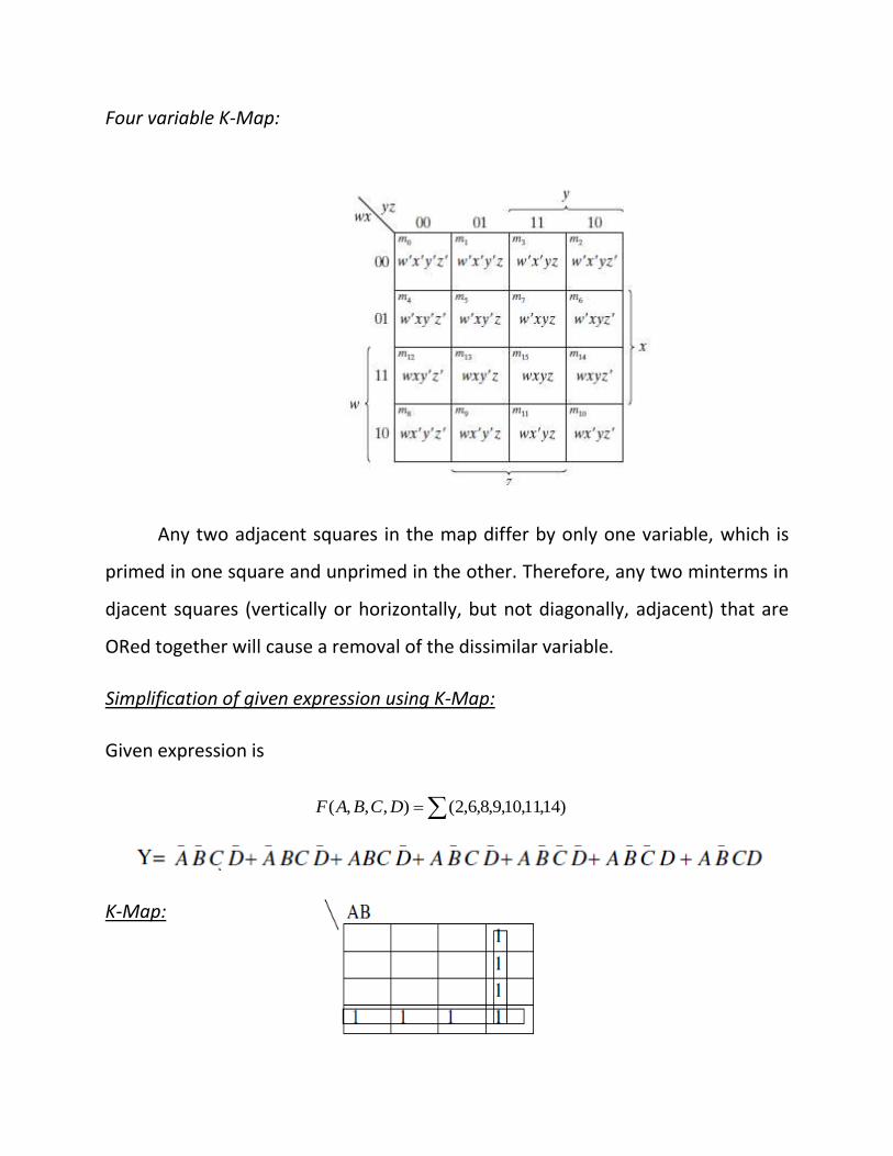
AIM: To design a combinational circuit for 4X1 Multiplexer using NAND gates
and verify the truth table
APPARATUS:
THEORY:
Multiplexers are very useful components in digital systems. They transfer a
large number of information units over a smaller number of channels, (usually
one channel) under the control of selection signals. Multiplexer means many to
one. A multiplexer is a circuit with many inputs but only one output. By using
control signals (select lines) we can select any input to the output. Multiplexer is
also called as data selector because the output bit depends on the input data bit
that is selected. The general multiplexer circuit has 2n input signals, n
control/select signals and 1 output signal.

The 4X1 multiplexer comprises 4-input bits, 1- output bit, and 2- Selection
lines. The four input bits are namely D0, D1, D2 and D3, respectively; only one of
the input bit is transmitted to the output. The out ‘q’ depends on the value of
selection input AB. The selection bit pattern AB decides which of the input data
bit should transmit the output. The following figure shows the 4X1 multiplexer
circuit diagram using AND gates. For example, when the control bits AB =00, then
the higher AND gate are allowed while remaining AND gates are restricted. Thus,
data input D0 is transmitted to the output ‘q”
Input Selection Table:
A B Output(q)
0 0 D0
0 1 D1
1 0 D2
1 1 D3
Realization of 4X1 Multiplexer using Basic gates:
Realization of 4X1 Multiplexer using NAND gates with Enable Input :
PROCEDURE:
1. Check the components for their working. 2. Insert the appropriate IC into the IC base. 3. Make connections as shown in the circuit diagram. 4. Provide the input data via the input switches and observe the output on
output LEDs
RESULT:

EXPERIMENT: 9 DATE:
DESIGN OF DEMULTIPLEXER CIRCUIT
AIM: To design a combinational circuit for 1X4 Demultiplexer and verify its truth
table.
APPARATUS:
THEORY:
De-multiplexers perform the opposite function of multiplexers. They
transfer a small number of information units (usually one unit) over a larger
number of channels under the control of selection signals. The general de-
multiplexer circuit has 1 input signal, n control/select signals and 2n output
signals. De-multiplexer circuit can also be realized using a decoder circuit with
enable.
Truth Table for 1X4 Demultiplexer using Enable Input:

Realization of 1X4 Demultiplexer using Enable Input
PROCEDURE:
1. Check the components for their working. 2. Insert the appropriate IC into the IC base. 3. Make connections as shown in the circuit diagram. 4. Provide the input data via the input switches and observe the output on
output LEDs
RESULT:

EXPERIMENT:10 DATE:
DESIGN OF FLIPFLOPS
AIM: To Construct the basic SR and D Flip-Flips and verify their truth tables.
APPARATUS:
THEORY:
Logic circuits that incorporate memory cells are called sequential logic
circuits; their output depends not only upon the present value of the input but
also upon the previous values. Sequential logic circuits often require a timing
generator (a clock) for their operation. The latch (flip-flop) is a basic bi-stable
memory element widely used in sequential logic circuits. Usually there are two
outputs, Q and its complementary value. Some of the most widely used latches
are listed below.
SR LATCH:
An S-R latch consists of two cross-coupled NOR gates. An S-R flip-flop can
also be design using cross-coupled NAND gates as shown. The truth tables of the
circuits are shown in the figures.
A clocked S-R flip-flop has an additional clock input so that the S and R
inputs are active only when the clock is high. When the clock goes low, the state
of flip-flop is latched and cannot change until the clock goes high again.
Therefore, the clocked S-R flip-flop is also called “enabled” S-R flip-flop.

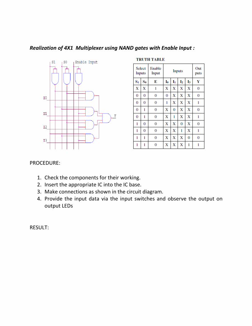
A D latch combines the S and R inputs of an S-R latch into one input by
adding an inverter. When the clock is high, the output follows the D input, and
when the clock goes low, the state is latched.
SR Latch:
SR Latch with NOR gates
SR Latch with NAND gates
SR Flip Flop
Functional Table of SR Flip flop:
Excitation Table for SR FF:
D(Delay) -Flip Flop:
Functional Table of D- Flip flop:

Excitation Table for D- FF:
PROCEDURE:
1. Check the components for their working. 2. Insert the appropriate IC into the IC base. 3. Make connections as shown in the circuit diagram. 4. Provide the input data via the input switches and observe the output on
output LEDs
RESULT:

EXPERIMENT:10 DATE:
DESIGN OF DECODERS AIM: To design 2x4 Decoder circuit using basic logic gates and verify its truth table APPARATUS: THEORY: A decoder is a combinational circuit that connects the binary information from ‘n’ input lines to a maximum of 2n unique output lines. Decoder is also called a min-term generator/maxterm generator. A min-term generator is constructed using AND and NOT gates. The appropriate output is indicated by logic 1 (positive logic). Max-term generator is constructed using NAND gates. The appropriate output is indicated by logic 0 (Negative logic). 2:4 DECODER (MIN TERM GENERATOR): Truth Table:

Realization of 2X4 Decoder using basic gates:
2:4 DECODER (MAX TERM GENERATOR): Truth Table:

PROCEDURE: 1. Check the components for their working. 2. Insert the appropriate IC into the IC base. 3. Make connections as shown in the circuit diagram. 4. Provide the input data via the input switches and observe the output on
output LEDs RESULT:
![Gates and Logic: From Transistors to Logic Gates and Logic ......Gates and Logic: From Transistors to Logic Gates and Logic Circuits [Weatherspoon, Bala, Bracy, and Sirer] Prof. Hakim](https://static.fdocuments.in/doc/165x107/5fa95cb6eb1af8231472f381/gates-and-logic-from-transistors-to-logic-gates-and-logic-gates-and-logic.jpg)