Vector Processing as a Soft Processor Acceleratorlemieux/publications/yu-trets2009prepress.pdf ·...
31
Vector Processing as a Soft Processor Accelerator JASON YU, CHRISTOPHER EAGLESTON, CHRISTOPHER HAN-YU CHOU, MAXIME PERREAULT and GUY LEMIEUX University of British Columbia Current FPGA soft processor systems use dedicated hardware modules or accelerators to speed up data-parallel applications. This work explores an alternative approach of using a soft vector processor as a general-purpose accelerator. The approach has the benefits of a purely software- oriented development model, a fixed ISA allowing parallel software and hardware development, a single accelerator that can accelerate multiple applications, and scalable performance from the same source code. With no hardware design experience needed, a software programmer can make area-versus-performance tradeoffs by scaling the number of functional units and register file bandwidth with a single parameter. A soft vector processor can be further customized by a number of secondary parameters to add or remove features for a specific application to optimize resource utilization. This paper introduces VIPERS, a soft vector processor architecture that maps efficiently into an FPGA and provides a scalable amount of performance for a reasonable amount of area. Compared to a Nios II/s processor, instances of VIPERS with 32 processing lanes achieve up to 44× speedup using up to 26× the area. Categories and Subject Descriptors: C.1.2 [Processor Architectures]: Multiple Data Stream Architectures (Mul- tiprocessors)—array and vector processors, single-instruction-stream, multiple-data-stream processors (SIMD) General Terms: Measurement, Performance, Design Additional Key Words and Phrases: computer architecture, embedded processor, multimedia processing, parallelism, soft processor, vector processor 1. INTRODUCTION Soft-core processors such as MicroBlaze [Xilinx, Inc. 2008] help simplify control- intensive system design because software programming is far easier than hardware design. This shortens time-to-market and shrinks development costs. However, the amount of compute performance available from soft-core processors is strictly limited. For example, the highest-performing Nios II [Altera Corp. 2008c] soft processor uses a single-issue, in-order RISC pipeline. Many embedded applications such as those found in [EEMBC 2008] have plenty of data-level parallelism available, but they are performance-limited by the processor design itself. This research was funded by NSERC and Altera. Authors’ Addresses: Guy Lemieux, Electrical and Computer Engineering, The University of British Columbia, 5500–2332 Main Mall, Vancouver, BC, V6T 1Z4, Canada. Permission to make digital/hard copy of all or part of this material without fee for personal or classroom use provided that the copies are not made or distributed for profit or commercial advantage, the ACM copyright/server notice, the title of the publication, and its date appear, and notice is given that copying is by permission of the ACM, Inc. To copy otherwise, to republish, to post on servers, or to redistribute to lists requires prior specific permission and/or a fee. c 2009 ACM 0000-0000/2009/0000-0001 $5.00 ACM Journal Name, Vol. 0, No. 0, February 2009, Pages 1–31.
Transcript of Vector Processing as a Soft Processor Acceleratorlemieux/publications/yu-trets2009prepress.pdf ·...

Vector Processing as a Soft Processor Accelerator
JASON YU, CHRISTOPHER EAGLESTON,
CHRISTOPHER HAN-YU CHOU, MAXIME PERREAULT
and
GUY LEMIEUX
University of British Columbia
Current FPGA soft processor systems use dedicated hardware modules or accelerators to speedup data-parallel applications. This work explores an alternative approach of using a soft vector
processor as a general-purpose accelerator. The approach has the benefits of a purely software-oriented development model, a fixed ISA allowing parallel software and hardware development,a single accelerator that can accelerate multiple applications, and scalable performance from thesame source code. With no hardware design experience needed, a software programmer canmake area-versus-performance tradeoffs by scaling the number of functional units and registerfile bandwidth with a single parameter. A soft vector processor can be further customized by anumber of secondary parameters to add or remove features for a specific application to optimizeresource utilization. This paper introduces VIPERS, a soft vector processor architecture thatmaps efficiently into an FPGA and provides a scalable amount of performance for a reasonableamount of area. Compared to a Nios II/s processor, instances of VIPERS with 32 processing lanesachieve up to 44× speedup using up to 26× the area.
Categories and Subject Descriptors: C.1.2 [Processor Architectures]: Multiple Data Stream Architectures (Mul-
tiprocessors)—array and vector processors, single-instruction-stream, multiple-data-stream processors (SIMD)
General Terms: Measurement, Performance, Design
Additional Key Words and Phrases: computer architecture, embedded processor, multimediaprocessing, parallelism, soft processor, vector processor
1. INTRODUCTION
Soft-core processors such as MicroBlaze [Xilinx, Inc. 2008] help simplify control-
intensive system design because software programming is far easier than hardware design.
This shortens time-to-market and shrinks development costs. However, the amount of
compute performance available from soft-core processors is strictly limited. For example,
the highest-performing Nios II [Altera Corp. 2008c] soft processor uses a single-issue,
in-order RISC pipeline. Many embedded applications such as those found in [EEMBC
2008] have plenty of data-level parallelism available, but they are performance-limited by
the processor design itself.
This research was funded by NSERC and Altera. Authors’ Addresses: Guy Lemieux, Electrical and Computer
Engineering, The University of British Columbia, 5500–2332 Main Mall, Vancouver, BC, V6T 1Z4, Canada.
Permission to make digital/hard copy of all or part of this material without fee for personal or classroom use
provided that the copies are not made or distributed for profit or commercial advantage, the ACM copyright/server
notice, the title of the publication, and its date appear, and notice is given that copying is by permission of the
ACM, Inc. To copy otherwise, to republish, to post on servers, or to redistribute to lists requires prior specific
permission and/or a fee.
c© 2009 ACM 0000-0000/2009/0000-0001 $5.00
ACM Journal Name, Vol. 0, No. 0, February 2009, Pages 1–31.
2 · J. Yu, C. Eagleston, C. Chou, M. Perreault and G. Lemieux
P C
I DA L U
I n s t r u c t i o n
M e m o r y 3 2
S c a l a r C o r e
M e m o r y
C r o s s b a r s
M e m o r y U n i t
F I F O q u e u e
1 W r i t e p o r t
2 R e a d p o r t s
V e c t o r L a n e
M a i n
M e m o r y
1 2 8
I D
I D
V e c t o r L a n e
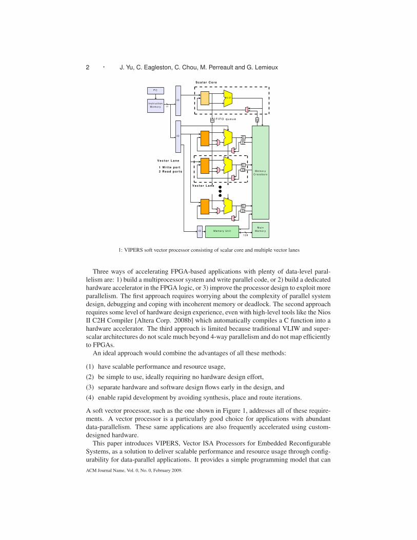
1: VIPERS soft vector processor consisting of scalar core and multiple vector lanes
Three ways of accelerating FPGA-based applications with plenty of data-level paral-
lelism are: 1) build a multiprocessor system and write parallel code, or 2) build a dedicated
hardware accelerator in the FPGA logic, or 3) improve the processor design to exploit more
parallelism. The first approach requires worrying about the complexity of parallel system
design, debugging and coping with incoherent memory or deadlock. The second approach
requires some level of hardware design experience, even with high-level tools like the Nios
II C2H Compiler [Altera Corp. 2008b] which automatically compiles a C function into a
hardware accelerator. The third approach is limited because traditional VLIW and super-
scalar architectures do not scale much beyond 4-way parallelism and do not map efficiently
to FPGAs.
An ideal approach would combine the advantages of all these methods:
(1) have scalable performance and resource usage,
(2) be simple to use, ideally requiring no hardware design effort,
(3) separate hardware and software design flows early in the design, and
(4) enable rapid development by avoiding synthesis, place and route iterations.
A soft vector processor, such as the one shown in Figure 1, addresses all of these require-
ments. A vector processor is a particularly good choice for applications with abundant
data-parallelism. These same applications are also frequently accelerated using custom-
designed hardware.
This paper introduces VIPERS, Vector ISA Processors for Embedded Reconfigurable
Systems, as a solution to deliver scalable performance and resource usage through config-
urability for data-parallel applications. It provides a simple programming model that can
ACM Journal Name, Vol. 0, No. 0, February 2009.

Vector Processing as a Soft Processor Accelerator · 3
be easily understood by software developers, and its application-independent architecture
allows hardware and software development to be separated. A single vector unit can accel-
erate multiple applications. Also, unlike many C-to-hardware flows, modifications to an
accelerated function simply require a software compile; there is no need to place and route
again.
A soft vector processor from VIPERS can easily exploit the configurability of FPGAs by
customizing the amount of parallelism, feature set, and instruction support needed by the
application. Customization extends to a flexible memory interface, which can be tailored to
the required data access granularity. This opens a rich design space to the user and allows
greater area/performance tradeoffs than current soft processor solutions, yet it is simple
enough that software programmers can understand the tradeoffs.
An earlier version of this work appeared as [Yu et al. 2008]. This paper repre-
sents a significant extension of that work, presenting more details on C2H, the vec-
tor execution model, vector memory interface design, vector pipeline organization, im-
proved vector assembly code for all three benchmarks, and fully unrolled median fil-
ter and motion estimation vector code that is up to 5x faster. The performance model
has been expanded and altered to portray the current vector processor implementation
rather than a more ideal implementation. Performance results of the vector processor
are now based on cycle-accurate Verilog simulations using ModelSim rather than the
performance model. Also, two new tables demonstrate control over the amount of used
resources by varying the soft processor parameters. Full vector ISA details are avail-
able in [Yu 2008]. The processor, assembler, and benchmark code are available online
at http://www.ece.ubc.ca/∼lemieux/downloads.
2. BACKGROUND AND PREVIOUS WORK
Vector processing has been used in supercomputers for scientific tasks for over three
decades. Modern supercomputing systems like the Earth Simulator [Habata et al. 2003]
and Cray X1 are based on single-chip vector processors. The following sections give an
overview of vector processing, and the current solutions for improving the performance
of soft processors and accelerating FPGA-based applications according to the categories
introduced in Section 1.
2.1 Vector Processing Overview
The vector processing model operates on vectors of data. Each vector operation specifies
an identical operation on the individual data elements of the source vectors, producing an
equal number of independent results. This also makes it a natural method to exploit data-
level parallelism, which has the same properties. Vector processors use pipelining and
multiple parallel datapaths—called vector lanes—to reduce execution time. For a more
detailed description of classical vector architectures, please see [Hwang and Briggs 1984].
2.1.1 Vector Instruction Set Architecture. A vector architecture contains a vector unit
and a separate scalar unit. The scalar unit is needed to execute non-vectorizable portions of
the code, and most control flow instructions. The scalar unit can also broadcast operands
to all vector lanes, such as adding a constant to a vector.
The vector unit performs loop-like operations by repeating a single operation to all vec-
tor elements. Vector instructions are controlled by a vector length (VL) register, which
specifies the number of elements within the vector to operate on. This vector length reg-
ACM Journal Name, Vol. 0, No. 0, February 2009.

4 · J. Yu, C. Eagleston, C. Chou, M. Perreault and G. Lemieux
ister can be modified on a per-instruction basis. Applications are usually written to be
aware of the maximum VL (MVL) of the processor on which it is running. This saves
significant overhead on tight looping operations, since there is no need for increment and
compare/branch instructions each iteration.
Vector performance also relies upon good memory performance, so it is important to
have a rich set of vector load and store instructions. Vector addressing modes can effi-
ciently scatter or gather entire vectors of data to and from memory. The three primary
vector addressing modes are: unit stride, constant stride, and indexed addressing. Unit
stride accesses data elements in adjacent memory locations, constant stride accesses data
elements in memory with a constant size separation between elements, and indexed ad-
dressing accesses data elements by adding a variable offset for each element to a common
base address. After a vector memory access, the address base register can also be auto-
incremented by a constant amount.
2.1.2 Example. Consider the 8-tap finite impulse response (FIR) filter,
y[n] =
7∑
k=0
x[n − k]h[k].
This can be implemented in Nios II assembly language where 65 instructions are executed
per result.
The same FIR filter implemented for VIPERS is shown in Figure 2. Some initialization
instructions are omitted for brevity. The vector code computes a single result by multiply-
ing all coefficients with data samples using just the vmac/vcczacc instruction pair. To
prepare for the next result, data samples are shifted by one vector element position. A total
of 10 instructions (from the “.L5” label to the “bne r11, r6, .L5” branch) are executed per
result. Scaling the FIR filter to 64 filter taps requires executing 458 Nios II instructions;
the VIPERS approach requires executing the same 10 instructions with a vector length of
64 elements.
Most VIPERS instructions are based upon the VIRAM instruction set [Kozyrakis and
Patterson 2003b]. However, the three capitalised instructions in Figure 2 are unique to
VIPERS and replace a sequence of eight VIRAM instructions. These instructions uti-
lize FPGA resources to speed up multiply-accumulate, vector reduction (summation), and
adjacent-element shifting. These features are described in more detail in Section 3.4.
2.2 Related Vector Work
A number of single-chip and FPGA-based vector processors are described in the following
sections. Closely related is vector-inspired SIMD processing, which is widely used in
multimedia instruction extensions found in mainstream microprocessors.
2.2.1 SIMD Extensions. SIMD extensions such as Intel SSE [Thakkur and Huff 1999]
and PowerPC AltiVec [Diefendorff et al. 2000] are oriented towards short, fixed-length
vectors. An entire SIMD vector register is typically 128 bits long and can be divided into
8, 16 or 32 bit wordlengths, allowing vector lengths to range from 4 to 16 elements. SIMD
instructions operate on these short vectors, and each instruction typically executes in a sin-
gle cycle. In general, SIMD extensions lack support for strided memory access patterns
and more complex memory manipulation instructions, hence they must devote many in-
structions to address transformation and data manipulation to support the instructions that
ACM Journal Name, Vol. 0, No. 0, February 2009.

Vector Processing as a Soft Processor Accelerator · 5
movi r12, N ; Total samples to process
movi r6, NTAPS ; Number of filter taps
vld v2, vbase1 ; Load filter coefficients once
vmstc vinc0, r6 ; Set auto−increment to NTAPS
vmstc vindex, zero ; Set vindex to 0 for vext 5
.L4:
movi r11, 2*NTAPS ; Window size of samples to load
vmstc VL, r11 ; Set VL to window size
vld v1,vbase0,vinc0 ; Load & advance x[ ] input buffer
.L5: 10
vmstc VL, r6 ; Reset VL to number of taps
VMAC v1, v2 ; Mult.−accum. VL values, then set VL to 1
VCCZACC v3 ; Copy accum. result to v3 and clear accum.
vext.vs r3, v3 ; Extract scalar sum from v3[vindex]
stw r3, 0(r10) ; Store FIR result to y[ ] output buffer 15
addi r10, r10, 4 ; Increment y[ ] buffer position
vmstc VL, r11 ; Reset VL to number of window size
VUPSHIFT v1, v1 ; Shift remaining vector elems by 1 position
addi r11, r11, −1
bne r11, r6, .L5 20
sub r12, r12, r6 ; Done computing NTAPS total FIR results
bne r12, zero, .L4 ; Process remaining input
2: VIPERS soft vector processor assembly code for 8-tap FIR filter
do the actual computation [Talla and John 2001].
2.2.2 Single-chip Vector Processors. Torrent T0 [Asanovic 1998] and VIRAM
[Kozyrakis and Patterson 2003b] are single-chip vector microprocessors implemented as
custom ASICs that support a complete vector architecture. The T0 vector unit attaches as
a co-processor to a MIPS scalar unit. The vector unit has 16 vector registers, a maximum
vector length of 32, and 8 parallel vector lanes. VIRAM is implemented in 0.18 µm tech-
nology and runs at 200MHz. It has 32 registers, a 16-entry vector flag register file, and two
ALUs replicated over 4 parallel vector lanes. These two vector processors share the most
similarity in architecture to this work.
2.2.3 FPGA-based Vector Processors. Vector processors have been implemented in
FPGAs as an ASIC prototype [Casper et al. 2005] and as an application-specific solu-
tion [Hasan and Ziavras 2005]. Five additional implementations specifically designed for
FPGAs are described below.
The first, [Cho et al. 2006], is designed for Xilinx Virtex-4 SX and operates at 169MHz.
It contains 16 processing lanes, each 16-bits wide, and 17 on-chip memory banks con-
nected to a MicroBlaze processor through fast simplex links (FSL). It is not clear how
many vector registers are supported. Compared to MicroBlaze, speedups of 4–10× are
demonstrated with four applications (FIR, IIR, matrix multiply, and 8×8 DCT). The pro-
cessor implementation seems fairly complete.
The second, [Jacob et al. 2006], is a soft vector processor for biosequence applications.
ACM Journal Name, Vol. 0, No. 0, February 2009.

6 · J. Yu, C. Eagleston, C. Chou, M. Perreault and G. Lemieux
It contains an instruction controller that executes control flow instructions and broadcasts
vector instructions to an array of 16-bit wide processing elements. Details are scarce, but
it seems to have limited features and few instructions. Like this work, it also argues for a
soft vector processor core.
The third, [Yang et al. 2007], consists of two identical vector processors located on
two Xilinx XC2V6000 FPGA chips. Each 70MHz processor contains a simplified scalar
core with 16 instructions. The vector part consists of 8 vector registers, 8 lanes (each
containing a 32-bit floating-point unit), and supports a maximum vector length (MVL) of
64. Eight vector instructions are supported: vector load/store, vector indexed load/store,
vector-vector and vector-scalar multiplication/addition. However, only matrix multiplica-
tion was demonstrated on the system.
The fourth, [Chen et al. 2008], is a floating-point vector unit based on T0 that operates
at 189MHz on a Xilinx Virtex II Pro device. It has 16 vector registers of 32 bits, a vector
length of 16, and 8 vector lanes. Three functional units are implemented: floating-point
adder, floating-point multiplier, and vector memory unit that interfaces to a 256-bit memory
bus. No control processor is included for non-floating-point or memory instructions, and it
is unclear whether addressing modes other than unit-stride access are implemented.
The fifth, VESPA [Yiannacouras et al. 2008], closely follows VIRAM but is optimized
for FPGA implementation. It is based on a custom MIPS-compatible scalar core, supports
fine-grained instruction subsetting, and uses on-chip cache and off-chip SDRAM memory.
The VESPA implementation is very similar in area use and clock speed to VIPERS. In
contrast, VIPERS is less strict about VIRAM compliance, so it offers double the vector
registers and several new instructions to take advantage of FPGA resources.
2.3 Alternatives for Accelerating Data-Parallel Applications
Alternative methods for accelerating data-parallel applications are: multiprocessor sys-
tems, custom-designed and synthesized hardware accelerators, and other soft processor
architectures. The following sections describe these alternatives in more detail.
2.3.1 Multiprocessor Systems. The parallelism in multiprocessor systems can be de-
scribed as multiple instruction multiple data (MIMD) or single instruction multiple data
(SIMD). Each processor in a MIMD system has its own instruction memory, executes its
own instruction stream, and operates on different data. In contrast, a SIMD system has a
single instruction stream that is shared by all processors. For example, the vector processor
in this paper is a type of SIMD system.
Although SIMD systems are almost always homogeneous, MIMD systems can be het-
erogeneous. In particular, FPGAs make it easy to create MIMD systems that can acceler-
ate heterogeneous workloads (e.g., multi-programming) that otherwise do not parallelize
easily. Specialized systems with unique architectures can be designed to exploit the char-
acteristics of a particular application for better performance. For example, the IPv4 packet
forwarding system in [Ravindran et al. 2005] has 14 MicroBlaze processors and two hard
core PowerPC processors arranged in four parallel processor pipelines with each stage
performing a specific task.
2.3.2 Custom-designed Hardware Accelerators. Soft processors often use hardware
accelerators to speed up certain portions of an application. Traditionally, these acceler-
ators are designed manually in HDL by a hardware designer. The interface between the
soft processor and the accelerator can vary, but generally falls into two categories. Custom
ACM Journal Name, Vol. 0, No. 0, February 2009.

Vector Processing as a Soft Processor Accelerator · 7
instruction accelerators are custom logic blocks within the processor’s datapath, mapped
to special opcodes in the processor’s ISA. They can directly access the processor’s register
file, and effectively extend the functionality of the processor’s ALU. Coprocessor acceler-
ators are decoupled from the main processor, ideally allowing the CPU and the accelerator
to execute concurrently. They can also have direct access to memory.
2.3.3 Synthesized Hardware Accelerators. Modern behavioral synthesis techniques
can automatically create hardware accelerators from software. In particular, synthesiz-
ing circuits from C has long been advocated due to its widespread use in embedded de-
signs. Like custom-designed hardware accelerators, they can be divided into two cate-
gories: ASIPs and synthesized coprocessors.
Application-specific instruction set processors (ASIPs) usually focus on the ASIC mar-
ket, but recent research targets soft processors as well [Dinh et al. 2008]. ASIPs have
configurable instruction sets that allow the user to extend the processor by adding custom
instructions to replace common code sequences. An important goal is automatic generation
of the custom instructions from benchmark software. This frequently requires the use of
proprietary synthesis languages and compilers. The Tensilica Xtensa [Tensilica Inc. 2008]
and ARC Core processors [ARC International 2008] are two commercial examples.
The Nios II C2H Compiler [Altera Corp. 2008b] automatically synthesizes a single C
function into a hardware accelerator. It is automatically connected to a Nios II memory
system through the Avalon system fabric [Altera Corp. 2008a]. Figure 3 shows a Nios II
system with one C2H accelerator and connections between the various components of
the system. The C2H compiler synthesizes pipelined hardware from the C source code
using parallel scheduling and direct memory access. Each C assignment statement infers
a pipeline register. Loops are automatically pipelined and scheduled, but not unrolled; this
must be done manually. Initially, each C memory reference is handled by creating its own
master port in the accelerator hardware. Normally, when several master ports connect to the
same memory block, the Avalon system fabric creates an arbiter to serialize accesses. As
an additional optimization, C2H automatically merges all its own master ports connected
to the same memory block by combining the references and scheduling them internally.
Some other C-based/C-like languages or synthesis tools include Carte by SRC Comput-
ers, Catapult C Synthesis by Mentor Graphics, CHiMPS by Xilinx, Cynthesizer by Forte,
Dime-C by Nallatech, Handel-C by Celoxica, Impulse C by Impulse Accelerated Tech-
nologies, Mitrion-C by Mitrionics, PICO Express by Synfora, NAPA C by National Semi-
conductor and SA-C by Colorado State University, Streams-C by Los Alamos National
Laboratory, and SystemC by the Open SystemC Initiative.
2.3.4 Soft Processor Architectures. VLIW and superscalar architectures have also
been used in FPGAs for acceleration [Grabbe et al. 2003; Brost et al. 2007; Jones et al.
2005; Saghir et al. 2006]. These designs offer increased parallelism, typically up to about
4 functional units. FPGAs have also been used to prototype VLIW and superscalar archi-
tectures intended for full-custom implementation, but they tend to be inefficient in area and
performance [Lu et al. 2007; Ray and Hoe 2003].
2.3.5 Drawbacks. The acceleration methods described above each have significant
drawbacks. Multiprocessor systems are very flexible, but are complex both to design and
use. Significant hardware knowledge is needed to design a multiprocessor system, includ-
ing consideration of issues such as interconnect, memory architecture, cache coherence
ACM Journal Name, Vol. 0, No. 0, February 2009.

8 · J. Yu, C. Eagleston, C. Chou, M. Perreault and G. Lemieux
C 2 H
A c c e l e r a t o r
C o n t r o l
A r b i t e r A r b i t e r
A v a l o n
F a b r i c
N i o s I I
P r o c e s s o r
I n s t r u c t i o n D a t a
M M M M
S
S
M
A v a l o n S l a v e P o r t
A v a l o n M a s t e r P o r t
W r i t e D a t a & C o n t r o l P a t h
R e a d D a t a
I n s t r u c t i o n
M e m o r y
S
D a t a
M e m o r y
S
D a t a
M e m o r y
S
3: Nios II system with a C2H accelerator [Altera Corp. 2008b]
and memory consistency protocols, dynamic routing, flow control, and deadlock avoid-
ance. Users also need parallel programming and debugging tools to use these systems.
Custom-designed hardware accelerators require hardware design effort to implement,
verify, and test. Also, for each portion of the application to accelerate, a different hardware
accelerator is needed. This adds further time and design effort. Effort is also required to
keep these accelerators off the critical path of the soft processor core. Otherwise, CPU
operating frequency is reduced and this will affect all non-accelerated software.
With synthesized accelerators, a common drawback is that a change to the acceler-
ated software function often requires RTL regeneration, which implies repeating synthesis,
place, and route. This can also make it difficult to achieve a targeted clock frequency.
An improved soft processor can accelerate several applications and does not require
hardware design knowledge or effort to use. VLIW architectures require a multi-ported
register file to support multiple functional units. Mapping several read and write ports
to embedded FPGA memories is very costly; the number of memory blocks needed is the
product of the read and write ports. This can be partially alleviated with partitioned register
files, but this adds restrictions on which registers can be accessed by each instruction. Su-
perscalar processors suffer the same problems as VLIW approaches. However, in addition,
they require complex dependency-checking and instruction-issuing hardware.
The next section will present the detailed architecture and design of a soft vector proces-
sor, an approach that combines the best advantages of most of these accelerator techniques,
and overcomes many of their drawbacks. In particular, it provides a simple programming
model to exploit parallelism, does not require hardware design knowledge, does not require
resynthesizing the hardware when software is modified, and maps well to FPGAs.
Despite the many challenges of C-based synthesis [Edwards 2006], it is of great interest
both academically and commercially. As a result, this paper compares performance of
ACM Journal Name, Vol. 0, No. 0, February 2009.
Vector Processing as a Soft Processor Accelerator · 9
VIPERS with the C2H tool in Section 5.
3. CONFIGURABLE SOFT VECTOR PROCESSOR
VIPERS is a family of soft vector processors with varying performance and resource usage,
and a configurable feature set to suit different applications. A number of parameters are
used to configure the highly parameterized HDL source code and generate an application-
or domain-specific processor instance. The configurability gives designers flexibility to
trade-off performance and resource utilization. It also allows some fine-tuning of resource
usage by removal of unneeded features and instructions.
3.1 Soft Vector Architecture
Figure 1 shows the VIPERS architecture, consisting of a scalar core, a vector processing
unit with multiple vector lanes, a memory unit with address generation logic, and memory
crossbars to control data movement.
VIPERS is implemented in Verilog and targets an Altera Stratix III. During the imple-
mentation, we identified certain ways traditional vector architectures can be adapted to
exploit the many multiplier and memory blocks in modern FPGA architectures:
(1) use of a partitioned register file to scale bandwidth and reduce complexity,
(2) use of multiply-accumulate (MAC) units for vector reduction,
(3) use of a local memory in each vector lane for table-lookup functions,
(4) use of a large number of vector registers, and
(5) use of long vector registers.
These adaptations are presented in greater detail throughout the rest of this section.
3.1.1 Scalar Core. VIPERS uses the UT IIe [Fort et al. 2006] processor as its scalar
core. HDL source is required for tight integration, precluding the use of a real Nios II.
The UT IIe is a relatively complete Nios II ISA implementation. It has a 4-stage pipeline,
but an instruction requires several clock cycles to execute. This is because it is designed for
multithreaded execution, meaning it has no hazard detection logic or forwarding. Hence,
it can only issue a new instruction (in the same thread) after the previous one has com-
pleted. Despite this performance drawback, which can be fixed, we chose this core to
speed development; a pretested core saves significant development effort.
Scalar and vector instructions are both 32 bits in length and can be freely mixed in the
instruction stream. This allows both units to share instruction fetch logic. The two units
can execute different instructions concurrently, but will coordinate via the FIFO queues
when needed, e.g. for an instruction that uses both scalar and vector operands.
Neither VIPERS nor UT IIe uses caches. Instead of an instruction cache, the scalar
core and vector unit share a dedicated, on-chip, single-cycle instruction memory. Instead
of a data cache, scalar data accesses use a dedicated port to the vector memory crossbars
discussed in Section 3.3. This ensures all data accesses between the two cores are kept
consistent. Although this increases scalar access latency by an additional cycle or two,
the benchmark kernels examined in this paper do not have any scalar memory accesses in
their performance-critical sections; the scalar register file is sufficient to provide all scalar
values required.
ACM Journal Name, Vol. 0, No. 0, February 2009.
10 · J. Yu, C. Eagleston, C. Chou, M. Perreault and G. Lemieux
Table I. Vector instructions unique to VIPERS
Instruction Description Application
vmac Multiply-accumulate FIR, motion estimation
vcczacc Compress copy from accumulator and zero FIR, motion estimation
vupshift Vector element up-shift FIR
vabsdiff Vector absolute difference motion estimation
vldl Load from local memory AES
vstl Store to local memory AES
3.1.2 Vector Instruction Set Architecture. VIPERS adds vector instructions to Altera’s
existing Nios II scalar instruction set. All of the original Nios II scalar instructions still use
their original encodings. The VIPERS instructions are limited to three undefined 6-bit OP
codes, 0x3D to 0x3F. Although Nios II provides a “custom” OP code, it is too small to fit
all of the added instructions (and planned future extensions). The “custom” OP code also
presents other complications, such as an inflexible bit encoding.
The VIPERS instruction set borrows heavily from the instruction set of VIRAM, but
makes modifications to target embedded applications and FPGAs. The instruction set in-
cludes 46 vector integer arithmetic (excluding divide), logical, memory, and vector and flag
manipulation instructions, plus an additional 14 instructions for unsigned variants. How-
ever, it removes support for virtual memory, floating-point data types, and certain vector
and flag manipulation instructions. Most instructions can be paired with one of two vector
flag registers, which are 1-bit predicates used to mask execution of individual elements.
Many VIRAM fixed-point instructions are not yet implemented.
VIPERS defines 64 vector architectural registers. This large number was selected to
make better use of relatively large FPGA memories. A large set of vector registers increases
performance by acting as a software-managed cache. It also enables certain optimizations
that increase register pressure, such as loop unrolling.
Table I lists new instructions that are added to VIPERS to support new features enabled
by FPGA resources. These are described in Section 3.4.
3.1.3 Hybrid Vector-SIMD Execution Model. Traditional vector processors are opti-
mized towards processing long vectors. They rely upon pipelining and a small number
of vector lanes to provide parallelism. Traditionally, one instruction is issued per lane.
Concurrent operation of instructions is achieved through instruction chaining. Chaining,
illustrated in Figure 4(a), refers to the passing of partial results from one functional unit to
the next between two data-dependent instructions before the entire result vector has been
computed by the first unit. Chaining through the register file has a significant drawback: it
requires at least one additional read port (to provide one operand for the dependent instruc-
tion) and one additional write port (for the result) for each chained functional unit. This
contributes to the complexity and size of a traditional vector register file. Since this cannot
be implemented efficiently in an FPGA, a different scheme was used.
VIPERS uses a hybrid vector-SIMD execution model illustrated in Figure 4(b). In this
model, vector instructions are executed both in SIMD fashion by repeating the same opera-
tion across all vector lanes, and in traditional vector fashion by repeating the operation over
several clock cycles. Hence, the number of cycles to execute a typical vector arithmetic
instruction is the current vector length divided by the number of vector lanes (rounded up).
The number of vector lanes in a soft vector processor can be potentially quite large to take
advantage of the programmable fabric, so the number of clock cycles required to process
ACM Journal Name, Vol. 0, No. 0, February 2009.

Vector Processing as a Soft Processor Accelerator · 11
9 c y c l e s
0 1 2 3 4 5 6 7
0 1 2 3 4 5 6 7
A
B
C
D
C
EC h a i n i n g
R F
C = A + B
E = C * D
(a) Vector chaining
A
B
C
D
A
B
C
D
0
1
2
3
4
5
6
7
0
1
2
3
4
5
6
7
8 c y c l e s
V e c t o r L a n e 0
R F
V e c t o r L a n e 1
R F
C = A + B
E = C * D
(b) Hybrid vector-SIMD
4: Chaining and hybrid vector-SIMD execution with vector length of 8
each vector is likely to be small. This allows chaining to be removed and simplifies the
design of the register file.
3.2 Vector Lane Datapath
Details of the VIPERS vector lane datapath are shown in Figure 5. The number of vec-
tor lanes is specified by the NLane parameter. Each vector lane has a complete copy of
the functional units, a partition of the vector register file and vector flag registers, a load-
store buffer, and a local memory if parameter LMemN is greater than zero. The vector
lane data width is determined by the parameter VPUW. All vector lanes receive the same
control signals and operate independently without interlane communication for most vec-
tor instructions. NLane is the primary determinant of the processor’s performance (and
area). With additional vector lanes, a fixed-length vector can be processed in fewer cycles,
improving performance. In the current implementation, NLane must be a power of 2.
3.2.1 Vector Pipeline. In addition to the instruction fetch stage from the scalar core,
each vector lane uses a four-stage execution pipeline. Deeper pipelining would allow a
higher operating frequency, but the pipeline is intentionally kept short so a vector instruc-
tion can complete in a small number of cycles. This avoids the need for either chaining or
forwarding multiplexers. With the shared instruction fetch stage, the entire processor can
only fetch and issue one instruction per cycle. As shown in Figure 1, the vector unit has
a separate decoder for decoding vector instructions. The memory unit has an additional
decoder to allow overlapped execution of a vector ALU and vector memory instruction.
Note, however, that all loads and stores are executed in program order.
The vector unit implements read after write (RAW) hazard resolution through pipeline
interlocking. The decode stage detects a data dependence between instructions, and stalls
the newest instruction if a pipeline hazard is detected until it is resolved. For example,
this will typically happen when dependent instructions use a vector length of 3 × NLane
ACM Journal Name, Vol. 0, No. 0, February 2009.

12 · J. Yu, C. Eagleston, C. Chou, M. Perreault and G. Lemieux
+
M A C
+
M A C
A L U
L o a d - s t o r e
b u f f e r s
L o c a l
m e m o r y
V e c t o r
r e g i s t e r
e l e m e n t s
V e c t o r f l a g s
M e m o r y i n t e r f a c e
V e c t o r r e g i s t e r p a r t i t i o n i n g
S c a l a r r e g i s t e r i n p u t
A l i g n m e n t
1 2 8
V e c t o r o p
b y p a s s
A L U
L o a d - s t o r e
b u f f e r s
L o c a l
m e m o r y
V e c t o r
r e g i s t e r
e l e m e n t s
V e c t o r f l a g s
M A C
c h a i n
V e c t o r
c o n t r o l
r e g i s t e r s
M e m o r y
un i t
D D R - S D R A M
o r o n - c h i p S R A M
M A C c h a i n r e s u l t
( o p t i o n a l )
Sh i f t
c h a i n
( o p t i o n a l )
D i s t r i b u t e d a c c u m u l a t o r s
I n p u t s f r o m
v e c t o r l a n e s
5: VIPERS vector co-processor system block diagram
or smaller. However, this penalty can often be avoided by improved instruction schedul-
ing. For example, the dependent instruction chain in the motion estimation benchmark
in Section 4.1 is avoided by software pipelining: the loop is unrolled once and resched-
uled to interleave two independent iterations. This works because there is no loop-carried
dependence, a property typical of vectorizable data-parallel applications.
The decode stage also detects RAW hazards between the vector unit and the memory
unit. As well, indexed memory accesses stall the entire vector core for the memory unit to
read address offsets from the vector register file.
3.2.2 Datapath Functional Units. The functional units within each vector lane data-
path include an ALU, a single-cycle barrel shifter, and a multiplier. The ALU supports
arithmetic and logical operations, maximum/minimum, merge, absolute value, absolute
difference, and comparisons. The barrel shifter is implemented in log(n) levels of multi-
plexers, and the multiplier is implemented using DSP blocks. The multiplier takes up one
quarter of a DSP block with 16-bit inputs, and half a DSP block with 32-bit inputs.
3.2.3 Distributed Vector Register File. The VIPERS vector register file is distributed
across vector lanes. This avoids the problem with traditional vector architectures of re-
quiring too many ports on a large, centralized vector register file [Kozyrakis and Patterson
2003a]. The vector register file is element-partitioned — each vector lane has its own reg-
ACM Journal Name, Vol. 0, No. 0, February 2009.

Vector Processing as a Soft Processor Accelerator · 13
ister file that contains all 64 vector registers, but only a few data elements of each vector
register [Asanovic 1998]. This is shown in Figure 5, where the 4 vertical dark-gray stripes
together represent a single vector register that spans all lanes, with 4 vector elements per
lane. The actual number of elements per lane may not equal 4; in general, it is MVLNLane
.
This element partitioning scheme divides the vector register file into parts that can be
implemented using the embedded memory blocks on the FPGA. This allows parallel access
to multiple data elements of a vector register every cycle. Furthermore, the distributed
vector register file saves area compared to a large, multi-ported vector register file.
Although VIRAM supports only 32 architectural registers, the large embedded memory
blocks in Stratix III encouraged the use of 64 registers in VIPERS. Assigning four (32-
bit) elements of each vector register to each lane fills one M9K RAM; this is duplicated
to provide two read ports. For this reason, the maximum vector length (MVL) supported
by a processor instance is typically 4 × NLane for a 32-bit VPUW. Hence, most vector
instructions that use the full vector length execute in 4 clock cycles.
3.2.4 Load/Store Buffers. Two FIFO queues are used to separately buffer load and
store data between the vector lanes and the memory crossbar. For a vector memory store,
the vector lane datapath can process a different instruction as soon as it transfers data
from the vector register file to the store queue. During a vector memory load, the vector
memory unit places data from memory into the load buffers without interrupting the vector
lane datapath. After all data has been loaded into the buffers, the vector controller inserts
a writeback micro-operation into the pipeline to move the data from the load buffers to the
vector register file; this stalls the vector pipeline from executing a new instruction until the
last part of the load is finished. Despite the buffers, all loads and stores execute in program
order to maintain memory consistency. Pipeline interlocking resolves dependence issues,
allowing vector loads and stores to be intelligently scheduled to increase concurrency and
hide memory latency.
3.2.5 Local Memory. Each vector lane can instantiate a local memory by setting the
global LMemN parameter to the number of words in the memory. This local memory is
non-coherent, and exists in a separate address space from main memory. The local memory
uses register-indirect addressing through the vldl and vstl instructions, in which each
vector lane supplies the address to access its own local memory. Like the distributed vector
register file, it is normally split into 4 separate sections—one for each of the four data
elements in a vector lane. However, if the parameter LMemShare is On, the four sections
are merged, and the entire local memory becomes shared between all the elements that
reside in the same lane. This mode provides a slightly larger table for applications that use
the same table contents for all vector element locations.
3.3 Memory Unit
The memory unit handles accesses for both scalar and vector units. Scalar and vector
memory instructions are processed in program order. Vector memory instructions are pro-
cessed independently from vector arithmetic instructions, allowing their execution to be
overlapped. To support arbitrary stride and data-access granularities (32-bit word, 16-bit
halfword, 8-bit byte), crossbars are used to align read and write data. The width of the
crossbars are MemWidth (default value of 128 bits), and the parameter MemMinWidth (de-
fault value of 8 bits) specifies the smallest data granularity that can be accessed.
ACM Journal Name, Vol. 0, No. 0, February 2009.

14 · J. Yu, C. Eagleston, C. Chou, M. Perreault and G. Lemieux
I D
L o a d
A d d r G e n
S t o r e
A d d r G e n
F r o m
v e c t o r l a n e s
T o
v e c t o r l a n e s
M e m o r y
M e m o r y
c r o s s b a r s
M e m o r y U n i t
L o a d
S t o r e
Ct r l
T o / f r o m
s c a l a r u n i t
6: Vector memory unit showing the address generators and memory crossbars
The memory interface connects to an on-chip, single-cycle memory implemented in
M144K memories. This provides between 96kB and 768kB maximum capacity, depending
upon the specific Stratix III device. This should be sufficient buffering for many embedded
applications, especially those that process streaming data. If higher capacity is needed, the
interface could be connected to a 128-bit SDRAM controller. Modern SDRAM is well-
suited for burst reading and writing of long vectors, but a cache will likely be needed for
scalar data accesses. Since FPGAs run at a relatively slow clock rate compared to modern
SDRAM memory, the impact of this cache is not as significant as multi-GHz processors.
The memory unit and crossbars are shown in Figure 6. The load/store controller issues
instructions to the address generators, which also control the memory crossbars. The mem-
ory unit is also used to implement vector insert and extract instructions; a bypass register
between the write and read interfaces allows data to be passed between the interfaces, and
rearranged using the memory crossbars. The memory crossbar can align up to 16 data
elements per cycle for unit stride and constant stride loads, and 4 elements per cycle for
stores. Indexed offset accesses execute at one data element per cycle.
The write interface datapath is shown in Figure 7. It is composed of a multiplexer
to select data from vector lane store buffers, a data compress block, a selectable delay
network to align data elements, and a write crossbar with MemMinWidth-bit granularity
that is MemWidth bits wide to connect with main memory. Figure 8 shows how the delay
network and alignment crossbars are used to handle write offsets and data misalignment
for a vector core with four lanes. The write address generator can generate a single write
address to write several data elements to memory each cycle. A unit stride vector store is
shown in the figure, but the crossbar logic can handle any constant stride.
The alignment crossbar control logic contains the critical path of the system.
3.4 FPGA-Specific Vector Extensions
The VIPERS ISA contains several new instructions, listed in Table I, to take advantage of
FPGA resources. Each of these is discussed below.
The distributed multiply-accumulate chain shown in Figure 5 utilizes the MAC mode of
ACM Journal Name, Vol. 0, No. 0, February 2009.

Vector Processing as a Soft Processor Accelerator · 15
L a n e 0
L a n e ( M e m W i d t h / V P U W ) - 1
S i n g l e b a n k
m a i n
m e m o r y
L a n e N - 1
M e m W i d t h
V P U W
M i n D a t a W i d t h
S c a l a r d a t a
[ M i n D a t a W i d t h - 1 : 0 ]
D a t a
C o m p r e s s
I n s t r u c t i o n
o p e r a n d
s i z e
S e l e c t a b l e d e l a y
n e t w o r k
7: Vector write interface
4
5
6
7
L a n e 0
L a n e 1
L a n e 2
L a n e 3
M e m o r y
0
1
2
3
(a)
0
1
2
3
L a n e 0
L a n e 1
L a n e 2
L a n e 3
M e m o r y
4
5
6
7
(b)
0
1
23
4
5
6
7
L a n e 0
L a n e 1
L a n e 2
L a n e 3
M e m o r y
(c)
0
1
2
3
4
5
67
M e m o r y
L a n e 0
L a n e 1
L a n e 2
L a n e 3
(d)
8: Data alignment using delay network and crossbar for vector store [Asanovic 1998]
the Stratix III DSP blocks. The current implementation shares one DSP block with every
four vector lanes. The vmac instruction triggers all of these DSP blocks to multiply the
two specified vector registers and partially sum the results into a distributed accumulator
located inside each DSP block. The vcczacc instruction performs final accumulation of
these distributed accumulators and resets their contents to 0. This speeds up the otherwise
inefficient vector reduction operation to a single instruction pair.
ACM Journal Name, Vol. 0, No. 0, February 2009.

16 · J. Yu, C. Eagleston, C. Chou, M. Perreault and G. Lemieux
Table II. List of configurable processor parameters
Parameter Description Typical
NLane Number of vector lanes 4–128
MVL Maximum vector length 16–512
VPUW Processor data width (bits) 8,16,32
MemWidth Memory interface width 32–128
MemMinWidth Minimum accessible data width in memory 8,16,32
Secondary Parameters
MACL MAC chain length (0 is no MAC) 0,1,2,4
LMemN Local memory number of words 0–1024
LMemShare Shared local memory address space within lane On/Off
Vmult Vector lane hardware multiplier On/Off
Vmanip Vector manipulation instructions (vector insert/extract) On/Off
Vupshift Vector adjacent element up-shifting On/Off
In some applications, it may be desirable to shorten the MAC chain so it does not span all
vector lanes. In this case, the MACL parameter specifies the length of the chain, spanning
a total of 4 × MACL vector lanes. A new chain is started after this, repeating as often as
necessary until all vector lanes are included in a chain. Here, the vcczacc instruction
produces a short vector of results, starting at element 0 for the first chain and ending at
element NLane4×MACL
− 1 for the last chain. This enables accumulation of multi-dimensional
data, for example. The short vector can also be accumulated again, usually into a single
result, by a second vmac/vcczacc instruction pair.
The vector lane local memory described in Section 3.2.5 is implemented using embed-
ded memory blocks. The local memory can be read through the vldl instruction, and
written using the vstl instruction. Data written to the local memory can be taken from
a vector register, or a value from a scalar register can be broadcast to all local memories.
Vector strided versions of these instructions are also supported.
The adjacent-element shift chain shown in Figure 5 is accessed through the vupshift
instruction. It allows fast, single-direction rotation of all data elements in a vector register
from position i + 1 to position i. This is faster than the awkward sequence of VIRAM
vector insert and extract instructions needed to implement this common operation.
One final extension is the inclusion of an absolute difference instruction, vabsdiff,
which is useful for data-fitting and motion estimation.
3.5 Configuration Parameters
Table II lists the configuration parameters and features available with VIPERS. NLane,
MVL, VPUW, MemWidth, and MemMinWidth are the primary parameters, and have a large
impact on the performance and/or resource utilization of the processor. MVL is typically
determined from a number of other parameters to optimally fill an FPGA embedded mem-
ory block as follows:
64 × VPUW ×MV L
NLane≤ MemoryBlockSize.
For example, when VPUW = 32 and MV LNLane
= 4, an 8 kilobit memory block is needed,
which fits nicely into Altera’s M9K memories.
The secondary parameters enable or disable optional features of the processor, such as
MAC units, local memory, hardware multipliers, vector element shift chain, and logic for
ACM Journal Name, Vol. 0, No. 0, February 2009.

Vector Processing as a Soft Processor Accelerator · 17
for(n=−16; n<16; n++)
for(m=−16; m<16; m=++) {sad = 0;
for(j=0; j<16; j++)
for(i=0; i<16; i++) 5
sad += abs( c[j][i] − s[n+j][m+i] );
result[n][m] = sad;
}
9: Motion estimation C code
vector insert/extract instructions. For example, setting the MACL parameter to 0 disables
the multiply-accumulate chain and saves DSP blocks.
4. BENCHMARKS
Three benchmark kernels representative of data-parallel embedded applications in video
compression, image processing, and encryption were selected to run on the vector pro-
cessor and C2H accelerator. This section describes the process of tuning the benchmarks
for these target architectures. The tuning focuses on accelerating the kernel or main inner
loops. The kernels were manually vectorized by placing inline assembly instructions in the
benchmark C code, then compiling with Nios II GCC (nios2-elf-gcc 3.4.1) at optimization
O3. A modified Nios II assembler translates the vector instructions. For the C2H compiler
results, manual transformations such as loop unrolling were done to another version of the
C code.
4.1 Block Matching Motion Estimation
Block matching motion estimation is used in video compression algorithms. The motion
estimation kernel calculates a SAD (sum-of-absolute-difference) value for each position
in a [−16, 15] search range and stores the values into an array. It makes no comparisons
between the values. The SAD metric is defined as:
SAD[m, n] =
N−1∑
i=0
N−1∑
j=0
|c[i][j] − s[i + m][j + n]|.
The full search block matching algorithm (FSBMA) matches the current block c to all
candidate blocks in the reference frame s within a search range [−16, 15]. It finds the
motion vector < m, n > of the block with minimum SAD among the 322 search positions.
Figure 9 shows C code for the motion estimation kernel.
In a vector implementation of FSBMA, one of the dimensions is handled by vectorizing
(removing) the innermost loop. This approach naturally supports a vector length of 16
due to the 16 × 16 pixel size of macroblocks in MPEG. To use a VL of 32, two copies of
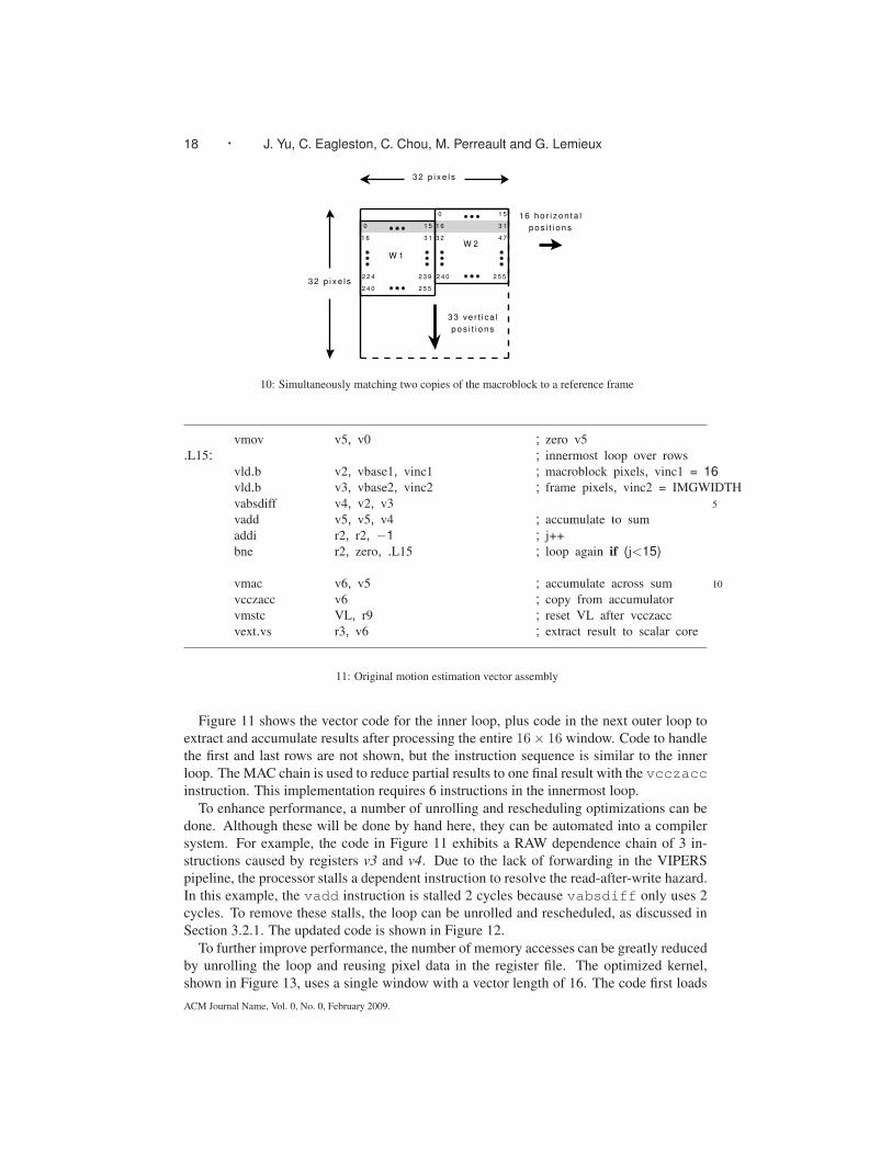
the current macroblock can be matched against the search area simultaneously. Figure 10
shows how this is accomplished using only unit stride load memory instructions, which
execute the fastest, in the inner loop. The two copies of the macroblock are offset vertically
by one row. For each position within the search range, 17 rows are processed, with the
calculations in the first and last row partially masked using a vector flag register.
ACM Journal Name, Vol. 0, No. 0, February 2009.
18 · J. Yu, C. Eagleston, C. Chou, M. Perreault and G. Lemieux
0 1 5
0 1 5
1 6 3 1
1 6 3 1 3 2 4 7
2 4 0 2 5 5
2 4 0 2 5 5
2 2 4 2 3 9
W 1
W 2
3 2 p i x e l s
3 2 p i x e l s
33 ve r t i ca l
p o s i t i o n s
1 6 h o r i z o n t a l
p o s i t i o n s
10: Simultaneously matching two copies of the macroblock to a reference frame
vmov v5, v0 ; zero v5
.L15: ; innermost loop over rows
vld.b v2, vbase1, vinc1 ; macroblock pixels, vinc1 = 16
vld.b v3, vbase2, vinc2 ; frame pixels, vinc2 = IMGWIDTH
vabsdiff v4, v2, v3 5
vadd v5, v5, v4 ; accumulate to sum
addi r2, r2, −1 ; j++
bne r2, zero, .L15 ; loop again if (j<15)
vmac v6, v5 ; accumulate across sum 10
vcczacc v6 ; copy from accumulator
vmstc VL, r9 ; reset VL after vcczacc
vext.vs r3, v6 ; extract result to scalar core
11: Original motion estimation vector assembly
Figure 11 shows the vector code for the inner loop, plus code in the next outer loop to
extract and accumulate results after processing the entire 16× 16 window. Code to handle
the first and last rows are not shown, but the instruction sequence is similar to the inner
loop. The MAC chain is used to reduce partial results to one final result with the vcczacc
instruction. This implementation requires 6 instructions in the innermost loop.
To enhance performance, a number of unrolling and rescheduling optimizations can be
done. Although these will be done by hand here, they can be automated into a compiler
system. For example, the code in Figure 11 exhibits a RAW dependence chain of 3 in-
structions caused by registers v3 and v4. Due to the lack of forwarding in the VIPERS
pipeline, the processor stalls a dependent instruction to resolve the read-after-write hazard.
In this example, the vadd instruction is stalled 2 cycles because vabsdiff only uses 2
cycles. To remove these stalls, the loop can be unrolled and rescheduled, as discussed in
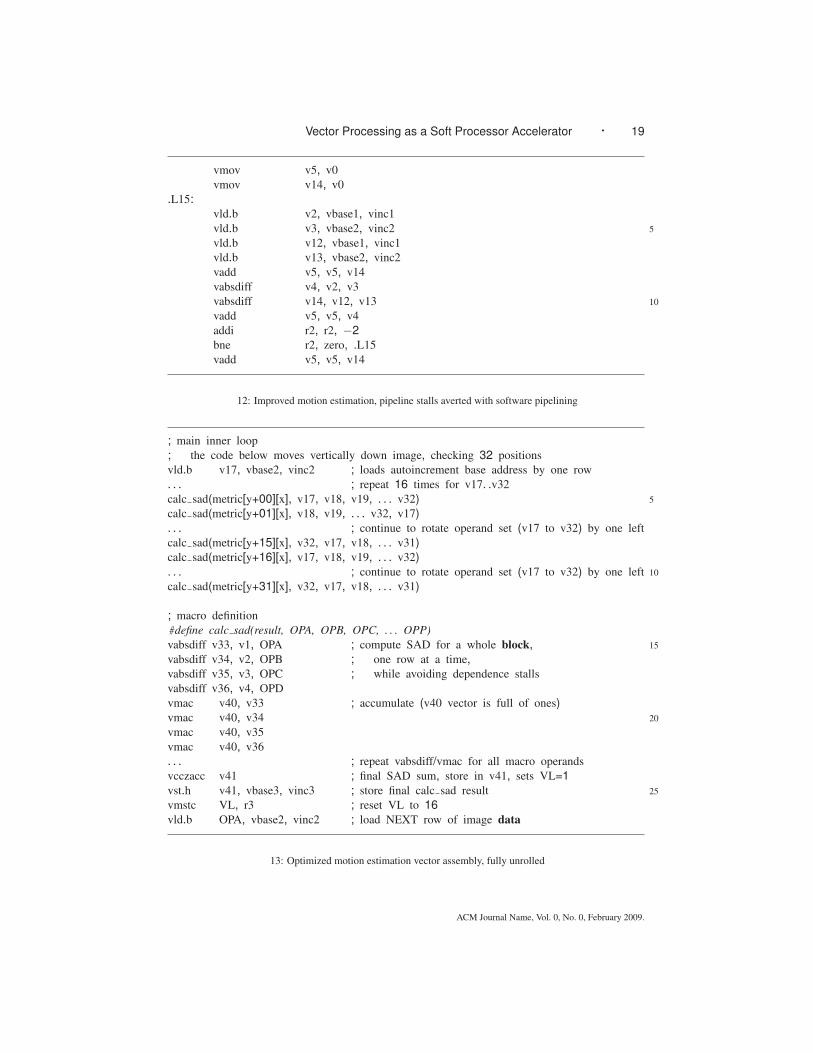
Section 3.2.1. The updated code is shown in Figure 12.
To further improve performance, the number of memory accesses can be greatly reduced
by unrolling the loop and reusing pixel data in the register file. The optimized kernel,
shown in Figure 13, uses a single window with a vector length of 16. The code first loads
ACM Journal Name, Vol. 0, No. 0, February 2009.
Vector Processing as a Soft Processor Accelerator · 19
vmov v5, v0
vmov v14, v0
.L15:
vld.b v2, vbase1, vinc1
vld.b v3, vbase2, vinc2 5
vld.b v12, vbase1, vinc1
vld.b v13, vbase2, vinc2
vadd v5, v5, v14
vabsdiff v4, v2, v3
vabsdiff v14, v12, v13 10
vadd v5, v5, v4
addi r2, r2, −2
bne r2, zero, .L15
vadd v5, v5, v14
12: Improved motion estimation, pipeline stalls averted with software pipelining
; main inner loop
; the code below moves vertically down image, checking 32 positions
vld.b v17, vbase2, vinc2 ; loads autoincrement base address by one row
. . . ; repeat 16 times for v17. .v32
calc sad(metric[y+00][x], v17, v18, v19, . . . v32) 5
calc sad(metric[y+01][x], v18, v19, . . . v32, v17)
. . . ; continue to rotate operand set (v17 to v32) by one left
calc sad(metric[y+15][x], v32, v17, v18, . . . v31)
calc sad(metric[y+16][x], v17, v18, v19, . . . v32)
. . . ; continue to rotate operand set (v17 to v32) by one left 10
calc sad(metric[y+31][x], v32, v17, v18, . . . v31)
; macro definition
#define calc sad(result, OPA, OPB, OPC, . . . OPP)
vabsdiff v33, v1, OPA ; compute SAD for a whole block, 15
vabsdiff v34, v2, OPB ; one row at a time,
vabsdiff v35, v3, OPC ; while avoiding dependence stalls
vabsdiff v36, v4, OPD
vmac v40, v33 ; accumulate (v40 vector is full of ones)
vmac v40, v34 20
vmac v40, v35
vmac v40, v36
. . . ; repeat vabsdiff/vmac for all macro operands
vcczacc v41 ; final SAD sum, store in v41, sets VL=1
vst.h v41, vbase3, vinc3 ; store final calc sad result 25
vmstc VL, r3 ; reset VL to 16
vld.b OPA, vbase2, vinc2 ; load NEXT row of image data
13: Optimized motion estimation vector assembly, fully unrolled
ACM Journal Name, Vol. 0, No. 0, February 2009.

20 · J. Yu, C. Eagleston, C. Chou, M. Perreault and G. Lemieux
for( i=0; i<12; i++ ) { // sort top half of array
min = array[i];
for( j=i+1; j<=24; j++ )
if( array[j] < min ) swap min, array[j];
array[i]=min; 5
}min = array[12];
for( j=13; j<=24; j++ ) // last pass, find median
if( array[j] < min ) min = array[j];
return min; 10
14: 5 × 5 median filter C code
S l i d i n g w i n d o w
O u t p u t p i x e l
15: Vectorizing the image median filter
all 16 rows of the reference frame into vector registers. Note how the calc sad() macro
avoids dependence stalls by grouping sets of four independent instructions together. When
shifting the block vertically one position, it reuses 15 of the 16 rows of pixels from the
reference frame. An updated SAD value for the new position is then calculated. This
unrolled approach is up to five times faster, but it requires significantly more instruction
memory and vector registers.
4.2 Image Median Filter
The median filter replaces each pixel with the median value of a surrounding 5×5 window.
Figure 14 presents C code that performs a bubble sort on a 5 × 5 image region, stopping
early after the top half is sorted to locate the median.
The median filter kernel vectorizes nicely by exploiting outer-loop parallelism. Fig-
ure 15 shows how this can be done. Each strip represents one row of MVL pixels, and each
row is loaded into a separate vector register. The window of pixels that is being processed
will then reside in the same data element over 25 vector registers. After initial setup, the
same filtering algorithm as the scalar code can then be used. Figure 16 shows the inner
loop vector assembly. This implementation generates MVL results at a time. Thus, an
8-lane vector processor will generate 32 results at once.
To further improve performance, the median filter kernel was fully unrolled as shown
ACM Journal Name, Vol. 0, No. 0, February 2009.

Vector Processing as a Soft Processor Accelerator · 21
.L14:
vld.b v2, vbase2, vinc0 ; vector load array[j]
vmax v31, v2, v4 ; remember bignum in v31
vmin v4, v2, v4 ; remember minnum in v4
vst.b v31, vbase2, vinc1 ; store bignum to array[j] 5
addi r2, r2, 1
bge r6, r2, .L14
vst.b v4, vbase1, vinc1 ; store minnum to array[i]
16: Median filter inner loop vector assembly
; load one vector register, repeat 25 times for v1. .v25
vld.b v1, vbase1, vinc1 ; load row of image, vinc1=VL
; make a comparison between two rows of pixels and swap
; repeat 222 times for v i,v j (for all i=1. .12, j=i+1. .25) 5
vmax v31, v1, v2
vmin v1, v1, v2
vmov v2, v31
; last pass, find the min, repeat 12 times for v14. .v25 10
vmin v13, v13, v14
vst.b v13, vbase2, vinc1 ; save median values
17: Optimized median filter vector assembly, fully unrolled
in Figure 17. All 25 vector registers are loaded at the beginning to eliminate subsequent
vector loads. All vector stores are eliminated except one at the very end. By eliminating
the redundant loads and stores, this unrolled approach is about three times faster. However,
it also requires significantly more instruction memory.
4.3 AES Encryption
The AES encryption kernel computes 10 rounds of encryption on 128 bits of data using
a 128-bit key. Only performance results for one intermediate round are included in the
kernel, as the final round is slightly different and is not within the main loop.
The AES encryption algorithm [National Institute of Standards and Technology 2001]
used here is taken from the MiBench suite [Guthaus et al. 2001]. Each block of 128 bits
can be arranged into a 4 × 4 matrix of bytes, termed the AES state. The implementation
uses a 1KB (256x32b) lookup-table described in [Daemen and Rijmen 2002].
The AES encryption kernel can exploit outer-loop parallelism by loading multiple blocks
to be encrypted into different vector lanes. Each 32-bit column of the 128-bit AES state
fits into one element of a vector register when VPUW = 32. A vector processor with MVL
of 32 can encrypt 32 blocks (4096 bits) of data at a time.
The vector assembly code to encrypt one of the four columns, forming just part of a
single round transformation, is shown in Figure 18. Code to initialize the lookup tables is
ACM Journal Name, Vol. 0, No. 0, February 2009.

22 · J. Yu, C. Eagleston, C. Chou, M. Perreault and G. Lemieux
; Load Plaintext
vlds.w v1, vbase0, vstride4, vinc1 ; Load 4 columns of plaintext
vlds.w v2, vbase0, vstride4, vinc1 ; (stride 4, one AES column)
vlds.w v3, vbase0, vstride4, vinc1 ;
vlds.w v4, vbase0, vstride4, vinc1 ; 5
; Initialization
vxor.vs v1, v1, r2 ; Initialize with keys
vxor.vs v2, v2, r3 ; (keys preloaded in r2. .r5)
vxor.vs v3, v3, r4 ; 10
vxor.vs v4, v4, r5 ;
; Do 10 rounds * 4 columns
; Round 1 column 1 (r1c1) shown below; last round is slightly different
ldw r2, 0(r6) ; r1c1 load next key 15
vsrl v9, v4, v11 ; r1c1 shift right 24 bits
vldl v9, v9 ; r1c1 S−box table lookup
vrot v9, v9, v11 ; r1c1 mixcolumns
vxor.vs v5, v9, r2 ; r1c1 add new round key
20
vsrl v9, v3, v12 ; r1c1 shift right 16 bits
vldl v9, v9 ; r1c1 S−box table lookup
vrot v9, v9, v12 ; r1c1 rotation 16 bits
vxor v5, v5, v9 ; r1c1 mixcolumns
25
vsrl v9, v2, v13 ; r1c1 shift right 8 bits
vldl v9, v9 ; r1c1 S−box table lookup
vrot v9, v9, v13 ; r1c1 rotation 8 bits
vxor v5, v5, v9 ; r1c1 mixcolumns
30
vldl v9, v1 ; r1c1 S−box table lookup
vxor v5, v5, v9 ; r1c1 mixcolumns
; repeat for r1c2, r1c3, r1c4, r2c1, r2c2, etc
18: Vector assembly for loading AES state and part of one AES encryption round
not shown. The plaintext AES state is loaded from memory into vector registers v1 to v4
using four stride-four load word instructions. Each AES block now resides within a single
vector lane, across these four vector registers. For each round transformation requires
executing 60 vector and 7 scalar instructions.
4.4 Benchmark Tuning for C2H Compiler
The C2H compiler generates a single hardware accelerator for a given C function. The
first set of accelerators, termed “push-button”, is generated by compiling the source with
as little modification as possible.
Additional accelerators are generated by modifying the C code to vary the perfor-
mance/resource tradeoff. Manual transformations are necessary because C2H does not
provide the ability to control the amount of loop unrolling or set performance/resource
ACM Journal Name, Vol. 0, No. 0, February 2009.
Vector Processing as a Soft Processor Accelerator · 23
goals. Selecting and unrolling loops involves applying similar concepts to those learned
from vectorizing the benchmark. It also requires additional temporary variables (registers)
to calculate multiple results in parallel. Hardware knowledge is needed to understand how
this creates additional parallelism through pipelining and spatial replication.
Manual unrolling is error-prone, and the resulting C code is ugly and cumbersome to
modify. Although unrolling the vector assembly code in this paper is also done manually,
we found unrolled C2H code more difficult to manage. In particular, the AES code, which
is more complex than the other benchmarks, was the most challenging to modify. To
improve performance, each of the four table-lookup operations needs a dedicated 256-
entry, 32-bit memory. Local tables can be automatically created by the compiler, but these
must be global to facilitate initialization. Hence, they were manually added to the Nios II
memory system. The AES engine was then replicated to support multiple streams, but all
streams share the same four lookup tables.
5. AREA AND PERFORMANCE RESULTS
This section compares area and speedup results for the three benchmark applications be-
tween the Nios II soft processor, the VIPERS soft vector processor, and the Altera C2H
compiler.
5.1 Resource Utilization
Performance and area scalability was one of the primary design goals of VIPERS. This
section gives VIPERS area utilization and clock frequency trends for different combina-
tions of configuration parameters, and compares resource usage of VIPERS to Nios II and
C2H accelerators. All compilation is performed using Altera’s Quartus II version 7.2.
5.1.1 VIPERS Resource Utilization. To illustrate the scalability of VIPERS, several
configurations with different parameter settings are shown in Tables III and IV.
Table III illustrates the range in resource utilization when changing NLane from 16 down
to 4. The VxF configurations consist of x vector lanes, the full feature set of the architec-
ture, and support 8-, 16-, and 32-bit data access granularity. The flexible memory interface
is the single largest individual component of the processor. It uses over 50% of the ALMs
in V4F, and 35% of the ALMs in V16F. Setting MemMinWidth to 16 and 32, indicated
by y in VxMy, changes the minimum data access granularity. This affects the size of the
memory crossbars; a larger value saves more area.
Table IV shows the effect of successively removing secondary processor features from a
V8F configuration. The V8Cz configurations remove local memory, distributed accumula-
tors and vector lane multipliers, and vector insert/extract and element shifting instructions,
respectively. Area can be further reduced by adjusting the primary parameters: V8W16 re-
duces VPUW to 16, and V8W16M16 supports only 16-bit memory accesses. Overall, more
than 3,700 ALMs can be saved if these features are not needed. This savings is enough to
implement six additional Nios II/s processor cores.
These results demonstrate that resource usage can span a wide range, depending upon
the performance and processor features needed. Some additional savings may be possible
by fine-grained instruction subsetting, but VIPERS does not currently support this feature.
5.1.2 Resource Comparison to Nios II and C2H. Application-specific configurations
of the soft vector processor, C2H accelerators, and the Nios II/s processor were compiled
to measure their resource usage. The Nios II/s (standard) version is used as the baseline for
ACM Journal Name, Vol. 0, No. 0, February 2009.

24 · J. Yu, C. Eagleston, C. Chou, M. Perreault and G. Lemieux
Table III. VIPERS resource usage from varying NLane and MemMinWidth
Vector Processor Configuration (UT IIe+)
Resource V16F V16M16 V16M32 V4F V4M16 V4M32
ALM 10,995 9,149 8,163 5,825 4,278 3,414
DSP Elements 86 82 82 25 21 21
M9K 56 57 54 21 21 20
Fmax (MHz) 105 110 107 106 113 116
Parameter Values
NLane 16 16 16 4 4 4
MemMinWidth 8 16 32 8 16 32
Table IV. VIPERS resource usage from varying secondary processor parameters
Vector Processor Configuration (UT IIe+)
Resource V8F V8C1 V8C2 V8C3 V8W16 V8W16M16
ALM 7,501 7,505 6,911 6,688 5,376 3,790
DSP Elements 46 46 6 6 6 2
M9K 33 25 25 25 25 24
Fmax (MHz) 110 105 107 113 114 121
Parameter Values
NLane 8 8 8 8 8 8
MVL 32 32 32 32 32 32
VPUW 32 32 32 32 16 16
MemWidth 128 128 128 128 128 128
MemMinWidth 8 8 8 8 8 16
MACL 2 2 0 0 0 0
LMemN 256 0 0 0 0 0
LMemShare On Off Off Off Off Off
Vmult On On Off Off Off Off
Vmanip On On On Off Off Off
Vupshift On On On Off Off Off
Table V. Resource usage of VIPERS and C2H configurations
Stratix III (C3) ALM DSP Elements M9K MHz
Biggest -340 device 135,000 576 1,040 –
Smallest -50 device 19,000 216 108 –
General-purpose configurations
Nios II/s 537 4 6 203
UT IIe 376 0 3 170
UT IIe+V16F 10,955 86 56 105
Benchmark-specific VIPERS configurations
UT IIe+V16 Median 7,330 38 41 111
UT IIe+V16 Motion 7,983 54 41 105
UT IIe+V16 AES 7,381 66 56 113
Stratix II (C3) ALM DSP Elements M4K MHz
Benchmark-specific accelerators
Nios II/s+C2H Median 825 8 4 147
Nios II/s+C2H Motion 972 10 4 121
Nios II/s+C2H AES 2,480 8 6 119
ACM Journal Name, Vol. 0, No. 0, February 2009.

Vector Processing as a Soft Processor Accelerator · 25
Table VI. VIPERS performance model
Instruction Class Instruction Cycles Example Value∗
Scalar other 4 4Scalar store 5 5Scalar load 6 6Vector-scalar ⌈V L/NLane⌉+2 6Vector-vector ⌈V L/NLane⌉ 4Vector local memory ⌈V L/NLane⌉ 4Vector load C + ⌈StrideLength/NumElem1⌉† + ⌈V L/NLane⌉ 24 or 40Vector store C + ⌈StrideLength/NumElem2⌉† + ⌈V L/NLane⌉ 24 or 40Indexed load/store C + V L‡ + ⌈V L/NLane⌉ 72
MaxElem = MemWidth/V ecDataWidth 4NumElem1 = min(NLane, MaxElem) 4NumElem2 = min(NLane, MaxElem, MemWidth/V PUW ) 4StrideLength = V L ·min(Stride, NumElem1) 128V ecDataWidth is the data width of the particular vector memory access 32C is 4 for vector loads or stores; add 1 extra cycle for unaligned addresses 4∗assumes NLane = 16, V PUW = 32, MemWidth = 128, V L = 64, Stride = 1 or 2†this portion of latency can be hidden by overlapping execution with non-memory instructions‡overlapped execution for this portion of latency is possible, but not yet implemented
area comparisons. The Nios II/s comes with a 5-stage pipeline, static branch prediction,
and a 3-cycle multiplier and shifter. It is further configured with a 1 KB instruction cache,
32 KB each of on-chip program and data memory, and no debug core. Compilation targets
a Stratix III EP3SL340 device in the C3 speed grade.1
Table V summarizes the resource usage of various system configurations. The V16 Me-
dian, V16 Motion, and V16 AES labels denote application-specific minimal configurations
of VIPERS with 16 lanes used for performance benchmarking. Median filtering and mo-
tion estimation do not require any 32-bit vector processing, so 16-bit ALUs are used. No
local memories are instantiated for these two benchmarks, and MAC units were instan-
tiated only for motion estimation. The AES encryption kernel requires only 32-bit word
access, so MemMinWidth was set to 32 bits. The AES kernel also requires a 256-word
vector lane local memory. These customizations save about 30% of ALMs required by a
full 16-lane processor.
5.2 Performance Results
This section compares the performance of VIPERS to the Nios II processor and C2H ac-
celerators. In addition, performance of VIPERS is compared to a hand-crafted RTL imple-
mentation.
5.2.1 Performance Models and Methodology. Performance of Nios II, VIPERS, and
C2H accelerators are compared using execution time of the three benchmark kernels. Ex-
ecution time is the product of total clock cycles and the minimum clock period (1/Fmax).
The three target architectures use three different methods for calculating the total clock
cycles; these will be described shortly. The Altera Quartus II TimeQuest analyzer is used
to determine Fmax.
The Nios II processor cycles form the baseline case for all speedups. They are deter-
1The C2H compiler does not yet support Stratix III, so it targets a Stratix II device in the C3 speed grade. The
architectures have similar ALMs, but different memory and DSP blocks.
ACM Journal Name, Vol. 0, No. 0, February 2009.
26 · J. Yu, C. Eagleston, C. Chou, M. Perreault and G. Lemieux
mined by assuming an ideal pipelined processor. In this model, every Nios II instruction is
executed in 1 clock cycle, including memory operations and branches; there are no stalls,
mispredictions, cache misses, etc. This gives the best-possible Nios II performance. For
area and Fmax results, a real Nios II/s processor is used.
The number of cycles required by each C2H accelerator is extracted from the C2H com-
piler performance report. Cycles are calculated for the main loop only, using the loop
latency and cycles per loop iteration figures. Only the accelerator performance is consid-
ered; no Nios II instructions are included. It is worth noting that this measure of C2H
performance is optimistic because usually Nios II caches must be flushed prior to invoking
the accelerator. For area and Fmax results, the accelerators are compiled targeting a slower
Stratix II architecture.
The VIPERS processor cycles are determined by running the benchmark inside the Mod-
elSim Verilog simulator and counting the cycles. This produces a realistic, cycle-accurate
result of the RTL implementation. This captures all pipeline and memory stalls as well
as concurrent operation of vector memory, vector arithmetic, and scalar instructions. It is
worth noting that the UT IIe scalar core used in VIPERS requires four cycles to execute
each scalar instruction. This adds considerable overhead to the median filter benchmark,
for example. For area and Fmax results, application-specific instances of VIPERS are used.
To help software programmers optimize their code, the performance model in Table VI
summarizes the cycles to execute several types of instructions. These values are deter-
mined from our knowledge of the Verilog source and ModelSim simulation experience.
Most scalar instructions take four cycles each, except memory operations which take longer
because of the memory crossbars. Vector instructions vary depending upon run-time con-
ditions, but typical cases require 4 cycles to execute a vector length of 64 across 16 lanes.
Vector loads and stores, however, need additional cycles due to load buffers, store buffers,
strided access, and data alignment. Hence, the performance model gives the execution la-
tency for several different situations. Each equation typically has three terms: a constant
term for instruction issue and other overhead, a variable term for data transfer between the
vector register file and the load/store buffer, and another variable term for data transfer and
re-alignment through the crossbars between the load/store buffer and memory.
Due to stalls, concurrency, changes to the vector length, and other dynamic runtime
situations, VIPERS instructions do not always take the same number of cycles to execute.
The performance model in Table VI does not capture these dynamic events. For example,
it ignores dependence stalls and the potential overlap of scalar, vector, and vector memory
instructions. In particular, in some situations a significant part of the load or store latency
can be hidden by the load/store buffers. Programmers will have to use their experience and
intuition to determine the impact of these types of events when optimizing their code.
5.2.2 Vector and C2H Performance Comparison. Table VII shows the performance
of Nios II, C2H, and several VIPERS configurations on the three benchmarks. The C2H
results are from the “push-button” compilation.
Despite having a lower clock frequency, all vector configurations show speedup over the
baseline Ideal Nios II/s. Some of the improvement comes from lower loop overhead, as
vector instructions significantly reduce the number of increment/compare/branch instruc-
tions executed. In addition, greater performance is obtained when more vector lanes are
used. The instruction count and clock cycles per result decreases for median filtering and
AES encryption as more vector lanes are added because more results are computed in par-
ACM Journal Name, Vol. 0, No. 0, February 2009.

Vector Processing as a Soft Processor Accelerator · 27
Table VII. Performance results
Ideal VIPERS
Nios II/s C2H V4 V8 V16
Fmax (MHz) determined using: Stratix III Stratix II Stratix III
Median Filtering 203 147 117 108 111Motion Estimation 203 121 119 108 105AES Encryption Rnd. 203 119 130 120 113
Dynamic Instruction Count
Median Filtering (per pixel) 2,164 93 47 23Motion Est. (entire search range) 2,612,416 111,840 56,232 56,232AES Encryption Rnd. (per 128b blk) 94 4.2 2.1 1.1Median Filtering, fully unrolled 44 22 11Motion Est., fully unrolled 37,568 37,568 37,568
Clock Cycles determined using: instr. count C2H report execution under ModelSim
Median Filtering (per pixel) 2,164 1,848 496 256 141Motion Est. (entire search range) 2,612,416 694,468 717,120 346,203 269,214AES Encryption Rnd. (per 128b blk) 94 25 16 8 4Median Filtering, fully unrolled 189 95 48Motion Est., fully unrolled 157,792 88,288 55,328
Speedup
Median Filtering (per pixel) 1.0 0.8 2.5 4.5 8.4Motion Est. (entire search range) 1.0 2.1 2.1 4.0 5.0AES Encryption Rnd. (per 128b blk) 1.0 2.2 3.9 7.2 13.5Median Filtering, fully unrolled 6.6 12.1 24.9Motion Est., fully unrolled 9.7 15.7 24.4
allel. Note this sometimes results in fractional instruction counts per block after the total
instructions are divided by the number of blocks encrypted in parallel.
For the motion estimation kernel (not unrolled), two versions of the code are used: one
for V4 with a vector length of 16, and another for V8 and V16 with a vector length of 32. In
the second version, the assembly source handles two SAD window calculations in parallel
using the code shown in Figure 12. The fully unrolled motion estimation is a third version
of the code where all processor configurations run the same single-window code using a
vector length of 16.
Figure 19 plots speedup of the VIPERS processors and C2H accelerators in comparison
to the execution time of the ideal Nios II single-cycle model. This is plotted against the
number of ALMs used, normalized to the real Nios II/s core. The bold/dark lines show
performance of VIPERS with 4, 8, and 16 vector lanes. The median filtering and AES
results also include a 32-lane version. The filled/gray data points show performance of the
“push-button” C2H accelerators, and the thin/gray lines show the performance improve-
ment when the C2H accelerators are scaled and optimized as described in Section 4.4.
Note the diagonal line shows one-to-one speedup versus area, representing speedup of a
MIMD multiprocessor system that has no interconnect or communication overhead.
The 4-lane VIPERS configurations for all three benchmarks have a 64-bit memory in-
terface, while configurations with more lanes have a 128-bit memory interface. The 64-bit
interface requires fewer ALMs, pushing the V4 points farther left (lower area) in the graph.
This often produces in a visual “kink” at the V8 configuration. This is not as apparent in
the V8 configuration for AES, which has a smaller memory interface due to support for
only 32-bit words, or motion estimation where a different (slower) version of the code is
used. This illustrates the large overhead of the vector memory interface. When the number
of vector lanes increases to 16, AES quickly catches up in ALM usage because it uses
VPUW = 32 instead of VPUW = 16 for the others.
Speedups of the “push-button” C2H accelerators are similar to those of the V4 proces-
ACM Journal Name, Vol. 0, No. 0, February 2009.

28 · J. Yu, C. Eagleston, C. Chou, M. Perreault and G. Lemieux
1 5 10 20 30 40 50
1
5
10
20
30
40
50
Normalized Resource (ALM/ALM)
Speedup
Motion Est. Vector Opt
Median Filter Vector Opt
AES Vector
Motion Est. Vector
Median Filter Vector
Motion Est. C2H
AES C2H
Median Filter C2H
19: Vector and C2H speedup versus area, normalized to Nios II
sor configurations for motion estimation and AES. For the median filter, however, C2H is
slower than Nios II, partly due to a drop in clock speed.2 Although performance increases
by scaling the C2H accelerators, notice that it saturates in all cases. After being unrolled
many times, simultaneous access to the same variables in main memory eventually be-
comes the bottleneck. Adding the four lookup tables for the AES kernel achieves a large
speedup over the “push-button” result, indicated by the large jump of the second data point
on the curve. Further replicating the AES engine up to four times creates contention at
these lookup table memories and results in little additional speedup. In all three bench-
marks, additional C2H performance is possible by manually changing the Nios II memory
system.
In contrast, a soft vector processor automatically scales performance by scaling the num-
ber of vector lanes. This scales the vector register file bandwidth at the same time. Since
most operations inside inner loops of kernels read and write vector registers, increasing the
register file bandwidth allows more data elements to be accessed and processed in paral-
lel each cycle, increasing performance. This avoids the need to re-architect the memory
system as required with C2H. The vector programming model is a powerful abstraction
for this scalable architecture, providing the same unified memory system to the user across
several different configurations with zero hardware design effort.
5.2.3 Vector and RTL Performance Comparison. Motion estimation and AES are
commonly implemented using hand-crafted RTL accelerators. In particular, changes to the
motion estimation algorithm are common, so a flexible software implementation would
be more desirable than a fixed hardware implementation. Hence, it is useful to compare
performance of VIPERS to an fixed RTL implementation.
Motion estimation in VIPERS with 16 lanes achieves a throughput of 1,898 full block
2In our earlier work [Yu et al. 2008; Yu 2008], we forgot to turn on the C optimizer for the Nios II median filter
results. Hence, the C2H and VIPERS speedups are lower here.
ACM Journal Name, Vol. 0, No. 0, February 2009.

Vector Processing as a Soft Processor Accelerator · 29
searches per second (FBSS). In comparison, a fixed FPGA-based RTL implementation de-
scribed in [Li and Leong 2008] achieves 155,239 FBSS, which is 82× faster. However, one
small change to the VIPERS ISA (combining vabsdiff and vmac into one instruction)
can nearly double its throughput. Also, a higher clock frequency with deeper pipelining
can potentially double it again. These two improvements would shorten the RTL advantage
to just 21× faster. Although it is not as fast as hardware, it is impressive to achieve this
speed with a purely software approach.
The VIPERS and hand-crafted RTL approaches are similar in area. The hand-crafted
RTL uses 5,789 Xilinx Virtex-II Pro slices, compared to 7,983 ALMs for VIPERS.3
5.2.4 Vector Software Optimization. The aggressive unrolling of the median filter and
motion estimation benchmarks, shown as the dotted lines in Figure 19, produce significant
performance improvements. In both cases, the main idea is to re-use data in the vec-
tor registers as much as possible to avoid redundant memory loads. Also, loop overhead
instructions are eliminated. This produces an impressive 3 to 5 times speedup over the
original vector code, and shows how important it is to pay attention to memory operations.
In the vector programming model, costly vector load and store operations are explicit. This
gives programmers an explicit target to optimize.
Programming in vector assembly and achieving this level of performance is not difficult.
In three weeks, a 3rd year ECE undergraduate was able to study the VIPERS documentation
and speed up both applications. The student had taken introductory courses in digital logic
and assembly language programming, but had no background in computer architecture or
VHDL/Verilog design.
6. CONCLUSIONS AND FUTURE WORK
As the performance requirements and complexity of embedded systems continue to in-
crease, designers need a high performance platform that reduces development effort and
time-to-market. A soft vector processor provides the advantages of scalable performance
and resource usage, being simple to use with no hardware design knowledge or effort, and
early decoupling of the hardware (RTL) and software design flows. Decoupling the flows
is extremely important because software changes will not introduce additional hardware
recompiles, saving many lengthy place-and-route iterations and more quickly reaching
timing closure for the entire system. It also means a single vector processor can serve as a
general-purpose accelerator for multiple applications.
Embedded software programmers can easily understand and control performance and
area through a configurable number of vector lanes and the vector ALU width. Also,
programmers can easily optimize software performance by applying the vector memory
model; reusing data in vector registers is highly preferred to re-reading data from memory.
The soft vector processor architecture developed in this paper, VIPERS, outperforms
a Nios II processor and the Altera C2H compiler on the three benchmarks shown. For
example, VIPERS with 16 vector lanes achieves a speedup of 25× with just 14× the area
of a Nios II processor on the median filter. The VIPERS implementation includes a flexible,
single-bank memory interface that can support different memory widths and data access
granularities of 8, 16, or 32 bits. This vector memory interface is a significant fraction of
the total area, and also contains the critical path of the system. By customizing the soft
3Each slice contains two 4-input LUTs; each ALM is a 6-input LUT.
ACM Journal Name, Vol. 0, No. 0, February 2009.

30 · J. Yu, C. Eagleston, C. Chou, M. Perreault and G. Lemieux
vector processor to the benchmarks, area savings of 30% was achieved compared to a full-
featured configuration with 16 lanes. This 30% is a large amount of silicon—enough logic
to implement six more Nios II/s processors.
Performance of the current implementation is hindered by a slow scalar core. The ability
to overlap execution of scalar instructions via traditional pipelining is a minimum first step.
However, increased overlap of scalar and vector instructions is also needed through a dual-
issue approach. The best way to implement this needs to be studied.
Future work should also consider architectural improvements to the vector core. One
benefit of working with a soft vector architecture is that architectural proposals do not have
to benefit all applications. This is because features can be selectively included at system
generation time. For example, a new vfir instruction that uses the FIR mode of the
DSP blocks would be useful for only some applications. Another benefit of working with
FPGA-based implementations is the cost of resources is very different than a full-custom
approach. For example, the hardware multipliers are already built into FPGA devices; full-
custom vector processors must consider the tradeoff whether to build a multiplier or more
on-chip memory, but FPGA implementations can use a multiplier for free. This new cost
framework makes it important to re-evaluate past architectural ideas in addition to more
recent ones such as CODE [Kozyrakis and Patterson 2003b] and the vector-thread (VT)
architecture [Krashinsky et al. 2004].
ACKNOWLEDGMENTS
The authors would like to thank Blair Fort for providing the UT IIe processor for this re-
search. We also thank the anonymous referees for their helpful suggestions. This research
was supported by NSERC and Altera.
REFERENCES
ALTERA CORP. 2008a. Avalon Interface Specifications, 1.0 ed.
ALTERA CORP. 2008b. Nios II C2H Compiler User Guide, 8.0 ed.
ALTERA CORP. 2008c. Nios II Processor Reference Handbook, 8.0 ed.
ARC INTERNATIONAL. 2008. Configurable CPU/DSP processors. http://www.arc.com/configurablecores/index.html.
ASANOVIC, K. 1998. Vector microprocessors. Ph.D. thesis, EECS Dept., University of California, Berkeley.
BROST, V., YANG, F., AND PAINDAVOINE, M. 2007. A modular VLIW processor. In IEEE Int. Symp. on
Circuits and Systems. 3968–3971.
CASPER, J., KRASHINSKY, R., BATTEN, C., AND ASANOVIC, K. 2005. A parameterizable FPGA prototype of
a vector-thread processor. Workshop on Architecture Research using FPGA Platforms, as part of HPCA-11.
CHEN, S., VENKATESAN, R., AND GILLARD, P. 2008. Implementation of vector floating-point processing
unit on FPGAs for high performance computing. In IEEE Canadian Conf. on Elec. and Comp. Engineering.
881–885.
CHO, J., CHANG, H., AND SUNG, W. 2006. An FPGA-based SIMD processor with a vector memory unit. In
Int. Symp. on Circuits and Systems. 525–528.
DAEMEN, J. AND RIJMEN, V. 2002. The design of Rijndael: AES — the Advanced Encryption Standard. Spring-
er-Verlag.
DIEFENDORFF, K., DUBEY, P. K., HOCHSPRUNG, R., AND SCALE, H. 2000. AltiVec extension to PowerPC
accelerates media processing. IEEE Micro 20, 2 (Mar./Apr.), 85–95.
DINH, Q., CHEN, D., AND WONG, D. 2008. Efficient ASIP design for configurable processors with fine-grained
resource sharing. In ACM/SIGDA Int. Symp. on FPGAs.
EDWARDS, S. A. 2006. The challenges of synthesizing hardware from C-like languages. IEEE Design & Test
of Computers 23, 5 (May), 375–386.
EEMBC. 2008. The embedded microprocessor benchmark consortium. http://www.eembc.org/.
ACM Journal Name, Vol. 0, No. 0, February 2009.

Vector Processing as a Soft Processor Accelerator · 31
FORT, B., CAPALIJA, D., VRANESIC, Z. G., AND BROWN, S. D. 2006. A multithreaded soft processor for
SoPC area reduction. In IEEE Symp. on Field-Programmable Custom Computing Machines. 131–142.
GRABBE, C., BEDNARA, M., VON ZUR GATHEN, SHOKROLLAHI, J., AND TEICH, J. 2003. A high perfor-
mance VLIW processor for finite field arithmetic. In Int. Parallel and Distributed Processing Symp. 189b.
GUTHAUS, M., RINGENBERG, J., ERNST, D., AUSTIN, T., MUDGE, T., AND BROWN, R. 2001. MiBench: a
free, commercially representative embedded benchmark suite. In IEEE Int. Workshop on Workload Charac-
terization. 3–14.
HABATA, S., YOKOKAWA, M., AND KITAWAKI, S. 2003. The Earth simulator system. NEC Research &
Development Journal 44, 1 (Jan.), 21–16.
HASAN, M. Z. AND ZIAVRAS, S. G. 2005. FPGA-based vector processing for solving sparse sets of equations.
In IEEE Symp. on Field-Programmable Custom Computing Machines. 331–332.
HWANG, K. AND BRIGGS, F. A. 1984. Computer Architecture And Parallel Processing. McGraw-Hill Inc.
JACOB, A. C., HARRIS, B., BUHLER, J., CHAMBERLAIN, R., AND CHO, Y. H. 2006. Scalable softcore vector
processor for biosequence applications. In IEEE Symp. on Field-Programmable Custom Computing Machines.
JONES, A. K., HOARE, R., KUSIC, D., FAZEKAS, J., AND FOSTER, J. 2005. An FPGA-based VLIW processor
with custom hardware execution. In ACM/SIGDA Int. Symp. on Field Programmable Gate Arrays. 107–117.
KOZYRAKIS, C. AND PATTERSON, D. 2003a. Overcoming the limitations of conventional vector processors.
In Int. Symp. on Computer Architecture. 399–409.
KOZYRAKIS, C. AND PATTERSON, D. 2003b. Scalable, vector processors for embedded systems. IEEE Mi-
cro 23, 6 (Nov./Dec.), 36–45.
KRASHINSKY, R., BATTEN, C., HAMPTON, M., GERDING, S., PHARRIS, B., CASPER, J., AND ASANOVIC,
K. 2004. The vector-thread architecture. In Int. Symp. on Computer Architecture. 52–63.
LI, B. AND LEONG, P. 2008. Serial and parallel FPGA-based variable block size motion estimation processors.
Journal of VLSI Signal Processing 51, 1, 77–98.
LU, S.-L. L., YIANNACOURAS, P., KASSA, R., KONOW, M., AND SUH, T. 2007. An FPGA-based Pentium in
a complete desktop system. In ACM/SIGDA Int. Symp. on Field Programmable Gate Arrays. 53–59.
NATIONAL INSTITUTE OF STANDARDS AND TECHNOLOGY. 2001. Specification for the Advanced Encryption
Standard (AES).
RAVINDRAN, K., SATISH, N., JIN, Y., AND KEUTZER, K. 2005. An FPGA-based soft multiprocessor system
for IPv4 packet forwarding. In Int. Conf. on Field Programmable Logic and Applications. 487–492.
RAY, J. AND HOE, J. C. 2003. High-level modeling and FPGA prototyping of microprocessors. In ACM/SIGDA
Int. Symp. on Field Programmable Gate Arrays. 100–107.
SAGHIR, M. A. R., EL-MAJZOUB, M., AND AKL, P. 2006. Datapath and ISA customization for soft VLIW
processors. In IEEE Int. Conf. on Reconfigurable Computing and FPGA’s. 1–10.
TALLA, D. AND JOHN, L. 2001. Cost-effective hardware acceleration of multimedia applications. In Int. Conf.
on Computer Design. 415–424.
TENSILICA INC. 2008. Xtensa configurable processors. http://www.tensilica.com/.
THAKKUR, S. AND HUFF, T. 1999. Internet streaming SIMD extensions. IEEE Computer 32, 12 (Dec.), 26–34.
XILINX, INC. 2008. MicroBlaze Processor Reference Guide, 8.0 ed.
YANG, H., WANG, S., ZIAVRAS, S. G., AND HU, J. 2007. Vector processing support for FPGA-oriented high
performance applications. In Int. Symp. on VLSI. 447–448.
YIANNACOURAS, P., STEFFAN, J. G., AND ROSE, J. 2008. VESPA: Portable, scalable, and flexible FPGA-
based vector processors. In Int. Conf. on Compilers, Architecture and Synthesis for Embedded Systems.
YU, J. 2008. Vector processing as a soft-core processor accelerator. M.S. thesis, Department of Electrical and
Computer Engineering, University of British Columbia.
YU, J., LEMIEUX, G., AND EAGLESTON, C. 2008. Vector processing as a soft-core CPU accelerator. In
ACM/SIGDA Int. Symp. on Field Programmable Gate Arrays. 222–231.
Received June 2008; revised October 2008; accepted December 2008
ACM Journal Name, Vol. 0, No. 0, February 2009.