VC0338BSMA English Datasheet V1 - Canaan · A3255Q48-131113-V05-EN A3255-Q48 SHA256 Processor...
15
A3255Q48-131113-V05-EN A3255-Q48 SHA256 Processor Datasheet Version 0.5 Nov. 13 th , 2013 Notes1: The information is subject to change without notice. Before using this document, please confirm that this is the latest version. Notes2: Not all products and/or types are available in every country. Please check with sales representative for availability and additional information. 2013-11-13 Page 1 of 14
Transcript of VC0338BSMA English Datasheet V1 - Canaan · A3255Q48-131113-V05-EN A3255-Q48 SHA256 Processor...

A3255Q48-131113-V05-EN
A3255-Q48
SHA256 Processor
Datasheet
Version 0.5
Nov. 13th, 2013
Notes1: The information is subject to change without notice. Before using this document, please confirm that this is the latest version. Notes2: Not all products and/or types are available in every country. Please check with sales representative for availability and additional information.
2013-11-13 Page 1 of 14
A3255Q48-131113-V05-EN
2013-11-13 Page 2 of 14
Table of Content
1. GENERAL DESCRIPTION ......................................................... 3
2. SYSTEM ARCHITECTURE ......................................................... 3
3. DATA INTERFACE .............................................................. 4
3.1 COMMUNICATION PROTOCOL ...................................................... 4
3.2 COMMUNICATION PORT ......................................................... 5
4. DATA FORMAT ................................................................. 6
4.1 CLOCK CONFIGURATION SEGMENT .................................................. 7
4.2 HASH DATA SEGMENT ......................................................... 7
4.3 INITIAL NONCE SEGMENT ....................................................... 8
4.4 RECEIVE NONCE ............................................................. 8
5. PIN ASSIGNMENTS ............................................................. 9
5.1 SYSTEM CONTROL ............................................................. 9
5.2 FUNCTION ................................................................ 10
5.3 POWER SUPPLY ............................................................. 10
5.4 A3255Q48 PIN-PAD MAP .................................................... 12
6. ELECTRICAL CHARACTERISTICS ................................................. 12
6.1 RECOMMENDED OPERATING CONDITIONS ............................................ 12
6.2 OSCILLATION ............................................................. 13
7. PACKAGE INFORMATION ........................................................ 14
7.1 A3255Q48 PACKAGE SPECIFICATIONS ............................................ 14
8. REVISION HISTORY ........................................................... 15

A3255Q48-131113-V05-EN
2013-11-13 Page 3 of 14
HASH UNIT
HASH UNIT
HASH UNIT
HASH UNIT
HASH UNIT
HASH UNIT
1. GENERAL DESCRIPTION
A3255Q48 is the second generation SHA256 Processor designed by AVALON team,
comes with higher hash speed and performance per watt. The major
applications for this chip is provide a chip level solution for SH256 related
work.
Key Feature 128 hash units inside
1G Hash Rate guaranteed when core voltage is 0.9V overclocking available.
typical power consumption is 2.05W/GHash
communication protocol compatible with A3256Q48
support chain-mode, drastically reduced controller I/O port requirement
configurable clock frequency
2. SYSTEM ARCHITECTURE
Figure 2-1 Chip Architecture
REPORT_P REPORT_N
CFG UNIT
CONFIG_PI
CONFIG_NI
A3255Q48 HASH UNIT HASH UNIT
CONFIG_PO
CONFIG_NO

A3255Q48-131113-V05-EN
2013-11-13 Page 4 of 14
3. DATA INTERFACE
3.1 Communication Protocol A3255Q48 uses a two-wire asynchronous serial communication protocol. Two wires,
DATA_P and DATA_N carry information from transmitter to receiver. The two-wire bus
has 3 states, IDLE, SEND0 and SEND1.Every transaction start with IDLE and when it
finish, it should back to IDLE.
Figure 3-1 IDLE state
DATA_P High
Low
>125ns
DATA_N
>125ns
High
Low
Figure 3-1 shows bus IDLE state. When DATA_P=1 and DATA_N=1 last over 125ns, bus
enter into IDLE state, every transaction must start and end with IDLE state
Figure 3-2 SEND0 state
DATA_P
High
Low
>250ns
DATA_N
High
Low
>125ns >125ns
Figure 3-2 shows bus SEND0 state. SEND0 could send one bit 0 to bus. SEND0 state
starts with DATA_P=0 and DATA_N=0, after 125ns, DATA_P stays low and DATA_N
transform from low to high and lasts over 125ns, then if no more bit to transfer
DATA_P and DATA_N return to high, and bus is back to IDLE state.
A3255Q48-131113-V05-EN
2013-11-13 Page 5 of 14
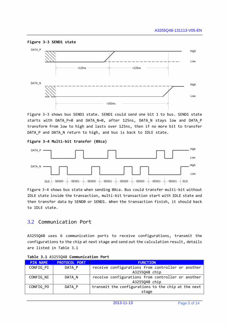
Figure 3-3 SEND1 state
DATA_P
High
Low
>125ns >125ns
DATA_N
High
Low
>250ns
Figure 3-3 shows bus SEND1 state. SEND1 could send one bit 1 to bus. SEND1 state
starts with DATA_P=0 and DATA_N=0, after 125ns, DATA_N stays low and DATA_P
transform from low to high and lasts over 125ns, then if no more bit to transfer
DATA_P and DATA_N return to high, and bus is back to IDLE state.
Figure 3-4 Multi-bit transfer (0Xca)
DATA_P High
Low
DATA_N High
Low
IDLE SEND0 SEND1 SEND0 SEND1 SEND0 SEND0 SEND1 SEND1 IDLE
Figure 3-4 shows bus state when sending 0Xca. Bus could transfer multi-bit without
IDLE state inside the transaction, multi-bit transaction start with IDLE state and
then transfer data by SEND0 or SEND1. When the transaction finish, it should back
to IDLE state.
3.2 Communication Port A3255Q48 uses 6 communication ports to receive configurations, transmit the
configurations to the chip at next stage and send out the calculation result, details
are listed in Table 3.1
Table 3.1 A3255Q48 Communication Port
PIN NAME PROTOCOL PORT FUNCTION CONFIG_PI DATA_P receive configurations from controller or another
A3255Q48 chip CONFIG_NI DATA_N receive configurations from controller or another
A3255Q48 chip CONFIG_PO DATA_P transmit the configurations to the chip at the next
stage

A3255Q48-131113-V05-EN
2013-11-13 Page 6 of 14
CONFIG_NO DATA_N transmit the configurations to the chip at the next
stage REPORT_P DATA_P send out the golden nonce when A3255Q48 get the share REPORT_N DATA_N send out the golden nonce when A3255Q48 get the share
4. DATA FORMAT
Three segments should be configured before A3255Q48 hash calculation by CONFIG_PI
and CONFIG_NI. Clock configuration segment is for adjusting clock frequency, gating
core clock or switching clock source. Hash data segment is the initial input data
of SHA256 HASH. Hash work of chips in the same chain is split by the initial nonce
segment. Configure data should send as the order shown in Figure 4-1
Figure 4-1 Configure Sequence
Initial Nonce Hash Data Clock Configuration
Last word
First word
A3255Q48-131113-V05-EN
2013-11-13 Page 7 of 14
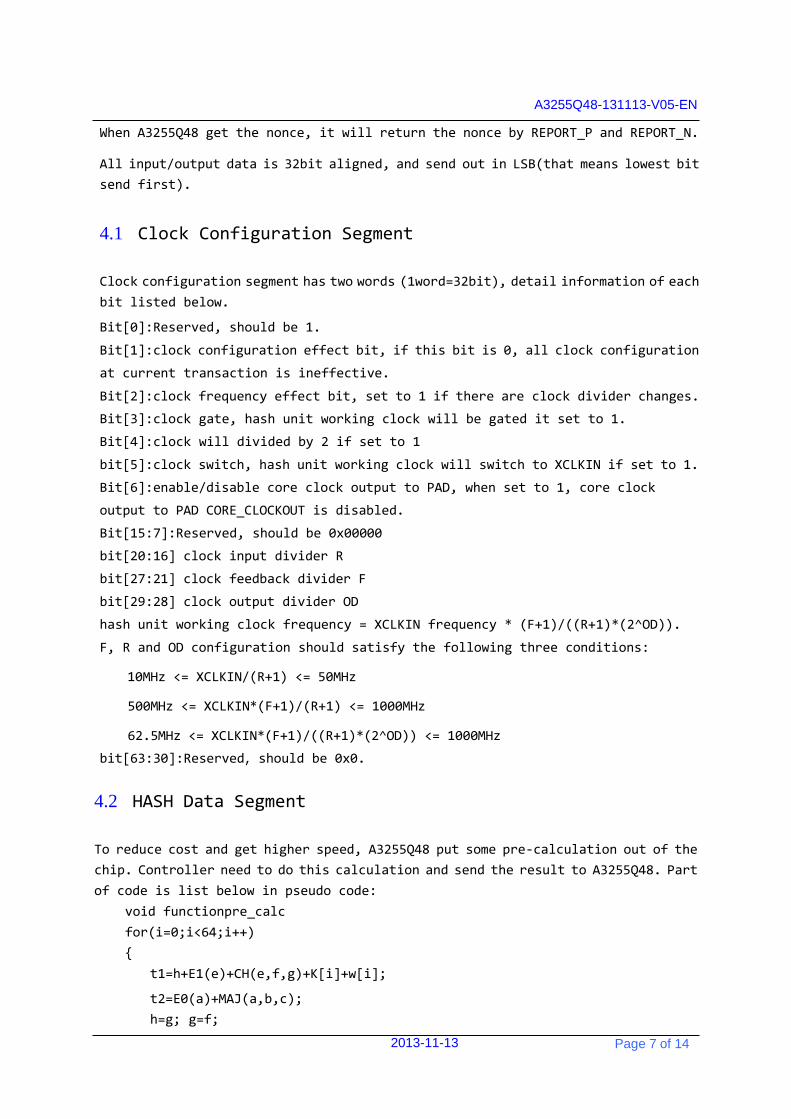
When A3255Q48 get the nonce, it will return the nonce by REPORT_P and REPORT_N. All input/output data is 32bit aligned, and send out in LSB(that means lowest bit
send first).
4.1 Clock Configuration Segment Clock configuration segment has two words (1word=32bit), detail information of each
bit listed below.
Bit[0]:Reserved, should be 1.
Bit[1]:clock configuration effect bit, if this bit is 0, all clock configuration
at current transaction is ineffective.
Bit[2]:clock frequency effect bit, set to 1 if there are clock divider changes.
Bit[3]:clock gate, hash unit working clock will be gated it set to 1.
Bit[4]:clock will divided by 2 if set to 1
bit[5]:clock switch, hash unit working clock will switch to XCLKIN if set to 1.
Bit[6]:enable/disable core clock output to PAD, when set to 1, core clock
output to PAD CORE_CLOCKOUT is disabled.
Bit[15:7]:Reserved, should be 0x00000
bit[20:16] clock input divider R
bit[27:21] clock feedback divider F
bit[29:28] clock output divider OD
hash unit working clock frequency = XCLKIN frequency * (F+1)/((R+1)*(2^OD)).
F, R and OD configuration should satisfy the following three conditions:
10MHz <= XCLKIN/(R+1) <= 50MHz
500MHz <= XCLKIN*(F+1)/(R+1) <= 1000MHz
62.5MHz <= XCLKIN*(F+1)/((R+1)*(2^OD)) <= 1000MHz
bit[63:30]:Reserved,should be 0x0.
4.2 HASH Data Segment To reduce cost and get higher speed, A3255Q48 put some pre-calculation out of the
chip. Controller need to do this calculation and send the result to A3255Q48. Part
of code is list below in pseudo code:
void functionpre_calc
for(i=0;i<64;i++)
{
t1=h+E1(e)+CH(e,f,g)+K[i]+w[i];
t2=E0(a)+MAJ(a,b,c);
h=g; g=f;

A3255Q48-131113-V05-EN
2013-11-13 Page 8 of 14
f=e;
e=d+t1;
d=c; c=b;
b=a;
a=t1+t2;
if(i=0) a0 = a;
if(i=1) a1 = a;
if(i=2) a2 = a;
if(i=0) e0 = e;
if(i=1) e1 = e;
if(i=2) e2 = e;
}
a0, a1, a2, e0, e1, e2 is the pre-calculation result should send to A3255Q48 (for
further information, please refer to http://en.wikipedia.org/wiki/SHA256).
The complete sequence of Hash Data Segment is shown in Figure 4-2
Figure 4-2 Hash Data Segment Transfer Sequence
a2 midstate e0 e1 e2 a0 a1 data
Last word
First word
All data is sent in LSB, means low bit, low byte and low word is sent first
4.3 Initial Nonce Segment Since A3255Q48 could work in chain mode, and different chips in the same chain
receive the same HASH data, so initial nonce value is the only different that could
A3255Q48-131113-V05-EN
2013-11-13 Page 9 of 14
split the work. The length of this segment is N word, N is the chain length. After
initial nonce value configuration, all A3255Q48 chips get their own initial nonce,
and then they could work at different range. For an example, if 10 chips are in
the same chain, the nonce range segment should be 10 word long, and the whole 2^32
nonce should be split to 10 different areas, the configuration is shown in Figure
4-3.
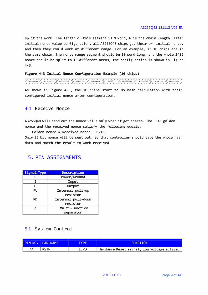
Figure 4-3 Initial Nonce Configuration Example (10 chips)
0x00000000 0x19999999 0x33333332 0x4ccccccb 0x66666664 0x7ffffffd 0x99999996 0xb333332f 0xccccccc8 0xe6666661
As shown in figure 4-3, the 10 chips start to do hash calculation with their
configured initial nonce after configuration.
4.4 Receive Nonce A3255Q48 will send out the nonce value only when it get shares. The REAL golden
nonce and the received nonce satisfy the following equals:
Golden nonce = Received nonce – 0x180
Only 32 bit nonce will be sent out, so that controller should save the whole hash
data and match the result to work received
5. PIN ASSIGNMENTS
Signal Type Description
P Power/Ground I Input O Output PU Internal pull-up
resistor PD Internal pull-down
resistor / Multi-function
separator
5.1 System Control
PIN NO.
PAD NAME
TYPE
FUNCTION
44 RSTN I,PD Hardware Reset signal, low voltage active.
A3255Q48-131113-V05-EN
2013-11-13 Page 10 of 14
PIN NO.
PAD NAME
TYPE
FUNCTION
9 XCLKIN I Crystal Clock input to chip 43 CORE_CLKOUT O Debug Clock output from chip
5.2 Function
PIN NO.
PAD NAME
TYPE
FUNCTION
1 CONFIG_PI I Config Data input to chip 2 CONFIG_NI I Config Data input to chip 36 CONFIG_PO O Config Data output from chip 35 CONFIG_NO O Config Data output from chip 16 REPORT_N O,PU Hash Data output from chip, need pull up on PCB 17 REPORT_P O,PU Hash Data output from chip, need pull up on PCB
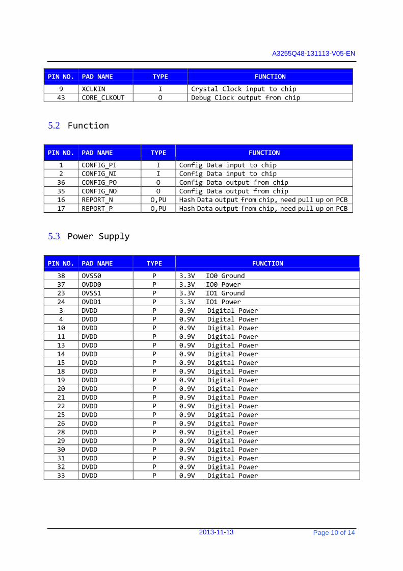
5.3 Power Supply
PIN NO.
PAD NAME
TYPE
FUNCTION
38 OVSS0 P 3.3V IO0 Ground 37 OVDD0 P 3.3V IO0 Power 23 OVSS1 P 3.3V IO1 Ground 24 OVDD1 P 3.3V IO1 Power 3 DVDD P 0.9V Digital Power 4 DVDD P 0.9V Digital Power 10 DVDD P 0.9V Digital Power 11 DVDD P 0.9V Digital Power 13 DVDD P 0.9V Digital Power 14 DVDD P 0.9V Digital Power 15 DVDD P 0.9V Digital Power 18 DVDD P 0.9V Digital Power 19 DVDD P 0.9V Digital Power 20 DVDD P 0.9V Digital Power 21 DVDD P 0.9V Digital Power 22 DVDD P 0.9V Digital Power 25 DVDD P 0.9V Digital Power 26 DVDD P 0.9V Digital Power 28 DVDD P 0.9V Digital Power 29 DVDD P 0.9V Digital Power 30 DVDD P 0.9V Digital Power 31 DVDD P 0.9V Digital Power 32 DVDD P 0.9V Digital Power 33 DVDD P 0.9V Digital Power
A3255Q48-131113-V05-EN
2013-11-13 Page 11 of 14
PIN NO.
PAD NAME
TYPE
FUNCTION
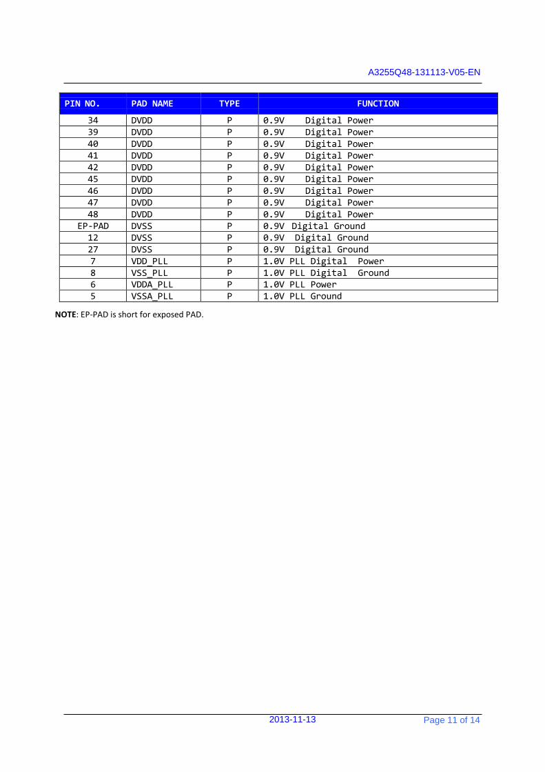
34 DVDD P 0.9V Digital Power 39 DVDD P 0.9V Digital Power 40 DVDD P 0.9V Digital Power 41 DVDD P 0.9V Digital Power 42 DVDD P 0.9V Digital Power 45 DVDD P 0.9V Digital Power 46 DVDD P 0.9V Digital Power 47 DVDD P 0.9V Digital Power 48 DVDD P 0.9V Digital Power
EP-PAD DVSS P 0.9V Digital Ground 12 DVSS P 0.9V Digital Ground 27 DVSS P 0.9V Digital Ground 7 VDD_PLL P 1.0V PLL Digital Power 8 VSS_PLL P 1.0V PLL Digital Ground 6 VDDA_PLL P 1.0V PLL Power 5 VSSA_PLL P 1.0V PLL Ground
NOTE: EP-PAD is short for exposed PAD.
A3255Q48-131113-V05-EN
2013-11-13 Page 12 of 14
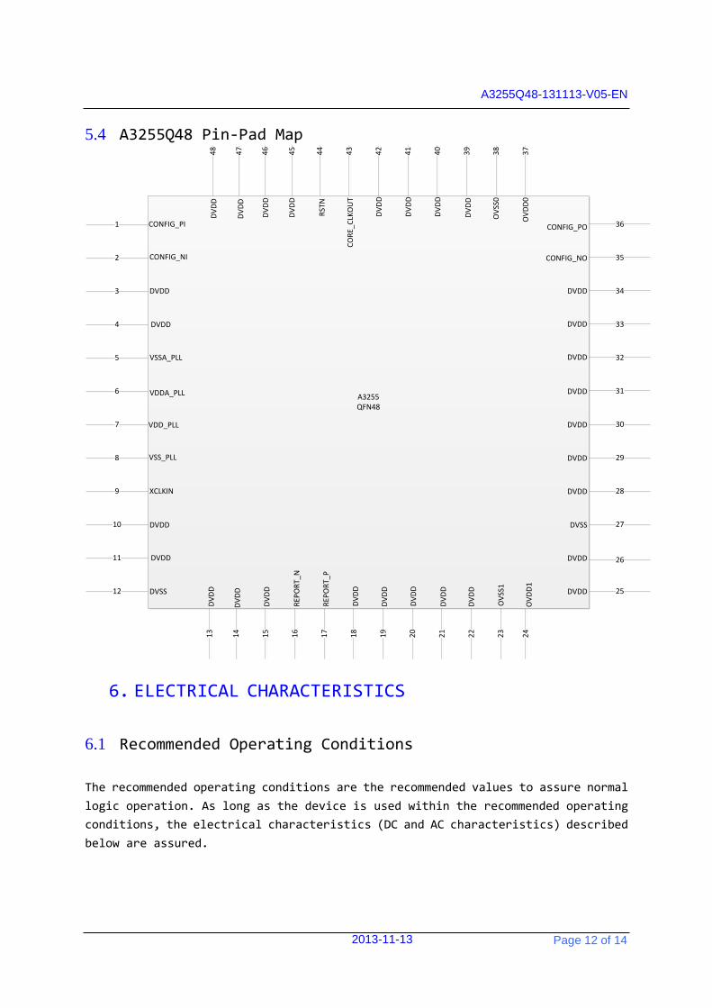
5.4 A3255Q48 Pin-Pad Map
A3255QFN48
1
2
3
VSSA_PLL
4
DVSS
5
6
7
8
9
10
11
12
VDDA_PLL
14
15
DV
DD
16
REP
OR
T_N
17
18
DV
DD
19
20
DV
DD
21
22
23
DVDD
27
DVDD
28
29
DVDD
30
DVDD
31
DVDD
32
DVDD
33
DVSS
34
DVDD
35
DVDD
36
DV
DD
26
DV
DD
25
39
40
41
DV
DD
42
CONFIG_NO
43
CONFIG_PO
44
DV
DD
37
DV
DD
38
45
46
CO
RE_
CLK
OU
T
DV
DD
DV
DD
OV
SS1
DVDD
XCLKIN
CONFIG_PI
CONFIG_NI
DVDD
DV
DD
DV
DD
DV
DD
13
24
OV
DD
1
47
RST
N
OV
SS0
48
DVDD
REP
OR
T_P
OV
DD
0
VDD_PLL
VSS_PLL
DVDD
DV
DD
DVDD
DV
DD
DV
DD
6. ELECTRICAL CHARACTERISTICS
6.1 Recommended Operating Conditions The recommended operating conditions are the recommended values to assure normal
logic operation. As long as the device is used within the recommended operating
conditions, the electrical characteristics (DC and AC characteristics) described
below are assured.

A3255Q48-131113-V05-EN
2013-11-13 Page 13 of 14
PARAMETER.
SYMBOL
MIN
TYP
MAX
UNIT
Supply Core voltage
DVDD 0.9 1.0 1.1 V
Supply 1.0V analog voltage
VDDA_PLL 0.9 1.0 1.1 V
Supply I/O voltage
OVDD 3.0 3.3 3.6 V
Maximum input voltage
V i max
--
--
3.6
V
Operating Temperature
T OPR
-20
--
+85 ℃
Storage Temperature
T STOR
-40
--
+150 ℃
Operating Current
I OP
--
--
2000
mA
Static Current I SUSP -- -- 20 mA
6.2 Oscillation
PARAMETER. CONDI TIONS
SYMBOL
MIN
TYP MAX
UNIT
Input clock frequency
--
Fclixin
--
25
--
MHz
Input clock period -- Tclkxin -- 40 -- Ns Clock duty cycle -- -- 45 50 55 % Input pad capacitance
--
--
--
3.398
--
Pf
Jitter -- -- -- -- 10 Ps Input HIGH leakage current
--
--
--
±10
uA
Input LOW leakage current
--
--
--
--
±10
uA

A3255Q48-131113-V05-EN
2013-11-13 Page 14 of 14
7. PACKAGE INFORMATION
7.1 A3255Q48 Package Specifications

A3255Q48-131113-V05-EN
2013-11-13 Page 15 of 14
8. REVISION HISTORY
Version No. Remarks Release Date 0.1 Initial version released for engineering review. 2013-09-03
0.2 Fix clock configuration descriptions 2013-09-10
0.3 Update power and speed 2013-09-29
0.4 Fix a wrong description of PLL power pin, update package information
2013-10-08
0.5 Fix PLL configuration bit R and F related formula. Add EP-PAD description in package section
2013-11-13