Variable Reluctance Sensor Interfaces with Differential ... · General Description The...
23
General Description The MAX9924–MAX9927 variable reluctance (VR or mag- netic coil) sensor interface devices are ideal for position and speed sensing for automotive crankshafts, camshafts, transmission shafts, etc. These devices inte- grate a precision amplifier and comparator with selectable adaptive peak threshold and zero-crossing circuit blocks that generate robust output pulses even in the presence of substantial system noise or extremely weak VR signals. The MAX9926/MAX9927 are dual versions of the MAX9924/MAX9925, respectively. The MAX9924/ MAX9926 combine matched resistors with a CMOS input precision operational amplifier to give high CMRR over a wide range of input frequencies and temperatures. The MAX9924/MAX9926 differential amplifiers provide a fixed gain of 1V/V. The MAX9925/MAX9927 make all three ter- minals of the internal operational amplifier available, allowing greater flexibility for gain. The MAX9926 also provides a direction output that is useful for quadrature- connected VR sensors that are used in certain high-per- formance engines. These devices interface with both new-generation differential VR sensors as well as legacy single-ended VR sensors. The MAX9924/MAX9925 are available in the 10-pin μMAX ® package, while the MAX9926/MAX9927 are available in the 16-pin QSOP package. All devices are specified over the -40°C to +125°C automotive temper- ature range. Applications Camshaft VRS Interfaces Crankshaft VRS Interfaces Vehicle Speed VRS Interfaces Features ♦ Differential Input Stage Provides Enhanced Noise Immunity ♦ Precision Amplifier and Comparator Allows Small-Signal Detection ♦ User-Enabled Internal Adaptive Peak Threshold or Flexible External Threshold ♦ Zero-Crossing Detection Provides Accurate Phase Information MAX9924–MAX9927 Variable Reluctance Sensor Interfaces with Differential Input and Adaptive Peak Threshold ________________________________________________________________ Maxim Integrated Products 1 Ordering Information 19-4283; Rev 4; 3/12 For pricing, delivery, and ordering information, please contact Maxim Direct at 1-888-629-4642, or visit Maxim’s website at www.maxim-ic.com. PART TEMP RANGE PIN-PACKAGE MAX9924 UAUB+ -40°C to +125°C 10 μMAX MAX9924 UAUB/V+ -40°C to +125°C 10 μMAX MAX9925 AUB+ -40°C to +125°C 10 μMAX MAX9926 UAEE+ -40°C to +125°C 16 QSOP MAX9926 UAEE/V+ -40°C to +125°C 16 QSOP MAX9927 AEE+ -40°C to +125°C 16 QSOP MAX9927 AEE/V+ -40°C to +125°C 16 QSOP +Denotes a lead(Pb)-free/RoHS-compliant package. /V denotes an automotive qualified part. μMAX is a registered trademark of Maxim Integrated Products, Inc. Simplified Block Diagram μC DIFFERENTIAL AMPLIFIER ADAPTIVE/MINIMUM AND ZERO-CROSSING THRESHOLDS INTERNAL/EXTERNAL BIAS VOLTAGE VR SENSOR ENGINE BLOCK MAX9924
Transcript of Variable Reluctance Sensor Interfaces with Differential ... · General Description The...

General DescriptionThe MAX9924–MAX9927 variable reluctance (VR or mag-netic coil) sensor interface devices are ideal for positionand speed sensing for automotive crankshafts,camshafts, transmission shafts, etc. These devices inte-grate a precision amplifier and comparator with selectableadaptive peak threshold and zero-crossing circuit blocksthat generate robust output pulses even in the presenceof substantial system noise or extremely weak VR signals.
The MAX9926/MAX9927 are dual versions of theMAX9924/MAX9925, respectively. The MAX9924/MAX9926 combine matched resistors with a CMOS inputprecision operational amplifier to give high CMRR over awide range of input frequencies and temperatures. TheMAX9924/MAX9926 differential amplifiers provide a fixedgain of 1V/V. The MAX9925/MAX9927 make all three ter-minals of the internal operational amplifier available,allowing greater flexibility for gain. The MAX9926 alsoprovides a direction output that is useful for quadrature-connected VR sensors that are used in certain high-per-formance engines. These devices interface with bothnew-generation differential VR sensors as well as legacysingle-ended VR sensors.
The MAX9924/MAX9925 are available in the 10-pinµMAX® package, while the MAX9926/MAX9927 areavailable in the 16-pin QSOP package. All devices arespecified over the -40°C to +125°C automotive temper-ature range.
ApplicationsCamshaft VRS Interfaces
Crankshaft VRS Interfaces
Vehicle Speed VRS Interfaces
Features� Differential Input Stage Provides Enhanced Noise
Immunity
� Precision Amplifier and Comparator AllowsSmall-Signal Detection
� User-Enabled Internal Adaptive Peak Threshold orFlexible External Threshold
� Zero-Crossing Detection Provides AccuratePhase Information
MA
X9
92
4–M
AX
99
27
Variable Reluctance Sensor Interfaces withDifferential Input and Adaptive Peak Threshold
________________________________________________________________ Maxim Integrated Products 1
Ordering Information
19-4283; Rev 4; 3/12
For pricing, delivery, and ordering information, please contact Maxim Direct at 1-888-629-4642,or visit Maxim’s website at www.maxim-ic.com.
PART TEMP RANGE PIN-PACKAGE
MAX9924UAUB+ -40°C to +125°C 10 µMAX
MAX9924UAUB/V+ -40°C to +125°C 10 µMAX
MAX9925AUB+ -40°C to +125°C 10 µMAX
MAX9926UAEE+ -40°C to +125°C 16 QSOP
MAX9926UAEE/V+ -40°C to +125°C 16 QSOP
MAX9927AEE+ -40°C to +125°C 16 QSOPMAX9927AEE/V+ -40°C to +125°C 16 QSOP
+Denotes a lead(Pb)-free/RoHS-compliant package./V denotes an automotive qualified part.
µMAX is a registered trademark of Maxim Integrated Products, Inc.
Simplified Block Diagram
μC
DIFFERENTIALAMPLIFIER
ADAPTIVE/MINIMUMAND
ZERO-CROSSINGTHRESHOLDS
INTERNAL/EXTERNALBIAS VOLTAGE
VR SENSOR
ENGINE BLOCKMAX9924
MA
X9
92
4–M
AX
99
27
Variable Reluctance Sensor Interfaces withDifferential Input and Adaptive Peak Threshold
2 _______________________________________________________________________________________
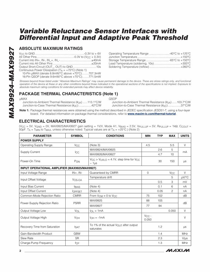
ABSOLUTE MAXIMUM RATINGS
ELECTRICAL CHARACTERISTICS(VCC = 5V, VGND = 0V, MAX9925/MAX9927 gain setting = 1V/V, Mode A1, VBIAS = 2.5V, VPULLUP = 5V, RPULLUP = 1kΩ, CCOUT =50pF. TA = TMIN to TMAX, unless otherwise noted. Typical values are at TA = +25°C.) (Note 2)
Stresses beyond those listed under “Absolute Maximum Ratings” may cause permanent damage to the device. These are stress ratings only, and functionaloperation of the device at these or any other conditions beyond those indicated in the operational sections of the specifications is not implied. Exposure toabsolute maximum rating conditions for extended periods may affect device reliability.
VCC to GND.............................................................-0.3V to + 6VAll Other Pins..............................................-0.3V to (VCC + 0.3V)Current into IN+, IN-, IN_+, IN_-.......................................±40mACurrent into All Other Pins ................................................±20mAOutput Short-Circuit (OUT_, OUT) to GND.............................10sContinuous Power Dissipation (TA = +70°C) (Note 1)
10-Pin µMAX (derate 8.8mW/°C above +70°C) ........707.3mW16-Pin QSOP (derate 9.6mW/°C above +70°C)........771.5mW
Operating Temperature Range .........................-40°C to +125°CJunction Temperature ......................................................+150°CStorage Temperature Range .............................-65°C to +150°CLead Temperature (soldering, 10s) .................................+300°CSoldering Temperature (reflow) .......................................+260°C
PARAMETER SYMBOL CONDITIONS MIN TYP MAX UNITS
POWER SUPPLY
Operating Supply Range VCC (Note 3) 4.5 5.5 V
MAX9924/MAX9925 2.6 5Supply Current ICC
MAX9926/MAX9927 4.7 10mA
Power-On Time PONVCC > VUVLO = 4.1V, step time for VCC~ 1µs
30 150 µs
INPUT OPERATIONAL AMPLIFIER (MAX9925/MAX9927)
Input Voltage Range IN+, IN- Guaranteed by CMRR 0 VCC V
Temperature drift 5 µV/°CInput Offset Voltage VOS-OA
0.5 3 mV
Input Bias Current IBIAS (Note 4) 0.1 6 nA
Input Offset Current IOFFSET (Note 4) 0.05 2 nA
Common-Mode Rejection Ratio CMRR From VCM = 0 to VCC 75 102 dB
MAX9925 88 105Power-Supply Rejection Ratio PSRR
MAX9927 77 94dB
Output Voltage Low VOL IOL = 1mA 0.050 V
Output Voltage High VOH IOH = -1mAVCC -0.050
V
Recovery Time from Saturation tSATTo 1% of the actual VOUT after outputsaturates
1.2 µs
Gain-Bandwidth Product GBW 1.4 MHz
Slew Rate SR 2.3 V/µs
Charge-Pump Frequency fCP 1.3 MHz
Note 1: Package thermal resistances were obtained using the method described in JEDEC specification JESD51-7, using a four-layerboard. For detailed information on package thermal considerations, refer to www.maxim-ic.com/thermal-tutorial.
µMAXJunction-to-Ambient Thermal Resistance (θJA) ......113.1°C/WJunction-to-Case Thermal Resistance (θJC) ................42°C/W
QSOPJunction-to-Ambient Thermal Resistance (θJA) ......103.7°C/WJunction-to-Case Thermal Resistance (θJC) ................37°C/W
PACKAGE THERMAL CHARACTERISTICS (Note 1)

MA
X9
92
4–M
AX
99
27
Variable Reluctance Sensor Interfaces withDifferential Input and Adaptive Peak Threshold
_______________________________________________________________________________________ 3
PARAMETER SYMBOL CONDITIONS MIN TYP MAX UNITS
INPUT DIFFERENTIAL AMPLIFIER (MAX9924/MAX9926)
Input Voltage Range IN+, IN- Guaranteed by CMRR -0.3VCC +
0.3V
MAX9924 (Note 5) 60 87Differential AmplifierCommon-Mode Rejection Ratio
CMRRMAX9926 (Note 5) 55 78
dB
Input Resistance RIN (Note 5) 65 100 135 kΩADAPTIVE PEAK DETECTION
MAX9924/MAX9925 -6.5 0 +6.5Zero-Crossing Threshold VZERO_THRESH
Mode Boperation(Notes 5, 6) MAX9926/MAX9927 -6.5 0 +10
mV
VADAPTIVE Adaptive peak threshold 33 %PK
Minimum threshold of hysteresiscomparator MAX9924/MAX9926(Notes 5, 6)
4 15 30
Minimum threshold of hysteresiscomparator MAX9925/MAX9927(Notes 5, 6)
20 30 50
VMIN-THRESH - VZERO-THRESH forMAX9924 (Notes 5, 6)
7 15 26
VMIN-THRESH - VZERO-THRESH forMAX9926 (Notes 5, 6)
2 15 30
Fixed and Adaptive PeakThreshold VMIN-THRESH
VMIN-THRESH - VZERO-THRESH forMAX9925/MAX9927 (Notes 5, 6)
19 30 50
mV
Watchdog Timeout for AdaptivePeak Threshold
tWD
Timing window to reset the adaptivepeak threshold if not triggered (inputlevel below threshold)
45 85 140 ms
ENTIRE SYSTEM
Comparator Output Low Voltage VCOUT_OL 0.2 V
tPDZ Overdrive = 2V to 3V, zero-crossing 50Propagation Delay
tPDA Overdrive = 2V to 3V, adaptive peak 150ns
COUT Transition Time tHL-LH 2 ns
Propagation Delay Jitter tPD-JITTER
Includes noise of differential amplifierand comparator, f = 10kHz,VIN = 1VP-P sine wave
20 ns
ELECTRICAL CHARACTERISTICS (continued)(VCC = 5V, VGND = 0V, MAX9925/MAX9927 gain setting = 1V/V, Mode A1, VBIAS = 2.5V, VPULLUP = 5V, RPULLUP = 1kΩ, CCOUT =50pF. TA = TMIN to TMAX, unless otherwise noted. Typical values are at TA = +25°C.) (Note 2)
MA
X9
92
4–M
AX
99
27
Variable Reluctance Sensor Interfaces withDifferential Input and Adaptive Peak Threshold
4 _______________________________________________________________________________________
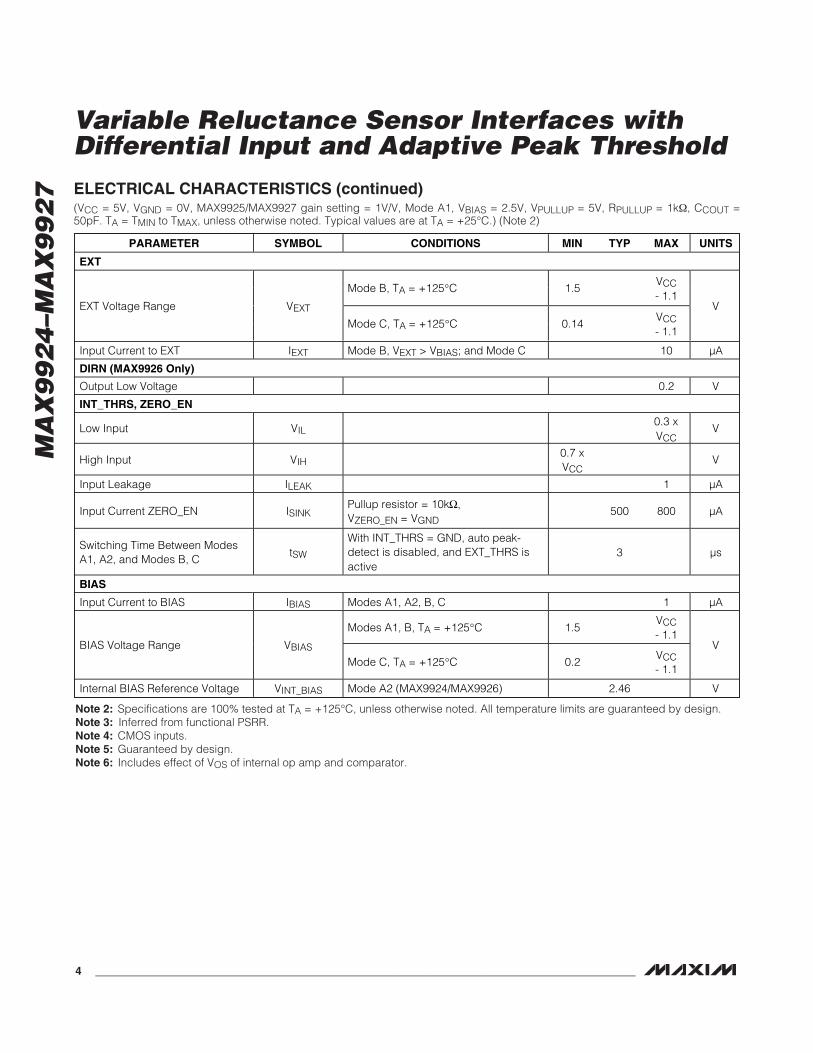
PARAMETER SYMBOL CONDITIONS MIN TYP MAX UNITS
EXT
Mode B, TA = +125°C 1.5VCC- 1.1
EXT Voltage Range VEXT
Mode C, TA = +125°C 0.14VCC- 1.1
V
Input Current to EXT IEXT Mode B, VEXT > VBIAS; and Mode C 10 µA
DIRN (MAX9926 Only)
Output Low Voltage 0.2 V
INT_THRS, ZERO_EN
Low Input VIL0.3 xVCC
V
High Input VIH0.7 xVCC
V
Input Leakage ILEAK 1 µA
Input Current ZERO_EN ISINKPullup resistor = 10kΩ,VZERO_EN = VGND
500 800 µA
Switching Time Between ModesA1, A2, and Modes B, C
tSW
With INT_THRS = GND, auto peak-detect is disabled, and EXT_THRS isactive
3 µs
BIAS
Input Current to BIAS IBIAS Modes A1, A2, B, C 1 µA
Modes A1, B, TA = +125°C 1.5VCC- 1.1
BIAS Voltage Range VBIAS
Mode C, TA = +125°C 0.2VCC- 1.1
V
Internal BIAS Reference Voltage VINT_BIAS Mode A2 (MAX9924/MAX9926) 2.46 V
ELECTRICAL CHARACTERISTICS (continued)(VCC = 5V, VGND = 0V, MAX9925/MAX9927 gain setting = 1V/V, Mode A1, VBIAS = 2.5V, VPULLUP = 5V, RPULLUP = 1kΩ, CCOUT =50pF. TA = TMIN to TMAX, unless otherwise noted. Typical values are at TA = +25°C.) (Note 2)
Note 2: Specifications are 100% tested at TA = +125°C, unless otherwise noted. All temperature limits are guaranteed by design.Note 3: Inferred from functional PSRR.Note 4: CMOS inputs.Note 5: Guaranteed by design.Note 6: Includes effect of VOS of internal op amp and comparator.
MA
X9
92
4–M
AX
99
27
Variable Reluctance Sensor Interfaces withDifferential Input and Adaptive Peak Threshold
_______________________________________________________________________________________ 5
0
5
10
15
20INPUT OFFSET VOLTAGE DISTRIBUTION
MAX
9924
toc0
1
INPUT OFFSET VOLTAGE (μV)
PERC
ENTA
GE O
F UN
ITS
(%)
-2000-500
0-1500
-1000500
10001500
30002500
2000
VCM = 0BIN SIZE = 250
0
0.1
0.3
0.2
0.4
0.5
-0.5 1.50.5 2.5 3.5 4.5 5.5
INPUT OFFSET VOLTAGEvs. INPUT COMMON-MODE VOLTAGE
MAX
9924
toc0
2
INPUT COMMON-MODE VOLTAGE (V)
INPU
T OF
FSET
VOL
TAGE
(mV)
VOUT = 2.5VMAX9925
COMMON-MODE REJECTION RATIOvs. FREQUENCY
MAX
9924
toc0
3
FREQUENCY (Hz)
CMRR
(dB)
10k1k10010
20
40
60
80
100
120
01 100k
VBIAS = VOUT = 2.5VVCM = 2VP-PCMRR = 20log(ADM/ACM)
POWER-SUPPLY REJECTION RATIOvs. FREQUENCY
MAX
9924
toc0
4
FREQUENCY (Hz)
PSSR
(dB)
10k1k10010
-100
-80
-60
-40
-20
0
-110
-90
-70
-50
-30
-10
-1201 100k
VRIPPLE = 100mVP-PVBIAS = VOUT = 2.5VINPUTS COUPLED TO GND
OPEN LOOP FREQUENCYRESPONSE
MAX
9924
toc0
5
FREQUENCY (kHz)
GAIN
(dB)
0.1
25
50
75
100
125
00.001 10
VCC = 5VVBIAS = 2.5VVOUT = 2VP-PMAX9925
VOL AND VOH vs. TEMPERATURE
MAX
9924
toc0
6
TEMPERATURE (°C)
V OL A
ND V
OH (m
V)
50 75 100250-25
15
20
40
5
10
25
30
35
0-50 125
VCC - VOH
VOL
0
0.2
0.1
0.4
0.3
0.5
0.6
-50 25 50-25 0 75 100 125
INPUT OFFSET VOLTAGEvs. TEMPERATURE
MAX
9924
toc0
7
TEMPERATURE (°C)
INPU
T OF
FSET
VOL
TAGE
(mV)
VCM = 0
VOUT = 2.5VMAX9925
VCM = 2.5V
ADAPTIVE THRESHOLD AND RATIOvs. SIGNAL LEVEL
MAX
9924
toc0
8
SIGNAL LEVEL (VP)
ADAP
TIVE
THR
ESHO
LD L
EVEL
(mV)
1.5 2.01.00.5
400
500
900
100
200
300
600
700
800
00 2.5
fIN = 1kHzMAX9924
ADAPTIVE THRESHOLDvs. TEMPERATURE
MAX
9924
toc0
9
TEMPERATURE (°C)
THRE
SHOL
D (m
V)
25 50 75 1000-25
200
250
400
50
100
150
300
350
0-50 125
VIN = 2VP-PfIN = 1kHzMAX9924
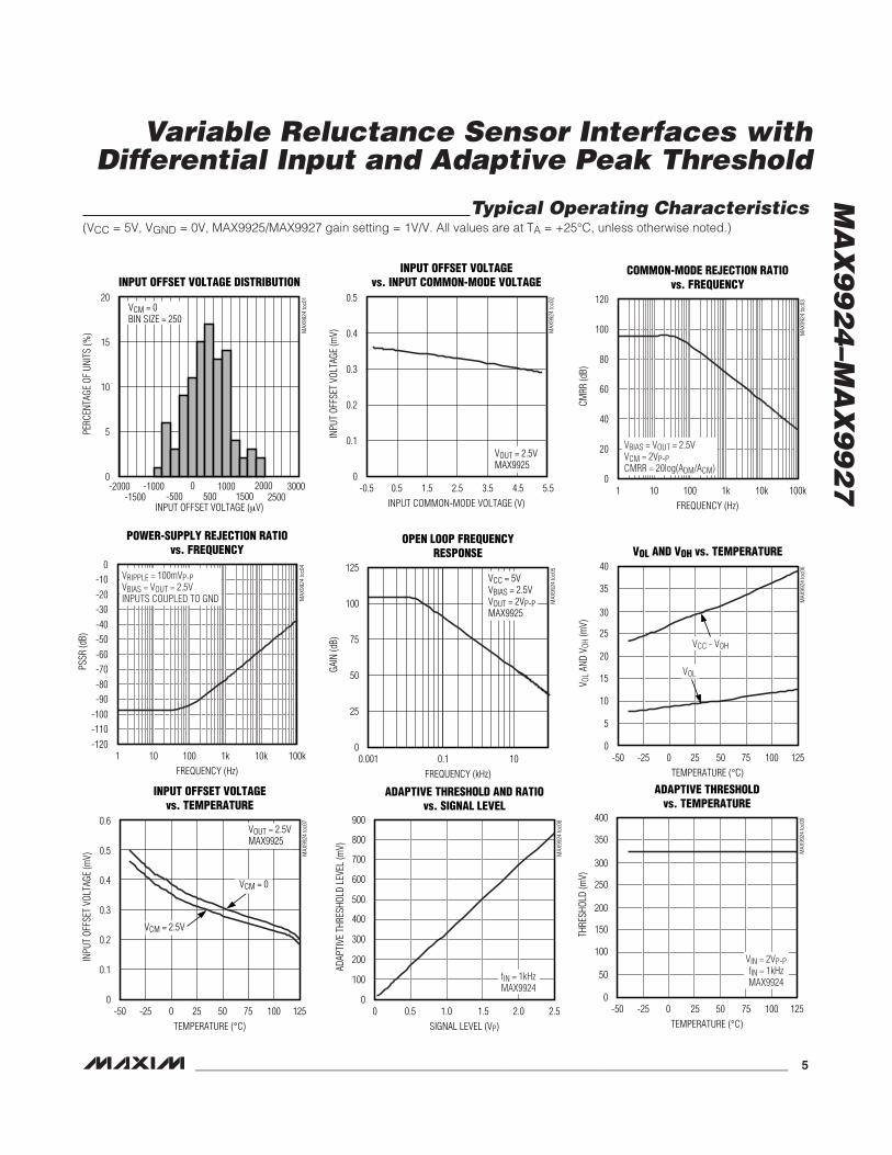
Typical Operating Characteristics(VCC = 5V, VGND = 0V, MAX9925/MAX9927 gain setting = 1V/V. All values are at TA = +25°C, unless otherwise noted.)
MA
X9
92
4–M
AX
99
27
Variable Reluctance Sensor Interfaces withDifferential Input and Adaptive Peak Threshold
6 _______________________________________________________________________________________
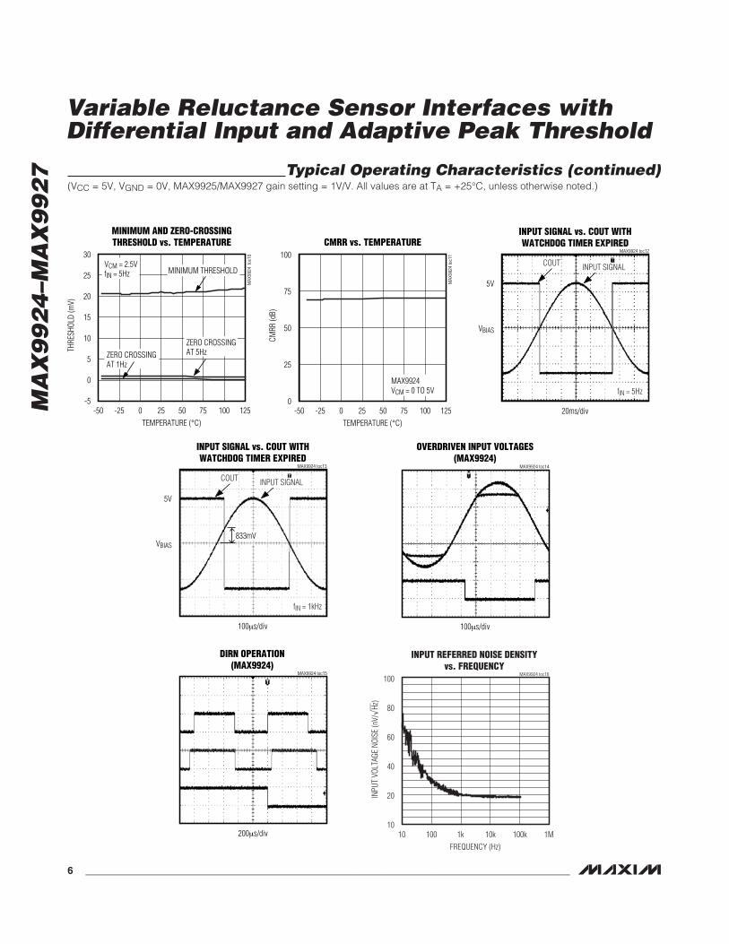
Typical Operating Characteristics (continued)(VCC = 5V, VGND = 0V, MAX9925/MAX9927 gain setting = 1V/V. All values are at TA = +25°C, unless otherwise noted.)
-5
5
0
15
10
25
20
30
-50 0 25-25 50 75 100 125
MINIMUM AND ZERO-CROSSINGTHRESHOLD vs. TEMPERATURE
MAX
9924
toc
10
TEMPERATURE (°C)
THRE
SHOL
D (m
V)
VCM = 2.5VfIN = 5Hz
ZERO CROSSINGAT 5Hz
MINIMUM THRESHOLD
ZERO CROSSINGAT 1Hz
0
25
50
75
100CMRR vs. TEMPERATURE
MAX
9924
toc1
1
TEMPERATURE (°C)
CMRR
(dB)
-50 25 50-25 0 75 100 125
MAX9924VCM = 0 TO 5V
INPUT SIGNAL vs. COUT WITHWATCHDOG TIMER EXPIRED
MAX9924 toc12
20ms/div
VBIAS
5V
fIN = 5Hz
COUT INPUT SIGNAL
INPUT SIGNAL vs. COUT WITHWATCHDOG TIMER EXPIRED
MAX9924 toc13
100μs/div
VBIAS
5V
fIN = 1kHz
COUT INPUT SIGNAL
833mV
MAX9924 toc14
100μs/div
OVERDRIVEN INPUT VOLTAGES(MAX9924)
MAX9924 toc15
200μs/div
DIRN OPERATION(MAX9924)
MAX9924 toc16
INPUT REFERRED NOISE DENSITYvs. FREQUENCY
10
20
60
40
80
100
10 1k100 10k 100k 1MFREQUENCY (Hz)
INPU
T VO
LTAG
E NO
ISE
(nV/
Hz
)

MA
X9
92
4–M
AX
99
27
Variable Reluctance Sensor Interfaces withDifferential Input and Adaptive Peak Threshold
_______________________________________________________________________________________ 7
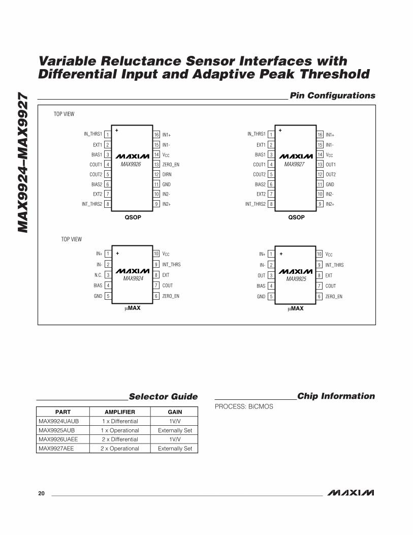
Pin DescriptionPIN
MAX9924 MAX9925 MAX9926 MAX9927NAME FUNCTION
1 1 — — IN+ Noninverting Input
2 2 — — IN- Inverting Input
— 3 — — OUT Amplifier Output
3 — — — N.C. No Connection. Not internally connected.
4 4 — — BIASInput Bias. Connect to an external resistor-divider and bypassto ground with a 0.1µF and 10µF capacitor.
5 5 11 11 GND Ground
6 6 13 — ZERO_ENZero-Crossing Enable. Mode configuration pin, internallypulled up to VCC with 10kΩ resistor.
7 7 — — COUTComparator Output. Open-drain output, connect a 10kΩ pullupresistor from COUT to VPULLUP.
8 8 — — EXTExternal Reference Input. Leave EXT unconnected in ModesA1, A2. Apply an external voltage in Modes B, C.
9 9 — — INT_THRS Internal Adaptive Threshold. Mode configuration pin.
10 10 14 14 VCC Power Supply
— — 1 1 INT_THRS1 Internal Adaptive Threshold 1. Mode configuration pin.
— — 2 2 EXT1External Reference Input 1. Leave EXT unconnected in ModesA1, A2. Apply an external voltage in Modes B, C.
— — 3 3 BIAS1Input Bias 1. Connect to an external resistor-divider andbypass to ground with a 0.1µF and 10µF capacitor.
— — 4 4 COUT1Comparator Output 1. Open-drain output, connect a 10kΩpullup resistor from COUT1 to VPULLUP.
— — 5 5 COUT2Comparator Output 2. Open-drain output, connect a 10kΩpullup resistor from COUT2 to VPULLUP.
— — 6 6 BIAS2Input Bias 2. Connect to an external resistor-divider andbypass to ground with a 0.1µF and 10µF capacitor.
— — 7 7 EXT2External Reference Input 2. Leave EXT unconnected in ModesA1, A2. Apply an external voltage in Modes B, C.
— — 8 8 INT_THRS2 Internal Adaptive Threshold 2. Mode configuration pin.
— — 9 9 IN2+ Noninverting Input 2
— — 10 10 IN2- Inverting Input 2
— — 12 — DIRNRotational Direction Output. Open-drain output, connect apullup resistor from DIRN to VPULLUP.
— — — 12 OUT2 Amplifier Output 2
— — — 13 OUT1 Amplifier Output 1
— — 15 15 IN1- Noninverting Input 1
— — 16 16 IN1+ Inverting Input 1
MA
X9
92
4–M
AX
99
27
Variable Reluctance Sensor Interfaces withDifferential Input and Adaptive Peak Threshold
8 _______________________________________________________________________________________
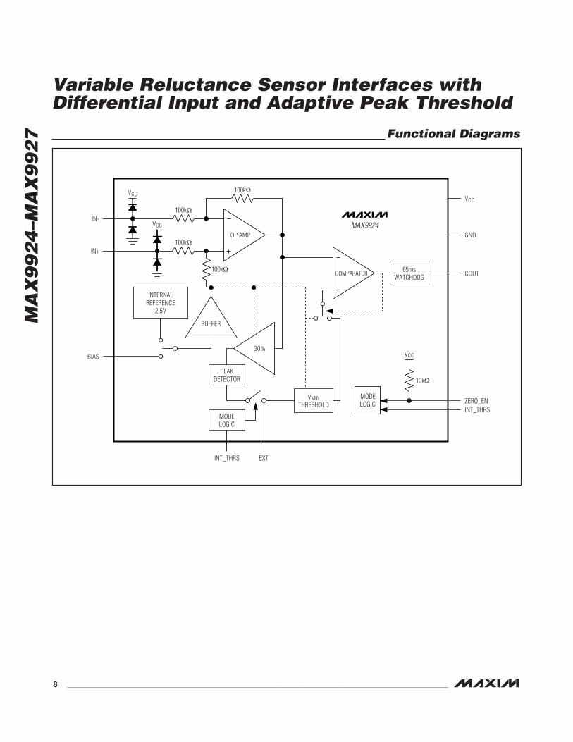
Functional Diagrams
MAX9924
100kΩ
100kΩ
10kΩ
100kΩ
VCC
VCC
MODELOGIC
INT_THRS EXT
IN-
100kΩ
VCC
IN+
BIAS
OP AMP
COMPARATOR
30%
BUFFER
INTERNALREFERENCE
2.5V
VMINTHRESHOLD
65msWATCHDOG
PEAKDETECTOR
MODELOGIC
COUT
ZERO_ENINT_THRS
GND
VCC

MA
X9
92
4–M
AX
99
27
Variable Reluctance Sensor Interfaces withDifferential Input and Adaptive Peak Threshold
_______________________________________________________________________________________ 9
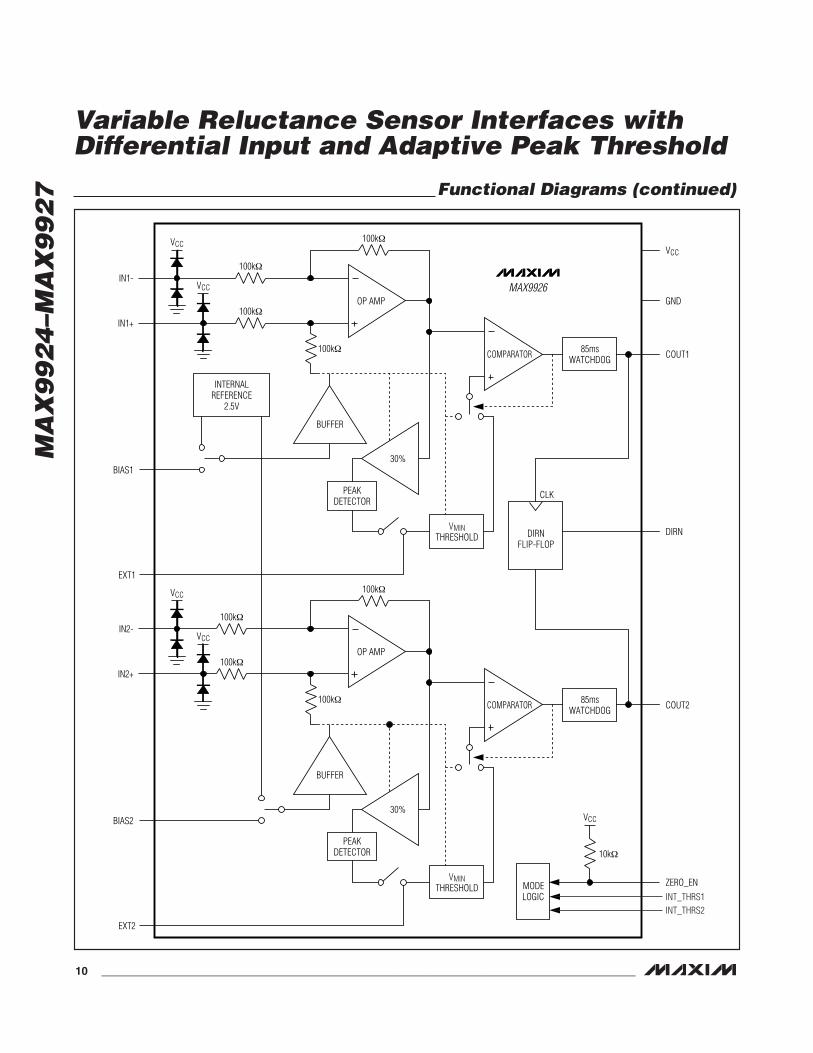
Functional Diagrams (continued)
MAX9925
10kΩ
VCC
VCC
MODELOGIC
EXT
IN-VCC
IN+
BIAS
OP AMP
COMPARATOR
30%
BUFFER
VMINTHRESHOLD
85msWATCHDOG
PEAKDETECTOR
COUT
ZERO_EN
GND
OUT
VCC
INT_THRS
MA
X9
92
4–M
AX
99
27
Variable Reluctance Sensor Interfaces withDifferential Input and Adaptive Peak Threshold
10 ______________________________________________________________________________________
Functional Diagrams (continued)
MAX9926
100kΩ
100kΩ
10kΩ
100kΩ
VCC
VCC
MODELOGIC
IN1-
100kΩ
VCC
IN1+
BIAS1
OP AMP
COMPARATOR
30%
BUFFER
INTERNALREFERENCE
2.5V
VMINTHRESHOLD
85msWATCHDOG
PEAKDETECTOR
EXT1
COUT1
ZERO_EN
GND
VCC
100kΩ
100kΩ
100kΩ
VCC
IN2-
100kΩ
VCC
IN2+
BIAS2
OP AMP
COMPARATOR
30%
BUFFER
VMINTHRESHOLD
85msWATCHDOG
PEAKDETECTOR
EXT2
COUT2
DIRNDIRNFLIP-FLOP
CLK
INT_THRS1INT_THRS2
MA
X9
92
4–M
AX
99
27
Variable Reluctance Sensor Interfaces withDifferential Input and Adaptive Peak Threshold
______________________________________________________________________________________ 11
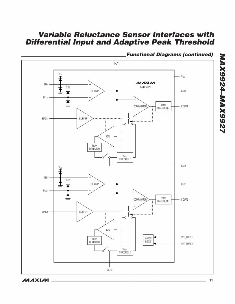
Functional Diagrams (continued)
MAX9927
VCC
IN1-VCC
IN1+
BIAS1
OP AMP
COMPARATOR
30%
BUFFER
VMINTHRESHOLD
85msWATCHDOG
PEAKDETECTOR
COUT1
EXT1
GND
OUT1
VCC
VCC
IN2-VCC
IN2+
BIAS2
OP AMP
COMPARATOR
30%
BUFFER
VMINTHRESHOLD
85msWATCHDOG
PEAKDETECTOR
COUT2
OUT1
EXT2
MODELOGIC
INT_THRS2
INT_THRS1
MA
X9
92
4–M
AX
99
27
Variable Reluctance Sensor Interfaces withDifferential Input and Adaptive Peak Threshold
12 ______________________________________________________________________________________
Detailed DescriptionThe MAX9924–MAX9927 interface with variable reluc-tance (VR) or magnetic coil sensors. These devicesproduce accurate pulses aligned with flywheel gear-teeth even when the pickup signal is small and in thepresence of large amounts of system noise. They inter-face with new-generation differential VR sensors as wellas legacy single-ended VR sensors.
The MAX9924/MAX9925 integrate a precision op amp,a precision comparator, an adaptive peak thresholdblock, a zero-crossing detection circuit, and precisionmatched resistors (MAX9924). The MAX9926 andMAX9927 are dual versions of the MAX9924 andMAX9925, respectively. The MAX9926 also provides arotational output that is useful for quadrature-connectedVR sensors used in certain high-performance engines.
The input op amp in the MAX9925/MAX9927 are typical-ly configured as a differential amplifier by using fourexternal resistors (the MAX9924/MAX9926 integrateprecision-matched resistors to give superior CMRR per-formance). This input differential amplifier rejects inputcommon-mode noise and converts the input differentialsignal from a VR sensor into a single-ended signal. Theinternal comparator produces output pulses by compar-
ing the output of the input differential amplifier with athreshold voltage that is set depending on the modethat the device is in (see the Mode Selection section).
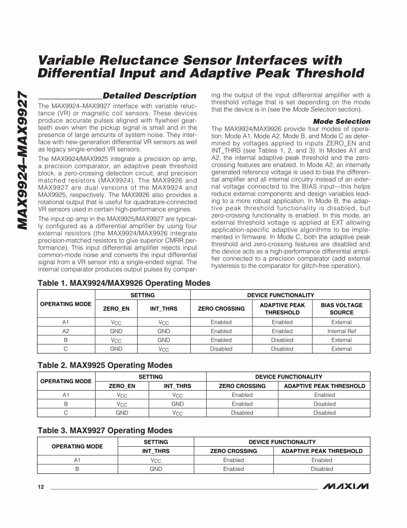
Mode SelectionThe MAX9924/MAX9926 provide four modes of opera-tion: Mode A1, Mode A2, Mode B, and Mode C as deter-mined by voltages applied to inputs ZERO_EN andINT_THRS (see Tables 1, 2, and 3). In Modes A1 andA2, the internal adaptive peak threshold and the zero-crossing features are enabled. In Mode A2, an internallygenerated reference voltage is used to bias the differen-tial amplifier and all internal circuitry instead of an exter-nal voltage connected to the BIAS input—this helpsreduce external components and design variables lead-ing to a more robust application. In Mode B, the adap-tive peak threshold functionality is disabled, butzero-crossing functionality is enabled. In this mode, anexternal threshold voltage is applied at EXT allowingapplication-specific adaptive algorithms to be imple-mented in firmware. In Mode C, both the adaptive peakthreshold and zero-crossing features are disabled andthe device acts as a high-performance differential ampli-fier connected to a precision comparator (add externalhysteresis to the comparator for glitch-free operation).
Table 1. MAX9924/MAX9926 Operating ModesSETTING DEVICE FUNCTIONALITY
OPERATING MODEZERO_EN INT_THRS ZERO CROSSING
ADAPTIVE PEAKTHRESHOLD
BIAS VOLTAGESOURCE
A1 VCC VCC Enabled Enabled External
A2 GND GND Enabled Enabled Internal Ref
B VCC GND Enabled Disabled External
C GND VCC Disabled Disabled External
Table 2. MAX9925 Operating ModesSETTING DEVICE FUNCTIONALITY
OPERATING MODEZERO_EN INT_THRS ZERO CROSSING ADAPTIVE PEAK THRESHOLD
A1 VCC VCC Enabled Enabled
B VCC GND Enabled Disabled
C GND VCC Disabled Disabled
Table 3. MAX9927 Operating ModesSETTING DEVICE FUNCTIONALITY
OPERATING MODEINT_THRS ZERO CROSSING ADAPTIVE PEAK THRESHOLD
A1 VCC Enabled Enabled
B GND Enabled Disabled
Differential AmplifierThe input operational amplifier is a rail-to-rail input andoutput precision amplifier with CMOS input bias cur-rents, low offset voltage (VOS) and drift. A novel inputarchitecture eliminates crossover distortion at the oper-ational amplifier inputs normally found in rail-to-rail inputstructures. These features enable reliable small-signaldetection for VR sensors.
The MAX9924/MAX9926 include on-chip precision-matched low-ppm resistors configured as a differentialamplifier. High-quality matching and layout of theseresistors produce extremely high DC and AC CMRRthat is important to maintain noise immunity. Thematched ppm-drift of the resistors guarantees perfor-mance across the entire -40°C to +125°C automotivetemperature range.
Bias ReferenceIn Modes A1, B, and C, a well-decoupled externalresistor-divider generates a VCC/2 signal for the BIASinput that is used to reference all internal electronics inthe device. BIAS should be bypassed with a 0.1µF and10µF capacitor in parallel with the lower half of theresistor-divider forming a lowpass filter to provide a sta-ble external BIAS reference.
The minimum threshold, adaptive peak threshold, zero-crossing threshold signals are all referenced to thisvoltage. An input buffer eliminates loading of resistor-dividers due to differential amplifier operation. ConnectBIAS to ground when operating in Mode A2. An internal(2.5V typical) reference is used in Mode A2, eliminatingexternal components.
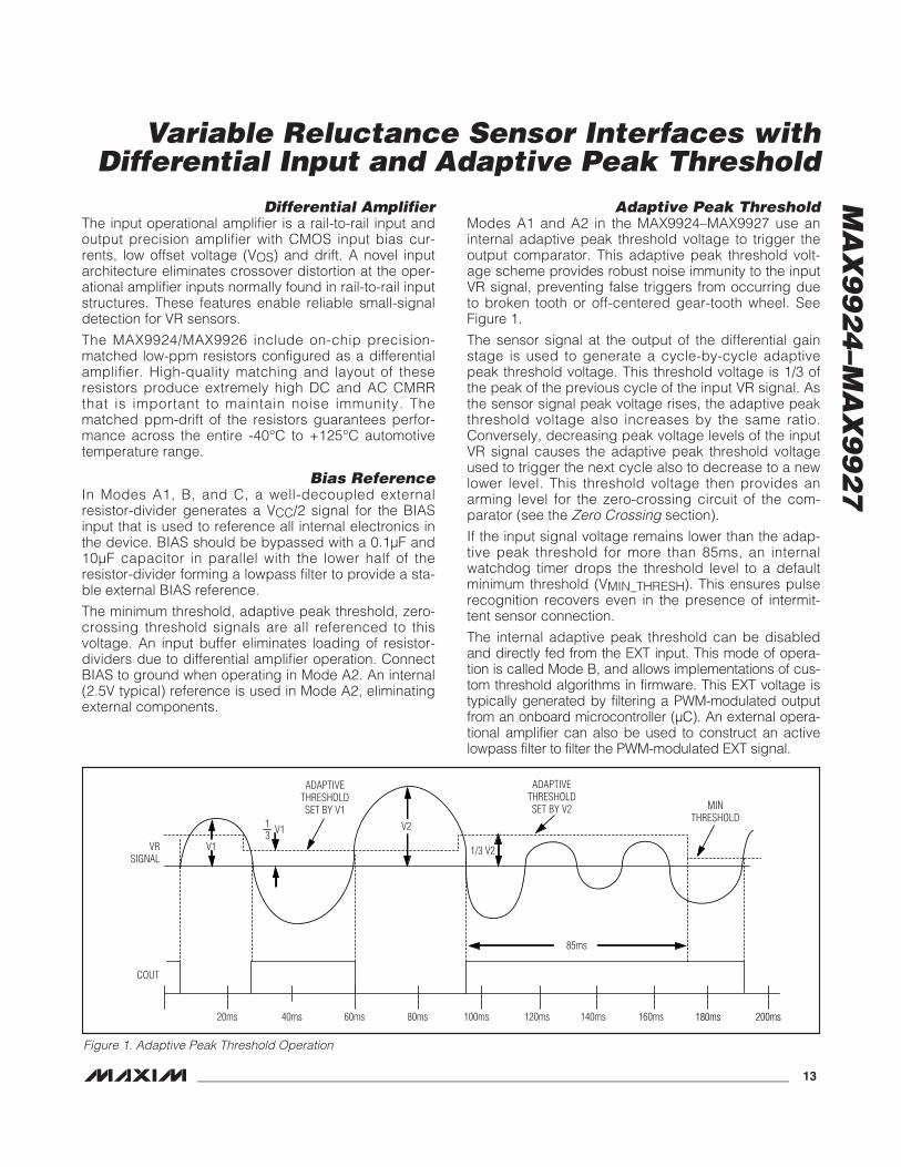
Adaptive Peak ThresholdModes A1 and A2 in the MAX9924–MAX9927 use aninternal adaptive peak threshold voltage to trigger theoutput comparator. This adaptive peak threshold volt-age scheme provides robust noise immunity to the inputVR signal, preventing false triggers from occurring dueto broken tooth or off-centered gear-tooth wheel. SeeFigure 1.
The sensor signal at the output of the differential gainstage is used to generate a cycle-by-cycle adaptivepeak threshold voltage. This threshold voltage is 1/3 ofthe peak of the previous cycle of the input VR signal. Asthe sensor signal peak voltage rises, the adaptive peakthreshold voltage also increases by the same ratio.Conversely, decreasing peak voltage levels of the inputVR signal causes the adaptive peak threshold voltageused to trigger the next cycle also to decrease to a newlower level. This threshold voltage then provides anarming level for the zero-crossing circuit of the com-parator (see the Zero Crossing section).
If the input signal voltage remains lower than the adap-tive peak threshold for more than 85ms, an internalwatchdog timer drops the threshold level to a defaultminimum threshold (VMIN_THRESH). This ensures pulserecognition recovers even in the presence of intermit-tent sensor connection.
The internal adaptive peak threshold can be disabledand directly fed from the EXT input. This mode of opera-tion is called Mode B, and allows implementations of cus-tom threshold algorithms in firmware. This EXT voltage istypically generated by filtering a PWM-modulated outputfrom an onboard microcontroller (µC). An external opera-tional amplifier can also be used to construct an activelowpass filter to filter the PWM-modulated EXT signal.
MA
X9
92
4–M
AX
99
27
Variable Reluctance Sensor Interfaces withDifferential Input and Adaptive Peak Threshold
______________________________________________________________________________________ 13
20ms
V1
40ms 60ms
COUT
VRSIGNAL
ADAPTIVETHRESHOLDSET BY V1
ADAPTIVETHRESHOLDSET BY V2 MIN
THRESHOLD
80ms 100ms 120ms 140ms 160ms
85ms
V113
V2
1/3 V2
180ms 200ms
Figure 1. Adaptive Peak Threshold Operation
MA
X9
92
4–M
AX
99
27 Zero Crossing
The zero-crossing signal provides true timing informa-tion for engine-control applications. The zero-voltagelevel in the VR sensor signal corresponds to the centerof the gear-tooth and is the most reliable marker forposition/angle-sensing applications. Since the output ofthe differential amplifier is level-shifted to the BIAS volt-age, the zero of the input VR signal is simply BIAS. Thecomparator output state controls the status of the inputswitch that changes the voltage at its noninverting inputfrom the adaptive/external threshold level to the BIASlevel. The difference in these two voltages then effec-tively acts as hysteresis for the comparator, thus pro-viding noise immunity.
ComparatorThe internal comparator is a fast open-drain outputcomparator with low input offset voltage and drift. Thecomparator precision affects the ability of the signalchain to resolve small VR sensor signals. An open-drainoutput allows the comparator to easily interface to avariety of µC I/O voltages.
When operating the MAX9924/MAX9925/MAX9926 inMode C, external hysteresis can be provided by addingexternal resistors (see Figures 5 and 8). The high andlow hysteresis thresholds in Mode C can be calculatedusing the following equations,
and
Rotational Direction Output (MAX9926 Only)
For quadrature-connected VR sensors, the open-drainoutput DIRN indicates the rotational direction of inputsIN1 and IN2 based on the output state of COUT1 andCOUT2. DIRN goes high when COUT1 is leadingCOUT2, and low when COUT1 is following COUT2.
Applications InformationBypassing and Layout Considerations
Good power-supply decoupling with high-qualitybypass capacitors is always important for precisionanalog circuits. The use of an internal charge pump forthe front-end amplifier makes this more important.Bypass capacitors create a low-impedance path toground for noise present on the power supply.
The minimum impedance of a capacitor is limited to theeffective series resistance (ESR) at the self-resonancefrequency, where the effective series inductance (ESL)cancels out the capacitance. The ESL of the capacitordominates past the self-resonance frequency resultingin a rise in impedance at high frequencies.
Bypass the power supply of the MAX9924–MAX9927with multiple capacitor values in parallel to ground. Theuse of multiple values ensures that there will be multipleself-resonance frequencies in the bypass network, low-ering the combined impedance over frequency. It isrecommended to use low-ESR and low-ESL ceramicsurface-mount capacitors in a parallel combination of10nF, 0.1µF and 1µF, with the 10nF placed closestbetween the VCC and GND pins. The connectionbetween these capacitor terminals and the power-sup-ply pins of the part (both VCC and GND) should bethrough wide traces (preferably planes), and withoutvias in the high-frequency current path.
VR
R RVTL BIAS=
+⎛⎝⎜
⎞⎠⎟ ×
21 2
VR V VR R R
VTHPULLUP BIAS
PULLUPBIAS=
−
+ +
⎛
⎝⎜
⎞
⎠⎟ +
11 2( )
Variable Reluctance Sensor Interfaces withDifferential Input and Adaptive Peak Threshold
14 ______________________________________________________________________________________

MA
X9
92
4–M
AX
99
27
Variable Reluctance Sensor Interfaces withDifferential Input and Adaptive Peak Threshold
______________________________________________________________________________________ 15
Application Circuits
IN+
IN-
BIAS
VCC
ZERO_EN INT_THRS GND
COUT
EXT
TPU
μC
VPULLUP
RPULLUP1nF
10kΩ
10kΩ
VRSENSOR
+5V
1kΩ1kΩ10μF || 0.1μF
MAX9924MAX9926
Figure 2. MAX9924/MAX9926 Operating Mode A1
IN+
IN-
BIAS
VCC
ZERO_EN INT_THRS GND
COUT
EXT
TPU
μC
VPULLUP
RPULLUP1nF
10kΩ
10kΩ
VRSENSOR
+5V
MAX9924MAX9926
Figure 3. MAX9924/MAX9926 Operating Mode A2
MA
X9
92
4–M
AX
99
27
Variable Reluctance Sensor Interfaces withDifferential Input and Adaptive Peak Threshold
16 ______________________________________________________________________________________
Application Circuits (continued)
IN+
IN-
BIAS
VCC
ZERO_EN INT_THRS GND
COUT
EXT
TPU
PWM
μC
VPULLUP
RPULLUP1nF
10kΩ
10kΩ
VRSENSOR
+5V
1kΩ1kΩ10μF || 0.1μF
MAX9924MAX9926
FILTER
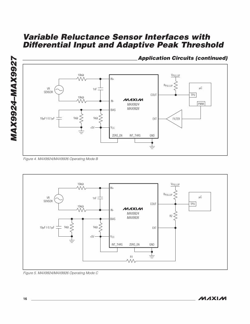
Figure 4. MAX9924/MAX9926 Operating Mode B
IN+
IN-
BIAS
VCC
ZERO_ENINT_THRS
R1
GND
COUT
EXT
TPU
μC
VPULLUP
RPULLUP
R2
1nF
10kΩ
10kΩ
VRSENSOR
+5V
1kΩ1kΩ10μF || 0.1μF
MAX9924MAX9926
Figure 5. MAX9924/MAX9926 Operating Mode C
MA
X9
92
4–M
AX
99
27
Variable Reluctance Sensor Interfaces withDifferential Input and Adaptive Peak Threshold
______________________________________________________________________________________ 17
Application Circuits (continued)
IN-
IN+
BIAS
VCC
ZERO_EN INT_THRS GND
COUT
OUT
EXT
TPU
μC
VPULLUP
RPULLUP1nF
10kΩ
10kΩ
VRSENSOR
+5V
1kΩ1kΩ10μF || 0.1μF
MAX9925MAX9927
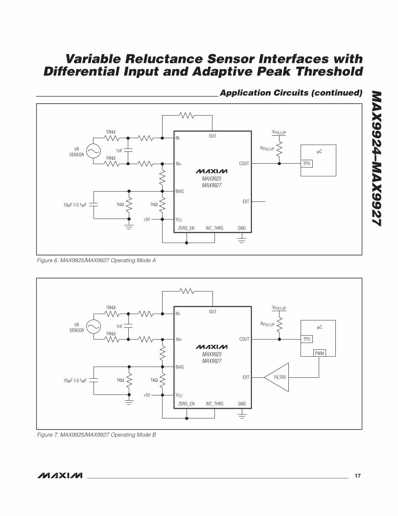
Figure 6. MAX9925/MAX9927 Operating Mode A
IN-
IN+
BIAS
VCC
ZERO_EN INT_THRS GND
COUT
OUT
EXT
TPU
μC
VPULLUP
RPULLUP1nF
10kΩ
10kΩ
VRSENSOR
+5V
1kΩ1kΩ10μF || 0.1μF
MAX9925MAX9927
PWM
FILTER
Figure 7. MAX9925/MAX9927 Operating Mode B
MA
X9
92
4–M
AX
99
27
Variable Reluctance Sensor Interfaces withDifferential Input and Adaptive Peak Threshold
18 ______________________________________________________________________________________
Application Circuits (continued)
IN-
IN+
BIAS
VCC
ZERO_ENINT_THRS
R1
GND
COUT
OUT
EXT
TPU
μC
VPULLUP
RPULLUP
R2
+5V
1kΩ1kΩ10μF || 0.1μF
MAX9925
1nF
10kΩ
10kΩ
VRSENSOR
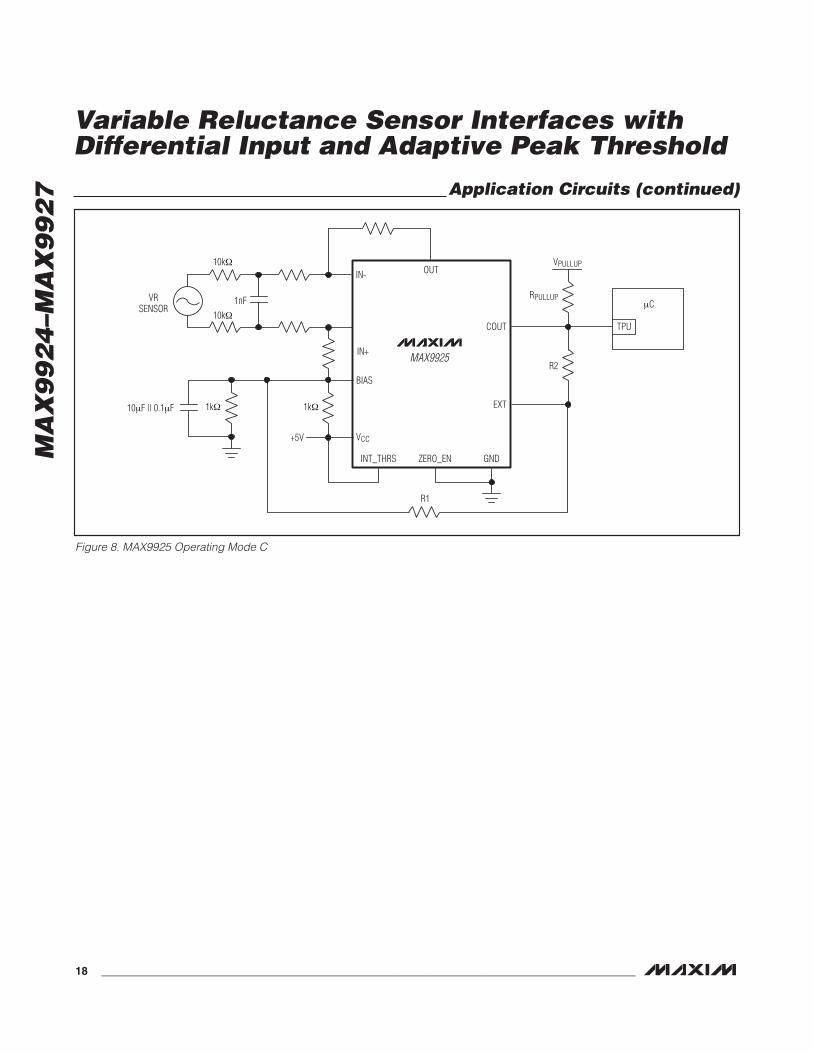
Figure 8. MAX9925 Operating Mode C
MA
X9
92
4–M
AX
99
27
Variable Reluctance Sensor Interfaces withDifferential Input and Adaptive Peak Threshold
______________________________________________________________________________________ 19
MAX9924
100kΩ
100kΩ
10kΩ
100kΩ
VCC
VCC
4.5V TO 5.5V
VCC
RPULLUP
VPULLUP
MODELOGIC
INT_THRS GND
EXT
IN-
100kΩ
VCC
IN+
BIAS
*THE MAX9924 ISCONFIGURED IN MODE A2.
OP AMP
COMPARATOR
30%
BUFFER
BANDGAPREFERENCE
VOLTAGE = 2 x VBG
VMINTHRESHOLD
85msWATCHDOG
μC
PEAKDETECTOR
MODELOGIC
COUTTPU
ZERO_EN
VR SENSOR
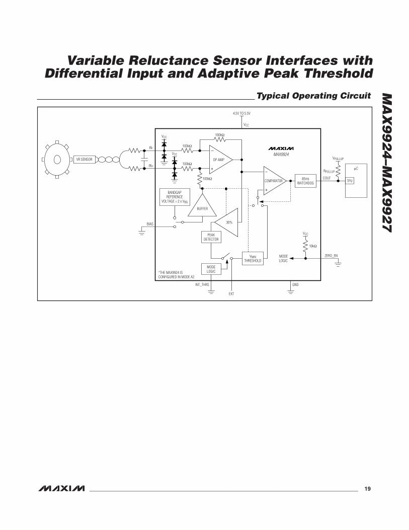
Typical Operating Circuit
MA
X9
92
4–M
AX
99
27
Variable Reluctance Sensor Interfaces withDifferential Input and Adaptive Peak Threshold
20 ______________________________________________________________________________________
Pin Configurations
16
15
14
13
12
11
10
9
1
2
3
4
5
6
7
8
IN_THRS1 IN1+
IN1-
VCC
ZERO_EN
DIRN
GND
IN2-
IN2+
TOP VIEW
MAX9926
QSOP
EXT1
BIAS1
BIAS2
COUT1
COUT2
EXT2
INT_THRS2
+16
15
14
13
12
11
10
9
1
2
3
4
5
6
7
8
IN_THRS1 IN1+
IN1-
VCC
OUT1
OUT2
GND
IN2-
IN2+
MAX9927
QSOP
EXT1
BIAS1
BIAS2
COUT1
COUT2
EXT2
INT_THRS2
+
1 +
2
3
4
5
10
9
8
7
6
VCC
INT_THRS
EXT
COUTBIAS
N.C.
IN-
IN+
MAX9924
μMAX
TOP VIEW
ZERO_ENGND
1
2
3
4
5
10
9
8
7
6
VCC
INT_THRS
EXT
COUTBIAS
OUT
IN-
IN+
MAX9925
μMAX
ZERO_ENGND
+
Chip InformationPROCESS: BiCMOS
Selector Guide
PART AMPLIFIER GAIN
MAX9924UAUB 1 x Differential 1V/V
MAX9925AUB 1 x Operational Externally Set
MAX9926UAEE 2 x Differential 1V/V
MAX9927AEE 2 x Operational Externally Set
MA
X9
92
4–M
AX
99
27
10LU
MA
X.E
PS
α
α
Variable Reluctance Sensor Interfaces withDifferential Input and Adaptive Peak Threshold
______________________________________________________________________________________ 21
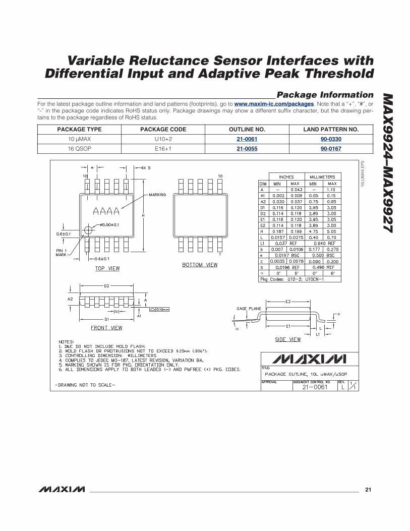
PACKAGE TYPE PACKAGE CODE OUTLINE NO. LAND PATTERN NO.
10 µMAX U10+2 21-0061 90-0330
16 QSOP E16+1 21-0055 90-0167
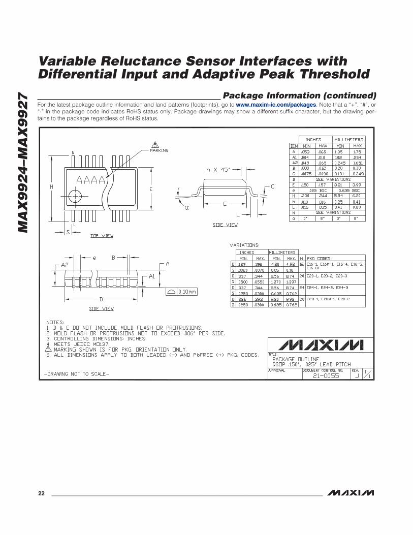
Package InformationFor the latest package outline information and land patterns (footprints), go to www.maxim-ic.com/packages. Note that a “+”, “#”, or“-” in the package code indicates RoHS status only. Package drawings may show a different suffix character, but the drawing per-tains to the package regardless of RoHS status.
MA
X9
92
4–M
AX
99
27
Variable Reluctance Sensor Interfaces withDifferential Input and Adaptive Peak Threshold
22 ______________________________________________________________________________________
Package Information (continued)For the latest package outline information and land patterns (footprints), go to www.maxim-ic.com/packages. Note that a “+”, “#”, or“-” in the package code indicates RoHS status only. Package drawings may show a different suffix character, but the drawing per-tains to the package regardless of RoHS status.
MA
X9
92
4–M
AX
99
27
Variable Reluctance Sensor Interfaces withDifferential Input and Adaptive Peak Threshold
Maxim cannot assume responsibility for use of any circuitry other than circuitry entirely embodied in a Maxim product. No circuit patent licenses areimplied. Maxim reserves the right to change the circuitry and specifications without notice at any time.
Maxim Integrated Products, 120 San Gabriel Drive, Sunnyvale, CA 94086 408-737-7600 ____________________ 23
.cnI ,stcudorP detargetnI mixaM fo kramedart deretsiger a si mixaM stcudorP detargetnI mixaM 2102©
Revision History
REVISIONNUMBER
REVISIONDATE
DESCRIPTIONPAGES
CHANGED
0 10/08 Initial release —
1 2/09Removed future product references for the MAX9926 and MAX9927, updated ECtable
1–4
2 3/09 Corrected various errors
3/11 Updated Figures 6, 7, and 8
3/12 Added automotive qualifies parts
2, 3, 4, 6, 13
3 17, 18
4 1