
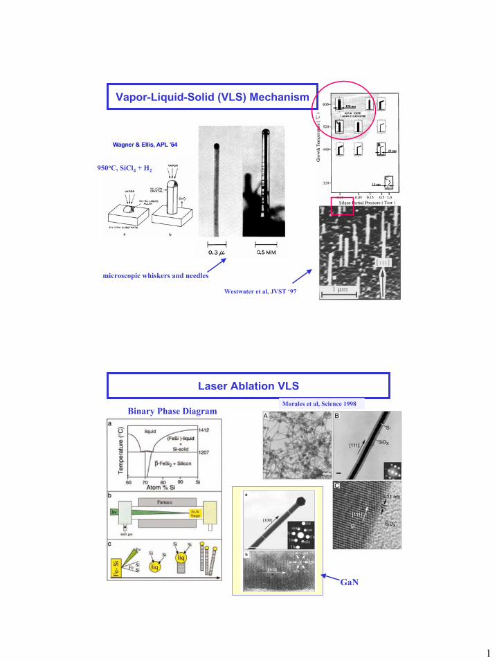
Vapor-Liquid-Solid (VLS) Mechanism
27
1 Vapor-Liquid-Solid (VLS) Mechanism microscopic whiskers and needles 950 o C, SiCl 4 + H 2 Westwater et al, JVST ‘97 Laser Ablation VLS Binary Phase Diagram Morales et al, Science 1998 GaN
Transcript of Vapor-Liquid-Solid (VLS) Mechanism
1
Vapor-Liquid-Solid (VLS) Mechanism
microscopic whiskers and needles
950oC, SiCl4 + H2
Westwater et al, JVST ‘97
Laser Ablation VLS
Binary Phase DiagramMorales et al, Science 1998
GaN
2
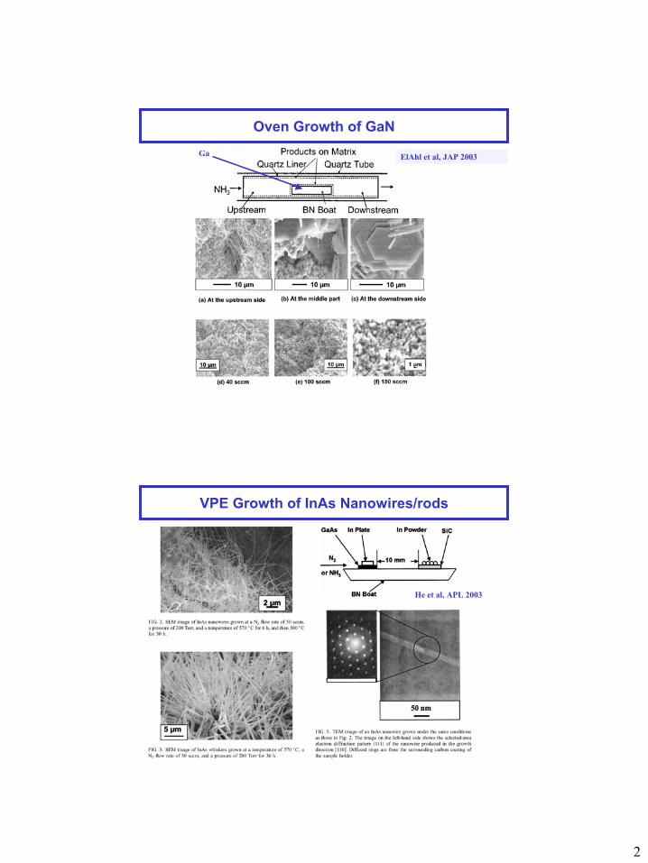
Oven Growth of GaN
ElAhl et al, JAP 2003Ga
VPE Growth of InAs Nanowires/rods
He et al, APL 2003
3
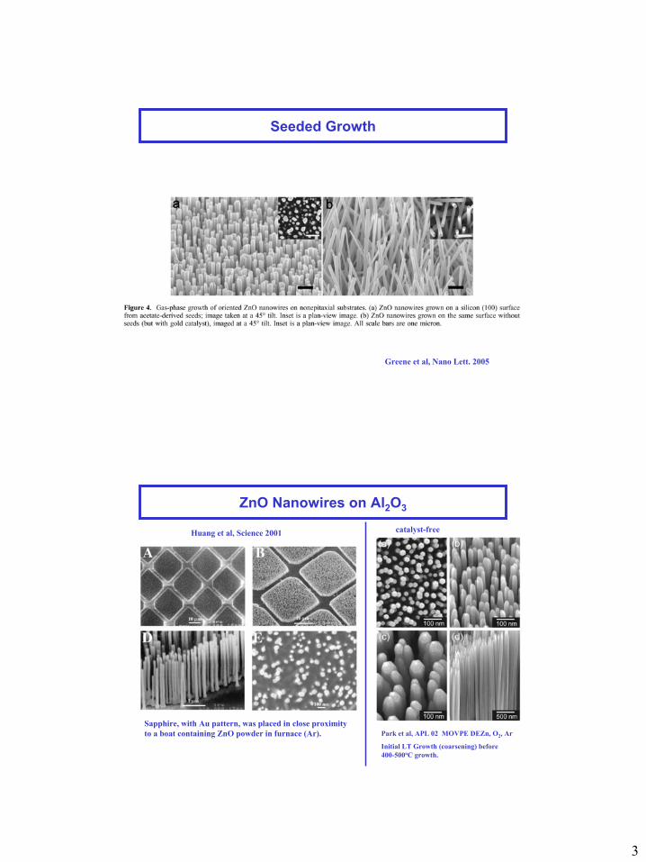
Seeded Growth
Greene et al, Nano Lett. 2005
ZnO Nanowires on Al2O3
Huang et al, Science 2001
Sapphire, with Au pattern, was placed in close proximity to a boat containing ZnO powder in furnace (Ar). Park et al, APL 02 MOVPE DEZn, O2, Ar
Initial LT Growth (coarsening) before 400-500oC growth.
catalyst-free
4
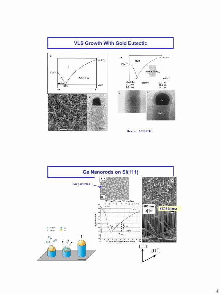
VLS Growth With Gold Eutectic
Hu et al, ACR 1999
Ge Nanorods on Si(111)
Au particles
SEM images
]111[]111[

5
Nanowires On Step EdgesLin et al, APL 2001
Strain Anisotropy
Au particlesChen et al, JAP 2002
6
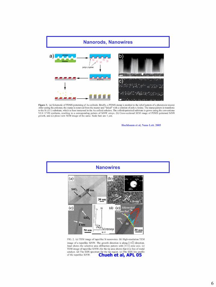
Nanorods, Nanowires
Hochbaum et al, Nano Lett. 2005
Nanowires
7
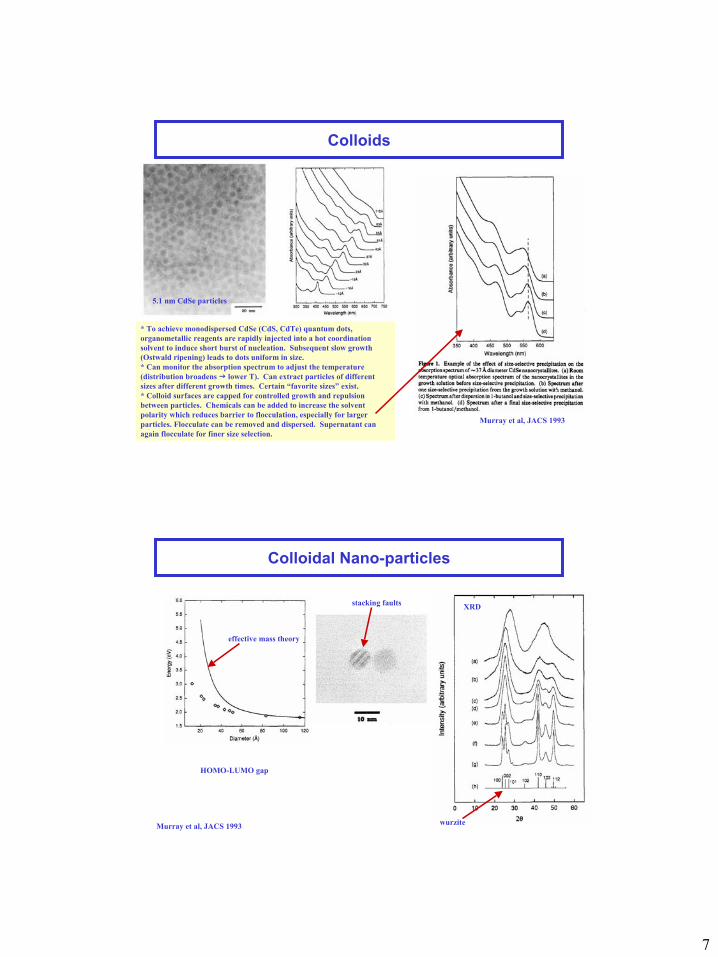
Colloids
Murray et al, JACS 1993
* To achieve monodispersed CdSe (CdS, CdTe) quantum dots, organometallic reagents are rapidly injected into a hot coordination solvent to induce short burst of nucleation. Subsequent slow growth (Ostwald ripening) leads to dots uniform in size. * Can monitor the absorption spectrum to adjust the temperature (distribution broadens lower T). Can extract particles of different sizes after different growth times. Certain “favorite sizes” exist.* Colloid surfaces are capped for controlled growth and repulsion between particles. Chemicals can be added to increase the solvent polarity which reduces barrier to flocculation, especially for larger particles. Flocculate can be removed and dispersed. Supernatant can again flocculate for finer size selection.
5.1 nm CdSe particles
Colloidal Nano-particles
Murray et al, JACS 1993
HOMO-LUMO gap
XRDstacking faults
wurzite
effective mass theory
8
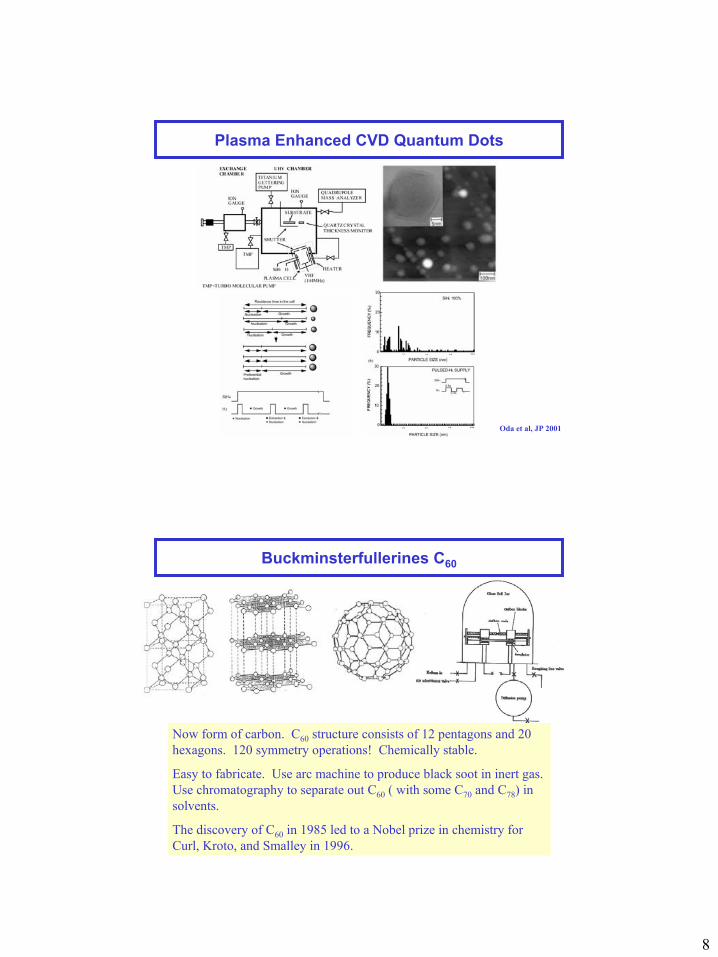
Plasma Enhanced CVD Quantum Dots
Oda et al, JP 2001
Buckminsterfullerines C60
Now form of carbon. C60 structure consists of 12 pentagons and 20 hexagons. 120 symmetry operations! Chemically stable.
Easy to fabricate. Use arc machine to produce black soot in inert gas. Use chromatography to separate out C60 ( with some C70 and C78) in solvents.
The discovery of C60 in 1985 led to a Nobel prize in chemistry for Curl, Kroto, and Smalley in 1996.
9
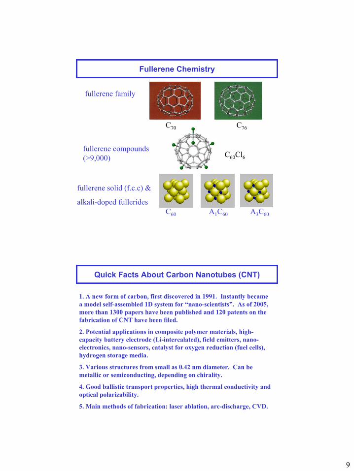
Fullerene Chemistry
fullerene family
C70 C76
fullerene compounds (>9,000) C60Cl6
fullerene solid (f.c.c) &
alkali-doped fulleridesC60 A1C60 A3C60
Quick Facts About Carbon Nanotubes (CNT)
1. A new form of carbon, first discovered in 1991. Instantly became a model self-assembled 1D system for “nano-scientists”. As of 2005, more than 1300 papers have been published and 120 patents on thefabrication of CNT have been filed.
2. Potential applications in composite polymer materials, high-capacity battery electrode (Li-intercalated), field emitters, nano-electronics, nano-sensors, catalyst for oxygen reduction (fuel cells), hydrogen storage media.
3. Various structures from small as 0.42 nm diameter. Can be metallic or semiconducting, depending on chirality.
4. Good ballistic transport properties, high thermal conductivity and optical polarizability.
5. Main methods of fabrication: laser ablation, arc-discharge, CVD.
10
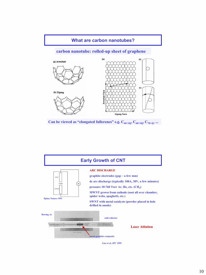
What are carbon nanotubes?
Can be viewed as “elongated fullerenes” e.g. C60+10j, C60+18j, C78+4j, ...
carbon nanotube: rolled-up sheet of graphene
Early Growth of CNT
ARC DISCHARGE
graphite electrodes (gap ~ a few mm)
dc arc discharge (typically 100A, 30V, a few minutes)
pressure 10-760 Torr Ar, He, etc. (CH4)
MWNT grown from cathode (soot all over chamber, spider webs, spaghetti, etc.)
SWNT with metal catalysts (powder placed in hole drilled in anode)
Laser Ablation
metal-graphite composite
flowing Arcold collector
Guo et al, JPC 1995
Iijima Nature 1991
11
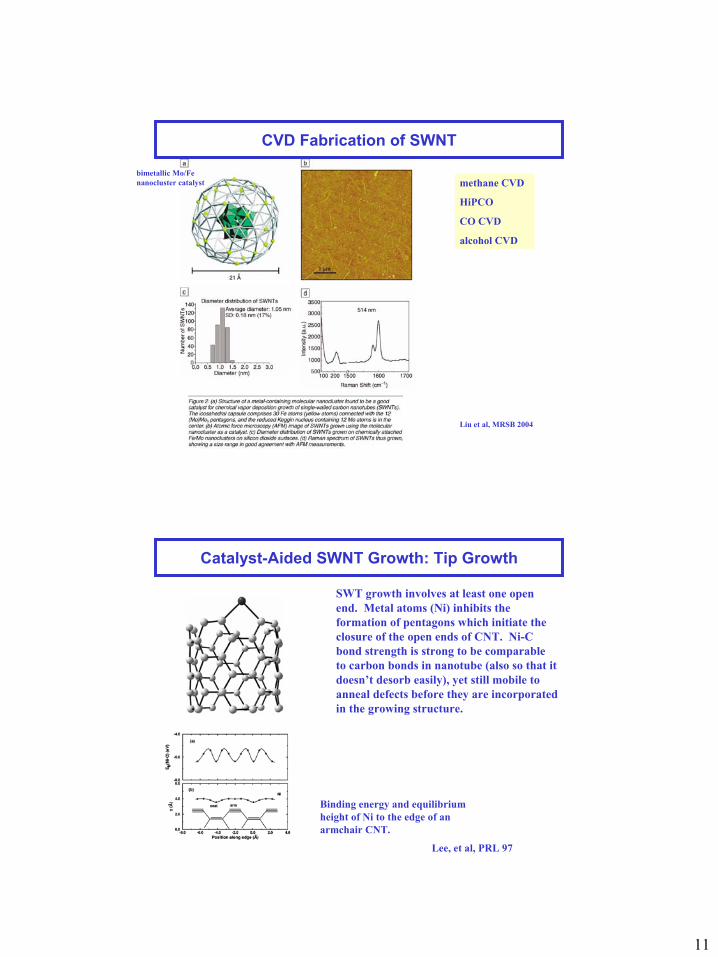
CVD Fabrication of SWNT
Liu et al, MRSB 2004
methane CVD
HiPCO
CO CVD
alcohol CVD
bimetallic Mo/Fe nanocluster catalyst
Catalyst-Aided SWNT Growth: Tip Growth
SWT growth involves at least one open end. Metal atoms (Ni) inhibits the formation of pentagons which initiate the closure of the open ends of CNT. Ni-C bond strength is strong to be comparable to carbon bonds in nanotube (also so that it doesn’t desorb easily), yet still mobile to anneal defects before they are incorporated in the growing structure.
Lee, et al, PRL 97
Binding energy and equilibrium height of Ni to the edge of an armchair CNT.
12
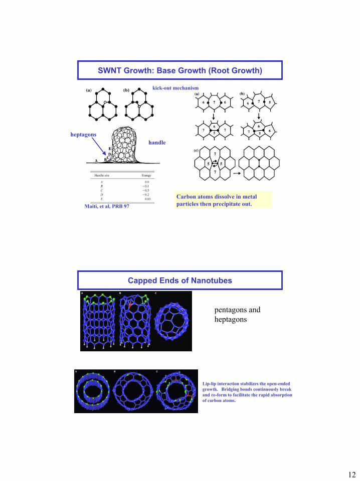
SWNT Growth: Base Growth (Root Growth)
handle
Maiti, et al, PRB 97
kick-out mechanism
Carbon atoms dissolve in metal particles then precipitate out.
heptagons
Capped Ends of Nanotubes
pentagons and heptagons
Lip-lip interaction stabilizes the open-ended growth. Bridging bonds continuously break and re-form to facilitate the rapid absorption of carbon atoms.

13
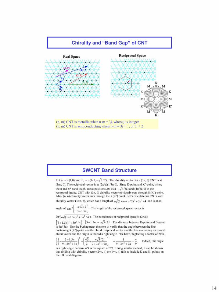
Chirality Of CNT
graphene
dC-C = 0.142 nm
Ch = na1 + ma2 (chirality vec.)
radius = Ch/2π
zig-zag
(n, 0)
θ = 0oarmchair
(n, n)
θ = 30ochiral (no mirror symm.)
(n, m)
Electronic Structure of CNTs
bonds and bands of various forms of carbon:Four valence electrons per atom.
Common bonding configuration sp3 and sp2.
graphene sheet
Avouris, CP 2002
14
Chirality and “Band Gap” of CNT
(n, m) CNT is metallic when n-m = 3j, where j is integer(n, m) CNT is semiconducting when n-m = 3j + 1, or 3j + 2
SWCNT Band Structure

15
Electronic Structure & Optical Properties
s
van Hove singularities
Jorio et al, MRSB 2004
free electrons
h
)(2 0EEmk
−=
)(2 0EEmdEdk−
=h
dkLdN
=π
Optical Determination of CNT Chirality
“Kataura” plot
Filho et al, NT 2003
selection rules
S: semiconducting
M: metallic
16
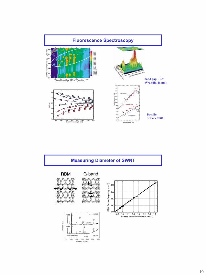
Fluorescence Spectroscopy
Bachilo, Science 2002
band gap ~ 0.9 eV/d (dia. in nm)
Measuring Diameter of SWNT
17
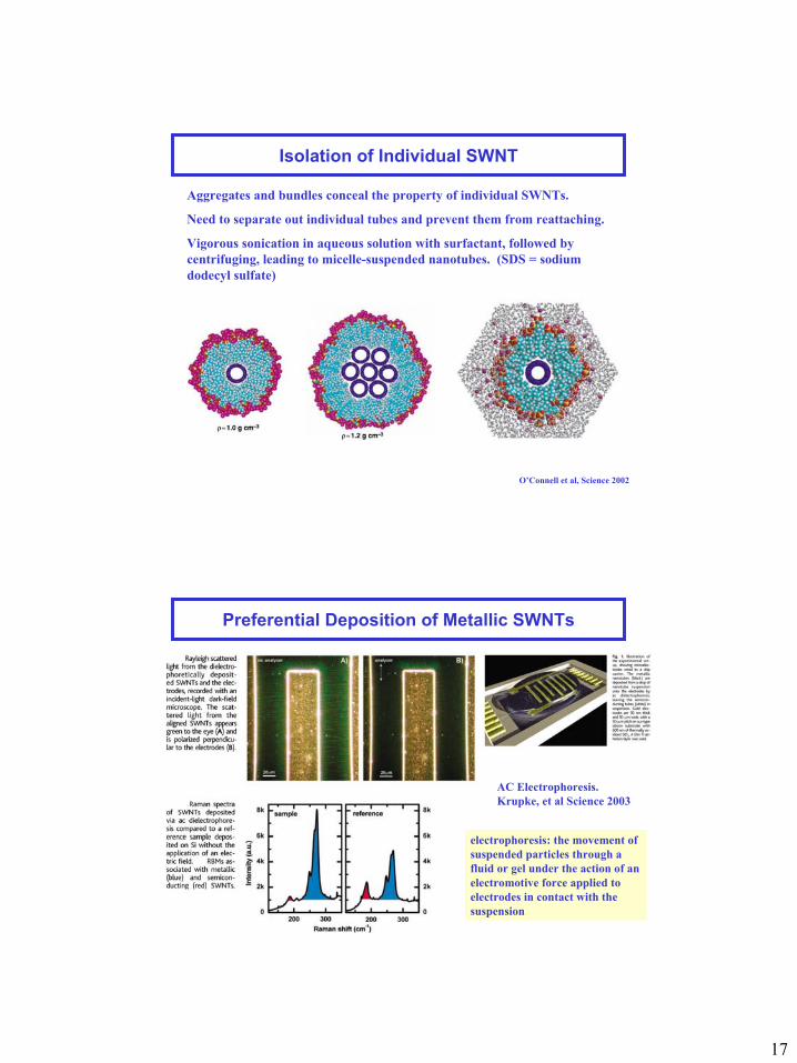
Isolation of Individual SWNT
Aggregates and bundles conceal the property of individual SWNTs.
Need to separate out individual tubes and prevent them from reattaching.
Vigorous sonication in aqueous solution with surfactant, followed by centrifuging, leading to micelle-suspended nanotubes. (SDS = sodium dodecyl sulfate)
O’Connell et al, Science 2002
Preferential Deposition of Metallic SWNTs
AC Electrophoresis. Krupke, et al Science 2003
electrophoresis: the movement of suspended particles through a fluid or gel under the action of an electromotive force applied to electrodes in contact with the suspension
18
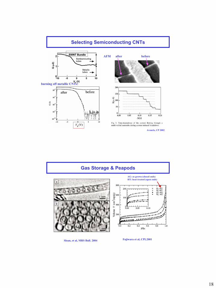
Selecting Semiconducting CNTs
AFM after before
burning off metallic CNTs!
Avouris, CP 2002
Gas Storage & Peapods
Sloan, et al, MRS Bull. 2004 Fujiwara et al, CPL2001
AG: as grown (closed ends) HT: heat treated (open ends)
19
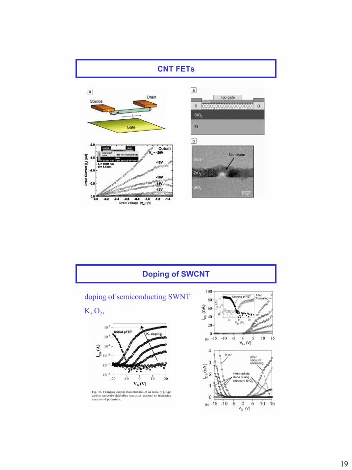
CNT FETs
Doping of SWCNT
doping of semiconducting SWNT
K, O2,
20
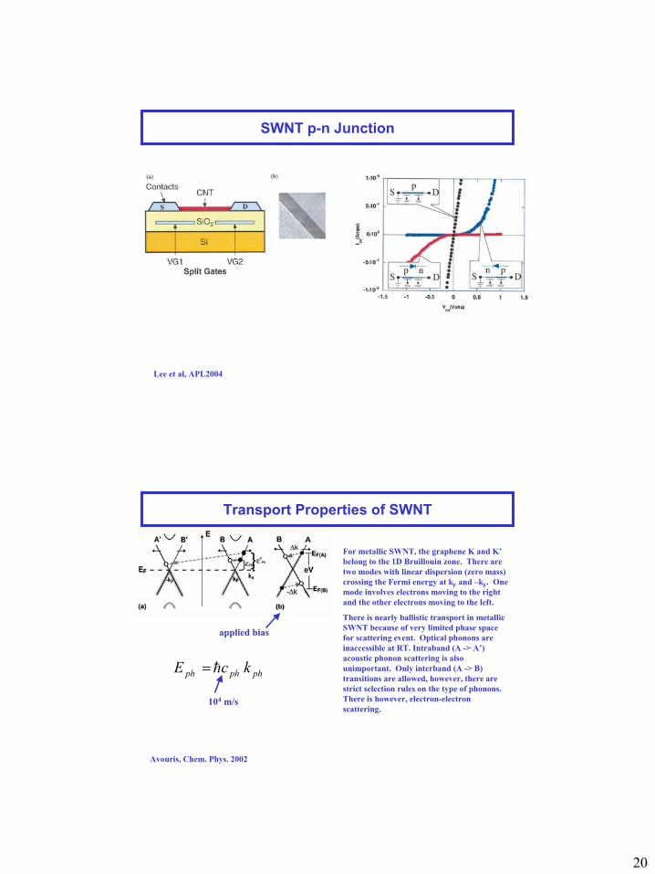
SWNT p-n Junction
Lee et al, APL2004
Transport Properties of SWNT
For metallic SWNT, the graphene K and K’ belong to the 1D Bruillouin zone. There are two modes with linear dispersion (zero mass) crossing the Fermi energy at kF and –kF. One mode involves electrons moving to the right and the other electrons moving to the left.
There is nearly ballistic transport in metallic SWNT because of very limited phase space for scattering event. Optical phonons are inaccessible at RT. Intraband (A -> A’) acoustic phonon scattering is also unimportant. Only interband (A -> B) transitions are allowed, however, there are strict selection rules on the type of phonons. There is however, electron-electron scattering.
applied bias
phphph kcE h=
104 m/s
Avouris, Chem. Phys. 2002
21
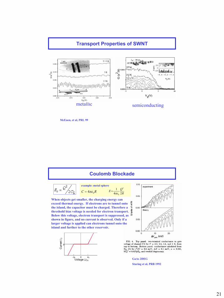
Transport Properties of SWNT
semiconductingmetallic
McEuen, et al, PRL 99
Coulomb Blockade
When objects get smaller, the charging energy can exceed thermal energy. If electrons are to tunnel onto the island, the capacitor must be charged. Therefore a threshold bias voltage is needed for electron transport. Below this voltage, electron transport is suppressed, as shown in figure, and no current is observed. Only if a larger voltage is applied can electrons tunnel onto the island and further to the other reservoir.
GaAs 2DEG
Staring et al, PRB 1992
example: metal sphere
RC 04πε= RQE24
1 2
0πε=
22
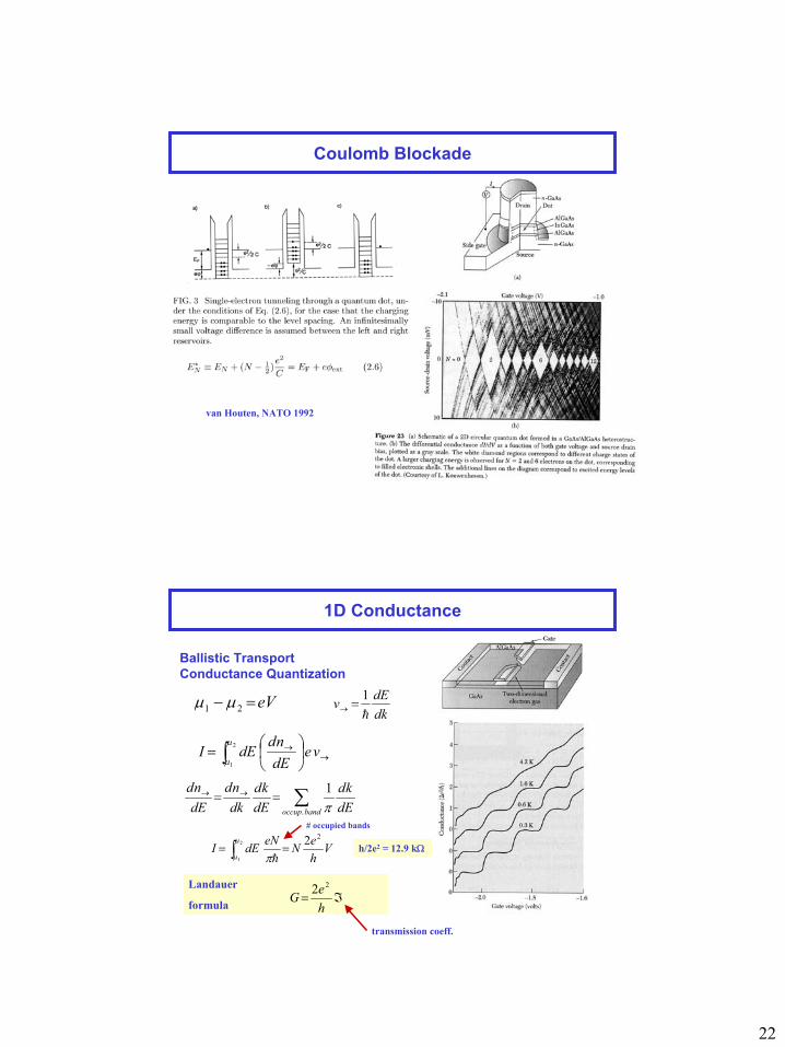
Coulomb Blockade
van Houten, NATO 1992
1D Conductance
Landauer
formula
Ballistic TransportConductance Quantization
eV=− 21 µµ
→→
= ∫ vedEnd
dEI 2
1
µ
µ
dkdEv
h
1=→
dEkd
dEkd
dknd
dEnd
bandoccup π1
.∑== →→
VheNeNdEI
222
1
== ∫ hπµ
µ
ℑ=heG
22
transmission coeff.
# occupied bands
h/2e2 = 12.9 kΩ
23
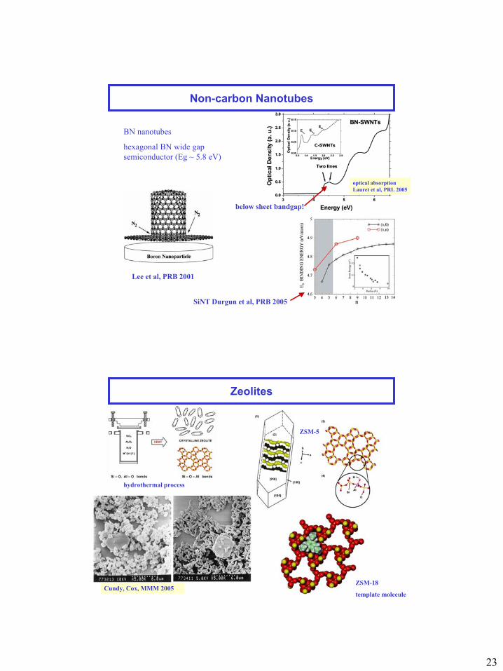
Non-carbon Nanotubes
BN nanotubes
hexagonal BN wide gap semiconductor (Eg ~ 5.8 eV)
Lee et al, PRB 2001
below sheet bandgap!
optical absorption Lauret et al, PRL 2005
SiNT Durgun et al, PRB 2005
Zeolites
ZSM-5
ZSM-18
template moleculeCundy, Cox, MMM 2005
hydrothermal process

24
Micro Self-Assembly
Clark et al, JACS 2001
Evaporation Induced Self Assembly (EISA)
Brinker et al, Adv. Mater. 1999
25
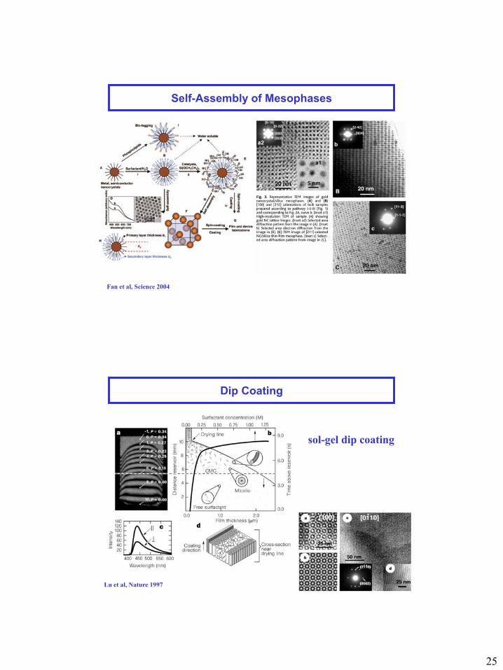
Self-Assembly of Mesophases
Fan et al, Science 2004
Dip Coating
Lu et al, Nature 1997
sol-gel dip coating
26
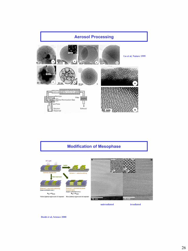
Aerosol Processing
Lu et al, Nature 1999
Modification of Mesophase
unirradiated irradiated
Doshi et al, Science 2000
27
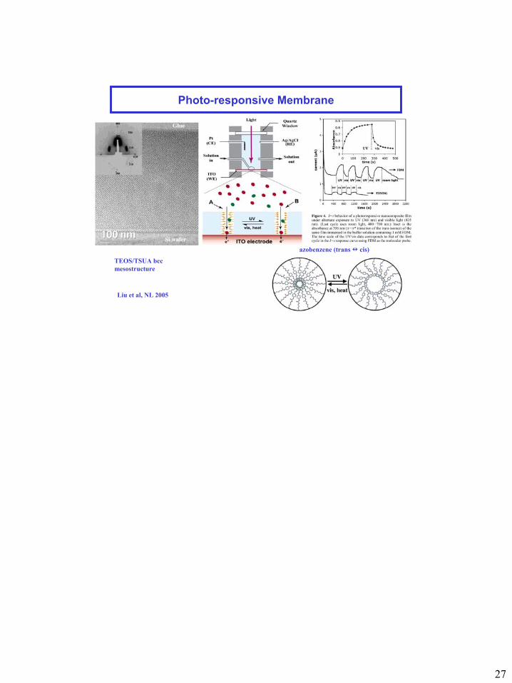
Photo-responsive Membrane
azobenzene (trans cis)
TEOS/TSUA bcc mesostructure
Liu et al, NL 2005


![Directional growth of metallic and polymeric nanowiresutol.okstate.edu/sites/default/files/publications/pubs/147_paper-145.pdf · metals [6, 9]. The vapor–liquid–solid (VLS) technique](https://static.fdocuments.in/doc/165x107/5e046a5a874da4285344687f/directional-growth-of-metallic-and-polymeric-metals-6-9-the-vaporaliquidasolid.jpg)
