VALUATION KIT USER S GUIDE - Silicon Labs · PDF filePinout for J2 Pin 1 SPI Bus—SCLK...
7
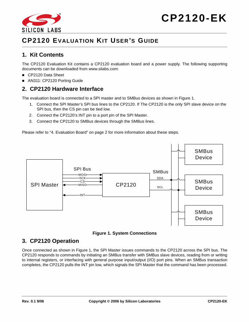
Rev. 0.1 9/06 Copyright © 2006 by Silicon Laboratories CP2120-EK CP2120-EK CP2120 E VALUATION K IT U SER ’ S G UIDE 1. Kit Contents The CP2120 Evaluation Kit contains a CP2120 evaluation board and a power supply. The following supporting documents can be downloaded from www.silabs.com: CP2120 Data Sheet AN311: CP2120 Porting Guide 2. CP2120 Hardware Interface The evaluation board is connected to a SPI master and to SMBus devices as shown in Figure 1. 1. Connect the SPI Master’s SPI bus lines to the CP2120. If The CP2120 is the only SPI slave device on the SPI bus, then the CS pin can be tied low. 2. Connect the CP2120’s INT pin to a port pin of the SPI Master. 3. Connect the CP2120 to SMBus devices through the SMBus lines. Please refer to "4. Evaluation Board" on page 2 for more information about these steps. Figure 1. System Connections 3. CP2120 Operation Once connected as shown in Figure 1, the SPI Master issues commands to the CP2120 across the SPI bus. The CP2120 responds to commands by initiating an SMBus transfer with SMBus slave devices, reading from or writing to internal registers, or interfacing with general purpose input/output (I/O) port pins. When an SMBus transaction completes, the CP2120 pulls the INT pin low, which signals the SPI Master that the command has been processed. SPI Master CP2120 SMBus Device SMBus Device SMBus Device SCK CS MISO MOSI INT SPI Bus SDA SCL SMBus
Transcript of VALUATION KIT USER S GUIDE - Silicon Labs · PDF filePinout for J2 Pin 1 SPI Bus—SCLK...
Rev. 0.1 9/06 Copyright © 2006 by Silicon Laboratories CP2120-EK
CP2120-EK
CP2120 EVALUATION KIT USER’S GUIDE
1. Kit Contents
The CP2120 Evaluation Kit contains a CP2120 evaluation board and a power supply. The following supportingdocuments can be downloaded from www.silabs.com:
CP2120 Data Sheet
AN311: CP2120 Porting Guide
2. CP2120 Hardware Interface
The evaluation board is connected to a SPI master and to SMBus devices as shown in Figure 1.
1. Connect the SPI Master’s SPI bus lines to the CP2120. If The CP2120 is the only SPI slave device on the SPI bus, then the CS pin can be tied low.
2. Connect the CP2120’s INT pin to a port pin of the SPI Master.
3. Connect the CP2120 to SMBus devices through the SMBus lines.
Please refer to "4. Evaluation Board" on page 2 for more information about these steps.
Figure 1. System Connections
3. CP2120 Operation
Once connected as shown in Figure 1, the SPI Master issues commands to the CP2120 across the SPI bus. TheCP2120 responds to commands by initiating an SMBus transfer with SMBus slave devices, reading from or writingto internal registers, or interfacing with general purpose input/output (I/O) port pins. When an SMBus transactioncompletes, the CP2120 pulls the INT pin low, which signals the SPI Master that the command has been processed.
SPI Master CP2120
SMBus Device
SMBus Device
SMBus Device
SCKCS
MISO
MOSI
INT
SPI Bus
SDA
SCL
SMBus

CP2120-EK
2 Rev. 0.1
4. Evaluation Board
The CP2120 evaluation board comes with a CP2120 device pre-installed for system evaluation and development.Numerous I/O connections are provided to facilitate prototyping using the evaluation board. Refer to Figure 2 forthe locations of the various I/O connectors.
J1 Power Connector
J2 SPI Master Interface
J3 SMBus Interface
J4 MISO-MOSI Connector
J6 SMBus SDA Pullup Connector
J7 SMBus SCL Pullup Connector
J9 LED Connector
J10 General Purpose I/O Interface
Figure 2. CP2120 Evaluation Board
D7 D0D1D2D3D4D5D6
POWER
J1
J9
J10
J3
J2
J7
J6
SILI
CO
N L
ABO
RAT
OR
IES
SA
-TB
51P
CB
J4

CP2120-EK
Rev. 0.1 3
4.1. J2—SPI Master InterfaceConnector J2 provides the SPI Master access to the CP2120 SPI, control, and reset lines. Table 1 shows thepinout of the J2 header.
4.2. J3—SMBus InterfaceConnector J3 provides the CP2120 access to the SMBus. Table 2 shows the pinout of the J3 header.
Note: All pins labeled SCL are tied together, and all pins labeled SDA are tied together. Multiple connections to SCL and SDAsignals are provided to allow multiple devices to connect to the evaluation board.
Table 1. Pinout for J2
Pin 1 SPI Bus—SCLK
Pin 2 SPI Bus—MISO
Pin 3 SPI Bus—MOSI
Pin 4 SPI Bus—CS
Pin 5 INT
Pin 6 Not Used
Pin 7 RST
Pin 8 GND
Pin 9 Not Used
Pin 10 Not Used
Table 2. Pinout for J3
Pin 1 SMBus—SCL
Pin 2 SMBus—SDA
Pin 3 SMBus—SCL
Pin 4 SMBus—SDA
Pin 5 SMBus—SCL
Pin 6 SMBus—SDA
Pin 7 SMBus—SCL
Pin 8 SMBus—SDA
Pin 9 GND
Pin 10 GND

CP2120-EK
4 Rev. 0.1
4.3. J4—SPI MISO/MOSI ConnectorSome SPI master systems tie together the MISO and MOSI SPI data lines. The CP2120 evaluation board allowsdevelopers to connect these two signals through a resistor by placing a header on J4.
Note: When operating the SPI bus with a header on J4, only drive the MOSI pin whenever data is being transmitted to theCP2120. When the SPI bus is idle, or when the CP2120 is transmitting data, the SPI master must set its MOSI pin intoan open-drain state to avoid port pin contention.
4.4. J6 and J7—SMBus Pullup ConnectorsConnectors J6 and J7 give developers the option of adding pullup resistors to the SMBus’s SDA and SCL lines.Removing shorting blocks from these headers disconnects the pullups from the SMBus lines.
Note: The SMBus lines need pullups to VDD in order to function properly. If the headers are removed from J6 and J7, remem-
ber to add pullups to VDD elsewhere on the SMBus.
4.5. J9—LED ConnectorConnector J9 allows the CP2120’s General Purpose I/O pins to be connected to the array of LEDs on theevaluation board. Once a header has been placed connecting a pin on the side closest to the CP2120 to itscorresponding pin on the side of the jumper closest to the LEDs. To use one of the LEDs, place a shorting block onthe J9 pin closest to the LED, connecting the corresponding J9 pin on the side of the connector closer to theCP2120. See Figure 3 for an example of this connection. Writing a 0 to the connected general purpose I/O pin willturn on the LED, and writing a 1 to that pin will turn off the LED.
Figure 3. Controlling the LEDs
Shorting Block placed on GPIO1, with GPIO1
configured to be Digital Output and set to ‘0’
GP
IO0
GP
IO1
GP
IO2
GP
IO3
GP
IO4
GP
IO5
GP
IO6
GP
IO7
CP2120
To Control an LED using the CP2120:� Add Shorting Block to LED’s
corresponding port pin� Configure port pin to Digital Output� To turn on LED: Set port pin to ‘0’� To turn off LED: Set port pin to ‘1’
J9
CP2120-EK
Rev. 0.1 5
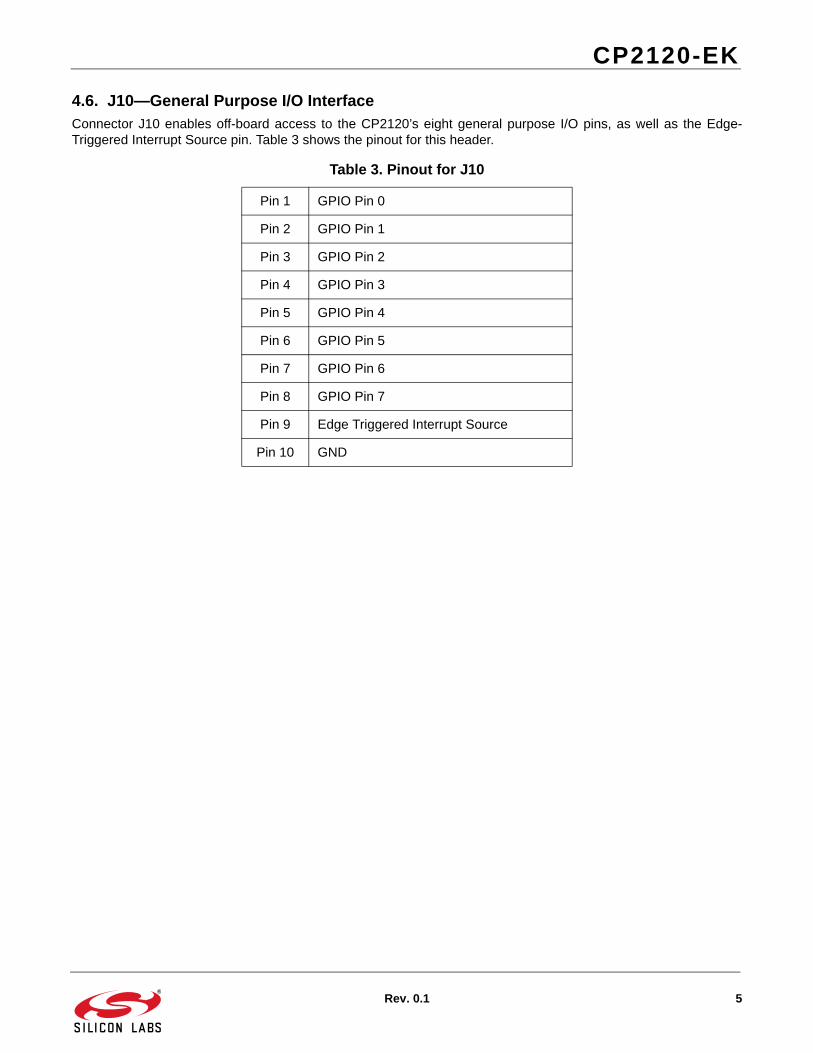
4.6. J10—General Purpose I/O InterfaceConnector J10 enables off-board access to the CP2120’s eight general purpose I/O pins, as well as the Edge-Triggered Interrupt Source pin. Table 3 shows the pinout for this header.
Table 3. Pinout for J10
Pin 1 GPIO Pin 0
Pin 2 GPIO Pin 1
Pin 3 GPIO Pin 2
Pin 4 GPIO Pin 3
Pin 5 GPIO Pin 4
Pin 6 GPIO Pin 5
Pin 7 GPIO Pin 6
Pin 8 GPIO Pin 7
Pin 9 Edge Triggered Interrupt Source
Pin 10 GND

CP2120-EK
6 Rev. 0.1
5. Schematic

http://www.silabs.com
Silicon Laboratories Inc.400 West Cesar ChavezAustin, TX 78701USA
Simplicity Studio
One-click access to MCU and wireless tools, documentation, software, source code libraries & more. Available for Windows, Mac and Linux!
IoT Portfoliowww.silabs.com/IoT
SW/HWwww.silabs.com/simplicity
Qualitywww.silabs.com/quality
Support and Communitycommunity.silabs.com
DisclaimerSilicon Labs intends to provide customers with the latest, accurate, and in-depth documentation of all peripherals and modules available for system and software implementers using or intending to use the Silicon Labs products. Characterization data, available modules and peripherals, memory sizes and memory addresses refer to each specific device, and "Typical" parameters provided can and do vary in different applications. Application examples described herein are for illustrative purposes only. Silicon Labs reserves the right to make changes without further notice and limitation to product information, specifications, and descriptions herein, and does not give warranties as to the accuracy or completeness of the included information. Silicon Labs shall have no liability for the consequences of use of the information supplied herein. This document does not imply or express copyright licenses granted hereunder to design or fabricate any integrated circuits. The products are not designed or authorized to be used within any Life Support System without the specific written consent of Silicon Labs. A "Life Support System" is any product or system intended to support or sustain life and/or health, which, if it fails, can be reasonably expected to result in significant personal injury or death. Silicon Labs products are not designed or authorized for military applications. Silicon Labs products shall under no circumstances be used in weapons of mass destruction including (but not limited to) nuclear, biological or chemical weapons, or missiles capable of delivering such weapons.
Trademark InformationSilicon Laboratories Inc.® , Silicon Laboratories®, Silicon Labs®, SiLabs® and the Silicon Labs logo®, Bluegiga®, Bluegiga Logo®, Clockbuilder®, CMEMS®, DSPLL®, EFM®, EFM32®, EFR, Ember®, Energy Micro, Energy Micro logo and combinations thereof, "the world’s most energy friendly microcontrollers", Ember®, EZLink®, EZRadio®, EZRadioPRO®, Gecko®, ISOmodem®, Precision32®, ProSLIC®, Simplicity Studio®, SiPHY®, Telegesis, the Telegesis Logo®, USBXpress® and others are trademarks or registered trademarks of Silicon Labs. ARM, CORTEX, Cortex-M3 and THUMB are trademarks or registered trademarks of ARM Holdings. Keil is a registered trademark of ARM Limited. All other products or brand names mentioned herein are trademarks of their respective holders.