Vacuum Tube Design - americanradiohistory.com · a course on vacuum-tube design given by RCA...
267
VACUUM TUBE DESIGN
Transcript of Vacuum Tube Design - americanradiohistory.com · a course on vacuum-tube design given by RCA...
VACUUM TUBEDESIGN

Vacuum Tube Design
RCA Manufacturing Company, Inc.Harrison, New Jersey

Privately issued by RCA Manufacturing Co., Inc.
for use of its employees and for restricted
distribution.
Photolithographed in U.S.A.
PREFACE
The material comprising the twenty-six lec-tures contained in this book formed the basis ofa course on vacuum-tube design given by RCA engi-neers for company employees during the Winter of1937 and the Spring of 1938. The lectures wereintended to provide a review of the basic prin-ciples underlying the design and manufacture ofvacuum tubes. They appear in the order in which
they were presented and ina few instances includenew material added at time of publication.
Each lecturer has treated his subject accord-ing to his own viewpoint. In general, the treat-ment is non-mathematical. Numerous formulas andcharts of particular interest tothe design engi-neer have been included.
Throughout the book, numerous references to
sources of information have been given. Refer-
ences to published material list the publication;
those to unpublished material are keyed. The
keyed sources are available toauthorized personsfor reference purposes in our Library.
The Editors
Harrison, New JerseyDecember, 1940
CONTENTS
Lecture 1 FILAMENTS AND CATHODES - Part I E. A. Lederer
Lecture 2 FILAMENTS AND CATHODES - Part II E. A. Lederer 11
Lecture 3 HEATERS AND HEATER -CATHODEINSULATION G. R. Shaw and L. R. Shardlow 24
Lecture 4 PHOTOELECTRIC AND SECONDARY EMISSION L. B. Headrick 34
Lecture 5 LUMINESCENT MATERIALS H. W. Kaufmann 51
Lecture 6 CONTACT POTENTIAL, PUMPS, AND GETTERS E. A. Lederer 58
Lecture 7 METALLURGICAL PRINCIPLES S. Umbreit 73
Lecture 8 METALS FOR VACUUM -TUBE CONSTRUCTION S. Umbreit 82
Lecture 9 GLASS AND ITS PROPERTIES G. R. Shaw and C. A. Jacoby 91
Lecture 10 CONSTRUCTION TRENDS IN RADIO TUBES N. R. Smith 103
Lectures II, 12, 13, and 14 SPACE-CURRENT FLOW INVACUUM-TUBE STRUCTURES B. J. Thompson 115
Lecture 15 ELECTRON OPTICS -- Part IDETERMINATION OF ELECTRON
TRAJECTORIES V K. Zworykin and G. A. Morton 124
Lecture 16 ELECTRON OPTICS -- Part IIELECTRON -OPTICAL SYSTEMS WITH CYLINDRI-
CALLY SYMMETRICAL FIELD -PRODUCINGELEMENTS V. K. Zworykin and G. A. Morton 136
Lecture 17 ELECTRON OPTICS -- Part IIIABBERATIONS IN ELECTRON
OPTICS G. A. Morton and E. G. Ramberg 153
Lecture 18 RADIO RECEIVING TUBE COMPONENTSAND THEIR MANUFACTURE N. R. Smith 168
Lecture 19 ANALYSIS OF RECTIFIER OPERATION 0. H. Schade 174
Lecture 20 THE DESIGN OF AUDIO AMPLIFIER ANDPOWER OUTPUT TUBES S. W. Dodge 194
Lecture 21
Lecture 22
Lecture 23
CONTENTS (cont'd)
THE DESIGN OF RADIO -FREQUENCYAMPLIFIER TUBES
THE DESIGN OF DETECTORS AND CONVERTERS
THE DESIGN AND CONSTRUCTION OF
T. J. Henry
T. J. Henry
203
209
TRANSMITTING TUBES E. E. Spitzer 218
Lecture 24 THE DESIGN AND CONSTRUCTION OFCATHODE-RAY TUBES W. H. Painter 226
Lecture 25 ELECTRON BEAMS AND THEIR APPLI-CATION IN RADIO TUBES H. M. Wagner 234
Lecture 26 THE DESIGN AND PERFORMANCE OF RECTIFIERS A. P. Kauzmann 249
Page 25:
Page 114:
Page 117:
Page 180:
Page 183:
Page 185:
Page 190:
Page 243:
Page 249:
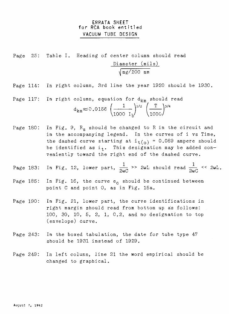
ERRATA SHEETfor RCA book entitled
VACUUM TUBE DESIGN
Table I. Heading of center column should read
Diameter (mils)
Jmg/200 mm
In right column, 3rd line the year 1920 should be 1930.
In right column, equation for dkm should read
dkm ;:0.01561 )1/2 ( T )3A
1000 Ib 1000
In Fig. 9, Rs should be changed to R in the circuit and
in the accompanying legend. In the curves of i vs Time,
the dashed curve starting at it(0) = 0.089 ampere shouldbe identified as it. This designation may be added con-
veniently toward the right end of the dashed curve.
In Fig. 12, lower part,1>>
2wC
12wL should read -.(7)c < <
In Fig. 16, the curve ec should be continued between
point C and point 0, as in Fig. 15a.
In Fig. 21, lower part, the curve identifications in
right margin should read from bottom up as follows:
100, 30, 10, 5, 2, 1, 0.2, and no designation to top
(envelope) curve.
In the boxed tabulation, the date for tube type 47
should be 1931 instead of 1929.
In left column, line 21 the word empirical should be
changed to graphical.
2wL.
August 7, 1942
Lecture I
FILAMENTS AND CATHODES -- Part I
E. A. Lederer
A. THERMIONIC EMISSION
1. Introduction
Electrons can be dislodged from matter by theaction of incident light, by bombardment withelectrons, by bombardment with positive ions, bymetastable atoms, by the action of heat, or byapplying intense fields. In the following weshR11 confine our interest only to the action ofheat, commonly termed the field of thermionics.
The name implies that electron emission soobtained is a function of the temperature. Buta cursory inspection of the phenomenon revealsthat it is also a function of the material. Thetemperature function is expressed mathematicallyin the Richardson-Dushman equation which is knownto fit experimental results within the error ofmeasurement. The material function is containedin the equation in form of a factor A and a fac-tor T , the magnitude of which is at present de-termined only empirically.
The number of materials exhibiting thermionicemission of sufficient magnitude to be usable invarious experimental and commercial devices issmall. All materials, elements, and compoundsholding a fair promise of becoming useful havebeen tested in the past three decades and thehope to add one more to the list is indeed veryremote. Thermionic emission has been observedwith
1) clean metals (represented by tungsten).2) metals with minute surface contamina-
tions (often called monomolecular films, repre-sented by thoriated tungsten).
3) metal compounds like oxides, sometimestermed semi -conductors (represented by the oxide -coated cathode which at present is commerciallythe most important electron emitter).
All the materials have one property in common:they are conductors of electricity, at least atelevated temperature.
The property of metallic conduction is inter-preted by the modern electron theory of metals.The carrier of the electric current is the elec-tron, the smallest particle of electricity.
2. Some Properties of the Electron
The charge carried by an electron is
q = 1.591 x 10⁻¹⁹ coulomb
e = 4.77 x 10⁻¹⁰ e.s.u.
Thus; if a current of 1 ampere flows through awire, and since 1 ampere = 1 coulomb per second,the number of electrons per second which pass agiven cross-section of the wire is given by
n= 1_ 0 629 x 1019
1.591 x 10⁻¹⁹
An electron is the origin of a field of forceand therefore has an equivalent mass which, ex-pressed in grams for the electron at rest, is
m = 9.035 x 10⁻²⁸ grams
The difference in mass between the movingelectron and the electron at rest is very slight;only when its velocity approaches that of lightdoes its equivalent mass increase notably.
If we assume that the electron has sphericalshape, the size of its radius is given by
r = 1.85 x 10⁻¹³ cm
If an electron is moved through a potentialdifference of e.s.u., its kinetic energychanges according to the relation:
V'q = 1/2 mv2
Changing from e.s.u. to volts (1 e.s.u. = 300volts), we obtain the following equation for thevelocity v.
v = 5.94 x 10⁷ x ,/-;;IT; cm per sec.
3. Modern Electron Theory of Metals
According to modern theory, the differencebetween the electrical properties of metallicconductors and insulators is that in the metalsome of the electrons are free, while in the in-sulator they are bound to the atom. When a dif-ference of potential is applied to the metallicconductor, the free electrons are set in motionand thus conduct current. In an insulator, how-ever, the electrons are displaced somewhat bythe electric forces but still remain part ofthe atomic system.
The classical theory of electric conduc-tion was formulated by Lorenz and expanded byThomson, Riecke, and Drude. This theory postu-lates that the metal consists of a rigid latticestructure built up from atoms, the intersticesof which are occupied by free electrons. Theelectrons are thought of as being in to-and-fromotion, colliding with each other and with theatoms of the lattice. Because of this similari-ty, we speak of the "electron gas" in metals.
With a picture like this involving movingparticles all of one kind, size, and charge, themost logical question is: what is the velocity ofthese particles? With such an enormous num-ber of particles, it is utterly futile to assign
Vacuum Tube Design
individuality to each and every particle and tochart their velocities. Instead we group themtogether and talk of a certain number of parti-cles having velocities between certain limits.Exactly the same system is used in other sta-tistics. For example, we speak of the lifeex-pectance of the population between the age limitsof 20 and 21 years as being, say, 42 years. Thegoal of any statistical theory is to establisha distribution function by means of which weexpress the limit of velocity v + dv for a givennumber of particles n + dn.
Maxwell has computed the most probable ve-locity distribution of molecules in gases underordinary conditions of pressure and temperature.And following his lead, the classical electrontheory has assumed that the electrons in themetal have a Maxwellian velocity distribution.With this assumption which is the least restric-tive of any we can make, a few properties of themetal could be explained, but others, such as
the specific heat of the metal, showed differ-ences between computed and observed values.
The Maxwellian distribution requires that theenergy of the free electrons vanish at absolutezero, whereas from speculations in connectionwith the specific heat of metals, the free elec-trons should still possess considerable kineticenergy at 00K. The logical inference is that ifthe free electron gas exists at all, its velocitydistribution cannot be Maxwellian. The next stepin modifying the classical theory was carried outby Sommerfeld in 1925. Digressing for a moment,'should probably mention that in 1916 a very con-vincing experiment proving the existence of thefree electrons in metals was made by Tolman andSteward. In modifying the classical theory,Sommerfeld applied the Pauli -exclusion principle,the counterpart of which in statistical mechanicsis theFermi statistics,and could account for thefirst time for the correct value of the specificheat and other observed properties of the metals.
According to the Fermi statistics, the freeelectrons in the metal are endowed with kineticenergy even at absolute zero, and no two elec-trons in the metal can have the same kineticenergy. Instead, the electrons are spaced outaccording to a definite law. The result is thatwhile the slowest free electron has no kineticenergy it is the only one of this sort. Thereis one, then, with a small value of energy, onewith a larger value and so on until the fastestof the free electrons has quite a large value ofkinetic energy, i.e., such as that which itwould get by falling through a difference of po-tential of several volts. This distributionholds at absolute zero, and increasing the tem-perature produces very little change in theenergy distribution. However, it is this smallchange which we use in thermionics.
An atom in a metal contains several looselybound electrons surrounding a much more stablecore consisting of the positive nucleus and anumber of electrons. The loosely bound elec-
trons are the ones which can be removed when theatom in question enters an ionic crystal. (Sodiumchloride, for example, is an ionic crystal). How-ever, in a metallic lattice, these electrons re-main free because there is no electro-negativeelement (like chlorine in sodium chloride) tobind them. They are free to wander through themetallic crystal, and thereby carry electric cur-rent. The picture of a metal is then roughly asea of electrons containing enough positivelycharged ions to make the whole thing electricallyneutral. Different metals vary greatly in thefraction of the volume occupied by the positiveions. In an alkali metal, this volume may beonly 10%, the remaining 90% of the volume beingoccupied by the free electrons. The volume oc-cupied by positive ions in the ferrous -type
metals may amount to 50% and over. The spaceoccupied by the positive ions is used by Slaterto compute some of the physical properties ofthe metal, such as ductility.
The electrons would diffuse right out of themetal by virtue of their velocity if it were notfor some sort of restraining action. However, ifan electron escapes, it leaves a positive chargeof equal magnitude behind tending to prevent theescape of further electrons. For example, cath-odes in rectifier tubes attain a positive chargebecause electrons are removed.
The attraction between the electron just out-side the metal and the positive charge induced inthe metal is called the image force and is numeri-cally equal to
F - (2x)2e2
where x is the distance of the electron from thesurface of the metal. With only the image forceacting, the egress of electrons would, there-fore, ultimately be prevented by the building upof a surface charge but, as we find experi-mentally, this is not the case. Modern theory,therefore, postulates the existence of the re-straining action at the surface of the metal inthe form of a potential barrier, such that adefinite amount of work, characteristic of themetal, must be done if the electron is movedfrom the interior to free external space.
If we denote by Wa the change in potentialenergy of a single electron after it has been re-moved from the metal, then Wa is also the work re-quired to overcome the restraining action andcorresponds to the energy required for removingan electron which was initially at rest in themetal. For removing an electron possessing ki-netic energy Wi in the metal,a smaller amount ofenergy is required and is equal to Wa - Wi.
It seems justifiable to assume as Sommerfeldand Nordheim did, that all those electrons whichhave a velocity component p normal to the surfacegreater than a value p0, given by the relation
2
Lederer: Filaments and Cathodes -- Part I
2
m Po
2
Wa
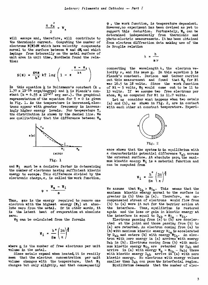
will escape and, therefore, will contribute tothe thermionic current. Computing the number ofelectrons N(W)dW which have velocity componentsnormal to the surface between W and dW, and whichimpinge from internally on the metal surface ofunit area in unit time, Nordheim found the rela-tion:
N(W) =4nm kT log 1 - Eh8
W - Wkt
In this equation k is Boltzmann's constant (k1.37 x 10-16 ergs/degree) and h is Planck's con-stant (h = 6.55 x 10⁻²⁷ erg sec.). The graphicalrepresentation of the equation for T = 0 is givenin Fig. 1. As the temperature is increased,elec-trons appear with greater frequency in increas-ingly higher energy levels. For temperature T,the distribution is shown by the dashed line. Wesee qualitatively that the difference between Wa
W
ENERGY
Fig. 1
and Wi must be a decisive factor in determining
T , the work function, is temperature dependent.However, no experiment has been devised as yet tosupport this deduction. Fortunately, Wa can bedetermined independently from thermionic andphoto -electric measurements. It has been obtainedfrom electron diffraction data making use of thede Broglie relation
connecting the wavelength A, the electron ve-locity v, and its mass m. In this equation h isPlanck's constant. Davison and Germer carriedout this measurement and found that Wa for Niwas 16.5 to 18 volts. Since the work functionof Ni- 5 volts, Wi would come out to be 11 to13 volts. If we assume two free electrons peratom, Wi as computed for Ni is 11.7 volts.
Let us consider what happens when two metals(a) and (b), as shown in Fig. 2, are in contactwith each other at constant temperature. Experi-
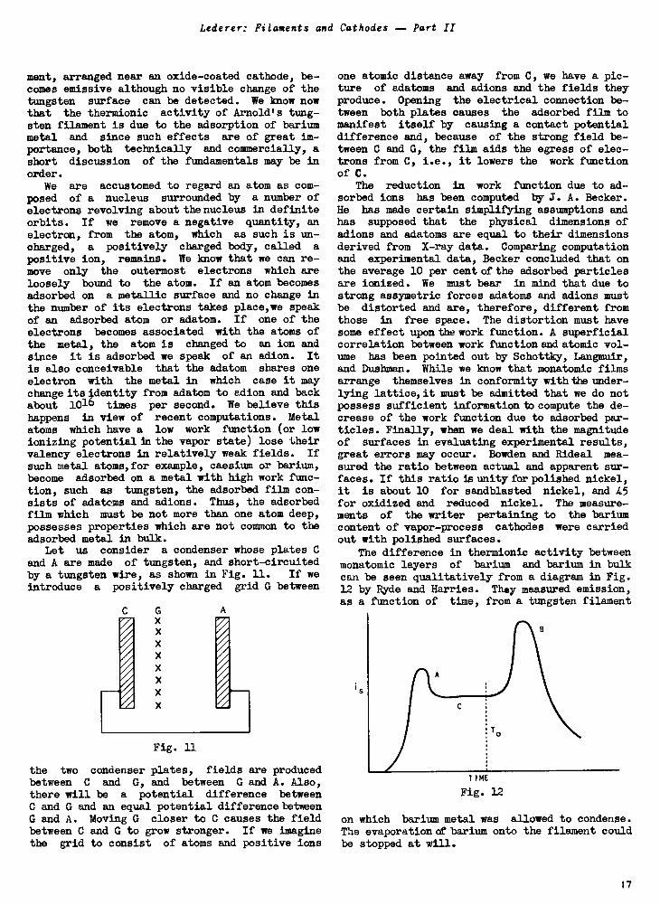
Fig. 2
ence shows that the system is in equilibrium witha characteristic potential difference Vab acrossthe external surface. At absolute zero, the maxi-mum kinetic energy Wi is a material function andcan be computed from
the number of electrons having sufficient kineticenergy to escape. This difference divided by theelectronic charge,e, is called the work function, Wi =
h 3 ( 311
8m n
Wa
e
Thus, pxe is the energy required to remove oneelectron with the highest energy (Wi) at abso-lute zero from the metal. Or in other words, itis the latent heat of evaporation at absolutezero.
Wi can be calculated from the formula
he ( 311)1Wi
8m n
where n is the number of free electrons per unitvolume in the metal.
Since metals expand when heated, it is readilyseen that the electron concentration per unitvolume changes with the temperature, that Wichanges but only slightly, and that consequently
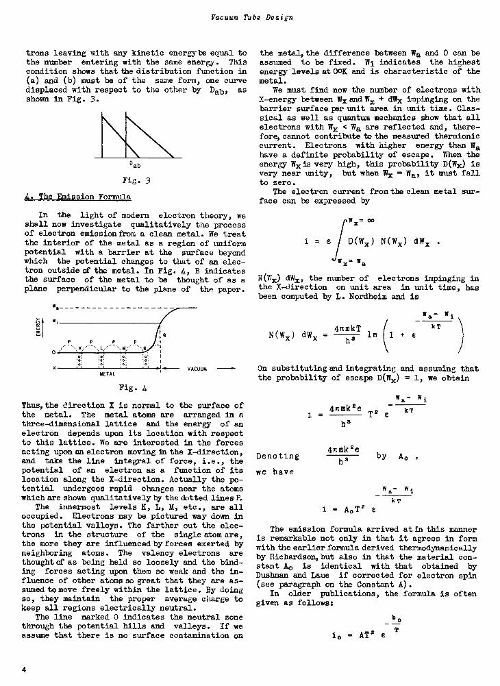
We assume that Wib > Wia. This means that themaximum kinetic energy normal to the surface isgreater in (b) than in (a). Therefore, an un-compensated stream of electrons would flow from(b) to (a) were it not for the barrier action atthe interface. Thus, equilibrium is restoredagain and the loss or gain in kinetic energy atthe interface is equal to Dab = Wi - Wib.
Electrons passing from (a) to (bY are acceler-ated at the joint and those passing from (b) to(a) are retarded. An electron coming from (a) to(b) with maximum kinetic energy Wia is acceleratedby Dab and enters (b) with energy Wib. An elec-tron with zero energy in (a) arrives with energyDab in (b). Electrons coming from (b) with maxi-mum kinetic energy Wib are retarded by Dab andarrive in (a) with energy Wa = Wib - Dab; thosewith kinetic energy Dab arrive in (a) with zerokinetic energy. No electrons with energy valuessmaller than Dab can pass the interfacial region.
Equilibrium demands that the number of elec-
3
Vacuum Tube Design
trons leaving with any kinetic energy be eaual tothe number entering with the same energy. Thiscondition shows that the distribution function in(a) and (b) must be of the same form, one curvedisplaced with respect to the other by Dab, as
shown in Fig. 3.
Dab
Fig. 3
4. The Emission Formula
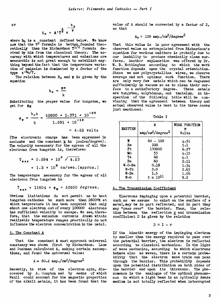
In the light of modern electron theory, weshall now investigate qualitatively the processof electron emissionfrom a clean metal. We treatthe interior of the metal as a region of uniformpotential with a barrier at the surface beyondwhich the potential changes to that of an elec-tron outside of the metal. In Fig. 4, B indicatesthe surface of the metal to be thought of as aplane perpendicular to the plane of the paper.
wa
1.1.1
O
METAL
Fig. 4
VACUUM
Thus, the direction X is normal to the surface ofthe metal. The metal atoms are arranged in athree-dimensional lattice and the energy of anelectron depends upon its location with respectto this lattice. We are interested in the forcesacting upon an electron moving in the X -direction,and take the line integral of force, i.e., thepotential of an electron as a function of itslocation along the X -direction. Actually the po-tential undergoes rapid changes near the atomswhich are shown qualitatively by the dotted lines P.
The innermost levels K, L, M, etc., are alloccupied. Electrons may be pictured way down inthe potential valleys. The farther out the elec-trons in the structure of the single atom are,the more they are influenced by forces exerted byneighboring atoms. The valency electrons arethought of as being held so loosely and the bind-ing forces acting upon them so weak and the in-fluence of other atoms so great that they are as-sumed to move freely within the lattice. By doingso, they maintain the proper average charge tokeep all regions electrically neutral.
The line marked 0 indicates the neutral zonethrough the potential hills and valleys. If weassume that there is no surface contamination on
the metal, the difference between Wa and 0 can beassumed to be fixed. Wi indicates the highestenergy levels at 00K and is characteristic of themetal.
We must find now the number of electrons withX -energy between WxandWx + dWx impinging on thebarrier surface per unit area in unit time. Clas-sical as well as quantum mechanics show that allelectrons with WX < Wa are reflected and, there-fore, cannot contribute to the measured thermioniccurrent. Electrons with higher energy than Wahave a definite probability of escape. When theenergy WxiS very high, this probability D(Wx) isvery near unity, but when Wx = Wa, it must fallto zero.
The electron current from the clean metal sur-face can be expressed by
N(Wx) dWx, the number of electrons impinging inthe X -direction on unit area in unit time, hasbeen computed by L. Nordheim and is
N(Wx) dWx -4nmkT
Inh3
Ws- Wi
kT(1 + e
On substituting and integrating and assuming thatthe probability of escape D(Wx) = 1, we obtain
Denoting
we have
Ws- Wi4nmk2e kT
h3
4nmk2e
h3
i = A0T2 e
by Ao ,
Wa- Wi
kT
The emission formula arrived at in this manneris remarkable not only in that it agrees in formwith the earlier formula derived thermodynamicallyby Richardson, but also in that the material con-stant Ao is identical with that obtained byDushman and Laue if corrected for electron spin(see paragraph on the Constant A).
In older publications, the formula is oftengiven as follows:
b
= AT2 e P
4
Lederer: Filaments and Cathodes -- Part I
Or
10 = A'T2
bo
where bo is a constant defined below. We knownow that the T2 formula is better founded theo-retically than the Richardson T1/2 formula de-rived by him from the classical theory. The ac-curacy with which temperatures and emissions aremeasurable is not great enough to establish any-thing beyond the fact that the temperature varia-tion of emission is dominated by a factor of thetype a-boiT.
The relation between Bo and 9 is given by theequation
peb, = -
k
Substituting the proper value for tungsten, weget for ITI/
(Pw
bok= -
q
52600 x 1.371 x 10 2s
1.591 x 10-19
= 4.53 volts
(The electronic charge has been expressed in
coulombs and the constant k in joules/degree).The velocity necessary for the egress of all theelectrons from tungsten is, therefore:
Vmaz = 0.594 x 10⁸ ri7-5
= 1.3 x 108 cm/sec.(approx.)
The temperature necessary for the egress of allelectrons from tungsten is
T max = 11604 x pw = 52600 degrees.
Obvious limitations do not permit us to heattungsten cathodes to much more than 28000K atwhich temperature it has been computed that onlyabout one electron out of every 100000 electronshas sufficient velocity to escape. We see,there -fore, that the emission currents drawn withinrealizable temperature ranges practically do notinfluence the electron concentration in the metal.
5. The Constant A
That the constant A must approach universalconstancy was shown first by Richardson. Laueand Dushman calculated A, making certain assump-tions, and found the universal value:
A = 60.2 amp ./cm2/degree2
Recently, in view of the electron spin, dis-covered by A. Compton and by means of whichPauli could account for the magnetic propertiesof the alkali metals, it has been found that the
value of A should be corrected by a factor of 2,so that
Ao = 120 amp./cm2/degree2
That this value is in poor agreement with theobserved value as extrapolated from Richardson'sequation for various emitters is probably due toour inability to produce chemically clean sur-faces. Another explanation was offered by Dr.W. B. Nottingham according to which the workfunction depends upon the crystal orientation.Since we use polycrystalline wires, we observeaverage and not optimum work function. Thereare only very few metals which can be degassedsufficiently in vacuum so as to clean their sur-face to a satisfactory degree. These metalsare tungsten, molybdenum, and tantalum. An in-spection of the following table will be con-vincing that the agreement between theory andactual observed value is best in the three casesjust mentioned.
Table I
EMITTERA
amp/cm2/degree2
WORK FUNCTION
PVolts
W 60 - 100 4.54Re 200 5.1Pt 170000 6.27Mo 55 4.15Ta 60 4.1Ba 60 2.11
W-O-Ba 0.18 1.34W-Th 3.0 2.63W-Ba 1.5 1.56W-0 5 x 10¹¹ 9.2
6. The Transmission Coefficient
Electrons impinging upon a potential barrier,such as we assume to exist on the surface of ametal, may be in part reflected, and in part theymay "pass over" the barrier. Thus, the rela-tion between the reflection r and transmissioncoefficient D is given by the relation
D = 1 - r
If the kinetic energy of the impinging electronis smaller than the energy required to pass overthe potential barrier, the electron is reflectedaccording to classical mechanics. In the lightof wave mechanics, according to which electronsbehave also as waves, there is a certain proba-bility that the electron wave train can passthrough the barrier. This probability dependsupon the potential distribution on both sides ofthe barrier and upon its thickness. The phe-nomenon is the analogue of the optical phenome-non in which a light beam in an optically densemedium is not totally reflected when interrupted
5
Vacuum Tube Design
by a layer of optically less dense material pro-vided the latter's thickness does not exceed a
few wavelengths. For practical purposes and
always if the kinetic energy of the impingingelectron is larger than the height of the barrier,the transmission coefficient is very nearly unityand, therefore, has been neglected in our emis-sion formula.
In making certain simplifying assumptions,Dushman has calculated the thickness of the po-tential barrier on thoriated tungsten and foundit not to exceed 3 angstroms. Since the diameterof a thorium atom is 5.1 angstroms, the correla-tion appears to be satisfactory.
We must remember, however, and this is wellsupported by observation, that a minute surfacecontamination on the emitter may change both thework function and the constant A profoundly. Weseek the explanation in the shape and height ofthe potential barrier and may expect more prac-tical information from a study of surface con-tamination by electron diffraction.
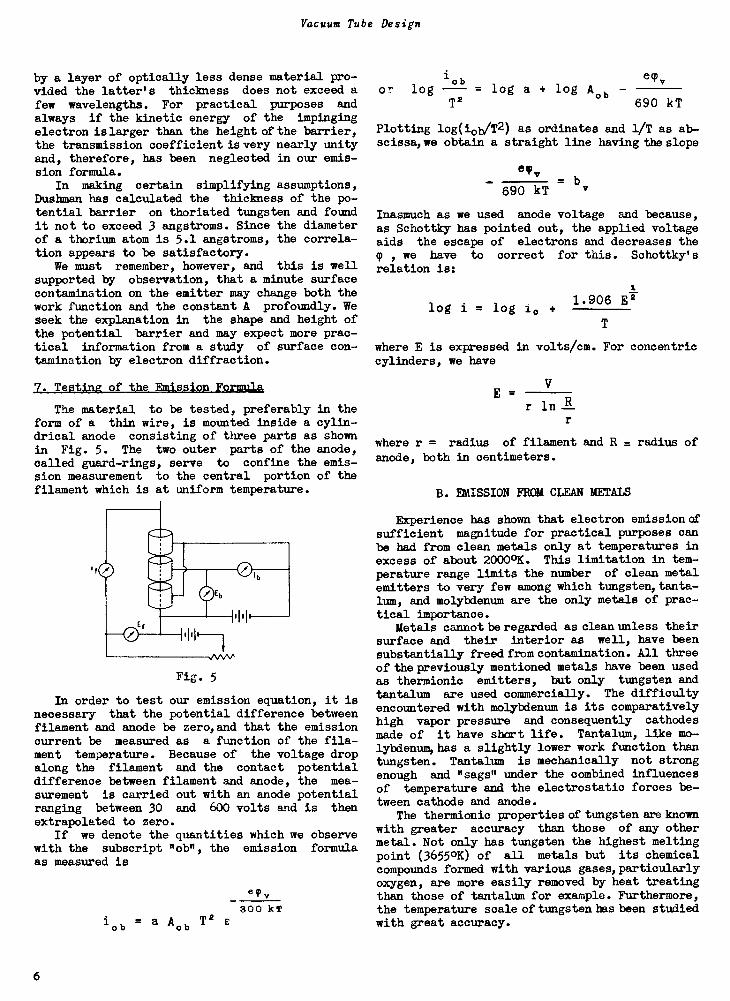
7. TestinE of the Emi sion Formula
The material to be tested, preferably in theform of a thin wire, is mounted inside a cylin-drical anode consisting of three parts as shownin Fig. 5. The two outer parts of the anode,called guard -rings, serve to confine the emis-sion measurement to the central portion of thefilament which is at uniform temperature.
if
Fig. 5
In order to test our emission equation, it isnecessary that the potential difference betweenfilament and anode be zero,and that the emissioncurrent be measured as a function of the fila-ment temperature. Because of the voltage dropalong the filament and the contact potentialdifference between filament and anode, the mea-surement is carried out with an anode potentialranging between 30 and 600 volts and is thenextrapolated to zero.
If we denote the quantities which we observewith the subscript "ob", the emission formulaas measured is
job a Aob 72 E
v
300 kT
lob e91,
or log - log a + log Aob -T2 690 kT
Plotting log( ia/T2) as ordinates and 1/7 as ab-scissa, we obtain a straight line having the slope
cc,690 kT
- b
Inasmuch as we used anode voltage and because,as Schottky has pointed out, the applied voltageaids the escape of electrons and decreases the9 , we have to correct for this. Schottky'srelation is:
log i = log 10 +1.906 E2
where E is expressed in volts/cm. For concentriccylinders, we have
VE -
r lo iLr
where r = radius of filament and R = radius of
anode, both in centimeters.
B. EMISSION FROM CLEAN METALS
Experience has shown that electron emission of
sufficient magnitude for practical purposes canbe had from clean metals only at temperatures inexcess of about 20000K. This limitation in tem-perature range limits the number of clean metalemitters to very few among which tungsten,tanta-lum, and molybdenum are the only metals of prac-tical importance.
Metals cannot be regarded as clean unless theirsurface and their interior as well, have beensubstantially freed from contamination. All threeof the previously mentioned metals have been usedas thermionic emitters, but only tungsten and
tantalum are used commercially. The difficultyencountered with molybdenum is its comparativelyhigh vapor pressure and consequently cathodes
made of it have short life. Tantalum, like mo-lybdenum, has a slightly lower work function thantungsten. Tantalum is mechanically not strongenough and "sags" under the combined influencesof temperature and the electrostatic forces be-tween cathode and anode.
The thermionic properties of tungsten are known
with greater accuracy than those of any othermetal. Not only has tungsten the highest meltingpoint (36550K) of all metals but its chemicalcompounds formed with various gases, particularlyoxygen, are more easily removed by heat treatingthan those of tantalum for example. Furthermore,the temperature scale of tungsten has been studiedwith great accuracy.
6
Lederer: Filaments and Cathodes -- Part I
In high -power transmitting tubes, tungsten isthe only metal rugged enough to withstand all themechanical and chemical requirements. As seenfrom Table I, the work function of tungsten in-creases more than twofold after exposure to oxy-gen. Although the oxygen contamination can be
removed by heating the tungsten to a temperaturein excess of 18000K, it is obvious in order tomaintain a steady emission level with respect to
small diameter. Wires of larger size can beoperated at a higher temperature for the percent-age loss due to evaporation becomes smaller withincreasing bulk of the emitters.
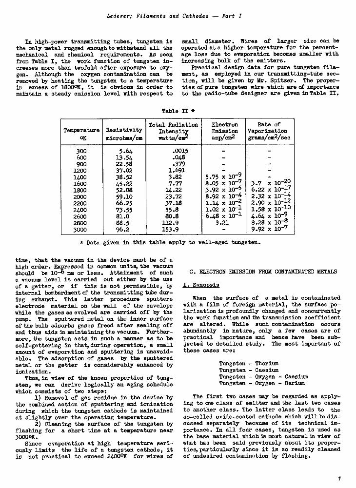
Practical design data for pure tungsten fila-ment, as employed in our transmitting -tube sec-tion, will be given by Mr. Spitzer. The proper-ties of pure tungsten wire which are of importanceto the radio -tube designer are given in Table II.
Table II *
Temperature
OK
Resistivity
microhms/cm
Total RadiationIntensitywatts/0E1z
ElectronEmissionamp/cm2
Rate ofVaporizationgrams/cmg/sec
300 5.64 .0015 - -600 13.54 .048 - -
900 22.58 .379 - -1200 37.02 1.691 - -
1400 38.52 3.82 5.75 x 10⁻⁷ -
1600 45.22 7.77 8.05 x 10⁻⁷ 3.7 x 10-201800 52.08 14.22 3.92 x 10⁻⁵ 6.22 x 10⁻¹⁷
2000 59.10 23.72 8.92 x 10⁻⁴ 2.32 x 10⁻¹⁴
2200 66.25 37.18 1.14 x 10⁻² 2.90 x 10⁻¹²
2400 73.55 55.8 1.02 x 10⁻¹ 1.58 x 10⁻¹⁰
2600 81.0 80.8 6.48 x 10⁻¹ 4.64 x 10⁻⁹
2800 88.5 112.9 3.21 8.28 x 10⁻⁸
3000 96.2 153.9 - 9.92 x 10⁻⁷
* Data given in this table apply to well -aged tungsten.
time, that the vacuum in the device must be of ahigh order. Expressed in common units, the vacuumshould be 10-b mm or less. Attainment of sucha vacuum level is carried out either by the useof a getter, or if this is not permissible, byinternal bombardment of the transmitting tube dur-ing exhaust. This latter procedure sputters
electrode material on the wall of the envelopewhile the gases as evolved are carried off by thepump. The sputtered metal on the inner surfaceof the bulb adsorbs gases freed after sealing offand thus aids in maintaining the vacuum. Further-more, the tungsten acts in such a manner as to beself-gettering in that, during operation, a smallamount of evaporation and sputtering is unavoid-able. The adsorption of gases by the sputteredmetal or the getter is considerably enhanced byionization.
Thus, in view of the known properties of tung-sten, we can derive logically an aging schedulewhich consists of two steps:
1) Removal of gas residue in the device bythe combined action of sputtering and ionizationduring which the tungsten cathode is maintainedat slightly over the operating temperature.
2) Cleaning the surface of the tungsten byflashing for a short time at a temperature near30000K.
Since evaporation at high temperature seri-ously limits the life of a tungsten cathode, itis not practical to exceed 24000K for wires of
C. ELECTRON EMISSION FROM CONTAMINATED METALS
1. Synopsis
When the surface of a metal is contaminatedwith a film of foreign material, the surface po-larization is profoundly changed and concurrentlythe work functionsmditistransmission coefficientare altered. While such contamination occursabundantly in nature, only a few cases are ofpractical importance and hence have been sub-jected to detailed study. The most important ofthese cases are:
Tungsten - ThoriumTungsten - CaesiumTungsten - Oxygen - CaesiumTungsten - Oxygen - Barium
The first two cases may be regarded as apply-ing to one class of emitter and the last two casesto another class. The latter class leads to theso-called oxide -coated cathode which will be dis-cussed separately because of its technical im-portance. In all four cases, tungsten is used asthe base material which is most naturalin view ofwhat has been said previously about its proper-ties, particularly since it is so readily cleanedof undesired contamination by flashing.
7
Vacuum Tube Design
2. Thoriated Tungsten
a. The Main Phenomenon -- In order to preventoffsetting, tungsten filaments were "doped" with0.75 to 2% thoria even in the early stages oftungsten incandescent -lamp manufacture. In 1913Langmuir and Rogers discovered that the thermionicemission of such "thoria -doped filaments" was,after certain treatment, several thousand timeslarger than the emission of a pure tungsten fila-ment under the same conditions. Various treat-ments were tried but the one finally adopted toobtain maximum thorium emission is as follows:
The filament is flashed for a minute or twoat a temperature higher than 2700°K to reducesome of the thoria in the wire to thorium metal.At this high temperature, any impurity on thesurface of the wire is vaporized. Any thoriummetal diffusing to the surface is immediatelyevaporated so that the activity of the filamentis substantially that of pure tungsten.
If now the temperature is reduced to a valuebetween 2000° and 2200°K, the rate of diffusionis quite high but the rate of evaporation is de-creased to such an extent that thorium atoms canaccumulate on the surface as an adsorbed layer.In order that the rate at which the surface be-comes covered with thorium can be observed, theemission is tested at frequent intervals at a
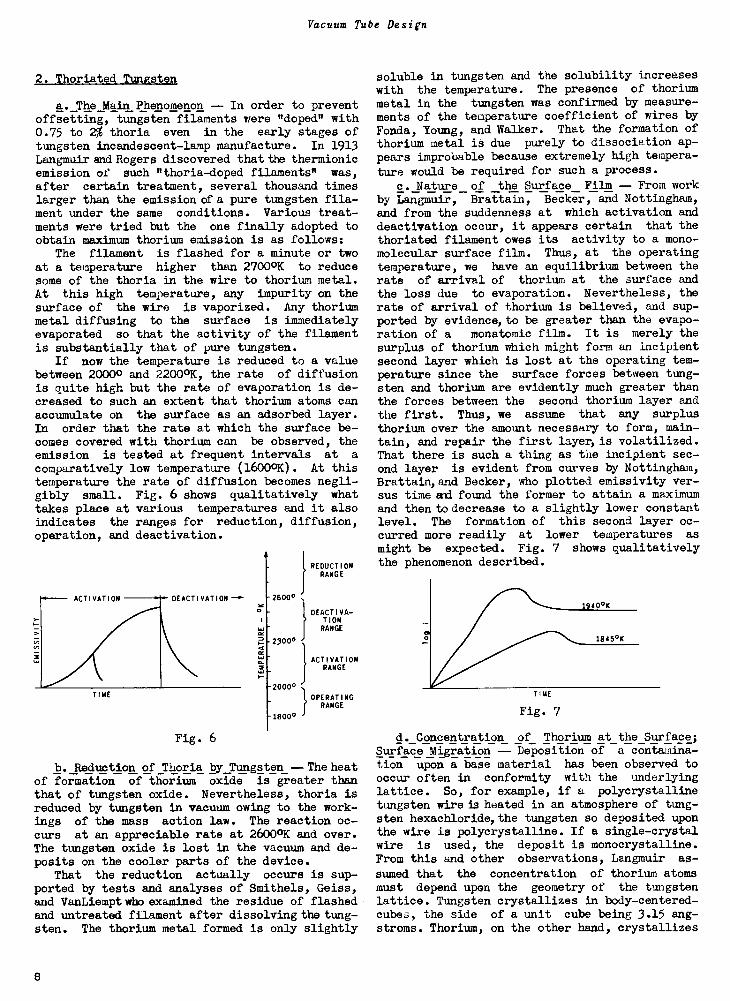
comparatively low temperature (16000K). At thistemperature the rate of diffusion becomes negli-gibly small. Fig. 6 shows qualitatively whattakes place at various temperatures and it alsoindicates the ranges for reduction, diffusion,operation, and deactivation.
ACTIVATION DEACTIVATION
TIME
Fig. 6
O
-2600°
-2300°
REDUCTIONRANGE
DEACTIVA-TIONRANGE
ACTIVATIONRANGE
-2000°
1800°
OPERATINGRANGE
b. Reduction of Thoria 1217 Tungsten - The heatof formation of thorium oxide is greater thanthat of tungsten oxide. Nevertheless, thoria isreduced by tungsten in vacuum owing to the work-ings of the mass action law. The reaction oc-curs at an appreciable rate at 26000K and over.The tungsten oxide is lost in the vacuum and de-posits on the cooler parts of the device.
That the reduction actually occurs is sup-ported by tests and analyses of Smithels, Geiss,and VanLiempt who examined the residue of flashedand untreated filament after dissolving the tung-sten. The thorium metal formed is only slightly
soluble in tungsten and the solubility increaseswith the temperature. The presence of thorium
metal in the tungsten was confirmed by measure-ments of the temperature coefficient of wires byFonda, Young, and Walker. That the formation of
thorium metal is due purely to dissociation ap-pears improbable because extremely high tempera-
ture would be required for such a process.
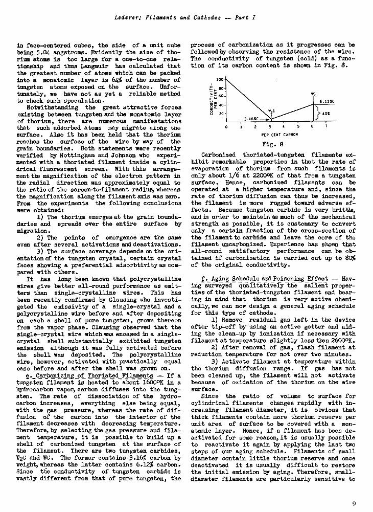
c. Nature of the Surface Film -- From workby Langmuir, Brattain, Becker, and Nottingham,and from the suddenness at which activation anddeactivation occur, it appears certain that the
thoriated filament owes its activity to a mono -
molecular surface film. Thus, at the operating
temperature, we have an equilibrium between therate of arrival of thorium at the surface andthe loss due to evaporation. Nevertheless, therate of arrival of thorium is believed, and sup-ported by evidence, to be greater than the evapo-ration of a monatomic film. It is merely thesurplus of thorium which might form an incipientsecond layer which is lost at the operating tem-perature since the surface forces between tung-sten and thorium are evidently much greater thanthe forces between the second thorium layer and
the first. Thus, we assume that any surplus
thorium over the amount necessary to form, main-tain, and repair the first layer, is volatilized.That there is such a thing as the incipient sec-ond layer is evident from curves by Nottingham,Brattain,and Becker, who plotted emissivity ver-sus time and found the former to attain a maximumand then to decrease to a slightly lower constantlevel. The formation of this second layer oc-curred more readily at lower temperatures as
might be expected. Fig. 7 shows qualitativelythe phenomenon described.
TIME
Fig. 7
d. Concentration of Thorium at the Surface;Surface Migration -- Deposition of a contamina-tion upon a base material has been observed tooccur often in conformity with the underlyinglattice. So, for example, if a polycrystallinetungsten wire is heated in an atmosphere of tung-sten hexachloride,the tungsten so deposited uponthe wire is polycrystalline. If a single -crystalwire is used, the deposit is monocrystalline.From this and other observations, Langmuir as-
sumed that the concentration of thorium atomsmust depend upon the geometry of the tungstenlattice. Tungsten crystallizes in body -centered -cubes, the side of a unit cube being 3.15 ang-stroms. Thorium, on the other hand, crystallizes
8
Lederer: Filaments and Cathodes -- Part I
in face -centered cubes, the side of a unit cubebeing 5.04 angstroms. Evidently the size of tho-rium atoms is too large for a one-to-one rela-tionship and thus Langmuir has calculated thatthe greatest number of atoms which can be packedinto a monatomic layer is 64% of the number oftungsten atoms exposed on the surface. Unfor-tunately, we have not as yet a reliable methodto check such speculation.
Notwithstanding the great attractive forcesexisting between tungsten and the monatomic layerof thorium, there are numerous manifestationsthat such adsorbed atoms may migrate along thesurface. Also it has been held that the thoriumreaches the surface of the wire by way of thegrain boundaries. Both statements were recentlyverified by Nottingham and Johnson who experi-mented with a thoriated filament inside a cylin-drical fluorescent screen. With this arrange-menttba magnification of the electron pattern inthe radial direction was approximately equal tothe ratio of the screen -to -filament radius, whereas
the magnification along the filamentamiswas2erh.From the experiments the following conclusionswere obtained:
1) The thorium emerges at the grain bounda-daries and spreads over the entire surface bymigration.
2) The points of emergence are the sameeven after several activations and deactivations.
3) The surface coverage depends al the ori-entatiancf the tungsten crystal, certain crystalfaces showing a preferential adsorbtivity as com-pared with others.
It has long been known that polycrystallinewires give better all-round performance as emit-ters than single -crystalline wires. This hasbeen recently confirmed by Clausing who investi-gated the emissivity of a single -crystal and apolycrystalline wire before and after depositingon each a shell of pure tungsten, grown thereonfrom the vapor phase. Clausing observed that thesingle -crystal wire which was encased Ina single -
crystal shell substantially exhibited tungstenemission although it was fully activated beforethe shell was deposited. The polycrystallinewire, however, activated with practically equalease before and after the shell was grown on.
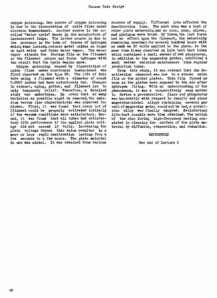
e._Carbonizity of Thoriated Filaments -- If atungsten filament is heated to about 16000K in ahydrocarbon vapor, carbon diffuses into the tung-sten. The rate of dissociation of the hydro-carbon increases, everything else being equal,with the gas pressure, whereas the rate of dif-fusion of the carbon into the interior of thefilament decreases with decreasing temperature.Therefore, by selecting the gas pressure and fila-ment temperature, it is possible to build up ashell of carbonized tungsten at the surface ofthe filament. There are two tungsten carbides,W2C and WC. The former contains 3.16% carbon byweight, whereas the latter contains 6.12% carbon.Since the conductivity of tungsten carbide isvastly different from that of pure tungsten, the
process of carbonization as it progresses can befollowed by observing the resistance of the wire.The conductivity of tungsten (cold) as a func-tion of its carbon content is shown in Fig. 8.
100
80
w60
2..a.40
a20
PER CENT CARBON
Fig. 8
Carbonized thoriated-tungsten filaments ex-hibit remarkable properties in that the rate ofevaporation of thorium from such filaments isonly about 1/6 at 22000K of that from a tungstensurface. Hence, carbonized filaments can beoperated at a higher temperature and, since therate of thorium diffusion can thus be increased,the filament is more rugged toward adverse ef-fects. Because tungsten carbide is very brittle,andin order to maintain as much of the mechanicalstrength as possible, it is customary to convertonly a certain fraction of the cross-section ofthe filament to carbide and leave the core of thefilament uncarbonized. Experience has shown thatall-round satisfactory performance can be ob-tained if carbonization is carried out up to 80%of the original conductivity.
f. AginE Schedule and Poisoning Effect -- Hav-ing surveyed qualitatively the salient proper-ties of the thoriated-tungsten filament and bear-ing in mind that thorium is very active chemi-cally, we can now design a general aging schedulefor this type of cathode.
1) Remove residual gas left in the deviceafter tip-off by using an active getter and aid-ing the clean-up by ionization if necessary withfilament at temperature slightly less than 26000K.
2) After removal of gas, flash filament atreduction temperature for not over two minutes.
3) Activate filament at temperature withinthe thorium diffusion range. If gas has notbeen cleaned up, the filament will not activatebecause of oxidation of the thorium on the wiresurface.
Since the ratio of volume to surface forcylindrical filaments changes rapidly with in-creasing filament diameter, it is obvious thatthick filaments contain more thorium reserve perunit area of surface to be covered with a mon-atomic layer. Hence, if a filament has been de-activated for some reason, it is usually possibleto reactivate it again by applying the last twosteps of our aging schedule. Filaments of smalldiameter contain little thorium reserve and oncedeactivated it is usually difficult to restorethe initial emission by aging. Therefore, small -diameter filaments are particularly sensitive to
9
Vacuum Tube Design
oxygen poisoning. One source of oxygen poisoningis due to the dissociation of oxide films underelectron bombardment. Another source is the so-called "water cycle" known in the manufacture ofincandescent lamps. The latter source is due tothe presence in the tube of traces of hydrogenwhich, when ionized, reduces metal. oxides as foundon spot welds and forms water vapor. The watervapor attacks the thorium film on the filamentor the filament proper and forms hydrogen withthe result that the cycle begins anew.
Oxygen poisoning caused by dissociation ofoxide films under electronic bombardment wasfirst observed on the type 99. The life of thistube using a filament with a diameter of about0.0007 inches had been notoriously bad. Changesin exhaust, aging, getter, and filament led to
only temporary relief. Therefore, a detailedstudy was undertaken. In order that as manyvariables as possible might be removed, the emis-sion versus time characteristic was observed fordiodes. First, it was found that every lot offilament could be properly activated initiallyif the vacuum conditions were satisfactory. Sec-ond, it was found that all tubes had satisfac-tory life performance if the applied plate volt-age did not exceed 13 volts. Increasing theplate voltage beyond this value resulted in amore or less rapid deactivation lasting from a
few seconds to a few hours. The plate materialin use was nickel. It was obtained from various
sources of supply. Different lots affected thedeactivation time. The next step was a test ofother plate materials, end so iron, zinc, silver,and platinum were tried. Of these, the last threehad no effect upon the filament, the emissivityremaining constant for several hundred hours withas much as 50 volts applied to the plate. At thesame time it was observed on life test that tubeswhich contained a small amount of red phosphorus,in addition to the magnesium getter, exhibited amuch better emission maintenance than regularproduction tubes.
From this study, it was evident that the de-activation observed was due to a minute oxidefilm on the nickel plates. This film formed assoon as the plates were exposed to the air afterhydrogen firing. With an understanding of thephenomenon, it was a comparatively easy matterto devise a preventative. Since red phosphoruswas too erratic with respect to results and sincemagnesium -nickel alloys containing several percent of magnesium metal could not be had, a nickel -
zinc alloy was finally adopted. Satisfactorylife -test results were then obtained. The actionof the zinc during high -frequency heating con-sisted in cleaning the surface of the plate ma-terial by diffusion, evaporation, and reduction.
REFERENCES
See end of Lecture 2
I0
Lecture 2
FILAMENTS AND CATHODES -- Part II
E. A. Lederer
OXIDE -COATED CATHODES
}. Introduction
In the first lecture we discussed the escapeof electrons from clean and contaminated metalsand we noticed the enormous difference in workfunction caused by monatomic layers of two dif-ferent materials on a clean metal surface. Com-paring for example thoriated and oxidized tung-sten whose fork functions are 2.6 and 9.2 volts,respectively, we find that the emission of theformer is several millionfold greater than thelatter at the same operating temperature. Theoxide -coated cathode is but a special case of acontaminated surface and because of its commercialimportance deserves considerable discussion.
The first question suggesting itself is: Whatis the definition of an oxide -coated cathode?Because of the complexity of the article, bothfrom the physical and chemical viewpoint, no suchdefinition can be given at present. It seemslogical to review at first methods of preparationand properties before attempting to define sucha cathode. The definition will at best describeonly certain salient points because our knowledgeof this subject is far from complete.
The oxide -coated cathode was discovered in1903 by A. Wehnelt, who was studying gas dis-charges at that time and observed a considerabledecrease of the so-called cathode fall, when thecathode was accidentally coated with certain im-purities. A careful study of the impurities re-vgaled the presence of calcium compounds and aftermph experimentation Wehnelt found that the oxidesof calcium, strontium, and barium were responsi-ble for the observed effects. All three elementsconstitute the group of the so-called alkaline -earth metals. When speaking of an oxide -coatedcathode, we mean a metal surface which can beheated and which is coated with any one of theoxides of calcium, strontium or barium; or witha mixture of two or three of these oxides. Morerecently the meaning of an oxide -coated cathodehas been confined to one coated with barium andstrontium oxides only since both exhibit electronemission in a greater degree than calcium oxide.
For ten years after its inception, the oxide -coated cathode remained in the laboratory of thephysicist as the object of some study and of muchcontroversy. Shortly before the war, the cathodewas developed commercially to be used in tele-phone repeater tubes by the Bell Telephone Labo-ratories. The coating developed for this purposewas sintered in air upon a platinum alloy servingas the base material. Part of the base was dis-persed in and combined with the coating with theresult that the coating had a gray to black ap-pearance. Hence, this coating was known as thecombined coating and because of its dark color,
required an input of 6 to 8 watts/cmg to maintainit at the proper operating temperature.
It was not until about 1925 that the techniqueof controlling a white uncombined coating wasmastered to such an extent as to make use of itcommercially. In the past 10 or 15 years, thetechnique has been greatly improved and with itthe efficiencycf the uncombined coating has beenincreased. Hence, the input required is smallerthan 4 watts/cmg with a lower limit of approxi-mately 1 watt/cm2. The lower the cathode tempera-ture, the more sensitive is the coating towardthe effects of gaseous residues in the tube and,therefore, commercial cathodes are designed tooperate at not less than 2.5 watts/ma. Thishigh thermionic efficiency is the main reason whythe uncombined coating is finding ever-increasinguse in thermionic devices. Another very importantadvantage of the uncombined coating is its easeof application by dipping or spraying on a metalsurface of any desired shape. Since the thermi-onic activity is confined strictly to the coatedsection and does not extend onto uncoated sec-tions of the metallic base, it is possible to de-sign tubes with well-defined coated -cathode areas.Such well-defined areas make it relatively easyto obtain definite.values of cut-off, plate cur-rent, and transconductance.
In the following, the term "oxide -coated cath-ode" means an uncombined coating consisting ofbarium and strontium oxide on a metallic base.
2. Preparation of Oxide -Coated Cathodes
Since barium or strontium oxides are unstablein air and combine rapidly with moisture andcarbon dioxide, it is commercially impossible touse these oxides as such for the preparation ofthe coating. Fortunately, there are a number ofchemical compounds of the Rimline-earth metalswhich are stable in air and which when heated invacuum decompose to the oxides. The best com-pounds are the carbonates because they have therequired stability and can be obtained very pure.They are inexpensive and besides the oxides, theonly decomposition product is carbon dioxidewhich, being a gas, can be removed by the vacuumpump. For example, barium carbonate can be writ-ten by its constitution formula
Ba.--t 13-0Ba0 + CO2-----
and decomposes as indicated by the dotted lineand arrow into barium oxide and carbon dioxide atelevated temperature. The decomposition tempera-ture is different for all three of the alkaline-earth metals. The relation between dissociationpressure in millimeters of mercury and tempera-ture for magnesium, calcium, and barium carbon-
I,
Vacuum Tube Design
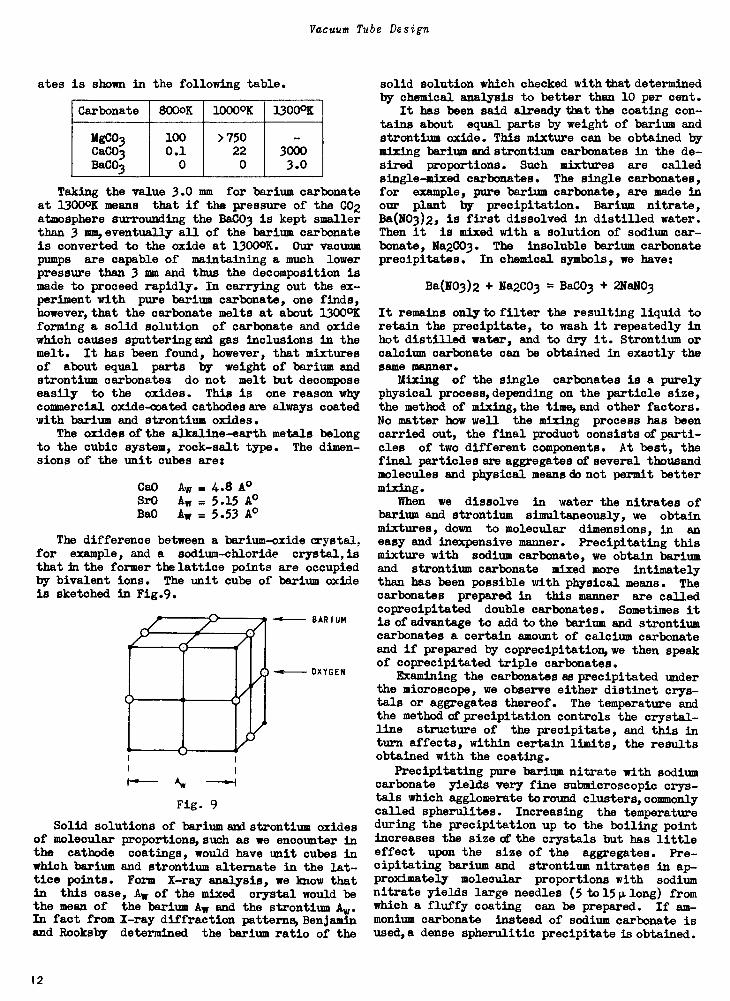
ates is shown in the following table.
Carbonate 8000K 1000°K 13000X
MgCO3 100 >750 -
CaCO3 0.1 22 3000BaCO3 0 0 3.0
Taking the value 3.0 mm for barium carbonateat 1300°K means that if the pressure of the CO2atmosphere surrounding the BaCO3 is kept smallerthan 3 mm, eventually all of the barium carbonateis converted to the oxide at 13000K. Our vacuumpumps are capable of maintaining a much lowerpressure than 3 mm and thus the decomposition ismade to proceed rapidly. In carrying out the ex-periment with pure barium carbonate, one finds,however, that the carbonate melts at about 1300°Kforming a solid solution of carbonate and oxidewhich causes sputtering and gas inclusions in themelt. It has been found, however, that mixturesof about equal parts by weight of barium andstrontium carbonates do not melt but decomposeeasily to the oxides. This is one reason whycommercial oxide -coated cathodes are always coatedwith barium and strontium oxides.
The oxides of the alkaline -earth metals belongto the cubic system, rock -salt type. The dimen-sions of the unit cubes are:
Ca0Sr0Ba0
Aw - 4.8 A°Aw = 5.15 A°Aw = 5.53 A°
The difference between a barium -oxide crystal,for example, and a sodium -chloride crystal, is
that in the former the lattice points are occupiedby bivalent ions. The unit cube of barium oxideis sketched in Fig.9.
AW
BARIUM
OXYGEN
Fig. 9
Solid solutions of barium and strontium oxidesof molecular proportions, such as we encounter inthe cathode coatings, would have unit cubes inwhich barium and strontium alternate in the lat-tice points. Form X-ray analysis, we know thatin this case, Aw of the mixed crystal would bethe mean of the barium Aw and the strontium Aw.In fact from X-ray diffraction patterns, Benjaminand Rooksby determined the barium ratio of the
solid solution which checked with that determinedby chemical analysis to better than 10 per cent.
It has been said already that the coating con-tains about equal parts by weight of barium andstrontium oxide. This mixture can be obtained bymixing barium and strontium carbonates in the de-sired proportions. Such mixtures are calledsingle -mixed carbonates. The single carbonates,for example, pure barium carbonate, are made inour plant by precipitation. Barium nitrate,Ba(NO3)2, is first dissolved in distilled water.Then it is mixed with a solution of sodium car-bonate, Na2CO3. The insoluble barium carbonateprecipitates. In chemical symbols, we have:
Ba(NO3)2 + Na2CO3 = BaCO3 + 2NaNO3
It remains only to filter the resulting liquid toretain the precipitate, to wash it repeatedly inhot distilled water, and to dry it. Strontium orcalcium carbonate can be obtained in exactly thesame manner.
Mixing of the single carbonates is a purelyphysical process, depending on the particle size,the method of mixing, the time, and other factors.No matter how well the mixing process has beencarried out, the final product consists ofparti-ales of two different components. At best, thefinal particles are aggregates of several thousandmolecules and physical means do not permit bettermixing.
When we dissolve in water the nitrates ofbarium and strontium simultaneously, we obtainmixtures, down to molecular dimensions, in aneasy and inexpensive manner. Precipitating thismixture with sodium carbonate, we obtain bariumand strontium carbonate mixed more intimatelythan has been possible with physical means. Thecarbonates prepared in this manner are calledcoprecipitated double carbonates. Sometimes itis of advantage to add to the barium and strontiumcarbonates a certain amount of calcium carbonateand if prepared by coprecipitation, we then speakof coprecipitated triple carbonates.
Examining the carbonates as precipitated underthe microscope, we observe either distinct crys-tals or aggregates thereof. The temperature andthe method of precipitation controls the crystal-line structure of the precipitate, and this inturn affects, within certain limits, the resultsobtained with the coating.
Precipitating pure barium nitrate with sodiumcarbonate yields very fine submicroscopic crys-tals which agglomerate to round clusters, commonlycalled spherulites. Increasing the temperatureduring the precipitation up to the boiling pointincreases the size of the crystals but has littleeffect upon the size of the aggregates. Pre-cipitating barium and strontium nitrates in ap-proximately molecular proportions with sodiumnitrate yields large needles (5 tol5p.long) fromwhich a fluffy coating can be prepared. If am-monium carbonate instead of sodium carbonate isused,a dense spherulitic precipitate is obtained.
12
Lederer: Filaments and Cathodes -- Part II
In general, dense carbonates of spheruliticstructure are useful and desirable in close -spaced
rectifiers. Fluffy carbonates are used for coat-ing of cathodes for low -power receiving tubes.Single -mixed carbonates are used for coatingfilaments of all sizes and also make a good coat-ing for certain close -spaced rectifiers. Experi-ence has shown that fluffy coatings are generallyeasier to activate than dense coatings. The lat-ter type of coating, especially carbonates withapherulitic structure,sputters less readily whenused in rectifiers.
The carbonates can be coated onto a metallicbase by many methods. Two methods, because oftheir simplicity and ease of control are widelyused. They are: spraying, and coating by thedrag process. Spraying is used for coating in-directly heated cathodes and in rare cases forcoating filaments. The drag process is suitablefor filaments only.
The first method involving the use of a spraymixture consists in applying the carbonates sus-pended in a suitable binder by means of a spraygun. The spray mixture is prepared by ball -mill-ing the carbonates together with an organic ve-hicle for several hours (18 to 72 hours). Inorderly improve the adherence of the carbonates,it is customary to employ nitrocellulose as abinder; hence, the organic vehicle used should bea solvent of nitrocellulose. By the proper se-lection of the vehicle or the use of mixtures ofsolvents, the drying properties of the coatingcan be varied within wide limits. Slow -dryingsprays give dense, smooth coatings. Solventshaving a high vapor pressure at room temperatureare used to obtain fluffy coatings. The amountof nitrocellulose seldom exceeds 2 per cent byweight of the solid carbonates. Nitrocelluloseie to date the best binder we have because it de-composes at a low temperature (approximately200°C) without leaving any perceptible residue.This is because nitrocellulose does not dependsolely on the supply of oxygen from the atmospherefor combustion, but is partially self -combusting.
The second method, or drag process, is carriedout by applying the carbonate coating in succes-sive thin layers onto the filament and baking itbetween applications in carbon dioxide to about700°C. In this case the coating mixture is asuspension of the carbonates in water, and inorder to improve the adherence, barium and/orstrontium nitrate are added (up to10 per cent ofthe carbonates) to the solution. In the bakingoperation in CO2, the nitrates are converted tocarbonates and in this manner the coating parti-cles are cemented together. The coating processconsists of dragging the filament through thecoating mixture whichbycapillaryforces collectsin a groove of a slowly rotating small wheel whoselower section is immersed in the mixture. Inthis manner the mixture is agitated and a definiteamount of coating, controlled by viscosity andsurface tension, is transferred to the filament.
There is another method of coating which should
be mentioned. It is known as coating by cata-phoresis, and is applicable to filaments and in-directly heated cathodes. This method yieldscoatings of high density and is less flexiblethan the two methods previously described. Fur-thermore, with cataphoretically coated cathodes,it appears more difficult to meet the presentcommercial emission limits.
In describing the amount of coating on cath-odes, it is convenient to specify the weight ofthe coating in milligrams per cm2 of coated sur-face. Experience has shown that with a coatingweight of from 3 to 6 mg/cm2 satisfactory lifecan be obtained. Coatings which are heavier thanthe upper limit given above are difficult to de-gas.
It is of great importance that the coatingadhere well to the base material. If the coat-ing mixture does not wet the core during decompo-sition, blisters and air pockets are producedand cause poor electron and heat transfer in theoverlying coating.
Theoretically, it makes no difference how thecarbonate coating is applied onto the basematerial. Practically, however, in the manufac-ture of radio receiving tubes with a multitudeof variables,the task of reducing initial shrink-age and obtaining good quality is often facili-tated by selecting the proper coating and binderfor the particular purpose. This is the mainreason why a multitude of spray mixturesl havebeen devised and standardized in the course oftime.
3. Activation
Having reviewed methods for coating cathodes,we have already indicated that it is the finalgoal of all the chemical processes to produce,while maintaining the vacuum, an uncontaminatedcoating of barium and strontium oxides on thesurface of the cathode. Experience has shownthat such a coating exhibits the property ofelectron emission only after a more or less com-plicated activation schedule. In its activatedstate, the coating is indistinguishable micro-scopically (and chemically after removal fromthe bulb) from its unactivated form, and yet theelectron emission may differ by a factor of sev-eral millions. Our immediate interest is focusednow on what goes on during activation.
As early as 1920, Arnold found that the "ac-tive material" could be transferred from a well -activated filament to a cleaned -tungsten fila-ment arranged parallel and in close proximity tothe former. During this migration process whichrequired some time depending on the temperature,no thermionic activity of the donor filament waslost but the receptive tungsten filament builtup thermionic activity evidently from nothing.
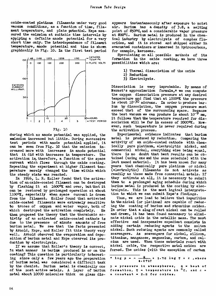
In 1924, W. Espe measured the activation of
1 Ref. 2-1
13
Vacuum Tube Design
oxide -coated platinum filaments under very goodvacuum conditions, as a function of time, fila-ment temperature, and plate potential. Espe mea-sured the emission at suitable time intervals byapplying a definite anode potential for a veryshort time only. The interdependence of filamenttemperature, anode potential and time is showngraphically in Fig. 10. In the first test period
15
10
EMISSIONCURRENT
MILL1AMP.
5
0
.,-....
100
..,100
.......
200
..-,...
300
/-
1-
0 10f
201 2 3 4 5
CATHODETEMP.-Pft
-6-PLATE VOLTS
-.HOURS.-TEST PERIOD
Fig. 10
during which no anode potential was applied, theemission increased but little. During successivetest periods with anode potential applied, itcan be seen from Fig. 10 that the emission in-creased more with increases in anode potentialthat it did with increases in temperature. Theactivation is, therefore, a function of the spacecurrent which flows through the oxide coating.Repeating the experiment at higher filament tem-perature merely changed the time within whichthe steady state was reached.
In 1926, L. R. Koller found that the activa-tion of an oxide -coated filament can be destroyedby flashing it at 1600°K and over, but that itcan be restored by prolonged operation at about11000K, especially when space current is drawnfrom the filament. Koller found that activatedoxide -coated filaments were extremely sensitiveto traces of oxygen and water vapor, both ofwhich destroyed the activation completely. He
then proposed the theory that the thermionic ac-tivity of an activated oxide -coated cathode isdue to the presence of minute amounts of freebarium metal. We see that the facts presentedby Arnold, Espe, and Koller fit this theory verywell. Arnold observed the evaporation and depo-sition arberium metal and Espe observed its pro-duction by electrolysis.
If we assume that Koller's theory is correct,in what manner is barium produced in or on thecoating? This question is particularly interest-ing since only a few years ago the preparationof barium metal was considered a difficult taskby the chemist. Barium metal is chemically oneof the most active metals. A layer of bariummetal about 10000 molecules thick on glass dis-
appears instantaneously after exposure to moistair. Barium has a density of 3.8, a meltingpoint of 8500C,and a considerable vapor pressureat 800°C. Barium metal is produced in the chem-ical industry by electrolysis of complex flu-orides, and it is stored and shipped either inevacuated containers a immersed in hydrocarbons,for example, kerosene.
Speculating on all possible methods of itsformation in the oxide coating, we have threepossibilities which are:
1) Thermal dissociation of the oxide2) Reduction3) Electrolysis.
Dissociation is very improbable. By means ofNernst's approximation formula,* we can computethe oxygen dissociation pressure at any desiredtemperature and find that at 10000K the pressureis about 10-30 microns. In order to produce bar-ium by dissociation, the oxygen pressure mustexceed that of the surrounding space. BeRausethe best vacuum we can produce is about 10-/ mm,it follows that the temperature required for dis-sociation will be far in excess of 20009K. How-ever, such temperature is never required duringthe activation process.
Experimental evidence indicates that bariummetal is produced by reduction. Comparing theactivity of an oxide -coated cathode with chem-ically pure platinum, electrolytic nickel, andcommercial nickel, everything else being equal,there is no doubt that best results can be ob-tained (using one and the same schedule) with thelast named material. It has been known for manyyears that chemically pure platinum or nickel(electrolytic) filaments do not activate asreadily as those made from commercial metals. Ifthey activate at all, it is necessary to submitthem to a prolonged aging schedule during whichbarium metal is produced in the coating by elec-trolysis. This is the most logical interpreta-tion to which we can submit Espe's findings.
Thus, we are lead to believe that impuritiesin the nickel (or platinum) are capable of reduc-ing the coating of barium and strontium oxides.In order that a slug of cast nickel can be rolledand drawn, it has been found necessary to elimi-nate nickel oxide in the metallic mass. The mosteffective and inexpensive expedient consists inadding certain reducing agents to the moltennickel. Such reducing agents are commonly calledscavengers. As scavengers for nickel, silicon,titanium, manganese, magnesium, carbon, and cal-cium are used. When these materials react withnickel oxide, the respective metal oxides areformed. The oxides (with the exception of carbon
log p = 1.75 log T + c ,where4.571T
p = pressureformation, Ta constant =
in atmospheres, Q =temperature in °C,
2.8 for oxides.
heat ofand c =
14
Lederer: Filaments and Cathodes -- Part II
dioxide) are expelled by the molten nickel andform a slag on top of the melt. Adding thescavengers, of which only one or two of the namedmaterials are used, is an art and is left to theexperience of the operator. Adding too littlescavenger does not produce the desired results,while too much renders the nickel unworkableagain. Thus, it happens that commercial -workednickel always contains a small surplus of scaven-ger which is of great importance for the processof activation.
Let us consider now the process of chemicalreduction, for example, between barium oxide andmetallic manganese. Expressing the process by achemical equation, we have:
2Ba0 + Mn Mn02 + 2Ba
250000 cal 126000 cal
As is well known, the formula not only indicatesthe nature of the reagents but also their quan-tities. By inserting the atomic weights intothe equation, we can compute the quantities inany desired units of weight. But since all sci-entific data are based upon the gram as the unitof weight, Ba0 represents one gram -molecule inthe language of the chemist, and its weight istherefore 153.36 grams (Ba = 137.36, 0 = 16.00)Combining 137.36 grams of barium metal with 16grams of oxygen, we obtain energy in the form ofheat. Expressing this heat in calories, thescientific unit of beat, we have 125000 caloriesper gram -molecule. If we wish to split one gram -molecule of Ha° into its constituents, we mustexpend an equal amount of work, namely 125000calories. The heat of combustion for Ba0 andMn02 has been written below the equation. From a
glance at the figures, it is obvious that the
heat we obtain when burning up a gram-atom ofmanganese with the oxygen taken from the bariumoxide is only a trifle more than one half thework required for complete reduction of the bar-ium oxide. Obviously, the reaction does notproceed under ordinary conditions. However, invacuum at elevated temperature the reaction pro-ceeds in the direction indicated by the arrowbecause, firstly, heat is supplied externally(supplying the deficiency in heat of combustion)and, secondly, the reaction product, barium metal,because volatile under these circumstances, isremoved from the sphere of reaction. The gen-eral rule, for which this reaction is but a spe-cific example, is that chemical reactions car-ried out in vacuum run in the direction of themost volatile products. This is precisely thereason why thorium metal is produced when subject-ing a thariated filament to a "hot shot." Thus,we see theta so-called "mild reducing agent" canunder proper conditions reduce a highly refractorycompound such as barium oxide.
It seems justifiable to assume that the inter-action between the reducing impurity and theoxide of the coating takes place at the interface
between coating and base metal. Once the impuri-ty near the interface is used up it is replenishedby diffusion from greater depths. The inter-face is usually distinguished by a gray to darkgray discoloration caused by the accumulation ofreaction products and by finely dispersed basematerial. Electrolytic nickel or very pure gradesof nickel do not cause the formation of a dark
interface. Konel, an alloy containing approx-imately 3 per cent titanium, is known to form a
very dark interface. The color of the interfaceaffects the cathode temperature perceptibly. Dis-solving the coating from a well -activated cathodein very dilute acid permits visual inspection ofthe interface. Since the interface does not dis-solve in acid as readily as the white coating, itmay be taken as an indication that the former ischemically different from the latter. Dissolvingthe coating is a simple test for undecomposedcarbonates. However, the removal of the cathodefrom the tube and the immersion of it in acidmust be done without exposing it to the air forbut a few minutes. A well -decomposed cathodecoating exposed to the air for about 20 minutesmay be completely converted to the carbonates,depending on atmospheric conditions.
Q. Electrolysis
At elevated temperature, the oxide coating ona cathode becomes a conductor whose conductivityC can be expressed by the formula
$
C = a e
in which a and $ are two constants. However,this formula expresses the temperature dependenceof solid electrolytes and of semiconductors aswell. Summarizing the experimental evidence, weare apparently justified in assuming that theconductivity of the pure alkaline -earth oxides(in the unactivated stage) is ionic while that ofthe oxides in the activated state is predominantlyelectronic. The impurity causing the activa-tion is alkaline -earth metal and it seems per-missible to classify the activated oxide coatingas an impurity conductor. There are two types ofimpurity conductors. One type includes thoseconductors in which free metal is responsible forthe conductivity. In these, more metal is pres-ent than is indicated by the chemical formulaMxOy. Examples are BaO,SrO,CaO, ZnO. The othertype of impurity conductors contains more oxy-gen than is indicated by the chemical formula.In this case, oxygen assumes the role of the im-purity. An example is copper oxide. Only suchmetals forming two or more oxides like CuO andCu20 can become impurity conductors or this type.In measuring the conductivity of the coating, ithas been observed that a remarkable parallelismexists between conductivity and thermionic activ-ity. The conductivity increases with progressingactivation. On the other hand, good conductivity
15
Vacuum Tube Design
does not necessarily mean high thermionic activitybecause, as we know, impurities other than al-kaline -earth metals may affect the conductivitybut may poison the emission. Furthermore, bothconductivity and electron emission may be poisoned
by the same agent, such as oxygen sulfur, orchlorine, all of which react rapidly with freebarium metal.
Since ions migrate through the coating duringelectrolysis, barium metal deposits at the inter-face (cathode) while oxygen appears at the sur-face (anode) of the coating. Due to its fargreater volatility (at the temperature of opera-tion), the oxygen combines with the getter. Theprocess of electrolysis goes on enriching thecoating with barium metal until finally the con-ductivity has changed from ionic to electronic.The evolution of oxygen has been ascertained bymeans of mass spectrographic determinations,while the presence of barium metal in the coatinghas been also measured quantitatively. Severalinvestigators have presented evidence indicatingsustained electrolysis even in a well -activatedcoating. Their findings indicate that the ratioof ion to electron current is one to several hun-dred. Summarizing the evidence, we are led tobelieve that the conductivity of the oxide coat-ing at the operating temperature is both ionicand electronic. If the coating is well -activatedand therefore contains free metallic barium, theconductivity is predominantly electronic. How-ever, if the free barium metal in the coating re-serve is depleted, for some reason or other, theconductivity becomes ionic. In this latter con-dition,barium metal is produced by electrolysis,and may accumulate in the coating, until finallythe conduction becomes electronic again.
5. The Amount of Barium Metal in the Coating
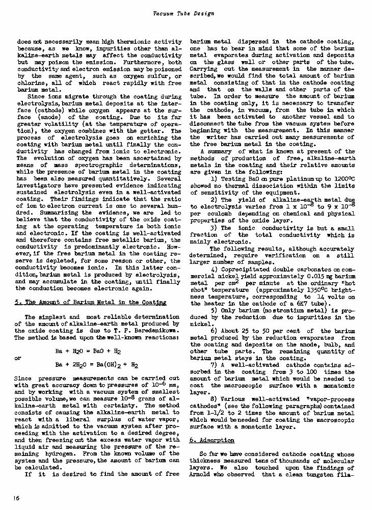
The simplest and most reliable determinationof the amount of alkaline -earth metal produced bythe oxide coating is due to T. P. Beredenikowa.The method is based upon the well-known reactions:
orBa + H2O = Ba0 + H2
Ba + 2H20 = Ba(OH)2 + H2
Since pressure measurements can be carried outwith great accuracy down to pressures of 10-6 mm,and by working with a vacuum system of smallestpossible volume,we can measure 10-8 grams of al-kaline -earth metal with certainty. The methodconsists of causing the alkaline -earth metal toreact with a liberal surplus of water vapor,which is admitted to the vacuum system after pro-ceeding with the activation to a desired degree,and then freezing out the excess water vapor withliquid air and measuring the pressure of the re-maining hydrogen. From the known volume of thesystem and the pressure, the amount of barium canbe calculated.
If it is desired to find the amount of free
barium metal dispersed in the cathode coating,one has to bear in mind that some of the bariummetal evaporates during activation and depositson the glass wall or other parts of the tube.
Carrying out the measurement in the manner de-scribed, we would find the total amount of bariummetal consisting of that in the cathode coatingand that on the walls and other parts of thetube. In order to measure the amount of bariumin the coating only, it is necessary to transferthe cathode, in vacuum, from the tube in whichit has been activated to another vessel and todisconnect the tube from the vacuum system beforebeginning with the measurement. In this mannerthe writer has carried out many measurements ofthe free barium metal in the coating.
A summary of what is known at present of themethods of production of free, alkaline -earthmetals in the coating and their relative amountsare given in the following:
1) Testing BaOmpure platinum up to 1200°Cshowed no thermal dissociation within the limitsof sensitivity of the equipment.
2) The yield of alkaline -earth metal duto electrolysis varies from 1 x 10⁻⁸ to 9 x 10-°per coulomb depending on chemical and physicalproperties of the oxide layer.
3) The ionic conductivity is but a smallfraction of the total conductivity which ismainly electronic.
The following results, although accuratelydetermined, require verification on a stilllarger number of samples.
4) Coprecipitated double carbonates on com-mercial nickel yield approximately 0.015 mg bariummetal per cm2 per minute at the ordinary "hotshot" temperature (approximately 1350°C bright-ness temperature, corresponding to 14 volts onthe heater in the cathode of a 6K7 tube).
5) Only barium (no strontium metal) is pro-duced by the reduction due to impurities in thenickel.
6) About 25 to 50 per cent of the bariummetal produced by the reduction evaporates fromthe coating and deposits on the anode, bulb, andother tube parts. The remaining quantity ofbarium metal stays in the coating.
7) A well -activated cathode contains ad-sorbed in the coating from 3 to 100 times theamount of barium metal which would be needed tocoat the macroscopic surface with a monatomiclayer.
8) Various well -activated "vapor -processcathodes" (see the following paragraphs) containedfrom 1-1/2 to 2 times the amount of barium metalwhich would be needed for coating the macroscopicsurface with a monatomic layer.
6. Adsorption
So far we have considered cathode coating whosethickness measured tens of thousands of molecularlayers. We also touched upon the findings ofArnold who observed that a clean tungsten fila-
16
Lederer: Filaments and Cathodes -- Part II
meat, arranged near an oxide -coated cathode, be-comes emissive although no visible change of thetungsten surface can be detected. We know nowthat the thermionic activity of Arnold's tung-sten filament is due to the adsorption of bariummetal and since such effects are of great im-portance, both technically and commercially, a
short discussion of the fundamentals may be inorder.
We are accustomed to regard an atom as com-posed of a nucleus surrounded by a number ofelectrons revolving about the nucleus in definiteorbits. If we remove a negative quantity, anelectron, from the atom, which as such is un-charged, a positively charged body, called a
positive ion, remains. We know that we can re-move only the outermost electrons which areloosely bound to the atom. If an atom becomesadsorbed on a metiolic surface and no change inthe number of its electrons takes place, we speakof an adsorbed atom or adatom. If one of the
electrons becomes associated with the atoms ofthe metal, the atom is changed to an ion and
since it is adsorbed we speak of an adion. It
is also conceivable that the adatom shares one
electron with the metal in which case it maychange its identity from adatom to adion and backabout 1016 times per second. We believe thishappens in view of recent computations. Metalatoms which have a low work function (or lowionizing potential in the vapor state) lose theirvalency electrons in relatively weak fields. Ifsuch metal atoms, for example, caesium or barium,become adsorbed on a metal with high work func-tion, such as tungsten, the adsorbed film con-sists of adatoms and adions. Thus, the adsorbedfilm which must be not more than one atom deep,possesses properties which are not common to theadsorbed metal in bulk.
Let us consider a condenser whose plates Cand A are made of tungsten, and short-circuitedby a tungsten wire, as shown in Fig. 11. If we
introduce a positively charged grid G between
C GX
X
X
A
Fig. 11
the two condenser plates, fields are producedbetween C and G, and between G and A. Also,there will be a potential difference betweenC and G and an equal potential difference betweenG and A. Moving G closer to C causes the fieldbetween C and G to grow stronger. If we imaginethe grid to consist of atoms and positive ions
one atomic distance away from C, we have a pic-ture of adatoms and adions and the fields theyproduce. Opening the electrical connection be-tween both plates causes the adsorbed film tomanifest itself by causing a contact potentialdifference and, because of the strong field be-tween C and G, the film aids the egress of elec-trons from C, i.e., it lowers the work functionof C.
The reduction in work function due to ad-sorbed ions has been computed by J. A. Becker.He has made certain simplifying assumptions andhas supposed that the physical dimensions ofadions and adatoms are equal to their dimensionsderived from X-ray data. Comparing computationand experimental data, Becker concluded that onthe average 10 per cent of the adsorbed particlesare ionized. We must bear in mind that due tostrong assymetric forces adatoms and adions mustbe distorted and are, therefore, different fromthose in free space. The distortion must havesome effect upon the work function. A superficialcorrelation between work function and atomic vol-ume has been pointed out by Schottky, Langmuir,and Cushman. While we know that monatomic filmsarrange themselves in conformity with the under-lying lattice, it must be admitted that we do notpossess sufficient information to compute the de-crease of the work function due to adsorbed par-ticles. Finally, when we deal with the magnitudeof surfaces in evaluating experimental results,great errors may occur. Bowden and Rideal mea-sured the ratio between actual and apparent sur-faces. If this ratio Is unity for polished nickel,it is about 10 for sandblasted nickel, and 45for oxidized and reduced nickel. The measure-ments of the writer pertaining to the bariumcontent of vapor -process cathodes were carriedout with polished surfaces.
The difference in thermionic activity betweenmonatomic layers of barium and barium in bulkcan be seen qualitatively from a diagram in Fig.12 by Ryde and Harries. They measured emission,as a function of time, from a tungsten filament
s
TIME
Fig. 12
on which barium metal was allowed to condense.The evaporation of barium onto the filament couldbe stopped at will.
17
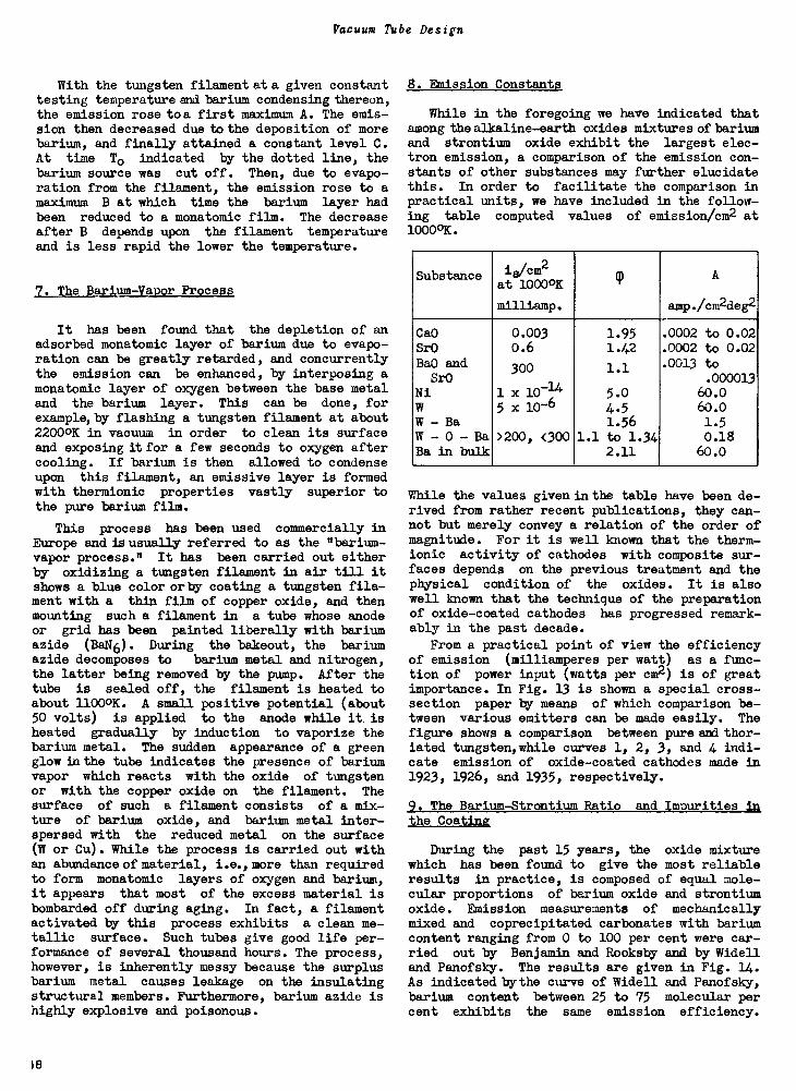
Vacuum Tube Design
With the tungsten filament at a given constanttesting temperature and barium condensing thereon,the emission rose toa first maximum A. The emis-sion then decreased due to the deposition of morebarium, and finally attained a constant level C.At time To indicated by the dotted line, thebarium source was cut off. Then, due to evapo-ration from the filament, the emission rose to amaximum B at which time the barium layer hadbeen reduced to a monatomic film. The decreaseafter B depends upon the filament temperatureand is less rapid the lower the temperature.
7. The Barium -Vapor Process
It has been found that the depletion of anadsorbed monatomic layer of barium due to evapo-ration can be greatly retarded, and concurrentlythe emission can be enhanced, by interposing amonatomic layer of oxygen between the base metaland the barium layer. This can be done, forexample, by flashing a tungsten filament at about22000K in vacuum in order to clean its surfaceand exposing it for a few seconds to oxygen aftercooling. If barium is then allowed to condenseupon this filament, an emissive layer is formedwith thermionic properties vastly superior tothe pure barium film.
This process has been used commercially inEurope and isusunily referred to as the "barium -vapor process." It has been carried out eitherby oxidizing a tungsten filament in air till itshows a blue color or by coating a tungsten fila-ment with a thin film of copper oxide, and thenmounting such a filament in a tube whose anodeor grid has been painted liberally with bariumazide (BaN6). During the bakeout, the bariumazide decomposes to barium metal and nitrogen,the latter being removed by the pump. After thetube is sealed off, the filament is heated toabout 11000K. A small positive potential (about50 volts) is applied to the anode while it. isheated gradnAlly by induction to vaporize thebarium metal. The sudden appearance of a greenglow lathe tube indicates the presence of bariumvapor which reacts with the oxide of tungstenor with the copper oxide on the filament. Thesurface of such a filament consists of a mix-ture of barium oxide, and barium metal inter-spersed with the reduced metal on the surface(w or Cu). While the process is carried out withan abundance of material, i.e., more than requiredto form monatomic layers of oxygen and barium,it appears that most of the excess material isbombarded off during aging. In fact, a filamentactivated by this process exhibits a clean me-tallic surface. Such tubes give good life per-formance of several thousand hours. The process,however, is inherently messy because the surplusbarium metal causes leakage on the insulatingstructural members. Furthermore, barium azide ishighly explosive and poisonous.
8. Emission Constants
While in the foregoing we have indicated thatamong the alkaline -earth oxides mixtures of bariumand strontium oxide exhibit the largest elec-tron emission, a comparison of the emission con-stants of other substances may further elucidatethis. In order to facilitate the comparison inpractical units, we have included in the follow-ing table computed values of emission/cm2 at1000°K.
Substance is/cm2at 10000K
milliamp.
(1)A
amp./cm2deg2
Ca0 0.003 1.95 .0002 to 0.02Sr0 0.6 1.42 .0002 to 0.02Ba0 and 300 1.1 .0013 to
Sr° .000013
Ni 1 x 10-14 5.0 60.0
W 5 x 10⁻⁶ 4.5 60.0W - Ba 1.56 1.5W - 0 - Ba >200, <300 1.1 to 1.34 0.18Ba in bulk 2.11 60.0
While the values given lathe tablerived from rather recent publications, they can-not but merely convey a relation of the order ofmagnitude. For it is well known that the therm -ionic activity of cathodes with composite sur-faces depends on the previous treatment and thephysical condition of the oxides. It is alsowell known that the technique of the preparationof oxide -coated cathodes has progressed remark-ably in the past decade.
From a practical point of view the efficiencyof emission (milliamperes per watt) as a func-tion of power input (watts per cm2) is of greatimportance. In Fig. 13 is shown a special cross-section paper by means of which comparison be-tween various emitters can be made easily. Thefigure shows a comparison between pure and thor-iated tungsten,while curves 1, 2, 3, and 4 indi-cate emission of oxide -coated cathodes made in1923, 1926, and 1935, respectively.
have been de -
9. The Barium -Strontium Ratio and Impurities itkthe Coating
During the past 15 years, the oxide mixturewhich has been found to give the most reliableresults in practice, is composed of equal mole-cular proportions of barium oxide and strontiumoxide. Emission measurements of mechanicallymixed and coprecipitated carbonates with bariumcontent ranging from 0 to 100 per cent were car-ried out by Benjamin and Rooksby and by Widelland Panofsky. The results are given in Fig. 14.As indicated by the curve of Widell and Panofsky,barium content between 25 to 75 molecular percent exhibits the same emission efficiency.
18
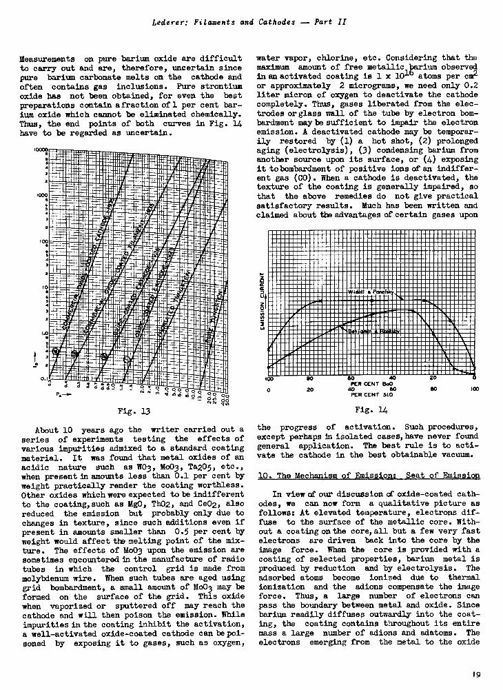
Lederer: Filaments and Cathodes -- Part II
Measurements on pure barium oxide are difficultto carry out and are, therefore, uncertain sincepure barium carbonate melts on the cathode andoften contains gas inclusions. Pure strontiumoxide has not been obtained, for even the bestpreparations contain afractionofl per cent bar-ium oxide which cannot be eliminated chemically.Thus, the end points of both curves in Fig. 14have to be regarded as uncertain.
10000
6 iralkageMiliMPAHM16"41:2-1...a
4 Hinninin 1111:11111F nil 1111391;11111:1iIir;
fLIIIII:iiiirdp=1331 .1.2441_Erminduapririi...........anur-unifi,---.. . ....np.r..v..15--rliair,simmalmenpm,epc.mogran
eporamIraMilihiiiLfirallii.noINNERIONIIIIIIII4 ArimuluirritaaranniniaiNIVINMalijarnarviisaWirmealwassriliairdinVr
inimairgallinf*iriandrarlAnillifiiniiiill&INNin
wahinimumeirmlINENINIALinvIIINIMINIWILINIENSME----7:1"10M10-E67741NVIN9IPPEzzlimourfordzilwtaaararraidomn
muieripanunnomulikureanagwounill
, 0
aridaVNIET:hWiANIMIL9.1.1.144ii
.......cummanu:immustrA!mItAlloingamil*zuLtain" meth digital
tliumm.misim..:.....,.A.......,
421ri.141fintraiffitrardkitillropOIN1.01
IlMilikiiiiiiiiii'sa rtairmiwununmeM,... el.2. arimmovinumnimuran ;-,1M161
0 riaru +71:11174:74TINificinizni I frelr.Sic:Monorioil
11 Ido : :N M g ol/0.0.f.s2
(og,2 °
I000
4
100
4
Fig. 13
About 10 years ago the writer carried out a
series of experiments testing the effects ofvarious impurities admixed to a standard coating
material. It was found that metal oxides of anacidic nature such as W03, Mo03, Ta205, etc.,when present in amounts less than 0.1 per cent byweight practically render the coating worthless.Other oxides which were expected to be indifferentto the coating, such as MgO, Th02, and Ce02, also
reduced the emission but probably only due tochanges in texture, since such additions even ifpresent in amounts smaller than 0.5 per cent byweight would affect the melting point of the mix-ture. The effects of Mo03 upon the emission aresometimes encountered in the manufacture of radiotubes in which the control grid is made frommolybdenum wire. When such tubes are aged usinggrid bombardment, a small amount of Mo03 may be
formed on the surface of the grid. This oxide
when vaporized or sputtered off may reach thecathode and will then poison the emission. Whileimpurities in the coating inhibit the activation,a well -activated oxide -coated cathode can be poi-
soned by exposing it to gases, such as oxygen,
water vapor, chlorine, etc. Considering that themaximum amount of free metallic parium observedin an activated coating is 1 x 101' atoms per cm2or approximately 2 micrograms, we need only 0.2liter micron of oxygen to deactivate the cathodecompletely. Thus, gases liberated from the elec-trodes or glass wall of the tube by electron bom-bardment maybe sufficient to impair the electronemission. A deactivated cathode may be temporar-ily restored by (1) a hot shot, (2) prolongedaging (electrolysis), (3) condensing barium fromanother source upon its surface, or (4) exposingit to bombardment of positive ions drab indiffer-ent gas (CO). When a cathode is deactivated, thetexture of the coating is generally impaired, sothat the above remedies do not give practicalsatisfactory results. Much has been written andclaimed about the advantages of certain gases upon
ceJ
2
inn MMMMMMMMMM mum MMMMM nommonommnim MMMMM mommonnumm MMMMMMMMMMMMMMMMM moomlomomommommo MMMMMMMMM mummummoo MMMMMMMM mommm MMMMM mionommomminnionmimmummommommionommMMMMMMM mmum MMMMMMMMMMMMMMMMMM nomMMMMMmommomm MMMMMMMMMM ons MMMMMMMMMM nommonmommommiimmimmommommenommomm MMMMMMMMM MOMMEMEMEMNn n MMMMMMMMMM mom MMMMMMM mnommom MMMMMMMMM momm MMMMM nnominn MMMMMMM mime MMMMM nom MMMMM ONMENNIMMEMMMMMMMMMMMMM MEMMU MMMMM MMEMMEMBENEMMEMMEMMENNEMBEMMMEMMEMMEMMMIMMUMUMEMMEMMEMEN MMMMM 111.11111111.111.111 MMMMMS EMEMEMEMMEMIMMEMMMEME MMMMM WEEMMEMMMME MMMMM MEMMOMEMMEMEMEN MMMMM ENE MMMMMMMMMM MMEMMEMEMOMMEMMEMMMEMMMEMMEMMEMMENNEUMN MMMMMMMM EWEN MMMMMMMMMMMMMMMMM MEMUM MMMMM MallIMMOW0:306=2:2E NNEMMEMMEN MMMMMMMMMMMMMMMMMMMMMMMMMMMMM EMMEN!'IIMMEMEMMEIPM MMMMMMMMMMMMMMMMMMMMMMMMM EldigNUMEMMEMOMMIIIMMOMMMRS OIMEMMEMENMMEMEFAMMENEEM MMMMMMMMMM MASSOMMMENOWOrMOMIMEMEMMMINNA= MMMMMMMMMMM 0111111.111
MENUMM ndliaM/E20111117 ", MM MM ME
MdMEMEMMENAMMINEEMMEMMENEW MM MMMMM OEMswilimmommrsI.a
onoAmmonium MMMMMM so MMMMMMM mom MMMMMMMMMM m
on
101111 WOMMIIMMIOV
100
0
SO 60PER CENT 8.0
20 40 60PER CENT 510
Fig. 14
40 20
80 100
the progress of activation. Such procedures,except perhaps in isolated cases, have never foundgeneral application. The best rule is to acti-vate the cathode in the best obtainable vacuum.
10. The Mechanism of Emission: Seat of Emission
In view of our discussion of oxide -coated cath-
odes, we can now form a qualitative picture asfollows: At elevated temperature, electrons dif-fuse to the surface of the metallic core. With-out a coating on the core, all but a few very fastelectrons are driven back into the core by theimage force. When the core is provided with acoating of selected properties, barium metal isproduced by reduction and by electrolysis. The
adsorbed atoms become ionized due to thermalionization and the adions compensate the imageforce. Thus, a large number of electrons canpass the boundary between metal and oxide. Sincebarium readily diffuses outwardly into the coat-ing, the coating contains throughout its entiremass a large number of adions and adatoms. The
electrons emerging from the metal to the oxide
19
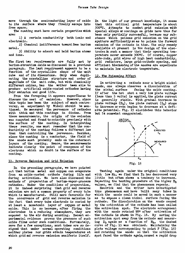
Vacuum Tube Design
move through the semiconducting layer of oxideto its surface where they finally escape intofree space.
The coating must have certain properties whichare:
1) A certain conductivity both ionic andelectronic.
2) Chemical indifference toward free bariummetal.
3) Ability to adsorb and hold barium atomsand ions.
The first two requirements are fully met bybarium -strontium oxide as discussed in a previousparagraph. The last requirement appears to be afunction of the crystalline shape of the unitcube and of its dimensions. Only when dupli-cating the crystalline structure and order ofmagnitude of the unit cube, but with chemicallydifferent oxides, has the writer been able toproduce artificial oxide -coated cathodes havingfair emission and good life.
From the foregoing it appears superfluous todiscuss the seat of emission. However, sincethis topic has been the subject of much contro-versy, an experiment by Widell should be men-tioned. He measured the perveance of cathodeswith thick and thin coatings in diodes. Fromthese measurements, the origin of the emissionwas computed and found to coincide precisely withthe surface of the coating. In interpretingthese results, one must remember that the con-ductivity of the coating follows a different lawthan that controlling the perveance. Besides,since the coating is a conductor, the field ofthe anode most probably ends on the outermostlayers of the coating. Hence, the measurementsindicate clearly the point of emergence of theelectrons which no doubt is the surface of thecoating.
11. Reverse Emission and Grid Emission
In the preceding paragraphs, we have pointedout that barium metal and oxygen can evaporatefrom an oxide -coated cathode during life andduring activation. We have also discussed themethods of preparation of barium -vapor -process
cathodes. Under the conditions of preparation,it is indeed surprising that grid and reverseemission are not a common property of every tubewhich is manufactured. Still more favorable forthe occurrence of grid and reverse emission isthe fact that every tube electrode is coated byat least a monatomic layer of oxygen or metaloxide. This is so because, after firing theelectrodes in a reducing atmosphere, they areexposed to the air during mounting. Recent ex-perimental evidence proves the presence of suchoxide films under such conditions. Fortunately,save for a few exceptions, most tubes are so de-signed that under normal operating conditionsneither plates nor grids attain temperatures atwhich grid sal reverse emission manifests itself.
In the light of our present knowledge, it seemsthat this critical grid temperature is about300°C. Attempts to combat grid emission withspecial alloys or coatings on grids have thus farbeen only partially successful, because any sub-stance which poisons grid emission on the gridsputters sufficiently so as to poison the forwardemission of the cathode in time. The only remedyavailable at present is the design of the elec-trodesin such a manner that their operating tem-perature never exceeds 3000C. Of course, copperside -rods, grid wires of high heat conductivity,grid radiators, large grid -cathode spacing, andefficient blackening of the anodes are expedientsto maintain low electrode temperature.
12. The Poisoning Effect
In activating a cathode near a bright nickelanode, one always observes a discoloration ofthe nickel surface facing the oxide coating.If after the hot shot a very low plate voltage(less than 5 volts) is applied, the plate currentis generally stable. With gradual increase inplate voltage (Eb), the plate current (Ib) stopsto increase or even begins to decrease at a defi-nite potential. Fig. 15 elucidates this behaviorbut is somewhat exaggerated.
Ib
CRITICALPOTENTIAL
\\I Ar
P /.....
EXPECTEDI
/ I Ib/ II / 1I/
MEASUREDI
Eb
Fig. 15
Testing again under the original conditionswith low Eb, we find that Ib has decreased verylittle but often shows a tendency to increase.Repeating the testing procedure at the higher Ebvalues, we find that the phenomenon repeats.
Headrick and the writer have investigatedthis phenomenon and have built many tubes inwhich the anode could be moved in such a manneras to expose a clean nickel surface facing thecathode. The discoloration on the anode causedby the activation of the cathode has been calledthe activation spot. The electrode arrangementwith the anode rotated 900 after activation ofthe cathode is shown in Fig. 16. By moving theactivation spot away from the cathode and measur-ing Ib again as a function of Eb, the dashedcurve of Fig. 15 was obtained. Maintaining theplate voltage corresponding to point P (Fig. 15)and rotating the anode so that the activationspot faced the cathode again, caused a rapid drop
20
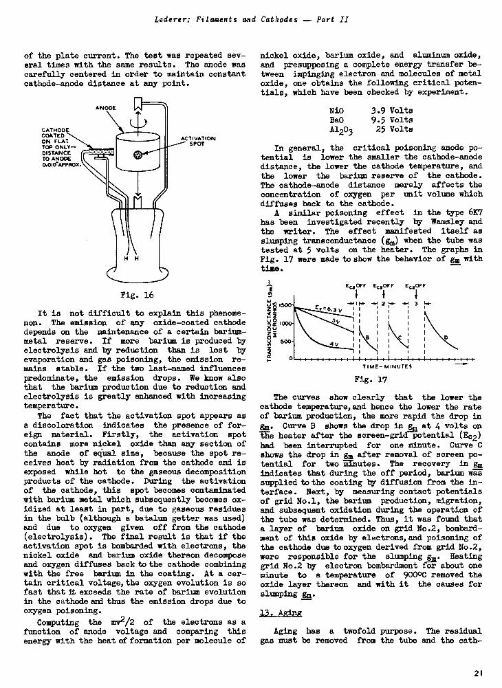
Lederer: Filaments and Cathodes -- Part II
of the plate current. The test was repeated sev-eral times with the same results. The anode wascarefully centered in order to maintain constantcathode -anode distance at any point.
ANODE
CATHODCOATEDON FLATTOP ONLY-DISTANCETO ANODE0.010`APPROX.
Fig. 16
ACTIVATIONSPOT
It is not difficult to explain this phenome-non. The emission of any oxide -coated cathodedepends on the maintenance of a certain barium -metal reserve. If more barium is produced byelectrolysis and by reduction than is lost byevaporation and gas poisoning, the emission re-mains stable. If the two last-named influencespredominate, the emission drops. We know alsothat the barium production due to reduction andelectrolysis is greatly enhanced with increasingtemperature.
The fact that the activation spot appears asa discoloration indicates the presence of for-eign material. Firstly, the activation spotcontains more nickel oxide than any section ofthe anode of equal size, because the spot re-ceives heat by radiation from the cathode and isexposed while hot to the gaseous decompositionproducts of the cathode. During the activationof the cathode, this spot becomes contaminatedwith barium metal which subsequently becomes ox-idized at least in part, due to gaseous residuesin the bulb (although a batalum getter was used)and due to oxygen given off from the cathode(electrolysis). The final result is that if theactivation spot is bombarded with electrons, thenickel oxide and barium oxide thereon decomposeand oxygen diffuses back to the cathode combiningwith the free barium in the coating. At a cer-tain critical voltage, the oxygen evolution is sofast that it exceeds the rate of barium evolutionin the cathode and thus the emission drops due tooxygen poisoning.
Computing the mv2/2 of the electrons as afunction of anode voltage and comparing thisenergy with the heat of formation per molecule of
nickel oxide, barium oxide, and aluminum oxide,
and presupposing a complete energy transfer be-tween impinging electron and molecules of metaloxide, one obtains the following critical poten-tials, which have been checked by experiment.
Ni0Ba0A1203
3.9 Volts9.5 Volts25 Volts
In general, the critical poisoning anode po-tential is lower the smaller the cathode -anodedistance, the lower the cathode temperature, andthe lower the barium reserve of the cathode.
The cathode -anode distance merely affects the
concentration of oxygen per unit volume whichdiffuses back to the cathode.
A similar poisoning effect in the type 6E7has been investigated recently by Wamsley andthe writer. The effect manifested itself asslumping transconductance (gm) when the tube wastested at 5 volts on the heater. The graphs inFig. 17 were made to show the behavior of gm withtime.
Zen 1500
g0000Z0
500zcc
EcaOFF
-.4 3
TIME- MINUTES
Fig. 17
The curves show clearly that the lower thecathode temperature, and hence the lower the rateof barium production, the more rapid the drop ingm. Curve B shows the drop in §A at 4 volts onEEe heater after the screen -grid potential (Ec2)
had been interrupted for one minute. Curve Cshows the drop in gm after removal of screen po-tential for two minutes. The recovery in gmindicates that during the off period, barium wassupplied to the coating by diffusion from the in-terface. Next, by measuring contact potentialsof grid No.1, the barium production, migration,and subsequent oxidation during the operation ofthe tube was determined. Thus, it was found thata layer of barium oxide on grid No.2, bombard-ment of this oxide by electrons, and poisoning ofthe cathode due to oxygen derived from grid No.2,were responsible for the slumping g. Heatinggrid No.2 by electron bombardment for about oneminute to a temperature of 9000C removed theoxide layer thereon and with it the causes forslumping gm.
13. Aging
Aging has a twofold purpose. The residualgas must be removed from the tube and the cath-
2 I
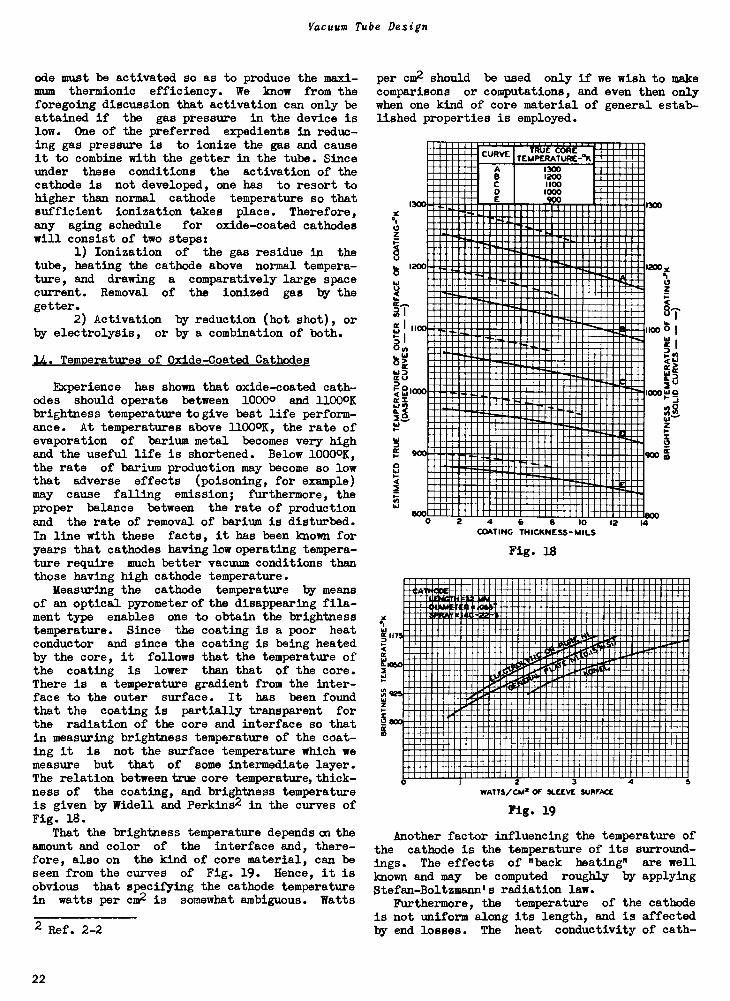
Vacuum Tube Design
ode must be activated so as to produce the maxi-mum thermionic efficiency. We know from theforegoing discussion that activation can only beattained if the gas pressure in the device islow. One of the preferred expedients in reduc-ing gas pressure is to ionize the gas and causeit to combine with the getter in the tube. Sinceunder these conditions the activation of thecathode is not developed, one has to resort tohigher than normal cathode temperature so thatsufficient ionization takes place. Therefore,any aging schedule for oxide -coated cathodeswill consist of two steps:
1) Ionization of the gas residue in thetube, heating the cathode above normal tempera-ture, and drawing a comparatively large spacecurrent. Removal of the ionized gas by thegetter.
2) Activation by reduction (hot shot), orby electrolysis, or by a combination of both.
14. Temperatures of Oxide -Coated Cathodes
Experience has shown that oxide -coated cath-odes should operate between 10000 and 11000Kbrightness temperature to give best life perform-ance. At temperatures above 11000K, the rate ofevaporation of barium metal becomes very highand the useful life is shortened. Below 10000K,the rate of barium production may become so lowthat adverse effects (poisoning, for example)may cause falling emission; furthermore, theproper balance between the rate of productionand the rate of removal of barium is disturbed.In line with these facts, it has been known foryears that cathodes having low operating tempera-ture require much better vacuum conditions thanthose having high cathode temperature.
Measuring the cathode temperature by meansof an optical pyrometer of the disappearing fila-ment type enables one to obtain the brightnesstemperature. Since the coating is a poor heatconductor and since the coating is being heatedby the core, it follows that the temperature ofthe coating is lower than that of the core.There is a temperature gradient from the inter-face to the outer surface. It has been foundthat the coating is partially transparent forthe radiation of the core and interface so thatin measuring brightness temperature of the coat-ing it is not the surface temperature which wemeasure but that of some intermediate layer.The relation between true core temperature, thick-ness of the coating, and brightness temperatureis given by Widell and Perkins2 in the curves ofFig. 18.
That the brightness temperature dependsootheamount and color of the interface and, there-fore, also on the kind of core material, can beseen from the curves of Fig. 19. Hence, it isobvious that specifying the cathode temperaturein watts per cm2 is somewhat ambiguous. Watts
2 Ref. 2-2
per cm2 should be used only if we wish to makecomparisons or computations, and even then onlywhen one kind of core material of general estab-lished properties is employed.
1
0
CURVE
A
C
E
TRUE CORETEMPERATURE -'K
1300
1100200
000900
"wampum mmmmmmmmmmm m mmmmmmmmmmm IMMOMOIMMMIKE mmmmmmmm MOM mmmmmmmm MMMMM
= MMMMMMM MEMO MMMMMMMEMMOOMM MMMMMMMMM MMMMM MMOMMMEMME
t 1200
=
El,
II8061>
MM to
°1000
0
20
800
7
mu.=mmilimminmaft.8 MMMMMM mu MMMMMMM osommemmimmummimmimmbammum MMMMMMM mism.....mmosmomm MMMMMM Ems
Ivo MMMMMMM MEMEISZKETMEMMOMEG=NNIMOMM MMMMMMM MOMMMII.TAIVIMMEMMOMMOMMOMMIllae4MOMM MMMMM Mommon6a.m8MMEMMEMEMMOMIIMMIBMTMOIMMEMMEMMOMMIOnliaMMiaMMEMMIUMMEMMINIMIDCEMMOMMEMMEMMOMMMMEMORmi=m11111MMOMMEMMEMMOMMEMMMOMMOMOSOMMEMEMMUmi:MMOMMOMMEMMINOMMIIMMEMEMMEMMEMOMMEMMEMMO6=FOIMMOMMIIMEMMMEMSMMIMMOMMEMMEMMOMMMEMSft=5111MMIMMOMEMM
..EMMOMEMMOMMOMMEMMOMMOMMOMb.NOMMIMMEMMMMM MMEMOMMEMMINIMEMEMEN=.11MM
11111811MIWGZMOMMEMMINMEMMOMMINMMOU:2MEMMOMMIIMOMMMECTIPREMMIIMMIMMOMMEMMOMMMMMM mmlimmommimmhamimmimimmmonlIMmiummam!emommillimimmillinimmomillimmmonmilimummonsiAzmmommolimmmummummilMEmmumms MMMMM mommemozmammmilmmummommMOM MMMMM OMMEMOMMIIMMEW.7.91 MMMMMIIMMOMMIIMMOMMINEMMMEMMEMMEMMaZMILMIMMOMMIIMMOMMEMIUMOMMOMMO MMMMM mommmam9
m MMMMM MIMIMMEMOMMOMMEMMOMMEMMINSMEMMMOMMO.21=PMEMMIIMMEMMEMMEMMMINIM MMMMM MEMEMMIIIIMMINW MMMMM MMOMMIIMOMMEmiliMmemom=mmilimimmmulliniammummmli011milmilliammimimmogr.MummmimmomimmimmMEMEMMOOMMEMNIMMOMMINIMmiZZFMMEMUMMEMOSMEMMOMMOMMIIMMOMMEMMEMMOMMii=m111.110111MEMMOMMOMMMOMMEMMOMMMOSEMEMOMMINftZFINIIIMMOMMOMMEMMIMMEMMOMMEMOMMEMEMOOMM
. MMEMMINIMMOMMOOMMEMWOMMEMOMMEMEMMOMMMEMbillmEMC=VIOMMMISMEMOMMEMIIMMEMMEMMMINUMMOMMEMMOUbliCIMMEMEMOMMMEMMIIMMEMMINImmii=r MMMMM OMMOMEMMOMMEMMOMMEMMMEMMIIMMMOMMEMEIKaiTEIMEMEMMOMMEMMINO
MMMMM mimmensmmommzmnmummliimmMMMMMMMMMM moms= MMMMM MION:1=T4111MEMOIMMEMMOMMEMOMMUMMEMOMEMINNOMMMEN
MMUMMOOMME MMMMM OMOMMEMMEMOMMEMMEMOMOMMEMMOMMEMMEMOMMEMMEMMOMMEMMOIMMOMMOMMOMMEMMOMM MMMMM MEMMEMMMENIMMOOMMEM:"
1300
4 6 8 10 12
COATING THICKNESS -MILS
Fig. 18
1200
0z
d.t<
1100 0
E l1- 0)
Wcr.,(>
asiC00 w 0
a2z
MMMMMMMMMMMM MOMOMMOMMEMIIIL 41=MMOMPW-.111:1
1I1Et'7ir"3-mminr.ivaats!srAal
1.-111110.1
Z.iiMIP!,s..V.'elPiO, m
MMMMMMMMMMMMMMM OMMEMIBMTVP ml,Akamprip...
.PR-twmp,111, _,r;.007momr_.
mos MMMMMMM INIMOMMITin!iMP:- 11LaMMP-.driaim..,,i1OP5,T,:noMMIti
glintalin, M
ramon.
orwmgMnINIMMEin
-111MISMI
111
IOURN
. 111
88881 IMMII2 3
wATTs/ cm2 OF SLEEVE SURFACE
Ell
Fig. 19
Another factor influencing the temperature ofthe cathode is the temperature of its surround-ings. The effects of "back heating" are wellknown and may be computed roughly by applyingStefan-Boltzmannts radiation law.
Furthermore, the temperature of the cathodeis not uniform along its length, and is affectedby end losses. The heat conductivity of cath-
22
Lederer: Filaments and Cathodes -- Part II
ode tabs, the thermal contact between cathode andmica or the filament supports, as well as thedesign of the heaters in indirectly heated cath-odes play an important role.
For the design of indirectly heated cathodes,the ratio of the thermal emissivity of the coatedto bare -core material is of importance. Withthe improvement of the technique in the manufac-ture of oxide -coated cathodes, this ratio mustbe redetermined frequently. A recent determina-tion by Widen shows this ratio to be 1.6 forthe present stage of technique. The spectralemissivity of an oxide -coated cathode(for averageconditions) has also been determined by Widelland found to be about 0.56 at X. 0.665µ
15. Calculation of Oxide -Coated Filaments
Generally, the electrical constants of a tubeare set by convention. For example, the fila-ment voltage and current have to meet certainspecifications. From the desired value of gmthe filament -grid spacing, and other mechanicTIconsiderations, we can determine the length ofthe filament. Thus, we have
Filament length = LFilament voltage = EfFilament current = If
We also know the desired operating temperatureto maintain good emission life which is approxi-mately 10500K or 3.2 watts per cm2 = D, and thespecific resistance p of the core material atthe operating temperature.
We wish to know the width (w) and the thick-ness (t) of a filament which having a length (L)and operating at Ef x If watts input attains atemperature of 10500K. To solve for the two un-knowns, w and t, we need two equations. Theseare:
EfIf
2(w
R =
+ t) L= D
p L = Ef
w t If
On substituting we get:
VI =
t =
EfIf +V(EfIf)24LD 4LD
EfIf /(EfIf )24LD 4LD
p L
p L
In these equations, dimensions are to be ex-pressed in centimeters and electrical values involts, amperes, and ohms.
REFERENCES
O. W. Richardson, "Emission of Electricity fromHot Bodies." (Second Edition) Longmans, Green &Company, London, 1921.
L. A. Reiman, "Thermionic Emission." John Wileyand Sons, New York, 1934.
S. Dushman, "Thermionic Emission," Review of Mod-ern Physics, Vol. 2, No.4; 1930.
K. T. Compton and I. Langmuir, "Electrical Dis-charges of Gases," Part I, Review of Modern Phys-ics, Vol. 2, No.2; 1930.
V. K. Darrow, "Statistical Theories of Matter,Radiation and Electricity." Bell Telephone Lab-oratories Reprint B-435; 1929.
P. W. Bridgeman, "Thermodynamics of ElectricalPhenomena in Metals." The Macmillan Company,New York, 1934.
J. H. DeBoer, "Electron Emission and AdsorptionPhenomena." The Macmillan Company, New York,1934.
L. R. Koller, "The Physics of Electron Tubes."McGraw-Hill Book Co., New York, 1934.
23
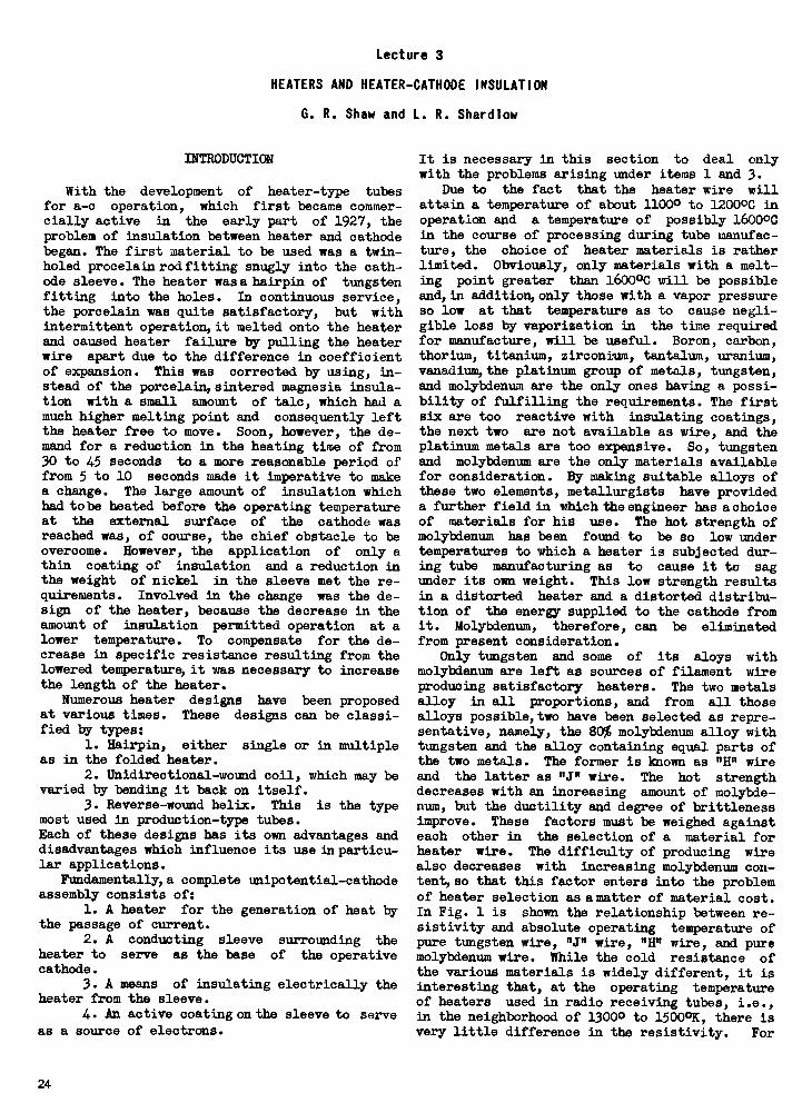
Lecture 3
HEATERS AND HEATER -CATHODE INSULATION
G. R. Shaw and L. R. Shardlow
INTRODUCTION
With the development of heater -type tubesfor a -c operation, which first became commer-cially active in the early part of 1927, theproblem of insulation between heater and cathodebegan. The first material to be used was a twin -holed procelain rod fitting snugly into the cath-ode sleeve. The heater was a hairpin of tungstenfitting into the holes. In continuous service,the porcelain was quite satisfactory, but withintermittent operation, it melted onto the heaterand caused heater failure by pulling the heaterwire apart due to the difference in coefficientof expansion. This was corrected by using, in-stead of the porcelain,sintered magnesia insula-tion with a small amount of talc, which had amuch higher melting point and consequently leftthe heater free to move. Soon, however, the de-mand for a reduction in the heating time of from30 to 45 seconds to a more reasonable period offrom 5 to 10 seconds made it imperative to makea change. The large amount of insulation whichhad tobe heated before the operating temperatureat the external surface of the cathode wasreached was, of course, the chief obstacle to beovercome. However, the application of only athin coating of insulation and a reduction inthe weight of nickel in the sleeve met the re-quirements. Involved in the change was the de-sign of the heater, because the decrease in theamount of insulation permitted operation at alower temperature. To compensate for the de-crease in specific resistance resulting from thelowered temperature, it was necessary to increasethe length of the heater.
Numerous heater designs have been proposedat various times. These designs can be classi-fied by types:
1. Hairpin, either single or in multipleas in the folded heater.
2. Unidirectional -wound coil, which may bevaried by bending it back on itself.
3. Reverse -wound helix. This is the typemost used in production -type tubes.Each of these designs has its own advantages anddisadvantages which influence its use in particu-lar applications.
Fundamentally, a complete unipotential-cathodeassembly consists of:
1. A heater for the generation of heat bythe passage of current.
2. A conducting sleeve surrounding theheater to serve as the base of the operativecathode.
3. A means of insulating electrically theheater from the sleeve.
4. An active coating on the sleeve to serve
as a source of electrons.
It is necessary in this section to deal onlywith the problems arising under items 1 and 3.
Due to the fact that the heater wire willattain a temperature of about 11000 to 12000C inoperation and a temperature of possibly 16000Cin the course of processing during tube manufac-ture, the choice of heater materials is ratherlimited. Obviously, only materials with a melt-ing point greater than 16000C will be possibleand, in addition, only those with a vapor pressureso low at that temperature as to cause negli-gible loss by vaporization in the time requiredfor manufacture, will be useful. Boron, carbon,thorium, titanium, zirconium, tantalum, uranium,vanadium, the platinum group of metals, tungsten,and molybdenum are the only ones having a possi-bility of fulfilling the requirements. The firstsix are too reactive with insulating coatings,the next two are not available as wire, and theplatinum metals are too expensive. So, tungstenand molybdenum are the only materials availablefor consideration. By making suitable alloys ofthese two elements, metallurgists have provideda further field, in which the engineer has achoiceof materials for his use. The hot strength ofmolybdenum has been found to be so low undertemperatures to which a heater is subjected dur-ing tube manufacturing as to cause it to sagunder its own weight. This low strength resultsin a distorted heater and a distorted distribu-tion of the energy supplied to the cathode fromit. Molybdenum, therefore, can be eliminatedfrom present consideration.
Only tungsten and some of its aloys withmolybdenum are left as sources of filament wireproducing satisfactory heaters. The two metalsalloy in all proportions, and from all thosealloys possible, two have been selected as repre-sentative, namely, the 80% molybdenum alloy withtungsten and the alloy containing equal parts ofthe two metals. The former is known as "H" wireand the latter as "J" wire. The hot strengthdecreases with an increasing amount of molybde-num, but the ductility and degree of brittlenessimprove. These factors must be weighed againsteach other in the selection of a material forheater wire. The difficulty of producing wirealso decreases with increasing molybdenum con-tent, so that this factor enters into the problemof heater selection as a matter of material cost.In Fig. 1 is shown the relationship between re-sistivity and absolute operating temperature ofpure tungsten wire, "J" wire, "H" wire, and puremolybdenum wire. While the cold resistance ofthe various materials is widely different, it isinteresting that, at the operating temperatureof heaters used in radio receiving tubes, i.e.,in the neighborhood of 13000 to 1500°K, there isvery little difference in the resistivity. For
24
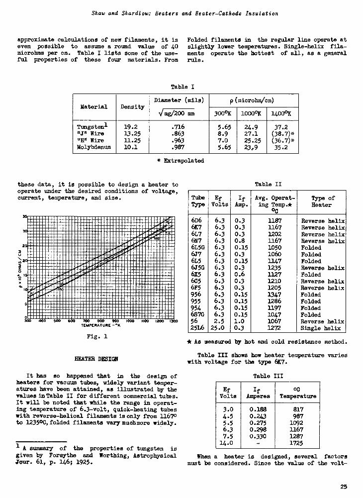
Shaw and Shardlow: Heaters and Heater -Cathode Insulation
approximate calculations of new filaments, it iseven possible to assume a round value of 40microhms per cm. Table I lists some of the use-ful properties of these four materials. From
Folded filaments in the regular line operate atslightly lower temperatures. Single -helix fila-ments operate the hottest of all, as a generalrule.
Table I
Material DensityDiameter (mils) p(microhm/cm)
N/mg/200 mm 300°K 1000°K 1400°K
Tungsten' 19.2 .716 5.65 24.9 37.2"J" Wire 13.25 .863 8.9 27.1 (38.7)*"H" Wire 11.25 .963 7.0 25.25 (36.7)*Molybdenum 10.1 .987 5.65 23..9 35.2
* Extrapolated
these data, it is possible to design a heater tooperate under the desired conditions of voltage,current, temperature, and size.
35
30
22
\200
0se 15
0
5
0300
MO
400 500 600 700 800 900TEMPERATURE -*K
Fig. 1
HEATER DESIGN
1000 1100 1200 1300
It has so happened that in the design ofheaters for vacuum tubes, widely variant temper-atures have been attained, as illustrated by thevalues in Table II for different commercial tubes.It will be noted that while the range in operat-ing temperature of 6.3 -volt, quick -heating tubeswith reverse -helical filaments is only from 1167°to 1235°C, folded filaments vary muchmore widely.
1 A summary of the properties of tungsten is
given by Forsythe and Worthing, AstrophysicalJour. 61, p. 146; 1925.
Table II
TubeType
EfVolts
IfAmp.
Avg. Operat-ing Temp.*
oc
Type ofHeater
6D6 6.3 0.3 1187 Reverse helix6K7 6.3 0.3 1167 Reverse helix6L7 6.3 0.3 1202 Reverse helix6N7 6.3 0.8 1167 Reverse helix6L5G 6.3 0.15 1050 Folded6J7 6.3 0.3 1060 Folded6L5 6.3 0.15 1147 Folded6J5G 6.3 0.3 1235 Reverse helix6X5 6.3 0.6 1127 Folded6C5 6.3 0.3 1210 Reverse helix6F5 6.3 0.3 1205 Reverse helix956 6.3 0.15 1347 Folded955 6.3 0.15 1286 Folded954 6.3 0.15 1197 Folded6S7G 6.3 0.15 1047 Folded56 2.5 1.0 1067 Reverse helix25L6 25.0 0.3 1272 Single helix
* As measured by hot and cold resistance method.
Table III shows how heater temperaturewith voltage for the type 6K7.
Table III
EfVolts
IfAmperes
OC
Temperature
3.0 0.188 817
4.5 0.243 9875.5 0.275 10926.3 0.298 11677.5 0.330 1287
14.0 - 1725
varies
When a heater is designed, several factorsmust be considered. Since the value of the volt -
25

Vacuum Tube Design
age E and the currentoperating temperaturespecific resistance p
I is set, together with theT, which determines the, we have
E 4 p S
I n d2
where S = length of wire for heater.Unfortunately, we are dealing with energy
transfer by both radiation and conduction and nowell-defined formula can be given for the rateof transfer of energy from heater to cathodesleeve. This is further complicated by the factthat the geometrical shape of the heater is nota simple one in practice, and so calculation isdifficult. In addition, neither the radiatingcharacteristics of the coated heater, as affectedby thickness of coating, type of spray, and shape,nor the reflecting properties of the inner sur-face of the nickel sleeve are known. Conse-quently, this leads to the method of designingthe heater by successive approximations to obtainthe desired current, voltage, and temperature.Much stress has been placed on the importance ofcorrectly designed heaters. The reason for thiswill be given later when we discuss the insula-tion phases of the subject.
Probably the easiest way to explain heaterdesign2 is by example. The following calcula-tions apply to a theoretical heater for the 6K7,and are based on the following assumed values:an operating temperature of 1360°K, which hasbeen determined by experience to fall within thetemperature "safety zone" of our insulating ma-terials, a dissipation per sq cm of wire surfaceof 5.5 watts, a current of 9.3 ampere, and aspecific resistance of 36 x 10-0 ohms/cm at theoperating temperature.
The diameter of wire is given by the equation
d=-c14 I2 p
2 n
where d is the diameter of the wire in centi-meters, I is the current in amperes, p is thespecific resistance in ohms/cmpand n is the dis-sipation in watts/cm2. Substituting numericalvalues in the equation we have
d = x .09 x .000036vV
n2 x 5.5
d = .0062 cm = .00244 inches
For purposes of illustration, we will supposethat this heater is to be made of "J" wire. Then,from Table I, we have
2 Ref: 3-2
d(ails) = .863 V1 mg/200 mm
(2.44)2= mg/200 mm
k.863
8.02 = mg/200 mm
The cut length of wire for the heater is
found from the equation
E I 6.3 x .3S - - 17.6 cm
n d n nx.0062x5.5
To determine the turns per inch (TPI) in eachhalf of the double helix of a heater made fromwire of the above specifications, we have theequation
TPI -Mr - 1
n (D + d)
where S is the length of wire for the coil in mm,L is the coil length in mm, D is the mandrel di-ameter in inches, and d is the wire diameter ininches.
Assume that we are constructing a coil for a45 -mil cathode, and that the wound length ofthe coil shall be 23 mm, using a 17 -mil mandrel,and that the leg length on the coil is 5 mm.Substituting numerical values in the above equa-tion, we have
(T)2 - 1TPI - = 57
n (.017 + .00244)
As mentioned before, the radiation charac-teristics of the coating, as affected by thick-ness, type of spray, and reflecting propertiesof the inner face of the sleeve, all affect thedesign of a heater, but they are to all intentsand purposes unknown. Consequently, the designof a heater in its final analysis becomes a ser-ies of successive approximations. However, letus compare the theoretical heater we have madefor the 6K7 with the actual heater now beingused.
Table IV
6K7 Heater Theoretical Actual
Wire J JWire diameter (mils) 2.44 2.46Wire weight (mg) 8.02 7.94 to 8.26Wire length (mm) 176 165TPI 57 58Operating temp. (°K) 1360 1440
26

Shaw and Shardlow: Heaters and Heater -Cathode Insulation
The next step is to take the theoreticalheater and test it in a tube to determine its
current and operating temperature. It is at thispoint that the "series of successive approxima-tions" begins. These calculations are based onOhm's law, which is E = IR.
Remembering that resistance is inversely pro-porttmmiltocross-section (which can be expressedas wire weight), other factors remaining con-stant, and that resistance is directly propor-tional to length, we can correct the theoreticalheater. For instance, it will be noticed inTable IV that the cut lengths of the theoreticaland actual heater do not agree by approximately6.5%,and that the operating temperatures are ap-proximately 800 apart. The correction in cutlength was made by the use of Ohm's law as shownabove.
INSULATING MATERIALS
The problem of insulation of heaters is adifficult one. In the automobile industry, whereceramic bodies are used as a means of insulationin spark plugs, the requirement of low conduc-tivity at high temperatures is recognized as oneof the most severe to be met with in the commer-cial field. But translated into terms of designpractice of modern radio tubes, the insulationwould not be satisfactory by a factor varyingbetween 100 and 100000, depending on the typeof tube, the temperature at which it operates,and somewhat on the method of using the tube.
It is evident that the choice of suitablematerials for insulating purposes is limited toa marked degree. The better grades of porcelainwere used at first, but their low melting points(as compared with the conditions of use), theirlow electrical resistivity, and their reactivitywith the heater wire rendered them obsolete. Thecoefficient of thermal expansion of porcelain isonly about half that of the pure oxides now gen-erally used and matches that of tungsten heatersmore closely, but, in spite of this, only thepure oxides offertheproperties which are neededfor modern tubes. Of the oxides available, onlyalumina, magnesia,beryllia, zirconia, and thoriahave a sufficiently high melting point to offerthe possibility of satisfactory service. Someof the properties of these oxides are given inTable V,'
Since the insulation must necessarily operateat high temperatures, its conductivity as re-
lated to temperature is perhaps its most import-ant property to be considered. Werner4 gives anidea of the relationship between the resistanceof the oxide and the temperature at which it must
3 Navies, Jour. Amer.
1932.
4 Werner, Sprechsaal,599, 619; 1930.
Cer. Soc., Vol. 15, p.248;
V01.63, pp. 437, 557, 581,
operate. The actual value of conductivity is de-pendent on several factors, one of the most im-portant of which is the porosity of the oxides.
Table VPROPERTIES OF REFRACTORY OXIDES
FusedOxide
MeltingPoint
SpecificGravity
HeatCapacity
Linear Coef.of Expansion
(°C) (cal/g 50°C) (25°- 8000C)
Th02 3050 9.3-9.7 0.059 9.3 x 10⁻⁶
MgO 2800 3.6-3.7 0.232 13.4 x 10⁻⁶Zr02 2687 5.7-6.1 0.106 6.6 x 10⁻⁶Be0 2570 3.0 0.261 7.5 x 10⁻⁶
A1203 2050 3.9-4.0 0.198 7.9 x 10-6418i02 1713 2.2 0.185 0.5 x 10⁻⁶
* Vitreous
This is more or less obvious, since the conduc-tivity of the air or vacuum spaces is less thanthat of the oxides themselves, especially athigh temperatures. The resistance increasesroughly according to the percentage of porosityof the body under test. Unfortunately, no datasimilar to that quoted above are available as re-gards the resistance of beryllia, but from theresults available, the data should be approxi-mately the same as for alumina
Navias3 has reported on the reactivity ofthe oxides with the heater wire, an importantfactor in the choice of insulation. Zirconiashows signs of reaction, as indicated by a dark-ening of the coating, even under the conditionsof preparation, i.e., firing in hydrogen at about1700°C. Thoria is reduced by a hot, tungstenfilament so that it gets dark and gives distinctevidence of the presence of metAllic thorium bythe very high electron emission available fromsuch an assembly. At 1700°C, magnesium oxidewill react with tungsten to the extent of givinga bright, mirror-like deposit of the metal onthe cold walls of the containing vessel. Onlyalumina and beryllia will withstand high heatingin contact with tungsten without evidence ofvaporization,dissociation, or reaction, and theywill remain white up to a temperature of at least1800°C. It is natural to expect that the con-ductivity at these temperatures can be rated interms of the reactivity between them and theheater.
Since it appears that only alumina and beryl -lie offer the properties to make their use forheater insulation possible, it is of some in-terest to examine a few of their properties.Braggy has shown that their atomic structureshave some important similarities. In each case,the oxygen atoms are in approximately the closest
3 Loc. cit.
5 W. L. Bragg, "Atomic Structure of Crystals,"
Cornell University Press, p. 94.
27
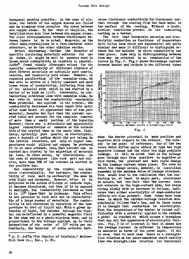
Vacuum Tube Design
hexagonal packing possible. In the case of alu-mina, two thirds of the oxygen spaces are filledand an aluminum atom occupies the space betweensix oxygen atoms. In the case of beryllia, theberyllium atom also lies between six oxygen atoms.The close correspondence between the distance be-tween layers is to be noted. Magnesia, on theother hand, crystallizes in a face -centered cubicstructure, as do the other alkaline earths.
Before discussing further the behavior ofspecific insulating materials suitable for use
in tubes, it might be well to examine what isknown about conductivity in crystals in general.Joffe6 found widely divergent values for thespecific conductivity of different crystals ofsuch diverse materials as optically pure quartz,calcite, and chemically pure alums. However, byrepeated purification of the ammonium alum, hewas able to arrive at a fairly constant and muchlower value of conductivity, differing from thatof the material with which he had started by afactor of as high as 1:100. Conversely, by con-taminating potassium alum with ammonium alum, hewas able to raise the conductivity enormously.When potential was applied to the crystal, theconductivity decreased ata very rapid rate untilafter some hours it approached that of the purematerial, despite the fact that the current car-ried could not account for the complete removalof more than a small portion of the impurity.However, there was a detectable and appreciablyhigher concentration of ammonia on the cathodeside of the crystal than on the anode side. Simi-larly, optically pure quartz, on electrolysis,gave a deposit of sodium which did not belong inthe lattice structure, and only at higher tem-peratures could silicon and oxygen be produced.It is at once evident, then, that current can becarried lea crystal by the migration of materialas ions, in other words, by electrolysis. Inthe case of substances like rock salt and cal-cite, more than 99% of the current is carried bythe positive ion.
But conductivity in the crystal can alsooccur electronically. For instance, the conduc-tivity of rock salt is ordinarily the same inboth light and darkness. However, after it is
subjected to the action of X-rays or cathode rays,it becomes discolored, and then if it is exposedto sunlight, its conductivity increases so thatit is 10 times that in darkness. This effectis not peculiar to rock salt but is characteris-tic of a large number of materials. The conduc-tivity is not decreased by reduction of the tem-perature to that of liquid air. With a given in-tensity of light, the current through the crys-tal can be deflected by a powerful magnetic fieldin the same way as a photo -electron beam, and isproportional to the voltage applied, up to fieldintensities of the order of 105 volts per cm.Similarly, the behavior of oxide cathodes indi-
6 A. F. Joffe,"The Physics of Crystals," McGraw-Hill Book Co., Inc., p. 81.
cates electronic conductivity for thermionic cur-rent through the coating from the base metal tothe surface of the coating. Without a doubt,similar conditions prevail in the insulatingcoating on a heater.
The fact that thermionic emission and elec-trolytic conduction as functions of temperatureboth follow laws which are exponential and quitesimilar has made it difficult to distinguish be-tween the two methods by which conductivity cantake place. Some help in distinguishing betweenthem may be obtained by an examination of thecurves in Fig. 2. Fig.2 shows the leakage currentbetween heater and cathode in two different tubes
TL
-152-20 - 5
POTENTIAL-O -5 0 +5 +0 +5 +20
BETWEEN HEATER A CATHODE (EHK)-VOLTS
Fig. 2
ks
when the heater potential is made positive andnegative with respect to the cathode. The cath-ode is the point of reference. One of the twotubes which differ quite widely in type has highnegative leakage and the other has high positiveleakage. It will be noted that as the voltagegoes through zero from positive to negative orvice versa, the greatest and moat rapid changein the leakage current takes place. The rate atwhich the change occurs, however, is controlledsomewhat by the maximum value of leakage attained.This would lead to the conclusion that the con-duction is, at least in major part, electronicin nature, but the fact that the current doesnot saturate on the high -current side, but keepsrising slowly with an increase in voltage, indi-cates that either electrolytic or semi -conductoreffects are also present. Some tubes have beenseen in which the current -voltage relation sub-stantially follows Ohm's law, and in these casesit is thought that conduction is electrolytic.
When the temperature of the heater is raised suf-ficiently with a potential applied to the cathode,a point is reached at which occurs a breakdownthat has all the appearance of electrolytic fail-ure. Fig. 3 is of interest in that it shows howthe leakage current is affected by temperatureas measured in terms of the power input. It will
be seen that in each case there is a straight-line relation on the power -emission chart exactlylike the straight-line relation for thermionic
28
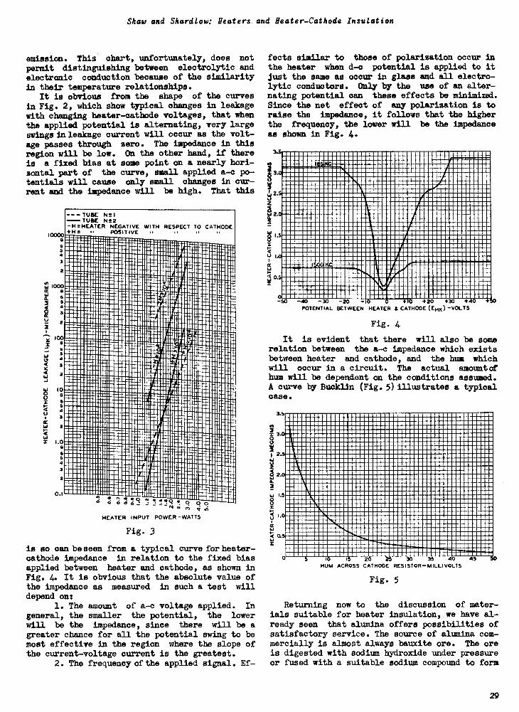
Shaw and Shardlow: Heaters and Heater -Cathode Insulation
emission. This chart, unfortunately, does notpermit distinguishing between electrolytic andelectronic conduction because of the similarityin their temperature relationships.
It is obvious from the shape of the curvesin Fig. 2, which show typical changes in leakagewith changing heater -cathode voltages, that whenthe applied potential is alternating, very largeswings in leakage current will occur as the volt-
age passes through zero. The impedance in thisregion will be low. On the other hand, if there
is a fixed bias at some point on a nearly hori-zontal part of the curve, small applied a -c po-tentials will cause only small changes in cur-rent and the impedance will be high. That this
100006
'' iiiiii iiiii inifibl=5
iiiiiiii .. iiiiiiiiiii- llll IA lllll aa
3 , lllllll 1111111:1911111MPRIAllinanni.111.11MMENIMILIMPNIIRE
HAFINIIIIPMEM0i, 1 Mar lll inishopigiumiwiiHaihpiammilidg. a. (x"--.1:11011:4113:HreihrmagivilinallieuhlLL
iI:- ........aidchimdelarandthisondi.....71 lllll I llllMilningtilgirititillIMEMBININ....5 l IMMO laity
2mr,11111 .......11=2241:
l 1 l
11:11INIMMOMMI lllllll..
inummensoupsnma; suni im hIllhalliill
au-,' 1CommupsumnormehdidilliMINO"..
id_ . 10.1M...1-;;".;=ogiluiliqpainiitepedilimill
W-T . 61:: lllllll Kirinanudar,iiiir NA "Iiiiiiingli-4O 691"""IIIIIIIIIIMIIIIIVAP ' ' 119111111<.v. sunismusyses jp, p iputl 11 ll Illinidini
1.rquiration .41min.., . lll inum=2-::::IP mourillahliNl-Mt-raw0
x MC lir..llllll 1: ' mpg LHs Holz on llllllSIN 11 1111U161111111111B BM I Uluu Lig! RAU rauninageldrinumW
s WI Ulan gnaw inpuusteutumerelosenw
La.. :irmrniikrilingtandkrearhiniq
ll iiiiinnihugarnl in nammuhann.= Lon: lllllnr:::-Eir. ,,A111: .:E.....sozp:66
l 3111.-.0inuntiiiiditinilididiuninnimminnunpoinimummermitem3 l 12311111111Omme. NM lllllSUM lllllll unineli.
RN IIin11111111.MM111111.21
lllll NIS lllll 11111111111111 NMISUMIUMMIIIIIIIMMINIFismy umiumiessussou.. faidadi llii: ll Iffilliiiindlittill0.1
- - - TUBE N2 I- TUBE N22-II =HEATER NEGATIVE WITH RESPECT TO CATHODE+PI= 44 POSITIVE
Om lllll1111111111111t11111111111 11 llllllll
" °f q q-N q
HEATER INPUT POWER -WAITS
Fig. 3
is so can be seen from a typical curve for heater -cathode impedance in relation to the fixed biasapplied between heater and cathode, as shown inFig. A. It is obvious that the absolute value ofthe impedance as measured in such a test willdepend on:
1. The amount of a -c voltage applied. Ingeneral, the smaller the potential, the lowerwill be the impedance, since there will be agreater chance for all the potential swing to bemost effective in the region where the slope ofthe current -voltage current is the greatest.
2. The frequency of the applied signal. Ef-
fects similar to those of polarization occur inthe heater when d -e potential is applied to itjust the same as occur in glass and all electro-lytic conductors. Only by the use of an alter-nating potential can these effects be minimized.Since the net effect of any polarization is toraise the impedance, it follows that the higherthe frequency, the lower will be the impedanceas shown in Fig. 4.
xc
T
-40 -30 -20 -10 0 10 +20 +30 +40 +POTENTIAL BETWEEN HEATER & CATHODE (EHK) -VOLTS
io
Fig. 4
It is evident that there will also be somerelation between the a -c impedance which existsbetween heater and cathode, and the hum whichwill occur in a circuit. The actual amount ofhum will be dependent on the conditions assumed.A curve by Bucklin (Fig. 5) illustrates a typicalcase.
3.5
03.0
2I 2.5
Zt
0 2.
2
rc
X
1.5
1.0
0.5I
0 5 10 15 20 25 30 35 40 45HUM ACROSS CATHODE RESISTOR -MILLIVOLTS
Fig. 5
Returning now to the discussion of mater-ials suitable for heater insulation, we have al-ready seen that alumina offers possibilities ofsatisfactory service. The source of alumina com-mercially is almost always bauxite ore. The oreis digested with sodium hydroxide under pressureor fused with a suitable sodium compound to form
10
29
Vacuum Tube Design
sodium aluminate which is soluble in water andcan be separated by filtration from impuritiessuch as iron and silicon which are rendered in-soluble by this treatment. By seeding the cooledfiltrate properly, it is possible to precipitatehydrated alumina and separate it by filtration.After washing, the product becomes the base ma-terial for the aluminum industry as well as forour insulation. Due to the fact that commercialaluminum is prepared from a bath of sodiumpinmi-num fluoride by electrolysis, not much attentionneed be paid to the sodium content. For our pur-pose, however, the alkali content is very im-portant, and it is necessary to make further ef-forts to remove it. This can be done by acidwashing of the alumina, which has been fired toa temperature of about 900°C to convert it par-tially to a alumina and render it insoluble. Inthis way, the alkali content, calculated as Na20,can be reduced to less than 0.2%. Another methodeffective in the removal of the alkali consistsin fusing the material in an electric -arc furnace,wholly converting it to a alumina, or corundum,and volatilizing much of the alkali by virtue ofthe high temperature attained. The fused mass,however, is very hard (9 on Mohts scale) and pre-sents great difficulty in grinding. For our work,grinding is done in an iron mill, and the groundmaterial is treated with acid to eliminate theiron introduced. The acid washing also serves toeliminate further any alkali left. Neither ofthe two processes does much towards a reductionin the silica content.
When the materials are received, the acid -
washed alumina is designated as "acid -washedbauxite -ore concentrates," and the acid washedfused material is known as "alundum." The baux-ite -ore concentrates require further treatmentin the factory before they are ready for use,while the alundum does not. The precipitatedalumina requires calcining at 1600°C to completethe conversion of the material to a alumina andthereby reduce the firing shrinkage, and subse-quent grinding to attain the desired particlesize. Milling is carried out in rubber -linedmills with either mullite or flint b"1 s forgrinding in order to keep to a minimum the im-purities introduced at this operation.
Alumina is mixed with a spraying binder con-taining nitrocellulose by WI -I -milling the mater-
ials together in a porcelain ball mill. The
alundum does not require ball -milling with thebinder, and can be mixed by rolling the two to-gether in a bottle. This difference in mixingprocedure is necessary because of the differencesin particle shape of alundum and alumina. Thealundum being a crushed, fused product has angu-lar faces on the particles while the calcined,precipitated material has particles approachingspheroids. These round grains aggregate readilyand need a milling or crushing action to sepa-rate them so that each grain will be wet by thebinder to give a smooth spraying mixture.
There are, in general, four methods of in-
sulating a heater from the cathode: (1) the useof an extruded sleeve between the heater wireand the cathode; (2) application of insulatingmaterial to the heater by dipping the heater wirein a suspension of the insulating mixture; (3)spraying a mixture similar to a dip mixture onthe heater; and (4) application of insulatingmaterial by electrodeposition or cataphoresis.
The extruded sleeve method is nearly obso-lete. The chief disadvantages of insulating aheater by this method were slow heating time andexcessively high operating temperatures of theheater wire.
The method of coating by dipping has severaldisadvantages when applied to helical heaters butmay be used to advantage for folded heaters. Inthe latter case, the wire is coated by the drag -coating process (which is a modification of theolder dipping process) before being formed intoheaters. The folded type of heater shows somecost advantages.
At the present time the great bulk of ourheaters are of the double-helical type using asprayed -insulation coating. The cost of manufac-turing such a heating element is high comparedwith other types but this type has electrical andmagnetic advantages.
The last method of applying coating to heaterwires is by cataphoresis. In this method, thesuspended particles of insulating material areapplied to the wire by making the heater an elec-trode in the suspension and using a sufficientpotential of the proper polarity to build up thedesired thickness of coating on the wire. Atthe present time this method is still in develop-ment, and little can be said about it except thatit holds some promise.
Regardless of the method of application, thetype of coating is dependent on: (1) the fine-ness of grain of the insulating material; (2)the shape of the grain; (3) freedom from aggre-gates of the material in the binder; (4) theviscosity of the coating mixture; and (5) thespeed of application.
Spray mixes should be made from material offine grain size (90% or more of the particlesshould be smaller than 4 microns and no parti-cles greater than 30 microns), free of aggregates,and of a viscosity sufficient to keep the parti-cles suspended. Rapid, wet spraying results ina smooth, dense coating which has a tendency tocrack during firing. Slow, dry spraying resultsin a fluffy, granular coating which is looselybonded to the wire and tends to chip when theheater is inserted in the cathode. The fine
grain is necessary to insure a compact, rela-tively smooth coating without spraying "wet",since the particles strike the wire at random,and fine grains give a more compact coating withgreater mechanical strength than do larger parti-cles.
Drag -coating mixtures can be made with ma-terial of larger grain size than that used forspray mixes and still yield a smoothly coated
30
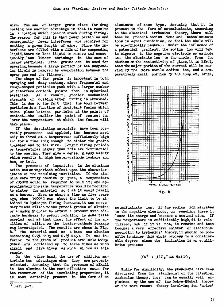
Shaw and Shardlow: Heaters and Heater -Cathode Insulation
wire. The use of larger grain sizes for dragcoating has another advantage in that it resultsin a coating which does not crack during firing.The reason for this is that fewer particles andconsequently fewer interfaces are required forcoating a given length of wire. Since the in-terfaces are filled with a film of the suspendingliquid, there is less liquid to remove and conse-quently less linear shrinkage in the case of
larger particles. Fine grains can be used forspraying, because a large portion of the suspend-ing liquid is removed by evaporation between thespray gun and the filament.
The shape of the grain is important in bothspraying and drag coating, since fragmental andrough -shaped particles pack with a larger numberof interface contact points than do sphericalparticles. As a result, greater mechanicalstrength of coating after firing is obtained.
This is due to the fact that the bond betweenparticles is a function of incipient fusion whichtakes place between particles at the points ofcontact-the smaller the point of contact thelower the temperature at which the fusion willtake place.
If the insulating materials have been cor-rectly processed and applied, the heaters needonly be fired at a temperature sufficiently highand for a time long enough to sinter the grainstogether and to the wire. Longer firing periodsor temperatures higher than this are detrimentalto the coating. They give a dense, glassy matrixwhich results in high heater -cathode leakage andhum, or both.
The presence of impurities in the aluminumoxide has an important effect upon the character-istics of the resulting insulation. If the alu-mina were truly chemically pure, a temperatureof 20500C would be required to melt it; and ap-proximately the same temperature would be requiredto sinter the material so that it would remainon a heater. Even as short a time as five yearsago, when 1600°C was about the limit to be at-tained in hydrogen firing furnaces, it was neces-sary to add silica to the purest grades of aluminaor alundum in order to obtain a product with ade-quate hardness to permit handling. In some testscarried out at that time, the effect of the ad-dition of silica on the heater -cathode leakagewas investigated. The results are shown in Fig.6.7 The material used as a base was alundumcontaining 0.7% Si02 and 0.3% Na20. It was in-ferior to the grade of product available today.
Other lots contained up to three times as muchalkali and five times as much silica as thissample.
On the other hand, the use of addition ma-terials has advantages when they are properlyselected. Assuming that the presence of alkaliin the alumina is the most effective cause forthe reduction of its insulating properties, itis most certainly present in the form of an
7 Ref. 3-7.
aluminate of some type. Assuming that it is
present in the form of metaaluminate, accordingto the classical Arrhenius theory, there willthen be present sodium ions and metaaluminateions in equal quantities, so that the whole willbe electrically neutral. Under the influence ofa potential gradient, the sodium ion will tendto migrate to the negative electrode or cathodeand the aluminate ion to the anode. From thestudies en the conductivity of glass, it is likelythat the major portion of the current will be car-ried by the more mobile sodium ion, and a com-paratively small portion by the complex, large,
166
8t.)
3T
g 6
4 5la
l*J 4
3
cow
2cccc
V
W 0-J
MMMMMMMMM MEMMEMOIMMESSEM MMMMM MEMO
MOMOMMEMEMMOMMMOMMMEMMOMMEMMOMMEMmmillMMOMMEMEM
MMMMM MMMMMMMMMMMM MIIMMEMOMMEMENOMMMMM IMMEMMINIMMOMMESEMOMMIMMEMEMMUMOMMMMMMMMMMMMMMMM MOOMMEMMOMMMOMMOMMOOMINIMMOOMMEIMMOMMOMMEMOMMEMMMOMMOMmmiliniMOOMMEMOMMMEMMUMMAIMMOMMOMUM
En MMMMMM SO MMMMM MEM MMMMM 111MMEMMOMOMMEMMORMMOMMOMME MMMMM MOMMOIMSMOMMOMMEMOMONSOMMWOOMMEMOMMEMOOMOEMOMMEMMEMOMMMEMMOMMEMSOMMOOMMOOMMEmOMMOMMEMOMIMEMOMOMMEMOMMEMMOMMINIEMMMMMM ONIMMEMMOMMEMMOMOMMEMOMMEMOMMOMMIIMMUMOMMIMMOMMEMMOMMUSOMMMEMOMMEMROMMEMMEMMIIRMSOMMEMEMMallMMMMM NOMEMSMOOMOMMEMOMMOMMOMMOOMMEMOMMEMOMMEMOMMEMOMMEMSMOMOMMEMOMMUMNSEMEMMOMOMMMUMMOMMESMOOMMOMMINIMMEMMOMMEMIOmumminsommommummmilimmusimmonsMMMMMM MMMMMM MOMMEMSOMMUMMEMME
EMOMMEMEMOMMEWOMMEMMOMMEMEMOMMEMMIMMEMOMMOSOMEMMOMMSOMOOMUMMOMMENOMMOMMEMOMMEMOMMEMMOMMIONOMMOOMMEMMOMMEMmEMOMMMMUMSOMMOSINSMOOMMMEMCMUMMOMMEMMOMMEMUMMOSOMMEMOMMEMOMMEMOSIIMMEMOMMMEMMEMEMEMOMMOMMOMMUISSMEMEMMIIIMMMOMMOSEMMMEMEMOOMMOMMOMMOMUMMMOIMMINIMMOOMMEMOMMOINIMMONMEMMOOMMEMMOMOMMMOMOMMOMMEMOMMOMMOrMEMITIMMOMMEMMEMMOMMMOMMOMOMSOMINEMOmmMUMMimmon MMMMMMMMMMMMMMM BMW" OEM
MMMMM MOMMErmiliMMOMMMOmoMMOXIMMOMMOMOMOOEMMOMMINUMUMMOMEMUMIMMOMMOMMOOMMOMMMMMUNIUMEMOMUMMO
MIIMEMMUSMOMMEMEMOMEMIUMMEMOMMEMMINgOM MMMMM MMMMM 11111MIMAMOOMMMOMMEMEm
IrliniMMEMEn MMMMMMM r MM MMINIMMEMMEMME
...Ammilmommumm MMMMMMimm _ ---.;. mem. MMMMMMMMMMMM eimffiemmommunnommolll111
2 3 4 5 6
TOTAL SILICA -PER CENT
Fig. 6
metaaluminate ion. If the sodium ion migratesto the negative electrode, on reaching there itloses its charge and becomes a neutral atom. If
the temperature is sufficiently high, it is vola-tilized, but if it is not, it remains and thenbecomes a very effective emitter of electrons.According to Arrhenius' theory, it should be pos-sible to hinder this whole process to a consider-able degree since the ionization is an equili-brium process:
Na+ + A102 NaA102
While for simplicity, the phenomena have beendiscussed from the standpoint of the classicalArrhenius theory, they can be equally well ex-
plained by the use of the Debye-Rickel theoryor the more recent theory involving ion wholes"
31
Vacuum Tube Design
as discussed by Schottky8 and deBoer.9 By in-creasing the concentration of the aluminate ion,the reaction can be driven to the right, thus re-ducing the concentration of the sodium ions sincethe product of the two concentrations is a con-stant for any temperature. This can be accom-plished by adding metaaluminates in which thepositive ion is one which does not migrate withthe facility of the sodium ion, e.g., the alka-line earth metals. A series of experiments inwhich tests were made on insulation of aluminaand of the same alumina with the addition of 1%of the various alkaline -earth oxides very wellillustrates this behavior as shown in Figs. land8. Here the impedance between heater and cath-
76
4
te)2
1
0
2
00
I
2
6WI- 6
W S
4
3
2
0.1 -300 -200 -I
174Ba0
i
170m90
19. Sr0.
1001.A 203
:1 1.. coo ',Aro-la Ll
I00 9A 203
CaOI
I
TYPEE f .6.3
77VOLTS
APPLIED SIGNAL 7,
(E.c)=0.5 V -SIGNAL FREQUENCY=
100000 CPS'
POTENTIAL BETWEEN HEATER & CATHODE (EHK )-VOLTS
Fig. 7
ode at various values of fixed bias was measuredwhen a signal of 0.5 volt was impressed at a fre-quency of 100000 c.p.s. It was found that theaddition of each of these materials was effec-tive in reducing the conductivity of the un-treated alumina to various degrees. A largeamount of practical experience indicates that abarium -oxide addition is the most effective ofthose things tried. The strontium oxide used forthe test was of commercial grade, and it would beexpected that a purer grade would lead to super -
8 Schottky, Naturwissenschaften, 23, 656; 1935.Z. physik. Chem. (b) 29, 335; 1935.
9 DeBoer, Recueil Des Travaux Climiques Des.Pays -Bas, 56, 301-390; March, 1937.
for results. It was found from a study of thecurves that whereas the tops are flat in the caseof alumina even at high temperature and highbias, in each of the other cases there is a ten-dency for the insulation to decrease under theseconditions. This can be explained by the factthat at high temperatures the larger barium ionshave a greater mobility and can move under theinfluence of the higher potentials. That this isso is borne out by the fact that intermittentlife tests at 8.5 volts on 6.3 -volt heaterswith 180 volts bias between heater and cathodeshow more failures in the cases where additionshave been made than in the case of alumina alone.In the case of 6.3 -volt life tests, there ap-
100
19 Ba 0r7
I BaO
11.10 1I
I 'Phis° -- NCaI 0,- 100 /0A1203
SU : - 7.,-- 1I -
ti 1t,
I 7C a 0,..1:0:A1203u
1,4r0I=TYPE 77E f .7.9 VOLTS -APPLIED SIGNAL -
(Eac)= 0.5 V _li SIGNAL FREQUENCY=
-100000 CPS
2
1
4
3
2
65
4
3
2
0.1 -300 -200 -100 0 +100 +2POTENTIAL BETWEEN HEATER & CATHODE (EHK) -VOLTS
Fig. 8
pears tto be no similar difference. Work byBenjaminle has indicated that beryllia additionsare even more effective than baria, but experi-ments in this laboratory have not been conclu-sive on this point.
From some studies of the use of electrolyticas compared with metallurgical tubing, there isavailable very good evidence of how the condi-tions of use affect the insulation between heaterand cathode. For reasons connected with tubecharacteristics, it was found to be more desir-able to use electrolytic tubing for the cath-ode sleeve than to use the metallurgical nickelstandard at that time. It was found that theoperating temperature was substantially higher
10 Private communication to author.
32

Shaw and Shardlow: Heaters and Heater -Cathode Insulation
with the electrolytic tubing and a constant in-put wattage, and consequently it was necessaryfor the heating element to function at a cor-
respondingly higher temperature to attain the
3
HEATER VOLTS (Ef)
Fig. 9
necessary heat transfer and the proper emission.This is illustrated in Fig. 9.11 From this, itcan be seen that there is a difference of about500K between the two cathodes and this has the
11 Ref. 3-11.
pronounced effect on the heater -cathode leakageas shown in Fig. 10. It will be seen that at theoperating point, the temperature difference ac-counts for a change in the leakage by a factorof about 5:1. At the same time, the differencein temperature of the heaters as operated is
9
I.
5
4
3
2
0
S
3
.6
.5
.2
0I
-AM1=11111111111MIMININNWMINIII=.1.==.111MINNIMENEMMII
11111111111/111mrAIM:171.:12=
MIN ell/AM=1
MOM MN v MM. se.AIMIIIM
,.'411111 AAIIIIIIII;4111111
WIRTMTOAMMIIMMEMOMMIENII
214Annummumni11111111111111111111111
111111111111111I8 2 2 2 6
HEATER NADOS ( E
Fig. 10
shown by a small but consistent difference inthe heater current, indicating a higher resist-ance and a correspondingly higher temperaturefor the one enclosed by electrolytic nickel.
30
33
Lecture 4
PHOTOELECTRIC AND SECONDARY EMISSION
L. B. Headrick
Part I - Photoelectric Emission
INTRODUCTION
The discussion will be limited to the externalphotoelectric effect or the emission of elec-trons from the surface of a conductor or semi-conductor upon the absorption of visible andnear -visible light by the first few hundred atomiclayers near the surface. Characteristics ofclean metals, thin films of one metal on anothermetal, metals with a thin oxide layer on the sur-face, and composite surface layers of a metal -metal oxide semiconductor will be considered.Photoconductivity in crystals and the barrier -layer photoelectric phenomena, such as seleniumand copper -oxide cells, will not be considered,except with respect to one item, namely, the ef-ficiency of light-sensitive devices.
Einstein in 1905 made the first theoreticaladvance in an attempt toward an explanation ofphotoelectric phenomena when he postulated thatlight must be adsorbed, as well as emitted, inquanta of energy by , and if one quantum is ad-sorbed by one electron, the following relationmust hold:
where
h
hU - Lo = 1/2 mv! = el/ma.
hO = Eomax
frequency of incident light= 1/wavelength X= Planck's constant
so = minimum energy required to re-move an electron from the met-al to free space or vacuum
m = electron massvmax = velocity of the fastest
emitted electronsVmax = the retarding potential re-
quired to stop the fastestelectrons
The frequency of light which will just ejectelectrons with zero velocity is called thethreshold frequency (v0) and is defined by
hVo = 5o
The corresponding threshold wavelength orwavelength limit ( X0) may be defined by
h/Xo = Eo
After Einstein, the next important theoreticaladvance in the field of photoelectric emissionwas made by Sommerfeld in 1928 with the introduc-tion of the electron theory of metals. Thistheory failed to explain all of the observedphotoelectric phenomena because the electronsand atoms were assumed to be in thermal equilib-rium. Later Sommerfeld applied the Fermi-Diracstatistics to electrons in metals where the elec-tron energy distribution extends over a rangefrom zero to a definite maximum value at 00K.Since photoelectric emission involves the inter-action between a quantum of light and the elec-trons near the surface of a metal, it is essen-tial to have a satisfactory theory of electronsin metals in order to have a sound basis for atheory of photoelectric emission. The Fermi-Dirac statistics applied to the electron theoryof metals has been used quite successfully to ex-plain a number of the observed characteristics ofphotoelectric emission with no important dis-crepancies and,therefore, appears to satisfy theabove requirement.
A. PHOTOPTRCTRIC EMISSION FROM CLEAN METALS ANDTHIN METAL FILMS
1. Energy Distribution of Photoelectrons
The total energy distribution characteristicof photoelectrons for different temperatures isshown in the upper part of Fig. 1 by the solidand dashed curves, as calculated from the Fermi-Dirac theory. These curves show that only at atemperature of 00K is there a definite, sharplimiting value of electron energy in a metal andthat at higher temperatures there are increasingnumbers of electrons with higher energies as thetemperature increases. Therefore, the theoryindicates that the energy distribution of elec-trons emitted by monochromatic light of a givenwavelength will only have a sharp limit at 0°Kand will tail off at higher temperatures. Thetheory agrees with observations. However, untilvery recently, experimental observations did notfit the calculated curves closely at the lowervalues of energy. The departure of the older ex-perimental details shown by the dotted curve. Us-ing thin films of potassium, C. L. Henshawl has
long 1 C. L. Henshaw, "Normal Energy Distribution ofPhotoelectrons from Thin Potassium Films as aFunction of Temperature," Physical Review, Vol.52, No.8, p. 854; October 15, 1937.
34
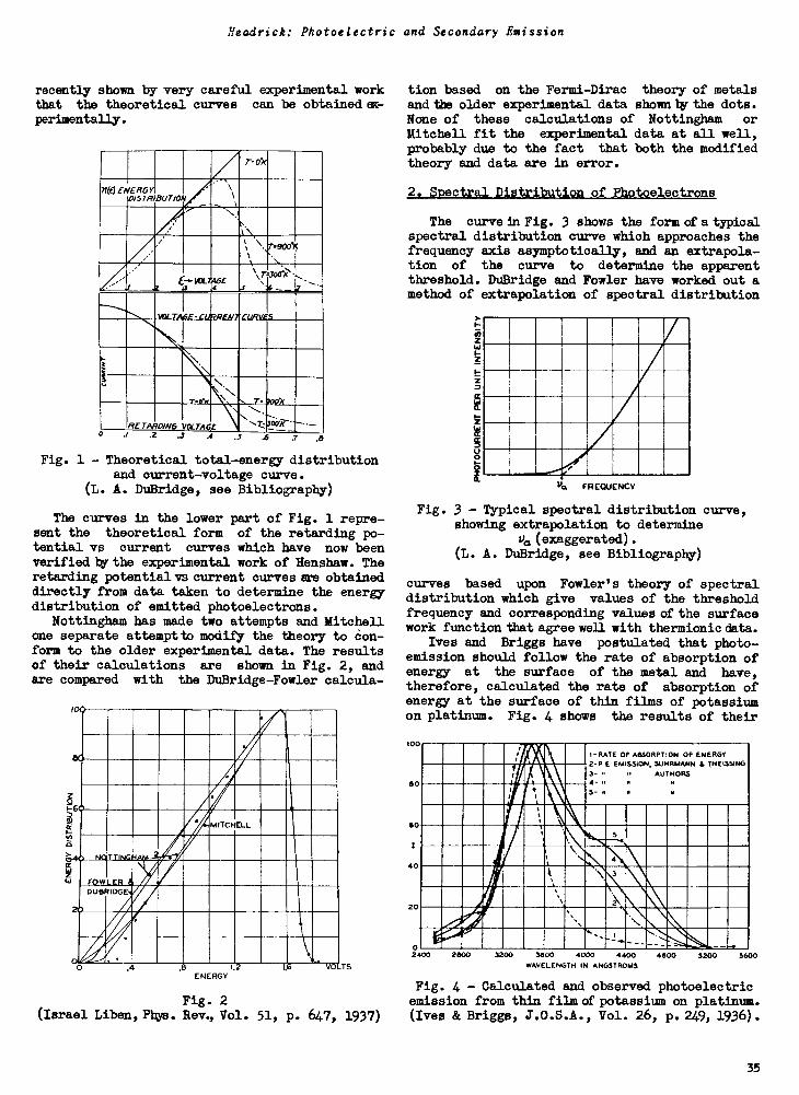
Headrick: Photoelectric and Secondary Emission
recently shown by very careful experimental workthat the theoretical curves can be obtained ex-perimentally.
7. 0.1(
710 ENERGYIDISTRIBUTION
'
-\
--..... 1.
,T.\
1 t \% . .900K
..I .26-1. VOLa
AGE.4
\rzisoo)i-,,2 lc - -7 -
VOLTAGE,CLNRENT CLIRV05
v.x .N.\I
rre4
N.,N.
N.. T. 9001E
RETARDING 101..TAGE
\ .
`,..-T 007( ----- - .s .6 .7 .6
Fig. 1 - Theoretical total -energy distributionand current -voltage curve.
(L. A. DuBridge, see Bibliography)
The curves in the lower part of Fig. 1 repre-sent the theoretical form of the retarding po-tential vs current curves which have now beenverified by the experimental work of Henshaw. Theretarding potential vs current curves are obtaineddirectly from data taken to determine the energydistribution of emitted photoelectrons.
Nottingham has made two attempts and Mitchellone separate attempt to modify the theory to con-form to the older experimental data. The resultsof their calculations are shown in Fig. 2, andare compared with the DuBridge-Fowler calcula-
cc
0
CCCC
Li
Li
fvt,
AO
0I
let NQTTINGiA
,..../M1TC'HELL
FOWLERI
a/r
DOSIRIDGE
20
\.....Dn
01-'
a A 13 16 VOtENERGY
TS
Fig. 2(Israel Liben,Phys. Rev., Vol. 51, p. 647, 1937)
tion based on the Fermi-Dirac theory of metalsand the older experimental data shown by the dots.None of these calculations of Nottingham or
Mitchell fit the experimental data at all well,probably due to the fact that both the modifiedtheory and data are in error.
2. Spectral Distribution of Photoelectrons
The curve in Fig. 3 shows the form of a typicalspectral distribution curve which approaches thefrequency axis asymptotically, and an extrapola-tion of the curve to determine the apparentthreshold. DuBridge and Fowler have worked out amethod of extrapolation of spectral distribution
vc, FREQUENCY
Fig. 3 - Typical spectral distribution curve,showing extrapolation to determine
Va(exaggerated).(L. A. DuBridge, see Bibliography)
curves based upon Fowlerls theory of spectraldistribution which give values of the thresholdfrequency and corresponding values of the surfacework function that agree well with thermionic data.
Ives and Briggs have postulated that photo -emission should follow the rate of absorption ofenergy at the surface of the metal and have,therefore, calculated the rate of absorption ofenergy at the surface of thin films of potassiumon platinum. Fig. 4 shows the results of their
10
60
60
40
20
O
t1 .I -RATE OF ABSORPTION OF ENERGY2 P E EMISSION; SUHRMANN I THEISSING3- 1* II AUTHORS4- u I.
5- I. II u
I ti
1
III,
t
'tt, \ 5
.\\I
tt
\Ns..., 4
t ..
.
11 \ 3\t
sst.
../541111111" s...... I- _ .....
2400 2600 3200 3600 4000 4400WAVELENGTH IN ANGSTROMS
4800 5200 5600
Fig. 4 - Calculated and observed photoelectricemission from thin film of potassium on platinum.(Ives & Briggs, J.O.S.A., Vol. 26, p. 249, 1936).
35
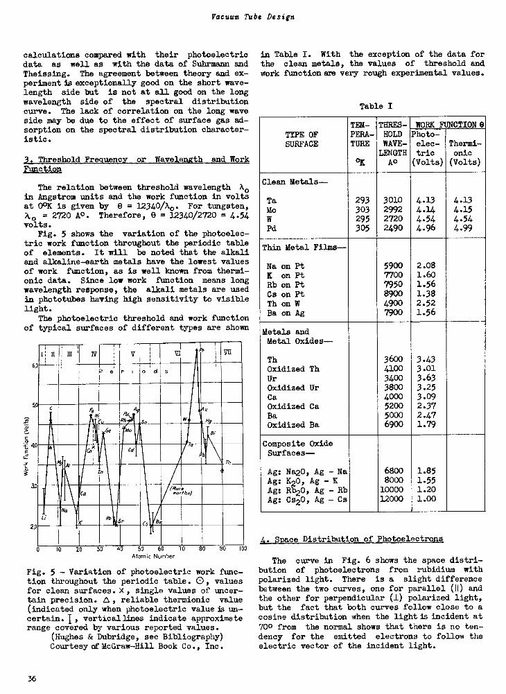
Vacuum Tube Design
calculations compared with their photoelectricdata as well as with the data of Suhrmann andTheissing. The agreement between theory and ex-periment is exceptionally good on the short wave-length side but is not at all good on the longwavelength side of the spectral distributioncurve. The lack of correlation on the long waveside may be due to the effect of surface gas ad-sorption on the spectral distribution character-istic.
3. Threshold Frequency or Wavelength and WorkFunction
The relation between threshold wavelength X0in Angstrom units and the work function in voltsat 00K is given by 0 = 12340/A0. For tungsten,A0 = 2720 Ao. Therefore, 0 = 12340/2720 = 4.54volts.
Fig. 5 shows the variation of the photoelec-tric work function throughout the periodic tableof elements. It will be noted that the alkaliand alkaline -earth metals have the lowest valuesof work function, as is well known from thermi-onic data. Since low work function means longwavelength response, the alkali metals are usedin phototubes having high sensitivity to visiblelight.
The photoelectric threshold and work functionof typical surfaces of different types are shown
1 i n1
IQ Dii
1
, Pert o d s
5A C
A. Au
N ,i/
Cu R SnW
H9
6e Mo
Ta
81
allCal
Ph
Th
o (RareCa ear MA)
Li Rb$r Ba
0Cs
5
4
2
0 0
Atomic Number
Fig. 5 - Variation of photoelectric work func-tion throughout the periodic table. 0, valuesfor clean surfaces. X, single values of uncer-tain precision. reliable thermionic value(indicated only when photoelectric value is un-certain. I, verticallinPs indicate approximaterange covered by various reported values.
(Hughes & Dubridge, see Bibliography)Courtesy of McGraw-Hill Book Co., Inc.
in Table I. With the exception of the data forthe clean metals, the values of threshold andwork function are very rough experimental values.
Table I
TYPE OFSURFACE
TEM-PERA-TUBE
°K
THRES-HOLDWAVE-LENGTH
Ao
WORK FUNCTION 6Photo -
elec-tric
(Volts)
Thermi-onic(Volts)
Clean Metals-
Ta 293 3010 4.13 4.13Mo 303 2992 4.14 4.15
W 295 2720 4.54 4.54Pd 305 2490 4.96 4.99
Thin Metal Films-
Na on Pt 5900 2.08
K on Pt 7700 1.60Rb on Pt 7950 1.56
Cs on Pt 8900 1.38Th on W 4900 2.52Ba on Ag 7900 1.56
Metals andMetal Oxides-
Th 3600 3.43Oxidized Th 4100 3.01
Ur 3400 3.63
Oxidized Ur 3800 3.25
Ca 4000 3.09Oxidized Ca 5200 2.37Ba 5000 2.47Oxidized Ba 6900 1.79
Composite OxideSurfaces-
Ag: Na20, Ag - Na 6800 1.85
Ag: K20, Ag - K 8000 1.55
Ag: Rt20, Ag -Rb 10000 1.20Ag: Cs20, Ag - Cs 12000 1.00
4. Space Distribution of Photoelectrons
The curve in Fig. 6 shows the space distri-bution of photoelectrons from rubidium withpolarized light. There is a slight differencebetween the two curves, one for parallel (Ii) andthe other for perpendicular (I) polarized light,but the fact that both curves follow close to acosine distribution when the light is incident at
700 from the normal shows that there is no ten-dency for the emitted electrons to follow theelectric vector of the incident light.
36
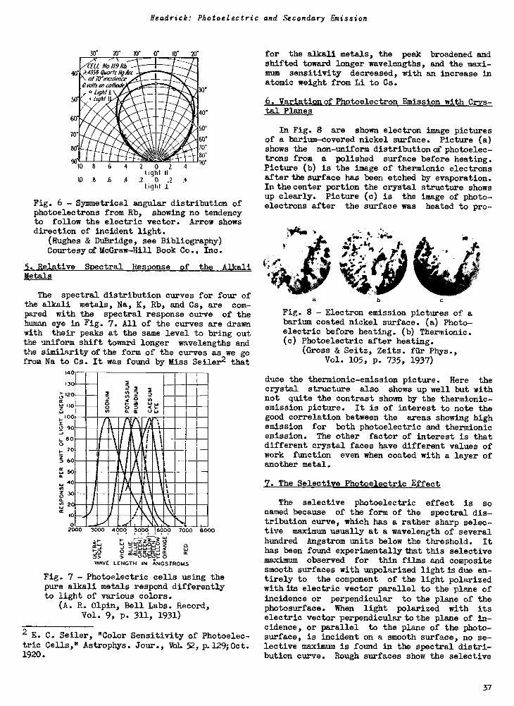
Headrick: Photoelectric and Secondary Emission
30- 20* 10'
/4LA0119a
011011 A#4.!**&
kr, A4358 alartz Ng kr'\ (rixidence
441111111atOres on ea/lrork
light ,
**KU -1Wift4A
so -
70'
9010
10 .8
2 0 2Ight II
.6 4 .2 0 .2light
A
so.
60°
70°
80*
90°
Fig. 6 - Symmetrical angular distribution ofphotoelectrons from Rb, showing no tendencyto follow the electric vector. Arrow showsdirection of incident light.
(Hughes & DuBridge, see Bibliography)Courtesy of McGraw-Hill Book Co.. Inc.
5. Relative Spectral Response of the AlkaliMetals
The spectral distribution curves for four ofthe alkali metals, Na, K, Rb, and Cs, are com-pared with the spectral response curve of thehuman eye in Fig. 7. All of the curves are drawnwith their peaks at the same level to bring outthe uniform shift toward longer wavelengths andthe similarity of the form of the curves as we gofrom Na to Cs. It was found by Miss Seiler2 that
140
130
120a
110
100
O 90
600
702 60cc 50a
N
02a10
02000 3000 4000 5000 16000
Crt,1-
D>
DpeeN3iO ..3-icaa ..1 a> 0
III 'fi 3
IV II-
IIMIIIHrilm.t"
WO II/110/nrill11111MIIIIIIM1111 M
111111111111111101/1111111 II
Ell IISKlint IliIMMUMIKI IliME HAMM M/I IAKIMMIIIMERENNEll
7000
a
WAVE LENGTH IN ANGSTROMS
8000
Fig. 7 - Photoelectric cells using thepure alkali metals respond differentlyto light of various colors.
(A. R. Olpin, Bell Labs. Record,Vol. 9, P. 311, 1931)
2 E. C. Seiler, "Color Sensitivity of Photoelec-tric Cells," Astrophys. Jour., VOL 52, p.129; Oct.1920.
for the alkali metals, the peak broadened andshifted toward longer wavelengths, and the maxi-mum sensitivity decreased, with an increase inatomic weight from Li to Cs.
6. Variation of Photoelectron Emission with Crys-tal Planes
In Fig. 8 are shown electron image picturesof a barium -covered nickel surface. Picture (a)shows the non -uniform distribution of photoelec-trons from a polished surface before heating.Picture (b) is the image of thermionic electronsafter the surface has been etched by evaporation.In the center portion the crystal structure showsup clearly. Picture (c) is the image of photo-electrons after the surface was heated to pro -
a
Fig. 8 - Electron emission pictures of abarium coated nickel surface. (a) Photo-electric before heating. (b) Thermionic.(c) Photoelectric after heating.
(Gross & Seitz, Zeits. ftir Phys.,Vol. 105, p. 735, 1937)
duce the thermionic-emission picture. Here thecrystal structure also shows up well but withnot quite the contrast shown by the thermionic-emission picture. It is of interest to note thegood correlation between the areas showing highemission for both photoelectric and thermionicemission. The other factor of interest is thatdifferent crystal faces have different values ofwork function even when coated with a layer ofanother metal.
7. The Selective Photoelectric Effect
The selective photoelectric effect is sonamed because of the form of the spectral dis-tribution curve, which has a rather sharp selec-tive maximum usually at a wavelength of severalhundred Angstrom units below the threshold. Ithas been found experimentally that this selectivemaximum observed for thin films and compositesmooth surfaces with unpolarized light is due en-tirely to the component of the light polarizedwith its electric vector parallel to the plane ofincidence or perpendicular to the plane of thephotosurface. When light polarized with itselectric vector perpendicular to the plane of in-cidence, or parallel to the plane of the photo -surface, is incident on a smooth surface, no se-lective maximum is found in the spectral distri-bution curve. Rough surfaces show the selective
37
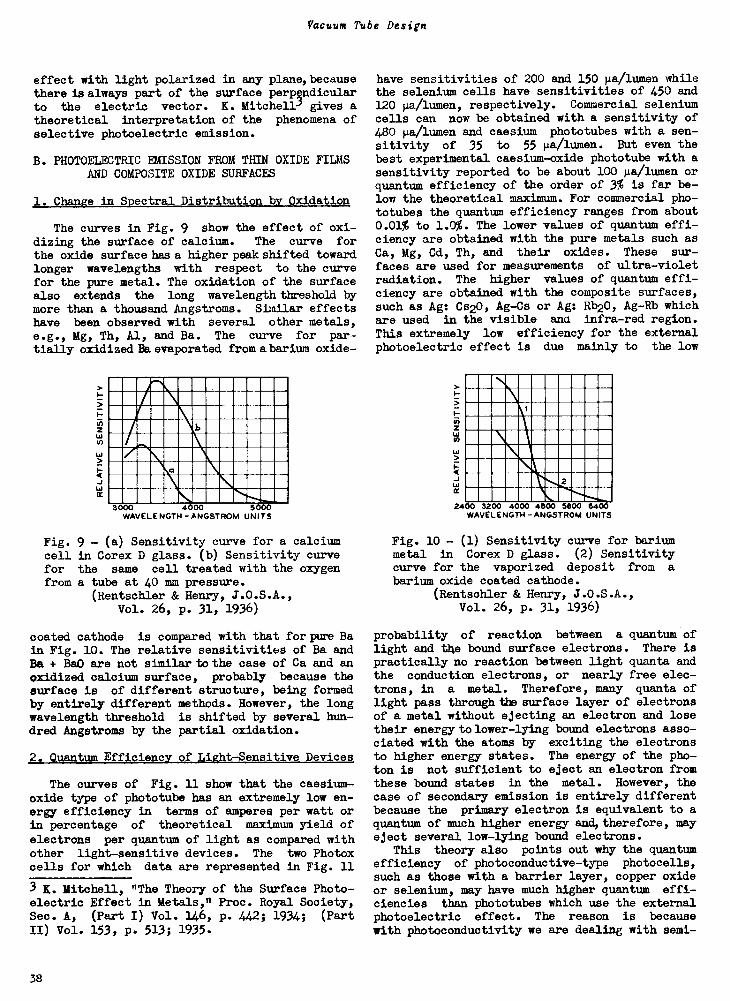
Vacuum Tube Design
effect with light polarized in any plane, becausethere is always part of the surface perpQndicularto the electric vector. K. Mitchell, gives atheoretical interpretation of the phenomena ofselective photoelectric emission.
B. PHOTOELECTRIC EMISSION FROM THIN OXIDE FILMSAND COMPOSITE OXIDE SURFACES
1. Change in Spectral Distribution by Oxidation
The curves in Fig. 9 show the effect of oxi-dizing the surface of calcium. The curve forthe oxide surface has a higher peak shifted towardlonger wavelengths with respect to the curvefor the pure metal. The oxidation of the surfacealso extends the long wavelength threshold by
more than a thousand Angstroms. Similar effectshave been observed with several other metals,e.g., Mg, Th, Al, and Ba. The curve for par-tially oxidized Ba evaporated from a barium oxide -
a
3000 4000 5000WAVELENGTH -ANGSTROM UNITS
Fig. 9 - (a) Sensitivity curve for a calciumcell in Corex D glass. (b) Sensitivity curvefor the same cell treated with the oxygenfrom a tube at 40 mm pressure.
(Rentschler & Henry, J.O.S.A.,Vol. 26, p. 31, 1936)
coated cathode is compared with that for pure Bain Fig. 10. The relative sensitivities of Ba andBa + BaO are not similar to the case of Ca and anoxidized calcium surface, probably because thesurface is of different structure, being formedby entirely different methods. However, the longwavelength threshold is shifted by several hun-dred Angstroms by the partial oxidation.
2. Quantum Efficiency of Light -Sensitive Devices
The curves of Fig. 11 show that the caesium -oxide type of phototube has an extremely low en-ergy efficiency in terms of amperes per watt orin percentage of theoretical maximum yield of
electrons per quantum of light as compared withother light-sensitive devices. The two Photoxcells for which data are represented in Fig. 11
3 K. Mitchell, "The Theory of the Surface Photo-electric Effect in Metals," Proc. Royal Society,Sec. A, (Part I) Vol. 146, P. 442; 1934; (PartII) Vol. 153, p. 513; 1935.
have sensitivities of 200 and 150 µa/lumen whilethe selenium cells have sensitivities of 450 and120 µa/lumen, respectively. Commercial seleniumcells can now be obtained with a sensitivity of480 µa/lumen and caesium phototubes with a sen-sitivity of 35 to 55 µa/lumen. But even thebest experimental caesium -oxide phototube with asensitivity reported to be about 100 µa/lumen orquantum efficiency of the order of 3% is far be-low the theoretical maximum. For commercial pho-totubes the quantum efficiency ranges from about0.01% to 1.0%. The lower values of quantum effi-ciency are obtained with the pure metals such asCa, Mg, Cd, Th, and their oxides. These sur-
faces are used for measurements of ultra -violet
radiation. The higher values of quantum effi-ciency are obtained with the composite surfaces,such as Ag: Cs20, Ag-Cs or Ag: Rb20, Ag-Rb whichare used in the visible and infra -red region.
This extremely low efficiency for the externalphotoelectric effect is due mainly to the low
2
2400 3200 4000 4800 5600 6400WAVELENGTH - ANGSTROM UNITS
Fig. 10 - (1) Sensitivity curve for bariummetal in Corex D glass. (2) Sensitivitycurve for the vaporized deposit from a
barium oxide coated cathode.(Rentschler & Henry, J.O.S.A.,
Vol. 26, p. 31, 1936)
probability of reaction between a quantum oflight and the bound surface electrons. There ispractically no reaction between light quanta andthe conduction electrons, or nearly free elec-trons, in a metal. Therefore, many quanta oflight pass through the surface layer of electronsof a metal without ejecting an electron and losetheir energy to lower -lying bound electrons asso-ciated with the atoms by exciting the electronsto higher energy states. The energy of the pho-ton is not sufficient to eject an electron fromthese bound states in the metal. However, thecase of secondary emission is entirely differentbecause the primary electron is equivalent to aquantum of much higher energy and, therefore, mayeject several low-lying bound electrons.
This theory also points out why the quantumefficiency of photoconductive -type photocells,such as those with a barrier layer, copper oxideor selenium, may have much higher quantum effi-ciencies than phototubes which use the externalphotoelectric effect. The reason is becausewith photoconductivity we are dealing with semi -
38
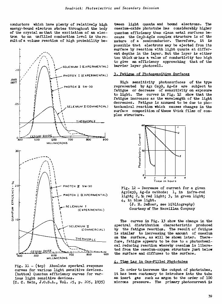
Headrick: Photoelectric and Secondary Emission
conductors which have plenty of relatively highenergy -bound electron states throughout the bodyof the crystal so that the excitation of an elec-tron to an unfilled conduction level is there-sult of a volume reaction of high probability be -
4 0
AMRvo577
.05
0400 500
30
, 20
z
117
2
<
aD
o
SELENIUM I (EXPERIMENTAL)
PHOTOX I (EXPERIMENTAL)
PHOTOX 3I SW -30
SELENIUM II (COMMERCIAL)
THERMOPILE
600 700MILLIMICRONS
PHOTOX II Sw-30
L. --I--i PHOTOX I (EXPERIMENTAL)
11 I
I I1 SELENIUM I
1
I
1 --(EXPERIMENTAL),
IUM OXICESDE0400 500 600 700
MILLIMICRONS
SELENIUM I((COMMERCIAL)
THERMOPILE
800 900
Fig. 11 - (top) Absolute spectral responsecurves for various light sensitive devices.(bottom) Quantum efficiency curves for var-ious light sensitive devices.(C. C. Hein, J.O.S.A., Vol. 25, p. 205, 1935)
tween light quanta and bound electrons. The
caesium -oxide phototube has considerably higher
quantum efficiency than clean metal surfaces be-cause the Cs20-AgCs complex structure is of thenature of a semiconductor. Therefore, it is
possible that electrons may be ejected from itssurface by reaction with light quanta at differ-ent depths in the layer. But the layer is eithertoo thick or has a value of conductivity too highto give an efficiency approaching that of thebarrier layer photocell.
3. Fatigue of Photosensitive Surfaces
High sensitivity photosurfaces of the typerepresented by Ag: Cs20, Ag-Cs are subject tofatigue or decrease of sensitivity on exposureto light. The curves in Fig. 12 show that thefatigue increases as the wavelength of the lightdecreases. Fatigue is assumed to be due to pho-tochemical reaction which causes changes in thesurface composition of these thick films of com-plex structure.
100
U
50U
0
04-
ti
00 2 3
Time in hours
2
3
4
4
Fig. 12 - Decrease of current for a givenAg:Cs20, Ag-Cs cathode: 1, in infra -red
light; 2,in red light; 3, in green light;4, in blue light.
(J. H. DeBoer, see Bibliography)Courtesy of The Macmillan Company
The curves in Fig. 13 show the change in thespectral distribution characteristic producedby the fatigue reaction. The result of fatigueis similar to increasing the amount of caesiumon the surface, as will be shown later. There-fore, fatigue appears to be due to a photochemi-cal reducing reaction whereby caesium is libera-ted from the caesium -oxygen structure just belowthe surface and diffuses to the surface.
4. Time Lag in Gas -Filled Phototubes
In order to increase the output of phototubes,it has been customary to introduce into the tubean inert gas such as argon to the order of 100microns pressure. The primary photocurrent is
39
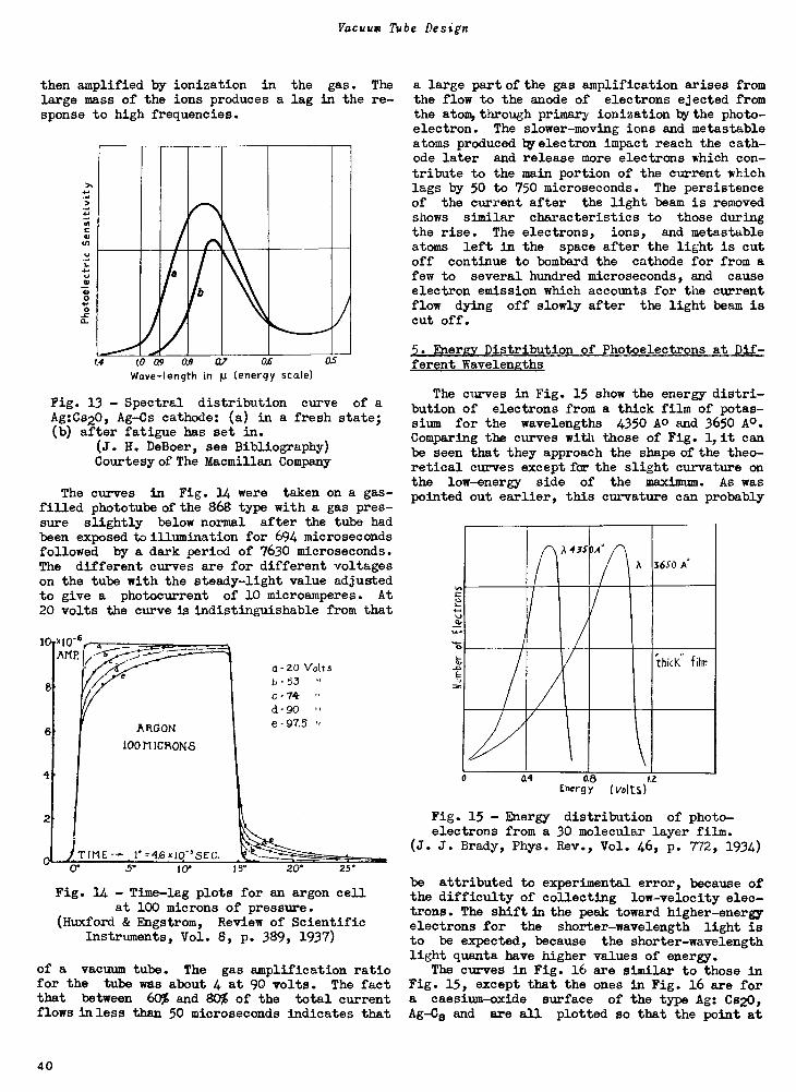
Vacuum Tube Design
then amplified by ionization in the gas. Thelarge mass of the ions produces a lag in the re-sponse to high frequencies.
a
4 IR 09 0.8 0.7 04
Wave -length in µ (energy scale)OS
Fig. 13 - Spectral distribution curve of aAg:Cs20, Ag-Cs cathode: (a) in a fresh state;(b) after fatigue has set in.
(J. H. DeBoer, see Bibliography)Courtesy of The Macmillan Company
The curves in Fig. 14 were taken on a gas -filled phototube of the 868 type with a gas pres-sure slightly below normal after the tube hadbeen exposed to illumination for 694 microsecondsfollowed by a dark period of 7630 microseconds.The different curves are for different voltageson the tube with the steady -light value adjustedto give a photocurrent of 10 microamperes. At20 volts the curve is indistinguishable from that
8
6
4
2
ARGON
100/11CR0NS
TIME rz4.6x10-'SEC.
U7
a-20 Volts
b-53c-74d-90e-ga.5
15* 20° 25.
Fig. 14 - Time-lag plots for an argon cellat 100 microns of pressure.
(Huxford & Engstrom, Review of ScientificInstruments, Vol. 8, p. 389, 1937)
of a vacuum tube. The gas amplification ratiofor the tube was about 4 at 90 volts. The factthat between 60% and 80% of the total currentflows in less than 50 microseconds indicates that
a large part of the gas amplification arises fromthe flow to the anode of electrons ejected fromthe atom, through primary ionization by the photo-electron. The slower -moving ions and metastableatoms produced by electron impact reach the cath-ode later and release more electrons which con-tribute to the main portion of the current whichlags by 50 to 750 microseconds. The persistenceof the current after the light beam is removedshows similar characteristics to those duringthe rise. The electrons, ions, and metastableatoms left in the space after the light is cutoff continue to bombard the cathode for from afew to several hundred microseconds, and causeelectron emission which accounts for the currentflow dying off slowly after the light beam iscut off.
5. Energy Distribution of Photoelectrons at Dif-ferent Wavelengths
The curves in Fig. 15 show the energy distri-bution of electrons from a thick film of potas-sium for the wavelengths 4350 A0 and 3650 A°.Comparing the curves with those of Fig. 1,it canbe seen that they approach the shape of the theo-retical curves except for the slight curvature onthe low -energy side of the maximum. As waspointed out earlier, this curvature can probably
A 3650 A
thicK film
0 04 06 IL
Energy (volts)
Fig. 15 - Energy distribution of photo-electrons from a 30 molecular layer film.
(J. J. Brady, Phys. Rev., Vol. 46, p. 772, 1934)
be attributed to experimental error, because ofthe difficulty of collecting low -velocity elec-trons. The shift in the peak toward higher -energyelectrons for the shorter -wavelength light isto be expected, because the shorter -wavelengthlight quanta have higher values of energy.
The curves in Fig. 16 are similar to those inFig. 15, except that the ones in Fig. 16 are fora caesium -oxide surface of the type Ag: Cs20,Ag-Cs and are all plotted so that the point at
40
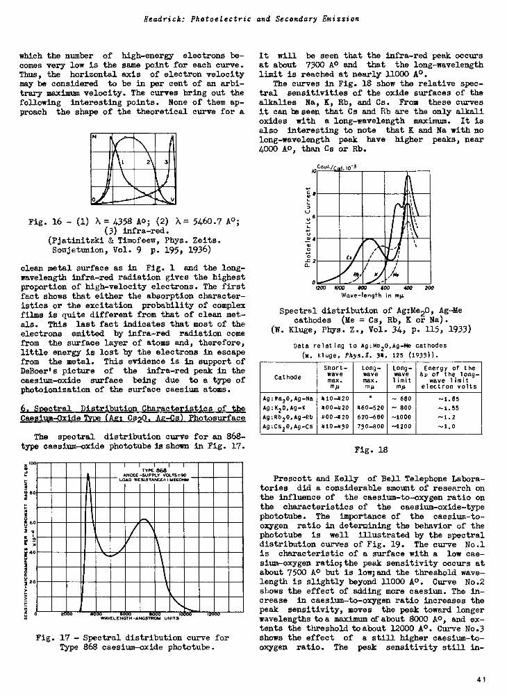
Headrick: Photoelectric and Secondary Emission
which the number of high-energy electrons be-comes very low is the same point for each curve.Thus, the horizontal axis of electron velocitymay be considered to be in per cent of an arbi-trary maximum velocity. The curves bring out thefollowing interesting points. None of them ap-proach the shape of the theoretical curve for a
N
3
0
Fig. 16 - (1) A = 4358 Ao; (2) X= 5460.7 A°;(3) infra -red.
(Pjatinitzki & Timofeew, Phys. Zeita.Sowjetunion, Vol. 9 p. 195, 1936)
clean metal surface as in Fig. 1 and the long -
wavelength infra -red radiation gives the highestproportion of high -velocity electrons. The firstfact shows that either the absorption character-istics or the excitation probability of complexfilms is quite different from that of clean met-als. This last fact indicates that most of theelectrons emitted by infra -red radiation comefrom the surface layer of atoms and, therefore,little energy is lost by the electrons in escapefrom the metal. This evidence is in support ofDeBoerls picture of the infra -red peak in the
caesium -oxide surface being due to a type ofphotoionization of the surface caesium atoms.
6. Spectral Distribution Characteristics of theCaesium -Oxide Type (Ag: C820. Ag-Cs) Photosurface
The spectral distribution curve for an 868 -type caesium -oxide phototube is shown in Fig. 17.
00
$
I !litTYPE 868
ANODE -SUPPLY VOLTS.90LOAD RESISTANCE.' MEGONM
60
60
9I
F,
40
20
0 2600 .46146 (,e A60n i 12E50WAVELENGTH-ANGS UNITS
Fig. 17 - Spectral distribution curve forType 868 caesium -oxide phototube.
It will be seen that the infra -red peak occursat about 7300 A° and that the long -wavelengthlimit is reached at nearly 11000 A°.
The curves in Fig. 18 show the relative spec-tral sensitivities of the oxide surfaces of thealkalies Na, K, Rb, and Cs. From these curvesit can be seen that Cs and Rb are the only alkalioxides with a long -wavelength maximum. It isalso interesting to note that K and Na with nolong -wavelength peak have higher peaks, near4000 Ao, than Cs or Rb.
N8
06
0
0
a
0
Cou1./c01.103
,I1
11
/,1:\
k
Cl
S)/ N 44
200 1000 800 600 *VWave -length in my.
Spectral distribution of Ag:Me20, Ag-Mecathodes (Me = Cs, Rb, K or Na).
(w. Kluge, Phys. Z., Vol. 34, p. 115, 1933)
200
Data relating to Ag:Me20,Ag-Me cathodes
(W. Kluge, Phys.Z. 34, 125 (1933)).
Cathode
Short-wavemax.mµ
Long-wavemax.mµ
Long-wavelimitmµ
Energy of theby of the long -
wave limitelectron volts
Ag:Na20,Ag-Na
Ag:K20,Ag-K
Ag:Rb20,Ag-Rb
Ag:Cs20,Ag-Cs
410-420
400-420
400-420
410-430
.
460-520
620-680
730-800
- 680
- 800
-1000
-1200
-1.85
-1.55
-1.2-1.0
Fig. 18
Prescott and Kelly of Bell Telephone Labora-tories did a considerable amount of research onthe influence of the caesium -to -oxygen ratio onthe characteristics of the caesium -oxide -typephototube. The importance of the caesium -to -
oxygen ratio in determining the behavior of thephototube is well illustrated by the spectraldistribution curves of Fig. 19. The curve No.1is characteristic of a surface with a low cae-sium -oxygen ratio; the peak sensitivity occurs atabout 7500 A° but is low;and the threshold wave-length is slightly beyond 11000 A°. Curve No.2shows the effect of adding more caesium. The in-crease in caesium -to -oxygen ratio increases thepeak sensitivity, moves the peak toward longerwavelengths to a maximum of about 8000 Ao, and ex-tents the threshold to about 12000 A°. Curve No.3shows the effect of a still higher caesium -to -oxygen ratio. The peak sensitivity still in -
41
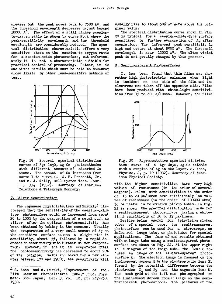
Vacuum Tube Design
creases but the peak moves back to 7500 andthe threshold wavelength decreases tojust beyond10000 A°. The effect of a still higher caesium -to -oxygen ratio is shown by curve No.4 where thepeak -sensitivity wavelength and the thresholdwavelength are considerably reduced. The spec-tral distribution characteristic offers a verysensitive check on the caesium -to -oxygen ratiofor a caesium -oxide photosurface, but unfortun-ately it is not a characteristic suitable forpractical control of processing. Rather, it is
one of the results which must be held to somewhatclose limits by other less -sensitive methods oftest.
3
01000 900 *00 700
Wave -length in mil
Fig. 19 - Several spectral distributioncurves of Ag: Cs20, Ag-Cs photocathodeswith different amounts of adsorbed Csatoms. The amount of Cs increases fromcurve 1 to curve 4. C. H. Prescott, Jr.and M. J. Kelly, Bell System Tech. Jour.11, 334 (1932). Courtesy of AmericanTelephone & Telegraph Company.
7. Silver Sensitization
600
The Japanese physicists,Asao end Suzuki,4 dis-covered that the sensitivity of the caesium -oxidetype photosurface could be increased from about20 to 100% by the evaporation of a metal such assilver after the optimum photosensitivity hasbeen obtained by baking -in the caesium. Usuallythe evaporation of a very small amount of Ag onthe sensitive surface causes a slight rise insensitivity, about 5%, followed by a rapid de-crease in sensitivity with further silver evapora-tion. However, if the Ag is evaporated untilthe photosensitivity has decreased to about 20%of its origimAl value and baked for a few min-utes between 170 and 190°C, the sensitivity will
4 S. Asao and M. Suzuki, "Improvement of ThinFilm Caesium Photoelectric Tube," Proc. Phys.Math. Soc. Japan, Ser. 3, Vol. 12, pp. 247-250;1930.
usually rise to about 50% or more above the ori-ginal value.
The spectral distribution curve shown in Fig.20 is typical for a caesium -oxide -type surfacesensitized by further evaporation of Ag aftercaesiation. The infra -red peak sensitivity ishigh and occurs at about 8500 A°. The thresholdwavelength is near 12000 A°. The ultra -violetpeak is not greatly changed by this process.
8. Semitransparent Photosurfaces
It has been found that thin films may showrather high photoelectric emission when lightis incident on one side of the film and theelectrons are taken off the opposite side. Filmshave been produced with white -light sensitivi-ties from 15 to 40 µa/lumen. However, the films
200
%.000
1200 1000 800 600 400Wave -length in nliA
Fig. 20 - Representative spectral distribu-tion curve of a Ag: Cs20, Ag-Cs cathodewith a surplus of Ag in the layer. S. Asao,Physics, 2, p. 19 (1932). Courtesy of Amer-ican Physical Society.
with the higher sensitivities have very highvalues of resistance (in the order of severalmegohms). Films with sensitivities in the orderof 15 to 20 µa/lumen have sufficiently low val-ues of resistance (in the order of 100000 ohms)to be useful in television pickup tubes. In Fig.21 is shown the spectral distribution curve fora semitransparent photosurface having a white -
light sensitivity of 16 to 17 µa/lumen.Besides being useful for television pickup
tubes of a special type, the semitransparentphotosurface can be used for a microscope, aninfra -red image tube, or phototubes for specialapplications. The form of and results obtainedwith an image tube using a semitransparent photo -surface are shown in Fig. 22. At the upper rightis a diagram of the image tube. The lens 0 fo-cuses an image on the semitransparent photo -
surface K. The electron image is focused on theluminescent screen S by the electrostatic lens E,formed by the potential difference between theelectrodes Zi and Z2 and the magnetic lens M.The mesh grid at the left was photographed on
the luminescent screen from an image on the semi-transparent photocathode. The pictures of the
42
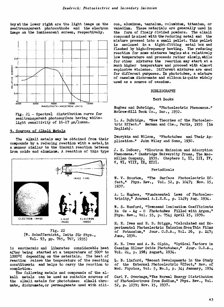
Headrick: Photoelectric and Secondary Emission
boy at the lower right are the light image on thesemitransparent photocathode and the electronimage on the luminescent screen, respectively.
2.0
iS 16cc
0.4
04000 6000 8000 10000 12000
WAVELENGTH - ANGSTROM UNITS
Fig. 21 - Spectral distribution curve forsemitransparent photosurface having white -light sensitivity of 16-17 µa/lumen.
9. Sources of Alkali Metals
The FOlrali metals may be obtained from theircompounds by a reducing reaction with a metal,ina manner similar to the thermit reaction betweeniron oxide and aluminum. A reaction of this type
Fig. 22(W. Schaffernicht, Zeits flir Phys.,
Vol. 93, pp. 765, 767, 1935)
is exothermic and liberates considerable heatafter being started at a temperature of 5000 to10000C depending on the materials. The heat ofreaction raises the temperature of the reactingconstituents and helps to carry the reaction tocompletion.
The following metals and compounds of the al-kali metals can be used as suitable sources ofthe alkAn metals for phototubes: alkali chro-mate, dichromate, or permanganate used with sili-
con, aluminum, tantalum, columbium, titanium, orvanadium. These materials are generally used inthe form of finely divided powders. The alkalicompound is mixed with the reducing metal and the
mixture pressed into a small pellet. This pelletis enclosed in a tight -fitting metal box andflashed by high -frequency heating. The reducingreaction for some mixtures begins at a relativelylow temperature and proceeds rather slowly, whilefor other mixtures the reaction may start at amuch higher temperature and proceed with almostexplosive violence. Different mixtures are usedfor different purposes. In phototubes, a mixtureof caesium dichromate and silicon is quite widelyused as a source of caesium.
BIBLIOGRAPHY
Text Books
Hughes and Dubridge,McGraw-Hill Book Co.,
L. A. DuBridge, "Newtric Effect." HermanEnglish).
"Photoelectric Phenomena."Inc., 1932.
Theories of the Photoelec-and Cie., Paris, 1935 (in
Zworykin and Wilson, "Phototubes and Their Ap-plication." John Wiley and Sons, 1930.
J. H. DeBoer, "Electron Emission and AdsorptionPhenomena." Cambridge University Press, The Mac-millan Company, 1935. Chapters I, II, III, IV,V, VI, VIII, IX, XIII.
Periodicals
W. V. Houston, "The Surface Photoelectric Ef-fect," Phys. Rev., Vol. 52, p. 1047; Nov. 15,
1937.
A. L. Hughes, "Fundamental Laws of Photoelec-tricity," Journal A.I.E.E., p. 1149; Aug. 1934.
W. S. Huxford, "Townsend Ionization CoefficientsIn Cs - Ag - 0 Phototubes Filled with Argon,"Phys. Rev., Vol. 55, p. 754; April 15, 1939.
H. E. Ives and H. B. Briggs, "Calculated and Ex-perimental Photoelectric Emission from Thin Filmsof Potassium," Jour. 0.S.A., Vol. 26, P. 247;June, 1936.
H. E. Ives and A. R. Olpin, "Optical Factors inCaesium Silver Oxide Phototubes," Jour. 0.S.A.,Vol. 24, p. 198; August, 1934.
L. B. Linford, "Recent Developments in the Studyof the External Photoelectric Effect," Rev. ofMod. Physics, Vol. 5, No.1, p. 34; January, 1934
Carl F. Overhage,"The Normal Energy Distributionof Photoelectrons from Sodium," Phys. Rev., Vol.52, p. 1039; Nov. 15, 1937.
43
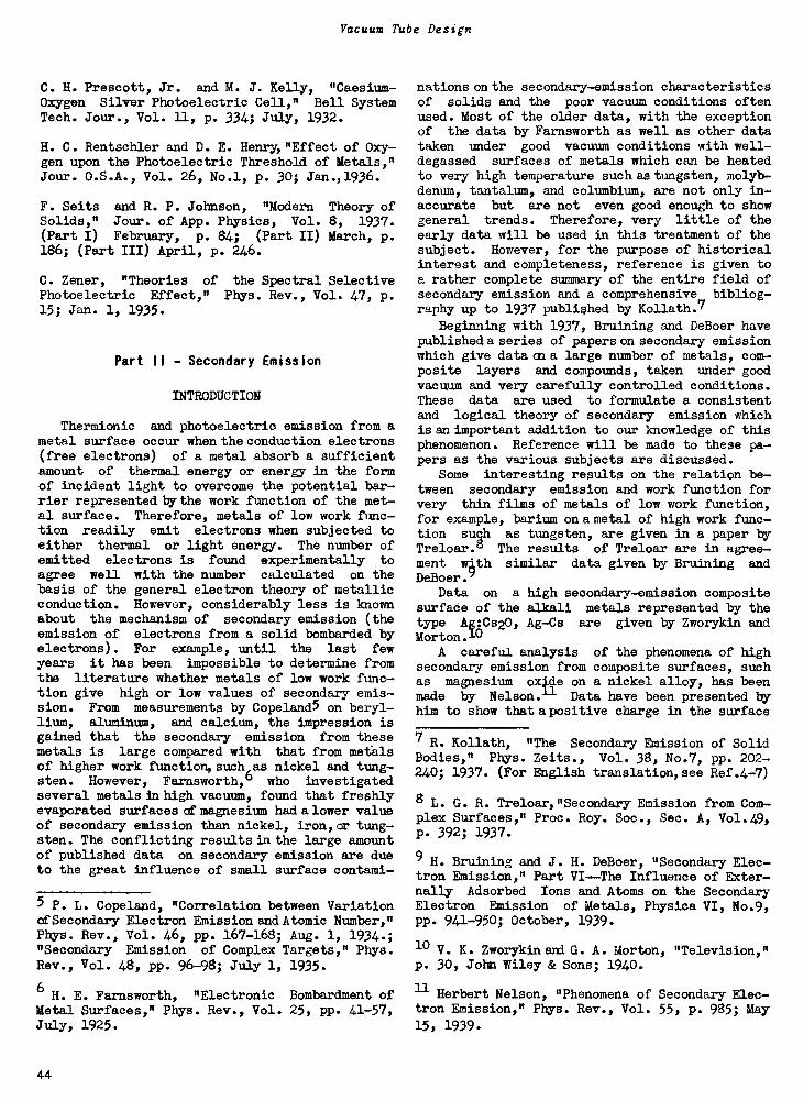
Vacuum Tube Design
C. H. Prescott, Jr. and M. J. Kelly, "Caesium -
Oxygen Silver Photoelectric Cell," Bell SystemTech. Jour., Vol. 11, p. 334; JulY, 1932.
H. C. Rentschler and D. E. Henryi"Effect of Oxy-gen upon the Photoelectric Threshold of Metals,"Jour. O.S.A., Vol. 26, No.1, p. 30; Jan.,1936.
F. Seits and R. P. Johnson, "Modern Theory ofSolids," Jour. of App. Physics, Vol. 8, 1937.(Part I) February, p. 84; (Part II) March, p.186; (Part III) April, p. 246.
C. Zener, "Theories of the Spectral SelectivePhotoelectric Effect," Phys. Rev., Vol. 47, p.15; Jan. 1, 1935.
Part II - Secondary Emission
INTRODUCTION
Thermionic and photoelectric emission from ametal surface occur when the conduction electrons(free electrons) of a metal absorb a sufficientamount of thermal energy or energy in the formof incident light to overcome the potential bar-rier represented by the work function of the met-al surface. Therefore, metals of low work func-tion readily emit electrons when subjected toeither thermal or light energy. The number ofemitted electrons is found experimentally toagree well with the number calculated on thebasis of the general electron theory of metallicconduction. However, considerably less is knownabout the mechanism of secondary emission (theemission of electrons from a solid bombarded byelectrons). For example, until the last fewyears it has been impossible to determine fromthe literature whether metals of low work func-tion give high or low values of secondary emis-sion. From measurements by Copeland5 on beryl-lium, aluminum, and calcium, the impression isgained that the secondary emission from thesemetals is large compared with that from metalsof higher work function, such as nickel and tung-sten. However, Farnsworth,6 who investigatedseveral metals in high vacuum, found that freshlyevaporated surfaces of magnesium had a lower valueof secondary emission than nickel, iron,cr tung-sten. The conflicting results in the large amountof published data on secondary emission are dueto the great influence of small surface contami-
5 P. L. Copeland, "Correlation between Variationof Secondary Electron Emission and Atomic Number,"Phys. Rev., Vol. 46, pp. 167-168; Aug. 1, 1934.;"Secondary Emission of Complex Targets," Phys.Rev., Vol. 48, pp. 96-98; July 1, 1935.
6H. E. Farnsworth, "Electronic Bombardment of
Metal Surfaces," Phys. Rev., Vol. 25, pp. 41-57,July, 1925.
nations on the secondary -emission characteristicsof solids and the poor vacuum conditions oftenused. Most of the older data, with the exceptionof the data by Farnsworth as well as other datataken under good vacuum conditions with well -degassed surfaces of metals which can be heatedto very high temperature such as tungsten, molyb-denum, tantalum, and columbium, are not only in-accurate but are not even good enough to showgeneral trends. Therefore, very little of theearly data will be used in this treatment of thesubject. However, for the purpose of historicalinterest and completeness, reference is given toa rather complete summary of the entire field ofsecondary emission and a comprehensive bibliog-raphy up to 1937 published by Kollath.7
Beginning with 1937, Bruining and DeBoer havepublished a series of papers on secondary emissionwhich give data al a large number of metals, com-posite layers and compounds, taken under goodvacuum and very carefully controlled conditions.These data are used to formulate a consistentand logical theory of secondary emission whichis an important addition to our knowledge of thisphenomenon. Reference will be made to these pa-pers as the various subjects are discussed.
Some interesting results on the relation be-tween secondary emission and work function forvery thin films of metals of low work function,for example, barium on a metal of high work func-tion such as tungsten, are given in a paper byTreloar.8 The results of Treloar are in agree-ment wroth similar data given by Bruining andDeBoer.
Data on a high secondary -emission compositesurface of the alkali metals represented by thetype Ag:Cs20, Ag-Cs are given by Zworykin andMorton...L.°
A careful analysis of the phenomena of highsecondary emission from composite surfaces, suchas magnesium oxide on a nickel alloy, has beenmade by Nelson. Data have been presented byhim to show that a positive charge in the surface
7 R. Kollath, "The Secondary Emission of SolidBodies," Phys. Zeits., Vol. 38, No.7, pp. 202 -240; 1937. (For English translation, see Ref.4-7)
8 L. G. R. Treloar,"Secondary Emission from Com-plex Surfaces," Proc. Roy. Soc., Sec. A, Vol.49,p. 392; 1937.
9 H. Bruining and J. H. DeBoer, "Secondary Elec-tron Emission," Part VI The Influence of Exter-nally Adsorbed Ions and Atoms on the SecondaryElectron Emission of Metals, Physics VI, No.9,pp. 941-950; October, 1939.
10 V. K. Zworykinemd G. A. Morton, "Television,"p. 30, John Wiley & Sons; 1940.
11 Herbert Nelson, "Phenomena of Secondary Elec-tron Emission," Phys. Rev., Vol. 55, p. 985; May
15, 1939.
44
Headrick: Photoelectric and Secondary Emission
film is an important factor contributing to highsecondary emission. He also has pointed out therelation between high secondary emission fromcomposite surfaces and thin-film field emissiondescribed by Malter.12
Data on the secondary -emission characteristicsof insulators, such as glasses and luminescentmaterials, are far less numerous than that onmetals but some results may be found in the fol-lowing references.13,14,15
SECONDARY EMISSION OF CLEAN METALS
The secondary -emission ratio (S = the numberof secondary electrons emitted per bombardingprimary electron) increases to a maximum value,then decreases when the voltage of the primaryelectrons is increased, as shown in Fig. 23 whichgives data on a number of clean metals. A simi-
0
.I
-k.
mammomml
Ell g5o _
25 lir .........-, fl i1/4'
MO MIMMMM=
SO Pr,JIIC,-/- memINIIIIIIIIidKA
-_--=-11r.EMINM
W1111400 _mm
/75
MIIIIIIIIIMMINMN
W II I
T_ ___M-
-/-1,=
- '0 100 20 SOO 46g k4 hoe ko6 I NoPRIMARY -ELECTRON VELOCITY - VOLTS
Fig. 23
(Data from Bruining and DeBoer)
lar type of curve is characteristic of the vari-ation of secondary emission with primary electronvoltage for contaminated or composite surfaces.
12 L. Malter, "Thin -Film Field Emission," Phys.PP 48-58; July 1, 1936.Rev., Vol. 50,
13 W. B. Nottingham, "Electrical and LuminescentProperties of Willemite under Electron Bombard-ment," Jour. of App. Phys., Vol. 8, pp. 762-778;November, 1937.
14 Von C. Hagen and H. Bey, "Charge Potential ofInsulators Bombarded by Electrons," Zeits. f.
Physik, 104, pp. 681-684; 1937.
15 S. T. Martin and L. B. Headrick, "Light Outputand Secondary -Emission Characteristics of Lumin-escent Materials," Jour. of App. Phys., Vol. 10,pp. 116-127; February, 1939.
Data from Bruining and DeBoer16,17 on themaximum value of S for several metals and theprimary electron voltage at which it occurs aregiven in the following table along with data onwork function, atomic weight, and atomic volumefor comparison. It will be noted that, taken asa whole, the data in this table show a lack ofcorrelation of the maximum value of S with workfunction, atomic weight, or atomic volume.
Table I
SECONDARY EMISSION FROM CLEAN METALS
PrimaryMaximum VoltageSecond- at Max- Work
Metal ary imum Func- Atomic Atomic
Emission Emission tion Weight Volume
Ratio (approx.S Volts) (Volts)
Be 0.53 200 3.16 9.0 4.9Li 0.56 83 2.28 6.9 13.0Cs 0.72 400 1.81 132.8 71.0Ba 0.83 400 2.11 137.4 36.1Mg 0.95 200 2.42 24.3 14.1Al 0.97 300 2.26 27.0 10.0Th 1.14 750 3.38 232.2 21.1Ni 1.25 500 5.03 58.7 6.7Mo 1.25 375 4.15 96.0 9.3Cu 1.29 600 4.30 63.6 7.1W 1.35 630 4.54 184.0 9.8Ag 1.56 800 4.74 107.9 10.2
However, upon more critical examination, onefinds that the following generalizations withregard to the secondary -emission characteristicsof different metals are illustrated by the curvesof Fig. 23 and the data in Table I.
1) The maximum value of S occurs at lowervoltages for the light metals than for the heavymetals.
2) The rate of decrease of S with increas-ing primary -electron voltage beyond the maximumis higher for the light metals than for the heavyones.
3) The maximum value of S occurs at highervalues of primary -electron voltage for metals ofhigh work function than for those of low workfunction among metals of similar atomic weight.
16 H. Bruining and J. H. DeBoer -- PreliminaryCommunication: "Secondary Electron Emission ofMetals of Low Work Function," Physica IV, No.6,PP. 473-477; June, 1937.
17 H. Bruining and J. H. DeBoer, "Secondary Elec-tron Emission," Part I --Secondary Emission ofMetals, Physica V, No.1, pp. 17-30; January, 1938;Part II -Absorption of Secondary Electrons, Phys-ica V, No.10, pp. 901-912; December, 1938.
45
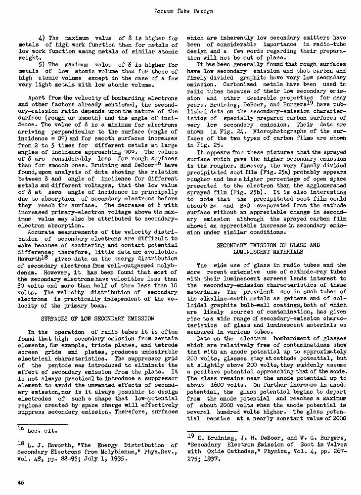
Vacuum Tube Design
4) The maximum value of S is higher formetals of high work function than for metals oflow work function among metals of similar atomicweight.
5) The maximum value of 6 is higher formetals of low atomic volume than for those ofhigh atomic volume except in the case of a fewvery light metals with low atomic volume.
Apart from the velocity of bombarding electronsand other factors already mentioned, the second-ary -emission ratio depends upon the nature of thesurface (rough or smooth) and the angle of inci-dence. The value of 8 is a minimum for electronsarriving perpendicular to the surface (angle ofincidence = 00) and for smooth surfaces increasesfrom 2 to 5 times for different metals at largeangles of incidence approaching 900. The valuesof 8 are considerably less for rough surfacesthan for smooth ones. Bruining and DeBoerl° havefound, upon analysis of data showing the relationbetween 8 and angle of incidence for differentmetals and different voltages, that the low valueof 8 at zero angle of incidence is principallydue to absorption of secondary electrons beforethey reach the surface. The decrease of 8 withincreased primary -electron voltage above the max-imum value may also be attributed to secondary -electron absorption.
Accurate measurements of the velocity distri-bution of secondary electrons are difficult tomake because of scattering and contact potentialdifference; therefore, little data are available.Haworth18 gives data on the energy distributionof secondary electrons Atm well-outgassed molyb-denum. However, it has been found that most ofthe secondary electrons have velocities less than30 volts and more than half of them less than 10volts. The velocity distribution of secondaryelectrons is practically independent of the ve-locity of the primary beam.
SURFACES OF LOW SECONDARY EMISSION
In the operation of radio tubes it is oftenfound that high secondary emission from certainelements, far example, triode plates, and tetrodescreen grids and plates, produces undesirableelectrical characteristics. The suppressor gridof the pentode was introduced to eliminate theeffect of secondary emission from the plate. It
is not always practical to introduce a suppressorelement to avoid the unwanted effects of second-ary emission,nor is it always possible to designelectrodes of such a shape that low -potential
regions created by space charge will effectivelysuppress secondary emission. Therefore, surfaces
16 Loc. cit.
18 L. J. Haworth, "The Energy Distribution ofSecondary Electrons from Molybdenum," Phys.Rev.,
Vol. 48, pp. 88-95; July 1, 1935.
which are inherently low secondary emitters havebeen of considerable importance in radio -tube
design and a few words regarding their prepara-tion will not be out of place.
It has been generally found that rough surfaceshave low secondary emission and that carbon andfinely divided graphite have very low secondaryemission. Carbonized metals have been used in
radio tubes because of their low secondary emis-sion and other desirable properties for manyyears. Bruining, DeBoer, and Burgers19 have pub-lished data on the secondary -emission character-istics of specially prepared carbon surfaces ofvery low secondary emission.. Their data are
shown in Fig. 24. Microphotographs of the sur-faces of the two types of carbon films are shownin Fig. 25.
It appears from these pictures that the sprayedsurface which gave the higher secondary emissionis the rougher. However, the very finely dividedprecipitated soot film (Fig. 25a) probably appearsrougher and has a higher percentage of open spacepresented to the electron than the agglomeratedsprayed film (Fig. 25b). It is also interestingto note that the precipitated soot film couldabsorb Ba and Ba0 evaporated from the cathodesurface without an appreciable change in second-ary emission although the sprayed carbon filmshowed an appreciable increase in secondary emis-sion under similar conditions.
SECONDARY EMISSION OF GLASS ANDLUMINESCENT MATERIALS
The wide use of glass in radio tubes and themore recent extensive use of cathode-ray tubeswith their luminescent screens lends interest tothe secondary -emission characteristics of thesematerials. The prevalent use in such tubes ofthe alkaline -earth metals as getters and of col-loidal graphite bulb -wall coatings, both of whichare likely sources of contamination, has givenrise toa wide range of secondary -emission charac-teristics of glass and luminescent materials asmeasured in various tubes.
Data on the electron bombardment of glasseswhich are relatively free of contaminations showthat with an anode potential up to approximately200 volts, glasses stay at cathode potential, butat slightly above 200 volts, they suddenly assumea positive potential approaching that of the anode.The glass remains near the anode potential up toabout 1600 volts. On further increase in anodepotential, the glass potential begins to departfrom the anode potential and reaches a maximumof about 2000 volts when the anode potential isseveral hundred volts higher. The glass poten-tial remains at a nearly constant value of 2000
19 H. Bruining, J. H. DeBoer, and W. G. Burgers,"Secondary Electron Emission of Soot in Valveswith Oxide Cathodes," Physica, Vol. 4, pp. 267-
275; 1937.
46
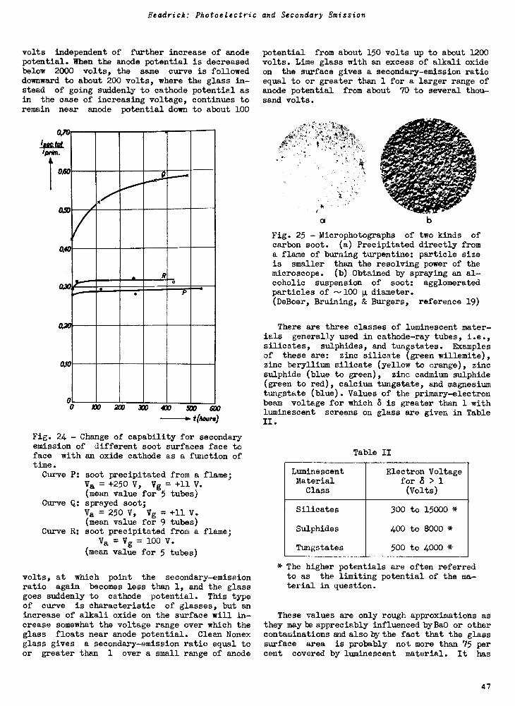
Headrick: Photoelectric and Secondary Emission
volts independent of further increase of anodepotential. When the anode potential is decreasedbelow 2000 volts, the same curve is followeddownward to about 200 volts, where the glass in-stead of going suddenly to cathode potential asin the case of increasing voltage, continues toremain near anode potential down to about 100
;prim
0/0
t.
260
2
410
a3o.
R20
0,10
0
x
..g.--.
R .. P '
0 *Z 270 XV 470 500 600
t(hom40
Fig. 24 - Change of capability for secondaryemission of different soot surfaces face toface with an oxide cathode as a function oftime.
Curve P: soot precipitated from a flame;Va = +250 V, Vg = +11 V.(mean value for 5 tubes)
Curve Q: sprayed soot;Va = 250 V, Vg = +11 V.(mean value for 9 tubes)
Curve R: soot precipitated from a flame;Va = Vg = 100 V.
(mean value for 5 tubes)
volts, at which point the secondary -emissionratio again becomes less than 1, and the glassgoes suddenly to cathode potential. This typeof curve is characteristic of glasses, but anincrease of alkali oxide on the surface will in-crease somewhat the voltage range over which theglass floats near anode potential. Clean Nonexglass gives a secondary -emission ratio equal toor greater than 1 over a small range of anode
potential from about 150 volts up to about 1200volts. Lime glass with an excess of alkali oxideon the surface gives a secondary -emission ratioequal to or greater than 1 for a larger range ofanode potential from about 70 to several thou-sand volts.
a
Fig. 25 - Microphotographs of two kinds ofcarbon soot. (a) Precipitated directly froma flame of burning turpentine: particle sizeis smaller than the resolving power of themicroscope. (b) Obtained by spraying an al-coholic suspension of soot: agglomeratedparticles of --100 11 diameter.(DeBoer, Bruining, & Burgers, reference 19)
There are three classes of luminescent mater-ials generally used in cathode-ray tubes, i.e.,silicates, sulphides, and tungstates. Examplesof these are: zinc silicate (green willemite),zinc beryllium silicate (yellow to orange), zincsulphide (blue to green), zinc cadmium sulphide(green to red), calcium tungetate, and magnesiumtungstate (blue). Values of the primary -electronbeam voltage for which 8 is greater than 1 withluminescent screens on glass are given in TableII.
Table II
LuminescentMaterial
Class
Electron Voltagefor 8 > 1(Volts)
Silicates
Sulphides
Tungstates
300 to 15000 *
400 to 8000 *
500 to 4000 *
* The higher potentials are often referredto as the limiting potential of the ma-terial in question.
These values are only rough approximations asthey may be appreciably influenced byBa0 or othercontaminations and also by the fact that the glasssurface area is probably not more than 75 percent covered by luminescent material. It has
47
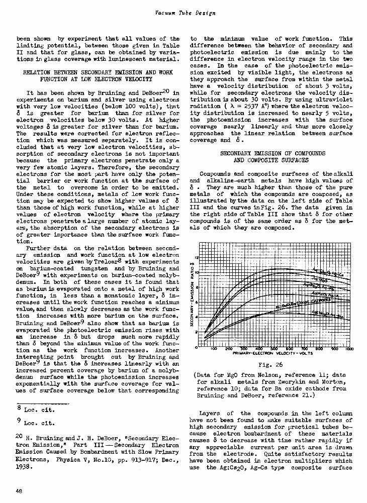
Vacuum Tube Design
been shown by experiment that all values of thelimiting potential, between those given in TableII and that for glass, can be obtained by varia-tions in glass coverage with luminescent material.
RELATION BETWEEN SECONDARY EMISSION AND WORKFUNCTION AT LOW PLECTRON VELOCITY
It has been shown by Bruining and DeBoer2° inexperiments on barium and silver using electronswith very low velocities (below 100 volts), that8 is greater for barium than for silver forelectron velocities below 30 volts. At highervoltages 8 is greater for silver than for barium.The results were corrected for electron reflec-tion which was measured separately. It is con-cluded that at very low electron velocities, ab-sorption of secondary electrons is not importantbecause the primary electrons penetrate only avery few atomic layers. Therefore, the secondaryelectrons for the most part have only the poten-tial barrier or work function at the surface ofthe metal to overcome in order to be emitted.Under these conditions, metals of low work func-tion may be expected to show higher values ofthan those of high work function, while at highervalues of electron velocity where the primaryelectrons penetrate alarge number of atomic lay-ers, the absorption of the secondary electrons isof greater importance than the surface work func-tion.
Further data on the relation between second-ary emission and work function at low electronvelocities are given by Treloar8 with experimentson barium -coated tungsten and by Bruining andDeBoer9 with experiments on barium -coated molyb-denum. In both of these cases it is found thatas barium is evaporated onto a metal of high workfunction, in less than a monatomic layer, 8 in-creases until the work function reaches a minimumvalue, and then slowly decreases as the work func-tion increases with more barium on the surface.
Bruining and DeBoer9 also show that as barium isevaporated the photoelectric emission rises withan increase in 8 but drops much more rapidlythan 8 beyond the minimum value of the work func-tion as the work function increases. Anotherinteresting point brought out by Bruining andDeBoer9 is that the 8 increases linearly with anincreased percent coverage by barium of a molyb-denum surface while the photoemission increasesexponentially with the surface coverage for val-ues of surface coverage below that corresponding
8 Loc. cit.
9 Loc. cit.
20 H. Bruining and J. H. DeBoer, "Secondary Elec-tron Emission," Part III ---Secondary ElectronEmission Caused by Bombardment with Slow PrimaryElectrons, Physica V, No.10, pp. 913-917; Dec.,1938.
to the minimum value of work function. Thisdifference between the behavior of secondary andphotoelectric emission is due mainly to thedifference in electron velocity range in the twocases. In the case of the photoelectric emis-sion excited by visible light, the electrons asthey approach the surface from within the metalhave a velocity distribution of about 3 volts,while for secondary electrons the velocity dis-tribution is about 30 volts. By using ultravioletradiation ( X = 2537 A°) where the electron veloc-ity distribution is increased to nearly 5 volts,the photoemission increases with the surfacecoverage nearly linearly and thus more closelyapproaches the linear relation between surfacecoverage and S.
SECONDARY FMTSSION OF COMPOUNDSAND COMPOSITE SURFACES
Compounds and composite surfaces of the alkaliand alkaline -earth metals have high values of8 . They are much higher than those of the puremetals of which the compounds are composed, asillustrated by the data on the left side of TableIII and the curves in Fig. 26. The data given inthe right side of Table III show that 8 for othercompounds is of the same order as 8 for the met-als of which they are composed.
12
0I-Icc
z0 8N
6-cc
4
MMINIMM MMEMMEMEMMOWI OIMMIMMOMM MICIAMMOMMEMOMOWN INNIMEMMOMMOMM WIMEMEMERINOMMEmEngMEMEMM MENMIIMMEMMENNE MMEMEmMOmmEMBROmmEmffEmmmO111111 11111111111M 11111111111111111111111111MIMEO MOM ME= mumummommummimmum mgMOMMINIMMEMMOMMEMOMO MMMMM
arMINIMMIIMMOMMIIMMIMMEMWM 111222MMERWIRWM41,11111111111111PM01111 1"14111116ftLrAgtNMIIMMMMM 1111 MMNIAM,%diiIMEIMMIIIIII:frpregaMEM= mmg 1,,ipmeopmLAII._ _.4."4.2,..,,m.
IIIIIIIIIImprill rigirile"immomeiM r M rommuommIllimmmumreatommilm -.2....worwazorgim
um yommmv. mm mmr_:1110emsgeppippicromIII IIMAIIIPIAIIIIIIWPWV,(11A1:1-TamaimmilMii
IIllmailmitalillillideitaillirepilliimill
il rildiiIIIPPliiiiiiiiiIIIIIIIIIIiiiigiiA a.mfm.--2-46 mom mom
Im rAOramplr.&11 1 iimm mmmmmm nag milililliii ilma 4,141!nams_. mummommomm.
I 0011 III IIIIIIIIIIIIII IIIIIIIIIII i11Lagraill milummsnmermallmulluilum ..1
200 300 4 500 00 700 - PRIMARY -ELECTRON VELOCITY- VOL TS
Fig. 26
(Data for Mg0 from Nelson, reference 11; datafor alkali metals from Zworykin and Morton,reference 10; data for Ba oxide cathode fromBruining and DeBoer, reference 21.)
Layers of the compounds in the left columnhave not been found to make suitable surfaces ofhigh secondary emission for practical tubes be-cause electron bombardment of these materialscauses 8 to decrease with time rather rapidly ifany appreciable current per unit area is drawnfrom the electrode. Quite satisfactory resultshave been obtained in electron multipliers whichuse the Ag:Cs20, Ag-Cs type composite surface
48
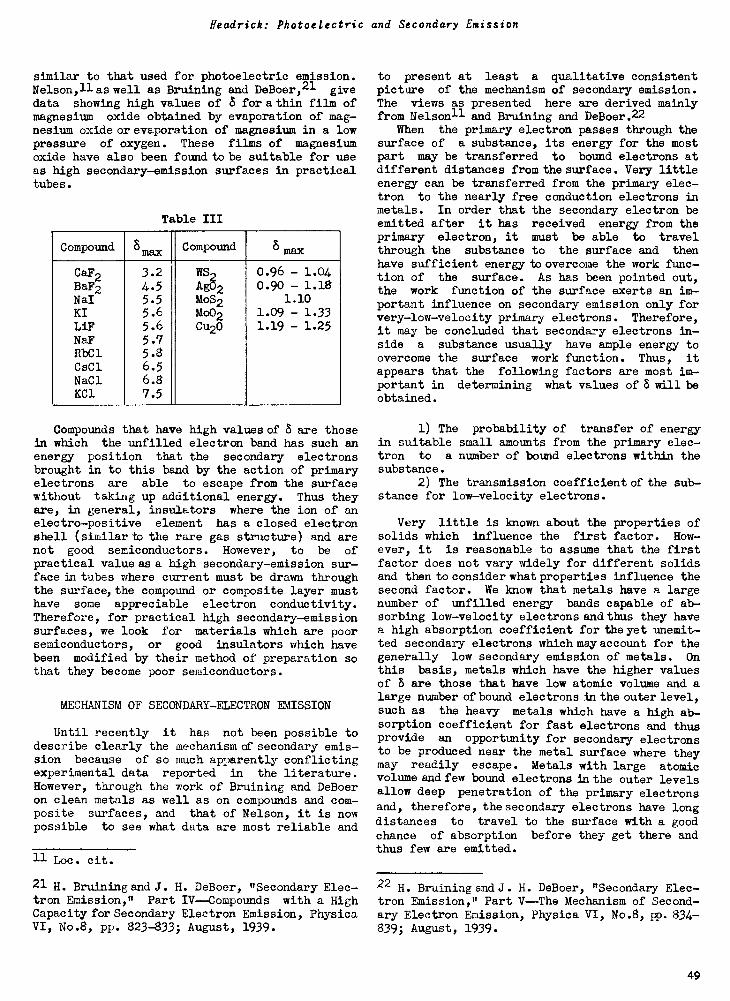
Headrick: Photoelectric and Secondary Emission
similar to that used for photoelectric emission.Nelson,ll as well as Bruining and DeBoer,21 give
data showing high values of 6 for a thin film ofmagnesium oxide obtained by evaporation of mag-nesium oxide or evaporation of magnesium in a lowpressure of oxygen. These films of magnesiumoxide have also been found to be suitable for useas high secondary -emission surfaces in practicaltubes.
Table III
Compound 8 Compound 6 max
CaF2 3.2 WS 0.96 - 1.04BaF2 4.5 Ag02 0.90 - 1.18NaI 5.5 MoS2 1.10KI 5.6 Mo02 1.09 - 1.33
LiF 5.6 Cu20 1.19 - 1.25NaF 5.7Rbel 5.8
CsC1 6.5
NaCl 6.8
KC1 7.5
Compounds that have high values of 6 are thosein which the unfilled electron band has such anenergy position that the secondary electronsbrought in to this band by the action of primaryelectrons are able to escape from the surfacewithout taking up additional energy. Thus theyare, in general, insulators where the ion of anelectro -positive element has a closed electronshell (similar to the rare gas structure) and arenot good semiconductors. However, to be ofpractical value as a high secondary -emission sur-face in tubes where current must be drawn throughthe surface, the compound or composite layer musthave some appreciable electron conductivity.Therefore, for practical high secondary -emissionsurfaces, we look for materials which are poorsemiconductors, or good insulators which havebeen modified by their method of preparation sothat they become poor semiconductors.
MECHANISM OF SECONDARY -ELECTRON EMISSION
Until recently it has not been possible todescribe clearly the mechanism of secondary emis-sion because of so much apparently conflictingexperimental data reported in the literature.However, through the work of Bruining and DeBoeron clean metals as well as on compounds and com-posite surfaces, and that of Nelson, it is nowpossible to see what data are most reliable and
11 Loc. cit.
21 H. Bruining and J. H. DeBoer, "Secondary Elec-tron Emission," Part IV-Compounds with a HighCapacity for Secondary Electron Emission, PhysicaVI, No.8, pp. 823-833; August, 1939.
to present at least a qualitative consistentpicture of the mechanism of secondary emission.The views as presented here are derived mainlyfrom Nelsonll and Bruining and DeBoer.22
When the primary electron passes through thesurface of a substance, its energy for the mostpart may be transferred to bound electrons atdifferent distances from the surface. Very littleenergy can be transferred from the primary elec-tron to the nearly free conduction electrons inmetals. In order that the secondary electron beemitted after it has received energy from theprimary electron, it must be able to travelthrough the substance to the surface and thenhave sufficient energy to overcome the work func-tion of the surface. As has been pointed out,the work function of the surface exerts an im-portant influence on secondary emission only forvery -low -velocity primary electrons. Therefore,it may be concluded that secondary electrons in-side a substance usually have ample energy toovercome the surface work function. Thus, itappears that the following factors are most im-portant in determining what values of 8 will beobtained.
1) The probability of transfer of energyin suitable small amounts from the primary elec-tron to a number of bound electrons within thesubstance.
2) The transmission coefficient of the sub-stance for low -velocity electrons.
Very little is known about the properties ofsolids which influence the first factor. How-ever, it is reasonable to assume that the firstfactor does not vary widely for different solidsand then to consider what properties influence thesecond factor. We know that metals have a largenumber of unfilled energy bands capable of ab-sorbing low -velocity electrons and thus they havea high absorption coefficient for the yet unemit-ted secondary electrons whichmayaccount for thegenerally low secondary emission of metals. Onthis basis, metals which have the higher valuesof 8 are those that have low atomic volume and alarge number of bound electrons in the outer level,such as the heavy metals which have a high ab-sorption coefficient for fast electrons and thusprovide an opportunity for secondary electronsto be produced near the metal surface where theymay readily escape. Metals with large atomicvolume and few bound electrons in the outer levelsallow deep penetration of the primary electronsand, therefore, the secondary electrons have long
distances to travel to the surface with a goodchance of absorption before they get there andthus few are emitted.
22 H. BruiningmadJ. H. DeBoer, "Secondary Elec-tron Emission," Part V --The Mechanism of Second-ary Electron Emission, Physica VI, No.8, pp. 834-839; August, 1939.
49
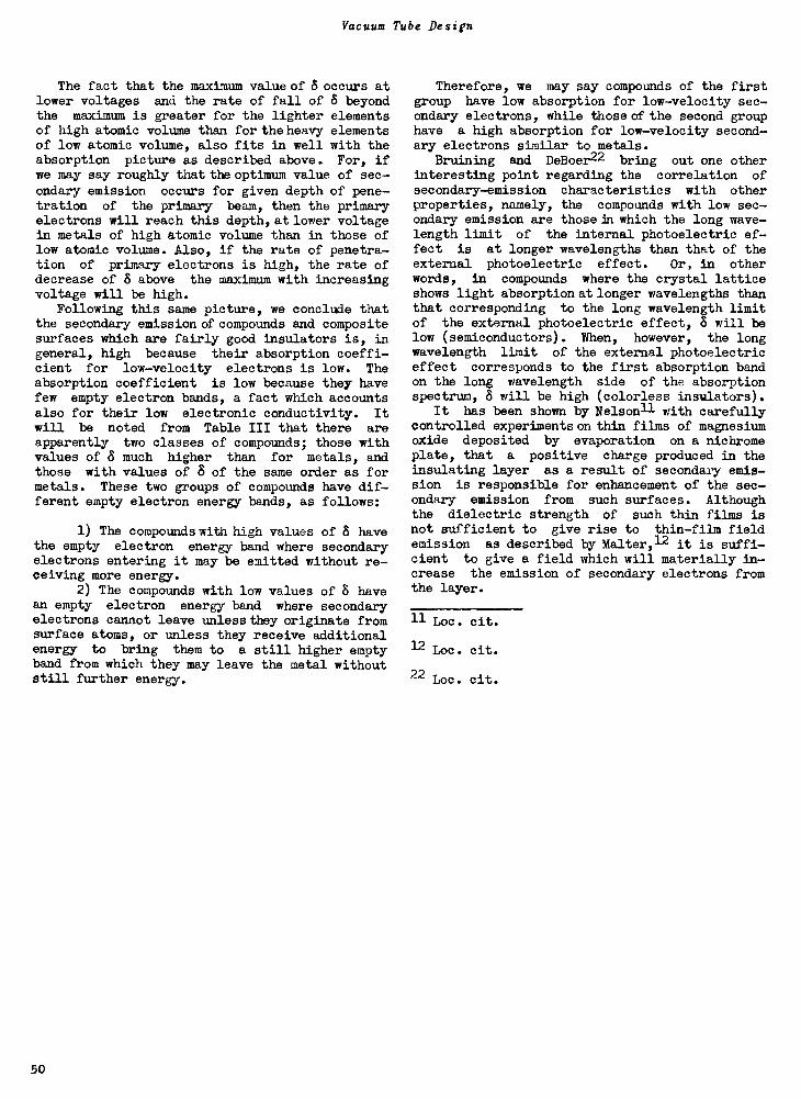
Vacuum Tube Design
The fact that the maximum value of 8 occurs atlower voltages and the rate of fall of 8 beyondthe maximum is greater for the lighter elementsof high atomic volume than for the heavy elementsof low atomic volume, also fits in well with theabsorption picture as described above. For, ifwe may say roughly that the optimum value of sec-
ondary emission occurs for given depth of pene-tration of the primary beam, then the primaryelectrons will reach this depth, at lower voltagein metals of high atomic volume than in those oflow atomic volume. Also, if the rate of penetra-tion of primary electrons is high, the rate ofdecrease of 8 above the maximum with increasingvoltage will be high.
Following this same picture, we conclude thatthe secondary emission of compounds and compositesurfaces which are fairly good insulators is, ingeneral, high because their absorption coeffi-cient for low -velocity electrons is low. Theabsorption coefficient is low because they havefew empty electron bands, a fact which accountsalso for their low electronic conductivity. Itwill be noted from Table III that there areapparently two classes of compounds; those withvalues of 6 much higher than for metals, andthose with values of 8 of the same order as formetals. These two groups of compounds have dif-ferent empty electron energy bands, as follows:
1) The compounds with high values of 6 havethe empty electron energy band where secondaryelectrons entering it may be emitted without re-ceiving more energy.
2) The compounds with low values of 8 havean empty electron energy band where secondaryelectrons cannot leave unless they originate fromsurface atoms, or unless they receive additionalenergy to bring them to a still higher emptyband from which they may leave the metal withoutstill further energy.
Therefore, we may say compounds of the firstgroup have low absorption for low -velocity sec-ondary electrons, while those of the second grouphave a high absorption for low -velocity second-ary electrons similar to metals.
Bruining and DeBoer22 bring out one otherinteresting point regarding the correlation ofsecondary -emission characteristics with otherproperties, namely, the compounds with low sec-ondary emission are those in which the long wave-length limit of the internal photoelectric ef-fect is at longer wavelengths than that of theexternal photoelectric effect. Or, in otherwords, in compounds where the crystal latticeshows light absorption at longer wavelengths thanthat corresponding to the long wavelength limitof the external photoelectric effect, 8 will below (semiconductors). When, however, the longwavelength limit of the external photoelectriceffect corresponds to the first absorption bandon the long wavelength side of the absorptionspectrum, 8 will be high (colorless insulators).
It has been shown by Nelsonll with carefullycontrolled experiments on thin films of magnesiumoxide deposited by evaporation on a nichromsplate, that a positive charge produced in theinsulating layer as a result of secondary emis-sion is responsible for enhancement of the sec-ondary emission from such surfaces. Althoughthe dielectric strength of such thin films isnot sufficient to give rise to thin-film fieldemission as described by Malter,12 it is suffi-cient to give a field which will materially in-crease the emission of secondary electrons fromthe layer.
11 Loc. cit.
12 Loc. cit.
22 Loc. cit.
50
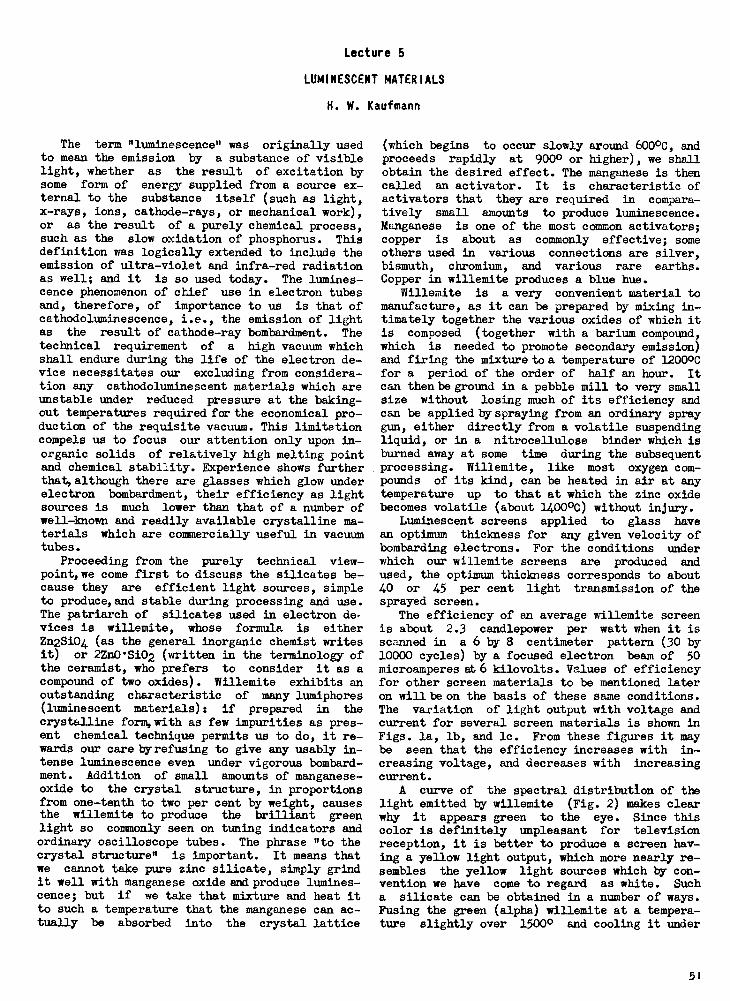
Lecture 5
LUMINESCENT MATERIALS
H. W. Kaufmann
The term "luminescence" was originally usedto mean the emission by a substance of visiblelight, whether as the result of excitation bysome form of energy supplied from a source ex-ternal to the substance itself (such as light,x-rays, ions, cathode -rays, or mechanical work),or as the result of a purely chemical process,such as the slow oxidation of phosphorus. Thisdefinition was logically extended to include theemission of ultra -violet and infra -red radiationas well; and it is so used today. The lumines-cence phenomenon of chief use in electron tubesand, therefore, of importance to us is that ofcathodoluminescence, i.e., the emission of lightas the result of cathode-ray bombardment. Thetechnical requirement of a high vacuum whichshall endure during the life of the electron de-vice necessitates our excluding from considera-tion any cathodoluminescent materials which areunstable under reduced pressure at the baking -out temperatures required for the economical pro-duction of the requisite vacuum. This limitationcompels us to focus our attention only upon in-organic solids of relatively high melting pointand chemical stability. Experience shows furtherthat, although there are glasses which glow underelectron bombardment, their efficiency as lightsources is much lower than that of a number ofwell-known and readily available crystalline ma-terials which are commercially useful in vacuumtubes.
Proceeding from the purely technical view-point, we come first to discuss the silicates be-cause they are efficient light sources, simpleto produce, and stable during processing and use.The patriarch of silicates used in electron de-vices is willemite, whose formula is eitherZn2SiO4 (as the general inorganic chemist writesit) or 2Zn0Si02 (written in the terminology ofthe ceramist, who prefers to consider it as acompound of two oxides). Willemite exhibits anoutstanding characteristic of many lumiphores(luminescent materials): if prepared in thecrystalline form, with as few impurities as pres-ent chemical technique permits us to do, it re-wards our care by refusing to give any usably in-tense luminescence even under vigorous bombard-ment. Addition of small amounts of manganese -oxide to the crystal structure, in proportionsfrom one -tenth to two per cent by weight, causesthe willemite to produce the brilliant greenlight so commonly seen on tuning indicators andordinary oscilloscope tubes. The phrase "to thecrystal structure" is important. It means thatwe cannot take pure zinc silicate, simply grindit well with manganese oxide and produce lumines-cence; but if we take that mixture and heat itto such a temperature that the manganese can ac-tually be absorbed into the crystal lattice
(which begins to occur slowly around 600°C, andproceeds rapidly at 9000 or higher), we shallobtain the desired effect. The manganese is thencalled an activator. It is characteristic ofactivators that they are required in compara-tively small amounts to produce luminescence.Manganese is one of the most common activators;copper is about as commonly effective; someothers used in various connections are silver,bismuth, chromium, and various rare earths.Copper in willemite produces a blue hue.
Willemite is a very convenient material tomanufacture, as it can be prepared by mixing in-timately together the various oxides of which itis composed (together with a barium compound,which is needed to promote secondary emission)and firing the mixture to a temperature of 1200°Cfor a period of the order of half an hour. Itcan then be ground in a pebble mill to very smallsize without losing much of its efficiency andcan be applied by spraying from an ordinary spraygun, either directly from a volatile suspendingliquid, or in a nitrocellulose binder which isburned away at some time during the subsequentprocessing. Willemite, like most oxygen com-pounds of its kind, can be heated in air at anytemperature up to that at which the zinc oxidebecomes volatile (about 1400°C) without injury.
Luminescent screens applied to glass havean optimum thickness for any given velocity ofbombarding electrons. For the conditions underwhich our willemite screens are produced andused, the optimum thickness corresponds to about
40 or 45 per cent light transmission of thesprayed screen.
The efficiency of an average willemite screenis about 2.3 candlepower per watt when it isscanned in a 6 by 8 centimeter pattern (30 by10000 cycles) by a focused electron beam of 50
microamperes at 6 kilovolts. Values of efficiencyfor other screen materials to be mentioned lateron will be on the basis of these same conditions.The variation of light output with voltage andcurrent for several screen materials is shown inFigs. la, lb, and lc. From these figures it maybe seen that the efficiency increases with in-creasing voltage, and decreases with increasingcurrent.
A curve of the spectral distribution of thelight emitted by willemite (Fig. 2) makes clearwhy it appears green to the eye. Since thiscolor is definitely unpleasant for televisionreception, it is better to produce a screen hav-ing a yellow light output, which more nearly re-sembles the yellow light sources which by con-vention we have come to regard as white. Sucha silicate can be obtained in a number of ways.Fusing the green (alpha) willemite at a tempera-ture slightly over 1500° and cooling it under
5I
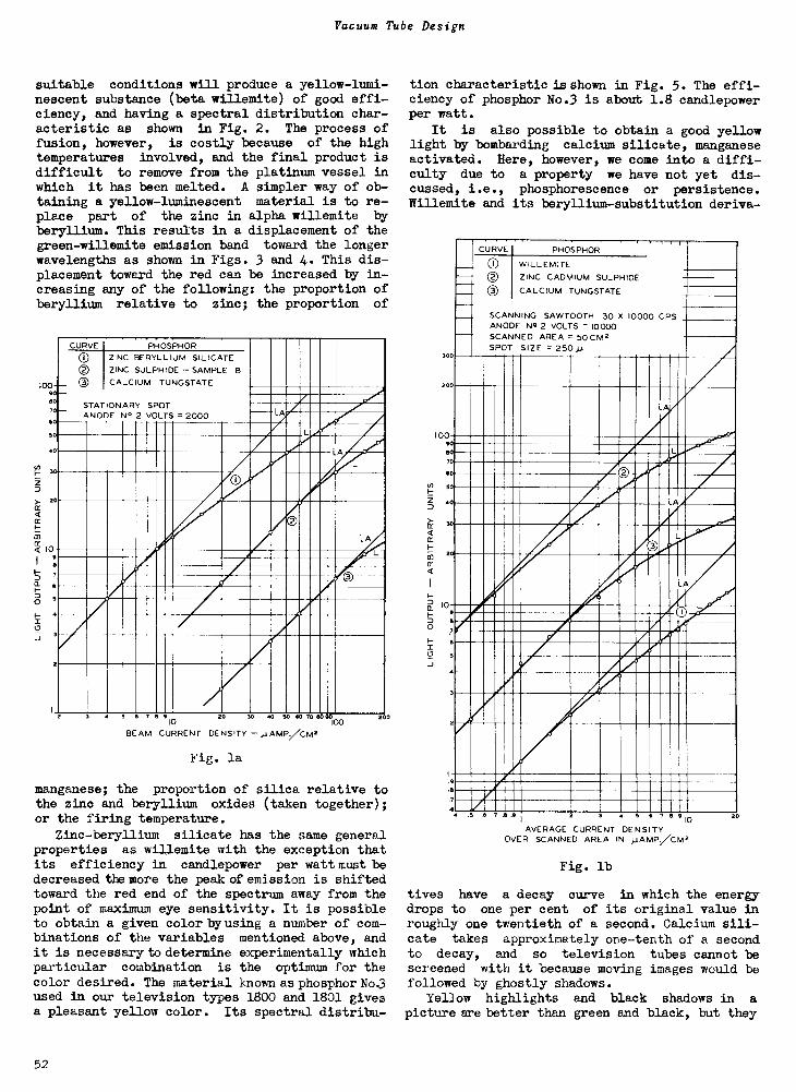
Vacuum Tube Design
suitable conditions will produce a yellow -lumi-nescent substance (beta willemite) of good effi-ciency, and having a spectral distribution char-acteristic as shown in Fig. 2. The process offusion, however, is costly because of the hightemperatures involved, and the final product isdifficult to remove from the platinum vessel inwhich it has been melted. A simpler way of ob-taining a yellow -luminescent material is to re-place part of the zinc in alpha willemite byberyllium. This results in a displacement of thegreen-willemite emission band toward the longerwavelengths as shown in Figs. 3 and 4. This dis-placement toward the red can be increased by in-creasing any of the following: the proportion ofberyllium relative to zinc; the proportion of
10090
SO
70
GO
90
40
CURVE PHOSPHORC)
0g
- STATANODE
ZINC BERYLLIUM SILICATEZINC SULPHIDE - SAMPLE BCALCIUM TUNGSTATE
ONARY SPOTNs 2 VOLTS = 2000 LA
LA
oLA
L
C)
2 5 6 7 8 9 20 30 40 50 60 70 e000100
BEAM CURRENT DENSITY -,u AMP/CM2
Fig. la
200
manganese; the proportion of silica relative tothe zinc and beryllium oxides (taken together);or the firing temperature.
Zinc -beryllium silicate has the same generalproperties as willemite with the exception thatits efficiency in candlepower per watt must bedecreased the more the peak of emission is shiftedtoward the red end of the spectrum away from thepoint of maximum eye sensitivity. It is possibleto obtain a given color by using a number of com-binations of the variables mentioned above, andit is necessary to determine experimentally whichparticular combination is the optimum for thecolor desired. The material known as phosphor No.3used in our television types 1800 and 1801 givesa pleasant yellow color. Its spectral distribu-
tion characteristic is shown in Fig. 5. The effi-ciency of phosphor No.3 is about 1.8 candlepowerper watt.
It is also possible to obtain a good yellowlight by bombarding calcium silicate, manganeseactivated. Here, however, we come into a diffi-culty due to a property we have not yet dis-cussed, i.e., phosphorescence or persistence.Willemite and its beryllium -substitution deriva-
07
z
300
200
100906070
60
50
40
CURVE PHOSPHOR
0 WILLEMITE0 ZINC CADMIUM SULPHIDE® CALCIUM TUNGSTATE
SCANNING SAWTOOTH 30 X 10000 CPSANODE NO 2 VOLTS = 10000SCANNED AREA - 50 CM2SPOT SIZE = 250y A
111
PO111111 PIIIIIIPI
IIIHI mr:di prim.
Ili 441111 L=FAM1111111111111111111111110IIM=111111MMF
Cl)
"IA1
r
20
10
3
2 3 5 6 7 6 9
AVERAGE CURRENT DENSITYOVER SCANNED AREA IN .µAMP/CM2
Fig. lb
20
tives have a decay curve in which the energydrops to one per cent of its original value inroughly one twentieth of a second. Calcium sili-cate takes approximately one -tenth of a secondto decay, and so television tubes cannot bescreened with it because moving images would befollowed by ghostly shadows.
Yellow highlights and black shadows in apicture are better than green and black, but they
52
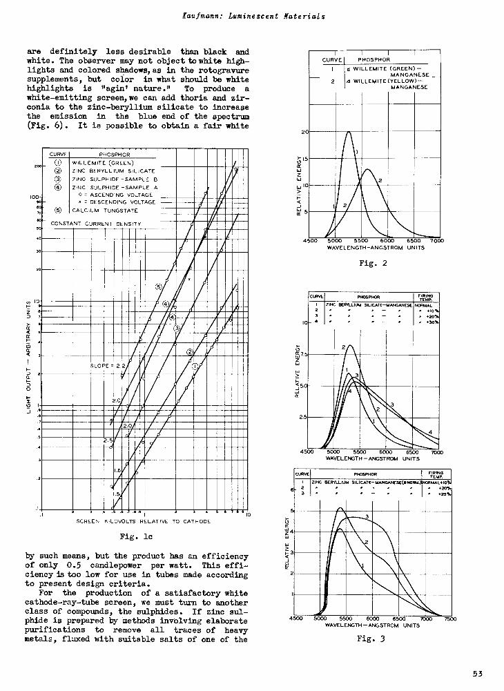
Kaufmann: Luminescent Materials
are definitely less desirable than black andwhite. The observer may not object to white high-lights and colored shadows, as in the rotogravuresupplements, but color in what should be whitehighlights is "agini nature." To produce a
white -emitting screen, we can add thoria and zir-conia to the zinc -beryllium silicate to increasethe emission in the blue end of the spectrum(Fig. 6). It is possible to obtain a fair white
100
CURVE PHOSPHOR
_ 0 WILLEMITE (GREEN)0®®
ZINC BERYLLIUM SILICATEZINC SULPHIDE -SAMPLE BZINC SULPHIDE -SAMPLE A
0 = ASCENDING VOLTAGE- x = DESCENDING VOLTAGE
_ © CALCIUM TUNGSTATE
CONSTANT CURRENT DENSITY /J
/0
r .
O .
SLOPE = 2.2.O
2.0
A.
2.0
2.5 o .
.1.6
'
.
1.5
50
3
20
10I.-
Z a7
3
.4
.5
3 S 6 7 6 610
SCREEN KILOVOLTS RELATIVE TO CATHODE
Fig. lc
by such means, but the product has an efficiencyof only 0.5 candlepower per watt. This effi-ciency is too low for use in tubes made accordingto present design criteria.
For the production of a satisfactory whitecathode -ray -tube screen, we must turn to anotherclass of compounds, the sulphides. If zinc sul-phide is prepared by methods involving elaboratepurifications to remove all traces of heavymetals, fluxed with suitable salts of one of the
6
Z4
3
2
2
015X
Li 10
m 5
I
CURVEI I I
PHOSPHOR
I a WILLEMITE (GREEN) -MA NG AN ESE
2 4 WILLEMITE (YELLOW)-MANGANESE
1
2
1
,
4500 5000 5500 6000 6500 7000WAVELENGTH -ANGSTROM UNITS
2.
Fig. 2
CURVE PHOSPHOR FIRINGTEMP
I
23
ZINC
.
.
BERYLLIUM.
-
2
SILICATE-MANGANESE. --- -
.
.-
NORMAL+10%
- +20%. +30%
31
3
4
4500 5000 5500 6000 6500 7000WAVELENGTH - ANGSTROM UNITS
CURVE PHOSPHOR FIRINGTEMP.
I
23
ZINC.
BERYLLIUM."
SILICATE-."
MANGANESEONORM.-- "
NORMAL+10%. +20%
+25%
3
4500 5000 5500 6000 6500 7000WAVELENGTH - ANGSTROM UNITS
Fig. 3
7500
53
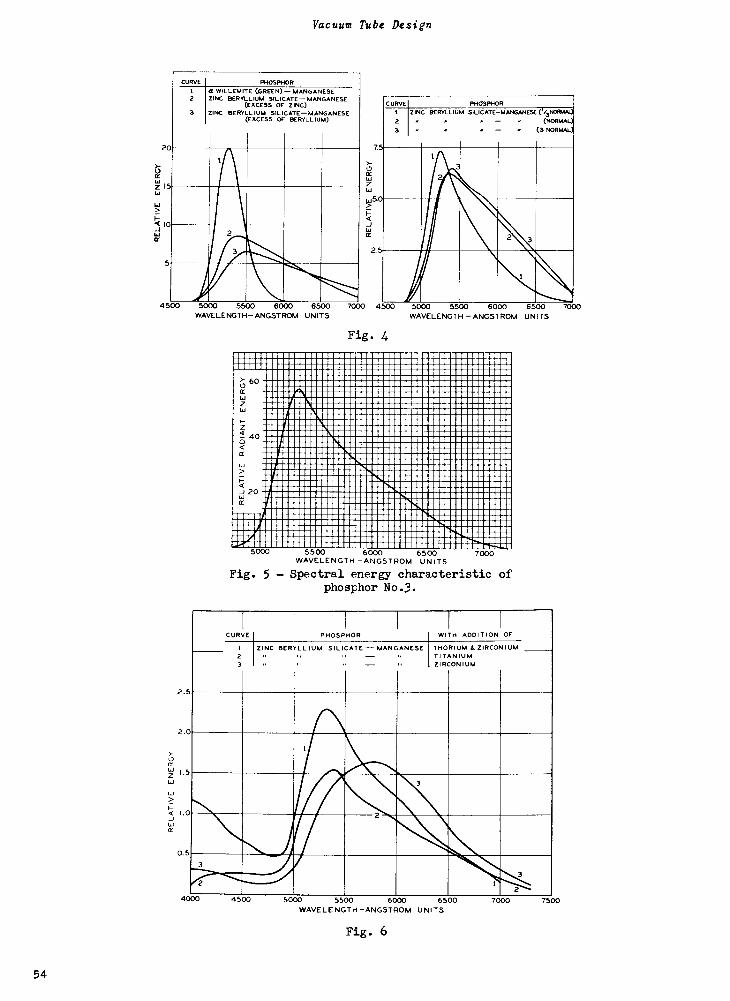
Vacuum Tube Design
CURVE PHOSPHOR
1
2
3
.1 WILLEMITE (GREEN)- MANGANESEZINC BERYLLIUM SILICATE-MANGANESE
(EXCESS OF ZINC)ZINC BERYLLIUM SILICATE-MANGANESE
(EXCESS OF BERYLLIUM)
1
I
irli
2 7.
>-
LUZI
I
CC
5
4500 5000 5500 6000 6500
2.5
2.
0.5
WAVELENGTH-ANGSTROM UNITS
CURVE PHOSPHORI2
3
ZINC
.
.
BERYLLIUM
.
SILICATE-MANGANESE
.--
0/3NORMA0
(NORMAL)(3 NORMAL)
ilb
/\i7000 4500
Fig 4
5000 5500 6000 6500WAVELENGTH -ANGSTROM UNITS
060cc
5 40
420
tJJ
MILOWOOS5000 5500 6000 6500
1111011110711000OM
WAVELENGTH -ANGSTROM UNITS
Fig. 5 - Spectral energy characteristic ofphosphor No.3.
CURVE PHOSPHORr I
WITH ADDITION OF
I ZINC BERYLLIUM
.,
SILICATE - MANGANESE-THORIUMTITANIUMZIRCONIUM
& ZIRCONIUM23
3
'.........-- 1
24000 4500 5000 5500 6000 6500
WAVELENGTH-ANGSTROM UNITS
Fig. 6
7000 7500
7000
54
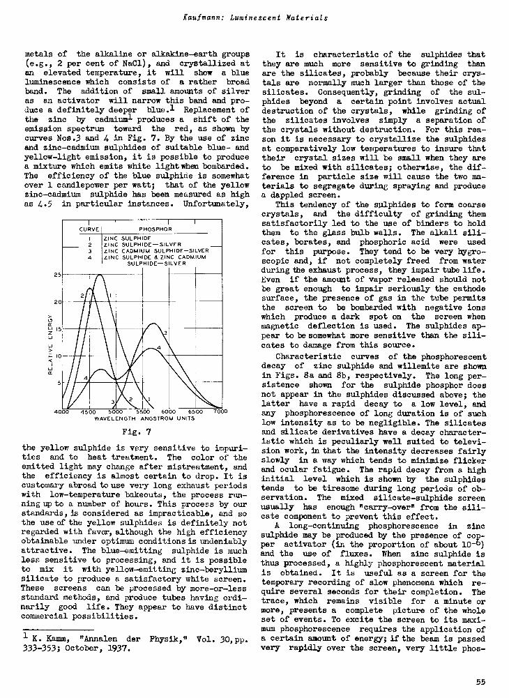
Kaufmann: Luminescent Materials
metals of the alkaline or alkaline -earth groups(e.g., 2 per cent of NaC1), and crystallized atan elevated temperature, it will show a blueluminescence which consists of a rather broadband. The addition of small amounts of silveras an activator will narrow this band and pro-duce a definitely deeper blue.1 Replacement ofthe zinc by cadmiuml produces a shift of theemission spectrum toward the red, as shown bycurves Nos.3 and 4 in Fig. 7. By the use of zincand zinc -cadmium sulphides of suitable blue- andyellow -light emission, it is possible to producea mixture which emits white light when bombarded.The efficiency of the blue sulphide is somewhatover 1 candlepower per watt; that of the yellowzinc -cadmium sulphide has been measured as highas 4.5 in particular instances. Unfortunately,
25
20
CURVEI I
PHOSPHOR
I
234
ZINCZINCZINCZINC
SULPHIDESULPHIDE-SILVERCADMIUMSULPHIDE
SULPHIDE-SILVER
SULPHIDE-SILVER8. ZINC CADMIUM
_
iIirt
1 Avi \
\N...4000 4500 5000 5500 6000 6500 7000
WAVELENGTH -ANGSTROM UNITS
Fig. 7
the yellow sulphide is very sensitive to impuri-ties and to heat treatment. The color of theemitted light may change after mistreatment, andthe efficiency is almost certain to drop. It iscustomary abroad to use very long exhaust periodswith low -temperature bakeouts, the process run-ning up to a number of hours. This process by ourstandards, is considered as impracticable, and sothe use of the yellow sulphides is definitely notregarded with fairer, although the high efficiencyobtainable under optimum conditions is undeniablyattractive. The blue -emitting sulphide is muchless sensitive to processing, and it is possibleto mix it with yellow -emitting zinc -berylliumsilicate to produce a satisfactory white screen.These screens can be processed by more -or -lessstandard methods, and produce tubes having ordi-narily good life. They appear to have distinctcommercial possibilities.
1 K. Kamm, "Annalen der Physik," Vol. 30,pp.333-353; October, 1937.
It is characteristic of the sulphides thatthey are much more sensitive to grinding thanare the silicates, probably because their crys-tals are normally much larger than those of thesilicates. Consequently, grinding of the sul-phides beyond a certain point involves actualdestruction of the crystals, while grinding ofthe silicates involves simply a separation ofthe crystals without destruction. For this rea-son it is necessary to crystallize the sulphidesat comparatively low temperatures to insure thattheir crystal sizes will be small when they areto be mixed with silicates; otherwise, the dif-ference in particle size will cause the two ma-terials to segregate during spraying and producea dappled screen.
This tendency of the sulphides to form coarsecrystals, and the difficulty of grinding themsatisfactorily led to the use of binders to holdthem to the glass bulb walls. The alkali sili-cates, borates, and phosphoric acid were usedfor this purpose. They tend to be very hygro-scopic and, if not completely freed from waterduring the exhaust process, they impair tube life.Even if the amount of vapor released should notbe great enough to impair seriously the cathodesurface, the presence of gas in the tube permitsthe screen to be bombarded with negative ionswhich produce a dark spot on the screen whenmagnetic deflection is used. The sulphides ap-pear to be somewhat more sensitive than the sili-cates to damage from this source.
Characteristic curves of the phosphorescentdecay of zinc sulphide and willemite are shownin Figs. 8a and 8b, respectively. The long per-sistence shown for the sulphide phosphor doesnot appear in the sulphides discussed above; thelatter have a rapid decay to a low level, andany phosphorescence of long duration is of suchlow intensity as to be negligible. The silicatesand silicate derivatives have a decay character-istic which is peculiarly well suited to televi-sion work, in that the intensity decreases fairlyslowly in a way which tends to minimize flickerand ocular fatigue. The rapid decay from a highinitial level which is shown by the sulphidestends to be tiresome during long periods of ob-servation. The mixed silicate -sulphide screenusually has enough "carry-over" from the sili-cate component to prevent this effect.
A long -continuing phosphorescence in zincsulphide may be produced by the presence of cop-per activator (in the proportion of about 10-0)and the use of fluxes. When zinc sulphide isthus processed, a highly phosphorescent materialis obtained. It is useful as a screen for thetemporary recording of slow phenomena which re-quire several seconds for their completion. Thetrace, which remains visible for a minute ormore, presents a complete picture of the wholeset of events. To excite the screen to its maxi-mum phosphorescence requires the application ofa certain amount of energy; if the beam is passedvery rapidly over the screen, very little phos-
55
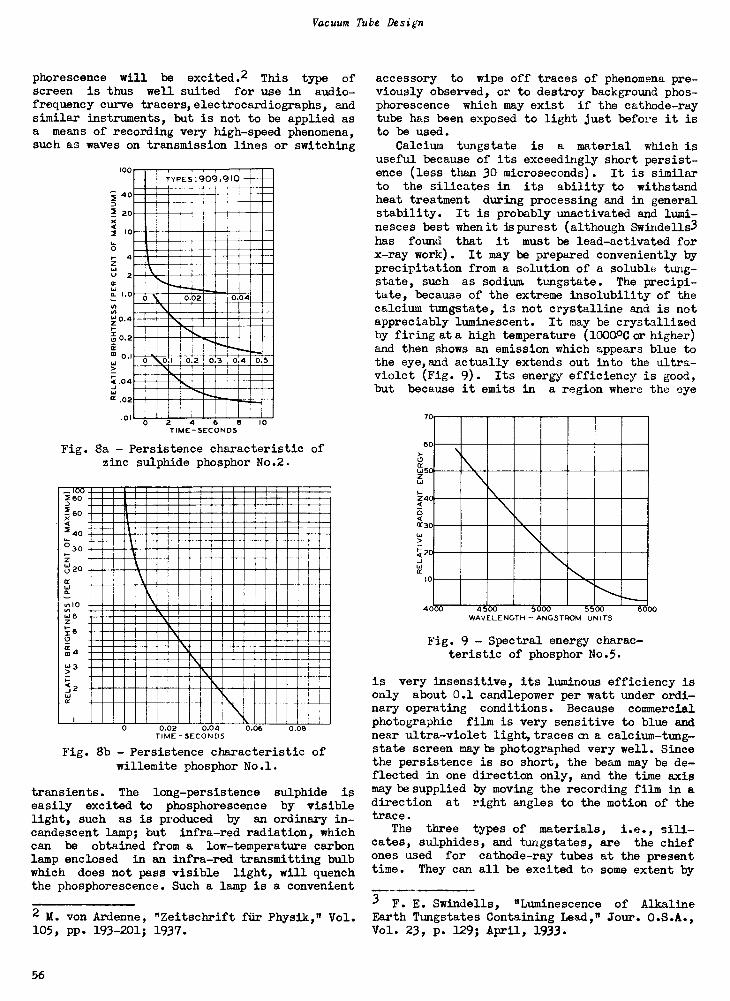
Vacuum Tube Design
phorescence will be excited.2 This type ofscreen is thus well suited for use in audio -
frequency curve tracers, electrocardiographs, andsimilar instruments, but is not to be applied asa means of recording very high-speed phenomena,such as waves on transmission lines or switching
100
3 40
20
2 10
04
2
a. 1.0
001110.4
0.2
m 0.1
ti .04
cl .02
.01
ryPEs:909,910
0 0..02 0.04
0 0I 02 03 04 05
0 2 4TIME-SECONDS
10
Fig. 8a - Persistence characteristic ofzinc sulphide phosphor No.2.
-100280
604m40,030ZU 20
wm
v,10w8Z1-16LIFc
m4L.1>
ti ,J .W
1
0 0.02 0.04 0.06TIME-SECONDS
0.08
Fig. 8b - Persistence characteristic ofwillemite phosphor No.l.
transients. The long -persistence sulphide iseasily excited to phosphorescence by visiblelight, such as is produced by an ordinary in-candescent lamp; but infra -red radiation, whichcan be obtained from a low -temperature carbonlamp enclosed in an infra -red transmitting bulbwhich does not pass visible light, will quenchthe phosphorescence. Such a lamp is a convenient
2 M. von Ardenne, "Zeitschrift fur Physik," Vol.105, pp. 193-201; 1937.
accessory to wipe off traces of phenomena pre-viously observed, or to destroy background phos-phorescence which may exist if the cathode-raytube has been exposed to light just before it isto be used.
Calcium tungstate is a material which isuseful because of its exceedingly short persist-ence (less than 30 microseconds). It is similarto the silicates in its ability to withstandheat treatment during processing and in generalstability. It is probably unactivated and lumi-nesces best when it is purest (although Swindells3has found that it must be lead -activated forx-ray work). It may be prepared conveniently byprecipitation from a solution of a soluble tung-state, such as sodium tungstate. The precipi-tate, because of the extreme insolubility of thecalcium tungstate, is not crystalline and is notappreciably luminescent. It may be crystallizedby firing at a high temperature (100(10C or higher)
and then shows an emission which appears blue tothe eye, and actually extends out into the ultra-violet (Fig. 9). Its energy efficiency is good,but because it emits in a region where the eye
70
60
0
Z4
0Cr 30
<2_1
10
4000 4600 5000 5500 6WAVELENGTH - ANGSTROM UNITS
000
Fig. 9 - Spectral energy charac-teristic of phosphor No.5.
is very insensitive, its luminous efficiency isonly about 0.1 candlepower per watt under ordi-nary operating conditions. Because commercialphotographic film is very sensitive to blue andnear ultra -violet light,tracescn a calcium-tung-state screen may be photographed very well. Sincethe persistence is so short, the beam may be de-flected in one direction only, and the time axismay be supplied by moving the recording film in adirection at right angles to the motion of thetrace.
The three types of materials, i.e., sili-cates, sulphides, and tungstates, are the chiefones used for cathode-ray tubes at the presenttime. They can all be excited to some extent by
3 F. E. Swindells, "Luminescence of AlkalineEarth Tungstates Containing Lead," Jour. O.S.A.,Vol. 23, p. 129; April, 1933.
56
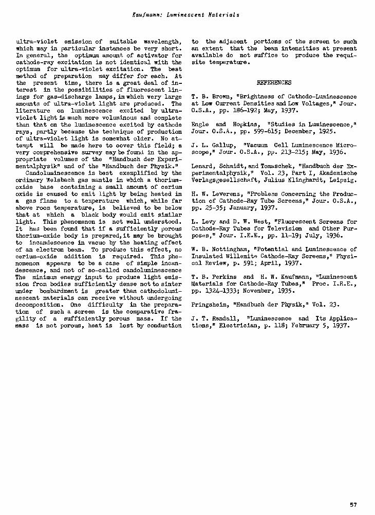
Kaufmann: Luminescent Materials
ultra -violet emission of suitable wavelength,which may in particular instances be very short.In general, the optimum amount of activator forcathode-ray excitation is not identical with theoptimum for ultra -violet excitation. The bestmethod of preparation may differ for each. Atthe present time, there is a great deal of in-terest in the possibilities of fluorescent lin-ings for gas -discharge lamps, in which very largeamounts of ultra -violet light are produced. Theliterature on luminescence excited by ultra-violet light is much more voluminous and completethan that on the luminescence excited by cathoderays, partly because the technique of productionof ultra -violet light is somewhat older. No at-tempt will be made here to cover this field; avery comprehensive survey may be found in the ap-propriate volumes of the "Handbuch der Experi-mentalphysik" and of the "Handbuch der Physik."
Candoluminescence is best exemplified by theordinary Welsbach gas mantle in which a thorium -oxide base containing a small amount of ceriumoxide is caused to emit light by being heated ina gas flame to a temperature which, while farabove room temperature, is believed to be belowthat at which a black body would emit similarlight. This phenomenon is not well understood.It has been found that if a sufficiently porousthorium -oxide body is prepared, it may be broughtto incandescence in vacuo by the heating effectof an electron beam. To produce this effect, nocerium -oxide addition is required. This phe-nomenon appears to be a case of simple incan-descence, and not of so-called candoluminescenceThe minimum energy input to produce light emis-sion from bodies sufficiently dense not to sinterunder bombardment is greater than cathodolumi-nescent materials can receive without undergoingdecomposition. One difficulty in the prepara-tion of such a screen is the comparative fra-gility of a sufficiently porous mass. If themass is not porous, heat is lost by conduction
to the adjacent portions of the screen to suchan extent that the beam intensities at presentavailable do not suffice to produce the requi-site temperature.
REFERENCES
T. B. Brown, "Brightness of Cathodo -Luminescenceat Low Current Densities and Low Voltages," Jour.O.S.A., pp. 186-192; May, 1937.
Engle and Hopkins, "Studies in Luminescence,"Jour. O.S.A., pp. 599-615; December, 1925.
J. L. Gallup, "Vacuum Cell Luminescence Micro-scope," Jour. O.S.A., pp. 213-215; May, 1936.
Lenard, Schmidt, and Tomaschek, "Handbuch der Ex-perimentalphysik," Vol. 23, Part I, AkademischeVerlagsgesellschaft, Julius Klinghardt, Leipzig.
H. W. Leverenz, "Problems Concerning the Produc-tion of Cathode -Ray Tube Screens," Jour. O.S.A.,pp. 25-35; January, 1937.
L. Levy and D. W. West, "Fluorescent Screens forCathode -Ray Tubes for Television and Other Pur-poses," Jour. I.E.E., pp. 11-19; July, 1936.
W. B. Nottingham, "Potential and Luminescence ofInsulated Willemite Cathode -Ray Screens," Physi-cal Review, p. 591; April, 1937.
T. B. Perkins and H. W. Kaufmann, "LuminescentMaterials for Cathode -Ray Tubes," Proc. I.R.E.,pp. 1324-1333; November, 1935.
Pringsheim, "Handbuch der Physik," Vol. 23.
J. T. Randall, "Luminescence and Its Applica-tions," Electrician, p. 118; February 5, 1937.
57
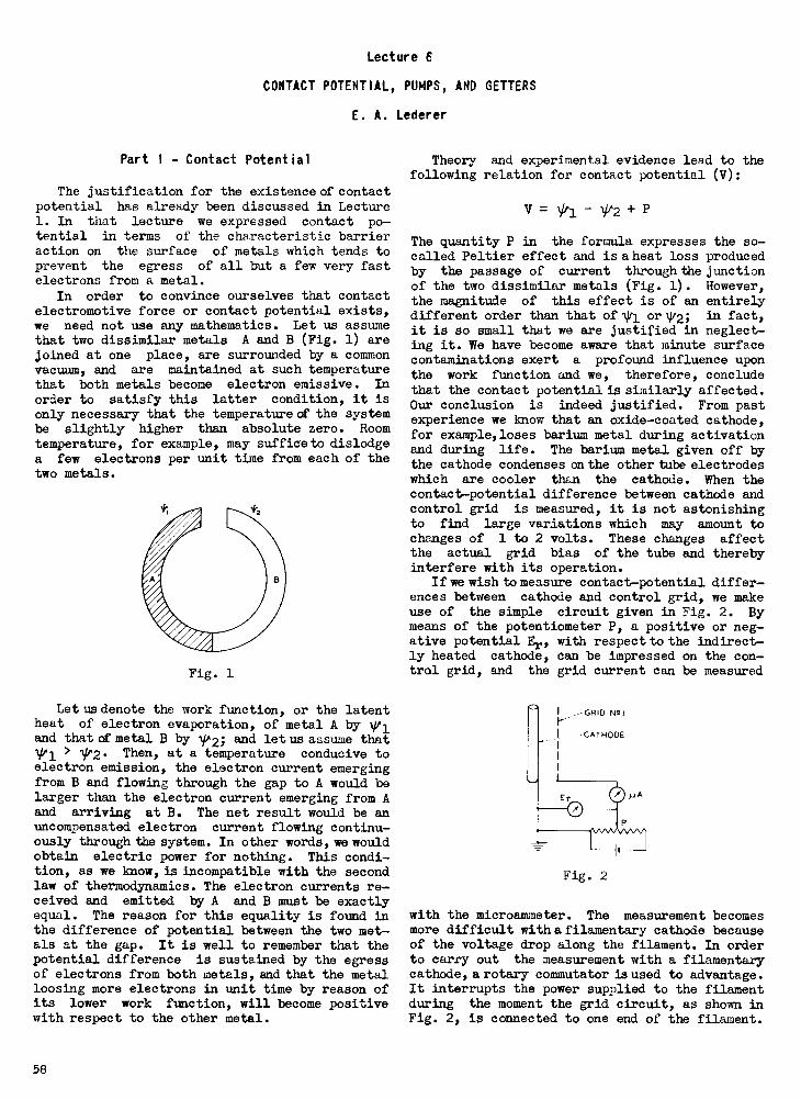
Lecture 6
CONTACT POTENTIAL, PUMPS, AND GETTERS
E. A. Lederer
Part I - Contact Potential
The justification for the existence of contactpotential has already been discussed in Lecture1. In that lecture we expressed contact po-tential in terms of the characteristic barrieraction on the surface of metals which tends toprevent the egress of all but a few very fastelectrons from a metal.
In order to convince ourselves that contactelectromotive force or contact potential exists,we need not use any mathematics. Let us assumethat two dissimilar metals A and B (Fig. 1) arejoined at one place, are surrounded by a commonvacuum, and are maintained at such temperaturethat both metals become electron emissive. In
order to satisfy this latter condition, it isonly necessary that the temperaturece the systembe slightly higher than absolute zero. Roomtemperature, for example, may suffice to dislodgea few electrons per unit time from each of thetwo metals.
Fig. 1
Let us denote the work function, or the latentheat of electron evaporation, of metal A by V'land that cf metal B by 1p2; and let us assume thatVa. > V2. Then, at a temperature conducive toelectron emission, the electron current emergingfrom B and flowing through the gap to A would belarger than the electron current emerging from Aand arriving at B. The net result would be anuncompensated electron current flowing continu-ously through the system. In other words, we wouldobtain electric power for nothing. This condi-tion, as we know, is incompatible with the secondlaw of thermodynamics. The electron currents re-ceived and emitted by A and B must be exactlyequal. The reason for this equality is found inthe difference of potential between the two met-als at the gap. It is well to remember that thepotential difference is sustained by the egressof electrons from both metals, and that the metalloosing more electrons in unit time by reason ofits lower work function, will become positivewith respect to the other metal.
Theory and experimental evidence lead to thefollowing relation for contact potential (V):
V = 1/11 - V/2 + P
The quantity P in the formula expresses the so-called Peltier effect and is aheat loss producedby the passage of current through the junctionof the two dissimilar metals (Fig. 1). However,the magnitude of this effect is of an entirelydifferent order than that of *1 orlif2; in fact,it is so small that we are justified in neglect-ing it. We have become aware that minute surfacecontaminations exert a profound influence uponthe work function and we, therefore, concludethat the contact potential is similarly affected.Our conclusion is indeed justified. From pastexperience we know that an oxide -coated cathode,for example,loses barium metal during activationand during life. The barium metal given off bythe cathode condenses on the other tube electrodeswhich are cooler than the cathode. When thecontact -potential difference between cathode andcontrol grid is measured, it is not astonishingto find large variations which may amount tochanges of 1 to 2 volts. These changes affectthe actual grid bias of the tube and therebyinterfere with its operation.
If we wish to measure contact -potential differ-ences between cathode and control grid, we makeuse of the simple circuit given in Fig. 2. Bymeans of the potentiometer P, a positive or neg-ative potential Er, with respect to the indirect-ly heated cathode, can be impressed on the con-trol grid, and the grid current can be measured
Fig. 2
with the microammeter. The measurement becomesmore difficult with a filamentary cathode becauseof the voltage drop along the filament. In orderto carry out the measurement with a filamentarycathode, a rotary commutator is used to advantage.It interrupts the power supplied to the filamentduring the moment the grid circuit, as shown inFig. 2, is connected to one end of the filament.
58
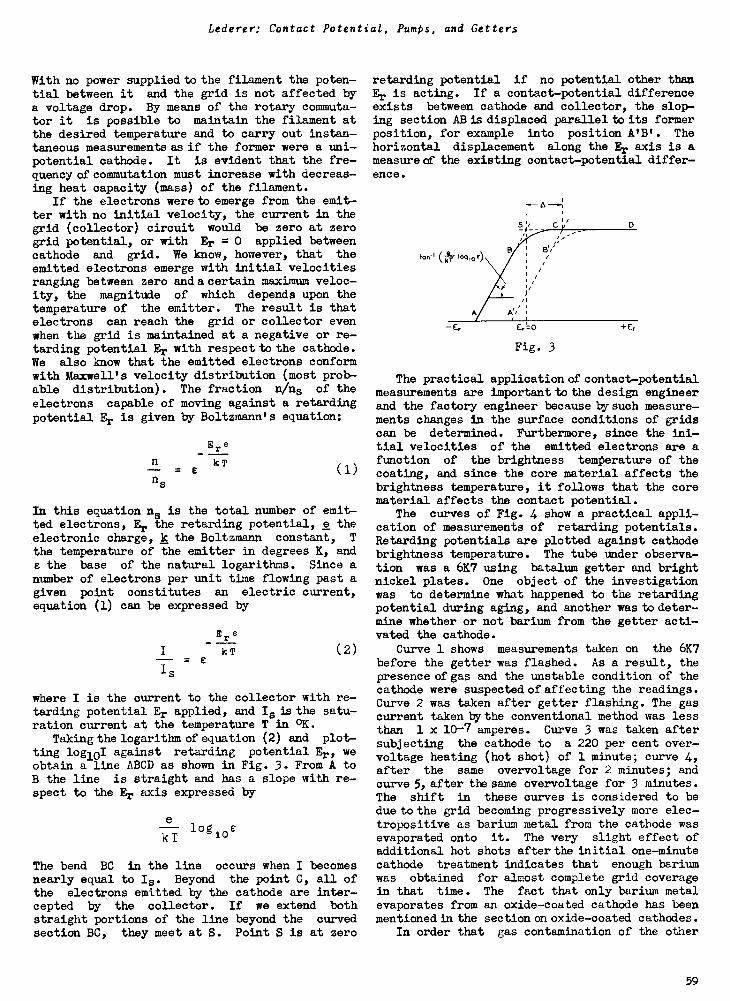
Lederer: Contact Potential, Pumps, and Getters
With no power supplied to the filament the poten-tial between it and the grid is not affected bya voltage drop. By means of the rotary commuta-tor it is possible to maintain the filament atthe desired temperature and to carry out instan-taneous measurements as if the former were a uni-potential cathode. It is evident that the fre-quency of commutation must increase with decreas-ing heat capacity (mass) of the filament.
If the electrons were to emerge from the emit-ter with no initial velocity, the current in thegrid (collector) circuit would be zero at zerogrid potential, or with Er = 0 applied betweencathode and grid. We know, however, that the
emitted electrons emerge with initial velocitiesranging between zero ands certain maximum veloc-ity, the magnitude of which depends upon thetemperature of the emitter. The result is thatelectrons can reach the grid or collector evenwhen the grid is maintained at a negative or re-tarding potential Er with respect to the cathode.We also know that the emitted electrons conformwith Maxwell's velocity distribution (most prob-able distribution). The fraction nins of the
electrons capable of moving against a retardingpotential Er is given by Boltzmann's equation:
ErekT
= e
ns( 1 )
In this equation ns is the total number of emit-ted electrons, Er the retarding potential, e theelectronic charge, k the Boltzmann constant, T
the temperature of the emitter in degrees K, ande the base of the natural logarithms. Since anumber of electrons per unit time flowing past agiven point constitutes an electric current,equation (1) can be expressed by
EreI kT- = E
Is
( 2 )
where I is the current to the collector with re-tarding potential Er applied, and Is is the satu-ration current at the temperature T in °K.
Taking the logarithm of equation (2) and plot-ting logioI against retarding potential Er, weobtain a line ABCD as shown in Fig. 3. From A toB the line is straight and has a slope with re-spect to the Er axis expressed by
e- g EkT 10
The bend BC in the line occurs when I becomesnearly equal to Is. Beyond the point C, all ofthe electrons emitted by the cathode are inter-cepted by the collector. If we extend bothstraight portions of the line beyond the curvedsection BC, they meet at S. Point S is at zero
retarding potential if no potential other thanEr is acting. If a contact -potential differenceexists between cathode and collector, the slop-ing section AB is displaced parallel to its formerposition, for example into position A'B'. Thehorizontal displacement along the Er axis is ameasurecf the existing contact -potential differ-ence.
loqie)
5 C
A
0
-Er Er O
Fig. 3
+ Er
The practical application of contact -potentialmeasurements are important to the design engineerand the factory engineer because by such measure-ments changes in the surface conditions of gridscan be determined. Furthermore, since the ini-tial velocities of the emitted electrons are afunction of the brightness temperature of thecoating, and since the core material affects thebrightness temperature, it follows that the corematerial affects the contact potential.
The curves of Fig. 4 show a practical appli-cation of measurements of retarding potentials.Retarding potentials are plotted against cathodebrightness temperature. The tube under observa-tion was a 6K7 using batalum getter and brightnickel plates. One object of the investigationwas to determine what happened to the retardingpotential during aging, and another was to deter
whether or not barium from the getter acti-vated the cathode.
Curve 1 shows measurements taken on the 6K7before the getter was flashed. As a result, thepresence of gas and the unstable condition of thecathode were suspected of affecting the readings.Curve 2 was taken after getter flashing. The gascurrent taken by the conventional method was lessthan 1 x 10⁻⁷ amperes. Curve 3 was taken aftersubjecting the cathode to a 220 per cent over -voltage heating (hot shot) of 1 minute; curve 4,after the same overvoltage for 2 minutes; andcurve 5, after the same overvoltage for 3 minutes.The shift in these curves is considered to bedue to the grid becoming progressively more elec-tropositive as barium metal from the cathode wasevaporated onto it. The very slight effect ofadditional hot shots after the initial one -minutecathode treatment indicates that enough bariumwas obtained for almost complete grid coveragein that time. The fact that only barium metalevaporates from an oxide -coated cathode has beenmentioned in the section on oxide -coated cathodes.
In order that gas contamination of the other
59

Vacuum Tube Design
electrodes might be studied, gas was released inthe 6K7 by the following procedure. The cathodewas maintained at 11000K, grid No.1 was allowedto float, and a positive potential sufficient togive a cathode current of 40 milliamperes for 3minutes was applied to the other electrodes. Afterthis treatment, curve 6 was taken. It indicatesthat barium metal was removed from grid No.1 bychemical combination with the gas previouslyliberated.
From this description and the curves of Fig. 4,we can make the following deductions: (1) no ba-
1.6
1.2
tn
O
-1 0.4
17.
z
0 0a.
0zCt -0.4
CC
0.8
0.
CURVE DESCRIPTION
-N2 INe 2No 3
INITIALX AFTER GETTER FLASH0 AFTER I -MINUTE HOT SHOTA AFTER 2 -MINUTE HOT SHOT0 AFTER 3 -MINUTE HOT SHOT13 AFTER BOMBARDMENT
Not
N24N55N26
N22
....... ,...
N26
N223 34
N5
1
a
-.......0
800 850 900 950 1000 1050CATHODE TEMPERATURE -DEGREES K
Fig. 4
rium metal from the getter reaches the cathodeor the No.1 grid; (2) a hot shot of one minutefurnishes enough barium metal from the cathodeto coat grid No.1 at least with a monatomic lay-er; (3) successive additional hot shots merelyproduce more barium metal which may even out barespots in the already existing barium layer ongrid No.1; and (4) considerable gas is producedwhen heating or bombarding the electrodes, otherthan grid No.l. Although the nature of the gas isnot known, we do know that it combines with bariummetal and very probably is CO and H2.
The investigation of retarding potentials wascontinued by making measurements on a 6K7-0 takenfrom stock. This tube had been aged previous tothe measurements. The results of these measure-ments are shown in Fig. 5. It will be noted thatall curves are practically straight and the slopeappears almost constant. At first, the constancyof the slope and the straightness of the lineswere surprising. However, the explanation ofthese facts rests again on equation (2), i.e.,the relation between initial velocities and cath-ode temperature. After changing to common loga-rithms and substituting numerical values forBoltzmann's constant, the electronic charge, and
changing from e.s.u. to volts, we can rewriteequation (2) as
log - = - 5050 --- (2a)is
In the equation, i is the collector or grid cur-rent (see Fig. 2) at the retarding potential Er,and is is the saturation current which the cath-ode is capable of delivering at temperature T°K.
From measurements taken on a 6K7 tube, usingan oxide -coated cathode with an emitting area of0.718 sq cm, and determining Er for i fixed ar-bitrarily at 5.0 x 10⁻⁷ amperes, we obtain thedata in Table I.
Table I
T*
°K
is
amperes
i
amperes
Er
volts.-s
1°g10 -i;nEr/100°C
1000 48.8 5.0 x 10⁻⁷ 1.780 1.024 x 10⁻⁸ 2.010 - 10-0.367
900 4.31 " 1.413 1.16 x 10⁷ 3.065 - 10-0.347
800 0.269 n 1.066 1.86 x 10⁻⁶ 4.270 - 10-0.352
700 7.18 x 10⁻³ " 0.714 6.96 x 10⁻⁵ 5.843 - 10-0.368
600 39.5 x 10⁻⁶ n 0.346 1.265 x 10⁻² 8.102 - 10
* Cathode temperature was measured in the middle Average = -0.359of the cathode, i.e., at its hottest part.(Brightness temperature is used in both the calculated and measured val-ues of the slope of the lines.)
60
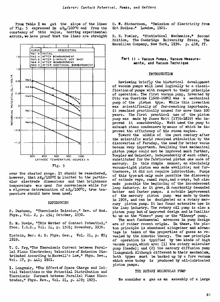
Lederer: Contact Potential, Pumps, and Getters
From Table I we get the slope of the linesof Fig. 5 expressed in aEr/100°C and from theconstancy of this value, barring experimentalerrors, we have proof that the lines are straight
1.6
1.2
In
-10 0.8
Lal
4 0.4
1.=
z
0.
0zaa-0.4ct
0
-0.8
-1.2
I I I I I I
CURVE DESCRIPTIONN2 1 0Ns 2 0
INITIALAFTER BOMBARDMENT
N23 6N54 N55 X
AFTER 3 -MINUTEAFTER BOMBARDMENTAFTER ADDITIONAL
HOT SHOT
BOMBARDMENT
N95
Na 4
N81
N53
800 850 900 950 1000CATHODE TEMPERATURE -DEGREES K
Fig. 5
over the charted range. It should be remembered,however, that aEr/1000C is limited to the partic-ular electrode dimensions and that brightnesstemperature was used for convenience while fora rigorous determination of aEr/100°C, true tem-perature should have been used.
REFERENCES
S. Dushman, "Thermionic Emission," Rev. of Mod.Phys., Vol. 2, p. 454; October, 1930.
R. M. Bowie, "This Matter of Contact Potential,"Proc. I.R.E., Vol. 24, p. 1501; November, 1936.
Epstein, Ber. d. D. Phys. Ges., Vol. 21, p. 85;
1919.
T. C. Fry,"The Thermionic Current between Paral-lel Plane Electrodes; Velocities of Emission Dis-tributed According to Maxwell's Law," Phys. Rev.,Vol. 17, p. 441; 1921.
I. Langmuir, "The Effect e£ Space Charge and Ini-tial Velocities on the Potential Distribution andThermionic Current between Parallel Plane Elec-trodes," Phys. Rev., Vol. 21, P. 419; 1923.
O. W. Richardson, "Emission of Electricity fromHot Bodies." London, 1921.
R. H. Fowler, "Statistical Mechanics," SecondEdition, The Cambridge University Press, TheMacmillan Company, New York, 1936. p. 418, ff.
Part II - Vacuum Pumps, Vacuum Measure-ments, and Vacuum Technique
INTRODUCTION
Reviewing briefly the historical developmentof vacuum pumps will lead logically to a classi-fication of pumps with respect to their principleof operation. The first vacuum pump, invented byOtto von Guericke (1602-1686) was a mechanicalpump of the piston type. While this inventionwas scientifically of far-reaching importance,it remained practically unused for more than 100years. The first practical use of the pistonpump was made by James Watt (1736-1819) who im-proved it considerably. Watt used the pump toexhaust steam condensers by means of which he im-proved the efficiency of his steam engine.
Toward the middle of the past century afterthe scientific world received stimulation by thediscoveries of Faraday, the need for better vacuabecame very important. Realizing that mechanicalpiston pumps could not be improved much further,Toepleremd Geissler, independently of each other,substituted for the fabricated piston one made ofmercury. In this simple manner, an absolutelyvacuum -tight piston was made available; and fur-thermore, it did not require lubrication. Pumpsof this type not only made possible the discoveryof cathode rays, canal rays, and x-rays, but alsomade possible the beginning of the incandescentlamp industry. As it grew, it constantly demandedbetter and faster pumps. A notable improvementof the mercury piston pump was made by Gaedein 1905, and can be designated as a rotary mer-cury piston pump. It has found extensive use inthe lamp industry. The rotary oil pump is also apiston pump but of improved design and is familiarto us as the "Cenco" pump or the "Kinney" pump.
The most fundamental advances in pump designare of rather recent origin. In these, the pis-ton principle is abandoned altogether and advan-tage is taken of the properties of gases as re-vealed by the kinetic theory. The new principleof operation is typified by two kinds of highvacuum pumps,which are: (1) the rotary molecularpump (Gaede); and (2) the mercury diffusion pump(Langmuir). Although different in their mechanism,both types must be backed up by a fore vacuumwhich even today is produced by oil -lubricatedpiston pumps.
THE ROTARY MOLECULAR PUMP
We consider a gas as an assembly of a large
61
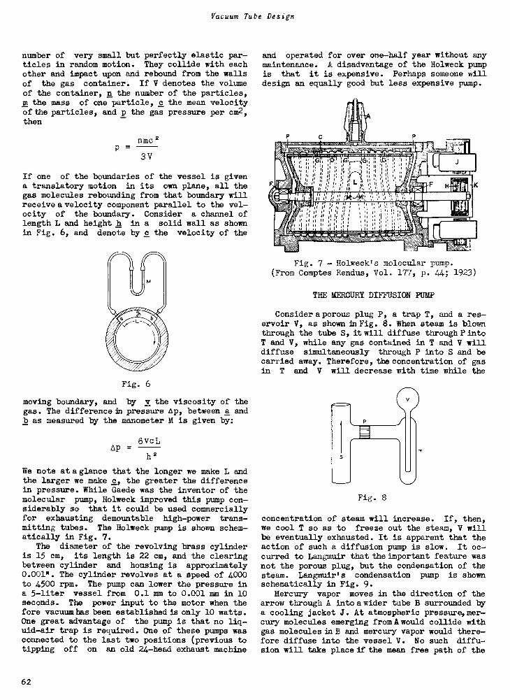
Vacuum Tube Design
number of very small but perfectly elastic par-ticles in random motion. They collide with eachother and impact upon and rebound from the wallsof the gas container. If V denotes the volumeof the container, n the number of the particles,m the mass of one particle, c the mean velocityof the particles, and p the gas pressure per cm2,then
mac 2
P =3V
If one of the boundaries of the vessel is givena translatory motion in its own plane, all thegas molecules rebounding from that boundary willreceive a velocity component parallel to the vel-ocity of the boundary. Consider a channel oflength L and height h in a solid wall as shownin Fig. 6, and denote by c the velocity of the
Fig. 6
moving boundary, and by v the viscosity of thegas. The difference in pressure Ap, between a andb as measured by the manometer M is given by:
6 v c L
813 =h2
We note at a glance that the longer we make L andthe larger we make c, the greater the differencein pressure. While Gaede was the inventor of themolecular pump, Holweck improved this pump con-siderably so that it could be used commerciallyfor exhausting demountable high-power trans-mitting tubes. The Holweck pump is shown schem-atically in Fig. 7.
The diameter of the revolving brass cylinderis 15 cm, its length is 22 cm, and the clearingbetween cylinder and housing is approximately0.001". The cylinder revolves at a speed of 4000to 4500 rpm. The pump can lower the pressure ina 5-liter vessel from 0.1 mm to 0.001 mm in 10seconds. The power input to the motor when thefore vacuum has been established is only 10 watts.One great advantage of the pump is that no liq-uid-air trap is required. One of these pumps wasconnected to the last two positions (previous totipping off on an old 24-head exhaust machine
and operated for over one-half year without anymaintenance. A disadvantage of the Holweck pumpis that it is expensive. Perhaps someone willdesign an equally good but less expensive pump.
Is
,ukklpeprIPTmgImpr,mr.morgma
\Av:'77,1/47AW"---1AC-;%Z
Fig. 7 - Holweck's molecular pump.(From Comptes Rendus, Vol. 177, p. 44; 1923)
THE MERCURY DIFFUSION PUMP
Consider aporous plug P, a trap T, and a res-ervoir V, as shown in Fig. 8. When steam is blownthrough the tube S, it will diffuse through PintoT and V, while any gas contained in T and V willdiffuse simultaneously through P into S and becarried away. Therefore, the concentration of gasin T and V will decrease with time while the
Fig. 8
concentration of steam will increase. If, then,we cool T so as to freeze out the steam, V willbe eventually exhausted. It is apparent that theaction of such a diffusion pump is slow. It oc-curred to Langmuir that the important feature wasnot the porous plug, but the condensation of thesteam. Langmuir's condensation pump is shownschematically in Fig. 9.
Mercury vapor moves in the direction of thearrow through A into a wider tube B surrounded bya cooling jacket J. At atmospheric pressure,mer-cury molecules emerging from A would collide withgas molecules in B and mercury vapor would there-fore diffuse into the vessel V. No such diffu-sion will take place if the mean free path of the
62
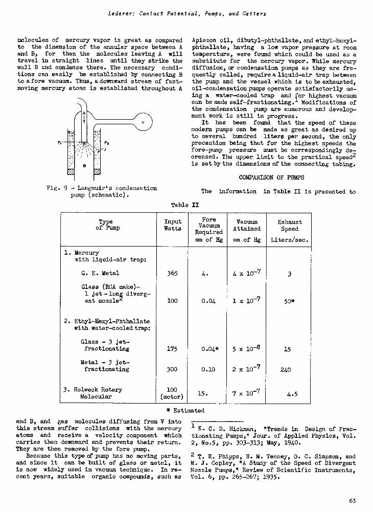
Lederer: Contact Potential, Pumps, and Getters
molecules of mercury vapor is great as comparedto the dimension of the annular space between Aand B, for then the molecules leaving A willtravel in straight lines until they strike thewall B and condense there. The necessary condi-tions can easily be established by connecting Bto afore vacuum. Thus, a downward stream of fast-moving mercury atoms is established throughout A
Pu
Fig. 9 - Langmuir's condensationpump (schematic).
Apiezon oil, dibutyl-phthallate, and ethyl -hexyl-phthallate, having a low vapor pressure at roomtemperature, were found which could be used as asubstitute for the mercury vapor. While mercurydiffusion, or condensation pumps as they are fre-quently called, require a liquid -air trap betweenthe pump and the vessel which is to be exhausted,oil -condensationpumps operate satisfactorily us-ing a water-cooled trap and for highest vacuumcan bemadeself-fractionating.1 Modifications ofthe condensation pump are numerous and develop-ment work is still in progress.
It has been found that the speed of thesemodern pumps can be made as great as desired upto several hundred liters per second, the onlyprecaution being that for the highest speeds thefore -pump pressure must be correspondingly de-creased. The upper limit to the practical speed2is set by the dimensions of the connecting tubing.
Table II
COMPARISON OF PUMPS
The information in Table II is presented to
Typeof Pump
InputWatts
ForeVacuumRequiredmm of Hg
VacuumAttained
mm of Hg
ExhaustSpeed
Liters/sec.
1. Mercurywith liquid -air trap:
G. E. Metal 365 4. 4 x 10⁻⁷ 3
Glass (RCA make) -1 jet -long diverg-ent nozzle' 100 0.04 1 x 10⁻⁷ 50*
2. Ethyl -Hexyl -Phthallatewith water-cooled trap:
Glass - 3 jet -fractionating 175 0.04* 5 x 10-8 15
Metal - 3 jet -fractionating 300 0.10 2 x 10⁻⁷ 240
3. Holweck Rotary 100Molecular (motor)
15. 7 x 10⁻⁷ 4.5
* Estimated
and B, and gas molecules diffusing from V intothis stream suffer collisions with the mercuryatoms and receive a velocity component whichcarries them downward and prevents their return.They are then removed by the fore pump.
Because this type of pump has no moving parts,and since it can be built of glass or metal, itis now widely used in vacuum technique. In re-cent years, suitable organic compounds, such as
1K. C. D. Hickman, "Trends in Design of Frac-
tionating Pumps," Jour. of Applied Physics, Vol.2, No.5, pp. 303-313; May, 1940.
2 T. E. Phipps, H. M. Tenney, O. C. Simpson, andM. J. Copley, "A Study of the Speed of DivergentNozzle Pumps," Review of Scientific Instruments,Vol. 6, pp. 265-267; 1935.
63
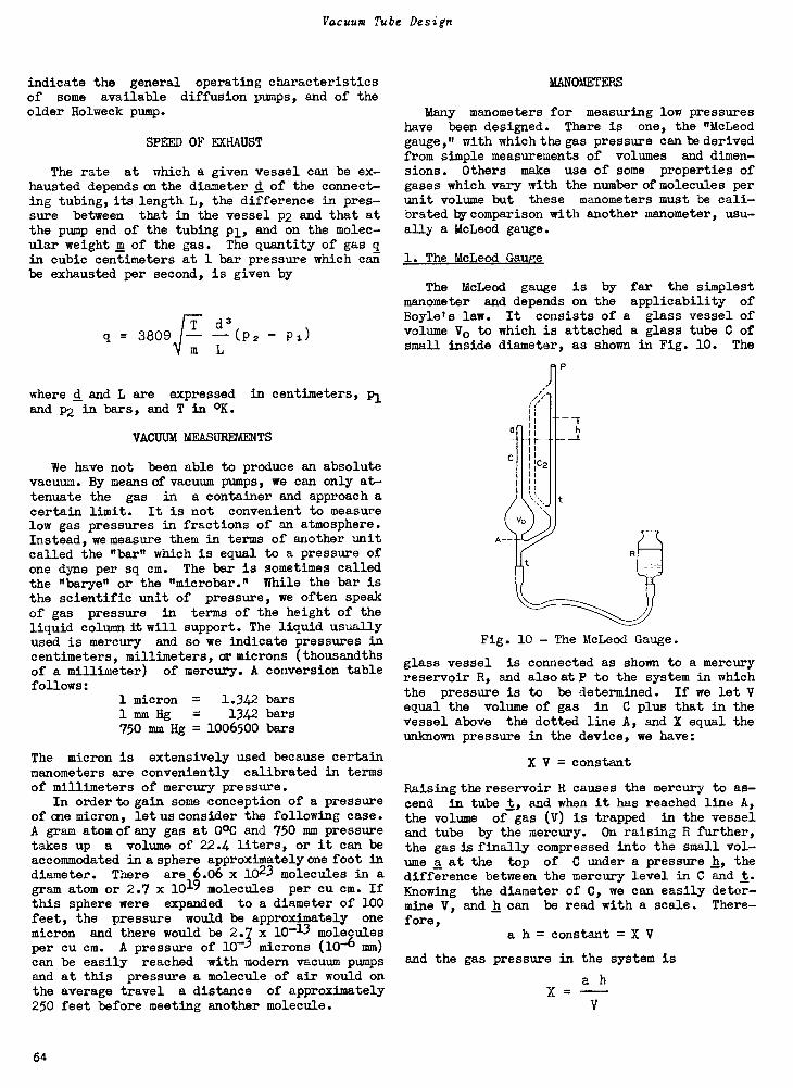
Vacuum Tube Design
indicate the general operating characteristicsof some available diffusion pumps, and of theolder Holweck pump.
SPEED OF EXHAUST
The rate at which a given vessel can be ex-hausted depends on the diameter d of the connect-ing tubing, its length L, the difference in pres-sure between that in the vessel p2 and that atthe pump end of the tubing pl, and on the molec-ular weight m of the gas. The quantity of gas qin cubic centimeters at 1 bar pressure which canbe exhausted per second, is given by
q = 3809T c13,- 2 - Pi)
where d and L are expressed in centimeters, piand P2 in bars, and T in °K.
VACUUM MEASUREMENTS
We have not been able to produce an absolutevacuum. By means of vacuum pumps, we can only at-tenuate the gas in a container and approach acertain limit. It is not convenient to measurelow gas pressures in fractions of an atmosphere.Instead, we measure them in terms of another unitcalled the "bar" which is equal to a pressure ofone dyne per sq cm. The bar is sometimes calledthe "barye" or the "microbar." While the bar isthe scientific unit of pressure, we often speak
of gas pressure in terms of the height of theliquid column it will support. The liquid usuallyused is mercury and so we indicate pressures incentimeters, millimeters, or microns (thousandthsof a millimeter) of mercury. A conversion tablefollows:
1 micron = 1.342 bars1 mm Hg = 1342 bars750 mm Hg = 1006500 bars
The micron is extensively used because certainmanometers are conveniently calibrated in termsof millimeters of mercury pressure.
In order to gain some conception of a pressureof one micron, let us consider the following case.A gram atom of any gas at 00C and 750 mm pressuretakes up a volume of 22.4 liters, or it can beaccommodated in a sphere approximately one foot in
diameter. There are 6.06 x 10²³ molecules in agram atom or 2.7 x 10¹⁹ molecules per cu cm. Ifthis sphere were expanded to a diameter of 100feet, the pressure would be approximately one
micron and there would be 2.7 x 10⁻¹³ moleculesper cu cm. A pressure of 10-, microns (10-6 mm)can be easily reached with modern vacuum pumpsand at this pressure a molecule of air would onthe average travel a distance of approximately250 feet before meeting another molecule.
MANOMETERS
Many manometers for measuring low pressureshave been designed. There is one, the "McLeodgauge," with which the gas pressure can be derivedfrom simple measurements of volumes and dimen-sions. Others make use of some properties ofgases which vary with the number of molecules perunit volume but these manometers must be cali-brated by comparison with another manometer, usu-ally a McLeod gauge.
1. The McLeod Gauge
The McLeod gauge is by far the simplestmanometer and depends on the applicability of
Boyle's law. It consists of a glass vessel ofvolume Vo to which is attached a glass tube C ofsmall inside diameter, as shown in Fig. 10. The
Fig. 10 - The McLeod Gauge.
glass vessel is connected as shown to a mercuryreservoir R, and also at P to the system in whichthe pressure is to be determined. If we let Vequal the volume of gas in C plus that in thevessel above the dotted line A, and X equal theunknown pressure in the device, we have:
X V = constant
Raising the reservoir R causes the mercury to as-
cend in tube t, and when it has reached line A,the volume of gas (V) is trapped in the vesseland tube by the mercury. On raising R further,the gas is finally compressed into the small vol-ume a at the top of C under a pressure h, thedifference between the mercury level in C and t.Knowing the diameter of C, we can easily deter-mine V, and h can be read with a scale. There-fore,
a h = constant = X V
and the gas pressure in the system is
a hX -
V
64
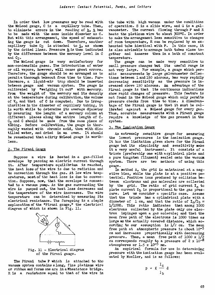
Lederer: Contact Potential, Pumps, and Getters
In order that low pressures may be read withthe McLeod gauge, C is a capillary tube. Then,to eliminate errors in the reading of h, t hasto be made with the same inside diameter as C.But with this arrangement, the speed of exhaust-ing the gauge is cut down. Therefore, anothercapillary tube C2 is attached to t, as shownby the dotted lines. Pressure his then indicatedby the difference between the mercury level in Cand C2.
The McLeod gauge is very satisfactory fornon -condensible gases. The introduction of wateror oil vapors, however, will cause great errors.Therefore, the gauge should be so arranged as topermits thorough bakeout from time to time. Fur-thermore, a liquid -air trap should be insertedbetween gauge and vacuum system. The gauge iscalibrated by "weighing it out" with mercury.From the weight of the mercury and its densityat the temperature during calibration, the volumeof Vo and that of C is computed. Due to irreg-ularities in the diameter of capillary tubing, itis worth while to determine its average diameterby measuring the length of a mercury column atdifferent places along the entire length of C.C2 and C should be made from the same piece oftubing. Before calibration, the gauge is thor-oughly washed with chromic acid, then with dis-tilled water, and dried in an oven. It shouldbe remembered that a dirty McLeod gauge is worth-
less.
2. The Pirani Gauge
Suppose a wire is heated in a gas -filled
envelope by passing an electric current throughit. After temperature equilibrium is reached,the heat loss of the wire is due to radiation andto convection through the gas. At low wire temp-eratures, most of the heat loss is due to convec-tion. Suppose, now, that the envelope is connec-ted to a vacuum pump. As the gas surrounding thewire is pumped out, the heat loss decreases andthe temperature of the wire increases. The wiretemperature can be determined by measuring itselectrical resistance. The foregoing is a simpleexplanation of the "Pirani gauge," the electricaldiagram of which is shown in Fig. 11.
Fig. 11 - Electrical diagramof the Pirani gauge.
The Pirani tube P which is attached to thevacuum system contains a long, fine platinum wireor ribbon and forms one arm in alTheatstone bridge.R is a resistance equal to that of the wire in
the tube with high vacuum under the conditionsof operation. S is a slide wire, and G is a gal-vanometer. The current flowing through P and Rheats the platinum wire to about 3000C. In orderto make the arrangement less sensitive to changesof room temperature, R can be replaced by an ex-hausted tube identical with P. In this case, itis also advisable to arrange both tubes close to-gether and immerse them in a bath of constanttemperature.
The gauge can be made very sensitive tosmall pressure changes but its useful range isnot very large. For example, a gauge which per-mits measurements by large galvanometer deflec-tions between 1 and 150 microns, has very rapidlydecreasing sensitivity as the pressure is in-creased above 150 microns. An advantage of thePirani gauge is that its continuous indicationsshow rapid changes of pressure. This feature isnot found in the McLeod gauge which only permitspressure checks from time to time. A disadvan-tage of the Pirani gauge is that it must be cal-ibrated against a McLeod gauge for every gas.Thus, accurate measurements with a Pirani gaugerequire a knowledge of the gas present in thesystem.
3. The Ionization Gauze
An extremely sensitive gauge for measuringthe lowest pressures is the ionization gauge.It has the limitation given above for the Piranigauge but its simplicity and sensitivity makeit a very useful instrument. It consists of atriode (preferably one with acylindral plate anda pure tungsten filament) sealed onto the vacuumsystem. There are two methods of using thisgauge.
In method A, the grid is maintained at a neg-ative bias, while the plate is at a positive po-tential. Positive ions produced by collision be-tween electrons and gas molecules are collectedby the grid. The ratio of grid current Ic toplate current Ib is proportional to the gas pres-sure. Let us consider a specific case. Assumethat the triode has a cylindrical plate with adiameter of 1 cm, and that the ratio of Io/Ib =1/1000. This ratio indicates that among 1000electrons collected by the plate only one elec-tron impinges upon a gas molecule; and that themean free path of the electrons is 1000 times aslarge as the actually covered distance, which ac-cording to our assumption is 1/2 cm. The meanfree path at atmospheric pressure is about 10-5cm and increases proportionally with decreasingpressure. Thus, a mean free path of 1000 x 1/2cm corresponds roughly to a pressure of 2 x 10⁻⁸atmospheres or 1.5 x 10⁻⁵ mm.
An empirical formula for use in determiningpressure with the ionization gauge has been eval-uated by Moeller, and is as follows:
Icp = K - d
Ib
65
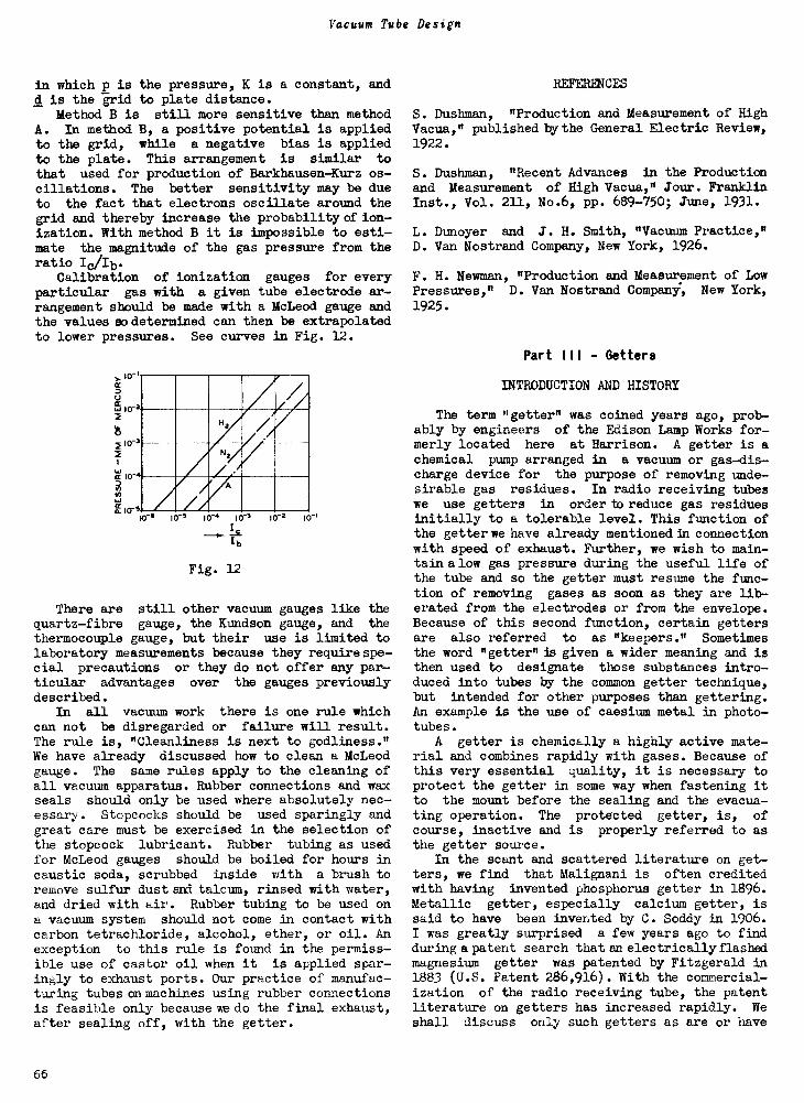
Vacuum Tube Design
in which p is the pressure, K is a constant, andd is the grid to plate distance.
Method B is still more sensitive than methodA. In method B, a positive potential is appliedto the grid, while a negative bias is appliedto the plate. This arrangement is similar to
that used for production of Barkhausen-Kurz os-cillations. The better sensitivity may be dueto the fact that electrons oscillate around thegrid and thereby increase the probability of ion-ization. With method B it is impossible to esti-mate the magnitude of the gas pressure from theratio IdIb.
Calibration of ionization gauges for everyparticular gas with a given tube electrode ar-rangement should be made with a McLeod gauge andthe values so determined can then be extrapolatedto lower pressures. See curves in Fig. 12.
10-1CC
UCC
W 10-2
010-3
2
a to -4
H2
to -4
N2/
to -3
12
m-2 to -
There are still other vacuum gauges like thequartz -fibre gauge, the Kundson gauge, and the
thermocouple gauge, but their use is limited tolaboratory measurements because they require spe
precautions or they do not offer any par-ticular advantages over the gauges previouslydescribed.
In all vacuum work there is one rule whichcan not be disregarded or failure will result.The rule is, "Cleanliness is next to godliness."We have already discussed how to clean a McLeodgauge. The same rules apply to the cleaning ofall vacuum apparatus. Rubber connections and waxseals should only be used where absolutely nec-essary. Stopcocks should be used sparingly andgreat care must be exercised in the selection ofthe stopcock lubricant. Rubber tubing as usedfor McLeod gauges should be boiled for hours incaustic soda, scrubbed inside with a brush toremove sulfur dust and talcum, rinsed with water,and dried with air. Rubber tubing to be used ona vacuum system should not come in contact withcarbon tetrachloride, alcohol, ether, or oil. Anexception to this rule is found in the permiss-ible use of castor oil when it is applied spar-ingly to exhaust ports. Our practice of manufac-turing tubes on machines using rubber connectionsis feasible only because we do the final exhaust,after sealing off, with the getter.
REFERENCES
S. Dushman, "Production and Measurement of HighVacua," published by the General Electric Review,1922.
S. Dushman, "Recent Advances in the Productionand Measurement of High Vacua," Jour. FranklinInst., Vol. 211, No.6, pp. 689-750; June, 1931.
L. Dunoyer and J. H. Smith, "Vacuum Practice,"D. Van Nostrand Company, New York, 1926.
F. H. Newman, "Production and Measurement of LowPressures," D. Van Nostrand Company, New York,
1925.
Part III - Getters
INTRODUCTION AND HISTORY
The term "getter" was coined years ago, prob-ably by engineers of the Edison Lamp Works for-merly located here at Harrison. A getter is achemical pump arranged in a vacuum or gas -dis-charge device for the purpose of removing unde-sirable gas residues. In radio receiving tubeswe use getters in order to reduce gas residuesinitially to a tolerable level. This function ofthe getter we have already mentioned in connectionwith speed of exhaust. Further, we wish to main-tain a low gas pressure during the useful life ofthe tube and so the getter must resume the func-tion of removing gases as soon as they are lib-erated from the electrodes or from the envelope.Because of this second function, certain gettersare also referred to as "keepers." Sometimesthe word "getter" is given a wider meaning and isthen used to designate those substances intro-duced into tubes by the common getter technique,but intended for other purposes than gettering.An example is the use of caesium metal in photo -tubes.
A getter is chemically a highly active mate-rial and combines rapidly with gases. Because ofthis very essential quality, it is necessary toprotect the getter in some way when fastening itto the mount before the sealing and the evacua-ting operation. The protected getter, is, ofcourse, inactive and is properly referred to asthe getter source.
In the scant and scattered literature on get-ters, we find that Malignani is often creditedwith having invented phosphorus getter in 1896.Metallic getter, especially calcium getter, issaid to have been invented by C. Soddy in 1906.I was greatly surprised a few years ago to findduring a patent search that an electrically flashedmagnesium getter was patented by Fitzgerald in1883 (U.S. Patent 286,916). With the commercial-ization of the radio receiving tube, the patentliterature on getters has increased rapidly. Weshall discuss only such getters as are or have
66
Lederer: Contact Potential, Pumfrs, and Getters
been used for factory production.Chemically active materials which in one form
or another are used as getters are given in thefollowing list.
PhosphorusMagnesium
CalciumStrontiumBarium
LithiumSodiumPotassiumRubidiumCaesium
Alkaline earthmetals
Alkali metals
Cerium, Lanthanum*
The properties of each of these materials willbe discussed later on.
ACTION OF CLEAN-UP
If we vaporize or disperse a getter materialin an imperfect vacuum, the probability of combi-nation between the vapor and the residual gas isvery great. Hence, the clean-up action is veryfast. In describing this action we refer to (a)gettering by dispersion during which the vaporizedgetter combines rapidly with the residual gas andthe surplus of the vapor settles on the coolersections of the bulb or electrodes; (b) contactgettering during which the getter deposits com-bine slowly with residual gas which comes in con-tact with them due to temperature agitation; and(c) clean-up by ionization during which a rapidchemical reaction takes place between a getterdeposit and an ionized gas. These three phasesof gas clean-up are generally observed with anygetter.
SHIELDING
Getter deposits are often undesired on tubeelectrodes and particularly on the insulating mem-bers of the tube structure. In order to keep thegetter from depositing where it is not wanted,shields are used. Shielding is only effective ifthe mean free path of the getter vapor is largeas compared with the distance between origin ofvapor and location of deposit. When this is thecase, the getter vapor travels in straight lines.Fortunately, this condition ordinarily exists inall tubes we are dealing with. There is also onefurther point which should be remembered in con-nection with dispersed gettering. Even if thepressure in the device is too high at first tosatisfy the straight-line requirement, the pres-sure will fall rapidly after traces of the getter
are vaporized.
PHOSPHORUS
Phosphorus occurs in several modifications,two of which, the yellow and the red, are of in-terest to us. Yellow phosphorus melts at 44°Cand ignites in air when heated to 50°C. If yellowphosphorus is finely divided (such as it is onfilter paper dipped in asolution of yellow phos-phorus in carbonbisulfide), it ignites even atroom temperature. Yellow phosphorus is very poi-sonous.
Heating yellow phosphorus in a closed container(under pressure) for several days at 260°C givesthe red phosphorus. Red phosphorus ignites in airabove 400°C and is chemically much less activethan the yellow modification. When red phosphorusis heated in vacuum, it reverts again to the morevolatile yellow modification. These propertiesof phosphorus make it very convenient for use asgetter, chiefly to remove traces of oxygen.
The lamp industry uses a suspension of redphosphorus into which the tungsten filaments aredipped. A trace of red phosphorus remains on thewire. It is chemically inactive in air duringmounting of the filament, and even during sealing -in. After the lamp is exhausted and the filamentis heated for the first time, it is reconvertedto the yellow modification and is then capable ofremoving oxygen contained in the residual gas.
The same technique was used with the earlytypes of radio receiving and transmitting tubesemploying pure tungsten filaments. Since an ex-cess of phosphorus did not interfere with theoperation of the tube, a liberal supply of it waspainted on the plate from which it was liberatedby high -frequency heating of the plate or by in-ternal bombardment of the plate. As mentioned inconnection with the properties of the thoriatedfilament, red phosphorus was also used in connec-tion with magnesium getter in the types 199 and201-A. Both of these types used a fine thoriated-tungsten filament. The beneficial action ofphosphorus consisted of cleaning up the layer ofnickel oxide on the plates. As a result, the"poisoning effect" of the nickel oxide on the fil-ament was eliminated.
Phosphorus getter cannot be used in tubes withoxide -coated filaments for it would combine imme-diately with the free barium in the coating. Likeoxygen, phosphorus poisons the emission of oxide
cathodes. Back in 1931, a 24 -head exhaustmachine on which 201 -A's with phosphorus and mag-nesium getter were made caused considerableshrinkage when it was used for exhausting type227. It was found necessary to change the portrubbers and sweeps, and to clean the manifoldthoroughly to remove all traces of phosphorusvapor.
MAGNESIUM
Magnesium metal is chemically very active. It* and some other rare earth metals (many of which reduces water vapor slowly at as lowa temperatureconstitute misch metal) as 100°C and it has a considerable vapor pressure
67
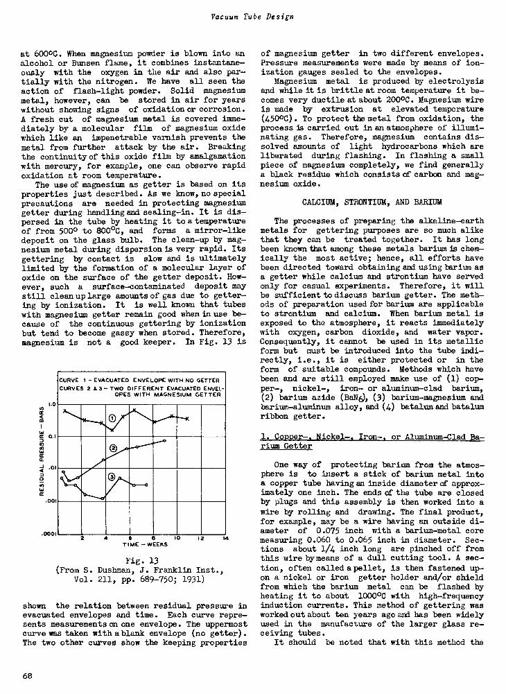
Vacuum Tube Design
at 6000C. When magnesium powder is blown into analcohol or Bunsen flame, it combines instantane-ously with the oxygen in the air and also par-tially with the nitrogen. We have all seen theaction of flash -light powder. Solid magnesiummetal, however, can be stored in air for yearswithout showing signs of oxidation or corrosion.
A fresh cut of magnesium metal is covered imme-diately by a molecular film of magnesium oxidewhich like an impenetrable varnish prevents the
metal from further attack by the air. Breakingthe continuity of this oxide film by amalgamationwith mercury, for example, one can observe rapidoxidation at room temperature.
The use of magnesium as getter is based on itsproperties just described. As we know, no specialprecautions are needed in protecting magnesiumgetter during handling and sealing -in. It is dis-persed in the tube by heating it to a temperatureof from 500° to 800°C, and forms a mirror-likedeposit on the glass bulb. The clean-up by mag-nesium metal during dispersion is very rapid. Itsgettering by contact is slow and is ultimatelylimited by the formation of a molecular layer ofoxide on the surface of the getter deposit. How-ever, such a surface -contaminated deposit maystill cleanuplarge amounts of gas due to getter-ing by ionization. It is well known that tubeswith magnesium getter remain good when in use be-cause of the continuous gettering by ionizationbut tend to become gassy when stored. Therefore,magnesium is not a good keeper. In Fig. 13 is
1.0
0001
CURVE 1 - EVACUATED ENVELOPE WITH NO GETTERCURVES 2 & 3- TWO DIFFERENT EVACUATED ENVEL-
OPES WITH MAGNESIUM GETTER
2 4 6 6 10TIME - WEEKS
12
Fig. 13(From S. Dushman, J. Franklin Inst.,
Vol. 211, pp. 689-750; 1931)
14
shown the relation between residual pressure inevacuated envelopes and time. Each curve repre-sents measurements on one envelope. The uppermostcurve was taken with a blank envelope (no getter).The two other curves show the keeping properties
of magnesium getter in two different envelopes.Pressure measurements were made by means of ion-ization gauges sealed to the envelopes.
Magnesium metal is produced by electrolysisand while it is brittle at room temperature it be-comes very ductile at about 20000. Magnesium wireis made by extrusion at elevated temperature(450°C). To protect the metal from oxidation, theprocess is carried out in an atmosphere of illumi-nating gas. Therefore, magnesium contains dis-solved amounts of light hydrocarbons which areliberated during flashing. In flashing a smallpiece of magnesium completely, we find generallya black residue which consists of carbon and mag-nesium oxide.
CALCIUM, STRONTIUM, AND BARIUM
The processes of preparing the alkAline-earthmetals for gettering purposes are so much alikethat they can be treated together. It has longbeen known that among these metals barium is chem-ically the most active; hence, all efforts havebeen directed toward obtaining and using bariun asa getter while calcium and strontium have servedonly for casual experiments. Therefore, it willbe sufficient to discuss barium getter. The meth-ods of preparation used for barium are applicableto strontium and calcium. When barium metal isexposed to the atmosphere, it reacts immediatelywith oxygen, carbon dioxide, and water vapor.Consequently, it cannot be used in its metallicform but must be introduced into the tube indi-rectly, i.e., it is either protected or in theform of suitable compounds. Methods which havebeen and are still employed make use of (1) cop-per-, nickel-, iron- or aluminum -clad barium,(2) barium azide (BaNO, (3) barium -magnesium andbarium -aluminum alloy, and (4) batalum and batalumribbon getter.
1. Copper-. Nickel-. Iron-. or Aluminum -Clad Ba-rium Getter
One way of protecting barium from the atmos-phere is to insert a stick of barium metal intoa copper tube having an inside diameter of approx-imately one inch. The ends of the tube are closedby plugs and this assembly is then worked into awire by rolling and drawing. The final product,for example, may be a wire having an outside di-ameter of 0.075 inch with a barium -metal coremeasuring 0.060 to 0.065 inch in diameter. Sec-tions about 1/4 inch long are pinched off fromthis wire by means of a dull cutting tool. A sec-tion, often called a pellet, is then fastened up-on a nickel or iron getter holder and/or shieldfrom which the barium metal can be flashed byheating it to about 1000°C with high -frequencyinduction currents. This method of gettering wasworked out about ten years ago and has been widelyused in the manufacture of the larger glass re-ceiving tubes.
It should be noted that with this method the
68
Lederer: Contact Potential, Pumps, and Getters
pinched ends of the pellets do not have an air-tight seal. Therefore, corrosion of the bariummetal can take place, and once started, it pro-gresses inward rapidly. Consequently, the getteraction is satisfactory only with fresh pellets orthose on which corroded ends have been cut off.As an aid in evacuation, degassing of the getterprevious to flashing is essential. Changing theprotective sheathfrom copper to nickel, aluminum,or iron has little influence upon the generalqualities of the pellet.
The flashing occurs when enough pressure isbuilt up inside the pellet to eject amixture con-taining barium vapor as well as molten barium, andsometimes molten copper or aluminum, depending onwhichever material is used for the sheath. Par-ticles of the molten material often stick to theglass and cause microscopic surface cracks whichwiden in three or four weeks to form air leaks.
The barium deposit produced by this methodgenerally has a dark color indicating that thepresence of much gas during flashing reacted withthe barium to form an impure deposit. Pure ba-rium -metal deposits are almost indistinguishablein appearance from a magnesium deposit.
Recently, iron -clad barium wire has been pro-posed for metal tubes. In this form the wire hasan outside diameter of 0.015 to 0.020 inch. Thethickness of the iron sheath is from 0.002 to0.0025 inch. A section of such wire is heated bypassing current through it. The use of iron as aprotective casing permits spot-welding the sec-tion between two lead wires. In order to facili-tate the escape of barium -metal vapor and at thesame time to produce adirectional flash, the cas-ing is ground flat, as shown in Fig. 14. The ba-rium vapor breaks through the iron casing where
THICKNESS«.001"
.01o"
.015°
Fig. 14
the wall thickness is a minimum. Besides, theflat surface of the getter wire is intended to actas a shield confining most of the getter depositto the section of the bulb near the flat surfaceand limited roughly by a plane coincident with it.
2. Barium-Azide Getter (BaN6)
In Lecture 2 on oxide -coated cathodes, a brief
discussion of the barium -vapor process, carriedout with barium-azide as the barium source, wasgiven. Much more barium metal was used with thisprocess than was needed for filament activation,and so the surplus served as getter. Later, ba-rium azide was used in Europe as a barium sourcefor tubes using ordinary oxide -coated filaments.The getter source was made as follows: A nickel -mesh disk 3/4 inch in diameter with a centeredhole 1/4 inchin diameter, was dipped into a con-centrated solution of BaN6 in water, and thenallowed to dry. When this prepared disk (oftendesignated by the name "life-saver") was heatedin the tube during bakeout, nitrogen was liber-ated at about 1500C. The remaining barium metalwas flashed from the life -saverbyapplying high -frequency heating. The life-saver shape was cho-sen because it heats up uniformly in a high -fre-quency field. A round disk made from material ofpoor heat conductivity (such as mesh) without acenter hole heats at the edge first while thecenter is relatively cold. No efforts were madeto produce a directional effect except that pro-vided by the plate which shadowed the tube struc-ture and the mica spacers.
Examining this getter critically, we find thatthe decomposition of BaN6 is not complete butthat the barium metal formed combines with partof the nitrogen. The result is that the surfaceof the life-saver has a mixture of barium nitrideand barium metal. Consequently, when high -fre-quency heating is applied to the disk, the flashis accompanied by a second evolution of nitrogengas. As a rule, the getter deposits appear dark,indicating vaporization in the presence of gas.
Fabricating the getter is objectionable owingto the danger of handling barium azide. The dryazide is very explosive and traces dropped on thefloor may cause fire if they are stepped on. Thesaturated azide solution (17% maximum at roomtemperature), is not dangerous except that it ishighly poisonous like all soluble barium com-pounds when taken internally. BaN6 can be readilyoxidized with potassium permanganate (KMn04), andso the work of dipping the nickel -mesh disks inthe azide solution is carried out over a lead -lined sink which is flushed from time to timewith KMn04 solution.
Reimann has studied the activity of barium -metal deposits in cleaning up gases. As a resultof experimental evidence, he contends that a blackbarium -metal deposit cleans up gases by contactgettering about 4 to 5 times as fast as a brightmetallic -barium mirror. The reason was sought inthe difference of actual to apparent surface whichno doubt is greater with the black deposit. Mr.Wamsley and I have observed exactly opposite ef-fects. While this question should be definitelysettled by further experiments, it is of no greatpractical consequence because contact getteringtakes place only during shelf life, and as longas the gas pressure does not increase, the qualityof the tube remains unaffected.
It is well known that contact gettering in
69
Vacuum Tube Design
tubes using pure magnesium getter is so poor thatthe gas pressure increases on standing. Thisdrawback has been overcome completely by the useof barium getter which permits the maintenance ofa vacuum of the order of 10-7 mm for as long atime as free barium metal is available.
3. Barium -Magnesium and Barium -Aluminum AlloyGetter
In order to protect barium metal from attackby the atmosphere, attempts have been made toalloy it with other metals. When the alloy is
heated in vacuum, barium metal is vaporized toserve as the clean-up agent. Barium -magnesium al-loy has gained wide usage. If the barium contentof this alloy does not exceed 25 per cent byweight, the alloy is stable in dry air and can bestored for long periods. However, owing to thedifference of vapor pressure of the two constitu-ent metals, large amounts of magnesium are vapor-ized during flashing before dispersion of thebarium takes place. For example, if we use apiece of alloy weighing 5 milligrams, about 3 to 4milligrams of magnesium must be evaporated beforeany but traces of barium are dispersed. Thisquantity of magnesium is very large fora medium-sized glass tube. Fortunately, with the magnesiumassuming the role of cleaning up the bulk of thegas, only very small amounts of free barium arerequired to serve as a"keeper" during shelf life.A serious disadvantage in the use of barium -mag-nesium getter is that one cannot tell by visualinspection of the flash whether or not any- of thebarium metal has been dispersed.
No such limitation exists with barium -aluminumgetter. This alloy contains from 45 to 50 percent barium metal by weight. When this alloygetter is flashed, barium evaporates first; and ifnickel or iron tabs (or getter holders) are used,no aluminum is dispersed. The amount of bariumflash can, therefore, be judged by inspection. Itis obvious that an alloy should contain as largea percentage of barium as is comparable with goodstability in air. This maximum barium ratio isattained at about 50 per cent. Such an alloy de-composes slowly at 70 per cent relative humidityat 80°F.
Barium -aluminum alloy in reality isa chemicalcompound because during its preparation the heatof the melt increases exothermically from about700° to 1700°C. Consequently, energy has to beexpended to liberate barium metal during theflashing operation. Hence,barium-aluminum getterrequires a high flashing temperature. Fortunate-ly, this temperature is not so high as to preventus from using nickel or iron tabs, although caremust be exercised not to melt the tabs. It issometimes advantageous to use a small amount ofmagnesium as precleaning agent with the barium -aluminum alloy. The magnesium may be mechanicallyadmixed to the barium -aluminum alloy, or mixturesof barium -magnesium and barium -aluminum alloys maybe used. Such mixtures were employed at the be-
ginning of metal -tube manufacture. Although heat-ing of the getter was carried out at the maximumpermissible shell temperature, chemical analysisrevealed that practically no barium (only magne-sium metal) was flashed.
Barium -magnesium as well as barium -aluminumalloys, with barium ratio as given above, arebrittle at room temperature. It is customary,therefore, to pulverize the alloys and compact the
powder into small pellets on a pill -press. Ac-cording to usage, the weight of getter pelletsvaries from 2 1/2 to 30 milligrams. ,When suchpellets are flashed, variable amounts of gas areliberated. The amounts vary within such wide
limits that a special study of these conditionshas been started.
Another factor affecting the temperature offlashing is the thermal contact between tab andpellet. Latest developments take this factor intoconsideration. Hence, more uniform results areobtained with so-called imbedded getters, i.e.,pellets pressed into the getter tab.
Both types of alloy getters are widely used inthe manufacture of glass tubes and undoubtedly theresults are better than if magnesium getters wereused. However, there is still room for improve-ment. A barium getter for glass tubes requiringa low flashing temperature and permitting visualinspection of the amount of barium deposit mayimprove quality and decrease shrinkage consider-ably.
4. Batalum and Batalum-Ribbon Getter
Batalum getter has been devised for use inmetal tubes. It is areaction-type getter and de-rives alkaline -earth metal from its oxide whichis reduced at elevated temperature with tantalummetal. Since we desired to produce barium withtantalum, the name "batalum" was coined to indi-cate this combination. The reaction is expressed
by the formula:
5 Be° + 2 Ta -* Ta205 + 5 Ba
Owing to its volatility, the barium metal is re-moved from the sphere of reaction and, therefore,it proceeds in the direction of the arrow. How-ever, Ta205 (tantalum pentoxide) reacts with ba-rium oxide forming barium tantalate,according tothe formula
3 Ba0 + Ta205 Ba3Ta208
Therefore, the complete process can be representedby
8 Ba0 + 2 Ta 5 Ba + Ba3Ta208
Accurate measurements of the barium yield and theoriginal amount of barium compound (weighed ascarbonate) indicate the general correctness ofthis formula. The temperature required for thereaction is about 13000 - 1500°C. The process ismost conveniently carried out by coating a tanta-
70
Lederer: Contact Potential, Pumps, and Getters
lum wire with barium and strontium carbonates,converting the carbonates to the oxides at about10000 - 1100°C, and then raising the temperatureto about 1300°C at which barium and strontiummetal evaporates. Barium and strontium carbonateswere used, because, as we know, barium carbonatealone melts and would cause sputtering. The re-ducing agent, the tantalum, in form of a wire hastwo main advantages. First, it affords controlover the reaction by limiting the reaction surfaceto that of the wire. Thus, in controlling thewire temperature, we can start and stop the evap-oration of barium at will. The second advantageis of chemical nature, and results from combiningthe wire (which serves as a heater) and reducingagent into one and the same unit.
In its first form the batalum getter consistedofatantalum coil sprayed with the double carbo-nates (presintered in air to increase their densi-ty) and provided with a shield for directing theflash.3 Flashing of the getter was accomplishedby heating the tantalum wire electrically. Whilethe results obtained with this getter were satis-factory, it has two disadvantages. One was itscost and the other was a processing requirement.The carbonate coating required decomposition
during exhaust. Both disadvantages were elimi-nated by the so-called "ribbon getter." Thisgetter consisted of a tantalum strip 1.5 x 0.1 x0.0025 cm, with the middle section formed into achannel approximately 1 cm long. The barium com-pound, mixed with a nitrocellulose binder wasfilled into the channel on an automatic machinewhich formed and cut the channel and dried thecoating. Since the channel which was coated onlyon the concave side was in itself a shield, andsince the preparation of the getter was carriedout entirely on amachine, the cost of the getterwas only a small fraction of that of the coilgetter.
The disadvantage of decomposing the carbonatesduring exhaust has been overcome by using barium-berylliate as coating material for the ribbongetter. This is a compound formed from the basicbarium oxide with the amphoteric beryllium oxideand is approximately represented by the formulaBaBe02.
Because of its advantages, the ribbon getterhas found wide application in metal tubes. Bothtypes of batalum getters (made in our own factoryunder controlled conditions to insure quality andpurity) yield alkaline -earth metal of very highpurity. The getters may be flashed partially orcompletely on the exhaust machine, and the flashis controlled completely by the temperature ofthe tantalum carrier. For most purposes it isadvantageous to flash the getter after sealingoff, i.e., before or during aging of the tube.
3 E. A. Lederer and D. R. Wamsley, "'Batalum,' ABarium Getter for Metal Tubes," RCA Review, Vol.2, pp. 117-123; July, 1937.
THE GROUP OF ALKALI METALS
The alkali metals, lithium, sodium, potassium,rubidium, and caesium are chemically very activebut cannot be used for radio receiving -tube get-ters because of their high vapor pressure. Theiruse is confined to special devices, such ascaesium -vapor detector tubes, phototubes, vaporlamps, and gas -discharge devices. In the latter,they serve as a means for reducing the "cathodefall." An alkali metal is introduced into thedevice either as a metal by vacuum distillationor is produced by reduction. While it is rela-tively easy to produce an alkali metal by reactionwith a suitable reducing agent (vacuum decomposi-tion of the tartarates, iron, aluminum, or calciumwith the halides, oxides, carbonates, etc.), it isadvantageous to use alkali compounds free fromwater of crystallization and such reactions as donot produce gas. For example, caesium metal isconveniently produced by heating an intimate mix-ture of caesium dichromate or permanganate withsilicon or boron. The formulas are:
Cs2Cr207 + 2 Si = Cr203 + 2 Si02 + 2 Cs
2 CsMn04 + 2 Si = 2 Mn02 + 2 Si02 + 2 Cs
Both reactions are exothermic and once started ata temperature of about 900°C proceed until thereducing agent is used up. Therefore, the con-trol is poor and reflashing of the getter isobviously useless. Notwithstanding these facts,reactions using purified silicon are extensivelyused in the manufacture of phototubes and Icono-scopes. Rubidium and potassium can be made in asimilar manner. Lithium and sodium can be pro-duced by reacting the respective berylliates withtantalum, titanium, or aluminum.
MISCH METAL
Misch metal is a mixture of the rare-earthmetals and contains much cerium and lanthanum andin addition variable amounts of sodium but notover 5 per cent. This material has been proposedoften as getter for various devices. There is nodoubt that the heat of combustion of both ceriumand lanthanum is very high and that misch metalmay be an excellent material for dispersion get-tering to remove traces of air. Misch metal forcontact gettering is obviously very inferior tobarium, because the former can be stored in dryair for many weeks while the latter reacts rapidlywith the oxygen in the air. It is believed thatmisch metal is covered by a molecular layer ofoxide which protects the metal from rapid oxida-tion. Misch metal is now used in gas -filled vol-tage regulators (type 874) as an oxygen getterand as a means to maintain the uniformity and mag-nitude of the cathode fall during life.
71

Vacuum Tube Design
REFERENCES
S. Dushman, "Recent Advances in the Productionand Measurement of High Vacua," Jour. FranklinInst., Vol. 211, No.6, pp. 689-750; June, 1931.
Andrews and Bacon, "TheCommercial Getters," J.
53, p. 1674; 1931.
A. D. Power, "GetteringReferences a, Part III.
A. L. Reiman, "Clean-up of Gases by Magnesium," A. D. Power, "GetteringPhil. Mag., Vol. 16, pp. 673-86; 1933. References b, Part III.
Comparison of CertainAmer. Chem. Soc., Vol.
of Hydrogen," Ref. 6-
of Nitrogen," Ref. 6-
72

Lecture 7
METALLURGICAL PRINCIPLES
S. Umbreit
INTRODUCTION
"Careful research into the nature of themetallic state has yet to discover, with anycertainty, its essential quality. We do not yetknow, for sure, what it is that makes the me-tallic elements different from, if not actuallyunique among created things. We do know, of
course, that metals have certain more or lesscharacteristic properties -they are hard, strong,and tough, and good conductors of heat and elec-tricity, and these so-called metallic propertiesprovide a definition of a sort. However, it isthe structure rather than the behavior of themetals which gives the really fundamental in-formation necessary to the understanding of metal -
licity"As everyone knows, metals owe their in-
dustrial importance to the fact that they pos-sess, often in a peculiar sense, useful proper-ties, such as strength, plasticity, electricalconductivity, and ferromagnetism. These andother properties find their origin in the internalstructure of the metal or alloy. What a metaldoes is because of what it is. Metallic behavioris simply an outward manifestation of what is,and what goes on, unseen, inside The basicfact underlying nearly all metallic behavior isthat a metal is crystalline in its nature; anymass of metal that has been formed in the ordi-nary way is made up of many small crystals tightlybound together."*
These words of L. R. VanWert,1 of Harvard,state the subject very well.
NUCLEI AND GRAIN GROWTH
If a piece of metal is polished, appropri-ately etched, and examined under a microscope,it is at once apparent that the mass is granularin character but not in the sense that eachgrain visible under the microscope has a defi-nite shape and proportion as do mineralogicalspecimens. The irregular polyhedral shape ofthe metallic crystallite is due to the fact thatit grew rapidly in a liquid of high concentra-tion, whereas the mineral grew at an exceedinglyslow rate from a dilute concentration. However,both crystals do have the common feature thatthe atoms are arranged with great regularity bothas to position and spacing.
This regularity distinguishes the crystal-line solid from the liquid and from glasses in
1 L. R. VanWert, "Inside a Metal," Mining and
Metallurgy; October, 1937.
* Quotation with permission of Mining and Metal-lurgy.
which the atoms are arranged with random orien-tation and spacing. This appearance of the crys-talline material in a liquid is called freezingwhich occurs in a pure metal at a single fixedtemperature and coincides, in most cases, withthe temperature at which the crystalline phasedisappears on heating.
During the cooling of a melt of metal, crys-tallization centers or nuclei are formed spon-taneously at the surface of the container. Fromthese nuclei, the crystals grow in all direc-tions but more rapidly in certain directions thanin others. These crystals grow together so thatthe boundary planes form irregular polyhedra dueto the mutual interference of one another. Thefreezing of a melt is not a simple affair butdepends upon two factors which determine whetherthe melt will freeze on cooling or whether itwill become a glass, and if it crystallizes,whether the grains will be coarse or fine. Thesetwo factors are: the number of nuclei and the rateof grain growth. Both factors must be large atthe same temperature to produce a granular solid.The number of nuclei and the rate of grain growthare generally large in the case of metals butnot so in the case of the alkaline silicateswhich constitute our glasses. In the latter case,the appearance of nuclei does not occur untilthe liquid has cooled to a point where the vis-cosity is high and the rate of grain growth hasdiminished to zero. Consequently, the mass re-mains glassy.
The difference between the behavior of a
molten mass of a crystalline substance and thatof a vitreous or glassy substance upon cooling,is that the former reaches a temperature wherethe crystalline, solid phase appears and furthercooling results in a completely solid mass.Heating causes the disappearance of the crystal-lites at the same temperature. In other words,there is an abrupt change in viscosity or ri-gidity when the freezing or melting temperatureis passed.
With a vitreous substance like glass or
pitch, there is no abrupt increase in viscosityon cooling but rather a gradual increase extend-ing down to or below room temperature. The mass
gradually changes from a liquid to a solid andit is hard to say when it is a liquid and when asolid.
The behavior of a pure metal and glass is
illustrated in Fig. 1, which shows the rate of
grain growth (GG) and number of nuclei (NN)
plotted against decreasing temperature. In me-
tals the number of nuclei present is large at
a temperature where the rate of grain growth islarge; consequent1y,crystallization occurs. How-ever, in glass the number of nuclei present inthe temperature range of appreciable grain growth
73
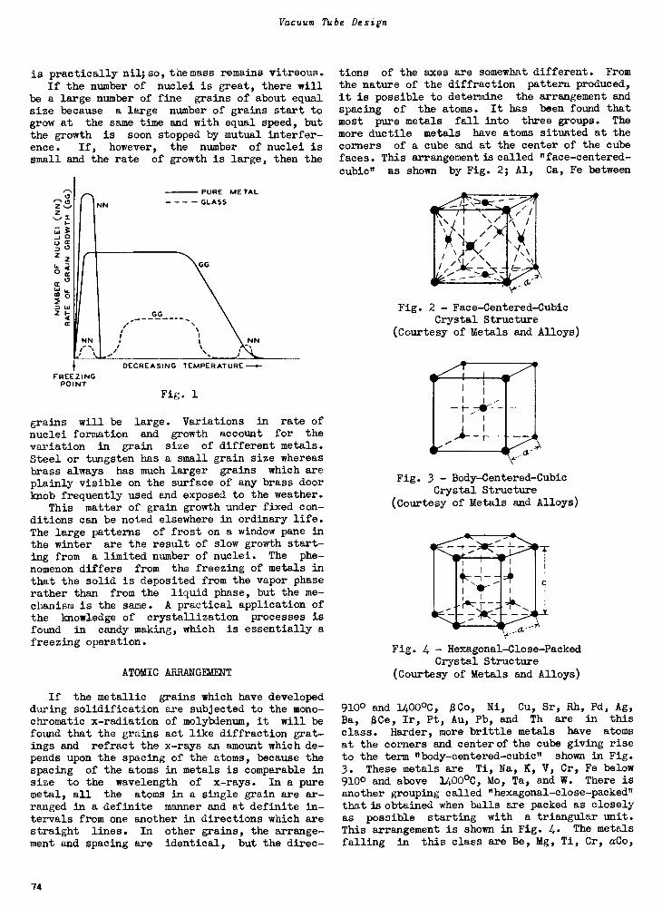
Vacuum Tube Design
is practically nil; so, the mass remains vitreous.
If the number of nuclei is great, there willbe a large number of fine grains of about equalsize because a large number of grains start togrow at the same time and with equal speed, butthe growth is soon stopped by mutual interfer-ence. If, however, the number of nuclei issmall and the rate of growth is large, then the
cr
z
FREEZINGPOINT
PURE METAL- - - - GLASS
NN
DECREASING TEMPERATURE
Fig. 1
grains will be large. Variations in rate ofnuclei formation and growth account for the
variation in grain size of different metals.Steel or tungsten has a small grain size whereasbrass always has much larger grains which areplainly visible on the surface of any brass doorknob frequently used and exposed to the weather.
This matter of grain growth under fixed con-ditions can be noted elsewhere in ordinary life.The large patterns of frost on a window pane inthe winter are the result of slow growth start-ing from a limited number of nuclei. The phe-
nomenon differs from the freezing of metals inthat the solid is deposited from the vapor phaserather than from the liquid phase, but the me-chanism is the same. A practical application ofthe knowledge of crystallization processes is
found in candy making, which is essentially afreezing operation.
ATOMIC ARRANGEMENT
If the metallic grains which have developedduring solidification are subjected to the mono-chromatic x-radiation of molybdenum, it will befound that the grains act like diffraction grat-ings and refract the x-rays an amount which de-pends upon the spacing of the atoms, because thespacing of the atoms in metals is comparable insize to the wavelength of x-rays. In a puremetal, all the atoms in a single grain are ar-ranged in a definite manner and at definite in-tervals from one another in directions which arestraight lines. In other grains, the arrange-ment and spacing are identical, but the direc-
tions of the axes are somewhat different. Fromthe nature of the diffraction pattern produced,
it is possible to determine the arrangement andspacing of the atoms. It has been found thatmost pure metals fall into three groups. The
more ductile metals have atoms situated at thecorners of a cube and at the center of the cubefaces. This arrangement is called "face -centered -
cubic" as shown by Fig. 2; Al, Ca, Fe between
Yr"
Fig. 2 - Face -Centered -CubicCrystal Structure
(Courtesy of Metals and Alloys)
Fig. 3 - Body -Centered -CubicCrystal Structure
(Courtesy of Metals and Alloys)
Fig. 4 - Hexagonal -Close -PackedCrystal Structure
(Courtesy of Metals and Alloys)
9100 and 1400°C, OCo, Ni, Cu, Sr, Rh, Pd, Ag,Ba, OCe, Ir, Pt, Au, Pb, and Th are in this
class. Harder, more brittle metals have atoms
at the corners and center of the cube giving riseto the term "body -centered -cubic" shown in Fig.
3. These metals are Ti, Na, K, V, Cr, Fe below9100 and above 1400°C, Mo, Ta, and W. There isanother grouping called "hexagonal -close -packed"that is obtained when balls are packed as closelyas possible starting with a triangular unit.This arrangement is shown in Fig. 4. The metals
falling in this class are Be, Mg, Ti, Cr, aCo,
74
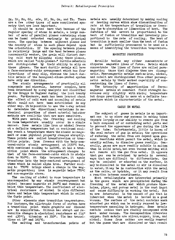
Umbreit: Metallurgical Principles
Zn, Zr, Ru, Cd, aCe, Hf, Rn, Os, and Th. Thereare a few other types of more complicated sym-metry that are less important.
It should be noted here that because of theregular spacing of atoms in metals, a large num-ber of sets of parallel planes containing atomscan be found oriented variously to principalaxes. The spacing between adjacent planes andthe density of atoms in each plane depend uponthe orientation. If the spacing between planesis relatively large and the bond between planesconsequently weaker, the grain will distort dur-ing cold work by slipping along these planes,which are called "slip -planes." Ductile materialsare distinguished by their ability to slip onthese planes. The most ductile metals all havea face -centered -cubic arrangement which has fourdirections of easy slip, whereas the least duc-tile metals of the hexagonal -close -packed systemhave only one direction.
The atomic arrangements of practically allcompounds and minerals, however complex, havebeen determined by x-ray analysis and classifiedby the Braggs in England during the last twentyyears. Furthermore, much has been learned aboutthe effect of cold work and annealing of metalswhich could not have been established in anyother way. It is possible to use the x-ray methodto determine the directional variations in me-chanical properties of sheet material but othermethods are available that are more sensitive.
With pure metals, the freezing and coolingto room temperature usually occur in a simplemanner. Some metals like iron or nickel freezeat a definite temperature but on continued cool-ing reach a temperature where the atomic arrange-ment or some physical property changes abruptly.These points are called transformation or tran-sition points. Iron freezes with the body -cen-tered -cubic atomic arrangement at 1530°C but,with continued cooling to 1400°C, it has a tran-sition point where the arrangement changes tothat of the face -centered -cubic which is stabledown to 910°C. At this temperature, it againtransforms into the body -centered arrangement ofatoms which is called alpha iron. Further cool-ing to 770°C brings about a change in the mag-netic properties; iron is magnetic below 770°Cand non-magnetic above.
The cooling of nickel to room temperature isunaccompanied by any atomic rearrangement butnickel becomes magnetic at 360°C and remains sobelow this temperature. The coefficient of elec-trical resistance of nickel is also differentabove and below this temperature which is calledthe Curie point.
Other elements show transition temperatures.For instance, the allotropic forms of carbon havea transition point where graphite and diamondare in equilibrium. Silicon has abrupt and re-versible changes in electrical resistance at 214°and 435°C; titanium at 310°. Tin has transi-tions at 180 and 161°C.
The melting and transformation points of
metals are usually determined by making coolingor heating curves which show discontinuities ofrate at the temperature of transition or freez-ing due to absorption or liberation of heat. Theduration of the arrest is proportional to theheat of fusion or transition and inversely pro-portional to the rate of cooling. The heat oftransition is much smaller than the heat of fusionbut is sufficiently pronounced to be used as ameans of identifying the transition temperature.
MAGNETIC PROPERTIES
Metallic bodies may either concentrate ordisperse magnetic lines of force. Metals whichconcentrate the lines of force are called para-magnetic; those that disperse them are diamag-netic. Ferromagnetic metals such as iron, nickel,and cobalt are distinguished from other paramag-netic metals by their marked capability of con-centrating the lines of force.
The intensity of magnetization of ferro-magnetic metals at constant field strength de-creases only slightly with rising temperaturebut drops practically to zero at a definite tem-perature which is characteristic of the metal.
GASES IN METAL
The subject of gases in metals is an import-ant one to us since our success in making tubesdepends largely on our ability to remove gas froma bulb composed of or containing metal parts andto prevent the appearance of gas during the lifeof the tube. Unfortunately, little is known ofthe real nature of gas in metals; the operationsof reducing the metal from ore depend upon gas-eous reactions which permit the metal, which isusually molten, to dissolve gases readily. Gen-erally, gases are more readily soluble in moltenthan in solid metal, but even vacuum melting willnot remove all the gas from metal. It appearsthat gas can be retained by metals in severalways that are difficult to differentiate. Gasmay be occluded or adsorbed on the surface, itmay bedissolved in the metal as air is dissolvedin water, it may be in combination with the metalas the oxide, or hydride, or it may result froma reaction between constituents.
Most metallurgists are interested primarilyin the gases which are precipitated during thefreezing of the metal and which produce blow-holes, pipes, and porous metal in the cast ingotand cause difficulty in working the metal. Butwe are interested in the amount of gas that isliberated when the metal is heated in a goodvacuum. The surface of the metal contains muchadsorbed gas which can be easily removed by low -temperature annealing in hydrogen. Some metalscontain oxides that are readily decomposed withheat under vacuum. The decomposition liberatesoxygen. Such metals are silver, copper, iron, andnickel. Gases from oxides are easily removedbut the gases that are dissolved or that result
75
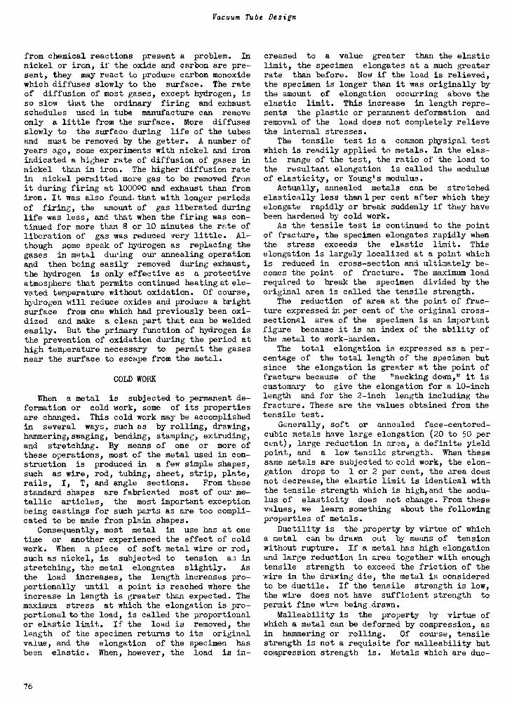
Vacuum Tube Design
from chemical reactions present a problem. In
nickel or iron, if the oxide and carbon are pre-sent, they may react to produce carbon monoxidewhich diffuses slowly to the surface. The rateof diffusion of most gases, except hydrogen, isso slow that the ordinary firing and exhaustschedules used in tube manufacture can removeonly a little from the surface. More diffusesslowly to the surface during life of the tubesand must be removed by the getter. A number ofyears ago, some experiments with nickel and ironindicated a higher rate of diffusion of gases innickel than in iron. The higher diffusion ratein nickel permitted more gas to be removed fromit during firing at 10000C and exhaust than fromiron. It was also found. that with longer periods
of firing, the amount of gas liberated duringlife was less, and that when the firing was con-tinued for more than 8 or 10 minutes the rate ofliberation of gas was reduced very little. Al-
though some speak of hydrogen as replacing thegases in metal during our annealing operationand then being easily removed during exhaust,
the hydrogen is only effective as a protectiveatmosphere that permits continued heating at ele-vated temperature without oxidation. Of course,hydrogen will reduce oxides and produce a brightsurface from one which had previously been oxi-dized and make a clean part that can be weldedeasily. But the primary function of hydrogen isthe prevention of oxidation during the period athigh temperature necessary to permit the gasesnear the surface to escape from the metal.
COLD WORK
When a metal is subjected to permanent de-formation or cold work, some of its propertiesare changed. This cold work may be accomplishedin several ways, such as by rolling, drawing,hammering, swaging, bending, stamping, extruding,and stretching. By means of one or more ofthese operations, most of the metal used in con-struction is produced in a few simple shapes,such as wire, rod, tubing, sheet, strip, plate,rails, I, T, and angle sections. From thesestandard shapes are fabricated most of our me-tallic articles, the most important exceptionbeing castings for such parts as are too compli-cated to be made from plain shapes.
Consequently, most metal in use has at onetime or another experienced the effect of coldwork. When a piece of soft metal wire or rod,such as nickel, is subjected to tension as instretching, the metal elongates slightly. As
the load increases, the length increases pro-portionally until a point is reached where theincrease in length is greater than expected. Themaximum stress at which the elongation is pro-portional to the load, is called the proportionalor elastic limit. If the load is removed, thelength of the specimen returns to its originalvalue, and the elongation of the specimen hasbeen elastic. When, however, the load is in-
creased to a value greater than the elasticlimit, the specimen elongates at a much greaterrate than before. Now if the load is relieved,the specimen is longer than it was originally bythe amount of elongation occurring above theelastic limit. This increase in length repre-sents the plastic or permanent deformation andremoval of the load does not completely relievethe internal stresses.
The tensile test is a common physipal testwhich is readily applied to metals. In the elas-tic range of the test, the ratio of the load tothe resultant elongation is called the modulusof elasticity, or Young's modulus.
Actually, annealed metals can be stretchedelastically less than l per cent after which theyelongate rapidly or break suddenly if they havebeen hardened by cold work.
As the tensile test is continued to the pointof fracture, the specimen elongates rapidly whenthe stress exceeds the elastic limit. Thiselongation is largely localized at a point whichis reduced in cross-section and ultimately be-comes the point of fracture. The maximum loadrequired to break the specimen divided by theoriginal area is called the tensile strength.
The reduction of area at the point of frac-ture expressed in per cent of the original cross-sectional area of the specimen is an importantfigure because it is an index of the ability ofthe metal to work -harden.
The total elongation is expressed as a per-centage of the total length of the specimen butsince the elongation is greater at the point offracture because of the "necking down," it iscustomary to give the elongation for a 10 -inchlength and for the 2 -inch length including thefracture. These are the values obtained from thetensile test.
Generally, soft or annealed face -centered -
cubic metals have large elongation (20 to 50 percent), large reduction in area, a definite yieldpoint, and a low tensile strength. When thesesame metals are subjected to cold work, the elon-gation drops to 1 or 2 per cent, the area doesnot decrease, the elastic limit is identical withthe tensile strength which is high,and the modu-lus of elasticity does not change. From thesevalues, we learn something about the followingproperties of metals.
Ductility is the property by virtue of whicha metal can be drawn out by means of tensionwithout rupture. If a metal has high elongationand large reduction in area together with enoughtensile strength to exceed the friction of thewire in the drawing die, the metal is consideredto be ductile. If the tensile strength is low,the wire does not have sufficient strength to
permit fine wire being drawn.Malleability is the property by virtue of
which a metal can be deformed by compression, asin hammering or rolling. Of course, tensilestrength is not a requisite for malleability butcompression strength is. Metals which are due -
76
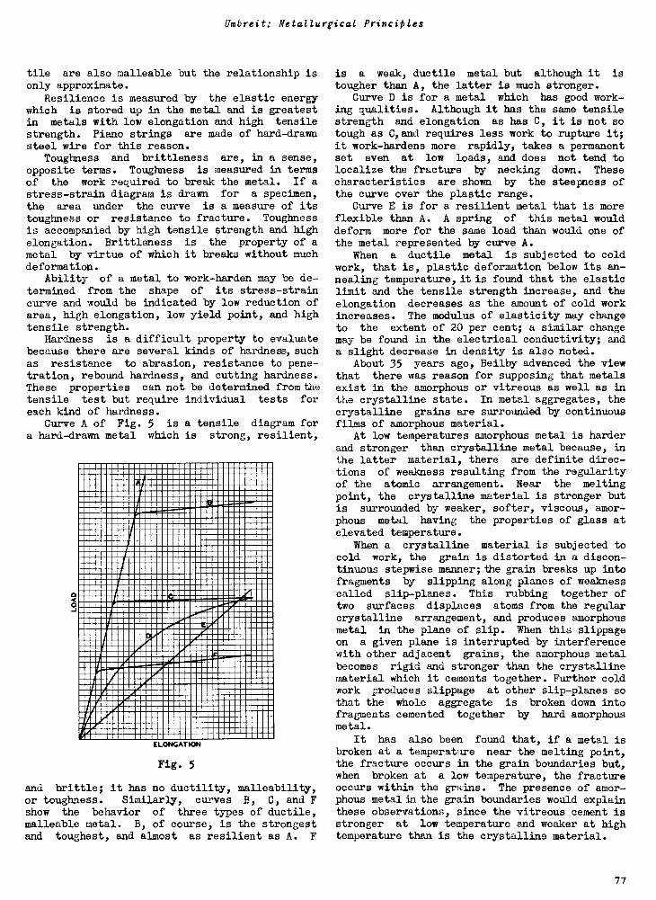
Umbreit: Metallurgical Principles
tile are also malleable but the relationship isonly approximate.
Resilience is measured by the elastic energywhich is stored up in the metal and is greatestin metals with low elongation and high tensilestrength. Piano strings are made of hard -drawnsteel wire for this reason.
Toughness and brittleness are, in a sense,opposite terms. Toughness is measured in termsof the work required to break the metal. If astress -strain diagram is drawn for a specimen,the area under the curve is a measure of itstoughness or resistance to fracture. Toughnessis accompanied by high tensile strength and highelongation. Brittleness is the property of ametal by virtue of which it breaks without muchdeformation.
Ability of a metal to work -harden may be de-termined from the shape of its stress -straincurve and would be indicated by low reduction ofarea, high elongation, low yield point, and hightensile strength.
Hardness is a difficult property to evaluatebecause there are several kinds of hardness, suchas resistance to abrasion, resistance to pene-tration, rebound hardness, and cutting hardness.These properties can not be determined from thetensile test but require individual tests foreach kind of hardness.
Curve A of Fig. 5 is a tensile diagram fora hard -drawn metal which is strong, resilient,
0
ELONGATION
Fig. 5
and brittle; it has no ductility, malleability,or toughness. Similarly, curves B, C, and Fshow the behavior of three types of ductile,malleable metal. B, of course, is the strongestand toughest, and almost as resilient as A. F
is a weak, ductile metal but although it is
tougher than A, the latter is much stronger.Curve D is for a metal which has good work-
ing qualities. Although it has the same tensilestrength and elongation as has C, it is not sotough as C,and requires less work to rupture it;it work -hardens more rapidly, takes a permanentset even at low loads, and does not tend tolocalize the fracture by necking down. Thesecharacteristics are shown by the steepness ofthe curve over the plastic range.
Curve E is for a resilient metal that is moreflexible than A. A spring of this metal woulddeform more for the same load than would one ofthe metal represented by curve A.
When a ductile metal is subjected to coldwork, that is, plastic deformation below its an-nealing temperature, it is found that the elasticlimit and the tensile strength increase, and theelongation decreases as the amount of cold workincreases. The modulus of elasticity may changeto the extent of 20 per cent; a similar changemay be found in the electrical conductivity; anda slight decrease in density is also noted.
About 35 years ago, Beilby advanced the viewthat there was reason for supposing that metalsexist in the amorphous or vitreous as well as inthe crystalline state. In metal aggregates, thecrystalline grains are surrounded by continuousfilms of amorphous material.
At low temperatures amorphous metal is harderand stronger than crystalline metal because, inthe latter material, there are definite direc-tions of weakness resulting from the regularityof the atomic arrangement. Near the meltingpoint, the crystalline material is stronger butis surrounded by weaker, softer, viscous, amor-phous metal having the properties of glass atelevated temperature.
When a crystalline material is subjected tocold work, the grain is distorted in a discon-tinuous stepwise manner; the grain breaks up intofragments by slipping along planes of weaknesscalled slip -planes. This rubbing together oftwo surfaces displaces atoms from the regularcrystalline arrangement, and produces amorphousmetal in the plane of slip. When this slippageon a given plane is interrupted by interferencewith other adjacent grains, the amorphous metalbecomes rigid and stronger than the crystallinematerial which it cements together. Further coldwork produces slippage at other slip -planes sothat the whole aggregate is broken down intofragments cemented together by hard amorphousmetal.
It has also been found that, if a metal isbroken at a temperature near the melting point,the fracture occurs in the grain boundaries but,when broken at a low temperature, the fractureoccurs within the grains. The presence of amor-phous metal in the grain boundaries would explainthese observations, since the vitreous cement isstronger at low temperature and weaker at hightemperature than is the crystalline material.
77
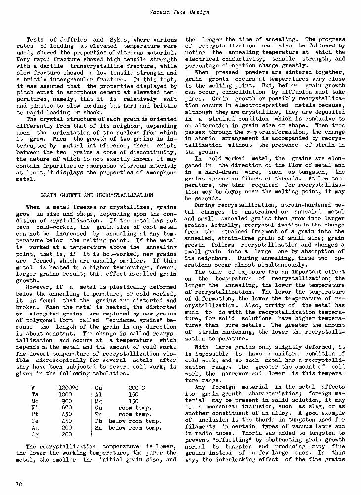
Vacuum Tube Design
Tests of Jeffries and Sykes, where variousrates of loading at elevated temperature wereused, showed the properties of vitreous material.Very rapid fracture showed high tensile strengthwith a ductile transcrystalline fracture, whileslow fracture showed a low tensile strength anda brittle intergranular fracture. In this test,it was assumed that the properties displayed bypitch exist in amorphous cement at elevated tem-peratures, namely, that it is relatively softand plastic to slow loading but hard and brittleto rapid loading or shock.
The crystal structure of each grain is orienteddifferently from that of its neighbor, dependingupon the orientation of the nucleus fiom whichit grew. When the growth of two grains is in-terrupted by mutual interference, there existsbetween the two grains a zone of discontinuity,the nature of which is not exactly known. It maycontain impurities or amorphous vitreous material;at least, it displays the properties of amorphousmetal.
GRAIN GROWTH AND RECRYSTALLIZATION
When a metal freezes or crystallizes, grainsgrow in size and shape, depending upon the con-dition of crystallization. If the metal has notbeen cold -worked, the grain size of cast metalcan not be increased by annealing at any tem-perature below the melting point. If the metalis worked at a temperature above the annealingpoint, that is, if it is hot -worked, new grainsare formed, which are usually smaller. If thismetal is heated to a higher temperature, fewer,larger grains result; this effect is called graingrowth.
However, if a metal is plastically deformedbelow the annealing temperature, or cold -worked,it is found that the grains are distorted andbroken. When the metal is heated, the distortedor elongated grains are replaced by new grainsof polygonal form called "equiaxed grains" be-cause the length of the grain in any directionis about constant. The change is called recrys-tallization and occurs at a temperature whichdepends on the metal and the amount of cold work.The lowest temperature of recrystallization vis-ible microscopically for several metals afterthey have been subjected to severe cold work, isgiven in the following tabulation.
W 1200°C Cu 200°CTa 1000 Al 150Mo 900 Mg 150Ni 600 Cu room temp.Pt 450 Zn room temp.Fe 450 Pb below room temp.Au 200 Sn below room temp.Ag 200
The recrystallization temperaturethe lower the working temperature, themetal, the smaller the initial grain
is lower,purer thesize, and
the longer the time of annealing. The progressof recrystallization can also be followed bynoting the annealing temperature at which theelectrical conductivity, tensile strength, andpercentage elongation change greatly.
When pressed powders are sintered together,grain growth occurs at temperatures very closeto the melting point. But, before grain growthcan occur, consolidation by diffusion must takeplace. Grain growth or possibly recrystalliza-tion occurs in electrodeposited metals because,although they are crystalline, they are depositedin a strained condition which is conducive toan alteration in grain size or shape. When ironpasses through the a-ry transformation, the changein atomic arrangement is accompanied by recrys-tallization without the presence of strain inthe grain.
In cold -worked metal, the grains are elon-gated in the direction of the flow of metal andin a hard -drawn wire, such as tungsten, the
grains appear as fibers or threads. At low tem-perature, the time required for recrystalliza-tion may be days; near the melting point, it maybe seconds.
During recrystallization, strain -hardened me-tal changes to unstrained or annealed metaland small annealed grains then grow into largergrains. Actually, recrystallization is the changefrom the strained fragment of a grain into theannealed, strain -free grain of small size; graingrowth follows recrystallization and changes asmall grain into a large one by absorption ofits neighbors. During annealing, these two op-
erations occur almost simultaneously.
The time of exposure has an important effecton the temperature of recrystallization; thelonger the annealing, the lower the temperatureof recrystallization. The lower the temperatureof deformation, the lower the temperature of re -crystallization. Also, purity of the metal hasmuch to do with the recrystallization tempera-ture, for solid solutions have higher tempera-tures than pure metals. The greater the amountof strain hardening, the lower the recrystalli-zation temperature.
With large grains only slightly deformed, itis impossible to have a uniform condition ofcold work; and so such metal has a recrystalli-zation range. The greater the amount of coldwork, the narrower and lower is this tempera-ture range.
Any foreign material in the metal affectsits grain growth characteristics; foreign ma-terial may be present in solid solution, it maybe a mechanical inclusion, such as slag, or asanother constituent of an alloy. A good exampleof inclusion is the thoria in tungsten used forfilaments in certain types of vacuum lamps andin radio tubes. Thoria was added to tungsten toprevent "offsetting" by obstructing grain growthnormal to tungsten and producing many fine
grains instead of a few large ones. In this
way, the interlocking effect of the fine grains
78
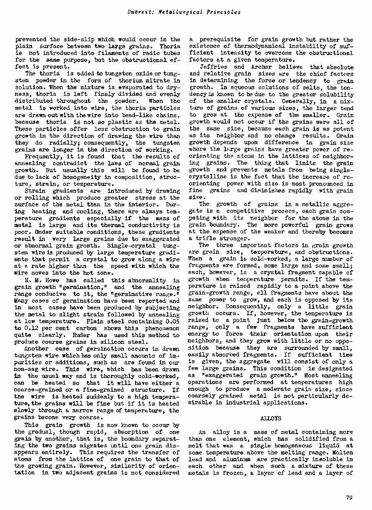
Umbreit: Metallurgical Principles
prevented the side -slip which would occur in theplain surface between two large grains. Thoriais not introduced into filaments of radio tubesfor the same purpose, but the obstructional ef-fect is present.
The thoria is added to tungsten oxide or tung-sten powder in the form of thorium nitrate insolution. When the mixture is evaporated to dry-ness, thoria is left finely divided and evenlydistributed throughout the powder. When themetal is worked into wire, the thoria particlesare drawn out with the wire into bead -like chains,because thoria is not so plastic as the metal.These particles offer less obstruction to graingrowth in the direction of drawing the wire thanthey do radially; consequently, the tungstengrains are longer in the direction of working.
Frequently, it is found that the results ofannealing contradict the laws of normal graingrowth. But usually this will be found to bedue to lack of homogeneity in composition, struc-ture, strain, or temperature.
Strain gradients are introduced by drawingor rolling which produce greater stress at thesurface of the metal than in the interior. Dur-ing heating and cooling, there are always tem-perature gradients especially if the mass ofmetal is large and its thermal conductivity ispoor. Under suitable conditions, these gradientsresult in very large grains due to exaggeratedor abnormal grain growth. Single -crystal tung-sten wire is produced by large temperature gradi-ents that permit a crystal to grow along a wireat a rate higher than the speed with which thewire moves into the hot zone.
H. M. Howe has called this abnormality ingrain growth "germination," and the annealingrange conducive to it, the "germinative range."Many cases of germination have been reported andin most cases have been produced by subjectingthe metal to slight strain followed by annealingat low temperature. Plain steel containing 0.05to 0.12 per cent carbon shows this phenomenonquite clearly. Ruder has used this method toproduce coarse grains in silicon steel.
Another case of germination occurs in drawntungsten wire which has only small amounts of im-purities or additions, such as are found in ournon -sag wire. This wire, which has been drawnin the usual way and is thoroughly cold -worked,can be heated so that it will have either acoarse -grained or a fine-grained structure. Ifthe wire is heated suddenly to a high tempera -ture,the grains will be fine but if it is heatedslowly through a narrow range of temperature, thegrains become very coarse.
This grain growth is now known to occur bythe gradual, though rapid, absorption of onegrain by another, that is, the boundary separat-ing the two grains migrates until one grain dis-appears entirely. This requires the transfer ofatoms from the lattice of one grain to that ofthe growing grain. However, similarity of orien-tation in two adjacent grains is not considered
a prerequisite for grain growth but rather theexistence of thermodynamical instability of suf-ficient intensity to overcome the obstructionalfactors at a given temperature.
Jeffries and Archer believe that absoluteand relative grain sizes are the chief factorsin determining the force or tendency to graingrowth. In aqueous solutions of salts, the ten-dencyis known to be due to the greater solubilityof the smaller crystals. Generally, in a mix-ture of grains of various sizes, the larger tendto grow at the expense of the smaller. Graingrowth would not occur if the grains were all ofthe same size, because each grain is as potentas its neighbor and no change results. Graingrowth depends upon difference in grain sizewhere the large grains have greater power of re-orienting the atoms in the lattices of neighbor-ing grains. The thing that limits the graingrowth and prevents metals from being single -crystalline is the fact that the increase of re-orienting power with size is most pronounced infine grains and diminishes rapidly with grainsize.
The growth of grains in a metallic aggre-gate is a competitive process, each grain com-peting with its neighbor for the atoms in thegrain boundary. The more powerful grain growsat the expense of the weaker and thereby becomesa trifle stronger.
The three important factors in grain growthare grain size, temperature, and obstructions.When a grain is cold -worked, a large number offragments are formed, some large and some small;each, however, is a crystal fragment capable ofgrowth when temperature permits. If the tem-perature is raised rapidly to a point above thegrain -growth range, all fragments have about thesame power to grow, and each is opposed by itsneighbor. Consequently, only a little graingrowth occurs. If, however, the temperature israised to a point just below the grain -growthrange, only a few fragments have sufficientenergy to force their orientation upon theirneighbors, and they grow with little or no oppo-sition because they are surrounded by small,easily absorbed fragments. If sufficient timeis given, the aggregate will consist of only afew large grains. This condition is designatedas "exaggerated grain growth." Most annealingoperations are performed at temperatures highenough to produce a moderate grain size, sincecoarsely grained metal is not particularly de-sirable in industrial applications.
ALLOYS
An alloy is a mass of metal containing morethan one element, which has solidified from amelt that was a single homogeneous liquid atsome temperature above the melting range. Moltenlead and aluminum are practically insoluble ineach other and when such a mixture of thesemetals is frozen, a layer of lead and a layer of
79
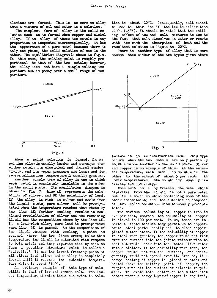
Vacuum Tube Design
aluminum are formed. This is no more an alloythan a mixture of oil and water is a solution.
The simplest form of alloy is the solid so-lution such as is formed when copper and nickelalloy. If an alloy of these two metals in anyproportion is inspected microscopically, it hasthe appearance of a pure metal because there isonly one phase, the solid solution of one in theother. The equilibrium diagram's shown in Fig.6.In this case, the melting point is roughly pro-portional to that of the two metals; however,the alloy does not have a single melting tem-perature but is pasty over a small range of tem-perature.
I083 *C
L 101J1D
SOLID
100
0
"e CuNi
1452 %
0
100
Fig. 6
When a solid solution is formed, the re-sulting alloy is usually harder and stronger thaneither metal; its electrical and thermal conduc-tivity, and its vapor pressure are less; and itsrecrystallization temperature is usually greater.
Another simple type of alloy is one in whicheach metal is completely insoluble in the otherin the solid state. Its equilibrium diagram isshown in Fig. 7. Line AE represents the solu-bility of silver, and BE the solubility of lead.If the alloy is rich in silver and cools fromthe liquid state, pure silver will be precipi-tated when the temperature reaches that shown bythe line AE; further cooling results in con-tinued precipitation of silver and the remainingliquid has the composition shown by the line AE.In a lead -rich alloy, pure lead is precipitatedwhen line BE is passed. As the composition ofthe liquid changes with cooling, a point isreached where the two lines cross; below thistemperature the liquid is saturated with respectto both metals and they separate side by side toform a peculiar structure which is called a"eutectic." It has the lowest freezing point ofall silver -lead alloys and no alloy is completelyfrozen until it reaches the eutectic tempera-ture which is about 31000.
An ordinary example of this type of solu-bility is that of ice and common salt. The low-est temperature at which these can exist in solu-
tion is about -20°C. Consequently, salt cannotbe used to thaw ice if the ice is colder than-20°C (-5°F). It should be noted that the chill-ing effect of ice and salt mixtures is due tothe fact that salt dissolves in water or reactswith ice with the absorption of heat and theresultant solution is liquid to -20°C.
There is another type of alloy that is morecommon than either of the two types given above
Fig. 7
because it is an intermediate case. This typeoccurs when the two metals are only partiallysoluble in one another in the solid state. Silverand copper is an example of this. At the eutec-tic temperature, each metal is solUble in theother to the extent of about 5 per cent. Atlower temperatures, the solubility usually de-creases but not always.
When such an alloy freezes, the metal whichseparates from the liquid is not a pure metalbut is a solid solution containing some of theother constituent; and the eutectic is composedof two solid solutions simultaneously precipi-tated.
The maximum solubility of copper in iron is3.4 per cent, whereas the solubility of copperin nickel is 100 per cent. To us, these are im-portant facts because they permit us to copper -braze steel parts easily and to clean copper -plated button stems. If the solubility of copperin steel were greater, the copper would not flowover the surface into the joints which we wish toseal but would soak into the metal like waterinto a blotter. If the solubility were zero, thecopper would not wet the surface, and conse-quently, would not spread over it. Even so, if aheavy coating of copper is placed on steel andheated above the melting point of copper, thesurplus runs off the surface or collects in pud-dles. To avoid this action on the button -stemheader where a heavy layer of copper is required,
80
Umbreit: Metallurgical Principles
the steel is first plated with a layer of nickelheavy enough to absorb all the copper and pre-vent the puddles which would otherwise form. Thenickel resists oxidation during stem -making
better than copper alone, but it could not becleaned up later if the copper were not present.During stem -making, the copper is more rapidlyoxidized at the surface of the metal, and is
easily reduced to metal during the hydrogencleaning operation which leaves a bright copper -colored surface.
It may be noted that molybdenum cannot bebrazed in hydrogen with copper, because copper isinsoluble in molybdenum and there is no tendencytoward wetting of molybdenum by copper.
Ordinary solder, a lead -tin alloy, is a
similar case and brings up an important point.With the exception of the 65% Sn - 35% Pb alloywhich has the eutectic composition,no other com-position of these alloys has a freezing point.
They have freezing ranges and are pasty above
1810C. This means that in soldering a joint, itis necessary to heat it above the pasty range(above 24000 for a 40-60 solder) but the finishedjoint should never be heated above 1800C, be-cause liquid metal is present above 180°C andweakens the joint. The wiped joints made on
lead pipes by plumbers were only possible be-cause they used a solder low in tin which had along pasty range that permitted molding thejoint by wiping.
81
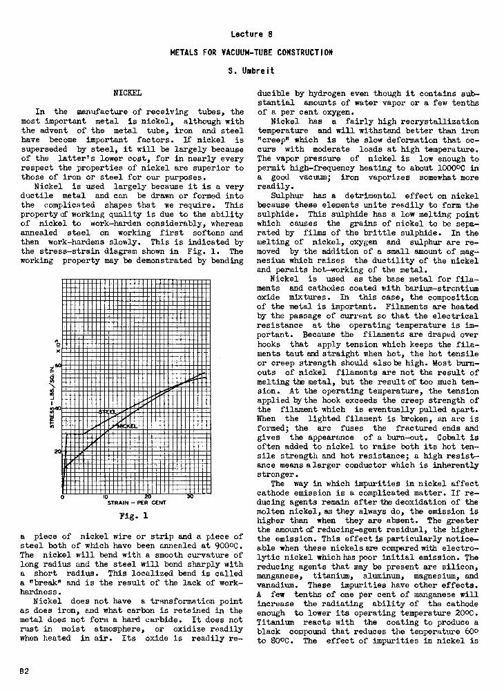
Lecture 8
METALS FOR VACUUM -TUBE CONSTRUCTION
S. Umbreit
NICKEL
In the manufacture of receiving tubes, themost important metal is nickel, although withthe advent of the metal tube, iron and steelhave become important factors. If nickel is
superseded by steel, it will be largely becauseof the latter's lower cost, for in nearly everyrespect the properties of nickel are superior tothose of iron or steel for our purposes.
Nickel is used largely because it is a veryductile metal and can be drawn or formed intothe complicated shapes that we require. Thisproperty of working quality is due to the abilityof nickel to work -harden considerably, whereasannealed steel on working first softens andthen work -hardens slowly. This is indicated bythe stress -strain diagram shown in Fig. 1. Theworking property may be demonstrated by bending
0X
60
1
20
a.
0 10 20STRAIN - PER CENT
Fig. 1
30
a piece of nickel wire or strip and a piece ofsteel both of which have been annealed at 9000C.The nickel will bend with a smooth curvature oflong radius and the steel will bend sharply witha short radius. This localized bend is calleda "break" and is the result of the lack of work -hardness.
Nickel does not have a transformation pointas does iron, and what carbon is retained in themetal does not form a hard carbide. It does notrust in moist atmosphere, or oxidize readilywhen heated in air. Its oxide is readily re-
ducible by hydrogen even though it contains sub-stantial amounts of water vapor or a few tenthsof a per cent oxygen.
Nickel has a fairly high recrystallizationtemperature and will withstand better than iron"creep" which is the slow deformation that oc-curs with moderate loads at high temperature.The vapor pressure of nickel is low enough topermit high -frequency heating to about 10000C ina good vacuum; iron vaporizes somewhat morereadily.
Sulphur has a detrimental effect on nickelbecause these elements unite readily to form thesulphide. This sulphide has a low melting pointwhich causes the grains of nickel to be sepa-rated by films of the brittle sulphide. In themelting of nickel, oxygen and sulphur are re-moved by the addition of a small amount of mag-nesium which raises the ductility of the nickeland permits hot -working of the metal.
Nickel is used as the base metal for fila-ments and cathodes coated with barium -strontiumoxide mixtures. In this case, the compositionof the metal is important. Filaments are heatedby the passage of current so that the electricalresistance at the operating temperature is im-portant. Because the filaments are draped overhooks that apply tension which keeps the fila-ments taut and straight when hot, the hot tensileor creep strength should also be high. Most burn-outs of nickel filaments are not the result ofmelting the metal, but the result of too much ten-sion. At the operating temperature, the tensionapplied by the hook exceeds the creep strength ofthe filament which is eventually pulled apart.When the lighted filament is broken, an arc isformed; the arc fuses the fractured ends andgives the appearance of a burn -out. Cobalt isoften added to nickel to raise both its hot ten-sile strength and hot resistance; a high resist-ance means a larger conductor which is inherentlystronger.
The way in which impurities in nickel affectcathode emission is a complicated matter. If re-ducing agents remain after the deoxidation of themolten nickel, as they always do, the emission ishigher than when they are absent. The greaterthe amount off reducing -agent residual, the higherthe emission. This effect is particularly notice-able when these nickels are compared with electro-lytic nickel which has poor initial emission. Thereducing agents that may be present are silicon,manganese, titanium, aluminum, magnesium, andvanadium. These impurities have other effects.A few tenths of one per cent of manganese willincrease the radiating ability of the cathodeenough to lower its operating temperature 200C.Titanium reacts with the coating to produce ablack compound that reduces the temperature 600to 800C. The effect of impurities in nickel is
82
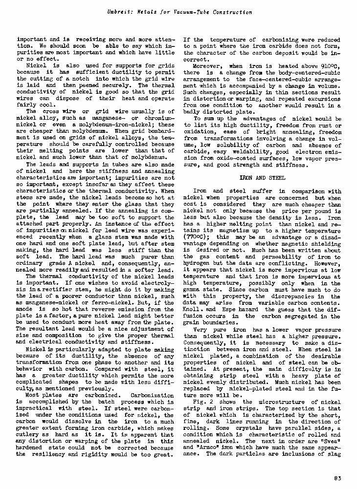
Umbreit: Metals for Vacuum -Tube Construction
important and is receiving more and more atten-tion. We should soon be able to say which im-purities are most important and which have littleor no effect.
Nickel is also used for supports for gridsbecause it has sufficient ductility to permitthe cutting of a notch into which the grid wireis laid and then peened securely. The thermalconductivity of nickel is good so that the gridwires can dispose of their heat and operatefairly cool.
The cross wire or grid wire usually is ofnickel alloy, such as manganese- or chromium -nickel or even a molybdenum -iron -nickel; theseare cheaper than molybdenum. When grid bombard-ment is used on grids of nickel alloys, the tem-perature should be carefully controlled becausetheir melting points are lower than that ofnickel and much lower than that of molybdenum.
The leads and supports in tubes are also madeof nickel and here the stiffness and annealingcharacteristics am important; impurities are notso important, except insofar es they affect thesecharacteristics or the thermal conductivity. Whenstems are made, the nickel leads become so hot atthe point where they enter the glass that theyare partially annealed. If the annealing is com-plete, the lead may be too soft to support theattached part properly. An instance of the effectof impuritiescn. nickel for lead wire was experi-enced recently when a glass stem was made withone hard and one soft plate lead, but after stemmaking, the hard lead was less stiff than thesoft lead. The hard lead was much purer thanordinary grade A nickel and, consequently, an-nealed more readilyemdresultedin a softer lead.
The thermal conductivity of the nickel leadsis important. If one wishes to avoid electroly-sis inarectifier stem, he might do it by makingthe lead of a poorer conductor than nickel, suchas manganese nickel or ferro-nickel. But, if theanode is so hot that reverse emission from theplate is a factor, a pure nickel lead might betterbe used to conduot more heat away from the plate.The resultant lead would be a nice adjustment ofsize and composition to give the proper thermaland electrical conductivity and stiffness.
NickeliS particularly adapted to plate makingbecause of its ductility, the absence of anytransformation from one phase to another and itsbehavior with carbon. Compared with steel, ithas a greater ductility which permits the morecomplicated shapes to be made with less diffi-culty, as mentioned previously.
Most plates are carbonized. Carbonizationis accomplished by the batch process which isimpractical with steel. If steel were carbon-ized under the conditions used for nickel, thecarbon would dissolve in the iron to a muchgreater extent forming iron carbide, which makescutlery as hard as it is. It is apparent thatany distortion or warping of the plate in thishardened state could not be corrected becausethe resiliency and rigidity would be too great.
If the temperature of carbonizing were reducedto a point where the iron carbide does not form,the character of the carbon deposit would be in-correct.
Moreover, when iron is heated above 9100C,there is a change from the body -centered -cubicarrangement to the face -centered -cubic arrange-ment which is accompanied by a change in volume.Such changes, especially in thin sections resultin distortion or warping, and repeated excursionsfrom one condition to another would result in abadly distorted plate.
To sum up the advantages of nickel would beto list its high ductility, freedom from rust oroxidation, ease of bright annealing, freedomfrom transformations involving a change in vol-ume, low solubility of carbon and absence ofcarbide, easy weldability, good electron emis-sion from oxide -coated surfaces, low vapor pres-sure, and good strength and stiffness.
IRON AND STEEL
Iron and steel suffer in comparison withnickel when properties are concerned but whencost is considered they are much cheaper thannickel not only because the price per pound isless but also because the density is less. Ironhas a higher melting point than nickel and re-tains its magnetism up to a higher temperature(7700C); this may be an advantage or a disad-vantage depending on whether magnetic shieldingis desired or not. Much has been written aboutthe gas content and permeability of iron tohydrogen but the data are conflicting. However,it appears that nickel is more impervious at lowtemperature and that iron is more impervious athigh temperature, possibly only when in thegamma state. Since carbon must have much to dowith this property, the discrepancies in thedata may arise from variable carbon contents.Knoll. and Espe hazard the guess that the dif-fusion occurs in the carbon segregated in thegrain boundaries.
Very pure iron has a lower vapor pressurethan nickel while steel has a higher pressure.Consequently, it is necessary to make a dis-tinction between iron and steel. When steel isnickel plated, a combination of the desirableproperties of nickel and of steel can be ob-tained. At present, the main difficulty is inobtaining strip steel with a heavy plate ofnickel evenly distributed. Much nickel has beenreplaced by nickel -plated steel and in the fu-ture more will be.
Fig. 2 shows the microstructure of nickelstrip and iron strips. The top section is thatof nickel which is characterized by the short,fine, dark lines running in the direction ofrolling. Some crystals have parallel sides, acondition which is characteristic of rolled andannealed nickel. The next in order are ftSvea"and "Armco" hon which have much the same appear-ance. The dark particles are inclusions of slag
83
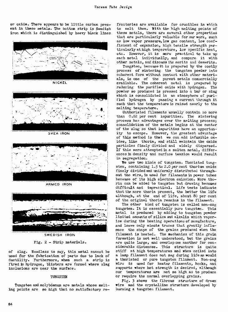
Vacuum Tube Design
or oxide. There appears to be little carbon pres-ent in these metals. The bottom strip is Swedishiron which is distinguished by heavy black lines
SVEA IRON
ARMCO IRON
%.
SWEDISH IRON
Fig. 2 - Strip materials.
of slag. Needless to say, this metal cannot beused for the fabrication of parts due to lack ofductility. Furthermore, when such a strip isfired in hydrogen, blisters are formed where slaginclusions are near the surface.
TUNGSTEN
Tungsten and molybdenum are metals whose melt-ing points are so high that no satisfactory re-
fractories are available for crucibles in whichto melt them. With the high melting points ofthese metals, there are several other propertiesthat are particularly valuable for our work, suchas low vapor pressure, low gas content, low coef-ficient of expansion, high tensile strength par-ticularly at high temperature, low specific heat,etc. However, it is more practical to take upeach metal individually, and compare it withother metals, and discuss its merits and demerits.
Tungsten, because it is prepared by the costlyprocess of sintering the tungsten powder intocoherent form without contact with other materi-als, is one of the purest metals commerciallyavailable. The coherent metal is prepared byreducing the purified oxide with hydrogen. Thepowder so produced is pressed into a bar or slugwhich is consolidated in an atmosphere of puri-fied hydrogen by passing a current through itsuch that the temperature is raised nearly to themelting temperature.
Unthoriated filaments usually contain no morethan 0.02 per cent impurities. The sinteringprocess has advantages over the melting process;consolidation of the metals begins at the centerof the slug so that impurities have an opportun-ity to escape. However, the greatest advantageof this method is that we can add infusible ox-ides, like thoria, and still maintain the oxideparticles finely divided and widely dispersed.If this were attempted in a molten metal, differ-encesin density and surface tension would resultin segregation.
We use two kinds of tungsten. Thoriated tung-sten, containing 1.5 to 2.0 per cent thorium oxidefinely divided and uniformly distributed through-out the wire, is used for filaments in power tubesbecause of its high electron emission. More tho-ria can be added to tungsten but drawing becomesdifficult and impractical. Life tests indicatethat the more thoria present, the better the lifealthough, at the end of life, about 80 per centof the original thoria remains in the filament.
The other kind of tungsten is called non -sagtungsten. It is essentially pure tungsten. Thismetal is produced by adding to tungsten powderlimited amounts of silica and alkalis which vapor-ize during the heating operations of manufacture,and leave only minute traces that greatly influ-ence the shape of the grains produced when the
filament is heated. The mechanism of this grainformation is not well understood, but the grainsare quite large, and overlap one another for con-siderable distances. This structure is quitestiff at high temperatures and when coiled intoa lamp filament does not sag during life as woulda thoriated or pure tungsten filament. Non -sag
wire is used for heater filaments, hooks, andsupports where hot strength is desired, althoughour temperatures are not so high as to produceor require the normal overlapping grains.
Fig. 3 shows the fibrous structure of drawnwire and the crystalline structure developed byburning a tungsten filament.
84
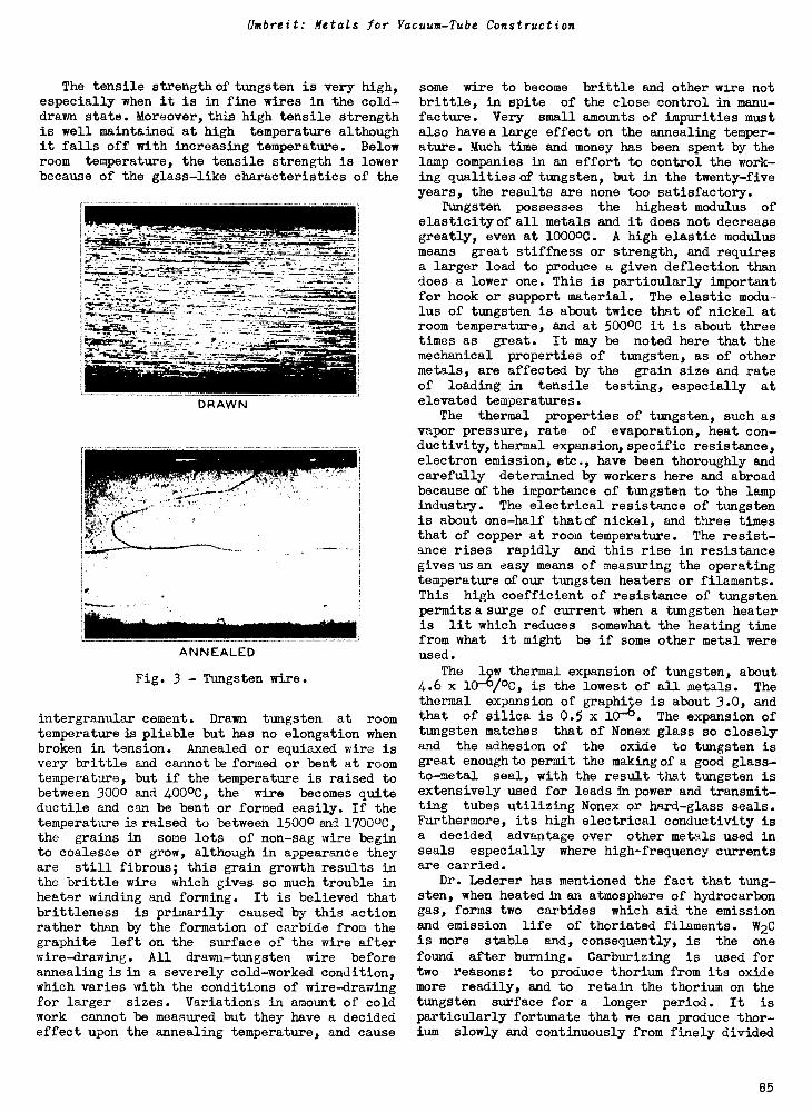
Umbreit: Metals for Vacuum -Tube Construction
The tensile strength of tungsten is very high,especially when it is in fine wires in the cold -drawn state. Moreover, this high tensile strengthis well maintained at high temperature althoughit falls off with increasing temperature. Belowroom temperature, the tensile strength is lowerbecause of the glass -like characteristics of the
44.4-.44
,_-
11101.,
DRAWN
ANNEALED
Fig. 3 - Tungsten wire.
intergranular cement. Drawn tungsten at roomtemperature is pliable but has no elongation whenbroken in tension. Annealed or equiaxed wire isvery brittle and cannot be formed or bent at roomtemperature, but if the temperature is raised tobetween 3000 and 4000C, the wire becomes quiteductile and can be bent or formed easily. If thetemperature is raised to between 15000 and 17000C,the grains in some lots of non -sag wire beginto coalesce or grow, although in appearance theyare still fibrous; this grain growth results inthe brittle wire which gives so much trouble inheater winding and forming. It is believed thatbrittleness is primarily caused by this actionrather than by the formation of carbide from thegraphite left on the surface of the wire afterwire -drawing. All drawn -tungsten wire beforeannealing is in a severely cold -worked condition,which varies with the conditions of wire -drawingfor larger sizes. Variations in amount of coldwork cannot be measured but they have a decidedeffect upon the annealing temperature, and cause
some wire to become brittle and other wire notbrittle, in spite of the close control in manu-facture. Very small amounts of impurities mustalso havea large effect on the annealing temper-ature. Much time and money has been spent by thelamp companies in an effort to control the work-ing qualities of tungsten, but in the twenty-fiveyears, the results are none too satisfactory.
Tungsten possesses the highest modulus ofelasticity of all metals and it does not decreasegreatly, even at 10000C. A high elastic modulusmeans great stiffness or strength, and requiresa larger load to produce a given deflection thandoes a lower one. This is particularly importantfor hook or support material. The elastic modu-lus of tungsten is about twice that of nickel atroom temperature, and at 5000C it is about threetimes as great. It may be noted here that themechanical properties of tungsten, as of othermetals, are affected by the grain size and rateof loading in tensile testing, especially atelevated temperatures.
The thermal properties of tungsten, such asvapor pressure, rate of evaporation, heat con -ductivity,thermal expansion, specific resistance,electron emission, etc., have been thoroughly andcarefully determined by workers here and abroadbecause of the importance of tungsten to the lampindustry. The electrical resistance of tungstenis about one-half that cC nickel, and three timesthat of copper at room temperature. The resist-ance rises rapidly and this rise in resistancegives us an easy means of measuring the operatingtemperature of our tungsten heaters or filaments.This high coefficient of resistance of tungstenpermits a surge of current when a tungsten heateris lit which reduces somewhat the heating timefrom what it might be if some other metal wereused.
The low thermal expansion of tungsten, about4.6 x 10-6/00, is the lowest of all metals. Thethermal expansion of graphite is about 3.0, andthat of silica is 0.5 x 10⁻⁶. The expansion oftungsten matches that of Nonex glass so closelyand the adhesion of the oxide to tungsten isgreat enough to permit the making of a good glass -to -metal seal, with the result that tungsten isextensively used for leads in power and transmit-ting tubes utilizing Nonex or hard -glass seals.Furthermore, its high electrical conductivity isa decided advantage over other metals used inseals especially where high -frequency currentsare carried.
Dr. Lederer has mentioned the fact that tung-sten, when heated in an atmosphere of hydrocarbongas, forms two carbides which aid the emissionand emission life of thoriated filaments. W2Cis more stable and, consequently, is the one
found after burning. Carburizing is used fortwo reasons: to produce thorium from its oxidemore readily, and to retain the thorium on thetungsten surface for a longer period. It isparticularly fortunate that we can produce thor-ium slowly and continuously from finely divided
85
Vacuum Tube Design
thoria, because this process assures that thefilament will have a constantly replenished sur-face of thorium atoms. If this were not thecase, an alloy of thorium and tungsten would veryrapidly lose its thorium and become depleted,because the thorium would reach the surface muchmore rapidly than a monatomic film could evapo-rate, with the result that a polyatomic layerwould be formed and this would evaporate morerapidly than a monatomic layer. When a carbur-ized tungsten filament is burned, the tungstencarbide disappears at a greater rate than can beaccounted for by the reaction between thoria andthe carbide. This disappearance must resultfrom the decomposition of the carbide and thevaporization of carbon. A filament in a 50 -watttube operated for 500 hours at normal voltagewould contain no carbide at the hottest part,although the emission would show no serious dim-inution. Apparently, the effect of the carbideremains after its disappearance. The rate atwhich the carbide disappears is a function ofnot only the getter action but also the amountof magnesium present.
MOLYBDENUM
In less pronounced form, molybdenum has thecharacteristic properties of tungsten and conse-quently, is used less widely in the lamp industry.However, in the drawn state, it possesses a re-spectable amount of ductility and elongation; evenafter prolonged heating at elevated temperature,the wire is not brittle. For this reason alone,it has applications where it is preferable totungsten. We are using molybdenum for supporthooks, support rods, grid wire, filaments, plates,seal -in -wire, getter tabs, and furnace windingsfor high -temperature work. In power and transmit-ting tubes, much molybdenum is used where nickelis used in receiving tubes.
Because of its superior working properties,drawing, rolling, and forming of molybdenum canbe performed at room temperature, whereas tung-sten must be worked hot. In the cold -drawnstate, its properties are similar to those oftungsten; when annealed, molybdenum behaves likethe ordinary ductile metal.
At one time, the greatest use of molybdenumin receiving tubes was for grid wires, but nowit has been largely replaced by cheaper nickelalloys which also have some other advantages.Molybdenum is an excellent grid wire for severalreasons. Its thermal conductivity is high so
that heat is transmitted to the support rodsreadily, it has good hot strength so that it doesnot distort when subjected to grid bombardment,it possesses ample ductility for making gridswhich will retain their shapes, its thermal ex-pansion is low so that there is less likelihoodof buckling in the tube if the grid is bombarded,and the melting point is high enough to permitthorough degassing. Six or seven years ago, mo-lybdenum was used almost exclusively for grid
wires but now its use in receiving tubes is limitedto a few flat grids where other materials cannot be substituted. There are several reasonsfor this change to nickel alloys. We found thatmanganese nickel,because of its contact potentialor lower grid emission, enabled us to obtaingreater power output from tubes like the 45, 46,and 47. Then, too, more receiving types weremade with cylindrical grids which do not requirethe hot strength of molybdenum and so nickelalloys were cheaper and equally satisfactory.Furthermore, molybdenum oxidizes readily and itshighest oxide is distinctly volatile even at at-mospheric pressures. During the exhaust of atube, a molybdenum grid may become oxidized andbe subjected to positive ion bombardment if gasis present. Under these conditions, molybdenumor its lower oxides are deposited upon the cathodewhich then loses its emission. For these reasons,little molybdenum is now used for grid wires. Ithas been replaced by manganese nickel, chromenickel, and even steel.
Molybdenum is also used in making supporthooks and leads or tips for tungsten filaments,where the superior mechanical properties of mo-lybdenum are required. In power tubes, molybde-num tips are used between the tungsten filamentand the nickel lead not only for the sake of theadded hot strength at the operating temperatureand the lower vapor pressure, but also becausetungsten (and also molybdenum for that matter)in contact with nickel would form a eutecticwhich would fuse and fail at about 13000C.
With the advent of metal tubes, molybdenumbecameen important seal -in metal for hard glass,such as 705AJ or 705BA which is used with Fernicoeyelets. The thermal expansion of molybdenum islinear and does not match that of the glass aswell as does that of Fernico or Kovar, but themuch better electrical conductivity of molybdenumgives it a distinct advantage. The electricalresistance of Fernico is high. Because of thesmall size of the eyelets and short path in theglass between eyelet and lead, the latter must bekept as small as possible and be made of a metalhaving good conductivity.
When we started to make metal tubes withmolybdenum seals, we felt it necessary to firethe nickel -molybdenum -nickel leads in hydrogenfor one hour at 11000C in order to remove fromthe surface the carbon that gave gassy seals.This treatment was disadvantageous and evendetrimental. At 11000, the nickel became ex-ceedingly soft and sintered the leads togetherso that it required a large number of girls toseparate them and to straighten them by rolling.Also, some lots of molybdenum would recrystal-lize near the nickel welds and become so brittlethat the leads were useless. We soon found thatthe firing of these leads was unnecessary if thewire before weldmaking was properly cleaned byetching away the outer surface.
Molybdenum support wires are used in powertubes because of their greater stiffness par -
86
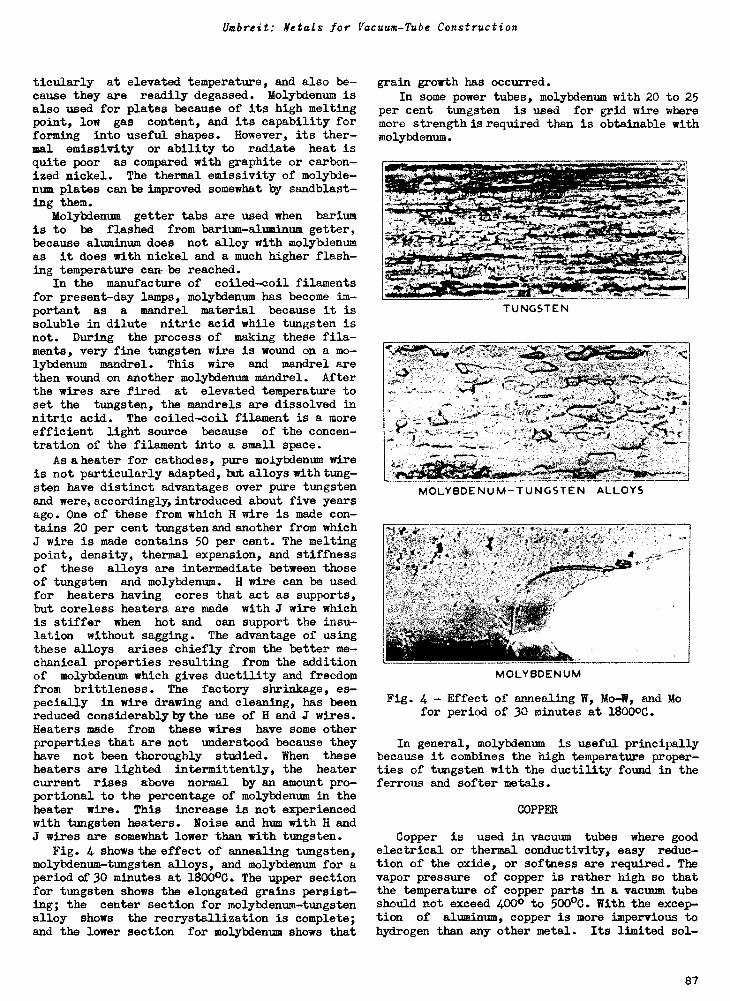
Umbreit: Metals for Vacuum -Tube Construction
ticularly at elevated temperature, and also be-cause they are readily degassed. Molybdenum isalso used for plates because of its high meltingpoint, low gas content, and its capability forforming into useful shapes. However, its ther-mal emissivity or ability to radiate heat isquite poor as compared with graphite or carbon-ized nickel. The thermal emissivity of molybde-num plates cants improved somewhat by sandblast-ing them.
Molybdenum getter tabs are used when bariumis to be flashed from barium -aluminum getter,because aluminum does not alloy with molybdenumas it does with nickel and a much higher flash-ing temperature canbe reached.
In the manufacture of coiled -coil filamentsfor present-day lamps, molybdenum has become im-portant as a mandrel material because it issoluble in dilute nitric acid while tungsten isnot. During the process of making these fila-ments, very fine tungsten wire is wound on a mo-lybdenum mandrel. This wire and mandrel arethen wound on another molybdenum mandrel. Afterthe wires are fired at elevated temperature toset the tungsten, the mandrels are dissolved innitric acid. The coiled -coil filament is a moreefficient light source because of the concen-tration of the filament into a small space.
As a heater for cathodes, pure molybdenum wireis not particularly adapted, but alloys with tung-sten have distinct advantages over pure tungstenand were, accordingly, introduced about five yearsago. One of these from which H wire is made con-tains 20 per cent tungsten and another from whichJ wire is made contains 50 per cent. The meltingpoint, density, thermal expansion, and stiffnessof these alloys are intermediate between thoseof tungsten and molybdenum. H wire can be usedfor heaters having cores that act as supports,but coreless heaters are made with J wire whichis stiffer when hot and can support the insu-lation without sagging. The advantage of usingthese alloys arises chiefly from the better me-chanical properties resulting from the additionof molybdenum which gives ductility and freedomfrom brittleness. The factory shrinkage, es-pecially in wire drawing and cleaning, has beenreduced considerably by the use of H and J wires.Heaters made from these wires have some otherproperties that are not understood because theyhave not been thoroughly studied. When theseheaters are lighted intermittently, the heatercurrent rises above normal by an amount pro-portional to the percentage of molybdenum in theheater wire. This increase is not experiencedwith tungsten heaters. Noise and hum with H andJ wires are somewhat lower than with tungsten.
Fig. 4 shows the effect of annealing tungsten,molybdenum -tungsten alloys, and molybdenum for aperiod of 30 minutes at 1800°C. The upper sectionfor tungsten shows the elongated grains persist-ing; the center section for molybdenum -tungstenalloy shows the recrystallization is complete;and the lower section for molybdenum shows that
grain growth has occurred.
In some power tubes, molybdenum with 20 to 25per cent tungsten is used for grid wire wheremore strength is required than is obtainable withmolybdenum.
MOLYBDENUM -TUNGSTEN ALLOYS
MOLYBDENUM
Fig. 4 - Effect of annealing W, Mo-49, and Mofor period of 30 minutes at 1800°C.
In general, molybdenum is useful principallybecause it combines the high temperature proper-ties of tungsten with the ductility found in theferrous and softer metals.
COPPER
Copper is used in vacuum tubes where goodelectrical or thermal conductivity, easy reduc-tion of the oxide, or softness are required. Thevapor pressure of copper is rather high so thatthe temperature of copper parts in a vacuum tubeshould not exceed 400° to 500°C. With the excep-tion of aluminum, copper is more impervious tohydrogen than any other metal. Its limited sol-
87
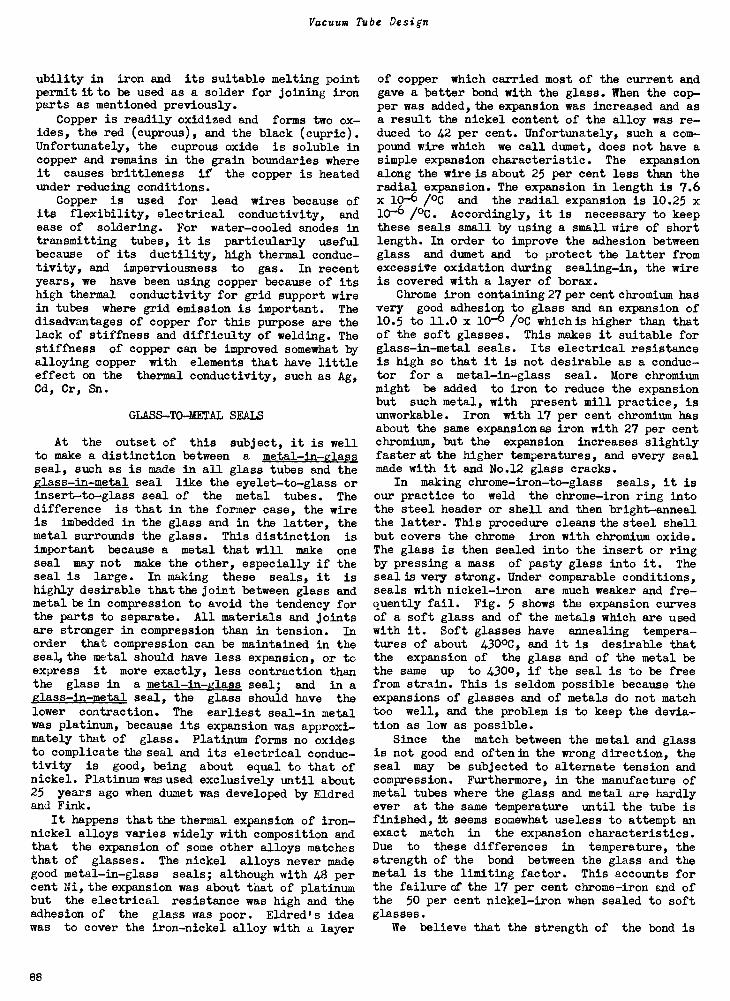
Vacuum Tube Design
ubility in iron and its suitable melting pointpermit it to be used as a solder for joining ironparts as mentioned previously.
Copper is readily oxidized and forms two ox-ides, the red (cuprous), and the black (cupric).Unfortunately, the cuprous oxide is soluble incopper and remains in the grain boundaries whereit causes brittleness if the copper is heatedunder reducing conditions.
Copper is used for lead wires because ofits flexibility, electrical conductivity, andease of soldering. For water-cooled anodes intransmitting tubes, it is particularly usefulbecause of its ductility, high thermal conduc-tivity, and imperviousness to gas. In recentyears, we have been using copper because of itshigh thermal conductivity for grid support wirein tubes where grid emission is important. Thedisadvantages of copper for this purpose are thelack of stiffness and difficulty of welding. Thestiffness of copper can be improved somewhat byalloying copper with elements that have littleeffect on the thermal conductivity, such as Ag,Cd, Cr, Sn.
GLASS -TO -METAL SEALS
At the outset of this subject, it is wellto make a distinction between a metal -in -glass
seal, such as is made in all glass tubes and theglass -in -metal seal like the eyelet -to -glass orinsert -to -glass seal of the metal tubes. Thedifference is that in the former case, the wireis imbedded in the glass and in the latter, themetal surrounds the glass. This distinction isimportant because a metal that will make oneseal may not make the other, especially if theseal is large. In making these seals, it ishighly desirable that the joint between glass andmetal be in compression to avoid the tendency forthe parts to separate. All materials and jointsare stronger in compression than in tension. Inorder that compression can be maintained in theseal, the metal should have less expansion, or toexpress it more exactly, less contraction thanthe glass in a metal -in -glass seal; and in aglass -in -metal seal, the glass should have thelower contraction. The earliest seal -in metalwas platinum, because its expansion was approxi-mately that of glass. Platinum forms no oxidesto complicate the seal and its electrical conduc-tivity is good, being about equal to that ofnickel. Platinum was used exclusively until about25 years ago when dumet was developed by Eldredand Fink.
It happens that the thermal expansion of iron -nickel alloys varies widely with composition andthat the expansion of some other alloys matchesthat of glasses. The nickel alloys never madegood metal -in -glass seals; although with 48 percent Ni, the expansion was about that of platinumbut the electrical resistance was high and theadhesion of the glass was poor. Eldred's ideawas to cover the iron -nickel alloy with a layer
of copper which carried most of the current andgave a better bond with the glass. When the cop-per was added, the expansion was increased and asa result the nickel content of the alloy was re-duced to 42 per cent. Unfortunately, such a com-pound wire which we call dumet, does not have asimple expansion characteristic. The expansionalong the wire is about 25 per cent less than theradial expansion. The expansion in length is 7.6x 10⁻⁶ /°C and the radial expansion is 10.25 x10⁻⁶ PC. Accordingly, it is necessary to keepthese seals small by using a small wire of shortlength. In order to improve the adhesion betweenglass and dumet and to protect the latter fromexcessive oxidation during sealing -in, the wireis covered with a layer of borax.
Chrome iron containing 27 per cent chromium hasvery good adhesio4 to glass and an expansion of10.5 to 11.0 x 10⁻⁶ /°C which is higher than thatof the soft glasses. This makes it suitable forglass -in -metal seals. Its electrical resistanceis high so that it is not desirable as a conduc-tor for a metal -in -glass seal. More chromiummight be added to iron to reduce the expansionbut such metal, with present mill practice, isunworkable. Iron with 17 per cent chromium hasabout the same expansion as iron with 27 per centchromium, but the expansion increases slightlyfaster at the higher temperatures, and every sealmade with it and No.12 glass cracks.
In making chrome -iron -to -glass seals, it isour practice to weld the chrome -iron ring intothe steel header or shell and then bright -annealthe latter. This procedure cleans the steel shellbut covers the chrome iron with chromium oxide.The glass is then sealed into the insert or ringby pressing a mass of pasty glass into it. Theseal is very strong. Under comparable conditions,seals with nickel -iron are much weaker and fre-quently fail. Fig. 5 shows the expansion curvesof a soft glass and of the metals which are usedwith it. Soft glasses have annealing tempera-tures of about 430°C, and it is desirable thatthe expansion of the glass and of the metal bethe same up to 4300, if the seal is to be freefrom strain. This is seldom possible because theexpansions of glasses and of metals do not matchtoo well, and the problem is to keep the devia-tion as low as possible.
Since the match between the metal and glassis not good and oftenin the wrong direction, theseal may be subjected to alternate tension andcompression. Furthermore, in the manufacture ofmetal tubes where the glass and metal are hardlyever at the same temperature until the tube isfinished, it seems somewhat useless to attempt anexact match in the expansion characteristics.Due to these differences in temperature, thestrength of the bond between the glass and themetal is the limiting factor. This accounts forthe failure of the 17 per cent chrome -iron and ofthe 50 per cent nickel -iron when sealed to softglasses.
We believe that the strength of the bond is
88
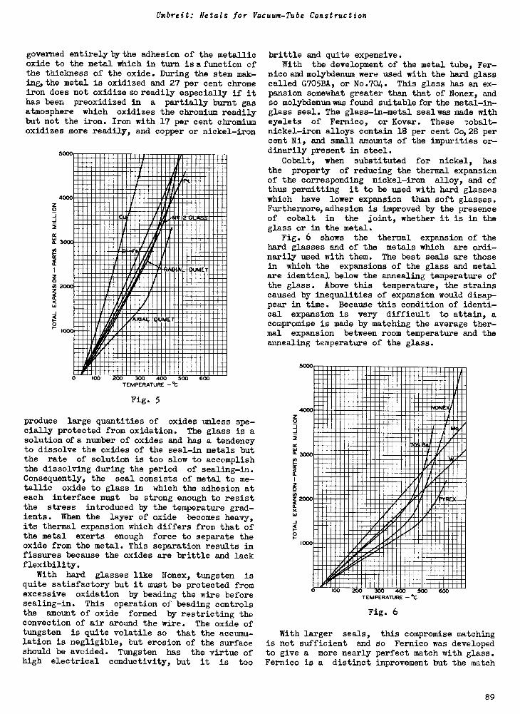
; - 11
:0 : :0 .34 : :0 - .11 I
6- 01: 11- : I 4
4- - 3. I I:
a d" 11- : - - : Z11-. Z
4: 11Z-11 :4
11: '11
1P I- 0:
:. Il '5:
: - 3
tt 11
lo- :
'11 11:
$ n-
".mmommommmmmmonmoommmommoommommammommmmamommammommonommainammoommmamu mmonammanommomammormammompaMENEMEMENEMEMMEMENNENAMMEMEME MMOMMENNEMEMMENNENC4UNNEMENS E NNMEMENEMMEMOMMENIUTMENM
mENNOMMMMMMMNMMMMWMOMEVRMUWMMMMMMU
mommommimmimmwmmommummoommammmommamoommw ammwommommwmuomommommemm
...mammon mmommonommmul/mmammommemmmmommommommommummammmonoommummummmmommommommommammmonnromnommmamonommE MMENNME =MOM NMEMPIEMOMMUMENNENMENNEN= MAME EMAIMPRIIMUIENEENMUM! SUMMUNNEWIAMMOMENOMMEMENNENNOMMINNE MUNE NIEMENANNUMME MBEN OMMEN= ONAMME nmromwmommommEmma
...mmmmommommwmmmm awinmnammomommomommmoommommommommanmummommmommommommammon maanwmuammommommommammamoommnom wammm4whommwmommummommmamommmm ummowouhniormmommmonnommme
.oM.nM.Mo.m.m.on..o.ru1m.ow..nmw.rrP.mMtoNmIommmutmrn4o,
I
N OENMENNEMPPANNEANW!Mil6W MOMmmmonommNommau4ilMUNMMOMMEM MEW".MMOMMENEEKIIM AEEONEE =MNN OEEENNDENCWAMMOMMONNMMEMEMMEMMMN OMMONWOWANEMPAINENTOMMEMENEMNN EMEMMOUUMPAMENME NOMENNOMMENMENEMOMMOUVAMENUMMEMEN MMEMEMMENN
fi 1
ammumwoowivAmmmnaammamm mmummmmummaMONMENOWINNE maw mommemmommimN OMMIMIWAMEgL L11.!11:1 EMENEMENOMMEMONNUEVOINMEN MOM NOMENNMEMONMEMMIPPIMMENNE EMENNMEMEMENNENNE
".MENNIUAMFOOMMELIMENEMMENEEMENNEMNommmur,orammmmmommommmamonnommommommommlrhyamomammommonommomammommommomomwaiwnwommonommmommommmmonmmommommanwqmnommommmomommommoonommommumE NEW4WEENNEMM MEMENMENMENEMENNEMU 4 NUMMUNINEMENTEIMAIMMIEMENNE EMONINEMMENEE NMMANN= MIMI MEMMUMMA= ONo rammomm mourn NOME MENNOMEMENO
. .. . ..
110 : : 0 0:
-
114
- .Z -
:0 41H 5: 04 Z
H
H.- 0 OZ 11:- 1 Z 111:
Z 0-
. - .6
4' : .0
d ;Z . : 1
-
Z 00 -0 0 4.
-4 Z "0-5 0- : - 41-
1: - 0:
HZ Z - 411 .4 -
1171 II - 1 : --$:
.1, : ": -. : :
-
43
4 11. :
: He
11-
Z .0
06: :46
11 - : :0
0- 111- :11
411
"-411 1 d-
It
:
:
4: -
11 6: O - -6
0: 414 14 0- : 11-.
et :P I - 11'0
04 Of 1
Z4 .0 - 6:
SO 9 4- 4-4
:1 Z-
- -4- Of
I
11
a- 5'
It
3
$' 0-,- 11-4 4- 11- : .Z
:45 11 :4 II - "0 : . : . -
3 z : : ; _
.3 f "11113' : : -: :$ 0 .-O HO 0014 0 ': 0 1 $ - :0 -
O Z : : - 11- : Z. .7.. t :0 1
3
1 , 11 : 4 : 6-
Z4 : 0 "HI ' d - I: 116
4 1-
6: - . :
96; -11 Z
d - Z 60441 1 I
- H
1:
11:
11:
11-4
a -
-
-
:6 -
. :
d- 0: - 0:
.0 S :00
4 0- --0 4 0 . - -
- 04 - 3 : ; --
ON - it 0,-0 0, R: 0 -1- '
:
a-
; 50 II:4'
..0- 11-
: 6-
'00,"
4-111 :
414
. -
-
3 1-
1 f": :
'HOZ I
- 6 - 6;4 64 '0 6 6 :0
I.: 0" :-
: ' 6.1 .0
41110 11 - - - 11 : :1 11 H1 4
0 0-
d' 5 Z
53 .-4 It :
- 1: :
".MENOMMEMEMEMENNEMENNOMMENOMMEMENENMEMMONIMEMENEUMENENNEMENEM MENEM=
MIMENNEEMEMENEMMEMENEMEMEM MEM,MMOMMMNMMMMMMMMMMNMMMMMMM =MEMNEENNOMMEMENNEEMEMEMENEN MEM=NOMMENE ONEENIIMENEMENNEMMO MENEMMOM= MEM MOMMUMME MENEMMONNIENNEEMEN MEMENNOMMENO.MOM
" MMENNEMMENNENEMENNEMENNIMMENMONMENNOMMEN MONEMMENNEEMONWEN
NOMMENNOMMEN EMENNEMENEEMMEMONEMENNEMONNEME EMMENNENNEMENUME,NEMEMOMMENNEN MEMONNEMME mmarmwmanniummumm mmwommonsmon RowanIIIIIII IIIIIIIIIIIIIIIIIII :rill
Immonemm mommummlimmibmn w ummommomm mmmommommo mamomrA mum.mmommom mommomom mwommma 'EMEMIPA" mmommommommomommommommmowsrmmarEMOMMEENNOMMENIMENNEMENNENMMEMMEMNON MONNE =NM MENU," MEgliMEM= MENNEN NOMME MEMO I MIMEMOM= NEEMENNEMONMMOU A NNEE NNEMENNENNEEN MMENEMAA
mmummirdwmuir. MA=MEM= MN= ISAMON, onmom= mom g morAmwaram w...mmommommonmonn mgmmuninsmMENEMENNEMEMEN MEMMEIAMANEVMENEMMINOMMEM MEMMUIFENIFMENNE =MEME MMEN MENEM FAINAM2Inel 1ms
16
MENNONEEMENUAMPAMI AA g MM =MINMENNOMMONNEWKII AMMONS MNMENEMMINOMMUMAMEAMMENNN OMMENNMENKM2=goWSMENEMENNOM
., NEMENNONOMMKIM . NEMMENEEMENmmommommormFame#2mmummummammummommmommmonar.arrelammmmimmommoomammmiN OMMEMENAC M CAW M NENNOMUMMENOMMEMEE MEMENOW% M T.02 MM IMMENIMENNEMEMENERw omman&ammommommmEmomommammomamminummmommemmmommmmismommomammnoslommommommmomillonommommommulpamowydnimmommagmon.mon mmmommommommo rdimmom mommonmonmmom IIIIImmmmiMONNE
4
:- 4
'4 :40
-1.
H Z U.
- 11
6- US
,ZIZ 0
6-0

Vacuum Tube Design
with glass is not exact and various heats ofFernico differ in expansion. The reason forthis is that small amounts of some impurities orslight variations in the major constituents havea large effect on the thermal expansion. Carbonhas the greatest effect and its amount is diffi-
cult to control because it is easily introducedor lost during heating operations. Variationsin annealing and amount of cold work have an ef-fect on the expansion of Fernico, but these arenot important except in large seals.
90

Lecture 9
GLASS AND ITS PROPERTIES
G. R. Shaw and C. A. Jacoby
DEFINITION
Various definitions of glass have been givenby different authorities but probably the mostlogical one for our purpose is by Littleton andMorey, who state that glass is an industrial ma-terial obtained by melting together various in-organic oxides (or compounds that yield oxidesby decomposition during the melting process) andcooling the resulting solution so that crystal-lization does not take place.
COMPOSITION
The various physical properties of glass aredetermined primarily by the chemical compositionof it. The glasses commonly used for radio tubesmay be divided generally into soft and hardglasses depending upon the temperature requiredfor working them.
In the soft -glass group, we have the soda -potash -lead glasses identified as No.1, No.12,and No.816 (814KW), together with the soda -limeglass identified as No.8. The soda -potash -leadglasses are used for tube stems where dumet leadwires are sealed into the glass stem press. Theymay also be used for chrome -iron seals, as inbutton stems. The soda -lime glass is used forbulbs of radio tubes which are sealed to lead -glass stems. This glass is also used for somespecial tubes, such as gas phototubes. In thiscase, it is used because it is not attacked bythe caesium.
In the hard -glass group, we have the lead -boro -
silicate glass No.772 (702P), and the boro-sili-cate glasses No.774 (726MX) and No.704 (705BA).The lead-borosilicate glass has the trade nameNonex and is used for tube stems where tungstenlead wires are sealed into the glass stem press.It is also used for bulbs. The borosilicateglass 774 (726MX) is a chemical -resistant glassand has the trade name Pyrex. It is used fortransmitting and cathode-ray tube bulbs. The 704(705BA) glass is used with Fernico metal sealsand molybdenum lead -wire seals in metal tubes.
All of these glasses contain, and have as theirbase, silica which is obtained from sand. Theamount ranges from 57 to 72 per cent in the softglasses and from 72 to 81 per cent in the hardglasses. Another important constituent commonto all the glasses is sodium oxide. The amountranges from 3 to 4 per cent in the No.816 glassand is about 17 per cent in the No.8 glass. Ofall the constituents customarily present in glass,sodium oxide is the one which does most to de-crease the resistance of the glass.
All of these glasses contain some potassiumoxide. The amount ranges from that present asan impurity to 10 per cent in some of the soda-
potash -lead glasses. It serves approximately thesame purpose as sodium oxide in respect to lower-ing the viscosity and raising the coefficient ofexpansion, but gives a substantially higher re-sistance than does an equivalent amount of sodiumoxide.
The hard glasses are essentially borosilicates.Pyrex contains about 81 per cent of Si02 and some-what over 10 per cent of B203. This compositionserves as the base for the rest of the series,each one being suitably modified to accomplishthe purposes for which it is intended. Nonex,for example, has a percentage of the silica re-placed by lead oxide and the result is a glassin which the resistance is much improved, eventhough the viscosity range is lowered somewhat.
In general, the chemical compositions of thedifferent glasses may be represented by the fol-lowing equations, where x, y, and z are variablepercentages of the various constituents.
Lead Glasses
x Si02 + y Pb0 + z Na20 +
Lime Glasses
x Si02 + y Ca0 + z Na20 +
Borosilicate Glasses
x Si02 + y B203 + z Na20 +
CONSTITUTION
Recent speculations on the constitution ofglass based on x -ray evidence and studies of glassby means of x-rays indicate that the glassy stateis distinguished by a continuous, randomly ori-ented network of atoms. Picture diagrams of soda -silica glass aqd lead -oxide -silica glass areshown in Figs. 1' and 22, respectively.
PRODUCTION OF GLASS PARTS
Lime -glass bulbs in large quantities are pro-duced largely on the Corning, continuous -ribbon -type, bulb -blowing machine. Glass flows from amelting tank to a forehearth, thence through a
1 B. E. Warren and A. D. Loring, "X-ray Diffrac-tion Study of the Structure of Soda -Silica Glass,"
Jour. Amer. Ceramic Soc., Vol. 18, No.9, p. 275;1935.
2 George J. Bair, "The Constitution of Lead -
Oxide Silica Glass,"I. Atomic Arrangement, Jour.Amer. Ceramic Soc., Vol.19,No.12, p. 346; 1936.
91
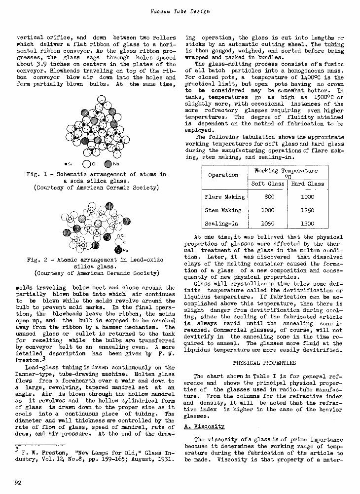
Vacuum Tube Design
vertical orifice, and down between two rollerswhich deliver a flat ribbon of glass to a hori-zontal ribbon conveyor. As the glass ribbon pro-gresses, the glass sags through holes spacedabout 3.9 inches on centers in the plates of theconveyor. Blowheads traveling on top of the rib-bon conveyor blow air down into the holes andform partially blown bulbs. At the same time,
Fig. 1 - Schematic arrangement of atoms ina soda silica glass.
(Courtesy of American Ceramic Society)
Fig. 2 - Atomic arrangement in lead-oxidesilica glass.
(Courtesy of American Ceramic Society)
molds traveling below meet and close around thepartially blown bulbs into which air continuesto be blown while the molds revolve around thebulb to prevent mold marks. In the final opera-tion, the blowheads leave the ribbon, the moldsopen up, and the bulb is exposed to be crackedaway from the ribbon by a hammer mechanism. Theunused glass or cullet is returned to the tankfor remelting while the bulbs are transferredby conveyor belt to an annealing oven. A moredetailed description has been given by F. W.Preston.3
Lead-glass tubing is drawn continuously on theDanner-type, tube-drawing machine. Molten glassflows from a forehearth over a weir and down toa large, revolving, tapered mandrel set at anangle. Air is blown through the hollow mandrelas it revolves and the hollow cylindrical formof glass is drawn down to the proper size as itcools into a continuous piece of tubing. Thediameter and wall thickness are controlled by therate of flow of glass, speed of mandrel, rate ofdraw, and air pressure. At the end of the draw -
3F. W. Preston, "New Lamps for Old," Glass In-
dustry, Vol. J2, No.8, pp. 159-165; August, 1931.
ing operation, the glass is cut into lengths orsticks by an automatic cutting wheel. The tubingis then gauged, weighed, and sorted before beingwrapped and packed in bundles.
The glass-melting process consists of a fusionof all batch particles into a homogeneous mass.For closed pots, a temperature of 1400°C is thepractical limit, but open pots having no crownto be considered may be somewhat hotter. Intanks, temperatures go as high as 1500°C orslightly more, with occasional instances of themore refractory glasses requiring even highertemperatures. The degree of fluidity attainedis dependent on the method of fabrication to beemployed.
The following tabulation shows the approximateworking temperatures for soft glass and hard glassduring the manufacturing operations of flare mak-ing, stem making, and sealing-in.
OperationWorking Temperature
oc
Soft Glass Hard Glass
Flare Making
Stem Making
Sealing-In
800
1000
1050
1000
1250
1300
At one time, it was believed that the physicalproperties of glasses were affected by the ther-mal treatment of the glass in the molten condi-tion. Later, it was discovered that dissolvedclays of the melting container caused the forma-tion of a glass of a new composition and conse-quently of new physical properties.
Glass will crystallize in time below some def-inite temperature called the devitrification orliquidus temperature. If fabrication can be ac-complished above this temperature, then there isslight danger from devitrification during cool-ing, since the cooling of the fabricated articleis always rapid until the annealing zone isreached. Commercial glasses, of course, will notdevitrify in the annealing zone in the time re-quired to anneal. The glasses more fluid at theliquidus temperature are more easily devitrified.
PHYSICAL PROPERTIES
The chart shown in Table I is for general ref-erence and shows the principal physical proper-ties of the glasses used in radio-tube manufac-ture. From the columns for the refractive indexand density, it will be noted that the refrac-tive index is higher in the case of the heavierglasses.
A. Viscosity
The viscosity of a glass is of prime importancebecause it determines the working range of temp-erature during the fabrication of the article tobe made. Viscosity is that property of a mater -
92
Shaw and Jacoby: Glass and Its Properties
a)
,-I+) Xoit.) 'ci
04)4 Hi-Ia)c0
CV
Lc-,
H
CV
U -N
H
NtilH
enInV \
H
-4N-3H
N03
H
000
H
r -sa)
c.) 0old `0or0 ,0 trs-I o ca(/) ODa) CD
C4
0OsHH
\ 0Ca
01
00asHH
00cn\ 0CO
cs'N\ 0csi
0NHH
00COIS \
CD0$4 430 0 0
-1 00 -1 crg:21154Rtic,a) 0
0(3
NLH
0as
r:
asas
r-
NtO
.7.
asas
=
CaCO
:::.
\C)CO
:-.
sr).4
4 +3
+, .CO Pi
co .4 co CO C% -4 -4
to.4+30 ,-1 0
0404 ,i
Incr,-4
c....,-4
....,in ctin .3
OD
4-1ta.40CO
1).
.1-1 )11CO 0
Sti)
r)
kr\toCa
N-4Ca
-4-0cn
asOs
Ca
Cr%Ca
Ca
IAcfN
ca
401
0)CO
40
.4430
+)r.
S ..0
.$ Hco 10
ta0 tx0
.r0 .00 0+) +)
0)S S .0
4)) -4()) HCl) Cl) cri
1:0)
.4ga0
4)tsa)
CO
.1-1 0ii 0
lco '44ant
CO
a)
0 A10 09
.-,11,1
a) 0.-1 Ari
' 9e.,0=
'40=
vim)
0H0
H tO
r-10
(0
r--- ..---. N.".- 1X) N 00o
`.vCNI 0N N
0N..-..4If0\N
ial or mixture which resists flowing when a forceis exerted upon it. The unit of viscosity is thepoise. It is defined as the force exerted tan-gentially on one square centimeter of either oftwo horizontal planes one centimeter apart, whichwill move the one plane at the rate of 1 cm/sec.with reference to the other, the space betweenthe two planes being filled with the viscousliquid. Expressing this definition by an equa-tion, we have
P =VA
where,p = viscosity in poisesF = force in dynesA = surface in sq.cm.V = velocity in cm/sec.
1)_Fabrication -- At the fabrication point,or the time when the glass is drawn from the potor tank, its viscosity should be 105 poises. Forpurposes of comparison, the viscosities of someother substances at room temperature are:
Substance ViscosityPoises
Water 0.01
Glycerine 10
Glucose 1000
2)Softening Point -- Glass has no definitemelting point but the softening point of allglasses is designated in this country as thetemperature corresponding to adefinite viscosityof 4.5 x 10⁷ poises. As a check on the manufac-turing operations in the glass works, the follow-ing test has been installed. The softening pointis determined as that temperature in degreesCentigrade at which a glass fiber (diam. = 0.55to 0.75 ram± 0.01mm; length = 23.5 cm) will elon-gate under its own weight in a special furnaceat the rate of 1 mm/min. Commercial variationspermitted in the value of this constant are: ± 5°Cfor glasses having a coefficient of expansion per°C above 50 x 10-7, and ± 10°C for glasses below50 x 10-7.
3) Annealing_Point --The annealing pointis designated as that temperature correspondingto a viscosity of 2.5 x 10¹³ poises. It is alsodefined as the temperature at which 90 per centof the strain in the glass is removed in 15 min-utes in a glass sample 1/4 inch in thickness.This temperature is sometimes called the upperannealing temperature.
4) Strain_ Point -- The strain point is
designated as that temperature corresponding toa viscosity of 4.0 x 10¹⁴ poises. It is also de-fined as the temperature at which 90 per cent ofthe strain is removed in 4 hours in a glass sam-
93
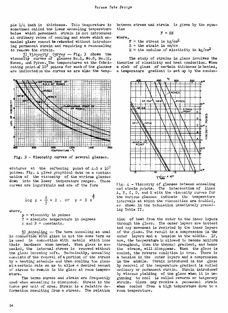
Vacuum Tube Design
ple 1/4 inch in thickness. This temperature issometimes called the lower annealing temperaturebelow which permanent strain is not introducedat ordinary rates of cooling and above which an-nealed glass cannot be reheated without introduc-ing permanent strain and requiring a reannealingto remove the strain.
5)Viscosity_Curves -- Fig. 3 shows the
viscosity curves of glasses No.1, No.8, No.12,Nonex, and Pyrex. The temperatures at the fabri-cating point of 105 poises for each of the glassesare indicated on the curves as are also the temp -
6
7
6
47)oUS
t 4
03
AN,00.641040-0 6 POI SES
POIIFT
..h,..,4 wh....,..1molobr__mb.
m1om
111
im smasminnink....umm....m wommags. MOMOIOMMEM\fl
11 MI& -.MillipbbMN .1. MilsMEME "111111 -MO
600 800 1000 1200TEMPERATURE -°C
1400 1600
Fig. 3 - Viscosity curves of several glasses.
eratures at the softening point of 4.5 x 10⁷poises. Fig. 4 gives graphical data on a contin-uation of the viscosity of the various glassesdown into the lower temperature ranges. Thesecurves are logarithmic and are of the form
log p =-A
+ B , or
A
p = Be T
where,p = viscosity in poisesT = absolute temperature in degreesA and B = constants.
6) Annealing. --The term annealing as usedin connection with glass is not the same term asis used in connection with metals which losetheir hardness when heated. When glass is an-nealed, the internal stress is removed withoutthe glass becoming soft. Technically, annealingconsists of the removal of a portion of the stressby a heating schedule and then cooling the glassat acertain rate so as to allow a desired amountof stress to remain in the glass at room temper-ature.
The terms stress and strain are frequentlyused when annealing is discussed. Stress is theforce per unit of area. Strain is a relative de-formation resulting from a stress. The relation
between stress and strain is given by the equa-tion
where,F =S =E =
F = SE
the stress in kg/cm2the strain in cm/cmthe modulus of elasticity in kg/cm2
The study of strains in glass involves thetheories of elasticity and heat conduction. Whena slab of glass of certain thickness is heated,a temperature gradient is set up by the conduc-
2
N21
N2 704
N212
-ANNEALINGPOINT
°C4 5
N*8
NONEX
PYREX
so
STRA N/POINT E
8
A
IS 4X10⁴io4
T AB&
Fig. 4 - Viscosity of glasses between annealingand strain points. The intersection of linesA, B, C, D, and E with the viscosity curves forthe various glasses indicate the temperatureintervals at which the viscosities are doubled,as shown in the tabulation immediately preced-ing Table II.
10
o8
2.4
1016
1012
tion of heat from the outer to the inner layersthrough the glass. The outer layers are hottestand any movement is resisted by the inner layersof the glass. The result is a compression in theouter layers and a tension in the middle. If,
now, the temperature is allowed to become uniformthroughout, then the thermal gradient, and hencethe stress, will disappear. When the glass iscooled, the reverse condition is true. There isa tension in the outer layers and a compressionin the middle. Strain introduced in the glass
by removal of the temperature gradient is calledordinary or permanent strain. Strain introducedby viscous yielding of the glass when it is be-ginning to cool is called reverse or temporarystrain. Glass may receive a permanent strain
when cooled from a high temperature down to aroom temperature.
94
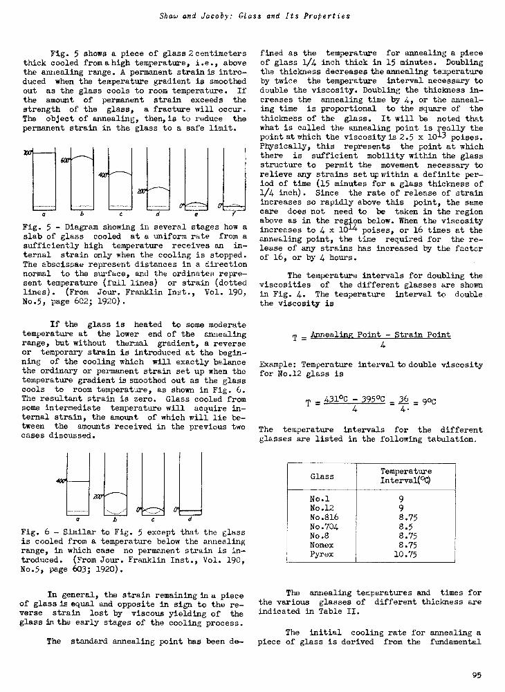
Shaw and Jacoby: Glass and Its Properties
Fig. 5 shows a piece of glass 2centimetersthick cooled fromahigh temperature, i.e., abovethe annealing range. A permanent strain is intro-duced when the temperature gradient is smoothedout as the glass cools to room temperature. Ifthe amount of permanent strain exceeds thestrength of the glass, a fracture will occur.The object of annealing, then, is to reduce thepermanent strain in the glass to a safe limit.
:1"-U4ciM,Fig. 5 - Diagram showing in several stages how aslab of glass cooled at a uniform rate from asufficiently high temperature receives an in-ternal strain only when the cooling is stopped.The abscissae represent distances in a directionnormal to the surface, and the ordinates repre-sent temperature (full lines) or strain (dottedlines). (From Jour. Franklin Inst., Vol. 190,No.5, page 602; 1920).
If the glass is heated to some moderatetemperature at the lower end of the annealingrange, but without thermal gradient, a reverseor temporary strain is introduced at the begin-ning of the cooling which will exactly balancethe ordinary or permanent strain set up when thetemperature gradient is smoothed out as the glasscools to room temperature, as shown in Fig. 6.The resultant strain is zero. Glass cooled fromsome intermediate temperature will acquire in-ternal strain, the amount of which will lie be-tween the amounts received in the previous twocases discussed.
Fig. 6 - Similar to Fig. 5 except that the glassis cooled from a temperature below the annealingrange, in which case no permanent strain is in-troduced. (From Jour. Franklin Inst., Vol. 190,No.5, page 603; 1920).
In general, the strain remaining in a pieceof glass is equal and opposite in sign to the re-verse strain lost by viscous yielding of theglass in the early stages of the cooling process.
The standard annealing point has been de-
fined as the temperature for annealing a pieceof glass 1/4 inch thick in 15 minutes. Doublingthe thickness decreases the annealing temperatureby twice the temperature interval necessary todouble the viscosity. Doubling the thickness in-creases the annealing time by 4, or the anneal-ing time is proportional to the square of the
thicknets of the glass. It will be noted thatwhat is called the annealing point is really thepoint at which the viscosity is 2.5 x 10¹³ poises.Physically, this represents the point at whichthere is sufficient mobility within the glassstructure to permit the movement necessary torelieve any strains set up within a definite per-iod of time (15 minutes for a glass thickness of1/4 inch). Since the rate of release of strainincreases so rapidly above this point, the samecare does not need to be taken in the regionabove as in the region below. When the viscosityincreases to 4 x 10¹⁴ poises, or 16 times at theannealing point, the time required for the re-lease of any strains has increased by the factorof 16, or by 4 hours.
The temperature intervals for doubling theviscosities of the different glasses are shownin Fig. 4. The temperature interval to doublethe viscosity is
T Annealing Point - Strain Point
4
Example: Temperature interval to double viscosityfor No.12 glass is
T = 431°C - 395°C 36 9°C4 4- -
The temperature intervals for the differentglasses are listed in the following tabulation.
GlassTemperatureInterval(°C)
No.1 9No.12 9No.816 8.75No.704 8.5No.8 8.75Nonex 8.75Pyrex 10.75
The annealing temperatures and times forthe various glasses of different thickness areindicated in Table II.
The initial cooling rate for annealing apiece of glass is derived from the fundamental
95
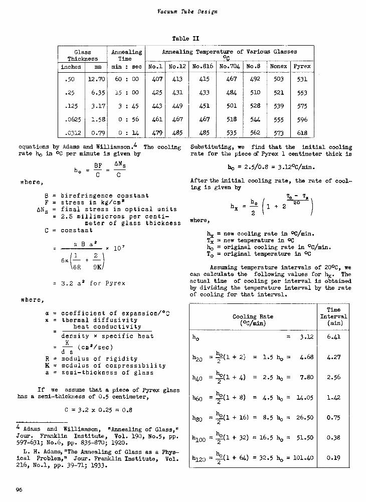
Vacuum Tube Design
Table II
GlassThickness
AnnealingTime
min : sec
Annealing Temperature of Various Glasses°C
inches mm No.1 No.12 No.816 No.704 No.8 Nonex Pyrex
.50 12.70 60 : 00 407 413 415 467 492 503 531
.25 6.35 15 : 00 425 431 433 484 510 521 553
.125 3.17 3 : 45 443 449 451 501 528 539 575
.0625 1.58 0 : 56 461 467 467 518 544 555 596
.0312 0.79 0 : 14 479 485 485 535 562 573 618
equations by Adams and Williamson.4 The cooling Substituting, we find that the initial coolingrate ho in 00 per minute is given by
h."
where,
BF
C
ANs
C
B = birefringence constantF = stress in kg/cm2
pNs = final stress in optical units2.5 millimicrons per centi-
meter of glass thicknessC = constant
where,
B a'x 10'
6x(1 2-- +6R 9K
= 3.2 a2 for Pyrex
a = coefficient of expansion/°Cx = thermal diffusivity
heat conductivity
R =K =a =
density x specific heatK
(cm2/sec)d s
modulus of rigiditymodulus of compressibilitysemi -thickness of glass
If we assume that a piece of Pyrex glasshas a semi -thickness of 0.5 centimeter,
C = 3.2 x 0.25 = 0.8
4 Adams and Williamson, "Annealing of Glass,"Jour. Franklin Institute, Vol. 190, No.5, pp.597-631; No.6, pp. 835-870; 1920.
L. H. Adams,"The Annealing of Glass as a Phys-ical Problem," Jour. Franklin Institute, Vol.216, No.1, pp. 39-71; 1933.
rate for the piece of Pyrex 1 centimeter thick is
ho = 2.5/0.8 = 3.12°C/min.
After the initial cooling rate, the rate ofing is given by
To - T,
hX = - (1 + 220 )ho
2where,
cool-
hx new cooling rate in 0C/min.Tx = new temperature in 0Cho = original cooling rate in °C/min.To = original temperature in 0C
Assuming temperature intervals of 20°C, wecan calculate the following values for 4x. Theactual time of cooling per interval is obtainedby dividing the temperature interval by the rateof cooling for that interval.
Cooling Rate(°C/min)
TimeInterval
(min)
110 = 3.12 6.41
h20 = y(1 + 2) = 1.5 ho = 4.68 4.27
h40 = Lf.(1 + 4) = 2.5 ho = 7.80 2.56
h60 = 1;7°41 + 8) = 4.5 ho = 14.05 1.42
h80 = 1.2.(1
2+ 16) = 8.5 ho = 26.50 0.75
h100 = 34°'.(1 + 32) = 16.5 110 = 51.50 0.38
h120 = 112.(12
+ 64) = 32.5 110 = 101.40 0.19
96
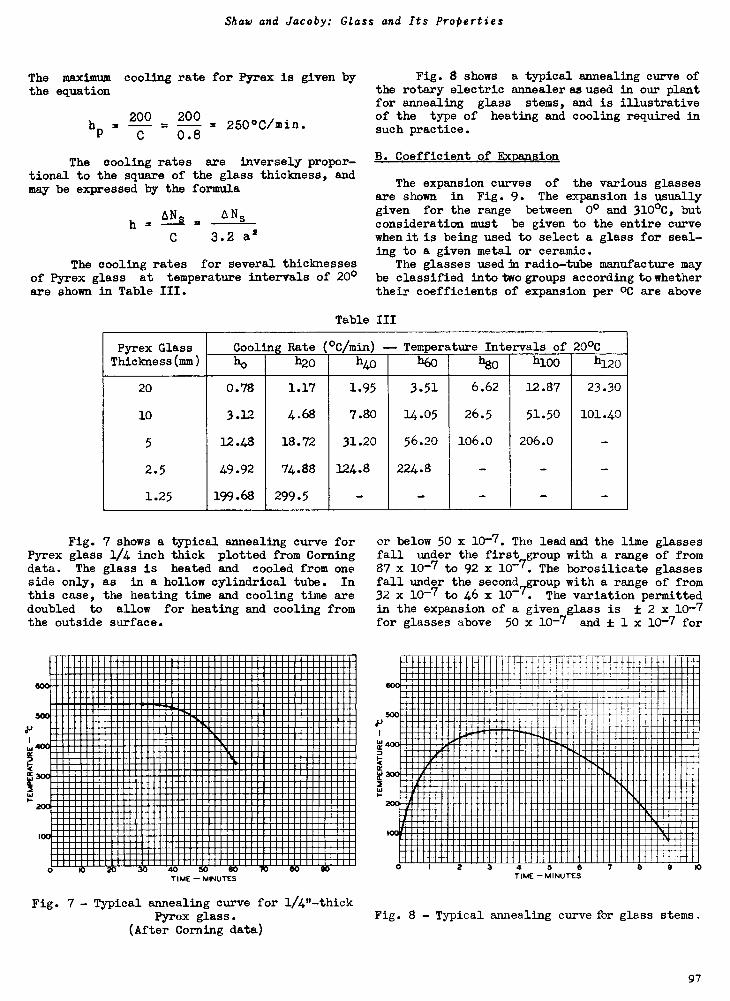
Iti Z
99a
0
0: SIP Z- _S 0
. d: -0 : 40" - :11$
0: Z. -I 09
0-
- - - -
- 0 ; -
: Z
- 3 - -
a
Z 011
A
. 0 - O
a
ho
- 0 : : .0
h20
:* Cu
OO Z.
00 0-
: 0-
:CO *0 I:
.0
-: Z ." .:0
:0
0:
. N 4: - .4- 4:0:
Oil 11
- . -
8- -
a- - -
& 0 I
-0 4
4: . 0
0.11- :.: - I
- . --. "s 11
Z : ." Z - II S - II:
s- : - S. 0- . IP
4- - :4 - 0: - fill "
1140
II 0
; -
0
E MEMMEMEMESSIMMENIIMMUS EEEEEEEEEE UMMENNEMMUSSI MMMMMMMMISSERSEMMEMEMMEMS MMMMMMMMMMMMM 111111111111111111MMII MMMMMM MMMMM MOISMONOMMON MMMMMMMMMMMMMM MMMMMMMMM MMMMM
"mom MMMMMMMMMM mammon MMMMMMMMMMMMMMMMMMMMMMM memmmmommnses MMMMM moms MMMMMMMMMMMMMMMMM mommmommmmm
ossem MMMMMMM mum MMMMM n' mommemmommmmammommomm MMMMMM mum MMMMMM ammmommonsmoneIMMENNOSIIMMEMEMEMEMEMEM MMMMMMMMMMMMMM MMEMISENNEWIIME
MMMMMMMM MEM MMMMMMMMMMM MESSIESSIMMUNIIMMENSEMMEMOIS MMMMMMM MMMMM MEMENNEWILMEN MMMMMMMM MEMMONSIMMEM
"mmamm MMMMMMMMM mommann MMMMMMMMMM amemmammn MMMMMMM nommom MMMMM mmosnmem MMMMMMMMMMMM o MMMMMMMMMMMM mmommemm
UMM MMMMM MMMMMMM MEM MMMMMMMMMM MMUS MMMMMMMMM MEN11111111
"emm MMMMMM mum MMMMMMMMMMMMM MMMMM mmammommemnammmmmemmmoms MMMMMMMMM mem MMMMMM memmommommmon
"an MMMMM mom MMMMMMMM mon MMMMM mommonsmammommmmommmnamemommommemn MMMMM nommmommmsnmemmommommammommommemommammo MMMMMM masonanammosammemmm MMMMMMMMMMMM m MMMMM mommemmosnmommmannommommmom MMMMMMMMMMMMM somommmamamm
ammomommmommnamommanemanmennommen"mannommonammommanna MMMMMMMMMM m MMMMM omens MMMMMMM memam MMMMM m MMMMMMMMM MMMMM MIIMMESEMENUMMEMMEMMEMEMEMM
MMMMM a MMMMMMMMM MMUMMEMENES MMMMMMMMM IIMMMOMMEMEM
...4ENSISAMMICIAMMEVAINEKI111111BAIMM[IsMEMC..
$
-00: .
1160 h80 h100
I I 9 9
s- ''
Ss"8
1.
e
4- -
:
h120
-: .01/ I -
:Z1-
:
;
-
Z
0. It
:16
Ofl
-
MMMOMMIMMOMMOMMMOMmIlifiMIMOIMMOMIMMOMMOOmOm Ma IIIIIIIIIMMEMOMMOOMMMMINIMMIMIMMIMM MMMMM OM SW MENUMENIIMMIS
MMOMMOMMEMMEMMEMEMMOMMON mmommammm. MMMMMmon sum m m pg 1agummumm ..ow MMMMM immismissummum um s Es ftmu MMMMM mum. emnammammnammammm mmm moms mpmemmommnammommmmemmenemmommimilmmommommmm
m MMMMM ammoommagnmmmommmommmommummmi mmmummmmmenmemmmemmwE ..mmummonnemmaam En magmemmmmmemmommommdamommennamgnemmmmmmonmm anommemmemmmil
..m MMMMM Meng allIACIIMMEMEMEMMENEBEIMMEMEMME
1
MEGMNIIIKAMEMENOMMISINIMMENSIOSMEMMEMMEMME SIMMENNESAMEMMEMEMIAMMEMISEMMEMENZUMMISEMEN OEM"M MEMBEEME
momenommennommmmemmoommmmammmmgiammmommm ammmommmmmormommemmmommmammmommommnammom MM s MM nmmommammommn
"mmosammammummommmommmommmmommmosommonommmennammangmerneemmmommmommummmnammenammommommommommammammmmanummummummommonamommmmommmommommemmommonnammanne
iTm MMMMM mmammmommomsommmomm MM o MM mmommumma..mmmsonmennamomm MMMMMMMMMMMMMMMMMMM o mammaimmune monammummmmommenomme MMMMM OMMIOMOMMEMMUMMEIIIIMINMEM monnmemmommmummommmommommmmammommmmanmeI monnomnmnammmommommemmminemem MMMMMM mom=nomomme mommommommommummessummissmomm
, 41121INEWOMMOMMEMIMMEMENSIIMMEMEN MMMMM MEMEMMENWOMMUNG.1111111IMMESEEM MMMMMM MISSEEMMEMEMEMMOMMOMMEMOMMEMOSSISENE MMEMISMISOMMUMMOMMMEMMEME MMMMM ISMOMMEMENUMEMEMMOOMMMEMEMEMENN MMMMMMMMMMMMMM MIMS MMMMMMMMMMMMMMMM ssiESMEMENNUME MMMMMMMM EMOMMOMMENUMMEMOMMMOMMEMMEMEMEMEMMIME
: - II

Vacuum Tube Design
glasses below 50 x 10-7.In the design of glass -metal seals, the selec-
tion of the proper glass to match the metal de-pends aithe type of seal to be made. In general,it is important to remember that the glass shouldalways be left ina state of compression when the
4
3
0
1_1111111111111 'I
=ANNEALING POINT(sEt FIG.))
TEMPERATURE -
PY
Fig. 9 - Expansion curves of variousglasses.
seal is cooled down to room temperature, providedthe safe compressive strength is not exceededwhich might cause a failure of the glass seal.The points marked on the expansion curves inFig. 9 are the standard annealing points givenin Table I.
C. Thermal Endurance of Glass
Thermal endurance is that property of glass bywhich it can withstand sudden changes of temper-ature without breaking. Denoting this propertyby F, we have
F =a E d s
where,
P = tensile and compressivestrength in kg/cm2
a = coefficient of expansion/°CE = elastic coefficient (Young's
modulus) in kg/cm2K = thermal conductivity
in cal/cm/°C/sec.K
ds= thermal diffusivity in cm2/sec.
Each of these factors will now be discussed.
1) TensileandCompressive Strength -- Whenstresses exceed the tensile or the compressivestrength of the glass, fracture will occur. Whensudden cooling takes place, the tension in thesurface layers is the greater stress. Suddenheating causes a high surface compression. Thesafety of glass depends upon its tensile strengthbecause the compressive strength of glass is al-ways greater than the tensile strength. It isevident that glass will more readily withstandsudden heating than sudden cooling. Values fortensile strength and compression strength arenot well coordinated, but for purposes of anyordinary calculations, the following values maybe used.
GlassTensile Strength Compressive Strength
lbs./in.2 k c2 lbs./in.2 kg/cm2
Hard
Soft
10000 700
6000 420
170000 1200
114000 800
An inspection of the figures shows immediatelywhy compressive strains are more desirable thantensional strains.
2) Coefficient of Expansion -- Sudden cool -ingof glass causes the surface layers to rapidlycontract and throws them into a state of tension,while at the same time the interior is throwninto a state of compression as previously out-lined. The reverse is true when the glass issuddenly heated. This action is best explainedby the fact that any movement of the outer lay-ers is resisted by the inner layers of the glass.Consequently, there exists a neutral zone wherethere is zero stress between the inner and outerlayers during heating or cooling. The greaterthe rate of thermal expansion or contraction, themore intensely will glass be stressed. Glasseswith relatively low thermal expansion will showthe highest thermal endurance. The thermal en-durance of the various glasses is inversely pro-portional to their coefficients of expansion byactual test and is so indicated in the aboveformula.
3) Elastic Coefficient(Youn&_Modulus) --Low elasticity favors thermal endurance sincethe stress set up by local strains will be lessthan in glass with a high elastic coefficient.Values for elasticity are as follows:
Elastic CoefficientGlass
lbs/in.2 x 10-6 kg/cm2 x 10-6
Hard 9.23 0.650
Soft 8.88 0.625
98
Shaw and Jacoby: Glass and Its Properties
4) Thermal Conductivity - High thermal con-ductivity favors thermal endurance since heatsuddenly applied locally is rapidly transferredthrough the glass and stresses due to unequalexpansion are minimized.
5)Thermal Diffusivity -- Thermal diffusiv-ity denotes the rate at which the interior of theglass is heated or cooled from the outside. It
depends on the thermal conductivity (K), thedensity (d), and the specific heat (s).
The thermal endurance depends upon thesquare root of the diffusivity. A glass havingfour times the diffusivity of another glass willconsequently have twice the thermal endurance ofthe other glass. The higher the diffusivity, thehigher the thermal endurance, everything else be-ing equal.
A list showing the thermal endurance of thevarious glasses in percentage of that of Pyrexis given below:
GlassThermal Endurance
Pyrex 100.0Nonex 89.5
No.705 BA 71.7No.8 27.7No.12 20.6No.1 20.5
No.814 KW 19.3
D. Weathering
One of the sources of failure of glass is theweathering which occurs in the case of exposureto the atmosphere. The atmosphere always con-tains moisture and gases, such as carbon dioxide.In cities, small amounts of ammonia, sulpherettedhydrogen, and sulpherous and sulphuric acids arealso usually present in the atmosphere. Aftermore or less prolonged exposure to the atmosphere,the surface of window and similar types of glassis roughened and becomes coated with an irides-cent or opalescent coating. With optical glass,atmospheric weathering is of extremely great im-portance. The formation of a slight film onlenses is often disastrous in its results on ex-pensive and delicate optical combinations. Thematter is further complicated by the fact thatglass of relatively poor chemical stability hasto be used sometimes in order to obtain otherdesired properties.
The nature of weathering and chemical attackis worth considering. Moisture in contact withglass is first of all adsorbed and then absorbed.The resulting hydration is succeeded by the hy-drolysis of the soluble silicates forming partof the complex silicate mixture of which glassconsists. In a soda -lime glass, such as No.8lime -glass bulbs, sodium metasilicate is the mostsoluble silicate present and hydrolysis chieflyresults in the liberation of sodium hydroxide andsilicic acid according to the equation:
Na2SiO3 + (x + 2) H2O = H2SiO3 xH20 + 2NaOH
The caustic soda passes into solution while thesilicic acid (which contains an uncertain numberof molecules of water of hydration) is also tosome extent soluble, and again is partly mechan-ically removed, often giving the water a turbidappearance. The action of the water is not al-ways on the surface, for it can be shown that inmany cases the water penetrates to an appreciabledepth below the surface, which, on subsequentheating and drying, shows a large number of mi-nute cracks giving the glass a dull appearance.
The attack of a moist atmosphere upon glassresults in the absorption of appreciable amountsof water, and it is found that glasses best re-sisting the attack of water condense the leastmoisture upon their surfaces. The condensed wa-ter attacks the glass, breaks down the silicates,and leaves a solution of caustic alkali on thesurface of the glass as previously explained.When the air contains carbon dioxide, a furtherreaction occurs between the gas and the alkali,and results in the formation of a carbonate. In
the case of soda glasses, sodium carbonate willresult according to the equation:
2NaOH + CO2 = Na2CO3 + H2O
The sodium carbonate so produced, when appreci-able attack occurs, crystallizes out in fine nee-dles upon the surface and the white deposit re-sults in the dimming of the glass. By rubbingoff the crystals with a dry cloth, the surfaceof the glass may be badly scratched, but the de-posit can be removed without damage by washingwith water. Washing, however, will not removethe surface layer of silica obtained by the hy-drolysis, so that a filmed glass surface cannever be satisfactorily cleaned with water alone.
Atmospheric attack on potash glasses resultsin the formation of potassium carbonate, a sub-stance so deliquescent that it does not crystal-
lize out, but leaves amoist, greasy deposit uponthe glass when the surface is badly attacked.The attack of moist air on alkali -silicate glassis intensified by heating and effects have beenmade visible in 12 hours at 80°C in a moist at-mosphere. Glasses high in lead -oxide or barium -
oxide content are susceptible to attack by acidvapors in moist atmospheres and show filming anddulling of the surface.
ELECTRICAL PROPERTIES
A. Electrical Resistance
The resistance of the various glasses is shownin Fig. 10. It will be noted that the resistanceof No.8 lime glass is very low in comparison withthe resistances of the other glasses, in fact, itis only about 5 per cent of the resistance ofPyrex at a temperature of 250°C.
99
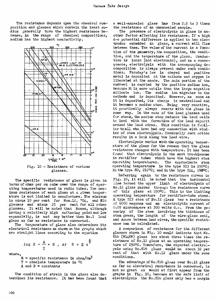
Vacuum Tube Design
P
The resistance depends upon the chemical com-position and glasses which contain the least so-dium generally have the highest resistance be-cause, in the range of chemical compositions,sodium has the highest conductivity.
4C
N912
O2 9 50
N2 12 ELECTROLYSIS,-UPPER LIMIT OF
X
8I6
NONE
N2
YRE
to,'
to*
a
102CO
U. 2
Ucc
a-
402
N 28
N22 21 20 19 18
X 104T ABS.
17 16
to7
10615
Fig. 10 - Resistance of variousglasses.
The specific resistance of glass is given interms of ohms per cm cube over the range of oper-ating temperatures used in radio tubes. The max-imum resistance of each glass at a given temper-ature is not limited in manufacture. The minimumis minus 10 per cent for Nos.12, 704, and 816glasses and minus 25 per cent for all otherglasses. It will be noted that Nonex, althoughhaving a relatively high softening point and lowexpansivity, is not any better than No.1 leadglass as far as resistance is concerned.
The temperature of glass also determines itselectrical resistance as shown on the graphs whichare straight lines according to the equation
log R = A + B , or R= BT
AT
where,R = specific resistance in ohms/cm3T = absolute temperature in OCA and B = constants
The condition of strain in the glass also de-termines its resistance. It has been found that
a well -annealed glass has from 2.5 to 3 timesthe resistance of an unannealed sample.
The presence of electrolysis in glass is an-other factor affecting its resistance. If a highd -c potential difference is applied to two elec-trodes embedded in glass, a current will flowbetween them. The value of the current is a func-tion of the geometry, the composition, the condi-tion, and the temperature of the glass. Conduc-tion is ionic (not electronic), and as a conse-quence, electrolysis with the accompanying de-composition is always present under such condi-tions. Faraday's law is obeyed and positivemetal is deposited at the cathode and oxygen isliberated at the anode. The main portion of thecurrent is carried by the positive sodium ion,because it is more mobile than the large negativesilicate ion. The sodium ion migrates to thecathode and is deposited. However, as soon asit is deposited, its charge is neutralized andit becomes a sodium atom. Being very reactive,it practically always reacts with the glass insome way. In the case of the lead glasses usedfor stems, the sodium atom reduces the lead oxideto lead with the formation of the lead depositaround the lead wires. This condition is famil-iar to all who have had any connection with stud-ies of stem electrolysis. Eventually such actionresults in a leak along the lead wire.
Electrolysis varies with the operating temper-ature of the glass for the reason that the glassresistance changes with temperature. It has beenfound that electrolysis is the most troublesomein rectifier tubes which have the highest stemoperating temperatures. The approximate stemoperating temperature in the type 5Z3 is 250°C;in the type 80, 212°C; and Lathe type 5Z4, 198°C.
Referring again to the resistance curves inFig. 10, it will be noted that the horizontalline termed the upper limit of electrolysis ofNo.12 glass passes through the resistance curveof this glass at 250°C. This is the limitingoperating temperature for rectifier -tube stems.A type 5Z3 stem of No.12 glass has a resistanceof 6000 megohms and an electrolytic current of0.05 microampere at 300 volts d.c. From the ge-ometry of the stem involving the thickness ofstem press, the length of the wire -glass seal,and space between lead wires, the specific resist-ance can be calculated.
A comparison of resistance for the differentglasses shown in Fig. 10 would indicate that No.816 (814KW) glass has about three times the re-sistance of No.12 glass at an operating tempera-ture of 250°C. Therefore, the expected electrol-ysis using No.816 glass would be about 32 percent of that with No.12 glass under the sameconditions.
The advantage of No.816 glass over No.12 glassas far as electrical resistance is concerned, isnot so great as would at first appear from thegraphs in Fig. 10, because at the safe limit ofelectrolysis the No.816 glass only has a margin
100
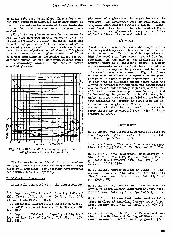
Shaw and Jacoby: Glass and Its Properties
of about 13°C over No.12 glass. In many instancesthe tube stems made of No.816 glass have shown asbad electrolysis as those made of No.12 glass dueto the fact that the stems were very poorly an-nealed.
All of the resistance values in the curves inFig. 10 were measured on well -annealed glass. Asstated previously, a poorly annealed glass hasfrom 33 to 40 per cent of the resistance of well -annealed glass. It will be seen that the reduc-tion in electrolysis expected when No.816 glassis substituted for No.12 glass would be nullifiedby a poor annealing of the No.816 glass. The re-sistance curves of the different glasses wouldbe considerably lowered in the case of poorlyannealed glasses.
ROOM TEMPERATURE
a
3
2
0.1
4
0 2 4 6 8 10 12 14
FREQUENCY - MEGACYCLES16
IR
7xcr
6
5<zU)
-1
0:0
Cr0
3 ce0
2
00-
01/3
Fig. 11 - Effect of frequency on power factorof glasses at room temperature.
The factors to be considered for minimum elec-trolysis are: high electrical -resistance glass;glass well annealed; low operating temperature;and maximum lead -wire spacing.
B. Dielectric Properties
Intimately connected with the electrical re -
5 J. Hopkinson,"Electrostatic Capacity of Glass,"Phil. Trans. of Roy. Soc. of London, Vol. 168,pp. 17-23 and plate 2; 1878.
J. Hopkinson,"Electrostatic Capacity of Glass,"Proc. of Roy. Soc. of London, Vol. 31, pp. 148-149; 1880.
J. Hopkinson,"Dielectric Capacity of Liquids,"Proc. of Roy. Soc. of London, Vol. 31, pp. 347-348; 1881.
sistance of a glass are its properties as a di-electric. The dielectric constant will range inthe usual soft glasses between 6 and 8. Hopkin-son5 found that the dielectric constant for aseries of lead glasses with varying quantitiesof lead followed the general relation
k/d = 2.2
The dielectric constant is somewhat dependent onfrequency and temperature but not in such a manneras to be serious. Variation with temperature athigh frequencies is less marked than at low fre-quencies. In the case of the dielectric loss,however, there is a different story. A numberof measurements madebyP. A. Richards and othersin this laboratory on the glasses used in radio -tube manufacture are shown in Fig. 11. Thesecurves show the effect of frequency on the powerfactor of glasses at room temperature. It willbe seen that in all cases except Nonex glass thecurves go through a minimum when the measurementsare carried to sufficiently high frequencies. Theeffect of raising the temperature is very markedin increasing the power factor in all cases, butunfortunately, there is not sufficient systematicdata available to present in curve form the in-formation on our glasses. Measurements on otherglasses indicate that a threefold increase inpower factor may be expected from a rise in temp-erature of 100°C.
BIBLIOGRAPHY
E. M. Guyer, "The Electrical Behavior of Glass atRoom Temperature;' Jour. Amer. Ceramic Soc., Vol.16, No.12, pp. 607-618; 1933.
Hodkinend Cousen, "Textbook of Glass Technology."(Second Edition) 1929, D. Van Nostrand Co., Inc.
H. R. Kiehl, "The Electrical. Conductivity ofGlass," Parts I and II, Physics, Vol. 5, No.12,pp. 363-369 and 370-373; 1934. Part III, Vol. 7,No.1, pp. 20-25; 1936.
H. R. Lillie, "Stress Release in Glass -A Phe-nomenon Involving Viscosity as a Variable withTime," Jour. Amer. Ceramic Soc., Vol. 19, No.2,
PP. 45-54; 1936.
H. R. Lillie, "Viscosity of Glass between theStrain Point and Melting Temperature," Jour. Amer.Ceramic Soc., Vol. 14, No.7, pp. 502-511; 1931.
H. R. Lillie, "Viscosity -Time -Temperature Rela-tions in Glass at Annealing Temperature," Jour.,Amer. Ceramic Soc., Vol. 16, No.12, pp. 619-631;1933.
J. T. Littleton, "The Physical Processes Occur-ring in the Melting and Cooling of Glass," Jour.Amer. Ceramic Soc.,Vol.17, No.3, pp .43 -49; 1934.
101

Vacuum Tube Design
J. T. Littleton, "The Effect of Heat Treatmenton the Physical Properties of Glass," Bulletinof Amer. Ceramic Soc., Vol. 15, No.9, pp. 306-311; 1936.
Littleton and Morey, "The Electrical Propertiesof Glass." (First Edition) 1933, John Wiley &
Sons.
Littleton and Wetmore, "The Electrical Conduc-tivity of Glass in the Annealing Zone as a Func-tion of Time and Temperature," Jour. Amer. Cer-amic Soc., Vol. 19, No.9, pp. 243-245; 1936.
George W. Morey, "Constitution of Glass," Jour.Amer. Ceramic Soc., Vol. 17, No.11, pp. 315-328;1934.
George W. Morey, "Annealing of Pyrex ChemicalResistant Glass," Ind. and Eng. Chem. (Indust.
Edition), Vol. 27, No.8, pp. 966-971; 1934.
Morey and Littleton, "Phase Equilibrium Relation-ships Determining Glass Composition," "Critical
Temperature in Silicate Glasses," Ind. and Eng.
Chem. (Indust. Ed.), Vol. 25, No.7, pp. 742-755;1933.
W. E. S. Turner, "The Chemical Durability ofGlass," Bulletin of Amer. Ceramic Soc., Vol. 14,No.5, pp. 165-169; 1935.
102

Lecture 10
CONSTRUCTION TRENDS IN RADIO TUBES
N. R. Smith
The structural design of radio tubes is a verycomprehensive subject. To go into the detailedmechanical design of the parts and electrodesentering into the fabrication of vacuum tubeswould involve a great many formulae, tabulationsand design factors that would require much morespace and time than has been apportioned to thissubject. Consequently, this lecture will be de-voted to a short historical review of the variousmechanical constructions used and a descriptionof the various types of electrodes now available.A comparison of the present with the earlier
constructions will serve to indicate the improve-ments made and will provide a more complete un-derstAnding of the problems involved in struc-tural design.
EDISON hITILT
The phenomenon which has played so importanta part in the development of the radio tube wasfirst noted by Thomas A. Edison in 1881. Withan experimental device similar to that shown inFig. 1, Edison discovered that when an electrodewas interposed between the legs of an incandes-
Fig. 1 - Edison's experimental lamp with anelectrode interposed between legs of the in-candescent filament and connected to thepositive end of the filament.
cent filament and was connected to the positiveend of the filament, a current would flow betweenthat electrode and the positive filament termi-nal. This phenomenon was called the "Edison ef-fect," and a patent was issued covering it in1884. The parts used in this experimental devicewere the same as were then being used in the manu-facture of carbon -filament incandescent lampswhich had been developed by Edison during theprevious two years. It is interesting to note,
that for all practical considerations, the fun-damental design of enclosure suggested in thisdevice fifty-five years ago has been retained onmany tubes manufactured today, and until the ad-vent of the dome -top bulb in 1932, was the mostprevalent design used by American tube manufac-turers.
FLEMING VALVE
For the succeeding twenty-four years, follow-ing Edison's discovery, no practical applicationwas made of the "Edison effect." The first com-mercial application was made by Professor.]: A.Fleming in 1905 when he developed the two -elec-trode tube, "Fleming valve," and suggested thatit be used for the rectification of alternatingcurrents. One type of Fleming valve is shown inFig. 2. The similarity of this tube to severalmodern rectifiers is apparent.
Fig. 2 - One type of Fleming valve.
DeFOREST AUDION
The following year, 1906, r. Lee DeForestadded a third electrode, a grid, between thecathode and plate. This grid provided a meansfor controlling the current passing through thetube. In these first tubes, such as is illus-trated in Fig. 3, Dr. DeForest made use of twostandard lamp flanges sealed into opposite endsof a G-16-1/2 type bulb. The filament was sup-ported from one flange and the leads were broughtout to a standard mogul screw base. The grid andplate were supported from the opposite flange.The 25 -mil nickel grid lead was formed insidethe tube into a zigzag shape with spaces betweenadjacent zigzags varying between 3/64" and 3/32".The plate consisted of a piece of 5 -mil nickelribbon, 9/16" square, scribed and sheared out by
103
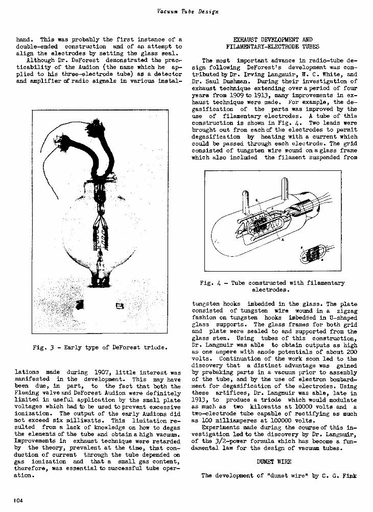
Vacuum Tube Design
hand. This was probably the first instance of adouble -ended construction and of an attempt toalign the electrodes by setting the glass seal.
Although Dr. DeForest demonstrated the prac-ticability of the Audion (the name which he ap-plied to his three -electrode tube) as a detectorand amplifier of radio signals in various instal -
Fig. 3 - Early type of DeForest triode.
lations made during 1907, little interest wasmanifested in the development. This may havebeen due, in part, to the fact that both theFleming valve and DeForest Audion were definitelylimited in useful application by the small platevoltages which had to be used to prevent excessiveionization. The output of the early Audions didnot exceed six milliwatts. This limitation re-sulted from a lack of knowledge on how to degasthe elements of the tube and obtain a high vacuum.Improvements in exhaust technique were retardedby the theory, prevalent at the time, that con-duction of current through the tube depended ongas ionization and that a small gas content,therefore, was essential to successful tube oper-ation.
EXHAUST DEVELOPMENT ANDFILAMENTARY-ELPCTRODE TUBES
The most important advance in radio -tube de-sign following DeForest's development was con-tributed by Dr. Irving Langmuir, W. C. White, andDr. Saul Dushman. During their investigation ofexhaust technique extending over a period of fouryears from 1909 to 1913, many improvements in ex-haust technique were made. For example, the de -
gasification of the parts was improved by theuse of filamentary electrodes. A tube of thisconstruction is shown in Fig. 4. Two leads werebrought out from each of the electrodes to permitdegasification by heating with a current whichcould be passed through each electrode. The gridconsisted of tungsten wire wound on aglass framewhich also included the filament suspended from
Fig. 4 - Tube constructed with filamentaryelectrodes.
tungsten hooks imbedded in the glass. The plateconsisted of tungsten wire wound in a zigzagfashion on tungsten hooks imbedded in U-shapedglass supports. The glass frames for both gridand plate were sealed to and supported from theglass stem. Using tubes of this construction,Dr. Langmuir was able to obtain outputs as highas one ampere with anode potentials of about 200volts. Continuation of the work soon led to thediscovery that a distinct advantage was gainedby prebaking parts in a vacuum prior to assemblyof the tube, and by the use of electron bombard-ment for degasification of the electrodes. Usingthese artifices, Dr. Langmuir was able, late in1913, to produce a triode which would modulateas much as two kilowatts at 10000 volts and atwo -electrode tube capable of rectifying as muchas 100 milliamperes at 100000 volts.
Experiments made during the course of this in-vestigation led to the discovery by Dr. Langmuir,of the 3/2 -power formula which has become a fun-damental law for the design of vacuum tubes.
DUMET WIRE
The development of "dumet wire" by C. G. Fink
104

Smith: Construction Trends in Radio Tubes
and its application to lamp -manufacturing prac-tice in 1912 was one of the major improvementsin constructional procedure. The dumet wire usedin making the vacuum -tight seal to glass had muchbetter thermal and electrical characteristicsthan the more expensive platinum press leadswhich it replaced. The initial production ofradio tubes in 1920 used this material whichstill remains the standard material for seals tosoft glass.
WEAGANT VALVE
Another interesting construction developed in1913 was the Weagant valve shown in Fig. 5. Inthis tube the conventional grid consisting of alattice interposed between cathode and plate wasreplaced by a grid external to the vacuum cham-ber. This external grid was in the form of acylindrical electrode concentrically aligned
PLATE
OUTSIDE ELECTRONCONTROL ELEMENT
FILAMENTLEADS
GLASSSUPPORT
PLATE
FILAMENT
GLASSSUPPORT
Fig. 5 - (left) The Weagant valve with the out-side electrostatic control element in position.
(right) The same valve with the con-trol element removed.
with the cathode stream. Although a tube withthis construction was somewhat less expensive tomanufacture, its low sensitivity and its limita-tions as an amplifier when compared with theDeForest type made it unsatisfactory for commer-cial development.
TELEPHONE REPEATER TUBESWITH OXIDE -COATED FILAMENTS
In 1912 the Western Electric Company becameinterested in the Audion for use as a repeateror booster in telephonic communication. A tubesimilar to that shown in Fig. 6 was designed andplaced in service in 1915 to establish the firsttranscontinental telephone service. The elec-trodes were enclosed in aG-18 bulb and the leadsbrought out to a molded composition four -pin
base. The stem had a formed -cane glass supportsealed to one end of the press. Various tungsten -wire supports were imbedded in the cane and servedto hold the electrodes in correct relationship.The filament was platinum coated with barium ox-ide. This filament gave much better emissionthan the pure tungsten filaments then commonlyused. Although the oxide -coated filament was de-veloped by the Western Electric Company in 1914,it was not utilized by other manufacturers untilthe Westinghouse Electric and Manufacturing Com-pany announced the WD -11 in 1920. The grid usedin the repeater tube consisted of parallel tung-sten wires welded across nickel side -rods. Thegrids were made in strip and folded to form thetwo sides. Of especial interest to the engineerconcerned with end loss is the filament mounting.The ends of the filament were clamped into theends of 25 -mil copper leads which were sealed
Fig. 6 - Early type of Western Electric triode.
into the glass stem press. However, tubes ofthis early design were fundamentally satisfactoryand with slight modifications are still produced.
TUBES DEVELOPED IN EUROPE FOR WAR SERVICE
The World War served in 1914 to stimulate fur-ther development of the radio tube. The valueof this device for use in both telegraphic andtelephonic communication under front-line condi-tions was recognized and so the French began de-velopment of simple, rugged tubes which could bemade in quantity with uniform characteristics.One tube used extensively during the latter yearsof the War is shown in Fig. 7. The tube had aG-16-1/2 bulb and a molded composition base withlong pins. The electrodes were mounted horizon-tally. This type of construction has been re-tained abroad especially in Holland and Germany,
105
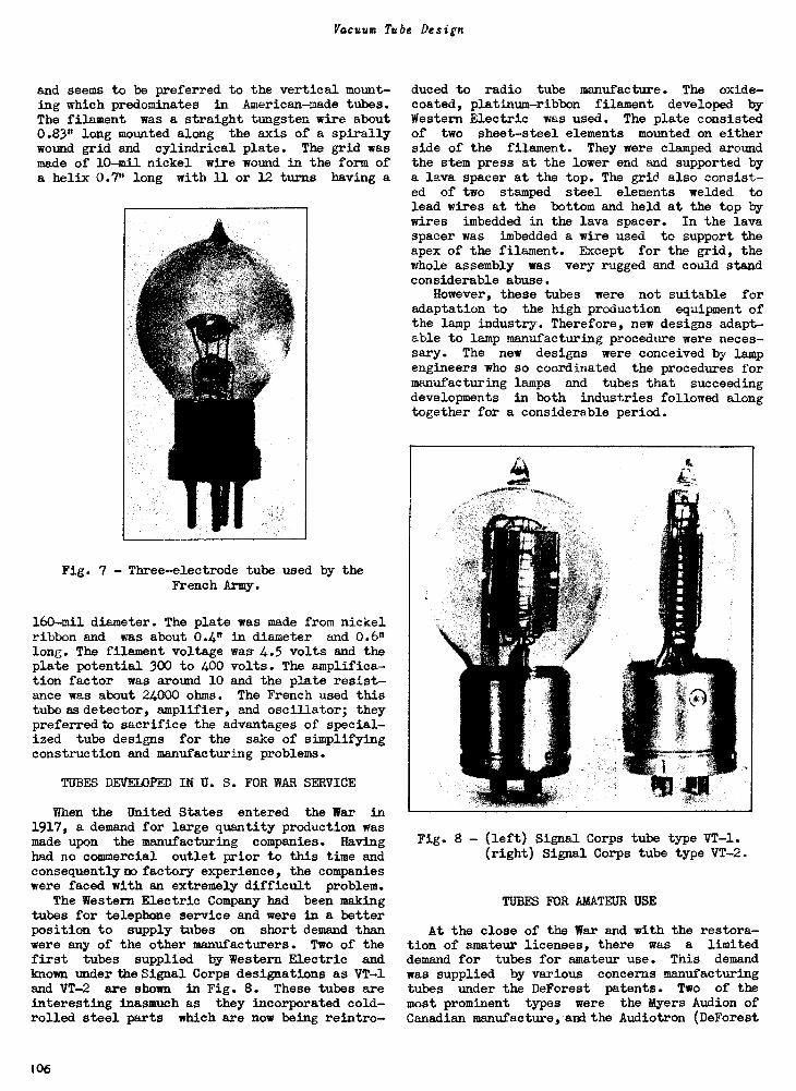
Vacuum Tube Design
and seems to be preferred to the vertical mount-ing which predominates in American -made tubes.The filament was a straight tungsten wire about0.83" long mounted along the axis of a spirallywound grid and cylindrical plate. The grid wasmade of 10 -mil nickel wire wound in the form ofa helix 0.7" long with 11 or 12 turns having a
Fig. 7 - Three -electrode tube used by theFrench Army.
160 -mil diameter. The plate was made from nickelribbon and was about 0.4" in diameter and 0.6"long. The filament voltage was 4.5 volts and theplate potential 300 to 400 volts. The amplifica-tion factor was around 10 and the plate resist-ance was about 24000 ohms. The French used thistube as detector, amplifier, and oscillator; theypreferred to sacrifice the advantages of special-ized tube designs for the sake of simplifyingconstruction and manufacturing problems.
TUBES DEVELOPED IN U. S. FOR WAR SERVICE
When the United States entered the War in1917, a demand for large quantity production wasmade upon the manufacturing companies. Havinghad no commercial outlet prior to this time andconsequently no factory experience, the companieswere faced with an extremely difficult problem.
The Western Electric Company had been makingtubes for telephone service and were in a betterposition to supply tubes on short demand thanwere any of the other manufacturers. Two of thefirst tubes supplied by Western Electric andknown under the Signal Corps designations as VT-iand VT -2 are shown in Fig. 8. These tubes areinteresting inasmuch as they incorporated cold -rolled steel parts which are now being reintro-
duced to radio tube manufacture. The oxide -
coated, platinum -ribbon filament developed byWestern Electric was used. The plate consistedof two sheet -steel elements mounted on eitherside of the filament. They were clamped aroundthe stem press at the lower end and supported bya lava spacer at the top. The grid also consist-ed of two stamped steel elements welded tolead wires at the bottom and held at the top bywires imbedded in the lava spacer. In the lavaspacer was imbedded a wire used to support theapex of the filament. Except for the grid, thewhole assembly was very rugged and could standconsiderable abuse.
However, these tubes were not suitable foradaptation to the high production equipment ofthe lamp industry. Therefore, new designs adapt-able to lamp manufacturing procedure were neces-sary. The new designs were conceived by lampengineers who so coordinated the procedures formanufacturing lamps and tubes that succeedingdevelopments in both industries followed alongtogether for a considerable period.
Fig. 8 - (left) Signal Corps tube type VT -1.(right) Signal Corps tube type VT -2.
TUBES FOR AMATEUR USE
At the close of the War and with the restora-tion of amateur licenses, there was a limiteddemand for tubes for amateur use. This demandwas supplied by various concerns manufacturingtubes under the DeForest patents. Two of themost prominent types were the Myers Audion ofCanadian manufacture, aed the Audiotron (DeForest
106
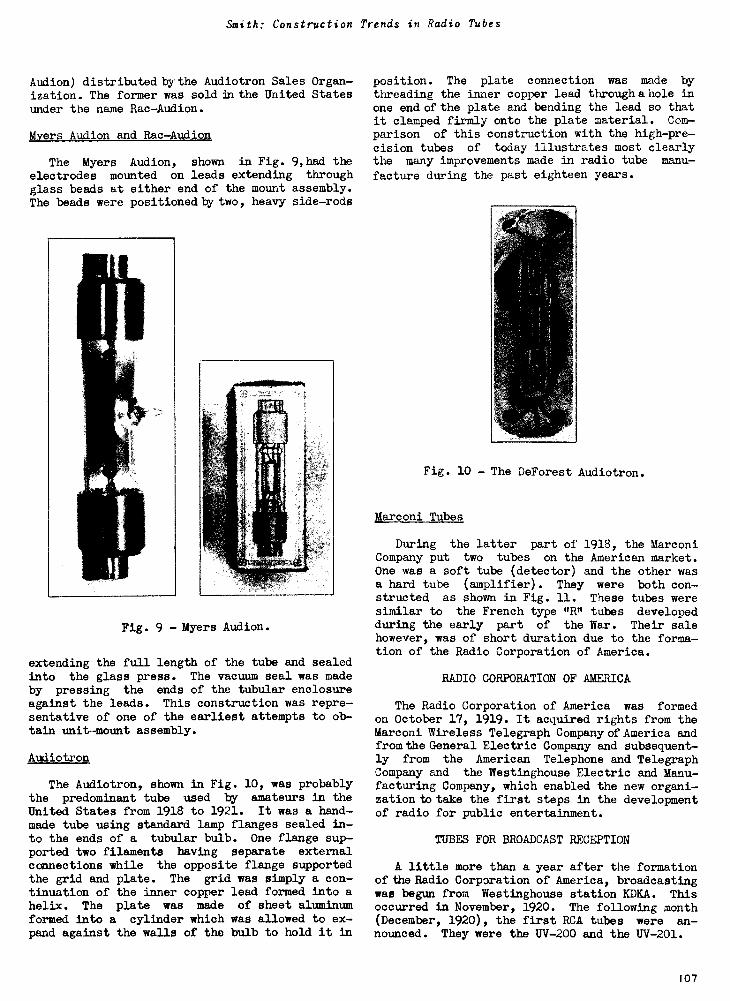
Smith: Construction Trends in Radio Tubes
Audion) distributed by the Audiotron Sales Organ-ization. The former was sold tithe United Statesunder the name Rac-Audion.
Myers Audion and Rac-Audion
The Myers Audion, shown in Fig. 9,had theelectrodes mounted on leads extending throughglass beads at either end of the mount assembly.The beads were positioned by two, heavy side -rods
Fig. 9 - Myers Audion.
extending the full length of the tube and sealedinto the glass press. The vacuum seal was madeby pressing the ends of the tubular enclosureagainst the leads. This construction was repre-sentative of one of the earliest attempts to ob-tain unit -mount assembly.
Audiotron
The Audiotron, shown in Fig. 10, was probablythe predominant tube used by amateurs in theUnited States from 1918 to 1921. It was a hand-made tube using standard lamp flanges sealed in-to the ends of a tubular bulb. One flange sup-ported two filaments having separate externalconnections while the opposite flange supportedthe grid and plate. The grid was simply a con-tinuation of the inner copper lead formed into ahelix. The plate was made of sheet aluminumformed into a cylinder which was allowed to ex-pand against the walls of the bulb to hold it in
position. The plate connection was made bythreading the inner copper lead through a hole inone end of the plate and bending the lead so thatit clamped firmly onto the plate material. Com-parison of this construction with the high -pre-cision tubes of today illustrates most clearlythe many improvements made in radio tube manu-
facture during the past eighteen years.
Fig. 10 - The DeForest Audiotron.
Marconi Tubes
During the latter part of 1918, the MarconiCompany put two tubes on the American market.One was a soft tube (detector) and the other wasa hard tube (amplifier). They were both con-structed as shown in Fig. 11. These tubes weresimilar to the French type "R" tubes developedduring the early part of the War. Their salehowever, was of short duration due to the forma-tion of the Radio Corporation of America.
RADIO CORPORATION OF AMERICA
The Radio Corporation of America was formedon October 17, 1919. It acquired rights from theMarconi Wireless Telegraph Company of America andfrom the General Electric Company and subsequent-ly from the American Telephone and TelegraphCompany and the Westinghouse Electric and Manu-facturing Company, which enabled the new organi-zation to take the first steps in the developmentof radio for public entertainment.
TUBES FOR BROADCAST RECEPTION
A little more than a year after the formationof the Radio Corporation of America, broadcastingwas begun from Westinghouse station KDKA. Thisoccurred in November, 1920. The following month(December, 1920), the first RCA tubes were an-nounced. They were the UV -200 and the UV -201.
107
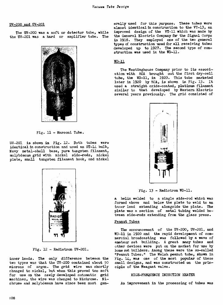
Vacuum Tube Design
UV -200 and UV -201
The UV -200 was a soft or detector tube, whilethe UV -201 was a hard or amplifier tube. The
Fig. 11 - Marconi Tube.
UV -201 is shown in Fig. 12. Both tubes wereidentical in construction and used an ST -14 bulb,
Navy metal -shell base, pure tungsten filament,molybdenum grid with nickel side -rods, nickelplate, small tungsten filament hook, and nickel
Fig. 12 - Radiotron UV -201.
inner leads. The only difference between thetwo types was that the UV -200 contained about 50microns of argon. The grid wire was shortlychanged to nickel, but when this proved too softfor use on the newly developed automatic gridmachines, the wire was changed to Nichrome. Ni-chrome and molybdenum have since been most gen-
erally used for this purpose. These tubes werealmost identical in construction to the VT -13, an
improved design of the VT -11 which was made bythe General Electric Company for the Signal Corpsin 1918. They employed one of the two generaltypes of construction used for all receiving tubesdeveloped up to 1927. The second type of con-struction was used in the WD -11.
WD -11
The Westinghouse Company prior to its associ-ation with RCA brought out the first dry -celltube, the WD -11, in 1920. This tube marketedlater in 1920 by RCA, is shown in Fig. 13. It
used a straight oxide -coated, platinum filamentsimilar to that developed by Western Electricseveral years previously. The grid consisted of
Fig. 13 - Radiotron WD -11.
a helix welded to a single side -rod which wasformed above and below the plate to weld to aninner lead extending alongside the plate. Theplate was a section of metal tubing welded be-tween side -rods extending from the glass press.
Peanut Tubes
The announcement of the UV -200, UV -201, and
WD -11 in 1920 and the rapid development of com-mercial broadcasting was followed by a wave ofamateur set building. A great many tubes and
other devices were put on the market for use byhome set builders. Among these were the so-called"Peanut Tubes." The Welsh peanut tube, shown inFig. 14, was one of the most popular of thesesmall designs, and was constructed on the prin-ciple of the Weagant valve.
HIGH FREQUENCY INDUCTION HEATER
An improvement in the processing of tubes was
108
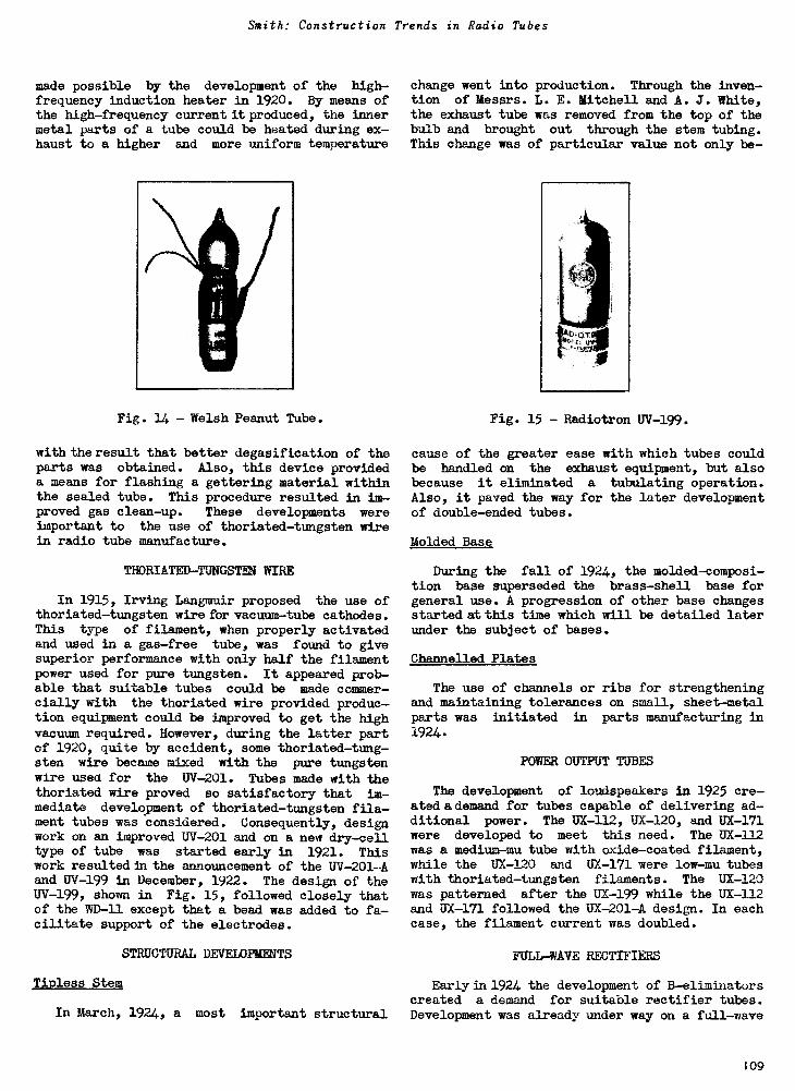
Smith: Construction Trends in Radio Tubes
made possible by the development of the high -
frequency induction heater in 1920. By means ofthe high -frequency current it produced, the innermetal parts of a tube could be heated during ex-haust to a higher and more uniform temperature
Fig. 14 - Welsh Peanut Tube.
with the result that better degasification of theparts was obtained. Also, this device provideda means for flashing a gettering material withinthe sealed tube. This procedure resulted in im-proved gas clean-up. These developments wereimportant to the use of thoriated-tungsten wirein radio tube manufacture.
THORIATED-TUNGSTEN WIRE
In 1915, Irving Langmuir proposed the use ofthoriated-tungsten wire for vacuum -tube cathodes.This type of filament, when properly activatedand used in a gas -free tube, was found to givesuperior performance with only half the filamentpower used for pure tungsten. It appeared prob-able that suitable tubes could be made commer-cially with the thoriated wire provided produc-tion equipment could be improved to get the highvacuum required. However, during the latter partof 1920, quite by accident, some thoriated-tung-sten wire became mired with the pure tungstenwire used for the UV 201. Tubes made with thethoriated wire proved so satisfactory that im-mediate development of thoriated-tungsten fila-ment tubes was considered. Consequently, designwork on an improved UV -201 and on a new dry -celltype of tube was started early in 1921. Thiswork resulted in the announcement of the UV -201-Aand UV -199 in December, 1922. The design of theUV -199, shown in Fig. 15, followed closely thatof the WD -11 except that a bead was added to fa-cilitate support of the electrodes.
STRUCTURAL DEVELOPMENTS
Tipless Stem
In March, 1924, a most important structural
change went into production. Through the inven-tion of Messrs. L. E. Mitchell and A. J. White,the exhaust tube was removed from the top of thebulb and brought out through the stem tubing.This change was of particular value not only be -
Fig. 15 - Radiotron UV -199.
cause of the greater ease with which tubes couldbe handled on the exhaust equipment, but alsobecause it eliminated a tubulating operation.Also, it paved the way for the later developmentof double -ended tubes.
Molded Base
During the fall of 1924, the molded -composi-tion base superseded the brass -shell base forgeneral use. A progression of other base changesstarted at this time which will be detailed laterunder the subject of bases.
Channelled Plates
The use of channels or ribs for strengtheningand maintaining tolerances on small, sheet -metalparts was initiated in parts manufacturing in1924.
POWER OUTPUT TUBES
The development of loudspeakers in 1925 ere-atedademand for tubes capable of delivering ad-ditional power. The UX-112, UX-120, and UX-171were developed to meet this need. The UX-ii,was a medium -mu tube with oxide -coated filament,while the UX-120 and UX-171 were low -mu tubeswith thoriated-tungsten filaments. The UX-120was patterned after the UX-199 while the UX-112and UX-171 followed the UX-201-A design. In eachcase, the filament current was doubled.
FULL -WAVE RECTIFIERS
Early in 1924 the development of B -eliminatorscreated a demand for suitable rectifier tubes.Development was already under way on a full -wave
109
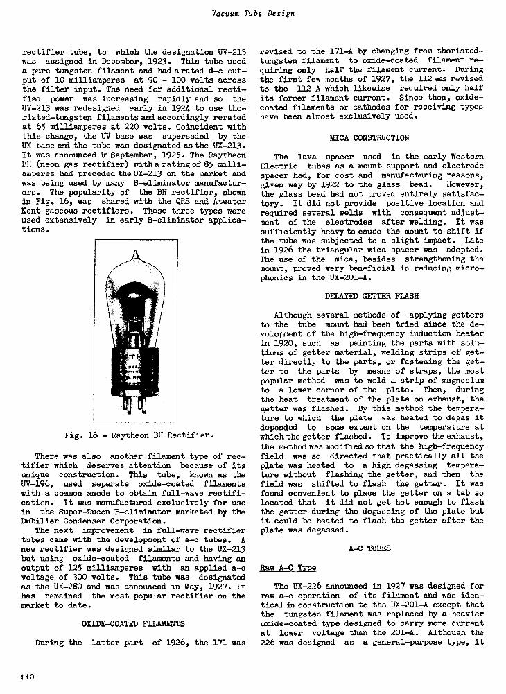
Vacuum Tube Design
rectifier tube, to which the designation UV -213was assigned in December, 1923. This tube useda pure tungsten filament and had a rated d -c out-put of 10 milliamperes at 90 - 100 volts acrossthe filter input. The need for additional recti-fied power was increasing rapidly and so theUV -213 was redesigned early in 1924 to use the-riated-tungsten filaments and accordingly reratedat 65 milliamperes at 220 volts. Coincident withthis change, the DV base was superseded by theUX base arxi the tube was designated as the UX-213.It was announced in September, 1925. The RaytheonBH (neon gas rectifier) witharatingof 85 milli-amperes had preceded the UX-213 on the market andwas being used by many B -eliminator manufactur-ers. The popularity of the BH rectifier, shownin Fig. 16, was shared with the QRS and AtwaterKent gaseous rectifiers. These three types wereused extensively in early B -eliminator applica-tions.
Fig. 16 - Raytheon BH Rectifier.
There was also another filament type of rec-tifier which deserves attention because of itsunique construction. This tube, known as theUV -196, used separate oxide -coated filamentswith a common anode to obtain full -wave rectifi-cation. It was manufactured exclusively for usein the Super-Ducon B -eliminator marketed by theDubilier Condenser Corporation.
The next improvement in full -wave rectifiertubes came with the development of a -c tubes. Anew rectifier was designed similar to the UX-213but using oxide -coated filaments and having anoutput of 125 milliamperes with an applied a -cvoltage of 300 volts. This tube was designatedas the UX-280 and was announced in May, 1927. Ithas remained the most popular rectifier on themarket to date.
OXIDE -COATED FILAMENTS
During the latter part of 1926, the 171 was
revised to the 171-A by changing from thoriated-tungsten filament to oxide -coated filament re-quiring only half the filament current. Duringthe first few months of 1927, the 112wes revisedto the 112-A which likewise required only half
its former filament current. Since then, oxide -coated filaments or cathodes for receiving typeshave been almost exclusively used.
MICA CONSTRUCTION
The lava spacer used in the early WesternElectric tubes as a mount support and electrodespacer had, for cost and manufacturing reasons,given way by 1922 to the glass bead. However,the glass bead had not proved entirely satisfac-tory. It did not provide positive location andrequired several welds with consequent adjust-ment of the electrodes after welding. It wassufficiently heavy to cause the mount to shift ifthe tube was subjected to a slight impact. Latein 1926 the triangular mica spacer was adopted.The use of the mica, besides strengthening themount, proved very beneficial in reducing micro -phonics in the UX -201-A.
DELAYED GETTER FLASH
Although several methods of applying gettersto the tube mount had been tried since the de-velopment of the high -frequency induction heaterin 1920, such as painting the parts with solu-tions of getter material, welding strips of get-ter directly to the parts, or fastening the get-ter to the parts by means of straps, the mostpopular method was to weld a strip of magnesiumto a lower corner of the plate. Then, duringthe heat treatment of the plate on exhaust, thegetter was flashed. By this method the tempera-ture to which the plate was heated to degas itdepended to some extent on the temperature atwhich the getter flashed. To improve the exhaust,
the method was modified so that the high -frequency
field was so directed that practically all theplate was heated to a high degassing tempera-ture without flashing the getter, and then the
field was shifted to flash the getter. It wasfound convenient to place the getter on a tab solocated that it did not get hot enough to flashthe getter during the degassing of the plate butit could be heated to flash the getter after theplate was degassed.
A -C TUBES
Raw A -C Type
The UX-226 announced in 1927 was designed forraw a -c operation of its filament and was iden-tical in construction to the UX-201-A except thatthe tungsten filament was replaced by a heavieroxide -coated type designed to carry more currentat lower voltage than the 201-A. Although the
226 was designed as a general-purpose type, it
110
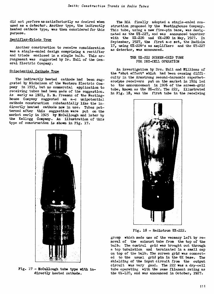
Smith: Construction Trends in Radio Tubes
did not perform as satisfactorily as desired whenused as a detector. Another type, the indirectlyheated cathode type, was then considered for thispurpose.
Rectifier -Triode Type
Another construction to receive considerationwas a single -ended design comprising a rectifierand triode enclosed in a single bulb. This ar-rangement was suggested by Dr. Hull of the Gen-eral Electric Company.
Unipotential Cathode Type
The indirectly heated cathode had been sug-gested by Nicholson of the Western Electric Com-pany in 1915, but no commercial application toreceiving tubes had been made of the suggestion.As early as 1921, H. M. Freeman of the Westing-house Company suggested an a -c unipotentialcathode construction substantially like the in-directly heated cathode now in use. Tubes pat-terned after this suggestion were put on themarket early in 1925 by McCullough and later bythe Kellogg Company. An illustration of thistype of construction is shown in Fig. 17.
Fig. 17 - McCullough tube type with in-directly heated cathode.
The RCA finally adopted a single -ended con-struction proposed by the Westinghouse Company.This tube, using a new five -pin base, was desig-nated as the UT -227, and was announced togetherwith the UX-226 and UX-280 in May, 1927. InSeptember, 1927, the first a -c set, the Radiola17, using UX-2261s as amplifiers and the UY -227as detector, was announced.
THE UX-222 SCREEN -GRID TUBEFOR DRY -CELL OPERATION
An investigation by Drs. Hull and Williams ofthe "shot effect" which had been causing diffi-culty in the Armstrong second -harmonic superhet-erodyne receivers put on the market in 1924 ledto the announcement in 1926 of the screen -gridtube, known as the UX-222. The 222, illustratedin Fig. 18, was the first tube in the receiving
Fig. 18 - Radiotron UX-222.
group which made use of the vacancy left by re-moval of the exhaust tube from the top of thebulb. The control grid was brought out througha top tubulation and terminated in a small capon top of the bulb. The screen grid was connect-ed to the usual grid pin in the UX base. Theshielding of the input circuit from the outputcircuit was very good. The 222 was a dry -celltube operating with the same filament rating asthe UX-120, and was announced in October, 1927.
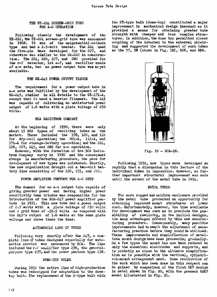
Vacuum Tube Design
THE UY-224 SCREEN -GRID TUBEFOR A -C OPERATION
Following closely the development of theDX -222011m UY-224 screen -grid tube was announcedin 1928. It was of the unipotential-cathodetype and had a 2.5 -volt heater. The 224 usedthe five -pin base developed for the 227, andotherwise was similar to the UX-222 in construc-tion. The 224, 226, 227, and 280 provided forthe r -f detector, 1st a -f, and rectifier needsof a -c sets, but no power output tube was as yetavailable.
THE UX-245 POWER OUTPUT TRIODE
The requirement for a power output tube ina-0 sets was fulfilled by the development of theUX-245, similar in all details to the UX-171-A,except that it used a heavier filament. The 245was capable of delivering an undistorted poweroutput of 1.6 watts with a plate voltage of 250volts.
RCA RADIOTRON COMPANY
At the beginning of 1930, there were onlyabout 15 RCA types of receiving tubes on the
market. These included the 199, 120, and 122for dry -cell operation; the 201-A, 112-A, and171-A for storage -battery operation; and the 224,226, 227, 245, and 280 for a -c operation.
However, with the formation of the RCA Radio-tron Compsny early in 1930 and the consequentchange in manufacturing procedure, the pace fordevelopment of new types was quickened. Shortly,the new organization brought out a two -volt bat-tery line consisting of the 230, 231, and 232.
POWER AMPLIFIER PENTODE FOR A -C SETS
The demand for an a -c output tube capable ofgiving greater power and having higher powersensitivity than triodes was responsible for theintroduction of the RCA -247 power amplifier pen-tode in 1931. This new tube had a power outputof 2.7 watts with a plate voltage of 250 voltsand a grid bias of -16.5 volts as compared withthe 245's output of 1.6 watts at the same platevoltage and three times the bias.
AUTOMOBILE LINE OF TUBES
Following very shortly after the 247, a com-plete line of tubes designed especially for auto-mobile service was announced by RCA. The lineincluded the r -f amplifier type 236, the general-purpose type 237, and the power pentode type 238.
DOME -TOP BULBS
During 1932 the entire line of high -productiontubes was redesigned for adaptation to the dome -top bulb. The replacement of the S -type bulb with
the ST -type bulb (dome -top) constituted a majorimprovement in mechanical design inasmuch as itprovided a means for obtaining greater tubestrength with cheaper and less complex struc-tures. In addition, the dome top permitted closercoupling of the internal to the external shield-ing and suggested the development of such tubesas the 57, 58 (shown in Fig. 19), 6C6, and 6D6.
Fig. 19 - RCA -58.
Following 1932, new types were developed sorapidly that a discussion in this lecture of theindividual tubes is impossible. However, no fur-ther important structural improvement was madeuntil the advent of the metal tube in 1934.
METAL TUBES
The more rugged and uniform enclosure providedby the metal tube presented an opportunity forobtaining improved mount structures at lowercost. Unfortunately, however, the time availablefor development was such as to preclude the pos-sibility of realizing, in the initial designs,the many advantages offered by this new manufac-turing procedure. Consequently, many possibleimprovements had to await the adjustment of manu-facturing practice before they could be utilized.These improvements and simplification of metal -tube mount design have been proceeding gradually.On a few types the mount has now been reduced toonly the essential electrodes and supports, andis probably as close to the ultimate simplifica-tion as is possible with the vertical, cylindri-cal -mount arrangement used. Some realization ofthe work which has been done in this respect canbe gained by comparison of the first 6K7 designin metal shown in Fig. 20, with the present 6SK7mount illustrated in Fig. 21.
112
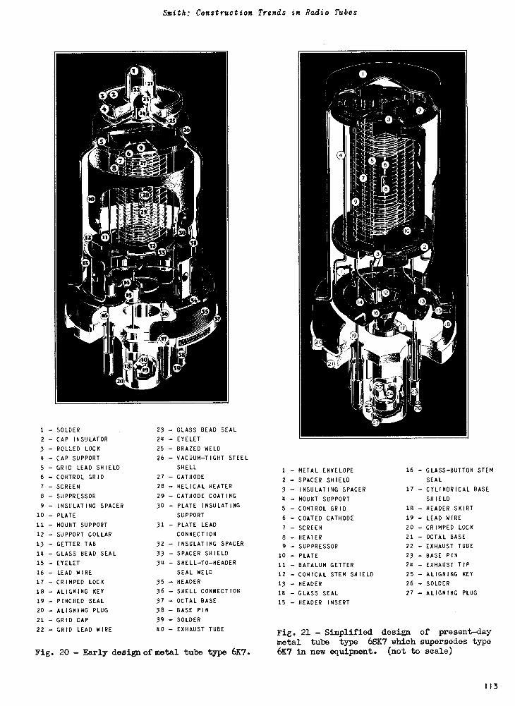
Smith: Construction Trends in Radio Tubes
1
2
3
It
5
6
7
8
9
10
11
12
13
14
15
16
17
18
19
20
21
22
1
1121
22,
4
S
10
12 1111
13
2
96 --;___Jio;
7 2074
8 sk=.5A
17
25
26
SO
33
39
31
34
35
S
- SOLDER
- CAP INSULATOR
- ROLLED LOCK
- CAP SUPPORT
- GRID LEAD SHIELD
- CONTROL GRID
- SCREEN
- SUPPRESSOR
- INSULATING SPACER
- PLATE
- MOUNT SUPPORT
- SUPPORT COLLAR
- GETTER TAB
- GLASS BEAD SEAL
- EYELET
- LEAD WIRE
- CRIMPED LOCK
- ALIGNING KEY
- PINCHED SEAL
- ALIGNING PLUG
- GRID CAP
- GRID LEAD WIRE
23
24
25
26
27
28
29
30
- GLASS BEAD SEAL
- EYELET
-
-
-
-
-
-
31 -
32 -
33 -
34 -
35 -
36 -
37 -
2
21
4
9
19
7
14
3
56
8
trm-jafr
0
12
16
41
2224.)
25 I 1
2 H
17
2
2
13
23
26
15
18
BRAZED WELD
VACUUM -TIGHT STEEL
SHELL1 - METAL ENVELOPE 16 - GLASS -BUTTON STEM
CATHODE2 - SPACER SHIELD SEAL
HELICAL HEATER3 - INSULATING SPACER 17 - CYLINDRICAL BASE
CATHODE COATING4 - MOUNT SUPPORT SHIELD
PLATE INSULATING5 - CONTROL GRID 18 - HEADER SKIRT
SUPPORT6 - COATED CATHODE 19 - LEAD WIRE
PLATE LEAD7 - SCREEN 20 - CRIMPED LOCK
CONNECTION8 - HEATER 21 - OCTAL BASE
INSULATING SPACER9 - SUPPRESSOR 22 - EXHAUST TUBE
SPACER SHIELD 10 - PLATE 23 - BASE PINSHELL -TO -HEADER 11 - BATALUM GETTER 24 - EXHAUST TIPSEAL WELD 12 - CONICAL STEM SHIELD 25 - ALIGNING KEYHEADER 13 - HEADER 26 - SOLDERSHELL CONNECTION 14 - GLASS SEAL 27 - ALIGNING PLUGOCTAL BASE 15 - HEADER INSERT
38 - BASE PIN
39 - SOLDER
40 - EXHAUST TUBE
Fig. 20 - Early design of metal tube type 6K7.
Fig. 21 - Simplified design of present-daymetal tube type 6SK7 which supersedes type6K7 in new equipment. (not to scale)
113
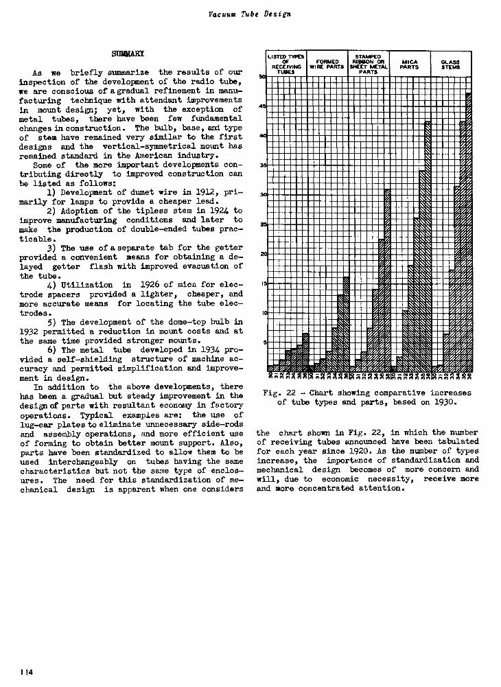
Vacuum Tube Design
SUMMARY
As we briefly summarize the results of ourinspection of the development of the radio tube,we are conscious of a gradual refinement in manu-
facturing technique with attendant improvementsin mount design; yet, with the exception of
metal tubes, there have been few fundamental
changes in construction. The bulb, base, and type
of stem have remained very similar to the firstdesigns and the vertical -symmetrical mount hasremained standard in the American industry.
Some of the more important developments con-tributing directly to improved construction canbe listed as follows:
1) Development of dumet wire in 1912, pri-marily for lamps to provide a cheaper lead.
2) Adoption of the tipless stem in 1924 toimprove manufacturing conditions and later to
make the production of double -ended tubes prac-ticable.
3) The use of a separate tab for the getterprovided a convenient means for obtaining a de-layed getter flash with improved evacuation ofthe tube.
4) Utilization in 1926 of mica for elec-trode spacers provided a lighter, cheaper, and
more accurate means for locating the tube elec-trodes.
5) The development of the dome -top bulb in1932 permitted a reduction in mount costs and atthe same time provided stronger mounts.
6) The metal tube developed in 1934 pro-vided a self -shielding structure of machine ac-curacy and permitted simplification and improve-ment in design.
In addition to the above developments, therehas been a gradual but steady improvement in thedesign of parts with resultant economy in factory
operations. Typical examples are: the use of
lug -ear plates to eliminate unnecessary side -rods
and assembly operations, and more efficient useof forming to obtain better mount support. Also,parts have been standardized to allow them to beused interchangeably on tubes having the samecharacteristics but not the same type of enclos-ures. The need for this standardization of me-chanical design is apparent when one considers
50
45
40
30
25
no
Is
LISTED TYPESOF FORMED
RECEIVING WI RE PARTSTUBES
STAMPEDRIBBON OR
SHEET METALPARTS
MICAPARTS
GLASSSTEMS
Y 4/4.\. 0...4%
./W
4'
N,MVI,:
, \0
4eV
\ .:.\k'
0004,
&,
7,,,, MY ;*$,A\ //f%
Y7'47 a.Nzw 0,, ;% :4.\:4
/ 43Sx. 11 /0.,7,7 NikS...\..-s
Nk7.4., "7: '\
..S. . /.43V &,.N., 7,4,A11111117,MMEMEM*MIMK07,0*MMEW07,4i;17W7,x-:7Y,4111/=MOIIIIMMW1M1M.\\IMerV,a7/El.'"' /AllIN07/27'.,7A=".:s:MMIIIKVAM7 /7 AIIMS:ri:::111F7r,7 ,7/411111KMMIWAW,2'M.
,-0*"//1-'7 \:,...1'S,z,4,4,..").7' .,:',X . .:*'8MM%' ' ,./"TaXe?..,',7) rat" -Am AXA;MRXrag;22 2,442,741m %
Fig. 22 - Chart showing comparative increasesof tube types and parts, based on 1930.
the chart shown in Fig. 22, in which the numberof receiving tubes announced have been tabulatedfor each year since 1920. As the number of typesincrease, the importance of standardization andmechanical design becomes of more concern andwill, due to economic necessity, receive moreand more concentrated attention.
1 14
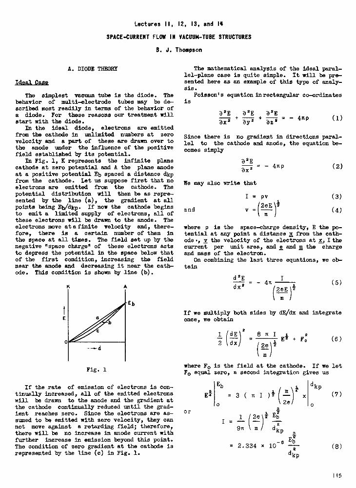
Lectures II, 12, 13, and 14
SPACE -CURRENT FLOW IN VACUUM -TUBE STRUCTURES
B. J. Thompson
A. DIODE THEORY
Ideal Case
The simplest vacuum tube is the diode. Thebehavior of multi -electrode tubes may be de-scribed most readily in terms of the behavior ofa diode. For these reasons our treatment willstart with the diode.
In the ideal diode, electrons are emittedfrom the cathode in unlimited numbers at zerovelocity and a part of these are drawn over tothe anode under the influence of the positivefield established by its potential.
In Fig. 1, 1 represents the infinite planecathode at zero potential and A the plane anodeat a positive potential Eb spaced a distance dkpfrom the cathode. Let us suppose first that noelectrons are emitted from the cathode. Thepotential distribution will then be as repre-sented by the line (a), the gradient at allpoints being Eb/dkp. If now the cathode beginsto emit a limited supply of electrons, all ofthese electrons will be drawn to the anode. Theelectrons move at a finite velocity and, there-fore, there is a certain number of them inthe space at all times. The field set up by thenegative "space charge" of these electrons actsto depress the potential in the space below thatof the first condition, increasing the fieldnear the anode and decreasing it near the cath-ode. This condition is shown by line (b).
E b
If the rate of emission of electrons is con-tinually increased, all of the emitted electronswill be drawn to the anode and the gradient atthe cathode continually reduced until the grad-ient reaches zero. Since the electrons are as-sumed to be emitted with zero velocity, they cannot move against a retarding field; therefore,there will be no increase in anode current withfurther increase in emission beyond this point.The condition of zero gradient at the cathode isrepresented by the line (c) in Fig. 1.
Tc I ) -§" -1 m
2e
= 2.334 x
The mathematical analysis of the ideal paral-lel -plane case is quite simple. It will be pre-sented here as an example of this type of analy-sis.
Poisson's equation in rectangular co-ordinatesis
.2a,rt '141 B 2 Eu
BX2 By2 Bz2 = - 4np (1)
Since there is no gradient in directions paral-lel to the cathode and anode, the equation be-comes simply
B2E
axe
We may also write that
and
- 4np (2)
I = pv1
.(2eEr( 3)
( 4)
where p is the space -charge density, E the po-tential at any point a distance x from the cath-ode., v the velocity of the electrons at x, I thecurrent per unit area, and e and m the chargeand mass of the electron.
On combining the last three equations, we ob-tain
d2E
dx2=
M
( 5 )
If we multiply both sides by dE/dx and integrateonce, we obtain
1 ILE)2 8 n I 2
E2 F02 \ dx) 2)71
1 in
(6)
where Fo is the field at the cathode. If we letFo equal zero, a second integration gives us
E4-
0Or
I =Eb
29n m dkp
Eba
2dkp
10-s
dkp
(7)
0
( 8 )
I15
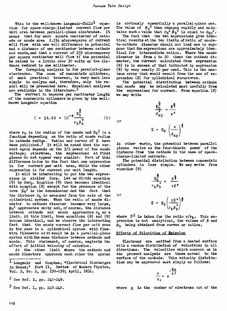
Vacuum Tube Design
This is the well-known Langmuir-Childl equa-tion for space -charge -limited current flow perunit area between parallel -plane electrodes. It
means that for each square centimeter of cath-ode or anode area 2.334 microamperes of currentwill flow with one volt difference in potentialand a distance of one centimeter between cathodeand anode, and that a current of 233 microamperesper square centimeter will flow if the potentialbe raised to a little over 30 volts or the dis-tance reduced to one millimeter.
The foregoing analysis is for parallel -planeelectrodes. The case of concentric cylinders,of much practical interest, is very much lesssimple to analyze and, therefore, only the re-sult will be presented here. Excellent analysesare available in the literature.2
The current in amperes per centimeter lengthof the concentric cylinders is given by the well-known Langmuir equation
E
I = 14.66 x 10⁻⁶b
2 (9)rbOb or
is obviously essentially a parallel -plane one.The value of gib2 then changes rapidly and main-tains such a value that rb20b2 is equal to dkp2.
The fact that the two expressions give iden-tical results at the two limits of ratio of anode -to -cathode diameter should not lead one to sup-pose that the expressions are approximately iden-tical for intermediate ratios. Where the anodediameter is from 4 to 20 times the cathode di-ameter, the current calculated from expression(8) is in excess of that indicated by expression(9) by very nearly 20 per cent. This is the max-imum error that would result from the use of ex-pression (8) for cylindrical structures.
The potential distribution between cathodeand anode may be calculated most usefully fromthe expressions for current. From equation (8)we may write
where rb is the radius of the anode and 0b2 is afunction depending on the ratio of anode radiusto cathode radius. Tables and curves of havebeen published.3 It will be noted that the cur-rent again depends on the 3/2 power of the anodevoltage; otherwise, the expressions at firstglance do not appear very similar. Part of thisdifference is due to the fact that one expressionis for current per unit area, while the otherexpression is for current per unit length.
It will be interesting to put the two expres-sions in similar form. Let us divide equation(9) by 2arb. Equation (9) then becomes identicalwith equation (8) except for the presence of theterm AO in the denominator and the fact that
the distance rb is measured from the axis of thecylindrical system. When the ratio of anode di-ameter to cathode diameter becomes very large,Ab2 approaches unity and, of course, the distancebetween cathode and anode approaches rb as alimit. At this limit, then equations (8) and (9)become identical, and we observe the interestingfact that the anode current flow per unit areais the same in a cylindrical system with fine -wire filaments as it would be in a parallel -planesystem with the same distance between cathode andanode. This statement, of course, neglects theeffect of initial velocity of emission.
At the other limit where the cathode andanode diameters approach each other the system
1 Langmuir and Compton, "Electrical Dischargesin Gases," Part II, Review of Modern Physics,Vol. 3, No. 2, Pp. 238-239; April, 1931.
2 See Ref. 1, pp. 245-249.
3 See Ref. 1, pp. 247-248.
1Eb
E2=
x2dkp
x t4
E = Eb ( ---dkp
In other words, the potential between parallelplanes varies as the four -thirds power of thedistance from the cathode in the case of space -charge -limited currents.
The potential distribution between concentriccylinders is less simple. We may write fromequation (9)
or
gb El
rbOb
E
r02
Eb(1. 134)rbOb
where 02 is taken for the ratio r/rk. This ex-pression is not analytical, the values of A andAb being obtained from curves or tables.
Effects of Velocities of Emission
Electrons are emitted from a heated surfacewith a random distribution of velocities in alldirections. The velocities which concern us inthe present analysis are those normal to thesurface of the cathode. This velocity distribu-tion may be expressed most simply as follows:
Een kT
e
no
where n is the number of electrons out of the
116
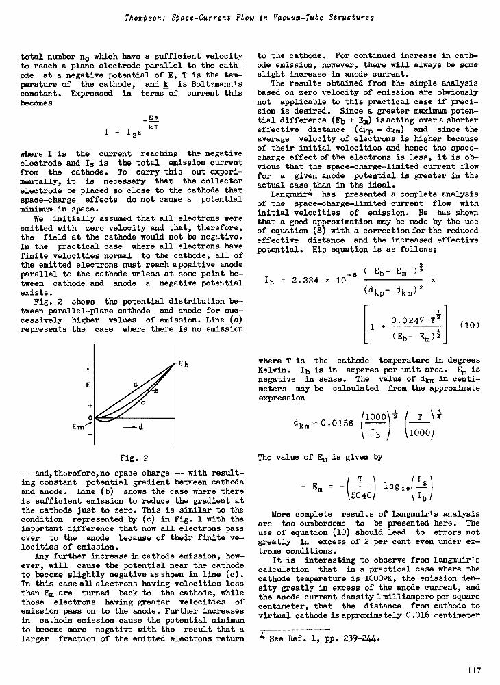
Thompson: Space -Current Flow in Vacuum -Tube Structures
total number no which have a sufficient velocityto reach a plane electrode parallel to the cath-ode at a negative potential of E, T is the tem-perature of the cathode, and k is Boltzmann'sconstant. Expressed in terms of current thisbecomes
_Ee
I =kT
where I is the current reaching the negativeelectrode and Is is the total emission currentfrom the cathode. To carry this out experi-mentally, it is necessary that the collectorelectrode be placed so close to the cathode thatspace -charge effects do not cause a potentialminimum in space.
We initially assumed that all electrons wereemitted with zero velocity and that, therefore,the field at the cathode would not be negative.In the practical case where all electrons havefinite velocities normal to the cathode, all ofthe emitted electrons must reach apositive anodeparallel to the cathode unless at some point be-tween cathode and anode a negative potentialexists.
Fig. 2 shows the potential distribution be-tween parallel -plane cathode and anode for suc-cessively higher values of emission. Line (a)represents the case where there is no emission
Eb
Ern
Fig. 2
and,therefore,no space charge -- with result-ing constant potential gradient between cathodeand anode. Line (b) shows the case where thereis sufficient emission to reduce the gradient atthe cathode just to zero. This is similar to thecondition represented by (c) in Fig. 1 with theimportant difference that now all electrons passover to the anode because of their finite ve-locities of emission.
Any further increase in cathode emission, how-ever, will cause the potential near the cathodeto become slightly negative as shown in line (c).In this case all electrons having velocities lessthan Em are turned back to the cathode, whilethose electrons having greater velocities ofemission pass on to the anode. Further increasesin cathode emission cause the potential minimumto become more negative with the result that alarger fraction of the emitted electrons return
to the cathode. For continued increase in cath-ode emission, however, there will always be someslight increase in anode current.
The results obtained from the simple analysisbased on zero velocity of emission are obviouslynot applicable to this practical case if preci-sion is desired. Since a greater maximum poten-tial difference (Eb + Em) is acting over a shortereffective distance (dkp - dkm) and since theaverage velocity of electrons is higher becauseof their initial velocities and hence the space -charge effect of the electrons is less, it is ob-vious that the space -charge -limited current flowfor a given anode potential is greater in theactual case than in the ideal.
Langmuir4 has presented a complete analysisof the space -charge -limited current flow withinitial velocities of emission. He has shownthat a good approximation may be made by the useof equation (8) with a correction for the reducedeffective distance and the increased effectivepotential. His equation is as follows:
Ib = 2.334 x 10⁻⁶( Eb- Em )i
(dkp- dkm)2
0.0247 T21
(Eb- Em)2
(10)
where T is the cathode temperature in degreesKelvin. Ib is in amperes per unit area. Em is
negative in sense. The value of dkm in centi-meters may be calculated from the approximateexpression
T )dkm=0.0156
1 3T
Ib 1000
The value of Em is given by
T- Em - login
Is
5040 Ib.
More complete results of Langmuir's analysisare too cumbersome to be presented here. The
use of equation (10) should lead to errors notgreatly in excess of 2 per cent even under ex-treme conditions.
It is interesting to observe from Langmuir'scalculation that in a practical case where thecathode temperature is 10000K, the emission den-sity greatly in excess of the anode current, andthe anode current density lmilliampere per squarecentimeter, that the distance from cathode tovirtual cathode is approximately 0.016 centimeter
4 See Ref. 1, pp. 239-244.
117
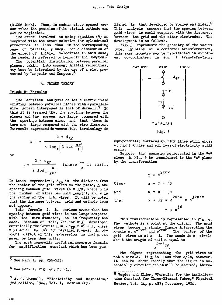
Vacuum Tube Design
(0.006 inch). Thus, in modern close -spaced vac-uum tubes the position of the virtual cathode cannot be neglected.
The error involved in using equation (9) ascompared with the exact solution for cylindricalstructures is less than in the correspondingcase of parallel planes. For a discussion ofthe effect of initial velocities in this casethe reader is referred to Langmuir and Compton.
A
The potential distribution between parallelplanes, taking into account initial velocities,may best be determined by the use of a plot pre-sented by Langmuir and Compton.6
B. TRIODE THEORY
Triode Mu Formulas
The earliest analysis of the electric fieldexisting between parallel planes with a parallel -wire screen interposed is that of Maxwel1.7 Inthis it is assumed that the spacings between theplanes and the screen are large compared withthe spacings between wires and that these inturn are large compared with the wire diameter.The result expressed in vacuum -tube terminology is
or
=
2 itdgp
a loge(2 sin 11)a
2 n dgp
aa loge
2nr
(where n r
ais small)
In these expressions, dgp is the distance fromthe center of the grid wires to the plate, a thespacing between grid wires (a = 1/n, where n isthe number of wires per unit length), and r isthe radius of the grid wires. It will be notedthat the distance between grid and cathode doesnot appear.
This formula is in serious error when thespacing between grid wires is not large comparedwith the wire diameter, as is frequently thecase. Because of this, Van der Bill developedempirically the formula µ = C dgp r n2 + 1, whereC is equal to 160 for parallel planes. An ob-vious defect of this expression is that µ cannever be less than unity.
The most generally useful and accurate formulafor amplification constant which has been pub -
5 See Ref. 1, pp. 252-255.
6 See Ref. 1, Fig. 42, p. 243.
7 J. C. Maxwell, "Electricity and Magnetism,"3rd edition, 1904, Vol. 1, Section 203. Review, Vol. 24, p. 683; December, 1924.
lished is that developed by Vogdes and Elder.8This analysis assumes that the spacing betweengrid wires is small compared with the distancesbetween the grid and the other electrodes. Thedevelopment is as follows.
Fig. 3 represents the geometry of the vacuumtube. By means of a conformal transformation,this same geometry may be represented in differ-ent co-ordinates. In such a transformation,
CATHODE
00
GRID
a dqp
+U.
0" W" PLANE
Fig. 3
equipotential surfaces and flux lines still crossat right angles and all laws of electricity stillapply.
Suppose the geometry represented in the "w"plane in Fig. 3 be transformed to the "z" planeby the transformation
Since
and
thene2nnu
x ej2nnv
= p eje
This transformation is represented in Fig. 4.The cathode is a point at the origin. The gridwires become a single figure intersecting thex-axis ate 4'nr and e271" The center of thegrid wires is at x = 1. The anode is a circleabout the origin of radius equal to
2nndgpe
The figure representing the grid wires isnot a circle. If r is less than a/2n, however,it can be shown readily that the figure is es-sentially circular and it will be assumed, there -
z = e2nnw
z = x + jy
w = u + jv
ANODE
8 Vogdes and Elder, "Formulas for the Amplifica-tion Constant for Three -Element Tubes," Physical
118
Thompson: Space -Current Flow in Vacuum -Tube Structures
fore, that such is the case. If the figure isa circle, its radius is
e2nnr - e-2nnr
2- sinh 2nnr
and its center is located at
e2nnr + e-2nnrx -
2- cosh 2nnr
In Fig. 3, if the anode were removed to
infinity and a potential applied to the grid,
the successive equipotential surfaces at greater
~Z~ PLANE
Fig. 4
distances from the grid would become more andmore nearly planes until, at distances severaltimes a, the surface could be regarded as essen-tially a plane. Therefore, under the limitationsof our assumptions concerning relative spacings,the anode plane may be considered to be theequipotential surface due to the field of thegrid alone. This is equivalent to saying that acircle of radius
2nndgpe - cosh 2nnr
drawn about the "center" of the grid wire inFig. 4 does not differ materially from a circleof radius
2nndgpe
drawn about the origin. The justification forthis assumption maybe checked by considering therather extreme case where nd = 0.50stnd nr =gp
0.03. Then2nndgp
equals 23.1 and cosh 2nnr equals 1.02.
The convenient result of these assumptionsis that a line charge placed at the "center" ofthe circular grid wire, Fig. 4, produces equi-potential surfaces at the surface of the gridwires and at the anode, since the charge on the
cathode located at minus infinity must be zero.Let us place a charge -Q at the "center" of
the grid wire. The potentials Ek, Eg, and Ea ofthe cathode, grid, and anode become
Ek = C + 2 Q log cosh 2nnr
Eg = C + 2 0, log sinh 2nnr
Ea = C + 2 Q 2nndgp
If the cathode potential be taken as zero,
Eg = 2Q log sinh 2nnr - 2Q log cosh 2nnr
= 2Q log tanh 2nnr
and
Ea = 2Q 2nndgp - 2Q log cosh 2nnr
Under these circumstances, the amplification con-stant may be defined as
whence
Ea= --Eg
log cosh 2nnr - 2nndgp
log tanh 2nnr
The assumptions made in this derivation in-
validate the expression for use with relativelyvery close spacings between electrodes. The sametype of analysis as that presented by Vogdes andElder may be made to give more rigorous results.Mr. Bernard Salzberg of the Radiotron Labora-tories has carried out such an analysis. It dif-fers from that just presented chiefly in that anadditional line charge is placed on the x-axis,Fig. 4, outside the anode at such a position as
to make the true anode cylinder an equipotentialsurface. Therefore, the anode may be allowed toapproach much more closely to the grid. This
leads to an expression accurate for cases wherethe spacing between anode and grid is small com-pared with the wire spacing, though not when thewire spacing is small compared with the wire di-ameter. Mr. Salzberg's expression is
1-1 -
-
log cosh 2nnr -
log tanh 2nnr -
2nndgp
log(1 - e-4nndgp x cosh2 2nnr)
* Ref. 11-12-13-14, asterisk.
119
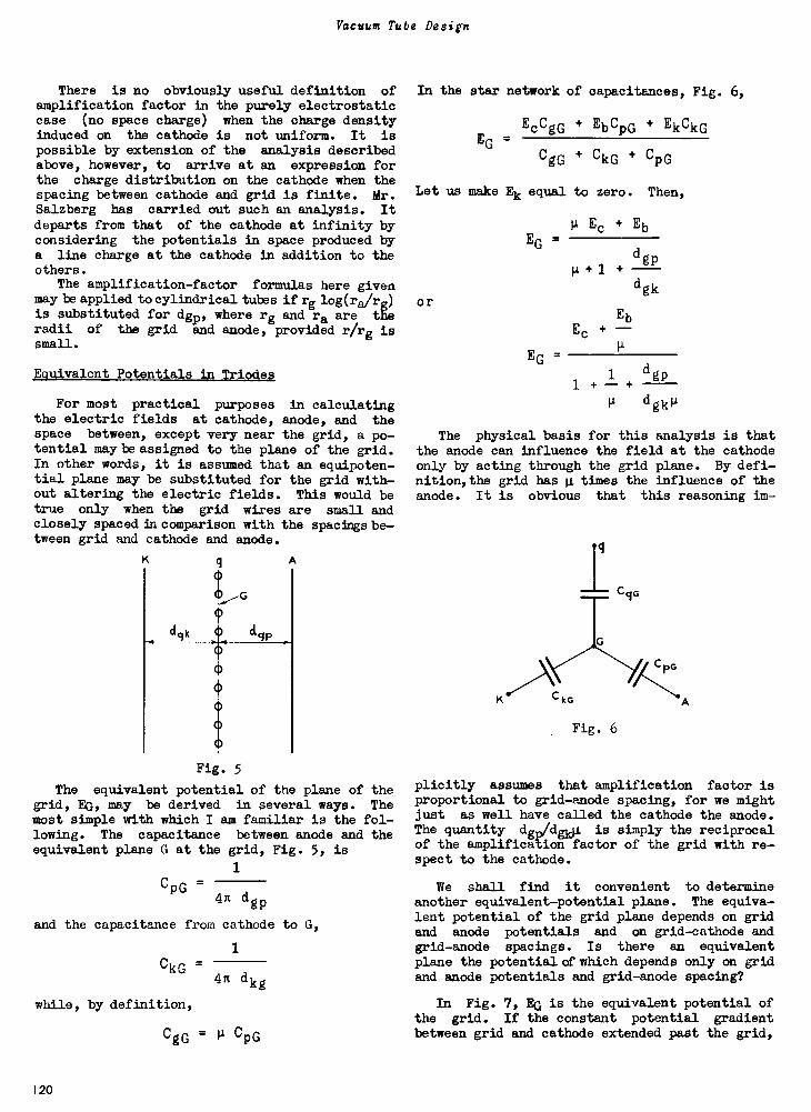
Vacuum Tube Design
There is no obviously useful definition ofamplification factor in the purely electrostaticcase (no space charge) when the charge densityinduced on the cathode is not uniform. It ispossible by extension of the analysis describedabove, however, to arrive at an expression forthe charge distribution on the cathode when thespacing between cathode and grid is finite. Mr.Salzberg has carried out such an analysis. Itdeparts from that of the cathode at infinity byconsidering the potentials in space produced bya line charge at the cathode in addition to theothers.
The amplification -factor formulas here givenmay be applied to cylindrical tubes if rg log(ra/rg)
is substituted for dgp, where rg and ra are theradii of the grid and anode, provided r/rg issmall.
Equivalent Potentials in Triodes
For most practical purposes in calculatingthe electric fields at cathode, anode, and thespace between, except very near the grid, a po-tential maybe assigned to the plane of the grid.In other words, it is assumed that an equipoten-tial plane may be substituted for the grid with-out altering the electric fields. This would betrue only when the grid wires are small andclosely spaced in comparison with the spacings be-tween grid and cathode and anode.
Fig. 5
The equivalent potential of the plane of thegrid, EG, may be derived in several ways. Themost simple with which I am familiar is the fol-lowing. The capacitance between anode and theequivalent plane G at the grid, Fig. 5, is
CpG1
4n dgp
and the capacitance from cathode to G,
1
CkG
while, by definition,
4n dkg
CgG = µ CpG
In the star network of capacitances, Fig. 6,
EGgcCgG EbCpG EkCkG
CgG CkG CpG
Let us make Ek equal to zero.
or
EG
EG
Ec
Then,
Eb
dgP
d g k
Eb
Ec
The physical basisthe anode can influenceonly by acting throughnition,the grid has µ tanode. It is obvious
K CkG
dgp
dgki.L
for this analysis is thatthe field at the cathode
the grid plane. By defi-imes the influence of thethat this reasoning im-
C qG
Fig. 6
plicitly assumes that amplification factor isproportional to grid -anode spacing, for we mightjust as well have called the cathode the anode.The quantity dgridgiiµ is simply the reciprocalof the amplification factor of the grid with re-spect to the cathode.
We shall find it convenient to determineanother equivalent -potential plane. The equiva-lent potential of the grid plane depends on gridand anode potentials and on grid -cathode andgrid -anode spacings. Is there an equivalentplane the potential of which depends only on gridand anode potentials and grid -anode spacing?
In Fig. 7, EG is the equivalent potential ofthe grid. If the constant potential gradientbetween grid and cathode extended past the grid,
120
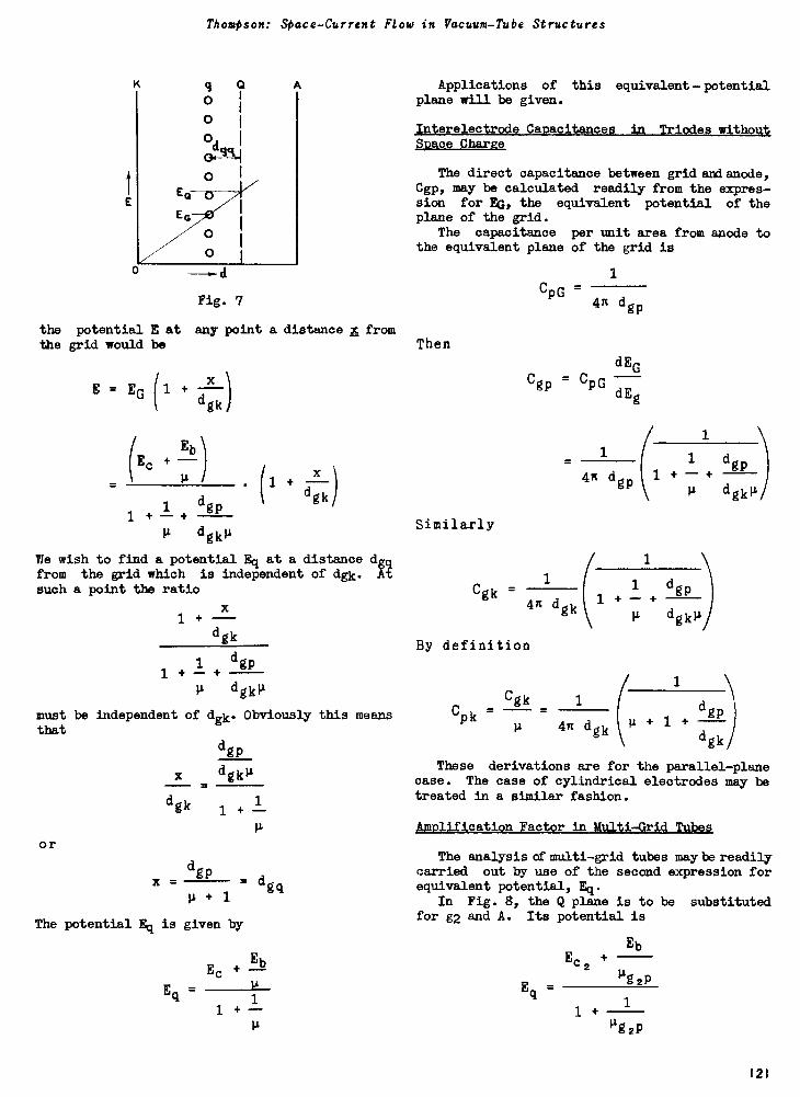
Thompson: Space -Current Flow in Vacuum -Tube Structures
K
E
9 ?0
0O I
a
O 1
O
A
-mod
Fig. 7
the potential E at any point a distance x fromthe grid would be
E = EG (1 +
(EcEbEb
dgk
1 + - +1
dgp
dgo
(1 +x
dgk
We wish to find a potential Eq at a distance dgqfrom the grid which is independent of dgk. Atsuch a point the ratio
1x
dgk
1+
dgp
p dgkp
must be independent of dgk. Obviously this meansthat
or
1 +
dgp
x clod./
dgk
dgp
11 4'
1 +1
q.
1
- dg
The potential Eq is given by
Eq =Ec
1
Eb
1
Applications of thisplane will be given.
Interelectrode CapacitancesSpace Charge
equivalent - potential
in Triodes without
The direct capacitance between grid and anode,Cgp, may be calculated readily from the expres-sion for EG, the equivalent potential of theplane of the grid.
The capacitance per unit area from anode tothe equivalent plane of the grid is
Then
Similarly
CpG1
4n dgp
CgpCPG dEg
1Cgk -
4n dgk
By definition
Cpk -Cgk
dEG
1
4n dgp
1
1
1 +
1 dgP- +
p dgkp/
1
1
+
dgP
dgkpl
1
4n dgk \4 1dgp
dgk
These derivations are for the parallel -planecase. The case of cylindrical electrodes may betreated in a similar fashion.
Amplification Factor in Multi -Grid Tubes
The analysis of multi -grid tubes maybe readilycarried out by use of the second expression forequivalent potential, Eq.
In Fig. 8, the Q plane is to be substitutedfor g2 and A. Its potential is
Eq
EbE +c2
Pg2P
1
Pg2P1
121
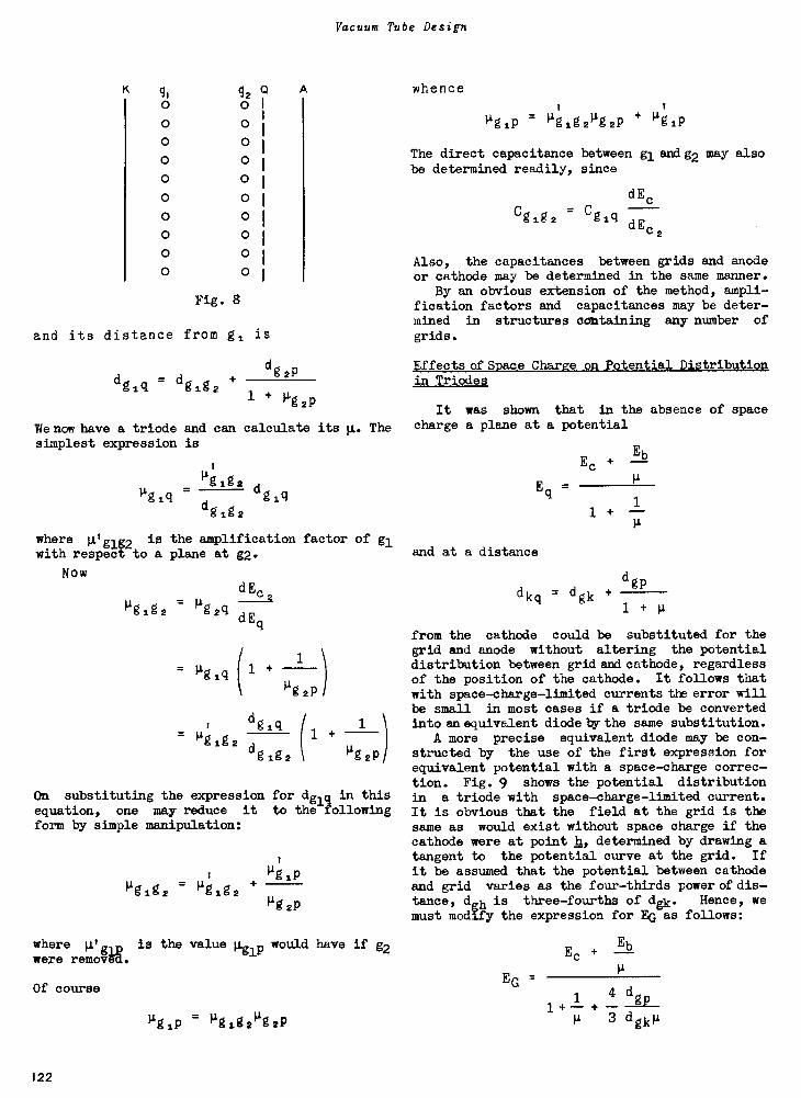
Vacuum Tube Design
K
o
0
0
0
0
0
0
0
q20 I
0 I
0
A whence
= liglg2N2p Nip
I
0 1
The direct capacitance between glanig2 may alsobe determined readily, since
0 1
0 1dEc
0 1
Co0olo2 = Cgig
dE01 C2
0 1
Also, the capacitances between grids and anode0 1 or cathode may be determined in the same manner.
Fig. 8
and its distance from g, is
ddglq = dgig2 g2Pin Triodes
1 + µg
We now have a triode and can calculate its µ. Thesimplest expression is
By an obvious extension of the method, ampli-fication factors and capacitances may be deter-mined in structures containing any number of
grids.
- Pg1g2 dgig
dg1g2
where µIgig2 is the amplification factor of glwith respect to a plane at g2. and at a distance
Effects of Space Charge on Potential Distribution
It was shown that in the absence of spacecharge a plane at a potential
Now
1-11 ig
dEc= p s
g2c1 dEq
(1 1
µg 2P
dgiq
(1 +
1
= Pgig2dgigs
N2131
On substituting the expression for dg15 in thisequation, one may reduce it to the followingform by simple manipulation:
Agig2Ago
= Nig2µg 2P
where Wgir, is the value µgip would have if g2were remove.
Of course
Ago = Agig2N2p
Eq =
Ec + Eb
A
1 +1-A
dkq = dgk +dgP
1 +
from the cathode could be substituted for thegrid and anode without altering the potentialdistribution between grid and cathode, regardlessof the position of the cathode. It follows thatwith space -charge -limited currents the error willbe small in most cases if a triode be convertedinto an equivalent diode by the same substitution.
A more precise equivalent diode may be con-structed by the use of the first expression forequivalent potential with a space -charge correc-tion. Fig. 9 shows the potential distributionin a triode with space -charge -limited current.
It is obvious that the field at the grid is thesame as would exist without space charge if thecathode were at point h, determined by drawing atangent to the potential curve at the grid. Ifit be assumed that the potential between cathodeand grid varies as the four -thirds power of dis-tance, dah is three -fourths of dgk. Hence, wemust modify the expression for EG as follows:
EG
Ec +Eb
1 4 dgp1 + - +
µ 3 dgkµ
122

Themtson: Sfiace -Current Flow in Vacuum -Tube Structures
Fig. 9
The analysis of the current -voltage relation-ship of a triode may be made directly from thediode case by the use of this equivalent -diodeexpression. If in the equivalent diode the spacecurrent
Ib = f(EG)
the cathode current (equal to the plate currentwith negative grid) is given directly. The trans -conductance, gm, is found by tAking the deriva-tive of f(EG) with respect to Ec. The plate con-ductance, 1/ip is found by taking the derivativeof f(EG) with respect to Eb.
Electron Transit Time In Negative -Grid Triodes
The electron transit time in any electrodestructure may be calculated readily if the po-tential distribution is known. In general
dx m zdxt = - = -f V 2e Et
The calculation of transit time in the absenceof space charge is obvious. In a parallel -planediode with space -charge -limited current, thetransit time from cathode to anode may be calcu-lated if it be assumed that
whence
t
X 3
E Eb (-dkp
2
111 dkp= -2 e Eb
3 dkp
2e ET
dkp= 5.05 x 10
E223
where t is in seconds, dkp in centimeters, andEb in volts. In other words, the electron takesthree times as long to pass from cathode to anodeas if it had traveled at the final velocity theentire distance, and half again as long as if ithad been uniformly accelerated.
The cylindrical analysis is not so simple butmay be carried out as presented by W. R. Ferris.9
In the case of electron transits between gridand anode, the integration is carried out withthe initial velocity of the electron correspond-ing to the equivalent potential of the grid.
9 W. R. Ferris, "Input Resistance of Vacuum TubesesUltra-High-Frequency Amplifiers,"Proc. I.R.E.,Vol. 24, p. 82; January, 1936.
123
Lecture 15*
ELECTRON OPTICS
Part I . DETERMINATION OF ELECTRON TRAJECTORIES
V. K. Zworykin and G. A. Morton
INTRODUCTION
The term "electron optics" will be used to
describe that class of problems which deals withthe determination of electron trajectories. Theexpression originated as a consequence of theclose analogy between optical arrangements andthe corresponding electronic systems. It wasfound that this analogy not only had fundamentalmathematical significance, but, in many cases,could be extended to practical devices. For ex-ample, it is possible to construct electronlenses which are capable of imaging an electronsource. In many instances not only is the be-havior of the two types of systems the same, butalso many of the mathematical methods of opticscan be applied to the corresponding electronproblem. There are, it is true, many systemswhich in no way resemble those of conventionaloptics. However, there is a continuous tran-sition between these and such as have a closeoptical analogue. Therefore, any attempt to
subdivide the field on this basis results onlyin confusion.
The importance of electron optics is becomingincreasingly apparent with the advance of elec-tronics. For example, in the early vacuum tubesused in radio work little attention was paid tothe exact paths of the electrons between thecathode and the plate. Recently, very real im-provement in efficiency and performance has beenachieved by the application of electron opticsto tube design. In the design of the newer de-vices, such as the secondary -emission multiplier,the electron gun used in television tubes, andthe image tubes, electron optics is essential.
The design problem usually encountered is onein which the two termini of the electron paths arespecified and it is required to determine anelectrode and magnetic coil configuration thatwill satisfy this demand. Unfortunately, a di-rect solution is still a good deal beyond ourpresent mathematical means. It is not possible,except in very special cases, to determine froma given electron path the shape and potentialsof the electrodes required to produce this path.In order to solve the above problem, it is nec-essary to assume an electrode configuration andthen determine the resulting electron path. Ifthis is not the required path the electrodes arechanged and the trajectories recalculated. Usu-ally this process does not have to be repeated
* This lecture contains the same material asChapter 3 of the book TELEVISION by Zworykin andMorton. Used by permission of John Wiley andSons.
very many times before the correct solution isreached, as the previously determined paths indi-cate the nature of the changes that must be made.
Restating the problem in the only form inwhich a solution is possible, it becomes: Givenan electrode configuration and the potentialsapplied, determine the electron paths in the re-sulting potential field. Even this problem hasno general solution, and often can be solved onlyby resorting to elaborate mathematical approxi-mations, or to the use of mechanical and graphi-cal methods. The solution can be divided intotwo distinct parts; namely, the determination ofthe potential field produced by the electrodes,and the calculation of the electron trajectoriesin this field. Essentially the same procedureis used when the electrons are guided by magneticfields.
THE LAPLACE EQUATION
To determine the potential field produced bya given set of electrodes, it is necessary tosolve the Laplace differential equation:
asp astp
= 0axe aye
(1)
with boundary conditions corresponding to theshapes and potentials of the electrodes. The so-lution of this equation gives the potential as afunction of the coordinates, that is:
T (x017,z)
The electrostatic field can be found from thispotential by differentiation with respect to thecoordinates. Thus:
Ex = - cp(x,y,z)ax
E -Y
Hz
a- q)(x,y,z)ay
- -a=az
From the original Laplace equation, which is sat-isfied by the potential function, it will be seenthat the field must satisfy the differentialequation:
aEx BE aEz- + + - = 0ax ay az
124
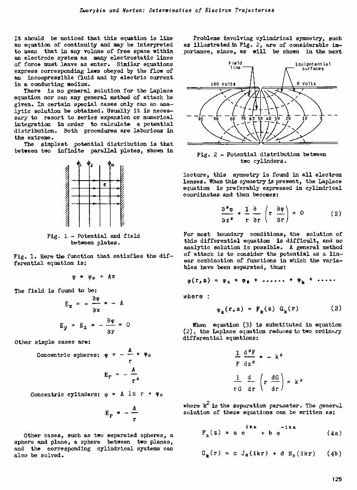
Zworykin and Morton: Determination of Electron Trajectories
It should be noticed that this equation is likean equation of continuity and may be interpretedto mean that in any volume of free apace withinan electrode system as many electrostatic linesof force must leave as enter. Similar equationsexpress corresponding laws obeyed by the flow ofan incompressible fluid and by electric currentin a conducting medium.
There is no general solution for the Laplaceequation nor can any general method of attack begiven. In certain special cases only can an ana-lytic solution be obtained. 11311)01y it is neces-sary to resort to series expansion or numericalintegration in order to calculate a potentialdistribution. Both procedures are laborious inthe extreme.
The simplest potential distribution is thatbetween two infinite parallel plates, shown in
Fig. 1 - Potential and fieldbetween plates.
Fig. 1. Here the function that satisfies the dif-ferential equation is:
= Ax
The field is found to be:
By
Ex = = Aax
ByEY = Ez = - =
Other simple cases are:
Concentric spheres:
By
(I) ,
Er
0
A-+r
r2
To
Concentric cylinders: p= A ln r+ To
AEr = -
r
Other cases, such as two separated spheres, asphere and plane, a sphere between two planes,and the corresponding cylindrical systems canalso be solved.
Problems involving cylindrical symmetry, suchas illustrated in Fig. 2, are of considerable im-portance, since, as will be shown in the next
field1 ine
Equipotent ialsurfaces
100 Volts 0 Volts
95 90 80 70 605050 30 20 10
Fig. 2 - Potential distribution betweentwo cylinders.
lecture, this symmetry is found in all electronlenses. When this symmetry is present, the Laplaceequation is preferably expressed in cylindricalcoordinates and then becomes:
B2y l a (r
awlBz r Br Br(2)
For most boundary conditions, the solution ofthis differential equation is difficult, and noanalytic solution is possible. A general methodof attack is to consider the potential as a lin-ear combination of functions in which the varia-bles have been separated, thus:
p(r,z) = pl Ts cPk
where :
Tk(r,z) = Fk(z) Gk(r) (3)
When equation (3) is substituted in equation(2), the Laplace equation reduces to two ordinarydifferential equations:
1 d2F= - k
F dz2
2
1 dr
dG)= k2
rG dr dr
where k2 is the separation parameter. The generalsolution of these equations can be written as:
ikzFk(z) = a e + b e (4a)
Gk(r) = c Jo(ikr) + d No(ikr) (4b)
125
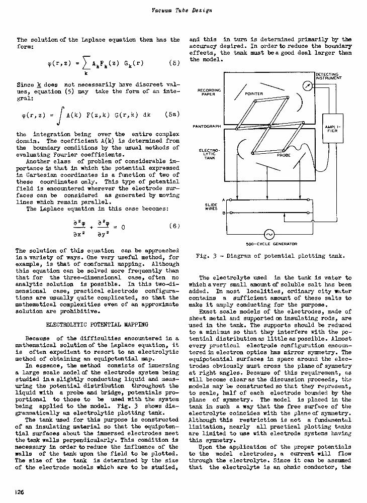
Vacuum Tube Design
axe
The solution of the Laplace equation then has theform:
p(r,z) = Fk(z) Gk(r) (5)
Since k does not necessarily have discreet val-ues, equation (5) may take the form of an inte-gral:
fcp(r,z) = A(k) F(z,k) G(r,k) dk (5a)
the integration being over the entire complexdomain. The coefficient A(k) is determined fromthe boundary conditions by the usual methods ofevaluating Fourier coefficients.
Another class of problem of considerable im-portance is that in which the potential expressedin Cartesian coordinates is a function of two ofthese coordinates only. This type of potentialfield is encountered wherever the electrode sur-faces can be considered as generated by movinglines which remain parallel.
The Laplace equation in this case becomes:
a2cp B2cp
aye( 6 )
The solution of this equation can be approachedina variety of ways. One very useful method, forexample, is that of conformal mapping. Althoughthis equation can be solved more frequently thanthat for the three-dimensional case, often noanalytic solution is possible. In this two-di-mensional case, practical electrode configura-tions are usually quite complicated, so that themathematical complexities even of an approximatesolution are prohibitive.
RLECTROLYTIC POTENTIAL MAPPING
Because of the difficulties encountered in amathematical solution of the Laplace equation, itis often expedient to resort to an electrolyticmethod of obtaining an equipotential map.
In essence, the method consists of immersinga large scale model of the electrode system beingstudied ina slightly conducting liquid and meas-uring the potential distribution throughout theliquid with a probe and bridge, potentials pro-portional to those to be used with the systembeing applied to the model. Fig. 3 shows dia-grammatically an electrolytic plotting tank.
The tank used for this purpose is constructedof an insulating material so that the equipoten-tial surfaces about the immersed electrodes meetthe tank walls perpendicularly. This condition isnecessary in order to reduce the influence of thewalls of the tank upon the field to be plotted.The size of the tank is determined by the sizeof the electrode models which are to be studied,
and this in turn is determined primarily by theaccuracy desired. In order to reduce the boundaryeffects, the tank must boa good deal larger thanthe model.
RECORDINGPAPER
PANTOGRAPH
ELECTRO-LYTICTANK
A-0SLIDEW IRES
B
500. CYCLE GENERATOR
DETECTINGINSTRUMENT
AMPLI-FIER
Fig. 3 - Diagram of potential plotting tank.
The electrolyte used in the tank is water towhich aver -y small amountcf soluble salt has beenadded. In most localities, ordinary city watercontains a sufficient amount of these salts tomake it amply conducting for the purpose.
Exact scale models of the electrodes, made ofsheet metal and supported on insulating rods, areused in the tank. The supports should be reducedto a minimum so that they interfere with the po-tential distribution as little as possible. Almostevery practical electrode configuration encoun-tered in electron optics has mirror symmetry. Theequipotential surfaces in space around the elec-trodes obviously must cross the plane of symmetryat right angles. Because of this requirement, aswill become clear as the discussion proceeds, themodels may be constructed so that they represent,to scale, half of each electrode bounded by theplane of symmetry. The model is placed in thetank in such a way that the free surface of theelectrolyte coincides with the plane of symmetry.Although this restriction is not a fundamentallimitation, nearly all practical plotting tanksare limited to use with electrode systems havingthis symmetry.
Upon the application of the proper potentialsto the model electrodes, a current will flowthrough the electrolyte. Since it can be assumedthat the electrolyte is an ohmic conductor, the
126
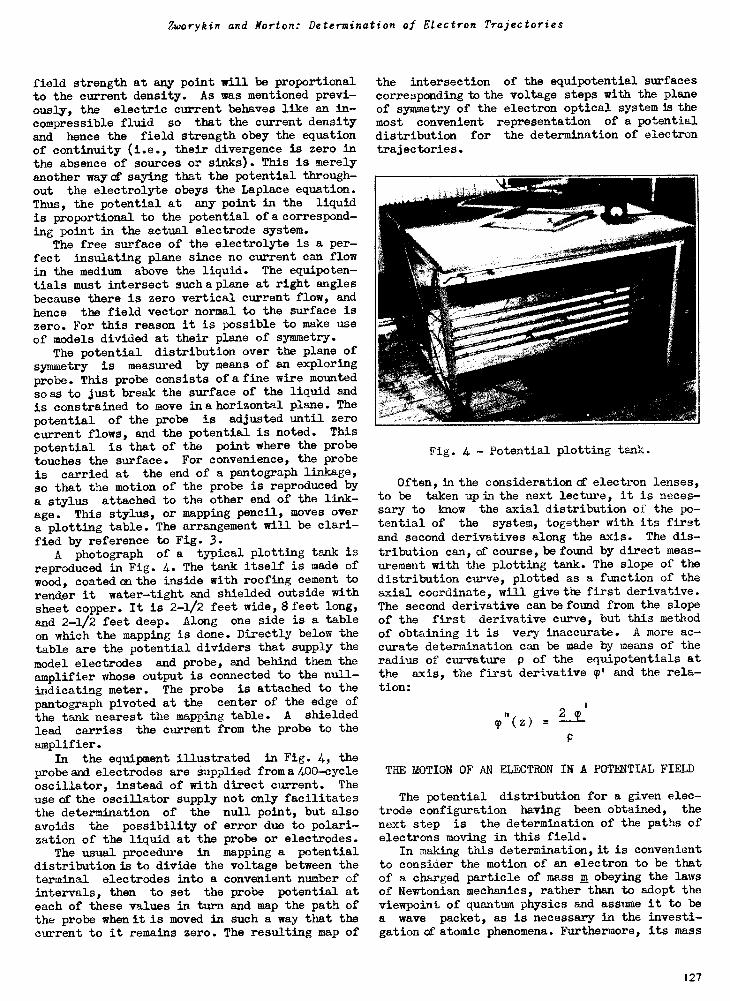
Zworykin and Morton: Determination of Electron Trajectories
field strength at any point will be proportionalto the current density. As was mentioned previ-ously, the electric current behaves like an in-compressible fluid so that the current densityand hence the field strength obey the equationof continuity (i.e., their divergence is zero inthe absence of sources or sinks). This is merelyanother waycf saying that the potential through-out the electrolyte obeys the Laplace equation.Thus, the potential at any point in the liquidis proportional to the potential of a correspond-ing point in the actual electrode system.
The free surface of the electrolyte is a per-fect insulating plane since no current can flowin the medium above the liquid. The equipoten-tials must intersect such a plane at right anglesbecause there is zero vertical current flow, and
hence the field vector normal to the surface iszero. For this reason it is possible to make useof models divided at their plane of symmetry.
The potential distribution over the plane of
symmetry is measured by means of an exploringprobe. This probe consists of a fine wire mountedso as to just break the surface of the liquid andis constrained to move inahorizontal plane. Thepotential of the probe is adjusted until zero
current flows, and the potential is noted. This
potential is that of the point where the probe
touches the surface. For convenience, the probe
is carried at the end of a pantograph linkage,so that the motion of the probe is reproduced by
a stylus attached to the other end of the link-
age. This stylus, or mapping pencil, moves overa plotting table. The arrangement will be clari-
fied by reference to Fig. 3.A photograph of a typical plotting tank is
reproduced in Fig. 4. The tank itself is made ofwood, coated on the inside with roofing cement to
render it water -tight and shielded outside withsheet copper. It is 2-1/2 feet wide, 8feet long,
and 2-1/2 feet deep. Along one side is a table
on which the mapping is done. Directly below the
table are the potential dividers that supply the
model electrodes and probe, and behind them theamplifier whose output is connected to the null -
indicating meter. The probe is attached to the
pantograph pivoted at the center of the edge of
the tank nearest the mapping table. A shielded
lead carries the current from the probe to the
amplifier.
In the equipment illustrated in Fig. 4, theprobe and electrodes are supplied froma4.00-cycleoscillator, instead of with direct current. The
use of the oscillator supply not only facilitatesthe determination of the null point, but also
avoids the possibility of error due to polari-zation of the liquid at the probe or electrodes.
The usual procedure in mapping a potentialdistribution is to divide the voltage between theterminal electrodes into a convenient number ofintervals, then to set the probe potential ateach of these values in turn and map the path ofthe probe when it is moved in such a way that thecurrent to it remains zero. The resulting map of
the intersection of the equipotential surfacescorresponding to the voltage steps with the planeof symmetry of the electron optical system is themost convenient representation of a potential
distribution for the determination of electron
trajectories.
Fig. 4 - Potential plotting tank.
Often, in the consideration of electron lenses,to be taken up in the next lecture, it is neces-sary to know the axial distribution of the po-tential of the system, together with its firstand second derivatives along the axis. The dis-
tribution can, of course, be found by direct meas-urement with the plotting tank. The slope of thedistribution curve, plotted as a function of theaxial coordinate, will give the first derivative.The second derivative can be found from the slope
of the first derivative curve, but this method
of obtaining it is very inaccurate. A more ac-curate determination can be made by means of theradius of curvature p of the equipotentials at
the axis, the first derivative pt and the rela-tion:
2 q)
THE MOTION OF AN ELECTRON IN A POTENTIAL FIELD
The potential distribution for a given elec-trode configuration having been obtained, the
next step is the determination of the paths ofelectrons moving in this field.
In making this determination, it is convenientto consider the motion of an electron to be thatof a charged particle of mass m obeying the lawsof Newtonian mechanics, rather than to adopt theviewpoint of quantum physics and assume it to bea wave packet, as is necessary in the investi-gation of atomic phenomena. Furthermore, its mass
127
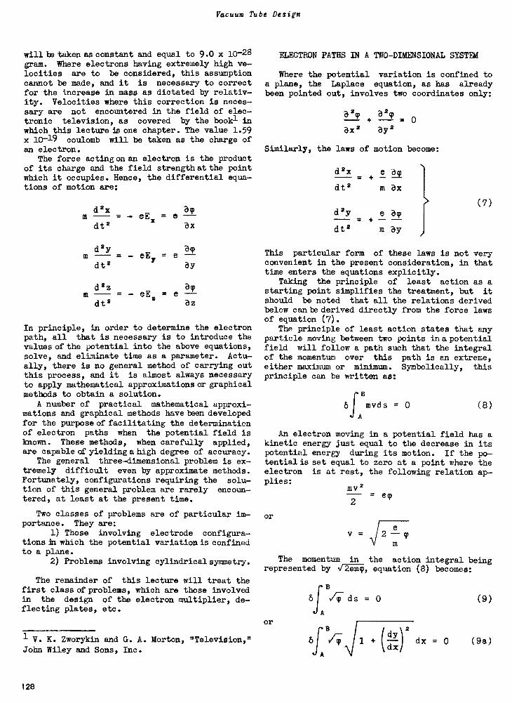
Vacuum Tube Design
will be taken as constant and equal to 9.0 x 10⁻²⁸gram. Where electrons having extremely high ve-locities are to be considered, this assumptioncannot be made, and it is necessary to correctfor the increase in mass as dictated by relativ-ity. Velocities where this correction is neces-sary are not encountered in the field of elec-tronic television, as covered by the bookl inwhich this lecture is one chapter. The value 1.59x 10⁻¹⁹ coulomb will be taken as the charge ofan electron.
The force acting on an electron is the productof its charge and the field strength at the pointwhich it occupies. Hence, the differential equa-tions of motion are:
d 2m
x= - eEz = eat
dt2 ax
d2y -dt2
= - eE = e"am
ay
dgz(1)- = - = ea
dt2 az
In principle, in order to determine the electronpath, all that is necessary is to introduce thevalues of the potential into the above equations,solve, and eliminate time as a parameter. Actu-ally, there is no general method of carrying outthis process, and it is almost always necessaryto apply mathematical approximations or graphicalmethods to obtain a solution.
A number of practical mathematical approxi-mations and graphical methods have been developedfor the purpose of facilitating the determinationof electron paths when the potential field isknown. These methods, when carefully applied,are capable of yielding a high degree of accuracy.
The general three-dimensional problem is ex-tremely difficult even by approximate methods.Fortunately, configurations requiring the solu-tion of this general problem are rarely encoun-tered, at least at the present time.
Two classes of problems are of particular im-portance. They are:
1) Those involving electrode configura-tionsin which the potential variation is confinedto a plane.
2) Problems involving cylindrical symmetry.
The remainder of this lecture will treat thefirst class of problems, which are those involvedin the design of the electron multiplier, de-flecting plates, etc.
1 V. K. Zworykin and G. A. Morton, "Television,"
John Wiley and Sons, Inc.
ELECTRON PATHS IN A TWO-DIMENSIONAL SYSTEM
Where thea plane, thebeen pointed
Similarly,
potential variation is confined toLaplace equation, as has alreadyout, involves two coordinates only:
any
axea2T = o
2
the laws of motion become:
d 2x e
m axdt2
d2y+
e- -m ay
(7)
dt2
This particular form of these laws is not veryconvenient in the present consideration, in thattime enters the equations explicitly.
Taking the principle of least action as astarting point simplifies the treatment, but itshould be noted that all the relations derivedbelow can be derived directly from the force lawsof equation (7).
The principle of least action states that anyparticle moving between two points in a potentialfield will follow a path such that the integralof the momentum over this path is an extreme,either maximum or minimum. Symbolically, thisprinciple can be written as:
f6 muds = 0A
(8)
An electron moving in a potential field has akinetic energy just equal to the decrease in itspotential energy during its motion. If the po-tential is set equal to zero at a point where theelectron is at rest, the following relation ap-plies:
M V2
or
2ecp
v = /2 -cp
The momentum in the action integral beingrepresented by f, equation (8) becomes:
or
of14-p- d s = 0
A
(9)
2
C121 ) dx = 0dx
(9a)
128
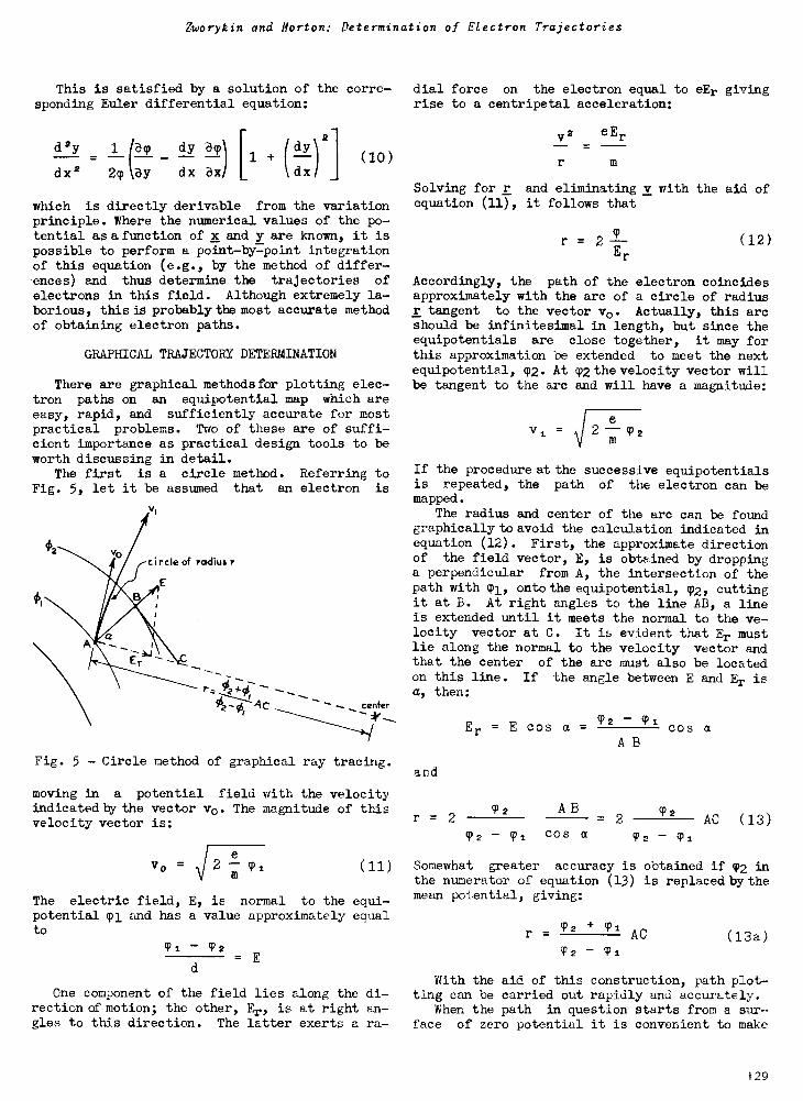
Zworykin and Morton: Determination of Electron Trajectories
This is satisfied by a solution of the corre-sponding Euler differential equation:
d2y 1 dy
dx2 2(p
(acp
ay dx
E1 ( dy)(10 )
dx
which is directly derivable from the variationprinciple. Where the numerical values of the po-tential as a function of x and y are known, it ispossible to perform a point -by -point integrationof this equation (e.g., by the method of differ-ences) and thus determine the trajectories of
electrons in this field. Although extremely la-borious, this i5 probably the most accurate methodof obtaining electron paths.
GRAPHICAL TRAJECTORY DETERMINATION
There are graphical methods for plotting elec-tron paths on an equipotential map which areeasy, rapid, and sufficiently accurate for mostpractical problems. Two of these are of suffi-cient importance as practical design tools to beworth discussing in detail.
The first is a circle method. Referring toFig. 5, let it be assumed that an electron is
v,
c i rcie of radius r
E
-Cr".------42-561 center
Fig. 5 - Circle method of graphical ray tracing.
moving in a potential field with the velocityindicated by the vector vo. The magnitude of thisvelocity vector is:
evo = 2 ; Ti
The electric field, E, is normal to the equi-potential 91 and has a value approximately equalto
cP 1 - (1) 2- E
d
One component of the field lies along the di-rection of motion; the other, Er, is at right an-gles to this direction. The latter exerts a ra-
dial force on the electron equal to eEr givingrise to a centripetal acceleration:
V2 eEr
r in
Solving for r and eliminating v with the aid ofequation (11), it follows that
r = 2
E
9)
r
(12)
Accordingly, the path of the electron coincidesapproximately with the arc of a circle of radiusr tangent to the vector vo. Actually, this arcshould be infinitesimal in length, but since theequipotentials are close together, it may forthis approximation be extended to meet the nextequipotential, P2. At 92 the velocity vector willbe tangent to the arc and will have a magnitude:
v =m 2
If the procedure at the successive equipotentialsis repeated, the path of the electron can bemapped.
The radius and center of the arc can be foundgraphically to avoid the calculation indicated inequation (12). First, the approximate directionof the field vector, E, is obtained by droppinga perpendicular from A, the intersection of thepath with 91, onto the equipotential, (p2, cuttingit at B. At right angles to the line AB, a lineis extended until it meets the normal to the ve-locity vector at C. It is evident that Er mustlie along the normal to the velocity vector andthat the center of the arc must also be locatedon this line. If the angle between E and Er isa, then:
and
Er = E cos a - (P2 cos aA B
(I) 2 ABr = 2
992 cos a
ci) 2- 2 AC (13)
P2 - Ti
Somewhat greater accuracy is obtained if 92 inthe numerator of equation (13) is replaced by themean potential, giving:
r P2 + (P1AC
9)2 - (I)
(13a)
With the aid of this construction, path plot-ting can be carried out rapidly and accurately.
When the path in question starts from a sur-face of zero potential it is convenient to make
129
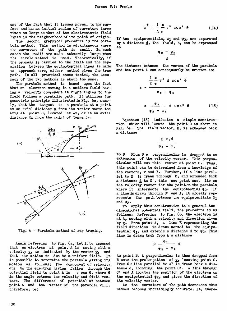
Vacuum Tube Design
use of the fact that it issues normal to the sur-face and has an initial radius of curvature threetimes as large as that of the electrostatic fieldlines in the neighborhood of its point of origin.
The second graphical procedure is the para-bola method. This method is advantageous wherethe curvature of the path is small. In suchcases the radii are made awkwardly large whenthe circle method is used. Theoretically, ifthe process is carried to the limit and the sep-aration between the equipotential lines is madeto approach zero, either method gives the truepath. In all practical cases tested, the accu-racy of the two methods is about the same.
The parabola method is based upon the factthat an electron moving in a uniform field hav-ing a velocity component at right angles to thefield follows a parabolic path. It utilizes thegeometric principle illustrated in Fig. 6a, name-ly, that the tangent to a parabola at a pointat an axial distance x from its vertex meets theaxis at point C, located at -x, or at an axialdistance 2x from the point of tangency.
(a)
24)1d
02-01 AI I
I
V
1.4114--x
Fig. 6 - Parabola method of ray tracing.
Again referring to Fig. 6a, let it be assumedthat an electron at point A is moving with avelocity v, as indicated by the vector v, andthat its motion is due to a uniform field. Itis possible to determine the parabola giving itsmotion as follows: The component of velocitydue to the electron having fallen through thepotential field to point A is v cos 8, where 8is the angle between the velocity and field vec-tors. The difference of potential p* betweenpoint A and the vertex of the parabola will,therefore, be:
* 1 mcp = - - v - cos 2 8
2 e(14)
If two equipotentials, Ti and P2, are separatedby a distance d, the field, E, can be expressedas
s - Tid
The distance between the vertex of the parabolaand the point A can consequently be written as:
1-m V2 d cosy e
2 e
s - Pi
(Pi d cos' e'P2 - (P1
(15)
Equation (15) indicates a simple construc-tion which will locate the point C as shown inFig. 6a. The field vector, E, is extended backa distance
2 cp id
- (P1
to B. From B a perpendicular is dropped to anextension of the velocity vector. This perpen-dicular will cut this vector at point C. Thus,
this point can be determined from a knowledge ofthe vectors, v and E. Further, if a line paral-lel to E is drawn through C, and extended backa distance d to C', this new point must lie onthe velocity vector for the point on the parabolawhere it intersects the equipotential 92. If
a line is drawn through CI and A, it closely rep-resents the path between the equipotentialsand 92.
To apply this construction to a general two-dimensional potential field, the procedure is asfollows: Referring to Fig. 6b, the electron isat A, moving with a velocity and direction givenby v. From point A, a line E representing thefield direction is drawn normal to the equipo-tential pi, and extends a distance d to T2. Thisline is drawn back from A a distance
'17
2 d
Ts - Ti
to point B. A perpendicular is then dropped fromB onto the prolongation of v, locating point C.From C aline parallel to AB is drawn back a dis-tance d, locating the point C'. A line throughC' and A locates the position of the electron onthe equipotential T2, and gives the direction ofits velocity vector.
As the curvature of the path decreases thismethod becomes increasingly accurate. It, there -
130
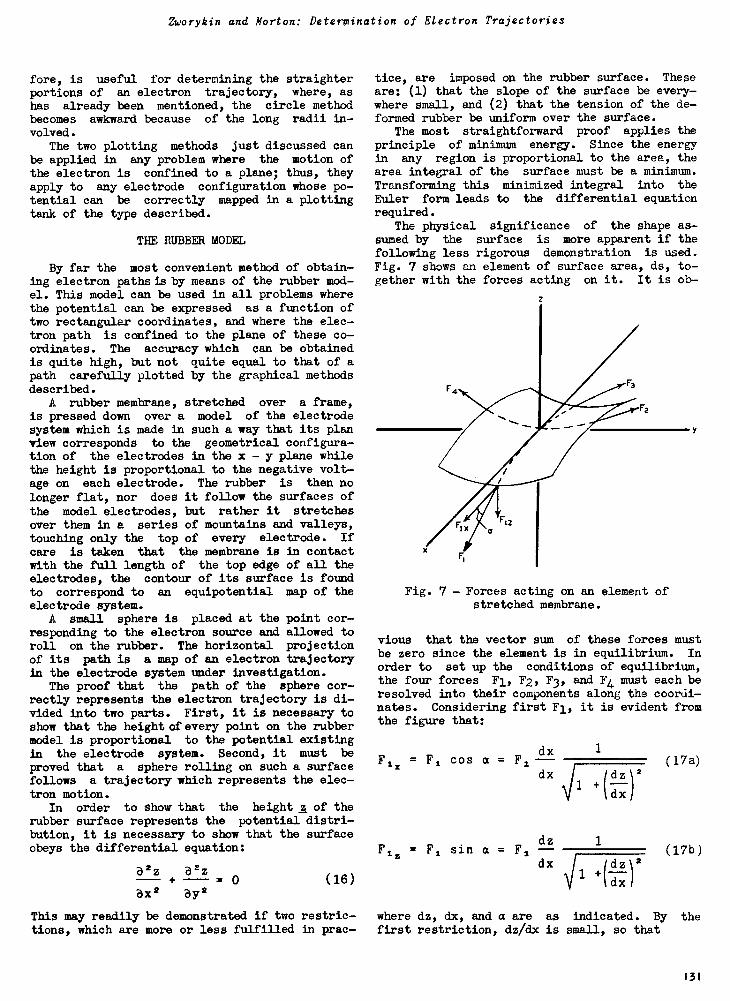
Zworykin and Morton: Determination of Electron Trajectories
fore, is useful for determining the straighterportions of an electron trajectory, where, ashas already been mentioned, the circle methodbecomes awkward because of the long radii in-volved.
The two plotting methods just discussed canbe applied in any problem where the motion ofthe electron is confined to a plane; thus, theyapply to any electrode configuration whose po-tential can be correctly mapped in a plottingtank of the type described.
THE RUBBER MODEL
By far the most convenient method of obtain-ing electron paths is by means of the rubber mod-el. This model can be used in all problems wherethe potential can be expressed as a function oftwo rectangular coordinates, and where the elec-tron path is confined to the plane of these co-ordinates. The accuracy which can be obtainedis quite high, but not quite equal to that of apath carefully plotted by the graphical methodsdescribed.
A rubber membrane, stretched over a frame,
is pressed down over a model of the electrodesystem which is made in such a way that its planview corresponds to the geometrical configura-tion of the electrodes in the x - y plane whilethe height is proportional to the negative volt-age on each electrode. The rubber is then no
longer flat, nor does it follow the surfaces of
the model electrodes, but rather it stretchesover them in a series of mountains and valleys,touching only the top of every electrode. If
care is taken that the membrane is in contactwith the full length of the top edge of all theelectrodes, the contour of its surface is foundto correspond to an equipotential map of theelectrode system.
A small sphere is placed at the point cor-responding to the electron source and allowed toroll on the rubber. The horizontal projectionof its path is a map of an electron trajectoryin the electrode system under investigation.
The proof that the path of the sphere cor-rectly represents the electron trajectory is di-vided into two parts. First, it is necessary toshow that the height of every point on the rubbermodel is proportional to the potential existingin the electrode system. Second, it must be
proved that a sphere rolling on such a surfacefollows a trajectory which represents the elec-tron motion.
In order to show that the height z of therubber surface represents the potential distri-bution, it is necessary to show that the surfaceobeys the differential equation:
Bz a 2z+ - o (16)
axe ay'
tice, are imposed on the rubber surface. Theseare: (1) that the slope of the surface be every-where small, and (2) that the tension of the de-formed rubber be uniform over the surface.
The most straightforward proof applies the
principle of minimum energy. Since the energyin any region is proportional to the area, thearea integral of the surface must be a minimum.Transforming this minimized integral into the
Euler form leads to the differential equationrequired.
The physical significance of the shape as-sumed by the surface is more apparent if thefollowing less rigorous demonstration is used.
Fig. 7 shows an element of surface area, ds, to-gether with the forces acting on it. It is ob-
z
Fig. 7 - Forces acting on an element ofstretched membrane.
vious that the vector sum of these forces mustbe zero since the element is in equilibrium. In
order to set up the conditions of equilibrium,the four forces Fl, F2, F3, and F4 must each beresolved into their components along the coordi-nates. Considering first F1, it is evident fromthe figure that:
dx 1
Fix = F1 cos a = F1 (17a)dx
dz
1
1Fix = F1 sin a = F1 (17b)
dx1 +(---
dz)2
dx
This may readily be demonstrated if two restric- wheretions, which are more or less fulfilled in prac- first
dz, dx, and a are as indicated. By therestriction, dz/dx is small, so that
131
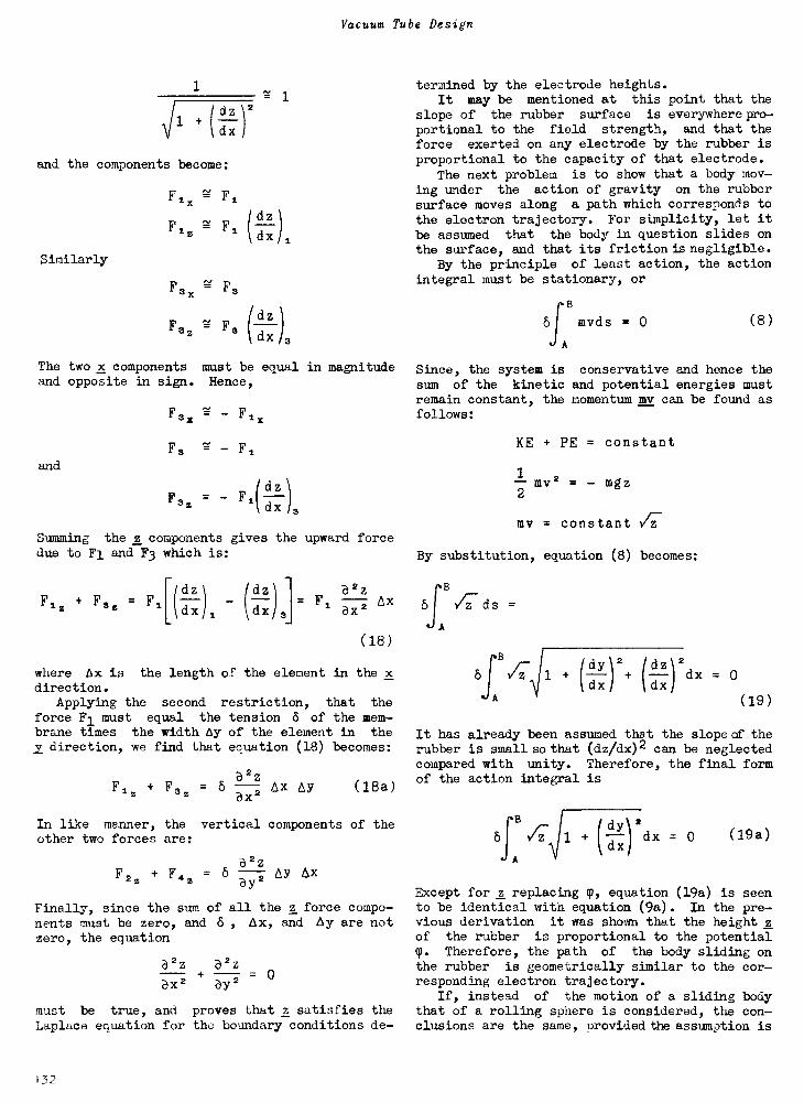
Vacuum Tube Design
1
\// d z
1 rci;
2)
and the components become:
Similarly
Fix
F13
Fax
Fez
Fi
Fi
F3
- F3
= 1
d z
dx )1
(dzdx
The two x components must be equal in magnitudeand opposite in sign. Hence,
and
F3z - Fix
F3 "---1 F1
dzF33 = Fl(t)
3
Summing the z components gives the upward forcedue to Fi and F3 which is:
F13 + F33z
= Fik7c)1 -idz
dx 31=
2z
aX2Ax
(18)
where Ax is the length of the element in the xdirection.
Applying the second restriction, that theforce F1 must equal the tension 8 of the mem-brane times the width Ay of the element in thez direction, we find that equation (18) becomes:
2z
F,3 + F33 = Ax Ay (18a)ax 2
In like manner, the vertical components of theother two forces are:
2zF23 + F43 = 8 Ay Aix
Finally, since the sum of all the z force compo-nents must be zero, and 0 , Ax, and Ay are notzero, the equation
a 2Z .B2Z- 0
ax2 aye
must be true, and proves that z satisfies theLaplace equation for the boundary conditions de-
termined by the electrode heights.It may be mentioned at this point that the
slope of the rubber surface is everywherepro-portional to the field strength, and that theforce exerted on any electrode by the rubber isproportional to the capacity of that electrode.
The next problem is to show that a body mov-ing under the action of gravity on the rubbersurface moves along a path which corresponds tothe electron trajectory. For simplicity, let itbe assumed that the body in question slides onthe surface, and that its friction is negligible.
By the principle of least action, the actionintegral must be stationary, or
B
mvds = 0
JA( 8 )
Since, the system is conservative and hence thesum of the kinetic and potential energies mustremain constant, the momentum my can be found asfollows:
KE + PE = constant
1- my 2 = - mgz2
my = constant 14-
By substitution, equation (8) becomes:
bf d S =A
idy \ 2
dx(ctzc-rdx = 0
(19)
It has already been assumed that the slope of therubber is small so that (dz/dx)2 can be neglectedcompared with unity. Therefore, the final formof the action integral is
oflizT\I 1
A
2+
dxdx = 0 (19a)
Except for z replacing 9, equation (19a) is seento be identical with equation (9a). In the pre-vious derivation it was shown that the height zof the rubber is proportional to the potentialT. Therefore, the path of the body sliding onthe rubber is geometrically similar to the cor-responding electron trajectory.
If, instead of the motion of a sliding bodythat of a rolling sphere is considered, the con-clusions are the same, orovidedthe assumption is
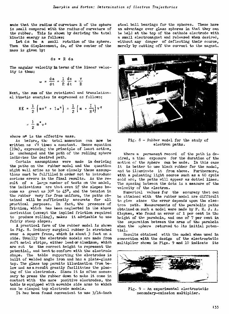
Zworykin and Norton: Determination of Electron Trajectories
made that the radius of curvature R of the sphereis small compared with the radius of curvature ofthe rubber. This is shown by deriving the totalkinetic energy as follows:
Let da be a small rotation of the sphere.Then the displacement, ds, of the center of themass is given by:
ds = R da
The angular velocity in terms of the linear veloc-ity is thus:
da 1. dsW - dt R dt
Next, the sum of the rotational and translation-al kinetic energies is expressed as follows:
1 1
2KE = -2 (my' + Iw2) = - (in + --)v2
R2
1 *= - in v22
where m* is the effective mass.As before, the total momentum can now be
written as times a constant. Hence equation(19a), expressing the principle of least action,is unchanged and the path of the rolling sphereindicates the desired path.
Certain assumptions were made in derivingthe paths on the rubber model and the questionmight well arise as to how closely these assump-tions must be fulfilled in order not to introduceserious errors in the final results. As the re-sult of a large number of tests on the model,the indications are that even if the slopes be-come as great as 300 to 450, and the tension inthe rubber very far from uniform, the paths ob-tained will be sufficiently accurate for allpractical purposes. In fact, the presence offriction, which has been neglected in the above
derivation (except the implied friction requiredto produce rolling), makes it advisable to usefairly steep slopes.
A practical form of the rubber model is shownin Fig. 8. Ordinary surgical rubber is stretchedover a square frame, which is about 3 feet on aside. Usually the electrode models are made fromsoft metal strips, either lead or aluminum, whichare cut to the correct height to represent thepotential, and bent to conform with the electrodeshape. The table supporting the electrodes isbuilt of welded angle iron and has a plate -glasstop. The glass top permits illumination from be-low and as aresult greatly facilitates the plac-ing of the electrodes. Since it is often neces-sary to press the rubber down to make it come incontact with the more positive electrodes, thetable is equipped with movable side arms to whichcan be clamped top electrode models.
It has been found convenient to use 3/16 -inch
steel ball bearings for the spheres. These havean advantage over glass spheres in that they canbe held at the top of the cathode electrode witha small electromagnet and released when desired,without any danger of deflecting their course,merely by cutting off the current to the magnet.
Fig. 8 - Rubber model for the study ofelectron paths.
Where a permanent record of the path is de-sired, a time exposure for the duration of themotion of the sphere can be made. In this caseit is better to use black rubber for the model,and to illuminate it from above. Furthermore,with a pulsating light source such as a 60 cyclecold arc, the paths will appear as dotted lines.The spacing between the dots is a measure of thevelocity of the electron.
Numerical values for the accuracy that canbe attained with the rubber model are difficultto give since the error depends upon the elec-tron path. Measurements of the parabolic pathsobtained cm. such a model were made by P. H. J. A.Kleynen, who found an error of 1 per cent in theheight of the parabola, and one of 7 per cent inthe separation between the arms of the parabolawhen the sphere returned to its initial poten-tial.
Results obtained with the model when used inconnection with the design of the electrostaticmultiplier shown in Figs. 9 and 10 indicate its
Fig. 9 - An experimental electrostaticsecondary -emission multiplier.
133
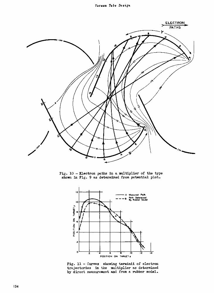
Vacuum Tube Design
Fig. 10 - Electron paths in a multiplier of the typeshown in Fig. 9 as determined from potential plot.
A Measured PathPath DeterminedBy Rubber Model
4 6 8 10 12
POSITION ON TARGET x14
Fig. 11 - Curves showing terminii of electrontrajectories in the multiplier as determinedby direct measurement and from a rubber model.
ELECTRONPATHS
134

Zworykin and Norton: Determination of Electron Trajectories
excellence. Plots were made of the initial andterminal points of a number of electrons, as in-dicated by the model, and again with an actualelectron tube. Two curves of this type are re-produced in Fig. 11, and show fairly close agree-ment between the two methods of measurement.
REFERENCES
1. J. H. Jeans, "Electricity and Magnetism,"Cambridge University Press, 1927.
2. M. Mason and W. Weaver, "The ElectromagneticField," University of Chicago Press, 1929.
3. O. D. Kellogg, "Foundations of Potential The-ory," Julius Springer, Berlin , 1929.
4. D. Gaber, "Mechanical Tracer for ElectronTrajectories," Nature, Vol. 139, p. 373; Feb-ruary 27, 1937.
5. H. Sallinger, "Tracing Electron Paths in
Electric Fields," Electronics, Vol. 10, No.10, pp. 50-54; October, 1937.
6. P. H. J. A. Kleynen, "The Motion of an Elec-tron in a Two -Dimensional ElectrostaticField," Philips Tech. Rev., Vol. 2, No.11,pp. 321-352; 1937.
7. J. R. Pierce, "Electron Multiplier Design,"Bell Tel. Record, Vol. 16, No.9, pp. 305-309; 1938.
8. V. K. Zworykinandj. A. Rajchman, "The Elec-trostatic Electron Multiplier," Proc. I.R.E.,Vol. 27, pp. 558-566; September, 1939.
135
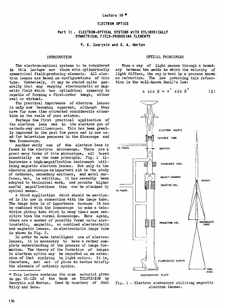
Lecture 16 *
ELECTRON OPTICS
Part II . ELECTRON -OPTICAL SYSTEMS WITH CYLINDRICALLYSYMMETRICAL FIELD -PRODUCING ELEMENTS
V. K. Zworykin and G. A. Morton
INTRODUCTION
The electron -optical systems to be consideredin this lecture are those with cylindricallysymmetrical field -producing elements. All elec-tron lenses are based on configurations of thistype. Conversely, it may be stated quite gen-erally that any varying electrostatic or mag-netic field which has cylindrical symmetry iscapable of forming a first -order image, eitherreal or virtual.
The practical importance of electron lensesis only now becoming apparent, although theyhave for some time attracted considerable atten-tion in the realm of pure science.
Perhaps the first practical application ofthe electron lens was in the electron gun ofcathode-ray oscilloscopes. This has been great-ly improved in the past few years and is now us-ed for television purposes in the Kinescope andthe Iconoscope.
Another early use of the electron lens isfound in the electron microscope. There are agreat many forms of this microscope, all basedessentially on the same principle. Fig. 1 il-lustrates a high -magnification instrument util-izing magnetic electron lenses. Not only is theelectron microscope an important aid in the studyof cathodes, secondary emitters, and metal sur-faces, but, in addition, it has recently beenadapted to biological work, and permits higheruseful magnifications than can be obtained byoptical means.
A third application which should be mention-ed is its use in connection with the image tube.The image tube is of importance because it canbe combined with the Iconoscope to make a tele-vision pickup tube which is many times more sen-sitive than the normal Iconoscope. Here again,there are a number of possible forms using elec-trostatic, magnetic, or combined electrostaticand magnetic lenses. An electrostatic image tubeis shown in Fig. 2.
In order to make intelligent use of electronlenses, it is necessary to have a rather com-plete understanding of the process of image for-mation. The theory of the formation of imagesin electron optics may be regarded as an exten-sion of that applying to light optics. It is,therefore, not out of place to review brieflythe elements of ordinary optics.
* This lecture contains the same material givenin pp. 91-120 of the book on TELEVISION by
Zworykin and Morton. Used by courtesy of John
Wiley and Sons.
OPTICAL PRINCIPLES
When a ray of light passes through a bound-ary between two media in which the velocity oflight differs, the ray is bent by a process knownas refraction. The law governing this refrac-tion is the well-known Snell's law:
n sin R = nt sin
TO PUMPS
TO PUMPS
to
ELECTRON SOURCE
FLEXIBLE TUBE
SHUTTER
CONDENSER COIL
OBJECT CHAMBER
OBJECTIVE COIL
PROJECTION COIL
FLUORESCENT SCREEN
PHOTOGRAPHIC PLATE
(1)
OBJECT
INTERMEDIATEIMAGE
4' FINALIMAGE
Fig. 1 - Electron microscope utilizing magneticelectron lenses.
136
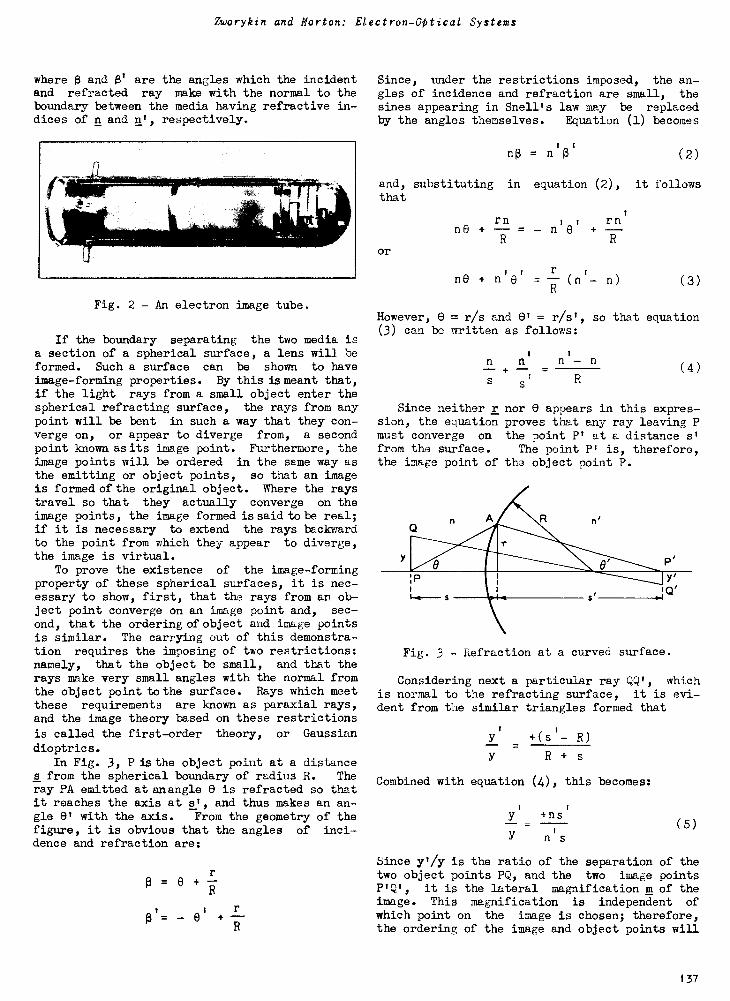
Zworykin and Norton: Electron -Optical Systems
where 6 and 6' are the angles which the incidentand refracted ray make with the normal to theboundary between the media having refractive in-dices of n and n', respectively.
Fig. 2 - An electron image tube.
If the boundary separating the two media isa section of a spherical surface, a lens will beformed. Such a surface can be shown to haveimage -forming properties. By this is meant that,if the light rays from a small object enter thespherical refracting surface, the rays from anypoint will be bent in such a way that they con-verge on, or appear to diverge from, a secondpoint known as its image point. Furthermore, theimage points will be ordered in the same way asthe emitting or object points, so that an imageis formed of the original object. Where the raystravel so that they actually converge on theimage points, the image formed is said to be real;if it is necessary to extend the rays backwardto the point from which they appear to diverge,the image is virtual.
To prove the existence of the image -formingproperty of these spherical surfaces, it is nec-essary to show, first, that the rays from an ob-ject point converge on an image point and, sec-
ond, that the ordering of object and image pointsis similar. The carrying out of this demonstra-tion requires the imposing of two restrictions:namely, that the object be small, and that therays make very small angles with the normal fromthe object point to the surface. Rays which meetthese requirements are known as paraxial rays,and the image theory based on these restrictions
is called the first -order theory, or Gaussian
dioptrics.In Fig. 3, P is the object point at a distance
s from the spherical boundary of radius R. Theray PA emitted at mangle 6 is refracted so thatit reaches the axis at s', and thus mikes an an-gle 8' with the axis. From the geometry of thefigure, it is obvious that the angles of inci-dence and refraction are:
0 = e
e. r
Since, under the restrictions imposed, the an-gles of incidence and refraction are small, thesines appearing in Snell's law may be replacedby the angles themselves. Equation (1) becomes
n6 = n 6t (2)
and, substituting in equation (2), it followsthat
or
ne +rn
= - +rn
R
ne + n1 et (nt- n) (3)
However, 8 = r/s and 6' = r/s', so that equation(3) can be written as follows:
n n nt- n+
R(4)
Since neither r nor 8 appears in this expres-sion, the equation proves that any ray leaving Pmust converge on the point P' at a distance s'from the surface. The point P' is, therefore,the image point of the object point P.
Fig. 3 - Refraction at a curved surface.
Considering next a particular ray QQ', whichis normal to the refracting surface, it is evi-dent from the similar triangles formed that
y
y
+(s' - R)
R + s
Combined with equation (4), this becomes:
+ns'(5)
n- os
Since y'/y is the ratio of the separation of thetwo object points PQ, and the two image pointsP'Q', it is the lateral magnification m of theimage. This magnification is independent ofwhich point on the image is chosen; therefore,the ordering of the image and object points will
137
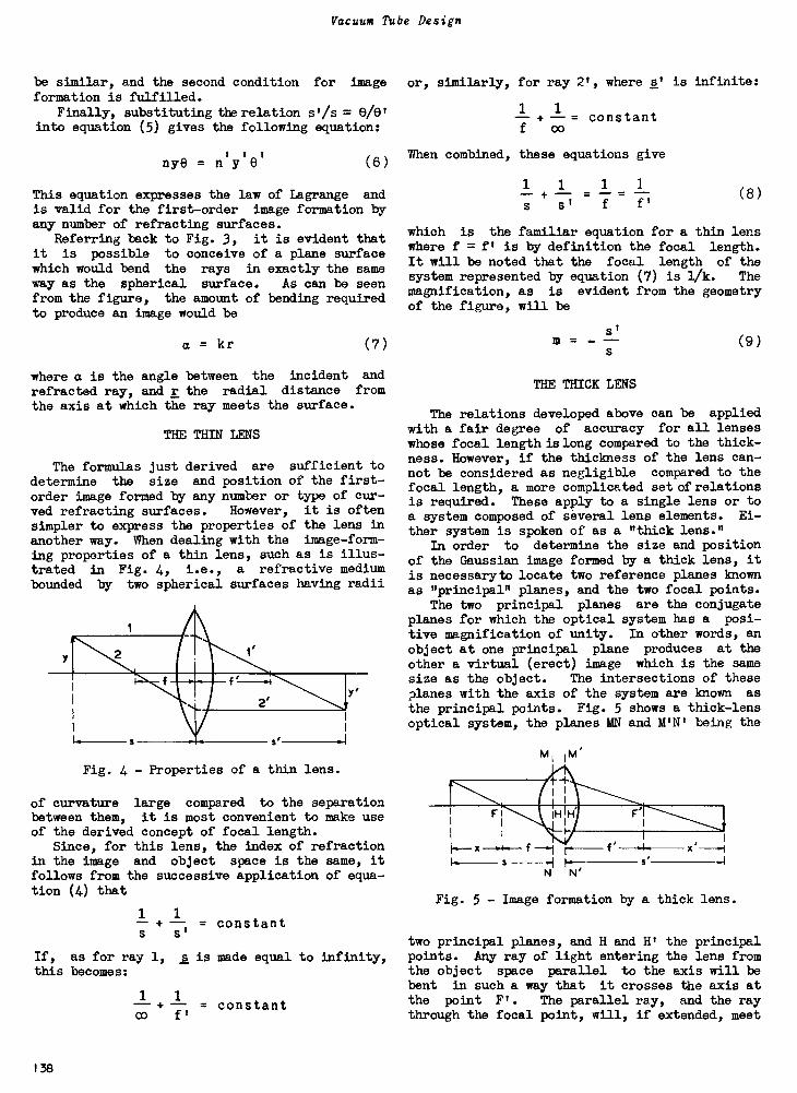
Vacuum Tube Design
be similar, and the second condition for imageformation is fulfilled.
Finally, substituting the relation s'/s=into equation (5) gives the following equation:
nye=nIyIeI (6)
This equation expresses the law of Lagrange andis valid for the first -order image formation byany number of refracting surfaces.
Referring back to Fig. 3, it is evident thatit is possible to conceive of a plane surfacewhich would bend the rays in exactly the sameway as the spherical surface. As can be seenfrom the figure, the amount of bending requiredto produce an image would be
a = kr (7)
where a is the angle between the incident andrefracted ray, and r the radial distance fromthe axis at which the ray meets the surface.
THE THIN LENS
The formulas just derived are sufficient to
determine the size and position of the first -
order image formed by any number or type of cur-ved refracting surfaces. However, it is oftensimpler to express the properties of the lens inanother way. When dealing with the image -form-
ing properties of a thin lens, such as is illus-trated in Fig. 4, i.e., a refractive mediumbounded by two spherical surfaces having radii
Fig. 4 - Properties of a thin lens.
of curvature large compared to the separationbetween them, it is most convenient to make useof the derived concept of focal length.
Since, for this lens, the index of refractionin the image and object space is the same, itfollows from the successive application of equa-tion (4) that
1+
1- = constants'
If, as for ray 1, s is made equal to infinity,this becomes:
1- + 1- = constantoo f
or, similarly, for ray 2', where s' is infinite:
1 1- + -= constantf oo
When combined, these equations give
1 1 1 1- = - -s' f f
( 8 )
which is the familiar equation for a thin lenswhere f = fl is by definition the focal length.It will be noted that the focal length of thesystem represented by equation (7) is 1/k. Themagnification, as is evident from the geometryof the figure, will be
m = --s
THE THICK LENS
(9)
The relations developed above can be appliedwith a fair degree of accuracy for all lenseswhose focal length is long compared to the thick-ness. However, if the thickness of the lens can-not be considered as negligible compared to thefocal length, a more complicated set of relationsis required. These apply to a single lens or toa system composed of several lens elements. Ei-ther system is spoken of as a "thick lens."
In order to determine the size and positionof the Gaussian image formed by a thick lens, itis necessary to locate two reference planes knownas "principal" planes, and the two focal points.
The two principal planes are the conjugateplanes for which the optical system has a posi-tive magnification of unity. In other words, anobject at one principal plane produces at theother a virtual (erect) image which is the samesize as the object. The intersections of theseplanes with the axis of the system are known as
the principal points. Fig. 5 shows a thick -lensoptical system, the planes MN and M'N' being the
FI
M M'
x
N N'
Fig. 5 - Image formation by a thick lens.
two principal planes, and H and H' the principalpoints. Any ray of light entering the lens fromthe object space parallel to the axis will bebent in such a way that it crosses the axis atthe point F'. The parallel ray, and the raythrough the focal point, will, if extended, meet
138
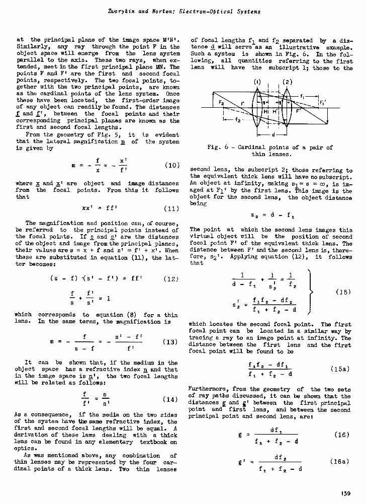
Zworykin and Norton: Electron -Optical Systems
at the principal plane of the image space M'N'.Similarly, any ray through the point F in theobject space will emerge from the lens systemparallel to the axis. These two rays, when ex-tended, meet Lithe first principal plane MN. Thepoints F and F' are the first and second focalpoints, respectively. The two focal points, to-gether with the two principal points, are knownas the cardinal points of the lens system. Oncethese have been located, the first -order imageof any object can readily be found. The distancesf and f', between the focal points and theircorresponding principal planes are known as thefirst and second focal lengths.
From the geometry of Fig. 5, it is evidentthat the lateral magnification m of the systemis given by
f x'm = _ =--
x f'(10)
where x and x' are object and image distancesfrom the focal points. From this it followsthat
xx' = ff' (11)
The magnification and position can, of course,be referred to the principal points instead ofthe focal points. If s and s' are the distancesof the object and image from the principal planes,their valuesares = x + f and st = ft + x'. Whenthese are substituted in equation (11), the lat-ter becomes:
of focal lengths fl and f2 separated by a dis-tance d will serve as an illustrative example.Such a system is shown in Fig. 6. In the fol-lowing, all quantities referring to the firstlens will have the subscript 1; those to the
Fig. 6 - Cardinal points of a pair ofthin lenses.
second lens, the subscript 2; those referring tothe equivalent thick lens will have no subscript.An object at infinity, making si= s = op, is im-aged at F1' by the first lens. This image is theobject for the second lens, the object distancebeing
s, = d - fi
The point at which the second lens images thisvirtual object will be the position of secondfocal point F' of the equivalent thick lens. Thedistance between F' and the second lens is, there-fore, s2,. Applying equation (12), it followsthat
which
(s - - f') = (12)
f f'= 1
s'
corresponds to equation (8) for a thin
1 1 1-(15)
+d - f, s2 f2
fife - df2-
f1 f2 - dlens. In the same terms, the magnification is which locates the second focal point. The first
m -f s' f'
(13)s - f f'
It can be shown that, if the medium in theobject space has a refractive index n and thatin the image space is nt, the two focal lengthswill be related as follows:
f' n'(14)
As a consequence, if the media on the two sidesof the system have the same refractive index, thefirst and second focal lengths will be equal. Aderivation of these laws dealing with a thicklens can be found in any elementary textbook onoptics.
As was mentioned above, any combination ofthin lenses may be represented by the four car-dinal points of a thick lens. Two thin lenses
focal point can be located in a similar way bytracing a ray to an image point at infinity. Thedistance between the first lens and the firstfocal point will be found to be
fife - df,f, + f2 - d (15a)
Furthermore, from the geometry of the two setsof ray paths discussed, it can be shown that thedistances g and gt between the first principalpoint and first lens, and between the secondprincipal point and second lens, are:
df,g - f, + f, - d
g df 2
f, + f, - d
139
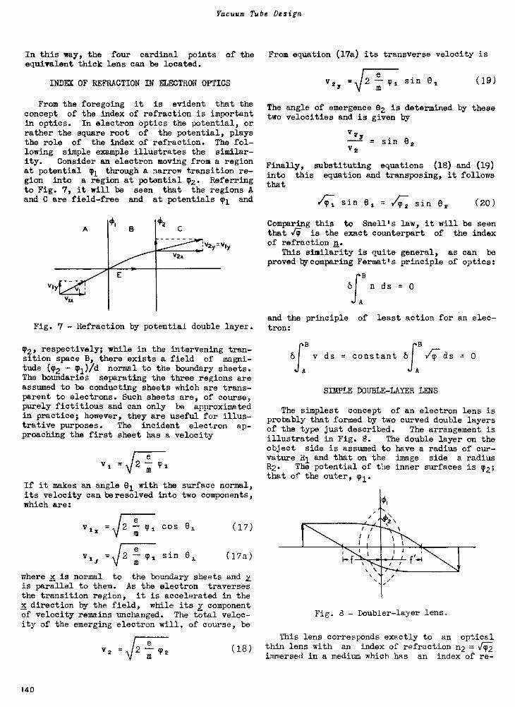
Vacuum Tube Design
In this way, the four cardinal points of theequivalent thick lens can be located.
INDEX OF REFRACTION IN ELECTRON OPTICS
From the foregoing it is evident that theconcept of the index of refraction is importantin optics. In electron optics the potential, orrather the square root of the potential, playsthe role of the index of refraction. The fol-lowing simple example illustrates the similar-ity. Consider an electron moving from a regionat potential Ti through a narrow transition re-gion into a region at potential T2. Referringto Fig. 7, it will be seen that the regions Aand C are field -free and at potentials yi and
Fig. 7 - Refraction by potential double layer.
X12, respectively; while in the intervening tran-sition space B, there exists a field of magni-tude (T2 - T1)/d normal to the boundary sheets.The boundaries separating the three regions areassumed to be conducting sheets which are trans-parent to electrons. Such sheets are, of course,purely fictitious and can only be approximatedin practice; however, they are useful for illus-trative purposes. The incident electron ap-proaching the first sheet has a velocity
ev1 = .2 --m y
If it makes an angle 01 with the surface normal,its velocity can be resolved into two components,which are:
Ni
evix=2---(pi cos e1
m(17)
1=,12 -cps sin 81 (17a)
where x is normal to the boundary sheets and yis parallel to them. As the electron traversesthe transition region, it is accelerated in thex direction by the field, while its y componentof velocity remains unchanged. The total veloc-ity of the emerging electron will, of course, be
V2 = .2ID
(P2
From equation (17a) its transverse velocity is
v27 =,j223` .\/2 -e cp, sin 81 (19)
The angle of emergence 02 is determined by thesetwo velocities and is given by
V2y
V2= sin 82
Finally, substituting equations (18) and (19)into this equation and transposing, it followsthat
'4171 sin 81 = AZ sin 82 (20)
Comparing this to Snell's law, it will be seenthat v is the exact counterpart of the indexof refraction n.
This similarity is quite general, as can beproved by comparing Fermat's principle of optics:
bf n ds = 0
A
and the principle of least action for an elec-tron:
ofBA v ds = constant 6 14-ds = 0
A
SIMPLE DOUBLE -LAYER LENS
The simplest concept of an electron lens isprobably that formed by two curved double layersof the type just described. The arrangement isillustrated in Fig. 8. The double layer on theobject side is assumed to have a radius of cur-vature R1 and that on the image side a radiusR2. The potential of the inner surfaces is y2;that of the outer, 'Pi.
Fig. 8 - Doubler -layer lens.
This lens corresponds exactly to an optical
(18) thin lens with an index of refraction n2 =immersed in a medium which has an index of re -
140
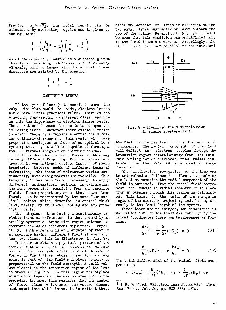
Zworykin and Morton: Electron -Optical Systems
fraction Its focal length can be
calculated by elementary optics and is given bythe equation:
1f
=1 1
- 1) ( )II, 1,2
An electron source, located at a distance s fromthis lens, emitting electrons with a velocity12(e/m)91 will be imaged at a distance s'. Thesedistances are related by the equation
1 1 1
s' f
CONTINUOUS LENSES
If the type of lens just described were the
only kind that could be made, electron lenseswould have little practical value. There existsa second, fundamentally different class, and up-on this the importance of electron lenses rests.The operation of these lenses is based upon thefollowing fact: Whenever there exists a regionin which there is a varying electric field hav-ing cylindrical symmetry, this region will haveproperties analogous to those of an optical lenssystem; that is, it will be capable of forming areal or virtual image of an emitting source.
It is evident that a lens formed in this wayis very different from the familiar glass lenstreated in conventional optics. Instead of sharpboundaries between media of different index ofrefraction, the index of refraction varies con-tinuously, both along the axis and radially. Thisbeing so, it has been found necessary to applydifferent mathematical methods in calculatingthe lens properties resulting from any specificfield. These properties, once they have beenfound, can be represented by the same four car-dinal points which describe an optical thicklens, namely, by two focal points and two prin-cipal points.
The simplest lens having a continuously va-riable index of refraction is that formed by anaxially symmetric transition region between twoconstant fields of different magnitude. Physi-cally, such a region is approximated by that inan aperture having different field strengths onthe two sides. This is illustrated in Fig. 9a.
In order to obtain a physical picture of theaction of this lens, it is convenient to makeuse of the concept of lines of electrostaticforce, or field lines, whose direction at anypoint is that of the field and whose density isproportional to the field strength. A small vol-ume element in the transition region of the lensis shown in Fig. 9b. In this region the Laplaceequation is obeyed and, as was pointed out in thepreceding lecture, this requires that the numberof field lines which enter the volume elementmust equal that which leave. It is evident that,
since the density of lines is different on thetwo ends, lines must enter or leave through thetop of the volume. Referring to Fig. 9b, it willbe seen that this condition can be fulfilled onlyif the field lines are curved. Accordingly, thefield lines are not parallel to the axis, and
(a)
(b)
Ei E2
ErE,
1....____a
-ad
Fig. 9 - Idealized field distributionin simple aperture lens.
the field can be resolved into radial and axialcomponents. The radial component of the fieldwill deflect any electron passing through thetransition region toward (or away from) the axis.This bending action increases with radial dis-tance from the axis, as is required for imageformation.
The quantitative properties of the lens canbe determined as follows:1 First, by applyingthe Laplace equation the radial component of thefield is obtained. From the radial field compo-nent the change in radial momentum of an elec-tron in passing through this region is calculat-ed. This leads to the value of the change inangle of the electron trajectory and, hence, di-rectly to the focal length of the system.
Since there are no charges, the divergence aswell as the curl of the field are zero. In cylin-drical coordinates these can be expressed as fol-lows:
and
3Ez+ - -(rEr) = 0 (21)
az r ar
a
az---(rEr ) - r
ar= 0 (22)
1 a
aEz
The total differential of the radial field com-ponent is
d (rEr) =az
(rEra
) dz +a-r(rEr ) dr
1 L.H. Bedford, "Electron Lens Formulas," Phys.
Soc. Proc., Vol. 46, pp. 882-888; 1934.
141
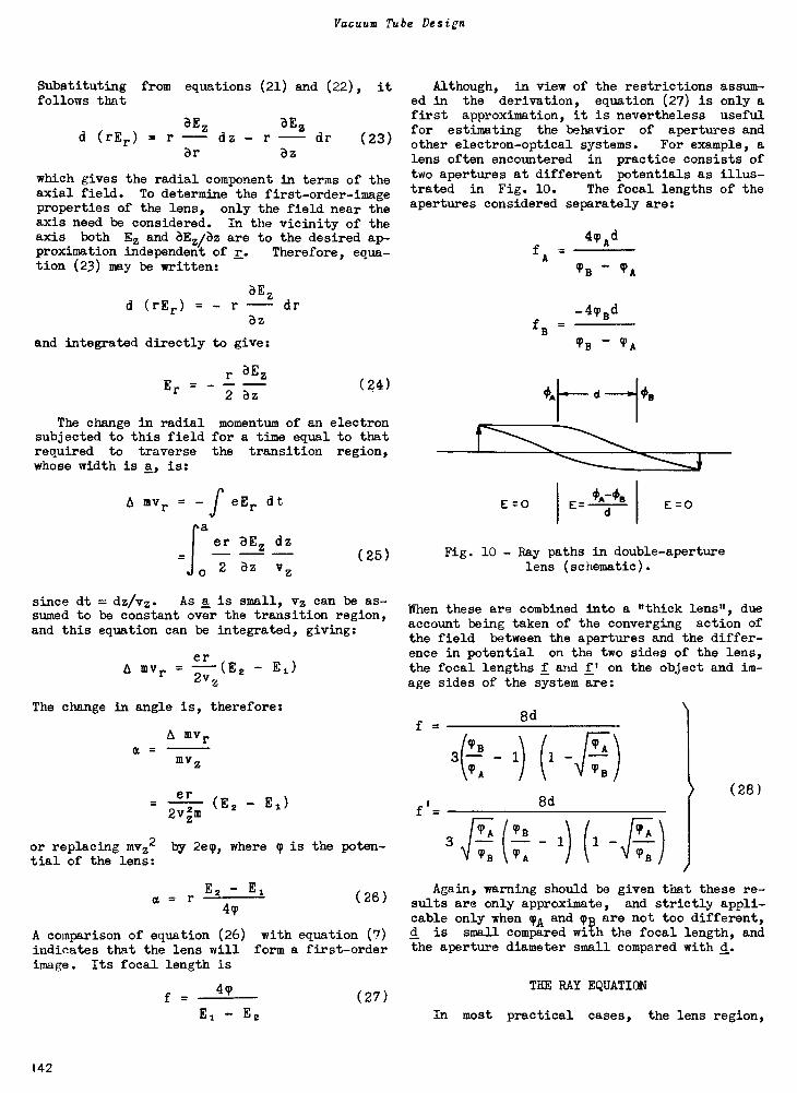
Vacuum Tube Design
aEzd (rEr) = r dz - r dr (23)ar az
which gives the radial component in terms of theaxial field. To determine the first -order -imageproperties of the lens, only the field near theaxis need be considered. In the vicinity of theaxis both Ez and aEz/az are to the desired ap-proximation independent of r. Therefore, equa-tion (23) may be written:
d (rEr) = - raEz
draz
and integrated directly to give:
r aEzEr ' 2 az (24)
The change in radial momentum of an electronsubjected to this field for a time equal to thatrequired to traverse the transition region,whose width is a, is:
A mvr = -f eEr dta
er aEz dz
0 2 az vz
Although, in view of the restrictions assum-ed in the derivation, equation (27) is only afirst approximation, it is nevertheless usefulfor estimating the behavior of apertures andother electron -optical systems. For example, alens often encountered in practice consists oftwo apertures at different potentials as illus-trated in Fig. 10. The focal lengths of theapertures considered separately are:
fA
-
fB
-
41pAd
PB 'A
-LipBd
CPB - CPA
cat- d ca.
E=0 E= °A45 E =0
(25) Fig. 10 - Ray paths in double -aperturelens (schematic).
since dt = dz/vz. As a is small, vz can be as-sumed to be constant over the transition region,and this equation can be integrated, giving:
erA mvr =
2v(E2 - E1)
z
The change in angle is, therefore:
a -
Substituting from equations (21) and (22), itfollows that
aEz
A mvr
MVz
er (E2 - E1)2v:m
or replacing mvz2 by 2e9, where p is the poten-tial of the lens:
E2 - El
4'
A comparison of equation (26)indicates that the lens willimage. Its focal length is
= r (26)
with equation (7)form a first -order
f =4p
Ei - E2(27)
When these are combined into a "thick lens", dueaccount being taken of the converging action ofthe field between the apertures and the differ-ence in potential on the two sides of the lens,the focal lengths f and ft on the object and im-age sides of the system are:
f -
(28)f
Again, warning should be given that these re-sults are only approximate, and strictly appli-cable only when PA and 913 are not too different,d is small compared with the focal length, andthe aperture diameter small compared with d.
THE RAY EQUATION
In most practical cases, the lens region,
142
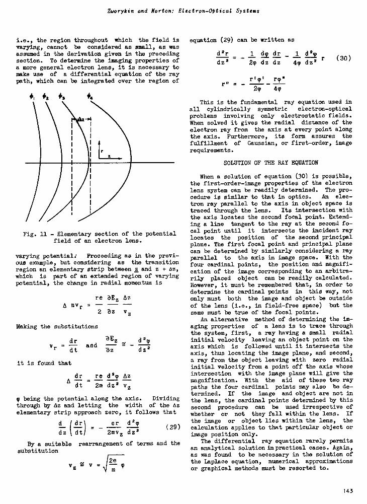
Zworykin and Norton: Electron -Optical Systems
i.e., the region throughout which the field isvarying, cannot be considered as small, as wasassumed in the derivation given in the precedingsection. To determine the imaging properties ofa more general electron lens, it is necessary tomake use of a differential equation of the raypath, which can be integrated over the region of
#1 42 +3 44
Fig. 11 - Elementary section of the potentialfield of an electron lens.
varying potential: Proceeding as in the previ-ous example, but considering as the transitionregion an elementary strip between z and z + Az,which is part of an extended region of varyingpotential, the change in radial momentum is
re Hz Azmyr = - - -
2 Bz vz
Making the substitutions
ZEzdr-v= anddt -az
it is found that
dr re d2m AzA = -
dt 2m dz2 vz
d 2p
dz2
9 being the potential along the axis. Dividingthrough by Az and letting the width of the Azelementary strip approach zero, it follows that
d
(dt= er d29
dz dti 2mvz dz2
By a suitable rearrangement of terms and thesubstitution
2evz = v m
m
(29)
equation (29) can be written as
der 1 Al dr 1 d2p
dz2 2, dz dz 4T dz2 r (30)
r"r'q
2p 4p
This is the fundamental ray equation used inall cylindrically symmetric electron -optical
problems involving only electrostatic fields.When solved it gives the radial distance of the
electron ray from the axis at every point alongthe axis. Furthermore, its form assures the
fulfillment of Gaussian, or first -order, image
requirements.
SOLUTION OF THE RAY EQUATION
When a solution of equation (30) is possible,the first -order -image properties of the electronlens system can be readily determined. The pro-cedure is similar to that in optics. An elec-tron ray parallel to the axis in object space istraced through the lens. Its intersection withthe axis locates the second focal point. Extend-ing a line tangent to the ray at the second fo-cal point until it intersects the incident raylocates the position of the second principalplane. The first focal point and principal planecan be determined by similarly considering a rayparallel to the axis in image space. With thefour cardinal points, the position and magnifi-cation of the image corresponding to an arbitra-rily placed object can be readily calculated.However, it must be remembered that, in order todetermine the cardinal points in this way, not
only must both the image and object be outsideof the lens (i.e., in field -free space) but thesame must be true of the focal points.
An alternative method of determining the im-aging properties of a lens is to trace throughthe system, first, a ray having a small radialinitial velocity leaving an object point on theaxis which is followed until it intersects theaxis, thus locating the image plane, and second,a ray from the object leaving with zero radialinitial velocity from a point off the axis whoseintersection with the image plane will give themagnification. With the aid of these two raypaths the four cardinal points may also be de-termined. If the image and object are not inthe lens, the cardinal points determined by thissecond procedure can be used irrespective ofwhether or not they fall within the lens. If
the image or object lies within the lens, the
calculation applies to that particular object orimage position only.
The differential ray equation rarely permitsan analytical solution in practical cases. Again,as was found to be necessary in the solution ofthe Laplace equation, numerical approximationsor graphical methods must be resorted to.
143
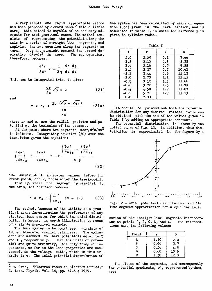
Vacuum Tube Design
A very simple and rapid approximate methodhas been proposed by Richard Gans.2 With a littlecare, this method is capable of an accuracy ad-equate for most practical cases. The method con-sists of representing the potential along theaxis by a series of straight-line segments, andapplying the ray equation along the segments inturn. Over any straight segment the second de-rivative d2p/dz2 is zero. The ray equation,therefore, becomes:
der 1 dr dy
dz2 = -2y dz dz
This can be integrated twice to give:
and
r = ro
1E Cdz
2C (/- )
dz
(31)
(31a)
where ro and To are the radial position and po-tential at the beginning of the segment.
At the point where two segments meet,d2p/dz2is infinite. Integrating equation (30) over thetransition gives the equation:
(4) taT\tdr l (dr\ kaz)2 azi,
\dz/2 kdzi, 4 y
(32)
The subscript 1 indicates values before thebreak-point, and 2, those after the break-point.
Finally, where the segment is parallel tothe axis, the solution becomes
drr = ro + (-)zo
dz(33)
The method, because of its utility as a prac-tical means for estimating the performance of anyelectron lens system for which the axial distri-bution is known, is worth illustrating by meansof a simple numerical example.
The lens system to be considered consists oftwo equidiameter coaxial cylinders. The cylin-ders are assumed to have potentials equal to 2and 12, respectively. Here the units of poten-tial are quite arbitrary, the only thing of im-portance, as far as the lens properties are con-cerned, is the voltage ratio, which in this ex-ample is 6. The axial potential distribution of
2 R. Gans, "Electron Paths in Electron Optics,"Z. tech. Physik, Vol. 18, pp. 41-48; 1937.
the system has been calculated by means of equa-tion (35a) given in the next section, and istabulated in Table I, in which the distance z isgiven in cylinder radii.
Table I
z 9 z 9
-2.0 2.05 0.1 7.66-1.8 2.10 0.3 8.88-1.6 2.16 0.5 9.88-1.4 2.27 0.7 10.62-1.2 2.44 0.9 11.12-1.0 2.70 1.1 11.45-0.8 3.12 1.3 11.66-0.6 3.72 1.5 11.79
-0.4 4.58 1.7 11.87-0.2 5.71 1.9 11.930.0 7.00
It should be pointed out that the potentialdistribution for any desired voltage ratio canbe obtained with the aid of the values given inTable I by adding an appropriate constant.
The potential distribution is shown by thedotted curve of Fig. 12. In addition, this dis-tribution is approximated in the figure by a
Fig. 12 - Axial potential distribution and itsline segment approximation for a cylinder lens.
series of six straight-line segments intersect-ing at points A, B, C, D, and E. The intersec-tions have the following values:
Point z T
A -1.60 2.0B -0.96 2.7C -0.46 4.3D 0.60 10.6E 1.40 12.0
The slopes of the segments, and consequentlythe potential gradients, p', represented by them,are:
144
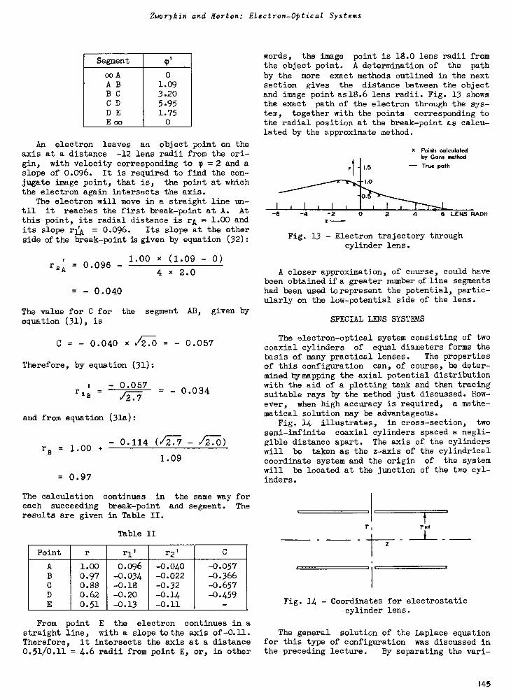
Zworykin and Morton: Electron -Optical Systems
Segment 9'
aDA 0
A B 1.09B C 3.20C D 5.95D E 1.75Eoo 0
An electron leaves an object point on theaxis at a distance -12 lens radii from the ori-gin, with velocity corresponding to 9 =2 and aslope of 0.096. It is required to find the con-jugate image point, that is, the point at whichthe electron again intersects the axis.
The electron will move in a straight line un-til it reaches the first break-point at A. Atthis point, its radial distance is rA = 1.00 andits slope rA = 0.096. Its slope at the otherside of the break-point is given by equation (32):
r2A = 0.0961.00 x (1.09 - 0)
4 x 2.0
= - 0.040
The value for C for the segment AB, given by
equation (31), is
C = - 0.040 x /TO = - 0.057
Therefore, by equation (31):
- 0.057r = - - 0.034
and from equation (31a):
- 0.114 (/277 - /F i5)rB = 1.00 +1.09
= 0.97
The calculation continues in the same way foreach succeeding break-point and segment. Theresults are given in Table II.
Table II
Point r r11 r2' C
A 1.00 0.096 -0.040 -0.057B 0.97 -0.034 -0.022 -0.366C 0.88 -0.18 -0.32 -0.657D 0.62 -0.20 -0.14 -0.459E 0.51 -0.13 -0.11 -
From point E the electron continues in astraight line, with a slope to the axis of -0.11.Therefore, it intersects the axis at a distance0.51/0.11 = 4.6 radii from point E, or, in other
words, the image point is 18.0 lens radii fromthe object point. A determination of the path
by the more exact methods outlined in the nextsection gives the distance between the objectand image point as 18.6 lens radii. Fig. 13 showsthe exact path of the electron through the sys-tem, together with the points corresponding tothe radial position at the break-point as calcu-lated by the approximate method.
x Points calculatedby Gans method
1.5 - True path
1.0
-2 4 6 LENS RADII
Fig. 13 - Electron trajectory throughcylinder lens.
A closer approximation, of course, could havebeen obtained if a greater number of line segmentshad been used to represent the potential, partic-ularly on the low -potential side of the lens.
SPECIAL LENS SYSTEMS
The electron -optical system consisting of twocoaxial cylinders of equal diameters forms thebasis of many practical lenses. The propertiesof this configuration can, of course, be deter-mined by mapping the axial potential distributionwith the aid of a plotting tank and then tracingsuitable rays by the method just discussed. How-ever, when high accuracy is required, a mathe-matical solution may be advantageous.
Fig. 14 illustrates, in cross-section, two
semi -infinite coaxial cylinders spaced a negli-gible distance apart. The axis of the cylinderswill be taken as the z-axis of the cylindricalcoordinate system and the origin of the systemwill be located at the junction of the two cyl-inders.
r
z
Fig. 14 - Coordinates for electrostaticcylinder lens.
The general solution of the Laplace equationfor this type of configuration was discussed inthe preceding lecture. By separating the vari-
145
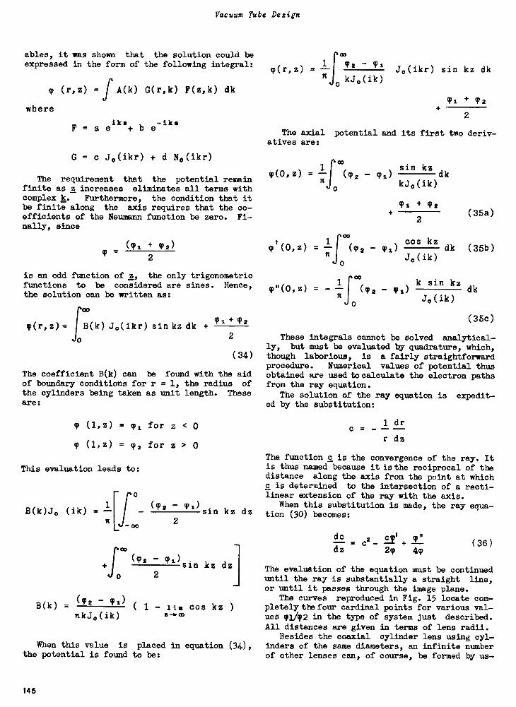
Vacuum Tube Design
ables, it was shown that the solution could beexpressed in the form of the following integral:
p (r,z) =fA(k) G(r,k) F(z,k) dk
where
F = a eiks b e-iks
G = c J0(ikr) + d N0(ikr)
The requirement that the potential remainfinite as z increases eliminates all terms withcomplex k. Furthermore, the condition that itbe finite along the axis requires that the co-efficients of the Neumann function be zero. Fi-nally, since
-((Pt T2)
2
is an odd function of z, the only trigonometricfunctions to be considered are sines. Hence,the solution can be written as:
141)(r, z) = B(k) Jo(ikr) sin kz dk + i + CP2
00
2
(34)
The coefficient B(k) can be found with the aidof boundary conditions for r = 1, the radius ofthe cylinders being taken as unit length. Theseare:
T (1,z) = yl for z < 0
T (1,z) = T2 for z > 0
This evaluation leads to:
=-
B(k)J, (ik)f (P2 fl)sin kz dz
-00 2
if: (TS
B(k) =2 Ts)
nkJo(ik)
- Ti)sin kz dz2
( 1 - iss cos kz16-10.02
When this value is placed in equation (34),the potential is found to be:
rjp(r,z) = 1 P2 - C71 Jo(ikr) sin kz dk
0kJ, (ik)
Ts + T2
2
The axial potential and its first two deriv-atives are:
,(0,Z) = (P20
00
T'(0,z) = fo
sin kzdk
kJ,(ik)
Ta (1/2
2(35a)
cos kz- Ts) dk (35b)
J0(ik)
001
T"(°'2) = (Ta - Ts)k sin kz
0Jo(ik)
dk
(35c)
These integrals cannot be solved analytical-ly, but must be evaluated by quadrature, which,though laborious, is a fairly straightforwardprocedure. Numerical values of potential thusobtained are used to calculate the electron pathsfrom the ray equation.
The solution of the ray equation is expedit-ed by the substitution:
1 drC =
r dz
The function c is the convergence of the ray. Itis thus named because it is the reciprocal of thedistance along the axis from the point at whichc is determined to the intersection of a recti-linear extension of the ray with the axis.
When this substitution is made, the ray equa-tion (30) becomes:
dc 2 Cf1 T"= c - +dz 2p 4T
(36)
The evaluation of the equation must be continueduntil the ray is substantially a straight line,or until it passes through the image plane.
The curves reproduced in Fig. 15 locate com-pletely the four cardinal points for various val-ues '142 in the type of system just described.All distances are given in terms of lens radii.
Besides the coaxial cylinder lens using cyl-inders of the same diameters, an infinite numberof other lenses can, of course, be formed by us -
146
Zworykin and Norton: Electron -Optical Systems
ing cylinders of unequal diameters. The effectof this difference is to alter to some extentthe position of the cardinal points. From the
standpoint of Gaussian dioptrics, there is rare-ly any advantage in choosing cylinders of dif-ferent diameters. Empirical data, however, in-dicate that certain of the image defects can beconsiderably reduced by a proper selection ofdiameter ratios.
4
-8
r. F
+I I 02
r ; 1-e- r2fy ---
,
H2
ow
.0
do*go.
00. on*
firT42
Fig. 15 - Focal length and position of focalpoints of cylinder as function of voltage ratio
(after Epstein, reference 16).
APERTURE LENSES
Another very important class of lenses arethose formed by a pair of apertured conductorsat different potentials. Lenses of this classare used extensively both in the electron gunand in electron imaging devices such as the mi-croscope.
The simplest lens of this type has alreadybeen discussed. The results obtained for thisrestricted case, however, have very limited ap-plication. They can be used only where the po-tential difference of the apertures is small sothat the focal lengths are large compared to thespacing between the apertures and to their diam-eters.
A determination of the first -order -image prop-erties of aperature lenses has been made by Polo-tovski by electrolytic and graphical methods.Fig. 16 reproduces some of his results. These
curves give the second focal length for variousvoltages, and separation -to -diameter ratios. Forcomparison, equation (28) for the simplified caseis included in this figure.
CATHODE LENS SYSTEMS
In many practical electron -optical lenses,the electrons enter the system with essentiallyzero velocity. Such a lens is to be found in theelectrostatically focused image tube. This typeof lens, shown in Fig. 17, differs quite radical-ly in its properties from the lenses discussedso far.
20
f24,
10
IIIII
f, =f2N2f1 . First
11116,
,47, Length
IILL'' ..._.. ,wmw._
ERB
0
02/4,,
10 15
0 4
=.82
=1.24=1.73=3.75
Fig. 16 - Focal length of double -aperture lenses(after Polotovski, reference 15).
The potential at the point where the electronenters the system is zero. In consequence, theelectron ray originates in a region of zero indexof refraction. Because of this condition, thefirst focal length is zero and the first princi-pal plane is located at the object.
LENS
OBJECT IMAGE
CATHODE CYLINDER ANODE CYLINDER
Fig. 17 - Cathode lens.
Under these conditions, if the electrons wereactually emitted from the object, that is, thecathode, with zero velocity, the image plane
147
Vacuum Tube Design
would be completely indeterminate. However, theassumption of a small radial initial velocitysuffices to determine the position and, with it,the magnification of the image. In practice,both the radial and axial components of the in-itial velocity are far from negligible, and areresponsible for certain aberrations to be dis-cussed in the following lecture.
One of the simplest lenses of this type con-sists of two coaxial cylinders of equal diam-eter, one infinite in extent, the other termi-nated by a flat plane. The terminal plane is
assumed to be the electron object. In a conven-tional image tube, for example, this plane wouldbe a photoelectric cathode. The cathode surfaceis conducting and is electrically connected tothe cathode cylinder, these elements being atzero potential. For convenience, the lens willbe said to be located at the junction of the twocylinders, although actually it extends from thecathode to a distance of several cylinder radiibeyond the junction. The geometry of the lenscan be seen from Fig. 17.
The calculation of the potential distributionproceeds exactly as in the previous example ofthe two -cylinder lens. It is expedient here touse cylindrical coordinates with their origin atthe cathode. The general solution of the Laplaceequation, which can be evaluated from the bound-ary conditions of the lens, leads to the follow-ing integrals which give the potential along theaxis together with the first and second derive-,tives:
y(0, =2
feo°
cos kunPtJo
00
y (0,2
= ni (pi
0
k
sin kz
(1k)
cos ku cos kz
dk (37a)
Jo (ik)dk (37b)
00
n2 k cos ku sin kz
cp(0,z)= --I Ti dkn
0 Jo (ik)
(37c)
As before, these integrals must be evaluated byquadrature.
The numerical values of the potential thusobtained can, with the aid of the ray equation,be used to obtain the lens properties. In thisinstance, the convergence function, c, becomesinfinite at z = 0 and thus cannot be used. How-ever, substitution of the function:
1 1 dr
2 z r dz
leads to:
db 2- = b - b
(.1. cp" 1 ( yr 1
z +2p) 4y 2 z 2 cp 2z)
and thus facilitates the solution by reducingthe ray equation to a first -order differentialequation.
Numerical determinations of two electron pathswill locate the image and give its magnification.In Fig. 18 the potential and its first two deriv-atives are shown, together with two electron
1.0
Op"
/ \0.5 /
/// //
1.0 2.0
-0.5 \ /
4.0 z(LENS RADII)
u =1.8 LENS RADII
1.0 2.0
Fig. 18 - Axial potential distribution and elec-tron trajectories in a cathode lens.
trajectories. It should be noted that the latterare independent of the applied potential, P1, andare a function of the cathode -to -lens distance,u, only. The relations between image distance,object distance, and magnification are given inFig. 19a.
It is often desirable to arrange the lens insuch a way that the focal length and image posi-tion can be varied electrically. This can bedone by making the cathode cylinder of resistivematerial so that an axial potential gradient canbe established on it between cathode and lens. Inpractice, it is convenient to divide the cathodecylinder into a number of rings having equal po-tential steps between them. Experimentally, thisis found to simulate the resistive cathode cylin-der qualitatively and quantatively.
The performance of this system can be calcu-lated by the methods already given. The resultsof such a determination are of value in many de-sign problems and are shown in the two curves inFig. 19b.
148
Zworykin and Morton: Electron -Optical Systems
The magnification of the system just describ-ed is a function of the image and object distancealone and cannot be changed in a given tube con-figuration. It is possible, by incorporating a
.0
-.0
-o
6
5
= Obs.
OU
0 I 2 3 4u(LENS RADII)
Focusing Relation(Fixed Focus)
1.5
1.0
0.5
cylinders. An electron optical system of thistype is illustrated in Fig. 19c. For a given tubestructure and overall voltage, the magnificationis varied by changing the potential T3 on the
0
Fig. 19a
)
s
-t
i I 1 1
2.0v (LENS RADII)
Focusing Relation(Variable Focus)
6.0
2.
I.E
0.
Fig. 19b
third element, to make a lens system which hasa variable magnification. The additional elec-trode may bein the form of an aperture or a shortcylinder placed between the anode and cathode
0.5 1 0
1/2u
Magnification(Fixed Focus)
15
= Obs.+ =Cale.
0
PA0 0.5 I0
v/2u
Magnification(Variable Focus)
I5
extra electrode and refocusing the image by thepotential T2 along the cathode cylinder.
Before leaving the subject of cathode lenssystems, some mention should be made of the pro -
149
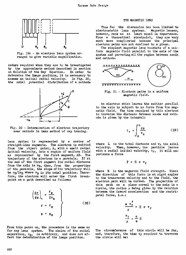
Vacuum Tube Design
#2 #3
Fig. 19c - An electron lens system ar-ranged to give variable magnification.
cedure required when they are to be investigatedby the approximate method described in sectionon Solution of the Ray Equation. In order todetermine the image position, it is necessary toassume an initial radial velocity. In Fig. 20,the axial potential distribution of a cathode
-ZB re-.]
Fig. 20 - Determination of electron trajectorynear cathode in Gans method of ray tracing.
lens system is represented by a series of
straight-line segments. The electron is emittedfrom the object point, A, with a small radialinitial velocity, into a region of uniform fieldas represented by the first segment, AB. Thetrajectory of the electron is a parabola. If atthe end of the first segment its radial distancefrom the axis is rB, then, from the propertiesof the parabola, the slope of its trajectory willbe rB/2zB where zB is its axial position. There-fore, the electron will enter the first break-point on a path described as follows:
(dr-) =rB
dz 2 2ZB
r = rB
= cPB
(38)
From this point on, the procedure is the same asfor any lens system. The choice of the radialseparation, rB, is arbitrary, and does not af-fect the determination of the image position.
THE MAGNETIC LENS
Thus far the discussion has been limited toelectrostatic lens systems. Magnetic lenses,however, rank as at least equal in importance.From a theoretical standpoint, they are verymuch more complicated because the principalelectron paths are not confined to a plane.
The simplest magnetic lens consists of a uni-form magnetic field parallel to the axis of thesystem and pervading all the region between anodeand cathode.
0 0 0 0 0 0 0 0 0 0 0 0 0 0 0
0 0 0 0 0 0 0 0 0 0 0 0 0 0 0 0
Fig. 21 - Electron paths in a uniformmagnetic field.
An electron which leaves the emitter parallelto the axis is subject to no force from the mag-netic field. The time required by this electronto traverse the distance between anode and cath-ode is given by the integral:
dt
z,. -
v0
where L is the total distancevelocity. When, however, thewith a radial initial velocity,perience a force
F = H e vr
(39)
and vz the axialparticle leavesvr, it will ex -
where H is the magnetic field strength. Sincethe direction of this force is at right anglesto the transverse velocity and to the field, theelectron path will be curved. The projection ofthis path on a plane normal to the axis is acircle, the radius p being given by the relationbetween the inward acceleration and the centri-petal force, i.e.:
2112 vr
p- H e vr
vr= H
The circumference of this circle will be 2Ap,and, therefore, the time t2 required to traversethe circle will be:
150
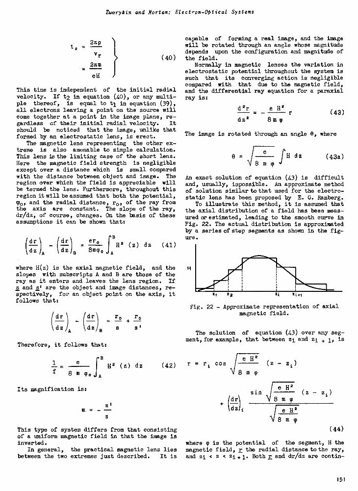
Zworykin and Morton: Electron-OPtical Systems
t 22np
vr2nm
eH
(40)
This time is independent of the initial radialvelocity. If t2 in equation (40), or any multi-ple thereof, is equal to t1 in equation (39),all electrons leaving a point on the source willcome together at a point in the image plane, re-gardless of their initial radial velocity. It
should be noticed that the image, unlike thatformed by an electrostatic lens, is erect.
The magnetic lens representing the other ex-treme is also amenable to simple calculation.This lens is the limiting case of the short lens.Here the magnetic field strength is negligibleexcept over a distance which is small comparedwith the distance between object and image. Theregion over which the field is appreciable willbe termed the lens. Furthermore, throughout thisregion it will be assumed that both the potential,To, and the radial distance, ro, of the ray fromthe axis are constant. The slope of the ray,dr/dz, of course, changes. On the basis of theseassumptions it can be shown that:
dr dr(dz )A dzB
ero8nupo fA
H2 (z) dz (41)
where H(z) is the axial magnetic field, and theslopes with subscripts A and B are those of theray as it enters and leaves the lens region. Ifs and s' are the object and image distances, re-spectively, for an object point on the axis, itfollows that:
(dz dr -dr
(dz )A B
Therefore, it follows that:
ro+
ro
s s'
1 H2 (z) dz (42)f 8 m cpo
Its magnification is:
stM = - -s
This type of system differs from that consistingof a uniform magnetic field in that the image isinverted.
In general, the practical magnetic lens liesbetween the two extremes just described. It is
capable of forming a real image, and the imagewill be rotated through an angle whose magnitudedepends upon the configuration and magnitude ofthe field.
Normally in magnetic lenses the variation inelectrostatic potential throughout the system issuch that its converging action is negligiblecompared with that due to the magnetic field,and the differential ray equation for a paraxialray is:
der e H2
dz2 8 m cp(43)
The image is rotated through an angle 0, where
=e dz (43a)
8 m y
An exact solution of equation (43) is difficultand, usually, impossible. An approximate methodof solution similar to that used for the electro-static lens has been proposed by E. G. Ramberg.
To illustrate this method, it is assumed thatthe axial distribution of a field has been meas-ured ar estimated, leading to the smooth curve inFig. 22. The actual distribution is approximatedby a series of step segments as shown in the fig-ure.
H
22 it
Fig. 22 - Approximate representation of axialmagnetic field.
The solution of equation (43) over any seg-ment, for example,
r = ri cos
that between zi and zi 1, is
e H2 (z - zi)8 m p
e H2
(dr(z - zi)sin \I
8 m p
dz)i e H2
8 m p(44)
where p is the potential of the segment, H themagnetic field, r the radial distance to the ray,and zi < z < zi + 1. Both r and dr/dz are contin-
151
Vacuum Tube Design
uous at the break-points, so that the solutionsfor the individual segments given by equation (44)join smoothly.
With the aid of the initial conditions, thesubstituted field distribution, and equation(44), the path of the ray (or, more exactly, theradial displacement), can be traced through thelens just as is done for the electrostatic sys-tem. Two ray paths are sufficient to determinethe first -order -image properties of the magneticlens.
Finally, considering the most general casewhere the lens action is due both to magneticand electrostatic fields, the differential rayequation becomes:
der 1 dr dcp -dz2 2 p dz dz r
(1 d2c17
4 p dz2 eH2)8 rum
where the symbols have the previously assignedmeanings. The rotation of the image is given by
dz
8 m
REFERENCES
1. E. BrUche and O. Scherzer, "Elektronenop-tik," Julius Springer, Berlin, 1934.
2. H. Busch and E. Bruche, "Beitrlige zur Elek-tronenoptik," J. A. Barth, Leipzig, 1937.
3. I. G. Maloff and D. W. Epstein, "ElectronOptics in Television," McGraw-Hill Book Com-pany, Inc., New York, 1938.
4. H. Busch, "Cathode Ray Paths in AxiallySymmetric Fields," Ann. Physik, Vol. 81,pp. 974-993; 1926.
5. M. Knoll and E. Ruska, "Geometric ElectronOptics," Ann. Physik, Vol. 12, No. 5, pp.607-640, 641-661; 1932.
6. J. Picht, "Theory of Geometric Optics forElectrons," Ann. Physik, Vol. 15, No. 8,pp. 926-964; 1932.
7. E. Bruche, "Fundamentals of GeometricalElectron Optics," Z. tech. Physik, Vol. 14,No. 2, pp. 49-58; 1933. See, also, Z. Phy-sik, Vol. 78, No. 1-2, pp. 26-42; 1932.
8. O. Scherzer, "Theory of Electric ElectronCondensing Lenses," Z. Physik, Vol. 80, No.3-4, pp. 193-202; 1933.
9. W. Glaser, "Geometrical Optics of ElectronRays," Z. Physik, Vol. 80, No. 7-8, pp.
451-464; 1933.
10. V. K. Zworykin, "Electron Optics," J.Frank-lin Inst., Vol. 215, pp. 535-555; 1933.
11. O. Scherzer, "Errors of Electron Lenses,"Z. Physik, Vol. 101, No. 9-10, pp. 593-603;1936.
12. W. Rogowski, "Aberrations of Electron Im-ages," Arch. Elektrotech., Vol. 31, No. 9,pp. 555-593; 1937.
14
L. H. Bedford, "Electron Lens Formulas,"Phys. Soc. Proc.,Vol. 46, pp.882-888; 1934.See, also, C. J. DavissonandC. J. Calbick,Phys. Rev., Vol. 38, p. 585; 1931: and Vol.42, p. 580; 1932.
R. Gans, "Electron Paths in Electron Op-tics," Z. Tech. Physik, Vol. 18, No. 2, pp.41-48; 1937.
15. L. S. Polotovski, "Studies on Electron Op-tical Systems," Izveztia Electroprom. Slab -ono Toka, No. 5, pp. 22-35, and No. 6, pp.13-27; 1934.
16. D. W. Epstein, "Electron Optical Systems ofTwo Cylinders," Proc. I. R. E., Vol. 24,No. 8, pp. 1095-1139; 1936.
17. G. A. Morton and E. G. Ramberg, "ElectronOptics of an Image Tube," Physics, Vol. 7,No. 12, pp. 451-459; 1936.
18. E. G. Ramberg, "Simplified Derivation ofGeneral Properties of an Electron OpticalImage," J. Optical Soc. Am., Vol. 29, pp.79-83; 1939.
19. W. Henneberg and A. Recknagel, "ChromaticErrors of Electron Optical Systems," Z.tech. Physik, Vol. 16, No. 8, pp. 230-235;1935.
20. E. Gundert, "Demonstration of the Aberra-tions of Electron Lenses," Physik. Z., Vol.38, No. 12, pp. 462-467; 1937.
21. B. von Borries and E. Ruska, "Electron Su-per Microscope," Wiss. Veroffentl. Siemens-werke, Vol. 17, No. 1; 1938.
152
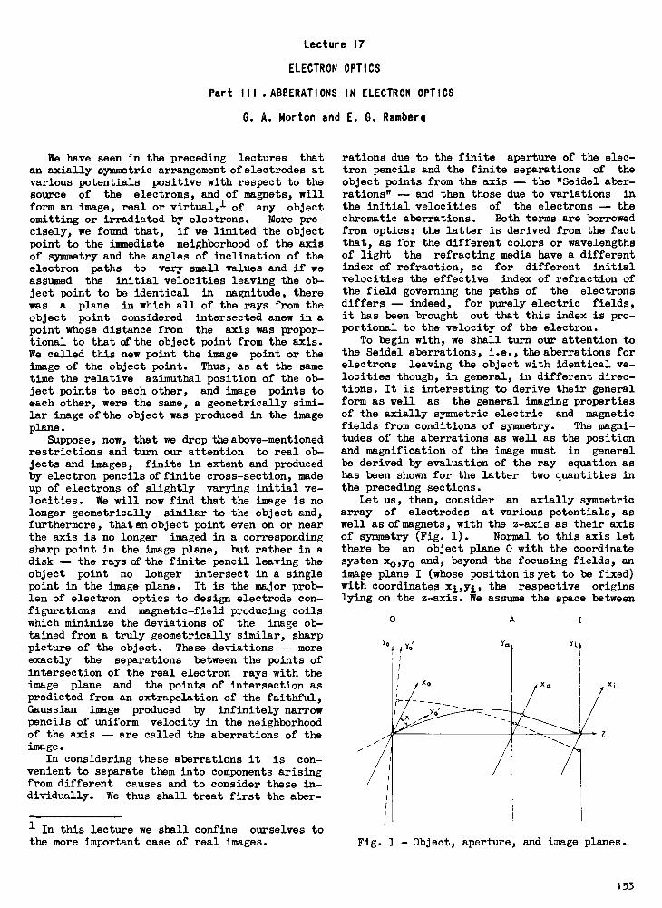
Lecture 17
ELECTRON OPTICS
Part III . ABBERATIONS IN ELECTRON OPTICS
G. A. Morton and E. G. Ramberg
We have seen in the preceding lectures thatan axially symmetric arrangement of electrodes atvarious potentials positive with respect to thesource of the electrons, and of magnets, willform an image, real or virtual,1 of any objectemitting or irradiated by electrons. More pre-cisely, we found that, if we limited the objectpoint to the immediate neighborhood of the axisof symmetry and the angles of inclination of theelectron paths to very small values and if weassumed the initial velocities leaving the ob-ject point to be identical in magnitude, therewas a plane in which all of the rays from theobject point considered intersected anew in apoint whose distance from the axis was propor-tional to that of the object point from the axis.We called this new point the image point or theimage of the object point. Thus, as at the sametime the relative azimuthal position of the ob-ject points to each other, and image points toeach other, were the same, a geometrically simi-lar image of the object was produced in the imageplane.
Suppose, now, that we drop the above -mentionedrestrictions and turn our attention to real ob-jects and images, finite in extent and producedby electron pencils of finite cross-section, madeup of electrons of slightly varying initial ve-locities. We will now find that the image is nolonger geometrically similar to the object and,furthermore, that an object point even on or nearthe axis is no longer imaged in a correspondingsharp point in the image plane, but rather in adisk -- the rays of the finite pencil leaving theobject point no longer intersect in a singlepoint in the image plane. It is the major prob-lem of electron optics to design electrode con-figurations and magnetic -field producing coilswhich minimize the deviations of the image ob-tained from a truly geometrically similar, sharppicture of the object. These deviations -- moreexactly the separations between the points ofintersection of the real electron rays with theimage plane and the points of intersection aspredicted from an extrapolation of the faithful,Gaussian image produced by infinitely narrowpencils of uniform velocity in the neighborhoodof the axis -- are called the aberrations of theimage.
In considering these aberrations it is con-venient to separate them into components arisingfrom different causes and to consider these in-dividually. We thus shall treat first the aber-
1 In this lecture we shall confine ourselves tothe more important case of real images.
rations due to the finite aperture of the elec-tron pencils and the finite separations of the
object points from the axis -- the "Seidel aber-rations" -- and then those due to variations in
the initial velocities of the electrons -- thechromatic aberrations. Both terms are borrowedfrom optics: the latter is derived from the factthat, as for the different colors or wavelengthsof light the refracting media have a differentindex of refraction, so for different initialvelocities the effective index of refraction ofthe field governing the paths of the electronsdiffers -- indeed, for purely electric fields,it has been brought out that this index is pro-portional to the velocity of the electron.
To begin with, we shall turn our attention tothe Seidel aberrations, i.e., the aberrations forelectrons leaving the object with identical ve-locities though, in general, in different direc-tions. It is interesting to derive their generalform as well as the general imaging propertiesof the axially symmetric electric and magneticfields from conditions of symmetry. The magni-tudes of the aberrations as well as the positionand magnification of the image must in generalbe derived by evaluation of the ray equation ashas been shown for the latter two quantities inthe preceding sections.
Let us, then, consider an axially symmetricarray of electrodes at various potentials, aswell as of magnets, with the z-axis as their axisof symmetry (Fig. 1). Normal to this axis letthere be an object plane 0 with the coordinatesystem xo,yo and, beyond the focusing fields, animage plane I (whose position is yet to be fixed)with coordinates xi,yi, the respective originslying on the z-axis. We assume the space between
0 A
Fig. 1 - Object, aperture,
xL
and image planes.
153
Vacuum Tube Design
0 and I to be free from matter(space charge neg-ligible), so that Laplace's equation holds forboth the electric and the magnetic field, andfurthermore, that the space surrounding the planeI is field -free. We now introduce between 0 andI, also normal to the z-axis, an "aperture plane"A with coordinates xa,ya -- close enough to Ithat the entire space between A and I may be re-garded as field -free. We give the same orienta-tion to the several coordinate systems, so that,e.g., the xo-, xa- and xi -axes are coplanar andparallel.
Suppose now that electrons leave variouspoints of the object plane, throughout with thesame absolute velocity, though generally in dif-ferent directions. If we fix our attention onone such electron leaving the point x0,y0 in theobject plane and aimed so that it passes throughthe point xa,ya of the aperture plane, its pathwill, in view of the fixed field conditions, be
uniquely determined and accordingly also its in-tersection xi,yi with the image plane. Hence wemay regard the coordinates xi and yi as functionsof the coordinates of the ray in the object and
aperture planes, xopYopra, and Ya; and, in viewof the continuity of the force fields to whichthe electrons are subjected, express them in termsof apower series of these latter four coordinates,such as
xi = a, + alx + azy + azxa + a4ya +2 2
a,x0 + a6x0y0 + a,y, +
azxoxa + . (1)
There is a similar expression, with different co-efficients, for yi. We will see that we cansimplify these expressions very considerably bymaking use of the symmetry conditions of theproblem. We must here satisfy the obvious re-quirement that, if we rotate the radius vectorsto the ray intersections in planes 0 and A throughany given angle q, the corresponding intersectionin plane I is found by rotating the radius vector
to xi,yi through the same angle p. Thus equa-tion (1) must remain satisfied if we carry outthe simultaneous substitution:
x cos p - yisin
x0-1-xocos p - yosin
Xa-0.X aCOS p - yaSin
y0-4-x0sin
ya -*xasin
p
p
p (2)
p + yocos p
P + yacos P
Putting p = 1800 simply changes the sign of allthe coordinates and we obtain
-xi = a, - atx, - azy, - azxa - a4ya +
2 2azx + a6x0y0 + aiy +
azx,xa + . .
Adding equation (1), we find that the sum of allthe terms of even order in the coordinates mustvanish:
2 20 = 2a0 + 2azx + 2a6x0y0 + 2a7y, +
2asxoxa + .
As this must be true for all values in a contin-uous range of xo, yo,xa,ya, all the coefficientsof the terms of even order ao, a5, a6, a7, as...must vanish individually and we are left withterms in the first, third, fifth ... order in thecoordinates. If we confine our attention to re-gions of the object very close to the axis andelectron rays leaving these which, also, strikethe aperture plane very close to the axis (i.e.,imaging pencils of very small aperture), we gainsufficient information regarding the pattern inthe image plane if we consider the terms of thefirst order only. Let us, then, substitute equa-tion (2) in equation (1) with p left arbitrary.As the resulting equation must be valid for allvalues of p, it must be fulfilled by the coeffi-cients on the two sides of the equation of cos pand sin y individually. Hence, we obtain
x:1)= aix, + azy, + azxa + a4ya
(ayi) = - azz + 0.0'0 - a,ora + a3ya
(3)
the superscript (1) indicating that the expres-sions constitute an approximation taking accountof the first -order terms only.
Consider now a ray leaving the point xo = 0,yo = 0 and passing through xa = c, ya = 0. Forit we have
x(1)= aze
(4)I)
yi = - a4c
Now the only tangential forces which the electronundergoes arise from the action of the magneticfield. According to Larmor's theorem its angularvelocity about the axis is, however, equal toeHz/(2m), where Hz is the longitudinal componentof the magnetic field at the point of observa-
154
Morton and Ramberg: Abberations in Electron Optics
tion.2 As, however, Hz = 0 in the aperture planeand beyond, the angular velocity of the electronmust here be zero throughout. The path of theelectron between the aperture and image planesis thus a straight lime proceedingina meridionalplane -- in our example in the zx-plane. Hence,
in (4),
yi(1)= 0 and, as c # 0 , a4 = 0
We now take one more step: the ray in thezx-plane which we are considering will, in gen-eral be inclined to the axis of symmetry. Let us,hence, follow it to its point of intersection withthe axis and fix the image plane I as the planenormal to the axis passing through this point.3With this choice of I, we have xi= 0 and hencealso a3 = O. Thus we obtain finally:
(1)xi = a,,xo + a,y, = pxot
(5)
sr1) - azxo + aiyo = Oyo
where
2 If we introduce the polar coordinates r, T, theexact integration of Newton's equation for the(p -direction
dt---(mr20 = re (iH - iHr)
taking account of Laplace's equation
H =-='(rH ) = 0
az r ar r
yields
r2 = [r2 ci)] z=o[Hz r2
m 2
8 (are r=0 72 "ar4 r=00
a2H a4H1 Z r4 1 Z r6
This vanishes, if r = 0 at z = 0, in any planein which Hz= 0.
3 Our original assumptions regarding the imageplane I are equivalent to postulating that thispoint fall into the field -free space beyond thefocusing fields.
xo = xocos x - yosin x
yo = xosin x + yoeos x
x = arctan (-
2 2
0 = (a1 + a2)2
at(6)
x' yl are the coordinates of the object pointos oreferred to a coordinate system rotated withrespect to the original one (and the systemsin planes A and I) through the angle X. Wethus have the final result that, to a firstapproximation in the coordinates of the ob-ject and aperture planes, all the rays leav-ing any point in the object plane 0 are re-united in a point in the image plane I. Fur-thermore, to any array of object points therecorresponds a geometrically similar array ofimage points with separations magnified, orreduced, by the factor 0 and rotated, onerelative to the other, through the angle x.In short, to a first approximation, our ax-ially symmetrical field combination gives a
sharp and faithful "Gaussian" image of the ob-ject.
For purely electric fields (as for an or-dinary optical lens system), the angle x van-ishes, as rays starting in a given meridionalplane do not leave this plane. Owing to thefact that in this case all of the forces actingon the electron are radial or axial, the rela-tion (1) must remain true if we reflect all ofthe coordinates at any meridional plane, e.g.,change the signs of the x -coordinates and leavethose of the y -coordinates unchanged (reflec-tion at the yz -plane). This requirement leadsto a2 = 0, and hence x = O.
If we drop the assumption of an image fieldof infinitesimal extent and imaging pencilsof infinitesimal aperture, we must take intoconsideration the terms of higher order inthe expressions for xi and yi -- they informus of the deviations of the real image fromthe Gaussian sharp and geometrically faith-ful image -- the aberrations. For many pur-poses, if the image field and apertures arenot too large, it is sufficient to restrictour attention to the terms of the third order.We obtain, then, the so-called third -order(Seidel) aberrations. Thus, we may write, giv-ing a new meaning to the coefficients al, a2,a3, a4,
155
Vacuum Tube Design
a 2
Axi = aixa + apcaya +
2 3a3XaYa a4y,
Aperture Defect(SphericalAberration)
2 1
+ + b2x0xay. +
1 2bsxoy. + b4yox. + Coma
t 2
b070Xaya + b631057a
21+ CXX
1 0 a
21
C2X0 ya
I I
CsX0370XaI 1
e4X01707a2
12 t2core, x. + csy, y.
3 21 1 1
+ dix, + d2xo yo +
1 1
2
d2x0y,3
1
+ d4y0
(7)
Curvatureof
Fieldand
Astigma-tism
Distortion
and a similar expression for Ayi. Axi and AYiare the third -order deviation of the ray inter-section with the image plane from the correspond-ing first -order, Gaussian, intersection or imagepoint:
(a)
xi Xi(a) + 0x1 ; Sri(al= 37i(i) + 61ri.
For convenience we now refer our object planecoordinates to the rotated (primed) coordinatesystem. To the right of every group of termsinvolving the same power of the coordinates ofthe object plane and of the coordinates of theimage plane, we have written down the customarydesignation of the corresponding aberration.Their origin will become evident later.
An application of our symmetry condition willshow that the twenty coefficients in equation (7)and the further twenty coefficients in the corre-sponding expression Ayi are by no means independ-ent. Let us, then, substitute equation (2) inequation (7) and satisfy the resulting equationindividually for the coefficients of sin p, cos y,sin3y, and cos3p. Expressing the coefficients interms of each other as far as the resulting re-lations permit, we find:
2 2 2 2
Axi = aiXa(Xa+Ya) + a2y,(x,+y,)
t 2 2 1
+ 1),X0(xa+ya) + b5ya(yoxa-xoya) +
1 2 7b2y.(xox.+37,57.) + b4yo(xa+y.)
1 1 1
C,X0(X0Xa+3,037a) + C5370(YoXa-
1 1 1
xoya) + coo(xox.+yoy.) +
2 2
c2Ya(xo +Yo )
2 2 2 2I 1 1 1
+ dixo(xo +yo ) + d2yo(xo +yo )
(8)2 2 2 2
Ayi = - a2xa(xa+ya) + aiya(xa+ya)
2 2 1
- b4X0(Xa+ya) - 105Xa(YolCa-XoYa) -
I 2 2102Xa(X0Xa+Yoya) + biyo(x.+y.)
1 1 1 I 1
ciYo(xoxa+YoYa) C5X0(YOXa-1 1 I 1
XoYa) - C3X0(X0Xa+Yoya)
1 1
2 2
C2xa(x0 +370 )
1 2 22 2
- d2xo(x, +yo ) + diyo(xo +yo )
If we again consider a ray leaving the pointon the axis in the object plane (xl) = 4 = 0)and passing through the point (xa = c, ya = 0),
Larmorts theorem tells us that the ray must pro-ceed in the zx-plane between A and I and thatthus' Ayj=0 and hence a2 = 0. We have thus re-duced the number of independent third -order coef-ficients to 11. For purely electric fields, inwhich case, as we have mentioned, the relationsmust hold if we reflect the coordinates at anymeridional plane, we have in addition b2 = b4 =c3 = c2 = d2 = 0, so that the number of independ-ent coefficients reduces to 6. To reduce them totheir true number, i.e., 8 for mixed and 5 forpurely electric fields, we must introduce a newfactor into our considerations. We may derivethis final simplification if we postulate theexistence of a wave -surface -- i.e., a continuoussurface normal to all the rays of a pencil orig-inating in one particular object point -- whichthe central ray of the pencil intersects in theaperture plane. Let the equation of this wave -surface be f(x,y,z) = 0. The direction cosinesof the normal at any point of the surface, coin-ciding with an electron ray intersecting the im-age planein the point (xi, yi, zi),will be given
by
of
By
[(xi -x)2 + (yi-y)2 + (z -z)12
(Y1 -Y)
of [(xi -x)2 + (yi-y)2 + (zi-z)212Bs
(9)
156
Horton and Ramberg: Abberations in Electron Optics
As we shall see further on, the gradient of/asof the wave -function f is a constant in a field -free space; furthermore, as the inclinations ofthe rays to the axis are assumed to be small, wemay replace the root in the denominator on theright by the constant Z = zi - za. Differen-tiating, we then find
17f2 2
-- 0(Xa+57a)
b4--[xo(xa+Y.)3
+ 2ya(xiox,+y'oa)J -
2 2 , t
+ 2ya(xoya-yoxa)
a2f a xi ax.1 2 2
ya(X0 +y, ) -- C+
ax BY ay.637a
(10)2 2
a2f aYi ayi2 2y.(x:-y0) - 2x,'ylox.
[
+
ay ax- c c
ax aXa
as xa and ya differ only in the second order 2 2I I I I
from the corresponding coordinates x and y of C2 Xa(Xo -y, ) 4' 2)(07037a
[
]
the wave -surface. If the wave -surface, or the
function f, exists, the two second derivativesappearing in equations (10) must be equal and weobtain as final condition
axi vaY
asraax
a
In view of the approximations made in its deri-vation, this condition applies only as long as werestrict the terms in xi and yi to those of thefirst and third order in the object and aperturecoordinates.
Applying equation (11) to equation (8) we ob-tain, finally:
2 2I I I
+ diyo(xo +y, ) -I 12
2
d2xo(xo +yo )
We shall now consider the component aberra-tions individually, and introduce polar coordi-nates
x, = ro cos yo
yo = ro sin yo
x. = ra cos y.
y. = ra sin cpa
to facilitate the discussion.
2 2
AXi = aiXa(Xa+Ya)If we consider an object point on the axis,
the only aberration arising is the so-calledaperture defect or spherical aberration:
b t 2 2 3
X0(Xa+Ya) 2x.(xox.+yoy.)] + Axi= aira cos cp.
3 3 (13)Ayi= aira sin y.
b4 2 2
3
yo(x.+y.) - 2x.(xoy.-ylox.)] The rays passing through a circular zone of theaperture plane with a radius equal to ra pass
2 2 (ci-Cs)]x.(xo +yo ) +
2 2
2 2I I
Xa(XP -Y; ) + 2x0YoYa[
+
[
2 2I
C2 Ya:(X0 -Y0 ) -
2 2
+ dixo(x, +yo )
2 2Ayi = alya(xa+ya)
I
2xoyox,I ]
2 2
+ d2yo(xo +yo )
through a second
2
Ax.
circular zone in the image plane
2
+ AYi =3
(air.) (13')
2
whose radius is proportional to the cube of ra.Fig. 2 is taken from a paper by Diels and Wendt.4At the top it shows the origin of the aperture de -feet in a lens, and below this, beam cross-sectionpatterns obtained experimentally at the positions1, 2, and 3 relative to a magnetic electron lensimaging a point source. The upper row was ob-tained with a pencil of small aperture; the lower
(12) 4 K. Diels and G. Wendt, "Die 8Bildfehler dritterOrdnung Magnetischer Elektronenlinsen,"Zeits. f.techn. Physik," Vol. 18, No.3, p. 65; 1937.
157

Vacuum Tube Design
one with one of large aperture. The aperture de-fect arises from the fact that the marginal raysare bent more strongly toward the axis and cutthe axis at points between the lens and the imageplane. In the presence of this aberration, wesee from the figure that the sharpest image isobtained at a point between the lens and theGaussian image plane (position 3).
Fig. 2 - Aperture defect.(K. Diels and G. Wendt, reference 4)
The terms containing the aperture coordinatesin the second and those of the object plane inthe first power lead to another aberration, knownas coma. It is the aberration which, togetherwith the spherical aberration already described,affects primarily points lying only little offthe axis, but imaged with rather large aperturepencils. For purely electric fields we find forpoints lying on the yo -axis of the object plane,
biAxi = -rora sin 2pa
3
b1Ayi = -rare( 2 - cos 2cps
3
or, for an aperture zone of radius ra:
px2
+
22birer.
2
AYi -3
Fig. 3a - Coma.
the Gaussian image point (Fig. 3a). The super-position of these circles together with the spher-ical aberration giving the vertex of the 600 sec-tor a diffuse appearance results in the comet -
like structure shown in the upper middle photo -
Fig. 3b - Coma and astigmatism.(K. Diels and G. Wendt, reference 4)
graph in Fig. 3b.4 In the presence of a magneticfield (b4 # 0), the aberration figure (equation
(14) ]4') is merely changed in scale and rotatedabout the Gaussian image point through the anglearc tan (b4/101):
(14')
For aperture zones of increasing radius, thiscorresponds to a series of circles enclosed bytwo lines at 300 to the y-axis intersecting at
2Qxi ror
2AYI = rot'.
[blsin 2pa+ b4( 2 + cos 2cpa)j
3
(15)
[b1( 2 - cos 2(pa) + b4 sin 2cpa]
3
4 Loc. cit.
158
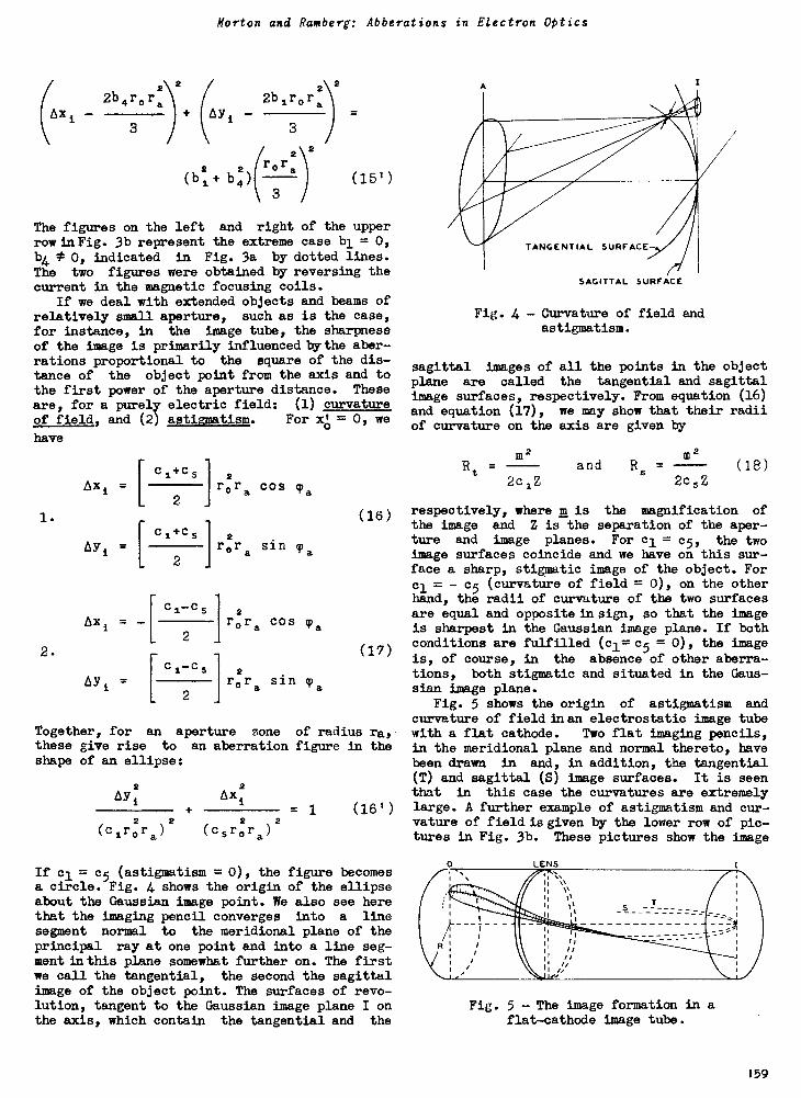
Horton and Ramberg: Abberations in Electron Optics
2h4rorf\2 2bir2
AY i
3 3
2 2 ro r a(bi+ b4)
(
3 /
2
(15 ' )
The figures on the left and right of the upperrow in Fig. 3b represent the extreme case bl = 0,b4 # 0, indicated in Fig. 3a by dotted lines.
The two figures were obtained by reversing thecurrent in the magnetic focusing coils.
If we deal with extended objects and beams ofrelatively small aperture, such as is the case,for instance, in the image tube, the sharpnessof the image is primarily influenced by the aber-rations proportional to the square of the dis-tance of the object point from the axis and tothe first power of the aperture distance. Theseare, for a purely electric field: (1) curvatureof field, and (2) astigmatism. For x, = 0, we
have
[ C1+ c52
Axi = rora cos pa2
1. (16)cs+c,
AY = rora sin pa2
PxC 5 2
rora cos pa2
2. (17)
=
c1 -c5 2
pyi2
rare. sin pa
Together, for an aperture zone of radius ra,these give rise to an aberration figure in theshape of an ellipse:
2AY i
2 2(C irora )
2AX
2 2(c,rora)
( 16 ' )
If ca. = 05 (astigmatism = 0), the figure becomesa circle. Fig. 4 shows the origin of the ellipseabout the Gaussian image point. We also see herethat the imaging pencil converges into a linesegment normal to the meridional plane of theprincipal ray at one point and into a line seg-ment in this plane somewhat further on. The firstwe call the tangential, the second the sagittalimage of the object point. The surfaces of revo-lution, tangent to the Gaussian image plane I onthe axis, which contain the tangential and the
TANGENTIAL SURFACE
SAGITTAL SURFACE
Fig. 4 - Curvature of field andastigmatism.
sagittal images of all the points in the objectplane are called the tangential and sagittalimage surfaces, respectively. From equation (16)and equation (17), we may show that their radiiof curvature on the axis are given by
m2Rt =
2c iZ
and2
/13
R. =2c5Z
( 18 )
respectively, where m is the magnification ofthe image and Z is the separation of the aper-ture and image planes. For el = 05, the twoimage surfaces coincide and we have on this sur-face a sharp, stigmatic image of the object. Forcl = - c5 (curvature of field = 0), on the otherhand, the radii of curvature of the two surfacesare equal and opposite in sign, so that the imageis sharpest in the Gaussian image plane. If bothconditions are fulfilled (ci=c5 = 0), the imageis, of course, in the absence of other aberra-tions, both stigmatic and situated in the Gaus-sian image plane.
Fig. 5 shows the origin of astigmatism andcurvature of field in an electrostatic image tubewith a flat cathode. Two flat imaging pencils,in the meridional plane and normal thereto, havebeen drawn in and, in addition, the tangential(T) and sagittal (S) image surfaces. It is seenthat in this case the curvatures are extremelylarge. A further example of astigmatism and cur-vature of field is given by the lower row of pic-tures in Fig. 3b. These pictures show the image
Fig. 5 - The image formation in aflat -cathode image tube.
159
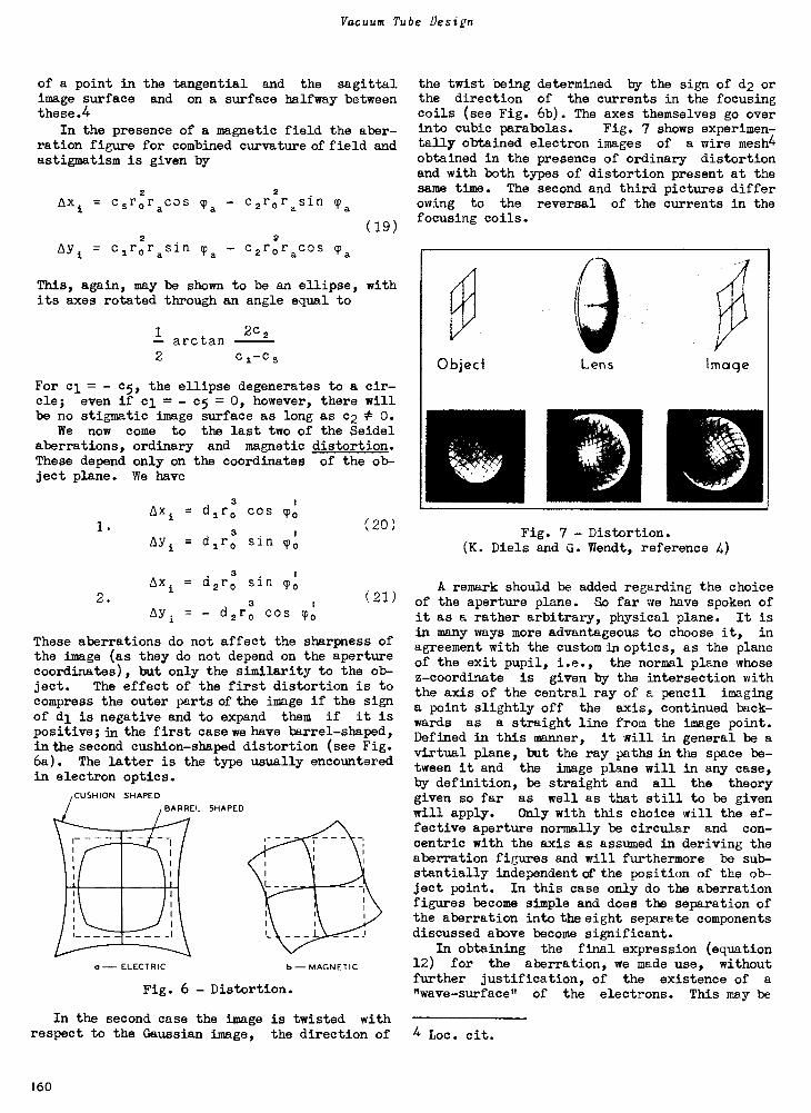
Vacuum Tube Design
of a point in the tangential and the sagittalimage surface and on a surface halfway betweenthese.4
In the presence of a magnetic field the aber-ration figure for combined curvature of field andastigmatism is given by
©x12 2
csr0racos (pa - c,r0rasin
(19)2 2
AYi = cirorasin Ta - c,roracos T.
This, again, may be shown to be an ellipse, withits axes rotated through an angle equal to
1
2
arc tan2c2
1 -C 5
For ci = - c5, the ellipse degenerates to a cir-cle; even if ci = - c5 = 0, however, there willbe no stigmatic image surface as long as c2 * O.
We now come to the last two of the Seidelaberrations, ordinary and magnetic distortion.These depend only on the coordinates of the ob-ject plane. We have
AXi =3
air, cos To1.
3(20)
AYi = diro sin To
3AXi = d,r, sin To
2. 3 (21)= - d,r, cos To
These aberrations do not affect the sharpness ofthe image (as they do not depend on the aperturecoordinates), but only the similarity to the ob-ject. The effect of the first distortion is tocompress the outer parts of the image if the signof d1 is negative and to expand them if it ispositive; in the first case we have barrel -shaped,in the second cushion -shaped distortion (see Fig.6a). The latter is the type usually encounteredin electron optics.
CUSHION SHAPEDBARREL SHAPED
o - ELECTRIC b - MAGNETIC
Fig. 6 - Distortion.
In the second case the image is twisted withrespect to the Gaussian image, the direction of
the twist being determined by the sign of d2 orthe direction of the currents in the focusingcoils (see Fig. 6b). The axes themselves go overinto cubic parabolas. Fig. 7 shows experimen-tally obtained electron images of a wire mesh4obtained in the presence of ordinary distortionand with both types of distortion present at thesame time. The second and third pictures differowing to the reversal of the currents in thefocusing coils.
Fig. 7 - Distortion.(K. Diels and G. Wendt, reference 4)
A remark should be added regarding the choiceof the aperture plane. So far we have spoken ofit as a rather arbitrary, physical plane. It isin many ways more advantageous to choose it, in
agreement with the custom in optics, as the planeof the exit pupil, i.e., the normal plane whosez-coordinate is given by the intersection withthe axis of the central ray of a pencil imaginga point slightly off the axis, continued back-wards as a straight line from the image point.Defined in this manner, it will in general be avirtual plane, but the ray paths in the space be-tween it and the image plane will in any case,by definition, be straight and all the theorygiven so far as well as that still to be givenwill apply. Only with this choice will the ef-fective aperture normally be circular and con-centric with the axis as assumed in deriving theaberration figures and will furthermore be sub-stantially independent of the position of the ob-ject point. In this case only do the aberrationfigures become simple and does the separation ofthe aberration into the eight separate componentsdiscussed above become significant.
In obtaining the final expression (equation12) for the aberration, we made use, withoutfurther justification, of the existence of a
"wave -surface" of the electrons. This may be
4 Loc. cit.
160
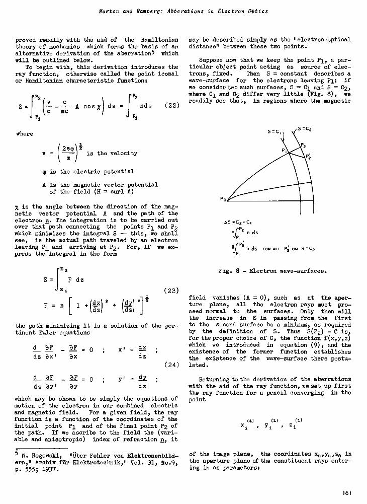
Morton and Ramberg: Abberations in Electron Optics
proved readily with the aid of the Hamiltoniantheory of mechanics which forms the basis of analternative derivation of the aberrations whichwill be outlined below.
To begin with, this derivation introduces theray function, otherwise called the point iconalor Hamiltonian characteristic function:
S =IP2v e- - A cos x) ds = nds (22)
c me
P2
1
where
1
(
i
2em)Tv = ---- is the velocity
m
m is the electric potential
A is the magnetic vector potentialof the field (H = curl A)
x is the angle between the direction of the mag-netic vector potential A and the path of theelectron s. The integration is to be carried outover that path connecting the points Pl and P2which minimizes the integral S -- this, we shallsee, is the actual path traveled by an electronleaving P1 and arriving at P2. For, if we ex-press the integral in the form
may be described simply as the "electron -opticaldistance" between these two points.
Suppose now that we keep the point P1, a par-ticular object point acting as source of elec-trons, fixed. Then S = constant describes awave -surface for the electrons leaving P1: if
we consider two such surfaces, S = C1 and S = C2,where C1 and C2 differ very little (Fig. 8), wereadily see that, in regions where the magnetic
a5 =C2 -c1
f P2n ds
rjP1
FOR ALL 1='; ON S =C2
S=
Z2
zi
F dz
Fig. 8 - Electron wave -surfaces.
(23)field vanishes (A = 0), such as at the aper-F=1n [ 1 4dz/k0 24. 14 2](
kdz/ture plane, all the electron rays must pro-ceed normal to the surfaces. Only then will
the path minimizing it is a solution of the per-tinent Euler equations
d aF aF = 0
dz ax' ax
xi = dx
dz
(24)
d aF "OF = 0 Y' = LIZ ;
dz 'a371 aY dz
which may be shown to be simply the equations ofmotion of the electron in our combined electricand magnetic field. For a given field, the rayfunction is a function of the coordinates of theinitial point P1 and of the final point P2 ofthe path. If we ascribe to the field the (vari-able and anisotropic) index of refraction n, it
5 W. Rogowski, "Uber Fehler von Elektronenbild-ern," Archly fur Elektrotechnik," Vol. 31, No.9,p. 555; 1937.
the increase in S in passing from the firstto the second surface be a minimum, as requiredby the definition of S. Thus S(P2) - C is,for the proper choice of C, the function f(x,y,z)which we introduced in equation (9), and theexistence of the former function establishesthe existence of the wave -surface there postu-lated.
Returning to the derivation of the aberrationswith the aid of the ray function, we set up firstthe ray function for a pencil converging in thepoint
(1) (i) (1)xi , Yi , zi
of the image plane, the coordinates x,,ya,za inthe aperture plane of the constituent rays enter-ing in as parameters:
161
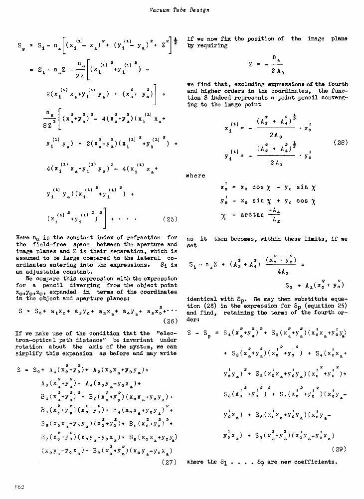
Vacuum Tube Design
[
2 : If we now fix the position of the image plane
Sp = Si- na (xi(1)2
(1) 2- x.) + (ST,._ ya )+ Z by requiring
na(1)
2(1)
2
= naZ2Z
kxi +Yi
2(3(14) xa+yi(1) y a)2
+ (Xa+ Y28)1
na2 2 2 2 2
8Z3
(Xa+ya) 4(xa+ya)(x xa+
2 2y(a) y a) + 2(xa2+y2a)(xi(1) +3T1(a) ) +
(1) (1) 2, (1)
40[i xal-Yi 57 a) - LI(xi x.+
(1) 2 (I) 2Yi Ya)(xi ) +
2 2 2
(Xi +yi ) + (25)
Here na is the constant index of refraction forthe field -free space between the aperture andimage planes and Z is their separation, which isassumed to be large compared to the lateral co-ordinates entering into the expressions. Si isan adjustable constant.
We compare this expression with the expressionfor a pencil diverging from the object point
xopYopzo, expanded in terms of the coordinatesin the object and aperture planes:
2S = So+ aixo+ a2y0+ a,x.+ a4y.+ asxo+--
(26)
z= -n a
2 A3
we find that, excluding expressions of the fourthand higher orders in the coordinates, the func-tion S indeed represents a point pencil converg-ing to the image point
where
(A22 + A4)r
2 A 3
xo
12 2
(A2 A4)y
(a)yi Yo2 A3
X0
370 =
X =
xo cos x - yo sin x
xo sin x + Yo
-A4arctan
A2
cos X
(28)
as it then becomes, within these limits, if weset
Si - naZ
2 2
+ (A2 2 (Xo + yo)
s-2 + A4) =
4A3
2 2
So + A1(X0 + 370)
identical with S. We may then substitute equa-tion (28) in the expression for Sp (equation 25)and find, retaining the terms of the fourth or-der:
2 2 2 2 2
If we make use of the condition that the "elec- S - S = Si(xa+ya) + S2(Xa a 0 a 0+y )(x x +y y)a
tron-optical path distance" be invariant underrotation about the axis of the syst.m, we can 2 2
2 2
simplify this expansion as before and may write + S3(xa+ya)(xo +yo ) + S4(xoxa+
S= 2 2So+ A1(xo+yo)+ A2(xoxa+yoya)+
2 2A3(Xa+37a)+ A4(X0Ya-YoXa)+
2 2 2 2 2Bi(xa+ya) + B2(xa+ya)(xoxa+yoya)+
2 2 2 2 2
B3(Xa+Ya)(X0+370)+ B4(XoXa+yoya)
2 2 2 2 2
B5(X0Xa+5701ra)(X0+570)4. 86(X0+370)
2 2
B7(xo+yo)(xoya-yoxa)+ BE, (X0Xa+YoYa)
2 2(X0ya....Y0Xa)+ B3(Xa+Ya)(X017a-Y0X3)
(27) where the
2t 1 1
2 2
YoYa) + Ss(xoxa+YoYa)(x. +y. )+
2 2 2 2 2
S6(x0 +yo ) + S7(xo +yo )(xoy -a
Yoxa) So(xoxa+YoYa)(xoYa-
Yoxa) + S9(x:+y:)(x,;ya-yoxa)
(29)
Si . . . . S9 are new coefficients.
162
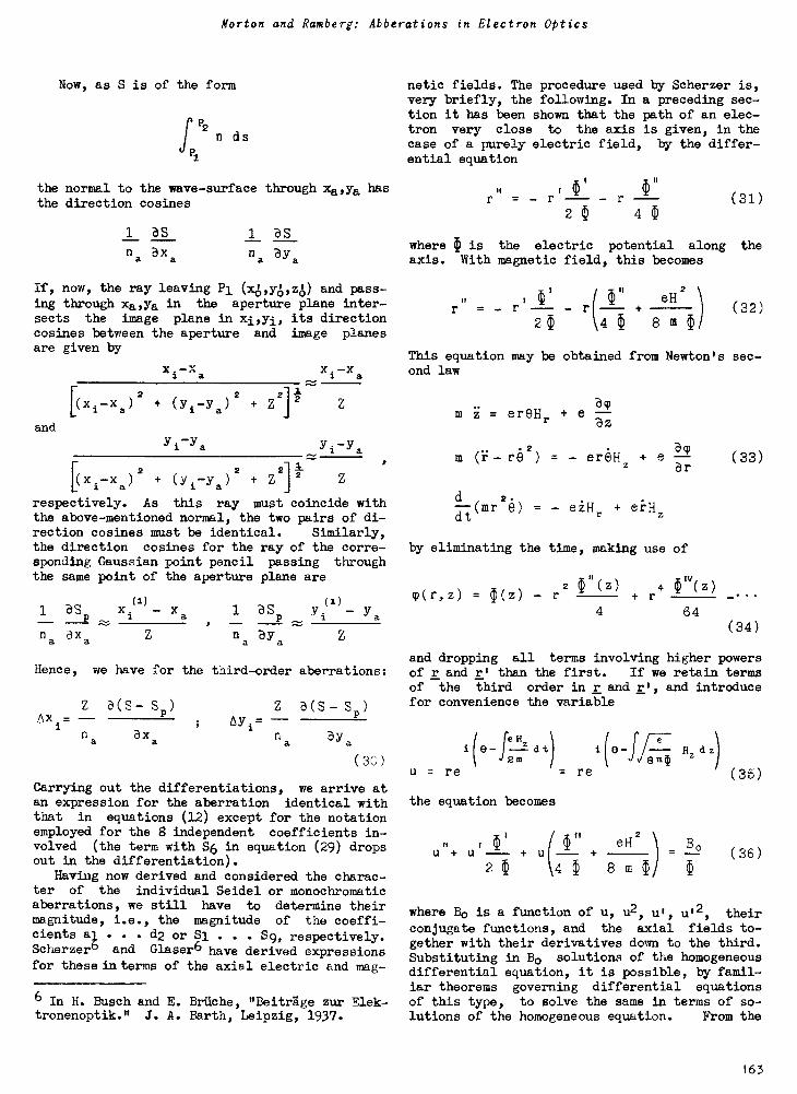
Morton and Ramberg: Abberations in Electron Optics
Now, as S is of the form
2n ds
1
the normal to the wave -surface through xa,ya hasthe direction cosines
1 as
na Bxa1 BS
n. By.
netic fields. The procedure used by Scherzer is,very briefly, the following. In a preceding sec-tion it has been shown that the path of an elec-tron very close to the axis is given, in thecase of a purely electric field, by the differ-ential equation
whereaxis.
r"11"- r - r (31)
2 (II 4 '1)
is the electric potential along theWith magnetic field, this becomes
If, now, the ray leaving P1 (x,!),y(1),z1)) and pass-
ing through xa,ya in the aperture plane inter- eH2(32)r - r
20- +
\al 8 Insects the image plane in xi,yi, its directioncosines between the aperture and image planesare given by
This equation may be obtained from Newton's sec-Xi -Xa xi -xa ond law
and
[(Xi-Xa)2 (YC'Ya)2 Z11 Zm z = ereff
r
By+ e --
Bz
Yi-Ya Yi-Yam re2) - erSH + e 22 (33)
ar2kx ._x ) (Yi-Ya)a
2
respectively. As this ray must coincide withthe above -mentioned normal, the two pairs of di- dt(mr26)
- eiHr + eiH
rection cosines must be identical. Similarly,the direction cosines for the ray of the corre- by eliminating the time, making use ofsponding Gaussian point pencil passing throughthe same point of the aperture plane are
(1)
1 -aS X -P
na axa
X 1 Sp Yi(1) ya-na Bya z
Hence, we have for the third -order aberrations:
Pxz a(s- Sp)
na ax
z a(s- sp)Ayi-
aBy,
(30)
Carrying out the differentiations, we arrive atan expression for the aberration identical withthat in equations (12) except for the notationemployed for the 8 independent coefficients in-volved (the term with S6 in equation (29) dropsout in the differentiation).
Having now derived and considered the charac-ter of the individual Seidel or monochromaticaberrations, we still have to determine theirmagnitude, i.e., the magnitude of the coeffi-cients al . . . d2 or Si . . . S9, respectively.Scherzer° and Glaser6 have derived expressionsfor these in terms of the axial electric and mag-
6 In H. Busch and E. BrUche, "BeitrKge zur Elek-tronenoptik." J. A. Barth, Leipzig, 1937.
Cr,z) = Um) - r2 r(z)
4
+ r4W(Z)
64(34)
and dropping all terms involving higher powersof r and r' than the first. If we retain termsof the third order in r and r', and introducefor convenience the variable
re Hi(0 -J
2mU = re
the equation becomes
U +
2
re
fi" eH2'I' +
4 '1 8 m
aZ d Zl/
(35)
Bo (36)
where Bo is a function of u, u2, u12, theirconjugate functions, and the axial fields to-gether with their derivatives down to the third.Substituting in Bo solutions of the homogeneousdifferential equation, it is possible, by famil-iar theorems governing differential equationsof this type, to solve the same in terms of so-lutions of the homogeneous equation. From the
163

Vacuum Tube Design
solutions can be derived the complete expressionsfor the aberrations. Scherzer has carried thisthrough and has given the expressions in a forminvolving derivatives of the electric potentialonly down to the second and of the magnetic fieldto the first. b°
The practical utilization of these expressionsand the general conclusions reached concerningtheir magnitude has been so far rather limited.In particular, it is of interest to know whichof these aberrations can be made to disappearentirely. An examination of the form of theseveral coefficients has shown here that:
1) Distortion and coma can be caused to van-ish completely, e.g., by making the magnification1:1, the electric potential symmetrical aboutthe midway plane between object and image, and
the magnetic field antisymmetrical about this
plane. In cases where the electrons start fromrest, as for instance in the image tube, thismethod is, however, of no value, as they would haveto arrive at the screen with zero energy as well.
2) Spherical aberration can be made to vanishunder no circumstances.7 The minimum sphericalaberration for weak electric and magnetic lenseshas been calculated by Scherzerg and by Rebschand Schneider.9 As weak lenses have little prac-tical interest, we shol, merely indicate their
general conclusions:a. The spherical aberration for weak elec-
tric and magnetic lenses is of the same order.In the optimum case, it is 20 per cent less forelectric than for magnetic lenses of equal aper-ture, focal length, and length.
b. The limit for immersion objectives and
magnetic lenses with image rotation is 1/9 aslarge as that for electric unit lenses (with thesame potential on object and image side) and mag-netic lenses without image rotation (compensatingcoils).
c. No improvement with respect to spher-ical aberration over either the electric or mag-netic lens can be obtained bycombining these two.
The spherical aberration of an electronlens consisting of two concentric cylinders hasbeen studied experimentally, in view of its greatimportance in connection with the production of
fine spots with electron guns, by Epstein10 and
6 Loc. cit.
7 O. Scherzer, "her einige Fehler von Elek-tronenlinsen," Zeits. f. Physik, Vol. 101, No.9 -
10, p. 593; 1936.
8 O. Scherzer, "Die Schwache Elektrische Einzel-linse Geringster Sphdrischer Aberration," Zeits.f. Physik, Vol. 101, No.1-2, p. 23; 1936.
9 R. Rebsch and W. Schneider, "Der offnungs -
fehler Schwacher Elektronenlinsen," Zeits. f.
Physik, Vol. 107, No.1-2; p. 138; 1937.
10 D. W. Epstein, "Electron Optical System of TwoCylinders as Applied to Cathode -Ray Tubes," Proc.I.R.E., Vol. 24, No.8, p. 1095; August, 1936.
Gundert.11 Epstein placed a diaphragm with aseries of apertures in the second anode cylinderand observed the image on a movable screen. He
measured out the separations of the spots due tothe outer apertures from the central spot. Usingtwo diameter ratios, 1.5 and 3.6, the larger onebeing at the higher potential, Epstein obtainedslightly better results with the ratio 3.6.
Gundert used the very different techniqueof introducing traces of gas into the tube -- hecould show that this did not affect his results
appreciably -- and photographing thread or gas -
focused rays which he directed by means of de-
flecting coils. He found that the sphericalaberration could be reduced considerably by mak-ing the second anode (at the higher potential)diameter smaller than that of the first anode.In this case, by bringing the marginal rays closeto the edge of the electrode in the negative por-tion of the lens, he found that they are here
refracted away from the axis so much more thanthe paraxial rays, that the excessive refractiontoward the axis in the positive portion of the
lens is partly compensated. Fig. 9 illustratesthis condition.
Fig. 9 - Aperture defect for cylinder lenses.
3) Curvature of field and astigmatism pres-
ent special problems. Ried112 has been able toshow that in the case of the electric weak shortunit lens the curvature and astigmatism cannotbe made to vanish for a plane object -- the tan-gential image is invariably concave toward the
lens. While this proof refers to a very limitedcase, all electron -optical systems considered sofar (except the uniform electric and magnetic
field types) appear to suffer to some extent from
11 E. Gundert, "Nachweis der Abbildungsfehler vonElektronenlinsen nach der Fadenstrahlmethode,"
Phys. Zeits., Vol. 38, No.12, P. 462; June, 1937.(Later papers contradict some of his conclusions.)
12 H. Riedl, "Die Bildfehler 3 Ordnung der KurzenSchwachen Rein Elektrischen Elektronen-Einzel -linse," Zeits.f.Physik, Vol. 107, p. 210; 1937.
164
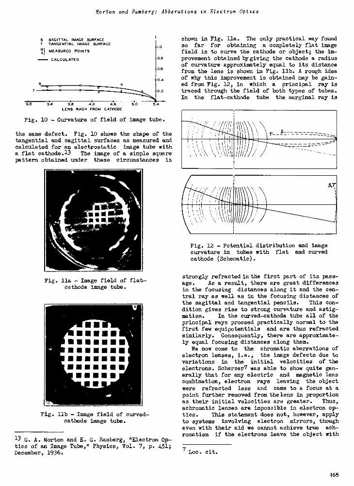
Norton and Ramberg: Abberations in Electron Optics
S SAGITTAL IMAGE SURFACET TANGENTIAL IMAGE SURFACEOt MEASURED POINTSxf
- CALCULATED
3A 3.6 4.2 4.6
LENS RADII FROM CATHODE5.0
1.0
0.6
0.6
0.4
0.2
5.4
Fig. 10 - Curvature of field of image tube.
the same defect. Fig. 10 shows the shape of thetangential and sagittal surfaces as measured andcalculated for an electrostatic image tube witha flat cathode.13 The image of a simple squarepattern obtained under these circumstances is
it I In
Fig. lla - Image field of flat -cathode image tube.
Fig. llb - Image field of curved -cathode image tube.
13 G. A. Morton and E. G. Ramberg, "Electron Op-tics of an Image Tube," Physics, Vol. 7, p. 451;December, 1936.
shown in Fig. lla. The only practical way foundso far for obtaining a completely flat imagefield is to curve the cathode or object; the im-provement obtained by giving the cathode a radiusof curvature approximately equal to its distancefrom the lens is shown in Fig. llb. A rough ideaof why this improvement is obtained may be gain-ed from Fig. 12, in which a principal ray istraced through the field of both types of tubes.In the flat -cathode tube the marginal ray is
Fig. 12 - Potential distribution and imagecurvature in tubes with flat and curvedcathode (Schematic).
strongly refracted in the first part of its pass-age. As a result, there are great differencesin the focusing distances along it and the cen-tral ray as well as in the focusing distances ofthe sagittal and tangential pencils. This con-dition gives rise to strong curvature and astig-matism. In the curved -cathode tube all of theprincipal rays proceed practically normal to thefirst few equipotentials and are thus refractedsimilarly. Consequently, there are approximate-ly equal focusing distances along them.
We now come to the chromatic aberrations ofelectron lenses, i.e., the image defects due tovariations in the initial velocities of theelectrons. Scherzer7 was able to show quite gen-erally that for any electric and magnetic lenscombination, electron rays leaving the object
were refracted less and came to a focus at apoint further removed from the lens in proportionas their initial velocities are greater. Thus,achromatic lenses are impossible in electron op-tics. This statement does not, however, applyto systems involving electron mirrors, thougheven with their aid we cannot achieve true ach-romatism if the electrons leave the object with
7 Loc. cit.
165
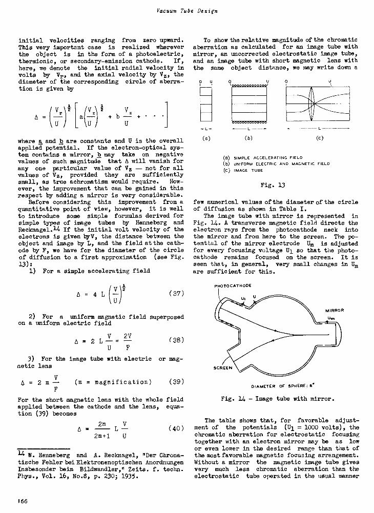
Vacuum Tube Design
initial velocities ranging from zero upward.
This very important case is realized whereverthe object is in the form of a photoelectric,thermionic, or secondary -emission cathode. If,
here, we denote the initial radial velocity involts by Vr, and the axial velocity by Vz, thediameter of the corresponding circle of aberra-tion is given by
Vr t Vz I VzA = (--- a --- + b --- +
U U U
where a and b are constants and U is the overallapplied potential. If the electron -optical sys-tem contains a mirror, b may take on negativevalues of such magnitude that A will vanish forany one particular value of Vz -- not for allvalues of Vz, provided they are sufficientlysmall, as true achromatism would require. How-ever, the improvement that can be gained in thisrespect by adding a mirror is very considerable.
Before considering this improvement from aquantitative point of view, however, it is well
to introduce some simple formulas derived forsimple types of image tubes by Henneberg andRecknage1.14 If the initial volt velocity of theelectrons is given by V, the distance between theobject and image by L, and the field at the cath-ode by F, we have for the diameter of the circleof diffusion to a first approximation (see Fig.
13):1) For a simple accelerating field
A = 4 L (
V)T--U
( 37 )
2) For a uniform magnetic field superposedon a uniform electric field
V 2VA = 2 L-- = - (38)
U F
3) For the image tube with electric or mag-netic lens
VA = 2 m (m = magnification) (39)
F
For the short magnetic lens with the whole fieldapplied between the cathode and the lens, equa-tion (39) becomes
=2m
LV--
2m+1 U
( 40 )
14 W. Henneberg and A. Recknagel, "Der Chroma-tische Fehler bei Elektronenoptischen AnordnungenInsbesonder beim Bildwandler," Zeits. f. techn.Phys., Vol. 16, No.8, p. 230; 1935.
To show the relative magnitude of the chromaticaberration as calculated for an image tube withmirror, an uncorrected electrostatic image tube,and an image tube with short magnetic lens with
the same object distance, we may write down a
0 U
-L-(a) (b)
L
(c)
(a) SIMPLE ACCELERATING FIELD(b) UNIFORM ELECTRIC AND MAGNETIC FIELD(C) IMAGE TUBE
Fig. 13
few numerical values of the diameter of the circleof diffusion as shown in Table I.
The image tube with mirror is represented in
Fig. 14. A transverse magnetic field directs theelectron rays from the photocathode neck intothe mirror and from here to the screen. The po-tential of the mirror electrode Um is adjustedfor every focusing voltage U1 so that the photo-cathode remains focused on the screen. It isseen that, in general, very small changes in Umare sufficient for this.
PHOTOCATHODE
DIAMETER OF SPHERE: 6"
Fig. 14 - Image tube with mirror.
The table shows that, for favorable adjust-ment of the potentials (U1 = 1000 volts), thechromatic aberration for electrostatic focusingtogether with an electron mirror may be as lowor even lower in the desired range than that ofthe most favorable magnetic focusing arrangement.Without a mirror the magnetic image tube givesvery much less chromatic aberration than theelectrostatic tube operated in the usual manner
166
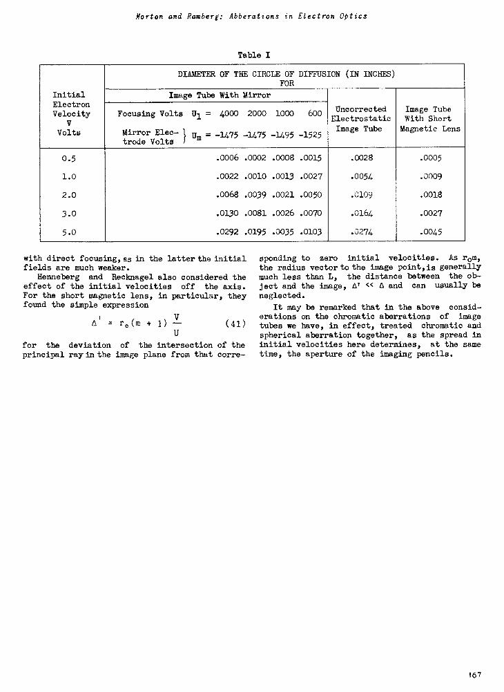
Norton and Ramberg: Abberations in Electron Optics
Table I
DIAMETER OF THE CIRCLE OF DIFFUSION (IN INCHES)FOR
Initial Image Tube With MirrorElectron
Uncorrected Image TubeVelocity
V
Focusing Volts U1 = 4000 2000 1000 600LI trostatic With Short
Volts Mirror Elec- 1 Um = -1475trode Volts
-1475 -1495 -1525Image Tube Magnetic Lens
0.5 .0006 .0002 .0008 .0015 .0028 .0005
1.0 .0022 .0010 .0013 .0027 .0054 .0009
2.0 .0068 .0039 .0021 .0050 .0109 .0018
3.0 .0130 .0081 .0026 .0070 .0164 .0027
5.0 .0292 .0195 .0035 .0103 .0274 .0045
with direct focusing, as in the latter the initialfields are much weaker.
Henneberg and Recknagel also considered theeffect of the initial velocities off the axis.For the short magnetic lens, in particular, theyfound the simple expression
A = ro(m + 1)V--
(41)U
for the deviation of the intersection of theprincipal ray in the image plane from that corre-
sponding to zero initial velocities. As rom,
the radius vector to the image point,is generallymuch less than L, the distance between the ob-
ject and the image, AI << A and can usually be
neglected.
It may be remarked that in the above consid-erations on the chromatic aberrations of imagetubes we have, in effect, treated chromatic andspherical aberration together, as the spread ininitial velocities here determines, at the sametime, the aperture of the imaging pencils.
167
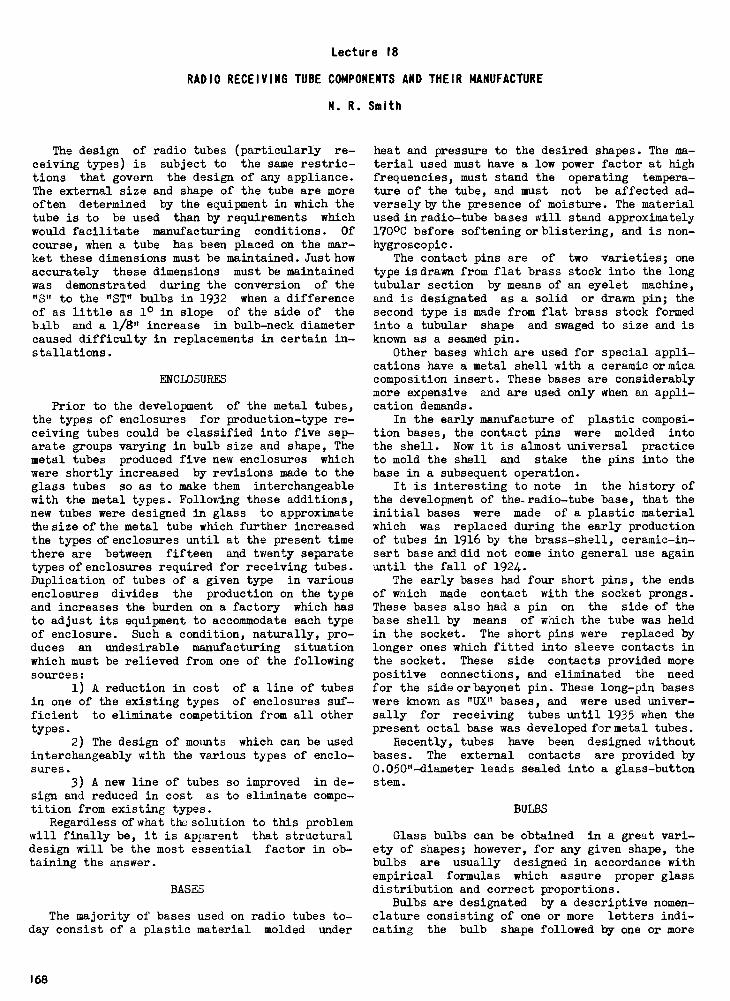
Lecture 18
RADIO RECEIVING TUBE COMPONENTS AND THEIR MANUFACTURE
N. R. Smith
The design of radio tubes (particularly re-ceiving types) is subject to the same restric-tions that govern the design of any appliance.The external size and shape of the tube are moreoften determined by the equipment in which thetube is to be used than by requirements whichwould facilitate manufacturing conditions. Ofcourse, when a tube has been placed on the mar-ket these dimensions must be maintained. Just howaccurately these dimensions must be maintainedwas demonstrated during the conversion of the"S" to the "ST" bulbs in 1932 when a differenceof as little as 1° in slope of the side of thebiLb and a 1/8" increase in bulb -neck diametercaused difficulty in replacements in certain in-stallations.
ENCLOSURES
Prior to the development of the metal tubes,the types of enclosures for production -type re-ceiving tubes could be classified into five sep-arate groups varying in bulb size and shape, Themetal tubes produced five new enclosures whichwere shortly increased by revisions made to theglass tubes so as to make them interchangeablewith the metal types. Following these additions,new tubes were designed in glass to approximatethe size of the metal tube which further increasedthe types of enclosures until at the present timethere are between fifteen and twenty separatetypes of enclosures required for receiving tubes.Duplication of tubes of a given type in variousenclosures divides the production on the typeand increases the burden on a factory which hasto adjust its equipment to accommodate each typeof enclosure. Such a condition, naturally, pro-duces an undesirable manufacturing situationwhich must be relieved from one of the followingsources:
1) A reduction in cost of a line of tubesin one of the existing types of enclosures suf-ficient to eliminate competition from all othertypes.
2) The design of mounts which can be usedinterchangeably with the various types of enclo-sures.
3) A new line of tubes so improved in de-sign and reduced in cost as to eliminate compe-tition from existing types.
Regardless of what the solution to this problemwill finally be, it is apparent that structuraldesign will be the most essential factor in ob-taining the answer.
BASES
The majority of bases used on radio tubes to-day consist of a plastic material molded under
heat and pressure to the desired shapes. The ma-terial used must have a low power factor at highfrequencies, must stand the operating tempera-ture of the tube, and must not be affected ad-verselyby the presence of moisture. The materialused in radio -tube bases will stand approximately1700C before softening or blistering, and is non -hygroscopic.
The contact pins are of two varieties; onetype is drawn from flat brass stock into the longtubular section by means of an eyelet machine,and is designated as a solid or drawn pin; thesecond type is made from flat brass stock formedinto a tubular shape and swaged to size and isknown as a seamed pin.
Other bases which are used for special appli-cations have a metal shell with a ceramic or micacomposition insert. These bases are considerablymore expensive and are used only when an appli-cation demands.
In the early manufacture of plastic composi-tion bases, the contact pins were molded intothe shell. Now it is almost universal practiceto mold the shell and stake the pins into thebase in a subsequent operation.
It is interesting to note in the history ofthe development of the -radio -tube base, that theinitial bases were made of a plastic materialwhich was replaced during the early productionof tubes in 1916 by the brass -shell, ceramic -in-sert base and did not come into general use againuntil the fall of 1924.
The early bases had four short pins, the endsof which made contact with the socket prongs.These bases also had a pin on the side of thebase shell by means of which the tube was heldin the socket. The short pins were replaced bylonger ones which fitted into sleeve contacts inthe socket. These side contacts provided morepositive connections, and eliminated the needfor the side or bayonet pin. These long -pin baseswere known as "UX" bases, and were used univer-sally for receiving tubes until 1935 when thepresent octal base was developed for metal tubes.
Recently, tubes have been designed withoutbases. The external contacts are provided by0.050" -diameter leads sealed into a glass -buttonstem.
BULBS
Glass bulbs can be obtained in a great vari-ety of shapes; however, for any given shape, thebulbs are usually designed in accordance withempirical formulas which assure proper glassdistribution and correct proportions.
Bulbs are designated by a descriptive nomen-clature consisting of one or more letters indi-cating the bulb shape followed by one or more
168
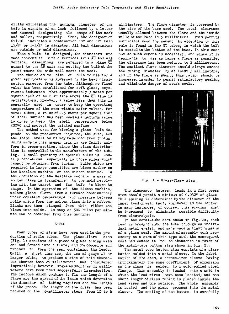
Smith: Radio Receiving Tube Components and Their Manufacture
digits expressing the maximum diameter of thebulb in eighths of an inch followed by a letterand numeral designating the shape of the neckand cullet, respectively. Thus, the designationST12D1 indicates a combination "S" and "T" bulb12/8" or 1-1/2" in diameter. All bulb dimensionsare outside or mold dimensions.
When a bulb is designed, the diameters aremade concentric with a vertical axis AB and allvertical dimensions are referred to a plane CDnormal to the AB axis and cutting the bulb at thepoint where the side wall meets the neck.
The choice as to size of bulb to use for agiven application is governed by the heat dissi-pation expected from the tube. Although no fixedvalue has been established for soft glass, expe-rience indicates that approximately 3 watts persquare inch of bulb surface above the CD line issatisfactory. However, a value less than this isgenerally used in order to keep the operatingtemperature of the stem within safer values. Formetal tubes, a value of 2.5 watts per square inchof shell surface has been used as a maximum valuein order to keep the shell temperature below2000C and protect the painted surface.
The method used for blowing a glass bulb de-pends on the production required, the size, andthe shape. Small bulbs may be molded from tubing.Bulbs made in this manner usually are fairly uni-form in cross-section, since the glass distribu-tion is controlled in the manufacture of the tub-ing. A small quantity of special bulbs is usu-ally hand -blown especially in those sizes whichcannot be obtained from tubing. Bulbs which arerequired in large quantities are blown either onthe Westlake machine or the Ribbon machine. In
the operation of the Westlake machine, a mass ofmolten glass is transferred to the mold revolv-ing with the turret and the bulb is blown toshape. In the operation of the Ribbon machine,molten glass flows from a furnace continuouslyunder constant temperature and pressure betweenrolls which form the molten glass into a ribbon.Blanks are then stamped from this ribbon andblown into molds. As many as 500 bulbs per min-ute can be obtained from this machine.
STEMS
Four types of stems have been used inthe pro-duction of radio tubes. The glass -flare stem(Fig. 1) consists of a piece of glass tubing withone end formed into a flare, and the opposite endpinched to form the seal containing the leads.Until a short time ago, the use of gauge 41 orlarger tubing to produce a stem of this charac-ter shorter than 29 millimeters was consideredimpractical; however, stems as short as 14 milli-meters have been used successfully in production.The factors which combine to fix the length of aflare are the spread of the leads which determinethe diameter of tubing required and the lengthof the press. The length of the press has beenreduced on the 14 -millimeter stems from 10 to 6
millimeters. The flare diameter is governed bythe size of the base used. The total clearanceusually allowed between the flare and the insidewalls of the base is 5 millimeters. This permitssufficient room for cement. An exception to thisrule is found in the GT tubes, in which the bulbis seated inthe bottom of the base. In this casenot so much cement is necessary, and since it isdesirable to use as large a flare as possible,the clearance has been reduced to 2 millimeters.The smallest flare diameter should always exceedthe tubing diameter by at least 3 millimeters,and if the flare is short, this ratio should beincreased in order to permit satisfactory sealingand eliminate danger of stuck seals.
Fig. 1 - Glass -flare stem.
The clearance between leads in a flat -pressstem should permit a minimum of 0.030" of glass.This spacing is determined by the diameter of theinner lead or weld knot, whichever is the larger.In many instances, of course, this spacing mustbe increased to eliminate possible difficultyfrom electrolysis.
In the metal -tube stem shown in Fig. 2a, eachlead is brought into the tube through an indivi-dual metal eyelet, and made vacuum tight by meansof a glass seal. The amount of assembly work nec-essary on a stem of this type with the consequentcost has caused it to be abandoned in favor ofthe metal -tube button stem shown in Fig. 2b.
The metal -tube button stem consists of a glassbutton molded into a metal sleeve. In the fabri-cation of the stem, a chrome -iron sleeve havingapproximately the same coefficient of expansionas the glass is welded to a cold -rolled steelflange. This assembly is loaded onto a mold inwhich the lead wires have been located; and oneshort length of glass tubing is placed inside thelead wires and one outside. The whole assemblyis heated and the glass pressed into the metalsleeve. The cooling of the button is carefully
169
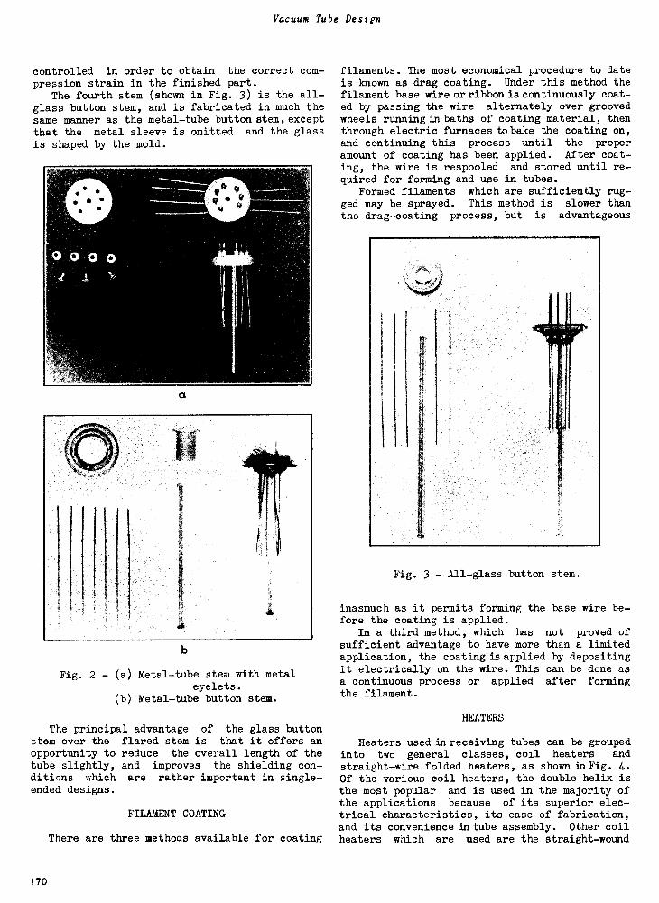
Vacuum Tube Design
controlled in order to obtain the correct com-pression strain in the finished part.
The fourth stem (shown in Fig. 3) is the all -glass button stem, and is fabricated in much thesame manner as the metal -tube button stem, except
that the metal sleeve is omitted and the glassis shaped by the mold.
*
0 09 4
a
b
Fig. 2 - (a) Metal -tube stem with metaleyelets.
(b) Metal -tube button stem.
The principal advantage of the glass buttonstem over the flared stem is that it offers anopportunity to reduce the overall length of thetube slightly, and improves the shielding con-ditions which are rather important in single -ended designs.
FILAMENT COATING
There are three methods available for coating
filaments. The most economical procedure to dateis known as drag coating. Under this method thefilament base wire or ribbon is continuously coat-ed by passing the wire alternately over groovedwheels running in baths of coating material, thenthrough electric furnaces to bake the coating on,and continuing this process until the proper
amount of coating has been applied. After coat-ing, the wire is respooled and stored until re-quired for forming and use in tubes.
Formed filaments which are sufficiently rug-ged may be sprayed. This method is slower thanthe drag -coating process, but is advantageous
Fig. 3 - All -glass button stem.
inasmuch as it permits forming the base wire be-fore the coating is applied.
In a third method, which has not proved ofsufficient advantage to have more than a limitedapplication, the coating is applied by depositingit electrically on the wire. This can be done asa continuous process or applied after formingthe filament.
HEATERS
Heaters used in receiving tubes can be groupedinto two general classes, coil heaters andstraight -wire folded heaters, as shown in Fig. 4.Of the various coil heaters, the double helix isthe most popular and is used in the majority ofthe applications because of its superior elec-trical characteristics, its ease of fabrication,and its convenience in tube assembly. Other coilheaters which are used are the straight -wound
170
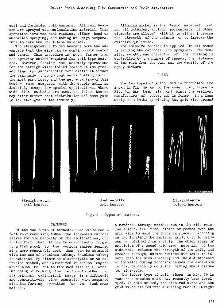
Smith: Radio Receiving Tube Components and Their Manufacture
coil and the folded coil heaters. All coil heat-ers are sprayed with an insulating material. Thisoperation involves hand -racking, either hand orautomatic spraying, and baking at high tempera-ture to cure the insulation material.
The straight -wire folded heaters have the ad-vantage that the wire can be continuously coatedand baked. This procedure is much faster thanthe spraying method required for coil -type heat-ers. However, forming and assembly operationsfor the straight -wire folded heater at the pres-ent time, are sufficiently more difficult so thatthe gain made through continuous coating is forthe most part lost, and the net advantage of thisheater when compared with the double helix isdoubtful, except for special applications. Wherewide flat cathodes are used, the folded heatermay offer better heat distribution and some gainin the strength of the assembly.
Straight -wound
coil heaters
Although nickel is the basic material usedfor all cathodes, various percentages of otherelements are alloyed with it to either increasethe strength of the cathode or to improve theemissive qualities.
The emissive coating is applied in all casesby racking the cathodes and spraying. The den-sity, weight, and character of the coating iscontrolled by the number of passes, the distanceof the rack from the gun, and the density of thespray mixture.
GRIDS
The two types of grids used in production areshown in Fig. 5a and b. The wound grid, shown inFig. 5a, has been standard since the earliestmanufacture of tubes, and is formed in a longstrip on a lathe by winding the grid wire around
Double -helix
coil heaters
Fig. 4 - Types of heaters.
CATHODES
Of the two forms of cathodes used in the manu-facture of receiving tubes, the lock -seam cathodeserves for the majority of the applications, dueto the fact that it can be conveniently formedfrom flat stock to the various shapes desiredat a more reasonable cost than can be obtainedwith the use of seamless tubing. Seamless tubingis obtained by either an electrolytic or an ex-trusion method, and is received in random lengthswhich must be cut to finished size in a lathe.Embossing or forming the cathode to other thanits original cylindrical shape is a difficultand comparatively slow operation when comparedwith the forming operation for the lock -seamcathode.
Straight -wire
folded heaters
a mandrel through notches cut in the side -rods.The notches are then closed or peened over thegrid wire to hold the turns in place. Dependingon the length of the finished grid, 6 to 10 gridscan be obtained from a strip. The chief items ofcriticism of a wound grid are: notching of the
side -rods reduces the strength of the grid, andcreates a rough, uneven surface difficult to in-sert into the mica spacers; and the displacementof the metal during notching causes the side -rodsto bow, especially on grids having small diame-ter side -rods.
The ladder type of grid shown in Fig. 5b ismade on a machine which has recently been devel-oped. In this method, the side -rod wires and thegrid wires are fed into a welding machine at right
171
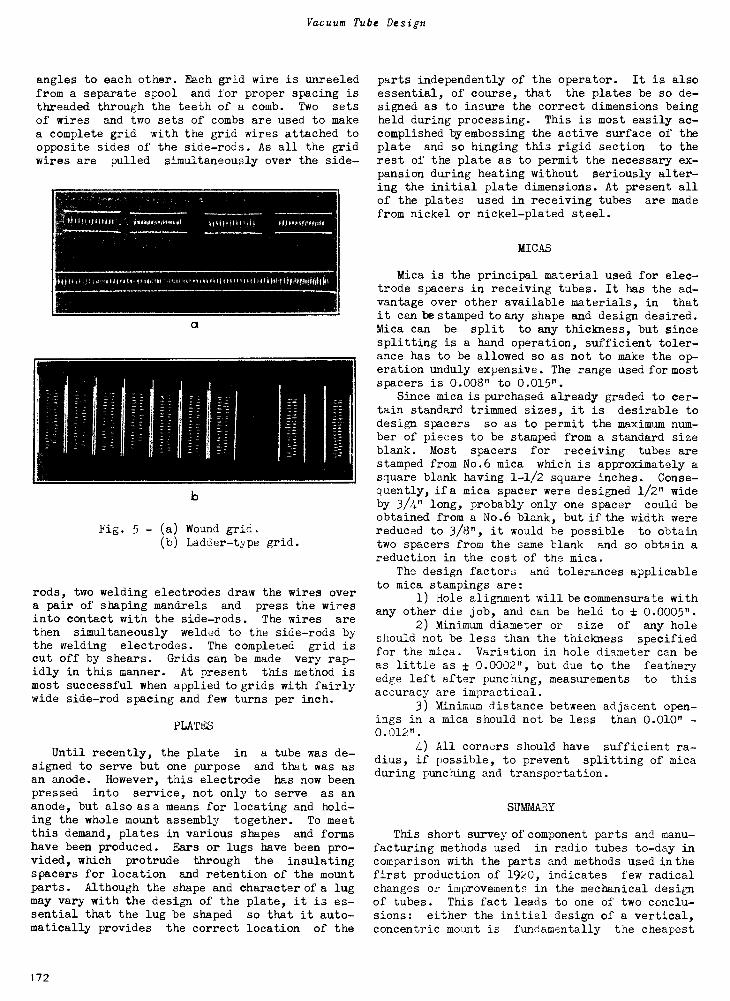
Vacuum Tube Design
angles to each other. Each grid wire is unreeledfrom a separate spool and for proper spacing isthreaded through the teeth of a comb. Two setsof wires and two sets of combs are used to makea complete grid with the grid wires attached toopposite sides of the side -rods. As all the gridwires are pulled simultaneously over the side -
a
b
Fig. 5 - (a) Wound grid.(b) Ladder -type grid.
rods, two weldinga pair of shapinginto contact with
electrodes draw the wires overmandrels and press the wiresthe side -rods. The wires are
then simultaneously welded to the side -rods bythe welding electrodes. The completed grid iscut off by shears. Grids can be made very rap-idly in this manner. At present this method ismost successful when applied to grids with fairlywide side -rod spacing and few turns per inch.
PLATES
Until recently, the plate in a tube was de-signed to serve but one purpose and that was asan anode. However, this electrode has now beenpressed into service, not only to serve as ananode, but also asa means for locating and hold-ing the whole mount assembly together. To meetthis demand, plates in various shapes and formshave been produced. Ears or lugs have been pro-vided, which protrude through the insulatingspacers for location and retention of the mountparts. Although the shape and character of a lugmay vary with the design of the plate, it is es-sential that the lug be shaped so that it auto-matically provides the correct location of the
parts independently of the operator. It is alsoessential, of course, that the plates be so de-signed as to insure the correct dimensions beingheld during processing. This is most easily ac-complished by embossing the active surface of theplate and so hinging this rigid section to therest of the plate as to permit the necessary ex-pansion during heating without seriously alter-ing the initial plate dimensions. At present allof the plates used in receiving tubes are madefrom nickel or nickel -plated steel.
MICAS
Mica is the principal material used for elec-trode spacers in receiving tubes. It has the ad-vantage over other available materials, in thatit can be stamped to any shape and design desired.Mica can be split to any thickness, but sincesplitting is a hand operation, sufficient toler-ance has to be allowed so as not to make the op-eration unduly expensive. The range used for mostspacers is 0.008" to 0.015".
Since mica is purchased already graded to cer-tain standard trimmed sizes, it is desirable todesign spacers so as to permit the maximum num-ber of pieces to be stamped from a standard sizeblank. Most spacers for receiving tubes arestamped from No.6 mica which is approximately asquare blank having 1-1/2 square inches. Conse-quently, if a mica spacer were designed 1/2" wideby 3/4" long, probably only one spacer could beobtained from a No.6 blank, but if the width werereduced to 3/8", it would be possible to obtaintwo spacers from the same blank and so obtain areduction in the cost of the mica.
The design factors and tolerances applicableto mica stampings are:
1) Hole alignment will be commensurate withany other die job, and can be held to ± 0.0005".
2) Minimum diameter or size of any holeshould not be less than the thickness specifiedfor the mica. Variation in hole diameter can beas little as ± 0.0002", but due to the featheryedge left after punching, measurements to thisaccuracy are impractical.
3) Minimum distance between adjacent open-ings in a mica should not be less than 0.010" -0.012".
4) All corners should have sufficient ra-dius, if possible, to prevent splitting of micaduring punching and transportation.
SUMMARY
This short survey of component parts and manu-facturing methods used in radio tubes to -day incomparison with the parts and methods used in thefirst production of 1920, indicates few radicalchanges or improvements in the mechanical designof tubes. This fact leads to one of two conclu-sions: either the initial design of a vertical,concentric mount is fundamentally the cheapest
172

Smith: Radio Receiving Tube Components and Their Manufacture
and best design which can be conceived, or thepossibilities to be derived from mechanical de-sign have not been thoroughly investigated.
Recently, considerable effort has been di-rected by all manufacturers toward the improve-ment, reduction in size, and reduction in costof the vertical, concentric mount. Much can beaccomplished in this direction; however, the re-sults of this effort have in many instances only
served to complicate the manufacturing problemswithout attaining real advantages.
Consequently, I believe it is a safe predic-tion to say that the ultimate answer to the de-mand for smaller, lower -priced tubes will not befound in improvements which can be made on thevertical -concentric mount, but will be the re-sult of an entirely new structural design adapt-able to more economical manufacturing methods.
173
Lecture 19
ANALYSIS OF RECTIFIER OPERATION
0. H. Schade
INTRODUCTION
The design of diodes for rectification of a -cpower requires unusual care even though theirdesign is simple from the standpoint of the num-ber of electrodes involved. The cathode must becapable of supplying the average current andpeak current which will be encountered in ser-vice. The plate must operate at a safe temper-ature, which in turn depends on plate dissipa-tion, the physical dimensions of the plate, andthe thermionic and thermal emissivity of theplate material. Another factor to be consideredis the perveance of the diode, i.e., the steep-ness of its voltage -current characteristic. Per-veance affects both cathode- and plate -designbecause it controls current density and voltagegradient at the effective surfaces of both for agiven cathode area. Then, too, there is the re-quirement for adequate insulation. Perveanceand insulation requirements depend on the typeof service in which the diode is to be used.
It is apparent that an analysis of diode -operating conditions in rectifier circuits is
essential in order to arrive at optimum designspecifications in each particular case, becausethe required data bear no simple relationship tothe values of rectified current and voltage.
PRINCIPLES OF RECTIFICATION
1. General
Rectification is a process of synchronizedswitching. The basic rectifier circuit consistsof one synchronized switch in series with asingle-phase source of single frequency and a
resistance load. The switch connection betweenload terminals and source is closed when sourceand load terminals have the same polarity, andis open during the time of opposite polarity.The load current consists of half -wave pulses.This simple circuit is unsuitable for most prac-tical purposes, because it does not furnish asmooth load current.
The current may be smoothed by two methods:(a) by increasing the number of phases, and (b)by inserting reactive elements into the circuit.The phase number is limited to two for radio re-ceivers. The circuit analysis which followslateralwill treat single- and double -phase rec-tifier circuits with reactive circuit elements.
Switching in reactive circuits gives rise to"transients." Current and voltage can, there-fore, not be computed according to steady-statemethods.
The diode functions as a self -timing elec-tronic switch. It closes the circuit when theplate becomes positive with respect to cathode
and opens the circuit at the instant when theplate current becomes zero.
The diode has an internal resistance whichis a function of current. When analyzing recti-fier circuits, it is convenient to treat the in-ternal resistance of the diode rectifier as anelement, separated from the "switch action" ofthe diode. Fig. 1 illustrates the three circuitelements so obtained. The diode characteristicis the geometric sum of these characteristics.The resistance rd is effective only when theswitch is closed, i.e., during the conductionperiod of the diode. The effective diode re-sistance must, therefore, be measured or evalu-
Id= Ip1
rE0-1
0 0-E 0 4:17fp
I EXTERNALLYI APPLIEDI VOLTAGE
SYNCHRO-NIZED
SW ITCH
71111-
0- +Ed --..-/DilODEVOLTAGE
Ec,ra
-NMM/- 41141F1111-WV"---
INTER- NON -+ NAL + LINEAR = EQUIVALENT CIRCUIT
POTENTIAL RESISTANCE
Fig. 1
ated within conduction -time limits. Consider aswitch in series with a fixed resistance and anynumber of other circuit elements connected to abattery of fixed voltage. The d -c current andrms current which flow in this circuit will de-pend on the time intervals during which theswitch is closed and open; the resistance valueis not obtainable from these current values andthe battery voltage. The correct value is ob-tained only when the current and voltage drop inthe resistance are measured during the time anglep (Fig. 2) when the switch is closed.
The method of analysis of rectifier circuitsto be discussed in this lecture is based on theprinciple that the non-linear effective resist-ance of the diode may be replaced analyticallyby an equivalent fixed resistance which willgive a diode current equal to that obtained withthe actual non-linear diode resistance. The cor-rect value to be used for the equivalent fixedresistance depends upon whether we are analyzingfor peak diode current, average diode current,or rms diode current. As will be seen later, therelations among these three equivalent resist -
174
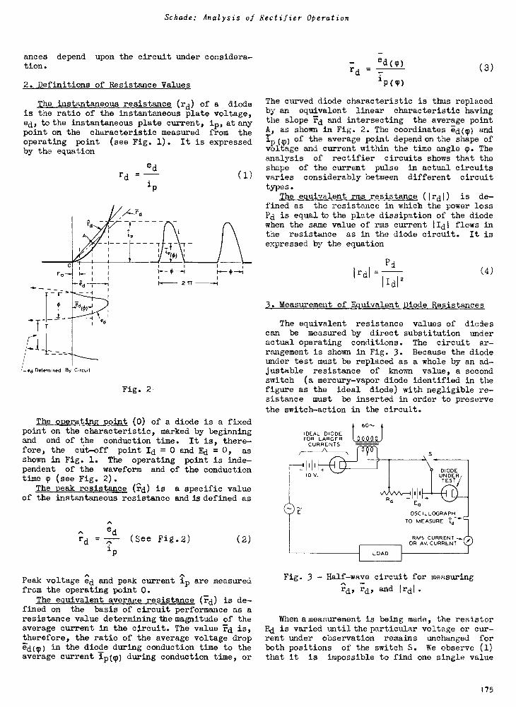
Schade: Analysis of Rectifier Operation
ances depend upon the circuit under considera-tion.
2. Definitions of Resistance Values
The instantaneous resistance (rd) of a diodeis the ratio of the instantaneous plate voltage,ed, to the instantaneous plate current, ip, at anypoint on the characteristic measured from theoperating point (see Fig. 1). It is expressedby the equation
rd
i-ed Determined By Circuit
edrd = -
ip
rd
Ip
Fig. 2
I.-2 TT
(1)
The operating point (0) of a diode is a fixedpoint on the characteristic, marked by beginningand end of the conduction time. It is, there-fore, the cut-off point Id = 0 and Ed = 0, asshown in Fig. 1. The operating point is inde-pendent of the waveform and of the conductiontime T (see Fig. 2).
The peak resistance (rd) is a specific valueof the instantaneous resistance and is defined as
rded
(See Fig.2)ip
(2)
Peak voltage ed and peak current ip are measuredfrom the operating point 0.
The equivalent average resistance (rd) is de-fined on the basis of circuit performance as aresistance value determining the magnitude of theaverage current in the circuit. The value rd is,therefore, the ratio of the average voltage dropId(v in the diode during conduction time to theaverage current ipoo during conduction time, or
-edop)
rd -
1P(T)
(2)
The curved diode characteristic is thus replacedby an equivalent linear characteristic havingthe slope rd and intersecting the average pointA, as shown in Fig. 2. The coordinates id(T) andip(p) of the average point depend on the shape ofvoltage and current within the time angle T. Theanalysis of rectifier circuits shows that theshape of the current pulse in actual circuitsvaries considerably between different circuittypes.
The equivalent rms resistance (Irdi) is de-fined as the resistance in which the power lossPd is equal to the plate dissipation of the diodewhen the same value of rms current lid' flows inthe resistance as in the diode circuit. It isexpressed by the equation
Pd
Irdl(4)
3. Measurement of Equivalent Diode Resistances
The equivalent resistance values of diodescan be measured by direct substitution underactual operating conditions. The circuit ar-rangement is shown in Fig. 3. Because the diodeunder test must be replaced as a whole by an ad-justable resistance of known value, a secondswitch (a mercury-vapor diode identified in thefigure as the ideal diode) with negligible re-sistance must be inserted in order to preservethe switch -action in the circuit.
IDEAL DIODEFOR LARGER
CURRENTS
ata 111.
111.710 V.
+E0
OSC I L LOGRAP H
TO MEASURE ld
RMS CURRENTOR AV. CURRENT
Fig. 3 - Half -wave circuit for measuring
rd, rd, and Irdl.
When ameasurement is being made, the resistorRd is varied until the particular voltage or cur-rent under observation remains unchanged forboth positions of the switch S. We observe (1)that it is impossible to find one single value
175
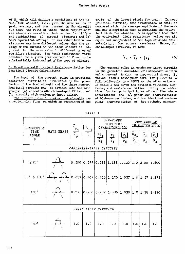
Vacuum Tube Design
of Rd which will duplicate conditions of the ac-tual tube circuit, i.e., give the same values ofpeak, average, and rms current in the circuit;(2) that the ratio of these three "equivalent"resistance values of the diode varies for differ-ent combinations of circuit elements; and (3)that equivalent average or rms substitution re-sistances may have different values when the av-erage or rms current in the diode circuit is ad-justed to the same value in different types ofrectifier circuits. The "peak resistance" valueobtained for a given peak current is found to besubstantially independent of the type of circuit.
4. Waveforms and Equivalent Resistance Ratios forPractical Circuit Calculations
The form of the current pulse in practicalrectifier circuits is determined by the powerfactor of the load circuit and the phase number.Practical circuits may be divided into two maingroups: (a) circuits with choke -input filter; and(b) circuits with condenser -input filter.
The current pulse in choke -input circuits hasa rectangular form on which is superimposed one
cycle of the lowest ripple frequency. In mostpractical circuits, this fluctuation is small ascompared with the average amplitude of the waveand maybe neglected when determining the equiva-lent diode resistances. It is apparent then thatthe equivalent diode resistance values are allequal and independent of the type of diode char-acteristics for square waveforms. Hence, forchoke -input circuits, we have
rd = rd = 'red(5)
The current pulse in condenser -input circuitsis the geometric summation of a sine -wave sectionand a current having an exponential decay. Itvaries from a triangular form for p < 200 to a
full half -cycle (p = 180°) as the other extreme.In Table I are given the ratios of voltages, cur-rents, and resistance values during conductiontime for two principal types of rectifier char-acteristics: the 3/2 -power -law characteristicof high -vacuum diodes, and the idealized rectan-gular characteristic of hot -cathode, mercury -
Table I
CONDUCTIONTIMEANGLE
T
WAVE SHAPE
ip 1 ipl
3/2 -POWER
RECTIFIERCHARACTERISTIC
RECTANGULARCHARACTERISTIC
--
rd Irdl edcp rdAArd
I rdl
772iP
--PA
ed^rd
AArd ed rd
CONDENSER -INPUT CIRCUITS
..4 20°
90° & 180°
1300
0.500
0.637
0.725
0.577
0.707
0.780
0.593
0.715
0.787
1.185
1.120
1.085
1.120
1.057
1.030
1.0
1.0
1.0
2.00
1.57
1.38
1.500
1.272
1.190
-,Lik-; ,
J
-1--[\-i \
CHOKE -INPUT CIRCUITS
180° 1.0 1.0 1.0 1.0 1.0 1.0 1.0 1.0.
, \
176
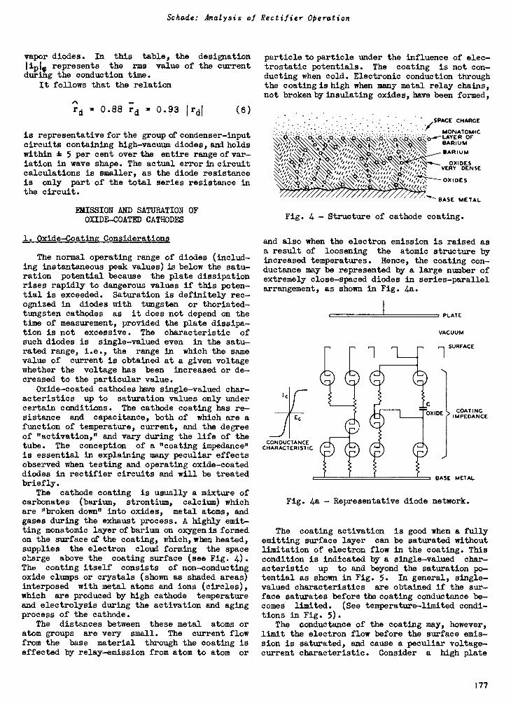
Schade: Analysis of Rectifier Operation
vapor diodes. In this table, the designationIipIq represents the rms value of the currentduring the conduction time.
It follows that the relation
rd = 0.88 rd = 0.93I rdl (6)
is representative for the group of condenser -inputcircuits containing high -vacuum diodes, and holdswithin * 5 per cent over the entire range of var-iation in wave shape. The actual error in circuitcalculations is smaller, as the diode resistanceis only part of the total series resistance inthe circuit.
EMISSION AND SATURATION OFOXIDE -COATED CATHODES
1. Oxide -Coating Considerations
The normal operating range of diodes (includ-ing instantaneous peak values) is below the satu-ration potential because the plate dissipationrises rapidly to dangerous values if this poten-tial is exceeded. Saturation is definitely rec-ognized in diodes with tungsten or thoriated -tungsten cathodes as it does not depend on thetime of measurement, provided the plate dissipa-tion is not excessive. The characteristic ofsuch diodes is single -valued even in the satu-rated range, i.e., the range in which the samevalue of current is obtained at a given voltagewhether the voltage has been increased or de-creased to the particular value.
Oxide -coated cathodes have single -valued char-acteristics up to saturation values only undercertain conditions. The cathode coating has re-sistance and capacitance, both of which are afunction of temperature, current, and the degreeof "activation," and vary during the life of thetube. The conception of a "coating impedance"is essential in explaining many peculiar effectsobserved when testing and operating oxide -coateddiodes in rectifier circuits and will be treatedbriefly.
The cathode coating is usually a mixture ofcarbonates (barium, strontium, calcium) whichare "broken down" into oxides, metal atoms, andgases during the exhaust process. A highly emit-ting monatomic layer of barium on oxygen is formedon the surface of the coating, which, when heated,supplies the electron cloud forming the spacecharge above the coating surface (see Fig. 4).The coating itself consists of non -conductingoxide clumps or crystals (shown as shaded areas)interposed with metal atoms and ions (circles),which are produced by high cathode temperatureand electrolysis during the activation and agingprocess of the cathode.
The distances between these metal atoms oratom groups are very small. The current flowfrom the base material through the coating iseffected by relay -emission from atom to atom or
particle to particle under the influence of elec-trostatic potentials. The coating is not con-ducting when cold. Electronic conduction throughthe coating is high when many metal relay chains,not broken by insulating oxides, have been formed,
//I, ON:
SPACE CHARGE
MONATOMIC
\O BARIUM
\ BARIUM
OXVERYIDES
." OXIDES
DENSE
BASE METAL
Fig. 4 - Structure of cathode coating.
and also when the electron emission is raised asa result of loosening the atomic structure byincreased temperatures. Hence, the coating con-ductance may be represented by a large number ofextremely close -spaced diodes in series -parallelarrangement, as shown in Fig. 4a.
CONDUCTANCECHARACTERISTIC
PLATE
VACUUM
1SURFACE
C
OXIDE COATINGIMPEDANCE
BASE METAL
Fig. 4a - Representative diode network.
The coating activationemitting surface layer canlimitation of electron flowcondition is indicated by a
is good when a fullybe saturated withoutin the coating. Thissingle -valued char-
acteristic up to and beyond the saturation po-tential as shown in Fig. 5. In general, single -valued characteristics are obtained if the sur-face saturates before the coating conductance be-comes limited. (See temperature -limited condi-tions in Fig. 5).
The conductance of the coating may, however,limit the electron flow before the surface emis-sion is saturated, and cause a peculiar voltage -current characteristic. Consider a high plate
177
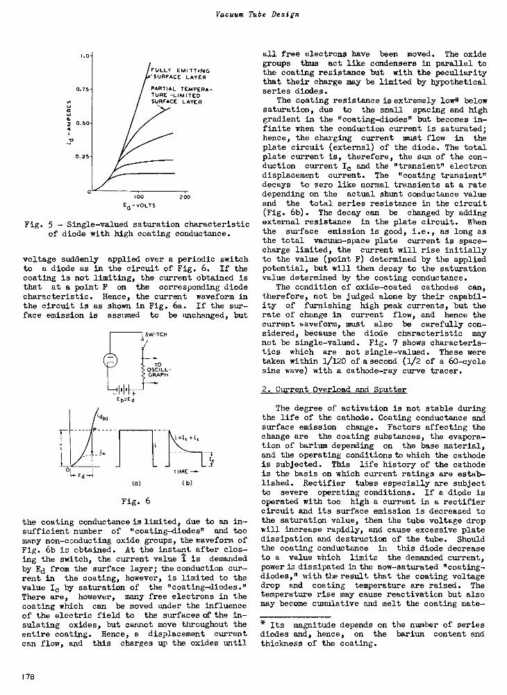
Vacuum Tube Design
1.0
0.75
IIa.
0.504
0.25
FULLY EMITTINGSURFACE LAYER
PARTIAL TEMPERA-TURE -LIMITEDSURFACE LAYER
100
Ed -VOLTS200
Fig. 5 - Single -valued saturation characteristicof diode with high coating conductance.
voltage suddenly applied over a periodic switchto a diode as in the circuit of Fig. 6. If thecoating is not limiting, the current obtained isthat at a point P on the corresponding diodecharacteristic. Hence, the current waveform inthe circuit is as shown in Fig. 6a. If the sur-face emission is assumed to be unchanged, but
SWITCH
TOOSCILL-GRAPH
EbrEd
TIME -0-
(a) (b)
Fig. 6
the coating conductance is limited, due to an in-sufficient number of "coating -diodes" and toomany non -conducting oxide groups, the waveform ofFig. 6b is obtained. At the instant after clos-ing the switch, the current value i is demanded
by Ed from the surface layer; the conduction cur-rent in the coating, however, is limited to thevalue Ic by saturation of the "coating -diodes."
There are, however, many free electrons in thecoating which can be moved under the influenceof the electric field to the surfaces of the in-
sulating oxides, but cannot move throughout theentire coating. Hence, a displacement currentcan flow, and this charges up the oxides until
all free electrons have been moved. The oxidegroups thus act like condensers in parallel tothe coating resistance but with the peculiaritythat their charge may be limited by hypotheticalseries diodes.
The coating resistance is extremely low* belowsaturation, due to the small spacing and highgradient in the "coating -diodes" but becomes in-finite when the conduction current is saturated;hence, the charging current must flow in theplate circuit (external) of the diode. The totalplate current is, therefore, the sum of the con-duction current Ic and the "transient" electrondisplacement current. The "coating transient"decays to zero like normal transients at a ratedepending on the actual shunt conductance valueand the total series resistance in the circuit(Fig. 6b). The decay can be changed by addingexternal resistance in the plate circuit. Whenthe surface emission is good, i.e., as long asthe total vacuum -space plate current is space -charge limited, the current will rise initiallyto the value (point P) determined by the appliedpotential, but will then decay to the saturationvalue determined by the coating conductance.
The condition of oxide -coated cathodes can,
therefore, not be judged alone by their capabil-ity of furnishing high peak currents, but therate of change in current flow, and hence thecurrent waveform, must also be carefully con-sidered, because the diode characteristic maynot be single -valued. Fig. 7 shows characteris-tics which are not single -valued. These weretaken within 1/120 of a second (1/2 of a 60 -cyclesine wave) with a cathode-ray curve tracer.
2. Current Overload and Sputter
The degree of activation is not stable duringthe life of the cathode. Coating conductance andsurface emission change. Factors affecting thechange are the coating substances, the evapora-tion of barium depending on the base material,and the operating conditions to which the cathodeis subjected. This life history of the cathodeis the basis on which current ratings are estab-lished. Rectifier tubes especially are subjectto severe operating conditions. If a diode isoperated with too high a current in a rectifiercircuit and its surface emission is decreased tothe saturation value, then the tube voltage dropwill increase rapidly, and cause excessive platedissipation and destruction of the tube. Shouldthe coating conductance in this diode decreaseto a value which limits the demanded current,power is dissipated in the now -saturated "coating -diodes," with the result that the coating voltagedrop and coating temperature are raised. Thetemperature rise may cause reactivation but alsomay become cumulative and melt the coating mate-
* Its magnitude depends on the number of seriesdiodes and, hence, on the barium content andthickness of the coating.
178
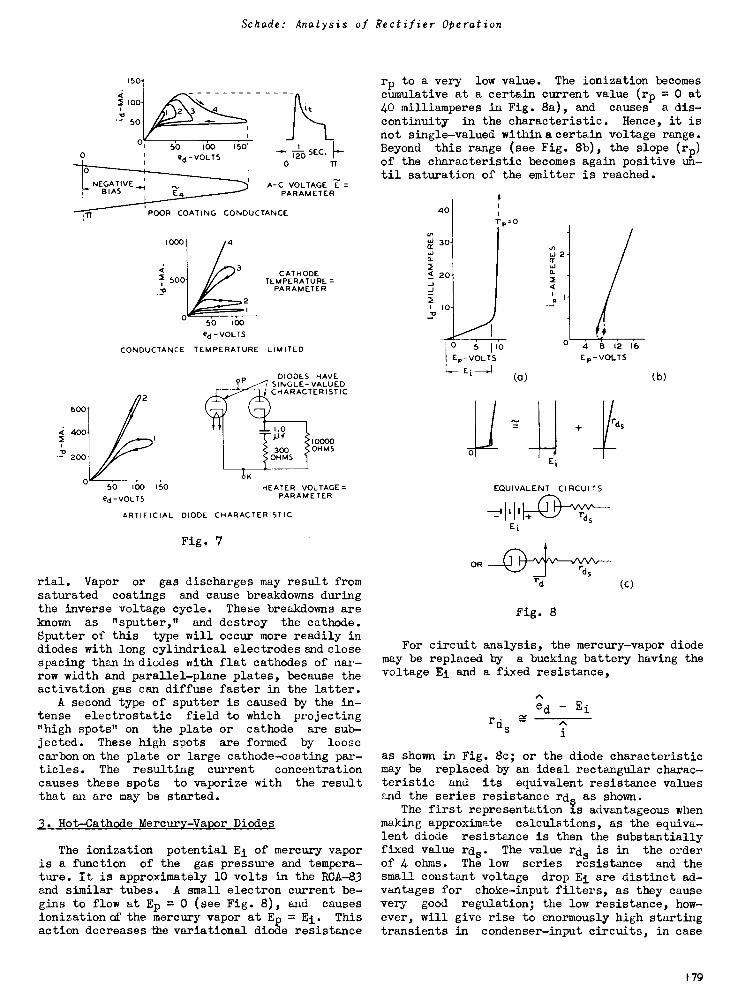
Schade: Analysis of Rectifier Operation
ed-VOLTS
0
NEGATIVEBIAS E4
A -C VOLTAGE E =PARAMETER
TT POOR COATING CONDUCTANCE
CAT HODETEMPERATURE=
PARAMETER
50 100
ed -VOLTS
CONDUCTANCE TEMPERATURE LIMITED
DIODES HAVESINGLE -VALUEDCHARACTERISTIC
10000OHMS
50 100 ISO HEATER VOLTAGE=PARAMETER
ARTIFICIAL DIODE CHARACTERISTIC
Fig. 7
rial. Vapor or gas discharges may result fromsaturated coatings and cause breakdowns duringthe inverse voltage cycle. These breakdowns areknown as "sputter," and destroy the cathode.Sputter of this type will occur more readily indiodes with long cylindrical electrodes and closespacing than in diodes with flat cathodes of nar-row width and parallel -plane plates, because theactivation gas can diffuse faster in the latter.
A second type of sputter is caused by the in-tense electrostatic field to which projecting"high spots" on the plate or cathode are sub-jected. These high spots are formed by loosecarbon on the plate or large cathode -coating par-ticles. The resulting current concentrationcauses these spots to vaporize with the resultthat an arc may be started.
3. Hot -Cathode Mercury -Vapor Diodes
The ionization potential Ei of mercury vaporis a function of the gas pressure and tempera-ture. It is approximately 10 volts in the RCA -83and similar tubes. A small electron current be-gins to flow at Ep = 0 (see Fig. 8), and causesionization off the mercury vapor at E = Ei. Thisaction decreases the variational diode resistance
rp to a very low value. The ionization becomescumulative at a certain current value (rp = 0 at40 milliamperes in Fig. 8a), and causes a dis-continuity in the characteristic. Hence, it isnot single -valued within a certain voltage range.Beyond this range (see Fig. 8b), the slope (rp)of the characteristic becomes again positive un-til saturation of the emitter is reached.
40T
,,,td 30
2< 20-J_J
10
=0
0 5 HO
Ep- VOLT S
- EL ---.-I
(0)
0
OR
Li 2cr
a -
a
0
Ei
EP -VOLTS
EQUIVALENT CIRCUITS
rd
Fig. 8
d s
rds
(C)
(b)
For circuit analysis, the mercury-vapor diodemay be replaced by a bucking battery having thevoltage Ei and a fixed resistance,
rdsed - Ei
as shown in Fig. 8c; or the diode characteristicmay be replaced by an ideal rectangular charac-teristic and its equivalent resistance valuesand the series resistance rds as shown.
The first representation is advantageous whenmaking approximate calculations, as the equiva-lent diode resistance is then the substantiallyfixed value rds. The value rds is in the orderof 4 ohms. The low series resistance and thesmall constant voltage drop Ei are distinct ad-vantages for choke -input filters, as they causevery good regulation; the low resistance, how-ever, will give rise to enormously high startingtransients in condenser -input circuits, in case
179
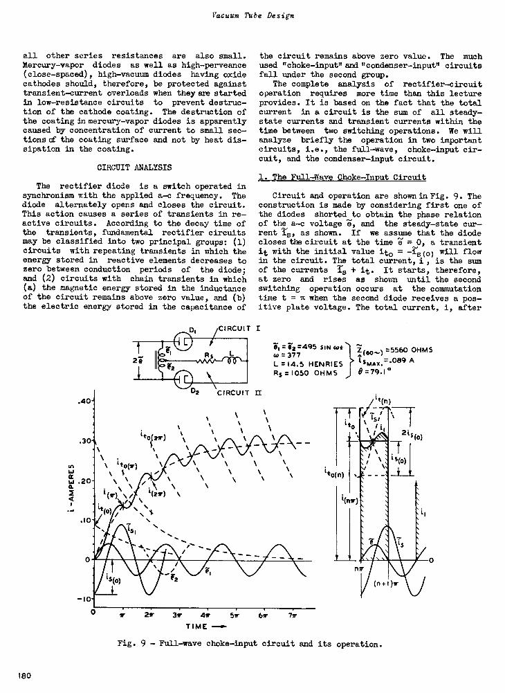
Vacuum Tube Design
all other series resistances are also small.Mercury-vapor diodes as well as high-perveance(close-spaced), high-vacuum diodes having oxidecathodes should, therefore, be protected againsttransient-current overloads when they are startedin low-resistance circuits to prevent destruc-tion of the cathode coating. The destruction ofthe coating in mercury-vapor diodes is apparentlycaused by concentration of current to small sec -tionscf the coating surface and not by heat dis-sipation in the coating.
CIRCUIT ANALYSIS
The rectifier diode is a switch operated insynchronism with the applied a-c frequency. Thediode alternately opens and closes the circuit.This action causes a series of transients in re-active circuits. According to the decay time ofthe transients, fundamental rectifier circuitsmay be classified into two principal groups: (1)circuits with repeating transients in which theenergy stored in reactive elements decreases tozero between conduction periods of the diode;and (2) circuits with chain transients in which(a) the magnetic energy stored in the inductanceof the circuit remains above zero value, and (b)the electric energy stored in the capacitance of
.40-
.301 \
\ .
0 tto(7)
$
w .20-a.2
k(o).10-
-10-0
ito(zw)
t(27r)
F2
the circuit remains above zero value. The muchused "choke -input"amd "condenser-input" circuitsfall under the second group.
The complete analysis of rectifier-circuitoperation requires more time than this lectureprovides. It is based on the fact that the totalcurrent in a circuit is the sum of all steady-state currents and transient currents within thetime between two switching operations. We willanalyze briefly the operation in two importantcircuits, i.e., the full-wave, choke-input cir-cuit, and the condenser-input circuit.
1. The Full-Wave Choke-Input Circuit
Circuit and operation are shown in Fig. 9. Theconstruction is made by considering first one ofthe diodes shorted to obtain the phase relationof the a-c voltage '4, and the steady-state cur-rent is, as shown. If we assume that the diodecloses the circuit at the time e = 0, a transientit with the initial value ito = -ism will flowin the circuit. The total current, i, is the sumof the currents is + it. It starts, therefore,at zero and rises as shorn until the secondswitching operation occurs at the commutationtime t = it when the second diode receives a pos-itive plate voltage. The total current, i, after
To, = e2 =495 SIN cut
co = 377L =14.5 HENRIESRs =1050 OHMS
w 2r 3w 4w 57r
TIME "..."
6w 77r
i*o n)
i(60,,) =5560 OHMS
ismAx.=°89 A6=79.1°
i(nir)
nv
j(o)
n+ v
Fig. 9 - Full-wave choke-input circuit and its operation.
180
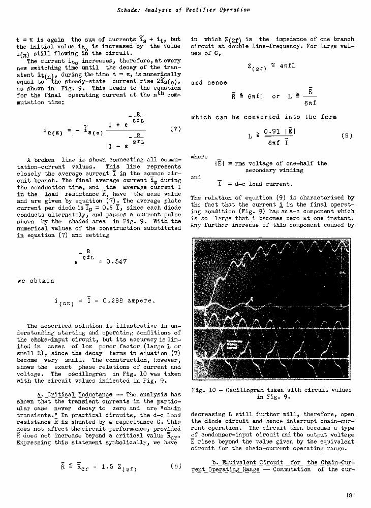
Schade: Analysis of Rectifier Operation
t = n is again the sum of currents Is + it, butthe initial value ito is increased by the value
i(n) still flowing in the circuit.The current ito increases, therefore, at every
new switching time until the decay of the tran-sient it(n), during the time t = it, is numerically
equal to the steady-state current rise 2is(0),
as shown in Fig. 9. This leads to the equation
for the final operating current at the nth com-
mutation time:
Inn) = -(n) s(0)
R
2EL1 + E
Raft,
1 - e
(7)
A broken line is shown connecting all commu-tation -current values. This line representsclosely the average current I in the common cir-cuit branch. The final average current i(1) duringthe conduction time, and _the average current Iin the load resistance R, have the same valueand are given by equation (7). The average platecurrent per diode is 1p = 0.5 I, since each diodeconducts alternately, and passes a current pulseshown by the shaded area in Fig. 9. With thenumerical values of the construction substitutedin equation (7) and setting
we obtain
efL= 0.547
1(nn) = I = 0.298 ampere.
The described solution is illustrative in un-derstanding starting and operating conditions ofthe choke -input circuit, but its accuracy is lim-ited in cases of low power factor (large L orsmall R), since the decay terms in equation (7)become very small. The construction, however,shows the exact phase relations of current andvoltage. The oscillogram in Fig. 10 was takenwith the circuit values indicated in Fig. 9.
a. Critical Inductance -- The analysis hasshown that the transient currents in the partic-ular case never decay to zero and are "chaintransients." In practical circuits, the d -c loadresistance R is shunted by a capacitance C. Thisdoes not affect the circuit performance, providedR does not increase beyond a critical value Rcr.Expressing this statement symbolically, we have
= 1.5 Z(2f) (8)
in which Z(2f) is the impedance of one branchcircuit at double line -frequency. For large val-ues of C,
and hence
which
where
and
Z(2f) 4nfL
6nfL or LR
onf
can be converted into the form
L0.91 al
6nf
1E1 = rms voltage of one-half thesecondary winding
I = d -c load current.
(9)
The relation of equation (9) is characterized bythe fact that the current i in the final operat-ing condition (Fig. 9) has an a -c component whichis so large that i becomes zero at one instant.Any further increase of this component caused by
Fig. 10 - Oscillogram taken with circuit valuesin Fig. 9.
decreasing L still further will, therefore, openthe diode circuit and hence interrupt chain -cur-rent operation. The circuit then becomes a typeof condenser -input circuit macithe output voltageE rises beyond the value given by the equivalentcircuit for the chain -current operating range.
b. Equivalent Circuit for the Chain -Cur-
rent 0_perating_Range -- Commutation of the cur -
181
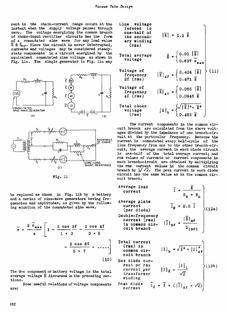
Vacuum Tube Design
rent in the chain -current range occurs at theinstant when the supply voltage passes throughzero. The voltage energizing the common branchof choke -input rectifier circuits has the formof a_ commutated sine wave for any load valuefi Rex.. Since the circuit is never interrupted,currents and voltages may be considered steady-state components in a circuit energized by theequivalent commutated sine voltage as shown inFig. lla. The single generator in Fig. lla may
COMMUTATEDSINE -WAVE GENERATOR
(U)
rd
(C)
Fig. 11
(b)
RESISTANCEOF CHOKE
CORE-LOSSSHUNT RESISTANCE
be replaced as shown in Fig. llb by a batteryand a series of sine -wave generators having fre-quencies and amplitudes, as given by the follow-ing equation of the commutated sine wave.
e =2 eseix
1n
2 cos 21 2 cos 41
1 x 3 3 x 5
2 cos 6f
5 x 7
The d -c component or battery voltage is the totalaverage voltage E discussed in the preceding sec-tions.
Some useful relations of voltage componentsare:
182
Line voltageinduced inone-half ofthe second-ary winding
(rms)
Total averagevoltage
Voltage offrequency2f (rms)
Voltage offrequency4f (rms)
Total chokevoltage
(rms)
1E1 = 1.1 I
1E1 4f
IEIL
.
[0.90 IZI
0.637 ;.,,,,
.
{0.424 lil
0.471 i
{0.085 lil
0.0945 i
i'V1112- i2
0.482
(n)
The current components in the common cir-cuit branch are calculated from the above volt-ages divided by the impedance of one branch -cir-cuit at the particular frequency. Because thecurrent is commutated every half -cycle of theline frequency from one to the other branch -cir-cuit, the average current in each diode circuitis one-half of the total average current; andrms values of currents or current components ineach branch -circuit are obtained by multiplyingthe rms current values in the common circuitbranch by 1/ /. The peak current in each diodecircuit has the same value as in the common cir-cuit branch.
Average loadcurrent
Average platecurrent(per diode)
Double -frequencycurrent (rms)in common cir-cuit branch
Total current(rms) incommon cir-cuit branch
Rms diode cur-rent or rmscurrent pertransformerwinding
Peak diodecurrent
Aid
(12a)
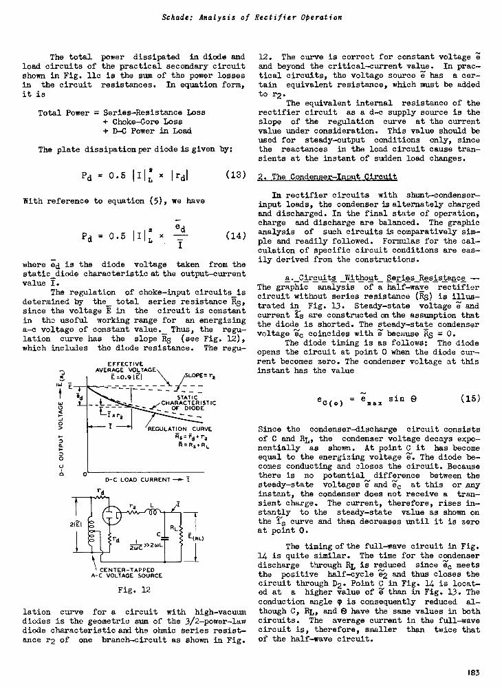
Schade: Analysis of Rectifier Operation
The total power dissipated in diode andload circuits of the practical secondary circuitshown in Fig. 11c is the sum of the power lossesin the circuit resistances. In equation form,it is
Total Power = Series -Resistance Loss+ Choke -Core Loss+ D -C Power in Load
The plate dissipation per diode is given by:
Pd = 0.5 III:, x Irdl
With reference to equation (5), we have
Pd
(13)
eA
= 0.5 III: x (14)
where ;d is the diode voltage taken from thestatic_diode characteristic at the output -currentvalue I.
The regulation of choke -input circuits isdetermined by the_ total series resistance Rs,since the voltage E in the circuit is constantin the useful working range for an energizinga -c voltage of constant value._ Thus, the regu-lation curve has the slope Rs (see Fig. 12),which includes the diode resistance. The regu-
IW
<
0
0
0
21E1
EFFECTIVEAVERAGE VOLTAGE
E /SLOPE= r2
-I- - - - -STATIC
CHARACTERISTIC.1' OF DIODE
REGULATION CURVERs,-Fd+r2Ft=Rs+RL
D -C LOAD CURRENT
rd
CENTER -TAPPEDA -C VOLTAGE SOURCE
Fig. 12
lation curve for a circuit with high -vacuumdiodes is the geometric sum of the 3/2 -power -lawdiode characteristic and the ohmic series resist-ance r2 of one branch -circuit as shown in Fig.
12. The curve is correct for constant voltage 2;and beyond the critical -current value. In prac-tical circuits, the voltage source a has a cer-tain equivalent resistance, which must be addedto r2.
The equivalent internal resistance of therectifier circuit as a d -c supply source is theslope of the regulation curve at the currentvalue under consideration. This value should beused for steady -output conditions only, sincethe reactances in the load circuit cause tran-sients at the instant of sudden load changes.
2. The Condenser -Input Circuit
In rectifier circuits with shunt -condenser -
input loads, the condenser is alternately chargedand discharged. In the final state of operation,charge and discharge are balanced. The graphicanalysis of such circuits is comparatively sim-ple and readily followed. Formulas for the cal-culation of specific circuit conditions are eas-ily derived from the constructions.
a. Circuits Without Series Resistance --The graphic analysis of a half -wave rectifiercircuit without series resistance (RS) is illus-trated in Fig. 13. Steady-state voltage 2' andcurrent is are constructed on the assumption thatthe diode is shorted. The steady-state condenservoltage We coincides with Zbecause RS = 0.
The diode timing is as follows: The diodeopens the circuit at point 0 when the diode cur-rent becomes zero. The condenser voltage at thisinstant has the value
eC(0) = emax sin (15)
Since the condenser -discharge circuit consistsof C and RL, the condenser voltage decays expo-nentially as shown. At point C it has becomeequal to the energizing voltage e% The diode be-comes conducting and closes the circuit. Becausethere is no potential difference between thesteady-state voltages e and "41"c at this or anyinstant, the condenser does not receive a tran-sient charge. The current, therefore, rises in-stantly to the steady-state value as shown onthe is curve and then decreases until it is zeroat point 0.
The timing of the full -wave circuit in Fig.
14 is quite similar. The time for the condenserdischarge through RL is reduced since .1";c meets
the positive half -cycle e2 and thus closes thecircuit through D2. Point C in Fig. 14 is locat-ed at a higher value of if; than in Fig. 13. The
conduction angle c is consequently reduced al-though C, RL, and 0 have the same values in bothcircuits. The average current in the full -wavecircuit is, therefore, smaller than twice thatof the half -wave circuit.
183
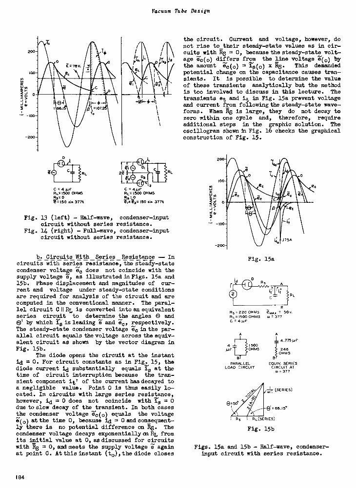
Vacuum Tube Design
200
10D
5
Wyk
2_1<0 0JI
-100
-200
jI
76V.
e,
111 111
66.1 jj°37
16- -.4
C = 4 }ifRL.1500 OHMSas= 0'6=150 sin 377t
2e
Le -212
C = 4pPRL=1500 OHMSR3= 0ZI=Z2= 150 sin 377t
Fig. 13 (left) - Half -wave, condenser -inputcircuit without series resistance.
Fig. 14 (right) - Full -wave, condenser -inputcircuit without series resistance.
b. Circuits With Series Resistance -- Incircuits with series resistance, the steady-statecondenser voltage iTo does not coincide with thesupply voltage W, as illustrated in Figs. 15a and15b. Phase displacement and magnitudes of cur-rent and voltage under steady-state conditionsare required for analysis of the circuit and arecomputed in the conventional manner. The paral-lel circuit CIIRL is converted into an equivalentseries circuit to determine the angles 0 andel by which is leading a and .-4O, respectively.The steady-state condenser voltage ec in the par-allel circuit equals the voltage across the equiv-alent circuit as shown by the vector diagram inFig. 15b.
The diode opens the circuit at the instantid = 0. For circuit constants as in Fig. 15, thediode current id substantially equals is at thetime of circuit interruption because the tran-sient component it' of the current has decayed toa negligible value. Point 0 is thus easily lo-cated. In circuits with large series resistance,however, id = 0 does not coincide with is = 0due to slow decay of the transient. In both casesthe condenser voltage '4'o(0) equals the voltagee(o) at the time 0, because id = 0 and consequent-ly there is no potential difference on R5. Thecondenser voltage decays exponentiallycnk fromits initial value at 0, as discussed for circuitswith RS = 0, and meets the supply voltage it- againat point C. At this instant (to),the diode closes
the circuit. Current and voltage, however, donot rise to their steady-state values as in cir-cuits with Rs = 0, because the steady-state volt-age '46(0) differs from the line voltage (7(0) bythe amount ec(o) = i0(0) x R8. This demandedpotential change on the capacitance causes tran-sients. It is possible to determine the valueof these transients analytically but the methodis too involved to discuss in this lecture. Thetransients et and it in Fig. 15a prevent voltageand current from following the steady-state wave-forms. When Rs is large, they do not decay tozero within one cycle and, therefore, requireadditional steps in the graphic solution. Theoscillogram shown in Fig. 16 checks the graphicalconstruction of Fig. 15.
Fig. 15a
Rs = 220 OHMSRL =1500 OHMSC = 4 j -if
A
IC,
c'T
4 J- 1500
6,4A,. = 150 V.ur = 377
OHMS
PARALLELLOAD CIRCUIT
G=50*ti
A
4.775 }AC
246OHMS
EQUIV. SERIESCIRCUIT AT
= 377
(SERIES)
e=6815*
RL(SERIES)
Fig. 15b
Figs. 15a and 15b - Half -wave, condenser -input circuit with series resistance.
184
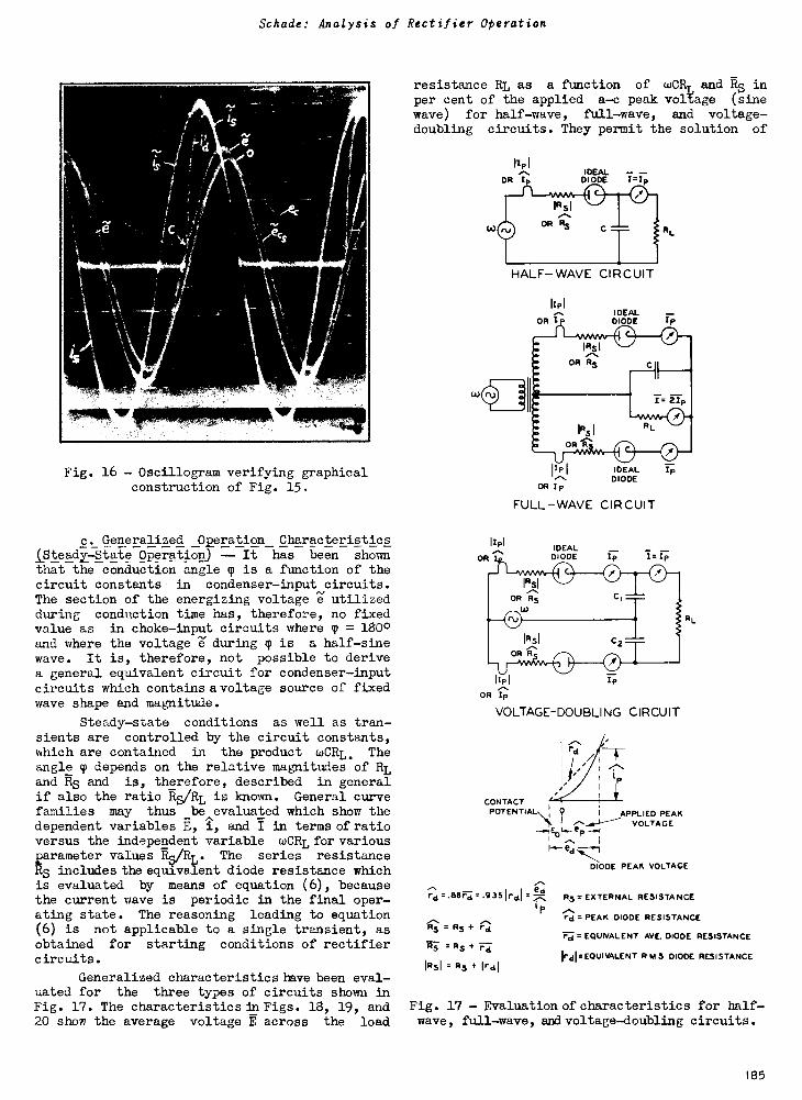
Schade: Analysis of Rectifier Operation
resistance RL as a function of wCRL and Rs inper cent of the applied a -c peak vol age (sine
wave) for half -wave, full -wave, and voltage -
doubling circuits. They permit the solution of
IDEAL - -OR I DIODE 1=1p
HALF -WAVE CIRCUIT
IDEALDIODE
IDEALDIODE
OR I p
FULL -WAVE CIRCUIT
RL
Ip
I p
IDEALDIODE Ip I=1p
1p
OR Ip
VOLTAGE -DOUBLING CIRCUIT
CONTACTPOTENTIAL I APPLIED PEAK
epVOLTAGE
eDIODE PEAK VOLTAGE
I rdI T
edrd = .68rd = .935 rdl11,
= R5 +
Rs = Rs + rd
IRS1 = RS + Irdi
Fig. 16 - Oscillogram verifying graphicalconstruction of Fig. 15.
c. Generalized Operation CharacteristicsiSteady7State Operation) -- It has been shownthat the conduction angle p is a function of thecircuit constants in condenser -input circuits.The section of the energizing voltage e utilizedduring conduction time has, therefore, no fixedvalue as in choke -input circuits where p = 1800and where the voltage e. during p is a half -sine
wave. It is, therefore, not possible to derivea general equivalent circuit for condenser -inputcircuits which contains a voltage source of fixedwave shape and magnitude.
Steady-state conditions as well as tran-sients are controlled by the circuit constants,which are contained in the product WCRL. Theangle p depends on the relative magnitudes of RLand Rs and is, therefore, described in generalif also the ratio RS/RL is known. General curvefamilies may thus _beevaluated which show thedependent variables E, i, and I in terms of ratioversus the independent variable WCRL for various2arameter values RS/RL. The series resistanceRs includes the equivalent diode resistance whichis evaluated by means of equation (6), becausethe current wave is periodic in the final oper-ating state. The reasoning leading to equation(6) is not applicable to a single transient, asobtained for starting conditions of rectifiercircuits.
Generalized characteristics have been eval-uated for the three types of circuits shown inFig. 17. The characteristics in Figs. 18, 19, and Fig. 17 - Evaluation of characteristics for half -20 show the average voltage E across the load wave, full -wave, and voltage -doubling circuits.
Rs = EXTERNAL RESISTANCE
rd = PEAK DIODE RESISTANCE
7; a EQUIVALENT AVE. DIODE RESISTANCE
KO EQUIVALENT R o.15 DIODE RESISTANCE
185
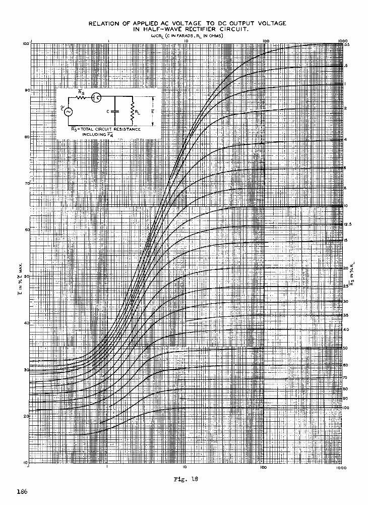
D
1 lllll 1 HM1111111 1111111111111, llll 1 1111111111 llllllll ninn .1 mm 111111111 lllllll 1 111111111111111t,ll 111 1111111111 lllll HII 11111111111111 III llll 1 1111111111 lllll I 11.1 in 11 l II 1111111111 llllllll 111111111111111111 111111
M":".M1""n.1": ll IFIEE111 llllllllllllllllllllllllllllllllllllll 1111111111 llllllll M1111111 11111,11
1111111111 lllll "111:1911111.9
lllll 11 1111111111ln 1 1 I I 1111111111111111,1 III1111111111 llllllll 111111111111111111.11
111 II 1111111111 llllllll 111111111111:111
l n1111:11111 lllll 111111111:1111111111111111 lllll I 111111111111111P,
11- lllll I1111X1 . llllll
lllll llllll iiiii 111.1111 :1111 1 I 1111111111111:11,11
11111111111111,111
llll IBLI U111111111111 I 1 1111111111111 1111MINIKIN11141111111!...111113ifin mei ni lll III 11111111 lllllll 1 II 1.111 11 11GMME 1111111111111 01.11111.11111j IIIIMIM11,11111111111111.111111111 lllllll 111111111111111111 11
l 11:ECNI: 111111:111:11FdllIE inn1111 1111114 MINN PI 1 II 11 111111 '111/11111111111111In! 1111114111 inn inn Will. 111 I inn 11111111111111111 :.
llll 1111 IU1111111111 111111111lllllllll !miim.....Nonio.:111 111 NI 111'11111IPPI"'"'"'""1ii 1 1 111111M:11p:1 lllll 1 1111111111 llllll I III 111111114 1411511.1 II I 11111 1 11 lull .11 1 I I I III 1111,111111111 -..1ILINI111111.1 P1
llll 11111111111 lllllllll ilin.11111 1.1111I111111.111. 1 1 1 111 11111111111001111 /1.1.11111 lllll 11_____. ll ii/i111111 lllllllll 1 111111111111111 11.
rl: I:=I 1 11 IIM'1111111 71111111 lll linrimilionuiummillirmililllinIMEn111 NI 1111111111 II1'd ...,111101MMINE_g Jilin,: llllllllllll 111,11,11,1111,11:1111
MMEMINeMILI llllll 1111.1111111111 1111111LiiriVarillenimp 1 ullilitanHiln 11 1111111111 11111111.1: InBillienr,1111111B1,11111111111111111.11:11pg 1 11 I:1111111111 lllllllll 1 1111111111111111,...nam lllll niluifti 1 411111 11f1 11 1111111111 1111111111M1MOlp 11111 I I 1111 1111 .1111 llll nii ..minima 11,
"nff."21.11." 111."""rdirIlli;rin1111"""ilgiii::::: lll :Hill 1114 11"1 Iiiiiiiiii:H19 lijil 11:::::::".1 ..ItiEEP:- llllllll "::::::::E:11.11;:::1:lllll m ., Nil innullaimummisimulin gilliii"ii: II """"""iiiiIIIIIHII: g.'-'1"--,, ,
l mum!, lllllllll 1,1111,1111111111.1.
.. nu In. 11 1:1111119:1W I 1,1111n1
l 11 1.111111119 1111111111111mw,...mm-.'' nnn...11 ..1-1111..1...... ,. 11.1 11 Ittli MEM11...:14.114h.:1 ,11214..,
iLt ;1.. orii.:;;; ll P_4!,.,,dr,E.;iii;EEllml,H .1l : lllll
....MEN112.1 111:11:1[111111.1111111111111111111101J1":::
.ILA 1 ..11j irdia ..zinlyi:..tiiiiEN,r.-"."EllErli;:::::MEN.:::11 [1:1111,::1'"""""1111;111'=,
11111E1;11iii:g11gqi[liiiiiiiljurudf,'"IN%' E-E:-...::::1 lllll 11Prillill llllllll 1111111%..i. in 1 11 e.,. .,,41.,,,,....1 , llllll 1111 IN 111111611111 511111.1.11161111 ii III 1010101
O I 1 I 11 11111 1111114'1111112:111;111411 11 II 1111111111:123..tr.....1iIrl11, 161111iirB \ IINUI I I I 11 1111rIVIVI llllllllll 11111 11111,11'All;1
01
11111111111T,IVIlt FIF11111 [11!!,"'riiiiria llllll i:t1:1[111m"11V 1::::gEnl:"" kIiii.liH111 ":::::1',1:1,11,11...II.. iiaixAr ArAras..!_ui.....iimilimiu llllll minim,' all:Iii mmmom.. mil
I. ..:.,.11111H212'=""''';i1 11 1111111:11E1111..,..11111t1Paii:""'''' llllll 111:111111k0 11111111111111,111
111 11111111111111
111111111111:111
MIMEM MENEM.
alL111111.B IN ..1 1
r:1111if...1:NZ llINIM111:D.. 11111111111111111 lllllll 11111111111 WI
l =11111111111:111111 1 in II 11111:1111r1:1111::"" lll111111111111111Ullll 11111111 111111111111111111 l
:1111.11 nin." 11111:1
111111111111111111 ll.....N11 11111
111111111111111114 MN
irIMIlliliii:::1111iitUq11111 1 1 Ill IIP'11"111li'''171ng. II 1 1 11
l 11 11/11
II III nil111114 MIAMI 10111M1
1lll 11,01:111,1
111
...I 11:111111117 ll 111111111111;1601: ....al ili11111 lllllllll Inn!! 1111 111 :nimm
/RH 11:h9111"EIZig'-r-111:1 lllll 1:111:1 IHI:i opENEftla::::::::::N.I..,
... ll N11 1II "
igEllIY
n::- :HullII HIM!
:::Er:: ll UN EMMM.M1111M.
en1.
Bill M.
or 11:III llllll 1 ill 11111111111111
nudifiliNilifflllll nuagri: II
"llh P 1.1h H, ,111711" '''''''''nelialimpir.unFr.m!, 111 1 a llllll mum. mi
IIIII 11 N
lllllllllllllllllllllllllllllllllllllllllllllllllllllllllllll
giniffillnigrdi .1 EN 11"-i llll 1........,11Mitg11111111ENtia1.... l tom....+Awn 11
menneenninnnnnnm
ll 1111111111111111134
1111111111UM
ISMEMEN1191M:2::1111.ii.i111
MME lllll U ligill=1111M11/1;"'"
.
:Nam 1 .
ow !pun! monsa 111111r1,,RINPiIJIF111
liprairdERFFEril:111F, IZ Fir.
ll
ll
1M7"1',,
tp.lnuIx111
m. ii1.1.1.011111111111,1',
::::::llllll_:w7p111111111111 111111X1 1111
l - .1i I 131111111111,-...
M,M.11,15FAMESMEMOS
111 I I 1111 11111111 lllllll 11111 1111111.111
11[11411i19EEEirdliiriEiN:11111111MEMPli1110111111111,1, 11.1011iniiiiiiiiiMilliiiiiiiiiii1.1111 111111111117
ffill211R111 l :11:imamova lllllll
EfE EE- lllll ll l
111Il1Ij 1111111111111 II1t, 1111. ::::uun 111111 'L E,TEIIEEE:Em11:1:
lllll
v11111,1,11...I 11.11111111diil
Ult11111111,11111::
IEEE!: .
111 II minnow,.115/1111.11f11.111:41.11:11,
11111111:111111101u
INUM" 114:111411
1C11,13,1',P '"`"illOrrpTe!'"i1,1=lll m11'11011 Jjp,t1111
llllllllll 11111111011111 1111 llll NErrIV2IIIIIIII:Irlitulin 1,91
.a:. lll n'il'i Mi""""'":1:111:11'111 11;;;I.Vira?"litInIE IN,,,,,,,.... lllll IIllmmalla 111111.11111111 1111111,111 Ill
IUMM IIITJIIIIVW
H1.11111111111 11 1111111111111 111
11111111111111,11L INIMEN1111111.11/1111.11.11..111i1111r111." lllllll '"P'''''INIPTAIT. l-- : : :: :::1::-.
/Iii 1,111,B1n111.11 nAil 1.1M1a2 . : .... :il: 1 II:Eil ....Wrin 11111Q11111111111111111111111111.
ll 1 .1111f ir,1111,11111I
IFEJ:=11111I
llllll 11 11 iiiiiirlilYRFIIMENIillifOrVF.1.1.11 41111411.. .11 11 11'HI.......9E VII! lllll n11111111111111,1AULMM1111 1.11,1111.11F, ...-,....,..ram..4y., 1 il
---iii-....'"1".0ll r.Brmin:FiinBilinIer.1 111111111110111
"int 1m=MMIIMIN111111BaliiiWM l 111.11 1 1 1 II II inn 11141 Will 11 111 1111.1 earl/// IPA A:MI.11,111:111 11/11 lllll I LI, 1,1111111
lllll 01111114112111111'//0 /111d11gpill11.1111 INAiii-11zur lllllll -E-""1-ftg!:::::::rli;;%.,..prr -.9:!^i.iarargla.-n-pliniimim.---giii-g-iii
eine11.11 111111111 opmannowr V , 1 AIM 110 1 ,111111161.91111111 .1q.M.1lMMU
11111
ISIIIIIM4;111111.1
111111111411111:11=U11,1111M1t11:rrlifir.E1 11 IMININPlii111111111"."ell"
gDE11,11.11.11.4._11111
n 1111111111 1 1 11 1111 1111111a MME ninviu MC
ll uninnoimagi nnin 111 Ira '4 lllll 1111111......111111111111tilUdU11111T11111.11111111111111141//, l '111111111111111111 "
1 1 III 111111 1111'1/0 AN, llll 1.1111111111 I 1
"
lll 1 I 1:MI11111111
ll utilmulnummEm:::Erz, Well,1111#11,111 1 1
ll lllll 11111111111.111,FAI.
uA
1..nini.11111.M.MWERN
llllll 111111111111 llllllllll 1111111,11. 111 I./A IF llllll 11111 111;1 111111111111 111 mIn1111
111110117.4.144;=
l I II 11 !CHOI llllllllll 1111,111 .11,.1 ma ll 'n1111111,11 1
nyinil1111111 u 111141111,11
ll ll l .a.n.upp.wommeenTE!!!.22---T llllllll 1-milEITOIrikmeiNEEEEEEE 111011'""1":1
RN l111
ilinn.,- %ennii...11./111:..11,1 mA ' immNE-Nzama!, lllll ni1 1141/1M.1+,-.0!;:.,1;:;:;111,17'..,.., rit11111.,ff.i.4111H1 Hal
aEiii l ii l iiMill!2=1";iii:',".W ;Ai lilnii!I''''""' l 'filAweiliiililliHritil,"1.2:a.n;imEE,r,g1r,11:11:Hugui:111,1t=iiiimmeims21,112%..- :... gmEnt 1:11 lllll :wpm
Benin.-- 11.11,1111, 111111,111111r 111:11iiallECIE'"""MM l
....111...:IIM11111.11.7.i.M11.11.1111111111P7,,d1111.Mr.E',.,"!...1511:191/r141Ealt.IP
minnipl,....111111111
lll i: B.." ri;iiiig is 13FA!!:91,.,11F,11 istiiiiiwiiiinnilliguinillill;i.. l ......, tn4,iipriiiffil!..0,1,0.1:
...41.14 ....11111111Alifl, . ._711111ritir IIIHRINE111:17:111:1111q1.1:11l Ntrit911n: LIM int: gr111:11M11 lilir :LUNN 111/4.11T11;;__1 ,nel elennli Ell 20:::111 AN IMMIMarl11211711
Mill lllll Lilli lirt11401 1'11:101111 fil, 'al 1:11102r; Mr. 111.1a1M111111:1211L111Ilingfillin2 Z
MI lll LI 1 1 11 11 illuill.111 I lllllll .:.,----.7.-..Ind,' 1,- qiiii11111 II mr ''' ll !'". l ""illinTllenlifir 1"2"11"..n..
!,H!qui iiiiiiiiiiii1014r.s gm' :,4:cquiuml,iiiiisiligigfi,XIImEmp.ejwiLipa"91/1:11;1111!...-ag:qiii'i5;-.....naligiii.lpnoir.....1.7.--:!:
1111._ IUMIIN
IMME ll l 11111111E" 1111111111111. 111111..1111 litk:1 InIn 11" IllinLInt iiiii-:---..imigli..1:1:HpEf,,,.... l aE:EE: lllllll EEE:------ l 1;igElf.P.,11::: nEn'iiiFE::::112.11111111111111=1,111NMinn III Hall ibildm
II lllll 11111 11111111,111, M.MENEl. i
;. -E.,:::,11, llllllllll 11111111W111.111"'111'111"""11"
in4110111111MM 1 11 .11 PA' igirrig V 111.111:4911gli , '''' ., I, :
llllllll 1111111BI 9111111111111QM:"...''"Wi U 1111117 lttttririt lllllll 1111111111111:1111u ...1IN111 1 1 I 1111 lllll
JI
1111111 llllllllll 111111111111,11 1111111111 llllllllll 11111111111101.111.llll 111m1111,
111,11111
1111111 lllll Hill11111111111111101 IOW....MIMI:nil
,111.1111111111 1111111111H111 I 1 1 1.11111111111114111111NE llllll
llllll:kcivinEREzt. 1.., in11111111.11.11%111,EMU
llllll 1111111111 llllllllll
011111 111111111111d Ill 11111111 1111111111111111. l 11i1M1 111131[11EVITHIPIEFYH411:Mr1:121111111 11111111411111dlemmax1111
- l 1111111111 llllll "11111:111111N"'
111111111111111111 1111111"p0111'111
ll 111H11111111 lllllllll 11111111111. 111
1111111111111111111 1111
1111111111 111 MN
:191142r1111:EFUSIRIE1111 n um Nue!1111111 lllllll I 11 1111111111111111.11r.111111111 111 111111111 '1. ME
111111111111 III MN
l th. dig'1111111
111sim 011111111 1 111111111111111 MEI lllll L11111111 1111 llllll 11 1111111111111111111.1111111111H6011111 1111111H110
HIIIII
1X111111I lopllllllllpqmi111 lllllll
llllllll
1111111111111111111111 lllll 1 I 1 11 1111111111
11 111111
llll 11111111Lp lllllllll 1 111111111111111 HIM
llll 1 1111111111 llllllllll 111111111111111 111
llll I 1111111111 lllllllll 1 111111111111111 114 1 11111111111111 1111 ll Irj:::1141111.11 lllll 1111111111111111111
11111111111 IIIl 1111 1 1 I 11 11111111 II III 1 1111 1111111111111111. Mulllll I 11111 I 11111111111111n 11,1 ifill 1:411 1:11-E1111
11 III I 11111 11111MM:111, m qnni
3111f1INEEEEErri,,IP.'1:42..e. 11%1111111111111!" 1111111141111:"21lllllllllll llllll llllllll 1111111.! " TINIllt111111nlialru
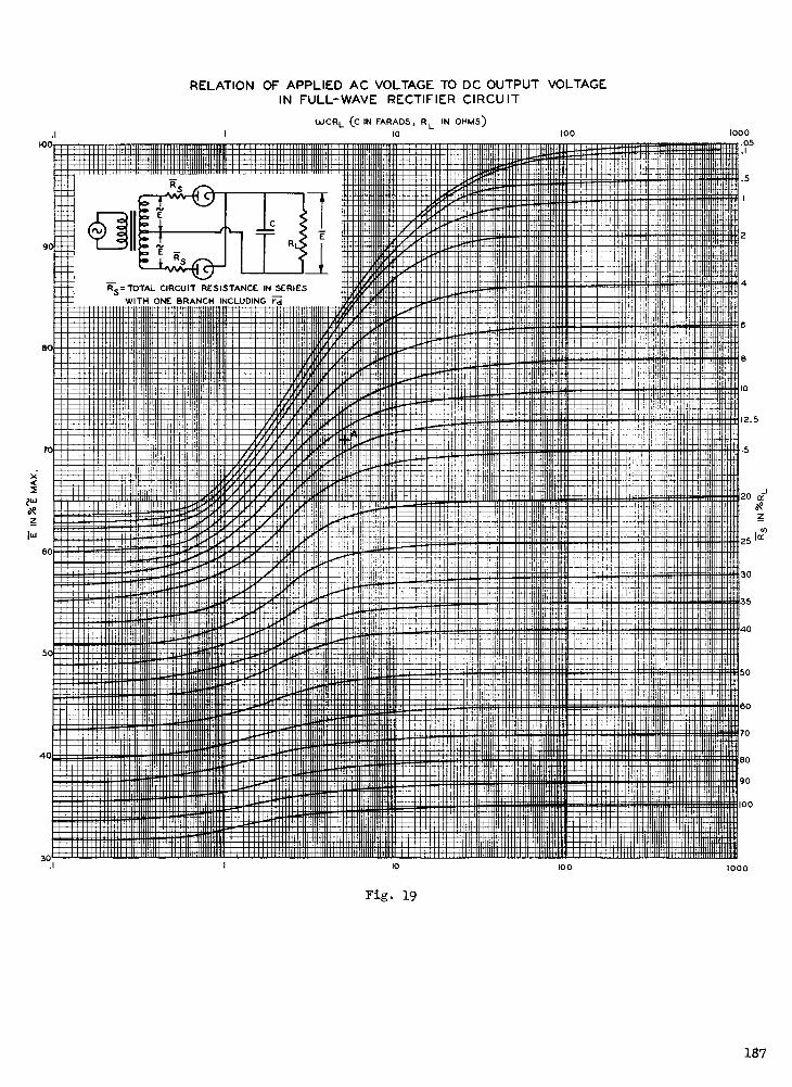
' ""' I moms:U 11111 III lllll 1111014.1.1._.llllII 1111w111llll 111111111Moll 1111 111llnnIIWUllllllllll mummumnll 1111 III llllllllllll nunumninorm-lllll 1 m lllllll NI ll muun
inimmu 11 lll .11111111111lll Loihnunnan
11 111111 n llllllll H1111111111111111MII 1111111111111111M
1 111111111111111M
lllll num lllllll I I un miniumll um [ lllllllllllllll mum noon _111111111unumumum
i i ulI 111111 IIIMIIIIIIM
ll IUNNI lllll 1 lllll BIM MI 1,I. I iilnr111111111101911111ll 111111111 llllllll 111111 1111111111111111111
MINIM 11111111111. . lll . _.,.__IBILIIMI11 lllllll 11111 WI, llllll I. II MEgramilla 11111111111 1
muffling. lllll 111 III NIMIMEl II 11111111119 .0. 1111111111M111111111111m11 1 1Ii 111111111 lllllllllll III UIMMIIIM
111 nuiwommiammiull !.. :Zig l "M 111 lird_11120111110111 IMMIMMIMII I 111111 11111 IIIIIIMMMOMNIUNIMUNKNINI11111111111 lllllllllllll11 1 1111111 11111111111111111111111MINUI$01$1111 99 - 111111 11111 -am:: IIEN llllll 1111111lllll 111 11111111111IMINMEOMEW., 1' .$1111111INNUI lllllllll 111 11111 IIIIIIIHMIN IN llllllll UIMIIMllll 11111 num wwwwwwwwwii lllll nm lllllllllllll iin 11%
11111111
lll min winumwimnisor.so.donnimiwu i111111 H 1 .,. n
lllllll OUTMAN!lll I 1111 11111111111111111 IINIMIMIIIM 1111111114ll M I I
.., ....71
lllllll 111 HIMINIMMEredIP.$111§1.-11+1 1 1111111 II NIIRllllll nu iniffinntwormunwasemmuiiii w I mown' num WM 1111111 I I
11 I PIM 11111111CMINUM11911111111111 111111 1111
Mllllll 111UHUll 1111
llllll 111111 111111111111MINMINP_WIII1 lllllll 111111 II 9999 111111 MUM undiummorllllll 11111111111,111VAMr.MUSUNNOV".17, llll h..a . miliiii =IT 1111111111110111 UMWMMillllll 111111 itimum,ay.mito.som1U lll IH N11111. MIUME MINP-MUIIMMUMN lllll 111111 11111 11111 IIIMMIII I 111111 in alUNIIII 119,111111UMMIIIHr 111111111111111 1111 11111 11111M
1 11111 1 IP MIIIIMMII
1111 1919M1111112t:9991121110111911 1 hHIMICIiiill 111111M11111 11111 111119 II II 1111111M1111 11 1111 Ill I numb no
.... rokLooraoluilipeuipqminqui Millibinli Ililliell. ...11111111111411,11=FilIMAI.. ,,.. . d...... . .. n ,n1 1111 1 111 111 1 I lllll um
911 ° 1 lumonsoralluenerz..liummunms mrir.i neseit ishigiiiimiliniii,,,, .......,..m......,......... 1911 U lingli 1 Ere . M 111 " M i1 II'. 111111111111MMENNUtIalfle I
1111111111111I Al 1 ' 111111111111111INIMANNIN IIM 11 Ing Mi MIIIIIEN MI 111 IIIHM111111111111 /MU' I all 11111111111UMEMIN
1111 11111111 lllll 9.1 I I 1111 9 alIIIIIIIIMMINIME 11111111U H llllll 1 llll no mmmannowasousson
11111111MM
MAR
llll 11111111 lllllllllll 11111 11111' ..11111110111M MN ign in in no 1 nu umnas i EP.is llll llll 11111 1 11111111111
111111 H11 1111 I 11111111 lll minium, llllllll 11 I II'. 111111111111MMENEjlhaii0611.1nUmrIlm111111 ijuhiluizral....is "iwinneTas:
1 1 1111 11111111111111111Pnall0=11111111 11111111111111111111111.-27..ON
.111 111111111111MMMP 111.1111 FlIrfflial 1
II lllll 11 111111 lllllll U 1110111M111111111ll MIMI llllllllllll IIINI 11111111M1M11111111111
III 111111 III 111111 111111111NEMEMSENNIl NI
111 11911/.11NI 1.119119.111111111.19.1/.111 lll
.1I 11111 1111111111117......
9:4111Mgrgge 111111111111
11. -ir-iumummarilliiiiiiiIIi 11111111111...........1........... llllll 1111 1111 11U 1 1111111
111111 UU IIIIIIII 1111111HIMMl ,11'111111111111.NAMUR, 1 1111 111111111111
al 111111111IMMEIMMEN
MMIonnouni ii
un ii min lllll un mum 111111/1w i inin muumuu MIMI11 II HO I 011111111M
lll W11 MIN/ 1
I11 UN, II . lllll 1 1111 111111111111!:=101M1111'141111/1111111111. lllllll 111111 KM ,011INMINIIIME
. lllll III 111111111111MIMP-mHIM 1011pgriugull'01.91111...nnoui
MIMI IMI lyll 111111111mi. limilimmon Jo=BRUN IMIN1.111/.11 IV.nn 11'811 l 9/1111 .11 IIIHMINIMINIMUMENN His/I:=111N.T.NN4.1111 1,1111M.....1.1.111K
Erir ll 1111111ll III il NrIg
HUH
MIU :MIX I MI!
111 IAMMIM
ll ow nW M
IM1111MEEM
idupirp de RAH puff.........,..:-.
P/1aill U11:11:11.
1$1 IM11111111111111MMIM1 9111
ryry I 11111111
MBIUMMININIENNialillMO
EEC,IIIMP.I 4,111.111_11 IllUINIMINMAIW' IIIIII1_ 1...111111111
ll .11.1.9,117.1111.1.1 14.1 7.n .11 OM ...grimushuili Wil 1112121
umI
1
in
onismounissiOnin no
mur.rammu, lllll 11111H1td1111 ?ell.'NINIOAVABI IIIIINNIIIIIi 119 1
,AWIIII ..1111rIIP'61111 11111 lirgliiiini Hi Ere111111"1
u ulli 1 wilMM no unigi i:1 milswIremIlloinMilli' Iliwwwurairnar.0lllllll mut.,.......,
ItgrolostgarisISAVIIIIPANVA11,11 H
V. .1 II
il.M.M!!.....MUMNIMMIIIIM101
MUUMUUIMMMEE
HI ihmirmiliiiiiin illiiiiiiirdh ""
92-0.......11WII9.119.123,111 lllll NI: muumuu
diwAr. MIN, lllll iligligniiff wwwilmouminim' mwmasuuumn1111 iminmwimanosom
r991 HUM NMI11111111111111 BUHL IL nnia14111111MIE111 lllll 11 MIN111111111
IIIMMEEMEM 1111 H111 11111111111111/111111
111111191, Forrawaralorailq... ...
11111111111H1 .11'.11,1 .1 dir.w llll nu dinn
.111 1111M1111111111M11111 O. 91 quigingum sum maw M. PAH MFAMI r AMP I llll 1.111111111111U11111MIESININIIMUN 1 llllllllll11- 11U111111 N1111111
l II 1 MIIIIIIIM
zgegeringnordi WOW ;R... 4 pronaAwramor, ilkilin..1 pooloPilidlifi................lll ...r.mreap,..::.0,06 r,Lleco:onsurid 1111!..agi U -U... ......1111 11 lllll MI1111 I it.
..... lllll MIMI 1111111
1161UMUUJILITIM11161.1".6111°
MeriMMEN11111.111111111111111;10K1110gggnalg;i
11MMEMMI 111101111111MEMENNEMIn
MUINIUMNHIMME111111111 U1 1 I: ii 1 LIMq ill ull UI I Oil
r. omiNIEleliMMIENIUMI.111111111.11MMLIMMENIVAIMILMMISIMIMIIMMEOMMg Mg MEgg 11111 111111101111111
Mill !!niiii 1
mum 11 !!!!!!!11 III lIIhI
dill 11111
-lllllllllllllllll ::::'" llllllllllll imillimmus- llllllllllllllllllllllll Mg 11 POEN"' lo UNI
9 9911111 III l 1111.1...,..,U11111111111111111..:
l llllll 1 1111
1919111!!! llllllll 1111111 1111 iii lllllllllllllll11111111111111111NENUIn-- 10111
ll MI: it; lllllllllllllIII:
11 iiiiiiiilliulliLmoin.= 11.7: l num llllllllllllll nu null inm nun1111 numum nom
um nu n1111111111
/111 /111 III n911111 11 1 IRKIHN11M111...- llllllllllllllllllllll 1111 111111 III M
l 1111111 lll-1119191
!.... llllll Itiiiiii111 lllllllllll 111111111111 IIIIMMMEEMMIIl 1111
llllllll 111111 llllllllllllll 1111 1111
..nti111Mmlllll UMMMM1INCIMMulM1411111:1;1111111111MMON"un''''111111w wwwwwwwwwwniiiinnunoull MO MUM W. di
n -rntiMirrinu""11d111,11E:i11111iiiiggnillnl'iM11111111111...MEOHM= lllll guningmrs,,,, ..,,..,,,,g1IIIMMUglInallINISUI P:1111111
l 11111111...::i011111111111111.111....9.92i:;..nrrg. MUUMUU..00111Nl IMMII
l IIMINI 11111 .",$111111MINUM111111100' 'l MIUM111!: .iii IIHIMIIIIINIMMUM: " ll HIMUI11111111111111111M HUMOR= MINIEE
niiinunu um 11110r1'....- llllllll IMMIMMIIIIIIIIM 11111111111111111111MMMllllll Vt 11111111MINIMIM HINIIINIINIIM IIIIMINHM 99991199121 II
1M iiiiiiiiiiiiin m mum111A ppi MM.! EMI
11111111111.- llll III 111111111111MMP! l '1111111111HINIIMIMINIUMIIM11111111.11111lllllllll
l 1191 99th llllll Minirlir.'.7' U lll 111111101!- lllllllll 1111 1111 1111 WMIIM11111 1M l muffin rill
!!! in1111111H1 111111111H MI NUMIII 111111 N II 1
111111111 III U 1 111l - llll 1. llll MIMI lllllllll 11111111111111111 MEMIM111111§11111111MI.
lllllllll IIIIIN lllllllll 1 ll 1.r.1.1.11 ; T11 ...:11.711101annul unim:111111111111m11112E111111-11-...41 lllll m. %lamiiiiiiiilemt 1111 11111
n llllllllll minilll 11111 lllllllllllll MI1111101111 MIMIIINEEMMINNIM! ,....,- lllllllll 1 IH 1111111111
lllll 1 ll ilklllllllllllll 111111111.11:1111:MP!'ill:L.211...., _1111111 111 MMIIIIIIE
111111 11111111111 .11 w"11511111111111111111ffillErUIMI 111111111 lid MI91"111. . llllll 11 11111 1 I III 111NINIMIHN l MU1111 lll 1111
lll mini. lll e! lllllll iiiiiiiiii=1 II 111H11111111111111111MMEEHE191991111611111MMMILMI
111151 n1.14 FPIIPNMI 1111 111111 111111111 11 NIEMEN.. mum 11111 1111 lllll 11 l 11111-1 11
II 11 ID 1111111
1U1111111111111
HUM II ersius m , 11111111
nail ow
nomnumumn- l
n TH mono11111111111
MAT1111111weglaml
1111111111111111 MEllllllll
N.IIW 111
31111.111.11 111
1111.1 110,11111g1Millm
sum6Innolommilti 01 ImInu umnimulunm 111 1 it
111111111111911111.1---1111MMIL 1"llll grin: lll I l
11111 I 11111 111111111lll gig nun 111 IIIII99109911111111121M.
.11111111111
11111 1111111111lllllllll 111111 llllllllll 1111111111111 11111
111111 11111 111
U..11169.111191119
ll 111M11111111111
11111111111111111111M1111111111111111111M
111111111111111111110
uliurninmmin WI
l 111111 llllllllll 11111111 1111 III1M111111111111111111M
1
l 1111111IIIIIII MI 1111910.
llllllllllllll 111111111 IIIlll
6 llll lllllllllll 111111111M1111111.1.1H11111111 lllllllllll11111111111111111111N91 ll 11111111 llllllllllll 111111111111111111M
ON 119 IIII W MIMI! llllllllllllll 11111111111111M1l1 lllll 11111111111111111 lllllll 111111111111111111111MUUMUU Intiffiu lllll un IIIMMILMMMUNIMINIM
MOMNOUNO MB-MNEMUMg:
ME MIME111MMIMSMUMWNUMIMMMMMMMNEMIME1MMMNM=1,1
z
60
I I
$ $
MEM
1111
sraillunigiiimmoggierai'c vccor.pip-
- EgrolurammiStoorgipexii ur\IIn .. MINUS ...1111r
INM/P:0111q11 M1111111..M111111111101 i11011 MAIMneg. llII11116141N9911Mil 1 -ames
nowPROBE
1111111 II lll 11111111111111111i1111111111 11 111111111111111119
l1111M111 111111 1111111
lllllll HIM I 11 1.1111111111111111111111
llll 11111111iiiiiill11111 11 llllllllll i !minimumlll HI III llllllllll 11 1111111111111111MMININININI.:
NMIU 111111 U111111111111111111100111!.."
NM 111§011111111111 11 I III I11111111111INEH lllll U11111111 lllllllll 1 1 11111 llllll :11.111,1::::::M 11 um III llllllll 111111111111111MM .,, lllllll 1 lllllllllllll 1111111111111111MU l ll n lllll 1 III lllllllll 111 1111111111111111MMEIN11111111 IIIII III II 1111111111111111919.ZZEn lll 11111111 lllllllllll 1111191111101 is
9.1111111111 l11111111111llll 111111 lllllllllll 1111111111111111111M
lll 11111 lllllllllllll 11111111111111111lllll U1111111llllllllllllll 1111111111111111
llllll 111111111 llllllllllllll 1111111111111111ll 11111111 lllllllllll 1111111111111111111 MEM llllll 111111 lllllllllll 11111111111111111P
111 1111I III 11
ir 1111 l 11 11 111 111
11111 lllllll U1111111 11 111111111 111101111U1 llllll II 11 1111111
llllllllll UIII lllllllllll 11111 11 1111 11
III 1111 lllllllllll 11111 II 1111 11llllllll 11 1111 lllllllllll 11111 II 111 1111
1 1111 1111 III 111111 111111lll11111111101111111lllll 11111111 11111
0
60
70
80
90
100
1111
n 11111 111111111111 1111
n HUI 1. 1111
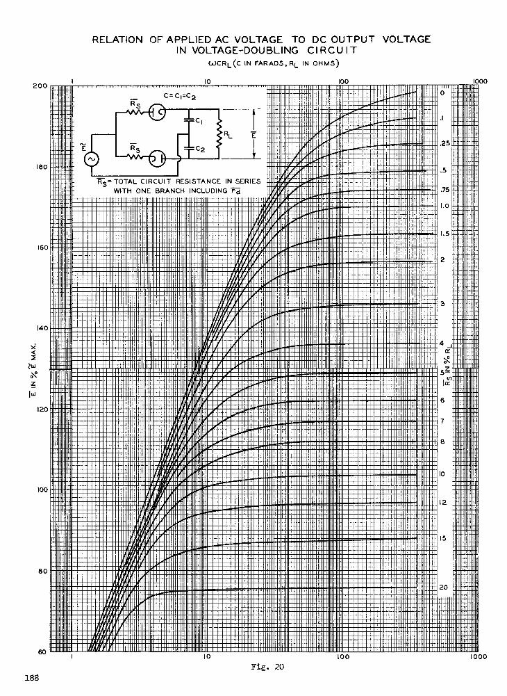
it
hi
m
10111 I
IIIu 111111I no II,
I' kli9m ou .
. . . , 0 III : .- D
. -...... MIMI IMMO . MINIM II 1111111111MII...... . nmui I H HI
.
1 ...a.
........M.gramium"Inin No IIIINP.MUMMINEMIN
1111111111115151
ummINIMIll HIUMMIIIMIumnummu 11111111 MIMI
JIMMIE
1111111 MEI
Um IIIIIIIME UP illCuinnumnrt g....-iimaariom um HolMr' II U 111111111amilr 'I Pri-
mmii nuipmpul .
.urn.I' Ion 8reiort....1,61,46;Vi _.... _ ..: . .....,.
1 Hilluii1111AA. elmodilmoAranumido mm. &pill in! 1611111W
. iiiiii iiiii 0 1111 1 WmPilm Mum 11111 HUI I 1 imam ii iWIMPlui 11 riAluingiurNIMMOI. 111111MINII
011111111 1161/AMMIthilail
NNIiillsili
i tr"- Nri2 1 - III NiririoNNINIMIll
nun ill 11 &-
WY 1,11111rall111111r111 IIIIIIMMEMENmommeIV difilaa511111111 MI . ?....ii ...MN u iii lin II
hind:rim ::-" °°°°°° ". °°°° conummummumum in mherassrawashaLipd.iriiillomitt" El -111191 1 .1....., filmil
Wed , M I rillIII 1
: I
inil NU9 ii MENIENEMOBT1111111mi 1 1 MI11111111111 I ulli liM IIIININEENNINIIIIIMMPAIII !,41 11111111 ,..mcit onI 11111111111 INIIIMEIMINNIIIIIII JO ill?.I p !:. niurii 11 MI
Mt11 1
111111 HEIERIEEENMINNIIIIIIIIMUll IIIIII llllll 11111M IUMMIIIIIINNIMIIMIENIIMEA1 di II ,d11111111111U11 RI 11 11111111MMUM1
III I 11111 111111 111111111NEENINMI lllll ?,19111 am IllInialliffil II I 11111111
1111II
H111 111111 1111MMIMMIMUIMMAI 1!,4 l IMMIIIIIIi1111 1 I 111111111MEIMIMIMM 1111111111 III I
1111 'III MNIEENINNIMIIIIIIIIIII11111111111 11111111 1 MI 111111 MM _RIMAIMIFELD111 I HU 11 II 11111111111111Eall@III1 ILINI11111111M 1 lf
i I MMNIEEIMENNINIIIIIIIIIIIIMIIIIIIIIIIII11111 1 IIII 1111111111MEEENNEMIMIlardWg 11111111111111 II 1!! mommommm.mil- 0.11 -II IR
mu!
um MEEEEMIIIIIIIII96111.111n111111211111111111111 II I 11111 IIIIIIMMIIIIIIIMINWAI/FINAINIuli 11111111111......li H Iii IIIIIMINIMMmuummommssommomm, 'arm immmum ji ...moms!' min
imallINIIIIIN Ul 1111 i i1111 IIMUm l rwminumm" Mini. 11 11 I 11111m1EmuNEN OM MN
rye:: ll I I miimIMMEEE111111M11111d
lIl
Iii I1 1
1 1 111 II lin
1111ill milillI I i il hi mi ei 1 I bini ii II I II pi i I I pi iimil ils im llll llllll illli iniii I I /01 I killilummi mm1 1 r& rh Lpti g pi'i q hi iii ul I!! 1 im II u im II II hi iii 111 1[11 11 ii issm Hi .1 nesm m1
1 mum am lllll um mummum 10 II summoommmrsrawAnemum" immunumm i 11 1 unimm..m..
ll 11111 11111 usommommogrormurAnum 11111 MEM
IINEIMMINIIIIIIIIIIIIIIIIIIIIIII1111111111111111111111111 1 11111 11111JIMMENIE/W5MUMAIH___111 1111 lu aill1111511 1111 Li IIN 11111MHOM1111 1
ll mgm lllll min llllllllllllll 1 mu mis MMEENVIAMIln MIMI 11111!:- 1 MI MIIIMINEEEHN ...rd sun
H sommmmusommummuummumnimmmunamm 1 mu inomemmmrcrAcinimmuzum-4 111115111111111111 III 11 I 5 II1 I minioNMEMENNOMMII1111111111111 NUMMI 1111 1111111 11101 MEIMMIliirrarAMUnilldt nuliMIMiliii i li t 1 nimmimmmsNismm 11E11111 lir .... .1
tur;Of:ram
Iii nommmummumummummi aim11 ommommommommuumm min lllll 11111 MI ill)111m11111unia1151111111111111 1 nummummum I1 111111111111111111 11111111111111111 1111 IHI Hum m I It I AM '.111111111 _1111 M 1111111111111111 11111 11 ifilimMEMEN
IM1111 1 1111111111111EVINIVIMMIIIIIIII 1M NI 11111M111111 Mei minimum
lll II 1_11 111111.1MNIIIIIIIIIIIN
III
MI 111111
dr millifilillnurunmu i lllllllllllllllllll ll sumumiki llll ll ll lllllllllllll nu l 1 1 u musnummon mininn
i minommonninumemisinnn nun MUM 1 AmMIEIMAMIAM1p1111111111111M11 IMI91111 lllll ...._ .nW.M-.7..
1111111PITIEEMIINNIIIIII111111111111111111111EMIN 111111111111,44glitlf11111111111011111111 ii01111111 1110N11111111.no..........uniumm ummuning mummwm.........II ammun MI MIL11. 11411111111111111. 1
Immi
EMI111 NE guilirnennimm Blinnumplumpifirmanurinnnunnaihnm m immu ifil1111....11 III 111.11NN MUM 04111111111111111P lllll U11111 III 111111 MEI 1 IIIMMEEEEINLIM II ....1 11111
1111 Mi I I II NM
MREZZIERdiffilungliMun11111111101 111111111111171714":1111:11116n 11111 ill ilip111111114111 14:1111111rditailjutmg mm..m .11 mumn.mp. h 11111M111111 /AMEENWANIII111111111111111111111.1111.1.11
SLOW1111101111111=11+1111111M1 011115111111111d111111111111,InIIIIIIMMUM11111111111 11111.119111111111111
III IIIIIIMME III HE numlumliiI/V,EEEra9111111111111111
ME lll HEW - lll uilliiiri NOM lll II MIIIIIIMIll II III 11111111
M1111111111111MINNOMINEINIIIIIIIM 1H 1 IIIIIIIIMIHU mum umummrm lllll mums MIMMUMMEEENIIIIIIII1111
mu immilEMEEENNONIIIIIIIIIII 111 11111111111111111 I 11111 1 11'Iii1111n11111M1111,:iiill 11111 III 11111 111111111 II MI I IIIMMEINNIMIN5R11111111/11/
' I minim'mu ilmmilMIIIIIMINNENNIIIIIIIIII 111111111111111111111 111111,11151/1111111/1111111111NME1111111111111111111111111111111 1111 1 111111110111111111NMINI I u HIM Ull 1111IIIIRIMIIIMMEE ll 11111 1111111111111111M111111111111,WW/EMENENK. lllllll 1111 lllllllllllll I U 1111 1 1111EIMMINIMINUI1 1111111 IIIII1N VIII 111111 MIMIlll 111111 IIIIIINIMMIIIIMINIM llllll MINIM 1 1111 111111111MU 1111111.w ll a 1 11111
1111 1 11
mmi Him MI INEEMEN5MIIM,/ lll 11111 1H Imp 11 HIM MEM 1 1111 11111111
1111111 111111 MINE
11111 111 IIMMEEENEN511 1111111M1 1 IIIIIIIIIIIIIII HMI 111,111VAEFANNINIIIIIIIM 1111111u mu' ll ::.... ... nu111111111111111111111MENEM111111111111 I 11111111111111111 I lin Pill1p14111WAIMIIIIIIIIIIIIII1111 =mill lirHMI IMINIMINIMMIIIIM11111111Ill
10111111111111161A,111 1111 iNINIMIIIIIIIIIIIINueldelll MI IIIIIIIII I 1 11911.1111111rINIIMININ lllllllll IIIIIIIIIIIIIMIIIII . 1 I ni I i il hi in11111111111111111111115111p1IMIHNIIIII
uNIU111111 1 IIII 11111111 1111 IlliE
11111 1111111MEINUMININIMIIMIII NIIIIIIINEHIlli ,Willr WEEMINP!.111111111111111 =mum lllllll m nmssummommmomm 111111111111M111111
1 DIU 11 1111111111EM1111 NUMMI1111111111111INEEEEINNUI111111 mIlmIlmlmi,1 Ulm' 1E21111111111111 M mil 11111111111111111MI
111111111111V1,1111 .I II MMEM_WIIIIIIIII 111111 IN H1E1111111111111 H I nil smoimmms memmmunumminm
mmumm . 1 1111 MU IN
punI 1111 IN ul
I mum! umm NIMBI! ummumm Taxi!! dIMMIramMNIIIMI 11111111. .ni I 1111i iiiiiMMEMINNIIII llllll 1111111111111M111111 1 1111 1111 Ulgillu!..ianillamilnilliullilL1H1111.111n1111 1 1111 111111111iim 111inimosMilemm.... 111111111111M.11 MENEM',
IMI1 111111111111111111MMINIMMIMIUMEI N nummoimwom Ammo I M11111111111111111 1111 IIMMEEEENNINIIIII Inum n niminn mond IIIIIIIM1111 1 IMNIMMEEEEMINIIIII
11111I III IIIIIMEIMENNNIIIIIII 111 1
ammo011#11minim11111111111111191111091111M111111111 IIIIIMIIIIIIMMININNENMI1111111 lllllll 111111111 7
umn nommummommommummum 1 u m .1 . ommsumml um ._unn nuommommunomm lllll um m ra ill ,ill Iii.-:111UNIIIIIIinn 1111 III III Emillumiumll lllll11111111111111111111111
immuommu1 MIll1 IM1111111HI Immo
1 pu RI III 11
min l ammumnuein m misaimmu III m Itillmmeini 1 nu
EL 1,10111,1111 1: ImeurTIIINIIIIIHIIII mild Iii Hiraiiiii lllllllllllllll Hi LIMN111111 own.. LIMN 11 iii 12:1111:1111 lll .1inni 8
I1 111 gm I
1 im nu mi1 1111 mum
I 0/1411 .11 11P%/11EIMEEN111.-711111111H11 I I no mmmusssummon Inommummesommemmumull n Emir ',El NUN 111 1,011111.1NE.rage am mom" I umunimpo i I m Mill MIMI 111111111111111111111111111111R11111111IIIIII IIIIIIIIIMEEEMENNIIIIIEIMIlii N WJMIIII? 1111', 101111Pasilin In IIIIIIIn uniumminnn 1 num Emu nnumumum
lll 11111111 1111 1111111111
I III 11111111
11111111111111MININEEENEMIIIIIIMMIIMI HI 1111'111'111P 111 rImIliiIIInMEN 1111111111iull M MI11E11111111 1 MIMI NIMM1 MMEMilinimil Uni 1 1111 11111111
111111 11i1OIMUMENEMNIMI1MMitolFAT 'AIM/IMP/I Ill VAIIIIIIIIIMMEMEM UMUMIIIIII MIME111111111H MUNN! MEIN ENIMINIIIIIIIIIII 1 11 HUI i 1111 1111111111
1111111 1 IIIIIIIIIIIIIIIIIMINIIIIIIII 11N U INGO/UW.1M .. um mommummorommmomm ......mu/mu l .111 IP IIIIIIIIIMIM1111 IIHE IIIIMMMEIINNI11111111111 llll 1 l III I 1111 II
I MI IIIi 1111IlvfIIIIIIIiiiir II VIA'N'ilillarilleglilliM-1:iiiiiiiiplIN-11111191111111 19 11 11 1111.1.11.1.111.111016%19111111 NM 1 0min II mi. . . 1 11,4ri? UW.11111 II Pm...MIMI 111111111111111 III I I U 1 lllll 1111111 1 11 II IMMUNE' Il IIIMI011H HIMI 1111 Im11 1
IIIIII 1111111MMEEEEE lllll 111111111111 VirHIM IIIIMINIIEENNIMIIIIIIIIM1111 Mr /111:111111 11: illUNIMMININEEEENINIIII I 111111 1 11 MI111111111111 1 1110 HD MNIEMEMIMI 11 1
1111" MIUMMMEEEEN11111111111111M91 1 MI111111111111 1 11 11 111111EINEMINIMIIIIIIN I 111ilinnligliMI@ 1,111 111141111.1% 11 M11111111111111111111111111151111111M11111 MIMI lllll 111111111111111111111EINEIMINNIINIIIIII I III HI HEIMMn IIINMEEE Ag11111 DEDIMIEIM
1 111 11 111
11111111 1 111111NEINEN llllll 1E1111111M IN 'ilaillItaillII
HluNIMUMmIlim?!.T.=--- lllll MillIMO? 'II ,11111 H 11 II 1111EimmummiinnigniatUMN 1 2
I !ill III 11111 111111111111
1111111MM 1 MEM 11111111111'1? 1,1rammummin :.mil IIIIMIIIMMIIIIIIIII1111111111111 11 HM1E111111 II 1 11 1 IIIIMINIMINNNIIII MIMI I I 11 I111111111I 1 MEEE NI i .,,F lllllll .. ................ .... Ili)
l .. . I. 111151I 1111 ilMIII
11
1111 IIIMil1111111111111111111111112 miliniiiiigh lirmiiiinimlniiiiiiihilliiiiimmummai ll IIIIIII Piiiiiin1111111111111 llll 1 VillaiLltillirrniund .. :......,... lll am111111/F I, MI :AIM II II 111111111111MEEENE lllllll 111 N 11111111MHIUMMEEN l MI r,, Ill'illr. lllllll 1111 N MI IIIINIMIN HI
rill 101111u111111111
IIiii
I nommossmssmmummummmums "amminimn m IMUIENINEIREENNO511111111111111 1111111111MIIIIIIMMENIENNUI111111 MI', ,1 11114111 111111 1 III IIIIIIIIMNISSENN
lll 1111 I IIIIINUMENIIMINEIMMIIIMIM I II 1 51 up sm.
munummismommssms lllll m .14,11 IMAIIIIIIIIIIII II II m mommommmommummemninwwrir. imiumumum It , .., 11111 I mommumm I II ii mimmimmuniniblk. Min Ill {llll 1 11 1 numumsom omm m m
mm 111M111101111111111
11111111iIiiii MM11111111111111MMENIENNHIMI il//e1,11 111111111M.M.
IIII 111111111111111EEEENN IMO 1E1111111 II miliminnn 1 11 1 Imounionenssum ma I i muEl?lf,V1 111 : li u iiii Himmomonningermum u I l 1 um mimm lll MI I 111111p111 1 1111 111111111
11111111111110EMEIENNINIIED,I1?1,11: 1111 1111M.1111111111 II 111111111111111MEMIBMI11111111111111 1 1 11111 I II II I MINI ININENENIIIIEM I I II III 1 11111111i ii
111111hitkilitsr.1111117021111111!!!!!Riapi 111,1,1101 llllllll llll ulliiiiii ll lill 11101111111111111111111.1.11.1.1.1.111.11:11111111:111.1111 5111111iihilliiiiiii IIIIII 1111111ull
IIIII 11111 11 EMMELINEI A uniiiiininuin II Mil II WM RIKI 1111111111 III III __moodIWO: 111 Maid AIN
1 11 1 IMO!1 II 1m1111
MINUM111MEHEINUMMINI ArIAlltironi 1111111111111111111 In II IIIIMUMMEINNINEIllip11111111 11111111111111111111 MN I 1111 1 III ME MI MI I Mu 20 1 : II 111 Orminnow mmummm lllll Ihr/lE111111 111111111111111111 II umuumm.m. ....mum MUIIIIIUM1111111111111511111111111111M , A111111 111111111. l ii II UM MM. lll n n In lllll mom I II I minamos I H111141111111111111MMIIIIIININEEMENNII/1/41111111 1%41E1111@MM II MI MIMES lllll 1111111111111111111 II MI111111111111 1 11 I 111511111111111111E 0 IIIKPILIIIIT111111111u1IIMIIMMEEIMIIIEAV,I lllll 11 1U? IIIIIIIMMINI II III 11111111MMEE11111111113115111111111111 II 111111111111111 1 11 I IlliMMEIMINNNI IIII Illy M10111111111 IIIII 11111MI11111111111 IMEE1111111111 lllll LIIIIPAHM11111111111111111 111111 III 1 111111111111ENNMIIII11111111111 II 11E111111111U II 11111 IIIIINIIIIIMENNIMMIIME lum uminimpu pp upummuumuu inolIHNEIIMPITAM,1111? 1111 ii111111 iii 11 IIIMMEIIIIIIIIIMMIIII1111111111 11 1111 a 1111 I IIIIME1 numumn mimmummonnman am sinsInpunnommamm
111
IIIIIMIIIININININEEM/W A OfiltIM1111 .............. I. 1111 . IMMEENINUMMIIIIIIIEUMI II 111111111111111 1 1111111111111111ENNEmlIMI 1111m111 Illualiillmil Illi 1111111IIIIIN.111111 llll II II MI I INIM 11111111 11 1 lll 1 IN I MINIM MI 11111111
...........,,,,....... n ilinumnnuu II IM1111111111111111ENNN55111111111,111111 II MI1111111111111 11 11111rMinflow mmmommunirinip it g 01111111111111Mil II IIIIMINININIENIN llllll !MUUMUU It WM11111111 11 IP 1111WINEMMil Kali 111111111 HU 1111111111111111111EMEINIMM MIMI' In I nialll 11111 III II 1111 1111 MIME lll III H MI111111111111 I II I 1 NIIIIIIIINEN lllll mmll MIIIIM
MIMI MINIMUM! 1111 11111111
MIMI 1 1111i1 1
111111111111111 INE11111111/l/WWW,1111111111MMI ll 111111 II 111111 1M lll II 1111 llllllllllll II 1 III I III1MM lll IIIIIIMINIIIIIMIIIIII1111111111 1111 11111111IIIIIIMIIIIIIIIIMEEMMOIY11111111111111111M111111111111111111 II 1111 1 IMMEINIMMINIII lllll 11111111 11 11111111111111111 I III 11111EMININIMMUIRIIIIIIIIIIIIIIIIMIII11111111111111 1111111111111111111111111111MMEO/ ?TM AEI lllll 1111111111111511111111111111 II 1111 I 1MIE l ll I11111111111 11 MI11111111111 I III 111111MINIMEENNEIRIM11111111111111111111M111111111 1111 11111111MI11111111111 MEE/ ,I I WAN 11111M111111111111111111 111111111 11. NI 111111111111111 III MIMI 1111111111MMEENNINIIIIIIII111IIIIII 1111111111111111111111111111111111111111Illim 1111ENN//0? 1111 lll 1111111111111111IN lll IIIIIII lllllllllllllll 1111 1111111111MINE l 11111lll1I11111I 111111111111111

Schade: Analysis of Rectifier Operation
the reversed problem to determine the magnitudeof the applied voltage necessary to give a cer-tain average voltage output for a given load.
The series -resistance value Rs includes the
equivalent average resistance rd of one diodeand the power -transformer resistances wreflect-ed into one secondary winding. The characteris-tics were plotted from accurately measured val-ues as their complete calculation required toomuch time. The measurements were made cn circuitsof negligible inductive reactance. Series -re-
sistance values were determined accurately by themethod shown in Fig. 2. Table II gives a numberof calculated values which show the accuracy ofthe curves tote approximately 5 per cent or bet-ter.
In compiling the data for the current -ratiocharacteristics in Fig. 21, it was found that thethree rectifier -circuit types could be shown bya single family after a "charge factor" n wasadded to the_ product of the circuit constantsa)CRL and to R8 as shown in Table II. The factorn is unity for the half -wave circuit. For thefull -wave circuit, n is 2 because the condenserC is charged twice during one cycle. For thevoltage -doubling circuit, n is 1/2 because the
two condensers require together twice the chargeto deliver the same average current at doublevoltage. The values in the table indicate thatthe factor n is actually not a constant. Themean value of the current ratios does, however,not depart more than approximately 5 per centfrom the true value, the error being a maximumin the steep portion of the curves and decreas-ing to zero at both ends. The upper section ofFig. 21 shows the ratio of rms current to averagecurrent per diode plate. This family is of spe-cial interest in the design of power transformersand for computation of diode plate dissipation.
Fig. 22 shows the rms value of the ripplevoltage across RL in per cent of the averagevoltage.
The voltage -doubling circuit shown with theother two condenser -input circuits in Fig. 17 maybe regarded in principle as a series connectionof two half -wave rectifier circuits. Each con-denser is charged separately during conductiontime of one diode, but is discharged in serieswith the other condenser during the time of non -conduction of its associated diode. The analysisof operation is made according to the method dis-cussed but will not be treated.
Table II
TYPE OFCONDENSER-
INPUTCIRCUIT
nwCRLlis
E) ° 9oE--,-
emax
id 1 'pi
n RL---YP iP
0.5 0 26.5 153.5 0.335 3.33 1.691. 0 45.0 134.0 0.384 3.68 1.812. 0 63.4 111.6 0.486 4.61 2.002.26 0 66.15 106.4 0.503 4.91 2.024. 0 75.9 87.1 0.623 6.60 2.248. 0 82.9 65.1 0.742 9.86 2.60
Half -Wave 16. 0 86.4 48.6 0.862 13.92 3.00n = 1 32. 0 88.2 35.3 0.930 19.90 3.51
64. 0 89.1 25.1 0.996 27.5 ? 4.16
2. 0.10 - 121. 0.434 4.48 1.92.26 0.147 50. 123. 0.428 4.42 1.884. 0.05 65.1 99.3 0.632 5.28 2.14. 0.10 56. 108.4 0.537 5.14 2.0
1. 0 26.5 142.5 0.644 3.47 1.752. 0 45.0 121.0 0.678 4.17 1.904. 0 63.4 92.6 0.740 6.06 2.174.52 0 66.15 86.8 0.744 6.55 2.248. 0 75.9 67.0 0.816 9.30 2.55
Full -Wave16. 0 83.0 49.0 0.885 13.74 3.00
n = 2 32. 0 86.4 35.6 0.945 19.70 3.5064. 0 88.2 25.4 0.999 27.1 ? 4.15
4. 0.05 - 104. 0.671 5.43 2.054.52 0.0735 5o. 105. 0.636 5.35 2.048. 0.05 56. 90. 0.710 6.20 2.20
30.2 0.10 17.9 100.6 0.646 5.39 2.08
189
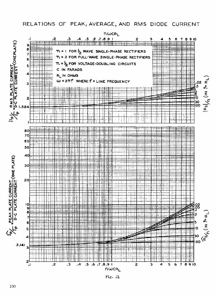
/M.
a
A ND A
; ;g"=:"...--.361.w.°112-.-%==91-----z-2--dis.2F2-121113Jzzer-539was.-xs 2:6=iir ":-...- ------------=
==m=====11. IMI/IINSIM .0111111==M1 1=I=11=IN MIMIMINMEIN =I=== =MEM ''MINIMINIMMIMMIIM I=11=1=
111.01.111MM MM.= 0111=11111111111===1..mm - II II 1 us ..e Le M E B a = = =INIMMIIM===MIN MIMI= IINEMMITIIM.NIMINIIMINIM UMWNONINMIIIIIMINIIMMIIIIINNIMMM MM. " 10
EMBINOIN MEIN IMMO = laill UM=- NN--MM W==ernME==_E=-E.
"mom somemomamon.21 mm.... soma sm. =manimm===12:IIIIMEMINIMMIllaalaMINIMMINIIIMMIIIMBIONla laaMaa nada flia :MI a MI I= Ma Ill Nel==aNall laallIME NIEMEN MillgMan MUM lag. -NM= MOM 10...-- -
101111118Vajc........e.W11_,.../..".........:;%607 istl'%1117....6/8.-""M === e:MULEMII I Brialir..............................wNw
ill at=___,P-....-- =sommem...MOMPARIP
IINIMMI IIIIIIMIIMMMEM'MEMMEMENUMMINN111.111111IMI MINIM= =111111 MIMI 1.111111111M11 MIEMMIIIIIMEM 1111111111111111111111111111
MIIIIMPli
am sonwommulmemsmmi.-...-.....r_-;-...... ...m-_---imin=.arimmi___ arlijuni iljffigR=Eriiiii,----.........minmmiamenuemaimmUM Nis pm ...momm---....!_=--....monnimunis
iiiiiiii ilm=miumsummimMiniiiiiinifiN &TIMES sinkiiiiiMIghl Mini ME III ..
IIIIIIIMMII IN Limmummmuns. iiimisimimmim.
=eaMMEOEMEEf=1== Ma= MOMSIN Ir=1:= NIE =NE nomNam =32.6
ONE MN= MOM MI Mil MYmersionmfflommommumum.mum ME= MOM= EMI MIME..... =
-
"NUMM=EIRE-T-11=E=MFAMM=IMEN-g." 2.41=:; nra nal6TWEREMMIREPMF-111NEErafiljaMM =211MMEMME.SMEE==========
6 O0 INEWLIIELOr::"MBEI°311104EullinEEEEP.s1=3EMEMITIMMEWMOON NM= =MI MIMI MU MIN
Wan Nan NISI WE1 Mr=ME I EIS
UNNIMIIIMMNIIMINEmm Emmet WINN WWI IMO =NMI=Ma
50
40===EE.3=7.- aaaratigm=Emal-r-LISEIMEIB9:ials. zmunam: marimmemi.
wlmmmm..
IMMO...Hu_RI mum§n Min OMNI
MIE=MIIMMOIIIIM nmimam=1,--B faritrireera. "1bn:re.==E=Nonscs2=-2--111
mummos
MINEmsE
=Mn =Mai NOM NM- --=====_MI orm win mesa mem /IMMOM=M1== IWO WEN ORM MUM 11111111111111Mallall= MENEM NM MOW MN INNN MI NMI 1111111111111 INN=MEM Ora riiiillitl MN IN 11111111MI
Nom
MEMNON KIM NM =MNM Amu 11/11111111111111N M MN MIME MN
=61ELMER:11111511.fflaiiiii"-matell
= MEM II 1.11911111NEU so
"LatarnIn.... NM MEE= MU
1==1.4= OWE
o rgesum.....ordiumpromumullNI
MEIN
MINIMMOI I
EEEE=BIANIEHEMMEN IIIIIIIIII 11111 IN_ .11N
_ i ami1111111111111111111111111MPOWN MINIM I 11 MI 1111111111111LIIM IIIIInummffloammismerm
Mill MN MN MEMO al
,,z, IMIMIIIIIIIIIIIIIIMMI MINIM M MIMIMMWIMIIIIIIIIIIMMEN IIIIIM111111111111111re9 EgnnittirgiNii:::%triiriinNINN: ;1 111 : :". : : E : ' it t wlE =. M. 10: M. W ..sue N. N. : :7_1 Z4-..9..ii:361.r-gm-: --- -.- . - - -6 MENEILEffinglingraNiLEBEELcliis__NunMaiMffiM3 -vm-- MONH=MRIF-21._.s'7 5....1 s=1113:19246'sue'-wa.MMEEM....--;.a-reaefili:Ma =1111 s6 mmunamem.K.......EN1 ounssmsraBiREMBEN- MN:mm:1:- =MEMM-Vg....mamati" ... ....m...rap Tararnalimmmiansamm :Pr, we.WO_ __1".".'. -IMMIIMIllanlaaa MB=
1.111 Err- -- -.: ...,.." la I IN u r......./. _wonME ----admilm5 ..mm Immo..." " "-!- =um Mai SakaalaMaN ,r....7,-...MINIIIMINIMIIIIIIMENIIIIIIMIIIIMIIMIBUOINIII IMMO SIM IIIMI I II IIIII M NMI
momiimmilms swop Ems M MEM Wm um mu I=11M1110111111111111111111111111111111111111111111111pr 1111111111111U1 MI= lima NM NI II MU =IIMI===M MIME M IWO I IN lllll N EMS MOM MEI NM won= _....:1:1--e-go moms.......... ll MN IBM MI! MEM BEM mNINA inn ion IIMM E 1111010"--".................. am one
_,wes...opilliiin.--EhrrlisraingiRk=WOE EiNSWEEFIE1111212HEILOMir ...
.....-- _,.
.......0mmoon2 csaintindiallirdina a ME a ME EffirEMBEEMINI3.141 -'3 E
me""mffaCE"'""."1:11:1311INWMEn..1111_1ffigiF IniNI MINIM KM@ MEMEL" illeEINNIIINIMMEMININIONI
..:E..m..........m.w..... .. ..N.- .......MEMMEMEN Bral 1.118 MU gm
monmum rjj I II IMIII Ma EIVIMENITI
MIMI 1111111111111110111111111M1111 MP INN ENNIO IDA 101112=Ellarel==101111111111
MMEN EMMEN WM IINI I MI biMIMI MIMI= NINO= NIII INN E NM 11111=111111111111111111MIIIIMIIIIIIIINIIIIIIIIIIIIIIMUMA...11 MU MIMI= 11111111111111111NNE1111111 III
.005
.2.1
2
5
10
Q:
C30 Cw100 <cr-
:
L
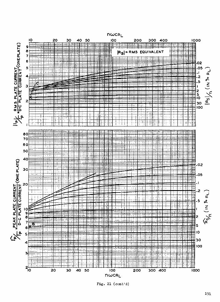
I
' =.......=r,....=..........=.' ........................--7= i=---2..72m51---.1 ----.. ----::-.:-=-3- 5E1E13wra r.6sE a s s E -=- .9711 6 2 21 ali "-: - : :
fai-7.-=----"":22.-..-...:...a.....n-ar.h...::::i;"-=== -- 7-7 ''r'21°''----'.7:22=1::..-21:----11.3441rnAli
..."11111 117'.01111.11 Erirg=a rYMailiE:BEFIE iii: :: 11=======MIM MOON ......::::.,==m2 on=== ....2. 1 _N mums mom mu ..... mmmomolmany mu a. ...._.,,-T..' ......,11.111180 MM. pmpiftlMMI:1"."'"1121111.n"" ==:2:209NwLM iMMMMM Mal MM. 11 OM ME 1=== CIMMMMM1 MM.. =WRY MM7,..:: .17, :1; ..."...."'. Likni."." -------r-n =I & IIII:====mmim'''mwsmna 1= I= ="12==0"4:::-...:=rwrionammmumulimmEn ''' B gra salaam ..... NEM NMI IMO IIIII N== WMa IMIIIIIIN II Mar! .7-7..... 1111111111Aff WIMIMEO 11111131111111M 1111111 IIINIIIIM 1 WIN UM Mil =IMMINIMIIMI IIIIIIMINIIIM INIIION _.,.,,,,egg- MINIM NINO 118111011 NM NilMMOIIIIMMIN IMMIONIMEM SUMMONS= MEMOIR, MANN NNW NM INN INN IMPOPINIPM === ==..., =mom.= EMMEN =NES NOW NMI MN NilIMENIMMUI MEN= Mg.= NOM NMI NEEMM MU MN MN MMINNII...11Min MUM =MN SIMI .......-- ----IWO= IIIIIIIINU MN= moo um nen mu nen ....._=-...=mmo i.=.--;-.111§au mom 1.= We ineawn=MOM= = NENE MEM MINI 111111111
111111M=11111111111111MIE MONISM ION "I:; MU 111111111111111110.1.-"-- WEI MION111111.1111111111111111111 MIN MUMINIM=MEM ums...!-- Hoi IN n....--z.z.-...mo -iluorm.----- -- -ii--...... mem IMnaiad nig ..r..::. Ni ---Numisi inn MU IN mon mum um ensmies nu==.-.---- ----m-:---.7:-ram-=:;ant =-.."'"'=:..............«=m1.,==suiflimmim mommom- ... ;Nigen.:;. --.".."-t= Wen 97". 7..-:. siiii ''.."'".
MM..' NEM ..... -.mai .. -... 1 p Min ...-_=,_......-._......,..--_,...-_,.--- _....-___aa=rivir..,..,....,--,3,...........--.... ... - -em;;;;!=;;;;mcm....=_,....F.7-1.,,--_:---_==-F.T=Fea:="...ii............... ..-aorm'''iz..:.,==...........?..=2:211M === '""Women rale="0Manli!--"g''''''-...*.r.-r-...m."''' wommINEMEMEMENS 11% E,___............-----,..........ammil-- -ft-- z ---A..:.7.4=___ --1..2W__=!!".___._.......05016...rm".."6";r1281___"ge_p_-7 -ilk!' "Inie---ionsiTia-"--. "aaWiiiiiiiiiiiinimiargalWOMilii.,-----...:=, =grom,. mom szur,=.......mlowl 11111NWMMIIMINME NEM =NM PIM NNW MOOS 1111111 1101111 MON nu.......___=--__-.-_ ,,,,__=rtsmorin. mum gm gni ithsiliceWegariaThlinuMIMILTAWAIMI=TulMairsiiiP'.--=.1..= rZill.... =mow mow M. din iiiii Baum ENEMINIMISIZI=== EMI= Mail El WI 1 I 1 I 1 I 1 1siommemonimmENIIIINIMMIONIMINIIIIII IMO NM INN MINIM 111111111110 immili iiiiimMini nisi 1.1111111111111111111111111.111MINIE Mimimom a= mareuri ra wilayrmon arzerrodosolaragararmrin
1 - MMwmari Mi. &MI EMI EN Mn NM red raj .arrara= ummommo.........rairdmoIMMIIIINIMMINIM IMIII1I1M11111.111
111 .1M 11I M111.M111111E
NfflMN NIMMII MN
IiMlIILIEIBMIIIIIIII11111101111111 NM11111MENU 1111111111111=MINN
E
muumMmmmMNMM MWMMME1 E
INI
=.°1UM:M:=6"2E=........2".....ftxtV.IIIMM11= i' M=EN=BEMMENP..........-.......- - ....7==.. la M=..11._____ .. ___=----1----IramME -----5.-m-contwora wo-EMM.....=":11BEffilni.-----....--== .....---="-:=EUI == -NN-m1=21:12NININ:
kftE.:Erj=,:=1,Mne...MME a.." 1=
M =1 a a 22.1 r : =MI ME BE .7. ==== 1.3 =I 1 . omm==.....-31ELI,=mnMMMN =mor-com.v.-oulmonso--z...-----e.ramEEME-Mow..=orNMNNNN..........022..monsp.===aw.r.uum=======malms isimpi .......= MI
1111111.11MIN MallIMINEMO Mall MIN MEM NOMUJIMBIS NOM IMIIIIVIIIIINIMINIMMMMEN MEMMIE INN MOM OM MI ElEsa="Eipiri=ESSFAMT: E.,.........c__:_,___-_-_,Fisolemilimimisagromni=1=M Me.s= -Au.- --r. 1:1- -...- -.............-..-...... ---. mid- ---- - ntr. mulm: tor. all
M.W.'''''Ur."" M'''''''''ann=11111=12111=111IIrsernr=a;ii,
---.=.---5--assillEUMIEMMESIMEN===MN.
eon mmmgo-lima =In a Mel 4 ini.- 11;... -'. . ' 1 MBN ME =WEEP 8111i
L'!".-"1"."1". ommonmsia1677NN.EEumms in..77.0.2.111MEN692 0 :- =
pimp a WI Ilia.iiii ir Nilmw...eigm-dilira...m...-..====n-iindwm....= Mil....u. 11 =MO MOM MOO UM MIsx-.....--.0-m-6-Nmeiririat-----mawraimo=ommorn...Ai" 01115._?...--. mom mem WM mum A
ma N
werriola limn 111111111111111M11111111111111MW1111111111111MEMINMIN WM 111111MMIIMI im
...0.:7 um ......__Em.....araimem...................... .........milik-ummiiiiirsaummoram.:A24 _damiiiimmalialallehro_____ .....................................rardorimilimmilli ill
...1 _:.....wimoimm EMI NEIEMI ME BM EMI NEMIIIIIIMIIIIIIIMINN NM MIWIE-44P-f-,-EM= =L. -1"Z giii 6-0-1-7-miiiiii Ai iiii1=--- ----- am= EmoviMPOUVE 11Poff= =MME=FAMEMENIMMEEEMEMMENNEENomm---gam memoromommffiFiz__=_mmoimmA ....W:
NP:=MIEMBEINELMLwa....T.Ems m a6 mEs -.==-=AimmEs m men m es m me tos.-a....---. -amin naissararamains Nam um um= misNa====nMSINCNIOINIIIIINEINENCIIIMINMINMUUCHN
blaNraraNglEMEN.---rENIMMENNINNWMES::M
---.....-...MNN0,,,,,r....,,-.= MOH NM WM ESN 111111110111
EinffifflimMIP21--2---W.E.ffiliffilliennl.....i...;,..........................
.............................,........................MMINNINNUMMIIIMININIMMIMIIIIIIINIMIINIUMMIliallinellikleassmENEINEMMENNEENIEMMENEN-mmaimmpougirdi.mmsnom------War:AM61KPWOLL-LiMNEE EERIE
EIE.RIV.41 BEEEWE:- MEN 11E1111MINI
..... m"sommillarrs ri--=-. -.3=:. romEEFEEEummEir.rmtgl la ,--imilii.......11111111IIIIMEmum11111111 my. =OMEN IN BERM mom= Effie
7060
50
40
30
z
E- 20ZLLI
Cr CrCt
Dt)
41
41( 10-i
0. a98
U7IA6
5
4
z
.02
.05
.2
.5
2
5
10
30100
se
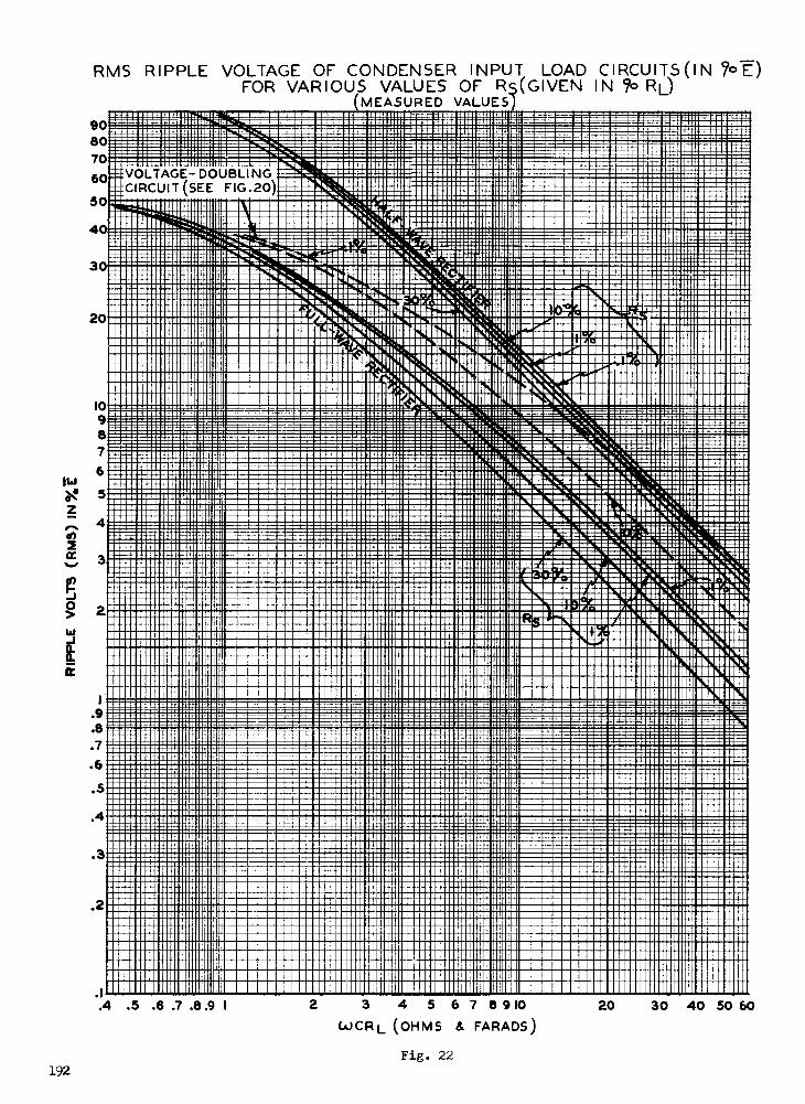
161
z
ICr%me
um I1 MP aA a
-
a D
. _=====.........Ic --=Esas- ....c. 7.1: --- ---...s.-...Mas.eita------ .E11:5 -----
1E12 ===== -- c......
a ----- - szwilitilitinginiiir. - -1!-- ill.5 = Er.=...-,,,--.-= e. ; - me e n.a.......=====ramiaai=spe-man - I: .. a '11= ....: ----- ..... - . 2 1 . =====jammearags-------. NM ....._ ,.. n Manill°=151B32.1ENEESS: ii *. 1 MKS MIMING
... ...
IMAM 111111. aj! -....::la , : M.V .. .. ... .. ..... ..... ..... 1:=22===. 11 '
1=1=Malli ... .....:Ili in n iiimr.mma-manianralmmtommir.ifNM
6 iiiiitin ..IL IM.9111.20:. ..... 1........ ..... .... '1"1.....
..... II ..1..111111111=MIMIIMUI11111OMME M MUUMUU M. In..
20
1098
15.. _ ME MIEME1111111111111EIE EMEMII.4 'L., `IE.. J.111I ins...-.Efgagrs nu1N1 1a -- -.,.. _. .111111=11,11MNINIIIIIIII .411, AIM . 11111011111Eme.
..... ........................ EDI ...... rii;,;,gorr muniniumEnn. . NrInuilikomprilling' 11...: i.... . I:: . "...."%i."%li.i.-- . ...
. ma mono ., 1. -11111=a= EL iii 2 22311111!! 41.::Za2.22-==i-pqs. ''. - 7 1 .11. 110.=1
, Ili andaBye1IM5N.
= . '''' MM.."'" ". Jr"' 4., ..'==ii riagna - .611...1111 CL == =ZVI ... SONra74.1.1sCe4111Z"....."""""nnilaaaaMMMINain "MM. ,.. Man Nana ..... ..... liliiiMaiant/gMl.=. = al::: . .......1
.rIIMIa....111 , , .... la .. 110111=111EIMM.EIMaIMINI ppm ...dismome....o. MEI M....11, t.11101111.11M1011\ N. . = MIIIIM=1MN = 1 ..... IMO ...1111111MOIIIMIN '1111M=MMIM ..IMMIIMIIIIMININI 11 _. M1111111111111111111111- "EMU MINIM . IOU Rill
II1.1 111111111111111. ,3111131111111111 -IMF-. MEI I.113,. 'IlsIMEEL. MII. MI T-1.24 NEL ,II. 0 'Ile. 111111111111 MIMINEEIMMMMIE.L.2
1....11FF,2,11 QOM., s 4::, 1 ..... MU IIIMMESIMMITIMMElm., MTN" dii111
"I ..... 111"1.1MMILIgg '!::::7"11"6- 1,- "wa """.:, Z .... 1111111=Maill'i:i.....:r jai1. 111111111 NNW'..... 1111111111111111111111MMEME OM...M. 'NUMMIOIME4 . 'Mb 11111 ........ IMMMINIM/1111MM pais s ===mousm 01101101111..:911M1 \JIM CIIIII HM10...1111111 INIMIMIMMIIMIIMMIIIINLNIII I simians 1111111MIIIIII
IIIIIIIIIIIIMI111111uninnimmmmommom ENBI"AgIVIII.'111111INIOIIIII:11111111111W P":111111111111101011L. %MN MEINIVIIIIIIIIMIIIIIIIIIES innIMMOMMUIMMIMIlli OMMEIIIIMMENNEMIN,V111:11h MI.,'IliMENninlillith:41:. 0 INNI1 EMMILIGLINIINIE111:111111111N1111011111111
1111111111111111111111111111111111IMMINIMMIMINIMILZonom: mmissoulmomii..1.,,: MINE1111PIRiamassoaasessomommosionmassiiiiiniummiiiimnommEmmosinismiliMihriihzatiiglimomilomito.' ra.wisimuummunnr;:gmmisnimummoulinu1111111111119111111111111MIIIIMINIMMO111111111111 '..?Salhigli!IIMIlliNIM111;1111: viMENIIIIPtiligillillkfill1111111111111111111111111IMMilliliiiliiiiiiiniiilliliMEMiiiiiiiiiiiiiiiilibir4Oligli:Zillifiltinilliffiii.1 ON7riniiiiiiiiiiiniiIiiiiMillifilIMNIIIIIIIIIIIIIIIIIMIIIIIMNIIIIIIIIIIM111111111111111111111111i5lEi:911111112q111111 a\ No1111111111111111111111111111111111111111111111111111111111MMINEiiiiiiiiIMMIIIIMUM10!11:110,911111d111111.10NMMIlliil1111111M11101111111
kiwi :',M. -=-===-...s= e
m .... ..:. ............ --- . a
7
..-A=E-SEr--MSS
.1=1110=1.11=aI I
-c
OnDr
m.N.iM11iE11m/M1M"
mU =.unI.II
a.ElM
a.Nalla.Ma=ni
i==.i==.. i.=.. - 1111
..IIMMMIUMuMiMEMlMMNE:...............scsMseenuNaIM11I===MME
mm:3 a n.a;=====. =. .Manaaaaa OM ....... "."=" =LON... : :..====... ... : IEF:a 7 .17 ...;s r 0==1,..110 Zraft..Cril: 'fa . a,
::::: "51111.1=--='-=' . a.. 1 - lir. AZ.= .1. II NOM 0. .'
MINIUM .11=MEMMMIIMINII IMO =MIMI AMMIIMMMk 1111=1=16 UM.
hummara- -- . .. .. .... I MIMS 111=. e . milui i, IFir.omm. . ...... IIU' Illeir-111 III IIIIMIN IN MM.=MUM MEM . 311MIMIIMIONOIONOIIIIMIIN g ..... UM 1: ..... 0 ...... INIINE IL -A MINIM I., UM
M. -.U. IM=M11. 111
Inn hej IMMINIMIMIIIIMMINIIIMEIIIIIMMIEEN . IM ...... MU ll Mk 1M=MEE 11111/
M==MIEM .1 NM 4. ,, -NON C MI,.11.` 'I ..... %01411. 11iii 11M111111111111MBINIMM if 1111101111111111110 01.14MIN k In ILA: 4. MI 'EMI`
11 MN MEMOMEE . .... no9 -man Tul,
.... III MIME \MIA _AI. ME ..2 1111111 dmillinill=c2012:1L... ,,,.., MIME MSSHI 1-111111111 ImEINIMEM
.101
111111111111.11111111 11111111111 11 NI IN111+0111111111111111111111111111111111011111111111111 11111111111111 L.CLALIIIIIMIIMINIIIIPA11111111.711111111:111111ANIIIIIIIIIII. .4111111..AVIIINEWVIll
MEM MIIIIM IIIII 11111 111111111111111111111111111 NMI 111111111111111111111111 um sesssuensummanumn MAIIIIIIIIII11111111:'AIIMMEIlligl Iiii7111111& . :11 .. INVSIIIIIIIIIIMIMIIIIIIIIIIIIMIIIIIIIIIIIIIMIIIIIIIIIIIIIIIIIIIIIIIIIIIIIIIIMIIIIMIIIIIIIIIIIIIIIIIIIIINIIIIIIIIIIII 111111111111111111111.1111LIZIONIIIIIS:11111011111in11111111111111111111111111111111111111111111111111111111111111111M11111111111111M1111111MINIM11111111111111111M1 IMINI111111111=1111111111111111111671111101111W \gill11111111111111111111111111111111iNMMIIMIMMIMMIIIIIMIUMMIUMMUMUMUMilifil ELNERMINEMEMOIMMIIIMI:111111CiiiVign11111111.111111111111111111111111MINIMMINIIIIIIIIIIIII111111111111111111111111111111111111101111111 MEMIIM111111111111111111111111111110111111hIllhM11.111111111111111111111liffifillE1111111111111111111111111111111111111111111111111111111111nifillfl 1111MEMENNIIII1111111111111111111110iiiiliiii!iiiiiiiiiiiiiiiilliiiiiiiiiiii.niiiiiiiiiiiiiiiiiiiiiiiiiiliiiiiiiiiiiiiiiiiiliMiliiiii 111111111M1111111111111111111111111111iNIIIi1111
I:: es:E1:::dia=-Wa=-= . .1.. wz= ez - r1"."-iiiiIW.--==rtsa==== s ---E--2 -= E;2--__::P sac -PE c: = ===.. r. .. --1111.1111..... ...E=EFX211C1fil M JESS .. .1: .
I . :: . 1 . Hi -.===-AredilailiElini:IEN gar' P- .-....
2Mani
C 1 :o suill
=mai ..... almi m m .....game. ..... !gni:EC:I PanE...'3WMOMME r01221 gEgg
milthm mm;:iiiriroarag== Lai . gg:ICS11111-= g q:
VESEEM.MMIIUMIIIIIp'... g .. U1110111 r"...3281173 it =..54,611 -EL" ..,.................11 . . .-...2::..... .... 7.3ss- is - ...... L. . 2 .. rum-nr.mgeral..m...-.. ... ed..::: istunilidi. ....r.r.znEEN-= .. - ..... II MO .... ran
I .. 1111 . 16119151111:11111 .. IIIIN 6.11,114711111:1112.-.2:-.2::::::::::::___, ....... ....... I
IMMO MEMel
=MI11111111 111111111 IINEWAILN mr111:81111111111.........111mil 11111111EN'AMVE" . 1111111icq!=.-.....E.....zaa--lin ---N.HrtmE=EE474=mosimm = S
11411IP E'EEIMMZE'''''' ' .. -Ni====== -s. NH1 1..
... L!iiiiiiipliEwaRmaElizzlEan ...nr.......Fr raarditrea=rEZ= =in!1
.311 r in: gis---&-:-. Pqm:::=0111BEES6z--- - ...r um m:
111=-0sh-anm.-11 ..... d:11-1..... ...._......
131. I. j....6 . -In ura.nounii &Nur -:moss c: .. In
.. 1".1111.:=ME.M.:11 1.....5...1..1........"'ImimUnil EINZa"'m ..mourn
.. i ini daniSTABIIIILysemialiadininin ........ la'..::: ... m..... ............1.............. ... 1111111111MMIIIMION1111111111111MIIINI EIMMIMEEMIIIIMMEMEENEEIMNUNN IIIIIIIIIIIIIIIIIIIIMEINEN1111111111111111111111111MISOMIIMIHMIIMI BUM 111E111111RM IMIIIII MINIMIIIMIIIIMIIIIIIIIIMENIIIIIIIIII 111111111111111111 Milli
IIIIIIIIIIIIIIIIIIIIIIMMIZIIIIIIIIIIIIIIIIIMIIIIIIIIIIIIIIIIIIMMIUMUMIIIIIIIIIIIIIIIIMMUM111111811111IIIIImmumpummiNINIMMOIMMIIIIIIIIIIIIIIIIIIIIIIMIII111111111111111111111111H MNIIIIIMMEMENUMIIPIUNIMMIMMUIMI1111111111111M11111111111111111111111111111111111111111111111111111111111111111i11111111111110111111N11 IIIIIIIIMIlinsolpiusimmiumnimiliiim
IIIIIIIIIIIIIIIUUIIIMIMIIIMMIIIMIIIIIIMIIIMIINIIIMIIIMIIIIIIIIIIIIIMIIMIIMIIMIMIMIIIIIIIIIMIIIIUIIIIPIIIPIIIIIIIIIIIIIIII
""." " MIENIMI laan1111111.
. MOB 11111 Mk MM."' '7.1.%V=ZZ":'"" " " . Lm'a :- .....111111.1181= ..
... Is NMI'S MUM,.NM-NOMMIL1111.11111E I
..... 11II MEM lk MIN 1 . `OHMInkIMM1 ..nIIS.'S MIE
..... eiminghoiNEILMMi.,011M..... cnommiousm.., IMINL'k MIME' .51. I.'1
ORM=
..
6
5
4
3
.9
.8
.7
.6
.5
.4
.2
.1.4 .5 .8 .7 .8.9 I
N EMO .
2 3 4 5 6 7 8 910
LOCR L (OHMS & FARADS)20 30 40 50 60
192Fig. 22
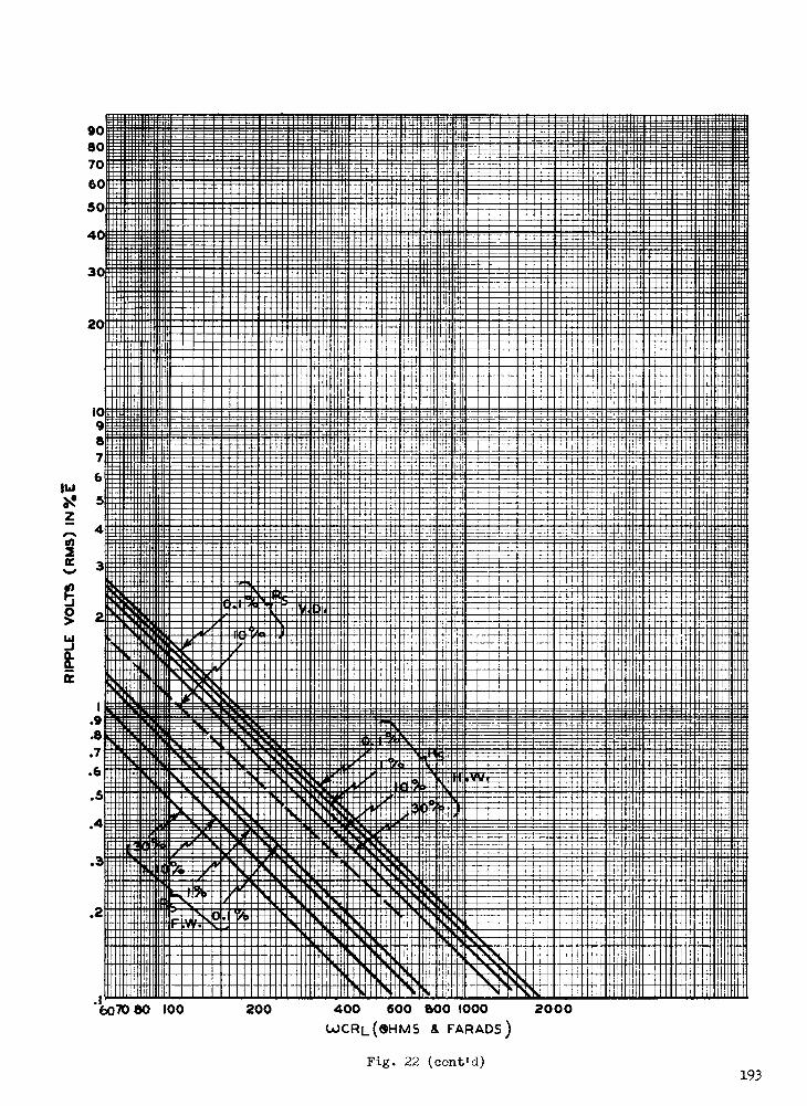
O
z
Q
90807060
50
4
30
2
109a7
6
5
4
3
.9
.8
.7
.6
.5
.4
.3
.2
.16070 80 100
==run : ntunz--=-
lllll
1.4ffititigriniatimp-mmEs...assuralEcS1 as==-===3EratniqelaZ: =21.5 -----31 rniq iglea...-ZEBE.24:2 mainnia ran g ---
===.
1 ...... lllll liM1411=1=IMBIM===14111111
.. In4Mmal
II EMMEN= MMI lllllllll nth um mmimm1111 x11 1111111111111
111 =MINIM rani wanzramenr.warmrrim..1::::::Mhlint :a1 irms..Imu i in....0.... - muumuu
-- 9.9116:0:112. 0....nuag...-........... . ma .. iffirdi-.nuinommmma ...----a=morming._a.- ..... ----L. 1 1
IS WM IIIMIMIIII RmyroMIMMRIIMINIRIBINUOINNUNEN:IMIMI ..... EMEM IMIIIIIIIIMBEI .......morn nramemumu stramozra:::::::aramum ..... BMW
....m. ,..,... .:::...... .mime nii.lareal.,..,==-.=_ -4-32,----,..:. a :221611 il ....=11IMIMMI... 1:=:::::Iiiilez=---3993E2thu:-,--0--k===.02-M-- ....dhil-oz:::: Inn ...........----,,,........
M:Milh.9111:91%:: 6.nrin 7111 II rel::::11......lhardl6% O W MO Off 11::::111=....====
H.I...... IC qi .... g.mmi ....- ird IIII=SE. REA . giravaunie ii
IN q 1.. IIIIII11== . MI NINIU 11 arlarea212:21MOI MEM ..mum. siIMO 'IMMENSE Minn= 11711MUHEIROMII MIMI ir MIIMMEN=111111.1....... III
MMM111111111111111111 MI11111
II Mil IIIIIIIIII IIMMONOMMII UM ....... IIIII =MEM= II =RUSE !mall NEM Ili 181 =MMEIm.1111111MINIIIIIINIMMIIII1111111111111111 IIIII 1111 ......... 11111111111=1MM MN . IIM BAUM infill11111111 1.41.11111221LIER MUNRO COI IIIIIIMI "'" IIIIIIIIII ..... um
1 lllllllllll w111111111111.1111111111111 RIII PIPIIIIIIHNUI MIIIIIIRIIMIN MO l INNERSMU 1141 WU UM = MM ME N.M. OROMMIUMM MU WU 11111111111EIMMOIRIMMINEIMMEMEMME111111111UMU1111111111111MUISMUI111111111111111111011111111ifiemmummmmonsmmminumulln11111111111111111MIMMIEMEMMIIIMMIIMIMMIIIIIMIMMIMEN mm11111 NEM1111111111111111111111111.1111WW11111ifillIMMIIIIIIMIUNIIIIiIn1111111111111111MIMIMINIMIIIMMIMIMMUMMIIIIIIIIMUMms iirommun IIMMIIIIMIIMMMOMMIIIIIImIllunlaMMIIIIIIIInuIll111111111111111111111111MIIIMEMINIMMUSeumnrimumnEi EIMILIZIIIIIIMIIIIIIIMEINIMMIIIIIIIMIiiiiiiiiiilirrinilligniiiiiiLifiliminnumnuin mimumommumumilunummommumunamiumnm11111111111MIMMMIMMIMMIIIIMM1111111MIMIPIMMI MIIIIIIMMEMMISIIIIIMINIM1111111111111101111M11111NM 111111111111111MMIMMMIIIIMMOMMIIIIHMIMMINIMIIMIIMIM MMIMMINI!MLIIIIIIIIIMMIJMIJEJIMMIR1111111111ni:Eff::::::Ei-q-MEEE:-- ll" 2r. l SIMMINMEENNENNIOMMEINAggfflEEITHENtrSIME-N.To.1 4..r...
41- llll -- -1:1=-=li ll 7.61.atrilMIMMIMMERDIMME-&Z41:11idllizliglu_i..u.--::::: llllll ;:.:1:::: -01 Mri-kileaVEILMMEItiMiffiffirikEridge;g:f:-.....
esrairaMMIALam====sramm-:g .2.-.1=_ -1....r.lum:
s.
: E:--i
N .........---__ lll ......n.... u-- MIMMEM=ESE--31--MarraziEtellustio:
I
1
I ..,iiir...-....... ..::::::imithimEgaffliinurvor-======="40115:112:2--rairamk..=111111MINI
111=1111==11M----Incalra....mumumn ff,..21..mor....11INN
11==INIMMINIM M11111114111.11 WM 4 MM BMW/MA in l 4
IMP lllllll 11111111 MOM=IM1 lllll minimummn nil mom ll pmll Olir"EMEIMILMIEMai so 11111111111=
mum __moan IMIIINI ' AMID 111111111N1111 MMUS 11111111111111111111 MINIM!
MIR IMIIIMINIMM ER ar IIMMINIII NUM MIMI NM NMIMS1_111111IN NEESE VENN IM II
IIM MI NIMEINNIIINMMENINM M
l OEM LIMNsmellEMIIM IIRIIIIIIIIIMP=1111MR1 maimmumme lllll IMO 11111111111111 MNleas::::::::::: llll a .:::ti iiIiiiiiireis warp Ewa! g=w..-Egm=wgrp.mi 1...m. nas:=_====== -srang...ussunnum- - ........--- .. .......m.-.2wp.:- lllllOS 111 ll: lllllllll
76"1"1:194-111.-1=99PridruFS.2zr-53.-151.-11LkiigeuroMmul2611Phirliklui:ummns..... lllllsammiliiiiiir I urainnicism Fern ismix====k1E.T.p.'.. rdarairdalliroliMilia ' llllllimmim PIT fluI. .T.E.:213,... MI MEMEM EWE 11 ON14 MEESE ME Ind Clii 11113011EASEE1::::: EMU: U OIL 0121111111111, lll
I. %.,I.'", INMANNININIMMIEWAI =MU diallINIIIIIMINENUUR rin11. .., llllllll 11111memmumnribwi L'umademon nualun mem NAmi. %,,k,111:. 001 11111 1111 IIIIIIIIIIIIMIIIIM l MM.: s...am.serro ran tem MUM II
ZEZZLI'''''' ...,..AIIIMIIIIIIMMV"Emi=. l N I. tiLIIIINSIMM MONISM IN MN NNIIRAMITiriblIMUSINTUMM101111111111FUNIU11 PM IMI11111111111INIRRIUMIRIEMIR MIIIIIIII ME MUM IN lllll URI
MO 101: 0111111 ==l111 MI a llll IIMMEMINMMI 11111111ifillIM=MMMMEMMEIMUINIIIIIIII MEMMIONNI111111111010%!.;.1 momirrAmarnwel91111111111111111111111111M11111111M11111111 INIUMINIMINIONIMMIIIIIIIIIIMMIIIIIIHMUNIMMI111111 glligligglIIIII111M1101:Villi INIMMIlp/illiNINIOMMIMIIIMIUMIIII1111111111111111mg
,31111111:11.70:1111MOIMIMMIGMINIMI11151111111111111111111111=m1111M1 EN=11111111111111111111111111111111111111111111111111111N11111111611 111111111111III11V1111111a:111;11 VIAMIIIIIIMIWAIMIMMIIIIIIIIIIMIIMOMMIIIIMMIIIMMumM11111111111111MMIIIMIMMOMMIIIIIIIIMMUUNIMIIIIIIIMulli
11111111:1111111111; 11ZONID19.41MiiiIMMI1111111111EMMIIHIMM1MIMHOMMEMMIMMINM 111MNIMM11101M1111111Mill1111lb.111111 Ob. 0..4011191111111111111111111M111111111111 NM PIIMIIIIIIIIMM11101111111111111111 IIMINIIIM1110111M11111i Niiii111111:1.11111ok-;e111111111111111111111111111MIIIMMIN IMIiMMIIIIIIMMIMIMMIIMMUNIMMMIIMIIIIIMMIIMIIIIIIIIIIM1'0111111 Illi 'no.\ NR1111111111111111111M1111111PRIII IplIiipmqminummunununummumoRipupoppul:-. --eal.7,--.4:=:== -nlin-------r--E.EEHE.iiiiiigiggiamm_mtwilminhicilimilli Ellinaluntal
- :2 "'rd.- ruratriTHEIKEN=3-2-rlFfflialgrireliAreliffi PIT-.:-.:Iwsz-9,!2-6...a. :111-m==-EF.:=5.:--°-=-,,--9=-:,,--,,--.2.,E=M,,:- dh.,!"- AIF:llllll --- .124.4k4,12901.401=METITIFLE irlingin3129211413.1.-430iiii6:::I IL 1::::.=7.7:," llllll --"IMM: ...SLIMMlin1::.';,11.1:-'37:EarIM ... ...inEM1131FALIE mu
lllll II, REM.. = M=1 iMI. MEL "1. lllll lll AMMO HI .nMni....ITIPOSZE aD. ll / Ani POI in eSt14111111=E...raza::::::11.6411...1%,,:r us mu
IL TilhOla2-.....-- l :::-.2-" ll 70,""'"--- -10,5115111, llllll il ,.,M1,MMILNIMMIONIMMI 1 "4 l WV 1 ....fa ZNINIMIIIIWINFINVENTEZMMM ...KM EV maim LEL Jai um111b1;11E'nEESEE-wjiilirdpaltill:111MINIVIIII
, It MIMIOMM.`110 l !BMWS MN, oil NEMO EENIMMIIMIN1110111MENININE1111 lEnramouninn....libuipimn11111111111111111h. NW MINE,M 'IL I. vI , 4 EMENOIMION llllll NI II '1111INNIENNINENNINIIII
HI 1101=M1 1MM \ 'II.II M. 'IMMISOMM/0
*: :101111111111S il 'Ale rlfl II 11111111O lll min MIIIHNIIIMISIMINERIIIIINN 111 I MI umI.; .....h ...........18i.....:Mini:ITMOULIV="iIIIBMUMMEMMISSIMMLIMIMMIIII"" 111111111111111111
1 l HMO NIIIIIIIII 1121
I:.:: I ll 1::::..:12 25ff::1g: ]!...71.4311171; ie "FIPIPIPM dial 7".jijErardrE-m-111111111111M lei NE':e=: -S1MU lig-. .. l . l mmx.m ..... ...
:11,192 llllllll ... l F.1===2.7'.11.12... V. Of al. di /,.1.111Mik 0.111411M Val
11N =ill'aTBENEEETardswism:
......Min 1201'mgREFIEffillibiliniir"111:11:10:1,, Zi="673112q167''oaaaramonr"
., le ..... II1V01111
no-niiiir-1:-.E.-musui-3-szramuffludrii-Implreauss,maltokinup.....r.n.:=1-No.mat.suluz..1...r..nwira
.lllllllll Mil ILI MYEMEN IMMIN A.1.. - .... I ......... M=IM=MEIMM Eli 5 .1115En.11.: 151.1... L..IN MOM:ft 'I knomu iimmommmmismannim I n
mum lllll piiiii miN11,7111111111111K 'A. lII II NM MI . TIIIIIII 11
I ME III; INimumn. Edllll u II.111.
MIb 1111 a1M1v:101Ri mmioNnornmoriiiiiiiii. . . . Rimsom=wininiumemm mi ' 1 Illiriunt.s.,.1.um....
'HMI llllll 11111111k .UNOW=MININ l 1:41111.111101 MEHL 1141.:11111:1111:11t 101111111mmomommoss asMad an u ggi. llnunimumu
u t....71.:1 l 1 ll Illeou....mossaKom.. Or lok "Iti witemmin mom 11111115111111111111111 gigininuol HIWM IMIMII IIII mirrrmou.'icim'Alimmommouin.1111111~11111811114111..11k mit,101%111111111111111111111111111M 5111111111111 IHIMISIMMOMMU11111111111111111111111.111MmiALImomlmmommmilmoilImk11111i ll .1 ll 11211 MI 1111.104. MINIM WU nu iiimplionsuritu nil111111111111ifinli MM........1111.1.11"1"ir"11111111 qh:41MU1111.... inininglingrill Mil gliiir Offilill11111111111MIMIUMIMIMIIIMIIMIIMMIMIMIUMIV111116:4 IM.:1111111 .9110167111111111111111 11111111111111111 IIIIIIMIIIIIMM WI MIMI1111111111111101111 M11111111111111111111111111.111111111111:111111k1111111N111111111 0110001111111111111111111111111111111111111111111MUM1111111111111111MNIIIIIImmumnim somosomminnumunhounizuh. Tim ipilinAmmosilimmommumniromieumminurimmumpum immmmumnimamlnin nunoluoli ..10111111 0 WIINEMIIIII111111111111111 1011 numnimm IIlull 11111IMIIffilffinNiniiIIMMINUIIMIOilli. NOM iNIMOWOCIIMMENThifiumnimmiumminnhummpmfinumm11111111111111111111111111i1111111111111111111 1101111: IMO IIINICIZESNIIMMUMNIMIMIIIIIMUMIIMINIIIIIIII
200 400 600 BOO 1000LOCRL (OHMS & FARADS
2000
Fig. 22 (contid)193
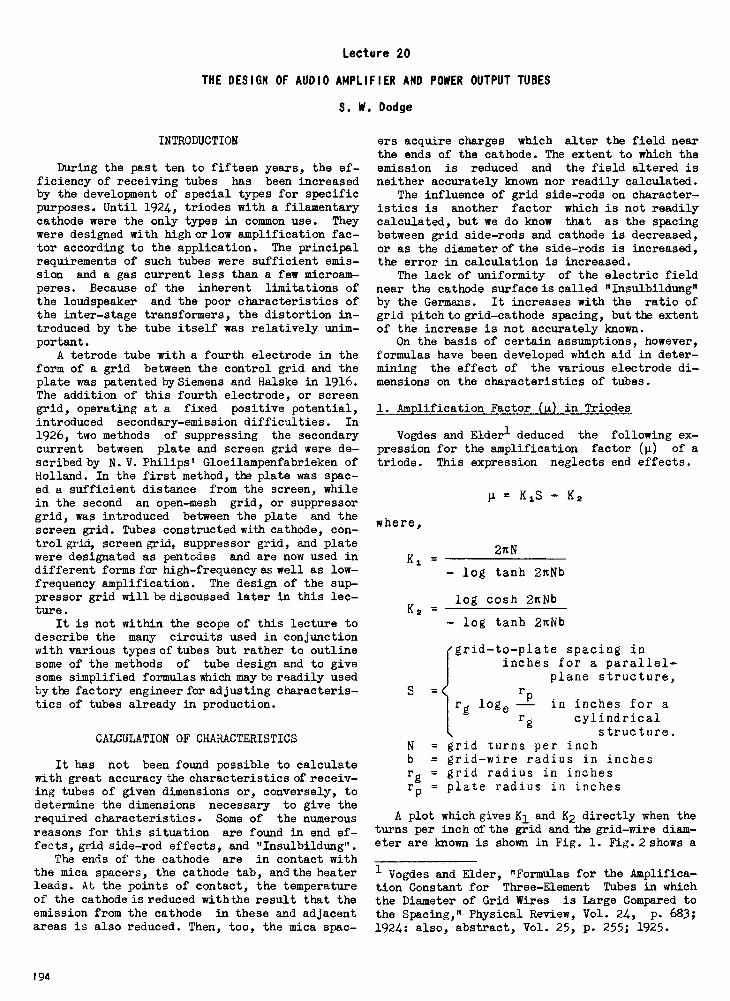
Lecture 20
THE DESIGN OF AUDIO AMPLIFIER AND POWER OUTPUT TUBES
S. W. Dodge
INTRODUCTION
During the past ten to fifteen years, the ef-ficiency of receiving tubes has been increasedby the development of special types for specificpurposes. Until 1924, triodes with a filamentarycathode were the only types in common use. Theywere designed with high or low amplification fac-tor according to the application. The principalrequirements of such tubes were sufficient emis-sion and a gas current less than a few microam-peres. Because of the inherent limitations ofthe loudspeaker and the poor characteristics ofthe inter -stage transformers, the distortion in-troduced by the tube itself was relatively unim-portant.
A tetrode tube with a fourth electrode in theform of a grid between the control grid and theplate was patented by Siemens and Halske in 1916.The addition of this fourth electrode, or screengrid, operating at a fixed positive potential,introduced secondary -emission difficulties. In1926, two methods of suppressing the secondarycurrent between plate and screen grid were de-scribed by N. V. Philips' Gloeilampenfabrieken ofHolland. In the first method, the plate was spac-ed a sufficient distance from the screen, whilein the second an open -mesh grid, or suppressorgrid, was introduced between the plate and thescreen grid. Tubes constructed with cathode, con-trol grid, screen grid, suppressor grid, and platewere designated as pentodes and are now used indifferent forms for high -frequency as well as low -
frequency amplification. The design of the sup-pressor grid will be discussed later in this lec-ture.
It is not within the scope of this lecture todescribe the many circuits used in conjunctionwith various types of tubes but rather to outlinesome of the methods of tube design and to givesome simplified formulas which maybe readily usedby the factory engineer for adjusting characteris-tics of tubes already in production.
CALCULATION OF CHARACTERISTICS
It has not been found possible to calculatewith great accuracy the characteristics of receiv-ing tubes of given dimensions or, conversely, todetermine the dimensions necessary to give therequired characteristics. Some of the numerousreasons for this situation are found in end ef-fects, grid side -rod effects, and "Insulbildung".
The ends of the cathode are in contact withthe mica spacers, the cathode tab, and the heaterleads. At the points of contact, the temperatureof the cathode is reduced with the result that theemission from the cathode in these and adjacentareas is also reduced. Then, too, the mica spac-
ers acquire charges which alter the field nearthe ends of the cathode. The extent to which theemission is reduced and the field altered isneither accurately known nor readily calculated.
The influence of grid side -rods on character-istics is another factor which is not readilycalculated, but we do know that as the spacingbetween grid side -rods and cathode is decreased,or as the diameter of the side -rods is increased,the error in calculation is increased.
The lack of uniformity of the electric fieldnear the cathode surface is called "Insulbildung"by the Germans. It increases with the ratio ofgrid pitch to grid -cathode spacing, but the extentof the increase is not accurately known.
On the basis of certain assumptions, however,formulas have been developed which aid in deter-mining the effect of the various electrode di-mensions on the characteristics of tubes.
1. Amplification Factor (11) in Triodes
Vogdes and Elderl deduced the following ex-pression for the amplification factor (4) of atriode. This expression neglects end effects.
where,
-
K2
S
µ= KyS ''' K2
2nN
- log tanh 2nNb
log cosh 2nNb
- log tanh 2nNb
grid -to -plate spacing ininches for a parallel -
plane structure,rP
rg loge in inches for a
cylindricalstructure.
N = grid turns per inchb = grid -wire radius in inchesrg = grid radius in inchesr = plate radius in inches
A plot which gives K1 and K2 directly when theturns per inch of the grid and the grid -wire diam-eter are known is shown in Fig. 1. Fig. 2 shows a
1 Vogdes and Elder, "Formulas for the Amplifica-tion Constant for Three -Element Tubes in whichthe Diameter of Grid Wires is Large Compared tothe Spacing," Physical Review, Vol. 24, p. 683;1924: also, abstract, Vol. 25, p. 255; 1925.
194
Dodge: The Design of Audio Amplifier and Power Output Tubes
plot which gives S for a cylindrical structuredirectly when the grid diameter and the plate di-ameter are known.
For small changes in µ, such as would be neededfor the adjustment of characteristics of an exist-ing tube, the approximate formula is
4 = K3 N2 d Swhere,
K3 = a constantN = grid turns per inchd = grid -wire diameterS = grid -to -plate spacing
It is not necessary to determine or know K. Toraise µby 10 per cent, for example, merely in-crease d or S by 10 per cent, or N by 5 per cent.
The error introduced by the use of this approx-imate formula is quite small. It increases witha decrease in the turns per inch. For a changein µ of 10 per cent, the erraris2.4 per cent at20 turns per inch and drops rapidly to 0.4 percent at 40 turns per inch.
2. Plate Current (Ib) and Transconductance (gm)in Triodes, Tetrodes, and Pentodes
The equation for the plate current of an idealparallel -plane triode is
Ib = 2.33 x 10
where,
-6 A
dgx'
KbEc + --
4
+ 5
1 + +
14 dgp
µ 3 µdgk_
A = cathode areadgk = grid -to -cathode spacing
Ec = bias applied to grid
Eb = plate voltage
4 ==
dgp =
2
amplification factorcontact potential difference
in volts betweencathode and grid
grid -to -plate spacing
This equation for plate current of a triode ap-plies also to parallel -plane tetrodes and pentodeswhen certain of the terms are defined as indicatedbelow.
Ib =
Eb =
4 =
dgp =
plate current + screen current
screen voltage
amplification factor fromcontrol grid to screen grid
control -grid toscreen -grid spacing
For all heater -cathode types of tubes, the folapproximate formulas are convenient for
making small adjustments in the plate current andtransconductance of existing tubes.
Ib
gm -
K4
= Ec --dgk 4
1.5 K4 / EbEc + --
4dgk
) 2
3
2+
where K4 is a constant and the other terms are thesame as given above. Combining these two equa-tions, we have
gm
Ib
1.5
EcEb
4
For the filament -type tubes, the following equa-tions give greater accuracy.
Ib
gm
K5
dgk
Eh
(Ec+ 54)
2 K5 lbEc + -
dgk 4
2
where K5 is a constant.By inspection, it can be readily seen that the
error introduced by the use of the approximateformulas decreases with an increase in µ and witha decrease in the ratio dgp/dk.
With µ and gm known, the plate resistance rpis readily found from the relation rpgm = g.
3. Power output and Distortion
Class A Operation -- The most important char-acteristics of power output tubes are the poweroutput and distortion. For class A operation,they may be calculated from the plate -voltage vsplate -current family using the grid biases asindicated in Fig. 3. Ec = E is the normal op-erating bias. The undistorted power output is
U.P.O. =2
I') R
where
and
II =4
IM&X - Imin + ( II - 12 )]
Rp = Load Resistance
Emaz
max - min
195
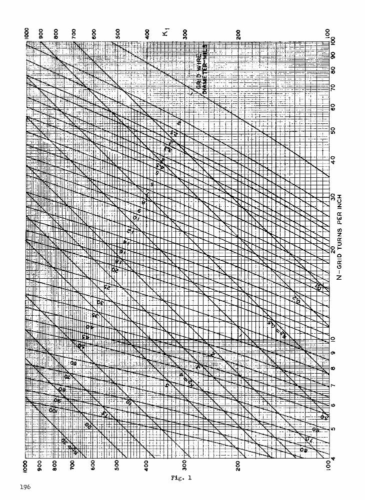
1
-4trij ErlasalsWEEE&E -11===
orgw-13= - =1"filtEENF_.
Wai:t.
111141/41bItia. lq
a
-5 "TM
ird=
7.2:=
NE - - Asa'oai
,N
a. - *whi-m- _U. . MOM_um---minimoram--.ptin_ -21 -941";:mgAnteiNFAI"' WAINEIN mn_IVICis =am
b;siiiii -.moo -. h.... ........ ink....1. --= r, ..
.42.,kaing,..b...4&.',, . - - mina_ tilmak- kbASZ"-marmei- E =EN- EIN Db. imib.1- 'nil -
10,Rmi -mong...0_446,N,432.c..-znarzr.---aamorarsora---,--EMg.., ... .. MO ..". 11101111111.11111111n111 MEW! MIM===11.11MI
1 4 MN' 46020MOWN. la. jilibMLIbilall'ibabria,7111111bil b.. riat===iirai-----Z2=1,2...II-Zia:AM 4 . rainniumbromr.,lots.
aa.nt...,i" .1111\01/11 ,111F111111MIN1111 MM 10 MM MIMMIMIM
bi2111111==1.-MM M. mammimmim
min hirini. is.- woo mressi Emosum wiiiimalimmtw mil-gunnmmumoniumwomminmiaa Millbtah
1 briers.tmommihwommatiawib...imiie.. ..:.Nammilmmoriomm====ism...saiimililift...istiarmeoit -rms mhzoininimmiewolistaouumuumminuiommetim
werlimiri vitiromminIquirannOmiloraiNiamorianusirmarkralehm'-' ,,. IN 141.% ,,,,Nah, mom Mb- IRMOIMII01...41hg_ Nal . :11.11.10=111.011111111.101.1.1.111111.11.11.1.1.:smii11.111INNIMIllata21.111VIMINKTO .1101. 1104.11.11110.111.111.0111111111111.1111111111111.1.11011.!?Jahinli...lail41111 1110.1.1.1101.10.111MISIMMIZAMOSIMICS.,E1111.1351.11iMMINNEIMMOIRIIMIN111111110
leillilliallIZOIMEZ.11111MOMINK:MMORIM \MINIM -11111NOMENIINg\MINII.NIMMIIIIIIIIIIINIIIIIIIm horn. slum Immmitha.mionsiggiunriournowiramorgemmowiinsowsoumsommumum
iinahliii. I ilfr114110111110.1111111111NISMINsirnir.111MM01.111M1391M101111111112111211111Mw911111110IMIIIIIIIIIII
ISHINWINIEIMMilainiraninillanilaellinge214111111WailltralliMEINNUMNREINEIIM CM _&_wifilL41110911111111112111111MINSIIIIMIMN.11611fflONIIIIIIIMMENO..11110di :MN miiiiihilio..._ llmz.. wilsuciamituntrisiismatisimiiIIIIIMR21111111111011011111W1M11111M011111111111h1114kit, UNIIIMIIMMIIIIIIMMIIIMaillfillailIMIMI0110111100110.111.11111BCRINENN,,:lillinnuiliiiii:MlunkiunilaiMIUMES1011134111:PMEMSENIMEINIIINZAINMEINSomMEIOCIIIIN
MI6 IiiiVIMINduliiiiinikIMMISHIMMUMEMIIIIIIVAIIIISIMINS11161.1111111116511112111.411110.4.MIliiiifelt. Iffillillhnift P!11111ilIllhsaglliIIIIICCIIIIINIUISSEP.IIIIIVIIIIMS1911lZLIIIMEVIIIII\P.111!16:Mll.i.MIIIMMiliiirMIIIMMIlhaV1111111117911121111211111111111111111M11161:1111311111131111131E311111111ElibleMil!1111101r111111111iiiM111111111101;:9114111MR111113211\11111111SEESIMEMIEBeINENEMES1111110111MailliiiMMIMIGENIM1116:101111:::§111101113 CCONFOLIMIRSTACCFRETIMMENIIMIIIMINIMENNIIIMMIIIIMNICROmMenardliintilNIMNIMEMimui thignumopinummo -iriligrirger"-"Numboanic--emougi -N190--1-qo1111111 mo whibilitmmik, 1111:2411111:250311MMEMIIIMMISC.AMMINUZI Mail 1110134111., aliffin11111MLIEMISCH """ffik '"LV:PIANIIIM
--isk 1h11 illmoim r-isimew--limmiiiimpintimillitioi",_ NIEL 1117.inhaik i i MIIIIS
EIMMUNIMPOI 9411rulk.111101411111121411. Ifling4:11110111:11110.34111MBrepall -- 'NA mudigonikieb.summismambommacJimb....i.;N... ingumnomenimmmosimmumumamingiarosemammasi
.... iipishiri WhigriiiiimuirninuRommtwasommommiNingengreuili;....h. illIttu.. 11/4 r ina..._ 141111111111611111111MINI1601111111 WW2._ NE- SO
ligq IMPIIIIriiiiirillihnlipliliorniNIUMMORIMUINMELIONMESSEMUINIMMICIMISSal11011111101114M11111111411 1 .fillliallilliaMillarginlanlIBEIMEMMIBESUINEMINii3.1 I itigrati..,. Clgagrilii-M1.P.102-.VN§Cr-Fg0040ffimmEsmilm=-_-,....-4m.
Egalitraggint;a160.:§01.00.111.410BENNEWALlankaME-=-' Z 3 WEN 74: Miliab IL -44111. --22h- killqaxaggagr--31,34.. 10
au umluvar- MONSM110.123061- -- 'NE_ irmi7E-IrfirtmEIii.I:
es:.
:1,T
TEME&Z"nig& ElibahLUL.
roarirel IIMEEE3b. ....11.: -'--E.rimil?EL =M.._ ,_.4_ L-1:11agtageljjb=-:.siErAreg==
MNmown. irardraingliiihk -;11 -461-0AIEN-"%P.IMIC"..P.RThir.-4......En MIN
' =21ith\ -IngEINEEMOLIBMW
: ....i'llan =mmu.""5"it, =1.1E1 m...x .N:Ion: weniras 4. Iriliekoli....... mizmn-m =Go...AM....- . mwm ...._1111\11LtIMINI11=1=g1M ,
4211 1Pi`274%.5111 NignPeigEhiangmh.1111-=:-.narag.L.._
....1=11
Feribtig66451
s:rom
ltikr-ti lZigaiN.rM--i-b6..
Ig"Naalkig*Ize e...zik-rEae
r...rnniriqgIUUMbunr*bii MEMA.MZElMFRINNMMMh'
II am0ft. EZmagm Ii. -
1 11r11ltIAIIIlMpIFIIIIEN NElIP ElaffIMIp1SitiniliRSA
M1I1I I0I1ibli1 UaM erMnnibOM l ILIMMMEBea9raftft

iTIP.ORRIERM wiriE -zanyEIPANNUMIMIUMMIrrralrer
ikIdrhisamitE
Ina.........uminiqi..... . .50-1:h. 1 - .wring ' ipmaiii.:..:::;1121.: somiludil.6 ..,.....noir qip
1111111INII II I Iimam= lignisiAlpo 0........p.mi.1..m.v."....... --I.:-or -
IN10.11biffiliiindin:1111111111UMIIMIlla
IME1111110ifigurrn IIIIMINEFMXIII . mr.e.....m.m....iimmmunimpuipm 1111linfuti no p 1.11,-;?..minumumhimm. mom. IIMOIMM11111MIMI IIIIIIIEIMIIIM III
lommiummnifininquinimoilimiiiiiimilin um ousiummum mum=moinummmi. IIMIBEEmiiiiiiiirimingi nig
union iiialiiiimpliiiip II IIa III Illu MUM=Moulin IlaM1111111111.. IMMT11,1IIIIIIIIIIIIIIIIPIHINIIIIMI II II II II WI IIIMMINEM
ummitinumlliormillqu Pladiiiiii inummommMIIHIMONliggri IImii ,..
.._ 11111W1 MEM - 1111111=11111131111111161111.. I 1$I 111_11111U Aill11111111111111
ill 1 Ir-i111111111111111111 OMM MilME11111111101
11111191h1M111111111111110n1111111111VUIINA-
IMM..01111101111101p11111M1111111114AMOIRIMMIN
ii:PliitPlilliggniMililrnillinfillAnillirill =NM11111i190111101:111111211111MMINIIM111111111111uthiiiminopuminplpiniii! NIIIMPo1umem
irivilii Is ingrinunegung muggsgs par, 9ns rinimMEMEono . i t.. h. Ih. I h. as 111114104111qMpirighilIMMI11111111111111111,19911MEIMMIMINIEffla immm HEENEmi iib. hi. ih. 6. b. lh.IIIIIIIaIMIMII IN II II MINI NM MO==IMNiellLmm.immiellinallirlinnEME
gosialiimentimiplinptalquelpislimmolomerni.:Erammummonsmanwispouglitaluiwnitraman.he..u111111111:61::111UMEIIIIIIIIII:::
11101111MIERSESEMISSIMIUMIIIIIIIIIIIIIIIIIINEMEMINIIMMENIN:dilgik.lorigiiigiriralpiti:OgiiininfailliniIIIMOOMMICEESEliri"Ight iiIF 4111161441qIiiiIMMIllnilniiiiiiiiuh. b.! tka. .1.! ih.40.4 N.A. . lb. M
agiSMENNiniablintellS11311131111111111 riuminlirals::::.11,%limilpirwkidgipmimizullimookramosaimumsnamieminANINamotiiiunnomulhoihoubmitaniumuitalsenessobsmumwomilimmommasamonmmuumTemillivingmailirilliquirmagitistamizassamommouninnamommuii!iil!tok,,P111itidhlaiiihmu wlithltulbizokoliisbicsizenceasimmismuimuunism
milliionigozig..; -IL -mgg.hm-igramkgRa-2gFi..--muNE-"T.----01 vr-s-t1411J7A.161102.1MhoikurolarinzwiN*2-amM 111100w.-_-
comercmq --Km-Alm -4403-8 '" 'a Nlif,414 'INNEE1--ighttiothrialhh,...-- Nia*.__,.....-.1 riorati takk..-matAk-k_htitab, kb. EA
...4 WOE -1141442%114111h__ 4114.1100114 '114%. -711E/WINCIVIIIIMOWEIBII=MPlitra kilttt. bleghaihist. b... Illts.. Staggr.12-1411§-kilgngling=719c, 701.1111b18,.._ hit..-44kh -Provir===z-ectiarent rigor--st--imhampiri! 1--slino-r. -.0.1--sh.----2-0=1-u_,..=-..... hzbamoiat.. Es.==.. -4
,rquuotlhopkn..!!Lrdu.IS!gdihig-WikbbSkV9NC:Zkl.IRLTO4E'':irim-Irirr---R -Nv__411%1LNe446M.;.11168111131; !, 41 1144- keliA .10.:Ifilliksh141.04,-Ath_ARAtiA4Vikh6TiVag-"44411liP3 h
hN11414 itimP.Wqh.. Leh". ik. .-i-Tx_db.:atm.:, inv._ ...! --- ...,.mgarnozntariwtl-Z:74.7-41-wl=t4"\"6366-711417.6::41":13/4:":1MLm--m-;4t,guirMb4343%.4\3
- '. "lk. - .4 turn_ quir jut_ fti. j_ ...ii, vs %mama%kinigliiriiltrifslipudiettIlilframitiblieristaquilialliokb- Blexibem614460..nik.414,6.0..r.tit,.,....
I. 11.;iiit lihniblinlibblibraiirlitrikkw S m_Imusia.: malsia.umou suriassmaimi.. al.igsi mir.sh:w11 rimiisaaaa-maosig.iim6swimareh.me Fa II. .qmome.shmpoomwa.-.11 mum. N.
inanamisommummosinsonsionsm_111
MBE
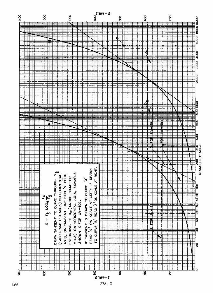
8E-_=----===IN ==w=m= S =-=-Em===-gE===g=g=
w-7,1 ======-======= =s- E=========--
oRmammaa--- sam:B.m-=rm22:dm
L-- mOMMLTAM.IMAMMOMMMERM=== mom1020:2 monmmmmg.mem =========mmm. MMOROMMUNCOMBumOmme == rJ ====== mom ====== mum=======m===m_ -===mmmmm-.-= ====mm..===m=mmm....==mi2===m==m..==. 6=== --
mEm = SEE=Ma
a-
lommilimmimimmummimmmmummins
O MMOMMOMMEMO MMISMIMMIMMiii=-I=7==-E -:=== ===.zaf;g536===E3====BEEMES51111111§11111=====
--.-...11====m.- =
!m......====-s..= ==SE:E2111ilinn.WIMM1
'--*MaIMM, ..0 M
M -...MMra: . MMEME .-,-,
11====MOIMOMMM.
RIMINIilirrammummommEmaimemMimmEMMENam gim:fts.._ MMMMEN aMM7.11 EMMCMIMM= MMMMMMMM BMWa AUMMINIMM ===== nallIMMUNO=Mammammama.-"Mmalle ==== Mina IMMIll
MAMMM .MMM = ..i'.= - "4M:===r- ===z -E=
-...=BEESMIES=55===E--== = -=.:-=ggsg--=
w" S-MESIEwaES==== -----=
'
------=E==== ---- - -=
== ===-== --- -.,...-m
=....1.
M==..m.m.i=MMOMEmm M :ME b.,IMO .OMM R--
0 .. m Wiwi'....: .. .. . ...161.. m..mm ........ 0 0. ===== ..MMENI"-=',.., === m..m// //74/74 IIIIIIIIONNOMMISII.6..immal1: === .4.1mmimm.mm.m im=Mumma IMIMMEMMEMMEMMEMEMEMMIMMMIWAIAMUMMEMEHMMUM IIIMMINIMMINIMMEMMEMMEMMEM&mgMEN3MMEMMIMIUMmMINUMMM IMEMMEMMEMMEEMEMMEMMEMMUMMENWEMEMMEMEM . MEMMEMEMMEMMEMEMEMENMEMMUUMMEMMNSUMMEMMEMO .
. . .. .
MEMMIMMO . IIIIIIIIIIIIIIIIIIIIIIIINglinaliniMUM MEMMIMMOMMEMMIMMUMMEMMOHMOidimilmildiMEM= IMUMINIMMOMMIMINIMMINNINNIMMUMMUMM1B EEEE=E= .
E=E-_ . , MIIIIIMiln=g2=ffi===E="====-SE=-ME=E- . .IffieS1111011:----= ="SE=E-- M -ME=
====== . =-=ESmlil-- - =- ---= .==............- -=== "..-..--=g==="= Ilasad==== r======
========EMS ===M===11= ...=
FammEnnialas...---
. --mongim-===.-.............,im- -..- - mmumm.com---.-----m002.0111'
:.------ mmmm--------------.--- ----. 31.
'1174:=
---
.........
misimmommismommi1MMEMEMEMEMMIN
±
ME
.-==--:-.-
Al
1....MM22
Ea
WM
=E=--
anirEIMIIMIIIMMIMMIMI
mommismommminiummumIMMEMMEMOMMININUMEMOMMMIMMENEMMEMMEMENMEMIMMEMMUMMEMEMEMEMMEMEMEMMEMMINIMMEMMEMMEWNMEMIMMEMMEMIMIMMEMEMOMMEMMEMEMMIMEMEMMIMMOMMEMMEMMEMMOMOOMMOMMEMlEmEMEMEMMOMMOMMEMEMMEEMmEMEMMEMEMIUMMMOMMEMMOMMUMMUMIMMMEMMIMMEMMIMMIMMEMMIIMIMMIMMUMMUMMINIMMOMMOMMCNIMIMEIIMMIMMIMMIIIIMMIMMIMIENFIMONIIMONOMMIMMOMMIMMMOMMUMEMM--E
nagiblIMOMMIllballaMBIEIL:NmmIMMEMIIIIMIIIIIIIIIIIIINIIIIIIIV41112:1=1:111
ENE-==mms
mommumm.ammulhaummommi.nommlhimmummommmimmminimmommummummmumummum
ManNEEIENMENAIEME=
m m ...
== E=54:==ts-- = = -===0=1==EMESSE=B====E=
=N=======F::,===I: '""" --
.. . 1=====MME =BEM I"============= ..
. .iiiiiiiiiiiiiillillial=
=amp!mai:
=WS=.
-....m. m-- ..1..-............
MOM= WM MOM IMMaamMallall . a aaMOOMMMUMMMaaMMMOMMV IMO=
11 a 111211E563EM====11
-==-=-==!----- 3==i-======r===m=====- g=========amm-= =-====- am-_... .......----=.- ,--=mu= . aMEOSSESE900 ..mn---naga-----mmagm-------
' imm=mainaill==ziETEPESSMEEMBEREEa
2: . . -.Imo .... ___.:mmigm.= .6...d ram-- .. c . . - ...
'''''Binimmornim........ . =IF 10010.01..:.... .. .. ... ..... ,..
... ............... ........m...........................m....mu ....................................u.mm.................mmu..........mmiummmrnmumornm.........mamIIIMMOMMEMIONMENMEMOMMINImill MMEMMEMEMMOMMEMMINIMEIMMOMMIDIMMEMEMMINIMMEMMMIIMMEMNIMMOMEMOMMEMEMINM MEMEMMERIMMINIMMEMMIMME EMMEHMEMIMMEMEMMIMMili MOMMEM=MIEEMOOUMWIMMON MMOMMEIMMumMIEMEMOMOMMO EMEMMEMIMMEM MOMMOUMOMMEMMEIMMMIIMMUMMOOMMOOMMOOMOMMINIMMIM IMMO MOMMIMMIIIMMIN IIMMIHIMINIMMIMMOMI
MEMMHOMMEMEMIMMOMO
-
====[.."MMIIIIMMMIMMaMMI
Ogt
198
0 OO
0ID
O O
80
8O
8
8
8"m=1.2
cw
8w2
0
8
0
7
0
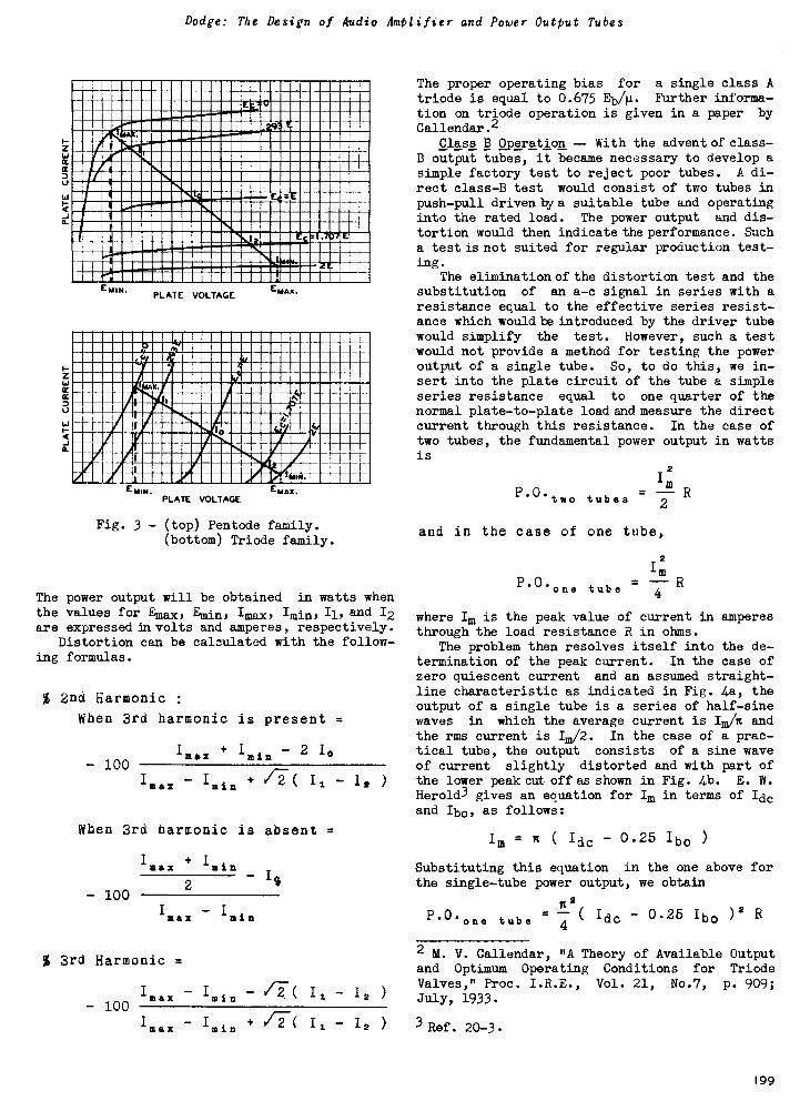
Dodge: The Design of Audio Amplifier and Power Output Tubes
et
a.
E114114.
E4L1
493
E
11M--
PLATE VOLTAGE
1
c
E
E MAX.
11111111h..41 A
4111:4EHMInipummasisvmmomm Egminummmummummumpimmummormumm
rum Ammommormum
IIIIrmalpullumurallil
AI
N.PLATE VOLTAGE
Euta.
Fig. 3 - (top) Pentode family.(bottom) Triode family.
The power output will be obtained in watts whenthe values for Emax, Emin, Imax, Irvin, Il, and 12are expressed in volts and amperes, respectively.
Distortion can be calculated with the follow-ing formulas.
% 2nd Harmonic
When 3rd harmonic is present =
- 100Isax + Imin - 2 I°
I... I.i.
When 3rd harmonic is absent =
- 100
IMax + Imin
2Is
IMax Imin
% 3rd Harmonic =
100I 111 X
'sin /-27(
-
- )
'max - 'min + fir( I2 - 12 )
The proper operating bias for a single class Atriode is equal to 0.675 Eb/µ. Further informa-tion on triode operation is given in a paper byCallendar.2
Class B Operation -- With the advent of class -B output tubes, it became necessary to develop asimple factory test to reject poor tubes. A di-rect class -B test would consist of two tubes inpush-pull driven bya suitable tube and operatinginto the rated load. The power output and dis-tortion would then indicate the performance. Sucha testis not suited for regular production test-ing.
The elimination of the distortion test and thesubstitution of an a -c signal in series with aresistance equal to the effective series resist-ance which would be introduced by the driver tubewould simplify the test. However, such a testwould not provide a method for testing the poweroutput of a single tube. So, to do this, we in-sert into the plate circuit of the tube a simpleseries resistance equal to one quarter of thenormal plate -to -plate load and measure the directcurrent through this resistance. In the case oftwo tubes, the fundamental power output in wattsis
2Iry
P'" two tubes = 2 R
and in the case of one tube,
2
IsP."one tube = R4
where 'in is the peak value of current in amperesthrough the load resistance R in ohms.
The problem then resolves itself into the de-termination of the peak current. In the case ofzero quiescent current and an assumed straight-line characteristic as indicated in Fig. 4a, theoutput of a single tube is a series of half -sinewaves in which the average current is Im/n andthe rms current is Im/2. In the case of a prac-tical tube, the output consists of a sine waveof current slightly distorted and with part ofthe lower peak cut off as shown in Fig. 4b. E. W.
Herold3 gives an equation for Im in terms of Idcand Ibo, as follows:
Iry = n ( Idc 0.25 Ibo )
Substituting this equation in the one above forthe single -tube power output, we obtain
2
1312"one tube = 4 (Idc - 0.25 Ibo )2
2 M. V. Callendar, "A Theory of Available Outputand Optimum Operating Conditions for TriodeValves," Proc. I.R.E., Vol. 21, No.7, p. 909;July, 1933.
3 Ref. 20-3.
199
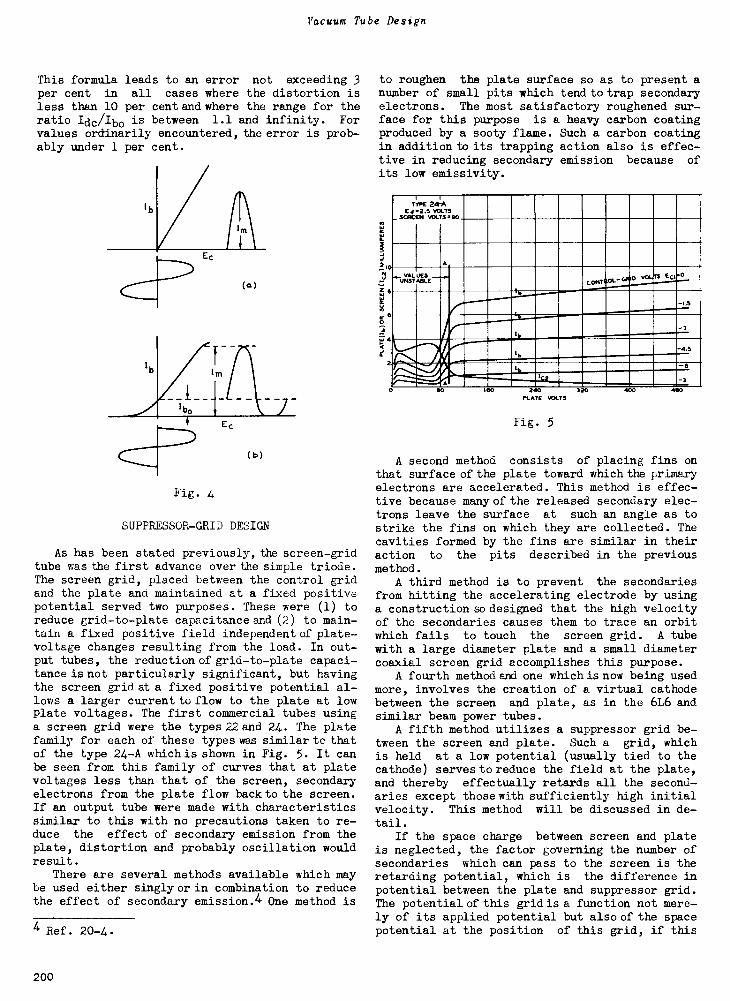
Vacuum Tube Design
This formula leads to an error not exceeding 3per cent in all cases where the distortion isless than 10 per cent and where the range for theratio Idc/Ibo is between 1.1 and infinity. Forvalues ordinarily encountered, the error is prob-ably under 1 per cent.
Fig. 4
SUPPRESSOR -GRID DESIGN
As has been stated previously, the screen -gridtube was the first advance over the simple triode.The screen grid, placed between the control gridand the plate and maintained at a fixed positivepotential served two purposes. These were (1) toreduce grid -to -plate capacitance and (2) to main-tain a fixed positive field independent of plate -voltage changes resulting from the load. In out-put tubes, the reduction of grid -to -plate capaci-tance is not particularly significant, but havingthe screen grid at a fixed positive potential al-lows a larger current to flow to the plate at lowplate voltages. The first commercial tubes usinga screen grid were the types 22 and 24. The platefamily for each of these types was similar to thatof the type 24-A which is shown in Fig. 5. It canbe seen from this family of curves that at platevoltages less than that of the screen, secondaryelectrons from the plate flow back to the screen.If an output tube were made with characteristicssimilar to this with no precautions taken to re-duce the effect of secondary emission from theplate, distortion and probably oscillation wouldresult.
There are several methods available which maybe used either singly or in combination to reducethe effect of secondary emission.4 One method is
4 Ref. 20-4.
to roughen the plate surface so as to present anumber of small pits which tend to trap secondaryelectrons. The most satisfactory roughened sur-face for this purpose is a heavy carbon coatingproduced by a sooty flame. Such a carbon coatingin addition to its trapping action also is effec-tive in reducing secondary emission because of
its low emissivity.
A
10
N
0
4
2
ITYPE
Ea,_ SCREEN
24A= 2 .5 VOLTS
VOLTS .110
A
..._,A145(S ,,,,D vOL/TS EC' "
NI --1.5
1111
1.."." -3lb
lb -4.5
r---lb -6
-A
IC, -3BO 160 240 320
PLATE VOLTS
Fig. 5
460
A second method consists of placing fins onthat surface of the plate toward which the primaryelectrons are accelerated. This method is effec-tive because many of the released secondary elec-trons leave the surface at such an angle as tostrike the fins on which they are collected. Thecavities formed by the fins are similar in theiraction to the pits described in the previousmethod.
A third method is to prevent the secondariesfrom hitting the accelerating electrode by usinga construction so designed that the high velocityof the secondaries causes them to trace an orbitwhich fails to touch the screen grid. A tubewith a large diameter plate and a small diametercoaxial screen grid accomplishes this purpose.
A fourth method and one which is now being usedmore, involves the creation of a virtual cathodebetween the screen and plate, as in the 6L6 andsimilar beam power tubes.
A fifth method utilizes a suppressor grid be-tween the screen and plate. Such a grid, whichis held at a low potential (usually tied to thecathode) serves to reduce the field at the plate,and thereby effectually retards all the second-aries except those with sufficiently high initialvelocity. This method will be discussed in de-tail.
If the space charge between screen and plateis neglected, the factor governing the number ofsecondaries which can pass to the screen is theretarding potential, which is the difference inpotential between the plate and suppressor grid.The potential of this grid is a function not mere-ly of its applied potential but also of the spacepotential at the position of this grid, if this
200
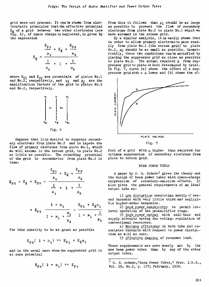
Dodge: The Design of Audio Amplifier and Power Output Tubes
grid were not present. It can be shown from elec-trostatic principles that the effective potentialE of a grid between two other electrodes (seeFig. 6), if space charge is neglected, is given bythe expression
Eg =
Epi EP+ E +
µ1g /12
1
111
where Epl and E-2 are potentials of-rand No.2, respectively, and µ1 andamplification factors of the grid toand No.2, respectively.
Pt
PI Pz
P2
Ep1 Eg EP2
Fig. 6
plates No.1112 are theplates No.1
Suppose that itis desired to suppress second-ary electrons from plate No.2 and to impede theflow of primary electrons from plate No.1, whichwe will assume is the screen grid, to plate No.2as little as possible. The retarding potentialof the grid to secondaries from plate No.2 isthen:
E - E = EP2g P2
== EP2
P1+ Eg +
EP2
P2
1 + E + E µP1 g 1
1 + µ1 +-1
1'12
For this quantity to be as great as possible
Ep2( 1 + Pi) Epi
and in the usual case when the suppressor grid isat zero potential
EP2( 1 + >> Ep1
From this it follows that al should be as largeas possible to prevent the flow of secondaryelectrons from plate No.2 to plate No.1 which wehave assumed is the screen grid.
By a similar analysis, itis easily shown thatin order to allow primary electrons to pass read-ily from plate No.1 (the screen grid) to plateNo.2, µ2 should be as small as possible. Geomet-rically, these two conditions can -be satisfied byplacing the suppressor grid as close as possibleto plate No.2. The actual required µ from sup-pressor grid to plate is best determined by trial.In Fig. 7, curve (a) shows the effect of a sup-pressor grid with a µ lower and (b) shows the ef-
P LAT E VOLTAGE
Fig. 7
feet of a grid with µ higher than required foroptimum suppression of secondary electrons fromplate to screen grid.
BEAM POWER TUBES
A paper by 0. H. Schade5 gives the theory andthe design of beam power tubes with space -chargesuppression of secondary -emission effects. It
also gives the general requirements of an idealoutput tube as:
1) Low distortion consisting mostly of see -end harmonic with very little third and negligi-ble higher -order harmonics.
2) Good_power_sensitivik to permit low-level operation of the preamplifier stage.
3) High_power_output with self -bias andsupply circuits having the voltage regulation ofconventional receivers.
4) Maximum efficiency in both tube and as-sociated circuits with respect to power dissipa-tion as well as cost.
5) Effective damping of resonant load.
These requirements are more nearly met by the
new beam power tubes than by any of the otheroutput tubes.
5 O. H. Schade,"Beam Power Tubes," Proc. I.R.E.,Vol. 26, No.2, p. 137; February, 1938.
201
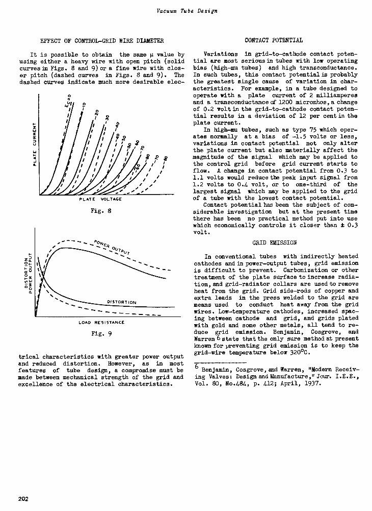
Vacuum Tube Design
EFFECT OF CONTROL -GRID WIRE DIAMETER
It is possible to obtain the same µ value byusing either a heavy wire with open pitch (solidcurves in Figs. 8 and 9) or a fine wire with clos-er pitch (dashed curves in Figs. 8 and 9). Thedashed curves indicate much more desirable elec-
I -
Z DoaI._E0NWCC
00.
PLATE VOLTAGE
Fig. 8
POw"wu/ wr
DISTORTION
---LOAD RESISTANCE
Fig. 9
trical characteristics with greater power outputand reduced distortion. However, as in mostfeatures of tube design, a compromise must bemade between mechanical strength of the grid andexcellence of the electrical characteristics.
CONTACT POTENTIAL
Variations in grid -to -cathode contact poten-tial are most serious in tubes with low operatingbias (high -mu tubes) and high transconductance.In such tubes, this contact potential is probablythe greatest single cause of variation in char-acteristics. For example, in a tube designed tooperate with a plate current of 2 milliamperesand a transconductance of 1200 micromhos,a changeof 0.2 volt in the grid -to -cathode contact poten-tial results in a deviation of 12 per cent in theplate current.
In high -mu tubes, such as type 75 which oper-ates normally at a bias of -1.5 volts or less,variations in contact potential not only alterthe plate current but also materially affect themagnitude of the signal which may be applied tothe control grid before grid current starts toflow. A change in contact potential from 0.3 to1.1 volts would reduce the peak input signal from1.2 volts to 0.4 volt, or to one-third of the
largest signal which may be applied to the gridof a tube with the lowest contact potential.
Contact potential has been the subject of con-siderable investigation but at the present timethere has been no practical method put into usewhich economically controls it closer than ± 0.3volt.
GRID EMISSION
In conventional tubes with indirectly heatedcathodes and in power -output tubes, grid emissionis difficult to prevent. Carbonization or othertreatment of the plate surface to increase radia-tion, and grid -radiator collars are used to removeheat from the grid. Grid side -rods of copper andextra leads in the press welded to the grid aremeans used to conduct heat away from the gridwires. Low -temperature cathodes, increased spac-ing between cathode and grid, and grids platedwith gold and some other metals, all tend to re-duce grid emission. Benjamin, Cosgrove, andWarren 6 state that the only sure method at presentknown for preventing grid emission is to keep thegrid -wire temperature below 320°C.
6 Benjamin, Cosgrove, and Warren, "Modern Receiv-ing Valves: Design and Manufacture," Jour. I.E.E.,Vol. 80, No.484, p. 412; April, 1937.
202
Lecture 21
THE DESIGN OF RADIO -FREQUENCY AMPLIFIER TUBES
T. J. Henry
INTRODUCTION
For good receiver performance, it is de-sirable that r -f and i-f amplifier tubes havehigh transconductance, low signal grid -to -platecapacitance, high plate resistance, and low r -fdistortion. For economic reasons, we are alsointerested in low heater power, low cathode cur-rent, small tube size, and ease of tube manu-facture. At very high frequencies, low inputand output capacitances and low transit -timeloading are also essential. The relative im-portance of these various factors depends onparticular circuit requirements and an engineer-ing compromise must be made among them to de-termine a satisfactory design.
In this lecture we will discuss briefly sev-eral of the above characteristics and indicateapproximate methods of obtaining them. Exact de-sign formulas are, in general, not available andso the designer must proceed by the cut -and -trymethod using his past experience and the avail-able formulas to tell him what alterations tomake in order to obtain the desired character-istics.
The desired characteristics are most nearlyobtained in the r -f pentode.1 This type can bemade with high transconductance, high plate re-sistance, low grid -plate capacitance, and lowr -f distortion. The tetrode can also be made tomeet prescribed characteristics provided theplate voltage is not permitted to swing belowthe screen -grid voltage into the region wheresecondary electrons flow from plate to screengrid. When the plate voltage of the tetrode ishigher than the screen potential, secondaryelectrons flow from the screen grid to the plate.The magnitude of this secondary -emission currentvaries with plate voltage and reduces the plateresistance below that which would obtain if nosecondary emission occurred. Due to differencesin the surface conditions of screen grids, thereare wide variations in screen -grid current be-tween tubes and in individual tubes during life.These variations make it impractical to use ser-ies screen -grid resistors with tetrodes in setdesign. In the case of pentodes, however, thesevariations do not exist, and so the use of seriesscreen -grid resistors is practical. Since thepentode has higher plate resistance and more uni-form screen current than the tetrode and can beoperated with equal screen and plate voltages, itis practically the only type used for r -f workin the modern receiver.
1 E. W. Ritter, "The Radio -Frequency Pentode: ANew Use of the Suppressor Grid," Electronics,pp. 10-11; January, 1932.
TRANSCONDUCTANCE
The equation for plate current in an idealparallel -plane triode is
Ib = GEb Ec e
1 4 b1 + - --p, 3 p,a..
2.
where,Ib = plate current (when Ec is negative)Eb = plate voltageEc = applied grid bias
= internal grid bias= amplification factor (grid to plate)
a = distance between grid and cathode incen-timeters
b = distance between grid and plate in centi-meters
- 2.33 x 10⁻⁶ x cathode area in sc cm
(cathode -to -grid distance)2
and
G
. 2.33 x 10⁻⁶A
a2
Designating 1 +1+[ 4 b
as a ,p, 3 µa
differentiating with respect to Ec, we have
ib = _13 + Ec + ejla/ II.
dIb 3GdEe 6m µ c
It can be seen from the above formulas thatthe gm can be made larger by decreasing thecathode -to -grid distance, or by increasing thecathode area, or the effective voltage. A de-crease of n % in a increases gm to [100/(100-0)2%.An increase of n % in the cathode area increasesgm by n %. In both cases the Ib increases lin-early with gm. An increase of n in effectivevoltage increases gm to (100 + 01/2% and II), to(100 + n)3/2 ?. Increasing the effective volt-age is the least efficient method of the three.The supply voltages and cathode wattage (andarea) are limited by the set requirements.
The value chosen for the amplification factormay be determined by a number of considerations.
203
Vacuum Tube Design
It is usually made fairly high (about 20) in r -f the following approximate formulas are usuallytubes in order to obtain a high ratio of gm/Ib, satisfactory:since
±112.- 31
Ib 2 Eb
A
+ Ec+ E
However, the choice may also depend on the cut-off voltage desired or on the magnitude of gmrequired.
The grid -to -cathode distance can be decreased
only to a certain point as determined by diffi-culty of manufacture and lack of uniformity. Theusual practice in ordinary receiving tubes hav-ing a grid length of approximately one inch is touse a grid -to -cathode distance of from .008" to.015", but spacing less than .010" increases themounting difficulties considerably. In specialtypes, such as the acorn tube and 1851 for useat very high frequencies, this spacing is re-duced to .005" or less to obtain high gm and todecrease transit -time loading. In these types,the characteristics of the tubes begin to departconsiderably from the 3/2 -power relation owingto the non -uniformity of the potential along thecathode and possibly to the effect of the posi-tion of the virtual cathode.
In tube design223 it is desirable to keepthe ratio of the spacing between adjacent turnsof the grid wire to the grid -to -cathode distanceless than unity. This is done to improve theuniformity of the field acting on the cathode.In the case of tubes having a very small grid -to -cathode distance, the ratio can be kept lessthan unity only by the use of finer grid wirewhich increases the mechanical problems of gridwinding and mounting. Wires down to .001" indiameter have been used for grids, but .0033" isthe lowest size which is ordinarily used.
By decreasing the distance from grid to plateand increasing the grid turns per inch to keepthe same µ, b/a and consequently a can be reducedwith a resultant gain in gm. The increase inturns per inch also decreases the ratio mentionedin the previous paragraph, and increases the uni-formity of the field at the cathode if the plate -to -grid spacing is not made too small. The re-duction in this spacing has the disadvantage thata .001" change will cause a larger percentagechange in u, and hence smaller tolerances forthese parts may be required.
For the calculation of gm and Ib in a pentode,
2 Benjamin, Cosgrove, and Warren, "Modern Re-ceiving Valves: Design and Manufacture," Jour.I.E.E., Vol.80, No.484, PP -401-431; April, 1937.
3L. Oertel, "On the Theory of Valves whose Grid-
Cathode Spacing is Smaller than the Pitch of theGrid," Telefunken-Rohre, No.12, pp. 7-17; April,1938.
Ik = G'(V)1
Ib = SGI(V)t
gm = SG'V +[310
dE
dS ISG'Vt
c
gm=
3 1
Ib 2 V
where,
Ik = cathode current
G' = PG3
P=
S=
the useful fraction of the calculatedperveance < 1
Ib
Ik
V = effective potential --
a = 1 +1 4 b
P1-2 3 P1_2 a
Ec
111 - 2+ Ec +
A more accurate formula for the ideal tetrodeor pentode effective potentials may be derivedbut since the geometry of actual tubes is seldomeither cylindrical or plane, the increase in ac -curacyis generally not sufficient to justify theuse of a more complicated formula.
The quantity dS/dE el is negligible,4 sincethe distribution of space current between screenand plate is not appreciably affected by the No.1grid potential provided there are no focusingeffects or secondary space charges.
The factor p depends upon the percentage ofthe cathode area cut off by the field of the gridside -rods and on the deviations from the perveanceas calculated with the formula for the parallel -plane or cylindrical case due to the variationin grid -cathode spacings such as occur when anelliptical grid is used with a round cathode.The value of p can be roughly estimated from astudy of the cross section through grid and cath-ode and from experience with constructions hav-ing similar grid and cathode shapes. The use ofwider center -to -center distances of the No.1 gridside -rods and of smaller diameter side -rods willto a certain extent increase p.
The above formulas are derived from the paral-lel -plane case but can be used for tubes with a
4 H. Rothe and W. Kleen, "Current Distribution:Theory in Multi -grid Tubes," Telefunken-Rohre,pp. 1-23; March, 1936.
204
Henry: The Design of Radio-Frequency Amplifier Tubes
cylindrical cathode, and with elliptical, cylin-drical, or flat grids with fair accuracy, exceptthat the perveance will vary considerably fromthat of the ideal case.
The value of S, the plate -to -cathode currentratio, may be roughly approximated by
S = 1 - (TPI x d)where,
TPI = turns per inch of screen gridd = screen -grid wire diameter in inches
CAPACITANCE FROM SIGNAL GRID TO PLATE
The effect of feedback capacitance in a tuned -grid, tuned -plate amplifier has been treated ina number of articles5,6 by assuming that thetube characteristic was linear. For a givengrid -to -plate capacitance, the increase in gainwe can obtain through an improvement in circuitconstants or from an increase in gm is limitedin practice, when we reach the maximum amount ofregeneration which can be tolerated. The form ofthe equation derived in the references for asingle -stage amplifier is
2g0GC =gP wgm
where go and Gare the respective equivalent con-ductances of the output and input circuits, w is2n times the frequency, and gm is the transcon -
ductance of the tube.This formula is based on the starting point
of oscillation and it is usually necessary touse a C of 1/4 or less of the value from theformula, -depending on the particular circuit re-quirements. As an example, in ordinary receiverdesign, a tube with a plate resistance of 1 meg-ohm and a gm of 2000 micromhos should have a Cglpof less than .005 µµf. With this capacitance,an increase in gm above 2000 micromhos will notpermit any appreciable increase in gain, unlesssome method of neutralization is employed. The
allowable value is best determined by applica-tion tests. In higher frequency circuits wherethe load impedances are not usually as great,larger valuescfCglp can be tolerated, and highergm tubes can be used to advantage.
Low capacitance from No.1 grid to plate isobtained by using screen -grid tubes with closelywound screens at zero r -f potential. The No.1grid lead and plate lead must also be carefullyshielded outside of the mount itself. The ca-pacitance within the active tube electrodes can
5 B. J. Thompson, "Oscillations in Tuned Radio -Frequency Amplifiers," Proc. I.R.E., Vol. 19,No.3, P. 421; March, 1931.
6Bernard Salzberg, "Notes on the Theory of the
Single -Stage Amplifier," Proc. I.R.E., Vol. 24,No.6, pp. 879-897; June, 1936.
be made as low as desired by winding the screengrid more closely. However, the proportion ofcathode current which is absorbed by the screenincreases with the turns per inch, and the gm ofthe tube is reduced proportionately. Some furtherreductioninCm may be obtained by cutting downthe area of tn- plate to the useful portion inthe path of the electron stream.
In pentodes, the suppressor grid also con-tributes to the reduction in capacitance. In aparallel -plane type of structure, the suppressorshould be located about half -way between screengrid and plate for minimum capacitance. Nooptimum position has been determined for thecylindrical case, but since variations in the
diameter of the suppressor do not seem to becritical, a spacing nearly halfrway between No.2grid and plate will be satisfactory.
In the conventional r -f pentodes of the uni-potential-cathode type made in this country, thescreen current is about .20 of the total cathodecurrent and the capacitances are in the order of.005 µµf in glass tubes, and somewhat lower inmetal tubes because of the better shielding.Some European pentodes have a screen -to -cathode
current ratio of 0.25 to 0.30 and somewhat lowercapacitances, but this reduction may be due inpart to other variations in construction than theturns per inch on the screen. It has been ob-served that an increase in the ratio of screencurrent to plate current in a pentode causes anincrease in the fluctuation noise in the platecircuit of the tube.?
It is not very practical to calculate theactual capacitance of a tube structure becausethe field through the mount is non -uniform dueto the side -rods. The best way is to determinethe capacitances on actual tubes and make suchchanges in the parts as are necessary.
PLATE RESISTANCE
In the simple linear theory of the vacuumtube, with capacitances neglected, the voltageamplification is:
V.A. -eoutput
- gm1 +
R
rP
where R is the load resistance and rp is the in-ternal plate resistance, dEb/dlb. In order torealize high gains, it is desirable to keep R/r,small. In i-f amplifiers, the external loadimpedance may be as high as 0.2 megohm and r,should be 0.8 megohm or higher. If the externalload is relatively low, as in television cir-cuits, rp need not be as high as 0.8 megohm.
7 H. Rothe and W. Engbert, "Noise in ReceivingTubes in the Region from 150 Kc to 15 Mc," Tele -funken -Rohre, No.11, p. 183; December, 1937.
205
Vacuum Tube Design
The value of r 4,8 is affected by the screenand plate voltages at which an r -f or i-f ampli-fier tube is operated. In modern a -c receivers,Ec2 is about 100 volts and Eb is about 250 volts.In a-c/d-c receivers, the screen voltage equalsthe plate voltage and is approximately 100 volts.Regardless of whether the plate and the screenare operated at the same voltage or whether theplate is operated at a higher voltage than thescreen, it is important to keep rp as high aspossible.
A high value of r is indicated in a pentodewhen its Eb vs Ib curves show a steep rise as Ebis increased from zero, make a sharp knee, andcontinue almost parallel to the horizontal axis.As shown in Fig. 4 of Lecture 20, if the sup-pressor grid has insufficient turns per inch, asecondary -emission dip may occur in the Eb vs Ibcurve just after the knee; and if the suppressorhas too many turns per inch, the knee of thecurve will not be sharp. In either case, too lowa value of rp will occur at low plate voltages.It should be noted that it is not advisable toplace the suppressor grid close to the plate as inoutput pentodes. In r -f pentodes, the value ofCap is important, and so a position half -waybetween screen and plate is chosen. In order todesign a suppressor grid which will provide thedesired characteristics, it will be found help-ful to consider the suppressor -screen mu -factoras explained in Lecture 20. An investigation ofthe values of pg3p and µg3_2 on several types ofr -f pentodes designed for 100 -volt screen -gridoperation showed that ptqp and 1.1g3-2 were roughlyequal and had an average value of about 7.5,varying from 4 to 10. This average figure mightwell be used as an initial trial value in designwork when the construction is such that a stand-ard suppressor grid cannot be used.
The design of a suppressor grid is facili-tated by making a trial tube in which the sup-pressor lead is brought out. On this trial tube,it is convenient to determine the magnitude anddirection of any necessary change in the turnsper inch to obtain the best shape of Eb-Ibcurves. This can be done by varying the bias onthe suppressor and observing the effect of thisvariation on the Eb-Ib family as seen on thecurve -tracer (or by measuring rp under variousvoltage conditions). After the best bias on thesuppressor grid has been found, it is possible tocalculate a new grid which when operated at zerobias with respect to the cathode, will providethe same effective potential in the suppressorplane as the suppressor grid of the trial tubewith "best" bias. This method may give in-accurate results if the suppressor grid is veryfar wrong in initial design.
4 Loc. cit.
8 O. H. Schade, "Beam Power Tubes," Proc. I.R.E.,Vol. 26, No.2, pp. 137-181; February, 1938.
Other factors besides optimum plate resistanceand capacitance may determine the design of thesuppressor grid. In some types, such as the 6K7in which the suppressor grid is brought out to aseparate base pin, over -suppression is employedso that an oscillator voltage may be applied tothis grid where the tube is used as a mixer in asuperheterodyne circuit, without requiring an ex-cessive oscillator voltage for good performance.
Another factor which lowers plate resistanceis the so-called "bulb effect." When an insula-tor with good secondary -emission properties, suchas a glass bulb -wall, is near the plate and ifthrough some transient effect it is struck bystray electrons, more electrons may be emittedfrom the insulator than strike it. As a result,a positive charge will be built up on the insu-lator surface. The potential of the insulatorwill approach that of the plate until an equili-brium condition is reached between the number ofelectrons striking and leaving the insulator perunit of time. The plate current then consists oftwo components, ib through the grid array fromthe cathode, and it from the insulator. When theplate voltage fluctuates at radio frequency,dEb/dib may be low enough to reduce the totalplate resistance considerably, sometimes to 1/5of the value due to dEb/dib alone. This reduc-tion in rp does not always appear in the conven-tional r, bridge measurement and should be checkedin actual r -f circuits.
The secondary emission from glass bulbs iseliminated or reduced to a negligible amount byspraying the inside of the bulb with carbon.Secondary emission can, however, occur with otherinsulators than the glass bulb -wall. In one de-velopmental construction, a very marked effectwas obtained from a mica near the plate and inthe path of the electron stream.
RADIO -FREQUENCY DISTORTION
It has been shown9 40,11 that if the platecurrent of an r -f amplifier tube is other than alinear or quadratic function of the grid voltage,several forms of r -f distortion may occur. Whenan r -f carrier modulated by an a -f signal ofmodulation factor m is applied to the grid of atube with other than a linear or quadratic char -
9 S. Ballantine and H. A. Snow, "Reduction ofDistortion and Cross -talk in Radio Receivers byMeans of Variable -Mu Tetrodes," Proc. I.R.E.,Vol. 18, No.12, pp. 1377-1387; December, 1930.
10 R. O. Carter, "The Theory of Distortion in
Screen -Grid Valves," Wireless Engineer, Vol. 9,No.8, pp. 429-438; August, 1932.
11 C. S. Bull, "Non -Linear Valve Characteristics;A Brief Discussion of Their Use," Wireless En-gineer, Vol. 10, No.2, pp. 83-88; February, 1933.
206
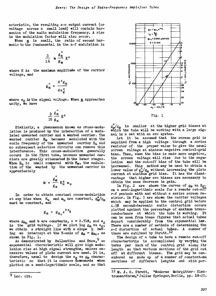
Henry: The Design of Radio -Frequency Amplifier Tubes
acteristic, the resulting a -c output current (orvoltage across a small load) will contain har-monics of the audio modulation frequency. A risein the modulation factor will also occur.
When m is small, the ratio of second har-monic to the fundamental in the a -f modulation is
3 gm E216 gm
where E is the maximum amplitude of the carriervoltage, and
11
gm
d 2gm
deg
where eg is the signal voltage. When m approachesunity, we have
3 gm E216 gm
Similarly, a phenomenon known as cross -modu-lation is produced by the interaction of a modu-lated unwanted carrier and a wanted carrier. Thewanted carrier Ew becomes modulated with theaudio frequency of the unwanted carrier Eu andno subsequent selective circuits can remove thisinterference. This cross -modulation generallyoccurs in the first tube, because unwanted car-riers are greatly attenuated tithe later stages.When Eu is small compared with Ew, the modula-tion of the wanted by the unwanted carrier isapproximately
$1
gmM = Eu mu
gm
In order to obtain constant cross -modulationat any bias when Eu and mu are constant, g:/gmmust be constant, and
beghoe g
wherewhere gmo and b are constants, E = 2.718, and egis the grid voltage. If we plot log gm vs eg,we obtain a straight line with a slope b hav-ing an intercept at the Y-axis of gm = gam, asshown in Fig. 1.
As demonstrated by Ballantine and Snow,9 anexponential characteristic will give high modu-lation rise at high signal strengths, unless ex-cessive values of plate current are used. It is,therefore, usual to design the ee vs gm charac-teristic so that it is concave downwards whenplotted on a semi -logarithmic scale, and so that
9 Loc. cit.
It
to
.eq - VOLTS
Fig. 1
-to
to
86
2
1.0.8
.e
.02
01
gm is smaller at the higher grid biases atwhich the tube will be working with a large sig-nal in a set with an ave system.
Let it be assumed that the screen grid issupplied from a high voltage through a series
resistor of the proper value to give the usualscreen voltage at minimum negative control -gridbias. Then, when the bias is made more negative,the screen voltage will rise due to the regu-
lation and the cut-off bias of the tube will beincreased. This method may be used to obtain alower value of 4/gm without increasing the platecurrent at minimum grid bias. It has the disad-
vantage that higher avc biases are necessary toobtain the same decrease in gain.
In Fig. 2 are shown the curves of gm vs Enon a semi -logarithmic scale for a remote cut-offr -f pentode with and without a series screen re-sistor. In Fig. 3 are shown the carrier voltageswhich may be applied to the control grid before
4.5% second -harmonic audio distortion occursplotted against the percentage of maximum trans -conductance at which the tube is working. It
can be seen from these figures that actual tubesdepart considerably from the exponential law.There are a number of methods of determining ther -f distortion of actual tubes. A number ofthese are outlined by Strutt.12
The design of a tube to have a remote cut-offcharacteristic is accomplished by varying the
turns per inch of the control grid along itslength so that various sections of the grid cutoff at different biases. The grid may be con-
sidered as made up of a number of constant -musections of different lengths and with per -
12 M. J. 0. Strutt, "Moderne Mehrgitter- Elek-tronenrohren"Julius Springer, Berlin, pp. 18-20.
207
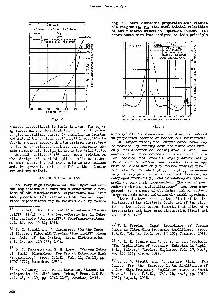
Vacuum Tube Design
1 1 I,--
TYPE 6K7_Er= 6.3V. Ec2r 0 V. Eb= 250V.-CURVE Ec2
100 V.- --- 250 V. THROUGH BY-PASSED90000 -OHM RESISTOR i
/I//
//////
....,/
/ ...////I
///
/I
-120 -100 -80 -60 -40 -20GRID NE VOLTS
Fig. 2
000
1000 tn800600
400 &'
2200
100 z80 <60
40 50
20 IA
10cct-
0
86
4
2
veances proportional to their lengths. The eg vsgm curves may then be calculated and added togetherto give a resultant curve. By changing the lengthsand mut s of the various sections, it is possible toobtain a curve approaching the desired character-istic. An experienced engineer can generally ob-tain a reasonable design in one or two trial tests.
Several articles13,14 have been written onthe design of variable -pitch grids by mathe-matical analysis, but these methods are tediousand, in general, not as useful as the simplercut -and -try method.
ULTRA -HIGH FREQUENCIES
At very high frequencies, the input and out-put capacitance of a tube are a considerable por-tion of the tuned -circuit capacitance and limitthe possible L/C ratios and the tuning range.These capacitances may be reduced15 ,16 by reduc-
13 G. Jobst, "On the Relation between ,Durch-griff, (1/4) and the Space -Charge Law in Tubeswith Variable IDurchgrifft," Telefunken-Zeitung,Vol. 12, pp. 29-44; 1931.
14 J. E. Schell. and F. Marguerre, "On the Theoryof Electron Tubes with Varying tDurchgrifft alongthe Axis of the System," Arch. Elektrotechn.,Vol. 28, pp. 210-233; 1934.
15 B. J. Thompson and G. M. Rose, "Vacuum Tubesof Small Dimensions for Use at Extremely HighFrequencies," Proc. I.R.E., Vol. 21, No.12, pp.1707-1722; December, 1933.
16 B. Salzberg and D. G. Burnside, "Recent De-velopments in Miniature Tubes," Proc. I.R.E.,Vol. 23, No.10, pp. 1142-1157; October, 1935.
ing all tube dimensions proportionately withoutaltering the Ib, gm, etc. until initial velocitiesof the electron become an important factor. Theacorn tubes have been designed on this principle
TYPE 6K7 CURVE EC2-1 - -- 100 V. FIXED
250 V. THROUGH _1
iJ
1
11 MODULATION
90000- OHMSERIES RESISTOR
=10010
I 11
I
II
II
1
1-I
I
1
1
I/ i
%
n1
,....__/
.06 .2 .4 .6 2 4
16
14 0
12
rl
10 at.
st
8 0
6 2cc
F40J
2 <
06 10 20 40 100
PERCENTAGE OF MAXIMUM TRANCONDUCTANCE
Fig. 3
although all the dimensions could not be reducedin proportion because of mechanical limitations.
In larger tubes, the output capacitance maybe reduced by cutting down the plate area untilonly the electron collecting area is left. Re-ductionofinput capacitance is a difficult prob-lem because the area is largely determined bythe size of the cathode, and because the spacingsmust be close not only to reduce transit timel7but also to provide high gm. High gm is neces-sary if any gain is to be realized, because, asmentioned previously, load impedances are usuallysmall at very high frequencies. The use of sec-
ondary -emission multiplication18 has been sug-gested as a means of obtaining high gm withoutlarge cathode areas and extremely small spacings.
Other factors such as the effect of the in-ductances of the electrode leads and of the elec-trodes themselves become important at ultra -highfrequencies akad have been discussed by Strutt andVan der Zie1.4
17 W. R. Ferris, "Input Resistance of VacuumTubes as Ultra -High -Frequency Amplifiers," Proc.I.R.E., Vol. 24, No.1, pp. 82-105; January, 1936.
18 J. L. H. Jonker and A. J. W. M. van Overbeek,"The Application of Secondary Emission in Ampli-fying Valves," Wireless Engineer, Vol. 15, No.3,pp. 150-156; March, 1938.
19 M. J. O. Strutt and A. Van der Ziel, "The
Causes for the Increase in the Admittances ofModern High -Frequency Amplifier Tubes on ShortWaves," Proc. I.R.E., Vol. 26, No.8, pp. 1011 -1031; August, 1938.
208
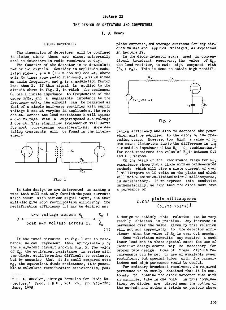
Lecture 22
THE DESIGN OF DETECTORS AND CONVERTERS
T. J. Henry
DIODE DETECTORS
The discussion of detectors will be confinedto diodes, since these are almost universallyused as detectors in radio receivers to -day.
The function of the detector is to demodulater -f or i-f signals. Consider an amplitude -modu-lated signal, e = E (1 + m cos at) cos wt, wherew is 2n times some radio frequency, a is 2n timesan audio frequency, and m is a modulation factorless than 1. If this signal is applied to thecircuit shown in Fig. 1, in which the condenser
C2 has a finite impedance to frequencies of theorder a/2n, and a negligible impedance to thefrequency w/2n, the circuit can be regarded asthat of a simple half -wave rectifier with supplyvoltage E cos wt varying in amplitude at the ratecos at. Across the load resistance R will appeara d -c voltage with a superimposed a -c voltage
A cos at. This simplified explanation will servefor most tube -design considerations. More de-tailed treatments will be found in the litera-ture.)
Fig. 1
In tube design we are interested in making atube that will not only furnish the peak currentswhich occur with maximum signal input, but thatwill also give good rectification efficiency. Therectification efficiency (D) may be defined as:
D =d -c voltage across RL
peak a -c voltage across Cl Es
Eo
(1)
If the tuned circuits in Fig. 1 are in reso-nance, we can represent them approximately bythe equivalent circuit shown in Fig. 2. The valueof Rs, the equivalent resistance in series withthe diode, would be rather difficult to evaluate,but by assuming that it is small compared withrd, the equivalent diode resistance, it is possi-ble to calculate rectification efficiencies, peak
1 H. A. Wheeler, "Design Formulas for Diode De-tectors," Proc. I.R.E., Vol. 26, pp. 745-780;June, 1938.
plate currents, and average currents for any cir-cuit values and applied voltages, as explainedin Lecture 19.
In the diode detector stage used in conven-tional broadcast receivers, the value of RL,the load resistor, is made high compared with(Rs + rd). This is done to obtain high rectifi-
Fig. 2
cation efficiency and also to decrease the powerwhich must be supplied to the diode by the pre-ceding stage. However, too high a value of RLcan cause distortion due to the difference in thea -c and d -c impedance of the RL - C2 combination.1For most receivers the value of RL is between 0.1and 0.5 megohm.
On the basis of the resistance range for RL,experience shows that a diode with an oxide -coated
cathode which will give a plate current of over1 milliampere at 10 volts on the plate and whichwill notteemission-limitedbelow 2 milliamperes,is satisfactory. If we express this conditionmathematically, we find that the diode must havea perveance of
0.032plate milliamperes
(plate volts)/
A design to satisfy this relation can be veryreadily obtained in practice. Any increase inperveance over the value given by this relationwill not add appreciably to the detector effi-ciency when the value of RL is over 0.1 megohm.
Some television circuits may require a muchlower load and in these special cases the use ofrectifier design charts may be necessary forproper tube design. Some of these circuit re-quirements can be met by use of available powerrectifiers, but special tubes with low capaci-tafices and high perveance would be useful.
For ordinary broadcast receivers, the requiredperveance is so easily obtained that it is cus-tomary to combine the diode detector tube withan amplifier tube in one bulb. In this combina-tion, two diodes are placed near the bottom ofthe cathode and either a triode or pentode above
209
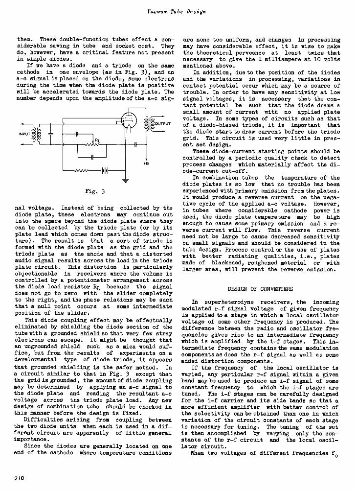
Vacuum Tube Design
them. These double -function tubes effect a con-siderable saving in tube and socket cost. Theydo, however, have a critical feature not presentin simple diodes.
If we have a diode and a triode on the samecathode in one envelope (as in Fig. 3), and ana -c signal is placed on the diode, some electronsduring the time when the diode plate is positivewill be accelerated towards the diode plate. Thenumber depends upon the amplitude of the a -c sig-
INPUT
Fig. 3
nal voltage. Instead of being collected by thediode plate, these electrons may continue outinto the space beyond the diode plate where theycan be collected by the triode plate (or by itsplate lead which comes down past the diode struc-ture). The result is that a sort of triode isformed with the diode plate as the grid and thetriode plate as the anode and that a distortedaudio signal results across the load in the triodeplate circuit. This distortion is particularlyobjectionable in receivers where the volume iscontrolled by a potentiometer arrangement acrossthe diode load resistor RL because the signaldoes not go to zero with the slider completelyto the right, and the phase relations may be suchthat a null point occurs at some intermediateposition of the slider.
This diode coupling effect may be effectuallyeliminated by shielding the diode section of thetube with a grounded shield so that very few strayelectrons can escape. It might be thought thatan ungrounded shield such as a mica would suf-fice, but from the results of experiments on adevelopmental type of diode -triode, it appears
that grounded shielding is the safer method. Ina circuit similar to that in Fig. 3 except thatthe grid is grounded, the amount of diode couplingmay be determined by applying an a -c signal tothe diode plate and reading the resultant a -cvoltage across the triode plate load. Any newdesign of combination tube should be checked inthis manner before the design is fixed.
Difficulties arising from coupling betweenthe two diode units when each is used in a dif-ferent circuit are apparently of little generalimportance.
Since the diodes are generally located on oneend of the cathode where temperature conditions
are none too uniform, and changes in processingmay have considerable effect, it is wise to makethe theoretical perveance at least twice thatnecessary to give the 1 milliampere at 10 voltsmentioned above.
In addition, due to the position of the diodesand the variations in processing, variations incontact potential occur which may be a source oftrouble. In order to have any sensitivity at lowsignal voltages, it is necessary that the con-tact potential be such that the diode draws asmall amount of current with no applied platevoltage. In some types of circuits such as thatof a diode -biased triode, it is important thatthe diode start to draw current before the triodegrid. This circuit is used very little in pres-ent set design.
These diode -current starting points should becontrolled by a periodic quality check to detectprocess changes which materially affect the di-ode -current cut-off.
In combination tubes the temperature of thediode plates is so low that no trouble has beenexperienced with primary emission from the plates.It would produce a reverse current on the nega-tive cycle of the applied a -c voltage. However,in tubes where considerable cathode power isused, the diode plate temperature may be highenough to cause some primary emission and a re-verse current will flow. This reverse currentneed not be large to cause decreased sensitivityon small signals and should be considered in thetube design. Process control or the use of plateswith better radiating qualities, i.e., platesmade of blackened, roughened material or withlarger area, will prevent the reverse emission.
DESIGN OF CONVERTERS
In superheterodyne receivers, the incomingmodulated r -f signal voltage of given frequencyis applied to a stage in which a local oscillatorvoltage of some other frequency is produced. Thedifference between the radio and oscillator fre-quencies gives rise to an intermediate frequencywhich is amplified by the i-f stages. This in-termediate frequency contains the same modulationcomponents as does the r -f signal as well as someadded distortion components.
If the frequency of the local oscillator isvaried, any particular r -f signal within a givenband maybe used to produce an i-f signal of someconstant frequency to which the i-f stages aretuned. The i-f stages can be carefully designedfor the i-f carrier and its side bands so that amore efficient amplifier with better control ofthe selectivity can be obtained than one in whichvariation of the circuit constants of each stageis necessary for tuning. The tuning of the setis then accomplished by varying only the con-stants of the r -f circuit and the local oscil-lator circuit.
When two voltages of different frequencies fo
210
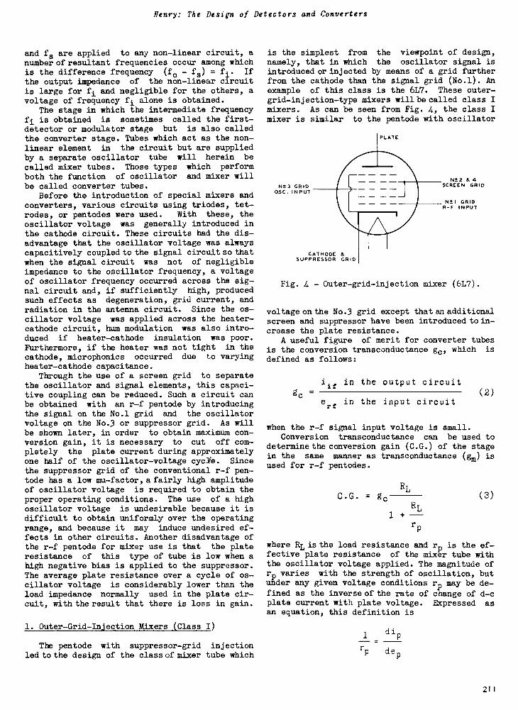
Henry: The Design of Detectors and Converters
and fs are applied to any non-linear circuit, anumber of resultant frequencies occur among whichis the difference frequency (fm - fs) = If
the output impedance of the non-linear circuitis large for fi and negligible for the others, avoltage of frequency fi alone is obtained.
The stage in which the intermediate frequencyfi is obtained is sometimes called the first -
detector or modulator stage but is also calledthe converter stage. Tubes which act as the non-linear element in the circuit but are suppliedby a separate oscillator tube will herein be
called mixer tubes. Those types which performboth the function of oscillator and mixer willbe called converter tubes.
Before the introduction of special mixers andconverters, various circuits using triodes, tet-rodes, or pentodes were used. With these, theoscillator voltage was generally introduced inthe cathode circuit. These circuits had the dis-advantage that the oscillator voltage was alwayscapacitively coupled to the signal circuit so thatwhen the signal circuit was not of negligibleimpedance to the oscillator frequency, a voltageof oscillator frequency occurred across the sig-nal circuit and, if sufficiently high, producedsuch effects as degeneration, grid current, andradiation in the antenna circuit. Since the os-cillator voltage was applied across the heater -cathode circuit, hum modulation was also intro-duced if heater -cathode insulation was poor.Furthermore, if the heater was not tight in the
cathode, microphonics occurred due to varyingheater -cathode capacitance.
Through the use of a screen grid to separatethe oscillator and signal elements, this capaci-tive coupling can be reduced. Such a circuit canbe obtained with an r -f pentode by introducingthe signal on the No.1 grid and the oscillatorvoltage on the No.3 or suppressor grid. As willbe shown later, in order to obtain maximum con-version gain, it is necessary to cut off com-pletely the plate current during approximatelyone half of the oscillator -voltage cycle. Sincethe suppressor grid of the conventional r -f pen-tode has a low mu -factor, a fairly high amplitudeof oscillator voltage is required to obtain theproper operating conditions. The use of a highoscillator voltage is undesirable because it isdifficult to obtain uniformly over the operatingrange, and because it may induce undesired ef-fects in other circuits. Another disadvantage ofthe r -f pentode for mixer use is that the plateresistance of this type of tube is low when ahigh negative bias is applied to the suppressor.The average plate resistance over a cycle of os-cillator voltage is considerably lower than theload impedance normally used in the plate cir-cuit, with the result that there is loss in gain.
1. Outer -Grid -Injection Mixers (Class I)
The pentode with suppressor -grid injectionled to the design of the class of mixer tube which
is the simplest from the viewpoint of design,namely, that in which the oscillator signal isintroduced or injected by means of a grid furtherfrom the cathode than the signal grid (No.1). Anexample of this class is the 6L7. These outer -
grid -injection -type mixers will be called class Imixers. As can be seen from Fig. 4, the class Imixer is similar to the pentode with oscillator
PLATE
N53 GRIDOSC. INPUT
CATHODESUPPRESSOR GRID
N22 & 4SCREEN GRID
NI! GRIDR -F INPUT
Fig. 4 - Outer -grid -injection mixer (6L7).
voltage on the No.3 grid except that an additionalscreen and suppressor have been introduced to in-crease the plate resistance.
A useful figure of merit for converter tubesis the conversion transconductance gm, which is
defined as follows:
ge -i
in the output circuit
err in the input circuit(2)
when the r -f signal input voltage is small.Conversion transconductance can be used to
determine the conversion gain (C.G.) of the stagein the same manner as transconductance (gm) isused for r -f pentodes.
C.G. = gcRL
1 + -r
RL( 3)
where RI, is the load resistance and r is the ef-fective plate resistance of the mixer tube withthe oscillator voltage applied. The magnitude ofrp varies with the strength of oscillation, butunder any given voltage conditions rp may be de-
fined as the inverse of the rate of change of d -cplate current with plate voltage. Expressed asan equation, this definition is
1dip
rp de
211
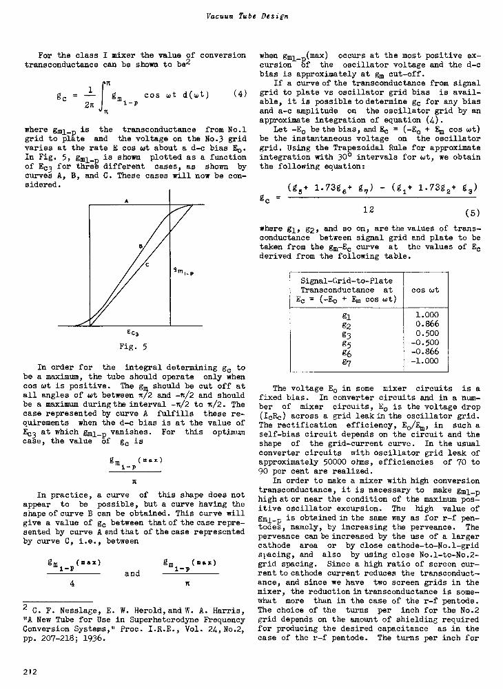
Vacuum Tube Design
For the class I mixer the value of conversiontransconductance can be shown to be2
gc1
2n "-1-P
cos wt d(wt) (4)
where gml_p is the transconductance from No.1grid to plate and the voltage on the No.3 gridvaries at the rate E cos wt about a d -c bias E0.In Fig. 5, gml_ is shown plotted as a functionof Ec3 for three different cases, as shown bycurves A, B, and C. These cases will now be con-sidered.
Ec3
Fig. 5
In order for the integral determining gc tobe a maximum, the tube should operate only whencos wt is positive. The g should be cut off atall angles of wt between n/2 and -n/2 and shouldbe a maximum during the interval -n/2 to n/2. Thecase represented by curve A fulfills these re-quirements when the d -c bias is at the value ofEc3 at which gml_p vanishes. For this optimumcase, the value of gc is
gm (max)1-p
In practice, a curve of this shape does notappear to be possible, but a curve having theshape of curve B can be obtained. This curve willgive a value of gc between that of the case repre-sented by curve A and that of the case representedby curve C, i.e., between
gmi-p(max) gmli-p(max)and4
2 C. F. Nesslage, E. W. Herold, and W. A. Harris,"A New Tube for Use in Superheterodyne FrequencyConversion Systems," Proc. I.R.E., Vol. 24,No.2,pp. 207-218; 1936.
when gml_p(max) occurs at the most positive ex-cursion of the oscillator voltage and the d -cbias is approximately at gm cut-off.
If a curve of the transconductance from signalgrid to plate vs oscillator grid bias is avail-able, it is possible to determine gc for any biasand a -c amplitude on the oscillator grid by anapproximate integration of equation (4).
Let -E0 be the bias, and Ec = (-E0 + Em cos wt)be the instantaneous voltage on the oscillatorgrid. Using the Trapezoidal Rule for approximateintegration with 30° intervals for wt, we obtainthe following equation:
g. =(g5+ 1'73ge g7) (g1+ l.73g2+ g3)
12(5)
where gl, g2, and so on, are the values of trans -
conductance between signal grid and plate to betaken from the gm-Ec curve at the values of Ecderived from the following table.
Signal -Grid -to -Plate
Transconductance atEc = (-E0 + Em cos wt)
cos wt
gl 1.000
g2 0.866
g3 0.500
g5-0.500
g6 -0.866
g7 -1.000
The voltage E0 in some mixer circuits is afixed bias. In converter circuits and in a num-ber of mixer circuits, E0 is the voltage drop(IcRc) across a grid leak in the oscillator grid.The rectification efficiency, Eo/Em, in such aself -bias circuit depends on the circuit and theshape of the grid -current curve. In the usualconverter circuits with oscillator grid leak ofapproximately 50000 ohms, efficiencies of 70 to90 per cent are realized.
In order to make a mixer with high conversiontransconductance, it is necessary to make gml_phigh at or near the condition of the maximum pos-itive oscillator excursion. The high value ofgml_p is obtained in the same way as for r -f pen-todes, namely, by increasing the perveance. Theperveance can be increased by the use of a largercathode area or by close cathode-to-No.1-gridspacing, and also by using close No.1-to-No.2-grid spacing. Since a high ratio of screen cur-rent to cathode current reduces the transconduct-ance, and since we have two screen grids in themixer, the reduction in transconductance is some-what more than in the case of the r -f pentode.The choice of the turns per inch for the No.2grid depends on the amount of shielding requiredfor producing the desired capacitance as in thecase of the r -f pentode. The turns per inch for
212
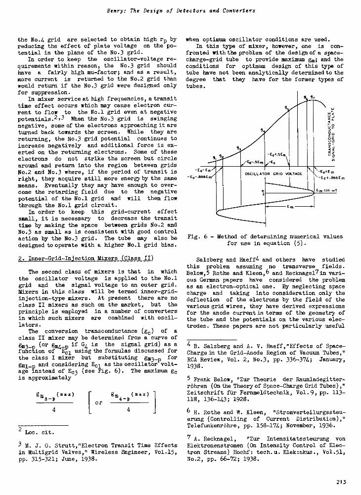
Henry: The Design of Detectors and Converters
the No.4 grid are selected to obtain high rp byreducing the effect of plate voltage on the po-tential in the plane of the No.3 grid.
In order to keep the oscillator -voltage re-
quirements within reason, the No.3 grid should
have a fairly high mu -factor; and as a result,
more current is returned to the No.2 grid thanwould return if the No.3 grid were designed onlyfor suppression.
In mixer service at high frequencies, a transittime effect occurs which may cause electron cur-rent to flow to the No.1 grid even at negativepotentials.2,3 When the No.3 grid is swingingnegative, some of the electrons approaching it areturned back towards the screen. While they are
returning, the No.3 grid potential continues to
increase negatively and additional force is ex-erted on the returning electrons. Some of theseelectrons do not strike the screen but circlearound and return into the region between gridsNo.2 and No.3 where, if the period of transit isright, they acquire still more energy by the samemeans. Eventually they may have enough to over-come the retarding field due to the negativepotential of the No.1 grid and will then flowthrough the No.1 grid circuit.
In order to keep this grid -current effect
small, it is necessary to decrease the transittime by making the space between grids No.2 andNo.3 as small as is consistent with good controlaction by the No.3 grid. The tube may also be
designed to operate with a higher No.1 grid bias.
2. Inner -Grid -Injection Mixers (Class II)
The second class of mixers is that in whichthe oscillator voltage is applied to the No.1grid and the signal voltage to an outer grid.Mixers in this class will be termed inner -grid -
injection -type mixers. At present there are noclass II mixers as such on the market, but the
principle is employed in a number of convertersin which such mixers are combined with oscil-lators.
The conversion transconductance (gc) of a
class II mixer may be determined from a curve ofgm3_n (or gm4_, if G4 is the signal grid) as afunction of E4 using the formulas discussed forthe class I mixer but substituting gm3_p forgml_p and considering Eci as the oscillator volt-age instead of Ec3 (see Fig. 6). The maximum gcis approximately
when optimum oscillator conditions are used.In this type of mixer, however, one is con-
fronted with the problem of the design of a space -charge -grid tube to provide maximum gm; and theconditions for optimum design of this type oftube have not been analytically determined to thedegree that they have for the former types oftubes.
- E0- Ern."'
- E0 -.866 E
-E.-F.5 Ern
0/-E0-.5Em
9 7
OSCILLATOR GRID VOLTAGE
3
-E0+.866Em
Em cos tut
Em
Fig. 6 - Method of determining numerical valuesfor use in equation (5).
Salzberg and Haeff4 and others have studiedthis problem assuming no transverse fields.Below,5 Rothe and Kleen,6 and Recknagel7in vari-ous German papers have considered the problemas an electron -optical one. By neglecting spacecharge and taking into consideration only thedeflection of the electrons by the field of thevarious grid wires, they have derived expressionsfor the anode current in terms of the geometry ofthe tube and the potentials on the various elec-trodes. These papers are not pArticularly useful
4 B. Salzberg and A. V. Haeff,"Effects of Space -
Charge in the Grid -Anode Region of Vacuum Tubes,"
RCA Review, Vol. 2, No.3, pp. 336-374;1938.
January,
5 Frank Below, "Zur Theorie der Raumladegitter-rohren (On the Theory of Space -Charge Grid Tubes),"
gms-p (max)[ or
gm (max)4-p
Zeitschrift fur Fernmeldtechnik, Vol.9,pp. 113-118, 136-143; 1928.
4 4 6 H. Rothe and W. Kleen,erung (Controlling of
"Stromverteilurgssteu-Current Distribution),"
2Loc. cit.
3 M. J. 0. Strutt,"Electron Transit Time Effectsin Multigrid Valves," Wireless Engineer, Vol.15,pp. 315-321; June, 1938.
Telefunkenrohre, pp. 158-174; November, 1936.
7 A. Recknagel, "Zur Intensitatssteurung vonElektronenstromen (On Intensity Control of Elec-tron Streams) Hochf: tech.u. Elek:akus., Vol.51,No.2, pp. 66-72; 1938.
213
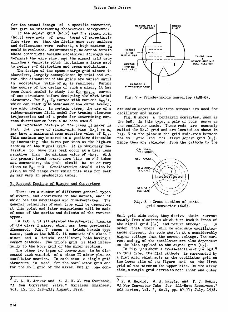
Vacuum Tube Design
for the actual design of a specific converter,but give an interesting theoretical background.
If the screen grid (No.2) and the signal grid(No.3) were made of many turns of exceedinglyfine wire so that the fields were very uniformand deflections were reduced, a high maximum gmwould be realized. Unfortunately, we cannot attainthese conditions because mechanical strength de-termines the wire size, and the signal grid usu-ally has a variable pitch (including a large gap)to reduce r -f distortion and cross -modulation.
The design of the space -charge -grid mixers istherefore, largely accomplished by trial and er-ror. The dimensions of the grids are varied untilan acceptable value of gc is realized. Duringthe course of the design of such a mixer, it hasbeen found useful to study the Ecl-gm3_p curvesof one structure before designing the next trialstructure. The Ec1-Ib curves with various Ec31s,which can readily be obtained on the curve tracer,are also useful. In certain cases, the use of arubber -membrane field model for tracing electrontrajectories and of a probe for determining cur-rent distribution have also been used.8
An important feature of the class II mixer isthat the curve of signal -grid bias (Ecs) vs gcmay have a maximum at some negative value of Ec3.This maximum may be moved in a positive directionby increasing the turns per inch on the high -musection of the signal grid. It is obviously de-sirable to have this peak occur at a bias lessnegative than the minimum value of -Ec3. Withthe present trend toward zero bias on r -f tubesand converters, the peak should be at or veryclose to Ec3 = 0. Consideration should also begiven to the range over which this bias for peakgc may vary in production tubes.
3. Present Designs of Mixers and Converters
There are a number of different general typesof mixers and converters on the market, each ofwhich has its advantages and disadvantages. Thegeneral principles of each type will be describedat this point and later comparisons will be madeof some of the merits and defects of the varioustypes.
In Fig. 4 is illustrated the schematic diagramof the class I mixer, which has been previouslydfscussed. Fig. 7 shows a triode-hexode-typemixer, such as the 6J8 -G. It consists of a class Imixer and a triode oscillator, both having acommon cathode. The triode grid is tied inter-nally to the No.3 grid of the mixer section.
The other two types of converters to be dis-cussed each consist of a class II mixer plus anoscillator section. In each case a single gridstructure is used for the oscillator grid andfor the No.1 grid of the mixer, but in one con -
8J. L. H. Jonker and A. J. W. M. van Overbeek,
"A New Converter Valve," Wireless Engineer,Vol. 15, pp. 423-431; August, 1938.
HEXODE PLATEI -F OUTPUT
HEXODEGRIDS
N22 a N24
HEXODEGRID N2i
R -F INPUT
CATHODESUPPRESSOR GRID
TRIODEPLATE
TRIODE GRID
HEXODE GRID N2.3OSC. INJECTION
Fig. 7 - Triode-hexode converter (6J8 -G).
struction separate electron streams are used foroscillator and mixer.
Fig. 8 shows a pentagrid converter, such asthe 6A8. In this type, a pair of rods serve asthe oscillator anode. These rods are commonlycalled the No.2 grid and are located as shown inFig. 8 in the plane of the grid side -rods betweenthe No.1 grid and the first screen grid (G3).Since they are shielded from the cathode by the
OSC. GRID(NT I GRID)
OSC. ANODE
NT 4 GRID(SIGNAL)
N23 GRID(SCREEN)
Fig. 8 - Cross-section of penta-grid converter (6A8).
No.1 grid side -rods, they derive their currentmainly from electrons which turn back in front ofthe signal grid (G4) and return through G3. Inorder that there will be adequate oscillator -anode current, the rods must be at a considerablyhigher voltage than the screen voltage. The cur-rent and gm of the oscillator are also dependenton the bias applied to the signal grid (G4).
In Fig. 9 is shown a cross-section of the 6K8.9In this type, the flat cathode is surrounded bya flat grid which acts as the oscillator grid onthe lower side of the figure and as the firstgrid of the mixer on the upper side. On the mixerside, a single grid serves as both inner and outer
9 E. W. Herold, W. A. Harris, and T. J. Henry,"A New Converter Tube for All -Wave Receivers,"RCA Review, Vol. 3, No.1, pp. 67-77; July, 1938.
214

Henry: The Design of Detectors and Converters
screen grid. The screen grid and signal grid aresurroundedbya shield which separates the oscil-lator and mixer sections and also functions as asuppressor grid between G4 and PH x.
A converter type EK3 has latelybeenannouncedby the N. V. Philips' Glowlampworks in Hollandwhich also makes use of separate electron streamsfor the oscillator and mixer.8 In addition, the
SIGNAL GRIDG3HX
ANODEPHX
CATHODE
SHIELD
SCREEN GRIDG2HX G4HX
Fig. 9 - Cross-section of triode-hexode convertertype 6K8.
construction is such that very few electrons canreturn from in front of the signal grid to theregion of the No.1 grid.
4. Important Features of Converters
Desirable features in mixers or convertersare:
1) High conversion transconductance (gc)2) High plate resistance of the mixer (rp)3) Low cost4) Low cathode current5) Low coupling effects between oscillator
and input circuit6) Low frequency drift
a. with automatic volume control (avc)b. with supply voltagec. due to oscillator interlocking
7) Low input conductance8) High oscillator transconductance.
The high gc and rp need no further comment.Cost is, of course, a factor in all tube designbut in the case of the converters, it has had agreat deal to do with the choice of design.
5. Coupling Effects
With an inner -grid injection type of mixer,the negative space charge in the vicinity of the
8 Loc. cit.
control (signal) grid increases10 /11 as the os-cillator grid becomes more positive. This in-crease in negative space charge tends to driveelectrons out through the control -grid circuit.The capacitance between oscillator grid and con-trol grid has the opposite effect, that is, apositive increment of voltage on the oscillatorgrid will tend to induce a negative charge on thecontrol grid and draw electrons in through thecontrol -grid circuit. If, as is customary, theoscillator frequency is higher than the signalfrequency, the input circuit offers capacitivereactance to the oscillator frequency and thevariation in space charge will produce a voltageout of phase with the oscillator voltage. Thiselectron coupling acts as a negative capacitancefrom oscillator grid to signal grid. The effectbecomes more important at high frequencies be-cause, if we keep the intermediate frequency con-stant, the signal and oscillator frequencies havea lower ratio and, therefore, the input -circuit
impedance will become appreciable at oscillatorfrequency so that higher voltages of oscillatorfrequency will be developed across the signalcircuit. With higher oscillator frequency thansignal frequency, this induced voltage of oscil-lator frequency on the signal grid tends to re-duce gc. With lower oscillator frequency thansignal frequency, it tends to increase gc.
The negative capacitance due to space -chargecoupling can generally be neutralized for any par-ticular frequency by connecting an external capac-itance from oscillator grid to signal grid,8,11but at very high frequencies where transit timebecomes a factor, the use of a resistance in se-ries with the capacitance3 may be required. Thismethod of neutralization is not entirely satisfac-tory. It has been observed that the use of a neu-tralizing capacitance increases frequency driftin the 6K8. The Philips' Glowlampworks use abuilt-in neutralizing capacitance and resistancein the type EK3. They state that frequency driftis increased by this neutralization but is stilllow enough to be satisfactory.
Outer -grid -injection tubes also show somespace -charge coupling due to electrons returningfrom the oscillator grid to the signal -grid re-gion but the effect is slight. In the inner -gridinjection type, space -charge coupling is inher-ently present because the space charge near thesignal grid must vary at oscillator frequency.
3 Loc. cit.
10 W. A. Harris, "The Application of Superheter-odyne Frequency Conversion Systems to MultirangeReceivers," Proc. I.R.E., Vol. 23, pp. 279-295;1933.
11 M. J. 0. Strutt, "Performance of Some Typesof Frequency Changers in All Wave Receivers,"Wireless Engineer, Vol. 14, pp. 184-192; 1937.
215
Vacuum Tube Design
6. Oscillator -Frequency Drift8,9 ,11
The oscillator frequency in most convertersvaries with the bias on the signal grid. Thisvariation is of sufficient magnitude in the 6A8and similar converters to cause considerable dif-ficulty in the high -frequency bands where a per-centage change in oscillator frequency will causea much larger percentage change in the beat fre-quency between a given r -f signal and the oscil-lator frequency.
If a fading r -f signal is tuned in, the vari-ation of the avc bias may be sufficient to causethe station to swing in and out of the band. Amore important effect is the difficulty encoun-tered in tuning.9 The magnitude of the outputwill differ when one tunes in from the higher- orthe lower -frequency end of the dial to a stationwith a large signal. Considerable readjustmentmay be necessary to obtain optimum tuning.
Change of frequency with change in signal -gridbias may be due to a change in the magnitude orthe phase angle of the oscillator gm, to a changein the internal capacitances of the tube, or toa combination of these effects. An out -of -phase
component in the transconductance will act asadditional capacitance or inductance in the os-cillator circuit, and a change in phase angle,or in magnitude of gm, will change the value ofthis effective capacitance or inductance.
In the pentagrid converter, the oscillatoranode derives most of its electron supply fromthe electrons returning through the screen fromthe G3 -G, region. Changes in signal -grid biasaffect both the number and the paths of the elec-trons returning to the oscillator anode and haveconsiderable effect on the magnitude of gm andalso on the phase angle of gm (due to transittime) at high frequencies.3,8
To reduce this oscillator drift with frequen-cy, a designer can put the oscillator section ona separate electron stream from that of the mixersection. This arrangement was employed in the6K8 with the result that the frequency drift wasvery much reduced.9 Other factors, such as thechange in input capacitance with variations ofsignal -grid bias, cause some residual frequencydrift with avc in both inner- and outer -grid in-jection types of converters, but with separateshielded electron streams the effect is small.
Frequency drift may also occur when the supplyvoltage to the converter elements is varied. Thismay happen when the line voltage fluctuates; or
in a set where the regulation of the rectifierfilter circuit is not perfect, fluctuation in the
3 Loc. cit
8 Loc. cit
9 Loc. cit.
11 Loc. cit.
voltages on the converter elements will occurwhen the average current drawn by the other tubesin the set changes due to signal. If the frequencydrift is large enough, the signal strength andavc bias on the other tubes in the set vary, anda type of audio -frequency motor -boating known as"flutter" may occur at high input signals if thetime constants of the circuits are favorable. Thiseffect can be reduced by adequate by-passing ofthe screen and oscillator -anode supplies, butsuch by-passing, of course, causes extra expense.Measurements usually show less fluttering on theouter -grid injection type of converter but thereason is not well understood. It may be due inparttofactors other than those discussed above.
7. Interlocking
At high signal inputs to the 6A8, an effectknown as "interlocking" occurs. Interlocking isdue to the signal -frequency pulses of electronsfrom in front of the signal grid which return tothe oscillator anode and tend to pull the oscil-lator frequency into step with the signal fre-quency.10 This effect is small in types wherethe oscillator is on a separate electron stream.
8. Input Conductance
High input conductance in a converter loadsthe tuned input circuit, broadens the tuning, anddecreases the gain. In the case of the outer -
grid -injection mixers, the input conductance in-creases with frequency in a manner similar to theincrease of conductance in the conventional triodeor r -f pentode. Moreover, it has been observedthat under the oscillating condition the conduct-ance is higher than might be expected from conven-tional tube considerations. Measurements of inputconductance under static conditions show that itincreases with increasingly negative oscillator -grid bias.
The increase in conductance is apparently dueto the electrons which return from the oscillator -grid region to the No.1 grid -cathode region. Whentheir return is prevented, this variation of inputconductance with oscillator -grid bias may begreatly reduced. One method of reducing the num-ber of returning electrons is by the use of beamprinciples similar to those used in the PhilipsEK3.8 Electron current to the No.1 grid willalso be reduced.
The input conductance of inner -grid -injectionconverters is generally low and may even be nega-tive.11
9. Signal -Grid Current
Signal -grid current in outer -grid -injection
mixers has been previously discussed. This phe-
10 Loc. cit.
216
Henry: The Design of Detectors and Converters
nomenon has also been observed in inner -grid -in-jection converters to a smaller degree, althoughthe reason for its occurrence is not clear.
10. Oscillator Transconductance
The magnitude of the gm of the oscillator isimportant because at high frequencies the circuitlosses become greater and a higher gm oscillatoris desirable in order to get adequate excitation.9
In the pentagrid converter, gm can be increasedby using a larger oscillator anode, but a lossof gc or a higher cathode current will result.
In the 6K8, the oscillator gm is quite highbecause of the large amount of cathode area de-voted to it. "Paths rectangular cathode, one halfof the cathode is used for the oscillator and withthe other half it is possible to get enough per-veance to operate the mixer section with a fairamount of gc.
In the outer -grid -injection converters, theoscillator and mixer sections in practice aremounted one above the other; and in order to getadequate perveance for the mixer section, theoscillator uses less than half of the cathodelength. Since it is convenient for stem connec-tions to mount the oscillator section at the bot-tom, the end -losses are high in this section andvariations in gm due to emission changes are tobe expected. It is possible to improve the gm bythe use of a rectangular cathode or by the use ofa larger cathode with more heater power. The rec-tangular cathode would increase the cost of analready expensive construction, and increasedheater power is not very acceptable in tubes foruse in both a -c and d -c sets.
11. Comparison of the Various Types of Converters
The pentagrid converter offers the advantagesof being relatively low in cost, but its large
9 Loc. cit.
frequency drift, lower oscillator gm, and elec-tron coupling are undesirable for high -frequencyuse. It can be used with an external oscillatortube to eliminate the first two objections butthis increases set cost.
The 6K8 is reasonably cheap, has low frequencydrift, and good oscillator gm, but still haselectron coupling. Because the 6K8 lacks sym-metry, distortion of its parts during manufactureproduces greater changes in characteristics thanoccur in types having symmetrical structures.The principle of separate electron streams foroscillator and mixer could be applied to sym-metrical structures (as in the Philips EK3) butthe cost would probably be high.
The outer -grid -injection mixer in which beamprinciples are used can be designed to have allthe desirable features listed above except theone of low cost for the converter stage. Low costis precluded since a separate oscillator tube isrequired. It does not appear practical to builda tube combining an outer -grid -injection mixerwith an oscillator having as high a gc and oscil-lator gm as are obtainable with the inner -grid -injection converter using the same heater power.
The choice of a converter or mixer design,therefore, depends largely on properly balancingeconomy and performance.
12. Application Tests
All new designs of tubes should have applica-tion tests when there is any doubt about theirperformance in actual circuits; but in convertersand mixers, so many factors are involved that athorough study of their performance under actualoperating conditions is extremely desirable, es-peciallyin the high -frequency bands. Other dif-ficulties which have not been discussed abovebut which should be investigated in applicationtests are hum, hiss, off -resonance microphonics,blocking, and variation in performance over theexpected range of oscillator excitation.
217
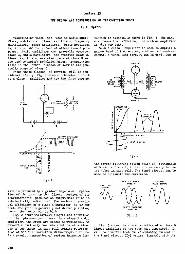
Lecture 23
THE DESIGN AND CONSTRUCTION OF TRANSMITTING TUBES
E. E. Spitzer
Transmitting tubes are used as audio ampli-fiers, modulators, linear amplifiers, frequencymultipliers, power amplifiers, plate -modulatedamplifiers, and for a host of miscellaneous pur-poses. Audio amplifiers are generally operatedclass A, while modulators are operated class B.Linear amplifiers are also operated class B andare used to amplify modulated waves. Transmittingtubes in the other classes of service are gen-erally operated class C.
These three classes of service will be con-sidered briefly. Fig. 1 shows a schematic circuitof a class A amplifier and how the plate -current
INPUTSIGNAL
-GRID VOLTS I
INPUT SIGNAL I(5)
LOAD OUTPUTRESISTANCE VOLTAGE
OUTPUT SIGNAL (0)- - - - - - - - --
Fig. 1
wave is produced by a grid -voltage wave. Opera-tion of the tube on the linear portion of itscharacteristic produces an output wave which issubstantially undistorted. The maximum theoreti-cal efficiency of a class A amplifier is 50 percent. The grid is generally not driven positive;hence, the power gain is high.
Fig. 2 shows the circuit diagram and formationof the plate -current wave in a class B audioamplifier. The grids are biased approximately tocut-off so that only one tube conducts at a time.Use of two tubes in push-pull permits reproduc-tion of the full wave -form in the output circuit.As a result, generation of serious harmonic dis-
tortion is avoided, as shown in Fig.mum theoretical efficiency of suchis 78.5 per cent.
When a class B amplifier is usednarrow band of frequencies, such assignal, a tuned load circuit can be
TODRIVERSTAGE
OPERATINGPOINT
TUBE A
TUBE B
3. The maxi -an amplifier
to amplify aa broadcastused. Due to
LOAD
PLATECURRENT
A0 + I
GRID VOLTAGE
INPUT SIGNAL
Fig. 2
the strong filtering action which is obtainablewith such a circuit, it is not necessary to usetwo tubes in push-pull. The tuned circuit can bemade to eliminate the harmonics.
EXCITINGSIGNAL
PLATE CURRENTTUBE A
PLATE CURRENTTUBE B
Fig. 3
OUTPUTWAVE SHAPE
Fig. 4 shows the characteristics of a class Blinear amplifier of the type just described. It
will be observed that the circulating current inthe tuned circuit (IT) varies linearly with the
218
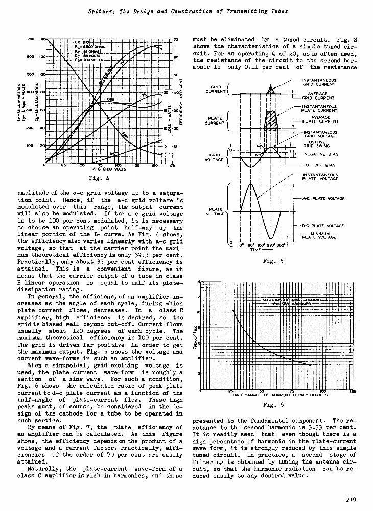
SPitzer: The Design and Construction of Transmitting Tubes
700 14
600 I
500
NO6.1
400a.g a2 1 4
,, 300iL
411.
200 40
100
i01111 =00..4 MIIl6SginiiiillAi
'P- EIN
m
=UM Aii-MomisVOLTS
MIL700 VOLTS
'%::: IPPOPIIIIIIIIIIII111111M01111
1A II
IIInommmmMwmam
milimimmmoieiImimn,
IIIIIAII..r..A.11.
n arn.m
mIIoimMIEMMmmilmolimaammummemommum,,AmmmummummAmmmoimmim
MEMO utrAi.L..PavoliiMMaw.A.
ip 0m.1114Ma .
111111112EMMI1111111111MMINIMMEKNAMMEMMOVAmMMEMMINIEWAMINIMMOMAMMMIIMMOMMAIMMMONSIMmommtmwhommommmummmommorworimmorsimmommmmem.mmmwmnummdmmmmmummomm.mmmmrammemmwimmommmummommmammMEWAI2MIMPIPIMPMMIMaViAMM7% mm
IMMOm mom!.mmpit-mmom
I
mm
mows
II
1
pia mon.=
5,E
JI
.g
-
..
A -C GRID VOLTS
Fig. 4
125 ISO
GO
50
40;
30 6
1.76
20
175
amplitude of the a -c grid voltage up to a satura-tion point. Hence, if the a -c grid voltage ismodulated over this range, the output currentwill also be modulated. If the a -c grid voltageis to be 100 per cent modulated, it is necessaryto choose an operating point half -way up thelinear portion of the IT curve. As Fig. 4 shows,the efficiency also varies linearly with a -c gridvoltage, so that at the carrier point the maxi-mum theoretical efficiency is only 39.3 per cent.Practically, only about 33 per cent efficiency isattained. This is a convenient figure, as itmeans that the carrier output of a tube in classB linear operation is equal to half its plate -dissipation rating.
In general, the efficiency of an amplifier in-creases as the angle of each cycle, during whichplate current flows, decreases. In a class Camplifier, high efficiency is desired, so thegrid is biased well beyond cut-off. Current flowsusually about 120 degrees of each cycle. Themaximum theoretical efficiency is 100 per cent.The grid is driven far positive in order to getthe maximum output. Fig. 5 shows the voltage andcurrent wave -forms in such an amplifier.
When a sinusoidal, grid -exciting voltage is
used, the plate -current wave -form is roughly asection of a sine wave. For such a condition,Fig. 6 shows the calculated ratio of peak platecurrent to d -c plate current as a function of thehalf -angle of plate -current flow. These highpeaks must, of course, be considered in the de-sign of the cathode for a tube to be operated insuch service.
By means of Fig. 7, the plate efficiency ofan amplifier can be calculated. As this figureshows, the efficiency depends on the product of avoltage and a current factor. Practically, effi-ciencies of the order of 70 per cent are easilyattained.
Naturally, the plate -current wave -form of aclass C amplifier is rich in harmonics, and these
To must be eliminated by a tuned circuit. Fig. 8shows the characteristics of a simple tuned cir-cuit. For an operating Q of 20, as is often used,the resistance of the circuit to the second har-monic is only 0.11 per cent of the resistance
14
4
GRIDCURRENT
{PLATECURRENT
GRIDVOLTAGE
PLATEVOLTAGE
INSTANTANEOUSGRID CURRENT
AVERAGEIII
I
GRID CURRENT
INSTANTANEOUSPLATE CURRENT
AVERAGEPLATE CURRENT
-I- INSTANTANEOUSGRID VOLTAGE
POSITIVEGRID SWING
NEGATIVE BIAS
9o* leo* 270 360*TIME -0 -
Fig. 5
CUT-OFF BIAS
INSTANTANEOUSPLATE VOLTAGE
DC PLATE VOLTAGE
MINIMUMPLATE VOLTAGE
12-
a
ECTPut4IONS
E3OF s
AiwSSUMEDtulaR40-
30 73 10CHALF -ANGLE OF CURRENT FLOW - DEGREES
Fig. 6
presented to the fundamental component. The re-actance to the second harmonic is 3.33 per cent.It is readily seen that even though there is ahigh percentage of harmonic in the plate -currentwave -form, it is strongly reduced by this simpletuned circuit. In practice, a second stage offiltering is obtained by tuning the antenna cir-cuit, so that the harmonic radiation can be re-duced easily to any desired value.
2t9

Vacuum Tube Design
r102UUU9U5.
K0
7U
U 61
.. -Arge.137101: f7IFRIT71713MINN
IIMMMMMr.417tIalliThEWilleMEMEN
111M
ME111111111MCM6Jitionc11102E2WitElf
1 v..' 4IIINiMildith
OICIEt 2'mom1:MOMMMOMM
E MMM MMT1EM
1:::1IIIIIIMIIIIIIIII111111111111II1 116111111111111111MNOMMEMMOMMOMEM9IIIOOMMEMMEMEMMUMMMIII
"11111
1111111161
111
IMOMIGUMMEMIIIIMEMb441=1ME
V1111111 111ii...
..i11111111111
........ IuI 1m .... .I i.i.......
UMa1.IIIII1__i_i_ KmI m1M
N..M:vE
iM
E
tIM= ME E M
1
I a0 10 20 30 40 50 60 70 60
HALF -ANGLE OF CURRENT FLOW -DEGREES90
Fig. 7 - Class B and C amplifier efficiency.
100
The maximum ratings of transmitting tubes forclass C telegraph service are considered thebasic ratings, as the ratings for other classesof service can be derived from them. The maximumratings are given for d -c plate voltage, d -c platecurrent, plate input, plate dissipation, screenvoltage and input, suppressor voltage and input,grid bias and grid current. The maximum plateratings are determined by the original require-ments and design. In any case, the plate inputis not allowed to exceed four times the platedissipation, as higher values would require morethan 75 per cent efficiency, which would be very
difficult for all users to obtain.
1
LET wo =LC
(a) (b)
Zy
Zx
(b)
woL
cl
FUNDAMENTAL 2nd HARMONIC 3rd HARMONIC
zx/R zy/R zx/R zy/R zx/R zy/R
10 1 0 .0044 .0554 .0014 .0374
20 1 0 .0011 .0333 .00035 .0187
30 1 0 .00050 .0221 .00016 .0125
Fig. 8 - Characteristics of a simpletuned circuit.
Fig. 9 shows the maximum ratings807 for several classes of service.mental class C telegraph ratings wereby means of life tests. In the case
of the RCA -
The funds -
establishedof class C
RCA -807
Transmiiiing Beam Power Amplifier
As R -F Power Amplifier and Oscillator-Class C Telegraphy
Key -down conditions per tube without modulation
DC PLATE VOLTAGE 600 max. VoltsDC SCREEN VOLTAGE (Grid No. 2) 300 max. VoltsDC GRID VOLTAGE (Grid No. 1) -200 max. VoltsDC PLATE CURRENT 100 max. MilliamperesDC GRID CURRENT 5 max. MilliamperesPLATE INPUT 60 max. WattsSCREEN INPUT 3.5 max. WattsPLATE DISSIPATION 25 max. Watts
As Plate -Modulated R -F Power Amplifier-Class C Telephony
Carrier conditions per tube for use with a max. modulation factor of 1.0
DC PLATE VOLTAGE 475 max. VoltsDC SCREEN VOLTAGE (Grid No. MMMMMM 300 max. VoltsDC GRID VOLTAGE (Grid No. 1) -200 max. VoltsDC PLATE CURRENT 83 max. Milliamperes
5 max. MilliamperesPLATE INPUT 40 max. WattsSCREEN INPUT 2.5 max. WattsPLATE DISSIPATION 16.5 max. Watts
As R -F Power
Carrier conditions per tube
13,C PLATE VOLTAGE
Amplifier-Class B Telephonyfor use with a max. modulation factor of 1.0
DC SCREEN VOLTAGE (Grid No. 2)DC PLATE CURRENTPLATE INPUT ........ ..............
SCREEN INPUTPLATE DISSIPATION
Fig. 9
600 max. Volts300 max. Volts
80 max. Milliamperes37.5 max. Watts2.5 max. Watts25 max. Watts
telephone service, the ratings are given for car-rier conditions, that is, with no plate modula-
220

Spitzer: The Design and Construction of Transmitting Tubes
tion applied. It is well known that the power ina 100 per cent modulated wave (single frequencymodulation) is 50 per cent greater than in thecarrier wave alone. The rms voltage is greaterby a factor of 1, or roughly 1.25. These fac-tors are used in reducing the plate ratings forclass C telephone service. The plate -input and
dissipation ratings are reduced by the factor1/1.5 (= 66.7%) from the class C telegraph rat-ings. The plate voltage is reduced by the fac-tor 1/1.25 (= 80%).
For class B telephone service it is neces-sary to reduce the plate -input and plate -currentratings because of the low efficiency under car-rier conditions. An efficiency of 33 per centis assumed for rating purposes, and this fixesthe plate input at 150 per cent of the plate -dissipation rating. The plate -and screen -voltageratings are not reduced, since the r -f and d -c
voltage stresses on the tube are no more severethan in class C telegraph service. The plate -
current rating is reduced because of the reductionof input. It should be noted at this point thatthe product of plate current and voltage is higherthan the maximum plate input in some cases. The
product is purposely higher to allow the use offull input at reduced plate voltage, if desired.Such operation is possible with tubes of highperveance. However, all ratings are independent,that is, none of them may be exceeded.
Where tubes are designed primarily for the
amateur market, the plate -input watts per dollarof list price is made as high as possible forcompetitive reasons. Tubes designed for the laststage of broadcast transmitters must have a rat-ing approved by the Federal Communications Com-mission. For the purpose of readily limiting theradiated carrier power of such transmitters, theFCC limits the input power to the last stage byassuming certain efficiencies. For high-levelmodulated stages, the efficiencies are shown inTable I.
Table I
Rated Carrier PowerWatts
Plate EfficiencyPer cent
100 50
250 - 1000 60
2500 - 50000 65
For example, the RCA -833, which was designed fora 500 -watt, high-level, modulated carrier, has acarrier input of 500/0.6 = 835 watts.
Given the essential input ratings, the nextdecision is a choice of triode, tetrode, beamtetrode, or pentode construction. Triodes permitthe highest watts per dollar but require neutrali-zation. Table II gives some illustrative fig-ures on comparative triodes and multigrid tubes.
Table II
WATTS PER DOLLAR
(Max.Class C Telegraph InputWatts/$ of List Price)
Type Watts Price IN/$
809 75 $ 2.50 30.0
Triodes808805
200315
7.7513.50
25.823.3
833 1250 85.00 14.7898 200000 1650.00 121.0
807 60 3.50 17.1Tetrodes 814 180 17.50 10.3
& Pentodes 803
{350 34.50 10.1
861 1200 295.00 4.0
Tetrodes avoid neutralization within limits.
Above 45 megacycles very expensive constructionis required to avoid feedback due to the induct-ance of the screen lead. Beam tetrodes and pen-todes have the advantage of very low drivingpower. Whereas in triodes the grid must be drivenhighly positive to obtain the peak current pulses,in beam tetrodes and pentodes the necessary ac-celeration to the electrons is supplied by thescreen, so that the grid need not be driven farpositive and thus does not draw heavy grid cur-rent. Fig. 10 illustrates these statements veryclearly.
Pentodes have the additional advantage thatthey can be suppressor modulated. While sup-pressor modulation results in a big reduction ofcarrier output, the absence of heavy modulationtransformers often offsets this loss in mobileinstallations. Fig. 11 shows a typical suppres-sor -modulation characteristic. It will be notedthat the suppressor current is very low; hence,the modulation power required is very low. Itis difficult to obtain more than about 80 percent modulation due to the curvature of the char-acteristic.
The next step in design is to determine theperveance needed. It is calculated from the de-sired plate current and plate efficiency. FromFig. 12 it can be seen that practically it is un-desirable to swing the grid more positive than
the plate because the ratio of plate to grid cur-rent drops rapidly beyond this point, and as aresult high driving power is required. If the
plate and grid voltage are made equal in the sim-plified expression for the characteristic of atriode, the mu -factor drops out. It will be notedthat if plate current in milliamperes is read atEb = Ec = 100 volts, the value obtained is the
plate perveance of the tube in microam-
peres/volt3/2.
Details for calculating the perveance of any
structure will not be given here as they have
221
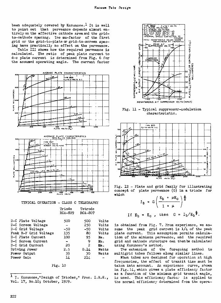
Vacuum Tube Design
been adequately covered by Kusunose.1 It is wellto point out that perveance depends almost en-tirelyon the effective cathode area and the grid -to -cathode spacing. The mu -factor of the firstgrid or the grid -to -plate or grid -to -screen spac-
ing have practically no effect on the perveance.Table III shows how the required perveance is
calculated. The ratio of peak plate current tod -c plate current is determined from Fig. 6 forthe assumed operating angle. The current factor
2
AVERAGE PLATE CHARACTERISTICS!WU
I 'NIP
j....S.1...........e
I
r7.11.2 VOLTS D.C.
P60044,
fee
60
WO
+40
+20200
+M
0 200 WO 600 800
Ec
MM
0
MWPLATE VOLTS (E6)
AVERAGE PLATE CHARACTERISTICSAS VARIABLE4.50I
E tT*2'TYPE
'SCfRE.E.:1
I
807VOLTS
I
= 2
400
50
0
+15
/111300 "III+10
5
200 40c-RMG
11111111-5VOLTS
+
EC
=0
100-1000/AVIIIIII -15
25Ec,=-20
/-- -40 100 200 3 400 500 646- ion
TYPICAL OPERATION
PLATE VOLTS
- CLASS C TELEGRAPHY
TriodeRCA -809
TetrodeRCA -807
D -C Plate Voltage 500 500 VoltsD -C Screen Voltage 250 VoltsD -C Grid Voltage -50 -50 VoltsPeak R -F Grid Voltage 135 80 VoltsD -C Plate Current 100 95 Ma.D -C Screen Current 9 Ma.D -C Grid Current 20 2 Ma.Driving Power 2.5 0.14 WattsPower Output 35 30 WattsPower Gain 14 214
Fig. 10
1 Y. Kusunose,"Design of Triodes," Proc. I.R.E.,Vol. 17, No.10; October, 1929.
,
2
210
2
<8
16
1.1 m
314
g4 02an aa.
TYPE 802 E1=6.3 VOLTSD -C PLATE VOLTS=500
-D-C SCREEN VOLTS=200D -C SUPPRESSOR VOLTS =-450-C GRID BIAS VOLTS= -90
-PEAK R -F GRID VOLTS =125INTERNAL SHIELD CONNECTED TO
CATHODE-NOTE : INSTANTANEOUS VALUES IGNORE
INSTANTANEOUS R -F COMPONENTS
"" 1..JPPPFFEASKSORFVOLT?--1
-
-
-
-65 0I
+65
2CARR
CONDITIER
S
k
%.,,,
I
i
'ICI,G"'
./- I-100 -50 +50
Ue.,
IS
a
O ,
cdi
40 13
30cn
201
10
0.
INSTANTANEOUS A-F SUPPRESSOR VOLTS ( NPUT)
Fig. 11 - Typical suppressor -modulationcharacteristic.
"T yPE 805
cr,o v0LT3 A.C.
500aAlFirp,005.rlinal..0300
_.......mi...5.-:-oo...,........
---'""°-.-.rrerilM,,,e
200,o
SO*
---
(3 111
10116111111 ..iii20
00
f ,111111,MN,,,,,i1IPreigubm.
100 i
0
,,T.
0 -17/4100;pliweirseglom1...'"1".."-
so
PLATE VOLTS (Es)
Fig. 12 - Plate and grid family for illustratingconcept of plate perveance (G) in a triode forwhich
Ib = G1 + µ
If Eb = Ec , then G = Ib/Ebt.
is obtained from Fig. 7. From experience, we as-sume the peak grid current is 1/4 of the peakplate current. This assumption permits calcula-tion of the minimum perveance, and the requiredgrid and cathode structure can then be calculatedusing Kusunosels method.
The extension of the foregoing method to
multigrid tubes follows along similar lines.When tubes are designed for operation at high
frequencies, the effect of transit time must betaken into account. An experience curve, shownin Fig.14,which gives a plate efficiency factoras a function of the minimum grid transit angle,is used. This efficiency factor is applied tothe normal efficiency determined from the opera -
222
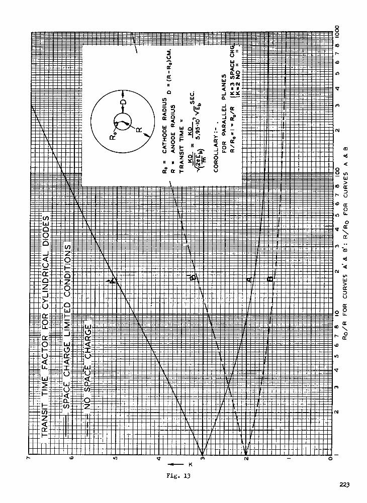
(I)
00_J
0C-E
CC
0cr.0
2
ton
a
,
Mmmui==========
aMimmmmimMIMSIMMOIILTEMEnn..MMMMO
mmMM=MMmaiMMMM26EMESE ==:-- ====MMMMMEIMMMIMMMMIMMrearallAMIMMEMEMalaMcommaiEschwanMEZZEIVILTM ===== =EMUWIIMMEMMOMMINIMBE EMOMIMMOMM
a MOMMIUMMWOMmMIWOMMOMMMO ===== MUM=========MMEM=======mEEEMMHOUNMEMEEMMEEMMM. EEEMEHEEEMEEEEEEEEEEN
MMEEEHEEEMEENEENEEEENEEMMENEEEMENEEMEEMEM
., EEMEENEEEMEEEEEMMEMEMOMEEMEEEIMEMMEMEEEEEEMEEMEEMEEMEMEEMEEMEE
a I SIMMIIIMININIMMINIMEN
EE
MMMMMWIMMMMMAIIMMOM
MMMMMMMMMM
IN
MMMMMMMM Mania
EMMMM MMMM WENN al.miin F.1..2.
-----------m
G . 1Z
i.
ANSOMEMOa
M.
CC S_om E===3
LI
=================================munummm MMMMMMM nmommommmoomummomm=mm======wrew=mmmommummwmumemnommammmmumumEEEMMEIEPTNEEEEEEEMEEEEMMINMIWIMMEEMMEEEE:qMEEKINNIMMEEEEEEEEEEEMEEEREEWgMEEEEEMENINEEEMEEMEREEEEEEEEEMEEUEEEEMEMEMEENEEENEEEMENEEMEEEEMEEEEMEMEEMEEMEENEMEEMEEMEENEEMEEMEMENEEMEMEMEEEEMEEMEEMEMEMEEMEEMEEMEMEEMEEMEEMEEMEMEEMEMEEMEMEMENEEMEEMEEMEEMEEEMEEEEENEMEEEEEMEMEEMEEMEKEEEEEEMEEMEMEEMEMEEEEEEMEEEMEEENEEEMENEEMEREENEEEREEMEEMEEEMEEMEEEEEEMWEEEENEENEEEMEEMEMMEIMMEMMINEMENVEMEMMIMMEMEMMINUMMINEMOMMIMMEMPIMEMEMMINIMENMINEMEMINIMISMIMMINSIMMINSIMMIKUNIMMENINIMMILMINNIMMUMMINSEEEE-E-= =-m: sias......-
.7:- m= ==.. = -1.:=
V1====EZ==.mmMM----MMMMM
E=
==,LJ--1<0 ..2
-- CLAN E EEm '''a.2 W MMMOMMMOIRMMMOOMMMIUMO
.1. . OMt == mommomm======mmommommwmommimmwm==mommmaimmmumm MMMMMMMMMMME11111.11E111.11111.=====.11==================111MMENIIIIIIIIMMINIINIMINM===MOWS EM=EUmEEEEMNEEEEEEEEEMMMONOMMEEMEMEMMEMEEEMEEEEMEEEEMEEEMEEMMEM REIMEEEEEEEMEEEEEEEEEEINEENEVIIIENIMEREEEEILIENEEEENIEIMENEENEEEEEMEEENEHEEMEMEMEEEMEEEEEEEENENNEEEMMEMMEENEEMEEHREMEEMEEEEMEEEEEEEEEE
H hEMEME1MEMUEMEENEMEMIEEME1NMEEEEUMIIIEINIMEEMEIEEIWEMEMMMMEMEKMMMUEEMMEEIMEMMEEMME
MINMIMMESMMMMIMMMENMMMSOMNMMMENMOMMINEENHDMMNOMMEMMMEMMNENI
====EE=6'22 '2
=MMMMIWAa====m
ME oMM=MOM= MMMMMMMUMMMMMIMM
MOW
1"= 6== =====--- --mw- ----v-----=-..-=--__=1 ---------__ - -"E. ----=====5===a1======WA=
0 0 0K
CO
00 0
CO cc
DIs u
O4:1
LO
cc
2 L9
In
Fig. 13
223
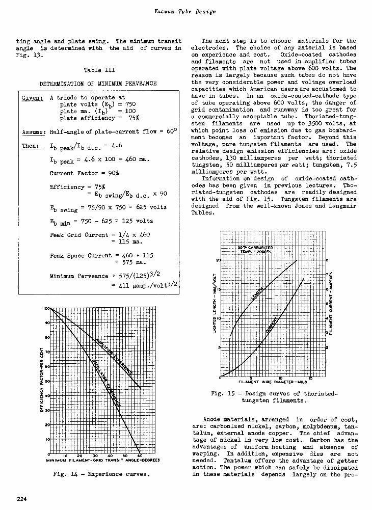
Vacuum Tube Design
ting angle and plate swing. The minimum transitangle is determined with the aid of curves inFig. 13.
Table III
DETERMINATION OF MINIMUM PERVEANCE
Given: A triode to operate atplate volts (Eb) = 750plate ma. (Ib) = 100plate efficiency = 75%
Assume: Half -angle of plate -current flow =
Then: Ib peak/Ib d.c. = 4.6
Ib peak = 4.6 x 100 = 460 ma.
Current Factor = 90%
Efficiency = 75%
= Eb swing/Eb d.c. x90
Eb swing = 75/90 x 750 = 625 volts
Eb min = 750 - 625 = 125 volts
Peak Grid Current = 1/4 x 460= 115 ma.
Peak Space Current
Minimum Perveance =
= 460 + 115= 575 ma.
575/(125)3/2
= 411 gamp./volt3/2
60°
90
80
o-70
aa
cc
8. 60
0o-
itC
)-
6 40
50
4
30
0
+.4
-1+0 10 20 30 40 50 60MINIMUM FILAMENT-GRID TRANSIT ANGLE-DEGREES
Fig. 14 - Experience curves.
The next step is to choose materials for theelectrodes. The choice of any material is basedon experience and cost. Oxide -coated cathodesand filaments are not used in amplifier tubesoperated with plate voltage above 600 volts. Thereason is largely because such tubes do not havethe very considerable power and voltage overloadcapacities which American users are accustomed tohave in tubes. In an oxide -coated -cathode typeof tube operating above 600 volts, the danger ofgrid contamination and runaway is too great fora commercially acceptable tube. Thoriated-tung-sten filaments are used up to 3500 volts, atwhich point loss of emission due to gas bombard-ment becomes an important factor. Beyond thisvoltage, pure tungsten filaments are used. The
relative design emission efficiencies are: oxidecathodes, 130 milliamperes per watt; thoriatedtungsten, 50 milliamperes per watt; tungsten, 7.5milliamperes per watt.
Information on design of oxide -coated cath-odes has been given in previous lectures. Tho-riated-tungsten cathodes are readily designedwith the aid of Fig. 15. Tungsten filaments aredesigned from the well-known Jones and LangmuirTables.
2 IS
W 10
S
_ -
r1 -I
r
304. cAaavai--Tcmp, *
SFILAMENT WIRE DIAMETER -MILS
7
6
5
4
2
2JI.
Fig. 15 - Design curves of thoriated-tungsten filaments.
Anode materials, arranged in order of cost,are: carbonized nickel, carbon, molybdenum, tan-talum, external anode copper. The chief advan-tage of nickel is very low cost. Carbon has theadvantages of uniform heating and absence ofwarping. In addition, expensive dies are notneeded. Tantalum offers the advantage of getteraction. The power which can safely be dissipatedin these materials depends largely on the pro-
224
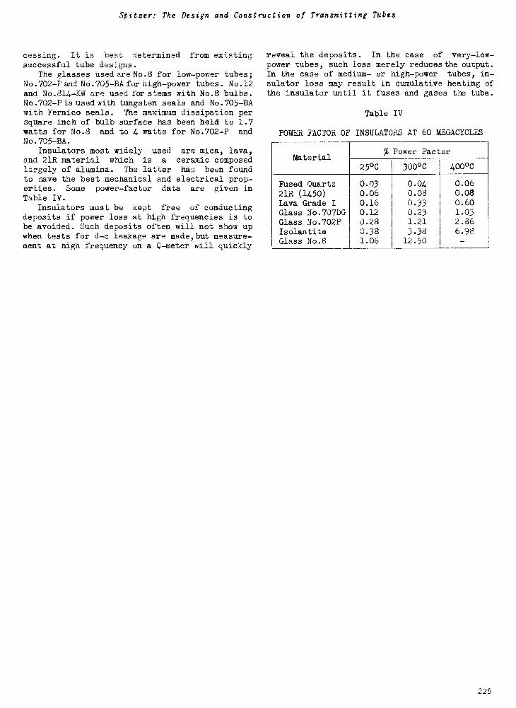
Spitzer: The Design and Construction of Transmitting Tubes
cessing. It is best determined from existingsuccessful tube designs.
The glasses used are No.8 for low -power tubes;No.702-P and No.705-BA for high -power tubes. No.12and No.814-KW are used for stems with No.8 bulbs.No.702-Pisusedwith tungsten seals and No.705-BAwith Fernico seals. The maximum dissipation persquare inch of bulb surface has been held to 1.7watts for No.8 and to 4 watts for No.702-P andNo.705-BA.
Insulators most widely used are mica, lava,and 21R material which is a ceramic composedlargely of alumina. The latter has been foundto have the best mechanical and electrical prop-erties. Some power -factor data are given inTable IV.
Insulators must be kept free of conductingdeposits if power loss at high frequencies is tobe avoided. Such deposits often will not show upwhen tests for d -c leakage are made,but measure-ment at high frequency on a Q -meter will quickly
reveal the deposits. In the case of very -low -
power tubes, such loss merely reduces the output.In the case of medium- or high -power tubes, in-sulator loss may result in cumulative heating ofthe insulator until it fuses and gases the tube.
Table IV
POWER FACTOR OF INSULATORS AT 60 MEGACYCLES
Material% Power Factor
25°C 300°C 400°C
Fused Quartz 0.03 0.04 0.06
21R (1450) 0.06 0.08 0.08Lava Grade I 0.16 0.33 0.60Glass No.707DG 0.12 0.23 1.03
Glass No.702P 0.28 1.21 2.86Isolantite 0.38 3.38 6.98
Glass No.8 1.06 12.50 -
225
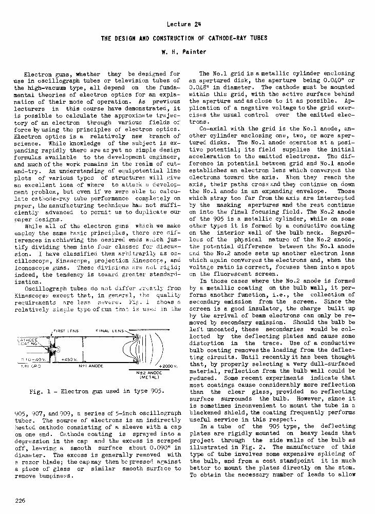
Lecture 24
THE DESIGN AND CONSTRUCTION OF CATHODE-RAY TUBES
W. H. Painter
Electron guns, whether they be designed foruse in oscillograph tubes or television tubes ofthe high -vacuum type, all depend on the funda-mental theories of electron optics for an expla-nation of their mode of operation. As previous
lecturers in this course have demonstrated, itis possible to calculate the approximate trajec-tory of an electron through various fields offorce by using the principles of electron optics.Electron optics is a relatively new branch of
science. While knowledge of the subject is ex-panding rapidly there are as yet no simple designformulas available to the development engineer,and much of the work remains in the realm of cut -and -try. An understanding of equipotential lineplots of various types of structures will givean excellent idea of where to attack 9 develop-ment problem, but even if we were able to calcu-late cathode-ray tube performance completely onpaper, the manufacturing technique has not suffi-ciently advanced to permit us to duplicate ourpaper designs.
While all of the electron guns which we makeemploy the same basic principles, there are dif-ferences in achieving the desired ends which jus-tify dividing them into four classes for discus-sion. I have classified them arbitrarily as os-cilloscope, Kinescope, projection Kinescope, andIconoscope guns. These divisions ere not rigid;indeed, the tendency is toward greeter standard-ization.
Oscillograph tubes do not differ ,:reatly fromKinescopes except that, in general, the quality
requirements are less severe. Fig. i shows a
relatively simple type of gun that is used in the
CATHODECOATING
n TO -40 V.NSI GRID
FINAL LENS
NSt ANODE +2000 V.
N!2 ANODE(METAL)
Fig. 1 - Electron gun used in type 905.
905, 907, and 909, a series of 5 -inch oscillograph
tubes. The source of electrons is an indirectlyheated cathode consisting of a sleeve with a capon one end. Cathode coating is sprayed into adepression in the cap and the excess is scrapedoff, leaving a smooth surface about 0.090" in
diameter. The excess is generally removed with
a razor blade; the cap may then be pressed againsta piece of glass or similar smooth surface to
remove bumpiness.
The No.1 grid is a metallic cylinder enclosingan apertured disk, the aperture being 0.040" or0.048" in diameter. The cathode must be mountedwithin this grid, with the active surface behindthe aperture and as close to it as possible. Ap-plication of a negative voltage to the grid exer-cises the usual control over the emitted elec-trons.
Co -axial with the grid is the No.1 anode, an-other cylinder enclosing one, two, or more aper-tured disks. The No.1 anode operates at a posi-tive potential; its field supplies the initialacceleration to the emitted electrons. The dif-ference in potential between grid and No.1 anodeestablishes an electron lens which converges theelectrons toward the axis. When they reach theaxis, their paths cross and they continue on downthe No.1 anode in an expanding envelope. Thosewhich stray too far from the axis are interceptedby the masking apertures and the rest continueon into the final focusing field. The No.2 anodeof the 905 is a metallic cylinder, while on someother types it is formed by a conductive coatingon the interior wall of the bulb neck. Regard-less of the physical nature of the No.2 anode,the potential difference between the No.1 anodeand the No.2 anode sets up another electron lenswhich again converges the electrons and, when thevoltage ratio is correct, focuses them into a spoton the fluorescent screen.
In those cases where the No.2 anode is formedby a metallic coating on the bulb wall, it per-forms another function, i.e., the collection ofsecondary emission from the screen. Since thescreen is a good insulator, the charge built upby the arrival of beam electrons can only be re-moved by secondary emission. Should the bulb beleft uncoated, these secondaries would be col-lected by the deflecting plates and cause somedistortion in the trace. Use of a conductivebulb coating removes the loading from the deflec-ting circuits. Until recently it has been thoughtthat, by properly selecting a very dull -surfacedmaterial, reflection from the bulb wall could bereduced. Some recent experiments indicate thatmost coatings cause considerably more reflectionthan the clear glass, provided no reflectingsurface surrounds the bulb. However, since itis sometimes inconvenient to mount the tube in ablackened shield, the coating frequently performsuseful service in this respect.
In a tube of the 905 type, the deflectingplates are rigidly mounted on heavy leads thatproject through the side walls of the bulb asillustrated in Fig. 2. The manufacture of thistype of tube involves some expensive splicing ofthe bulb, and from a cost standpoint it is muchbetter to mount the plates directly on the stem.To obtain the necessary number of leads to allow
226
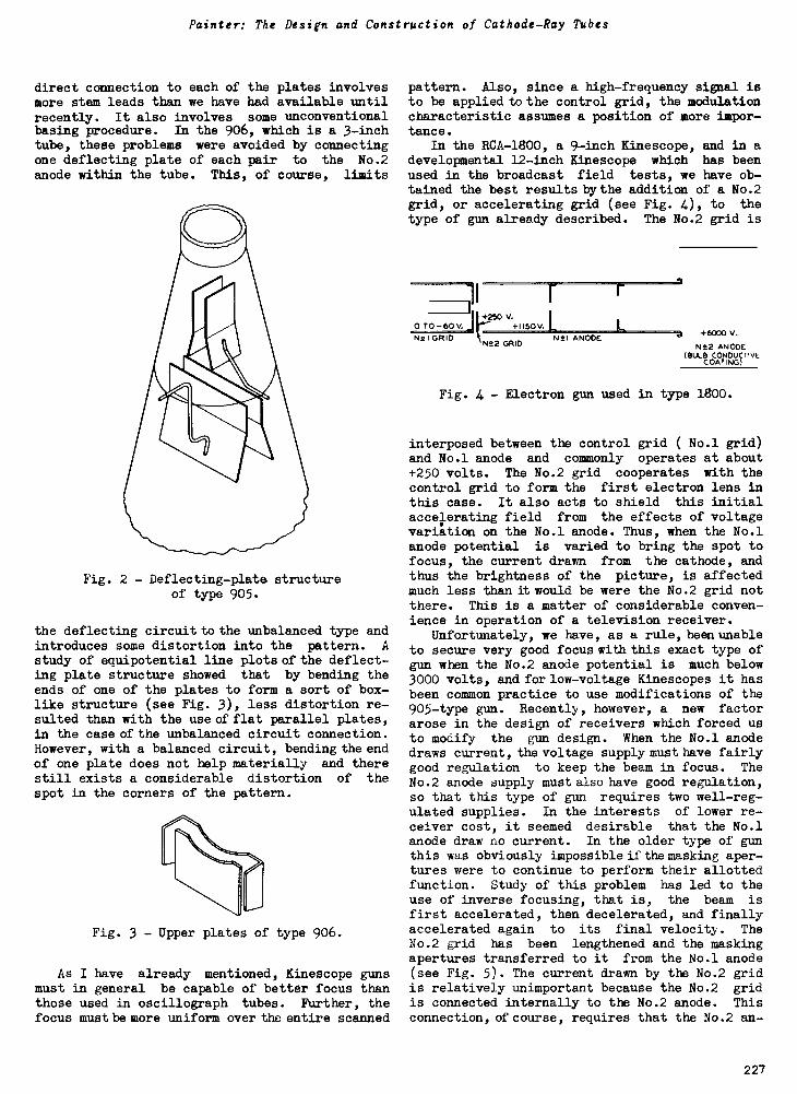
Painter: The Design and Construction of Cathode -Ray Tubes
direct connection to each of the plates involvesmore stem leads than we have had available untilrecently. It also involves some unconventionalbasing procedure. In the 906, which is a 3 -inchtube, these problems were avoided by connectingone deflecting plate of each pair to the No.2anode within the tube. This, of course, limits
Fig. 2 - Deflecting-plata structureof type 905.
the deflecting circuit to the unbalanced type andintroduces some distortion into the pattern. Astudy of equipotential line plots of the deflect-ing plate structure showed that by bending theends of one of the plates to form a sort of box-like structure (see Fig. 3), less distortion re-sulted than with the use of flat parallel plates,in the case of the unbalanced circuit connection.However, with a balanced circuit, bending the endof one plate does not help materially and therestill exists a considerable distortion of thespot in the corners of the pattern.
Fig. 3 - Upper plates of type 906.
As I have already mentioned, Kinescope gunsmust in general be capable of better focus thanthose used in oscillograph tubes. Further, thefocus must be more uniform over the entire scanned
pattern. Also, since a high -frequency signal isto be applied to the control grid, the modulationcharacteristic assumes a position of more impor-tance.
In the RCA -1800, a 9 -inch Kinescope, and in adevelopmental 12 -inch Kinescope which has beenused in the broadcast field tests, we have ob-tained the best results by the addition of a No.2grid, or accelerating grid (see Fig. 4), to thetype of gun already described. The No.2 grid is
1
+25°V.
070-60V. +1150 v. 1.. L
r
Ns I GRIDNe2 GRID
Nil ANODE 4 +6000 v.
N22 ANODE(BULB CONDUCTIVE
COATING)
Fig. 4 - Electron gun used in type 1800.
interposed between the control grid ( No.1 grid)and No.1 anode and commonly operates at about+250 volts. The No.2 grid cooperates with thecontrol grid to form the first electron lens inthis case. It also acts to shield this initialaccelerating field from the effects of voltagevariation on the No.1 anode. Thus, when the No.1anode potential is varied to bring the spot tofocus, the current drawn from the cathode, andthus the brightness of the picture, is affectedmuch less than it would be were the No.2 grid notthere. This is a matter of considerable conven-ience in operation of a television receiver.
Unfortunately, we have, as a rule, been unableto secure very good focus with this exact type ofgun when the No.2 anode potential is much below3000 volts, and for low -voltage Kinescopes it hasbeen common practice to use modifications of the905 -type gun. Recently, however, a new factorarose in the design of receivers which forced usto modify the gun design. When the No.1 anodedraws current, the voltage supply must have fairlygood regulation to keep the beam in focus. TheNo.2 anode supply must also have good regulation,so that this type of gun requires two well -reg-ulated supplies. In the interests of lower re-ceiver cost, it seemed desirable that the No.1anode draw no current. In the older type of gunthis was obviously impossible ifthemasking aper-tures were to continue to perform their allottedfunction. Study of this problem has led to theuse of inverse focusing, that is, the beam is
first accelerated, then decelerated, and finallyaccelerated again to its final velocity. TheNo.2 grid has been lengthened and the maskingapertures transferred to it from the No.1 anode(see Fig. 5). The current drawn by the No.2 gridis relatively unimportant because the No.2 gridis connected internally to the No.2 anode. Thisconnection, of course, requires that the No.2 an -
227
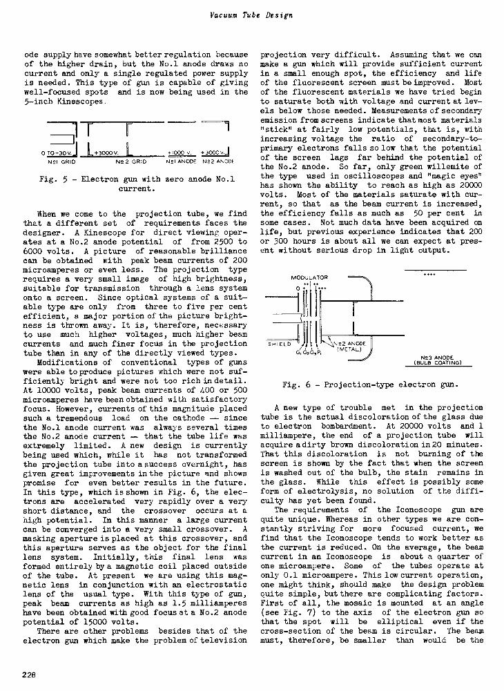
Vacuum Tube Design
0 TO -30 V. L+3000 V.
ode supply have somewhat better regulation becauseof the higher drain, but the No.1 anode draws nocurrent and only a single regulated power supplyis needed. This type of gun is capable of givingwell -focused spots and is now being used in the5 -inch Kinescopes.
r F
LN2I GRID N22 GRID
4-1000 V. -1.3000VA
N2I ANODE N92 ANODE
Fig. 5 - Electron gun with zero anode No.1current.
When we come to the projection tube, we findthat a different set of requirements faces thedesigner. A Kinescope for direct viewing oper-ates at a No.2 anode potential of from 2500 to6000 volts. A picture of reasonable brilliancecan be obtained with peak beam currents of 200microamperes or even less. The projection typerequires a very small image of high brightness,suitable for transmission through a lens systemonto a screen. Since optical systems of a suit-able type are only from three to five per centefficient, a major portion of the picture bright-ness is thrown away. It is, therefore, necessaryto use much higher voltages, much higher beamcurrents and much finer focus in the projectiontube than in any of the directly viewed types.
Modifications of conventional types of gunswere able to produce pictures which were not suf-ficiently bright and were not too rich in detail.At 10000 volts, peak beam currents of 400 or 500microamperes have been obtained with satisfactoryfocus. However, currents of this magnitude placedsuch a tremendous load on the cathode -- sincethe No.1 anode current was always several timesthe No.2 anode current -- that the tube life wasextremely limited. A new design is currentlybeing used which, while it has not transformedthe projection tube into asuccess overnight, hasgiven great improvements in the picture and showspromise for even better results in the future.In this type, which is shown in Fig. 6, the elec-trons are accelerated very rapidly over a veryshort distance, and the crossover occurs at ahigh potential. In this manner a large currentcan be converged into a very small crossover. A
masking aperture is placed at this crossover, andthis aperture serves as the object for the finallens system. Initially, this final lens wasformed entirely bya magnetic coil placed outsideof the tube. At present we are using this mag-netic lens in conjunction with an electrostaticlens of the usual type. With this type of gun,peak beam currents as high as 1.5 milliampereshave been obtained with good focus at a No.2 anodepotential of 15000 volts.
There are other problems besides that of theelectron gun which make the problem of television
projection very difficult. Assuming that we canmake a gun which will provide sufficient currentin a small enough spot, the efficiency and lifeof the fluorescent screen must be improved. Most
of the fluorescent materials we have tried beginto saturate both with voltage and current at lev-els below those needed. Measurements of secondaryemission from screens indicate that most materials"stick" at fairly low potentials, that is, withincreasing voltage the ratio of secondary -to -
primary electrons falls so low that the potentialof the screen lags far behind the potential ofthe No.2 anode. So far, only green willemite ofthe type used in oscilloscopes and "magic eyes"has shown the ability to reach as high as 20000volts. Most of the materials saturate with cur-rent, so that as the beam current is increased,the efficiency falls as much as 50 per cent in
some cases. Not much data have been acquired onlife, but previous experience indicates that 200or 300 hours is about all we can expect at pres-ent without serious drop in light output.
MODULATOR
1
0 4.4...
SHIELDG,G2G,P
N22 ANODE(METAL)
4+4.
N23 ANODE(BULB COATING)
Fig. 6 - Projection -type electron gun.
A new type of trouble met in the projectiontube is the actual discoloration of the glass dueto electron bombardment. At 20000 volts and 1milliampere, the end of a projection tube willacquire adirty brown discoloration in20 minutes.That this discoloration is not burning of thescreen is shown by the fact that when the screenis washed out of the bulb, the stain remains inthe glass. While this effect is possibly someform of electrolysis, no solution of the diffi-culty has yet been found.
The requirements of the Iconoscope gun arequite unique. Whereas in other types we are con-stantly striving for more focused current, wefind that the Iconoscope tends to work better asthe current is reduced. On the average, the beamcurrent in an Iconoscope is about a quarter ofone microampere. Some of the tubes operate atonly 0.1 microampere. This low current operation,one might think, should make the design problemquite simple, but there are complicating factors.First of all, the mosaic is mounted at an angle(see Fig. 7) to the axis of the electron gun sothat the spot will be elliptical even if thecross-section of the beam is circular. The beammust, therefore, be smaller than would be the
228
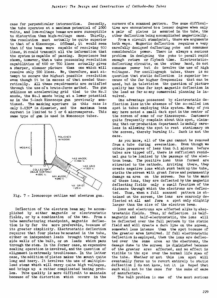
Painter: The Design and Construction of Cathode -Ray Tubes
case for perpendicular intersection. Secondly,the tube operates at a maximum potential of 1000volts, and low -voltage beams are more susceptibleto distortion than high -voltage ones. Thirdly,
the resolution must actually be quite superiorto that of a Kinescope. Offhand, it would seemthat if the beam were capable of resolving 500lines, it could transmit all the information thatthe system is capable of passing. Experience hasshown, however, theta tube possessing resolutioncapabilities of 600 or 700 lines actually givesa sharper, cleaner picture than one which willresolve only 500 lines. We, therefore, must at-tempt to secure the highest possible resolutioneven though it be in excess of that needed theo-retically. All these requirements are satisfiedthrough the use of a brute -force method. The gunutilizes an accelerating grid tied to the No.2anode, the No.1 anode being at a lower potentialas in the 5 -inch Kinescope gun previously men-
tioned. The masking aperture in this case isonly 0.030" in diameter, and the maximum beamcurrent is limited to 5 or 6 microamperes. This
same type of gun is used in Monoscope tubes.
POLISHEDWINDOW
COLLECTOR(BULB COATING)
+1000 V.N21 ANODE
+280 V.
N!2 ANODE+1000 V.
N22 GRID+1000 V.
N21 GRID-25 V.
Fig. 7 - Iconoscope outline and electron gun.
Deflection of the electron beam may be accom-plished by either magnetic or electrostaticfields, or by a combination of the two. From atube manufacturing standpoint, magnetic deflec-tion is by far the more preferable, because ofits greater simplicity. Electrostatic deflectionrequires that four plates be mounted in the tube,either on independent leads brought through theside walls of the bulb, or on leads which passthrough the stem. In the former case, an expensivesealing operation is involved, and the question ofalignment is extremely troublesome. In the lattercase, theadditionofplates makes the mount quitelong and heavy. It involves the use of multiple -lead stems which will carry quite high voltages,and brings up a rather complicated basing prob-lem. Tube quality is more difficult to maintainbecause of the distortion which occurs in the
corners of a scanned pattern. The same difficul-ties are encountered toa lesser degree when onlya pair of plates is mounted in the tube, theother deflection being accomplished magnetically.
From a circuit standpoint, there are argumentsboth ways. Magnetic deflection requires a verycarefully designed deflecting yoke and consumesconsiderable power. There is always a seriousproblem in designing the yoke to permit rapidenough return or flyback time. Electrostatic -
deflecting circuits, on the other hand, do notconsume power but do involve the use of highvoltages. For oscillograph tubes, there is noquestion that static deflection is superior be-cause of the far higher frequencies that can beused, but in television the question of picturequality has thus far kept magnetic deflection inthe lead as far as any commercial planning is in-volved.
One advantage possessed by electrostatic de-flection lies in the absence of the so-called ionspot in tubes employing this system. Many of youmay have noted a small dark spot in the center ofthe screen of some of our Kinescopes. Customersquite frequently complain about this spot, claim-ing that our production department is unduly care-less in allowing the spot to rest stationary onthe screen, thereby burning it. Such is not thecase.
As you know, all of the gas cannot be removedfrom a tube during evacuation. Even though weobtain pressures of less than 0.1 micron beforetubes are tipped off, there is sufficient resid-ual gas to be ionized by the passage of the elec-tron beam. The positive ions thus formed are
attracted to the cathode. Arriving there, theycreate negative ions which rush back up the tube,strike the screen with great force and permanentlydamage an area on the screen. Due to the massof these ions, they are deflected by the magneticdeflecting fields only a small fraction of thedistance through which the electrons are deflec-ted. Thus, when a full scanned pattern is ob-tained on the screen, the ions are scarcely de-flected at all and form a spot only slightlylarger than the size of the electron beam.
Ions and electrons are affected alike by elec-trostatic fields. Thus, if deflection is half -
magnetic and half -electrostatic, the ions willbe deflected over the full pattern by the staticfield and will create a dark line on the screen,somewhat less intense than the spot because ofthe greater area involved. If full electrostaticdeflection is employed, then the ions are deflec-ted over the same area as the electrons, thedamage done to the screen is diminished becauseof the greater area affected, and no effect isvisible to the eye over the normal life span ofthe tube. Whether or not this ion spot willeventually force us to revert entirely to staticdeflection I do not know, but it is hoped thatsuch will not be the case for the sake of easeof manufacture.
The bulb problem is one of the most serious
229
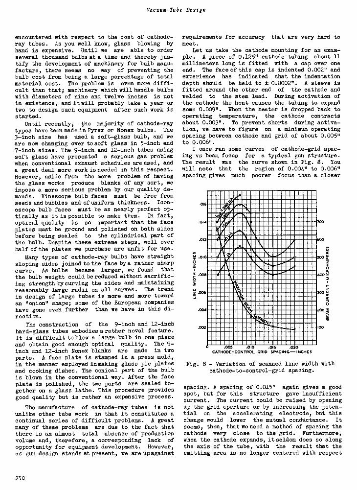
Vacuum Tube Design
encountered with respect to the cost of cathode-ray tubes. As you well know, glass blowing byhand is expensive. Until we are able to orderseveral thousand bulbs at a time and thereby jus-tify the development of machinery for bulb manu-facture, there seems no way of preventing thebulb cost from being a large percentage of totalmaterial cost. The problem is even more diffi-cult than that; machinery which will handle bulbswith diameters of nine and twelve inches is notin existence, and it will probably take a year ortwo to design such equipment after such work isstarted.
Until recently, the majority of cathode-raytypes have been made in Pyrex or Nonex bulbs. The
3 -inch size has used a soft -glass bulb, and weare now changing over to soft glass in 5 -inch and7 -inch sizes. The 9 -inch and 12 -inch tubes usingsoft glass have presented a serious gas problemwhen conventional exhaust schedules are used, anda great deal more work is needed in this respect.However, aside from the mere problem of havingthe glass works produce blanks of any sort, weimpose a more serious problem by our quality de-mands. Kinescope bulb faces must be free fromseeds and bubbles and of uniform thickness. Icon-
oscope bulb faces must be as nearly perfect op-tically as it is possible to make them. In fact,
optical quality is so important that the faceplates must be ground and polished on both sidesbefore being sealed to the cylindrical part ofthe bulb. Despite these extreme steps, well overhalf of the plates we purchase are unfit for use.
Many types of cathode-ray bulbs have straightsloping sides joined to the face bya rather sharp
curve. As bulbs became larger, we found that
the bulb weight could be reduced without sacrific-ing strength by curving the sides and maintainingreasonably large radii on all curves. The trendin design of large tubes is more and more towardan "onion" shape; some of the European companieshave gone even further than we have in this di-
rection.
The construction of the 9 -inch and 12 -inch
hard -glass tubes embodies arather novel feature.It is difficult to blow a large bulb in one pieceand obtain good enough optical quality. The 9 -
inch and 12 -inch Nonex blanks are made in two
parts. A face plate is stamped in a press mold,in the manner employed in making glass pie platesand cooking dishes. The conical part of the bulbis blown in the conventional way. After the faceplate is polished, the two parts are sealed to-gether on a glass lathe. This procedure providesgood quality but is rather an expensive process.
The manufacture of cathode-ray tubes is notunlike other tube work in that it constitutes acontinual series of difficult problems. A greatmany of these problems are due to the fact thatthere is an almost total absence of productionvolume and, therefore, a corresponding lack of
opportunity for equipment development. However,as gun design stands at present, we are up against
requirements for accuracy that are very hard tomeet.
Let us take the cathode mounting for an exam-ple. A piece of 0.125" cathode tubing about 11millimeters long is fitted with a cap over oneend. The face of this cap is indented 0.002" andexperience has indicated that the indentationdepth should be held to ± 0.0002". A sleeve isfitted around the other end of the cathode andwelded to the stem lead. During activation ofthe cathode the heat causes the tubing to expandsome 0.009". When the heater is dropped back tooperating temperature, the cathode contractsabout 0.003". To prevent shorts during activa-tion, we have to figure on a minimum operatingspacing between cathode and grid of about 0.005"to 0.006".
I once ran some curves of cathode -grid spac-ing vs beam focus for a typical gun structure.The result was the curve shown in Fig. 8. Youwill note that the region of 0.004" to 0.006"spacing gives much poorer focus than a closer
.016
.014
.012
ta .010
.00sa
Z .006
.004
700
600
500 12
0
40002
z300 w
Cc
4.)
200 2
.002 100
005 0 0 0 5 020CATHODE-CONTROL GRID SPACING-INCHES
Fig. 8 - Variation of scanned line width withcathode -to -control -grid spacing.
spacing. A spacing of 0.015" again gives a goodspot, but for this structure gave insufficientcurrent. The current could be raised by openingup the grid aperture or by increasing the poten-tial on the accelerating electrode, but thischange would lower the mutual conductance. It
seems, then, that we need a method of spacing thecathode very close to the grid. Furthermore,when the cathode expands, it seldom does so alongthe axis of the tube, with the result that theemitting area is no longer centered with respect
230
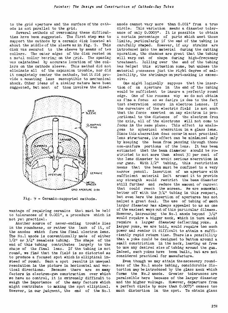
Painter: The Design and Construction of Cathode-Ray Tubes
to the grid aperture and the surface of the cath-ode is not parallel to the grid.
Several methods of overcoming these difficul-ties have been suggested. The first step was tosupport the cathode by a ceramic disk located atabout the middle of the sleeve as in Fig. 9. This
disk was secured to the sleeve by means of twocollars. The outer edges of the disk rested ona metal collar bearing on the grid. The spacingwas maintained by accurate location of the col-lars on the cathode sleeve. This method did noteliminate all of the expansion trouble, nor didit completely center the cathode, but it did pro-vide a mounting less susceptible to mechanicalshock. Other ideas of a similar nature have beensuggested, but most of them involve the disad-
CATHODE.
SUPPORTS
.11
11
APERTURE
GRID^." SLEEVE
CLAMPING--- RING
CERAM IC
METALSPACER
GRID APERTURE DISK
Fig. 9 - Ceramic -supported cathode.
vantage of requiring ceramics that must be heldto tolerances of ± 0.001", a procedure which isnot yet practical.
Another source of never-ending trouble liesin the roundness, or rather the lack of it, ofthe anodes which form the final electron lens.The No.1 anode is conventionally made of either1/2" or 3/4" seamless tubing. The shape of theend of this tubing contributes largely to theshape of the final lens. If the tubing is notround, we find that the field is so distorted asto produce a focused spot which is elliptical in-stead of round. Such a spot results in unequalresolution in the picture in horizontal and ver-tical directions. Because there are so manyfactors in electron -gun construction over whichwe have no control, it is extremely difficult toweigh the importance of the many factors whichmight contribute to making the spot elliptical.However, in our judgment, the end of the No.1
anode cannot vary more than 0.001" from a truecircle. This variation means a diameter toler-ance of only 0.0005". It is possible to obtaina certain percentage of parts which meet theselimits, particularly if the end of the tubing iscarefully shaped. However, if any strains areintroduced into the material during the cuttingoperation, the chances are great that the tubingwill warp out of shape during high -frequencytreatment. Rolling over the end of the tubinghas helped this situation some, but unless thematerial possesses just the right degree of mal-leability, the shrinkage on part -making is exces-sive.
One might logically suppose that the inser-tion of an aperture in the end of the tubingwould be sufficient to insure a perfectly roundedge. One of the reasons why we do not obtainas fine a focus as we desire is due to the factthat aberration occurs in electron lenses. If
the curvature of the electric field is not suchthat the force exerted on any electron is pro-portional to the distance of the electron fromthe axis, all of the electrons will not come tofocus in the same plane. This effect is analo-gous to spherical aberration in a glass lens.Since this aberration does occur in most practicallens structures, its effect can be minimized onlyby keeping the beam from passing through thosenon -uniform portions of the lens. It has beenestimated that the beam diameter should be re-stricted to not more than about 30 per cent of
the lens diameter to avoid serious aberration inour guns. With 1/2" tubing, this restrictionmeans that the beam must be confined to a verynarrow pencil. Insertion of an aperture withsufficient material left around it to provideany strength would restrict the beam diameterstill further and reduce the amount of currentthat could reach the screen. We are somewhatbetter off with the 3/4" tubing in this respect,but even here the insertion of apertures has nothelped a great deal. The use of tubing of muchlarger diameter has always appealed to us as oneof the easiest ways out of this particular dilemma.However, increasing the No.1 anode beyond 3/4"would require a bigger neck, which in turn wouldrequire a larger diameter deflecting yoke. Alarger yoke, we are told, would require too muchpower and render it difficult to attain a suffi-ciently rapid return time. There is a possibilitythat a yoke could be designed to button around asmall constriction in the neck, leaving us freeto use any desired size of tubing around the gun.Indeed, such yokes have been built, but are notconsidered practical for manufacture.
Even though we may attain the necessary round-ness of the No.1 anode tubing, considerable dis-tortion may be introduced by the glass neck whichforms the No.2 anode. Greater tolerances arepermissible here because of the larger diameterand the higher voltage. However, departure froma perfect circle by more than 0.0075" causes toomuch distortion in the spot. To obtain glass
231
Vacuum Tube Design
tubing within such a limit is extremely costly.The logical solution for a No.2 anode seems tobe to use a metallic cylinder supported by themount. With this construction, however, we runinto the problem of mounting insulation that willstand a potential difference of about 5000 voltswithout having objectionable leakage.
Since cathode-ray beams are quite susceptibleto magnetic fields, it is essential that we usea non-magnetic material for our mount parts. It
has been common practice in the past to use Monel,but we are trying to find an acceptable substi-tute. Too many lots of Monel are received whichcan be picked up with a magnet. Then, too, wefrequently find that the material has acquiredmagnetic properties after it has undergone heattreatment. Nichrome has always been very satis-factory from a magnetic standpoint, but the mater-ial cannot be obtained in seamless tubing. At
the present time, we are working with stainlesssteel and Inconel as the most likely substitutes.
Assuming for the moment that we have obtaineda perfect cathode mounting, a perfectly roundanode of non-magnetic material, and a perfectlyround tube neck, we probably still would be ableto turn out a sizable quantity of rejects becauseof poor mount alignment. As you noted earlierin the discussion, there may be from two to fiveor six apertures along the axis of the gun. Thesemust be co -axial to within ± 0.001" if the focusis to be good. In the past we have dependedlargely upon mandrels projecting through theseapertures to line them up. This procedure imme-diately imposes the limitation that the aperturesizes must all be the same or decrease as we pro-gress toward the grid. Furthermore, when it is
considered that 0.040" is a fairly common sizeand even 0.030" is found in some tubes, the main-tenance problem on such slim mandrels can be ap-preciated. On low -voltage oscillograph tubes,
where there is considerable tolerance on focus,we have adopted a ceramic mounting. The anodesare made of two formed halves and are welded to-gether around two supporting ceramic rods. This
arrangement appears to work successfully in the913 and the new 902, but for tubes with highervoltage ratings there is a serious problem ofleakage across the ceramic rods. To date, noneof the results from this type of gun have givenany indication that television quality could bemaintained by this process. Our television tubes,as a result, still utilize a glass -bead type of
mount. This differs from the conventional typein that, instead of using pre -formed beads, weweld all the supports to the various parts, sup-port the assembly in a jig, and melt the glassdown over the supports. This procedure preventsstrains set up during welding from destroying thealignment when the mandrel is removed, but itdoes set up strains and warping during heating ofthe anodes and oxidizes the parts so that theirappearance is poor.
On the projection -tube mount, we are forcedto use a different technique. Here the mount
consists of a series of apertures with no connect-ing tubing. Six apertures may be mounted in atotal length of not over 3/4", the final aperturerunning at 6000 volts or over. Since the aper-ture in the final disk is only 0.004" diameter,the use of a mandrel is impossible. Instead, wetry to hold very close tolerances on the outsidediameter of the aperture disks and on the center-ing of the holes. The disks are then droppedinto a V-shaped block and alignment depends uponthe accuracy of the parts.
Exhaust of cathode-ray tubes until very re-cently has been done entirely on trolley posi-tions. During the past two years, however, con-siderable progress has been made in the develop-ment of a machine. At present we have two suchmachines, one for 2 -inch and 3 -inch tubes, andone for 5-, 7-, 9-, and 12 -inch types. Theydiffer from conventional sealex machines chieflyin the size of sweeps used and in the slower in-dexing speed. Because of the extremely high vac-uum needed, we have found it necessary to mountthe mercury pumps on the turret and provide apump for each port. The speed has been graduallyincreased until we can pump 3 -inch oscillographtubes at the rate of 60 per hour. Televisiontubes can be pumped in from 20 minutes to 1 hourper revolution of the machine, depending on thepermissible baking temperature, the size of thebulb, and the type of fluorescent -screen mater-ial used. A baking oven is mounted over thetrack for the first six positions. Mr. Kaufmanndealt quite completely with the subject of screenmaterials in Lecture 5, so I will mention themonly briefly. As you know, the most common typeof screen is the so-called green willemite, whichis zinc orthosilicate. The silicate screen mater-ials are quite stable and easily handled and pre-sent no serious problems on exhaust. When thedemand for a white screen for television arose,a great deal of work was done with mixtures ofblue and yellow zinc sulfides. The yellow sul-fide in particular was quite unstable and verydifficult to handle in production. If the bakingtemperature was raised above 35000, the screenwas likely to assume any one of a number of un-desirable shades. On the other hand, if the
temperature was kept below 42500, the tubes gen-erally failed in five or ten hours because ofgas. One possible solution involves the use ofa mixture of blue sulfide and yellow silicatematerial. To date, this mixture seems to havemost of the desirable characteristics of the sil-icate materials. Machine exhaust seems quitefeasible and the chief problems are to developfurther the process of making blue sulfide andto maintain sufficient purity in the processing.Extremely minute quantities of copper are suffi-cient to cause changes in the color of the screens;and the entire processing of the tubes must befree of any contamination. Both of these prob-lems can be solved, we feel, and the white mater-ial is expected to become standard on televisiontubes before long.
232
Painter: The Design and Construction of Cathode -Ray Tubes
There remains to be said a brief word abouttesting cathode-ray tubes. In addition to manyof the electrical characteristics which are meas-ured on receiving tubes, we are interested in
the questions of focus and brilliance. We firsttry to determine "optimum conditions". Thesemight be defined as those conditions which willgive us the brightest possible picture of therequired resolution. Resolution can, of course,be determined by measuring the size of the focusedspot. However, any appreciable amount of currentin a stationary spot would damage the screen ir-reparably, so that it is necessary to apply scan-ning voltages and measure the width of the scannedline by the use of a calibrated telescope. The
widest line that will give the required resolu-tion is chosen depending on the size of the tube.The grid bias is then increased until the scannedline becomes the predetermined width and the con-ditions of bias and focusing voltages are noted.Herein lies the first inaccuracy in the testingmethod. It has been shown that the distributionof electron density across the width of a scannedline is approximately Maxwellian in nature. The
light derived from a fluorescent screen dependsupon the number of electrons striking the screen.As the spot is scanned across the screen, it isobvious that any unit area traversed by the cen-ter of the spot will be bombarded by more elec-trons than a similar area near the edge of thespot. As a result the brightness of a line de-creases from the center to the edge. When viewedthrough a telescope with a magnification of some50 times, the edge of the line is very indis-tinct, and the judgment of the operator entersinto the reading. Furthermore, if the spot iselliptical and the long axis of the ellipse coin-cides with the direction of scanning, an optimis-tic reading will result.
Since the apparent line width varies with thevelocity of scanning, it has been considered nec-essary to scan the screen during testing with avelocity comparable to that of a television pic-ture. Circuits generating saw -tooth voltages atabout 13000 cycles per second are rather temper-amental and are not suited to factory usage. In-stead, we use a sine -wave scanning voltage of amuch lower frequency and adjust the length ofthe scanned line so that the velocity of the spotat the center of the screen is the same as that
achieved with the higher -frequency saw -tooth
voltage. Sine -wave scanning offers another ad-vantage. Since the spot must slow down and re-verse its direction, the intensity of the endsof the lines is higher than elsewhere. The brightspot thus formed at the end of each line hasvirtually the same appearance as a stationaryspot. By looking at the end of a line, the oper-ator can judge the ellipticity of the spot. Spec-ifications call for adjusting the focus, not forthe narrowest line, but for that condition in
which the spot at the end of a line has the mostnearly symmetrical appearance -- again a matterof judgment. In some types of television tubes,we have been focusing for the narrowest horizon-tal line, then rotating the yoke 90 degrees andmeasuring the line width in the vertical direc-tion. The height and width of the spot, plusthe width of the line under symmetrical condi-tions, gives us a measure of the resolution cap-abilities of the tube. Testing in this way isexpensive and not satisfactory for production.
Having measured resolution, we must then testthe performance of the fluorescent screen. Form-erly, we required two light measurements; now wemeasure only once and calculate the other reading.The beam current is reduced to 50 microamperes,and the pattern size reduced to a standard area,usually 6 x 8 centimeters. The light output ismeasured from this pattern, and the screen effi-ciency calculated in terms of candlepower outputper watt input to the screen. In the factory thisreading is taken by means of a photronic cellwhose output is measured on a light -beam galva-nometer. The cell is first placed over the scannedpattern, and the meter reading noted. The cellis then placed over a ground -glass plate behindwhich is mounted a calibrated lamp on a movablesocket. The distance from the lamp to the screenis varied until the cell shows the same readingon the meter as before. The light output is thendetermined from a chart showing light output vsdistance of the lamp from the screen. This equip-ment requires frequent calibration, but in gen-eral is considerably more satisfactory than theilluminometer used by the laboratory. Some sortof light reading will probably have to be takenuntil that far-off day when we can depend uponthe uniformity of fluorescent materials to a muchgreater extent than we can to -day.
233
Lecture 25
ELECTRON BEAMS AND THEIR APPLICATION IN RADIO TUBES
H. M. Wagner
BEAM TUBE DEFINED
The term "beam tube," as used here, covers a
wide variety of devices. The term is sufficientlynew so that it does not yet have a generally ac-cepted meaning. Of the many different tube typesmanufactured by RCA, only the "Beam Power Tubes,"such as the 6L6, 25L6, and 807, are cataloguedwith the "beam" designation. Other types, whichare beam tubes, are the many cathode-ray tubesand the "Magic Eye" types 6E5, 6G5, 6N5, 6U5, and6AF6-G.
A tentative definition' of "Electron BeamTube" has been proposed as follows: "An electronbeam tube is a vacuum tube providing a directedflow of charged particles substantially in theform of a beam or beams and in which the beamformation contributes materially to the perform-ance characteristics."
It is not enough, therefore, to classify atube as a beam tube because its space current issegregated into beams, except when some new orimproved performance is achieved by means of thebeam formation. Among the tube types alreadycited, the beam power tubes depend on the segre-gation of the electrons into beams between thegrid wires without deflection of the beams. The
cathode-ray and magic -eye tubes depend on theproperties of focusing and deflection of electronbeams.
METHODS OF STUDYING BEAM FORMATIONAND PROPERTIES
Information on electron paths is an essentialpart of the design of beam tubes. These pathscan be found and studied using the followingmethods.
A. Without Building Tube
I) Graphical Method Using Electric -Field Plot
In this method a plot is made of equipo-tential lines throughout a cross-section repre-senting the actual tube. An electrolytic tankis commonly employed. Metal parts are shapedsimilar to the electrodes of the tube and areplaced in a tank of slightly conducting electro-lyte, such as drinking water, to form an enlargedsection of the tube. The parts are connected topotentials proportional to the voltages to beused on the tube electrodes and a movable probedipping into the electrolyte takes the potential
1 Proposed by Subcommittee on Electron Beam Tubesof the I.R.E. Technical Committee on Electronics,November, 1937.
at any point. By having a null voltage indicat-ing device between the probe and an adjustablevoltage source, the probe can be guided alonglines of constant voltage and the equipotentiallines plotted. The equipotential plots in Figs.2 to 7 were made by the above method.
The path of an electron can then be plot-ted from the electric -field plot by various meansinvolving subdivision of the path into a numberof short straight lines approximating the truecurved path.
This method is laborious and requires con-siderable time for plotting the many possiblepaths of electrons emerging from different partsof the cathode and having different initial vel-ocities. Initial velocities can be disregardedin many cases.
2) Rubber -Membrane Potential Contour
Parts representing a cross-section of thetube are made out of wood or other material. Theseare mounted with their plane surfaces at depthsbelow the cathode plane proportional to the cor-responding tube -electrode voltages to cathode.An electrode at negative voltage, such as a biasedgrid, is higher than the cathode. A thin rubbersheet uniformly stretched by a frame is held overthe parts so that it presses against all the sur-faces. It can be shown that a thin flexible elas-tic membrane held under uniform tension andplaced in this way over parts having relativelysmall differences in elevation between them has atopographical surface the same as that of theelectric field in the tube and that the path ofa ball allowed to roll from the cathode is the
same as that taken by an electron in the tube.Initial velocities of electrons are simulated bystarting velocities of the balls. The electrontrajectories are determined by observation orphotographing the paths of the balls.
2) Langmuir Automatic Electron -Path Plotter
The radius of curvature of an electron mov-ing in an electric field can be shown to be equalto
2 (V + Vo)
dV
dr
where V is the electric potential in space; Vo,the initial velocity with which the electron en-ters the electric field; and dV/dr, the electricgradient normal to its direction of motion. In
Langmuir's apparatus,2 a double -pointed probe
2 D. B. Langmuir, "Nature," Vol. 139, p. 1066;June 19, 1937.
234
Wagner: Electron Beams and their Application in Radio Tubes
dips into an electrolytic tank holding electrodesrepresenting the tube cross-section. The smalldifference of potential between the points of theprobe, which are close together and insulated,gives the potential gradient, while, simultane-ously, the voltage on them gives the electric po-tential. The probe is supported by a motor -drivencarriage, the wheels of which are steered by avacuum -tube -controlled electric motor that makesthe carriage move in a path having a radius ofcurvature proportional to the ratio of the volt-ages on and between the points of the probe. Thecarriage and probe thus trace the electron path.A plot is made by a pencil attached to the car-riage.
The three foregoing methods of plottingelectron paths without building a tube are ofconsiderable value in beam -tube design, althoughtheir application is limited. One limitation isthe neglect of electron space charge, which isimportant in many instances. The class of tubesin which a magnetic field influences or controlsthe electron paths cannot be studied by thismeans. Because of the geometrical form of manytubes, the electron paths cannot be found or elsethey can be determined only for certain cross -sections through the tube. Specifically, theelectron paths which can be determined are thosewhich lie in a plane surfaced and the cross-section through the tube must be chosen so thatthis plane cuts no equipotential lines, i.e., theequipotential lines must be completely containedin the plane.
As an example showing the geometrical lim-itations of the methods, consider electron pathsin a triode, such as the RCA -56, having a cylin-drical cathode and anode and a helical -wound grid.The helical grid does not permit a plane to bepassed which does not intersect lines of force.As an approximation, a ring -type grid can be as-sumed and substituted. Then there are threeplanes that can be passed which satisfy the re-quirements, i.e., one perpendicular to the cath-ode and halfway between grid rings, one parallelto and through the axis of the cathode and gridside -rods, and another through the cathode axisand at right angles to the plane through the gridside -rods. Electron focusing between grid wiresoccurs in the latter plane and can be examined bymaking a model of half of the tube and immersingit in the electrolytic tank so that the planethrough the model is at the surface of the liquid.But, placing the rubber membrane over the straightedges of the cathode and anode pieces and thecircular cross-section grid wires simulates andshows the grid -control action of a parallel -plane
3 It is conceivable that the electrolytic -tank orLangmuir method with a submerging probe (three -pointed in the Langmuir method) could be adaptedto plot paths in three dimensions, but the designand constructional difficulties involved mighteasily make this adaptation impractical.
structure instead of the cylindrical tube. Ingeneral, the geometrical configurations suitablefor the rubber membrane are more limited than forthe electrolytic tank and must not only have across --sectional area containing a two-dimensional
electric field but they are also limited to two-dimensional mechanical symmetry, i.e., they musthave the same cross-section throughout the length.
B. By Visual Observations on Actual Tubes
1) Tubes Containing Small glpantity of Gas
The presence of a small quantity of gasmakes visible the region of electron flow andshows the outline of the beam. The quantity ofgas needed to make the beam distinctly visibleand hence the change in electron paths from goodvacuum conditions, depends among other thingsupon the depth of the beam cross-section lookedthrough. The greater the depth of beam, thesmaller the gas pressure required. In observa-tions on various beam tubes having willemite-coated electrodes, H. C. Thompson found that gascan be introduced in the tube in quantity suffi-cient to give a glow without causing observablechange in the luminescent traces on the willemite.It would appear, therefore, that the electronpath can be only slightly different than in vac-uum.
The gas can be introduced into the bulb byheating the tube parts, by not flashing the get-ter, or by the introduction of specific gases incontrolled quantities on an exhaust system.
2) Tubes with Solid Metal or Tran!parent MetalElectrodes Coated with willemite
While the glow in gas is throughout thebeam, it is often sufficient to know the size andshape of the beam cross-section along the path,for example, where the beam strikes an outputelectrode or passes through an aperture. Willem-ite-coated parts at the desired places in thetube and operating at appropriate voltages showthe luminescent beam traces. In some tubes cer-tain parts have been made movable in order toobserve the beam traces for different electrodepositions. The best location of an electrode forsharp focus has been determined in this way.
A technique of utilizing willemite for ob-servation and study of electron beams was devel-oped and used extensively by H. C. Thompson inhis research work on beam tubes.4 It consistsof coating the electrodes (the plate, screengrid, etc.) with a very thin coating of willemitelike that used on the target of the magic -eye
tubes, in contrast to the thick layer applied incathode-ray tubes. It is important that the
4 H. C. Thompson, "Electron Beams and Their Ap-plicationsin Low Voltage Devices," Proc. I.R.E.,Vol. 24, No.10, pp. 1276-1297; October, 1936.
235
Vacuum Tube Design
willemite be coated thin, particularly on elec-trodes operating at low or medium voltages whichare commonly used in radio tubes, because wille-mite is an insulator and unless it is in a thinfilm the voltage drop due to electrons striking
and passing through the willemite can be appre-ciable, and hence the potential on the coatedelectrode is different from that on an uncoatedone. In the early manufacture of the magic eye,some targets were too thickly coated with the re-sult that in some tubes the target was completelydark while others were dark only in parts or spotswhere the resistance between the willemite andthe target was sufficient to drop the potentialto a voltage below the visible threshold. Theelectrodes in many of H. C. Thompson's tubes havebeen made of sheet metal on which parallel milli-meter -spaced lines were marked, and thus have theappearance of graph paper when there are two setsof lines at right angles. Measurements of beamwidth and deflection are relatively easy withtubes having coordinate -marked, willemite-coatedelectrodes. The beam is measured by the coordi-nate lines and can be seen directly or with theaid of a microscope.
Transparent metal films can be coated withwillemite and used as electrodes. Their advan-tage over solid metal electrodes is that the lu-minescent traces are visible from either side.The metal film, when it is thin enough to betransparent, has a moderately high electrical re-sistance so that there is a voltage drop alongits surface due to the beam current. This poten-tial difference can be small. Various tuningindicator tubes which I have made use targets inthe form of a clear mica disc coated with a filmof metal and willemite over the metal. Electri-cal and mechanical contact is made to the discaround its circumference. In this particular
application of transparent films, the maximumvoltage drop along the target for a few milli-amperes beam current need not exceed ten volts.
2) Incandescence of Thin Metal Foil
A sheet of thin metal can be heated to in-candescence in areas bombarded by an intense beamof electrons. Due to thermal conductivity alongthe metal sheet, the incandescence is not confinedto the bombarded area but extenls beyond it somedistance depending on the thickness of the metal.I have tried tantalum foil as thin as one micron.Even foil as thin as this is inadequate wheregood beam resolution is needed, although it is
good enough for some purposes.
asis
4) Incandescence of Wire Mesh, Screen_,_or Helix
Surfaces other than thin foil can be usedincandescent beam -trace indicators. Wire meshone possibility. A row of closely spaced
parallel wires5 will show the spread or deflec-tion of a beam from wire to wire. Each wire
lights up as the beam passes over it. The heatconductivity between wires is substantially zerobut there is some heat radiation. A fine wirehelix, such as a lamp filament, will serve as anindicator. The twisting of the wire into thehelical shape provides an increased length ofpath through which the heat must travel.
j) Incandescence of Soot on Electrodes
Soot deposited from a flame has a loosetexture and is a poor heat conductor. This ther-mal insulating property makes it excellent as anincandescent indicator. Observations on an RCA -56triode having a sooted anode give some quantita-tive idea of the efficacy of the surface. Theparts in this tube are standard except that thecarbonized nickel anode was held in a candle flameso as to coat its interior with a layer of soot.The soot adheres well to the carbonized metalbase. During evacuation the anode was heated ashot as possible to degas the soot. I have observedthe beam traces on the anode for various condi-tions including focus. At focus there are brightlines on the anode opposite the spaces betweengrid -wire turns, the lines and grid turns spaced37.5 to the inch. The incandescent lines standout sharp and distinct, their width being small(approximately 0.005") compared with the 0.027"spacing between them. The very abrupt changefrom light to dark at the boundary of the elec-tron beam on soot is far superior to the beamtraces on tantalum foil having a thickness ofonly one micron. The bombarded area of the sootmay be intensely bright while the remaining sur-face and the exterior of the anode are dark.
Sooteduld other incandescent surfaces havea sphere of usefulness in beam tubes somewhatdifferent from that of willemite. Whereas theillumination from a willemite surface is approxi-mately proportional to the beam density, thebrightness of an incandescent screen varies muchmore steeply and shows high contrast between por-tions of the beam of slightly different intensity.Data from the tables by Jones and Langmuir6 onthe characteristics of tungsten are plotted inFig. 1 and show this change. At a temperatureof 1100°K, the tungsten receives and radiates1.027 watts per sq cm and has a light output of0.00107 candles. When the power input to thescreen, and hence the electron -beam density, isdoubled, there is a 12 -fold increase of bright-ness. High contrast is advantageous for examin-
5 M. Knoll, "Zeitschrift fiir Technische Physik,"Vol. 15, No.12, pp. 584-591; 1934.
6 Dr. Howard A. Jones and Dr. Irving Langmuir,
"The Characteristics of Tungsten Filaments asFunctions of Temperature," G. E. Review, Vol. 30,Nos.6, 7, and 8; 1927.
236
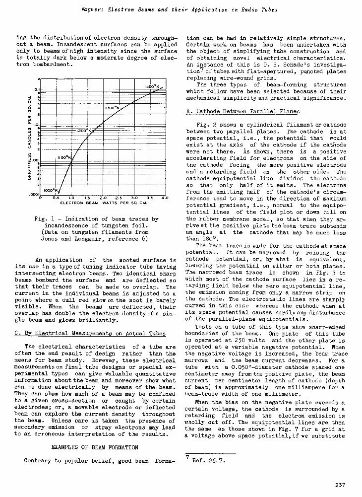
Wagner: Electron Beams and their Application in Radio Tubes
ing the distribution of electron density through-out a beam. Incandescent surfaces can be appliedonly to beams of high intensity since the surfaceis totally dark below a moderate degree of elec-tron bombardment.
O
0a0
Iz
0z
0
0
2
I
I400*K
654
1300°K.3
2
1200.K6543
2
li1100.K.
66543
2
I000*K.,i
0 0.5 I 0 15 2.0 2 5 3.0 3.5ELECTRON BEAM WATTS PER SQ.CM.
Fig. 1 - Indication of beam traces byincandescence of tungsten foil.(Data on tungsten filaments fromJones and Langmuir, reference 6)
4 0
An application of the sooted surface isits use in a type of tuning indicator tube havingintersecting electron beams. Two identical sharpbeams bombard the surface and are deflected sothat their traces can be made to overlap. Thecurrent in the individual beams is adjusted to apoint where a dull red glow on the soot is barelyvisible. When the beams are deflected, theiroverlap has double the electron density of a sin-gle beam and glows brilliantly.
C. By Electrical Measurements on Actual Tubes
The electrical characteristics of a tube areoften the end result of design rather than themeans for beam study. However, these electricalmeasurements on final tube designs or special ex-perimental types can give valuable quantitativeinformation about the beam and moreover show whatcan be done electrically by means of the beam.They can show how much of a beam may be confinedto a given cross-section or caught by certainelectrodes; or, a movable electrode or deflectedbeam can explore the current density throughoutthe beam. Unless care is taken the presence ofsecondary emission or stray electrons may leadto an erroneous interpretation of the results.
EXAMPLES OF BEAM FORMATION
tion can be had in relatively simple structures.Certain work on beams has been undertaken withthe object of simplifying tube construction andof obtaining novel electrical characteristics.An instance of this is O. H. Schade's investiga-tion7 of tubes with flat-apertured, punched platesreplacing wire -wound grids.
The three types of beam -forming structureswhich follow have been selected because of theirmechanical simplicity and practical significance.
A. Cathode Between Parallel Planes
Fig. 2 shows a cylindrical filament or cathodebetween two parallel plates. The cathode is atspace potential, i.e., the potentiil that wouldexist at the axis of the cathode if the cathodewere not there. As shown, there is a positiveaccelerating field for electrons on the side ofthe cathode facing the more positive electrodeand a retarding field on the other side. Thecathode equipotential line divides the cathodeso that only half of it emits. The electronsfrom the emitting half of the cathode's circum-ference tend to move in the direction of maximumpotential gradient, i.e., normal to the equipo-tential lines of the field plot or down hill onthe rubber membrane model, so that when they ar-rive at the positive plate the beam trace subtendsan angle at the cathode that may be much lessthan 180°.
The beam trace is wide for the cathode at spacepotential. It can be narrowed by raising thecathode potential, or, by what is equivalent,lowering the potential on either or both plates.The narrowed beam trace is shown in Fig. 3 inwhich most of the cathode surface lies in a re-tarding field below the zero equipotential line,the emission coming from only a narrow strip onthe cathode. The electrostatic lines are sharplycurved in this case whereas the cathode when atits space potential causes hardly any disturbanceof the parallel -plane equipotentials.
Tests on a tube of this type show sharp -edgedboundaries of the beam. One plate of this tubeis operated at 250 volts and the other plate isoperated at a variable negative potential. Whenthe negative voltage is increased, the beam tracenarrows and the beam current decreases. For atube with a 0.050" -diameter cathode spaced onecentimeter away from the positive plate, the beamcurrent per centimeter length of cathode (depthof beam) is approximately one milliampere for abeam -trace width of one millimeter.
When the bias on the negative plate exceeds acertain voltage, the cathode is surrounded by aretarding field and the electron emission iswholly cut off. The equipotential lines are thenthe same as those shown in Fig. 7 for a grid ata voltage above space potential, if we substitute
Contrary to popular belief, good beam forma-7
Ref. 25-7.
237
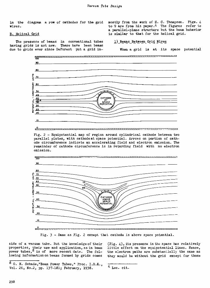
Vacuum Tube Design
in thewires.
B. Helical Grid
The presence of beams in conventional tubeshaving grids is not new. There have been beamsdue to grids ever since DeForest put a grid in -
diagram a row of cathodes for the grid mostly from the work of H. C. Thompson. Figs. 4
to 9 are from his paper.4 The figures refer toa parallel -plane structure but the beam behavioris similar to that for the helical grid.
1) Beams Between Grid Wires
When a grid is at its space potential
100
90
80
ai 50cc
2.5
Z 301.41
20
10
CATHODEAT
SPACEPOTENTIAL
0
Fig. 2 - Equipotential map of region around cylindrical cathode between twoparallel plates, with cathode at space potential. Arrows on portion of cath-ode circumference indicate an accelerating field and electron emission. Theremainder of cathode circumference is in retarding field with no electronemission.
P1 ,/, ,/,/90
80
10
0
Fig. 3 - Same as Fig. 2 except that cathode is above space potential.
side of a vacuum tube. But the knowledge of theirproperties, their use and application, as in beampower tubes,8 is of more recent date. The fol-lowing information on beams formed by grids comes
(Fig. 4), its presence in the space has relativelylittle effect on the equipotential lines. Hence,the electron paths are substantially the same asthey would be without the grid except for those
8 0. H. Schade,"Beam Power Tubes," Proc.Vol. 26, No.2, pp. 137-181; February, 1938. ' Loc. cit.
238
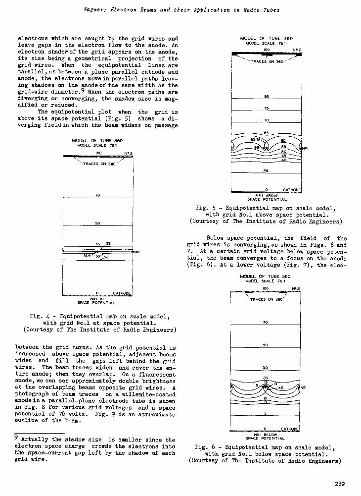
Wagner: Electron Beams and their Application in Radio Tubes
electrons which are caught by the grid wires andleave gaps in the electron flow to the anode. Anelectron shadow of the grid appears on the anode,its size being a geometrical projection of thegrid wires. When the equipotential lines areparallel, as between a plane parallel cathode andanode, the electrons move in parallel paths leav-ing shadows on the anode of the same width as thegrid -wire diameter.9 When the electron paths arediverging or converging, the shadow size is mag-nified or reduced.
The equipotential plot when the grid isabove its space potential (Fig. 5) shows a di-verging field in which the beam widens on passage
MODEL OF TUBE 360MODEL SCALE 751
100 N92
'NNTRACES ON 3607'
70
50
35 i33
N91
MODEL OF TUBE 360MODEL SCALE 75:1
*0 Net
TRACES ON 360
80
75
70
65
63.75 60
6' A 55
,.----------------------------"--.-..)4540
25
0 CATHODE
N21 ABOVESPACE POTENTIAL
NeI
Fig. 5 - Equipotential map on scale model,with grid No.1 above space potential.
(Courtesy of The Institute of Radio Engineers)
Below space potential, the field of thegrid wires is converging, as shown in Figs. 6 and7. At a certain grid voltage below space poten-tial, the beam converges to a focus on the anode(Fig. 6). At a lower voltage (Fig. 7), the elec-
MODEL OF TUBE 360MODEL SCALE 751
100 N920 CATHODE
TRACES ON 3607N2I ATSPACE POTENTIAL
Fig. 4 - Equipotential map on scale model,with grid No.1 at space potential. 70
(Courtesy of The Institute of Radio Engineers)
between the grid turns. As the grid potential isincreased above space potential, adjacent beamswiden and fill the gaps left behind the gridwires. The beam traces widen and cover the en-tire anode; then they overlap. On a fluorescent
50
30
anode, we can see approximately double brightnessat the overlapping beams opposite grid wires. Aphotograph of beam traces on a willemite-coated
9
20
Nel13
11.5
anode in a parallel -plane electrode tube is shownin Fig. 8 for various grid voltages and a spacepotential of 76 volts. Fig. 9 is an approximateoutline of the beam.
10
9
5
0 CATHODE
9 Actually the shadow size is smaller since theelectron space charge crowds the electrons intothe space -current gap left by the shadow of eachgrid wire.
N2I BELOWSPACE POTENTIAL
Fig. 6 - Equipotential map on scale model,with grid No.1 below space potential.
(Courtesy of The Institute of Radio Engineers)
2 39
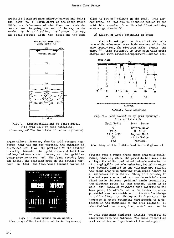
Vacuum Tube Design
trostatic lines are more sharply curved and bringthe beam to a focus short of the anode wherethere is a cross -over of electrons so that thebeam widens in going the rest of the way to theanode. As the grid voltage is lowered further,the focus recedes from the anode and the beam
MODEL OF TUBE 360MODEL SCALE 75:1
100 Ne 2
TRACES ON 360
70
50
30
20150
Nei
2
5
0 CATHODE
Ne / AT 0
Fig. 7 - Equipotential map on scale model,with grid No.1 at zero potential.
(Courtesy of The Institute of Radio Engineers)
trace widens. However, when the grid becomes neg-ative near the cut-off voltage, the emission isfirst cut off from the portions of the cathodedirectly beneath the grid wires and last fromhalfway between wires. Hence, as the grid be-comes more negative and the focus recedes fromthe anode, the emitting area on the cathode nar-rows so that the beam trace becomes narrow at
Fig. 8 - Beam traces on an anode.(Courtesy of The Institute of Radio Engineers)
close to cut-off voltage on the grid. This nar-row trace is not due to focusing action by thegrid but results from the restricted emittingarea at grid cut-off.
2) Effect of Anode Potential on Beams
When all voltages on the electrodes of atube with reference to cathode are varied in thesame proportion, the electron paths remain the
same. 10 This statement is true both with spacecharge and with cathode -temperature -limited con -
TUBE NI 360Nit
it
tt
I
t
i It
;
tI t
76 22.5 0 172
it
CATHODE
PARALLEL PLANE STRUCTURE
Fig. 9 - Beam formation by grid openings.No.2 volts = 250
No.1 Volts
0
22.522.5 -76
76172
Beam Focus
Before No.2On No.2
Beyond No.2At infinity
Virtual
(Courtesy of The Institute of Radio Engineers)
ditions over a range where space charge is negli-gible, that is, where the paths do not vary withvoltage for either unlimited cathode emission orwith negligible cathode emission, but if the emis-sion becomes limited as the voltages are raised,the paths change in changing from space charge toa limited -emission state. Thus, in a triode, ifthe voltages are varied so as to maintain somefixed ratio between grid and anode potentials,the electron paths do not change. Since it isonly the ratio of voltages that determines thebeam path, the effect of a variation in anodepotential can be considered in terms of a changein grid voltage in the opposite direction. An
increase of anode potential corresponds to a de-crease in the magnitude of the grid voltage. If
the grid voltage is negative, a decrease in its
10 This statement neglects initial velocity ofelectrons from the cathode. The small velocitiesthat exist become important at low voltages.
240
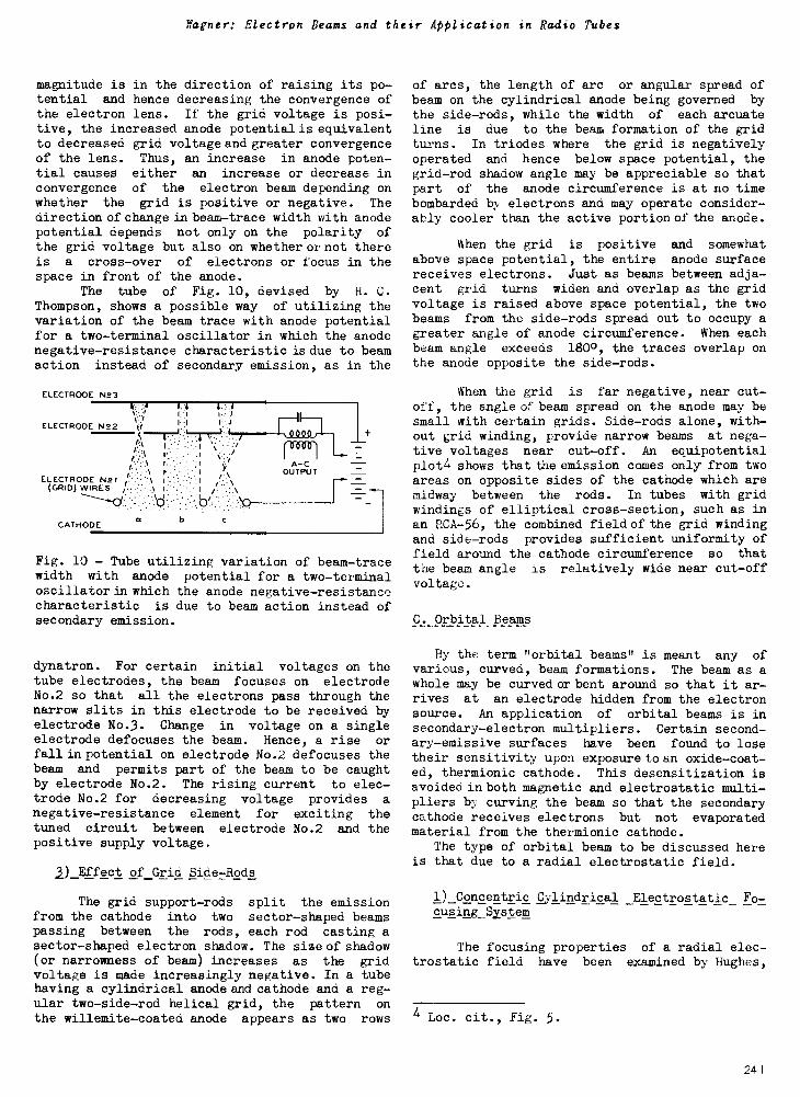
Wagner: Electron Beams and their Application in Radio Tubes
magnitude is in the direction of raising its po-tential and hence decreasing the convergence ofthe electron lens. If the grid voltage is posi-tive, the increased anode potential is equivalentto decreased grid voltage and greater convergenceof the lens. Thus, an increase in anode poten-tial causes either an increase or decrease inconvergence of the electron beam depending onwhether the grid is positive or negative. Thedirection of change in beam -trace width with anodepotential depends not only on the polarity ofthe grid voltage but also on whether or not thereis a cross -over of electrons or focus in thespace in front of the anode.
The tube of Fig. 10, devised by H. C.
Thompson, shows a possible way of utilizing thevariation of the beam trace with anode potentialfor a two -terminal oscillator in which the anodenegative -resistance characteristic is due to beamaction instead of secondary emission, as in the
ELECTRODE N53
ELECTRODE N52
ELECTRODE Ns I(GRID) WIRES
CATHODEa b C
Fig. 10 - Tube utilizing variation of beam -tracewidth with anode potential for a two -terminaloscillator in which the anode negative -resistancecharacteristic is due to beam action instead ofsecondary emission.
dynatron. For certain initial voltages on thetube electrodes, the beam focuses on electrodeNo.2 so that all the electrons pass through thenarrow slits in this electrode to be received byelectrode No.3. Change in voltage on a singleelectrode defocuses the beam. Hence, a rise orfall in potential on electrode No.2 defocuses thebeam and permits part of the beam to be caughtby electrode No.2. The rising current to elec-trode No.2 for decreasing voltage provides a
negative -resistance element for exciting thetuned circuit between electrode No.2 and thepositive supply voltage.
2) Effect of Grid Side -Rods
The grid support -rods split the emissionfrom the cathode into two sector -shaped beamspassing between the rods, each rod casting asector -shaped electron shadow. The size of shadow(or narrowness of beam) increases as the gridvoltage is made increasingly negative. In a tubehaving a cylindrical anode and cathode and a reg-ular two -side -rod helical grid, the pattern on
the willemite-coated anode appears as two rows
of arcs, the length of arc or angular spread ofbeam on the cylindrical anode being governed bythe side -rods, while the width of each arcuateline is due to the beam formation of the gridturns. In triodes where the grid is negativelyoperated and hence below space potential, thegrid -rod shadow angle may be appreciable so thatpart of the anode circumference is at no timebombarded by electrons and may operate consider-ably cooler than the active portion of the anode.
When the grid is positive and somewhatabove space potential, the entire anode surfacereceives electrons. Just as beams between adja-cent grid turns widen and overlap as the gridvoltage is raised above space potential, the twobeams from the side -rods spread out to occupy agreater angle of anode circumference. When eachbeam angle exceeds 1800, the traces overlap onthe anode opposite the side -rods.
When the grid is far negative, near cut-off, the angle of beam spread on the anode may besmall with certain grids. Side -rods alone, with-out grid winding, provide narrow beams at nega-tive voltages near cut-off. An equipotentialplot4 shows that the emission comes only from twoareas on opposite sides of the cathode which aremidway between the rods. In tubes with gridwindings of elliptical cross-section, such as inan RCA -56, the combined field of the grid windingand side -rods provides sufficient uniformity offield around the cathode circumference so that
the beam angle is relatively wide near cut-offvoltage.
C. Orbital Beams
By the term "orbital beams" is meant any ofvarious, curved, beam formations. The beam as awhole may be curved or bent around so that it ar-rives at an electrode hidden from the electronsource. An application of orbital beams is insecondary -electron multipliers. Certain second-ary -emissive surfaces have been found to losetheir sensitivity upon exposure to an oxide -coat-ed, thermionic cathode. This desensitization isavoided in both magnetic and electrostatic multi-pliers b:; curving the beam so that the secondarycathode receives electrons but not evaporatedmaterial from the thermionic cathode.
The type of orbital beam to be discussed hereis that due to a radial electrostatic field.
1) Concentric Cylindrical Electrostatic Fo-cusiRg_System
The focusing properties of a radial elec-trostatic field have been examined by Hughes,
4 Loc. cit., Fig. 5.
24 I
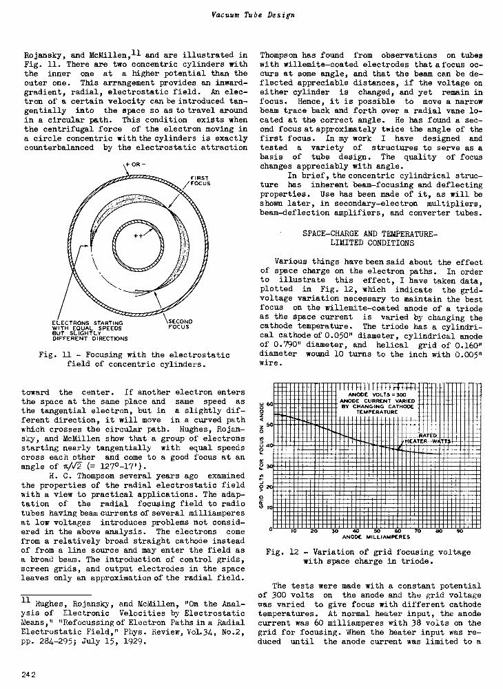
Vacuum Tube Design
Rojansky, and McMillen,11 and are illustrated inFig. 11. There are two concentric cylinders withthe inner one at a higher potential than theouter one. This arrangement provides an inward -gradient, radial, electrostatic field. An elec-tron of a certain velocity can be introduced tan-gentially into the space so as to travel aroundin a circular path. This condition exists whenthe centrifugal force of the electron moving ina circle concentric with the cylinders is exactlycounterbalanced by the electrostatic attraction
ELECTRONS STARTINGWITH EQUAL SPEEDSBUT SLIGHTLYDIFFERENT DIRECTIONS
FIRST/ FOCUS
\SECONDFOCUS
Fig. 11 - Focusing with the electrostaticfield of concentric cylinders.
toward the center. If another electron entersthe space at the same place and same speed as
the tangential electron, but in a slightly dif-ferent direction, it will move in a curved pathwhich crosses the circular path. Hughes, Rojan-sky, and McMillen show that a group of electronsstarting nearly tangentially with equal speedscross each other and come to a good focus at anangle of n/V (. 127°-17').
H. C. Thompson several years ago examinedthe properties of the radial electrostatic fieldwith a view to practical applications. The adap-tation of the radial focusing field to radiotubes having beam currents of several milliamperesat low voltages introduces problems not consid-ered in the above analysis. The electrons comefrom a relatively broad straight cathode insteadof from a line source and may enter the field asa broad beam. The introduction of control grids,screen grids, and output electrodes in the spaceleaves only an approximation of the radial field.
11 Hughes, Rojansky, and McMillen, "On the Anal-ysis of Electronic Velocities by ElectrostaticMeans," "Refocussing of Electron Paths in a RadialElectrostatic Field," Phys. Review, Vol.34, No.2,pp. 284-295; July 15, 1929.
Thompson has found from observations on tubeswith willemite-coated electrodes that afocus oc-curs at some angle, and that the beam can be de-flected appreciable distances, if the voltage oneither cylinder is changed, and yet remain infocus. Hence, it is possible to move a narrowbeam trace back and forth over a radial vane lo-cated at the correct angle. He has found a sec-ond focus at approximately twice the angle of thefirst focus. In my work I have designed and
tested a variety of structures to serve as abasis of tube design. The quality of focuschanges appreciably with angle.
In brief, the concentric cylindrical struc-ture has inherent beam -focusing and deflectingproperties. Use has been made of it, as will beshown later, in secondary -electron multipliers,beam -deflection amplifiers, and converter tubes.
SPACE -CHARGE AND TEMPERATURE-LIMITED CONDITIONS
Various things have been said about the effectof space charge on the electron paths. In orderto illustrate this effect, I have taken data,plotted in Fig. 12, which indicate the grid -voltage variation necessary to maintain the bestfocus on the willemite-coated anode of a triodeas the space current is varied by changing thecathode temperature. The triode has a cylindri-cal cathode of 0.050" diameter, cylindrical anodeof 0.790" diameter, and helical grid of 0.160"diameter wound 10 turns to the inch with 0.005"wire.
0m 600z
SO
00Du 400
rc030O
0 20
0cc
10
0
1 I I I I I IIIII41III1IANODE VOLTS = 300
ANODE CURRENT VARIEDBY CHANGING CATHODE
TEMPERATURE
RATEDTEFI W 5H E T T
10 20 30 40 50 60 70ANODE MILLIAMPERES
80 90
Fig. 12 - Variation of grid focusing voltagewith space charge in triode.
The tests were made with a constant potentialof 300 volts on the anode and the grid voltagewas varied to give focus with different cathodetemperatures. At normal heater input, the anodecurrent was 60 milliamperes with 38 volts on thegrid for focusing. When the heater input was re-duced until the anode current was limited to a
242
Wagner: Electron Beams and their Application in Radio Tubes
small fraction of the space -charge current (ob-servations made for anode currents as low as 0.1milliampere), the potential on the grid had tobe raised to 55 volts for best focus.
The need for raising the grid voltage to re-store focus when the cathode temperature andspace current were reduced can be considered interms of the changing convergence of the gridlens. Reduction of space current causes a risein potential throughout the space between theelectrodes. The grid voltage, if unchanged, thenbecomes relatively lower with respect to thespace and hence the lens formed by the grid wiresbecomes more convergent, and brings the electrons,which were in focus on the anode, to a focus shortof the anode. The grid voltage must be raisedto refocus on the anode and show the minimum beam -trace width.
SOME APPLICATIONS OF BEAMS INCOMMERCIAL TUBES
The following table gives instances of theutilization of beams in commercial tubes.
Application Tube Type Date
A. Reversed grid windings 47 1929B. Elliptical grid 56, 57,58 1931C. Magic eye 6E5 1935D. Beam power tube 6L6 1936E. Low -noise, low -screen- EF-9
current tube (Philips) 1937F. Anodes of small
dimensions 6K8, 1851 1938
A. Reversed Grid Windings
In the early development of power output tubesusing screen grids, it was noticed that some ofthe screen -grid wires in sample tubes operatedred hot while others were cool. This effect, ex-plained by W. R. Ferris in U.S. Patent 2,047,019was due to the impinging of electron beams formedbetween the control -grid wires which happened tohe positioned approximately halfway between thecontrol -grid turns. At that time the controlgrid and screen grid were wound in the same di-rection, so that complete screen -grid turns couldbe exposed to the electron beams from the controlgrid. This arrangement was changed in the abovepatent by winding one of the grids right-handedand the other left-handed so as to permit bom-bardment of only portions of the screen -gridturns, instead of complete turns. In this way,the maximum screen -grid temperature was loweredbecause of heat conduction from the short bom-barded lengths or arcs of the screen -grid wire.
Tubes using reversed grid windings have beenreferred to as anti -beam tubes because of thechopping up of the control -grid beams by thescreen grid. However, the Ferris patent shows
diagrammatically the presence of the beams andcovers an invention based upon their knowledge.
B. Elliptical Grid
One effect of a grid side -rod, as has alreadybeen mentioned, is to leave a gap in the spacecurrent to the anode. There is also an increasein amplification factor around the cathode cir-cumference in the neighborhood of the side -rodsof such a magnitude that with a circular cross-section grid the region on the cathode beneaththe side -rods may be practically non -emittingthroughout most of the negative grid -voltagerange. In order to get a more uniform cut-offand an increased active emitting arc of cathode(B.Salzberg, U.S. Patents 2,073,946and 2,100,723)the spacing is increased between grid side -rodsto make an almost elliptical grid. The sector -shaped beams due to the wide -spaced side -rods ofthe elliptical grid are relatively wide even athigh grid bias.
C. Magic Eye
The magic eye (H. M. Wagner, U.S. Patents2,051,189 and 2,122,268) uses a vane or narrowstrip parallel to a cylindrical cathode for con-trolling the angular portion of illuminated areaon a conical target. The action is similar tothat of a grid side -rod in shadowing a certainarc of anode circumference from the space current.The vane splits the beam of electrons and leavessharp -edged traces on the target; the more neg-ative (less positive) the vane, the wider thebeam is split, and the larger the sector of darkarea on the target. A short helix surrounds andis welded to the cathode of the eye. Its func-tion is to limit the target current. The wireof the helix causes some disturbance in the elec-trostatic field and introduces in the beam vel-ocity components of varying amounts parallel tothe vane. The presence of the helix results insome loss of beam sharpness, but the loss is tooslight to notice without close examination. Thehelix, which is at cathode potential, gives adiffused spiral pattern on the target. The spi-ral -beam trace is broad enough so that adjacentturns overlap and merge to approximate the ap-pearance of uniform illumination.
D. Beam Power Tube
The beam power tube,8 in contrast to otherpower tubes having reversed control -grid andscreen -grid windings, uses grids of equal pitchwound in the same sense and assembled so that theturns on the two grids are in alignment. Thebeams formed by the control -grid wires pass al-most entirely between the screen -grid turns. Thescreen current is materially reduced and hence
a Loc. cit.
243
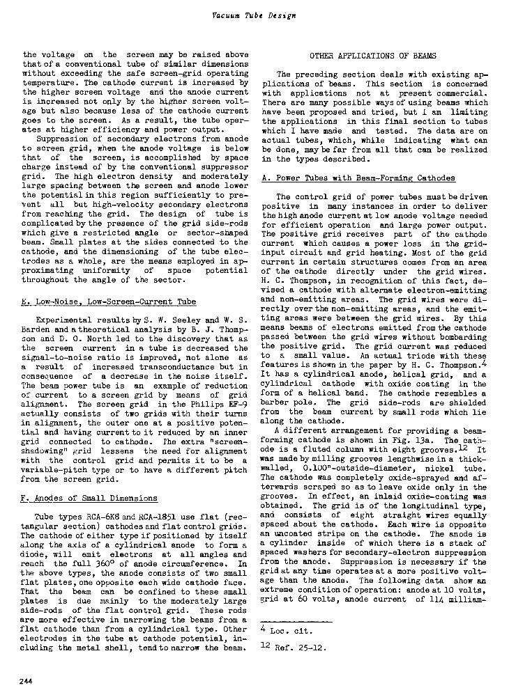
Vacuum Tube Design
the voltage on the screen may be raised abovethat of a conventional tube of similar dimensionswithout exceeding the safe screen -grid operatingtemperature. The cathode current is increased bythe higher screen voltage and the anode currentis increased not only by the higher screen volt-age but also because less of the cathode currentgoes to the screen. As a result, the tube oper-ates at higher efficiency and power output.
Suppression of secondary electrons from anodeto screen grid, when the anode voltage is belowthat of the screen, is accomplished by spacecharge instead of by the conventional suppressorgrid. The high electron density and moderatelylarge spacing between the screen and anode lowerthe potential in this region sufficiently to pre-vent all but high -velocity secondary electronsfrom reaching the grid. The design of tube iscomplicated by the presence of the grid side -rodswhich give a restricted angle or sector -shapedbeam. Small plates at the sides connected to thecathode, and the dimensioning of the tube elec-trodes as a whole, are the means employed in ap-proximating uniformity of space potentialthroughout the angle of the sector.
E. Low -Noise, Low -Screen -Current Tube
Experimental results by S. W. Seeley and W. S.Barden and atheoretical analysis by B. J. Thomp-son and D. O. North led to the discovery that asthe screen current in a tube is decreased thesignal-to-noise ratio is improved, not alone asa result of increased transconductance but inconsequence of a decrease in the noise itself.The beam power tube is an example of reductionof current to a screen grid by means of gridalignment. The screen grid in the Philips EF-9actually consists of two grids with their turnsin alignment, the outer one at a positive poten-tial and having current to it reduced by an innergrid connected to cathode. The extra "screen -shadowing" grid lessens the need for alignmentwith the control grid and permits it to be a
variable -pitch type or to have a different pitchfrom the screen grid.
F. Anodes of Small Dimensions
Tube types RCA -6K8 and RCA -1851 use flat (rec-tangular section) cathodes and flat control grids.The cathode of either type if positioned by itselfalong the axis of a cylindrical anode to form adiode, will emit electrons at all angles andreach the full 3600 of anode circumference. In
the above types, the anode consists of two smallflat plates, one opposite each wide cathode face.That the beam can be confined to these smallplates is due mainly to the moderately largeside -rods of the flat control grid. These rodsare more effective in narrowing the beams from aflat cathode than from a cylindrical type. Otherelectrodes in the tube at cathode potential, in-cluding the metal shell, tend to narrow the beam.
OTHER APPLICATIONS OF BEAMS
The preceding section deals with existing ap-plications of beams. This section is concernedwith applications not at present commercial.There are many possible ways of using beams whichhave been proposed and tried, but I am limitingthe applications in this final section to tubeswhich I have made and tested. The data are onactual tubes, which, while indicating what canbe done, maybe far from all that can be realizedin the types described.
A. Power Tubes with Beam -Forming Cathodes
The control grid of power tubes mustbedrivenpositive in many instances in order to deliverthe high anode current at low anode voltage neededfor efficient operation and large power output.The positive grid receives part of the cathodecurrent which causes a power loss in the grid -input circuit and grid heating. Most of the gridcurrent in certain structures comes from an areaof the cathode directly under the grid wires.H. C. Thompson, in recognition of this fact, de-vised a cathode with alternate electron -emittingand non -emitting areas. The grid wires were di-rectly over the non -emitting areas, and the emit-ting areas were between the grid wires. By thismeans beams of electrons emitted from the cathodepassed between the grid wires without bombardingthe positive grid. The grid current was reducedto a small value. An actual triode with thesefeatures is shown in the paper by H. C. Thompson.4It has a cylindrical anode, helical grid, and acylindrical cathode with oxide coating in theform of a helical band. The cathode resembles abarber pole. The grid side -rods are shieldedfrom the beam current by small rods which liealong the cathode.
A different arrangement for providing a beam -forming cathode is shown in Fig. 13a. The cath-ode is a fluted column with eight grooves.12 Itwas made by milling grooves lengthwise in a thick-walled, 0.100" -outside -diameter, nickel tube.The cathode was completely oxide -sprayed and af-terwards scraped so as to leave oxide only in thegrooves. In effect, an inlaid oxide -coating wasobtained. The grid is of the longitudinal type,and consists of eight straight wires equallyspaced about the cathode. Each wire is oppositean uncoated stripe on the cathode. The anode isa cylinder inside of which there is a stack ofspaced washers for secondary -electron suppressionfrom the anode. Suppression is necessary if thegrid at any time operates at a more positive volt-age than the anode. The following data show anextreme condition of operation: anode at 10 volts,grid at 60 volts, anode current of 114 milliam-
4 Loc. cit.
12 Ref. 25-12.
244
Wagner: Electron Beams and their Application in Radio Tubes
CROSS-SECTIONAL VIEWLOOKING AT END OF TUBE
BARENICKEL
O
COAT INGDEOXI
N ICKELCATHODE SLEEVE
0
GRIDWIRE
SECONDARY -ELECTRON 0?SUPPRESSINGANODE
.:.**CROSS-SECTIONALVIEW LOOKING ATSIDE OF ANODEASSEMBLY
(SEE FIG. 13 b)
ELECTRON BEAMFOR GRID POTENTIALMORE POSITIVE THANSPACE POTENTIAL
Fig. 13a - "Currentless grid" beam triode withcolumnar cathode having oxide -coated flutes.
peres, and grid current of 9 milliamperes. Thegrid receives only 8 per cent of the anode cur-rent when its voltage is six times as positiveas the anode. When the grid and anode are bothat 60 volts, their currents are 3.1 and 181 milli-amperes, respectively. It will be noted thatthe grid current is less than 2 per cent of theanode current.1.3
Although the data just presented are for a
tube of small power, it is of interest to considerthe ultimate size of tube of this general typethat may be built. The oxide -coated cathode hasreceived a bad reputation for use in power tubesof large size and at high voltages. This reputa-tion is to a large extent due to unsuccessfulattempts to design large tubes without the appli-cation of beam principles. I am convinced thatby proper use of beams it will be possible toextend the voltage and power rating of tubeswith oxide -coated cathodes far in excess of pres-ent limits. The cathode-ray tube is an exampleof the successful application of the oxide -coatedcathode at high voltage and high electron -emissiondensity and offers encouragement in the power -tube field. Grid emission due to grid'heating isone of the important limitations in power -tubedesign. The absence of grid heating by electronbombardment in beam tubes, is an important stepin avoiding grid emission.
13Ref. 25-13.
Fig. 13b shows a photograph of the cathode -grid assembly and a photograph of the anode as-sembly for a triode of moderately large size de-signed by me three years ago. The cathode has adiameter of 0.800" and 30 oxide -coated stripes2-1/4" long. This tube, tested with 150 volts
Fig. 13b - Top: Grid -cathode assemblyof large beam power tube with oxide -
coated flutes in cathode sleeve.Bottom: Anode assembly of same tube.
245
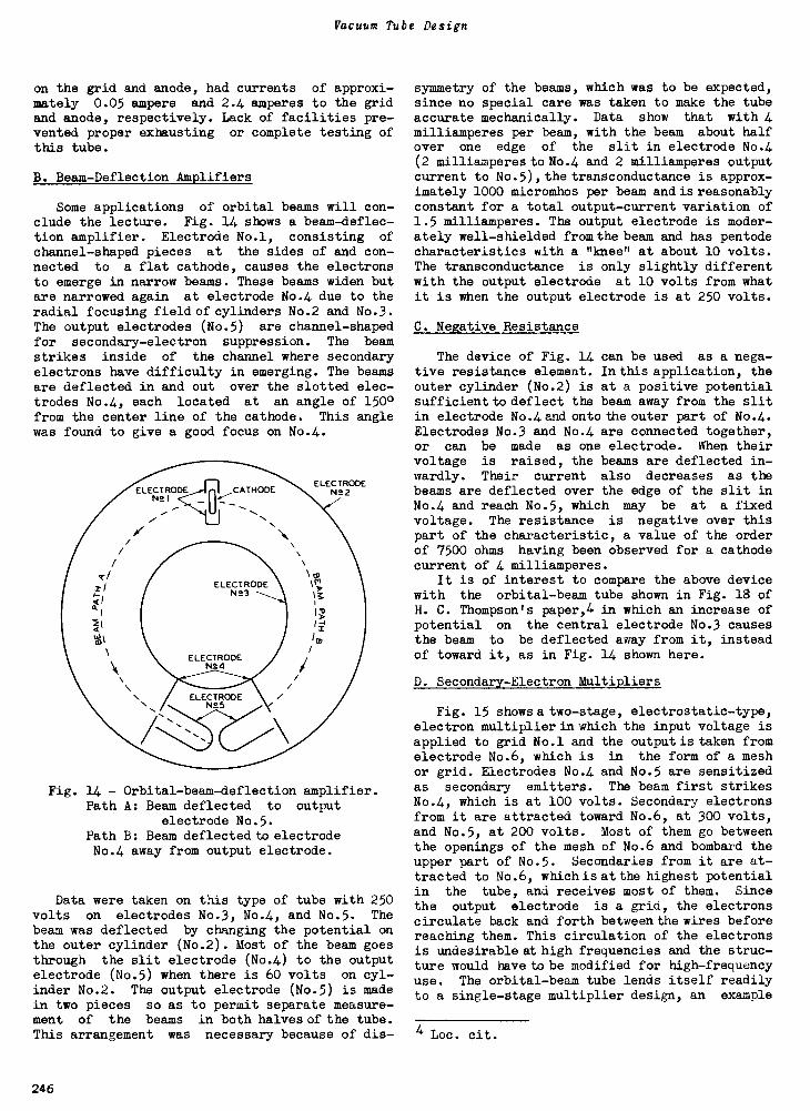
Vacuum Tube Design
on the grid and anode, had currents of approxi-mately 0.05 ampere and 2.4 amperes to the gridand anode, respectively. Lack of facilities pre-vented proper exhausting or complete testing ofthis tube.
B. Beam -Deflection Amplifiers
Some applications of orbital beams will con-clude the lecture. Fig. 14 shows a beam -deflec-tion amplifier. Electrode No.1, consisting of
channel -shaped pieces at the sides of and con-nected to a flat cathode, causes the electronsto emerge in narrow beams. These beams widen butare narrowed again at electrode No.4 due to theradial focusing field of cylinders No.2 and No.3.The output electrodes (No.5) are channel -shapedfor secondary -electron suppression. The beamstrikes inside of the channel where secondaryelectrons have difficulty in emerging. The beamsare deflected in and out over the slotted elec-trodes No.4, each located at an angle of 1500from the center line of the cathode. This anglewas found to give a good focus on No.4.
ELECTRODEN2 I
A(
CATHODEELECTRODE
N'22
Fig. 14 - Orbital -beam -deflection amplifier.Path A: Beam deflected to output
electrode No.5.Path B: Beam deflected to electrodeNo.4 away from output electrode.
Data were taken on this type of tube with 250volts on electrodes No.3, No.4, and No.5. Thebeam was deflected by changing the potential onthe outer cylinder (No.2). Most of the beam goesthrough the slit electrode (No.4) to the outputelectrode (No.5) when there is 60 volts on cyl-inder No.2. The output electrode (No.5) is madein two pieces so as to permit separate measure-ment of the beams in both halves of the tube.This arrangement was necessary because of dis-
symmetry of the beams, which was to be expected,since no special care was taken to make the tubeaccurate mechanically. Data show that with 4milliamperes per beam, with the beam about halfover one edge of the slit in electrode No.4(2 milliamperes to No.4 and 2 milliamperes outputcurrent to No.5),the transconductance is approx-imately 1000 micromhos per beam and is reasonablyconstant for a total output -current variation of1.5 milliamperes. The output electrode is moder-ately well -shielded from the beam and has pentodecharacteristics with a "knee" at about 10 volts.The transconductance is only slightly differentwith the output electrode at 10 volts from whatit is when the output electrode is at 250 volts.
C. Negative Resistance
The device of Fig. 14 can be used as a nega-tive resistance element. In this application, theouter cylinder (No.2) is at a positive potentialsufficient to deflect the beam away from the slitin electrode No.4 and onto the outer part of No.4.Electrodes No.3 and No.4 are connected together,or can be made as one electrode. When theirvoltage is raised, the beams are deflected in-wardly. Their current also decreases as thebeams are deflected over the edge of the slit inNo.4 and reach No.5, which may be at a fixedvoltage. The resistance is negative over thispart of the characteristic, a value of the orderof 7500 ohms having been observed for a cathodecurrent of 4 milliamperes.
It is of interest to compare the above devicewith the orbital -beam tube shown in Fig. 18 ofH. C. Thompson's paper,4 in which an increase ofpotential on the central electrode No.3 causesthe beam to be deflected away from it, insteadof toward it, as in Fig. 14 shown here.
D. Secondary -Electron Multipliers
Fig. 15 shows a two -stage, electrostatic -type,electron multiplier in which the input voltage isapplied to grid No.1 and the output is taken fromelectrode No.6, which is in the form of a meshor grid. Electrodes No.4 and No.5 are sensitizedas secondary emitters. The beam first strikesNo.4, which is at 100 volts. Secondary electronsfrom it are attracted toward No.6, at 300 volts,and No.5, at 200 volts. Most of them go betweenthe openings of the mesh of No.6 and bombard theupper part of No.5. Secondaries from it are at-tracted to No.6, whichisatthe highest potentialin the tube, and receives most of them. Sincethe output electrode is a grid, the electronscirculate back and forth between the wires beforereaching them. This circulation of the electronsis undesirable at high frequencies and the struc-ture would have to be modified for high -frequencyuse. The orbital -beam tube lends itself readilyto a single -stage multiplier design, an example
4 Loc. cit.
246
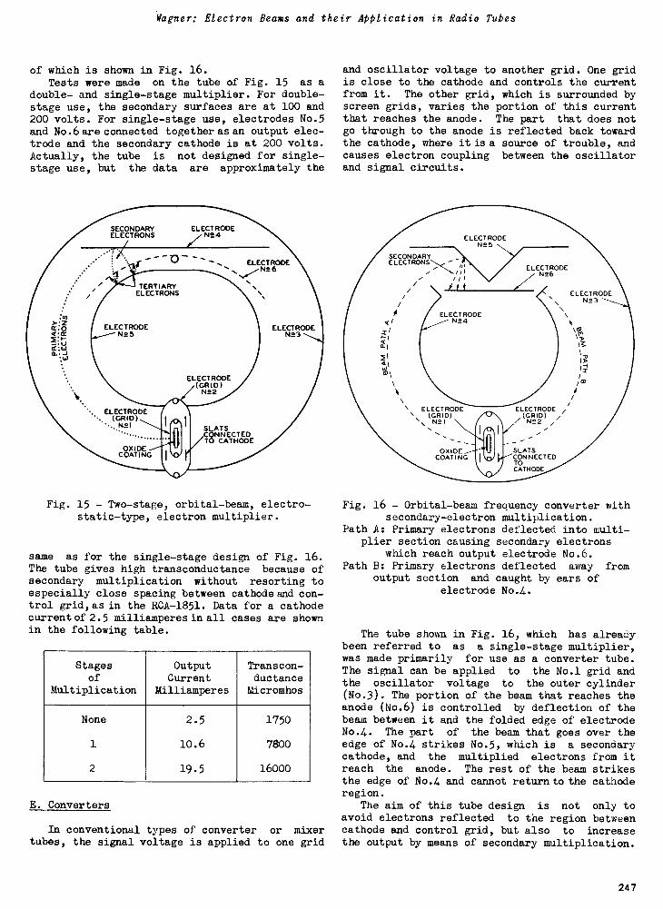
Wagner: Electron Beams and their Application in Radio Tubes
of which is shown in Fig. 16.Tests were made on the tube of Fig. 15 as a
double- and single -stage multiplier. For double -stage use, the secondary surfaces are at 100 and200 volts. For single -stage use, electrodes No.5and No.6areconnected together as an output elec-trode and the secondary cathode is at 200 volts.Actually, the tube is not designed for single -stage use, but the data are approximately the
SECONDARY ELECTRODEELECTRONS N24
(o))- Zor 0a¢ N2 52 PG
a.
TERTIARYELECTRONS
ELECTRODE
ELECTRODE. (GRID ) ...NSA
...........
OXIDECOATING
ELECTRODE(GRID)
NS2
ELECTRODEN26
SLATSCONNECTED
/TO CATHODE
ELECTRODEN23
Fig. 15 - Two -stage, orbital -beam, electro-static -type, electron multiplier.
same as for the single -stage design of Fig. 16.The tube gives high transconductance because ofsecondary multiplication without resorting toespecially close spacing between cathode and con-trol grid,as in the RCA -1851. Data for a cathodecurrent of 2.5 milliamperes in all cases are shownin the following table.
Stagesof
Multiplication
OutputCurrent
Milliamperes
Transcon-ductanceMicromhos
None
1
2
2.5
10.6
19.5
1750
7800
16000
E. Converters
In conventional types of converter or mixertubes, the signal voltage is applied to one grid
and oscillator voltage to another grid. One gridis close to the cathode and controls the currentfrom it. The other grid, which is surrounded byscreen grids, varies the portion of this currentthat reaches the anode. The part that does notgo through to the anode is reflected back towardthe cathode, where it is a source of trouble, andcauses electron coupling between the oscillatorand signal circuits.
ELECTRODEN!5
SECONDARYELECTRONS',
III
ELECTRODEQ/ NE4
211-1
m\
\ ELECT RODE\ (GRID)N2. I
OXIDECOATING
Fig. 16 - Orbital -beam frsecondary -electron
Path A: Primary electronsplier section causing
which reach outputPath B: Primary electrons
output section andelectrode
ELECTRODENE.6
ELECTRODEN.23
im
ELECTRODE
N52 ,
SLATSCONNECTEDTOCATHODE
equency converter withmultiplication.deflected into multi -
secondary electronselectrode No.6.deflected away from
caught by ears ofNo.4.
The tube shown in Fig. 16, which has alreadybeen referred to as a single -stage multiplier,was made primarily for use as a converter tube.The signal can be applied to the No.1 grid andthe oscillator voltage to the outer cylinder(No.3). The portion of the beam that reaches theanode (No.6) is controlled by deflection of thebeam between it and the folded edge of electrodeNo.4. The part of the beam that goes over theedge of No.4 strikes No.5, which is a secondarycathode, and the multiplied electrons from itreach the anode. The rest of the beam strikesthe edge of No.4 and cannot return to the cathoderegion.
The aim of this tube design is not only toavoid electrons reflected to the region betweencathode and control grid, but also to increasethe output by means of secondary multiplication.
247

Vacuum Tube Design
The secondary cathode (No.5) has a secondary - Output -Electrode Current 3.5 milliamperesemission ratio of 3.3 at 150 volts. The dataare approximately as follows:
Total Cathode CurrentPeak Oscillator Voltage
3.5 milliamperes
(applied to beam - 20 volts
Conversion Conductance 1500 micromhos deflection electrode)Maximum Voltage Average Current
on any electrode 250 volts to beam -deflection <10 microamperes
Output -Electrode Voltage 250 volts electrode
248
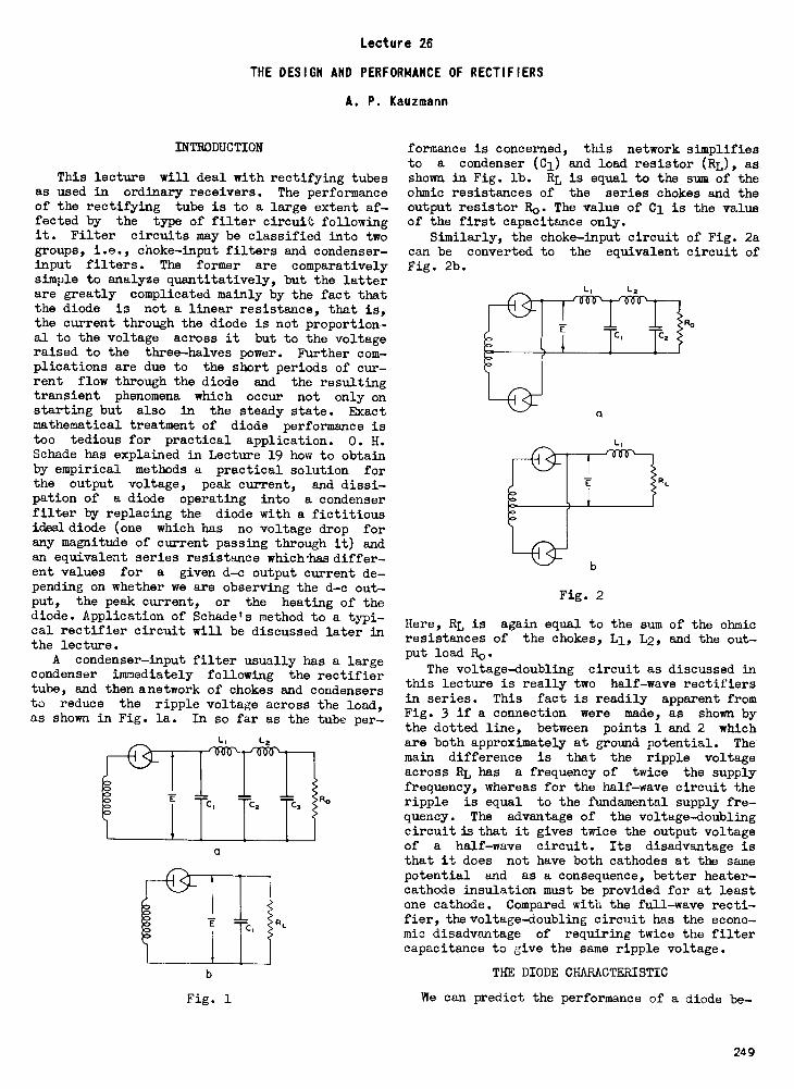
Lecture 26
THE DESIGN AND PERFORMANCE OF RECTIFIERS
A. P. Kauzmann
INTRODUCTION
This lecture will deal with rectifying tubesas used in ordinary receivers. The performanceof the rectifying tube is to a large extent af-fected by the type of filter circuit followingit. Filter circuits may be classified into twogroups, i.e., choke -input filters and condenser -input filters. The former are comparativelysimple to analyze quantitatively, but the latterare greatly complicated mainly by the fact thatthe diode is not a linear resistance, that is,the current through the diode is not proportion-al to the voltage across it but to the voltageraised to the three -halves power. Further com-plications are due to the short periods of cur-rent flow through the diode and the resultingtransient phenomena which occur not only onstarting but also in the steady state. Exactmathematical treatment of diode performance istoo tedious for practical application. 0. H.Schade has explained in Lecture 19 how to obtainby empirical methods a practical solution forthe output voltage, peak current, and dissi-pation of a diode operating into a condenserfilter by replacing the diode with a fictitiousideal diode (one which has no voltage drop forany magnitude of current passing through it) andan equivalent series resistance whichhas differ-ent values for a given d -c output current de-pending on whether we are observing the d -c out-put, the peak current, or the heating of thediode. Application of Schadets method to a typi-cal rectifier circuit will be discussed later inthe lecture.
A condenser -input filter usually has a largecondenser immediately following the rectifiertube, and then anetwork of chokes and condensersto reduce the ripple voltage across the load,as shown in Fig. la. In so far as the tube per -
a
b
Fig. 1
formance is concerned, this network simplifiesto a condenser (C1) and load resistor (RL), asshown in Fig. lb. RL is equal to the sum of theohmic resistances of the series chokes and theoutput resistor Ro. The value of Cl is the valueof the first capacitance only.
Similarly, the choke -input circuit of Fig. 2acan be converted to the equivalent circuit ofFig. 2b.
a
Fig. 2
Here, RL is again equal to the sum of the ohmicresistances of the chokes, Li, L2, and the out-put load Ro.
The voltage -doubling circuit as discussed inthis lecture is really two half -wave rectifiersin series. This fact is readily apparent fromFig. 3 if a connection were made, as shown bythe dotted line, between points 1 and 2 whichare both approximately at ground potential. Themain difference is that the ripple voltageacross RL has a frequency of twice the supplyfrequency, whereas for the half -wave circuit theripple is equal to the fundamental supply fre-quency. The advantage of the voltage -doublingcircuit is that it gives twice the output voltageof a half -wave circuit. Its disadvantage isthat it does not have both cathodes at the samepotential and as a consequence, better heater -cathode insulation must be provided for at leastone cathode. Compared with the full -wave recti-fier, the voltage -doubling circuit has the econo-mic disadvantage of requiring twice the filtercapacitance to give the same ripple voltage.
THE DIODE CHARACTERISTIC
We can predict the performance of a diode be -
249
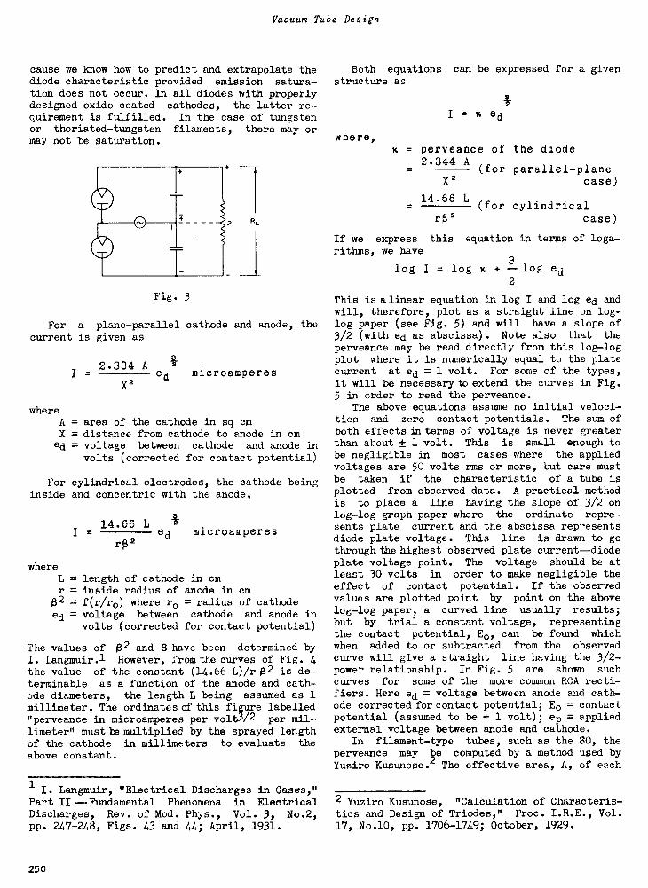
Vacuum Tube Design
cause we know how to predict and extrapolate thediode characteristic provided emission satura-tion does not occur. In all diodes with properlydesigned oxide -coated cathodes, the latter re-quirement is fulfilled. In the case of tungstenor thoriated-tungsten filaments, there may ormay not be saturation.
Fig. 3
For a plane -parallel cathode and anode, thecurrent is given as
I =2.334 A
ed2X2
microamperes
whereA = area of the cathode in sq cmX = distance from cathode to anode in cmed = voltage between cathode and anode in
volts (corrected for contact potential)
For cylindrical electrodes, the cathode beinginside and concentric with the anode,
I =14.66 L edI
microamperesrp2
whereL = length of cathode in cmr = inside radius of anode in cm
132 = f(r/r0) where 1.0 = radius of cathodeed = voltage between cathode and anode in
volts (corrected for contact potential)
The values of 02 and 0 have been determined byI. Langmuir.l However, from the curves of Fig. 4the value of the constant (14.66 L)/r 02 is de-terminable as a function of the anode and cath-ode diameters, the length L being assumed as 1millimeter. The ordinates of this fire labelled"perveance in microamperes per volt}/2 per mil-limeter" must be multiplied by the sprayed lengthof the cathode in millimeters to evaluate the
above constant.
1I. Langmuir, "Electrical Discharges in Gases,"
Part II - Fundamental Phenomena in ElectricalDischarges, Rev. of Mod. Phys., Vol. 3, No.2,pp. 247-248, Figs. 43 and 44; April, 1931.
Both equations can be expressed for a givenstructure as
a
I = x ed
where,w = perveance of the diode
2.344 A(for parallel -plane
X2 case)
14.66 L(for cylindrical
case)
If we express this equation in terms of loga-rithms, we have
log I = log x + -3 log ed2
This is a linear equation in log I and log ed andwill, therefore, plot as a straight line on log -log paper (see Fig. 5) and will have a slope of3/2 (with ed as abscissa). Note also that the
perveance may be read directly from this log -logplot where it is numerically equal to the platecurrent at ed = 1 volt. For some of the types,it will be necessary to extend the curves in Fig.5 in order to read the perveance.
The above equations assume no initial veloci-ties and zero contact potentials. The sum ofboth effects in terms of voltage is never greaterthan about ± 1 volt. This is small enough tobe negligible in most cases where the appliedvoltages are 50 volts rms or more, but care mustbe taken if the characteristic of a tube isplotted from observed data. A practical methodis to place a line having the slope of 3/2 onlog -log graph paper where the ordinate repre-sents plate current and the abscissa representsdiode plate voltage. This line is drawn to gothrough the highest observed plate current-diodeplate voltage point. The voltage should be atleast 30 volts in order to make negligible theeffect of contact potential. If the observedvalues are plotted point by point on the abovelog -log paper, a curved line usually results;
but by trial a constant voltage, representingthe contact potential, E0, can be found whichwhen added to or subtracted from the observedcurve will give a straight line having the 3/2 -power relationship. In Fig. 5 are shown suchcurves for some of the more common RCA recti-fiers. Here ed = voltage between anode and cath-ode corrected for contact potential; E0 = contactpotential (assumed to be + 1 volt); ep = appliedexternal voltage between anode and cathode.
In filament -type tubes, such as the 80, theperveance may pe computed by a method used byYuziro Kusunose. The effective area, A, of each
2 Yuziro Kusunose, "Calculation of Characteris-tics and Design of Triodes," Proc. I.R.E., Vol.17, No.10, pp. 1706-1749; October, 1929.
250
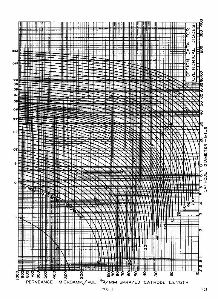
6IIP ANMS
... ...................ESSEEMBEI9 1M.ME=MME MEM= : i Ma FEL=.11:
.. MISM11110111111101 ..MIMI 111 IIIIMS U.... ha11111endese 1 MOM! Hi =MINN 11=M11111111 .....ME= MOM/1MM= HES 1
.. 2222112==121111.11..
.. --e"'fird
a..= ,.
2-22=1IliIIIIIM=
ocesmon.... . .: .MIMIIMM
Inr1:11111110AI
l ...=IIIINIMIIIIII . a
M
Iin Milinhi11.1.1.111111n Mill graligliarainIEWArirridhopliiimmu imeni
MMIMMIIMIIMMI I I III II MIMI .... 1111I111111 .1.---gramagramomur qui ii., lllllllll gIIIMIMil OM iiiiiiiiiiiiiiiiiiii iiiiiiiiii iinninininOMMEMEMMMMEMEMON Hifi inn Uni IMMO niiiiiiiiiiiiiiMUUMMEMEEMMUMM
111111111111114MIIIM11111111111111111111111111111111111111MEMEIMIMMIN11111111111111111111111111111111111111111 IIIIIIIIIIIIII 1111111111 MIIIIIMIIIIII IIIIIIIMMMI171 C HIJI111111111111111111111111111111111111 IIMIIIIIIIMIIMIIIIIIIIIIMIIIMMMIMIIIIIIIIIIMIMIIIIIIIIIIIIIIIIIIISIIIM IIIIIIIIIIMI llll IIIIIIIMMEMIIIIIIMMMIIN=minium mumuntunumminn um immummuumn niumums nom' .
MinniiMMIIIIIIIl ll
llll mum eraimmo sminniumommm mown= nomiiii imumiiiiiinumiliimmummimi allll 1111111 ll iiiir"! MUM iia"r......11.11.1M Ifill NUMMI 11111 i111111111111111M111111111111111111111111 IIMIIMI
-moons =m11011111111111 111111111111thififififilimmulUIMMINIIII1 i-
11111111
mui1:14211:1111::::i-" IIIIIiiiiM1 I
MIIMI111111111 lllll
29-1-11111.14-"Ahaammiiiiig:21111111111:911111.
- IIIIIIIIIIIIIIIIIIM1111111111.1a
wiliiiiimmulunniiii
ill
UMIII11111111111111;"lllll Imiumul111111ilmin:!!!"111111armni-......z.lfitipliii 111:1111 11111110111111311101111111 allll ll 11_1111ili 11111110E2.111111111.111111me-M1/111
inMilliiiin11111111 num
I:
:km lllll ° l ---...====--. llll .:- .:::74:Millai...
m ....... -:gl`...
ea
ll MIM.M1111..- -...1111111EDEMEIMM
ll as. lll .,,MMO ll..
..... ......
.... ....... . .. ............
..... .. ... . .. .... 111 .. . 2 . !me
... .11111 . I .... . ...1! ... 11:1776. .4:1M 441 . . --.1"
lllll....... - . 11=1.111.. - . MM.,..,...,.....,M
EOM .., "...IMikMus.- MEM.- MM. 1.- MEM- MOI ,Il -...7 -.Mh..,.--" '`
..... .."."
. -- I
.... ".
.
.. :RI. I . ! .. . B. -..
.. .. :.
14 Zin
.111111
.7. ...... ---...nias.:_..4 111111.8...41Mi72 MINEZT 111M.I. Illp..1.;:..... .. .. ..-....1.1110.1711.11...1111.:"..a.:.........41
..z 7.1IN .._111111.. -.0111.7"...11111......al..-',E11.."411
. 11.:Z.IM111.1.7.11111....1111.7.....1111.....MI16.!.1
....IN no.,.......,..,... a.
i ii!iiiii ........
9 ... ;....
ems . i . . .... ..
..
0....... ,11111111110 I \ NOWIIIIM101111111 11611 VIM
' S"'".:.:"..7,:liZEMNEZMUM. .. illi.,sX.,LIOEtZTAkiniTA
,: 'grAZGLET:M=MM
NOVNAMLIIIIIIIIMMINVIIIIIi111111111
... Iiiii lin.. !I! NEMIINZ.. 4111111101/ MI 0.111041.11Z .111114 ., IMI \ MS MOMIMMILIMINELINI.
MI In . din .1.111..- RIM lie ...Ma 11.1...111117:5111!.11! . 1.4 4 111111.111111.11O11111.1k11141111111.111111111111M111111..ii.._ 111111 in........1.111111111...... Ill ....111111414..51114.0.111MI...."..41.1.7...411..91. .. IIi.. I II 111:111110111114 7O .. . 11111110WL1111111111111.1111111M.11117. ..... IIIMINuir'LMIIIIIIIR ... .;"111111114.71.11111111111iZNINIIIN.Illnii:5110.11111b4111.. I 6;111 II 'II111010111110111p17 , ma mkOIMILIIIIIMMIIIII&U1111111.n.i.:.!111011191B.M.:rillfiligimi:211110.1i=911111WVIMIliaTIIIIii."Millaal111.1:1111i:1111i5111 4.:14:(0.mounziaslosmsomwmailwmalummaipun. ,...19=muiniz...loilmna...iimazmumomininikimeinei:911i2:1 .111 111:1111.:1106:110111111.1\ 4MIIMAIINLMUMMIIIIIIIIKIDiNiam=i4:rnamolifiltliiniNvolimpii;riiimniivimi.rimaimoir.m:Pithogikookookon ..11.:1011011:11-11111:11IIMILIIIiweamninuaminn "!fisfinivii mai Twulupar Niummi-meillueliami...mnouhrguasioiin milmi:11010101:10111g1IIIIVIOILIIVIIIVELIIILINIPlfiliiii11111=i;212 111111114111=4224iiniii20111111:29ON611M3 \ OM Ilii:!Ilii2:111:11i111i wfit;!fingfi:1:11%11111111111A11111101111111111"NIIIIiiir "41111111 IMIliii.'"911111111.13:91111111:25411111101111120MON101111in110111211; Ili:11010.A91:1:1i10711111 \ II1W11.1111111111111111!!!!!IfilisigH1.1111ii ...291111111111iiia91111111i:5111110.111110.41111aIliT11162!111011i2111;! 011;91;91.11:101!VIN1111M11110111V111111111111111; tilMisiZMIlli iiiM2Pliiii.29111111ii:SIIIii21111i2111111040111ii:911i011i1,1011;:9101i:1001:1i11!iIN111111111111111A111111111
innitliPliilliiiiiglillifliiiiiii:Iiiiii:Ilikiiiiligililigli121!1:11;bililti . .1111;111RIRILiiiiiiii.ISPIlliiiigit11!11111rlkaLgValiltIll, .
.... -.. :!Pii!Pi;tfmag-N.Ezplogniri,-,.... "" .. -L--..mr.:..1==_ __......_._
'41filimhu, milmzuli iillkirT".=5.T...mom.raill....i....... . Is sililislalz r- IE =THU inn ... 4111111::'l:sEn . ""- "'"'L.71WA:',NPALTE=EZ=111011111:7" ... .2 a =.4... ..... --IMM,M11111010 .. ....
C ill CI Ill% . ........ -2-1.zz.moazezmw 9" :2 2.9:: . 1 .. - WM ME GM ,.....1 a..
I 1. Nail...Z van....m.......mmr.. '1=i1,1: 2 ....imili
iiisa.. 7. ki... ELT UM -4111111..,1=.., I='no 11....mn. Ion 11MMIWOOMI...s. O . liiiANi ... i . " MI En VIE M MMI VIEMMIll IM
= NM =Ini SW 1.1.41414vial-
° =cm..:7,m-...., !Al E -E 1
... ...... =: = r... 2
. .........
........... . .41
SE.M...,11.Ms. . MIMMEMIE11,1111.1,11
Ia um,. --MMOMMOMOMIll"1110...1.1n-IM011MMa "MOM "SIN...11MD,M..,16,.7= =--,Eskr-i=r+::.--re..-.=-
-ES0=.0=km.-a.-aa.-0= MOri-z-.Ner-t-nWM,7-4:
a '7 a: 10IMOMMOIMIEk1111111,1,11M IMOE MMEOR.M=.MME.M1 MEI:01MNIE =AMMO=
C OPER M AMER..-..MEMImr _. ,m ..MI WO o 11..MESMO OM MO 1M MUMEMEI a `s 111111E N MEN sEso,
M REM ,..111111 11 MIIM,R,11111MIEEMIM OE= R illIMEMMMEE =OM=E
11 . ., IINOW....NniimmoIMMIMIll
I OfflrlirnlignilliPill urelk MM& MINIILMIMOM&MM, in ..... 111 Ill 1 aim Jillill III III III IN II II II la a II 1 1 II 11 IMW.1111111 Illismimmo.. in.IIMMN=ft MELIIIIIIIMiklill 'MU, IL 1H i x111 1111 Ill III III I I II II VIII 1 1 V 1 1 1111 Maliii====ling I.. EMIL IMEIMMEM
I MIHMI Mild 6 IVIIIIIIMISIIIIIMIMM VIII. 1111111111' Ill SU 111L MI. III III 1 11 II IIIl Is 11 11 11.1 I OMCMMIIIIMIIIIIMIIIMEMM... %IVENS& MMME1 MIL ION 'lin III 111 MI 11.11M11 III 111111111 VI. 1 1.111 111 II IV 111. NM LINIIMIIIIIINE==M=1=1I. '1 111
MIIIMML111111,1111101111 111 1 1 ........ II 11111 11 III i 111 1 11 11 1114 IN 11 1 II 11 1 ININO;MIMMMINIIIIIIIINIINIM
1 1111:1 1111111 ininnil .. IVIIIIIN111111111111MILUMM IL 11 11 1111 UM W1=111111 U111111 111 1 11 11 11 1111 11 111 III 1 INNS MMMININ1111111=MM111114.11111111 il II 'II MUM ON II , III dB III III MIL 11 III 11 IBIS I - MMME111111111111M
1 111 1111117.41111 11111 1111111 111111111111MMIMIIMEMLIM1101111111111`11114.1111111111i11 II I 1111111. 11111.1111111 II III 1111 I III II illriiIIMMENIIIIIMIIM111111=1111111111 11111111011 M !I 11111111111111111111ifilmmum ommammunamila 1111, 1111111111 11 11111 1111 1111111, ill lilt 11 11 1111 MIIIIIi.111BMINIIINIMMME1111111111111M111111111111111111C. 1.1111111111111111111141411.411MMEN111101MIMUM=L111:1111111111AIII01111111 II 1111111111111 fill II II II IIMCIIIIIIIIIIIIIIMMIIIIMMIMINIIMI1111111111111MMM ;!11111111111111111111111111111111115MINEMIIIVML111111k11111,1111 III' 11111,' 11 111111 W111111111111 1 11 11 IIIIMEEEEIMMENE11111111111110==INIM11111111111111 11 1:111111111111111111111 1111111111111111MENEM111111111111M111111111111111111111111 111 11E1111111111 II 11111111111111111110 =MEM MNIIIIIIIMM
1111111111111111111111 III 11110111111111111111111EMMUNNOMMIIIMINS111 Ilk 11 11 III 111 11 II 1 1111 1 11 1111 111 III III 11I11111:1111111111MMIUMMEN1111111111M
11111 11111 111111111111 III 11111119111 11E111111111111MM IIMMINEIVINIIRIM' 1111 1111 11111111 1'111 11111 1111 III III III 111111E1111111N 11111111111INIIIIM111111111111111 111111111111 II 111111110 1111111111111111MS 1111111MIIM 1111M1B11111111111 III I 1111 111 1111 1111111 11111111111111111111111 MEMIIIIIMEN11111111mmumummip II nummionimmimummormmonnummi mut Hun in mi ini lo ill 111111111111111111111111111111MEM1111111
IMMIliffi WM III 1111111111111P1111111111111111.11111111111111111111111111111111111111 ' I 111 1111n111111111111111.111111M111111111111111111111111111111i II
IIMIIIIIIIIIIMM IIIIIMIMMIMM11131011111111111.filniliiilliffillin nil I I NI 1 11111111111111111111111111111111111111111MIPIIIIIIIIRINII) II molipmppiiimpunpolloomlapigillimppp11 1 1 mpumuplimmimmilmumuileElp
Imp6.:61 . ll liiiiidagbilnliIE _==1 t====== I= :6 all Bra Mil 11 El k i Z
MRSIM I MI I " I l'ihr11151.12EEESSE"'" -. - ., ::: VI ... . r. Eli -= ' -- -RNLI .. war. un--.- - - 2 ... :.r.====
--==-=VL11112:221241.EME I ...I .. mozwax-..w.==r,.. --..11111M11111111
nalss .111 121.7.111Eqr.:ZEEKiir-ZOLI:
. m . :pi 2 I : AiiialzaFfinsmEtaa:-013.9. :111,..,....1:::.1 sP:..waSSEL"a1MMAckwoi.
. 1211h" ekliaccomawcwr.o.m.:.:In....... I. IMM=01==.11MLMMI. IIM,INI I... wur.noisilmINIIINS:.I. 1 .....
O8 0 0 8 8 8 8 0 0if) C)O co I"- co in 1.
CV
PERVEANCE - MICROAMP./ VOLT 3/2/ Mivl SPRAYED CATHODE LENGTHFig. 4
. Walt....

: II : ; ; . I II - Z ; - : II ; 0 - a 4 : ; -
: . I.. 11 - : 1 i ; 1 4 ; I I ; S : : Z 4,; . a a : 11 - ;0 ; a . II . II ; ' ' . 4 11 ; 11 .: II - ' ; ' :
: ; .. 4 - : a 4 I I - : II : II ; II : - .a ; : II :. : a a : ; : ; - II ' ; II ; a ; - ii : . I 4
; : II 0 - . . - ; : 1 :: a a : a a # : : 0. a I ; 0 0 : II 11 : : ; 1 ;
I 0 0 0 : , I a , II,
II ' . . - u: 0 . : II ; . a ;
I) Or '1 , II ., Ii - . : s - . . I: - 11 ;
I ; a ; ii . .. II . .
A D MI A -
6 . . . 21=6""""issonnoveliiihsINOWMLIOLIIILTSMISIEMINIMMINIMICIUMMIIIILS=111111111111111111111==1111110111:1 mii:. LIMINIZIOnliiiiir""11181111 BOMILIWAIMICALIIMIENNIIIIMINMEMUNIMEMMIIMELIMMINIIIIIIMINnsmasiinalsionnelsolloram mnormosurannonnimunwAnnurancomennunnummmmo. mmmmm 1IIIIIIIIIIIIIMMORIMINIIIIIIIIIIINALIIIIIIII1111111111111MillintilIPALTAIMININNIIIMINNEMIIIIII1 HEARg=sranssztominumnimikialmmagasEraigmnammBrivizemigtur FONEIEVAIEFIErtan==±==°::dhuriormsanBa-EznieraffiELIE-MEtilln-mes:-.nu-nramszr
m.::-.65:"- ' el.PWAREBONSESEESEIneentall illing,._.BEdISF:= imariEmar...::::::mozzlz=mi ..... II =114 NO11111#111111111.1111141 mimeo es . . MN //IONS all 1111114WRAILVIlinn 14MIE41111111111E
m MI .110 MMus as 14111011=1111111111114111E 11Er114101111.r da/ ...W MIN ar Am MM__ IMIM MN MINI........,22MIIIMMEME NIMEINUEN.. IIIINIIM11:1211,11111111311,..r.:1111"'.017.7:041'..I'Ll 1 imi opalussg ...1 ......ragummirril ...1.......1 r .,.................E1A1.1...r ........E............._... M.MMMEE ME IMIIIHIMSW M, lelIlf dPOIFIEVAMME7/AMIII Email noans. mu gual! Ea lllllni lorzwur 54grao mop.amm..:Emailmilmi.; .s. Emenc.m.fmzummersraz.2.. Asnsr,.....=- . -... mL"":222212:114
SUBErmaloNinHdpuiihnElailirornm- -or Ina-- ri.0=1111111 . .51V= -111-3i1 4; allgir ' IIIES=Encril r llll I -AE n'AIWA"mIMENILIE:irrign 1-v
.. Arun ozzin-E ar.'. l .1 " WM: ,.9F.126651.9136. 1114. 267"'Mill. Mitiniimlill'almmil 1...... .......zoollins........rmsto: ...morminrazirrarauraills:.....! . inirior !iiirilf ""':1111111""1111111111 2 X 2numgmr ...... .....m......111.11111111111111 Minn lllll ME HilaniWAMW.r. A arf.M11,4IMMININIEN AMMO , 5 T 4monsumnumnnissominiummuntummunsompA lllll 11110711111111.11111111'/AMWANIMMIIIMMINIIIIMMIII
N1411111'N MI= PiniiiiiMMUMENNOIMINWM.KilrailirlAngiamiewAscalumuumimummumini- 5 U 4-G11101PPAUMVAINFAMIIIIIIIIIIIIIIIIIIMMIIIIIMIIIII
NEM III dul1111111111111111111M11111111111111111111111.11MMEIMIMIWANIMIMINIM1111161101111111111111111111111M11111 5 v 4 _G11111111111111111111M111111111111111111111111.11.11111111EVAIMIUDA,011411111!/AFAIIIIIIMINEIMINIMMIIMNI I mininum lll rarsanzn...., l ; llll 4r, ' --to mm... moor 5W4
. am i llllll 0..ong llll oussousg,NUMMI l
==MMY EV ABMNUM/ /111M1111111r. TerlITIMITI111110110110". -5X 4 -GfilLumsialionnumligliiilliiiill11:211110; l In zIIIE::::PailliiIIIIIILIIIIIIINIIIIIP5111
MEMINIM11111101111111.01111111U11111111111111111111111101111111:11,1111MIMAPWCROWAIIIPMWEEMINIIIIIIIIIMIMINNIMIll 5 Y 3-G-MINEEN11111111MWMISMIORINMIA,MOI/M41:1110.:1ONFIIMMUMMONSEMOMilM'ill I. WillEarrninn. l -oce:---TEliorSE2-21--razz-",:--= -mE°----1 --= innogralliErZzak... ....i.r.d.ibillisolLigatELLE: ilip.riffacoal 55 Yz 34 -G
n''''Irl"....90:::::::APPIE5517:EFALLW Am' '.. lll , 'Irjunr lllll r3irdrigliFidninili5 Z 4z screamm-41----hihnumzEilarAnzr;;LEF"" ll 7 SuhrarALLIESEE. ill'AILIIIIII1"`
ImmunraaranumraramtirsogurArearrA aniMinillomminEnbli5B Mir 6 H 6II Inn SIMMININl 111111111W4111, IIIIINVArAIIIIP ANN Ur 0 /111111r=11111111
IMENI MN ,AOMM / INC. 4M1111V MUM lllll 11111111111111MININ11111111111111'NM111119111MM ring, =BUN II ' 6 w 5 ...G111111.1rAF 4 MIFFAMENtW 11/ lllll !LINKMEN 1.1111EN11111 ME /11111111111411911!ME
FTREMBIEESI566 MI kint225Prite7:1:71AF.% 71:Aa illIli_Egee.".""11.5==;:.:::::.mr..9&10..nr:liqilli...1 16 X 5mzEBEE..... . ra-r. .. .......... ...... lll ..... ilm no us maim ain mmommesimi so InimAnlifrigrj'Aro :7-- - -:-L.-----oscr.ourar-,- Bul:- 6 Z 4 / 84...........
l...:Enlirif....,... ' ........m_ inrjr,......._enb.....az ..........22"::""enl illiTAIL7 fins aArils ..on .:11...41111111114111M
I. ll M.N.. Mir / mormer, MEIomiN .....011-parawarmi. paili 6ZY5-.G
m liniliniu Numr.r.ser arAvaw,4 imams mu IIIIIMMINIM1111111111 mirr. i......,,,a1...,,, In 1 2 Z3moo=MIMI
l NM ll F ornw.compiammui lllll 1111111111111MMIZIE111,11monswINIFAIIINIMII mom ,,Y
E msmum
riiiiiiiiiiirairaltiiiiigfiitalliiiiiiiiNinigilMilinfiriligraltiffilmuusloorammiAstrariwhooreanunnumun UNIIIIIIIIPAIIIIIIIIIIWIIIIIIIII
1 us LjBin . 25 Z5
11111111110MIKAPifigitilP511111111111111111111= EllUilionil'illiim III 2 5 Z6IMIIIIMM6""m"""' "Wining us .,4117""""1111""6"11111111:111111:21IMULTAIIMIIIII1181.912 80MEMMIUnignigiltillillioiliPnranSEP'""wililillin"m"IrirolintirunliniLITALinflosamilLihigarinumumour. ll *AIWA, AM'INI IMF AMENrIMMEININIIIMIIMMITINIF APEMEN] FAMIMMIIIIIIIMIIIIIIIIIIIIIIIIII B1IIIIMMIIIIII'll lllll d'.11111/411,MI MWAFAMWMMEN IIII iMill MIME BIWA MEM= I, 4111111111111111111111111U11111MIIIIMMIIIIIIIIIIIMAIN11111111/.111'11:111411111A111111'.ThOMMINMIIIIIIIIIIIIIIIIPAMBIAl1111EMEMPRIAMiii_ Oli, -11...ormuu,,,"....""%p..,...,........nummo.....":"Ime,)4....51.11...82,222.ierea.-nrItalliF:-..::-.:fiaireyAllui====mn-eal-"'"70111:EFAIPA=Rfor...411MIS_8 4
EM/12..W.::::511"Assre.....PlizradEm........1.911:::::.---rarannisfalinillawszinfilinell. 217 C...EMA&WPAWAiniP...AMP.111 AIN . l ANVALISIMM.........1...211{11111111111111111MIEUW.11114.:41LIIIIINNmenmanuoun: 836.......--iistirmIPAIV`r ""filfrailiCIMEME IIIIMIRMILI&"m"Imi!"."1"1"anlillrulli" rigillE1191.1 .:. 87 8=dri ..1111.,. ,' Mir nomansaitimuuniuseenrir Kw a immodummummpliOnomaid _,-,_m=mitI mr.... Era ,0111111,4 NOMMilw mmEml.MMEIII um
IIIIMMIMIlr. AIM') .1111 Ite.11.1llrf.119.1..... VINIMIIIMMEMEMENVIIMP I Er I MEIMMEMINEMMEN IMIIIIIMMIIIII Ili MEIN. illin53551rajarAinrnirinZiiiilagainh===kirailh:1.61°-3--s- FRALT.EILMINEURPRol.. lir'ilir"miliPLION21E=---zr-Z1,ararAcr"..-.,..:-.-llll mEme..---0.=Eatdeg :al& ...NE=6:59-"Ainnigrenri-" llll llllllll ll gEEEE-:111°.:11F:116.3:7-111EISEMElm11111rairamraliplEnlinil
4.";-.... ,;;......11'..."'"2". llll .MAMAII -Sr A 111111=11011111MIMO=. MIIAWA01 ',NSW.. Wm MM MIMnF =NILEINIIIIIIIIII IN. OMEar' A:Iv"- Aniwialr lllll ili:gleignaloomPrAnerimAiMMEMONE'''Kunaine MEIl Emmy ilamomossma , mu renrommin wagon so no withimijura manglamor riimr4 raiNtig 'Am 4 l somramaniminnomvissanna or. 11111111111111111111
WIIIIMPAIIIMIn '.I.INEr.U1IIMM111111,.1MMiMP AU= 111MINIMIMMIN MUNNIIINAMIVAMI141111/111111K11111111.111111NININIMIIIIIIIIIIIIMMPAMINIIIIIWINOIN NMEMME IBM MEM NMI:IVIAIIEFAVIW/4111111111111111111111111'401111111111111'41111111111111WAIIIMMII 111111111111111111 1111111111111111111111111111111E NM 111111111111/11111/J'AMIVOUNKAIIIIIIIIIIIIII/IIIIIIIMIONIMIMIIIIIIIIVAIUN 1111111111== 11111111.111111 HIM
. : : : . :
3
2
109876
5
4
3
2
TUBE CURVE
K
C
A
F
IFB
G
D
D
H
E
A
J
D
JC
M
II I
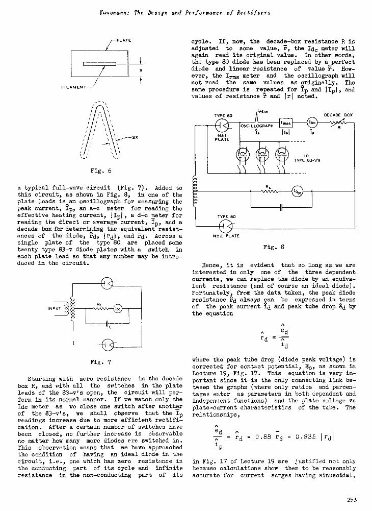
Kauzmann: The Design and Performance of Rectifiers
Fig. 6
a typical full -wave circuit (Fig. 7). Added tothis circuit, as shown in Fig. 8, in one of theplate leads is,an oscillograph for measuring thepeak current, Ip, an a -c meter for reading theeffective heating current, 1'0, a d -c meter forreading the direct or average current, Ip, and adecade box for determining the equivalent resist-ances of the diode, rd, Irdl, and rd. Across asingle plate of the type 80 are placed sometwenty type 83-v diode plates with a switch ineach plate lead so that any number may be intro-duced in the circuit.
Fig. 7
Starting with zero resistance in the decadebox R, and with all the switches in the plateleads of the 83-v's open, the circuit will per-form in its normal manner. If we watch only theIdc meter as we close one switch after anotherof the 83-v's, we shall observe that the Ipreadings increase due to more efficient rectifi-cation. After a certain number of switches havebeen closed, no further increase is observableno matter how many more diodes ere switched in.This observation means that we have approachedthe condition of having an ideal diode in thecircuit, i.e., one which has zero resistance inthe conducting part of its cycle and infiniteresistance in the non -conducting part of its
cycle. If, now, the decade -box resistance R isadjusted to some value, F., the Idc meter willagain read its original value. In other words,the type 80 diode has been replaced by a perfectdiode and linear resistance of value r. How-ever, the Inns meter and the oscillograph willnot read the same values as originally. Thesame procedure is repeated for Ip and IIpl, andvalues of resistance T. and Irl noted.
N'2 PLATE
Fig. 8
Hence, it is evident that so long as we areinterested in only one of the three dependentcurrents, we can replace the diode by an equiva-lent resistance (and of course an ideal diode).Fortunately, from the data taken, the peak dioderesistance rd always can be expressed in termsof the peak current id and peak tube drop ed bythe equation
A
A edrd = -77-
1d
where the peak tube drop (diode peak voltage) iscorrected for contact potential, E0, as shown inLecture 19, Fig. 17. This equation is very im-portant since it is the only connecting link be-tween the graphs (where only ratios and percen-tages enter as parameters in both dependent andindependent functions) and the plate voltage vsplate -current characteristics of the tube. The
relationships,
A
ed A -.
-7- . rd = 0.88 rd = 0.935 Irdi
ip
in Fig. 17 of Lecture 19 are justified not onlybecause calculations show them to be reasonablyaccurate for current surges having sinusoidal,
253
Vacuum Tube Design
triangular, and semicircular wave shapes. Forexample, in the equation rd = C id, determina-tion of the constant C for the different waveshapes gave values between 0.84 and 0.89. Thevalue of 0.88 shown in the relationships was de-rived for a sine wave and is applicable in mostcases to wave shapes usually encountered.
Obviously, just replacing the actual diode byan ideal diode and an equivalent series resist-ance does not take into account the effect ofexternal resistance present in the supply lineand transformers, or of the series resistancepurposely inserted in some close -spaced recti-fier circuits to prevent sputter on switching.This external resistance is purely ohmic, and isadded to the equivalent diode resistance directlyin each case (see Fig. 17, Lecture 19). For atransformer, the external resistance in ahalf-wave circuit is
RS =8'2 prim t see
where a = transformation ratio
Esec, read at no load.
Eprim
In the case of a full -wave rectifying trans-former, Rsec and Esec are for only half of fullsecondary windings.
PLATE DISSIPATION
The total heat dissipated by the plate of arectifier consists of that radiated by the cath-ode (which for practical purposes may be consid-ered as entirely surrounded by the plate) and thatgenerated at the plate as a result of the platecurrent through the diode. The heat radiated bythe cathode is easily determined by the equation
Wfil = Ef X Ifwhere
Wfil = filament or heater power in wattsEf = filament or heater voltsIf = filament or heater amperes
The plate -current dissipation can be experi-mentally determined by observing the envelopetemperature under the desired operating condi-tion and duplicating this temperature with d -cvoltage applied to the plate. This method isinconvenient and does not allow of prediction ofthe dissipation of a tube before it is made.
Another method, which is extremely tedious,is to take two simultaneous oscillographs of theactual tube voltage drop and the conducting cur-rent during the conduction period. The simul-taneous ordinates of voltage and current aremultiplied together to give instantaneous wattsoutput vs time. The area under the resultantcurve is then integrated over a full period toobtain the average dissipation. This method was
successfully used to check within 5 per cent theresults of the following two methods.
By use of the upper chart of Fig. 21 in Lec-ture 19, we can compute the dissipation. Atypical example will be given later in the lec-ture. Considerable error is possible unlessgreat care is used in interpolating the valuefor % IRS of RL. By this method, the plate dis-sipation is
Watteper plate = lIp12 x Irdi
The last method, and the one most convenientto use, is the result of assuming that the cur-rent pulse is sinusoidal in shape. Mathemati-cally this is not true but practically the ap-proximation is close, the error being probablyless than 5 per cent based on comparison with theoscillograph method. Under this assumption, theplate dissipation is
Wattsperplate
= 0.84 edIPper plate
whereed = diode peak voltage drop during conduct-
ing period.
The value of gd is obtained from the lower chartof Fig. 21 in Lecture 19, or where applicablefrom Fig. 9 byfirst obtaining the peak current,and then from the proper diode characteristic inFig. 5 obtaining the corresponding ed.
SIMPLIFICATIONS WHEN INPUT CONDENSER IS LARGE
1. Peak Currents
If we inspect Figs. 18, 19, and 20 in Lec-ture 19, which show the relationship between out-put voltage and wCRL, we notice that as &JCR', be-comes large all the curves of Rs (representingvarious diodes) flatten. In other words, if weincrease the value of the input condenser C, theoutput voltage becomes constant, and since EL isfixed, the output current, Ip = E/RL becomes con-stant. Similarly, from the lower chart of Fig.21 (Lecture 19), we notice that the peak -current -to -average -current ratios also become constantas we increase the value of C. Stated in otherWords, if we choose a filter condenser largeenough, the peak current, output voltage, andoutput current no longer are a function of thecondenser size. The data of these curves havebeen replotted in Fig. 9 where the current ratioIp/Ip per plate is shown plotted against the percent voltage ratio Err--max per plate. For mostreceiving -set rectifiers, a suitable value of Cis 16 in a full -wave circuit and 32 of in ahalf -wave circuit. These values are for maximumrated output of the rectifier tube.
2. Dissipation
If we continue along the above line of rea-
254
OWE EU
.12",41112"'A! =BM
an r
6. I In
!L
..... .. rouTss
ER
- -
- -
;
: II
; -
.:a
f
Z
Is - :
" :
-a
Z
- : :
;
" a
:
II
.
:
- - I
0 - .
. -
-
-
.
I
II .
:
:
Z -
a - .
th '0 1
- - : : Z
- I ...
: -
a II -
a - . III si -
- - : " -
I
II -
1 - -
II: - - ;: I II
II II,"
-
. - - ; - a
I . - I: ; :
- X11a
- I . Ir II
- :
:
$
A 5 5
I .
6
II

Vacuum Tube Design
1. Peak Current Determination
With entries of wCRL = 5.28 and % (E/ 'EMax) =71 %, we locate point A on Fig. 19 (Lecture 19)and obtain
whence
SinceRs = 11% x 3500 = 385 ohms,
RS = RS 1d
where Rs is the external series resistance of thetransformer and equals 33 ohms, we have from Fig.17 (Lecture 19)
rd = 385 - 33 = 352 ohms
rd = 0.85 rd = 0.88 x 352 = 310 ohms
IrdI = rd/0.935 = 332 ohms
RS = Rsrd= 33 + 310 = 343 ohms
a 11S 343- = x 100 = 9.8%
RL 3500
% S =9.8 %
nRI, 2
Now we can obtain the ratio of peak currentto d -c plate current from the lower chart ofFig. 21 (Lecture 19). Using as entries nwCRL =10.5 and % (RS/nRL) = 4.9 %, we locate point B,and obtain
= 6.2
Ip per plate
Therefore,
Ip = 6.2 x 114 = 354 milliamperes2
2. Total Dissipation
a) By equation:
Wattsperplate
= 0.84 ed Tp per plate
Since in = 354 milliamperes, and from curveH of Fig. 5 showing the diode characteristic ofthe 5W4, we obtain
ed = 109 voltsTherefore,
Wattsper plate = 0.84 x 109 x (0.114/2) = 5.2
we have
and
and the total dissipation is the sum of the platewatts (Wp) and the filament watts (Wf) or
Wp Wf = 2(5.2) (5 x 2) = 20.4 watts *
b) By equation: Wattsper plate = IIp12 Irdi
Since we have found the value of Irdl to
be 332 ohms, and if we add the transformer re-sistance Rs = 33 ohms, then from the equation
1%1 = Rs + Irdl
IRsI = 33 + 332 = 365 ohms
ORsI= 365 x 100 = 5.2%nRI, 2 x 3500
Using as entries
nWCRL = 10.5 and % (IRsI)/ nRL = 5.2%
we locate point C on the upper chart of Fig. 21(Lecture 19) and obtain
Therefore,
Ilpl= 2.2
ip per plate
IIpl = 2.2 x114
2
= 125.5 rms milliamperes equivalentHence,
Wattsper plate = (0.1255)2 x 332 = 5.2
and the total dissipation is
Wp Wf = 2(5.2) 10 = 20.4 watts *
DESIGN OF A RECTIFIER FOR A GIVENOUTPUT CURRENT
The problem is to design a full -wave recti-fier to operate at 400 volts rms per plate, andto supply an output current of 200 milliamperesat an output voltage of not less than 400 voltsd.c. The filter is to be of the condenser -inputtype, and it will be assumed that the size ofthe condenser will be large, i.e., 30 µf orgreater. This assumption greatly simplifies thework.
* This dissipation is not safe for the 5W4 be-cause its MT8G envelope has amaximum dissipationlimited to 19.7 watts.
256
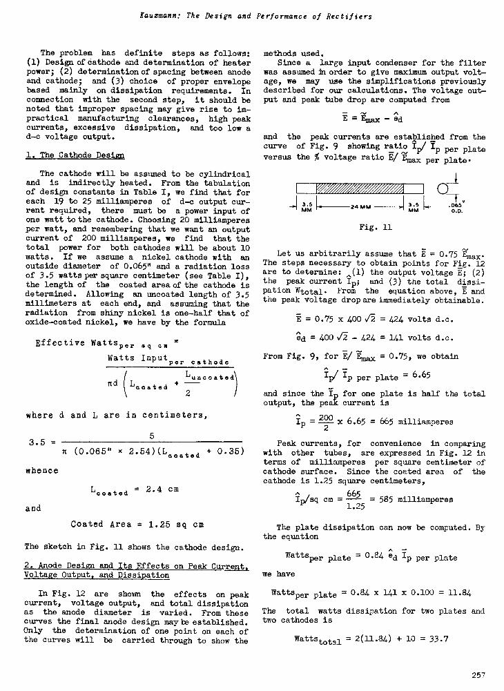
Kauzmann: The Design and Performance of Rectifiers
The problem has definite steps as follows:(1) Desigaofeathode and determination of heaterpower; (2) determinatiaaofspacing between anodeand cathode; and (3) choice of proper envelopebased mainly on dissipation requirements. Inconnection with the second step, it should benoted that improper spacing may give rise to im-practical manufacturing clearances, high peakcurrents, excessive dissipation, and too low ad -c voltage output.
1. The Cathode Design
The cathode will be assumed to be cylindricaland is indirectly heated. From the tabulationof design constants in Table I, we find that foreach 19 to 25 milliamperes of d -c output cur-rent required, there must be a power input ofone watt to the cathode. Choosing 20 milliamperesper watt, and remembering that we want an outputcurrent of 200 milliamperes, we find that thetotal power for both cathodes will be about 10watts. If we assume a nickel cathode with anoutside diameter of 0.065" and a radiation lossof 3.5 watts per square centimeter (see Table I),the length of the coated area of the cathode isdetermined. Allowing an uncoated length of 3.5millimeters at each end, and assuming that theradiation from shiny nickel is one-half that ofoxide -coated nickel, we have by the formula
Effective Wattsper sq cm =
Watts Inputper cathode
nd (Lcoated 4-
Luncoated
2
where d and L are in centimeters,
3.5 =
whence
and
5
n (0.065" = 2.54)(L...ted 0.35)
Lcoated = 2.4 cm
Coated Area = 1.25 sq cm
The sketch in Fig. 11 shows the cathode design.
2. Anode Design and Its Effects on Peak Current.Voltage Output, and Dissipation
In Fig. 12 are shown the effects on peakcurrent, voltage output, and total dissipationas the anode diameter is varied. From thesecurves the final anode design maybe established.Only the determination of one point on each ofthe curves will be carried through to show the
MM
methods used.Since a large input condenser for the filter
was assumed in order to give maximum output volt-age, we may use the simplifications previouslydescribed for our calculations. The voltage out-put and peak tube drop are computed from
E = Emax - ed
and the peak currents are established from thecurve of Fig. 9 showing ratio Ip/ Ip per plateversus the % voltage ratio E/ Emax per plate.
3.5 1_, 24MM
Fig. 11
pN-1
3.5 .065MM 0.D.
Let us arbitrarily assume that E = 0.75 Emax.The steps necessary to obtain points for Fig. 12are to determine: ,(1) the output voltage E; (2)
the peak current Ip; and (3) the total dissi-pation Wtotal. From the equation above, E andthe peak voltage drop are immediately obtainable.
E = 0.75 x 004. = 424 volts d.c.
ed = 400,5 - 424 = 141 volts d.c.
From Fig. 9, for E/ Lax = 0.75, we obtain
_Ip/ Ip per plate . 6.65
and since the ip for one plate is half the totaloutput, the peak current is
IP
= 200 6.65 = 665 milliamperes
Peak currents, for convenience in comparingwith other tubes, are expressed in Fig. 12 interms of milliamperes per square centimeter ofcathode surface. Since the coated area of the
cathode is 1.25 square centimeters,
ip/sq cm =.§±.2 = 585 milliamperes1.25
The plate dissipation can now be computed. Bythe equation
Wattsper plate = O.84 ed Ip per plate
we have
Wattsper plate = 0.84 x 141 x 0.100 = 11.84
The total watts dissipation for two plates andtwo cathodes is
Wattstotal = 2(11.84) + 10 = 33.7
257
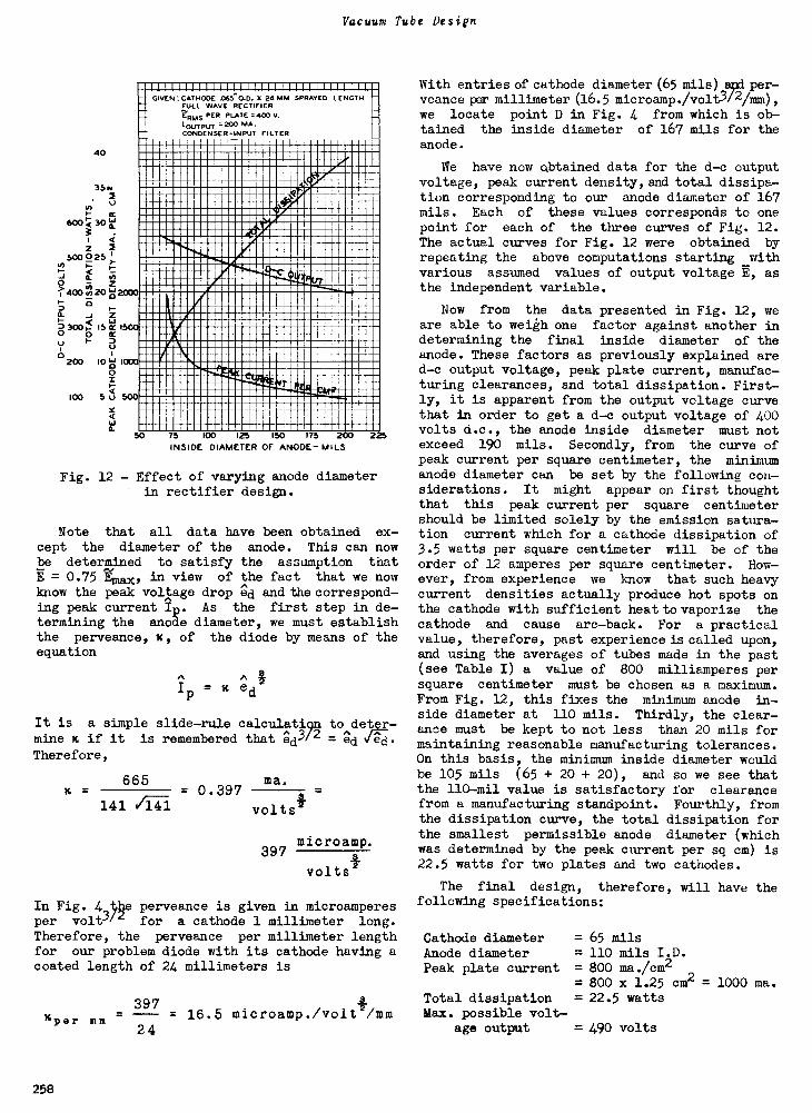
Vacuum Tube Design
40
35m2um
600 7( 30 le
¢2
500 0 250-1
<a 0
0 - Z> w400 cr0i 20 at -
_J ZD 300 F.-< 15K IS0 m
M
X200 10t1 1
0
100 5 u 500
a.
II I 11111111111111111 III IIIIIgm ...=me III
...._,,!
EI w1 MM114%,
. II
U.immommimmommummums'Am ismMEMMEMMEOMMEMMEME KAM 111 =MN1111111111111,111e1111 III=r4rnommllminommommummormsomm..mmomhzegummingdmmom Email!1111111164141,511111
ilimmummemniaLfmanime millmmommErammokammag.., JummummaimmummizauseA rum
-.111111111:111111111111111 gustunnummer.onm. ...miummirammumammumminsiimm
..11111.111111111111111111117777:
mEmoMomEmmm=s MliEa m
ow mommummommAllaP11,1111111i iii I
IIIIIIIiiialrl milli
PAMIEMNIP RILINIA MMMMEMMOOWWI WMIMIMOMIIMMEMOBIMO
II I I II I 1 I 1.1 I I I II I 1 l I 1 1 1 1
GIVEN:CATHODE .065 0.D. 2 24 NW SPRAYED LENGTHFULL WAVE RECTIFIERERMS PER PLATE .400 V.'OUTPUT '2°° MA.CONDENSER -INPUT FILTER
-r
75 100 125 150 175 200 225INSIDE DIAMETER OF ANODE- M L5
Fig. 12 - Effect of varying anode diameterin rectifier design.
Note that all data have been obtained ex-cept the diameter of the anode. This can nowbe determined to satisfy the assumption thatE = 0.75 Emax, in view of the fact that we nowknow the peak voltage drop gd and the correspond-ing peak current Ip. As the first step in de-termining the anode diameter, we must establishthe perveance, x, of the diode by means of theequation
Ip = x ;d1
It is a simple slide -rule calculati9n to det;gr -mine x if it is remembered that ed3'2 = gd Jed.
Therefore,
665x = = 0.397
ma.
141 4 volts
397microamp.
volts*
In Fig. 4 he perveance is given in microamperesper volt3'2 for a cathode 1 millimeter long.Therefore, the perveance per millimeter lengthfor our problem diode with its cathode having acoated length of 24 millimeters is
xper mm =397
= 16.5 microamp./volt2/mm24
With entries of cathode diameter (65 mils) per-veanceper millimeter (16.5 microamp./volt3/2and/mm),we locate point D in Fig. 4 from which is ob-tained the inside diameter of 167 mils for theanode.
We have now obtained data for the d -c outputvoltage, peak current density, and total dissipa-tion corresponding to our anode diameter of 167mils. Each of these values corresponds to onepoint for each of the three curves of Fig. 12.The actual curves for Fig. 12 were obtained byrepeating the above computations starting withvarious assumed values of output voltage E, asthe independent variable.
Now from the data presented in Fig. 12, weare able to weigh one factor against another indetermining the final inside diameter of theanode. These factors as previously explained ared -c output voltage, peak plate current, manufac-turing clearances, and total dissipation. First-ly, it is apparent from the output voltage curvethat in order to get a d -c output voltage of 400volts d.c., the anode inside diameter must notexceed 190 mils. Secondly, from the curve ofpeak current per squnre centimeter, the minimumanode diameter can be set by the following con-siderations. It might appear on first thoughtthat this peak current per square centimetershould be limited solely by the emission satura-tion current which for a cathode dissipation of3.5 watts per square centimeter will be of theorder of 12 amperes per square centimeter. How-ever, from experience we know that such heavycurrent densities actually produce hot spots onthe cathode with sufficient heat to vaporize thecathode and cause arc -back. For a practicalvalue, therefore, past experience is called upon,and using the averages of tubes made in the past(see Table I) a value of 800 milliamperes persquare centimeter must be chosen as a maximum.From Fig. 12, this fixes the minimum anode in-side diameter at 110 mils. Thirdly, the clear-ance must be kept to not less than 20 mils formaintaining reasonable manufacturing tolerances.On this basis, the minimum inside diameter wouldbe 105 mils (65 + 20 + 20), and so we see thatthe 110 -mil value is satisfactory for clearancefrom a manufacturing standpoint. Fourthly, fromthe dissipation curve, the total dissipation forthe smallest permissible anode diameter (whichwas determined by the peak current per sq cm) is22.5 watts for two plates and two cathodes.
The final design, therefore, will have thefollowing specifications:
Cathode diameterAnode diameterPeak plate current
= 65 mils
= 800 ma./cm2= 800 x 1.25 cm2 = 1000
Total dissipation =Max. possible volt-
age output
22.5 watts
490 volts
ma.
258
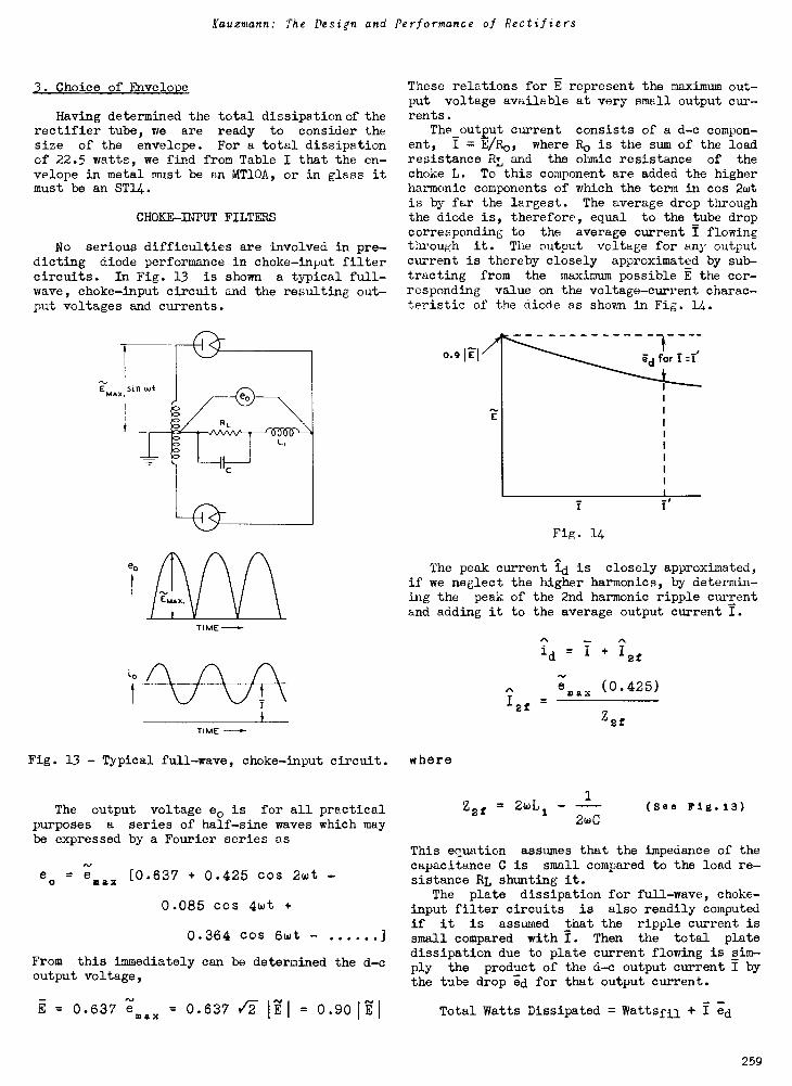
Kauzmann: The Design and Performance of Rectifiers
3. Choice of Envelope
Having determined the total dissipation of therectifier tube, we are ready to consider thesize of the envelope. For a total dissipationof 22.5 watts, we find from Table I that the en-velope in metal must be an MT10A, or in glass itmust be an STJ4.
CHOKE -INPUT FILTERS
No serious difficulties are involved in pre-dicting diode performance in choke -input filtercircuits. In Fig. 13 is shown a typical full -wave, choke -input circuit and the resulting out-put voltages and currents.
TIME
TIME
Fig. 13 - Typical full -wave, choke -input circuit.
The output voltage e0 is for all practicalpurposes a series of half -sine waves which maybe expressed by a Fourier series as
eo = emax [0.637 + 0.425 cos 2wt -
0.085 cos 4wt
0.364 cos 6wt - j
From this immediately can be determined the d -coutput voltage,
= 0.637 ;max = 0.637 / Itl = 0.90
These relations for E represent the maximum out-put voltage available at very small output cur-rents.
The output current consists of a d -c compon-ent, I = E/Ro, where R0 is the sum of the loadresistance RL and the ohmic resistance of thechoke L. To this component are added the higherharmonic components of which the term in cos 2wtis by far the largest. The average drop throughthe diode is, therefore, equal to the tube dropcorresponding to the average current I flowingthrough it. The output voltage for any outputcurrent is thereby closely approximated by sub-tracting from the maximum possible E the cor-responding value on the voltage -current charac-teristic of the diode as shown in Fig. 14.
0.9IEI
E
for I
Fig. 14
The peak current id is closely approximated,if we neglect the higher harmonics, by determin-ing the peak of the 2nd harmonic ripple currentand adding it to the average output current I.
where
- ^id = I + I2f
2f -
ems. (0.425)
Zee
Z2f = 2wL1 - 1 (See F1g.13)
This equation assumes that the impedance of thecapacitance C is small compared to the load re-sistance RL shunting it.
The plate dissipation for full -wave, choke -
input filter circuits is also readily computedif it is assumed that the ripple current issmall compared with I. Then the total plate
dissipation due to plate current flowing is sim-ply the product of the d -c output current I bythe tube drop ed for that output current.
Total Watts Dissipated = Wattsfil + I ;d.
259

Vacuum Tube Design
RIPPLE VOLTAGE
The ripple voltage with which we are concernedis that appearing directly after the tube.
For condenser -input filters, the frequency ofthis ripple is the same as that of the supplyvoltage for half -wave circuits, and is twice thesupply frequency for full -wave and voltage -doubler circuits. Fig. 22 in Lecture 19 evalu-ates the ripple voltage in terms of parameterscontaining equivalent tube resistance, condenserfilter, and load resistance.
For full -wave, choke -input circuits, the rip-ple -voltage frequency is twice the supply fre-
quency, and is approximately equal to the 2ndterm of the Fourier series shown in the preced-ing section on Choke -Input Filters.
e2f max (0.425 cos 2wt)
This may be further corrected by subtracting thetube drop corresponding to a plate current equalto the output current I.
Table I
e2f = amax - ed)(0.425 cos 2wt)
EMPIRICAL DESIGN DATA FOR RECTIFIERS
This table has been prepared from data on 16 types of RCA rectifiers, mostly for receiving -setapplications. In the case of watts per square centimeter radiated from the cathode, conductionlosses were lumped with the radiation losses by assuming that the radiation per square centimeterfrom the uncoated portions was one half that for the coated portions of the cathode.
ITEM FILAMENTTYPE *
CLOSE -SPACEDINDIRECTLY HEATEDCATHODE TYPE
MERCURY-VAPORCOATED -FILAMENT
TYPE **UNITS
Cathode Radiationper sq cm 3.5 - 4.0 3.5 4.6 - 4.7 Watts
D -C Output Currentper watt input tofilament or heater
17 - 25 19 - 25 17 Milliamperes
Peak Currentper watt input tofilament or heater
100 - 175 170 - 200 150 Milliamperes
D -C Output Currentper sq cm ofcathode surface
70 - 90 70 - 100 80 - 90 Milliamperes
Peak Currentper sq cm ofcathode surface
400 - 600 600 - 800 700 Milliamperes
* With No.16 alloy filament * 2500 volts (rms) per plate max. applied voltage
ITEM METAL SHELL S ° GLASS BULBS 00 UNITS
Envelope MT8K MT8G MT8B MT10A ST12 ST14 ST16 # -
Dissipation 7.8 14.5 19.7 35.0 16.5 23.5 41 Maximum Watts
Values are on basis of 2.5 watts per sq. in. Above this value, the paint on the shell burns.00 Values are on basis that getter flash is small and confined to bottom of bulb.# With No.814KW glass stem. When the ST16 bulb is used for full -wave, mercury-vapor tubes with
550 volts rms per plate, the effective dissipation is decreased to about 17.5 watts dependingon the ambient temperature. This limitation is necessary to prevent arc -back under conditionswhere only natural cooling is used.
260