UWB Antenna
114
UWB Antenna Design for Polarimetric Imaging Radar MASTER OF SCIENCE IN ELECTRICAL ENGINEERING AT DELFT UNIVERSITY OF TECHNOLOGY Name Syeda Nadia Haider Student No. 1369768 Supervisors Prof. dr. A. G. Yarovoy Yu Che Yang MICROWAVE TECHNOLOGY AND SYSTEMS FOR RADAR DEPARTMENT- TELLECOMMUNICATIONS DELFT UNIVERSITY OF TECHNOLOGY
-
Upload
baskarakasi -
Category
Documents
-
view
386 -
download
5
Transcript of UWB Antenna

UWB Antenna Design for Polarimetric
Imaging Radar
MASTER OF SCIENCE IN ELECTRICAL ENGINEERING
AT
DELFT UNIVERSITY OF TECHNOLOGY
Name Syeda Nadia Haider
Student No. 1369768
Supervisors Prof. dr. A. G. Yarovoy
Yu Che Yang
MICROWAVE TECHNOLOGY AND SYSTEMS FOR RADAR
DEPARTMENT- TELLECOMMUNICATIONS
DELFT UNIVERSITY OF TECHNOLOGY


UWB Antenna Design for Polarimetric
Imaging Radar
By
Syeda Nadia Haider
Student, Master of Science (Telecommunications), IRCTR
Abstract
Imaging radar has become a keen research topic in recent years. UWB technology provides many
advantages to imaging radar such as fine resolution and high power efficiency. The performance
of a UWB imaging radar can be further improved by applying polarimetric diversity. The
polarimetric signature of objects can be used to enhance the quality of target recognition. Like
any other wireless systems, antennas are key factors of radar systems. The focus of this thesis is
to develop a dual polarized antenna for UWB imaging radar. Comparative study of six different
UWB antenna types is performed. It is concluded that the X-band UWB antenna recently
developed at IRCTR has most potential for this project. The antenna element was optimized for
the Ku-band and an impedance bandwidth from 8 GHz to 24 GHz was achieved. An orthogonal
coax-to-coplanar transition has been developed during this project and this transition is used to
feed the antenna element. The antenna elements are successfully applied in two different array
configurations. It is demonstrated that these sub-arrays have over 100% fractional bandwidth,
good impedance matching, linear phase (almost constant group delay) and uni-directional pattern.
These aspects collectively account for the novelty in design. In future, these sub-arrays will be
implemented inside a complete array structure of UWB imaging radar.
Supervisor Professors: Prof. dr. A. G. Yarovoy
Supervisor: B. Yang


Acknowledgement
I would like to express my sincere gratitude to my supervisor, Professor A. G. Yarovoy for his advice and
encouragement. His deep understanding and immense knowledge helped me solve many difficult
problems. He guided me throughout this project, even during his extremely busy schedule. I am also
grateful to my supervisor, Yu Che Yang for his support and supervision. A special acknowledgement goes
to D. P. Tran for his enthusiasm, his help to solve many practical problems and his patience to answer my
many questions.
I extend my thanks to IRCTR for providing me with such a great opportunity. This master thesis project
has been a very valuable learning experience. It has given me the chance to learn better ways of achieving
goals from more experienced personnel. Above all, the most important asset I have taken from this
experience is the willingness to learn. The working atmosphere and especially the nice persons of this
department have encouraged me in my work. I would like to thank them all for their hospitality. My
sincerest thanks go to all my teachers and friends who have shaped my life in various ways. Special thanks
to Ben van Zon, who guided me during my undergraduate research project at Nedap, for helping me to
develop my first interest in antenna design. Thanks to my fiancé Bas Tijs for supporting me throughout
my master study. Last but not least to my parents and sisters, I extend my deepest love. They have always
motivated me to continue my higher studies.


Table of Contents
1 Introduction 1
1.1 Research problem 2
1.2 Objective of the thesis 2
1.3 Challenges in UWB antenna design 3
1.4 Novelties of the work and approach 4
1.5 Thesis organization 4
2 Comparative Analysis of Different Antenna Types 6
2.1 Introduction 6
2.2 Planar spiral antenna 6
2.3 Helical antenna 8
2.4 Stacked microstrip antenna 9
2.5 Dual orthogonal polarized UWB antenna 10
2.6 Cross bowtie antenna 13
2.7 Tran antenna 15
2.8 Comparison of antennas 18
2.9 Conclusions 19
3 Dual Orthogonal Polarization with an Array Structure 20
3.1 Introduction 20
3.2 Criteria for the dual polarization 20
3.3 Two approaches for dual orthogonal polarization generation 22
3.4 Dual polarization with linearly polarized elements 23
3.5 Conclusions 28
4 Antenna Element for 8 to 24 GHz Frequency Band 29
4.1 Introduction 29
4.2 Scale factor 30
4.3 Parametric study 31
4.4 Analysis of the 8 to 24GHz antenna element 34
4.5 Conclusions 38

5 Wideband Perpendicular Coax-to-coplanar Transition 39
5.1 Introduction 39
5.2 The perpendicular transition design 41
5.3 The truncated crown of vias 43
5.4 The parametric study of the pad diameter and position 48
5.5 Conclusions 53
6 The Antenna Array Design 54
6.1 Introduction 54
6.2 The conventional array structure 55
6.2.1 The initial topology of the conventional array 55
6.2.2 Miniaturizing the sub-array 60
6.3 The Huang array structure 73
6.3.1 The initial topology of the conventional array 73
6.3.2 Element spacing vs. cross polarization for the Huang array 76
6.4 Dual orthogonal polarized array structure for 8 – 24 GHz 83
6.5 Fabrication 89
6.6 Conclusions 90
7 Conclusions and Recommendations 91
Appendix A: Some Additional Simulations 94
Appendix B: Selection of the Electromagnetic Solver 102
Bibliography 104


Chapter 1: Introduction
1
Chapter 1
1 Introduction
Radar systems use electromagnetic wave to detect and identify targets. Most conventional radar operates
in a relative narrow band. Harmonics or sinusoidal signals are used as transmit signal. These narrow band
radar systems are capable of target detection and tracking but target imaging is beyond their capability due
to the insufficient bandwidth. Therefore, recently numerous research works have been carried out to
improve bandwidth of radar systems and use UWB signals for target imaging. Widening the bandwidth
will translate into high spatial resolution which will help to distinguish between closely spaced targets or
targets from background clutters. Besides, UWB radar provides low probability of interception, better
target information recovery, non-interfering waveform and opportunity to perform time analysis [1].
Examples of UWB imaging are the through-wall imaging radar and through-dress imaging radar [2,3,4].
These imaging radars have become an important research topic in the recent years. The through wall
imaging radar provides the law enforcement officers enhanced situation awareness in urban warfare or
hostage rescue scenarios. This radar system is also of great interest for earthquake rescue or determining
the position of people inside a smoky building. Through dress imaging (TDI) radar are used to detect
concealed weapon in protected areas. The signal attenuation through wall or cloth can be higher at specific
frequency bands. In general the transmission losses for different frequencies are not a priori knowledge
and therefore ultra wideband signal are often used. This ensures that at least some part of the frequency
band will get through the wall and radar will be able to detect the target reflected signal. Moreover, UWB
technology has the ability to resolve multipath delay in nanosecond range. To avoid interference, the time
window of observation can be adjusted based on the expected time of arrival of the wanted signal. Besides
the above mentioned scenarios, the UWB imaging has been also found to be a useful tool for early breast
cancer detection [5] and for ground penetrating radar (GPR) [6].

Chapter 1: Introduction
2
1.1 Research problem
Traditional radars measure amplitude, phase and frequency shift of the reflected wave. These parameters
are used to detect a target or to determine the velocity of a moving target. However, these radar systems
only use scalar wave description and do not make a full use of the properties of the electromagnetic field
which is a vector by nature [7]. Polarimetric radar utilizes this electormagnetic field property. It transmits
and receives both horizontal and vertical pulses. While linear polarization can be used to estimate the size
and the distance of a scatter, dual or circular polarization can in addition help to determine the shape and
the orientation of the target.
Furthermore, if same polarization is used for the transmit and receive antenna (either both horizontal or
both vertical), it does not mean that the system is receiving the total scattered field. This is because when
an EM wave incidents upon an object, the object transforms the incident wave into a scattered wave and
during this transformation the polarization state of the wave may change. Consequently, a linearly
polarized radar system is only able to retrieve a portion of the reflected wave.
Polarimetry is an essential feature for radar systems. On the other hand, UWB has been shown as a useful
feature of the radar too, which provides higher resolution and thus also helps with target classification. It
is a very attractive idea to combine these both features (polarimetry and UWB) into the same system and
benefit from both in the target classification. However, there are a number of difficulties here. One of
them is the absence of dual-polarized UWB antennas.
1.2 Objective of the thesis
Several UWB imaging systems have been recently developed at IRCTR. These systems are not using
polarimetric data. Polarimetric diversity will provide more complete description of targets. Specific
polarization signature of some object can be used for the recognition of its shape and this will enhance
target classification. Therefore, the main goal of this project is to develop dual or circularly polarized
UWB antenna for high resolution imaging.
The second important requirement for this antenna is a uni-directional radiation pattern (front-to-back
ratio more than 10 dB). In future state the antenna element is intended to be used in an array structure.
Therefore a uni-directional pattern is needed to maximize the forward gain and to shield the antenna from

Chapter 1: Introduction
3
the electronics mounted on the back side. Besides, this antenna should cover large portion of the X and
Ku-band. In this band a good impedance matching is required which means return loss below -10dB.
Stable radiation pattern should be observed within this band. The main lobe of the pattern should be in the
broad side direction, the side lobe levels should be low and good radiation efficiency is important.
Regarding the antenna structure, a planar antenna is more preferable to simplify the implementation of the
elements in an array. In addition, the required area of the elements should be small enough to fit within the
allowable element spacing. Roughly the size needs to be half of the free-space wavelength at the center
frequency. The gain of each element should be at least positive in the operating frequency band and the
beamwidth should be at least 30° in both E and H planes to illuminate sufficient area. Moreover, the
antenna should have a suitable time domain behavior with low group delay and ringing.
1.3 Challenges in UWB antenna design
There are many definitions of an antenna. An antenna is defined by Webster’s Dictionary as “a usually
metallic device for radiating or receiving radio waves”. The IEEE standard Definitions of Terms for
Antennas defines the antenna as “That part of a transmitting or receiving system which is designed to
radiate or to receive electromagnetic waves”. Another commonly used definition is “A transition structure
between a guiding device and the free space”. Ultra wideband (UWB) antenna is defined as an antenna
with a fractional bandwidth larger that 20% or absolute bandwidth (LOUP ff − ) larger than 500 MHz. The
fractional bandwidth is defined as the ratio of the absolute bandwidth to the centre frequency
CLOUPfract ffff /)( −=∆ . The centre frequency is either the arithmetic average of the upper and lower
frequencies, 2/)( LOUPC fff += or the geometric averageLOUPC fff = .
An antenna plays a very crucial role in narrowband as well as UWB systems. However, designing an
antenna for UWB application has additional challenges. An UWB antenna must be able to receive or
transmit an extensively large range of frequencies at a same time and therefore the antenna performance
should be satisfactory throughout the operational band. The antenna must provide a good impedance
match which correspond to voltage standing wave ratio (VSWR) less than 2 over the entire band. Apart
from obtaining a sufficient impedance bandwidth, a non-dispersive behavior is also required for optimal
wave reception and transmission. A non-dispersive behavior is achieved by maintaining a linear phase

Chapter 1: Introduction
4
which corresponds to constant group delay. However, in practice if the group delay is near constant and
the changes occur in a predicated manner, provides acceptable pulse characteristics.
Aside from these requirements, the radiation pattern should be also consistent throughout the bandwidth.
To achieve a wide impedance bandwidth and still maintain high radiation efficiency is one of the main
challenges in UWB antenna design. Simple antennas, such as the finite-length dipole, are not capable of
maintaining constant characteristics over wide bandwidths. More sophisticated antenna structures are
needed to meet these requirements.
1.4 Novelties of the work and approach
During this thesis project, two possibilities of a dual-polarized antenna design have been foreseen: a single
antenna with possibility to activate one of two orthogonal polarizations and a full-poalrimetric sub array
with linearly polarized elements. Finally, an UWB antenna is used in an array structure for dual
polarization , which is a novel approach. Two different types of arrays are used: the conventional array
configuration and the Huang array configuration. Both of these array structures are able to acquire an
extremely wideband, uni-directional patter, sub-nano second group delay and good radiation
characteristics. These two array configurations account for the novelty in the design. Further, the novelty
of this thesis lies also in the design of the orthogonal coax-to-coplanar antenna feeding for the antenna
elements, optimization of the antenna element within the array and optimization of the complete sub-
array. Finally, a new antenna design for Ku-band has been made.
1.5 Thesis organization
This thesis is organized in seven chapters as follows:
Chapter 2: After this introduction to the objective of this thesis, a comparative study of different
candidate antennas is followed. The advantages and disadvantages of these antennas are presented in this
chapter. This comparative study is based on recent publications and the simulation results.
Chapter 3: In this chapter the basic concept of the dual orthogonal polarization is pointed out. Followed
by advantages of using an array, two different array types are presented. Furthermore, the basic concept of
one of these arrays, the Huang array is clarified.

Chapter 1: Introduction
5
Chapter 4: This chapter is devoted to the design of an antenna element for 8 to 24 GHz frequency band.
Here the simulated model, the scaling effect and the parametric study of this antenna element are
presented.
Chapter 5: In this chapter the orthogonal coax-to-coplanar transition is evaluated. This chapter also
contains the explanation concerning the necessity of the back feeding technique, difficulty in realizing this
transition and the final outcome.
Chapter 6: The design of the dual polarized array with the linearly polarized elements is detailed in this
chapter. Simulation results are presented and the performance of different array structures is also
analyzed.
Chapter 7: This chapter concludes the researches that have been done during the thesis and summarizes
the final results. Recommendation for future work is also presented here.

Chapter 2: Comparative Analysis of Different Antenna Types
6
Chapter 2
2 Comparative Analysis of Different
Antenna Types
2.1 Introduction
Recently UWB antennas have received considerable attention in different fields due to their many
advantages over conventional narrow band antennas. A wide variety of antennas have been designed in
last ten years which are suitable for UWB applications. For this thesis project we need an antenna
structure which either radiates a circularly polarized field or dual orthogonal linear fields. A number of
antennas are considered as a candidate for this project. In this chapter a comparative study of these
antennas is presented.
2.2 Planar spiral antenna
Spiral antennas are one of the most commonly used UWB antennas when circular polarization is required.
A spiral antenna can provide a large bandwidth with relatively constant input impedance, antenna gain and
radiation pattern. The main cause of this wideband behavior is the travelling wave of the current which
propagates along the spiral arms and brings energy from the feed point into the radiation area. There are
two major types of spiral antenna: the logarithmic spiral [8] and the Archimedes spiral [9]. The shape of
the infinite logarithmic spiral can be determined only in term of the angle and therefore according to
Rumsey’s principle the impedance and the pattern properties of this antenna will be frequency-
independent. For a finite logarithmic spiral, the operational band is limited within the wavelength shorter
than the circumference and the wavelength greater than the diameter of the feed point. The Archimedes

Chapter 2: Comparative Analysis of Different Antenna Types
7
spiral is not regarded as a true frequency independent antenna. However, a tight Archimedes spiral is a
close approximation of a tightly wound logarithmic spiral and we can consider it as a frequency-
independent antenna.
Figure 2-1 Spiral antennas. Left: Logarithmic spiral, Right: Archimedes spiral
For a spiral antenna the lower and the upper cutoff frequencies are independent of each other. Upper
cutoff frequency is dependent on the fineness of the construction at the feed point and the lower cutoff
frequency is a function of the overall diameter. Typical gain of a planar spiral antenna is about 5 to 6 dBi.
The maximum diameter of a conventional spiral is one-third of the wavelength of the lowest frequency.
Size reduction of spiral can be achieved by material loading but this increases the material loss and the
weight. Slow wave spiral techniques can be used to minimize the size up to 16.6% (for examples, square
spiral and star spiral).
One of the major disadvantages of this antenna is its dispersive behavior. The higher frequency
components of the signal radiate near the spiral center and the lower frequency components radiate near
the end of the spiral arms (the radiated signal wavelength is equal to the spiral circumference). Therefore,
the higher frequency components radiate first and the group delay of the transmitted signal decreases with
the frequency. This causes signal dispersion. Furthermore, spiral antennas are bi-directional. To transform
the bi-directional beam to a unidirectional beam a ground plane or a cavity with absorbing strip can be
used. The disadvantage of an absorbed material is that only half of the input power will be radiated. On
the other hand, the antenna performance becomes highly frequency dependent when a floating ground
plane is used. The effect of a ground plane can be seen as a short circuited transmission line connected to
the antenna. The input impedance of the ground is in parallel with the antenna impedance. The frequency
for which the distance between the antenna and the ground plane is λ/4, there is a constructive interference

Chapter 2: Comparative Analysis of Different Antenna Types
8
Figure 2-2 Hellical antenna
between the incident wave and the wave reflected by the ground plane. For any other frequency this
interference will not be completely constructive and the reflection coefficient will increase.
2.3 Helical antenna
The axial mode helical antenna was first invented by John
Kraus at Ohio State University in 1964 [9]. This is a traveling
wave type antenna. The helical antenna consists of
conducting wire wound in the form of a screw on top of a
ground plane. The center conductor of the coaxial cable is
usually attached to the antenna and the outer conductor is
connected to the ground plane. For end-fire mode, the
circumference of the antenna has to be such that the phase
difference of current on two opposite side is half-wavelength.
Now due to the winding the field radiated from this two ends
will be in phase along the axis. The back radiation of a helical
antenna is very low if axial mode is used. The most important parameters of a helix are the beamwidth,
gain, impedance and axial ratio. These parameters of a helical antenna depends on various parameters:
wire radius, location of the feeding point, number of turn, pitch angle and the size of the conducting wire
near the feed. Generally antenna with thicker conductors gives better broadband performance for the same
antenna length and the bandwidth decreases slightly when the antenna length or the number of turns
increases [10]. The input impedance of the helix in the axial mode is nearly resistive over a wideband. The
number of turns of a helical antenna has a great influence on the axial ratio, beamwidth and directivity.
Axial ratio, 2 1
2
NAR
N
+= .
Half-power-beamwidth,
λλ NSCHPBW
052=
Directivity, λλ NSCD 212=
Here, N is the number of turns, λC and λS are in free-space wavelength the circumference and spacing
between two turns respectively. For a sufficient numbers of turns the axial ratio becomes almost one and

Chapter 2: Comparative Analysis of Different Antenna Types
9
the polarization becomes almost circular. From the above equation we can see that the beamwidth
decreases with the number of turns and on the other hand the directivity increases.
The main disadvantage of the helical antenna is its large dimension. As an example we can consider a 5-
turn helix at 6 GHz center frequency. If the antenna operates in axial mode then by using the above
equations we know that the axial ratio will be about 1.1 or 0.41 dB, half power beamwidth will be 48.4°
and directivity will be 12.4 dB.
The length of this antenna, L= 5*S (Here, S is the spacing between turns in mm)
=5*0.231* 0λ ( 0λ is wavelength for the center frequency)
=58 mm
Typically, the diameter of the antenna is 0 /λ π or about one-third of the free-space wavelength at the
center frequency but the diameter of the ground plane should be 4/3 0λ . Moreover, the length of this
antenna should be 0*16.1 λ . Above parameters indicate the large dimensions of this antenna.
2.4 Stacked microstrip antenna
A microstrip antenna is a low-profile antenna that has a number of advantages over other antennas – it is
lightweight, inexpensive and easy to integrate with accompanying electronics. Another advantage of a
patch antenna is the ability to have polarization diversity. Patch antenna can easily be designed to have
vertical, horizontal, right hand circular (RHCP) or left hand circular (LHCP) polarizations, using multiple
feed points or a single feed point with asymmetric patch structures. Moreover, a microstrip antenna is
relatively easy to design and simulate. Conventional microstrip antennas are resonance type antennas and
have narrow bandwidth. By using a parasitic element over a radiating patch, the antenna with wide
bandwidth can be realized [12]. These types of antennas are known as the stacked microstrip antenna.
Typically they have two patches (upper and lower patch) and the radiation is mainly due to the coupling
between these two patches. For an aperture stacked microstrip antenna the field is coupled from the
microstrip feed line to the radiating patch (other side of the ground plane) through an electrically small
slot in the ground plane. Multi-layer substrates with varying thickness are often used. Aperture coupled
configuration provides the advantage of isolating spurious feed radiation by use of a common ground. For
this type of antenna a front to back ratio of about 10 dB over the entire band can be achieved. The major
Chapter 2: Comparative Analysis of Different Antenna Types
10
disadvantage of stacked antenna is its limited bandwidth (maximum 70%). Moreover, if for dual or
circular polarization cross slot is used, this will cause additional 5 to 10% decrease in the bandwidth.
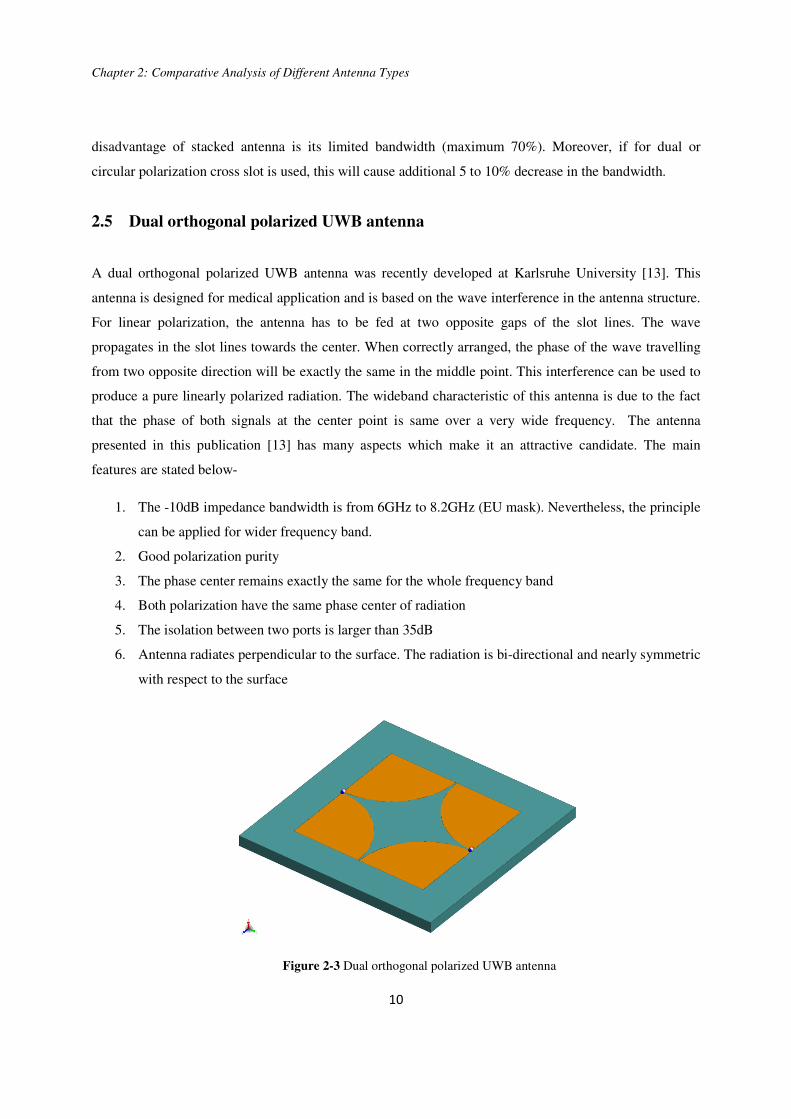
2.5 Dual orthogonal polarized UWB antenna
A dual orthogonal polarized UWB antenna was recently developed at Karlsruhe University [13]. This
antenna is designed for medical application and is based on the wave interference in the antenna structure.
For linear polarization, the antenna has to be fed at two opposite gaps of the slot lines. The wave
propagates in the slot lines towards the center. When correctly arranged, the phase of the wave travelling
from two opposite direction will be exactly the same in the middle point. This interference can be used to
produce a pure linearly polarized radiation. The wideband characteristic of this antenna is due to the fact
that the phase of both signals at the center point is same over a very wide frequency. The antenna
presented in this publication [13] has many aspects which make it an attractive candidate. The main
features are stated below-
1. The -10dB impedance bandwidth is from 6GHz to 8.2GHz (EU mask). Nevertheless, the principle
can be applied for wider frequency band.
2. Good polarization purity
3. The phase center remains exactly the same for the whole frequency band
4. Both polarization have the same phase center of radiation
5. The isolation between two ports is larger than 35dB
6. Antenna radiates perpendicular to the surface. The radiation is bi-directional and nearly symmetric
with respect to the surface
Figure 2-3 Dual orthogonal polarized UWB antenna
Chapter 2: Comparative Analysis of Different Antenna Types
11
A FEKO model of this proposed antenna structure was constructed to get some initial understanding and
is presented in Figure 2-3. In this FEKO model, the same substrate material was used as in [17] (Duroid
5880 with rε =2.2 and thickness 0.79 mm). Here, the dimension of the antenna is 10x10 mm and wire
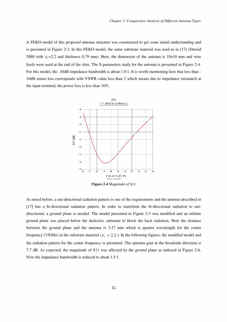
feeds were used at the end of the slots. The S-parameters study for the antenna is presented in Figure 2-4.
For this model, the -10dB impedance bandwidth is about 1.8:1. It is worth mentioning here that less than -
10dB return loss corresponds with VSWR value less than 2 which means due to impedance mismatch at
the input terminal, the power loss is less than 10%.
Figure 2-4 Magnitude of S11
As noted before, a uni-directional radiation pattern is one of the requirements and the antenna described in
[17] has a bi-directional radiation pattern. In order to transform the bi-directional radiation to uni-
directional, a ground plane is needed. The model presented in Figure 2-3 was modified and an infinite
ground plane was placed below the dielectric substrate to block the back radiation. Here the distance
between the ground plane and the antenna is 3.37 mm which is quarter wavelength for the center
frequency (15GHz) in the substrate material ( 2.2=rε ). In the following figures, the modified model and
the radiation pattern for the center frequency is presented. The antenna gain at the broadside direction is
7.7 dB. As expected, the magnitude of S11 was affected by the ground plane as indicted in Figure 2-6.
Now the impedance bandwidth is reduced to about 1.5:1.

Chapter 2: Comparative Analysis of Different Antenna Types
12
Figure 2-5 FEKO model of the antenna with ground plane at the center frequency
Figure 2-6 Magnitude of S11 for ground plane at 3.37mm away from the antenna

Chapter 2: Comparative Analysis of Different Antenna Types
13
2.6 Cross bowtie antenna
A dipole antenna created by Heinrich Rudolph Hertz is the simplest practical antenna. The radiation of the
thin wire dipole is caused by the incident field from the feed and the strong diffractions from the edges.
The magnitude and the phase of these fields determine the bandwidth and the radiation characteristics. A
simple dipole antenna has a narrow operational bandwidth. It is well known that thickening the dipole
wire (decreasing the l/d ratio) will increase its bandwidth. It has been documented in [14] that l/d ≈ 5000
provides a bandwidth of about 3% while l/d ≈ 260 has a bandwidth close to 30%.
Over the years many work has been done to transform a simple dipole to a wideband antenna and the
result is the many variations of the dipole, such as bow tie, butterfly and diamond dipole. Bow-tie antenna
is one of the most commonly used variants. Due to their broadband characteristic and simple geometry,
the bow-tie antenna has become an important candidate for UWB applications. It is basically a planar
cross section of the biconical antenna. The broadband characteristic of the bow-tie antenna is caused by
the incoherent diffractions of four corners and two edges. The diffracted fields have different phase at a
specific frequency which causes a wider bandwidth [15]. The realization of a dual orthogonal polarized
bow-tie antenna with common phase center can be obtained by placing two linear polarized elements
orthogonal to each other as presented in Figure 2-7.
Figure 2-7 Dual polarized cross bowtie antenna, left: basic configuration, right: rounded edge configuration
A simulation model of two orthogonal bow-tie antennas for the basic configuration and for the rounded
edge configuration (Figure 2-7) was created. For these simplified models the substrate material was
removed and the antennas were fed by wire ports. In this model the length of each arm is 15 mm, the
width is 8.7 mm and the flare angle is 60°. Simulation result presented in Figure 2-8, indicates that the

Chapter 2: Comparative Analysis of Different Antenna Types
14
input impedance is very high for this structure. Therefore, it becomes very difficult to obtain a good
impedance match for a broad band. In Figure 2-9, the magnitude of S11for the rounded edge bow tie is
presented. Here, the reference impedance was set to 100 Ω and this provides a return loss below -10 dB
only between 12 and 14 GHz.
Figure 2-8 Input impedance of the rounded edge bow-tie
Figure 2-9 Magnitude of S11of the rounded edge bow-tie
This limited bandwidth of the bow-tie antenna is a drawback. Even without a ground plane it is difficult to
receive sufficient bandwidth. Simulation results indicated an increase in this band when the gap between
the two arms is reduced (g in Figure 2-10) or when the width of feed point is increased (w in Figure 2-10).
As in this case two antenna elements are inserted orthogonally, reducing the gap or increasing the feed
width is not a practical solution. It is well known that the bandwidth of a bow tie antenna can be
significantly increased by using resistive loading. However, this will reduce the efficiency.

Chapter 2: Comparative Analysis of Different Antenna Types
15
Figure 2-10 Bowtie antenna element
2.7 Tran antenna
In recent time, a novel X-band antenna for phase array application was developed at Delft University
(IRCTR) by D. P. Tran, et. al [16]. I shall call it as the Tran antenna in the thesis. This antenna possesses
very good UWB characteristics in the designed spectrum (5 to 15 GHz). These include a nearly perfect
linear phase, sub-nanosecond deviations in the group delay and a very wide bandwidth (about 100%
fractional bandwidth). Another favorable aspect of this antenna is its uni-directional radiation pattern
which is one of the major requirements for this project. This antenna is compact, 13x13mm which
corresponds to less than half of the free-space wavelength at the center frequency. Therefore, this antenna
is very suitable to use in an array application. In [16] it has been stated that the antenna is able to provide
constant and high transmission power with in-band deviation of 0.1dB. The X-band transmission
efficiency of this radiator is over 94%.
Figure 2-11 Tran antenna model implemented in CST

Chapter 2: Comparative Analysis of Different Antenna Types
16
The antenna proposed in [16] can be regarded as a quasi electromagnetic antenna. A detail discussion on
the definition of electric and magnetic antenna can be found in [17]. When the magnetic field of a radiator
is orthogonal to the antenna plane over most of the antenna aperture, it can be denoted as the quasi-
magnetic antenna. On the other hand, when the electric field is orthogonal to the antenna plane over most
of the aperture, it is denoted as the quasi-electric antenna. For the antenna presented in this section not
only the magnetic field but also the electric field is normal to the antenna plane due to the presence of the
ground plane underneath the substrate and therefore referred to as a quasi electromagnetic antenna.
As demonstrated in Figure 2-11, the antenna is formed by a path encircled by a ring. Four stubs are
attached to the upper side of the ring. The inner stubs are important for the lower resonance. These stubs
are producing additional path length for the current and the S11 pattern shifts towards the lower frequency
band. The length of the outer stubs is important for the higher resonant frequency. By introducing these
outer stubs, we are reducing the loop area and moving the operational band towards the higher
frequencies. The notch length at the patch has a great influence on balancing the reflection. Both the notch
and the inner stubs are forcing the current to flow to the end of the patch which counteracts with the
resonant behavior.
A major advantage of the Tran antenna is its uni-directional radiation pattern. Most UWB antennas are bi-
directional. A uni-directional radiation pattern is often achieved by placing a ground plane at a certain
distance (usually at quarter wavelength at the center frequency) from the antenna. As mentioned before,
the back plane causes a total reflection of the wave when it is quarter wavelength away from the antenna
plane. For other frequencies the reflection mostly increased which degrades the impedance bandwidth. For
the above antenna structure a ground plane is placed directly under the lower substrate and all the multiple
reflections are totally or partially compensated by the added shape.
A feeding technique has a major effect on the overall antenna performance. The proposed antenna is fed
by a grounded coplanar waveguide (CPWG). Here, the signal and gap width values are chosen such that
characteristic impedance of the line will be 50 Ω. It has been demonstrated in [18] that CPW feed
structure has many advantages for wideband applications. Coplanar waveguide has simple structure,
constant effective permittivity, low radiation and conductance losses and very wide operational
bandwidth. Moreover, coplanar waveguide can be easily integrated with microwave integrated circuit and
surface mount devices. This gives the possibility to avoid expensive through-hole technology and thus
reduce the manufacturing cost. However, in array application this surface feeding arrangement has some
practical disadvantages when strict element spacing is needed.

Chapter 2: Comparative Analysis of Different Antenna Types
17
The simulation model of the antenna structure is presented in Figure 2-11. This model was simulated by
using the commercial simulation tool “CST microwave studio”. Both the CPW-feed and the antenna
sections are constructed on top of a high frequency laminate RT5880 (rε =2.2 and thickness 5.537 mm).
All the dimensions of the antenna resembled the original design in [15]. The performance of this antenna
also corresponded very well with the published results. Here, the two most important UWB characteristics
are demonstrated, the return loss and the group delay. In Figure 2-12, we can deduce the presence of two
resonances in the S11 curve which resembles very well the results published in [16]. The phase
characteristic of the simulated antenna is almost linear and hence the group delay is almost constant as
shown in Figure 2-13. This assures that the antenna can be used for UWB imaging.
Figure 2-12 Magnitude of S11 of Tran antenna
Figure 2-13 S11 group delay of Tran antenna

Chapter 2: Comparative Analysis of Different Antenna Types
18
2.8 Comparison of antennas
To provide a clear overview of advantages and disadvantages of different antennas discussed above, a
summary of the comparative analysis of the candidate antennas is presented in table 1. The spiral antenna
is a good candidate as a circular polarized UWB antenna. The major disadvantage is its dispersive
behavior and its bi-directional radiation pattern. Helix on the other hand gives uni-directional pattern but
its non-planar geometry makes it less attractive for our application.
Aperture stacked antenna and cross bowtie antenna have geometrical advantages due to their planar
structures but the disadvantage is their limited bandwidth. Dual orthogonal polarized UWB antenna has
the advantage of wide impedance bandwidth and planar structure. However, it also provides a bi-
directional radiation pattern. Finally the Tran antenna meets most of the design requirements. The only
drawback of this antenna is the linear polarization. Therefore, if it is feasible to generate circular or dual
polarized fields with this antenna structure, we will be able to design an antenna which has a very wide
bandwidth, uni-directional pattern and nearly perfect linear phase.
Table 1 Applicable degrees of antennas (“+++” stands for excellent, “---” stands for unacceptable and the other are
different degree in between)
EM
Characteristics
Planar
Spiral
antenna
Helical
antenna
DOP
UWBA
SMSA Cross
Bowtie
antenna
Tran
antenna
Impedance BW + + + + + + + - + + +
Circular or Dual
Polarized + + + + + + + + + +++ + ++ - - -
Dispersion free - - - - - - + + - - + + +
Uni-directional - - - + + + - - - + + + - - - + + +
Gain + + + + + + + + + + + + + + + + +
Size + + - - - + + + + + + + + +
Chapter 2: Comparative Analysis of Different Antenna Types
19
2.9 Conclusions
In this chapter a comparative analysis of a number of UWB antennas has been performed. In order to get
sufficient data over the antennas, simulation models for a number of them was developed and their
simulations was performed. From these simulations it can be concluded that the Tran antenna shows most
potentials. Thus, it is chosen as the final candidate antenna due to its many advantages over the other
antennas. Nevertheless, this antenna has to be modified for circular or dual linear polarization. For circular
polarization, the amount of data is less compared to dual polarization and hence the data processing will
be faster. However, the advantage of dual orthogonal polarization over circular polarization is that it
provides the full scattering matrix of the target and from two orthogonal polarized fields it is possible in
post-processing to synthesize the circularly polarized field. Therefore, for this project a dual polarized
antenna is more suitable than a circularly polarized antenna. In the next step of my research I am going to
investigate on sub-array which consists of a number of linearly polarized UWB antenna elements and can
be used for creating dual-polarized antennas.

Chapter 3: Dual Orthogonal Polarization with an Array Structure
20
Chapter 3
3 Dual Orthogonal Polarization with an
Array Structure
3.1 Introduction
In the previous chapter a detailed overview of UWB antennas which can provide circular or dual linear
polarization was presented. Advantages and disadvantages of these antennas were compared and finally it
was found that the Tran antenna meets most design requirements. The only drawback of this antenna is
that it was designed for linear polarization. Next stage of the project was devoted to obtain the dual
orthogonal polarization by using this same antenna design.
3.2 Criteria for the dual polarization
There is an increasing demand of dual orthogonally polarization for many applications to provide
polarization diversity. Therefore, dual polarized antennas have received an extensive research interest.
Designing dual polarized antenna has many challenges. Obtaining high isolations and low cross polarized
levels could be considered as the most important ones. The task becomes more difficult when a wide
bandwidth has to be realized in addition.
The isolation between two input ports corresponding with two orthogonal polarizations is a very important
figure of merit for the dual polarization. The isolation can be defined as a ratio of power leaving one port
to the power entering the other port and ideally should be 0 or -∞ dB. Degradation in isolation can be

Chapter 3: Dual Orthogonal Polarization with an Array Structure
21
caused by energy leakage in the feeding network or intra-element coupling. In practical cases isolation
below -20dB is considered as good isolation.
Polarization purity of an antenna is an important aspect and this can be defined as the ability of an antenna
to radiate in one desired polarization. An alternative definition can be the ratio of directivity of two
orthogonal polarizations. Good polarization purity provides high polarization efficiency. For a linearly
polarized antenna it is desired to radiate all the energy in one particular polarization (co-pol component).
In practice always some portion of the energy will be radiated in different polarization and will decrease
the polarization efficiency.
The polarization is described by the locus of the endpoint of the electric field on the axis of propagation as
time progresses. In theory, the reference polarization is the intended polarization while the cross
polarization is the polarization orthogonal to the reference polarization. However, in practice the definition
of reference polarization and cross polarization is not straightforward. Different ways of measuring the
antenna pattern or different coordinate gives different definitions of polarization. An antenna electric field
can be de-composed in different ways. A commonly used de-composition is based on the spherical
coordinate system which is used for describing the far field pattern. In spherical coordinate systems the
bases are the two unit vectors (θ,Φ) tangent to the sphere surface. Another commonly used definition of
cross-polarization can be achieved from the so called Ludwig3 de-composition [19]. In this definition, co
and cross-polarization are related to antenna measurement and is widely used in anechoic chamber
measurements [20]. If we know the magnitude and phase of a spherical coordinate system, the
components in the Ludwig3 are expressed as-
φφ φθ cossin EEEa +=
φφ φθ sincos EEEb −=
Here, one component (either aE or bE ) is the desired co-pol component while the other is the cross-pol
component. For dual orthogonally polarized antenna it is crucial to have low cross-polarization level. High
cross-polarization level will not give the correct polarimetric information of the target and will provide a
corrupted image.

Chapter 3: Dual Orthogonal Polarization with an Array Structure
22
3.3 Two approaches for dual orthogonal polarization generation
There are basically two fundamental approaches to realize the dual orthogonal polarization-
1. Dual polarized antenna elements are used to realize the dual polarization
2. Linear polarized antenna elements are arranged in a group such a way that together they provide
dual polarization
In the first approach, the dual polarization is obtained from a single antenna element which is able to
radiate field in both polarization. For this approach two phase center associated to the two orthogonal
polarizations coincide. An example of this group can be a single patch antenna radiating in both
polarization. Another example is the cross dipole antenna which can be seen as a single dual polarized
element. Here, two linear polarized antenna elements are 90° rotated and orthogonally inserted inside
each other. A demonstration of this approach for bow tie antenna was presented in chapter 2.6 where the
radiating arms of two bow tie dipoles are orthogonally inserted to assemble the cross bow tie antenna.
In the second approach, linearly polarized antenna are grouped together and fed in such a way that they
can radiate fields in two orthogonal planes. For this approach the antenna elements have to be carefully
arranged in order to radiate symmetric patterns in both planes. Moreover, all the elements must be fed
with equal amplitude and with a correct phase to ensure the symmetry of both polarizations. A weakly
excited element will degrade the performance severely.
There are some design challenges associated with the first approach where a single dual polarized antenna
element is used. For example, it is extremely difficult to maintain a reasonably low isolation between two
orthogonal ports when a single element is used for the dual orthogonal polarization. For this project we
would like to use the Tran antenna and modify this element in such a way that it can provide dual
polarizations.
A simulation model of a dual-fed Tran antenna element was designed to explore the possibilities to use the
first approach explained above. The antenna model is illustrated in Figure 3-1. This model posses a
geometrical equality when viewed from the horizontal port or from the vertical port. The major
disadvantage of this model is the extremely high coupling between the ports. In the surface current
distribution it is observed that most current from one port is coupled to the other port. Even placing a
diagonal slot to separate the ports did not provide much improvement.

Chapter 3: Dual Orthogonal Polarization with an Array Structure
23
Figure 3-1 Dual feed Tran antenna, Left: Antenna model, Right: Surface current distribution
To solve the poor isolation of the antenna model demonstrated above, an alternative feeding technique is
needed. For example, the proximity-coupled feed or the aperture-coupled feed can be used. This might
increase the isolation between two ports. However, these feeding techniques do not provide as wide band
as the CPW feed. Moreover, they are difficult to fabricate as two substrate layers are required.
An alternative approach for obtaining the dual orthogonal polarization is to use the linearly polarized
antenna elements in a sub-array structure. This solution will increase the total size but will ensure better
isolation and wider bandwidth. As wide bandwidth is the prime goal of this project, the second approach
provides a better solution.
3.4 Dual polarization with linearly polarized elements
An array structure can provide circular or dual polarization even though when the elements are linearly
polarized. A sub-array of two orthogonal linearly polarized elements can be used to create dual or circular
polarization (Figure 3-2). The angular orientation between the elements is introduced to produce the
orthogonal fields. For dual polarization the elements are fed with equal phase while for circular
polarization they are fed with 90° phase difference. The disadvantage of this configuration is that the
phase centers correspond to two polarizations do not overlap and the 0° or 90° phase relation of the
elements are effected for the off broadside direction. The phase difference of the elements is disturbed by
the spatial phase delay at an angle (θ) greater than 5°.

Chapter 3: Dual Orthogonal Polarization with an Array Structure
24
Figure 3-2 (a) Two-element array, (b) Spatial phase delay
This limitation of the two element array can be solved by a four element (2x2) array. The elements of this
array are arranged in such a way that both polarizations have the same phase centre. Alternatively to this,
in 1986 John Huang presented a technique to use linearly polarized element to generate circular
polarization [21]. This array is now known as the Huang array. A conventional and a Huang array created
with microstrip antennas is presented in Figure 3-3. For both configurations the phase centers of each
polarization lie on the origin of the coordinate system (0,0).
Figure 3-3 2x2 microstrip antenna array (a) Conventional array (b) Huang array
In this 2x2 array structures, we overcome the problem of spatial phase delay of the two elements array.
For the Huang array the spatial phase delay of one row or column is in the opposite sense of the other row
or column and therefore will cancel each other. The only exception is in the diagonal plane. For the
Chapter 3: Dual Orthogonal Polarization with an Array Structure
25
diagonal plane, the far field can be considered as composed of three elements where the amplitude of the
center element is two and the amplitude of the end elements is one. Therefore, there will phase and
polarization imbalances in the diagonal plane and cross-pol level will be high.
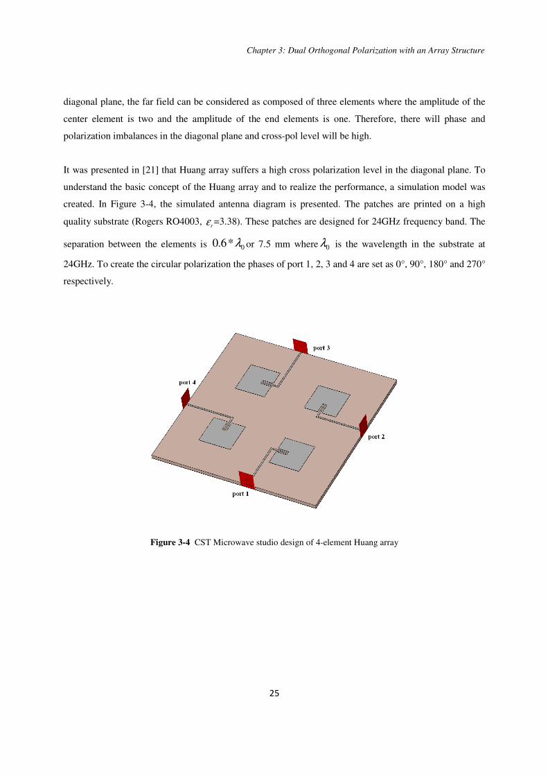
It was presented in [21] that Huang array suffers a high cross polarization level in the diagonal plane. To
understand the basic concept of the Huang array and to realize the performance, a simulation model was
created. In Figure 3-4, the simulated antenna diagram is presented. The patches are printed on a high
quality substrate (Rogers RO4003, rε =3.38). These patches are designed for 24GHz frequency band. The
separation between the elements is 0*6.0 λ or 7.5 mm where 0λ is the wavelength in the substrate at
24GHz. To create the circular polarization the phases of port 1, 2, 3 and 4 are set as 0°, 90°, 180° and 270°
respectively.
Figure 3-4 CST Microwave studio design of 4-element Huang array

Chapter 3: Dual Orthogonal Polarization with an Array Structure
26
Figure 3-5 Axial ratio of the four element array in the principle plane
In the above figure, the axial ratio of the Huang array is plotted. Here we see that the axial ratio of the
circularly polarized wave is indeed less than 3 dB for theta angle less than 40°. This simulation result
verifies that the Huang array overcomes the shortcoming of the spatial phase delay problem of the two
element array and can maintain the necessary phase relation between two orthogonally polarized fields for
a large angle. This gives the possibility to scan the main beam of the antenna in the principle plane to a
large angle from the broadside direction.
The circular polarization is composed of two orthogonal and independent components- Left hand circular
and right hand circular. The desired sense of rotation (in this simulation LHCP) is the co-polarized
component and the undesired component (here RHCP) is the cross polarized component. Figure 3-6
illustrates the co-polarized (LHCP) and the cross-polarized (RHCP) part of the farfield. In the principle
plane the cross-pol component is very low. At the broadside direction the cross-pol is 40 dB lower than
the co-pol. However, high cross polarized lobes exist in the diagonal planes. Especially when we move
from the broadside direction in the diagonal plane, the cross polarized field becomes high. Nevertheless,
for this model the cross-pol level is still lower than the co-pol level for an angle less than 33°.
Furthermore, this phenomenon can be solved in a large array by averaging the imbalances. Therefore, this
Huang array structure is considered as an attractive solution for this project. So, in this project two

Chapter 3: Dual Orthogonal Polarization with an Array Structure
27
different types of sub-array arrangement will be investigated: the conventional array where the
polarization planes lies on the two principle planes and the Huang array.
Figure 3-6 Co and cross polarized far-field radiation pattern of the Huang array
Figure 3-7 Co and Cross polarized field for phi=45° plane

Chapter 3: Dual Orthogonal Polarization with an Array Structure
28
3.5 Conclusions
In this chapter the fundamental concept of generation of the dual orthogonal polarization was presented.
Two different approaches were discussed. The first approach uses a single dual polarized element, while
the second approach uses several linear polarized antenna elements in an array. It was pointed out that the
second approach will provide a better solution. The poor isolation between two ports made the first
approach unsuitable for this project. In the later stage of this project an array structure of the Tran antenna
was used for the dual polarization.
Furthermore, in this chapter we presented two possible solutions for the array structure: the conventional
array and the Huang array. The advantage of the Huang array is the possibility to bring the antenna
elements closer than in a conventional arrangement. This will reduce the total size of the array. Another
major advantage of the Huang array is the relatively low mutual coupling due to the relative orientation of
the adjacent elements. For the conventional array structure, the element spacing is higher and it is known
that when the separation between elements is increased, more power will be transferred from the main
lobe to the side lobe which will decrease the beam-width and side lobes will appear. On the other hand,
the conventional array provides a simple configuration and good polarization purity. Therefore, in this
project both the conventional array and the Huang array was used to create the wideband dual polarized
sub-array. The design procedure and the outcomes are presented in chapter 6.

Chapter 4: Antenna Element for 8 to 24 GHz Frequency Band
29
Chapter 4
4 Antenna Element for 8 to 24 GHz
Frequency Band
4.1 Introduction
In chapter 2, the Tran antenna was introduced. Due to its many promising features it has been chosen as
the most interesting antenna structure for this project. This antenna structure can be used inside an antenna
array to create the desired dual orthogonal polarization. The Tran antenna was designed for the X-band
phased array applications. For many other applications, such as the concealed weapon detection, the Ku-
band is of great interest. In this chapter, the antenna element will be re-designed to shift the operational
bandwidth towards the higher frequency band.
It is well known that the operating frequency band of an antenna structure can be shifted towards a lower
frequency band by enlarging its geometrical dimensions. On the other hand, the operating frequency band
can be shifted towards a higher frequency band by shrinking its geometrical dimensions. In many
practical situations, scaling all the parameters of an antenna by a same scaling factor cannot ensure the
optimum solution and the performance might decrease drastically. Therefore, a careful analysis of
different parameters is required. In this chapter, the scaling factor will be illustrated followed by the
parametric study of a new antenna. After that, the performance of the new antenna will be studied in
details. In the following numerical methods will be used for analysis and optimization of antenna
structure. Here CST microwave studio was used as the EM solver as it can provide good accuracy with
low computation cost (time and memory). Detail discussion on the choice of the EM solver is presented in
Appendix B.
Chapter 4: Antenna Element for 8 to 24 GHz Frequency Band
30
4.2 Scale factor
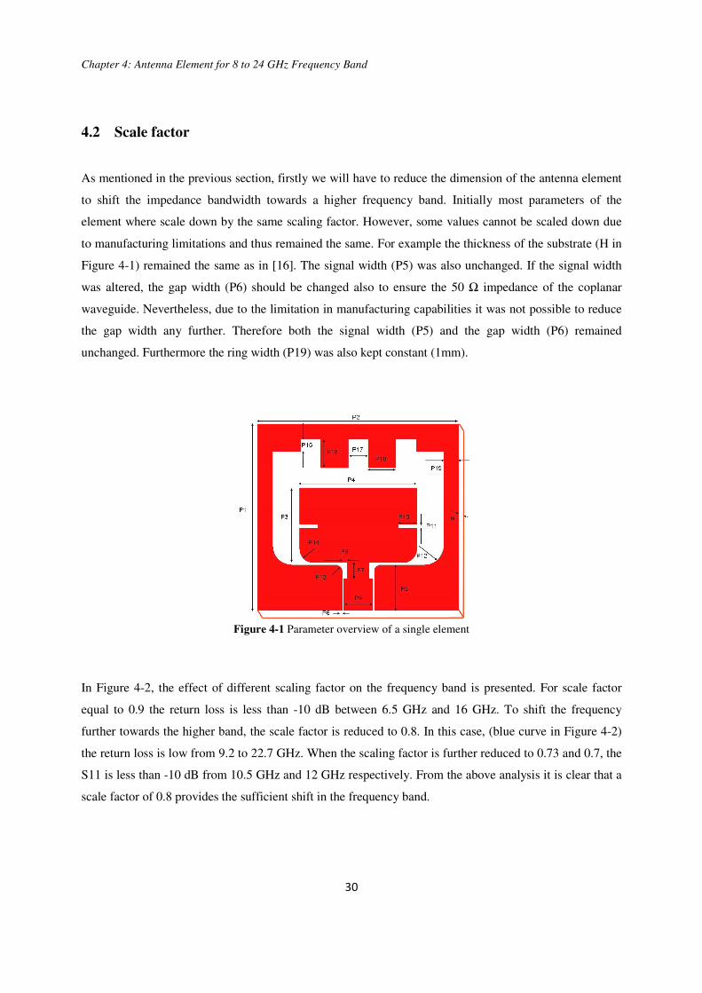
As mentioned in the previous section, firstly we will have to reduce the dimension of the antenna element
to shift the impedance bandwidth towards a higher frequency band. Initially most parameters of the
element where scale down by the same scaling factor. However, some values cannot be scaled down due
to manufacturing limitations and thus remained the same. For example the thickness of the substrate (H in
Figure 4-1) remained the same as in [16]. The signal width (P5) was also unchanged. If the signal width
was altered, the gap width (P6) should be changed also to ensure the 50 Ω impedance of the coplanar
waveguide. Nevertheless, due to the limitation in manufacturing capabilities it was not possible to reduce
the gap width any further. Therefore both the signal width (P5) and the gap width (P6) remained
unchanged. Furthermore the ring width (P19) was also kept constant (1mm).
Figure 4-1 Parameter overview of a single element
In Figure 4-2, the effect of different scaling factor on the frequency band is presented. For scale factor
equal to 0.9 the return loss is less than -10 dB between 6.5 GHz and 16 GHz. To shift the frequency
further towards the higher band, the scale factor is reduced to 0.8. In this case, (blue curve in Figure 4-2)
the return loss is low from 9.2 to 22.7 GHz. When the scaling factor is further reduced to 0.73 and 0.7, the
S11 is less than -10 dB from 10.5 GHz and 12 GHz respectively. From the above analysis it is clear that a
scale factor of 0.8 provides the sufficient shift in the frequency band.

Chapter 4: Antenna Element for 8 to 24 GHz Frequency Band
31
Figure 4-2 Frequency band for different scaling factor
4.3 Parametric study
From the previous investigation it is clear that to design an antenna element for the Ku-band, 0.8 is the
optimum value for the scaling factor. However, simulation result shows that the return loss is not
sufficiently low (< -10dB) within the entire operating band. Therefore, some important parameters of the
element need to be optimized to reduce the return loss.
A parametric study has been conducted to evaluate the influence of different parameters of the antenna
element. For this study the “parameter Sweep” of CST was used as using “Optimizer” is not a practical
solution due to the large number of parameters. In the following section, the parametric study of five
significant parameters are presented which is the patch length (P3), patch width (p4), the curve radius
(P13), the impedance transformer width (P9) and the outer stub length (P15).
Firstly, the patch length was varied from 3 to 4.25 mm. In Figure 4-3, we can see that the patch length has
a great influence on the lower frequency band. After scaling the patch length was 3.96 mm (orange curve
in Figure 4-3). When the length was increased to 4.25 mm, the return loss increased for the lower
frequency band. On the other hand when the length was decreased, the antenna shows clear resonance
around 10GHz which makes the structure dispersive. P3=3.5 mm provides a good balance between return
loss and group delay.

Chapter 4: Antenna Element for 8 to 24 GHz Frequency Band
32
Secondly, the effect of the patch width was investigated (Figure 4-4). The patch width has a clear
balancing effect between the lower and higher frequency bands. On the other hand, the curve radius P13
(Figure 4-5) has a balancing effect between the lower, centre and higher frequency bands. P4=6.25 mm
and P13=0.8 mm provides a good balance.
Next, the impedance transformer width was changed. The purpose of the impedance transformer is to
provide a good matching between the 50 Ω coax cable and the antenna input impedance over a large
frequency band. Figure 4-6 shows that the transformer width has most effect on the centre frequency. The
return loss at the centre frequency is minimized when the transformer width is increased or p9 is
decreased. Therefore, P9 was set to zero in the final design. In Figure 4-7, the outer stub length’s effect is
illustrated. This parameter is more important for the centre and higher frequencies.
Figure 4-3 The patch length’s effect
Figure 4-4 The patch width’s effect

Chapter 4: Antenna Element for 8 to 24 GHz Frequency Band
33
Figure 4-5 The curve radius’s effect
Figure 4-6 Transformer width’s effect
Figure 4-7 The outer stub length’s effect
Chapter 4: Antenna Element for 8 to 24 GHz Frequency Band
34
4.4 Analysis of the 8 to 24GHz antenna element
In the previous section the parametric study for the Ku-band antenna elements is presented. After carefully
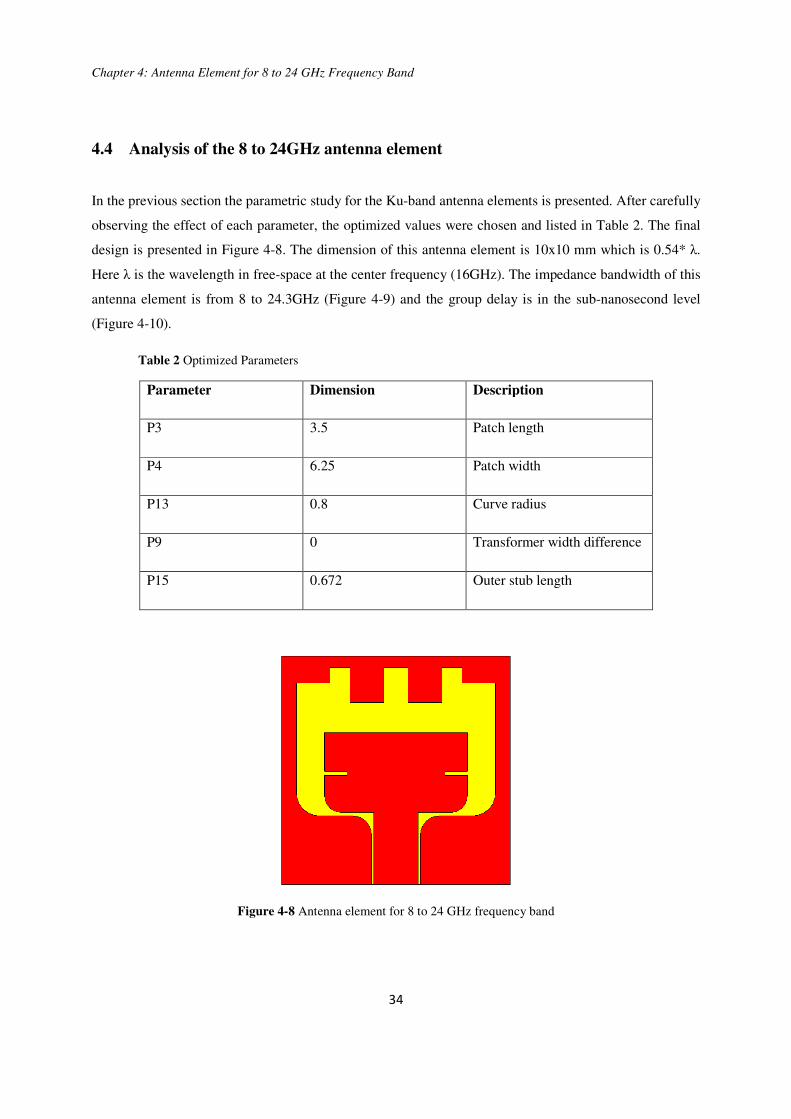
observing the effect of each parameter, the optimized values were chosen and listed in Table 2. The final
design is presented in Figure 4-8. The dimension of this antenna element is 10x10 mm which is 0.54* λ.
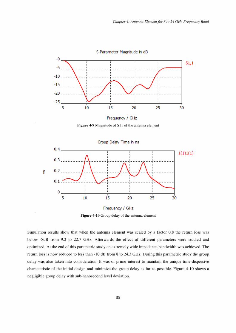
Here λ is the wavelength in free-space at the center frequency (16GHz). The impedance bandwidth of this
antenna element is from 8 to 24.3GHz (Figure 4-9) and the group delay is in the sub-nanosecond level
(Figure 4-10).
Table 2 Optimized Parameters
Parameter Dimension Description
P3 3.5 Patch length
P4 6.25 Patch width
P13 0.8 Curve radius
P9 0 Transformer width difference
P15 0.672 Outer stub length
Figure 4-8 Antenna element for 8 to 24 GHz frequency band
Chapter 4: Antenna Element for 8 to 24 GHz Frequency Band
35
Figure 4-9 Magnitude of S11 of the antenna element
Figure 4-10 Group delay of the antenna element
Simulation results show that when the antenna element was scaled by a factor 0.8 the return loss was
below -8dB from 9.2 to 22.7 GHz. Afterwards the effect of different parameters were studied and
optimized. At the end of this parametric study an extremely wide impedance bandwidth was achieved. The
return loss is now reduced to less than -10 dB from 8 to 24.3 GHz. During this parametric study the group
delay was also taken into consideration. It was of prime interest to maintain the unique time-dispersive
characteristic of the initial design and minimize the group delay as far as possible. Figure 4-10 shows a
negligible group delay with sub-nanosecond level deviation.

Chapter 4: Antenna Element for 8 to 24 GHz Frequency Band
36
Figure 4-11 Radiation pattern of the array structure in H-plane for different frequencies
Besides the reflection coefficient and the time-dispersive behavior, the radiation characteristic is also very
important. In Figure 4-11, the radiation pattern of the antenna element for different frequencies is plotted.
Here we notice that the beam is pointing in the same direction over an extremely wideband. The pattern
also does not contain any side loop up to 22 GHz. The back radiation is high for the lower band, for
example at 10 GHz the front-to-back ratio (FBR) is 2.2 dB. The FBR gradually increases with frequency.
At 16 GHz and 18GHz the FBR is 10.8 dB and 13 dB respectively. The antenna element also possesses a
wide beam width. The half power beam width at 16GHz is 104°. In Figure 4-12, the co-polarized and the
cross-polarized field at the center frequency (16 GHz) is presented. While the polarization is extremely
pure in the E plane (phi=90°), a significant amount of cross polarization level is observed in the H plane
(phi=0°). For determining the co and cross polarized field the Ludwig 3 coordination system was used.
Figure 4-12 Fairfield radiation pattern at the center frequency (16GHz) of the Ku-band antenna element, Left: co-
polarized field. Right: cross-polarized field

Chapter 4: Antenna Element for 8 to 24 GHz Frequency Band
37
In Figure 4-12 the co and cross polarized fields are illustrated. From this figure we know that the cross-pol
level is minimum in the E-plane (phi=90°) and maximum in the H-plane (phi=0°). In the following figure
co and cross-pol fields for different frequencies in H-plane is presented. Cross-pol level is extremely low
in the broad side direction over the entire band. For theta angle greater than 30° the cross-pol level
increases with frequency.
Figure 4-13 Co and cross polarized fields in H-plane (phi=0°) at different frequencies as a function of theta angle

Chapter 4: Antenna Element for 8 to 24 GHz Frequency Band
38
4.5 Conclusions
In this chapter, I have designed the Ku-band Tran antenna. As a first step in this design, the geometrical
dimensions of the X-band antenna were scaled down. This provided the necessary shift in the impedance
band but fail to provide a low return loss over the entire bandwidth of interest. After that a parametric
study was performed. During this study the most important geometric parameters were investigated and
their effects on the antenna input impedance were very carefully monitored. For each parameter an
optimum value was chosen. An antenna model containing these optimum values was designed. Finally,
the performance of this antenna has been studied. The antenna model satisfies the requirements in terms of
impedance bandwidth (3:1), size (half of the free-space wavelength at the center frequency), time-
dispersive characteristic and radiation pattern.

Chapter 5: Wideband Perpendicular Coax-to-coplanar Transition
39
Chapter 5
5 Wideband Perpendicular Coax-to-
coplanar Transition
5.1 Introduction
In the previous chapters the antenna element and the array configurations are discussed. In practice
besides designing the antenna geometry, feeding these antennas is also a challenge and a competitive
research area. The antenna elements designed during this project are fed by coplanar waveguide.
However, in this way antennas cannot be connected to the measurement system. The measurement of
these antennas can only be performed with a coaxial measurement system. Therefore, there is an
unavoidable need of coaxial-to-coplanar transition which can assure minimum transmission loss for a
wideband. Traditionally surface feeding arrangement is used for the transition of coaxial to coplanar
where the axis of the coaxial connector is aligned with the end of the coplanar line. The inner connector of
the coaxial cable is connected with the centre signal line of the coplanar waveguide and the outer
connector with the coplanar ground plates as shown Figure 5-1 (a). This end-launch geometry has some
practical disadvantages. The major disadvantage for this project is the addition space required for the
connector which will increase the total surface area required for each element. This might become a
challenge when in future state the antenna elements should be placed inside an array structure especially
when strict element spacing has to be maintained. Therefore, during this thesis project attention has been
paid to design a perpendicular transition of coaxial to coplanar transmission line.
In Figure 5-1 (b), an example of a right-angle coax-to-coplanar transition is illustrated. Here the radial
electric field of the coax directly couples on the same plane with the electric field in the gap between the
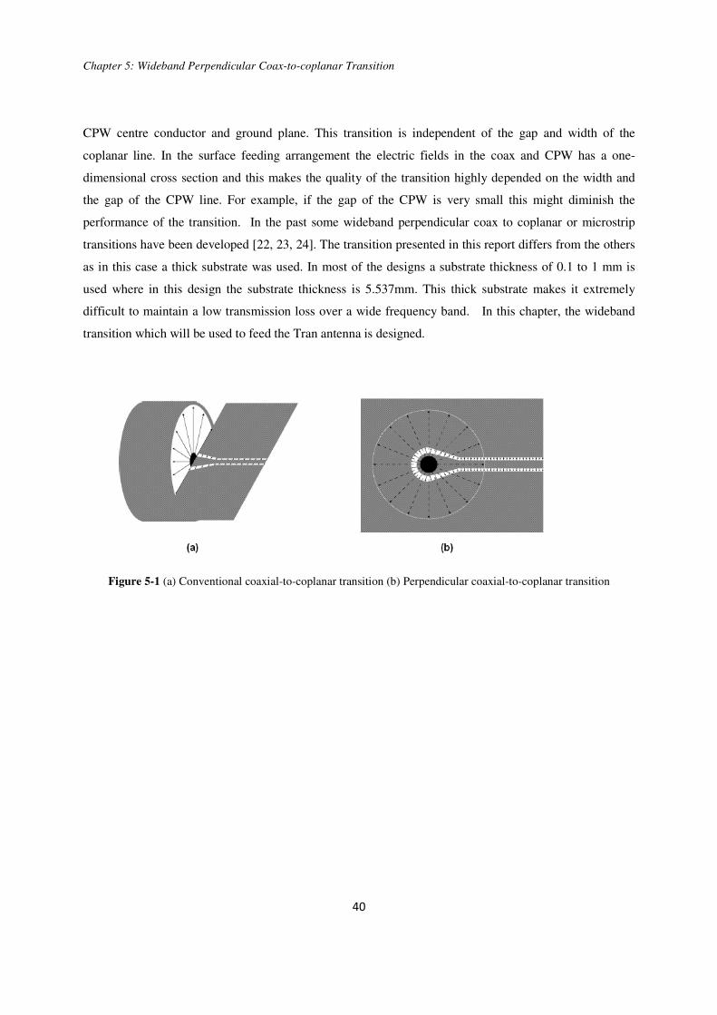
Chapter 5: Wideband Perpendicular Coax-to-coplanar Transition
40
CPW centre conductor and ground plane. This transition is independent of the gap and width of the
coplanar line. In the surface feeding arrangement the electric fields in the coax and CPW has a one-
dimensional cross section and this makes the quality of the transition highly depended on the width and
the gap of the CPW line. For example, if the gap of the CPW is very small this might diminish the
performance of the transition. In the past some wideband perpendicular coax to coplanar or microstrip
transitions have been developed [22, 23, 24]. The transition presented in this report differs from the others
as in this case a thick substrate was used. In most of the designs a substrate thickness of 0.1 to 1 mm is
used where in this design the substrate thickness is 5.537mm. This thick substrate makes it extremely
difficult to maintain a low transmission loss over a wide frequency band. In this chapter, the wideband
transition which will be used to feed the Tran antenna is designed.
Figure 5-1 (a) Conventional coaxial-to-coplanar transition (b) Perpendicular coaxial-to-coplanar transition
Chapter 5: Wideband Perpendicular Coax-to-coplanar Transition
41
5.2 The perpendicular transition design
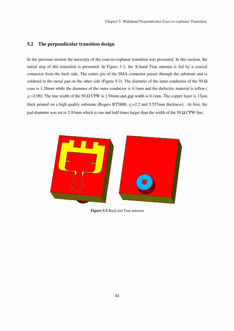
In the previous section the necessity of the coax-to-coplanar transition was presented. In this section, the
initial step of this transition is presented. In Figure 5-2, the X-band Tran antenna is fed by a coaxial
connector from the back side. The centre pin of the SMA connector passes through the substrate and is
soldered to the metal pad on the other side (Figure 5-3). The diameter of the inner conductor of the 50 Ω
coax is 1.28mm while the diameter of the outer conductor is 4.1mm and the dielectric material is teflon (
rε =2.08). The line width of the 50 Ω CPW is 1.94mm and gap width is 0.1mm. The copper layer is 17µm
thick printed on a high quality substrate (Rogers RT5880, rε =2.2 and 5.537mm thickness). At first, the
pad diameter was set to 2.91mm which is one and half times larger than the width of the 50 Ω CPW line.
Figure 5-2 Back-fed Tran antenna

Chapter 5: Wideband Perpendicular Coax-to-coplanar Transition
42
Figure 5-3 Transparent view of the coax-to-coplanar transition, (a) front view (b) side view
Figure 5-4 S-parameter for the design presented in Figure 5-2
In the above figure the reflection coefficient of the antenna element fed by the orthogonal transition is
presented. The transition presented above is the preliminary model and from the S11 diagram (Figure 5-4)
it is clear that only for a very limited bandwidth the transmission loss is low enough.

Chapter 5: Wideband Perpendicular Coax-to-coplanar Transition
43
5.3 The truncated crown of vias
In the previous transition the top and the bottom ground planes are not connected. Simulation results
showed that only connecting the top and the bottom ground planes with one or two vias is not sufficient.
Instead a truncated crown of vias provides a much better transition (Figure 5-5). This prevents the
undesired propagation in the substrate [25, 26]. From the return loss graph (Figure 5-6) we can see that
here multiple resonance are present. Simulation results shows that an optimum value for the diameter of
the truncated vias is 0.5mm. Reducing the diameter value will increase the manufacturing cost while
increasing this value will degrade the performance.
Figure 5-5 Coax-to-coplanar transition with truncated crown of vias
Figure 5-6 Return loss of the transition presented in Figure 5-5

Chapter 5: Wideband Perpendicular Coax-to-coplanar Transition
44
The truncated crown of vias introduced in the previous design behaves like a coaxial line where the vias
create the outer conductor. In that case we will get the best match when the impedance of this coax line is
also 50 Ω. Here the dielectric material is Rogers RT5880 and the relative permittivity is 2.2.
Figure 5-7 Coaxial line model
The impedance of coaxial cable, )ln(*2
1
a
bZ
ε
µ
π=
Where,
a = diameter of the inner conductor
b= diameter of the outer conductor
ε = permittivity of the dielectric
µ= permeability of the dielectric
)2exp(*µ
επZab = )
10*4
2.2*10*854.850*2exp(*28.1
7
12
−
−
=π
π mm4.4=
So, the diameter of the outer connector or in this case the distance between the center connector and the
truncated vias should be 4.4mm to bring the impedance close to 50 Ω.

Chapter 5: Wideband Perpendicular Coax-to-coplanar Transition
45
A model of the antenna was created where the distance between the center pin and the truncated vias was
increased to 4.4 mm (Figure 5-8). In this model, 13 vias are used and the distance between two vias is 0.47
mm. This modification provides a better impedance match between the coax and the coplanar line. For
this transition with the 50 Ω truncated crown of vias the real part of the input impedance periodically tends
to go to 50 Ω. Therefore, the mismatch also reduces periodically.
Figure 5-8 The truncated crown of vias are used to make a 50 Ω coax line inside the Rogers material
Figure 5-9 Return loss of the transition presented in Figure 5-8

Chapter 5: Wideband Perpendicular Coax-to-coplanar Transition
46
Figure 5-10 Input impedance of the transition presented in Figure 5-8 (green curve) and input impedance of the
transition presented in Figure 5-2 (red curve)
In the design presented in Figure 5-8 the vias are shifted so that the distance between the center connector
and the truncated vias is 4.4mm but in this design these vias did not circulate the inner conductor
completely. As a coplanar line is connecting the transition pad to the radiating antenna patch, in that
region no vias could be placed. On the other hand, as our substrate material is made of three layers it gives
us the opportunity to place blind vias underneath the coplanar waveguide as illustrated in Figure 5-11 and
Figure 5-12. Blind vias are via holes which are used to connect the outer layer with inner layers, but do
not go through the entire board. This will provide a better prevention against the undesired propagation in
the substrate.
Figure 5-11 Top view of the truncated crown of vias

Chapter 5: Wideband Perpendicular Coax-to-coplanar Transition
47
Figure 5-12 Side view of the vias placed beneath the coplanar waveguide
The thickness of the laminate used in this antenna design is 5.537mm. This thickness is achieved by
combining three layers of laminates which has a thickness 0.787mm, 1.575mm and 3.175mm,
respectively. This multilayer substrate gives us the opportunity to insert vias below the coplanar line. Two
models were simulated, in one design the gap between the end of the via and the coplanar line was 0.787
mm while for the other this was 1.575 mm. In the following graph the return losses of these models are
shown. For a gap distance of 1.575mm, we noticed an improvement especially around 10 GHz.
Figure 5-13 Return loss for different gap between the end of the via and the coplanar line
Chapter 5: Wideband Perpendicular Coax-to-coplanar Transition
48
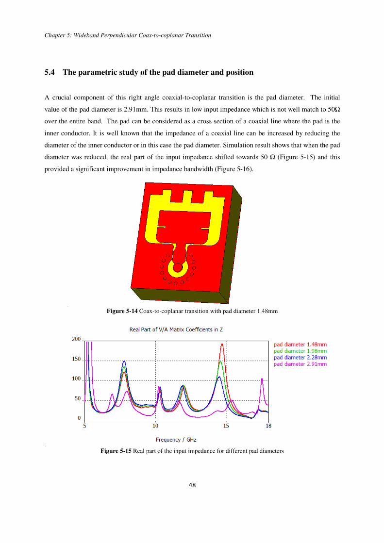
5.4 The parametric study of the pad diameter and position
A crucial component of this right angle coaxial-to-coplanar transition is the pad diameter. The initial
value of the pad diameter is 2.91mm. This results in low input impedance which is not well match to 50Ω
over the entire band. The pad can be considered as a cross section of a coaxial line where the pad is the
inner conductor. It is well known that the impedance of a coaxial line can be increased by reducing the
diameter of the inner conductor or in this case the pad diameter. Simulation result shows that when the pad
diameter was reduced, the real part of the input impedance shifted towards 50 Ω (Figure 5-15) and this
provided a significant improvement in impedance bandwidth (Figure 5-16).
Figure 5-14 Coax-to-coplanar transition with pad diameter 1.48mm
Figure 5-15 Real part of the input impedance for different pad diameters

Chapter 5: Wideband Perpendicular Coax-to-coplanar Transition
49
Figure 5-16 Return loss for different pad diameters
Besides the pad diameter, the feed position is also a critical parameter. It was observed that offsetting the
feed can greatly improve the performance of the transition [24]. This redistributes the parasitic
capacitance, concentrating the fields on that side of the coax line nearest to the outer conductor. It also
reduces the inductance of the signal line by shortening the distance current must flow to get from the
centre pin to the 50 Ω coplanar line.
Figure 5-17 Left: Redistribution of the field by offsetting the pad position, Right: Antenna model where the feed is
0.5 mm shifted towards the coplanar line

Chapter 5: Wideband Perpendicular Coax-to-coplanar Transition
50
From the following graphs it can be observed that the feed position has an impact on the transition
performance. Especially for the lower frequency band (between 7 and 10 GHz), the real part of the input
impedance is close to 50 Ω when the feed is 0.5 mm shifted. By offsetting this feed position we are also
able to diminish the capacitive or inductive reactance. Figure 5-20 shows that for x=0.5 mm the return loss
is less than -10 dB from 7 to 10.5 GHz and less than -6 dB from 6.5 to 14.5 GHz.
Figure 5-18 Real and imaginary part of the input impedance for different offsets (x) of the feed towards the
coplanar line

Chapter 5: Wideband Perpendicular Coax-to-coplanar Transition
51
Figure 5-19 Return loss for different feed position
Figure 5-20 Return loss for feed 0.5 mm shifted towards the coplanar line
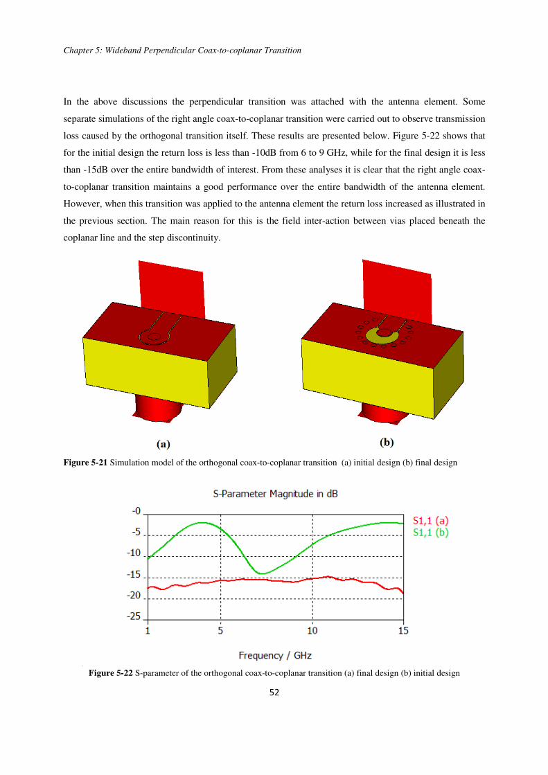
Chapter 5: Wideband Perpendicular Coax-to-coplanar Transition
52
In the above discussions the perpendicular transition was attached with the antenna element. Some
separate simulations of the right angle coax-to-coplanar transition were carried out to observe transmission
loss caused by the orthogonal transition itself. These results are presented below. Figure 5-22 shows that
for the initial design the return loss is less than -10dB from 6 to 9 GHz, while for the final design it is less
than -15dB over the entire bandwidth of interest. From these analyses it is clear that the right angle coax-
to-coplanar transition maintains a good performance over the entire bandwidth of the antenna element.
However, when this transition was applied to the antenna element the return loss increased as illustrated in
the previous section. The main reason for this is the field inter-action between vias placed beneath the
coplanar line and the step discontinuity.
Figure 5-21 Simulation model of the orthogonal coax-to-coplanar transition (a) initial design (b) final design
Figure 5-22 S-parameter of the orthogonal coax-to-coplanar transition (a) final design (b) initial design

Chapter 5: Wideband Perpendicular Coax-to-coplanar Transition
53
5.5 Conclusions
This chapter was devoted to the antenna feeding problem. At first, the reasons to change the conventional
end-launch geometry were pointed out. The simulation model of the orthogonal transition was presented
in this chapter. The performance of this model was enhanced by the truncated crown of vias. To further
improve the performance, a parametric study of the pad diameter and its position were conducted. At the
end of these investigations a coax-to-coplanar waveguide transition was designed which showed
outstanding performance from DC to millimeter wave frequencies. Together with antenna optimization
described in the previous chapter, new antenna feeding results in a novel antenna design.

Chapter 6: The Antenna Array Design
54
Chapter 6
6 The Antenna Array Design
6.1 Introduction
Chapter 3 was devoted to the basic concept of dual polarization. It was concluded that for this project,
using linearly polarized antenna element in a sub-array is probably the best choice to obtain the dual
polarization. In this chapter, the simulated models and results of some sub-array structures will be
presented. Here the Tran antenna will be used as the antenna element which has been introduced in
chapter 2 and further analyzed in chapter 4. As noted before, two types of arrays can be used, the
conventional array and the Huang array. In this chapter, the conventional and the Huang array for the 5 to
15 GHz band will be presented first, followed by the conventional and the Huang array designs for the 8
to 24 GHz frequency band.
Often it is assumed that the magnitude, phase and distribution of currents and fields of an isolated element
will remain the same when placed inside an array. In practice, it might change drastically due to the
mutual coupling between elements. Therefore, neither the wide impedance bandwidth nor the negligible
group delay of an element can be guaranteed in an array structure without addition investigations. Hence
in the following sections, beside the geometrical construction topology of an array, its wideband
performance will remain under careful consideration.

Chapter 6: The Antenna Array Design
55
6.2 The conventional array structure
In chapter 3, the basic concept of the four element (2x2) conventional array topology has been pointed out.
It has been explained how a 2x2 array can overcome the problem of spatial phase delay of the two
elements array. In the following section, the simulated models and results of the conventional array
configuration will be presented. The analysis of the conventional array will start with its initial topology
(Figure 6-1). The performance and the limitation of this structure will be pointed out. One of the most
crucial challenges here is to miniaturize the array. During this process the geometrical structure of the
array will change and this might have positive or negative influence on the performance. In chapter 4, the
influence of different parameters (such as the patch and stub dimensions) of the Tran antenna element was
shown. This knowledge was applied in the miniaturization process to avoid performance degradation.
In the conventional array structure, the size of the model is two to three times larger than that of the single
element. Moreover, due to the array structure we are not able to define any electric or magnetic symmetry.
Therefore, the computation time will expand radically. CST microwave studio can provide accurate
analysis with reasonably low computation time (compared to FEKO). Therefore, was chosen as the EM
solver for the following analysis.
6.2.1 The initial topology of the conventional array
Figure 6-1 Initial structure of the 2x2 conventional sub-array

Chapter 6: The Antenna Array Design
56
In Figure 6-1 the initial structure of the conventional array configuration is shown. This sub-array is
designed for 5 to 15 GHz operation band. Here two horizontally and two vertically oriented antenna
elements are used. At this point, the traditional surface feeding arrangement was applied to simplify the
design as well as to reduce the computational time. The elements of the same polarization are physically
rotated to simplify feeding. Therefore, 180° phase difference between two opposite ports is introduced.
An advantage of having out-of-phase fed array is the low level of cross polarization and less coupling
between the antenna elements. The dimensions of the sub-array in Figure 6-1 are 40 x 40 mm which is
1.34 λ in both directions where λ is the wavelength in free-space at the center frequency (10GHz).
In Figure 6-2 the S-parameters of the sub-array are presented. Here we see that the impedance bandwidth
of the elements increased after placing them in the conventional array structure. As presented in chapter 2,
-10 dB impedance bandwidth of an isolated element is from 6.5 to 14.5 GHz while in the array structure it
is from 5.5 to 15.5 GHz. This deviation is mainly caused by the mutual coupling among the elements.
Besides influencing the impedance matching, the array geometry also caused two additional resonances in
the S11 curve. Furthermore, it can be deduced from Figure 6-2 that the coupling between the elements is
low. On the other hand, the array arrangement has a negative influence on the time-dispersive
characteristic. Figure 6-3 illustrates that the group delay increased from sub nanosecond level (in an
isolated element) to more than 1 ns in the array.
Figure 6-2 S-parameters of the sub-array in Figure 6-1

Chapter 6: The Antenna Array Design
57
Figure 6-3 S11 group delay of the sub-array in Figure 6-1
A three dimensional view of the far-field radiation pattern at 11.5 GHz is presented in Figure 6-4 (11.5
GHz is the center frequency of the simulated 5 to 18 GHz frequency band). The total field for the
horizontal or the vertical polarization is composed of field radiated from two opposite elements. These
two fields are combined in post-processing and illustrated in Figure 6-4. Simulation results indicate a
similar radiation pattern for both polarizations. It can be deduced from Figure 6-4 that the maximum of the
co-polarized pattern is not exactly in the broadside direction. This phenomenon is caused by the large
element spacing in the array structure. The Co-polarization and the cross-polarization are defined by
Ludwig 3 coordinate system [19]. In the principle planes the polarization is extremely pure. However, the
cross polarization is high in the diagonal plane for theta angle greater than 30°. In Figure 6-5, the polar
plot representation of the reference and the cross polarization are shown. It can be inferred from these
graphs that the back radiation is extremely low. The front-to-back ration is about 28 dB at 11.5 GHz.
Furthermore, we notice the presence of side lobes which is also caused by the high element spacing. Here
the sidelobe level is 13 dB lower than the main lobe.

Chapter 6: The Antenna Array Design
58
Figure 6-4 Radiation pattern at 11.5GHz, Left: Co-pol, Right: Cross-pol
Figure 6-5 Polar plot of the co and cross polarization at 11.5GHz, Left: for phi=0° plane, Right: for phi=45° plane

Chapter 6: The Antenna Array Design
59
In the second simulation ground planes of the antenna elements were joined together. In this case, all the
antenna elements share a common ground plane on the top side. This affected the return loss as presented
in Figure 6-7. The impedance bandwidth is now decreased to 3.5 GHz (from 9 to 12.5 GHz). Moreover
the coupling between the elements increased significantly. From this simulation, it is clear that not only
the shape of the radiating patch but also the shape and the size of each ground plane is critical for the
wideband characteristic.
Figure 6-6 Conventional sub-array with joined ground plane
Figure 6-7 S-parameters of the sub-array presented in Figure 6-6

Chapter 6: The Antenna Array Design
60
6.2.2 Miniaturizing the sub-array
The size of the sub-array shown in Figure 6-1 is 40 x 40 mm. As in the future state this sub-array will be
used in a complete array structure, it is our foremost interest to reduce the size of the sub-array as much as
possible without allowing excessive coupling between the elements. In this section the process of
miniaturization of the antenna and its consequences are discussed.
In the first step of the miniaturizing process the top ground plane of the antenna elements are kept separate
which assures less mutual coupling. The corner of each ground plane is mitered and each element is
shifted towards the center of the structure (Figure 6-8). Here the total size of the sub-array is 36 x 36 mm.
In Figure 6-9 the s-parameters of this array structure are presented. Due to the geometrical alteration the
current and field distribution will vary and this causes changes in matching condition. The impedance
bandwidth is now from 5 to 16 GHz and the coupling between two adjacent elements is about -15dB.
However, around 8.5 GHz the S11 curve shows a strong resonance which causes a peak in group delay
Figure 6-8 Sub-array of dimension 36 x 36 mm

Chapter 6: The Antenna Array Design
61
Figure 6-9 S-parameters of the sub-array in Figure 6-8
.
Figure 6-10 Group delay of the sub-array in Figure 6-8
From the preceding analysis it is obvious that changes in the array structure can introduce dispersion in the
signal and the array will become unsuitable for UWB imaging application. Therefore the miniaturizing of
the array has to be done in such a way that no strong resonance in the S11 curve is present.

Chapter 6: The Antenna Array Design
62
In the next step the size of the sub-array was decreased to 32 x 32 mm which is 1.07λ (λ = free-space
wavelength at 10GHz). This sub-array is presented in Figure 6-11. Here the shape of the outer stub was
changed from previous designs and was placed parallel to the gap between two ground planes. The outer
stub length reduces the loop area encircled by each ground plane and by changing this parameter we can
provide a better match as previously demonstrated in Figure 4-7. In the following graphs we can see that
the impedance bandwidth of this sub-array structure is from 5.5 GHz to 14.5 GHz while the coupling did
not increase much from the previous step. The average coupling between two adjacent elements is -15dB
and the total radiation efficiency is about -0.6 dB. Nevertheless, the most important quality of this design
is the very smooth S11 curve which means that the impedance matching is nearly constant over the
operational band.
Figure 6-11 Sub-array of dimension 32 x 32 mm
Figure 6-12 S-parameters of the sub-array in Figure 6-11

Chapter 6: The Antenna Array Design
63
Figure 6-13 Group delay of the sub-array in Figure 6-11
Figure 6-13 verifies the non-resonance behavior of the structure where it is shown that the group delay is
within 0.3 ns. The co and the cross polarized fields for different frequencies are illustrated in Figure 6-14.
The level of cross polarization is extremely low for the principle planes. However, in the diagonal plane
the cross polarization is not negligible. Therefore in Figure 6-14, the polarization purity in the diagonal
plane is demonstrated. Over the entire frequency band the polarization is very pure for the broadside. The
cross polarized component only becomes high for an angle greater than 30°.
For the lower frequency band (for example, at 6 GHz), the cross-pol is low for the front plane. At 6 GHz
the difference between co and cross pol level at θ=30° is about 15 dB. However, for the lower frequency
band the cross-pol level is high for the back radiation and this degrade the front-to-back ratio to about 10
dB. In Figure 6-14, we notice that the cross-pol level increases with frequency for the front radiation while
it decreases for the back radiation. At 11.5 GHz the co-pol and the cross-pol level is equal at θ=30° and
the FBR is increased to 17 dB. Furthermore, it is clear from Figure 6-14 that there is no side lobe for this
array configuration. For the previous configuration, demonstrated in Figure 6-1and Figure 6-8, side lobes
existed. In this case the side lobe vanishes due to the reduction of the elements spacing.

Chapter 6: The Antenna Array Design
64
Figure 6-14 Co and cross polarized fields at different frequencies for phi=45° plane
The sub-array presented in Figure 6-11 has an adequate level of performance. It satisfies most of the
design requirements. However, the size of this array is 32 x 32 mm which is 1.07λ (λ = free-space
wavelength at 10GHz). For some applications where strict element spacing needs to be realized this size
could be still too large. For that reason, it is our goal to design another array configuration where the size
is about one free-space wavelength at 10GHz. To achieve this goal the size of the sub-array is further
reduced to 28 x 28 mm in the following step. This means that the dimension of the array is 0.94λ in each
direction. In this design the shape of the antenna elements is kept as similar as possible to the initial
structure. The corners of the radiating patches are blended to reduce the coupling between two

Chapter 6: The Antenna Array Design
65
neighboring elements. At first the central ground plane was attach to the rest of the ground planes (Figure
6-15 a). Unfortunately for this structure the return loss increased drastically as shown in Figure 6-16(a).
Afterwards, the central ground plane was detached from the rest of the ground planes. In this case the
impedance bandwidth improved compared to the previous step but it is still not sufficient. In both cases,
the coupling increased. The average coupling between two adjacent elements is -18 dB when the ground
plane was attached. For the second design the average coupling increased to about -12 dB. In the second
design the coupling is more due to the absence of the ground plane between two radiating elements.
Figure 6-15 Sub-array of dimension 28 x 28 mm, (a) middle ground plane is attached, (b) middle ground plane is
detached
Figure 6-16 (a) S-parameters of the sub-array shown in Figure 6-15(a), (b) S-parameters of the sub-array shown in
Figure 6-15(b)
The impedance bandwidth of the sub-array structure presented in Figure 6-16 (b) is about 3 GHz.
Simulation results shows that the bandwidth can be improved by blending the sharp corners of the ground
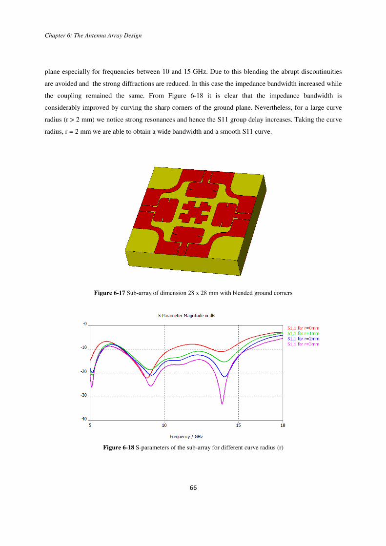
Chapter 6: The Antenna Array Design
66
plane especially for frequencies between 10 and 15 GHz. Due to this blending the abrupt discontinuities
are avoided and the strong diffractions are reduced. In this case the impedance bandwidth increased while
the coupling remained the same. From Figure 6-18 it is clear that the impedance bandwidth is
considerably improved by curving the sharp corners of the ground plane. Nevertheless, for a large curve
radius (r > 2 mm) we notice strong resonances and hence the S11 group delay increases. Taking the curve
radius, r = 2 mm we are able to obtain a wide bandwidth and a smooth S11 curve.
Figure 6-17 Sub-array of dimension 28 x 28 mm with blended ground corners
Figure 6-18 S-parameters of the sub-array for different curve radius (r)

Chapter 6: The Antenna Array Design
67
Figure 6-19 Group delay of the sub-array for different curve radius (r)
Simulation results presented in Figure 6-18 indicates that for r = 2 mm, the return loss is well below -10dB
except between 5 and 8 GHz it becomes more than -10 dB. To reduce this high return loss, a parametric
study of the patch length (p3) and patch width (p4) was conducted. It is found that for p3 = 5.5 mm and p4
= 7 mm, the return loss is less that -10 dB from 4.5 to 15 GHz (Figure 6-21) and the group delay deviation
is less than half nanosecond from 5.5 to 18 GHz (Figure 6-22). In the following figure the CST simulation
model of this array structure is presented.
Figure 6-20 Sub-array for p3=5.5mm and p4=7mm

Chapter 6: The Antenna Array Design
68
Figure 6-21 S-parameters of the sub-array shown in Figure 6-20
Figure 6-22 S11 group delay of the sub-array shown in Figure 6-20
In Figure 6-23, the top view of the three dimensional far-field radiation patterns is shown. As noted
before, the radiation patterns from two opposite elements are combined in post-processing with 180°
phase difference which gives the overall pattern for two orthogonal polarizations. These two patters
resemble each other and they are symmetric around 0°. This implies that both polarizations radiate with
similar performance in all direction. Furthermore, now the maximum of the pattern is exactly in the
broadside direction which was not the case for the first array configuration. This improvement is caused
by the minimized spacing between the elements. However, there is also a drawback of this
miniaturization. The isolation between two patches becomes low. Now some part of the power fed to one

Chapter 6: The Antenna Array Design
69
port will couple to another port. This will reduce radiation efficiency. Furthermore, if the coupling is too
high, this might cause some trouble to the electronic components connected to the antenna. For the
proposed array structure, the coupling is less than -10 dB which means less than 10% of the input power
of a port can enter another port.
Figure 6-23 Fairfield radiation patterns at 10 GHz of the array structure presented in Figure 6-20. Left: antenna
elements along X axis. Right: antenna elements along Y axis
Figure 6-24 Cross polarized field at 10GHz of the array structure presented in Figure 6-20

Chapter 6: The Antenna Array Design
70
Figure 6-25 Co and cross polarized fields for phi=45° plane at different frequencies
In Figure 6-25 the polarization purity of the array is analyzed. Above figure shows that for the broadside
direction the cross polarization level is below -30 dB for the entire impedance bandwidth. However, the
cross polarization is high in the diagonal plane for off broadside. At 8 GHz the difference between the co
and cross polarization is 31 dB for 15° off broadside. As illustrated above the cross polarization level
increases with frequency and at 12 GHz and 14 GHz the difference between the co and cross polarization
for 15° off broadside is 16.7 dB and 6.2 dB respectively. Moreover, above graphs illustrate that for this
configuration a low back radiation is observed over the entire operation band.

Chapter 6: The Antenna Array Design
71
Figure 6-26 Radiation pattern of the array structure for different frequencies
Figure 6-27 Absolute gain (broad-side) versus frequency
The antenna gain is a function of the observation point position over the far field sphere but it is also a
function of frequency. In Figure 6-26 the radiation patterns of the array structure for different frequencies
are presented. Here the radiation pattern is taken for the diagonal plane. In Figure 6-27 the broadside gain
versus the frequency is plotted. For frequency above 6.5 GHz and below 13.5 GHz the gain is positive.
The deviation in the gain is less than 5 dB between 6.5 GHz and 13 GHz.
5 6 7 8 9 10 11 12 13 14 15-6
-4
-2
0
2
4
6
8
Frequency [GHz]
Gain
[d
B]

Chapter 6: The Antenna Array Design
72
Figure 6-28 HPBW versus frequency (E-plane)
In Figure 6-28 the half power beamwidth (HPBW) of the array versus frequency is plotted. Here we notice
wide beamwidth for the lower frequency band. The HPBW decreases to about 70° for 6 to 9 GHz and
decreases further to about 40° for frequency higher than 10 GHz. It can be concluded here that the HPBW
meets the requirement (more than 30°) throughout the band.
To summarize the research described in this section, I can conclude that a polarimetric array with
conventional topology and Tran antennas for the frequency band from 5 to 15 GHz has been designed.
Dimensions of this array are 28mm in both directions. The antenna elements as well as their mutual
positions have been optimized in order to achieve large bandwidth (the impedance bandwidth is more than
10GHz), low coupling between elements (less than -10dB), both reflection and transmission group delay
deviation within sub-nanosecond range, stable radiation pattern, low cross polarization level, sufficient
gain and beamwidth.
5 6 7 8 9 10 11 12 13 14 15
40
60
80
100
120
140
160
Frequency [GHz]
HP
BW
[d
eg
]
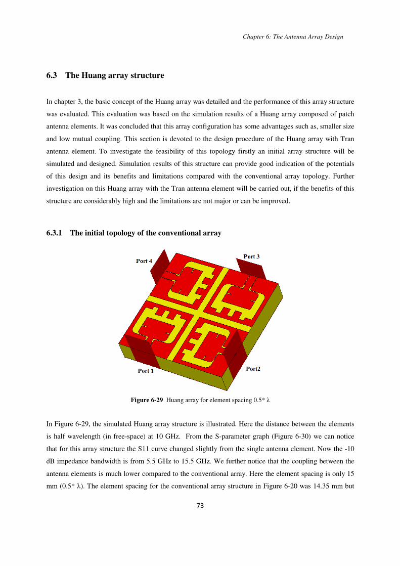
Chapter 6: The Antenna Array Design
73
6.3 The Huang array structure
In chapter 3, the basic concept of the Huang array was detailed and the performance of this array structure
was evaluated. This evaluation was based on the simulation results of a Huang array composed of patch
antenna elements. It was concluded that this array configuration has some advantages such as, smaller size
and low mutual coupling. This section is devoted to the design procedure of the Huang array with Tran
antenna element. To investigate the feasibility of this topology firstly an initial array structure will be
simulated and designed. Simulation results of this structure can provide good indication of the potentials
of this design and its benefits and limitations compared with the conventional array topology. Further
investigation on this Huang array with the Tran antenna element will be carried out, if the benefits of this
structure are considerably high and the limitations are not major or can be improved.
6.3.1 The initial topology of the conventional array
Figure 6-29 Huang array for element spacing 0.5* λ
In Figure 6-29, the simulated Huang array structure is illustrated. Here the distance between the elements
is half wavelength (in free-space) at 10 GHz. From the S-parameter graph (Figure 6-30) we can notice
that for this array structure the S11 curve changed slightly from the single antenna element. Now the -10
dB impedance bandwidth is from 5.5 GHz to 15.5 GHz. We further notice that the coupling between the
antenna elements is much lower compared to the conventional array. Here the element spacing is only 15
mm (0.5* λ). The element spacing for the conventional array structure in Figure 6-20 was 14.35 mm but

Chapter 6: The Antenna Array Design
74
shows much higher coupling. The main reason for this low coupling for the Huang array is the fact that
here separate ground loops are placed around each element where for the conventional array structure the
ground loops are not clearly separate in the miniaturized designs. Moreover for the Huang array, the
relative orientation of the elements also reduces the coupling. Due to this reduced coupling this array
structure has much higher radiation efficiency. In Figure 6-31, the far-field radiation pattern is presented.
The overall pattern for the horizontal or the vertical polarization is composed of fields radiated from two
opposite elements in the diagonal axis. In the broadside the gain is about 7 dB for the reference
polarization. One major disadvantage of this array structure is its high cross polarization level. For the
conventional array structure the cross polarization level is extremely low for broad side direction which is
unfortunately not the case for the Hunag array. Here we notice a considerable amount of the cross
polarization even in the broad side direction as presented in the following figures.
Figure 6-30 S-parameters of the sub-array shown in Figure 6-29
Figure 6-31 Fairfield radiation pattern at 11.5 GHz of the Huang array structure, Left: Co-pol. Right: Cross-pol

Chapter 6: The Antenna Array Design
75
To provide a clear demonstration of the reference and cross polarization, the antenna gain is presented in a
Cartesian plot in the following graph. For theta = 0°, the difference between co-pol and cross-pol is 10.6
dB. In phi = 0° plane, the cross-pol level is maximum and when theta = 32° both polarization have equal
amplitude. For phi = 135° plane, the cross-pol level is much lower in the off broadside.
Figure 6-32 Co and cross polarized fields for phi=0° plane (top) and for phi=135° plane (bottom) at 11.5 GHz

Chapter 6: The Antenna Array Design
76
From the above analysis we can conclude that the investigated array shows many promising features such
as extremely large bandwidth, low coupling, good radiation properties and compact size. The high cross
polarization level is the main limiting factor of this design. In the following section the geometrical
structure and the element spacing will be optimized to increase polarization purity.
6.3.2 Element spacing vs. cross polarization for the Huang array
It has been investigated by John Huang and his fellow researchers that the cross polarization level is
critically dependent on the element spacing [27]. In this publication it has been demonstrated that the cross
polarization level can be significantly suppressed by reducing the element spacing at the expense of
increased mutual coupling. Furthermore, the cross polarization level can also be reduced by increasing the
number of element due to the increased suppression of the cross polarization lobes by the array factor. For
this project the number of elements in the sub-array cannot be higher than four as this will increase the
size. Therefore, only the effect of element spacing on cross polarization will be investigated in this
section.
Figure 6-33 Huang array for element spacing 0.46* λ
In Figure 6-33 the distance between the elements is reduced to 0.46* λ (free-space λ at 10 GHz).
Furthermore, in antenna design, sharp edges are not preferable and they are often rounded or mitered to
reduce the diffraction. Hence, in this design the corners of each element were mitered. As a result, we
notice couple of changes in the S-parameter. First of all, the coupling between two adjacent element has

Chapter 6: The Antenna Array Design
77
increased (S2,1 or S4,1 in Figure 6-34). This change is most visible between 10 and 15 GHz frequency
band. The average coupling in this band is now about -17 dB which was about -20 dB when the element
spacing was 0.5* λ as shown in Figure 6-30. However, this reduction of the element spacing has a positive
influence on the cross-pol level. It can be inferred from Figure 6-35 that in the broadside the difference
between the co and cross-pol is about 14 dB which is 3.5 dB improvement compared to the array
configuration where the element spacing was 0.5* λ.
Figure 6-34 S-parameters of the sub-array shown in Figure 6-33
Figure 6-35 Co and cross polarized fields for phi=0° plane at 11.5 GHz

Chapter 6: The Antenna Array Design
78
In the next step, the distance between the elements is further reduced to 0.43* λ. Now the size of the array
is 26.3 x 26.3 mm which is 0.88*λ at the centre frequency (10 GHz). To minimize the distance between
the elements in this design the ring width of each element was reduced to 0.5 mm which was 1 mm for the
previous designs. The S-parameters are plotted in Figure 6-37. Here the impedance bandwidth is from 5.2
to 15 GHz. This design modification did not have much effect on the coupling between two adjacent
elements. Only for the diagonal element (S3,1) the coupling increased for the lower frequency band. In
Figure 6-38, the far-field radiation pattern is presented. Form these graphs it is clear that the difference
between the co and cross-pol is now about 19.5 dB which is about 9 dB improvement from the initial
design.
Figure 6-36 Huang array for element spacing 0.43* λ
Figure 6-37 S-parameters of the sub-array shown in Figure 6-36

Chapter 6: The Antenna Array Design
79
Figure 6-38 Co and cross polarized gains for phi=0° plane (top) and phi=135° plane (bottom) at 11.5 GHz
Above graphs show that for phi=0° plane, the cross-pol level increases rapidly with theta. However, as it
has been demonstrated in Figure 6-31, this high cross-pol level only exists for a limited phi angle. For
phi=135° plane, the different in co and cross-pol gain is large (> 10 dB) for theta less than 60°.

Chapter 6: The Antenna Array Design
80
Figure 6-39 Group delay of the sub-array shown in Figure 6-37
The array structure also has a linear phase characteristic and hence low deviation in group delay as
presented in the above figure. In Figure 6-38, the far-field gain at 11.5GHz is illustrated. In Figure 6-40,
the antenna radiation pattern for different frequencies is presented in a polar plot. From these plots the
characteristics of the antenna can be summarized as follows. Both in E and H plane the cross-pol level of
the antenna is low for the lower frequency band. While frequency increases, the cross-pol level remains
low for the E-plane but increases in the H plane.

Chapter 6: The Antenna Array Design
81
Figure 6-40 Co and cross polarized fields for E-plane and H-plane at different frequencies
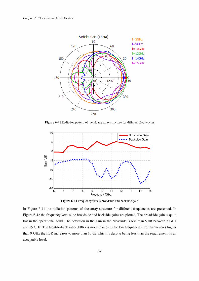
Chapter 6: The Antenna Array Design
82
Figure 6-41 Radiation pattern of the Huang array structure for different frequencies
Figure 6-42 Frequency versus broadside and backside gain
In Figure 6-41 the radiation patterns of the array structure for different frequencies are presented. In
Figure 6-42 the frequency versus the broadside and backside gains are plotted. The broadside gain is quite
flat in the operational band. The deviation in the gain in the broadside is less than 5 dB between 5 GHz
and 15 GHz. The front-to-back ratio (FBR) is more than 6 dB for low frequencies. For frequencies higher
than 9 GHz the FBR increases to more than 10 dB which is despite being less than the requirement, is an
acceptable level.
5 6 7 8 9 10 11 12 13 14 15-20
-15
-10
-5
0
5
10
Frequency [GHz]
Gain
[dB
]
Broadside Gain
Backside Gain
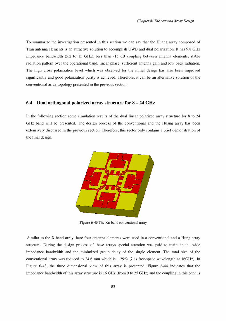
Chapter 6: The Antenna Array Design
83
To summarize the investigation presented in this section we can say that the Huang array composed of
Tran antenna elements is an attractive solution to accomplish UWB and dual polarization. It has 9.8 GHz
impedance bandwidth (5.2 to 15 GHz), less than -15 dB coupling between antenna elements, stable
radiation pattern over the operational band, linear phase, sufficient antenna gain and low back radiation.
The high cross polarization level which was observed for the initial design has also been improved
significantly and good polarization purity is achieved. Therefore, it can be an alternative solution of the
conventional array topology presented in the previous section.
6.4 Dual orthogonal polarized array structure for 8 – 24 GHz
In the following section some simulation results of the dual linear polarized array structure for 8 to 24
GHz band will be presented. The design process of the conventional and the Huang array has been
extensively discussed in the previous section. Therefore, this sector only contains a brief demonstration of
the final design.
Figure 6-43 The Ku-band conventional array
Similar to the X-band array, here four antenna elements were used in a conventional and a Hung array
structure. During the design process of these arrays special attention was paid to maintain the wide
impedance bandwidth and the minimized group delay of the single element. The total size of the
conventional array was reduced to 24.6 mm which is 1.29*λ (λ is free-space wavelength at 16GHz). In
Figure 6-43, the three dimensional view of this array is presented. Figure 6-44 indicates that the
impedance bandwidth of this array structure is 16 GHz (from 9 to 25 GHz) and the coupling in this band is
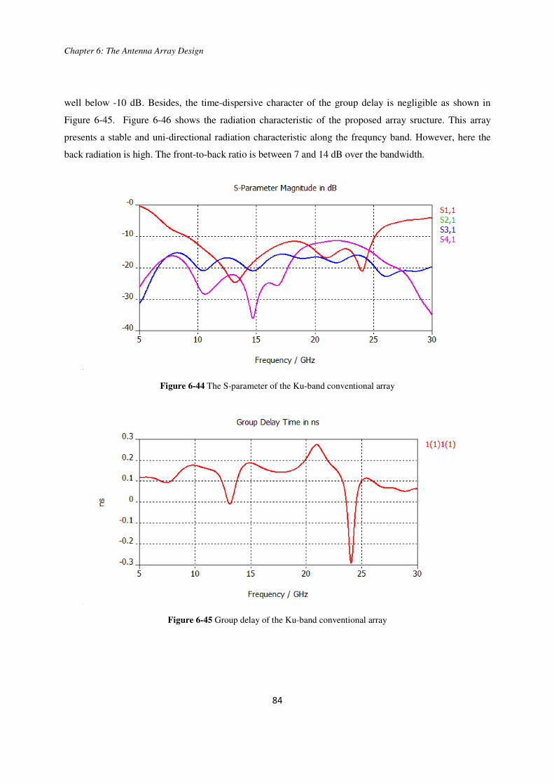
Chapter 6: The Antenna Array Design
84
well below -10 dB. Besides, the time-dispersive character of the group delay is negligible as shown in
Figure 6-45. Figure 6-46 shows the radiation characteristic of the proposed array sructure. This array
presents a stable and uni-directional radiation characteristic along the frequncy band. However, here the
back radiation is high. The front-to-back ratio is between 7 and 14 dB over the bandwidth.
Figure 6-44 The S-parameter of the Ku-band conventional array
Figure 6-45 Group delay of the Ku-band conventional array

Chapter 6: The Antenna Array Design
85
Figure 6-46 Radiation pattern of the Ku-band conventional array for different frequencies
In Figure 6-47, the Ku-band Huang array is presented. Here the size of the sub-array is 20.5 mm which is
1.09*λ (λ is free-space wavelength at 16GHz). Similar to the conventional array, the impedance
bandwidth of this array structure is 16 GHz (from 8.5 to 24.5 GHz) and also the coupling between two
elements is well below -10 dB. Moreover, the group delay deviation is less than half nanosecond as shown
in Figure 6-49.
Figure 6-47 The Ku-band Huang array

Chapter 6: The Antenna Array Design
86
Figure 6-48 The S-parameter of the Ku-band Huang array
Figure 6-49 Group delay of the Ku-band Huang array

Chapter 6: The Antenna Array Design
87
Figure 6-50 Radiation pattern of the Ku-band Huang array for different frequencies
The radiation pattern of the array sructure for different frequency is compared in Figure 6-50. From this
figure it can be concluded that the radiation characteristics is stable in the E plane but in the H plane some
deviation in the pattern is noticed for the higher frequency band. This could be caused by a secondary
mode. Besides, front-to-back ratio is between 5 and 15 dB over the bandwidth which indicats a high back
radiation.
It has been mentioned before that unlike the conventional array, the cross polarization level is not
negligible for the Huang array. In the following figures the polarization purity of the proposed array
structure is demonstrated. At the center frequency (16 GHz) the difference betwen the co and cross
polarization gain is more than 15 dB in the broadside which is an acceptable value. Furthermore, similar
to the X-band Huang array, the cross pol level increases with theta angle in the H plane. However, the
reference polarization is dominating for theta less than 30°.

Chapter 6: The Antenna Array Design
88
Figure 6-51 Co and cross polarized gains of the Ku-band Huang array for the E plane
Figure 6-52 Co and cross polarized gains of the Ku-band Huang array for the H plane
To summarize the research in this section we can say that above simulation results provide enough
evidences that the proposed Ku-band arrays are good solutions for the UWB imaging application. For both
the conventional array shown in Figure 6-43 and the Huang array shown in Figure 6-47 the impedance
bandwidth is 16 GHz which is an extraordinarily large bandwidth for a planar and uni-directional antenna.

Chapter 6: The Antenna Array Design
89
6.5 Fabrication
The antenna elements and antenna arrays designed during this thesis project will be fabricated to verify
the characteristics of the antenna. For that reason, throughout the design procedure practical issues
regarding the manufacturing process, such as tolerance, via diameter and minimum spacing, were
carefully considered. For manufacturing a panel has been created which will be fabricated in near future.
The fabricated designs have the same dimensions as indicated in the previous sections. The top view of
the layout is shown in Figure 6-53. In this layout three types of antenna elements and six types of arrays
are placed. Among the three antenna elements there are the X and the Ku-band antenna element with
surface feeding arrangement and the X-band antenna element with back feeding arrangement. The six
types of arrays consist of two types X-band conventional array, two types X-band Huang array, one type
of Ku-band conventional array and one type Ku-band Huang array. All the antennas and arrays are
designed using a 5.537 mm thick Rogers material. PCB manufacturers do not usually offer boards with
this thickness. Hence, three layers of laminates were combined. On the other side of the substrate a solid
metal ground plane is used.
Figure 6-53 Front view of the fabrication layout

Chapter 6: The Antenna Array Design
90
6.6 Conclusions
In this chapter I have designed four polarimetric UWB arrays: the X-band conventional array, the X-band
Huang array, the Ku-band conventional array and the Ku-band Huang array. The first array type is the X-
band conventional array. For this type of array two solutions are discussed in detail in section 6.2.2. The
first solution has a larger size. Its size is 1.07 times while the later is 0.94 times the free-space wavelength
at the center frequency (10 GHz). These two designs are illustrated in Figure 6-11 and in Figure 6-20. The
second type array was the X-band Huang array. The outcome of this investigation provided more compact
solution where the dimension of the array was only 0.88 times the free-space wavelength at the center
frequency. Both the conventional array and the Huang array showed good results. After that the focus of
this project was placed on Ku-band array design. For this band also a conventional and a Huang array was
designed and both designs showed satisfying outcomes. Results of some additional research on antenna
arrays are shown in Appendix A.

Chapter 7: Conclusion and Recommendations
91
Chapter 7
7 Conclusions and Recommendations
The goal of this master thesis project was to design a dual orthogonal polarized antenna for UWB high
resolution imaging radar. This antenna will enhance the performance of the radar by providing
polarimetric diversity. Furthermore, this antenna should fulfill some additional requirements such as, large
bandwidth, uni-directional pattern, less dispersion, sufficient gain and compact size.
Six different antennas were considered as potential candidates and were carefully investigated. This
investigation provided us a clear overview of the advantages of each candidate along with their
limitations. Based on the comparative study of these antennas, it has been decided that Tran antenna fits in
the best way for the goals of this research.
The original antenna operates in X-band, so a Ku-band antenna has been designed based on the same
principles as the X-band one. The impedance bandwidth of this element is 16 GHz. The size of this
antenna element is half of the free-space wavelength at the centre frequency. Besides, this antenna element
has extremely low group delay, uni-directional pattern and over 90% radiation efficiency.
The original antennas are fed by surface feeding arrangement which is not a suitable feeding for the
applications in mind. Thus a new back feeding structure for the antenna has been investigated, optimized
and implemented. This feeding provides less than -15 dB return loss from very low frequency till up to 16
GHz. By summarizing all the changes in the antenna with respect to the original design I can say that I
have developed a new antenna.

Chapter 7: Conclusion and Recommendations
92
The drawback of Tran antenna is that it transmits a single linear polarization. In order to reach the goals of
the project, a sub-array with four antenna elements has been investigated for dual-orthogonal polarization
implementation. Two different types of arrays were studied – conventional array and Huang array
topologies. The Tran antenna was used to create these two types of arrays for both X-band and Ku-band. I
have designed these arrays by optimizing their topology as well as optimizing the antenna elements
geometry and size. These array structures show very promising features. Firstly, they offer extremely wide
bandwidth. The fractional bandwidth for all these array structures is more than 100%. The impedance
bandwidth for the X-band arrays is about 10GHz and for the Ku-band array is about 16GHz. In recent
time some antenna structures have been published which provides more than 100% fractional bandwidth.
However, the antennas designed in this thesis are unique as they can provide this very wide bandwidth in
combination with the uni-directional pattern (about 10 dB front-to-back ratio) and the planar structure.
Furthermore, these antennas have negligible group delay (sub-nanosecond level), compact size (less than
one free-space wavelength at center frequency) and low cross polarization level (less than -15dB). The
conventional array has the advantage over the Huang array in terms of low cross-pol level. On the other
hand, the Huang array provides better size reduction, less coupling between the elements and therefore
better radiation efficiency.
It was my intension to provide experimental verifications of the simulation results. Hence throughout this
project practical issues regarding the manufacturing process remain under firm consideration. Over the
last six months there were regular contacts with a manufacturer of microwave circuits. In October 2009
data files of the antennas and arrays were sent to this manufacturer for fabrication. Unfortunately due to
their extremely busy schedule the fabrication process is not yet complete. However, in near future all the
antenna elements and antenna arrays presented in this report will be tested at IRCTR. The simulation
results presented in this report were computed with CST. It is a well known simulation tool which has
been developed and tested by many researchers. Therefore, even without the experimental verifications we
can still claim that the results presented in this report are very accurate.
Based on the results presented, one can conclude that the goal of this project - a dual polarized UWB
antenna which can be used for high resolution imaging application, has been reached. I can say that the
antennas designed during this project are exclusive as they posses some antenna characteristics which are
rarely found in the same design.

Chapter 7: Conclusion and Recommendations
93
The future work in the direction of UWB dual-polarized antennas can be carried out in the following
areas:
1. Experimentally verify the simulations results
2. Development of a Tran antenna for S and C band
3. An orthogonal coax-to-coplanar transition which provides good performance up to Ku-band
4. Investigation on the Ku-band Huang array structures to obtain higher front-to-back ratio
5. Further improve the polarization purity and decrease the coupling between the antenna elements

Appendix
94
Appendix A: Some Additional Simulations
Step discontinuity
At the junction of two CPW lines having different widths w1 and w2 an impedance step is formed. Field
discontinuities are introduced due to the increase in current density in the center region and due to the
electric fringing field on the front edge of the wider conductor. These step discontinuities have been
analyzed using finite difference time domain (FDTD) technique in [28]. The equivalent lumped circuit for
this discontinuity can be modeled as a T-network consists of two series inductances (L1, L2), accounting
for the current distortion and a parallel capacitance (C), accounting for the fringing field. The influence of
the capacitance is to lengthen the center conductor line. These equivalent lumped elements are assumed to
be at the plane of the discontinuity. It has been investigated in [29] and [30] that for a fixed metallization
thickness as the step ratio increases both L and C increase. These values can be reduced if instead of a
single step multiple steps are used or even better if a smooth step is used.
Figure A.1 The step and its equivalent lump circuit

Appendix
95
Figure A.2 Step discontinuity of the center conductor of the CPW (a) Smooth step (b) Multi step (c) Single step
Figure A.3 Model of the antenna element with smooth step
Initially in the antenna design a single step was used for the impedance transformer. The effect of a
smooth step was also investigated during this project. Simulation result shows that when the smooth step
was implemented the real part of the input impedance was better match to the 50Ω (Figure A.4).
Furthermore, the inductive and capacitive reactance slightly reduces. These changes of the input
impedance, results a smooth S11 curve which as a result provides less group delay.

Appendix
96
Figure A.4 Input impedances (real part) for the single step and the smooth step
Figure A.5 Return loss for the single step and the smooth step
Figure A.6 Group delay for the single step and the smooth step

Appendix
97
Rectangular slots
There are mainly three major types of coupling between two antenna elements. Lateral coupling (dielectric
coupling), surface coupling and free-space coupling. To reduce the free-space coupling some slots were
placed inside the antenna ring. The results are presented in Figure A. 8. For frequencies between 7 and 18
GHz the average value of S21 is 0.5dB reduced when a=0.1mm and b=0.3mm.
Figure A. 7 Huang Array with slots
Figure A. 8 Coupling between the adjacent elements for different slot size. Here “a” is the width and “b” is the
length of the slots

Appendix
98
Additional vias for the conventional array structure
In chapter 6, antenna arrays were developed to obtain dual polarization. In this chapter it was
demonstrated that it is possible to reduce the size of the X-band conventional array to less than one free-
space wavelength at the center frequency. For this miniaturized array structure, presented in Figure 6-17,
the middle structure was detached from rest of the ground planes. As an additional test, vias were used to
connect this plane to the back ground plane. In Figure A. 9, the simulated models are shown where four
and eight vias are used. Results show that by using these vias we are not achieving much larger bandwidth
and on the contrary the group delay is increasing significantly. Therefore the implementation of via in the
array structure has been avoided in later design.
Figure A. 9 Four (left) or eight (right) vias are used to connected the middle structure to the back ground plane
Figure A. 10 S-parameters of the sub-array in Figure A. 9

Appendix
99
Figure A. 11 S-parameters of the sub-array in Figure A. 9
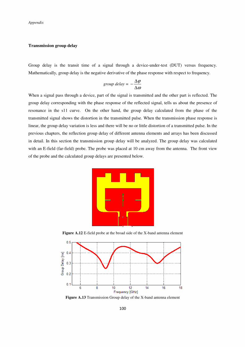
Appendix
100
Transmission group delay
Group delay is the transit time of a signal through a device-under-test (DUT) versus frequency.
Mathematically, group delay is the negative derivative of the phase response with respect to frequency.
group delay = ω
ϕ
∆
∆−
When a signal pass through a device, part of the signal is transmitted and the other part is reflected. The
group delay corresponding with the phase response of the reflected signal, tells us about the presence of
resonance in the s11 curve. On the other hand, the group delay calculated from the phase of the
transmitted signal shows the distortion in the transmitted pulse. When the transmission phase response is
linear, the group delay variation is less and there will be no or little distortion of a transmitted pulse. In the
previous chapters, the reflection group delay of different antenna elements and arrays has been discussed
in detail. In this section the transmission group delay will be analyzed. The group delay was calculated
with an E-field (far-field) probe. The probe was placed at 10 cm away from the antenna. The front view
of the probe and the calculated group delays are presented below.
Figure A.12 E-field probe at the broad side of the X-band antenna element
Figure A.13 Transmission Group delay of the X-band antenna element

Appendix
101
Figure A.14 Transmission group delay of the Ku-band antenna element
Figure A. 15 Transmission group delay of the X-band array presented in Figure 6-20
Figure A. 16 Transmission group delay of the Ku-band array presented in Figure 6-43
From the above graphs we can conclude that the deviation in group delay for the X-band antenna element
is 0.15 ns and for the Ku-band antenna element it is 0.4 ns. For the array structures distortion in the signal
slightly increases. For both the X-band and Ku-band array the maximum deviation in the group delay is
about 0.6 ns. However, the group delay of the X-band array is almost constant between 7 and 18 GHz. For
the Ku-band array we notice some pick in the group delay at 11.5 and 16.5 GHz.

Appendix
102
Appendix B: Selection of the Electromagnetic Solver
In 1886 James C. Maxwell accumulated the Faraday's Law, Ampere's Law and Gauss's Law into a set of
equations which form the basis of EM theory. Maxwell’s equation represents one of the most elegant and
concise ways to state the fundamentals of electricity and magnetism.
Maxwell’s equation in vacuum can be written as [31],
00 =∂+×∇− EH t
rrε
00 =∂+×∇ HE t
rrµ
Where E is the electric field strength (V/m), H is the magnetic field strength (A/m), 0ε is the permittivity
in vacuum (F/m) and 0µ is the permeability in vacuum (H/m).
Analytical solutions of Maxwell’s equations only exist for a very few situations. For all other cases we
approximate the Maxwell’s equation numerically. This is known as the computational electromagnetic
(CEM). In recent time the numerical solution has become an important phase in antenna design. Although
the simulation itself is performed by a computer, some understanding of the numerical method is required
to achieve accurate results.
There are two major types of numerical models- integral method and differential method. Integral methods
(MOM), replaces the radiating/scattering structures by equivalent currents, usually surface currents. These
surface currents are discretized into wire segments or surface patches. A matrix equation is then derived
from which the effect of each segment on every other segment can be found. These interaction are
computed with the use Green function. Green function gives the response in space to a spatially impulsive
current source. Differential methods (FEM, FDTD, TLM), based on the discretization of Maxwell’s
equations over the entire domain and compute the unknown variables over the entire domain [32]. Unlike
integral method here one doesn’t need a green function. Each method has advantages and disadvantages
and the selection is based on accuracy of the solutions, computational time and resources. The proper
choice depends on the type of the problem. The problem of this thesis can be characterized as following-

Appendix
103
Important parameters: The main parameters that we are interested to analysis are the input impedance
and the S-parameters of the antenna. For computing the input impedance, S-parameter, reflection
coefficient etc the FDTD is a good tool. IE might also provide accurate results but the convergence needs
to be checked.
Open problem: We have an open problem. FDTD is good for closed problem where the computational
space is limited by the physical boundaries. For open problem FDTD needs to artificially close the
computation domain by applying boundary or radiation problem. Therefore, IE is more suitable for open
problems.
Homogenous medium: FDTD is more suitable than IE when the media is inhomogeneous. As in our
approximated model we consider that the antenna is in free space, we will get similar accuracy from both
methods.
Far-field: We are interested in the farfield radiation pattern and antenna gain. IE computes these
parameters more accurately. FDTD uses near to far field transformation (NFFT) which can be less
accurate.
Wideband: In our simulation we will need to cover a large frequency band. Integral equation does not
scale linearly with the frequency. The scaling of integral equation is O( 6f ) [32]. Therefore, the
computation time will be much more for integral equation.
Commercially available simulation tool FEKO uses the Method of Moments (MoM) and Computer
Simulation Technology MicroWave Studio (CST MWS) is based on the finite integration technique (FIT)
which is very closely related to FDTD. FEKO is more suitable for open problem and for the computation
of the far-field, while CST is more accurate for calculating the near-field terms such as, input impedance
and S-parameters. However, the main advantage of CST over FEKO for this project was the less
computational time. During this project many array structures are investigated and better computation
efficiency in term of time and memory was essential. Therefore, CST was used as the EM solver for most
analysis in this project.

Bibligraphy
104
Bibliography
[1] J. Taylor, Ed. Introduction to Ultra-wideband Radar Systems. Boca Raton, FL: CRC, 1995
[2] B. Yang, X. Zhuge, A. G. Yarovoy, L.P. Ligthart, “UWB MIMO antenna array topology design using PSO
for through dress near-field imaging”, proc. 5th
European Radar Conference
[3] B. Yang, A. G. Yarovoy, L.P. Ligthart, “UWB Stacked Patch Antenna Design for Near-Field Imaging
Radar Antenna Array”, 3rd
European Conference on Antennas and Propagation, EuCap 2009, pp. 817 - 821
[4] Yunqiang Yang; Fathy, A.E., “See-through-wall imaging using ultra wideband short-pulse radar system”
IEEE trans. on Ant. and Prop, vol. 3B, pp. 334-337, July 2005
[5] Liu, W.; Jafari, H.M.; Hranilovic, S.; Deen, M.J., “Time Domain Analysis of UWB Breast Cancer
Detection”, 23rd
Biennial Symposium on Communications, pp. 336-339, 2006
[6] Chi-Chih Chen; Higgins, M.B.; O'Neill, K.; Detsch, R., “Ultrawide-bandwidth fully-polarimetric ground
penetrating radar classification of subsurface unexploded ordnance”, IEEE trans. On Geoscience and
Remote Sensing, vol. 39, pp. 1221-1230, June 2001
[7] E. Krogager, “Polarimetry: For the Full Story”, NASA no. 19990018202, Denmark, 1998
[8] John D. Dyson, “The Equiangular Spiral Antenna”, IRE Trans. Antennas Propagat., vol. 7, pp. 181 – 187,
April 1959
[9] Julius A. Kaiser, “The Archimedean Two-Wire Spiral Antenna”, IRE Trans. Antennas Propagat., AP-8, pp.
312-323, 1960
[10] John D. Kraus, Ronald J. Merhefka, Antennas for all Application (3rd
Ed.), New York: McGraw-Hill, 2002
[11] Antonije R. Djordjevic, Alenka G. Zajic, Milan M. Ilic and Gordon L. Stuber, “Optimization of Helical
Antenna”, IEEE trans. on Ant. and Prop, Vol. 48, No. 6, December 2006
[12] Egashira, S. and E. Nishiyama, “Stacked microstrip antenna with wide bandwidth and high gain,” IEEE
Trans. Antennas and Prop. Vol. AP-44, 1533–1534, Nov. 1996.
[13] Grzegorg Adamiuk, Jens Timmermann, Werner Wiesbeck, Thomas Zwick “A novel concept of a dual-
orthogonal polarized ultra wideband antenna for medical applications”
[14] Constantine A. Balanis, Antenna Theory: Analysis and Design (3rd
Ed.), New Jersey: John Wiley & Sons,
Inc. 2005
[15] John L. Volakis, Antenna Engineering handbook (4th
Ed.), New York: McGraw-Hill Companies, 2007
[16] D.P. Tran, F.M. Tanyer-Tigrek, I.E Lager, L.P.Ligthart, “A Novel Unidirectional Radiator with Superb
UWB Characteristics for X-band Phased Array Applications”, Proceedings of the European Conference on
Antenna and Propagation: EuCAP 2009
[17] F. M. Tanyer-Tigrek, D. P. Tran, I. E. Lager, L. P. Ligthart, “CPW-fed, quasi magnetic, printed antenna for
ultra wide-band applications”, Scientific Report, IRCTR-S-045-07, 2007

Bibligraphy
105
[18] R.N. Simons (2001), Coplanar Waveguide Circuits, Components and Systems, New York: John Wiley &
Sons, Inc.
[19] Arthur C. Ludwig, “The definition of cross polarization”, IEEE Ant. and Prop, January 1973, pp. 116-119
[20] Marco Sabbadini, Introduction to the design of antennas for space applications, ESTEC reproduction
services, 2006
[21] J. Huang “A technique for an array to generate circular polarization with linear polarized elements”, IEEE
trans. on Ant. and Prop, AP-34, (9), pp. 1113-1124, 1986.
[22] Toshihisa Kamei, Yozo Utsumi, Nguyen Quoc Dinh and Nguyen Thanh, “Wide-band coaxial-to-coplanar
transition” VOL. E90-C, No.10, Oct 2007
[23] E. England, “A coaxial to microstrip transition”, IEEE Trans.Microwave Theory and Tech.vol. MTT-24, pp.
47-48, January 1976
[24] Matthew Morgan and Sander Weinreb, “A millimeter-wave perpendicular coax-to-microstrip transition”,
IEEE MIT-S Intl. Microwave Symp., Seattle, WA, 2002
[25] D. Tallini, A. Galli, M. Ciattaglia, L. Infante, A. De Luca and M. Cicolani, “A new low-profile wide-scan
phased array for UWB applications”, Proc. EuCAP, 11-16 Nov. 2007
[26] A. Galli, G.Valerio, D. Tallini, A. De Luca and M. Cicolani, “Optimization of multifunctional UWB planar
phased arrays”, Proc. EuCAP, Jul. 2009
[27] P.S. Hall, J. Huang, E. Rammos, A. Roederer, “Gain of circularly polarized arrays composed of linearly
polarised elements” Vol. 25, No. 2, Jan 1989
[28] E.Lan, S. M. El-Ghazaly, V.Nair, K. Eisenbeiser and B. Ooms, “Wide band CAD model for coplanar
waveguide using FDTD techniques,” 1997 IEEE Int. Microwave Symp. Dig., Vol. 3, pp. 1583 – 1586,
Denver, CO, June 8-19, 1997
[29] C.W. Chiu and R. B. Wu, “Capacitance computation for CPW discontinuities with finite metallization
thickness by hybrid finite element method” IEEE Trans. Microwave Theory Tech., Vol. 45, pp. 498-504,
April 1997
[30] C.W. Chiu “Inductive computation for CPW discontinuities with finite metallization thickness” IEEE Proc.,
Microwave Antennas Propg., Vol.145, pp. 496-500, Dec 1998
[31] M.D. Verweij, P.M. van den Berg, H. Blok (2001), Electromagnetic waves(2nd
Ed. ), Delft, The
Netherlands: Delft University Press.
[32] D.B. Davidson (2005), Computational Electromagnetics for RF and Microwave Engineering, Cambridge:
Cambridge University Press


![A TWO-PORT ANTENNA FOR WIRELESS-POWERED UWB-RFID … · 2.1. Circularly-Polarized UWB Quasi-Spiral Antenna Spiral antennas [16{18] are widely investigated for UWB antenna designs](https://static.fdocuments.in/doc/165x107/60cd00d2fbca443dcb07fa71/a-two-port-antenna-for-wireless-powered-uwb-rfid-21-circularly-polarized-uwb-quasi-spiral.jpg)