Utilizing Carbon Nanotubes to Improve Efficiency of Organic Solar Cells ENMA 490 Spring 2006.
31
Utilizing Carbon Nanotubes to Improve Efficiency of Organic Solar Cells ENMA 490 Spring 2006
-
Upload
ami-wilkerson -
Category
Documents
-
view
215 -
download
2
Transcript of Utilizing Carbon Nanotubes to Improve Efficiency of Organic Solar Cells ENMA 490 Spring 2006.

Utilizing Carbon Nanotubes to Improve Efficiency of Organic Solar Cells
ENMA 490 Spring 2006
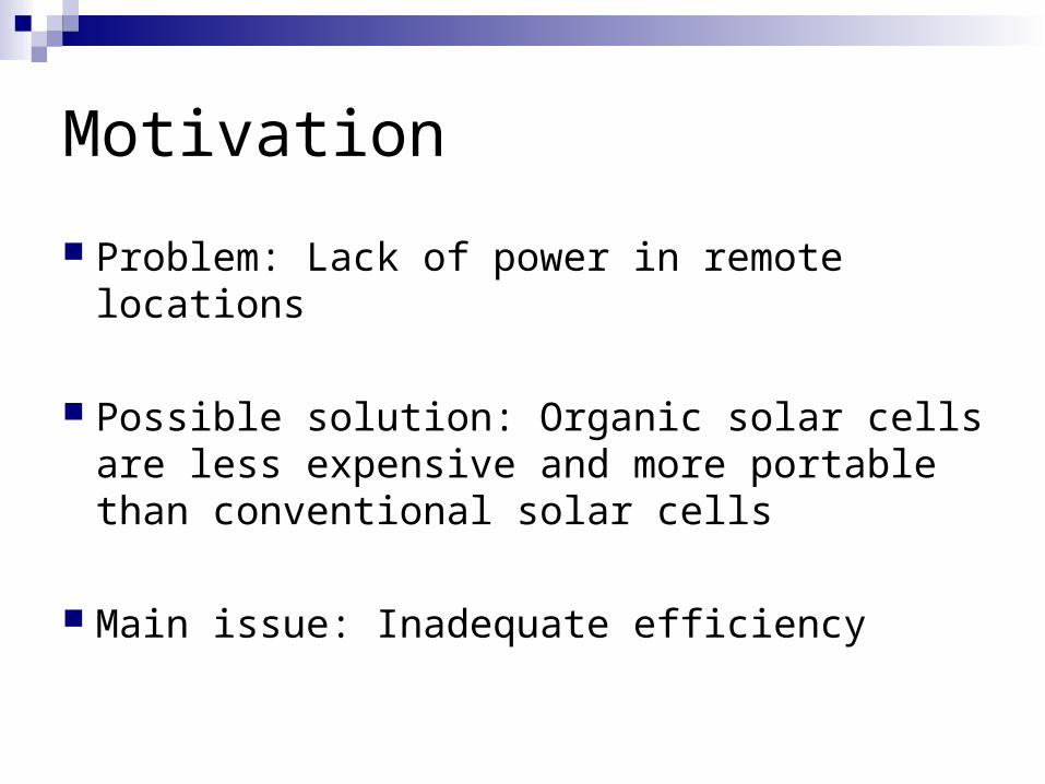
Motivation
Problem: Lack of power in remote locations
Possible solution: Organic solar cells are less expensive and more portable than conventional solar cells
Main issue: Inadequate efficiency
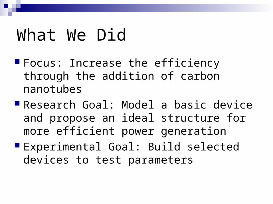
What We Did
Focus: Increase the efficiency through the addition of carbon nanotubes
Research Goal: Model a basic device and propose an ideal structure for more efficient power generation
Experimental Goal: Build selected devices to test parameters

Project Organization
Research TeamErik Lowery Nathan FierroAdam HaughtonRichard Elkins
Experimental TeamErin FlanaganScott WilsonMatt StairMichael Kasser

How Organic Solar Cells Work
High Work Function Electrode
Acceptor Material
Low Work Function Electrode
Donor Material
1. Photon absorption, excitons are created
2. Excitons diffusion to an interface
3. Charge separation due to electric fields at the interface.
4. Separated charges travel to the electrodes.
E
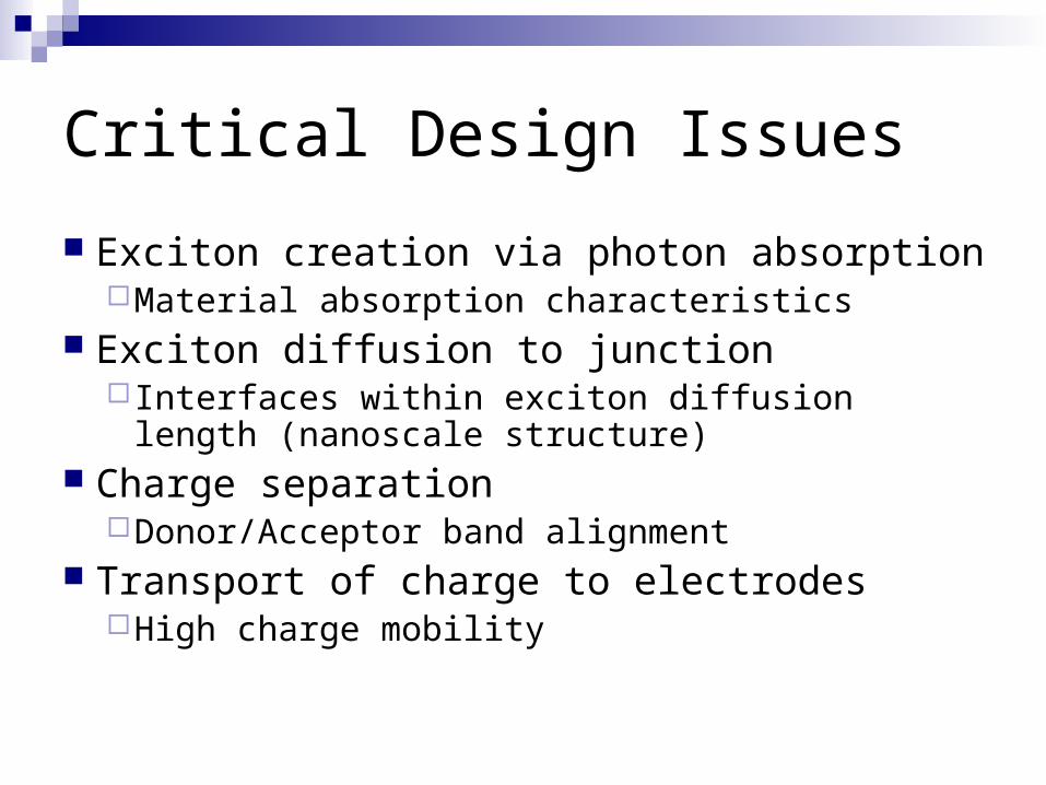
Critical Design Issues
Exciton creation via photon absorptionMaterial absorption characteristics
Exciton diffusion to junction Interfaces within exciton diffusion length (nanoscale
structure) Charge separation
Donor/Acceptor band alignment Transport of charge to electrodes
High charge mobility
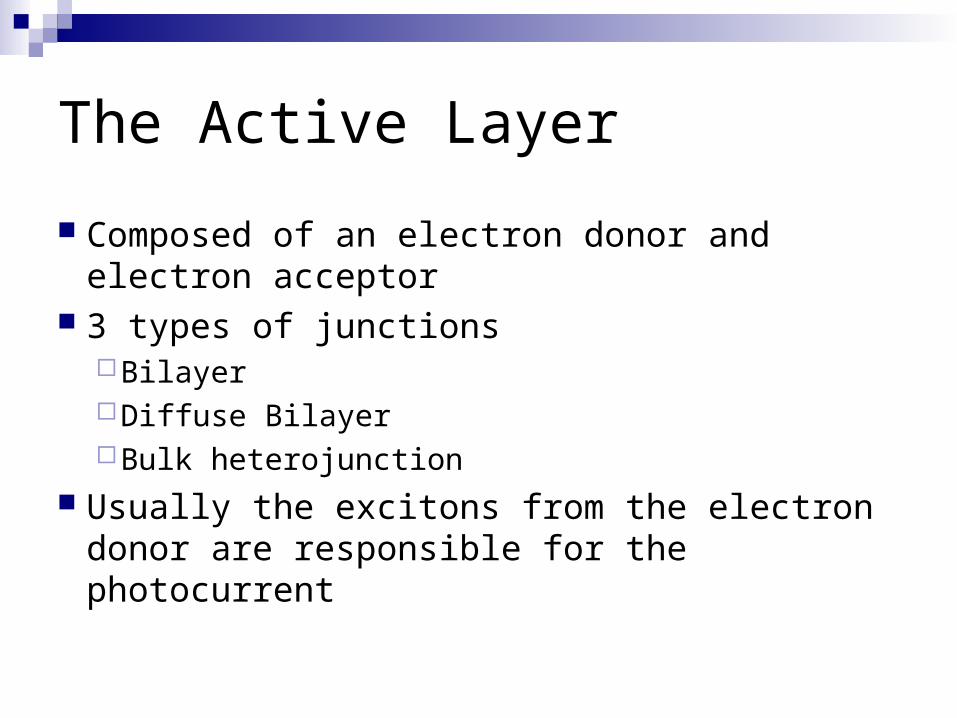
The Active Layer
Composed of an electron donor and electron acceptor
3 types of junctionsBilayerDiffuse BilayerBulk heterojunction
Usually the excitons from the electron donor are responsible for the photocurrent
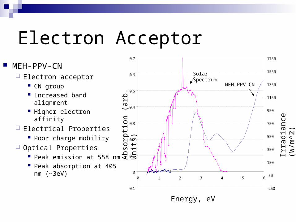
Electron Acceptor MEH-PPV-CN
Electron acceptor CN group Increased band alignment Higher electron affinity
Electrical Properties Poor charge mobility
Optical Properties Peak emission at 558 nm Peak absorption at 405
nm (~3eV)
-0.1
0
0.1
0.2
0.3
0.4
0.5
0.6
0.7
0 1 2 3 4 5 6
-250
-50
150
350
550
750
950
1150
1350
1550
1750
Energy, eV
Irra
dian
ce (
W/m
^2)
Abs
orpt
ion
(arb
. U
nits
) MEH-PPV-CN
Solar Spectrum

Electron Donor Carbon Nanotubes
Orders of magnitude better conductance than polymers
Our nanotubes specifications (Zyvex)
Functionalized Diameter: 5-15 nm Length: 0.5-5 microns MWNT (60% metallic
40% semiconducting)
AFM Amplitude Scan
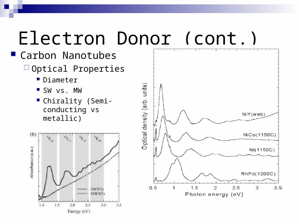
Electron Donor (cont.) Carbon Nanotubes
Optical Properties Diameter SW vs. MW Chirality (Semi-
conducting vs metallic)

Modeling
Model Geometry Photogeneration of Excitons Exciton Transport to Junction Electron Hole Separation Charge Transport to Electrode
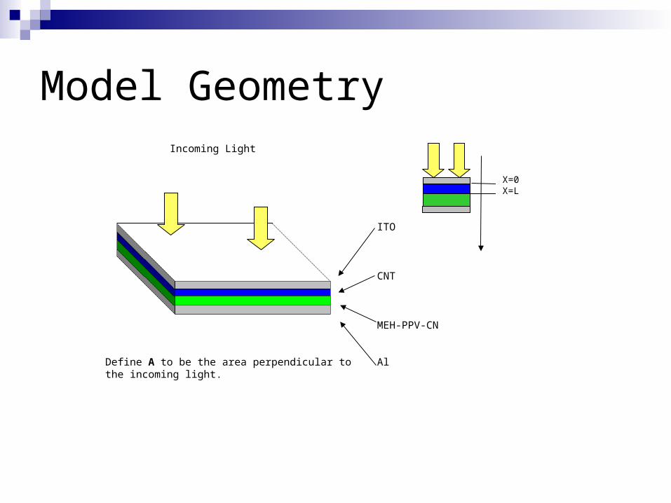
Model Geometry
ITO
CNT
MEH-PPV-CN
Al
Incoming Light
Define A to be the area perpendicular to the incoming light.
X=0X=L
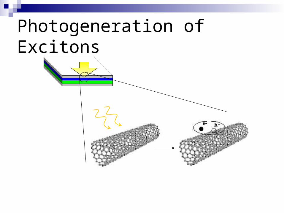
Photogeneration of Excitons
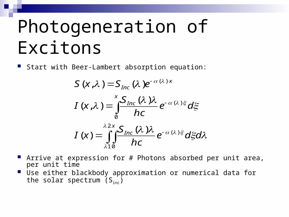
Photogeneration of Excitons
Start with Beer-Lambert absorption equation:
Arrive at expression for # Photons absorbed per unit area, per unit time Use either blackbody approximation or numerical data for the solar
spectrum (Sinc)
2
1 0
)(
0
)(
)(
)()(
)(),(
)(),(
ddehc
SxI
dehc
SxI
eSxS
xInc
xInc
xInc
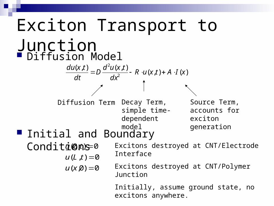
Exciton Transport to Junction Diffusion Model
Initial and Boundary Conditions
)(),(),(),(
2
2
xIAtxuRdx
txudD
dt
txdu
0)0,(
0),(
0),0(
xu
tLu
tu Excitons destroyed at CNT/Electrode Interface
Excitons destroyed at CNT/Polymer Junction
Initially, assume ground state, no excitons anywhere.
Diffusion Term Decay Term, simple time-dependent model
Source Term, accounts for exciton generation
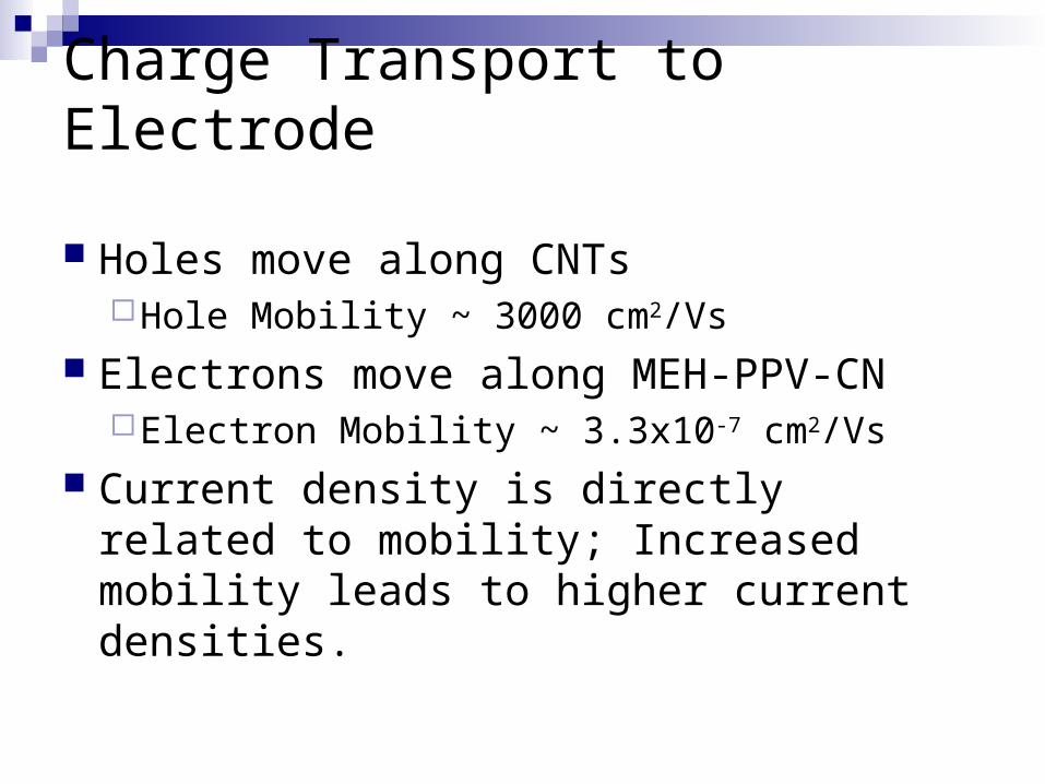
Charge Transport to Electrode
Holes move along CNTsHole Mobility ~ 3000 cm2/Vs
Electrons move along MEH-PPV-CNElectron Mobility ~ 3.3x10⁻⁷ cm2/Vs
Current density is directly related to mobility; Increased mobility leads to higher current densities.

Modeling Summary
CNT/MEH-PPV junctions within diffusion length of exciton generation points
Thickness Optimization Problem:Maximizing thickness gives more excitonsMinimizing thickness leads to higher current
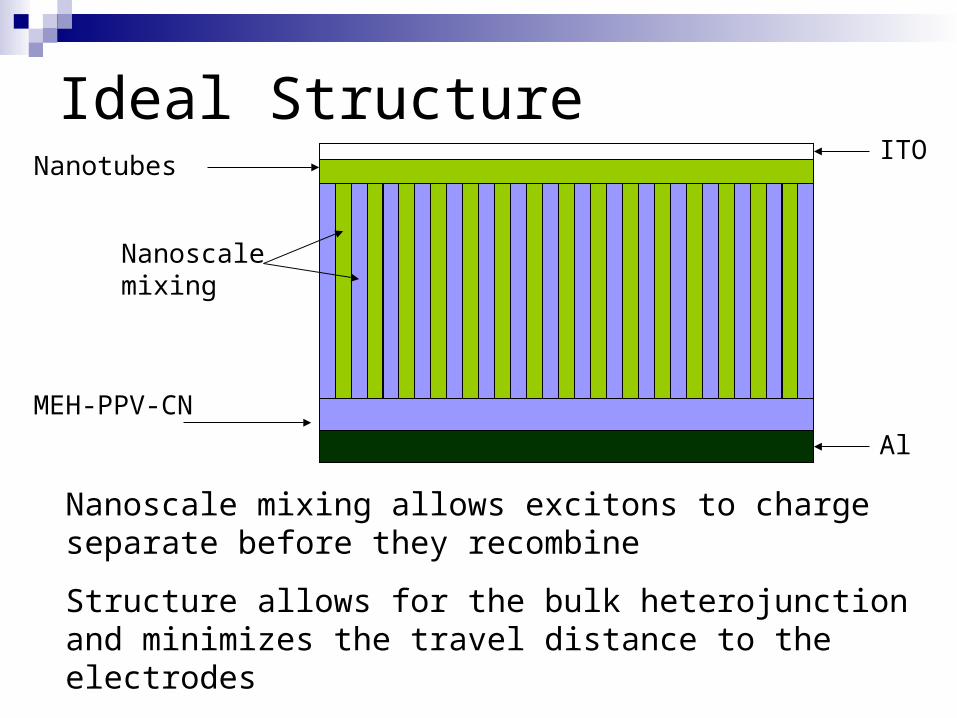
Ideal Structure
Al
MEH-PPV-CN
NanotubesITO
Nanoscale mixing
Nanoscale mixing allows excitons to charge separate before they recombine
Structure allows for the bulk heterojunction and minimizes the travel distance to the electrodes

Experimental Design
Experimental design parametersCNT concentrationMethod of mixingSpin ParametersSolvents

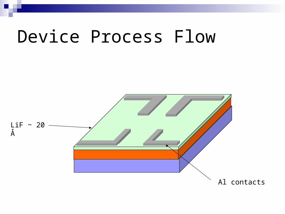
Device Process Flow
ITO
2.5 mm.7 mm
.4 mm
.2 mm

Device Process Flow
PEDOT ~100nm
Al contacts ~600 Å

Active Layer
Device Process Flow
LiF ~ 20 Å
Al contacts
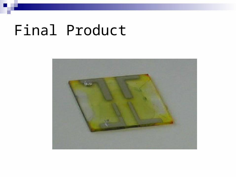
Final Product

Nanotube

Experimental Results
Pure polymer devices acted like diodes. Light emission was observed at higher currents (8 mA)

Experimental Results
Pure CNT acted like a resistor, R >350Ω.
Experimental Design Issues We Addressed Nanotube Processing
Method of dispersionType of solvent
Concentration CNT amount of CNT in solvent CNT to Polymer
Diffused junction vs. bulk heterojunction
Results Summary Absorption spectra measured AFM to check spatial distribution of
nanotubes No successful devices made Possible causes:
CNT shortingFunctionalized CNTs might be a problem

Conclusions
Experimental: Device process recipe needs to be refined Solve experimental design problems to work on
successful device
Modeling: Diffusion model considerations point towards
improving efficiency by creating nanoscale structure Need to consider charge transport in more detail

Acknowledgements
We would like to thank the following people/organizations:Dr. Gary RubloffDr. Danilo RomeroLaboratory for Physical SciencesZyvex