Usingggy SiGe Technology in Extreme Environments - NASA SiGe... · Usingggy SiGe Technology in...
38
Using SiGe Technology in Extreme Environments John D. Cressler Ken Byers Professor School of Electrical and Computer Engineering Georgia Tech, Atlanta, GA 30332 USA [email protected] NASA NEPP Electronics Technology Workshop 2010 John D. Cressler, 6/10 1 NASA-GSFC, Greenbelt, MD 6/24/10 This work was supported by NASA ETDP, NASA-NEPP, DTRA, AFOSR MURI, and JPL
Transcript of Usingggy SiGe Technology in Extreme Environments - NASA SiGe... · Usingggy SiGe Technology in...
Using SiGe Technology g gyin Extreme Environments
John D. CresslerKen Byers Professor
School of Electrical and Computer EngineeringGeorgia Tech, Atlanta, GA 30332 USA
NASA NEPP Electronics Technology Workshop 2010
John D. Cressler, 6/10 1
NASA-GSFC, Greenbelt, MD 6/24/10
This work was supported by NASA ETDP, NASA-NEPP, DTRA, AFOSR MURI, and JPL
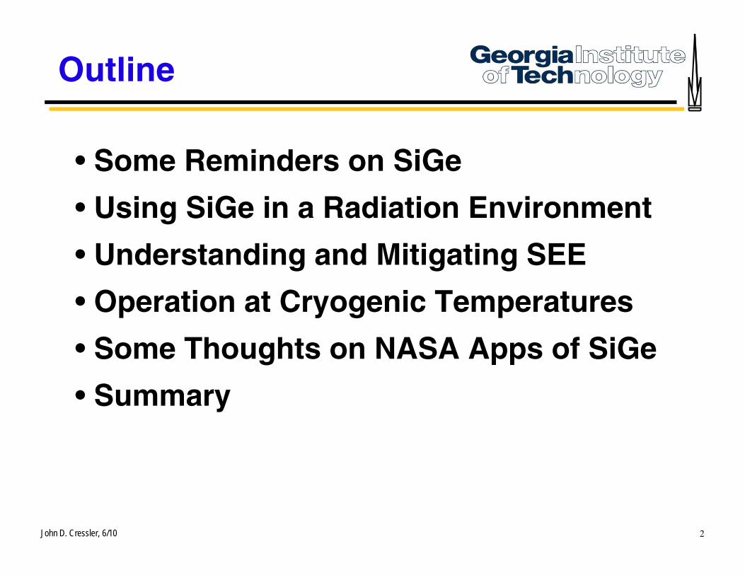
Outline
• Some Reminders on SiGe
• Using SiGe in a Radiation Environment
• Understanding and Mitigating SEE• Understanding and Mitigating SEE
• Operation at Cryogenic Temperatures
• Some Thoughts on NASA Apps of SiGe
• Summary• Summary
John D. Cressler, 6/10 2
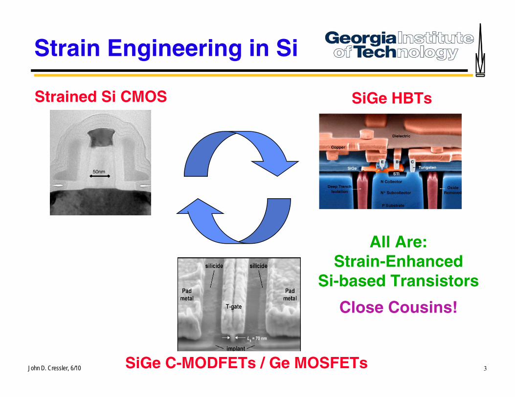
Strain Engineering in Si
Strained Si CMOS SiGe HBTs
All Are:Strain-Enhanced
Si-based Transistors
Close Cousins!
John D. Cressler, 6/10 3SiGe C-MODFETs / Ge MOSFETs
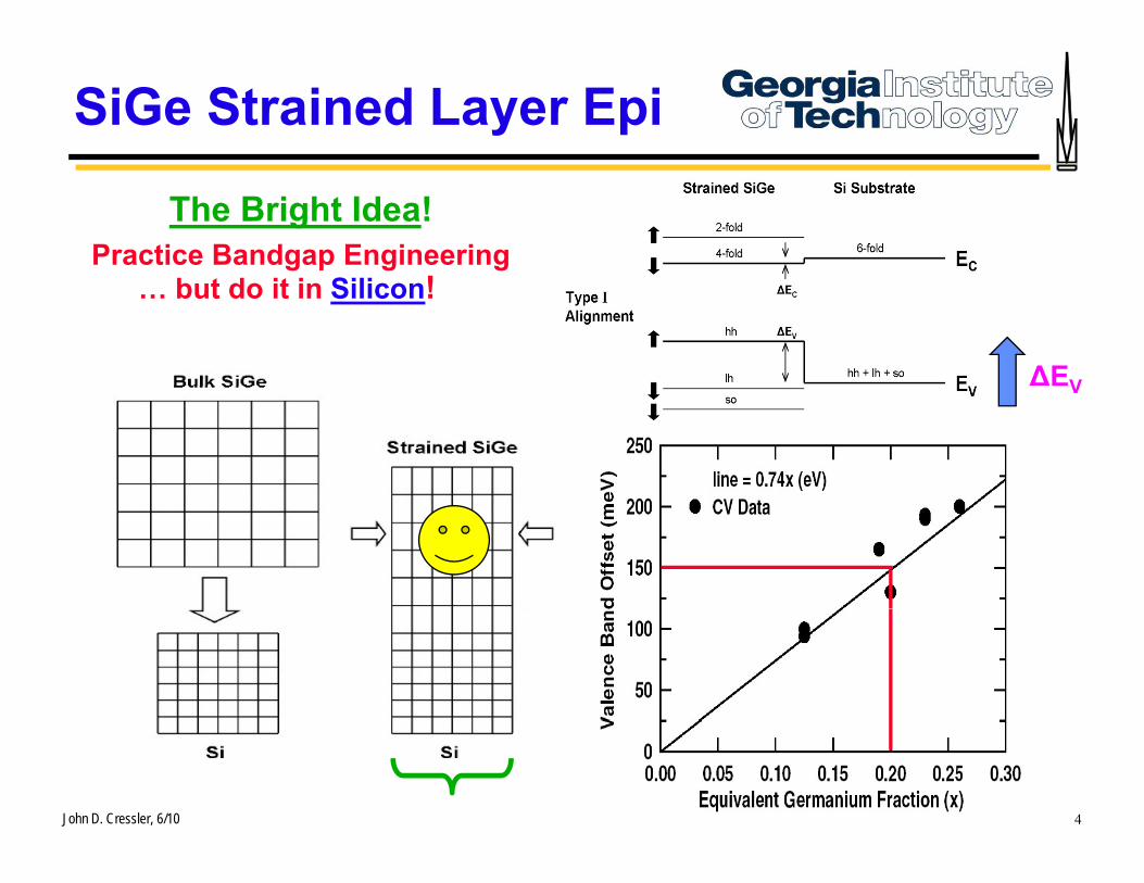
SiGe Strained Layer Epi
Practice Bandgap Engineering The Bright Idea!
… but do it in Silicon!
ΔEVV
John D. Cressler, 6/10 4
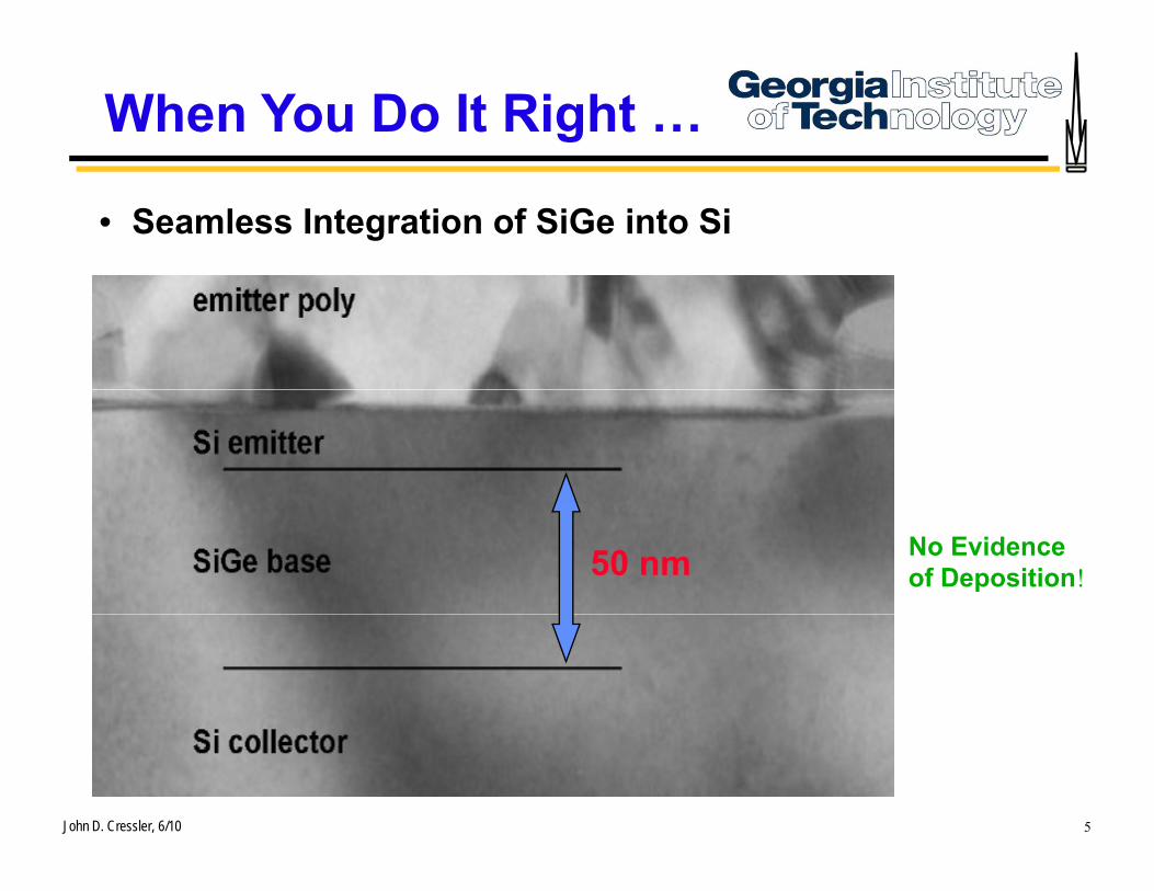
When You Do It Right …
• Seamless Integration of SiGe into Si
No Evidenceof Deposition!50 nm
John D. Cressler, 6/10 5
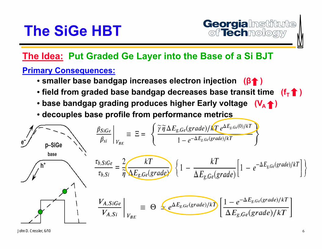
The SiGe HBTThe Idea: Put Graded Ge Layer into the Base of a Si BJTPrimary Consequences:
• smaller base bandgap increases electron injection (β )• field from graded base bandgap decreases base transit time (fT ) • base bandgap grading produces higher Early voltage (VA )• decouples base profile from performance metrics
John D. Cressler, 6/10 6
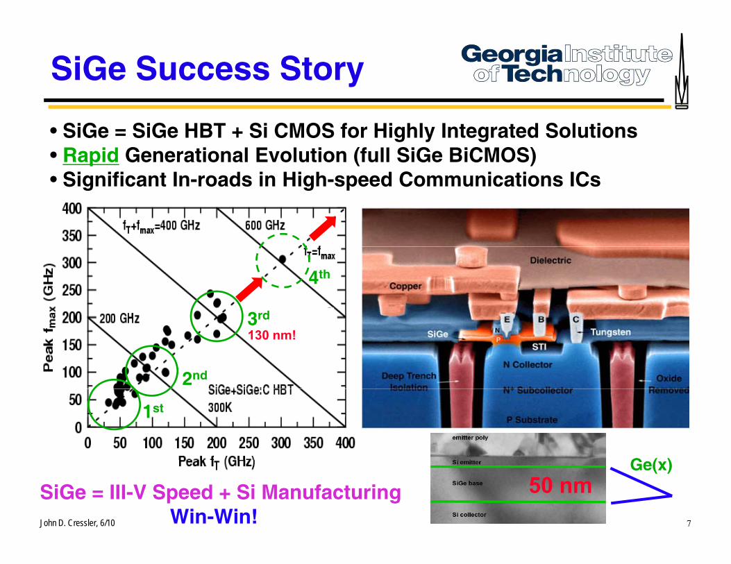
SiGe Success Story
• SiGe = SiGe HBT + Si CMOS for Highly Integrated Solutions• Rapid Generational Evolution (full SiGe BiCMOS)
Significant In roads in High speed Comm nications ICs• Significant In-roads in High-speed Communications ICs
3rd
4th
2nd
3rd
130 nm!
1st
G ( )
John D. Cressler, 6/10 7
SiGe = III-V Speed + Si ManufacturingWin-Win!
50 nmGe(x)
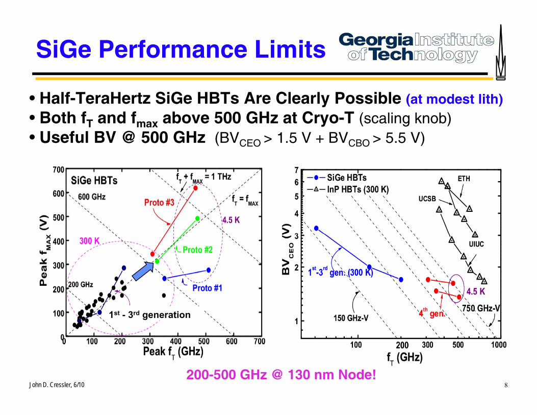
SiGe Performance Limits
• Half-TeraHertz SiGe HBTs Are Clearly Possible (at modest lith)• Both fT and fmax above 500 GHz at Cryo-T (scaling knob) • Useful BV @ 500 GHz (BVCEO > 1.5 V + BVCBO > 5.5 V)
1st - 3rd generation
John D. Cressler, 6/10 8200-500 GHz @ 130 nm Node!
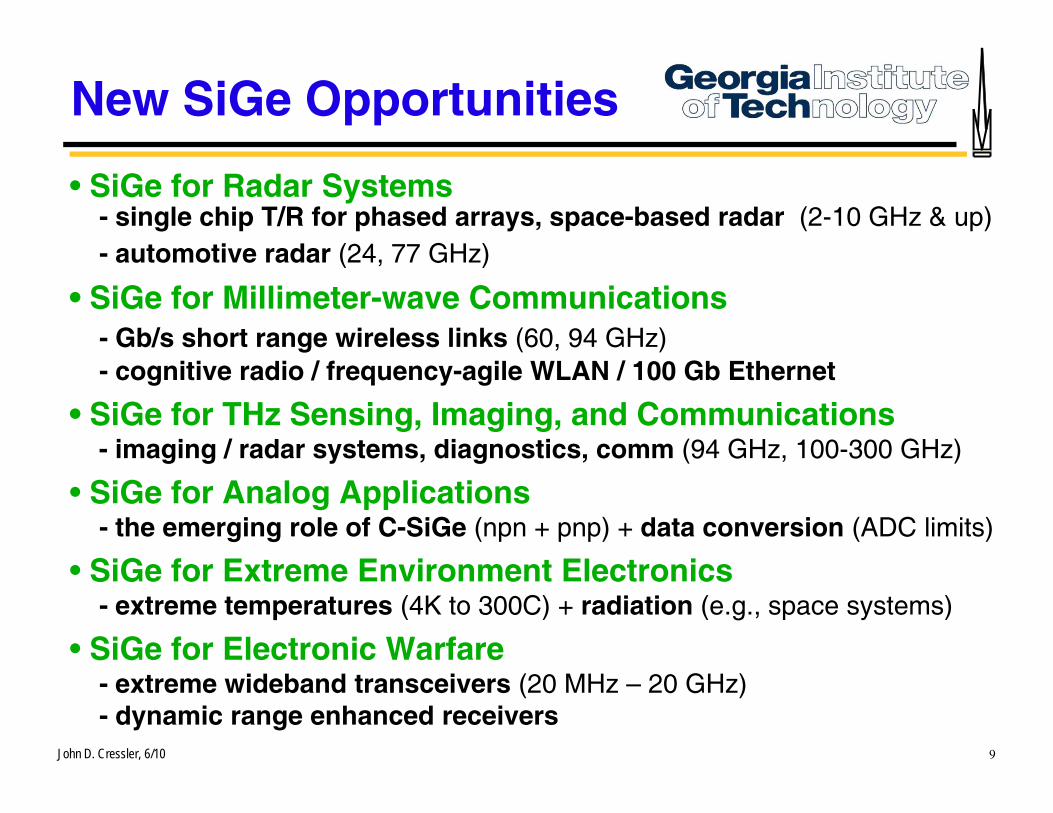
New SiGe Opportunities
• SiGe for Radar Systems- single chip T/R for phased arrays, space-based radar (2-10 GHz & up)
automotive radar (24 77 GHz)- automotive radar (24, 77 GHz)
• SiGe for Millimeter-wave Communications - Gb/s short range wireless links (60, 94 GHz)- cognitive radio / frequency-agile WLAN / 100 Gb Ethernet
• SiGe for THz Sensing, Imaging, and Communications - imaging / radar systems, diagnostics, comm (94 GHz, 100-300 GHz)imaging / radar systems, diagnostics, comm (94 GHz, 100 300 GHz)
• SiGe for Analog Applications- the emerging role of C-SiGe (npn + pnp) + data conversion (ADC limits)
SiG f E t E i t El t i• SiGe for Extreme Environment Electronics- extreme temperatures (4K to 300C) + radiation (e.g., space systems)
• SiGe for Electronic Warfare
John D. Cressler, 6/10 9
- extreme wideband transceivers (20 MHz – 20 GHz)- dynamic range enhanced receivers
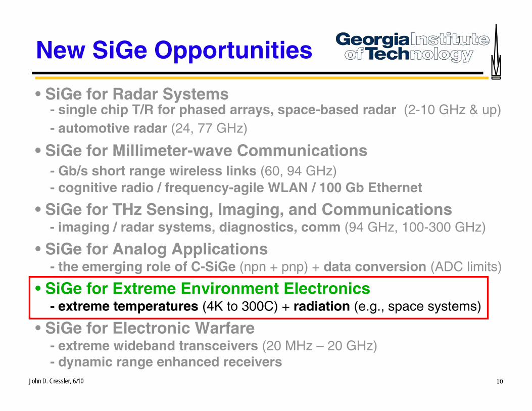
New SiGe Opportunities
• SiGe for Radar Systems- single chip T/R for phased arrays, space-based radar (2-10 GHz & up)
automotive radar (24 77 GHz)- automotive radar (24, 77 GHz)
• SiGe for Millimeter-wave Communications - Gb/s short range wireless links (60, 94 GHz)- cognitive radio / frequency-agile WLAN / 100 Gb Ethernet
• SiGe for THz Sensing, Imaging, and Communications - imaging / radar systems, diagnostics, comm (94 GHz, 100-300 GHz)imaging / radar systems, diagnostics, comm (94 GHz, 100 300 GHz)
• SiGe for Analog Applications- the emerging role of C-SiGe (npn + pnp) + data conversion (ADC limits)
SiG f E t E i t El t i• SiGe for Extreme Environment Electronics- extreme temperatures (4K to 300C) + radiation (e.g., space systems)
• SiGe for Electronic Warfare
John D. Cressler, 6/10 10
- extreme wideband transceivers (20 MHz – 20 GHz)- dynamic range enhanced receivers
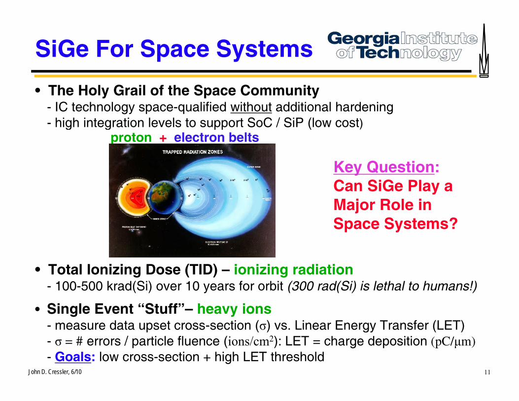
SiGe For Space Systems
• The Holy Grail of the Space Community- IC technology space-qualified without additional hardening- high integration levels to support SoC / SiP (low cost)high integration levels to support SoC / SiP (low cost)
proton + electron belts
Key Question: yCan SiGe Play a Major Role in Space Systems?Space Systems?
• Total Ionizing Dose (TID) – ionizing radiationg ( ) g- 100-500 krad(Si) over 10 years for orbit (300 rad(Si) is lethal to humans!)
• Single Event “Stuff”– heavy ions- measure data upset cross-section (σ) vs Linear Energy Transfer (LET)
John D. Cressler, 6/10 11
measure data upset cross section (σ) vs. Linear Energy Transfer (LET)- σ = # errors / particle fluence (ions/cm2): LET = charge deposition (pC/μm)- Goals: low cross-section + high LET threshold

John D. Cressler, 6/10 12
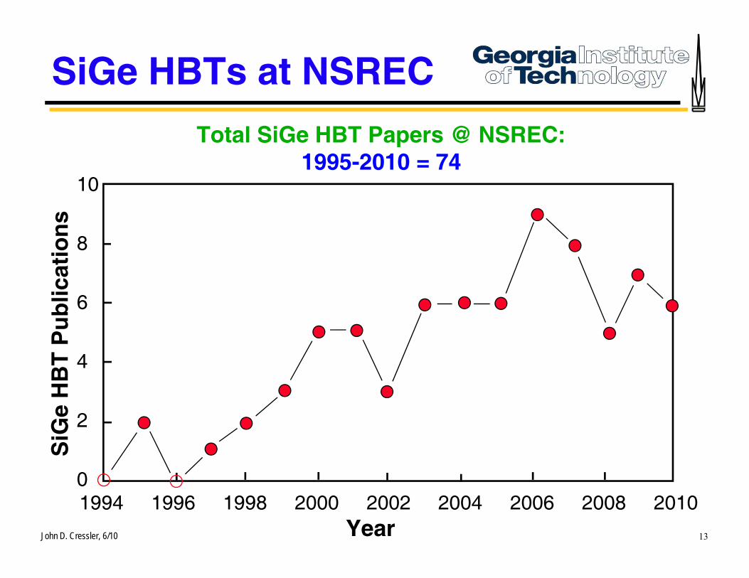
SiGe HBTs at NSREC
10
Total SiGe HBT Papers @ NSREC: 1995-2010 = 74
10
8ion
s
6
ub
licat
i
4
HB
T P
u
2
SiG
e
John D. Cressler, 6/10 13
1994 1996 1998 2000 2002 2004 2006 2008 20100
Year
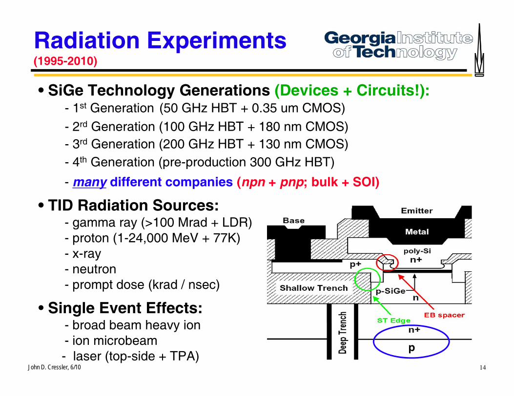
Radiation Experiments (1995-2010)
• SiGe Technology Generations (Devices + Circuits!):- 1st Generation (50 GHz HBT + 0.35 um CMOS)
2rd G ti (100 GH HBT 180 CMOS)- 2rd Generation (100 GHz HBT + 180 nm CMOS)- 3rd Generation (200 GHz HBT + 130 nm CMOS)- 4th Generation (pre-production 300 GHz HBT)
- many different companies (npn + pnp; bulk + SOI)
• TID Radiation Sources:- gamma ray (>100 Mrad + LDR)- gamma ray (>100 Mrad + LDR)- proton (1-24,000 MeV + 77K) - x-ray- neutronneutron- prompt dose (krad / nsec)
• Single Event Effects:broad beam heavy ion
John D. Cressler, 6/10 14
- broad beam heavy ion - ion microbeam- laser (top-side + TPA)
p
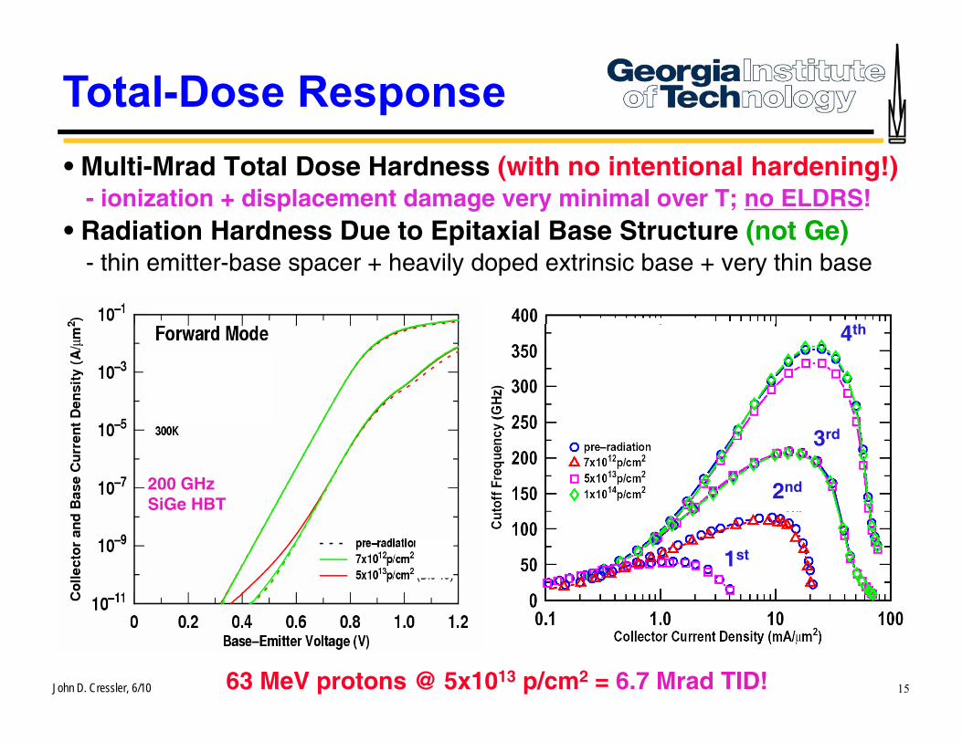
Total-Dose Response• Multi-Mrad Total Dose Hardness (with no intentional hardening!)
- ionization + displacement damage very minimal over T; no ELDRS!• Radiation Hardness Due to Epitaxial Base Structure (not Ge)• Radiation Hardness Due to Epitaxial Base Structure (not Ge)
- thin emitter-base spacer + heavily doped extrinsic base + very thin base
h4th
200 GHz SiGe HBT
3rd
2nd
1st
John D. Cressler, 6/10 1563 MeV protons @ 5x10¹³ p/cm2 = 6.7 Mrad TID!
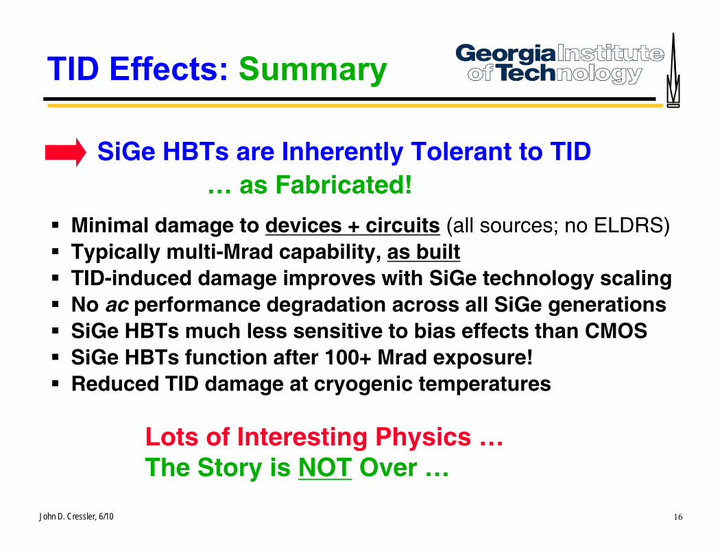
TID Effects: Summary
SiGe HBTs are Inherently Tolerant to TID… as Fabricated!
Minimal damage to devices + circuits (all sources; no ELDRS)Typically multi-Mrad capability, as builtTID-induced damage improves with SiGe technology scalingNo ac performance degradation across all SiGe generationsp g gSiGe HBTs much less sensitive to bias effects than CMOSSiGe HBTs function after 100+ Mrad exposure! Reduced TID damage at cryogenic temperaturesReduced TID damage at cryogenic temperatures
Lots of Interesting Physics …
John D. Cressler, 6/10 16
The Story is NOT Over …
Outline
• Some Reminders on SiGe
• Using SiGe in a Radiation Environment
• Understanding and Mitigating SEE• Understanding and Mitigating SEE
• Operation at Cryogenic Temperatures
• Some Thoughts on NASA Apps of SiGe
• Summary• Summary
John D. Cressler, 6/10 17
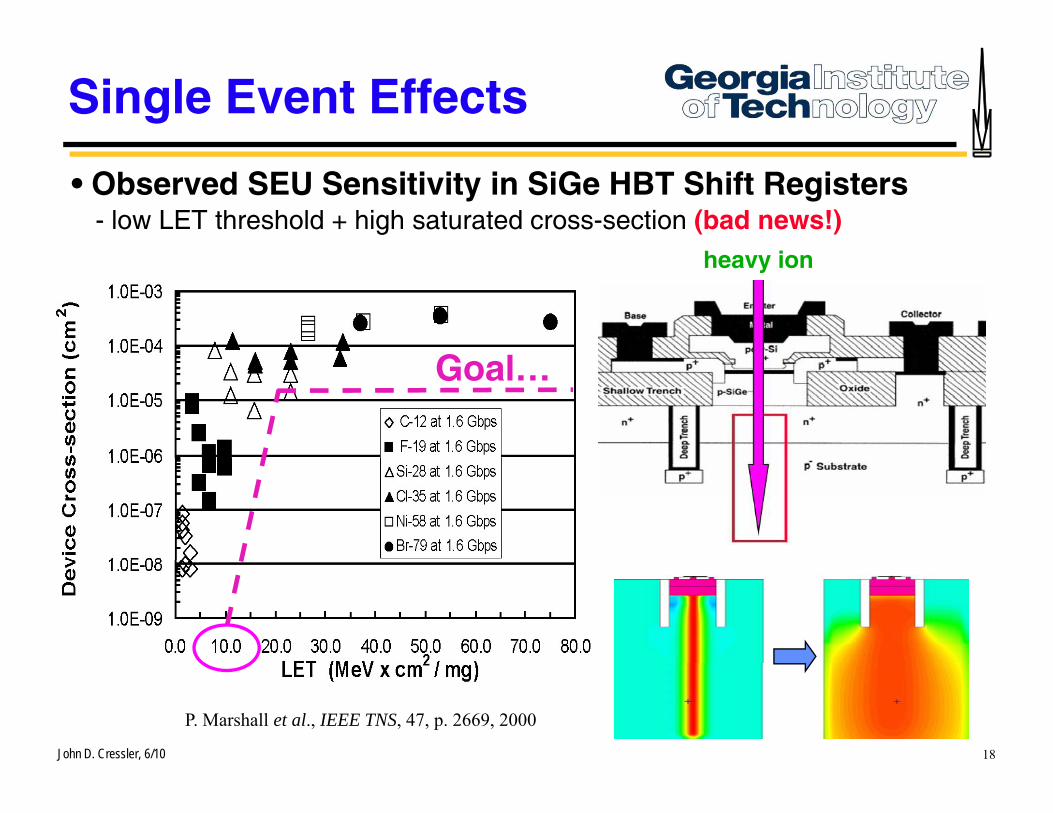
Single Event Effects
• Observed SEU Sensitivity in SiGe HBT Shift Registers- low LET threshold + high saturated cross-section (bad news!)
h i
G l
heavy ion
Goal…
John D. Cressler, 6/10 18
P. Marshall et al., IEEE TNS, 47, p. 2669, 2000
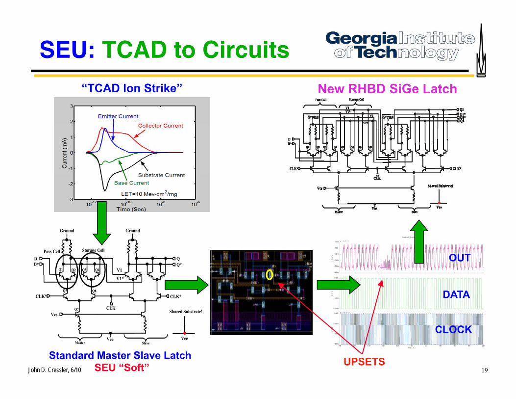
SEU: TCAD to Circuits“TCAD Ion Strike” New RHBD SiGe Latch
OUT
DATA
C OC
John D. Cressler, 6/10 19
CLOCK
Standard Master Slave Latch UPSETSSEU “Soft”
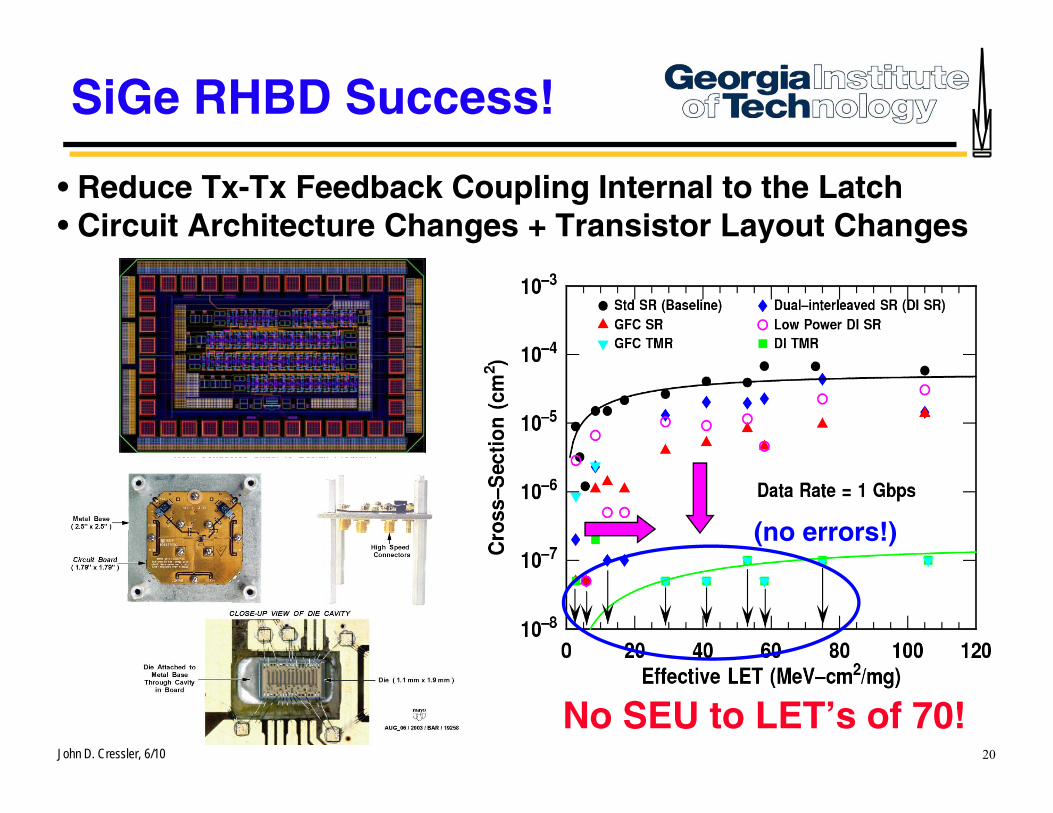
SiGe RHBD Success!
• Reduce Tx-Tx Feedback Coupling Internal to the Latch• Circuit Architecture Changes + Transistor Layout Changes
(no errors!)
John D. Cressler, 6/10 20
No SEU to LET’s of 70!
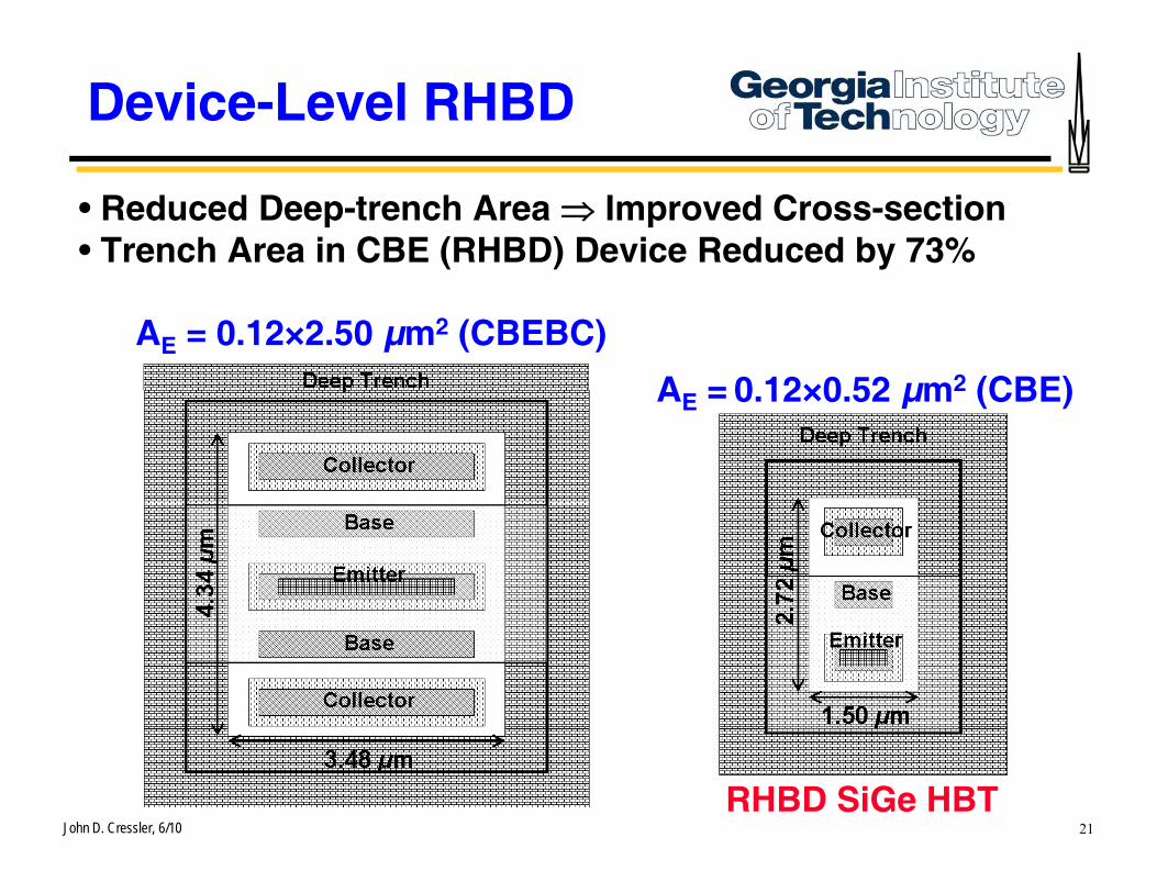
Device-Level RHBD
• Reduced Deep-trench Area ⇒ Improved Cross-section• Trench Area in CBE (RHBD) Device Reduced by 73%
AE = 0.12×2.50 µm2 (CBEBC)
A = 0 12×0 52 µm2 (CBE)AE = 0.12×0.52 µm2 (CBE)
John D. Cressler, 6/10 21RHBD SiGe HBT
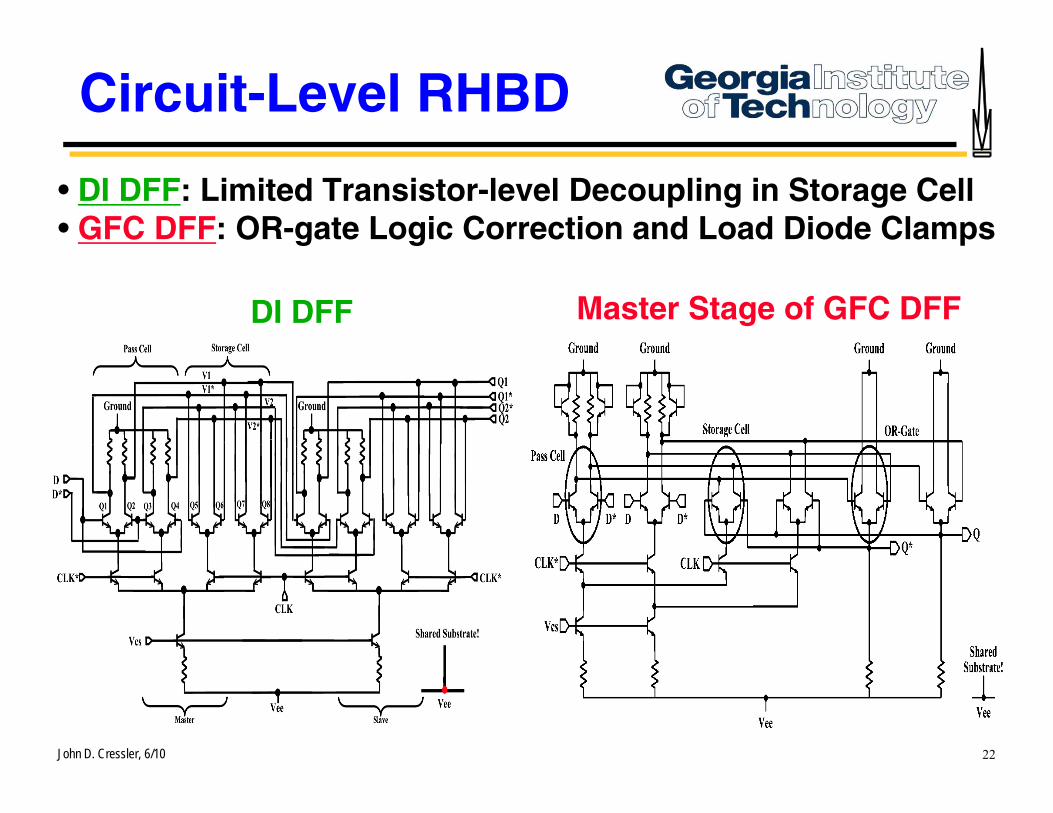
Circuit-Level RHBD
• DI DFF: Limited Transistor-level Decoupling in Storage Cell• GFC DFF: OR-gate Logic Correction and Load Diode Clamps
Master Stage of GFC DFFDI DFF
John D. Cressler, 6/10 22
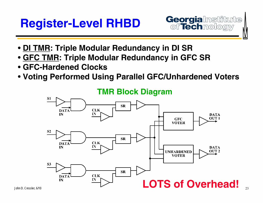
Register-Level RHBD
• DI TMR: Triple Modular Redundancy in DI SR• GFC TMR: Triple Modular Redundancy in GFC SR• GFC-Hardened Clocks• Voting Performed Using Parallel GFC/Unhardened Voters
TMR Bl k DiTMR Block Diagram
John D. Cressler, 6/10 23LOTS of Overhead!
Can We Eliminate TMR
and Still SEE-Harden SiGe?
John D. Cressler, 6/10 24
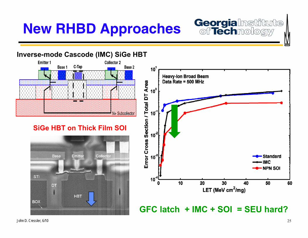
New RHBD Approaches
Inverse-mode Cascode (IMC) SiGe HBT
SiGe HBT on Thick Film SOI
John D. Cressler, 6/10 25
GFC latch + IMC + SOI = SEU hard?
Outline
• Some Reminders on SiGe
• Using SiGe in a Radiation Environment
• Understanding and Mitigating SEE• Understanding and Mitigating SEE
• Operation at Cryogenic Temperatures
• Some Thoughts on NASA Apps of SiGe
• Summary• Summary
John D. Cressler, 6/10 26
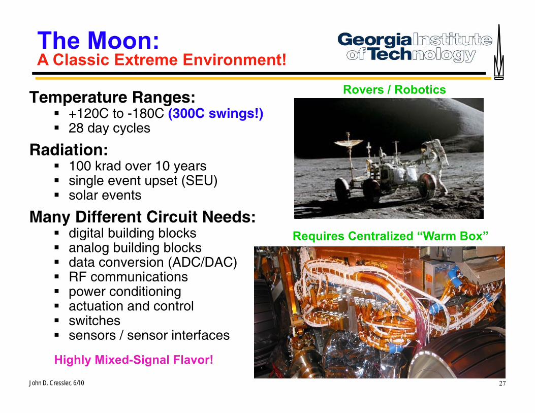
The Moon:A Classic Extreme Environment!
Temperature Ranges:+120C to -180C (300C swings!)28 day cycles
Rovers / Robotics
28 day cycles
Radiation:100 krad over 10 yearssingle event upset (SEU)single event upset (SEU)solar events
Many Different Circuit Needs:digital building blocks R i C t li d “W B ”digital building blocksanalog building blocksdata conversion (ADC/DAC)RF communications
Requires Centralized “Warm Box”
power conditioningactuation and controlswitchessensors / sensor interfaces
John D. Cressler, 6/10 27
sensors / sensor interfaces
Highly Mixed-Signal Flavor!
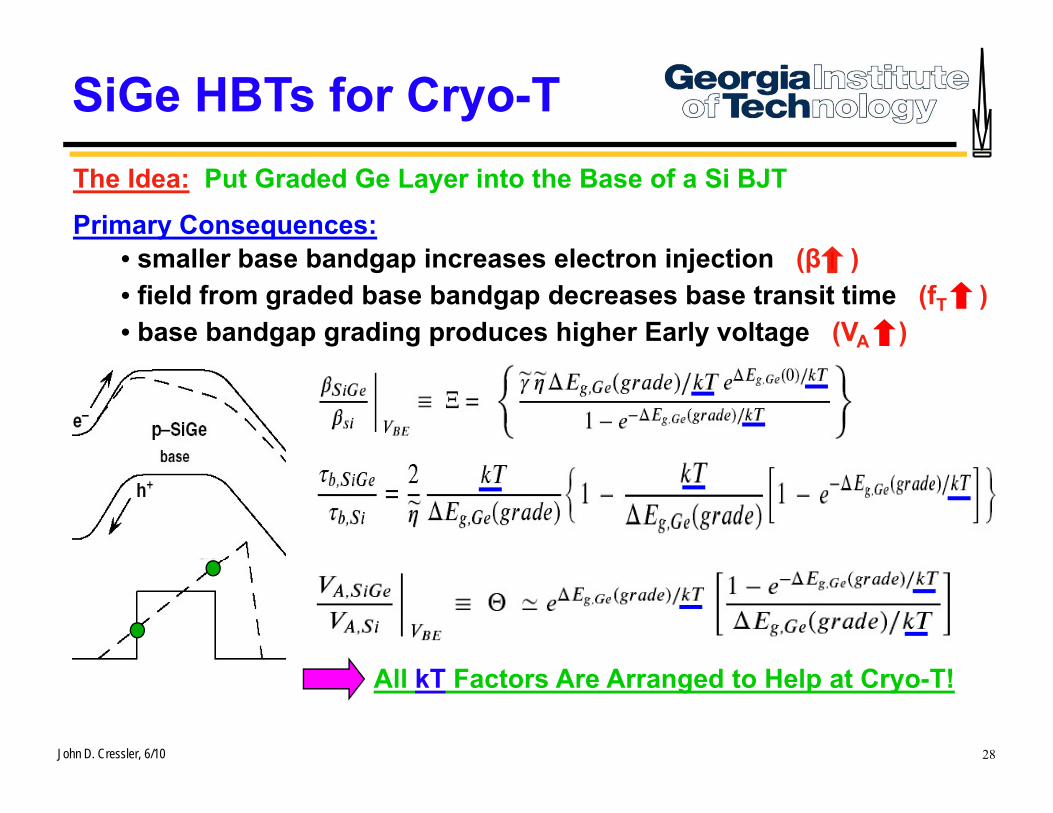
SiGe HBTs for Cryo-TThe Idea: Put Graded Ge Layer into the Base of a Si BJT
Primary Consequences:ll b b d i l t i j ti (β )• smaller base bandgap increases electron injection (β )
• field from graded base bandgap decreases base transit time (fT )• base bandgap grading produces higher Early voltage (VA )
John D. Cressler, 6/10 28
All kT Factors Are Arranged to Help at Cryo-T!
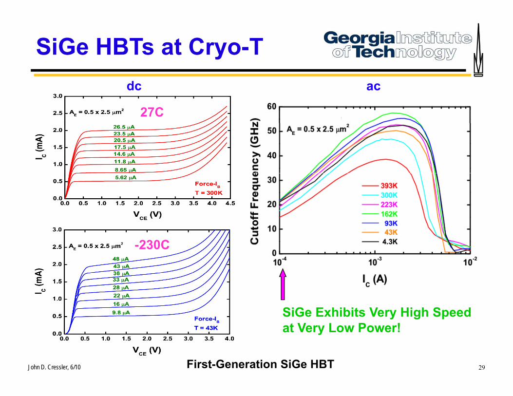
SiGe HBTs at Cryo-T
27C
dc ac
-230C
SiGe Exhibits Very High Speed V P !
John D. Cressler, 6/10 29
at Very Low Power!
First-Generation SiGe HBT
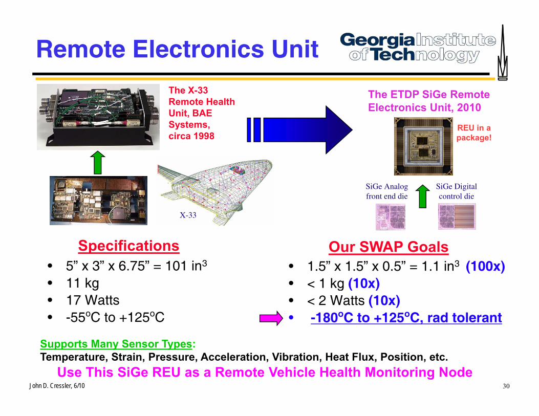
Remote Electronics UnitThe X-33 Remote Health Unit, BAE Systems,
The ETDP SiGe Remote Electronics Unit, 2010
REU in aycirca 1998
REU in a package!
SiGe Analog front end die
SiGe Digital control die
X-33
• 5” x 3” x 6.75” = 101 in3
• 11 kg• 1.5” x 1.5” x 0.5” = 1.1 in3 (100x)• < 1 kg (10x)
Specifications Our SWAP Goals
11 kg• 17 Watts • -55oC to +125oC
< 1 kg (10x)• < 2 Watts (10x)• -180oC to +125oC, rad tolerant
John D. Cressler, 6/10 30
Supports Many Sensor Types:Temperature, Strain, Pressure, Acceleration, Vibration, Heat Flux, Position, etc.
Use This SiGe REU as a Remote Vehicle Health Monitoring Node
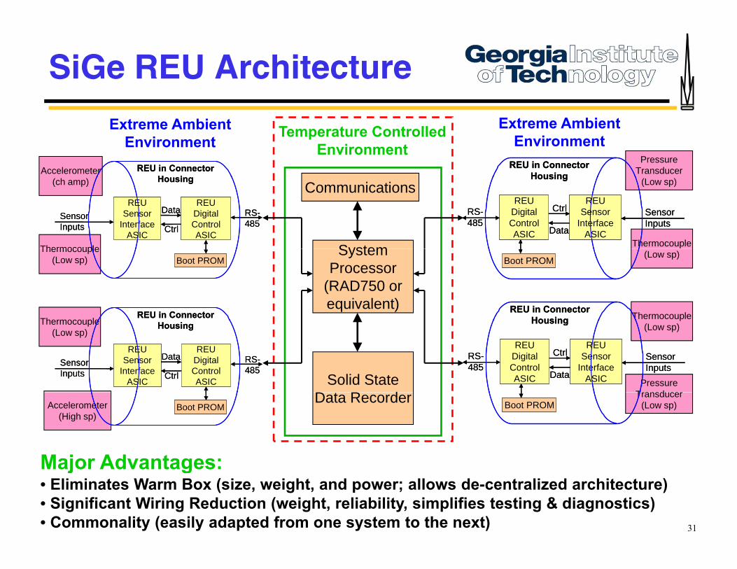
SiGe REU Architecture
Temperature Controlled Environment
Extreme Ambient Environment
Extreme Ambient Environment
Accelerometer Pressure
Transducer REU in Connector Housing
REU in Connector Housing
REU in Connector H i
REU in Connector H i
System
Communications(ch amp)
Thermocouple Thermocouple
(Low sp)
REU Digital Control ASIC
REU Sensor
Interface ASIC
Ctrl
Data
Sensor Inputs
RS-485
Housing
REU Digital Control ASIC
REU Sensor
Interface ASIC
Ctrl
Data
Sensor Inputs
RS-485
Housing
REU Sensor
Interface ASIC
REU Digital Control ASIC
Data
CtrlSensor Inputs
RS-485
Housing
REU Sensor
Interface ASIC
REU Digital Control ASIC
Data
CtrlSensor Inputs
RS-485
Housing
System Processor
(RAD750 or equivalent)
Thermocouple (Low sp)
Thermocouple Thermocouple
(Low sp)Boot PROMBoot PROM
REU in Connector Housing
REU in Connector Housing
Boot PROMBoot PROM
REU in Connector REU in Connector
Solid State D t R d
Thermocouple (Low sp)
p(Low sp)
Pressure Transd cer
REU Digital Control ASIC
REU Sensor
Interface ASIC
Ctrl
Data
Sensor Inputs
RS-485
Housing
REU Digital Control ASIC
REU Sensor
Interface ASIC
Ctrl
Data
Sensor Inputs
RS-485
Housing
REU Sensor
Interface ASIC
REU Digital Control ASIC
Data
CtrlSensor Inputs
RS-485
Housing
REU Sensor
Interface ASIC
REU Digital Control ASIC
Data
CtrlSensor Inputs
RS-485
Housing
Data RecorderAccelerometer (High sp)
Transducer (Low sp)Boot PROMBoot PROMBoot PROMBoot PROM
Major Advantages:
John D. Cressler, 6/10 31
Major Advantages:• Eliminates Warm Box (size, weight, and power; allows de-centralized architecture)• Significant Wiring Reduction (weight, reliability, simplifies testing & diagnostics)• Commonality (easily adapted from one system to the next)
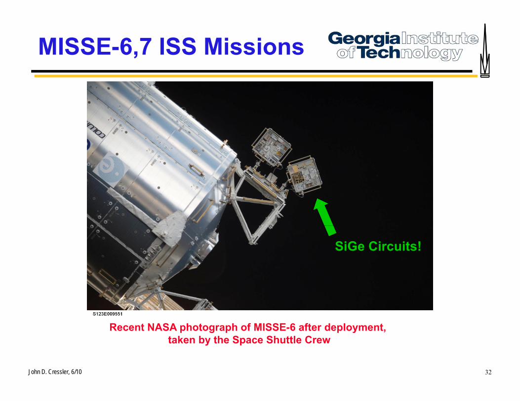
MISSE-6,7 ISS Missions
SiGe Circuits!
Recent NASA photograph of MISSE 6 after deployment
John D. Cressler, 6/10 32
Recent NASA photograph of MISSE-6 after deployment, taken by the Space Shuttle Crew
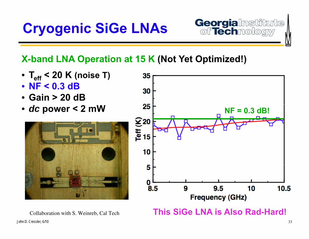
Cryogenic SiGe LNAs
X-band LNA Operation at 15 K (Not Yet Optimized!)• T < 20 K (noise T)• Teff < 20 K (noise T)• NF < 0.3 dB• Gain > 20 dB• dc power < 2 mW NF = 0.3 dB!
John D. Cressler, 6/10 33
Collaboration with S. Weinreb, Cal Tech This SiGe LNA is Also Rad-Hard!
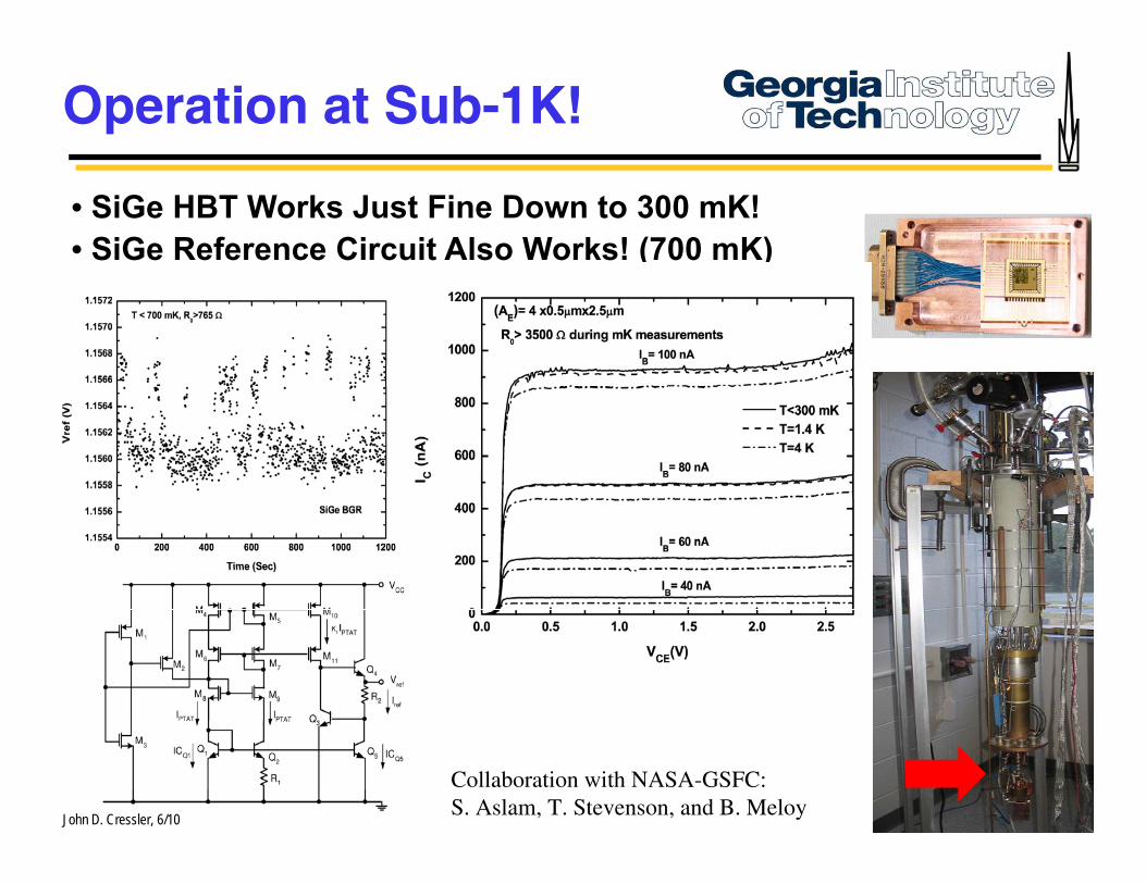
Operation at Sub-1K!
• SiGe HBT Works Just Fine Down to 300 mK!• SiGe Reference Circuit Also Works! (700 mK)
John D. Cressler, 6/10
Collaboration with NASA-GSFC:S. Aslam, T. Stevenson, and B. Meloy
Outline
• Some Reminders on SiGe
• Using SiGe in a Radiation Environment
• Understanding and Mitigating SEE• Understanding and Mitigating SEE
• Operation at Cryogenic Temperatures
• Some Thoughts on NASA Apps of SiGe
• Summary• Summary
John D. Cressler, 6/10 35
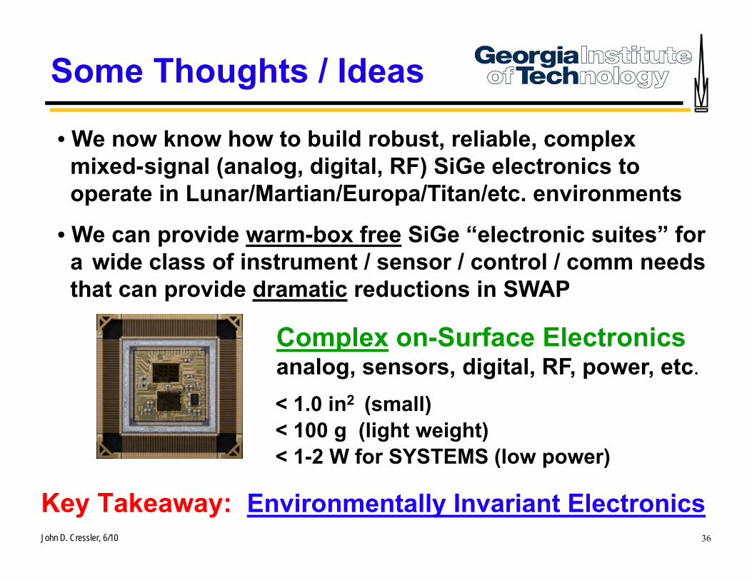
Some Thoughts / Ideas
• We now know how to build robust, reliable, complex mixed-signal (analog, digital, RF) SiGe electronics to operate in Lunar/Martian/Europa/Titan/etc. environments
• We can provide warm-box free SiGe “electronic suites” for id l f i t t / / t l / da wide class of instrument / sensor / control / comm needs
that can provide dramatic reductions in SWAP
< 1 0 i 2 ( ll)
Complex on-Surface Electronicsanalog, sensors, digital, RF, power, etc.
< 1.0 in2 (small)< 100 g (light weight)< 1-2 W for SYSTEMS (low power)
John D. Cressler, 6/10 36
Key Takeaway: Environmentally Invariant Electronics
Summary
• SiGe HBT BiCMOS Technology - combines III-V speed with Si manufacturing (win-win) - many new apps (SiGe is a natural for space environments)
• Using SiGe HBTs in Radiation Environmentsbuilt in total dose hardness (multi Mrad!) - built-in total-dose hardness (multi-Mrad!)
- SEU is an issue to be reckoned with (fast digital = worst case)
• SiGe Technology Can Provide Mission Designers With:- environmentally-invariant electronic suites - warm-box free operation- dramatic reductions in SWAP- improved reliability- commonality of electronic systems
John D. Cressler, 6/10 37
New Ways to Think About NASA Mission Design
Acknowledgement
• Akil Sutton, Stan Phillips, Ryan Diestelhorst, Laleh Najafizadeh, Ted Wilcox, Marco Bellini, Kurt Moen, Aravind Appaswamy, Tushar Thrivikraman, and Tom Cheng (my Georgia Tech team) Tushar Thrivikraman, and Tom Cheng (my Georgia Tech team)
• Guofu Niu and team (Auburn University)• Robert Reed, Ron Schrimpf, and teams (Vanderbilt University)
Pa l Marshall Mart Carts Jonn Pellish and Ken LaBel (NASA GSFC)• Paul Marshall, Marty Carts, Jonny Pellish, and Ken LaBel (NASA-GSFC)• The NASA ETDP SiGe Team, including: Ben Blalock, Wayne Johnson,
Alan Mantooth, Mohammad Mojarradi, Guofu Niu, Foster Dai, Pat McCluskey Leora Peltz Richard Berger Ray Garbos (and teams) Pat McCluskey, Leora Peltz, Richard Berger, Ray Garbos (and teams)
• Lew Cohn and James Fee (DTRA)• Barb Randall and team (Mayo Foundation)y• George Vizkelethy and Paul Dodd (Sandia)• Dale McMorrow (NRL)
• Marek Turowski and team (CFDRC)
John D. Cressler, 6/10 38
• Marek Turowski and team (CFDRC)
• The SiGe Teams at IBM, Jazz, IHP, TI, National, and ST Microand many others …