Using the TPS92561 Off-Line Boost LED Driver (Rev. A)
30
User's Guide SLUUAU9A – December 2013 – Revised January 2014 Using the TPS92561 Off-Line Boost LED Driver The TPS92561EVM is a 12-W maximum, 120-VAC non-isolated dimmable LED driver. The TPS92561EVM implements a dimming solution using the TPS92561 integrated circuit from Texas Instruments. This user's guide provides electrical specifications, performance data, typical characteristic curves, schematics, printed-circuit board layout, and a bill of materials. Contents 1 Introduction .................................................................................................................. 2 2 Description ................................................................................................................... 2 2.1 Typical Applications ................................................................................................ 2 2.2 TPS92561 Features ............................................................................................... 2 3 Electrical Performance Specifications .................................................................................... 3 4 Schematic .................................................................................................................... 4 5 Performance Data and Typical Characteristic Curves ................................................................. 6 5.1 Efficiency ............................................................................................................ 6 5.2 Power Factor ....................................................................................................... 6 5.3 Input Current Total Harmonic Distortion ........................................................................ 7 5.4 Output Ripple ....................................................................................................... 7 5.5 Turn On Waveform ................................................................................................ 8 5.6 Hysteretic Boost PFC Operation ................................................................................. 8 5.7 Dimming – Leviton 6683 Forward Phase Dimmer ............................................................. 9 5.8 Dimming – Lutron Diva 303P Reverse Phase Dimmer ...................................................... 10 5.9 Dimming – Lutron Maestro MAW-600H-LA Electronic Dimmer ............................................ 10 5.10 Dimming – NEMA SSL-6 Compliance ......................................................................... 11 5.11 EMI Scan .......................................................................................................... 12 5.12 Radiated EMI ...................................................................................................... 13 5.13 Dimmer Testing ................................................................................................... 14 6 Reference Design, Assembly Drawing, PCB Layout, and Bill of Materials ........................................ 15 6.1 Reference Design, Assembly Drawing, and PCB Layout ................................................... 15 6.2 Bill of Materials .................................................................................................... 16 Appendix A Detailed Test Setup and Test Data ............................................................................ 18 Appendix B Layout Considerations ........................................................................................... 21 Appendix C EVM Circuit Options Used ...................................................................................... 23 List of Figures 1 TPS92561 Boost Schematic .............................................................................................. 4 2 Dimming Wiring Diagram .................................................................................................. 5 3 TPS92561 Boost Efficiency................................................................................................ 6 4 TPS92561 Boost Input Power Factor .................................................................................... 6 5 TPS92561 Boost Input Current Total Harmonic Distortion ............................................................ 7 6 Output Ripple (V OUT = 215 V, I OUT = 50 mA, THD 7.5%) ............................................................... 7 7 Turn On Waveform, Turn-On Time ≡ 20 ms ............................................................................ 8 8 Hysteretic Control of Boost Inductor Current (at Maximum V ADJ Voltage) ........................................... 8 9 Hysteretic Control of Boost Inductor Current (at Minimum V ADJ Voltage) ............................................ 9 10 Leviton Forward Phase Dimmer (90° Conduction Angle).............................................................. 9 11 Lutron Reverse Phase Dimmer (90° Conduction Angle) ............................................................. 10 1 SLUUAU9A – December 2013 – Revised January 2014 Using the TPS92561 Off-Line Boost LED Driver Submit Documentation Feedback Copyright © 2013–2014, Texas Instruments Incorporated
Transcript of Using the TPS92561 Off-Line Boost LED Driver (Rev. A)
User's GuideSLUUAU9A–December 2013–Revised January 2014
Using the TPS92561 Off-Line Boost LED Driver
The TPS92561EVM is a 12-W maximum, 120-VAC non-isolated dimmable LED driver. TheTPS92561EVM implements a dimming solution using the TPS92561 integrated circuit from TexasInstruments. This user's guide provides electrical specifications, performance data, typical characteristiccurves, schematics, printed-circuit board layout, and a bill of materials.
Contents1 Introduction .................................................................................................................. 22 Description ................................................................................................................... 2
2.1 Typical Applications ................................................................................................ 22.2 TPS92561 Features ............................................................................................... 2
3 Electrical Performance Specifications .................................................................................... 34 Schematic .................................................................................................................... 45 Performance Data and Typical Characteristic Curves ................................................................. 6
5.1 Efficiency ............................................................................................................ 65.2 Power Factor ....................................................................................................... 65.3 Input Current Total Harmonic Distortion ........................................................................ 75.4 Output Ripple ....................................................................................................... 75.5 Turn On Waveform ................................................................................................ 85.6 Hysteretic Boost PFC Operation ................................................................................. 85.7 Dimming – Leviton 6683 Forward Phase Dimmer ............................................................. 95.8 Dimming – Lutron Diva 303P Reverse Phase Dimmer ...................................................... 105.9 Dimming – Lutron Maestro MAW-600H-LA Electronic Dimmer ............................................ 105.10 Dimming – NEMA SSL-6 Compliance ......................................................................... 115.11 EMI Scan .......................................................................................................... 125.12 Radiated EMI ...................................................................................................... 135.13 Dimmer Testing ................................................................................................... 14
6 Reference Design, Assembly Drawing, PCB Layout, and Bill of Materials ........................................ 156.1 Reference Design, Assembly Drawing, and PCB Layout ................................................... 156.2 Bill of Materials .................................................................................................... 16
Appendix A Detailed Test Setup and Test Data ............................................................................ 18Appendix B Layout Considerations ........................................................................................... 21Appendix C EVM Circuit Options Used ...................................................................................... 23
List of Figures
1 TPS92561 Boost Schematic .............................................................................................. 42 Dimming Wiring Diagram .................................................................................................. 53 TPS92561 Boost Efficiency................................................................................................ 64 TPS92561 Boost Input Power Factor .................................................................................... 65 TPS92561 Boost Input Current Total Harmonic Distortion ............................................................ 76 Output Ripple (VOUT = 215 V, IOUT = 50 mA, THD 7.5%) ............................................................... 77 Turn On Waveform, Turn-On Time ≡ 20 ms ............................................................................ 88 Hysteretic Control of Boost Inductor Current (at Maximum VADJ Voltage) ........................................... 89 Hysteretic Control of Boost Inductor Current (at Minimum VADJ Voltage) ............................................ 910 Leviton Forward Phase Dimmer (90° Conduction Angle).............................................................. 911 Lutron Reverse Phase Dimmer (90° Conduction Angle) ............................................................. 10
1SLUUAU9A–December 2013–Revised January 2014 Using the TPS92561 Off-Line Boost LED DriverSubmit Documentation Feedback
Copyright © 2013–2014, Texas Instruments Incorporated
Introduction www.ti.com
12 Lutron Forward Phase Electronic Dimmer (90° Conduction Angle) ................................................ 1013 NEMA SSL-6 Compliance Data Based on Forward Phase – Leviton 6683, Reverse Phase Dimmer –
Lutron Diva 303P, and Electronic Dimmer - Lutron Maestro MAW-600H-LA Dimmer ........................... 1114 Conducted EMI Scan ..................................................................................................... 1215 Amplitude vs Frequency, R10 = 100 Ω and C9 = 0.1 µF ............................................................ 1316 PCB 3D Top View ......................................................................................................... 1517 TPS92561 Boost Top (Left) and Bottom (Right) Layer Assembly Drawing........................................ 1518 TPS92561 Boost Top (Left) and Bottom (Right) Copper Layer ..................................................... 1519 Suggested Dimming Connection ........................................................................................ 1820 Critical Current Paths in Boost Topology............................................................................... 2121 Current Sense Resistor and Filter Layout (Pin 4: SEN of TPS92561) ............................................. 2122 Gate Drive Output Circuit (Pin 1: GATE of TPS92561) ............................................................. 22
List of Tables
1 TPS92561EVM-001 Boost Reference Design Electrical Performance Specifications ............................. 32 Dimmer Testing ............................................................................................................ 143 Test Data Approximately 215-V LED Load ............................................................................ 184 Test Data: Forward Phase Dimmer – Leviton 6683 .................................................................. 195 Test Data: Reverse Phase Dimmer – Lutron Diva 303P ............................................................. 196 Test Data: Electronic Dimmer – Lutron Maestro MAW-600H-LA ................................................... 20
1 IntroductionThe TPS92561EVM is a 12-W maximum, 120-VAC non-isolated dimmable LED driver whose form factoris intended for A-15, A-19, A-21, A-23, R-20, R-25, R-27, R-30, R-40, PS-25, PS-30, PS-35, BR-30, BR-38, BR-40, PAR-20, PAR-30, PAR-30L, G-25, G-30, G-40, and other LED bulbs.
2 DescriptionThe TPS92561EVM implements a dimming solution using the TPS92561 integrated circuit from TexasInstruments. The TPS92561 is a boost controller for LED lighting applications utilizing high-voltage, low-current LEDs. The boost converter topology allows the creation of the smallest volume converter possibleas well as enabling high efficiencies beyond 90%. The device incorporates a current sense comparatorwith a fixed offset enabling a simple hysteretic control scheme free of the loop compensation issuestypically associated with a boost converter. Integrated overvoltage protection (OVP) and a VCC regulatorfurther simplify the design procedure and reduce external component count.
2.1 Typical ApplicationsTRIAC-compatible LED lighting, including forward and reverse phase compatibility.
2.2 TPS92561 Features
• Simple hysteretic control• Compact solution with small bill of material (BOM)• High operating efficiency (typical 90% or higher)• Low input current THD and high power factor solution• Wide dimming range based on input voltage RMS value• Compatible with forward, reverse and electronic dimmers• Programmable output overvoltage protection (OVP)• 8-pin MSOP PowerPAD™ package
2 Using the TPS92561 Off-Line Boost LED Driver SLUUAU9A–December 2013–Revised January 2014Submit Documentation Feedback
Copyright © 2013–2014, Texas Instruments Incorporated
www.ti.com Electrical Performance Specifications
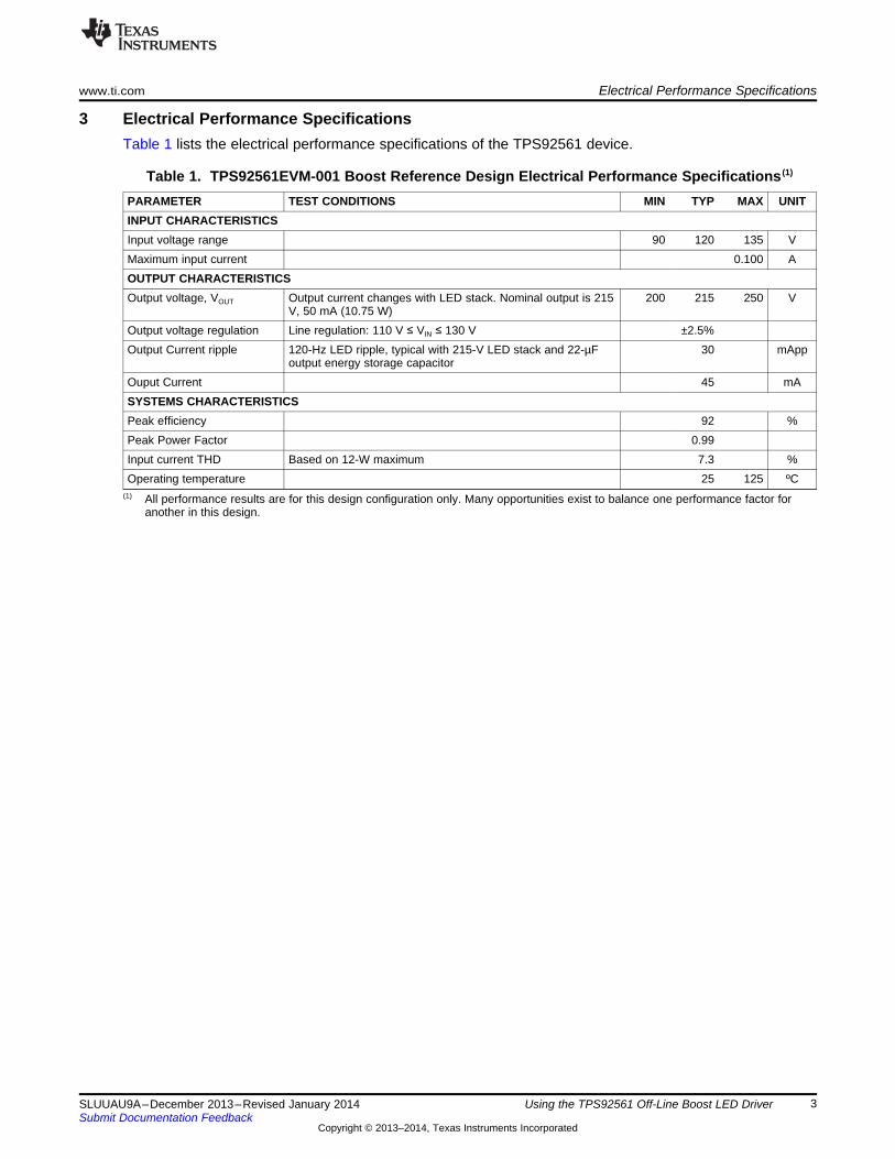
3 Electrical Performance SpecificationsTable 1 lists the electrical performance specifications of the TPS92561 device.
Table 1. TPS92561EVM-001 Boost Reference Design Electrical Performance Specifications (1)
PARAMETER TEST CONDITIONS MIN TYP MAX UNITINPUT CHARACTERISTICSInput voltage range 90 120 135 VMaximum input current 0.100 AOUTPUT CHARACTERISTICSOutput voltage, VOUT Output current changes with LED stack. Nominal output is 215 200 215 250 V
V, 50 mA (10.75 W)Output voltage regulation Line regulation: 110 V ≤ VIN ≤ 130 V ±2.5%Output Current ripple 120-Hz LED ripple, typical with 215-V LED stack and 22-µF 30 mApp
output energy storage capacitorOuput Current 45 mASYSTEMS CHARACTERISTICSPeak efficiency 92 %Peak Power Factor 0.99Input current THD Based on 12-W maximum 7.3 %Operating temperature 25 125 ºC
(1) All performance results are for this design configuration only. Many opportunities exist to balance one performance factor foranother in this design.
3SLUUAU9A–December 2013–Revised January 2014 Using the TPS92561 Off-Line Boost LED DriverSubmit Documentation Feedback
Copyright © 2013–2014, Texas Instruments Incorporated
Schematic www.ti.com
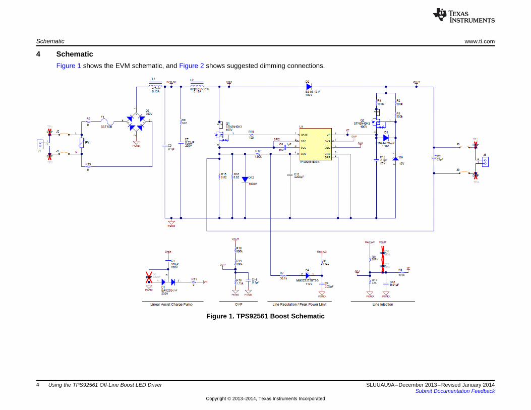
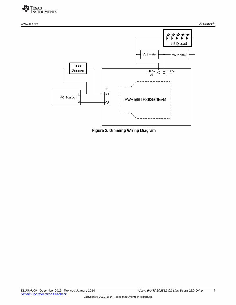
4 SchematicFigure 1 shows the EVM schematic, and Figure 2 shows suggested dimming connections.
Figure 1. TPS92561 Boost Schematic
4 Using the TPS92561 Off-Line Boost LED Driver SLUUAU9A–December 2013–Revised January 2014Submit Documentation Feedback
Copyright © 2013–2014, Texas Instruments Incorporated
J1
AC SourceL
N
Triac Dimmer
PWR588TPS92561EVM
J5LED+
AMP Meter
L E D Load
LED-
Volt Meter
www.ti.com Schematic
Figure 2. Dimming Wiring Diagram
5SLUUAU9A–December 2013–Revised January 2014 Using the TPS92561 Off-Line Boost LED DriverSubmit Documentation Feedback
Copyright © 2013–2014, Texas Instruments Incorporated
0.7000
0.7500
0.8000
0.8500
0.9000
0.9500
1.0000
1.0500
1.1000
85 90 95 100 105 110 115 120 125 130 135 140
Pow
er F
acto
r
Input Voltage (VRMS)
C002
85
86
87
88
89
90
91
92
93
94
95
85 90 95 100 105 110 115 120 125 130 135 140
Effi
cien
cy (
%)
Input Voltage (VRMS)
C001
Performance Data and Typical Characteristic Curves www.ti.com
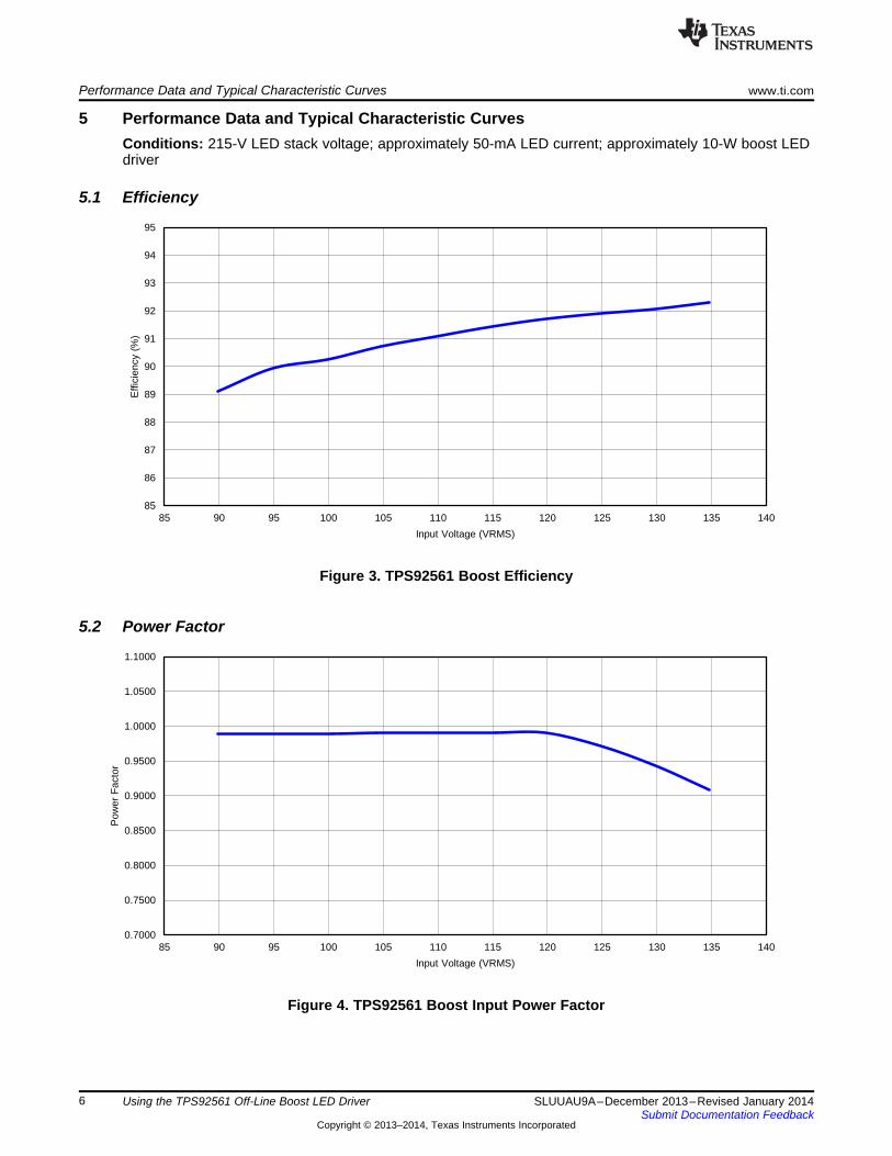
5 Performance Data and Typical Characteristic CurvesConditions: 215-V LED stack voltage; approximately 50-mA LED current; approximately 10-W boost LEDdriver
5.1 Efficiency
Figure 3. TPS92561 Boost Efficiency
5.2 Power Factor
Figure 4. TPS92561 Boost Input Power Factor
6 Using the TPS92561 Off-Line Boost LED Driver SLUUAU9A–December 2013–Revised January 2014Submit Documentation Feedback
Copyright © 2013–2014, Texas Instruments Incorporated
Ch3
Ch4
Ch1&2
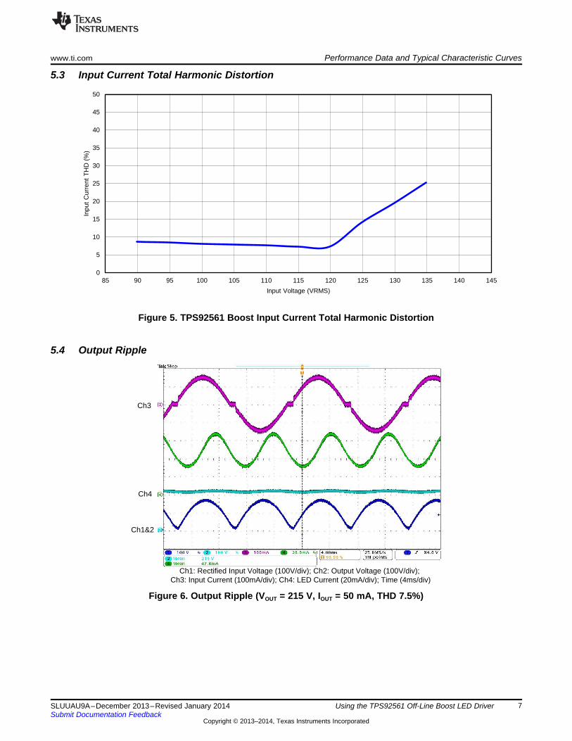
Ch1: Rectified Input Voltage (100V/div); Ch2: Output Voltage (100V/div); Ch3: Input Current (100mA/div); Ch4: LED Current (20mA/div); Time (4ms/div)
0
5
10
15
20
25
30
35
40
45
50
85 90 95 100 105 110 115 120 125 130 135 140 145
Inpu
t C
urre
nt T
HD
(%
)
Input Voltage (VRMS)
C003
www.ti.com Performance Data and Typical Characteristic Curves
5.3 Input Current Total Harmonic Distortion
Figure 5. TPS92561 Boost Input Current Total Harmonic Distortion
5.4 Output Ripple
Figure 6. Output Ripple (VOUT = 215 V, IOUT = 50 mA, THD 7.5%)
7SLUUAU9A–December 2013–Revised January 2014 Using the TPS92561 Off-Line Boost LED DriverSubmit Documentation Feedback
Copyright © 2013–2014, Texas Instruments Incorporated
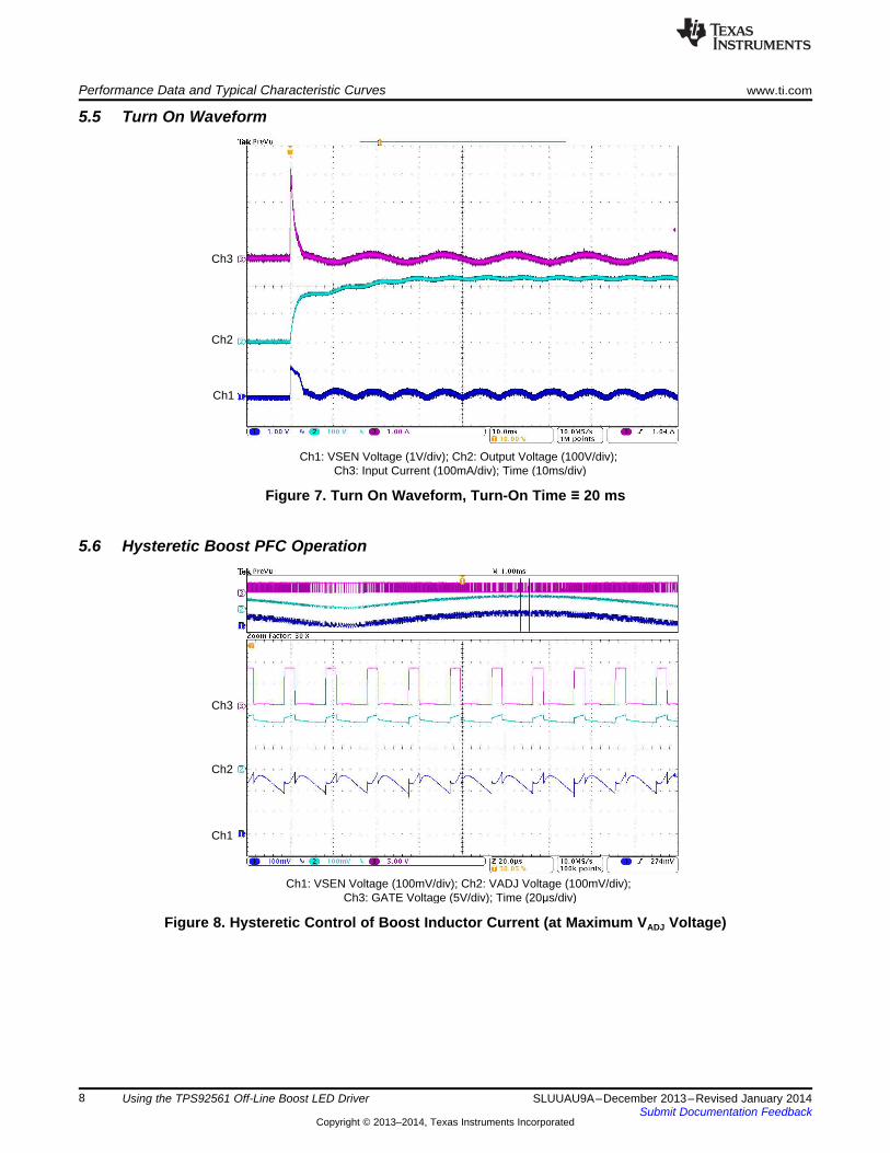
Ch1: VSEN Voltage (100mV/div); Ch2: VADJ Voltage (100mV/div); Ch3: GATE Voltage (5V/div); Time (20�s/div)
Ch3
Ch2
Ch1
Ch1: VSEN Voltage (1V/div); Ch2: Output Voltage (100V/div); Ch3: Input Current (100mA/div); Time (10ms/div)
Ch3
Ch2
Ch1
Performance Data and Typical Characteristic Curves www.ti.com
5.5 Turn On Waveform
Figure 7. Turn On Waveform, Turn-On Time ≡ 20 ms
5.6 Hysteretic Boost PFC Operation
Figure 8. Hysteretic Control of Boost Inductor Current (at Maximum VADJ Voltage)
8 Using the TPS92561 Off-Line Boost LED Driver SLUUAU9A–December 2013–Revised January 2014Submit Documentation Feedback
Copyright © 2013–2014, Texas Instruments Incorporated
Ch1: Rectified Input Voltage (50V/div); Ch3: Input Current (100mA/div); Time (4ms/div)
Ch3
Ch1
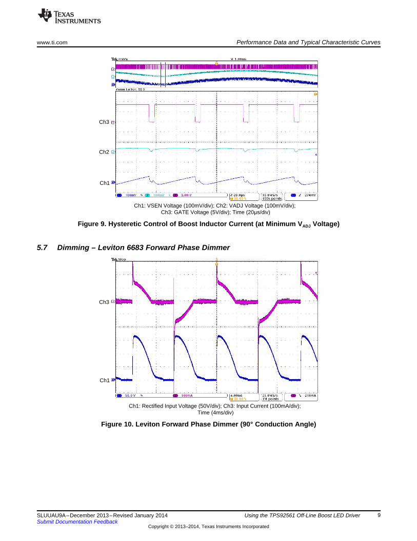
Ch1: VSEN Voltage (100mV/div); Ch2: VADJ Voltage (100mV/div); Ch3: GATE Voltage (5V/div); Time (20�s/div)
Ch3
Ch2
Ch1
www.ti.com Performance Data and Typical Characteristic Curves
Figure 9. Hysteretic Control of Boost Inductor Current (at Minimum VADJ Voltage)
5.7 Dimming – Leviton 6683 Forward Phase Dimmer
Figure 10. Leviton Forward Phase Dimmer (90° Conduction Angle)
9SLUUAU9A–December 2013–Revised January 2014 Using the TPS92561 Off-Line Boost LED DriverSubmit Documentation Feedback
Copyright © 2013–2014, Texas Instruments Incorporated
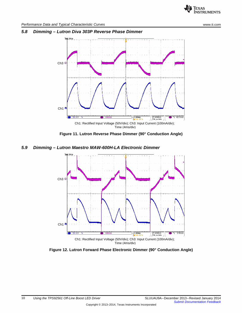
Ch1: Rectified Input Voltage (50V/div); Ch3: Input Current (100mA/div); Time (4ms/div)
Ch3
Ch1
Ch1: Rectified Input Voltage (50V/div); Ch3: Input Current (100mA/div); Time (4ms/div)
Ch3
Ch1
Performance Data and Typical Characteristic Curves www.ti.com
5.8 Dimming – Lutron Diva 303P Reverse Phase Dimmer
Figure 11. Lutron Reverse Phase Dimmer (90° Conduction Angle)
5.9 Dimming – Lutron Maestro MAW-600H-LA Electronic Dimmer
Figure 12. Lutron Forward Phase Electronic Dimmer (90° Conduction Angle)
10 Using the TPS92561 Off-Line Boost LED Driver SLUUAU9A–December 2013–Revised January 2014Submit Documentation Feedback
Copyright © 2013–2014, Texas Instruments Incorporated
0
10
20
30
40
50
60
70
80
90
100
110
0 10 20 30 40 50 60 70 80 90 100 110 120 130
Nor
mal
ized
LE
D C
urre
nt (
%)
Input Voltage with series dimmer connection (VRMS)
NEMA Upper Limit
NEMA Lower Limit
Forward Phase
Reverse Phase
Electronic Dimmer
C004
www.ti.com Performance Data and Typical Characteristic Curves
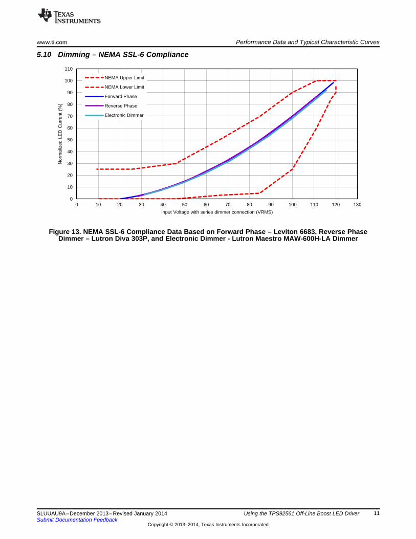
5.10 Dimming – NEMA SSL-6 Compliance
Figure 13. NEMA SSL-6 Compliance Data Based on Forward Phase – Leviton 6683, Reverse PhaseDimmer – Lutron Diva 303P, and Electronic Dimmer - Lutron Maestro MAW-600H-LA Dimmer
11SLUUAU9A–December 2013–Revised January 2014 Using the TPS92561 Off-Line Boost LED DriverSubmit Documentation Feedback
Copyright © 2013–2014, Texas Instruments Incorporated
Performance Data and Typical Characteristic Curves www.ti.com
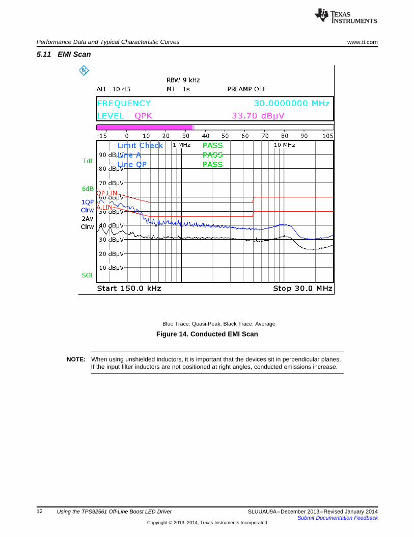
5.11 EMI Scan
spacerspacerspacerspacerspacerspacerBlue Trace: Quasi-Peak, Black Trace: Average
Figure 14. Conducted EMI Scan
NOTE: When using unshielded inductors, it is important that the devices sit in perpendicular planes.If the input filter inductors are not positioned at right angles, conducted emissions increase.
12 Using the TPS92561 Off-Line Boost LED Driver SLUUAU9A–December 2013–Revised January 2014Submit Documentation Feedback
Copyright © 2013–2014, Texas Instruments Incorporated
www.ti.com Performance Data and Typical Characteristic Curves
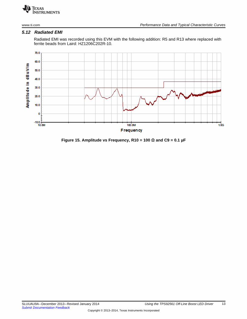
5.12 Radiated EMIRadiated EMI was recorded using this EVM with the following addition: R5 and R13 where replaced withferrite beads from Laird: HZ1206C202R-10.
Figure 15. Amplitude vs Frequency, R10 = 100 Ω and C9 = 0.1 µF
13SLUUAU9A–December 2013–Revised January 2014 Using the TPS92561 Off-Line Boost LED DriverSubmit Documentation Feedback
Copyright © 2013–2014, Texas Instruments Incorporated
Performance Data and Typical Characteristic Curves www.ti.com
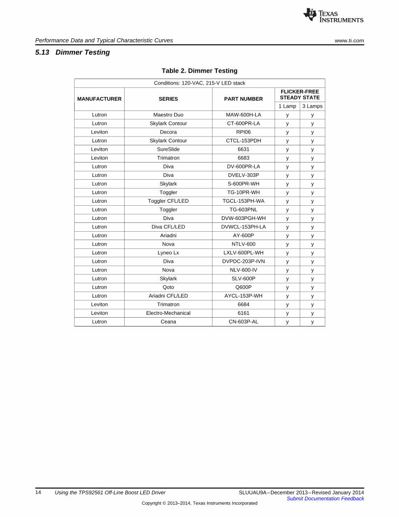
5.13 Dimmer Testing
Table 2. Dimmer Testing
Conditions: 120-VAC, 215-V LED stackFLICKER-FREESTEADY STATEMANUFACTURER SERIES PART NUMBER1 Lamp 3 Lamps
Lutron Maestro Duo MAW-600H-LA y yLutron Skylark Contour CT-600PR-LA y yLeviton Decora RPI06 y yLutron Skylark Contour CTCL-153PDH y yLeviton SureSlide 6631 y yLeviton Trimatron 6683 y yLutron Diva DV-600PR-LA y yLutron Diva DVELV-303P y yLutron Skylark S-600PR-WH y yLutron Toggler TG-10PR-WH y yLutron Toggler CFL/LED TGCL-153PH-WA y yLutron Toggler TG-603PNL y yLutron Diva DVW-603PGH-WH y yLutron Diva CFL/LED DVWCL-153PH-LA y yLutron Ariadni AY-600P y yLutron Nova NTLV-600 y yLutron Lyneo Lx LXLV-600PL-WH y yLutron Diva DVPDC-203P-IVN y yLutron Nova NLV-600-IV y yLutron Skylark SLV-600P y yLutron Qoto Q600P y yLutron Ariadni CFL/LED AYCL-153P-WH y yLeviton Trimatron 6684 y yLeviton Electro-Mechanical 6161 y yLutron Ceana CN-603P-AL y y
14 Using the TPS92561 Off-Line Boost LED Driver SLUUAU9A–December 2013–Revised January 2014Submit Documentation Feedback
Copyright © 2013–2014, Texas Instruments Incorporated
www.ti.com Reference Design, Assembly Drawing, PCB Layout, and Bill of Materials
6 Reference Design, Assembly Drawing, PCB Layout, and Bill of Materials
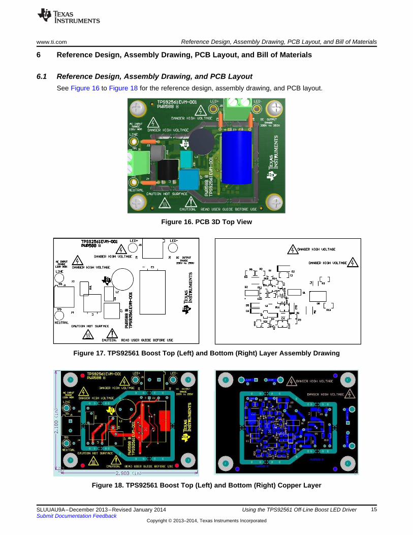
6.1 Reference Design, Assembly Drawing, and PCB LayoutSee Figure 16 to Figure 18 for the reference design, assembly drawing, and PCB layout.
Figure 16. PCB 3D Top View
Figure 17. TPS92561 Boost Top (Left) and Bottom (Right) Layer Assembly Drawing
Figure 18. TPS92561 Boost Top (Left) and Bottom (Right) Copper Layer
15SLUUAU9A–December 2013–Revised January 2014 Using the TPS92561 Off-Line Boost LED DriverSubmit Documentation Feedback
Copyright © 2013–2014, Texas Instruments Incorporated
Reference Design, Assembly Drawing, PCB Layout, and Bill of Materials www.ti.com
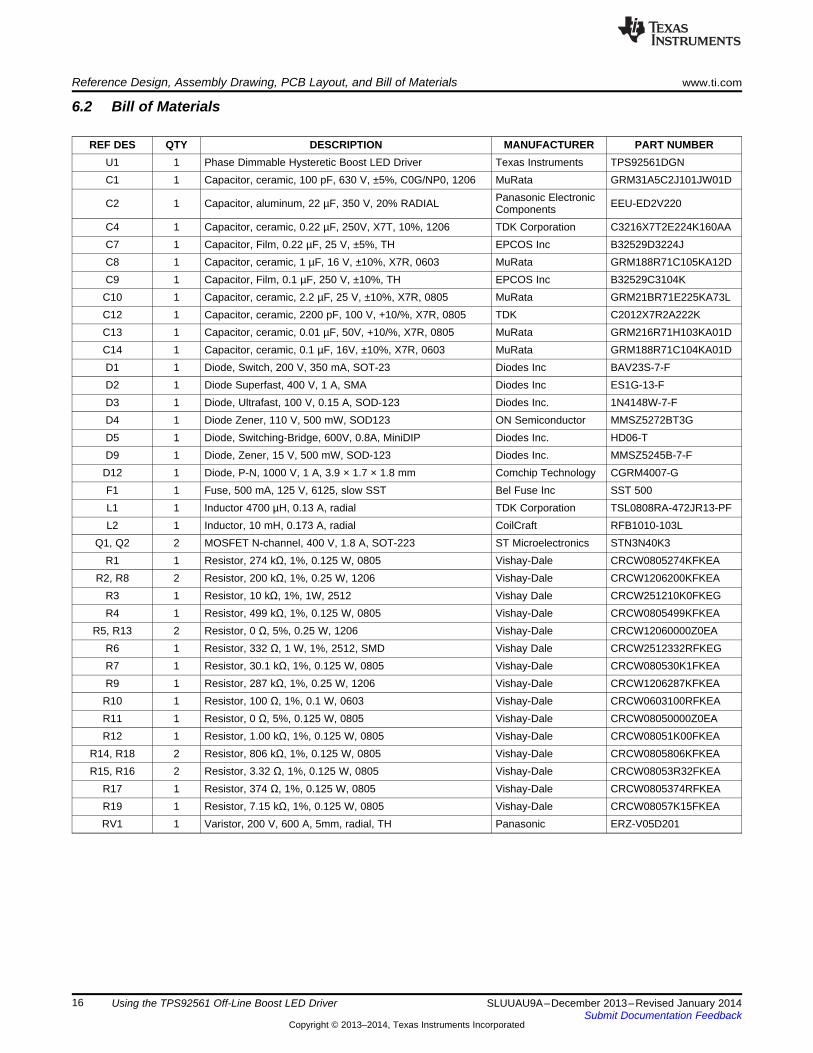
6.2 Bill of Materials
REF DES QTY DESCRIPTION MANUFACTURER PART NUMBERU1 1 Phase Dimmable Hysteretic Boost LED Driver Texas Instruments TPS92561DGNC1 1 Capacitor, ceramic, 100 pF, 630 V, ±5%, C0G/NP0, 1206 MuRata GRM31A5C2J101JW01D
Panasonic ElectronicC2 1 Capacitor, aluminum, 22 µF, 350 V, 20% RADIAL EEU-ED2V220ComponentsC4 1 Capacitor, ceramic, 0.22 µF, 250V, X7T, 10%, 1206 TDK Corporation C3216X7T2E224K160AAC7 1 Capacitor, Film, 0.22 µF, 25 V, ±5%, TH EPCOS Inc B32529D3224JC8 1 Capacitor, ceramic, 1 µF, 16 V, ±10%, X7R, 0603 MuRata GRM188R71C105KA12DC9 1 Capacitor, Film, 0.1 µF, 250 V, ±10%, TH EPCOS Inc B32529C3104KC10 1 Capacitor, ceramic, 2.2 µF, 25 V, ±10%, X7R, 0805 MuRata GRM21BR71E225KA73LC12 1 Capacitor, ceramic, 2200 pF, 100 V, +10/%, X7R, 0805 TDK C2012X7R2A222KC13 1 Capacitor, ceramic, 0.01 µF, 50V, +10/%, X7R, 0805 MuRata GRM216R71H103KA01DC14 1 Capacitor, ceramic, 0.1 µF, 16V, ±10%, X7R, 0603 MuRata GRM188R71C104KA01DD1 1 Diode, Switch, 200 V, 350 mA, SOT-23 Diodes Inc BAV23S-7-FD2 1 Diode Superfast, 400 V, 1 A, SMA Diodes Inc ES1G-13-FD3 1 Diode, Ultrafast, 100 V, 0.15 A, SOD-123 Diodes Inc. 1N4148W-7-FD4 1 Diode Zener, 110 V, 500 mW, SOD123 ON Semiconductor MMSZ5272BT3GD5 1 Diode, Switching-Bridge, 600V, 0.8A, MiniDIP Diodes Inc. HD06-TD9 1 Diode, Zener, 15 V, 500 mW, SOD-123 Diodes Inc. MMSZ5245B-7-FD12 1 Diode, P-N, 1000 V, 1 A, 3.9 × 1.7 × 1.8 mm Comchip Technology CGRM4007-GF1 1 Fuse, 500 mA, 125 V, 6125, slow SST Bel Fuse Inc SST 500L1 1 Inductor 4700 µH, 0.13 A, radial TDK Corporation TSL0808RA-472JR13-PFL2 1 Inductor, 10 mH, 0.173 A, radial CoilCraft RFB1010-103L
Q1, Q2 2 MOSFET N-channel, 400 V, 1.8 A, SOT-223 ST Microelectronics STN3N40K3R1 1 Resistor, 274 kΩ, 1%, 0.125 W, 0805 Vishay-Dale CRCW0805274KFKEA
R2, R8 2 Resistor, 200 kΩ, 1%, 0.25 W, 1206 Vishay-Dale CRCW1206200KFKEAR3 1 Resistor, 10 kΩ, 1%, 1W, 2512 Vishay Dale CRCW251210K0FKEGR4 1 Resistor, 499 kΩ, 1%, 0.125 W, 0805 Vishay-Dale CRCW0805499KFKEA
R5, R13 2 Resistor, 0 Ω, 5%, 0.25 W, 1206 Vishay-Dale CRCW12060000Z0EAR6 1 Resistor, 332 Ω, 1 W, 1%, 2512, SMD Vishay Dale CRCW2512332RFKEGR7 1 Resistor, 30.1 kΩ, 1%, 0.125 W, 0805 Vishay-Dale CRCW080530K1FKEAR9 1 Resistor, 287 kΩ, 1%, 0.25 W, 1206 Vishay-Dale CRCW1206287KFKEAR10 1 Resistor, 100 Ω, 1%, 0.1 W, 0603 Vishay-Dale CRCW0603100RFKEAR11 1 Resistor, 0 Ω, 5%, 0.125 W, 0805 Vishay-Dale CRCW08050000Z0EAR12 1 Resistor, 1.00 kΩ, 1%, 0.125 W, 0805 Vishay-Dale CRCW08051K00FKEA
R14, R18 2 Resistor, 806 kΩ, 1%, 0.125 W, 0805 Vishay-Dale CRCW0805806KFKEAR15, R16 2 Resistor, 3.32 Ω, 1%, 0.125 W, 0805 Vishay-Dale CRCW08053R32FKEA
R17 1 Resistor, 374 Ω, 1%, 0.125 W, 0805 Vishay-Dale CRCW0805374RFKEAR19 1 Resistor, 7.15 kΩ, 1%, 0.125 W, 0805 Vishay-Dale CRCW08057K15FKEARV1 1 Varistor, 200 V, 600 A, 5mm, radial, TH Panasonic ERZ-V05D201
16 Using the TPS92561 Off-Line Boost LED Driver SLUUAU9A–December 2013–Revised January 2014Submit Documentation Feedback
Copyright © 2013–2014, Texas Instruments Incorporated
www.ti.com Reference Design, Assembly Drawing, PCB Layout, and Bill of Materials
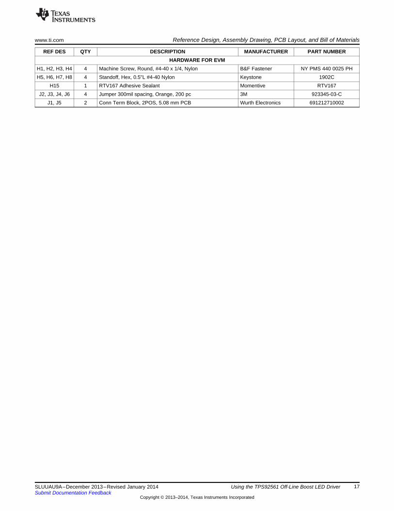
REF DES QTY DESCRIPTION MANUFACTURER PART NUMBERHARDWARE FOR EVM
H1, H2, H3, H4 4 Machine Screw, Round, #4-40 x 1/4, Nylon B&F Fastener NY PMS 440 0025 PHH5, H6, H7, H8 4 Standoff, Hex, 0.5"L #4-40 Nylon Keystone 1902C
H15 1 RTV167 Adhesive Sealant Momentive RTV167J2, J3, J4, J6 4 Jumper 300mil spacing, Orange, 200 pc 3M 923345-03-C
J1, J5 2 Conn Term Block, 2POS, 5.08 mm PCB Wurth Electronics 691212710002
17SLUUAU9A–December 2013–Revised January 2014 Using the TPS92561 Off-Line Boost LED DriverSubmit Documentation Feedback
Copyright © 2013–2014, Texas Instruments Incorporated
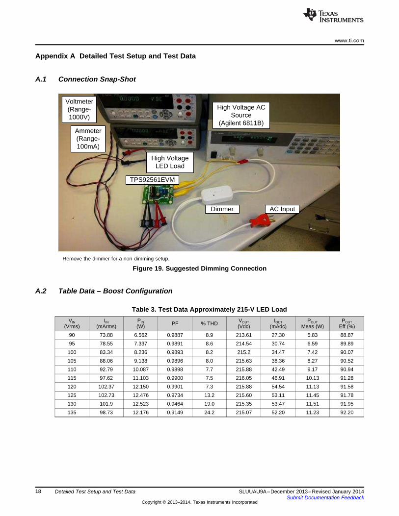
High Voltage LED Load
Dimmer AC Input
High Voltage AC Source
(Agilent 6811B)
Voltmeter (Range-1000V)
Ammeter (Range-100mA)
TPS92561EVM
www.ti.com
Appendix A Detailed Test Setup and Test Data
A.1 Connection Snap-Shot
Remove the dimmer for a non-dimming setup.
Figure 19. Suggested Dimming Connection
A.2 Table Data – Boost Configuration
Table 3. Test Data Approximately 215-V LED LoadVIN IIN PIN VOUT IOUT POUT POUTPF % THD(Vrms) (mArms) (W) (Vdc) (mAdc) Meas (W) Eff (%)90 73.88 6.562 0.9887 8.9 213.61 27.30 5.83 88.8795 78.55 7.337 0.9891 8.6 214.54 30.74 6.59 89.89100 83.34 8.236 0.9893 8.2 215.2 34.47 7.42 90.07105 88.06 9.138 0.9896 8.0 215.63 38.36 8.27 90.52110 92.79 10.087 0.9898 7.7 215.88 42.49 9.17 90.94115 97.62 11.103 0.9900 7.5 216.05 46.91 10.13 91.28120 102.37 12.150 0.9901 7.3 215.88 54.54 11.13 91.58125 102.73 12.476 0.9734 13.2 215.60 53.11 11.45 91.78130 101.9 12.523 0.9464 19.0 215.35 53.47 11.51 91.95135 98.73 12.176 0.9149 24.2 215.07 52.20 11.23 92.20
18 Detailed Test Setup and Test Data SLUUAU9A–December 2013–Revised January 2014Submit Documentation Feedback
Copyright © 2013–2014, Texas Instruments Incorporated
www.ti.com Table Data – Boost Configuration
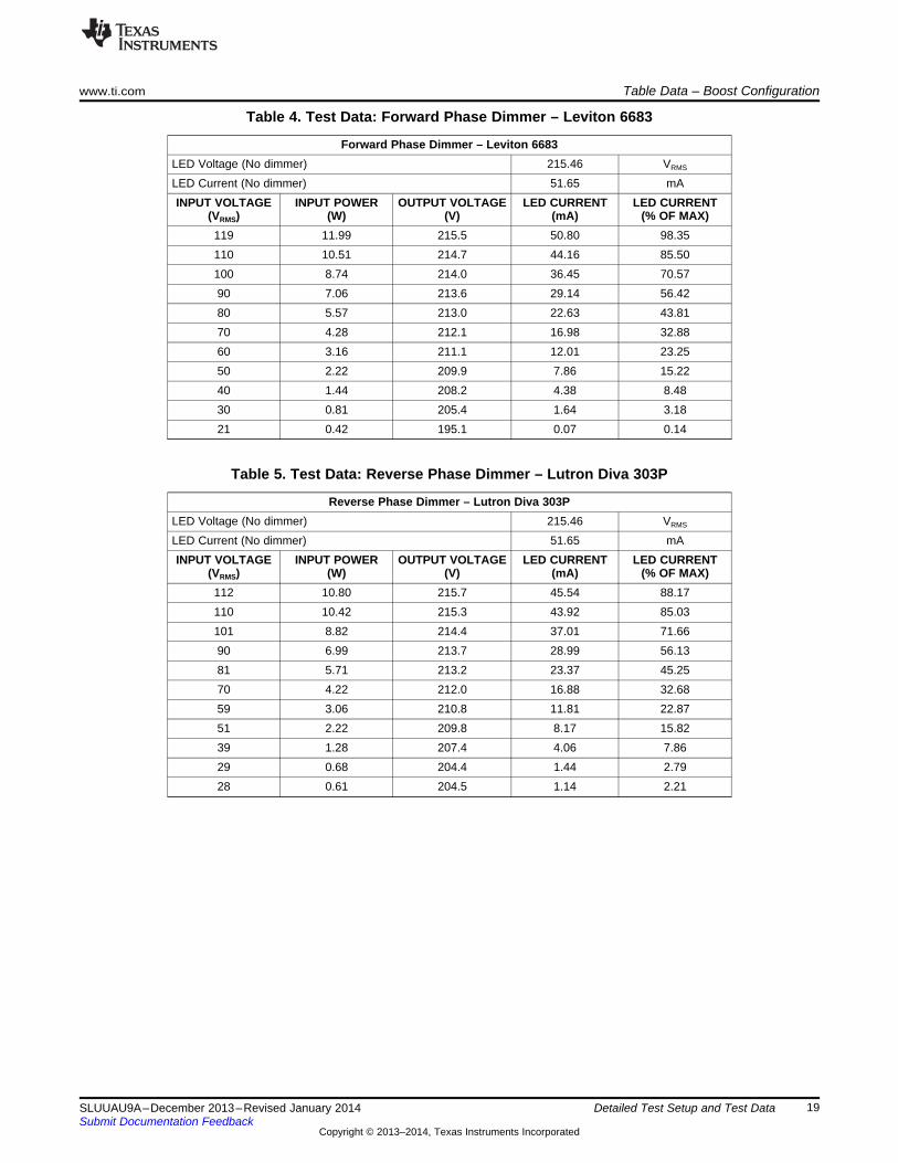
Table 4. Test Data: Forward Phase Dimmer – Leviton 6683
Forward Phase Dimmer – Leviton 6683LED Voltage (No dimmer) 215.46 VRMS
LED Current (No dimmer) 51.65 mAINPUT VOLTAGE INPUT POWER OUTPUT VOLTAGE LED CURRENT LED CURRENT
(VRMS) (W) (V) (mA) (% OF MAX)119 11.99 215.5 50.80 98.35110 10.51 214.7 44.16 85.50100 8.74 214.0 36.45 70.5790 7.06 213.6 29.14 56.4280 5.57 213.0 22.63 43.8170 4.28 212.1 16.98 32.8860 3.16 211.1 12.01 23.2550 2.22 209.9 7.86 15.2240 1.44 208.2 4.38 8.4830 0.81 205.4 1.64 3.1821 0.42 195.1 0.07 0.14
Table 5. Test Data: Reverse Phase Dimmer – Lutron Diva 303P
Reverse Phase Dimmer – Lutron Diva 303PLED Voltage (No dimmer) 215.46 VRMS
LED Current (No dimmer) 51.65 mAINPUT VOLTAGE INPUT POWER OUTPUT VOLTAGE LED CURRENT LED CURRENT
(VRMS) (W) (V) (mA) (% OF MAX)112 10.80 215.7 45.54 88.17110 10.42 215.3 43.92 85.03101 8.82 214.4 37.01 71.6690 6.99 213.7 28.99 56.1381 5.71 213.2 23.37 45.2570 4.22 212.0 16.88 32.6859 3.06 210.8 11.81 22.8751 2.22 209.8 8.17 15.8239 1.28 207.4 4.06 7.8629 0.68 204.4 1.44 2.7928 0.61 204.5 1.14 2.21
19SLUUAU9A–December 2013–Revised January 2014 Detailed Test Setup and Test DataSubmit Documentation Feedback
Copyright © 2013–2014, Texas Instruments Incorporated
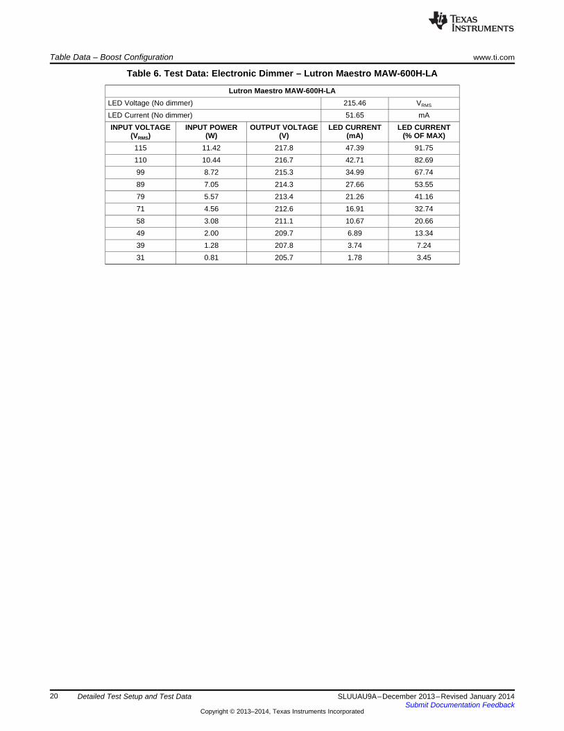
Table Data – Boost Configuration www.ti.com
Table 6. Test Data: Electronic Dimmer – Lutron Maestro MAW-600H-LA
Lutron Maestro MAW-600H-LALED Voltage (No dimmer) 215.46 VRMS
LED Current (No dimmer) 51.65 mAINPUT VOLTAGE INPUT POWER OUTPUT VOLTAGE LED CURRENT LED CURRENT
(VRMS) (W) (V) (mA) (% OF MAX)115 11.42 217.8 47.39 91.75110 10.44 216.7 42.71 82.6999 8.72 215.3 34.99 67.7489 7.05 214.3 27.66 53.5579 5.57 213.4 21.26 41.1671 4.56 212.6 16.91 32.7458 3.08 211.1 10.67 20.6649 2.00 209.7 6.89 13.3439 1.28 207.8 3.74 7.2431 0.81 205.7 1.78 3.45
20 Detailed Test Setup and Test Data SLUUAU9A–December 2013–Revised January 2014Submit Documentation Feedback
Copyright © 2013–2014, Texas Instruments Incorporated
VP
OVP
ADJ
GATE
SRC
VCC
TPS92561
GNDSEN
L
VP
OVP
ADJ
GATE
SRC
VCC
TPS92561
GNDSEN
1
2
L
www.ti.com
Appendix B Layout Considerations
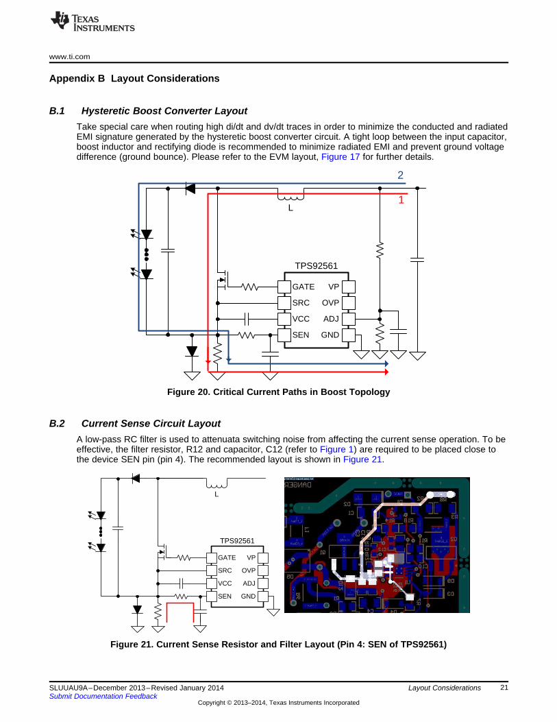
B.1 Hysteretic Boost Converter LayoutTake special care when routing high di/dt and dv/dt traces in order to minimize the conducted and radiatedEMI signature generated by the hysteretic boost converter circuit. A tight loop between the input capacitor,boost inductor and rectifying diode is recommended to minimize radiated EMI and prevent ground voltagedifference (ground bounce). Please refer to the EVM layout, Figure 17 for further details.
Figure 20. Critical Current Paths in Boost Topology
B.2 Current Sense Circuit LayoutA low-pass RC filter is used to attenuata switching noise from affecting the current sense operation. To beeffective, the filter resistor, R12 and capacitor, C12 (refer to Figure 1) are required to be placed close tothe device SEN pin (pin 4). The recommended layout is shown in Figure 21.
Figure 21. Current Sense Resistor and Filter Layout (Pin 4: SEN of TPS92561)
21SLUUAU9A–December 2013–Revised January 2014 Layout ConsiderationsSubmit Documentation Feedback
Copyright © 2013–2014, Texas Instruments Incorporated
VP
OVP
ADJ
GATE
SRC
VCC
TPS92561
GNDSEN
L
Gate-Drive Output and Switching MOSFET Layout www.ti.com
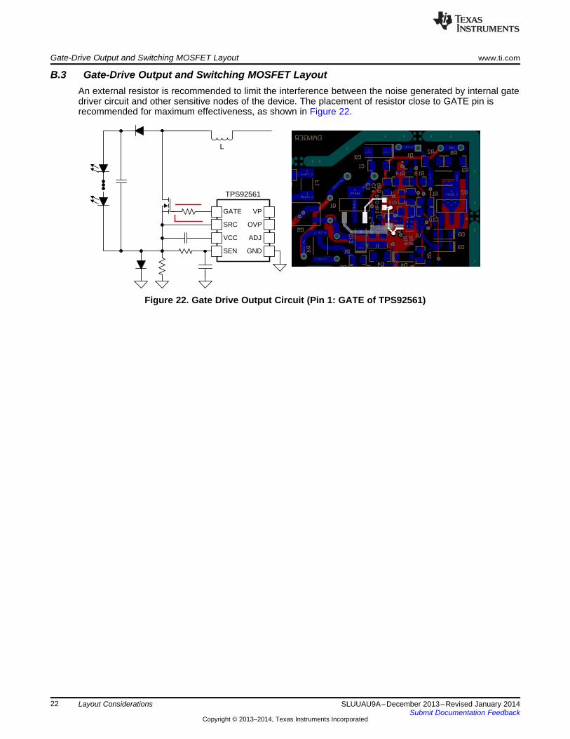
B.3 Gate-Drive Output and Switching MOSFET LayoutAn external resistor is recommended to limit the interference between the noise generated by internal gatedriver circuit and other sensitive nodes of the device. The placement of resistor close to GATE pin isrecommended for maximum effectiveness, as shown in Figure 22.
Figure 22. Gate Drive Output Circuit (Pin 1: GATE of TPS92561)
22 Layout Considerations SLUUAU9A–December 2013–Revised January 2014Submit Documentation Feedback
Copyright © 2013–2014, Texas Instruments Incorporated

� �sw
LED sw
1 mA + Qg fC1 =
V f
u
u
LED swC V fu u
www.ti.com
Appendix C EVM Circuit Options Used
C.1 Charge Pump Linear AssistThe TPS92561 data sheet describes methods to provide power to the IC. The method selected for thisEVM uses the 'Linear regulator from output' method, deriving the IC bias voltage from the converteroutput. This causes a larger loss in the linear circuitry but provides performance advantages including: amore consistent turn off and a VP voltage with less variation when dimming. To gain some of theefficiency loss back, a charge pump is used (C1 and D1), as shown in Figure 1 , to assist the main linearregulator (Q2, D9, R2, R3, R8) by transferring charge to the bias circuit using a method that incurs lowerlosses than if it were derived from the linear regulator directly.
If the value of C1 is too high, the increase in associated switching losses in Q1 will not offset the gainsmade by reducing the current draw through the linear. An optimal operation point is reached when thevoltage provided by the charge pump is just slightly higher then the voltage generated by the linearcircuitry. As a good starting point to selecting the C1 value, we consider the current capability of thecapacitance circuit and the current requirements of the IC. The IC uses approximately 1 mA plus theadditional current required to switch the main FET (Qg × fsw). The C1 capacitor can provide a currentbased on the capacitance value, the voltage across the capacitor and the frequency of operation:
(1)
By combining the terms and solving for C1 we obtain:
(2)
After a capacitance value is obtained, some fine tuning under typical operating conditions should beconsidered as several factors affect the circuit performance including: exact LED voltage, VP bias voltage(Zener voltage and FET VGS voltage), main FET gate charge requirements, and the variability of theconverter switching frequency. In general the addition of the charge pump circuit can increase theconverter efficiency 1% to 2% when compared to the linear from the output voltage alone. The highestpossible efficiency is still achieved if an auxiliary winding is used to generate the bias voltage.
23SLUUAU9A–December 2013–Revised January 2014 EVM Circuit Options UsedSubmit Documentation Feedback
Copyright © 2013–2014, Texas Instruments Incorporated
Vout IoutVin Iin =
nu
u
� �V_high_line 0.9 VzR_total = 586 k
V _ ADJ R12
u � :
' y
10.8 R17V_ADJ = 140 mV
R9 R17u
' |�
� �VrectAC 132 120 2 .638 10.8 V' � u u
Line Regulation and Peak Power Limit www.ti.com
C.2 Line Regulation and Peak Power LimitThe EVM reference (ADJ pin voltage) is generated by dividing down the rectified AC voltage. This is avery simple method of generating the converter reference, but it also means the reference will change ifthe line voltage changes. When considering an LED bulb design for the US or Canadian market, long-termoperation at input voltages that vary greatly from the nominal are not always considered. A simple meansto ensure the LED heat sink temperature will remain controlled is to add this power limiting/line regulationcircuit (R1, R7, D4, C4).
We can first estimate the voltage change at the ADJ pin (our reference voltage) based on the line changeand consider an example for a line change from 120 to 132 VAC.
(3)
Equation 3 gives us the average change in the average rectified AC voltage of approximately 10.8 V. Wecan apply this to our divider based on R9 and R17:
(4)
The Zener was selected as 110 V based on the average rectified AC voltage for 120 VAC of 108 V.
Next we can design our compensation circuit to apply that same voltage offset when the average rectifiedAC voltage increases. Based on the circuit designators R1, D4, R7, R12 and the combination of R15 andR16 we can solve for the series resistance required to provide the current required to apply an offsetvoltage equal to the amount change due to the line. A simplified expression can be used:
(5)
Equation 5 represents the total resistance of R1 + R7. The resistance should be split with a heavy bias toR1 limiting the voltage ripple on C4. After the circuit is in place, a few tests should be completed to allowfine tuning of the resistance values. This simplified approach did not account for the smaller variation fromthe conversion itself (given that the converter is controlling the input current, not the output current by therelationship:
(6)
24 EVM Circuit Options Used SLUUAU9A–December 2013–Revised January 2014Submit Documentation Feedback
Copyright © 2013–2014, Texas Instruments Incorporated
www.ti.com Revision History
Revision History
Changes from Original (December 2013) to A Revision ................................................................................................ Page
• Added a graph for Radiated EMI section ............................................................................................ 13• Added link to Figure 1 reference ...................................................................................................... 23• Added Appendix C for EVM Circuit Options Used .................................................................................. 23
NOTE: Page numbers for previous revisions may differ from page numbers in the current version.
25SLUUAU9A–December 2013–Revised January 2014 Revision HistorySubmit Documentation Feedback
Copyright © 2013–2014, Texas Instruments Incorporated

EVALUATION BOARD/KIT/MODULE (EVM) ADDITIONAL TERMSTexas Instruments (TI) provides the enclosed Evaluation Board/Kit/Module (EVM) under the following conditions:The user assumes all responsibility and liability for proper and safe handling of the goods. Further, the user indemnifies TI from all claimsarising from the handling or use of the goods.Should this evaluation board/kit not meet the specifications indicated in the User’s Guide, the board/kit may be returned within 30 days fromthe date of delivery for a full refund. THE FOREGOING LIMITED WARRANTY IS THE EXCLUSIVE WARRANTY MADE BY SELLER TOBUYER AND IS IN LIEU OF ALL OTHER WARRANTIES, EXPRESSED, IMPLIED, OR STATUTORY, INCLUDING ANY WARRANTY OFMERCHANTABILITY OR FITNESS FOR ANY PARTICULAR PURPOSE. EXCEPT TO THE EXTENT OF THE INDEMNITY SET FORTHABOVE, NEITHER PARTY SHALL BE LIABLE TO THE OTHER FOR ANY INDIRECT, SPECIAL, INCIDENTAL, OR CONSEQUENTIALDAMAGES.Please read the User's Guide and, specifically, the Warnings and Restrictions notice in the User's Guide prior to handling the product. Thisnotice contains important safety information about temperatures and voltages. For additional information on TI's environmental and/or safetyprograms, please visit www.ti.com/esh or contact TI.No license is granted under any patent right or other intellectual property right of TI covering or relating to any machine, process, orcombination in which such TI products or services might be or are used. TI currently deals with a variety of customers for products, andtherefore our arrangement with the user is not exclusive. TI assumes no liability for applications assistance, customer product design,software performance, or infringement of patents or services described herein.
REGULATORY COMPLIANCE INFORMATIONAs noted in the EVM User’s Guide and/or EVM itself, this EVM and/or accompanying hardware may or may not be subject to the FederalCommunications Commission (FCC) and Industry Canada (IC) rules.For EVMs not subject to the above rules, this evaluation board/kit/module is intended for use for ENGINEERING DEVELOPMENT,DEMONSTRATION OR EVALUATION PURPOSES ONLY and is not considered by TI to be a finished end product fit for general consumeruse. It generates, uses, and can radiate radio frequency energy and has not been tested for compliance with the limits of computingdevices pursuant to part 15 of FCC or ICES-003 rules, which are designed to provide reasonable protection against radio frequencyinterference. Operation of the equipment may cause interference with radio communications, in which case the user at his own expense willbe required to take whatever measures may be required to correct this interference.General Statement for EVMs including a radioUser Power/Frequency Use Obligations: This radio is intended for development/professional use only in legally allocated frequency andpower limits. Any use of radio frequencies and/or power availability of this EVM and its development application(s) must comply with locallaws governing radio spectrum allocation and power limits for this evaluation module. It is the user’s sole responsibility to only operate thisradio in legally acceptable frequency space and within legally mandated power limitations. Any exceptions to this are strictly prohibited andunauthorized by Texas Instruments unless user has obtained appropriate experimental/development licenses from local regulatoryauthorities, which is responsibility of user including its acceptable authorization.
For EVMs annotated as FCC – FEDERAL COMMUNICATIONS COMMISSION Part 15 Compliant
CautionThis device complies with part 15 of the FCC Rules. Operation is subject to the following two conditions: (1) This device may not causeharmful interference, and (2) this device must accept any interference received, including interference that may cause undesired operation.Changes or modifications not expressly approved by the party responsible for compliance could void the user's authority to operate theequipment.
FCC Interference Statement for Class A EVM devicesThis equipment has been tested and found to comply with the limits for a Class A digital device, pursuant to part 15 of the FCC Rules.These limits are designed to provide reasonable protection against harmful interference when the equipment is operated in a commercialenvironment. This equipment generates, uses, and can radiate radio frequency energy and, if not installed and used in accordance with theinstruction manual, may cause harmful interference to radio communications. Operation of this equipment in a residential area is likely tocause harmful interference in which case the user will be required to correct the interference at his own expense.
FCC Interference Statement for Class B EVM devicesThis equipment has been tested and found to comply with the limits for a Class B digital device, pursuant to part 15 of the FCC Rules.These limits are designed to provide reasonable protection against harmful interference in a residential installation. This equipmentgenerates, uses and can radiate radio frequency energy and, if not installed and used in accordance with the instructions, may causeharmful interference to radio communications. However, there is no guarantee that interference will not occur in a particular installation. Ifthis equipment does cause harmful interference to radio or television reception, which can be determined by turning the equipment off andon, the user is encouraged to try to correct the interference by one or more of the following measures:
• Reorient or relocate the receiving antenna.• Increase the separation between the equipment and receiver.• Connect the equipment into an outlet on a circuit different from that to which the receiver is connected.• Consult the dealer or an experienced radio/TV technician for help.
For EVMs annotated as IC – INDUSTRY CANADA Compliant
This Class A or B digital apparatus complies with Canadian ICES-003.Changes or modifications not expressly approved by the party responsible for compliance could void the user’s authority to operate theequipment.
Concerning EVMs including radio transmitters
This device complies with Industry Canada licence-exempt RSS standard(s). Operation is subject to the following two conditions: (1) thisdevice may not cause interference, and (2) this device must accept any interference, including interference that may cause undesiredoperation of the device.
Concerning EVMs including detachable antennasUnder Industry Canada regulations, this radio transmitter may only operate using an antenna of a type and maximum (or lesser) gainapproved for the transmitter by Industry Canada. To reduce potential radio interference to other users, the antenna type and its gain shouldbe so chosen that the equivalent isotropically radiated power (e.i.r.p.) is not more than that necessary for successful communication.
This radio transmitter has been approved by Industry Canada to operate with the antenna types listed in the user guide with the maximumpermissible gain and required antenna impedance for each antenna type indicated. Antenna types not included in this list, having a gaingreater than the maximum gain indicated for that type, are strictly prohibited for use with this device.
Cet appareil numérique de la classe A ou B est conforme à la norme NMB-003 du Canada.
Les changements ou les modifications pas expressément approuvés par la partie responsable de la conformité ont pu vider l’autorité del'utilisateur pour actionner l'équipement.
Concernant les EVMs avec appareils radio
Le présent appareil est conforme aux CNR d'Industrie Canada applicables aux appareils radio exempts de licence. L'exploitation estautorisée aux deux conditions suivantes : (1) l'appareil ne doit pas produire de brouillage, et (2) l'utilisateur de l'appareil doit accepter toutbrouillage radioélectrique subi, même si le brouillage est susceptible d'en compromettre le fonctionnement.
Concernant les EVMs avec antennes détachables
Conformément à la réglementation d'Industrie Canada, le présent émetteur radio peut fonctionner avec une antenne d'un type et d'un gainmaximal (ou inférieur) approuvé pour l'émetteur par Industrie Canada. Dans le but de réduire les risques de brouillage radioélectrique àl'intention des autres utilisateurs, il faut choisir le type d'antenne et son gain de sorte que la puissance isotrope rayonnée équivalente(p.i.r.e.) ne dépasse pas l'intensité nécessaire à l'établissement d'une communication satisfaisante.
Le présent émetteur radio a été approuvé par Industrie Canada pour fonctionner avec les types d'antenne énumérés dans le manueld’usage et ayant un gain admissible maximal et l'impédance requise pour chaque type d'antenne. Les types d'antenne non inclus danscette liste, ou dont le gain est supérieur au gain maximal indiqué, sont strictement interdits pour l'exploitation de l'émetteur.
SPACERSPACERSPACERSPACERSPACERSPACERSPACERSPACER
【【Important Notice for Users of EVMs for RF Products in Japan】】This development kit is NOT certified as Confirming to Technical Regulations of Radio Law of Japan
If you use this product in Japan, you are required by Radio Law of Japan to follow the instructions below with respect to this product:1. Use this product in a shielded room or any other test facility as defined in the notification #173 issued by Ministry of Internal Affairs and
Communications on March 28, 2006, based on Sub-section 1.1 of Article 6 of the Ministry’s Rule for Enforcement of Radio Law ofJapan,
2. Use this product only after you obtained the license of Test Radio Station as provided in Radio Law of Japan with respect to thisproduct, or
3. Use of this product only after you obtained the Technical Regulations Conformity Certification as provided in Radio Law of Japan withrespect to this product. Also, please do not transfer this product, unless you give the same notice above to the transferee. Please notethat if you could not follow the instructions above, you will be subject to penalties of Radio Law of Japan.
Texas Instruments Japan Limited(address) 24-1, Nishi-Shinjuku 6 chome, Shinjuku-ku, Tokyo, Japan
http://www.tij.co.jp
【無線電波を送信する製品の開発キットをお使いになる際の注意事項】
本開発キットは技術基準適合証明を受けておりません。
本製品のご使用に際しては、電波法遵守のため、以下のいずれかの措置を取っていただく必要がありますのでご注意ください。1. 電波法施行規則第6条第1項第1号に基づく平成18年3月28日総務省告示第173号で定められた電波暗室等の試験設備でご使用いただく。2. 実験局の免許を取得後ご使用いただく。3. 技術基準適合証明を取得後ご使用いただく。
なお、本製品は、上記の「ご使用にあたっての注意」を譲渡先、移転先に通知しない限り、譲渡、移転できないものとします。
上記を遵守頂けない場合は、電波法の罰則が適用される可能性があることをご留意ください。
日本テキサス・インスツルメンツ株式会社東京都新宿区西新宿6丁目24番1号西新宿三井ビルhttp://www.tij.co.jp
SPACERSPACERSPACERSPACERSPACERSPACERSPACERSPACERSPACERSPACERSPACERSPACERSPACERSPACERSPACERSPACERSPACER
EVALUATION BOARD/KIT/MODULE (EVM)WARNINGS, RESTRICTIONS AND DISCLAIMERS
For Feasibility Evaluation Only, in Laboratory/Development Environments. Unless otherwise indicated, this EVM is not a finishedelectrical equipment and not intended for consumer use. It is intended solely for use for preliminary feasibility evaluation inlaboratory/development environments by technically qualified electronics experts who are familiar with the dangers and application risksassociated with handling electrical mechanical components, systems and subsystems. It should not be used as all or part of a finished endproduct.
Your Sole Responsibility and Risk. You acknowledge, represent and agree that:1. You have unique knowledge concerning Federal, State and local regulatory requirements (including but not limited to Food and Drug
Administration regulations, if applicable) which relate to your products and which relate to your use (and/or that of your employees,affiliates, contractors or designees) of the EVM for evaluation, testing and other purposes.
2. You have full and exclusive responsibility to assure the safety and compliance of your products with all such laws and other applicableregulatory requirements, and also to assure the safety of any activities to be conducted by you and/or your employees, affiliates,contractors or designees, using the EVM. Further, you are responsible to assure that any interfaces (electronic and/or mechanical)between the EVM and any human body are designed with suitable isolation and means to safely limit accessible leakage currents tominimize the risk of electrical shock hazard.
3. Since the EVM is not a completed product, it may not meet all applicable regulatory and safety compliance standards (such as UL,CSA, VDE, CE, RoHS and WEEE) which may normally be associated with similar items. You assume full responsibility to determineand/or assure compliance with any such standards and related certifications as may be applicable. You will employ reasonablesafeguards to ensure that your use of the EVM will not result in any property damage, injury or death, even if the EVM should fail toperform as described or expected.
4. You will take care of proper disposal and recycling of the EVM’s electronic components and packing materials.
Certain Instructions. It is important to operate this EVM within TI’s recommended specifications and environmental considerations per theuser guidelines. Exceeding the specified EVM ratings (including but not limited to input and output voltage, current, power, andenvironmental ranges) may cause property damage, personal injury or death. If there are questions concerning these ratings please contacta TI field representative prior to connecting interface electronics including input power and intended loads. Any loads applied outside of thespecified output range may result in unintended and/or inaccurate operation and/or possible permanent damage to the EVM and/orinterface electronics. Please consult the EVM User's Guide prior to connecting any load to the EVM output. If there is uncertainty as to theload specification, please contact a TI field representative. During normal operation, some circuit components may have case temperaturesgreater than 60°C as long as the input and output are maintained at a normal ambient operating temperature. These components includebut are not limited to linear regulators, switching transistors, pass transistors, and current sense resistors which can be identified using theEVM schematic located in the EVM User's Guide. When placing measurement probes near these devices during normal operation, pleasebe aware that these devices may be very warm to the touch. As with all electronic evaluation tools, only qualified personnel knowledgeablein electronic measurement and diagnostics normally found in development environments should use these EVMs.
Agreement to Defend, Indemnify and Hold Harmless. You agree to defend, indemnify and hold TI, its licensors and their representativesharmless from and against any and all claims, damages, losses, expenses, costs and liabilities (collectively, "Claims") arising out of or inconnection with any use of the EVM that is not in accordance with the terms of the agreement. This obligation shall apply whether Claimsarise under law of tort or contract or any other legal theory, and even if the EVM fails to perform as described or expected.
Safety-Critical or Life-Critical Applications. If you intend to evaluate the components for possible use in safety critical applications (suchas life support) where a failure of the TI product would reasonably be expected to cause severe personal injury or death, such as deviceswhich are classified as FDA Class III or similar classification, then you must specifically notify TI of such intent and enter into a separateAssurance and Indemnity Agreement.
Mailing Address: Texas Instruments, Post Office Box 655303, Dallas, Texas 75265Copyright © 2014, Texas Instruments Incorporated

IMPORTANT NOTICETexas Instruments Incorporated and its subsidiaries (TI) reserve the right to make corrections, enhancements, improvements and otherchanges to its semiconductor products and services per JESD46, latest issue, and to discontinue any product or service per JESD48, latestissue. Buyers should obtain the latest relevant information before placing orders and should verify that such information is current andcomplete. All semiconductor products (also referred to herein as “components”) are sold subject to TI’s terms and conditions of salesupplied at the time of order acknowledgment.TI warrants performance of its components to the specifications applicable at the time of sale, in accordance with the warranty in TI’s termsand conditions of sale of semiconductor products. Testing and other quality control techniques are used to the extent TI deems necessaryto support this warranty. Except where mandated by applicable law, testing of all parameters of each component is not necessarilyperformed.TI assumes no liability for applications assistance or the design of Buyers’ products. Buyers are responsible for their products andapplications using TI components. To minimize the risks associated with Buyers’ products and applications, Buyers should provideadequate design and operating safeguards.TI does not warrant or represent that any license, either express or implied, is granted under any patent right, copyright, mask work right, orother intellectual property right relating to any combination, machine, or process in which TI components or services are used. Informationpublished by TI regarding third-party products or services does not constitute a license to use such products or services or a warranty orendorsement thereof. Use of such information may require a license from a third party under the patents or other intellectual property of thethird party, or a license from TI under the patents or other intellectual property of TI.Reproduction of significant portions of TI information in TI data books or data sheets is permissible only if reproduction is without alterationand is accompanied by all associated warranties, conditions, limitations, and notices. TI is not responsible or liable for such altereddocumentation. Information of third parties may be subject to additional restrictions.Resale of TI components or services with statements different from or beyond the parameters stated by TI for that component or servicevoids all express and any implied warranties for the associated TI component or service and is an unfair and deceptive business practice.TI is not responsible or liable for any such statements.Buyer acknowledges and agrees that it is solely responsible for compliance with all legal, regulatory and safety-related requirementsconcerning its products, and any use of TI components in its applications, notwithstanding any applications-related information or supportthat may be provided by TI. Buyer represents and agrees that it has all the necessary expertise to create and implement safeguards whichanticipate dangerous consequences of failures, monitor failures and their consequences, lessen the likelihood of failures that might causeharm and take appropriate remedial actions. Buyer will fully indemnify TI and its representatives against any damages arising out of the useof any TI components in safety-critical applications.In some cases, TI components may be promoted specifically to facilitate safety-related applications. With such components, TI’s goal is tohelp enable customers to design and create their own end-product solutions that meet applicable functional safety standards andrequirements. Nonetheless, such components are subject to these terms.No TI components are authorized for use in FDA Class III (or similar life-critical medical equipment) unless authorized officers of the partieshave executed a special agreement specifically governing such use.Only those TI components which TI has specifically designated as military grade or “enhanced plastic” are designed and intended for use inmilitary/aerospace applications or environments. Buyer acknowledges and agrees that any military or aerospace use of TI componentswhich have not been so designated is solely at the Buyer's risk, and that Buyer is solely responsible for compliance with all legal andregulatory requirements in connection with such use.TI has specifically designated certain components as meeting ISO/TS16949 requirements, mainly for automotive use. In any case of use ofnon-designated products, TI will not be responsible for any failure to meet ISO/TS16949.Products ApplicationsAudio www.ti.com/audio Automotive and Transportation www.ti.com/automotiveAmplifiers amplifier.ti.com Communications and Telecom www.ti.com/communicationsData Converters dataconverter.ti.com Computers and Peripherals www.ti.com/computersDLP® Products www.dlp.com Consumer Electronics www.ti.com/consumer-appsDSP dsp.ti.com Energy and Lighting www.ti.com/energyClocks and Timers www.ti.com/clocks Industrial www.ti.com/industrialInterface interface.ti.com Medical www.ti.com/medicalLogic logic.ti.com Security www.ti.com/securityPower Mgmt power.ti.com Space, Avionics and Defense www.ti.com/space-avionics-defenseMicrocontrollers microcontroller.ti.com Video and Imaging www.ti.com/videoRFID www.ti-rfid.comOMAP Applications Processors www.ti.com/omap TI E2E Community e2e.ti.comWireless Connectivity www.ti.com/wirelessconnectivity
Mailing Address: Texas Instruments, Post Office Box 655303, Dallas, Texas 75265Copyright © 2014, Texas Instruments Incorporated