Using the Expanded Memory Mode with the M16C/62 Using the Expanded Memory Mode with the M16C/62...
12
APPLICATION NOTE M16C/62 Using the Expanded Memory Mode with the M16C/62 1.0 Abstract The following article introduces and shows an example of how to access external memory using the expanded memory mode of the M16C/62 series of microcontrollers. 2.0 Introduction The Renesas M16C/62 series of microcontrollers is a 16-bit family of MCUs, based on Renesas’ M16C CPU core. These parts provide high memory efficiency, power-saving ability, low noise emission, and improved noise immunity. The M16C/62 part series can be used in many applications such as office equipment, PC peripherals, portable devices, automotive, cameras, audio, and so on. This application note shows how to configure and use the expanded memory mode on the M16C/62 series of microcontrollers. 3.0 Memory Expansion Mode There are three processor modes used with the M16C/62 series of microcontrollers. For each processor mode, the memory map functions of some pins and external access space differ. The three processor modes are as follows: • Single-chip mode—Only internal memory space can be accessed. • Memory Expansion mode—External memory can be accessed in addition to all the internal memory. • Microprocessor mode—External memory along with internal SFR and RAM areas can be accessed. Internal ROM cannot be used. For this application note, memory expansion mode is demonstrated. This allows use of all the internal memory areas (SFR, RAM, ROM) and some external memory. In this mode, some of the pins need to function as the address bus, data bus, and control signals for accessing the external memory. The number of pins affected depends on the bus and register settings. Once expanded memory mode and the control settings are selected, the affected pins become dedicated to external memory and can no longer be used for other I/O functions. The desired processor mode is set by the processor mode bits in the processor mode register (PM0) and the CNVss pin. To select memory expansion mode, the CNVss pin is tied to Vss and the processor mode bits are set to “012”. When programming in C, the processor mode is set in the startup file (ncrt0.a30). Figure 1 is an example for setting the processor mode bits. REU05B0011-0100Z June 2003 Page 1 of 11
-
Upload
dangnguyet -
Category
Documents
-
view
225 -
download
1
Transcript of Using the Expanded Memory Mode with the M16C/62 Using the Expanded Memory Mode with the M16C/62...
APPLICATION NOTE
M16C/62 Using the Expanded Memory Mode with the M16C/62
1.0 Abstract The following article introduces and shows an example of how to access external memory using the expanded
memory mode of the M16C/62 series of microcontrollers.
2.0 Introduction The Renesas M16C/62 series of microcontrollers is a 16-bit family of MCUs, based on Renesas’ M16C CPU
core. These parts provide high memory efficiency, power-saving ability, low noise emission, and improved noise
immunity. The M16C/62 part series can be used in many applications such as office equipment, PC peripherals,
portable devices, automotive, cameras, audio, and so on.
This application note shows how to configure and use the expanded memory mode on the M16C/62 series of
microcontrollers.
3.0 Memory Expansion Mode There are three processor modes used with the M16C/62 series of microcontrollers. For each processor mode,
the memory map functions of some pins and external access space differ. The three processor modes are as
follows:
• Single-chip mode—Only internal memory space can be accessed.
• Memory Expansion mode—External memory can be accessed in addition to all the internal memory.
• Microprocessor mode—External memory along with internal SFR and RAM areas can be accessed. Internal
ROM cannot be used.
For this application note, memory expansion mode is demonstrated. This allows use of all the internal memory
areas (SFR, RAM, ROM) and some external memory. In this mode, some of the pins need to function as the
address bus, data bus, and control signals for accessing the external memory. The number of pins affected
depends on the bus and register settings. Once expanded memory mode and the control settings are selected,
the affected pins become dedicated to external memory and can no longer be used for other I/O functions.
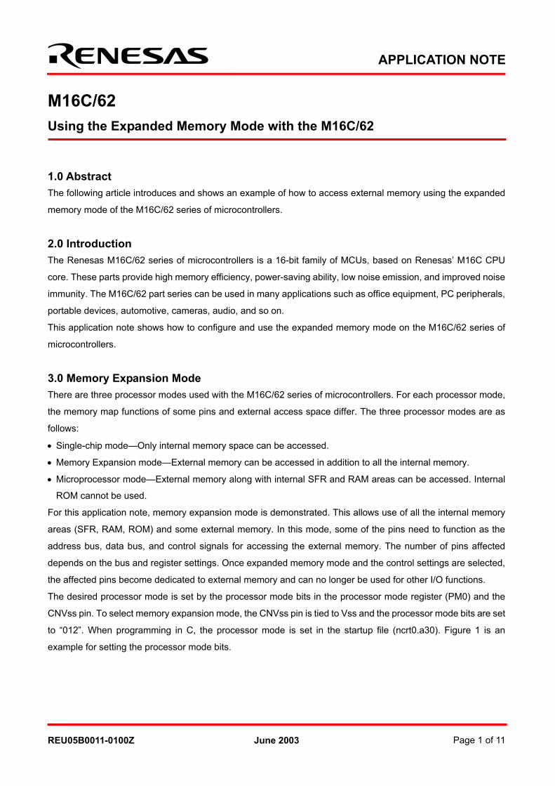
The desired processor mode is set by the processor mode bits in the processor mode register (PM0) and the
CNVss pin. To select memory expansion mode, the CNVss pin is tied to Vss and the processor mode bits are set
to “012”. When programming in C, the processor mode is set in the startup file (ncrt0.a30). Figure 1 is an
example for setting the processor mode bits.
REU05B0011-0100Z June 2003 Page 1 of 11
M16C/62Using the Expanded Memory Mode with the M16C/62
Figure 1 Setting the Processor Mode Bits in ncrt0.a30
The bus settings and control signals can also be customized for different configurations. The external bus width
can be set to either 8 bits or 16 bits by connecting the BYTE pin to Vcc or Vss respectively. This does not affect
the internal bus, which is always fixed to 16 bits.
The read/write signal configurations are set in the processor mode register (PM0). There are two combinations of
R/W signals. For a 16-bit data bus, select between the RD, WR, and BHE signals or the RD, WRL, and WRH
signals. When using an 8-bit bus, always use the RD, WR, and BHE signals.
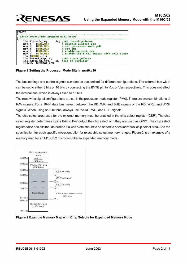
The chip select area used for the external memory must be enabled in the chip select register (CSR). The chip
select register determines if pins P44 to P47 output the chip select or if they are used as GPIO. The chip select
register also has bits that determine if a wait state should to be added to each individual chip select area. See the
specification for each specific microcontroller for exact chip select memory ranges. Figure 2 is an example of a
memory map for an M16C/62 microcontroller in expanded memory mode.
0000016
0040016
FFFFF16
D000016
0800016
Internal RAM area(15K bytes)
External area
Internal ROM area(192K bytes)
CS3(16K bytes)
CS2(128K bytes)
CS1(32K bytes)
CS0 Memory expansion mode: 640K bytes
2800016
3000016
0400016
SFR area(1K bytes)
CFFFF16
Memory expansion mode
Figure 2 Example Memory Map with Chip Selects for Expanded Memory Mode
REU05B0011-0100Z June 2003 Page 2 of 11

M16C/62Using the Expanded Memory Mode with the M16C/62
Other control signals used are the RDY and HOLD signals. The RDY signal is used for any external device that
requires a long access time. The HOLD signal is used to transfer the bus privileges from the CPU to an external
device.
Note: If the RDY and/or HOLD signals are not used, they must be connected to Vcc or the MCU could be permanently stuck in a wait state.
More detailed information on expanded memory, processor modes, and bus settings can be found in the
M16C/62 specification and user’s manual.
4.0 Using Expanded Memory with the PC4701 Emulation System Some special considerations are required when using expanded memory with the PC4701 emulator. To access
any external memory with the emulator, the external memory area must first be mapped using the
emulator/debugger software PD30. When PD30 is first started, all memory except for the SFR area is mapped as
internal memory.
First, determine the external memory range that will be used according to the chip select that is being used. This
external memory area must be mapped to external. Open a script window in PD30 and use the map command to
change the memory range that is being used to “External” (example: “map 8000, 9000, ext”). This maps the
memory range 8000h to 9000h as external memory. To check that the changes have been set, type “map” in the
command line and a list of the current memory map is displayed.
There is one precaution to observe when using the emulator and the CS2 memory space. The memory
addresses, 0FFFCh to 0FFFFh, are used by the emulator as a stack area. These addresses must remain
mapped as internal memory or the program will not reset properly. See the Emulation System manual for more
information on this precaution. shows an example of mapping the CS2 memory area around the
emulator stack.
Figure 3
Figure 3 Mapping External Memory in PD30
REU05B0011-0100Z June 2003 Page 3 of 11
M16C/62Using the Expanded Memory Mode with the M16C/62
5.0 Implementation A sample program is included to demonstrate the use of expanded memory mode. This program is written to run
on Renesas’ MDECE0620 evaluation board. This board allows easy evaluation for any M16C/62 microcontroller.
The example program samples the voltage of a potentiometer on the evaluation board and stores this data into
the external SRAM on the board. The potentiometer is connected to channel 0 of the A/D converter on the M16C.
When the push button S2 is pushed, the A/D value is sampled about every 100 ms and written to the SRAM one
byte at a time. An LED (D6) blinks to indicate when the A/D is sampling. When the push button is pressed again,
the A/D sampling will stop, all of the A/D data stored in memory is read back, and an average A/D value is
calculated. Each time the A/D sampling is started, it returns to the beginning of memory and starts storing data.
For simplicity, the sample program is limited to storing a total of 8 kbytes of data.
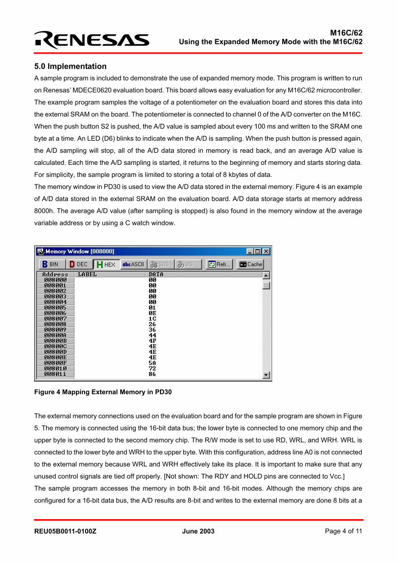
The memory window in PD30 is used to view the A/D data stored in the external memory. Figure 4 is an example
of A/D data stored in the external SRAM on the evaluation board. A/D data storage starts at memory address
8000h. The average A/D value (after sampling is stopped) is also found in the memory window at the average
variable address or by using a C watch window.
Figure 4 Mapping External Memory in PD30
The external memory connections used on the evaluation board and for the sample program are shown in
. The memory is connected using the 16-bit data bus; the lower byte is connected to one memory chip and the
upper byte is connected to the second memory chip. The R/W mode is set to use RD, WRL, and WRH. WRL is
connected to the lower byte and WRH to the upper byte. With this configuration, address line A0 is not connected
to the external memory because WRL and WRH effectively take its place. It is important to make sure that any
unused control signals are tied off properly. [Not shown: The RDY and HOLD pins are connected to Vcc.]
Figure
5
The sample program accesses the memory in both 8-bit and 16-bit modes. Although the memory chips are
configured for a 16-bit data bus, the A/D results are 8-bit and writes to the external memory are done 8 bits at a
REU05B0011-0100Z June 2003 Page 4 of 11

M16C/62Using the Expanded Memory Mode with the M16C/62
time. When A/D sampling stops, the results are read from external memory using 16-bit mode. The data are split
into two bytes and added together to calculate the average A/D value.
Chip select 2 is used to address the memory. The effective address range using CS2 is 8000h to 27FFFh; this is
a total of 128 Kbytes. Each memory chip in our demo contains 32k x 8 bits or 64 Kbytes total memory (8000h –
17FFFh).
Figure 5 External Memory Connections
The potentiometer on the evaluation board is connected to A/D input AN0 on the M16C/62. The A/D is set up for
8-bit conversion, one-shot mode, software triggered, with sample and hold enabled.
The push button (S2) used to start and stop the A/D sampling is connected to an external interrupt on the M16/62.
The interrupt used is INT0. Each time the push button is pressed, an INT0 interrupt is generated. A flag monitors
the A/D sampling when it is on or off.
The LCD supplied on the evaluation board views the A/D values as they are sampled and the average A/D value
when sampling is stopped. Because some of the LCD connections on the board are used for control signals in
expanded memory mode, some circuit modifications are needed for the LCD to work with external memory.
shows the LCD connections used in the sample program. This configuration allows the LCD to be
accessed similar to any external memory. Chip select 1 addresses the LCD, thus writing to any even address
(low byte in 16-bit address bus) in the CS1 memory area writes data to the LCD. Writing to an even address
causes the WRL signal to go to a logic low level. Writing to an odd address causes WRH to go to a logic low, and
Figure 6
REU05B0011-0100Z June 2003 Page 5 of 11

M16C/62Using the Expanded Memory Mode with the M16C/62
does not enable the LCD. In the sample program the address 28000h is used.
Figure 6 MDECE0620 LCD Connections When Using External Memory
The sample program is just one way of using expanded memory mode on the M16C/62 series of
microcontrollers.
6.0 Reference
Renesas Technology Corporation Semiconductor Home Page
http://www.renesas.com
E-mail Support
Data Sheets
• M16C/62 datasheets, 62aeds.pdf
REU05B0011-0100Z June 2003 Page 6 of 11
M16C/62Using the Expanded Memory Mode with the M16C/62
7.0 Software Code /***************************************************************************** * * File Name: main.c * * Content: This program demonstrates using expanded memory on the * MDECE0620 evaluation bd. When S2 is pressed, A/D measurements * are taken from R11 (pot.) at 100ms intervals and stored in * external memory. When S2 is pressed again, the A/D sampling * stops, the data is read from memory and an average A/D value * is calculated. * * Date: 9-28-2001 * * Copyright 2003 Renesas Technology Corporation * All rights reserved * *============================================================================= * $Log:$ *===========================================================================*/ #include "sfr62.h" /* include 620 header file */ #include "lcd_exp.h" /* lcd include file */ /* Setup interrupt routine for INT0 This must also be setup in the vector table in SECT30.INC */ #pragma INTERRUPT /B INT0_ISR /* Prototypes */ void Get_Avg (void); void LCD_write (_far char *, int); /* Global variables */ unsigned int mem_start = 0x8000; /* declare expanded memory start address */ unsigned char *mem_ptr; /* declare memory pointer */ unsigned int *word_ptr; /* declare word memory pointer */ unsigned char ad_on = 0; /* A/D sampling flag */ unsigned int sample_cnt = 0; /* sample counter */ union word_define { /* define word structure */ struct{ char low; /* low 8 bit */ char high; /* high 8 bit */ }byte; unsigned int word; } memory; /* String Messages */ const char msg_text1[] = "Expanded Memory"; /* LCD messages */ const char msg_text2[] = "Demo Program";
REU05B0011-0100Z June 2003 Page 7 of 11

M16C/62Using the Expanded Memory Mode with the M16C/62
const char msg_ad[] = "A/D Value"; const char msg_avg[] = "A/D Average"; /***************************************************************************** Name: Main Parameters: Returns: Description: This is the main program *****************************************************************************/ void main() { int temp; unsigned int delay; unsigned char ad_data; mem_ptr = (unsigned char *) mem_start; /* Initialize Ports */ pd7 = 0xFF; /* Configure port 7 as all outputs */ p7 |= 0x80; /* Initialize port7_4 to 7_7, LEDs off */ pd8 = 0x02; /* port 8_1 output */ p8_1 = 0; /* Initialize p8_1 (LCD RS) */ pd10 = 0; /* A/D input */ /* Use A/D for reading pot. value */ adcon0 = 0x00; /* AN0 ,one shot mode,software trigger,freq /4*/ adcon1 = 0x20; /* Set up 8 bit conversion & Vref connected */ adcon2 = 0x01; /* Set up sample and hold */ /* Initialize Timer A4 for S2 switch debounce */ ta4ic = 0x00; /* make sure that the interrupt is not active */ ta4mr = 0x82; /* set for one shot timer mode */ ta4 = 0xffff; /* Debounce time delay */ ta4s = 1; /* get ready */ ta4os = 1; /* start timer once */ LCD_init(); /* Initialize LCD display */ int0ic = 0x05; /* Enable INT0 interrupt */ asm("FSET I"); /* Enable all interrupts */ LCD_write( msg_text1, 1 ); /* Intial LCD message */ LCD_write( msg_text2, 2 ); /**************** PROGRAM LOOP **************************/ while (1){ if (ad_on == 1){ p7_7 = ~p7_7; /* blink LED to indicate A/D sampling */ L2homeLCD(); /* Home LCD on line 2 */ adst = 1; /* Start A/D conversion */ while(adst == 1); /* wait for A/D conversion start bit to return to 0 */
REU05B0011-0100Z June 2003 Page 8 of 11

M16C/62Using the Expanded Memory Mode with the M16C/62
ad_data = ad0; /* read value from A/D register */ *mem_ptr = ad_data; /* save A/D data to memory */ mem_ptr++; /* increment memory pointer */ sample_cnt++; /* increment sample counter */ LCD_DisplayHex(ad_data); /* Output data to LCD */ if (sample_cnt >= 0x2000){ /* limit samples to 8k bytes */ ad_on = 0; /* stop sampling */ p7_7 = 1; /* stop LED blinking */ Get_Avg (); /* calculate average A/D value */ } } for (delay=0x2aff; delay>0; delay--); /* sampling delay ~100ms */ } } /******************** END OF MAIN *******************************************/ /***************************************************************************** Name: INT0_ISR Parameters: Returns: Description: INT0 interrupt routine, S2 is connected to INT0 S2 controls when A/D sampling starts and stops *****************************************************************************/ void INT0_ISR(void) { if (ir_ta4ic == 0) /* Switch Debounce timer timeout? */ return; /* If not return, do nothing */ int0ic = 0x00; /* disable INT0 interrupt */ /* Start A/D sampling */ if(ad_on == 0){ /* A/D sampling currently off?*/ ad_on = 1; /* turn on */ mem_ptr = (unsigned char *) mem_start; /* Reset memory to begining */ sample_cnt = 0; /* Reset sample counter */ clrLCD (); /* clear LCD */ LCD_write( msg_ad, 1 ); /* change LCD display */ } /* Stop A/D sampling */ else if (ad_on == 1){ /* A/D sampling currently on ? */ ad_on = 0; /* turn off */ p7_7 = 1; /* stop LED blinking */ Get_Avg (); /* calculate average A/D value */
REU05B0011-0100Z June 2003 Page 9 of 11
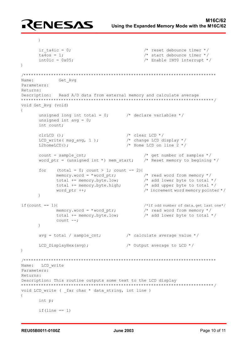
M16C/62Using the Expanded Memory Mode with the M16C/62
} ir_ta4ic = 0; /* reset debounce timer */ ta4os = 1; /* start debounce timer */ int0ic = 0x05; /* Enable INT0 interrupt */ } /***************************************************************************** Name: Get_Avg Parameters: Returns: Description: Read A/D data from external memory and calculate average *****************************************************************************/ void Get_Avg (void) { unsigned long int total = 0; /* declare variables */ unsigned int avg = 0; int count; clrLCD (); /* clear LCD */ LCD_write( msg_avg, 1 ); /* change LCD display */ L2homeLCD(); /* Home LCD on line 2 */ count = sample_cnt; /* get number of samples */ word_ptr = (unsigned int *) mem_start; /* Reset memory to begining */ for (total = 0; count > 1; count -= 2){ memory.word = *word_ptr; /* read word from memory */ total += memory.byte.low; /* add lower byte to total */ total += memory.byte.high; /* add upper byte to total */ word_ptr ++; /* increment word memory pointer */ } if(count == 1){ /*if odd number of data,get last one*/ memory.word = *word_ptr; /* read word from memory */ total += memory.byte.low; /* add lower byte to total */ count --; } avg = total / sample_cnt; /* calculate average value */ LCD_DisplayHex(avg); /* Output average to LCD */ } /***************************************************************************** Name: LCD_write Parameters: Returns: Description: This routine outputs some text to the LCD display *****************************************************************************/ void LCD_write ( _far char * data_string, int line ) { int p; if(line == 1)
REU05B0011-0100Z June 2003 Page 10 of 11

M16C/62Using the Expanded Memory Mode with the M16C/62
L1homeLCD(); /* home display on line 1*/ else L2homeLCD(); /* home display on line 2*/ for (p=0; data_string[p]; p++){ /* This loop reads in the text string */ SendChar(data_string[p]); } }
REU05B0011-0100Z June 2003 Page 11 of 11

Keep safety first in your circuit designs!
• Renesas Technology Corporation puts the maximum effort into making semiconductor products
better and more reliable, but there is always the possibility that trouble may occur with them. Trouble with semiconductors may lead to personal injury, fire or property damage. Remember to give due consideration to safety when making your circuit designs, with appropriate measures such as (i) placement of substitutive, auxiliary circuits, (ii) use of nonflammable material or (iii) prevention against any malfunction or mishap.
Notes regarding these materials
• These materials are intended as a reference to assist our customers in the selection of the Renesas Technology Corporation product best suited to the customer's application; they do not convey any license under any intellectual property rights, or any other rights, belonging to Renesas Technology Corporation or a third party.
• Renesas Technology Corporation assumes no responsibility for any damage, or infringement of any third-party's rights, originating in the use of any product data, diagrams, charts, programs, algorithms, or circuit application examples contained in these materials.
• All information contained in these materials, including product data, diagrams, charts, programs and algorithms represents information on products at the time of publication of these materials, and are subject to change by Renesas Technology Corporation without notice due to product improvements or other reasons. It is therefore recommended that customers contact Renesas Technology Corporation or an authorized Renesas Technology Corporation product distributor for the latest product information before purchasing a product listed herein. The information described here may contain technical inaccuracies or typographical errors. Renesas Technology Corporation assumes no responsibility for any damage, liability, or other loss rising from these inaccuracies or errors. Please also pay attention to information published by Renesas Technology Corporation by various means, including the Renesas Technology Corporation Semiconductor home page (http://www.renesas.com).
• When using any or all of the information contained in these materials, including product data, diagrams, charts, programs, and algorithms, please be sure to evaluate all information as a total system before making a final decision on the applicability of the information and products. Renesas Technology Corporation assumes no responsibility for any damage, liability or other loss resulting from the information contained herein.
• Renesas Technology Corporation semiconductors are not designed or manufactured for use in a device or system that is used under circumstances in which human life is potentially at stake. Please contact Renesas Technology Corporation or an authorized Renesas Technology Corporation product distributor when considering the use of a product contained herein for any specific purposes, such as apparatus or systems for transportation, vehicular, medical, aerospace, nuclear, or undersea repeater use.
• The prior written approval of Renesas Technology Corporation is necessary to reprint or reproduce in whole or in part these materials.
• If these products or technologies are subject to the Japanese export control restrictions, they must be exported under a license from the Japanese government and cannot be imported into a country other than the approved destination. Any diversion or reexport contrary to the export control laws and regulations of Japan and/or the country of destination is prohibited.
• Please contact Renesas Technology Corporation for further details on these materials or the products contained therein.