Using Parallax TSL1401-DB Linescan Camera Module for line...
17
1 Introduction This application note explains how the Parallax TSL1401-DB camera works and how it can be used for the specific application of following a line for the Smart Car Race competition. This document includes tips and refers to the example code on how to process the signal from the camera on the MPC5604B microcontroller (MCU); the example code can be downloaded as AN4244SW from https:// www.freescale.com. The Parallax TSL1401-DB LineScan Camera Module consist of a CMOS linear sensor of 128 pixel array and a mounted lens of 7.9 mm, these provide a field of view equal to the subject distance. Some of the advantages of using this camera are the following: • Simple and easy to use • Frequency of capture can be manipulated by the user • Enough definition for line following application • Removable and interchangeable lens for different resolutions Besides the above benefits, the only disadvantage is the output signal of the camera is completely analog, which means the user has to be creative, to process this signal in order to make it “understandable”. This document provides two different methods to process this signal. There are many evaluation boards for the Parallax camera, which can be another inconvenience. For this case, a benchmark was done and “Parallax BASIC Stamp DB- Freescale Semiconductor Document Number: MPC5604B Application Note Rev. 0, 01/2011 Using Parallax TSL1401-DB Linescan Camera Module for line detection Example code based on the MPC5604B MCU by: Francisco Ramirez Fuentes, Marco Trujillo, Cuauhtli Padilla, Rodrigo Mendoza © 2010 Freescale Semiconductor, Inc. Contents 1 Introduction.................................................................1 2 Camera signal interpretation.......................................2 3 Signal processing........................................................3 4 Software/Driver description........................................5 5 AO signal processing implementation........................8 6 Conclusion................................................................16
-
Upload
vuongquynh -
Category
Documents
-
view
260 -
download
4
Transcript of Using Parallax TSL1401-DB Linescan Camera Module for line...
1 IntroductionThis application note explains how the Parallax TSL1401-DBcamera works and how it can be used for the specificapplication of following a line for the Smart Car Racecompetition. This document includes tips and refers to theexample code on how to process the signal from the camera onthe MPC5604B microcontroller (MCU); the example code canbe downloaded as AN4244SW from https://www.freescale.com. The Parallax TSL1401-DB LineScanCamera Module consist of a CMOS linear sensor of 128 pixelarray and a mounted lens of 7.9 mm, these provide a field ofview equal to the subject distance. Some of the advantages ofusing this camera are the following:
• Simple and easy to use• Frequency of capture can be manipulated by the user• Enough definition for line following application• Removable and interchangeable lens for different
resolutions
Besides the above benefits, the only disadvantage is the outputsignal of the camera is completely analog, which means theuser has to be creative, to process this signal in order to makeit “understandable”. This document provides two differentmethods to process this signal.
There are many evaluation boards for the Parallax camera,which can be another inconvenience. For this case, abenchmark was done and “Parallax BASIC Stamp DB-
Freescale Semiconductor Document Number: MPC5604B
Application Note Rev. 0, 01/2011
Using Parallax TSL1401-DBLinescan Camera Module for linedetectionExample code based on the MPC5604B MCU
by: Francisco Ramirez Fuentes, Marco Trujillo, Cuauhtli Padilla, RodrigoMendoza
© 2010 Freescale Semiconductor, Inc.
Contents
1 Introduction.................................................................1
2 Camera signal interpretation.......................................2
3 Signal processing........................................................3
4 Software/Driver description........................................5
5 AO signal processing implementation........................8
6 Conclusion................................................................16
Expander Daughter board-to-SIP” or the “Parallax Stamp 2pe Daughter board Extension Cable” was found. These werefound as the easiest to use from https://www.parallax.com.
NOTERev 0 of this application note provides only the drivers as explained in the example code. A completeexample using these drivers will be provided in the next revision of the application note.
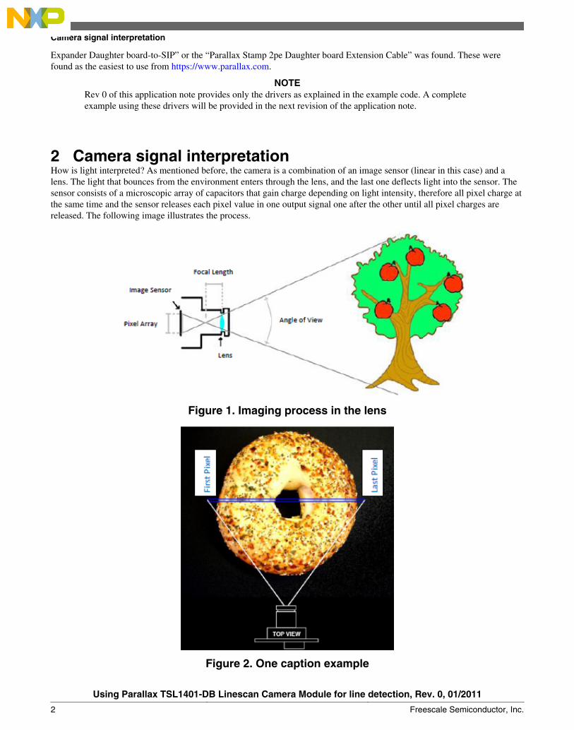
2 Camera signal interpretationHow is light interpreted? As mentioned before, the camera is a combination of an image sensor (linear in this case) and alens. The light that bounces from the environment enters through the lens, and the last one deflects light into the sensor. Thesensor consists of a microscopic array of capacitors that gain charge depending on light intensity, therefore all pixel charge atthe same time and the sensor releases each pixel value in one output signal one after the other until all pixel charges arereleased. The following image illustrates the process.
Figure 1. Imaging process in the lens
Figure 2. One caption example
Camera signal interpretation
Using Parallax TSL1401-DB Linescan Camera Module for line detection, Rev. 0, 01/2011
2 Freescale Semiconductor, Inc.
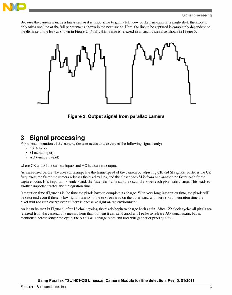
Because the camera is using a linear sensor it is impossible to gain a full view of the panorama in a single shot, therefore itonly takes one line of the full panorama as shown in the next image. Here, the line to be captured is completely dependent onthe distance to the lens as shown in Figure 2. Finally this image is released in an analog signal as shown in Figure 3.
Figure 3. Output signal from parallax camera
3 Signal processingFor normal operation of the camera, the user needs to take care of the following signals only:
• CK (clock)• SI (serial input)• AO (analog output)
where CK and SI are camera inputs and AO is a camera output.
As mentioned before, the user can manipulate the frame speed of the camera by adjusting CK and SI signals. Faster is the CKfrequency, the faster the camera releases the pixel values, and the closer each SI is from one another the faster each framecapture occur. It is important to understand, the faster the frame capture occur the lower each pixel gain charge. This leads toanother important factor, the “integration time”.
Integration time (Figure 4) is the time the pixels have to complete its charge. With very long integration time, the pixels willbe saturated even if there is low light intensity in the environment, on the other hand with very short integration time thepixel will not gain charge even if there is excessive light on the environment.
As it can be seen in Figure 4, after 18 clock cycles, the pixels begin to charge back again. After 129 clock cycles all pixels arereleased from the camera, this means, from that moment it can send another SI pulse to release AO signal again; but asmentioned before longer the cycle, the pixels will charge more and user will get better pixel quality.
Signal processing
Using Parallax TSL1401-DB Linescan Camera Module for line detection, Rev. 0, 01/2011
Freescale Semiconductor, Inc. 3
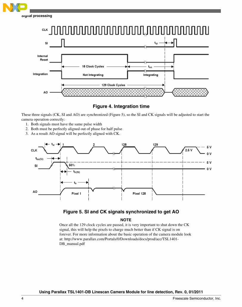
Figure 4. Integration time
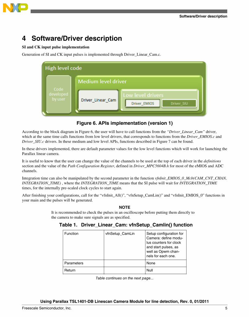
These three signals (CK, SI and AO) are synchronized (Figure 5), so the SI and CK signals will be adjusted to start thecamera operation correctly:
1. Both signals must have the same pulse width2. Both must be perfectly aligned out of phase for half pulse3. As a result AO signal will be perfectly aligned with CK.
Figure 5. SI and CK signals synchronized to get AO
NOTEOnce all the 129 clock cycles are passed, it is very important to shut down the CKsignal, this will help the pixels to charge much better than if CK signal is onforever. For more information about the basic operation of the camera module lookat: http://www.parallax.com/Portals/0/Downloads/docs/prod/acc/TSL1401-DB_manual.pdf
Signal processing
Using Parallax TSL1401-DB Linescan Camera Module for line detection, Rev. 0, 01/2011
4 Freescale Semiconductor, Inc.
4 Software/Driver descriptionSI and CK input pulse implementation
Generation of SI and CK input pulses is implemented through Driver_Linear_Cam.c.
Figure 6. APIs implementation (version 1)
According to the block diagram in Figure 6, the user will have to call functions from the “Driver_Linear_Cam” driver,which at the same time calls functions from low level drivers, that corresponds to functions from the Driver_EMIOS.c andDriver_SIU.c drivers. In these medium and low level APIs, functions described in Figure 7 can be found.
In these drivers implemented, there are default parameter values for the low level functions which will work for launching theParallax linear camera.
It is useful to know that the user can change the value of the channels to be used at the top of each driver in the definitionssection and the value of the Path Configuration Register, defined in Driver_MPC5604B.h for most of the eMIOS and ADCchannels.
Integration time can also be manipulated by the second parameter in the function vfnInit_EMIOS_0_Mcb(CAM_CNT_CHAN,INTEGRATION_TIME) , where the INTEGRATION_TIME means that the SI pulse will wait for INTEGRATION_TIMEtimes, for the internally pre-scaled clock cycles to start again.
After finishing your configurations, call for the “vfnInit_All()”, “vfnSetup_CamLin()” and “vfnInit_EMIOS_0” functions inyour main and the pulses will be generated.
NOTEIt is recommended to check the pulses in an oscilloscope before putting them directly tothe camera to make sure signals are as specified.
Table 1. Driver_Linear_Cam: vfnSetup_Camlin() function
Function vfnSetup_CamLin Setup configuration forCamera: define modu‐lus counters for clockand start pulses, aswell as Opwm chan‐nels for each one.
Parameters None
Return Null
Table continues on the next page...
Software/Driver description
Using Parallax TSL1401-DB Linescan Camera Module for line detection, Rev. 0, 01/2011
Freescale Semiconductor, Inc. 5
Table 1. Driver_Linear_Cam: vfnSetup_Camlin() function (continued)
Functions from SIU vfnInit_Emios_Out‐put_Pad
Initialize a microcon‐troller pin as an outputfor an EMIOS channel.
Functions from EMIOS vfnSetup_Emios_0 Enable Emios clock,configure preescaler togenerate 4 MHz Emiosclock, enable globaltime base, enableFreezing channel tofreeze them when indebug mode.
vfnInit_Emios_0_Mcb Define Emios channelas Modulus up counterbuffered with period se‐lected by the A param‐eter, configure pre‐escaler to produce 1MHz time base.
vfnI‐nit_Emios_0_Opwm
Define Emios channelas positive Opwm withtime base correspond‐ing to the counter busB,C,D,or E and estab‐lish its raising and fall‐ing edge with parame‐ters A and B.
Definitions involved CAM_CNT_CHAN Emios channel used asModulus Counter for SIsignal.
CHANNEL_CK Emios channel used togenerate CK signal forcamera.
CHANNEL_SI Emios channel used togenerate SI signal forcamera.
PCR_EMIOS_0_tag Pad configuration reg‐ister required to config‐ure SIU module. De‐fined in “Driv‐er_MPC5604B”.
Focusing the camera
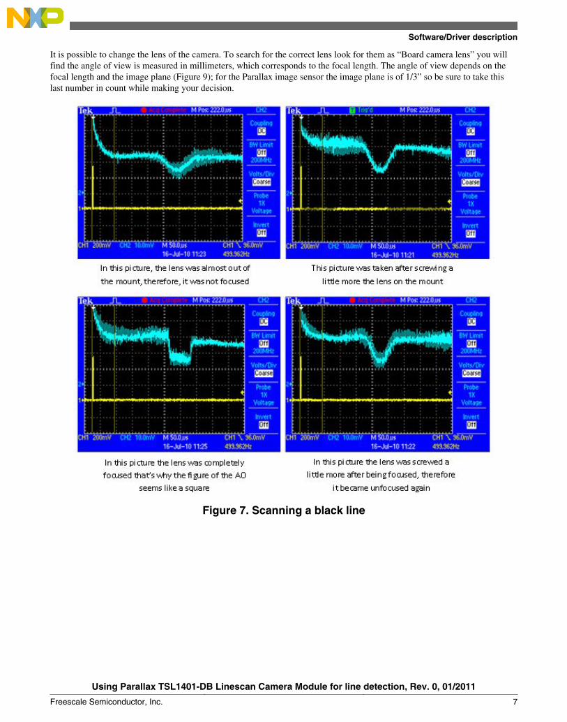
Once the sensor is perfectly working the next step is to find the best position of the lens that will generate the clearest images.The best way to do it is using an oscilloscope (Figure 8);
1. Connect the SI and AO signals to the oscilloscope2. Set the SI pulse so that it can be clearly seen and then trig the AO signal with the SI signal using the trig function3. Fix the camera looking at a sheet of paper with a black line in the center4. The image of the black line will appear on the oscilloscope screen5. Screw the camera until you find the position where the line seems the clearest
Software/Driver description
Using Parallax TSL1401-DB Linescan Camera Module for line detection, Rev. 0, 01/2011
6 Freescale Semiconductor, Inc.
It is possible to change the lens of the camera. To search for the correct lens look for them as “Board camera lens” you willfind the angle of view is measured in millimeters, which corresponds to the focal length. The angle of view depends on thefocal length and the image plane (Figure 9); for the Parallax image sensor the image plane is of 1/3” so be sure to take thislast number in count while making your decision.
Figure 7. Scanning a black line
Software/Driver description
Using Parallax TSL1401-DB Linescan Camera Module for line detection, Rev. 0, 01/2011
Freescale Semiconductor, Inc. 7
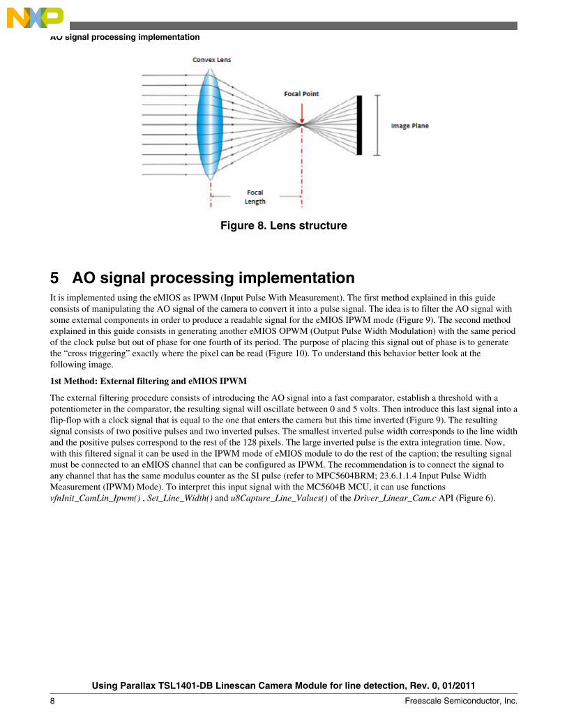
Figure 8. Lens structure
5 AO signal processing implementationIt is implemented using the eMIOS as IPWM (Input Pulse With Measurement). The first method explained in this guideconsists of manipulating the AO signal of the camera to convert it into a pulse signal. The idea is to filter the AO signal withsome external components in order to produce a readable signal for the eMIOS IPWM mode (Figure 9). The second methodexplained in this guide consists in generating another eMIOS OPWM (Output Pulse Width Modulation) with the same periodof the clock pulse but out of phase for one fourth of its period. The purpose of placing this signal out of phase is to generatethe “cross triggering” exactly where the pixel can be read (Figure 10). To understand this behavior better look at thefollowing image.
1st Method: External filtering and eMIOS IPWM
The external filtering procedure consists of introducing the AO signal into a fast comparator, establish a threshold with apotentiometer in the comparator, the resulting signal will oscillate between 0 and 5 volts. Then introduce this last signal into aflip-flop with a clock signal that is equal to the one that enters the camera but this time inverted (Figure 9). The resultingsignal consists of two positive pulses and two inverted pulses. The smallest inverted pulse width corresponds to the line widthand the positive pulses correspond to the rest of the 128 pixels. The large inverted pulse is the extra integration time. Now,with this filtered signal it can be used in the IPWM mode of eMIOS module to do the rest of the caption; the resulting signalmust be connected to an eMIOS channel that can be configured as IPWM. The recommendation is to connect the signal toany channel that has the same modulus counter as the SI pulse (refer to MPC5604BRM; 23.6.1.1.4 Input Pulse WidthMeasurement (IPWM) Mode). To interpret this input signal with the MC5604B MCU, it can use functionsvfnInit_CamLin_Ipwm() , Set_Line_Width() and u8Capture_Line_Values() of the Driver_Linear_Cam.c API (Figure 6).
AO signal processing implementation
Using Parallax TSL1401-DB Linescan Camera Module for line detection, Rev. 0, 01/2011
8 Freescale Semiconductor, Inc.
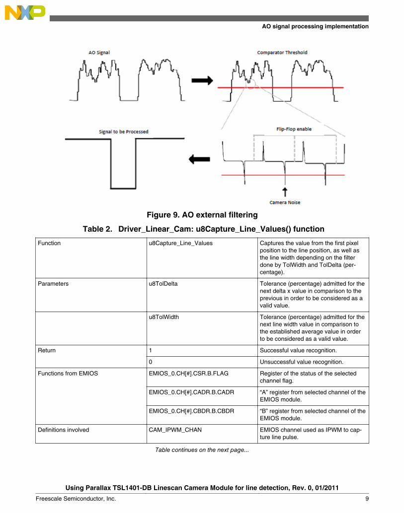
Figure 9. AO external filtering
Table 2. Driver_Linear_Cam: u8Capture_Line_Values() function
Function u8Capture_Line_Values Captures the value from the first pixelposition to the line position, as well asthe line width depending on the filterdone by TolWidth and TolDelta (per‐centage).
Parameters u8TolDelta Tolerance (percentage) admitted for thenext delta x value in comparison to theprevious in order to be considered as avalid value.
u8TolWidth Tolerance (percentage) admitted for thenext line width value in comparison tothe established average value in orderto be considered as a valid value.
Return 1 Successful value recognition.
0 Unsuccessful value recognition.
Functions from EMIOS EMIOS_0.CH[#].CSR.B.FLAG Register of the status of the selectedchannel flag.
EMIOS_0.CH[#].CADR.B.CADR “A” register from selected channel of theEMIOS module.
EMIOS_0.CH[#].CBDR.B.CBDR “B” register from selected channel of theEMIOS module.
Definitions involved CAM_IPWM_CHAN EMIOS channel used as IPWM to cap‐ture line pulse.
Table continues on the next page...
AO signal processing implementation
Using Parallax TSL1401-DB Linescan Camera Module for line detection, Rev. 0, 01/2011
Freescale Semiconductor, Inc. 9
Table 2. Driver_Linear_Cam: u8Capture_Line_Values() function (continued)
Variables involved u16center Global variable used to save the valueof the position of the line center beforefilter.
u16width Local variable used to save the value ofthe line width before filter.
u16LineWidthMeasure Global variable used to compare actualline width with established average linewidth for filtering.
u16LineWidth Global variable used to save the valueof the line width after filter.
u16Center Global variable used to save the valueof the position of the line center after fil‐ter.
Table 3. Driver_Linear_Cam: Set_Line_Width()function
Function Set_Line_Width Define the value of an average linewidth from selected samples, define theactual delta X value as a result of anaverage of the same samples.
Parameters u8Frames Number of desired samples to calculatevariables.
Return Null
Functions from EMIOS EMIOS_0.CH[#].CSR.B.FLAG Register of the status of the selectedchannel flag.
EMIOS_0.CH[#].CADR.B.CADR “A” register from selected channel of theEMIOS module.
EMIOS_0.CH[#].CBDR.B.CBDR “B” register from selected channel of theEMIOS module.
Definitions involved CAM_IPWM_CHAN EMIOS channel used as IPWM to cap‐ture line pulse.
Variables involved i Local variable as counter for capturingrequested number of frames.
u16LineWidthMeasure Global variable that gets the value of theaverage width of the line.
u16Center Global variable that gets the value of theaverage position of the center of theline.
Table 4. Driver_Linear_Cam: vfnInit_CamLin_Ipwm() function
Function vfnInit_CamLin_Ipwm Set global variables to 0 and define anEmios channel as IPWM with selectedpolarity.
Parameters None
Table continues on the next page...
AO signal processing implementation
Using Parallax TSL1401-DB Linescan Camera Module for line detection, Rev. 0, 01/2011
10 Freescale Semiconductor, Inc.
Table 4. Driver_Linear_Cam: vfnInit_CamLin_Ipwm() function (continued)
Return Null
Functions from SIU vfnInit_Emios_Input_Pad Initialize a microcontroller pin as an in‐put for an EMIOS channel.
Functions from EMIOS vfnInit_Emios_0_Ipwm Define Emios channel as IPWM with se‐lected polarity and time base corre‐sponding to the counter bus B,C,D,or E.
Definitions involved PCR_EMIOS_0_tag Pad configuration register required toconfigure SIU module. Defined in “Driv‐er_MPC5604B”.
Variables involved u16LineWidthMeasure Global variable set to 0.
u16Center Global variable set to 0.
u16LineWidth Global variable set to 0.
To obtain the values of line width and position of the line for the high level algorithm it is necessary to call functionsu16_LineWidth() and u16_Center(). These are just return functions for the u16LineWidth and the u16Center variables.
Table 5. Advantage and disadvantage of external filtering and eMIOS IPWM
Advantage Disadvantage
Fast and easy process for the MCU Needs external analog processing
ADC module is free for other applications Have many calibration conflicts
2nd Method: Processing with ADC and CTU
For this method, CTU (Cross Triggering Unit) will be used. As the CTU is in charge of triggering between eMIOS and ADCmodules, it can start an ADC conversion when a eMIOS module flag is activated. As mentioned before; it is being generatedas eMIOS OPWM with the same period of the clock pulse but out of phase for one fourth of its period. The purpose ofplacing this signal out of phase is to generate the “cross triggering” exactly where the pixel can be read (Figure 10). The CTUsignal will trigger the ADC conversion when the pixel charge is in good conditions to be read, for this reason it is importantto align these signals as shown in Figure 10. For capturing pixel values and developing useful data, use thevfnInit_CamLin_Adc() and u8Capture_Pixel_Values() functions of the Driver_Linear_Cam.c driver (Figure 11).
AO signal processing implementation
Using Parallax TSL1401-DB Linescan Camera Module for line detection, Rev. 0, 01/2011
Freescale Semiconductor, Inc. 11
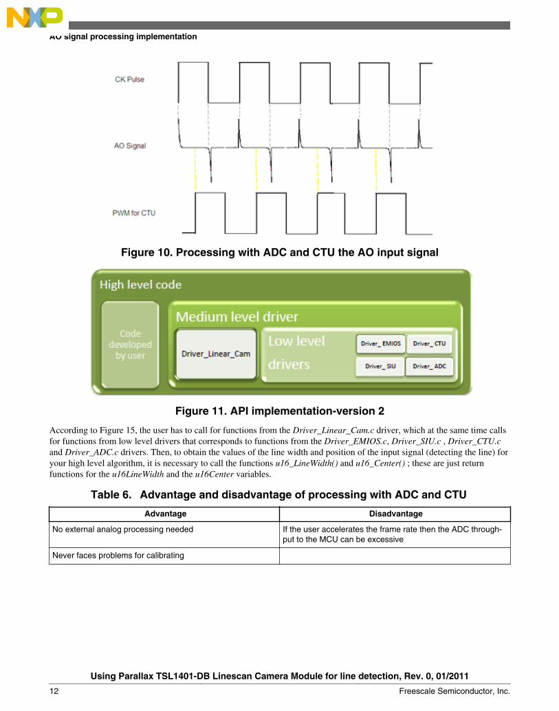
Figure 10. Processing with ADC and CTU the AO input signal
Figure 11. API implementation-version 2
According to Figure 15, the user has to call for functions from the Driver_Linear_Cam.c driver, which at the same time callsfor functions from low level drivers that corresponds to functions from the Driver_EMIOS.c, Driver_SIU.c , Driver_CTU.cand Driver_ADC.c drivers. Then, to obtain the values of the line width and position of the input signal (detecting the line) foryour high level algorithm, it is necessary to call the functions u16_LineWidth() and u16_Center() ; these are just returnfunctions for the u16LineWidth and the u16Center variables.
Table 6. Advantage and disadvantage of processing with ADC and CTU
Advantage Disadvantage
No external analog processing needed If the user accelerates the frame rate then the ADC through‐put to the MCU can be excessive
Never faces problems for calibrating
AO signal processing implementation
Using Parallax TSL1401-DB Linescan Camera Module for line detection, Rev. 0, 01/2011
12 Freescale Semiconductor, Inc.
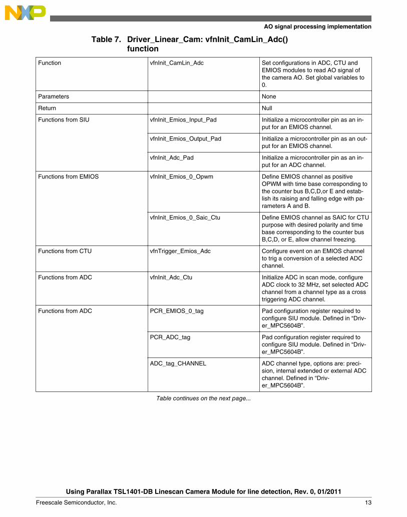
Table 7. Driver_Linear_Cam: vfnInit_CamLin_Adc()function
Function vfnInit_CamLin_Adc Set configurations in ADC, CTU andEMIOS modules to read AO signal ofthe camera AO. Set global variables to0.
Parameters None
Return Null
Functions from SIU vfnInit_Emios_Input_Pad Initialize a microcontroller pin as an in‐put for an EMIOS channel.
vfnInit_Emios_Output_Pad Initialize a microcontroller pin as an out‐put for an EMIOS channel.
vfnInit_Adc_Pad Initialize a microcontroller pin as an in‐put for an ADC channel.
Functions from EMIOS vfnInit_Emios_0_Opwm Define EMIOS channel as positiveOPWM with time base corresponding tothe counter bus B,C,D,or E and estab‐lish its raising and falling edge with pa‐rameters A and B.
vfnInit_Emios_0_Saic_Ctu Define EMIOS channel as SAIC for CTUpurpose with desired polarity and timebase corresponding to the counter busB,C,D, or E, allow channel freezing.
Functions from CTU vfnTrigger_Emios_Adc Configure event on an EMIOS channelto trig a conversion of a selected ADCchannel.
Functions from ADC vfnInit_Adc_Ctu Initialize ADC in scan mode, configureADC clock to 32 MHz, set selected ADCchannel from a channel type as a crosstriggering ADC channel.
Functions from ADC PCR_EMIOS_0_tag Pad configuration register required toconfigure SIU module. Defined in “Driv‐er_MPC5604B”.
PCR_ADC_tag Pad configuration register required toconfigure SIU module. Defined in “Driv‐er_MPC5604B”.
ADC_tag_CHANNEL ADC channel type, options are: preci‐sion, internal extended or external ADCchannel. Defined in “Driv‐er_MPC5604B”.
Table continues on the next page...
AO signal processing implementation
Using Parallax TSL1401-DB Linescan Camera Module for line detection, Rev. 0, 01/2011
Freescale Semiconductor, Inc. 13
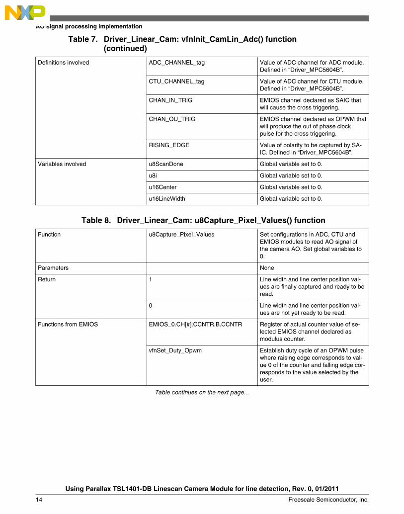
Table 7. Driver_Linear_Cam: vfnInit_CamLin_Adc() function(continued)
Definitions involved ADC_CHANNEL_tag Value of ADC channel for ADC module.Defined in “Driver_MPC5604B”.
CTU_CHANNEL_tag Value of ADC channel for CTU module.Defined in “Driver_MPC5604B”.
CHAN_IN_TRIG EMIOS channel declared as SAIC thatwill cause the cross triggering.
CHAN_OU_TRIG EMIOS channel declared as OPWM thatwill produce the out of phase clockpulse for the cross triggering.
RISING_EDGE Value of polarity to be captured by SA‐IC. Defined in “Driver_MPC5604B”.
Variables involved u8ScanDone Global variable set to 0.
u8i Global variable set to 0.
u16Center Global variable set to 0.
u16LineWidth Global variable set to 0.
Table 8. Driver_Linear_Cam: u8Capture_Pixel_Values() function
Function u8Capture_Pixel_Values Set configurations in ADC, CTU andEMIOS modules to read AO signal ofthe camera AO. Set global variables to0.
Parameters None
Return 1 Line width and line center position val‐ues are finally captured and ready to beread.
0 Line width and line center position val‐ues are not yet ready to be read.
Functions from EMIOS EMIOS_0.CH[#].CCNTR.B.CCNTR Register of actual counter value of se‐lected EMIOS channel declared asmodulus counter.
vfnSet_Duty_Opwm Establish duty cycle of an OPWM pulsewhere raising edge corresponds to val‐ue 0 of the counter and falling edge cor‐responds to the value selected by theuser.
Table continues on the next page...
AO signal processing implementation
Using Parallax TSL1401-DB Linescan Camera Module for line detection, Rev. 0, 01/2011
14 Freescale Semiconductor, Inc.
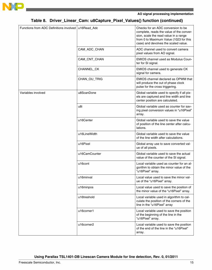
Table 8. Driver_Linear_Cam: u8Capture_Pixel_Values() function (continued)
Functions from ADC Definitions involved u16Read_Adc Checks for an ADC conversion to becomplete, reads the value of the conver‐sion, scale the read value in a rangefrom 0 to Maximum Value (1023 for thiscase) and devolves the scaled value.
CAM_ADC_CHAN ADC channel used to convert camerapixel values from AO signal.
CAM_CNT_CHAN EMIOS channel used as Modulus Coun‐ter for SI signal.
CHANNEL_CK EMIOS channel used to generate CKsignal for camera.
CHAN_OU_TRIG EMIOS channel declared as OPWM thatwill produce the out of phase clockpulse for the cross triggering.
Variables involved u8ScanDone Global variable used to specify if all pix‐els are captured and line width and linecenter position are calculated.
u8i Global variable used as counter for sav‐ing pixel conversion values in “u16Pixel”array.
u16Center Global variable used to save the valueof position of the line center after calcu‐lations.
u16LineWidth Global variable used to save the valueof the line width after calculations.
u16Pixel Global array use to save converted val‐ue of all pixels.
u16CamCounter Global variable used to save the actualvalue of the counter of the SI signal.
u16cont Local variable used as counter for an al‐gorithm to obtain the minor value of the“u16Pixel” array.
u16minval Local value used to save the minor val‐ue of the “u16Pixel” array.
u16minpos Local value used to save the position ofthe minor value of the “u16Pixel” array.
u16treshold Local variable used in algorithm to cal‐culate the position of the corners of theline in the “u16Pixel” array
u16corner1 Local variable used to save the positionof the beginning of the line in the“u16Pixel” array.
u16corner2 Local variable used to save the positionof the end of the line in the “u16Pixel”array.
AO signal processing implementation
Using Parallax TSL1401-DB Linescan Camera Module for line detection, Rev. 0, 01/2011
Freescale Semiconductor, Inc. 15
6 ConclusionAs mentioned before, the first implemented method has two advantages and two disadvantages; from these, calibration is abig issue as light (used as reference) is a variable dependant on the environment. So, bad illumination, shadows, etc, will befactors that make this task difficult. On the other hand, if the user can fix this calibration issue, the advantages make thismethod the best option. The second method is more comfortable because external processing is not necessary and will notface calibration issues. The only problem is the use of the ADC which means throughput is added to the application; this canpose a problem depending on the rest of the tasks and sensing stuff the user may require for other processes. Based on theabove implementations and after using the camera signal processing feature of MPC5604B MCU, the user can notice thehuge capabilities this family of microcontrollers offers.
Conclusion
Using Parallax TSL1401-DB Linescan Camera Module for line detection, Rev. 0, 01/2011
16 Freescale Semiconductor, Inc.
How to Reach Us:
Home Page:www.freescale.com
Web Support:http://www.freescale.com/support
USA/Europe or Locations Not Listed:Freescale SemiconductorTechnical Information Center, EL5162100 East Elliot RoadTempe, Arizona 85284+1-800-521-6274 or +1-480-768-2130www.freescale.com/support
Europe, Middle East, and Africa:Freescale Halbleiter Deutschland GmbHTechnical Information CenterSchatzbogen 781829 Muenchen, Germany+44 1296 380 456 (English)+46 8 52200080 (English)+49 89 92103 559 (German)+33 1 69 35 48 48 (French)www.freescale.com/support
Japan:Freescale Semiconductor Japan Ltd.HeadquartersARCO Tower 15F1-8-1, Shimo-Meguro, Meguro-ku,Tokyo 153-0064Japan0120 191014 or +81 3 5437 [email protected]
Asia/Pacific:Freescale Semiconductor China Ltd.Exchange Building 23FNo. 118 Jianguo RoadChaoyang DistrictBeijing 100022China+86 10 5879 [email protected]
For Literature Requests Only:Freescale Semiconductor Literature Distribution Center1-800-441-2447 or +1-303-675-2140Fax: [email protected]
Document Number: MPC5604BRev. 0, 01/2011
Information in this document is provided solely to enable system and sofwareimplementers to use Freescale Semiconductors products. There are no express or impliedcopyright licenses granted hereunder to design or fabricate any integrated circuits orintegrated circuits based on the information in this document.
Freescale Semiconductor reserves the right to make changes without further notice to anyproducts herein. Freescale Semiconductor makes no warranty, representation, orguarantee regarding the suitability of its products for any particular purpose, nor doesFreescale Semiconductor assume any liability arising out of the application or use of anyproduct or circuit, and specifically disclaims any liability, including without limitationconsequential or incidental damages. "Typical" parameters that may be provided inFreescale Semiconductor data sheets and/or specifications can and do vary in differentapplications and actual performance may vary over time. All operating parameters,including "Typicals", must be validated for each customer application by customer'stechnical experts. Freescale Semiconductor does not convey any license under its patentrights nor the rights of others. Freescale Semiconductor products are not designed,intended, or authorized for use as components in systems intended for surgical implantinto the body, or other applications intended to support or sustain life, or for any otherapplication in which failure of the Freescale Semiconductor product could create asituation where personal injury or death may occur. Should Buyer purchase or useFreescale Semiconductor products for any such unintended or unauthorized application,Buyer shall indemnify Freescale Semiconductor and its officers, employees, subsidiaries,affiliates, and distributors harmless against all claims, costs, damages, and expenses, andreasonable attorney fees arising out of, directly or indirectly, any claim of personal injuryor death associated with such unintended or unauthorized use, even if such claims allegesthat Freescale Semiconductor was negligent regarding the design or manufacture ofthe part.
RoHS-compliant and/or Pb-free versions of Freescale products have the functionality andelectrical characteristics as their non-RoHS-complaint and/or non-Pb-free counterparts.For further information, see http://www.freescale.com or contact your Freescalesales representative.
For information on Freescale's Environmental Products program, go tohttp://www.freescale.com/epp.
Freescale™ and the Freescale logo are trademarks of Freescale Semiconductor, Inc.All other product or service names are the property of their respective owners.
© 2011 Freescale Semiconductor, Inc.


![Light-Field Approximation Using Basic Display Layer ......categories: parallax-based displays and volumetric displays. Parallax-based approaches such as integral imaging [11] and parallax](https://static.fdocuments.in/doc/165x107/5fb7b7e2a1584a2dfd5e0d6a/light-field-approximation-using-basic-display-layer-categories-parallax-based.jpg)