Using conversion algorithm to compensate errors in … · Using conversion algorithm to compensate...
31
Using conversion algorithm to compensate errors in analog computing via nano-crossbar Miao Hu, John Paul Strachan, Stanley R. Williams [email protected] Hewlett Packard Enterprise Labs July 16 2016
Transcript of Using conversion algorithm to compensate errors in … · Using conversion algorithm to compensate...

Using conversion algorithm to compensate errors in analog computing via nano-crossbarMiao Hu, John Paul Strachan, Stanley R. Williams [email protected] Packard Enterprise Labs
July 16 2016

Outline
–Motivation and concept–Design challenges–Devices–Solution with the conversion algorithm–Result–Conclusion
2

Von-Neumann machines reach its bottleneck
3
Michael Byrne, "Memory Is Holding Up the Moore's Law Progression of Processing Power", 2014.
The end of Dennard scaling for general-purpose CMOS
Von-Neumann Bottleneck
Compute with a system of efficient SoCs and accelerators having computing in/near memory features
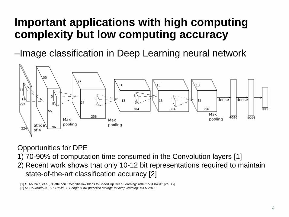
Important applications with high computing complexity but low computing accuracy–Image classification in Deep Learning neural network
4
Opportunities for DPE1) 70-90% of computation time consumed in the Convolution layers [1]2) Recent work shows that only 10-12 bit representations required to maintain
state-of-the-art classification accuracy [2][1] F. Abuzaid, et al., “Caffe con Troll: Shallow Ideas to Speed Up Deep Learning” arXiv:1504.04343 [cs.LG][2] M. Courbariaux, J.P. David, Y. Bengio “Low precision storage for deep learning” ICLR 2015
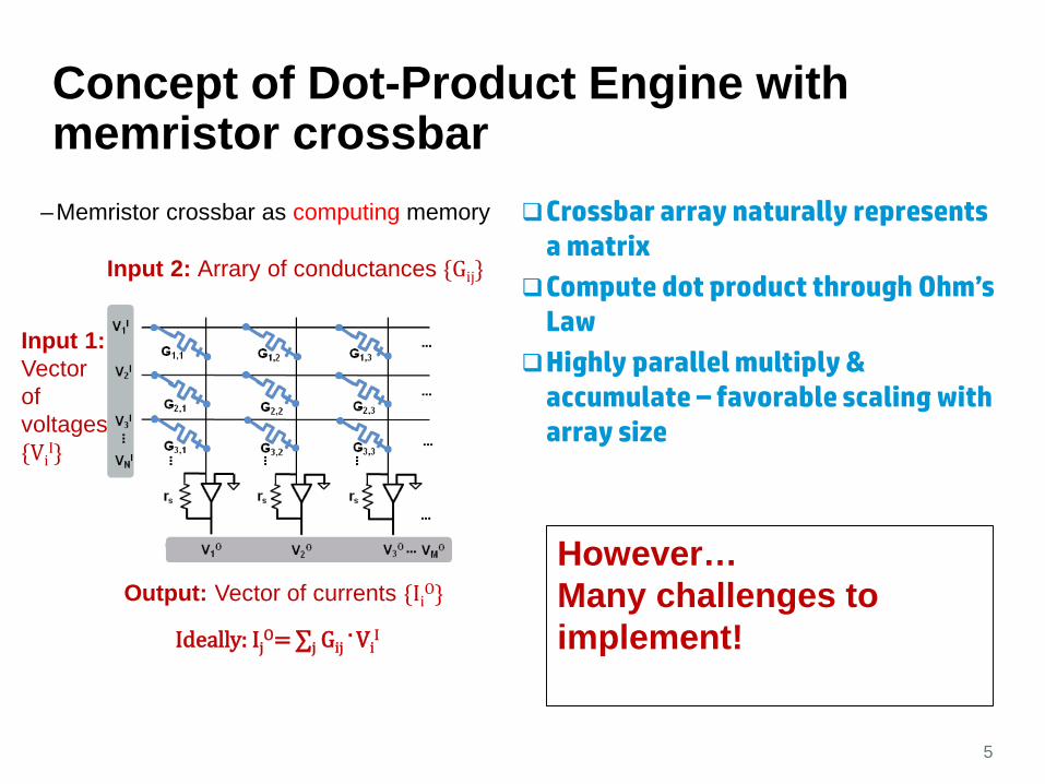
Concept of Dot-Product Engine with memristor crossbar
5
Input 2: Arrary of conductances Gij
Input 1:Vector of voltagesVi
I
Output: Vector of currents IiO
Ideally: IjO= ∑j Gij
. ViI
Crossbar array naturally represents a matrix
Compute dot product through Ohm’s Law
Highly parallel multiply & accumulate – favorable scaling with array size
However…Many challenges to implement!
–Memristor crossbar as computing memory
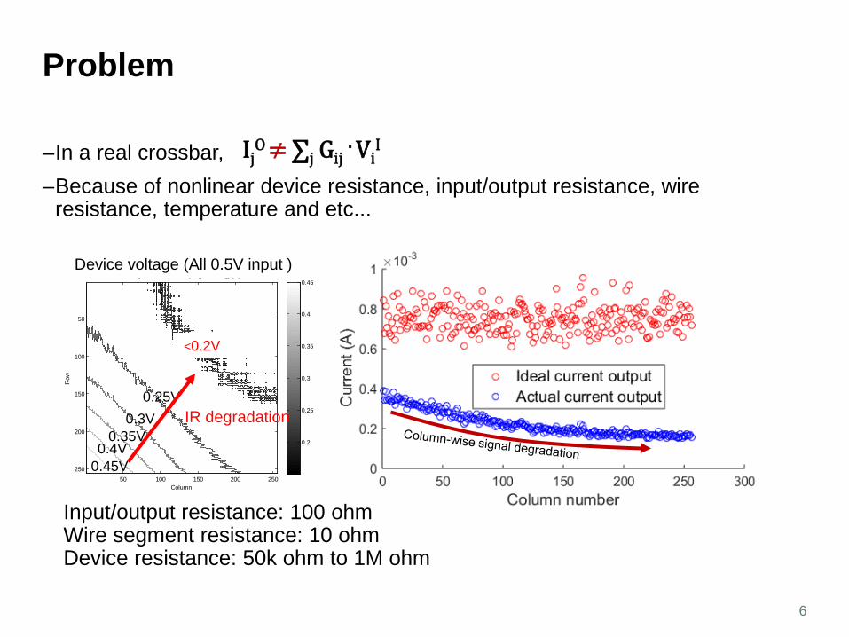
Problem
–In a real crossbar, –Because of nonlinear device resistance, input/output resistance, wire
resistance, temperature and etc...
6
IjO ≠ ∑j Gij
. ViI
Voltage across devices (single-biasing) (V)
Column
Row
50 100 150 200 250
50
100
150
200
250
0.2
0.25
0.3
0.35
0.4
0.45
Device voltage (All 0.5V input )
<0.2V
0.45V0.4V
0.35V0.3V
0.25VIR degradation
Input/output resistance: 100 ohmWire segment resistance: 10 ohm Device resistance: 50k ohm to 1M ohm
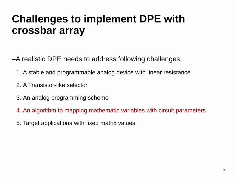
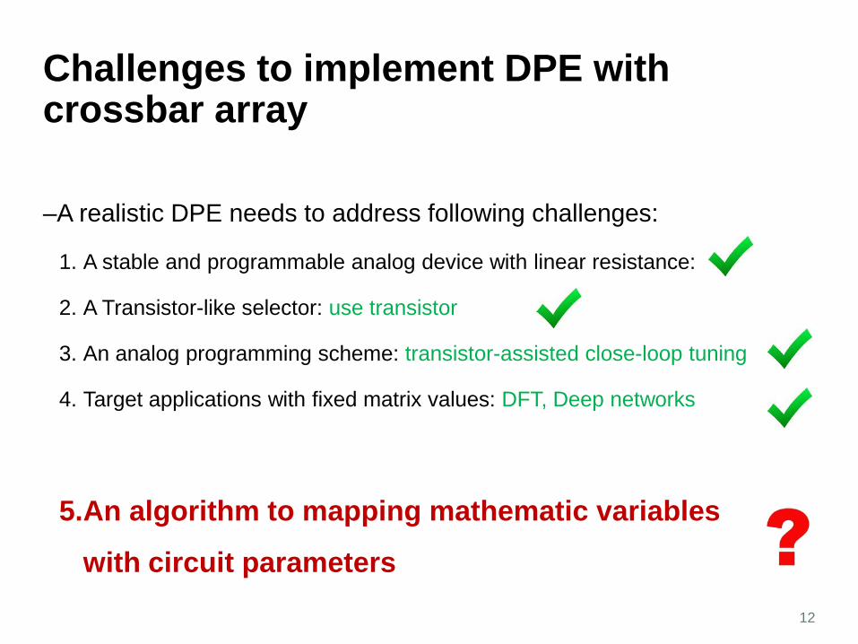
Challenges to implement DPE with crossbar array
–A realistic DPE needs to address following challenges:
1. A stable and programmable analog device with linear resistance
2. A Transistor-like selector
3. An analog programming scheme
4. An algorithm to mapping mathematic variables with circuit parameters
5. Target applications with fixed matrix values
7
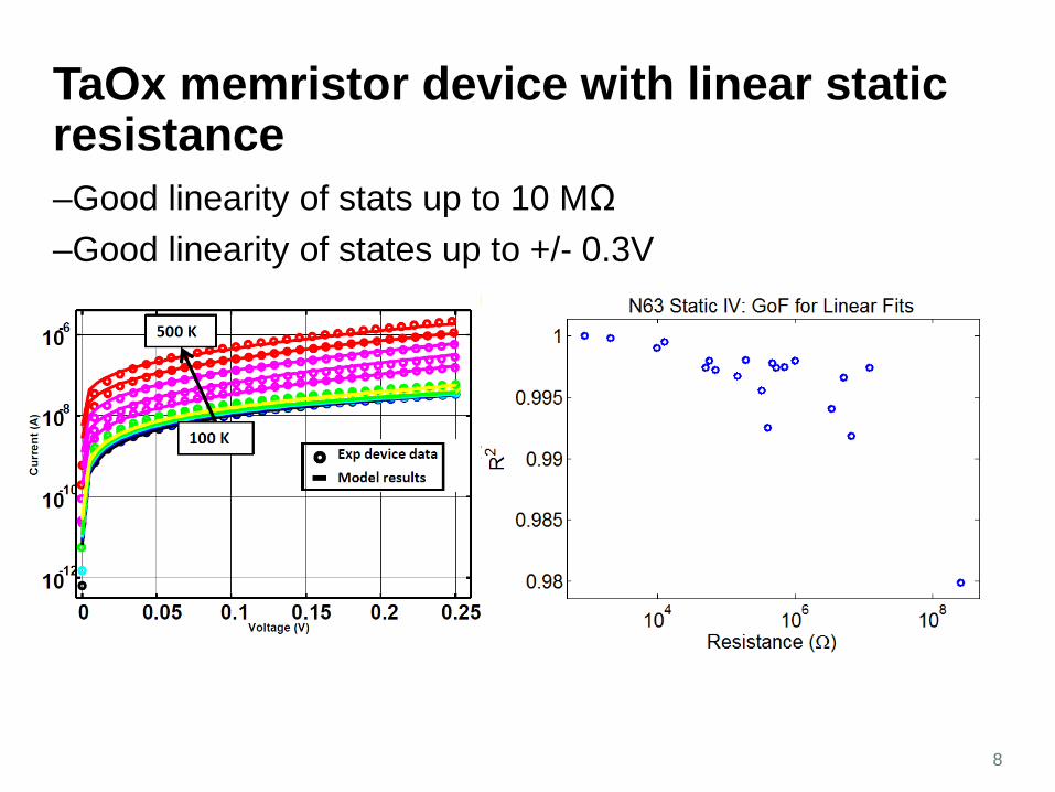
TaOx memristor device with linear static resistance–Good linearity of stats up to 10 MΩ–Good linearity of states up to +/- 0.3V
8
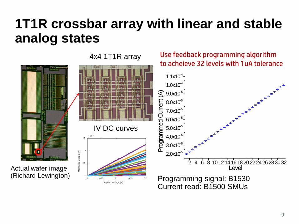
1T1R crossbar array with linear and stable analog states
9
Actual wafer image(Richard Lewington)
4x4 1T1R array
2 4 6 8 1012 1416 182022 2426 2830 322.0x10⁻⁵
3.0x10⁻⁵
4.0x10⁻⁵
5.0x10⁻⁵
6.0x10⁻⁵
7.0x10⁻⁵
8.0x10⁻⁵
9.0x10⁻⁵
1.0x10⁻⁴
1.1x10⁻⁴
LevelPr
ogra
mm
ed C
urre
nt (A
)
Use feedback programming algorithm to acheieve 32 levels with 1uA tolerance
Applied Voltage (V)
0 0.05 0.1 0.15 0.2
Mem
risto
r Cur
rent
(A)
10 -4
0
0.5
1
1.5
IV DC curves
Programming signal: B1530 Current read: B1500 SMUs
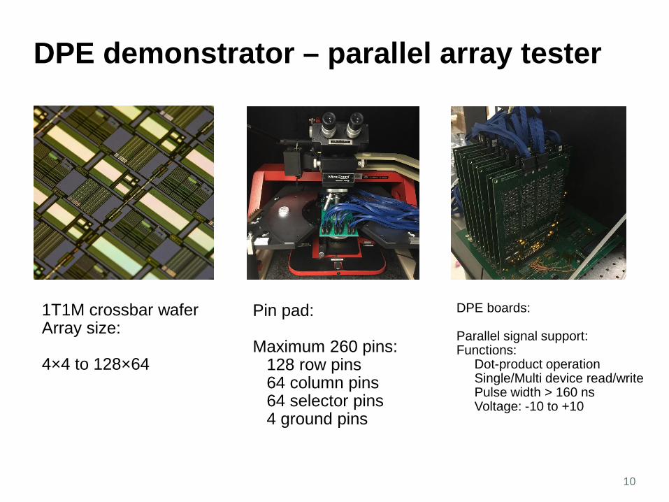
DPE demonstrator – parallel array tester
10
1T1M crossbar waferArray size:
4×4 to 128×64
Pin pad:
Maximum 260 pins: 128 row pins64 column pins 64 selector pins 4 ground pins
DPE boards:
Parallel signal support:Functions:
Dot-product operationSingle/Multi device read/writePulse width > 160 nsVoltage: -10 to +10

– - What is the status of achieving linear repeatable response, low power, sufficiently long retention, fast writes, sufficiently distinguishable resistances in different states, and long write endurance in one nanoscale device?
– - Is the access device issue solved? What are the remaining issues?
–For Dot-product Engine 1T1R devices: –Linear repeatable response: Good enough < 0.3V–Long retention: days and weeks, and it’s overall stable. –Fast writes: < 100 ns–Distinguishable resistances: 5~6 bits–Long write endurance: > 10^8 –Access device: transistor is the best solution so far.
–Problem of existing selectors for analog computing:–Variation & stability–Nonlinear ON state –Yield –Require high read voltage for computing
11
Summary of the 1T1R devices
Challenges to implement DPE with crossbar array
–A realistic DPE needs to address following challenges:
1. A stable and programmable analog device with linear resistance:
2. A Transistor-like selector: use transistor
3. An analog programming scheme: transistor-assisted close-loop tuning
4. Target applications with fixed matrix values: DFT, Deep networks
5.An algorithm to mapping mathematic variables
with circuit parameters
12
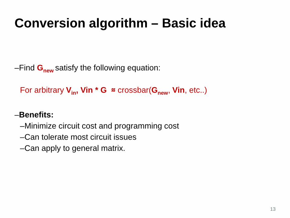
Conversion algorithm – Basic idea
–Find Gnew satisfy the following equation:
For arbitrary Vin, Vin * G ≈ crossbar(Gnew, Vin, etc..)
–Benefits: –Minimize circuit cost and programming cost–Can tolerate most circuit issues –Can apply to general matrix.
13
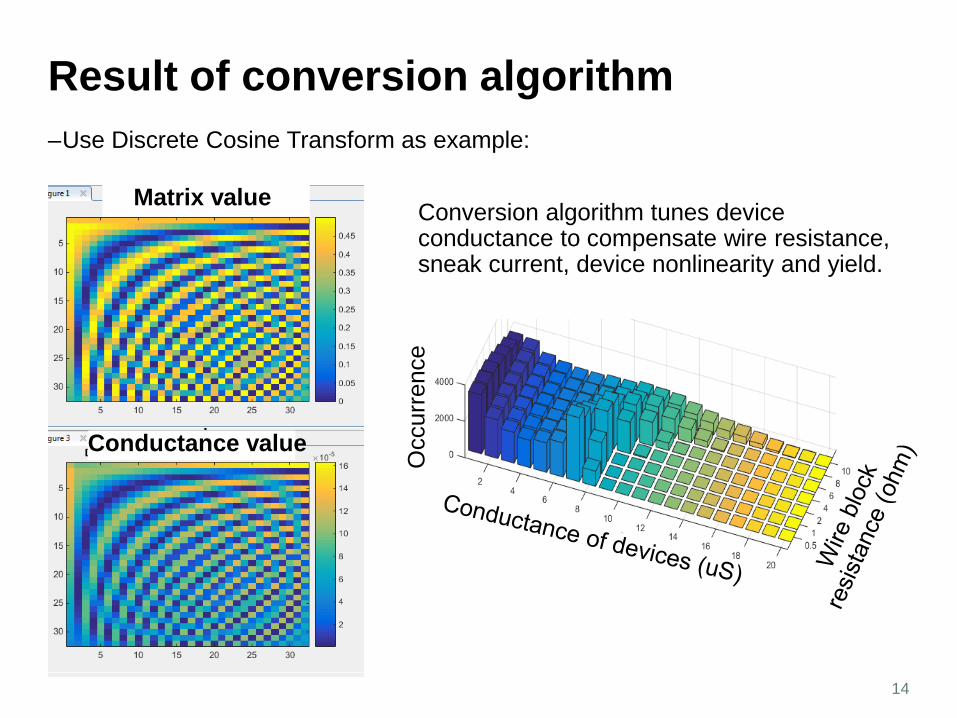
Result of conversion algorithm –Use Discrete Cosine Transform as example:
14
Matrix value
Conductance value O
ccur
renc
e
Conversion algorithm tunes device conductance to compensate wire resistance, sneak current, device nonlinearity and yield.
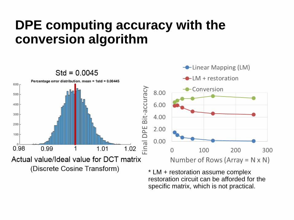
DPE computing accuracy with the conversion algorithm
* LM + restoration assume complex restoration circuit can be afforded for the specific matrix, which is not practical.
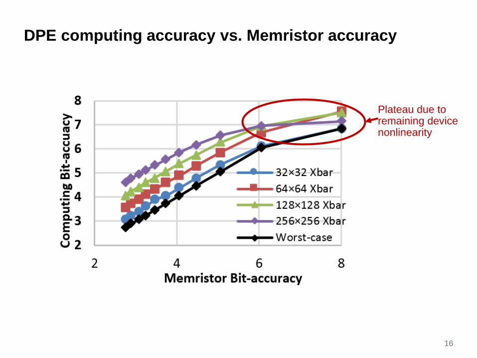
DPE computing accuracy vs. Memristor accuracy
16
Plateau due to remaining device nonlinearity
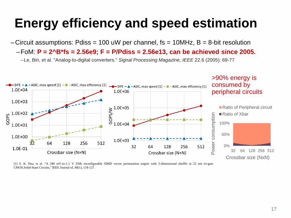
Energy efficiency and speed estimation–Circuit assumptions: Pdiss = 100 uW per channel, fs = 10MHz, B = 8-bit resolution
–FoM: P = 2^B*fs = 2.56e9; F = P/Pdiss = 2.56e13, can be achieved since 2005.–Le, Bin, et al. "Analog-to-digital converters." Signal Processing Magazine, IEEE 22.6 (2005): 69-77
17
[1] S. K. Hsu, et al. “A 280 mV-to-1.1 V 256b reconfigurable SIMD vector permutation engine with 2-dimensional shuffle in 22 nm tri-gateCMOS.Solid-State Circuits,” IEEE Journal of, 48(1), 118-127.
0%
50%
100%
32 64 128 256 512Pow
er c
onsu
mpt
ion
Crossbar size (NxN)
Ratio of Peripheral circuitRatio of Xbar
>90% energy is consumed by peripheral circuits
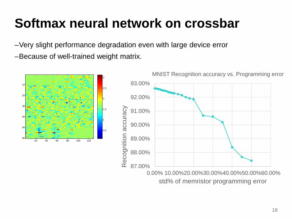
Softmax neural network on crossbar
18
87.00%
88.00%
89.00%
90.00%
91.00%
92.00%
93.00%
0.00% 10.00%20.00%30.00%40.00%50.00%60.00%
Rec
ogni
tion
accu
racy
std% of memristor programming error
MNIST Recognition accuracy vs. Programming error
–Very slight performance degradation even with large device error –Because of well-trained weight matrix.
20 40 60 80 100 120
10
20
30
40
50
60
0.5
1
1.5
2
2.5
3
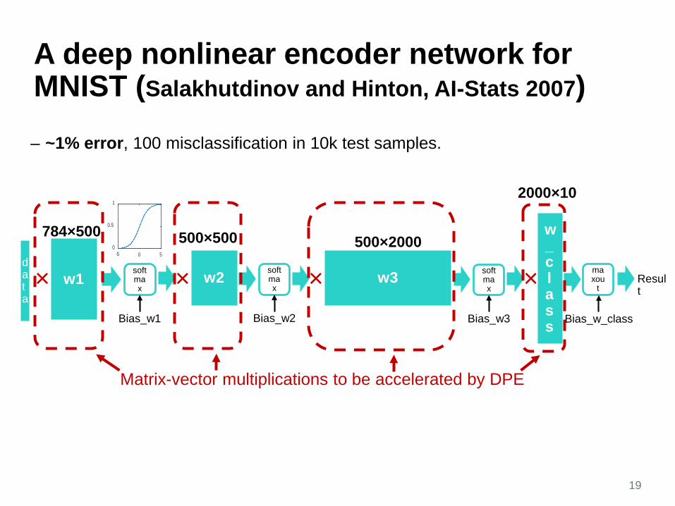
A deep nonlinear encoder network for MNIST (Salakhutdinov and Hinton, AI-Stats 2007)
19
– ~1% error, 100 misclassification in 10k test samples.
data
w1
784×500
× softmax
-5 0 50
0.5
1
Bias_w1
softmax
Bias_w2
w2
500×500
× softmax
Bias_w3
w3
500×2000
×
w_class
2000×10
× maxou
tResult
Bias_w_class
Matrix-vector multiplications to be accelerated by DPE
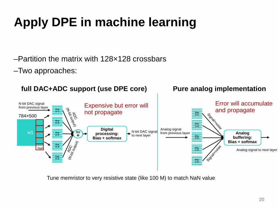
Apply DPE in machine learning
20
–Partition the matrix with 128×128 crossbars –Two approaches:
w1
784×500 Xbar(1,1)
Xbar(1,2)
Xbar(1,3)
Xbar(1,4)
Tune memristor to very resistive state (like 100 M) to match NaN value
Xbar(1,5)
NaN
full DAC+ADC support (use DPE core)
SUM
N-bit DAC signalto next layer
Digital processing:
Bias + softmax
N-bit DAC signal from previous layer
Pure analog implementation
Xbar(1,1)
Xbar(1,2)
Xbar(1,3)
Xbar(1,4)
Xbar(1,5)
Analog signal to next layer
Analog buffering:
Bias + softmax
Analog signal from previous layer
Error will accumulate and propagate
Expensive but error will not propagate
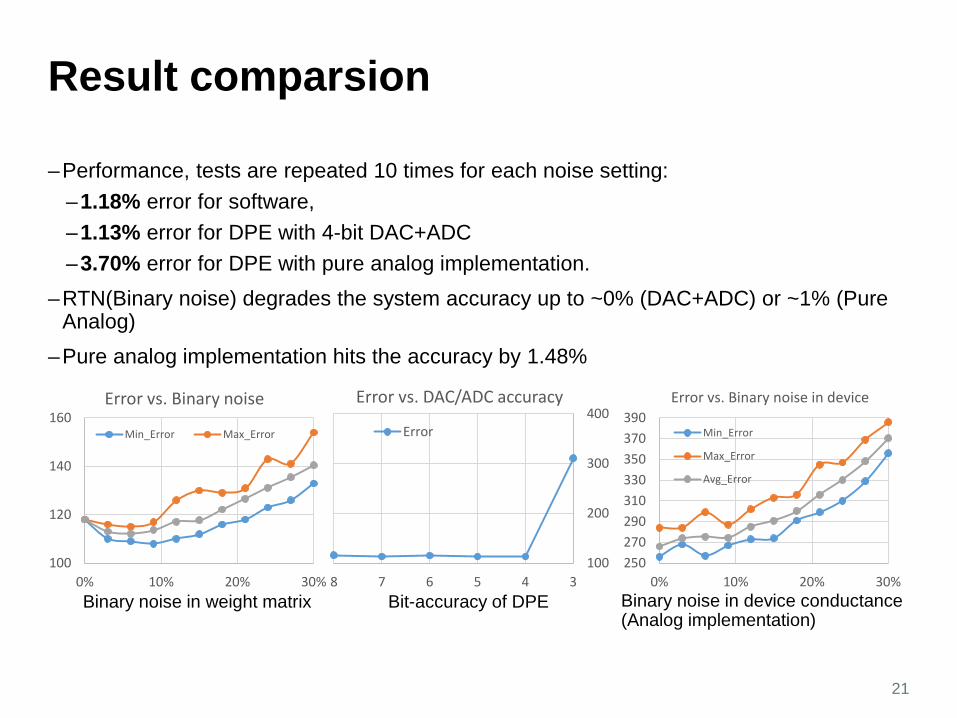
Result comparsion
21
–Performance, tests are repeated 10 times for each noise setting: –1.18% error for software, –1.13% error for DPE with 4-bit DAC+ADC–3.70% error for DPE with pure analog implementation.
–RTN(Binary noise) degrades the system accuracy up to ~0% (DAC+ADC) or ~1% (Pure Analog)
–Pure analog implementation hits the accuracy by 1.48%
100
120
140
160
0% 10% 20% 30%
Error vs. Binary noise
Min_Error Max_Error
250270290310330350370390
0% 10% 20% 30%
Error vs. Binary noise in device
Min_Error
Max_Error
Avg_Error
Binary noise in weight matrix Bit-accuracy of DPE Binary noise in device conductance(Analog implementation)
100
200
300
400
345678
Error vs. DAC/ADC accuracy
Error
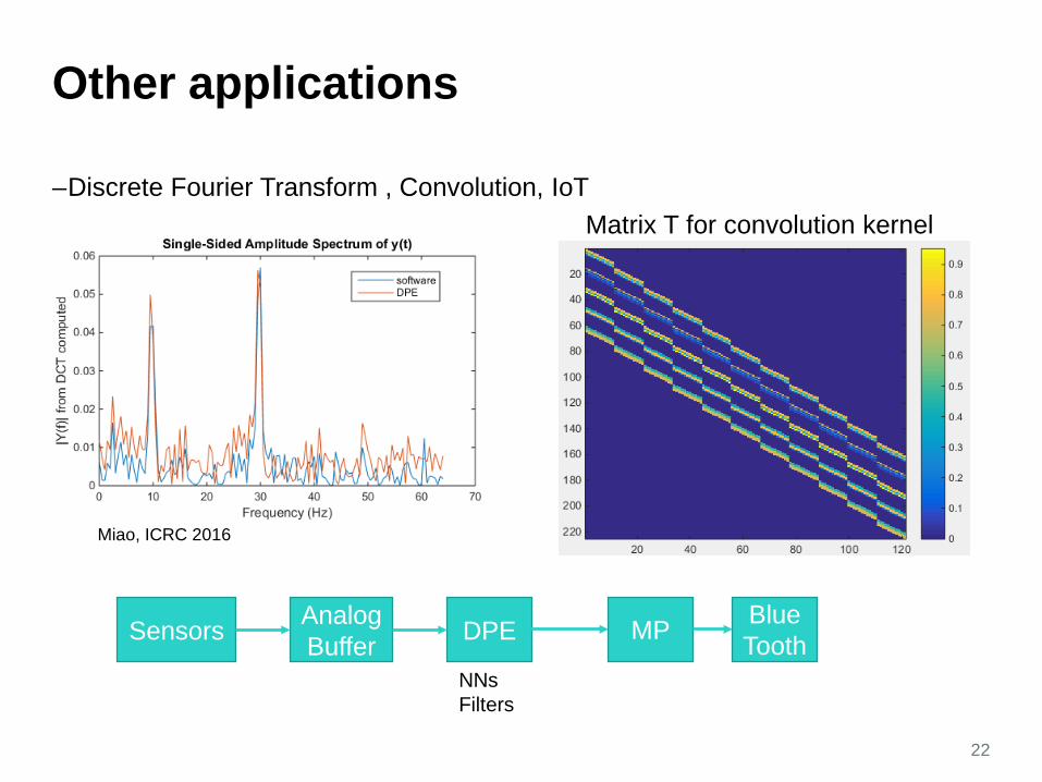
Other applications
–Discrete Fourier Transform , Convolution, IoT
22
DPE MPAnalog BufferSensors Blue
ToothNNsFilters
Matrix T for convolution kernel
Miao, ICRC 2016
Conclusion
–We analyzed the challenges for a practical Dot-Product Engine implementation on nano-crossbars
–We present a conversion algorithm with near-zero overhead: –Scalable up to 512x512 crossbar model or even more–Up to 8-Bit output accuracy–<2 second on a normal desktop workstation for 128x128 crossbar
–DPE is excellent as accelerators for off-line machine learning algorithms: –More than 3 orders of magnitude improvement comparing to the best possible ASIC
–1,000 to 10,000 better speed-energy efficiency product –Enough and flexible computing accuracy for trained NNs (no training yet)
23
24
Thank you!
For more detail please refer:
Miao et. al, “Dot-product engine for neuromorphic computing: programming 1T1M crossbar to accelerate matrix-vector multiplication,” DAC 2016.
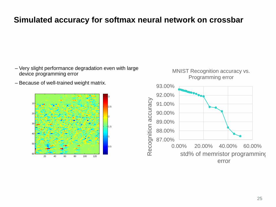
Simulated accuracy for softmax neural network on crossbar
25
87.00%88.00%89.00%90.00%91.00%92.00%93.00%
0.00% 20.00% 40.00% 60.00%R
ecog
nitio
n ac
cura
cystd% of memristor programming
error
MNIST Recognition accuracy vs. Programming error
– Very slight performance degradation even with large device programming error
– Because of well-trained weight matrix.
20 40 60 80 100 120
10
20
30
40
50
60
0.5
1
1.5
2
2.5
3
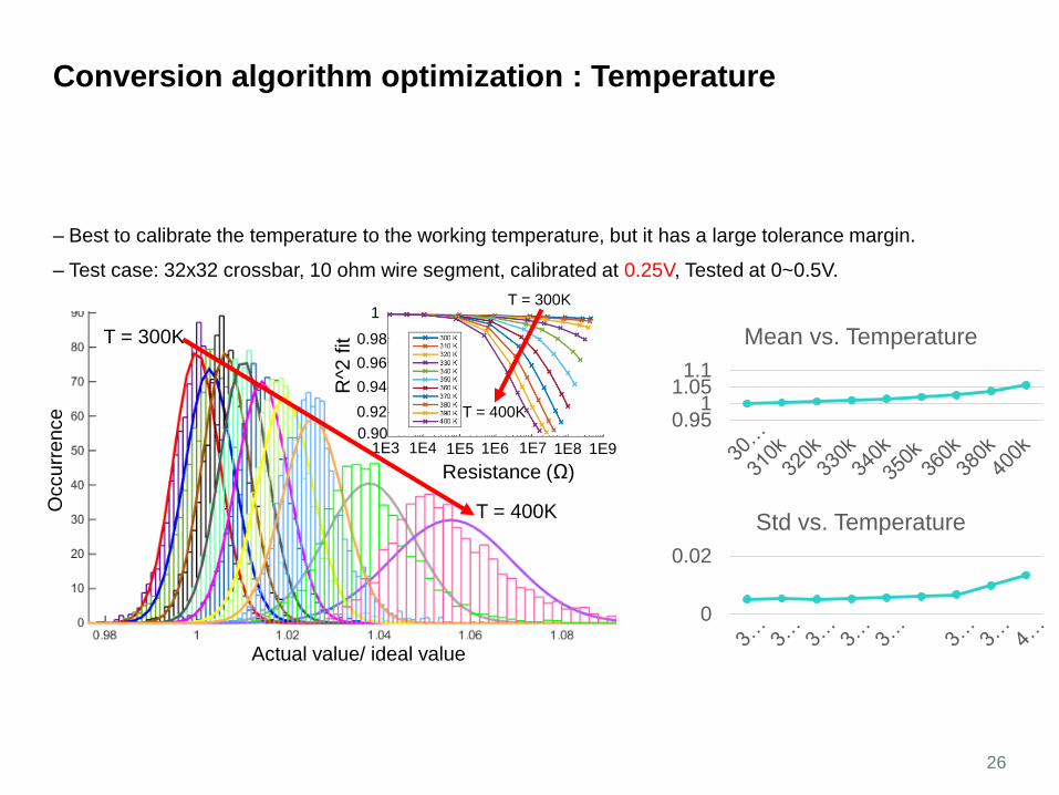
Conversion algorithm optimization : Temperature
26
– Best to calibrate the temperature to the working temperature, but it has a large tolerance margin.
– Test case: 32x32 crossbar, 10 ohm wire segment, calibrated at 0.25V, Tested at 0~0.5V.
Actual value/ ideal value
Occ
urre
nce
T = 300K
T = 400K
0.951
1.051.1
Mean vs. Temperature
0
0.02Std vs. Temperature
T = 300K
T = 400K
R^2
fit
1
0.980.960.940.920.90
Resistance (Ω)1E3 1E4 1E5 1E6 1E7 1E8 1E9
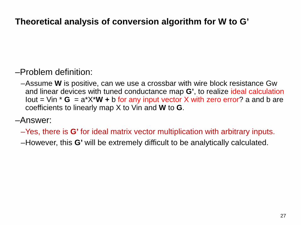
Theoretical analysis of conversion algorithm for W to G’
27
–Problem definition: –Assume W is positive, can we use a crossbar with wire block resistance Gw
and linear devices with tuned conductance map G’, to realize ideal calculationIout = Vin * G = a*X*W + b for any input vector X with zero error? a and b are coefficients to linearly map X to Vin and W to G.
–Answer: –Yes, there is G’ for ideal matrix vector multiplication with arbitrary inputs. –However, this G’ will be extremely difficult to be analytically calculated.
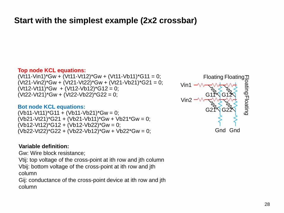
Start with the simplest example (2x2 crossbar)
28
G11
G21
G12
G22
Top node KCL equations: (Vt11-Vin1)*Gw + (Vt11-Vt12)*Gw + (Vt11-Vb11)*G11 = 0;(Vt21-Vin2)*Gw + (Vt21-Vt22)*Gw + (Vt21-Vb21)*G21 = 0;(Vt12-Vt11)*Gw + (Vt12-Vb12)*G12 = 0;(Vt22-Vt21)*Gw + (Vt22-Vb22)*G22 = 0;
Bot node KCL equations: (Vb11-Vt11)*G11 + (Vb11-Vb21)*Gw = 0;(Vb21-Vt21)*G21 + (Vb21-Vb11)*Gw + Vb21*Gw = 0;(Vb12-Vt12)*G12 + (Vb12-Vb22)*Gw = 0;(Vb22-Vt22)*G22 + (Vb22-Vb12)*Gw + Vb22*Gw = 0;
Vin1
Gnd Gnd
Vin2
Floating
Floating
Floating
Floating
Variable definition: Gw: Wire block resistance; Vtij: top voltage of the cross-point at ith row and jth columnVbij: bottom voltage of the cross-point at ith row and jthcolumnGij: conductance of the cross-point device at ith row and jthcolumn
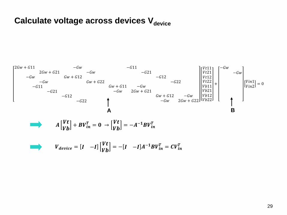
Calculate voltage across devices Vdevice
29
2𝐺𝐺𝐺𝐺 + 𝐺𝐺𝐺𝐺2𝐺𝐺𝐺𝐺 + 𝐺𝐺2𝐺
−𝐺𝐺𝐺𝐺−𝐺𝐺𝐺𝐺
−𝐺𝐺𝐺𝐺−𝐺𝐺𝐺𝐺
𝐺𝐺𝐺𝐺 + 𝐺𝐺𝐺2𝐺𝐺𝐺𝐺 + 𝐺𝐺22
−𝐺𝐺𝐺𝐺−𝐺𝐺2𝐺
−𝐺𝐺𝐺2−𝐺𝐺22
−𝐺𝐺𝐺𝐺−𝐺𝐺2𝐺
−𝐺𝐺𝐺2−𝐺𝐺22
𝐺𝐺𝐺𝐺 + 𝐺𝐺𝐺𝐺 −𝐺𝐺𝐺𝐺−𝐺𝐺𝐺𝐺 2𝐺𝐺𝐺𝐺 + 𝐺𝐺2𝐺
𝐺𝐺𝐺𝐺 + 𝐺𝐺𝐺2 −𝐺𝐺𝐺𝐺−𝐺𝐺𝐺𝐺 2𝐺𝐺𝐺𝐺 + 𝐺𝐺22
𝑉𝑉𝑡𝑡𝐺𝐺𝑉𝑉𝑡𝑡2𝐺𝑉𝑉𝑡𝑡𝐺2𝑉𝑉𝑡𝑡22𝑉𝑉𝑉𝑉𝐺𝐺𝑉𝑉𝑉𝑉2𝐺𝑉𝑉𝑉𝑉𝐺2𝑉𝑉𝑉𝑉22
+
−𝐺𝐺𝐺𝐺−𝐺𝐺𝐺𝐺
𝑉𝑉𝑖𝑖𝑖𝑖𝐺𝑉𝑉𝑖𝑖𝑖𝑖2 = 0
A B
𝑨𝑨 𝑽𝑽𝒕𝒕𝑽𝑽𝑽𝑽 + 𝑩𝑩𝑽𝑽𝒊𝒊𝒊𝒊
𝑻𝑻 = 𝟎𝟎 → 𝑽𝑽𝒕𝒕𝑽𝑽𝑽𝑽 = −𝑨𝑨−𝟏𝟏𝑩𝑩𝑽𝑽𝒊𝒊𝒊𝒊
𝑻𝑻
𝑽𝑽𝒅𝒅𝒅𝒅𝒅𝒅𝒊𝒊𝒅𝒅𝒅𝒅 = 𝑰𝑰 −𝑰𝑰 𝑽𝑽𝒕𝒕𝑽𝑽𝑽𝑽 = − 𝑰𝑰 −𝑰𝑰 𝑨𝑨−𝟏𝟏𝑩𝑩𝑽𝑽𝒊𝒊𝒊𝒊
𝑻𝑻 = 𝑪𝑪𝑽𝑽𝒊𝒊𝒊𝒊𝑻𝑻
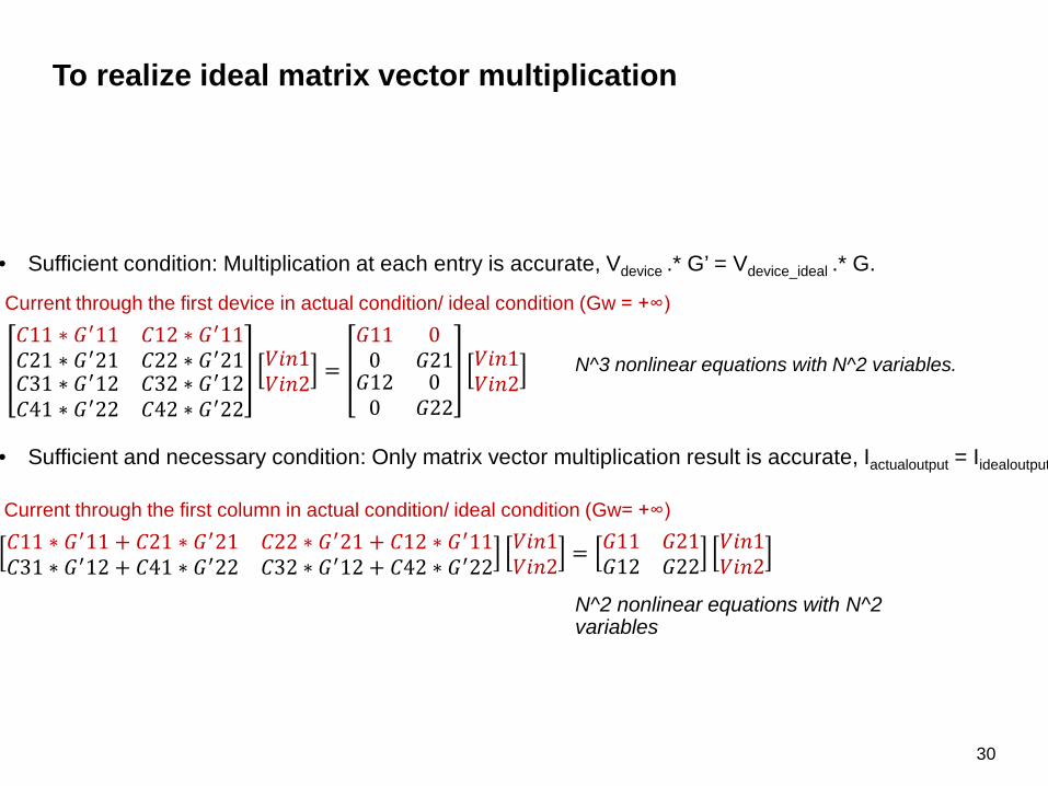
To realize ideal matrix vector multiplication
30
𝐶𝐶𝐺𝐺 ∗ 𝐺𝐺′𝐺𝐺 𝐶𝐶𝐺2 ∗ 𝐺𝐺′𝐺𝐺𝐶𝐶2𝐺 ∗ 𝐺𝐺′2𝐺 𝐶𝐶22 ∗ 𝐺𝐺′2𝐺𝐶𝐶3𝐺 ∗ 𝐺𝐺′𝐺2 𝐶𝐶32 ∗ 𝐺𝐺′𝐺2𝐶𝐶4𝐺 ∗ 𝐺𝐺′22 𝐶𝐶42 ∗ 𝐺𝐺′22
𝑉𝑉𝑖𝑖𝑖𝑖𝐺𝑉𝑉𝑖𝑖𝑖𝑖2 =
𝐺𝐺𝐺𝐺0
0𝐺𝐺2𝐺
𝐺𝐺𝐺20
0𝐺𝐺22
𝑉𝑉𝑖𝑖𝑖𝑖𝐺𝑉𝑉𝑖𝑖𝑖𝑖2
• Sufficient condition: Multiplication at each entry is accurate, Vdevice .* G’ = Vdevice_ideal .* G.
N^3 nonlinear equations with N^2 variables.
𝐶𝐶𝐺𝐺 ∗ 𝐺𝐺′𝐺𝐺 + 𝐶𝐶2𝐺 ∗ 𝐺𝐺′2𝐺 𝐶𝐶22 ∗ 𝐺𝐺′2𝐺 + 𝐶𝐶𝐺2 ∗ 𝐺𝐺′𝐺𝐺𝐶𝐶3𝐺 ∗ 𝐺𝐺′𝐺2 + 𝐶𝐶4𝐺 ∗ 𝐺𝐺′22 𝐶𝐶32 ∗ 𝐺𝐺′𝐺2 + 𝐶𝐶42 ∗ 𝐺𝐺′22
𝑉𝑉𝑖𝑖𝑖𝑖𝐺𝑉𝑉𝑖𝑖𝑖𝑖2 = 𝐺𝐺𝐺𝐺 𝐺𝐺2𝐺
𝐺𝐺𝐺2 𝐺𝐺22𝑉𝑉𝑖𝑖𝑖𝑖𝐺𝑉𝑉𝑖𝑖𝑖𝑖2
• Sufficient and necessary condition: Only matrix vector multiplication result is accurate, Iactualoutput = Iidealoutput
N^2 nonlinear equations with N^2 variables
Current through the first device in actual condition/ ideal condition (Gw = +∞)
Current through the first column in actual condition/ ideal condition (Gw= +∞)
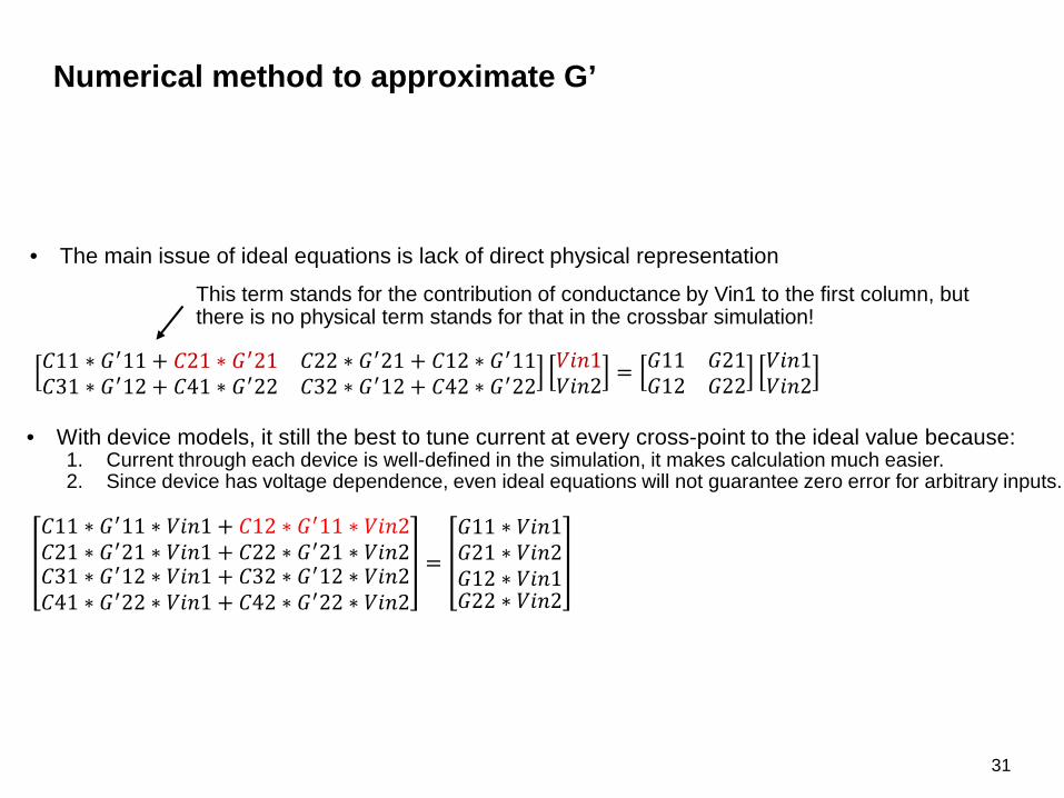
Numerical method to approximate G’
31
𝐶𝐶𝐺𝐺 ∗ 𝐺𝐺′𝐺𝐺 + 𝐶𝐶2𝐺 ∗ 𝐺𝐺′2𝐺 𝐶𝐶22 ∗ 𝐺𝐺′2𝐺 + 𝐶𝐶𝐺2 ∗ 𝐺𝐺′𝐺𝐺𝐶𝐶3𝐺 ∗ 𝐺𝐺′𝐺2 + 𝐶𝐶4𝐺 ∗ 𝐺𝐺′22 𝐶𝐶32 ∗ 𝐺𝐺′𝐺2 + 𝐶𝐶42 ∗ 𝐺𝐺′22
𝑉𝑉𝑖𝑖𝑖𝑖𝐺𝑉𝑉𝑖𝑖𝑖𝑖2 = 𝐺𝐺𝐺𝐺 𝐺𝐺2𝐺
𝐺𝐺𝐺2 𝐺𝐺22𝑉𝑉𝑖𝑖𝑖𝑖𝐺𝑉𝑉𝑖𝑖𝑖𝑖2
• The main issue of ideal equations is lack of direct physical representation
This term stands for the contribution of conductance by Vin1 to the first column, but there is no physical term stands for that in the crossbar simulation!
• With device models, it still the best to tune current at every cross-point to the ideal value because: 1. Current through each device is well-defined in the simulation, it makes calculation much easier. 2. Since device has voltage dependence, even ideal equations will not guarantee zero error for arbitrary inputs.
𝐶𝐶𝐺𝐺 ∗ 𝐺𝐺′𝐺𝐺 ∗ 𝑉𝑉𝑖𝑖𝑖𝑖𝐺 + 𝐶𝐶𝐺2 ∗ 𝐺𝐺′𝐺𝐺 ∗ 𝑉𝑉𝑖𝑖𝑖𝑖2𝐶𝐶2𝐺 ∗ 𝐺𝐺′2𝐺 ∗ 𝑉𝑉𝑖𝑖𝑖𝑖𝐺 + 𝐶𝐶22 ∗ 𝐺𝐺′2𝐺 ∗ 𝑉𝑉𝑖𝑖𝑖𝑖2𝐶𝐶3𝐺 ∗ 𝐺𝐺′𝐺2 ∗ 𝑉𝑉𝑖𝑖𝑖𝑖𝐺 + 𝐶𝐶32 ∗ 𝐺𝐺′𝐺2 ∗ 𝑉𝑉𝑖𝑖𝑖𝑖2𝐶𝐶4𝐺 ∗ 𝐺𝐺′22 ∗ 𝑉𝑉𝑖𝑖𝑖𝑖𝐺 + 𝐶𝐶42 ∗ 𝐺𝐺′22 ∗ 𝑉𝑉𝑖𝑖𝑖𝑖2
=𝐺𝐺𝐺𝐺 ∗ 𝑉𝑉𝑖𝑖𝑖𝑖𝐺𝐺𝐺2𝐺 ∗ 𝑉𝑉𝑖𝑖𝑖𝑖2𝐺𝐺𝐺2 ∗ 𝑉𝑉𝑖𝑖𝑖𝑖𝐺𝐺𝐺22 ∗ 𝑉𝑉𝑖𝑖𝑖𝑖2


![Particle Swarm Optimization Algorithm in Calibration of ...in the navigation solution [1]. To compensate the drift errors, others sensors are used in the navigation algorithm, such](https://static.fdocuments.in/doc/165x107/5f90a1004577d91e0d228be6/particle-swarm-optimization-algorithm-in-calibration-of-in-the-navigation-solution.jpg)