Using an external LO Source with the Octagon PLL Low Noise Block … · Using an external LO Source...
4
Using an external LO Source with the Octagon PLL Low Noise Block Andy Talbot G4JNT 2016-06-30 The Octagon Phase Locked LNB offers a stable low noise figure front end suitable for narrow band operation on 10GHz. Its LO has low close in phase noise making it suitable for narrow band digital data modes like JT4. Some measurements on its performance can be found at http://www.g4jnt.com/pll_lnb_tests.pdf However, in is raw form, the LO is derived from a free running crystal which drifts several kHz or even tens of kHz with temperature variations. The solution is to use an external high stability frequency reference The crystal supplied runs at 27MHz and is internally multiplied by 361.111 ( = 3250/9) to give an LO at 9750MHz. This means 10368MHz input comes out at 618MHz. The crystal can be removed and a high stability external input at 27MHz can be supplied instead. Modifying for External LO Reference Photo 1 by M0EYT shows his original Octagon innards with its 27MHz crystal. There are actually two completely independent LOs within the casing, one lies on the lower side, opposite to two F-type connectors, and shown in Photo 1, but there is another LNB under the smaller cover on the other side, adjacent to the connectors. Either or both sides can be modified, but here only the one on the lower side is done. Remove the five 6- point star head screws (all M2.5 size) holding the lid, after scraping away the sealant that covers the screw heads. Prise off the lid to reveal the innards of Photo 1.
Transcript of Using an external LO Source with the Octagon PLL Low Noise Block … · Using an external LO Source...

Using an external LO Source with the Octagon PLL Low Noise Block
Andy Talbot G4JNT 2016-06-30
The Octagon Phase Locked LNB offers a stable low noise figure front end suitable for narrow band
operation on 10GHz. Its LO has low close in phase noise making it suitable for narrow band digital data
modes like JT4. Some measurements on its performance can be found at
http://www.g4jnt.com/pll_lnb_tests.pdf
However, in is raw form, the LO is derived from a free running crystal which drifts several kHz or even tens
of kHz with temperature variations. The solution is to use an external high stability frequency reference
The crystal supplied runs at 27MHz and is internally multiplied by 361.111 ( = 3250/9) to give an LO at
9750MHz. This means 10368MHz input comes out at 618MHz. The crystal can be removed and a high
stability external input at 27MHz can be supplied instead.
Modifying for External LO Reference
Photo 1 by M0EYT shows
his original Octagon innards
with its 27MHz crystal.
There are actually two
completely independent
LOs within the casing, one
lies on the lower side,
opposite to two F-type
connectors, and shown in
Photo 1, but there is another LNB under the smaller cover on the other side, adjacent to the connectors.
Either or both sides can be modified, but here only the one on the lower side is done. Remove the five 6-
point star head screws (all M2.5 size) holding the lid, after scraping away the sealant that covers the screw
heads. Prise off the lid to reveal the innards of Photo 1.

Photo 2 shows the modifications needed, with the missing PCB pads where the crystal sat being clearly
visible. By trial and error it was determined which of the two crystal connections was the input to the
oscillator (Murphy failed here and I got the right connections the first time). A DC blocking capacitor
passes external 27MHz RF to the PLL, and a termination resistor to ground is added to provide some input
matching. 0604 sized components needs to be used here as 0805 types are just a bit too unwieldy .
Scrape away the resist
on the ground plane to
secure the braid of thin
PTFE coax; connect the
inner to the termination
resistor / DC block
junction. Photo 3 shows
the modification in more
detail.
[Note: the termination
resistor value of 62Ω as
that is all I had in 0604
size]
Case Modification
To allow the reference cable to pass though to the outside world, cut and file a slot in the edge of the
cover as shown in Photo 4, at the point where the LO reference cable passes off the PCB. Make sure it is
below the gold plated bit
adjacent to the connections
to the other F-Type
connector (belonging to the
alternate LNB module),
shown top right of Photo 2.
There is a web on the cover,
visible in Photo 4, that
presses down onto the gold-
plated area to give some
screening from the main
PCB.
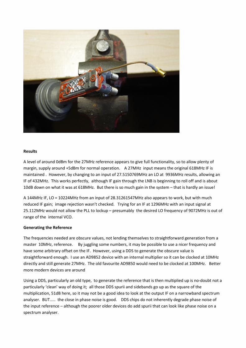
The reassembled LNB can be
seen in Photo 5
Results
A level of around 0dBm for the 27MHz reference appears to give full functionality, so to allow plenty of
margin, supply around +5dBm for normal operation. A 27MHz input means the original 618MHz IF is
maintained . However, by changing to an input of 27.5150769MHz an LO at 9936MHz results, allowing an
IF of 432MHz. This works perfectly, although IF gain through the LNB is beginning to roll off and is about
10dB down on what it was at 618MHz. But there is so much gain in the system – that is hardly an issue!
A 144MHz IF, LO = 10224MHz from an input of 28.31261547MHz also appears to work, but with much
reduced IF gain; image rejection wasn’t checked. Trying for an IF at 1296MHz with an input signal at
25.112MHz would not allow the PLL to lockup – presumably the desired LO frequency of 9072MHz is out of
range of the internal VCO.
Generating the Reference
The frequencies needed are obscure values, not lending themselves to straightforward generation from a
master 10MHz, reference. By juggling some numbers, it may be possible to use a nicer frequency and
have some arbitrary offset on the IF. However, using a DDS to generate the obscure value is
straightforward enough. I use an AD9852 device with an internal multiplier so it can be clocked at 10MHz
directly and still generate 27MHz. The old favourite AD9850 would need to be clocked at 100MHz. Better
more modern devices are around
Using a DDS, particularly an old type, to generate the reference that is then multiplied up is no-doubt not a
particularly ‘clean’ way of doing it; all those DDS spurii and sidebands go up as the square of the
multiplication, 51dB here, so it may not be a good idea to look at the output IF on a narrowband spectrum
analyser. BUT..... the close in phase noise is good. DDS chips do not inherently degrade phase noise of
the input reference – although the poorer older devices do add spurii that can look like phase noise on a
spectrum analyser.
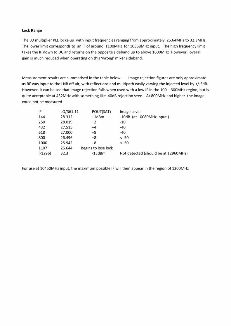
Lock Range
The LO multiplier PLL locks-up with input frequencies ranging from approximately 25.64MHz to 32.3MHz.
The lower limit corresponds to an IF of around 1100MHz for 10368MHz input. The high frequency limit
takes the IF down to DC and returns on the opposite sideband up to above 1600MHz However, overall
gain is much reduced when operating on this ‘wrong’ mixer sideband.
Measurement results are summarised in the table below. Image rejection figures are only approximate
as RF was input to the LNB off air, with reflections and multipath easily varying the injected level by +/-5dB.
However, it can be see that image rejection falls when used with a low IF in the 100 – 300MHz region, but is
quite acceptable at 432MHz with something like 40dB rejection seen. At 800MHz and higher the image
could not be measured
IF LO/361.11 POUT(SAT) Image Level
144 28.312 +1dBm -10dB (at 10080MHz input )
250 28.019 +2 -10
432 27.515 +4 -40
618 27.000 +8 -40
800 26.496 +8 < -50
1000 25.942 +8 < -50
1107 25.644 Begins to lose lock
(-1296) 32.3 -15dBm Not detected (should be at 12960MHz)
For use at 10450MHz input, the maximum possible IF will then appear in the region of 1200MHz