
Using ADS to Ensure Signal Integrity on Multi-Gigabit ... 1 Ludwig Eichinger Agilent EEsof EDA Using...
45
Page 1 Ludwig Eichinger Agilent EEsof EDA Using ADS to Ensure Signal Integrity on Multi-Gigabit Serial Links ADS Seminar Nov/Dec 2009
Transcript of Using ADS to Ensure Signal Integrity on Multi-Gigabit ... 1 Ludwig Eichinger Agilent EEsof EDA Using...

Page 1
Ludwig Eichinger
Agilent EEsof EDA
Using ADS to Ensure
Signal Integrity on
Multi-Gigabit Serial Links
ADS Seminar Nov/Dec 2009

Page 2
Agenda: Signal Integrity Simulations Using
Advanced Design System
• Introduction
• Concept – System Design – Verification
• Channel Simulation Technologies and Methods
• Cannel Modeling in Frequency Domain
• Integration and Verification
• Demo and Advanced Design Techniques

Page 3
Typical SI Problem ( Ensuring Signal Quality and Timing)
Pattern
Generator
Pre-emphasis/Driver
Encoder
Decoder
Receiver
Equalizer
Physic
al C
hannel
Board Traces 2” (51mm) – 10” (254mm)
Card
Card
Package
Die
Package
Die Driver
Receiver
Card
High speed Connectors
Backplane Traces
10” (254mm) –
40” (1016mm)
Physic
al C
hannel
Channel Adaptation
Signal Recovery
IBIS or Spice model
IBIS or Spice model

Page 4
Signal Degradation• Low pass filter characteristic of transmission line (attenuates high
frequency component in a signal which results in smearing out sharp
edges)
• Radiation, dispersion, resonance, and frequency dependent losses
of transmission lines degrades wave shape
• Interference caused by cross talk ( coupling between adjacent
transmission lines) and EMI degrades wave shape
• Impedance mismatch due to transmission line discontinuities
• High frequency parasitic, delays, and asymmetric transmission path
• Through Hole Vias
Basic microwave problem

Why ADS?
Improve Performance of your Communication System
Page 5

Page 6
How ADS can help to overcome SI Effects?
Better control of impedance, mismatch & discontinuities in the transmission path
• Better isolation between transmission lines reduces cross talk
• Tight control of power and ground plane impedance
Signal processing techniques to reduce signal distortion ( ISI)
• Pre-emphasis (Transmitter side)• Boost high frequency components in a digital signal to compensate for low pass filtering effects of transmission lines
• Equalization (Receive side) CTE , FFE, DFE
• Boost high frequency components in a digital signal to compensate low pass filtering effects of transmission lines and dispersion effects
• Controlled attenuation of low frequency component to make frequency domain response flat over the frequency and dispersion effects
Simulation of extremely low BER.
Account for different types of jitter: ISI, DCD, PJ & RJ
Tx and Rx equalizers
Effects of crosstalk channels
Page 7
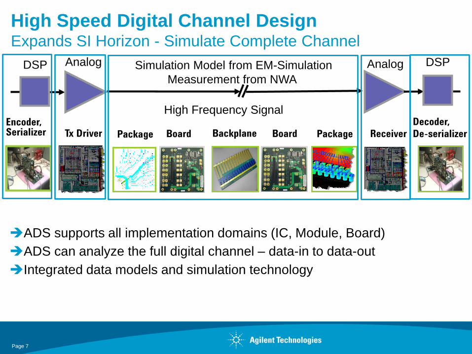
Tx Driver BoardPackage Backplane
ADS supports all implementation domains (IC, Module, Board)
ADS can analyze the full digital channel – data-in to data-out
Integrated data models and simulation technology
High Speed Digital Channel DesignExpands SI Horizon - Simulate Complete Channel
BoardEncoder, Serializer
Decoder,
De-serializerPackage Receiver
DSP DSPAnalog Simulation Model from EM-Simulation
Measurement from NWA
Analog
High Frequency Signal

Fast Channel Modeling
Page 8

Page 9
Tx Driver
Channel Source - Differential or Single Ended
Bit Rate
Vlow/Vhigh
Rise/Fall Time
Register Length (i.e. 2^19)
Encoder (8B10B)
Preemphasis
De-Deemphasis
Jitter
DCD, RJ, PJAmplitude, PJFrequency
Fast Channel Modeling – Source Tx
Encoder, Serializer
DSP Analog
ADS Channel Source

Page 10
Fast Channel Simulation – Rx
Decoder,
De-serializerReceiver
DSPAnalog
Support three type of equalizations
Continous-time linear equalizer (CTE): pole-zero
Feed-forword equalizer (FFE)
Decison-feedback equalizer (DFE)
Optimize the initial taps automatically with innovative algorithm
Accept user specified taps through dialogue or tap file
Adapt taps with LMS, RLS or ZF algorithm during the simulation
Save the optimized taps on file
Account for RJ
Page 11
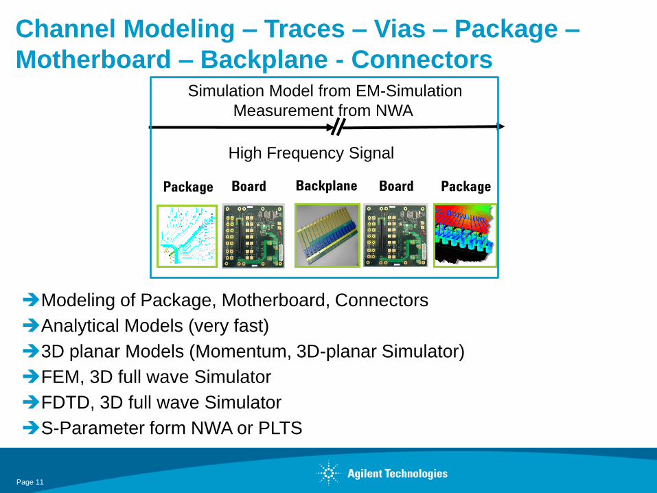
BoardPackage Backplane
Modeling of Package, Motherboard, Connectors
Analytical Models (very fast)
3D planar Models (Momentum, 3D-planar Simulator)
FEM, 3D full wave Simulator
FDTD, 3D full wave Simulator
S-Parameter form NWA or PLTS
Channel Modeling – Traces – Vias – Package –
Motherboard – Backplane - Connectors
Board Package
Simulation Model from EM-Simulation
Measurement from NWA
High Frequency Signal
Page 12
Fast Channel Modeling :Parameterized
Transmission Line Models

Page 13
Fast Channel Channel Modeling:
Flexible Representation of Interconnects
S-parameters
Inbuilt Multilayer Interconnect library
W-element
Physical models (EM)
Measurement based
Rational Polynomials
Pole zero
Lumped representation (Broadband SPICE)

Page 14
Eye diagram
S-parameters
from VNA
FFT
HDMI cable (7 meters):
Measured (pink) and simulated
(blue) response correspond exactly
Fast Channel Modeling:
Data Based Model from a Network Analyzer

Fast Channel Simulation
Page 15

Fast Eye Measurements - User Interface
The Eye probes will be available from Transient and Channel Simulator Palette.The Eye probes is available from Transient and Channel Simulator Palette.
Page 16

Fast Eye Measurements - User Interface
Page 17

Fast Eye Mask Definition
Page 18
Use Model
1. Browse for the mask file* from the Eye Probe dialog.
2. Activate the Eye Mask Viewer dialog by clicking on the
View/Edit button from the Eye Probe
3. The contents of the mask file should be plotted for
verification prior to simulation.
4. Click on the Edit button to edit the contents of the mask
file. The refresh button can be used to update the mask
plot.
1
2 4
3

Eye Mask Display
Page 19
The simulator will save the Eye
Mask for each Eye Probe.
In addition if the user requests for
mask violation checks to be
performed, the simulator will
check for violations and report
using 1 or 0 in the variable named
“MaskViolated”.

How to improve the Channel Quality?
•Channel Simulation, includes Traces, Vias, Connectors, Package, etc.
• Simulation Methods
• TDR/TDT
•Mixed Mode S-Parameters
•Cross Talk Analysis
TDR Simulation
Mixed Mode S-Parameter
Page 20

Identify the Problem
88.7 Ohm88.7 Ohm
Page 21

Step 1: Design of input and output Matching
NetworksSource Impedance is 100 Ohm
Impedance of the Package at input and output is 88.7 Ohm
Solution Design of a Matching Network
Smith Chart UtilityS11dd
mismatch
Page 22

Step 2: Fast Channel Optimization
Optimization of the intermediate traces (w, s) and de-emphasis in the Source
Matching Network
Matching Network
Optimizer
Page 23
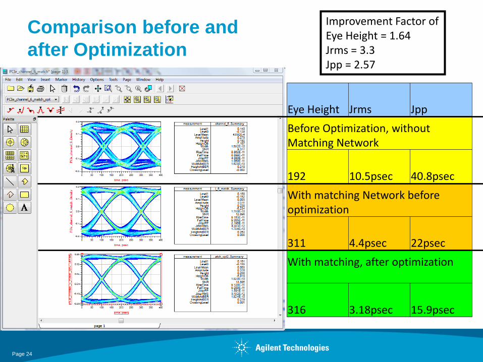
Comparison before and
after Optimization
Eye Height Jrms Jpp
Before Optimization, without Matching Network
192 10.5psec 40.8psec
With matching Network before optimization
311 4.4psec 22psec
With matching, after optimization
316 3.18psec 15.9psec
Improvement Factor ofEye Height = 1.64Jrms = 3.3Jpp = 2.57
Page 24

Fast Channel Statistical Analysis
Page 25

Fast Channel Simulation - Cross Talk Analysis
Degradation Factorthrough Cross TalkEye Height = 1.05 lessJrms = 1.3 moreJpp = 1.3 moreWith Cross Talk
Without Cross Talk
Page 26

Channel Verification
Page 27

Page 28
Tx Driver
Channel Verification – Source Tx
Encoder, Serializer
DSP Analog • Inbuilt transistor models
• HSPICE netlist
• Spectre netlists
• Verilog-A
• Verilog-D cosim
• Verilog-AMS cosim
• Verilog/VHDL cosim
• MATLAB cosim
• C/C++/SystemC
• IBIS buffers
• IBIS AMI
• ADS Design Kit from Altera,
Xilinx, etc.

Page 29
Design Verification: Design Flow Integration
with Other EDA Tools
Allegro®
Expedition®
ADS/Momentum
BBSPICE
HSPICE/PSPICE
Allegro® import
Expedition® import
Broadband SPICE
Import critical nets from Cadence
Allegro or Mentor Expedition
environment to ADS for Momentum
simulation
Export Momentum results to
HSPICE
Links ADS and Momentum to external tools
Page 30
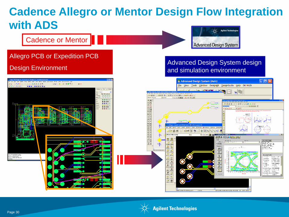
Cadence Allegro or Mentor Design Flow Integration
with ADS
Allegro PCB or Expedition PCB
Design Environment Advanced Design System design
and simulation environment
Cadence or Mentor

Channel Modeling: 3D EM tools from
Agilent
• The ONLY company with ALL 3 EM technologies
• Momentum (Method of Moments) 3D Planar
• EMDS (Finite Element Method) Full 3D In ADS and EMPro
• EMPro (Finite Difference Time Domain) Full 3D
Page 31

Page 32
EM Based Models:
Momentum- 3-D Planar EM SimulationFrequency domain analysis of arbitrary shaped geometry
• Via hole
• Planar Package and board
• Transitions and launch
• Connectors
• Arbitrary shaped transmission
lines and discontinuity
• SI and PI analysis

EM Based Models: EMPro 3D Full Wave EM - FEM
and FDTD
•3D Package
•High Speed Connectors
• SATA, HDMI, PCI
express, USB3,
SAS2, XAUI
•Conformal High Speed
Flex Circuits
Simulated Data
•S-Parameter
•Electric fields
•Multi-Mode Data
Page 33

Fast Channel Simulation - Layout Co-Simulation
Package Model
Package Model
Add in Card
Here we are performing EM co-simulation on the
add in card traces
Page 34

Package Co-simulation
Layout
Component
Page 35

Simulation, Post Processing and Data
RepresentationAutomated measurements
• Eye diagram
• Jitter analysis
• TDR/TDT
• Mixed Mode (Diff/Com)
Links with Test and
Measurement Instruments
• Essential for measurement-
based modeling
Bathtub/BER analysis
ADS model created from
TDR response
Page 36

Equalization Rx (FFE, DFE)
Optimize the initial taps automatically with innovative algorithm
Accept user specified taps through dialogue or tap file
Adapt taps with LMS, RLS or ZF algorithm
during the simulation
Save the optimized taps on file
Support three type of equalizations
Continous-time linear equalizer (CTE): pole-zero
Feed-forword equalizer (FFE)
Decison-feedback equalizer (DFE)
Page 37

Equalization Rx (FFE, DFE)
Results
With EqualizationWithout Equalization
Page 38

PCI Express Channel with Stratix-II GX Driver
Page 39

Design Guides, Tools …..
Page 40

Page 41
Broadband SPICE Model Generator
Input File Format
• ADS dataset
• Citifile format
• Touchstone file format
• Momentum RAT
Output Netlist Format
• ADS
• SPICE2
• SPICE3
Fast and Efficient way to convert S-parameter
models to their SPICE equivalent
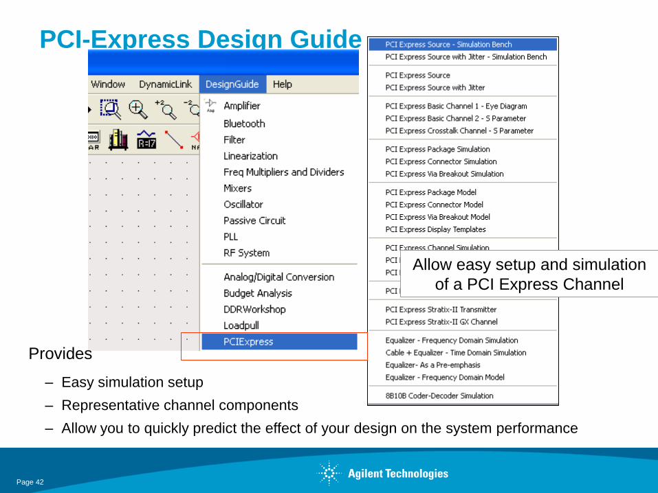
PCI-Express Design Guide
Allow easy setup and simulation
of a PCI Express Channel
Provides
– Easy simulation setup
– Representative channel components
– Allow you to quickly predict the effect of your design on the system performance
Page 42
More Design Guides
PCIe
DDR2
DDR3
USB
HDMI
These Design Guides needs to be installed in
Main Window/DesignGuide/Add DesignGuide
Navigate to $HPSSOSF_DIR\examples\ KC_examples and select PCI_Express etc.
Other Examples
Signal Integrity Applications (In the Design Guide Menu)
Examples in $HPSSOSF_DIR\examples\ SignalIntegrity
http://www.agilent.com/find/eesof click on Signal Integrity and then on
Quick Start for Signal Integrity Design Using Agilent ADS
Page 43

Summary - ADS Usage
• Compute the geometry of the differential traces on and between the layers to
achieve the desired differential Impedance
• Channel Simulation, including Vias, Connectors, Package
• Simulation Methods
• TDR/TDT
• Cross Talk Analysis
• Mixed Mode S-Parameters
• Eye, Jitter, BER, Statistics, Cross Talk
• Comparison with measurement
• De-embedding techniques is ADS
• Design Improvements
• Matching Networks
• Optimization of Analog circuit
• System Simulation including Analog Cannel and DSP circuits
•Optimization of Analog and DSP circuit
• Equalization Techniques (LFE, DFE, Blind DFE, etc.)
• Pre-, De-emphasis
Page 44

Page 45
– SPICE tools are not sufficient to model high speed Serial
Link Channel
– Designer requires accurate time domain simulation of S-
parameters (ADS provides far superior time-domain
simulation technology)
– Designer needs to integrate DSP components such as
SERDES, Pre-emphasis and Equalization. ( ADS provide
industry best co-simulation technology and can simulate a
channel containing a combination of Analog, DSP, MATLAB,
EM, C++, and HDL components)
– Jitter analysis is very important for success of the product
– Accurate analysis of BER is important for 1st pass success.
Summary