User's Guide - Texas Instruments · surprise. 4.3 Program and Debug the Temperature Measurement...
24
LAUNCHXL-F28069M Overview User's Guide Literature Number: SPRUI11 January 2015
Transcript of User's Guide - Texas Instruments · surprise. 4.3 Program and Debug the Temperature Measurement...

LAUNCHXL-F28069M Overview
User's Guide
Literature Number: SPRUI11January 2015

Contents
1 Introduction......................................................................................................................... 42 Kit Contents ........................................................................................................................ 53 Installation .......................................................................................................................... 5
3.1 Energia .................................................................................................................... 53.2 Code Composer Studio ................................................................................................. 5
4 Getting Started with the LAUNCHXL-F28069M ......................................................................... 64.1 Getting Started ........................................................................................................... 64.2 Demo Application, Internal Temperature Measurement ............................................................ 64.3 Program and Debug the Temperature Measurement Demo Application ......................................... 6
5 Hardware Configuration ........................................................................................................ 65.1 Power Domain ............................................................................................................ 75.2 Serial Connectivity ....................................................................................................... 75.3 Boot Mode Selection..................................................................................................... 75.4 Connecting a Crystal..................................................................................................... 75.5 Connecting a BoosterPack.............................................................................................. 85.6 Device Migration Path ................................................................................................... 8
6 LAUNCHXL-F28069M Hardware ............................................................................................. 96.1 Device Pin Out............................................................................................................ 96.2 Schematics .............................................................................................................. 116.3 PCB Layout.............................................................................................................. 186.4 Bill of Materials (BOM) ................................................................................................. 19
7 References ........................................................................................................................ 228 Frequently Asked Questions (FAQ) ...................................................................................... 23
2 Table of Contents SPRUI11–January 2015Submit Documentation Feedback
Copyright © 2015, Texas Instruments Incorporated

www.ti.com
List of Figures1 LAUNCHXL-F28069M Board Overview................................................................................... 52 LAUNCHXL-F28069_B_1400922 Block Diagram Schematic ........................................................ 113 LAUNCHXL-F28069_B_1400922 USB to JTAG Schematic.......................................................... 124 LAUNCHXL-F28069_B_1400922 F28069_A Schematic ............................................................. 135 LAUNCHXL-F28069_B_1400922 F28069_B Schematic ............................................................. 146 LAUNCHXL-F28069_B_1400922 Connector Schematic ............................................................. 157 LAUNCHXL-F28069_B_1400922 Logic Choice Schematic .......................................................... 168 LAUNCHXL-F28069_B_1400922 Power Schematic .................................................................. 179 Top Silk ...................................................................................................................... 1810 Top Copper ................................................................................................................. 1811 Inner Copper 1.............................................................................................................. 1812 Inner Copper 2.............................................................................................................. 1813 Bottom Silk .................................................................................................................. 1814 Bottom Copper.............................................................................................................. 18
List of Tables1 Serial Connectivity ........................................................................................................... 72 F28069M LaunchPad Pin Out and Pin Mux Options - J1, J3.......................................................... 93 F28069M LaunchPad Pin Out and Pin Mux Options - J4, J2.......................................................... 94 F28069M LaunchPad Pin Out and Pin Mux Options - J5, J7 ........................................................ 105 F28069M LaunchPad Pin Out and Pin Mux Options - J8, J6 ........................................................ 106 LAUNCHXL-F28069M Bill of Materials .................................................................................. 19
3SPRUI11–January 2015 List of FiguresSubmit Documentation Feedback
Copyright © 2015, Texas Instruments Incorporated
User's GuideSPRUI11–January 2015
LAUNCHXL-F28069M Overview
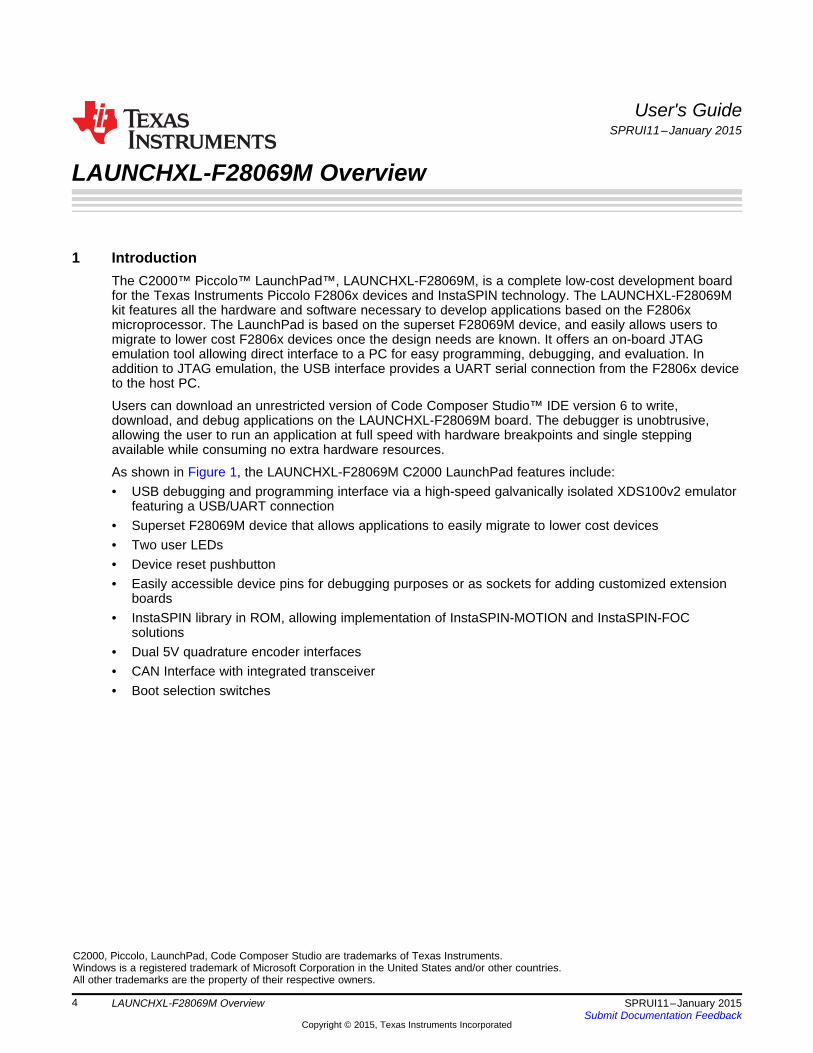
1 IntroductionThe C2000™ Piccolo™ LaunchPad™, LAUNCHXL-F28069M, is a complete low-cost development boardfor the Texas Instruments Piccolo F2806x devices and InstaSPIN technology. The LAUNCHXL-F28069Mkit features all the hardware and software necessary to develop applications based on the F2806xmicroprocessor. The LaunchPad is based on the superset F28069M device, and easily allows users tomigrate to lower cost F2806x devices once the design needs are known. It offers an on-board JTAGemulation tool allowing direct interface to a PC for easy programming, debugging, and evaluation. Inaddition to JTAG emulation, the USB interface provides a UART serial connection from the F2806x deviceto the host PC.
Users can download an unrestricted version of Code Composer Studio™ IDE version 6 to write,download, and debug applications on the LAUNCHXL-F28069M board. The debugger is unobtrusive,allowing the user to run an application at full speed with hardware breakpoints and single steppingavailable while consuming no extra hardware resources.
As shown in Figure 1, the LAUNCHXL-F28069M C2000 LaunchPad features include:• USB debugging and programming interface via a high-speed galvanically isolated XDS100v2 emulator
featuring a USB/UART connection• Superset F28069M device that allows applications to easily migrate to lower cost devices• Two user LEDs• Device reset pushbutton• Easily accessible device pins for debugging purposes or as sockets for adding customized extension
boards• InstaSPIN library in ROM, allowing implementation of InstaSPIN-MOTION and InstaSPIN-FOC
solutions• Dual 5V quadrature encoder interfaces• CAN Interface with integrated transceiver• Boot selection switches
C2000, Piccolo, LaunchPad, Code Composer Studio are trademarks of Texas Instruments.Windows is a registered trademark of Microsoft Corporation in the United States and/or other countries.All other trademarks are the property of their respective owners.
4 LAUNCHXL-F28069M Overview SPRUI11–January 2015Submit Documentation Feedback
Copyright © 2015, Texas Instruments Incorporated

www.ti.com Kit Contents
Figure 1. LAUNCHXL-F28069M Board Overview
2 Kit ContentsThe LAUNCHXL-F28069M LaunchPad experimenter kit includes the following items:• C2000 LaunchPad Board (LAUNCHXL-F28069M)• Mini USB-B Cable, 0.5m• Quick Start Guide
3 InstallationThe F28069M LaunchPad is supported in both Code Composer Studio and Energia. Depending on yourtools preference you may wish to install one or the other or both.
3.1 EnergiaGo to Energia.nu and and click on the Guide tab. Click on the link for your operating system and follow thedirections to install Energia.
3.2 Code Composer Studio
3.2.1 Download the Required SoftwareCode Composer Studio IDE is available for free without any restriction when used with the XDS100emulator on the C2000 LaunchPad. The software can be downloaded from the C2000 LaunchPad page atti.com/launchpad. At this site, you can also download a copy of controlSUITE that includes drivers,examples, and other support software needed to get started.
For InstaSPIN motor control projects, install the latest version of MotorWare.exe (www.ti.com/motorware)and run MotorWare.exe. In the window that opens, under Resources, follow the Kit Readme and GUIQuick Start Guide for the LAUNCHXL-F28069M.
5SPRUI11–January 2015 LAUNCHXL-F28069M OverviewSubmit Documentation Feedback
Copyright © 2015, Texas Instruments Incorporated

Getting Started with the LAUNCHXL-F28069M www.ti.com
3.2.2 Install the SoftwareOnce downloaded, install Code Composer Studio and the controlSUITE package.
3.2.3 Install the HardwareAfter Code Composer Studio is installed, plug the supplied USB cable into the C2000 LaunchPad boardand into an available USB port on your computer.
Windows® will automatically detect the hardware and ask you to install software drivers. Let Windows runa search for the drivers and automatically install them. After Windows successfully installs the drivers forthe integrated XDS100v2 emulator, your LaunchPad is now ready for use.
4 Getting Started with the LAUNCHXL-F28069M
4.1 Getting StartedThe first time the LAUNCHXL-F28069M is used, a demo application automatically starts when the board ispowered from a USB host. If your board does not start the demo application, try placing S1 in the followingpositions and resetting the board: UP - UP - DOWN. To start the demo, connect the LAUNCHXL-F28069M with the included mini-USB cable to a free USB port. The demo application starts with the LEDsflashing to show the device is active.
4.2 Demo Application, Internal Temperature MeasurementThe LAUNCHXL-F28069M includes a pre-programmed TMS320F28069M device. When the LaunchPad isconnected via USB, the demo starts with an LED flash sequence. After a few seconds the device switchesinto a temperature measurement mode.
A reference temperature is taken at the beginning of this mode and the LEDs of the LaunchPad are usedto display any difference between the current temperature and the reference temperature. If the devicegets warmer than the reference temperature the red LED is lit with an intensity proportional to thetemperature difference. However if the device cools down compared to the reference temperature, a blueLED is lit in the same fashion.
In addition to the LED display, temperature information is also displayed on your PC through theUSB/UART connection. To view the UART information on your PC, first figure out the COM portassociated with the LaunchPad. To do this in Windows, right click on My Computer and click onProperties. In the dialog box that appears, click on the Hardware tab and open Device Manager. Look foran entry under Ports (COM & LPT) titled "USB Serial Port (COMX)", where X is a number. Remember thisnumber for when you open a serial terminal. The demo applications UART data was written and debuggedusing PuTTY, and for the best user experience we recommend you use PuTTY to view the UART data.PuTTY can be downloaded from the following URL:
http://www.chiark.greenend.org.uk/~sgtatham/putty/download.html
Open your serial terminal program and open the COM port you found previously in device manager withthe following settings: 115200 Baud, 8 data bits, no parity, 1 stop bit. After opening the serial port in yourserial terminal, reset the Launchpad with the reset push button and observe the serial terminal for asurprise.
4.3 Program and Debug the Temperature Measurement Demo ApplicationThe project and associated source code for the C2000 Piccolo LaunchPad demo is included in thecontrolSUITE software package and should automatically be found by the TI Resource Explorer in CodeComposer Studio v6. In the resource explorer, open the controlSUITE folder and then the DevelopmentTools entry and look for the C2000 LaunchPad line item. Expand this item and LAUNCHXL-F28069M,then select the LaunchPad Demo Application. Follow the steps in the main pane of the resource explorerto import, build, debug, and run this application.
5 Hardware ConfigurationThe F28069M LaunchPad gives users several options as to how to configure the board.
6 LAUNCHXL-F28069M Overview SPRUI11–January 2015Submit Documentation Feedback
Copyright © 2015, Texas Instruments Incorporated
www.ti.com Hardware Configuration
5.1 Power DomainThe F28069M LaunchPad has several different power domains to enable JTAG isolation. Jumpers JP1,JP2, JP3, JP4, and JP5 configure where power is passed.
Jumper Power DomainJP1 Enable 3.3 V from USB (disables isolation)JP2 Enable GND from USB (disables isolation)JP3 Enable 5 V switcher (powered off 3.3 V supply of target device)JP4 Connects target MCU 3.3 V to second set of BoosterPack
headersJP5 Connects target MCU 5 V to second set of BoosterPack headers
5.2 Serial ConnectivityThe LAUNCHXL-F28069M has a USB to UART adapter built in. This makes it easy to print debuginformation back to the host PC even in isolated environments. The F28069M device on this LaunchPadcontains two SCI (UART) peripherals, while the LaunchPad has three places these peripherals need to berouted. Because of this, a serial connectivity mux has been added to the board to make configuration ofthe SCI routing easy. Routing is configured via two jumpers (JP6 and JP7). Configure the jumpers asshown in Table 1 for the serial connectivity you desire.
Table 1. Serial Connectivity
MUX_SEL CH_SEL(JP(JP7) 6) FunctionON ON USB/UART Disabled; J1.3 and J1.4 – GPIO28 and GPIO29; J7.3 and J7.4 – GPIO15 and GPIO58ON OFF USB/UART – GPIO28 and GPIO29, J1.3 and J1.4 – Hi-Z; J7.3 and J7.4 – GPIO15 and GPIO58OFF ON USB/UART – GPIO15 and GPIO58; FAULT/OCTW – GPIO28 and GPIO29; J7.3 and J7.4 – Hi-ZOFF OFF USB/UART – GPIO15 and GPIO58; FAULT/OCTW – GPIO28 and GPIO29; J7.3 and J7.4 – Hi-Z
5.3 Boot Mode SelectionThe LaunchPad's F28069M device includes a boot ROM that performs some basic start-up checks andallows for the device to boot in many different ways. Most users will either want to perform an emulationboot or a boot to flash (if they are running the application standalone). S1 has been provided to allowusers to easily configure the pins that the bootROM checks to make this decision. The switches on S1correspond to:
Switch Function1 GPIO342 GPIO373 TRSTn
Keep in mind that the debugger does not connect if the device is not in the emulation boot mode (TRSTswitch in the up position). More information about boot mode selection can be found in the Boot ROMsection of the TMS320x2806x Piccolo Technical Reference Guide (SPRUH18).
5.4 Connecting a CrystalAlthough the Piccolo device present on the LAUNCHXL-F28069M has an internal oscillator — and formost applications this is sufficient — the LaunchPad offers a footprint for through-hole HC-49 crystals forusers who require a more precise clock. If you wish to use an external crystal, solder the crystal to the Q1footprint and appropriate load capacitors to the C3 and C4 footprints. You also need to configure thedevice to use the external oscillator in software.
7SPRUI11–January 2015 LAUNCHXL-F28069M OverviewSubmit Documentation Feedback
Copyright © 2015, Texas Instruments Incorporated

Hardware Configuration www.ti.com
5.5 Connecting a BoosterPackThe F28069M LaunchPad is the perfect experimenter board to start hardware development with theF2806x devices. All of the connectors are aligned in a 0.1-in (2.54-mm) grid to allow easy and inexpensivedevelopment of add on boards called BoosterPacks. These satellite boards can access all of the GPIOand analog signals. The the pin out of the connectors can be found in Section 5.
5.6 Device Migration PathApplications developed on the LAUNCHXL-F28069M can easily be migrated to any of these lower costdevices in the F2806x family:
Part Number DescriptionTMS320F28069 32-Bit Real Time Microcontroller, 90 MHz, 256KB Flash, 100KB RAMTMS320F28069F 32-Bit Real Time Microcontroller, 90 MHz, 256KB Flash, 96KB RAMTMS320F28069M 32-Bit Real Time Microcontroller, 90 MHz, 256KB Flash, 96KB RAMTMS320F28068 32-Bit Real Time Microcontroller, 90 MHz, 256KB Flash, 100KB RAMTMS320F28068F 32-Bit Real Time Microcontroller, 90 MHz, 256KB Flash, 96KB RAMTMS320F28068M 32-Bit Real Time Microcontroller, 90 MHz, 256KB Flash, 96KB RAMTMS320F28067 32-Bit Real Time Microcontroller, 90 MHz, 256KB Flash, 100KB RAMTMS320F28066 32-Bit Real Time Microcontroller, 90 MHz, 256KB Flash, 68KB RAMTMS320F28065 32-Bit Real Time Microcontroller, 90 MHz, 128KB Flash, 100KB RAMTMS320F28064 32-Bit Real Time Microcontroller, 90 MHz, 128KB Flash, 100KB RAMTMS320F28063 32-Bit Real Time Microcontroller, 90 MHz, 128KB Flash, 100KB RAMTMS320F28062 32-Bit Real Time Microcontroller, 90 MHz, 128KB Flash, 52KB RAMTMS320F28062F 32-Bit Real Time Microcontroller, 90 MHz, 128KB Flash, 52KB RAM
8 LAUNCHXL-F28069M Overview SPRUI11–January 2015Submit Documentation Feedback
Copyright © 2015, Texas Instruments Incorporated

www.ti.com LAUNCHXL-F28069M Hardware
6 LAUNCHXL-F28069M Hardware
6.1 Device Pin Out
Table 2 through Table 5 lists the pin out and pin mux options for the C2000 LaunchPad.
Table 2. F28069M LaunchPad Pin Out and Pin Mux Options - J1, J3
Mux Value Mux Value3 2 1 0 J1 Pin J3 Pin 0 1 2 3
+3.3V 1 21 +5VADCINA6 2 22 GNDJ1.3 3 23 ADCINA7J1.4 4 24 ADCINB1
SPISIMOB SCITXDA TZ1 GPIO12 5 25 ADCINA2ADCINB6 6 26 ADCINB2
XCLKOUT SCITXDB SPICLKA GPIO18 7 27 ADCINA0SCITXDB MCLKXA EQEP1S GPIO22 8 28 ADCINB0ADCSOCBO EPWMSYNCO SCLA GPIO33 9 29 ADCINA1ADCSOCAO EWPMSYNCI SDAA GPIO32 10 30 NC
Table 3. F28069M LaunchPad Pin Out and Pin Mux Options - J4, J2
Mux Value Mux Value3 2 1 0 J4 Pin J2 Pin 0 1 2 3
Rsvd Rsvd EPWM1A GPIO0 40 20 GNDCOMP1OUT Rsvd EPWM1B GPIO1 39 19 GPIO19 SPISTEA SCIRXDB ECAP1Rsvd Rsvd EPWM2A GPIO2 38 18 GPIO44 MFSRA SCIRXDB EPWM7BCOMP2OUT SPISOMIA EPWM2B GPIO3 37 17 NCRsvd Rsvd EPWM3A GPIO4 36 16 RESET#ECAP1 SPISIMOA EPWM3B GPIO5 35 15 GPIO16 SPISIMOA Rsvd TZ2SPISOMIB Rsvd TZ2 GPIO13 34 14 GPIO17 SPISOMIA Rsvd TZ3
NC 33 13 GPIO50 EQEP1A MDXA TZ1DAC1 32 12 GPIO51 EQEP1B MDRA TZ2DAC2 31 11 GPIO55 SPISOMIA EQEP2A HRCAP1
9SPRUI11–January 2015 LAUNCHXL-F28069M OverviewSubmit Documentation Feedback
Copyright © 2015, Texas Instruments Incorporated
LAUNCHXL-F28069M Hardware www.ti.com
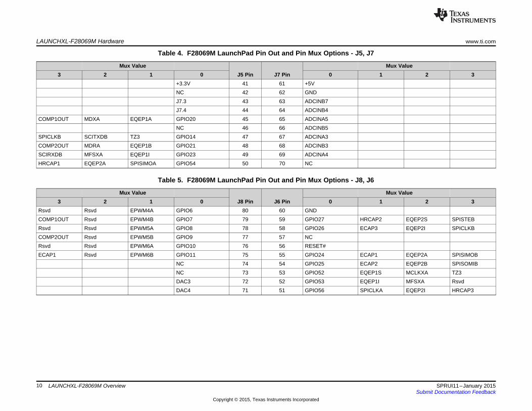
Table 4. F28069M LaunchPad Pin Out and Pin Mux Options - J5, J7
Mux Value Mux Value3 2 1 0 J5 Pin J7 Pin 0 1 2 3
+3.3V 41 61 +5VNC 42 62 GNDJ7.3 43 63 ADCINB7J7.4 44 64 ADCINB4
COMP1OUT MDXA EQEP1A GPIO20 45 65 ADCINA5NC 46 66 ADCINB5
SPICLKB SCITXDB TZ3 GPIO14 47 67 ADCINA3COMP2OUT MDRA EQEP1B GPIO21 48 68 ADCINB3SCIRXDB MFSXA EQEP1I GPIO23 49 69 ADCINA4HRCAP1 EQEP2A SPISIMOA GPIO54 50 70 NC
Table 5. F28069M LaunchPad Pin Out and Pin Mux Options - J8, J6
Mux Value Mux Value3 2 1 0 J8 Pin J6 Pin 0 1 2 3
Rsvd Rsvd EPWM4A GPIO6 80 60 GNDCOMP1OUT Rsvd EPWM4B GPIO7 79 59 GPIO27 HRCAP2 EQEP2S SPISTEBRsvd Rsvd EPWM5A GPIO8 78 58 GPIO26 ECAP3 EQEP2I SPICLKBCOMP2OUT Rsvd EPWM5B GPIO9 77 57 NCRsvd Rsvd EPWM6A GPIO10 76 56 RESET#ECAP1 Rsvd EPWM6B GPIO11 75 55 GPIO24 ECAP1 EQEP2A SPISIMOB
NC 74 54 GPIO25 ECAP2 EQEP2B SPISOMIBNC 73 53 GPIO52 EQEP1S MCLKXA TZ3DAC3 72 52 GPIO53 EQEP1I MFSXA RsvdDAC4 71 51 GPIO56 SPICLKA EQEP2I HRCAP3
10 LAUNCHXL-F28069M Overview SPRUI11–January 2015Submit Documentation Feedback
Copyright © 2015, Texas Instruments Incorporated

1.1
BL
OC
KD
IAG
RA
M
Sheet 2
Sheet 2
Sheet 3&
4
Sheet 2
Sheet 5
Sheet 5
Sheet 5
Sheet5
Sheet 4
RE
VD
ATA
NO
TE
RE
V1.0
RE
V1.1
20140806
20140922
OR
IGIN
AL
RE
LE
AS
ED
Add p
ullu
pre
sis
tances a
nd filt
er
capacitors
for
QE
Pnet on s
heet5.
Pow
er
managem
ent
Mic
ro U
SB
type B
FT
2232H
TM
S320F
28069
Booste
rPack 1
Connecto
r
LE
DS
CA
N
SE
RIA
L1&
2
Booste
rPack
2 C
onnecto
r
QE
PC
onnecto
r
Ro
yY
au
ng
A B C D E
A B C D E
12
34
56
No
te:
DN
P=
Do
No
t P
op
ula
te
www.ti.com LAUNCHXL-F28069M Hardware
6.2 SchematicsFigure 2 shows the F28069M LaunchPad schematic.
Figure 2. LAUNCHXL-F28069_B_1400922 Block Diagram Schematic
11SPRUI11–January 2015 LAUNCHXL-F28069M OverviewSubmit Documentation Feedback
Copyright © 2015, Texas Instruments Incorporated

1.1
US
BT
OJT
AG
Vo
ut
= 3
.3V
Iou
t =
1A
CD
RH
2D
18/H
PN
P-2
R2N
C
2.2
k3.3
u
0.1
u
93LC
56B
T-I
/OT
0.1
u0.1
u0.1
u
12k
1K
ISO
7231
ISO
7240
AG
ND
AG
ND
AG
ND
AG
ND
AG
ND
AG
ND
GN
D
GN
D
1K
AG
ND
330
330
12M
36p
36p
+3V
3
00000
0 0 00
+3V
3
AG
ND
AG
ND
AG
ND
AG
ND
4.7u
4.7u
BLM15AG601SN1D
BLM15AG601SN1D
AGND
AGND
500m
A
+5V
0R
0R
AG
ND
0.1
u
AG
ND
AG
ND
AG
ND
820
AG
ND
TP
S62162D
SG
R
100K
10uF
22uF
2.2
uH AGND
10K
R31C
15
C16
VC
C
GN
D
6 2
CL
K4
DO
1
DI
3
CS
5
U8
VR
EG
INP
$5
0
US
BD
MP
$7
US
BD
PP
$8
RE
FP
$6
RE
SE
T#
P$
14
OS
CI
P$
2
OS
CO
P$
3
EE
CS
P$
63
EE
CL
KP
$6
2
EE
DA
TA
P$
61
TE
ST
P$
13
AGND P$10
GND1 P$1
GND2 P$5
GND3 P$11
GND4 P$15
PW
RE
N#
P$
60
SU
SP
EN
D#
P$
36
BC
BU
S3
P$
54
BC
BU
S2
P$
53
BC
BU
S1
P$
52
BC
BU
S0
P$
48
BD
BU
S7
P$
46
BD
BU
S6
P$
45
BD
BU
S5
P$
44
BD
BU
S4
P$
43
BD
BU
S3
P$
41
BD
BU
S2
P$
40
BD
BU
S1
P$
39
BD
BU
S0
P$
38
AC
BU
S3
P$
29
AC
BU
S2
P$
28
AC
BU
S1
P$
27
AC
BU
S0
P$
26
AD
BU
S7
P$
24
AD
BU
S6
P$
23
AD
BU
S5
P$
22
AD
BU
S4
P$
21
AD
BU
S3
P$
19
AD
BU
S2
P$
18
AD
BU
S1
P$
17
AD
BU
S0
P$
16
VCCIO1P$20
VCORE2P$37VCORE1P$12
VPHYP$4
AC
BU
S4
P$
30
AC
BU
S5
P$
32
AC
BU
S6
P$
33
AC
BU
S7
P$
34
BC
BU
S4
P$
55
BC
BU
S5
P$
57
BC
BU
S6
P$
58
BC
BU
S7
P$
59
GND5 P$25
GND6 P$35
GND7 P$47
GND8 P$51
VR
EG
OU
TP
$4
9
VPLLP$9
VCORE3P$64
VCCIO2P$31
VCCIO3P$42
VCCIO4P$56
TH TH
U6
FT
2232H
C14
C13
C12
R24
R22
1 2 3 4 5
VC
C1
1V
CC
21
6
GN
D1
2
GN
D1
8
GN
D2
15
GN
D2
9
INA
3
INB
4
OU
TC
5
NC
16
EN
17
EN
21
0
OU
TA
14
OU
TB
13
INC
12
NC
211
U7
VC
C1
1V
CC
21
6
GN
D1
2
GN
D1
8
GN
D2
15
GN
D2
9
INA
3
INB
4
INC
5
IND
6
NC
7E
N1
0
OU
TA
14
OU
TB
13
OU
TC
12
OU
TD
11
U5
R23
D7
D8
R26
R27
Q3 C17
C18
R21
R20
R19
R18
R16
R28
R30
R32
R251
2
JP
1 JP2 12
C10
C11
L2
L1
F1
12
JP
3
R15
R33
TP
10
TP
11
TP
12 T
P13
TP
14T
P15T
P16T
P17
C43
D4
R46
TP
30
EN
P$
3
EX_PAD P$9
FB
P$
5
GN
DP
$4
PG
P$
8P
GN
DP
$1
SW
P$
7V
INP
$2
VO
SP
$6
U17
R47
C44
C45
L7
R12
D-
D-
D+
D+
US
BV
CC
US
BV
CC
TC
KT
DI
TD
OTM
S
FT
DI_
CS
FT
DI_
CS
FT
DI_
CLK
FT
DI_
CLK
FT
DI_
DA
TA
FT
DI_
DA
TA
FT
DI_
DA
TA
FT
DI_
1V
8
PW
RE
N#
SU
SP
EN
D#
SC
I_R
X
SC
I_T
X
FT
DI_
3V
3F
TD
I_3V
3
FT
DI_
3V
3
FT
DI_
3V
3
FT
DI_
3V
3
FT
DI_
3V
3
FT
DI_
3V
3F
TD
I_3V
3
JTA
G_T
RS
T
LP
_5V
Ro
yY
au
ng
ArrayEEPROM
A B C D E
A B C D E
12
34
56
Min
iU
SB
LAUNCHXL-F28069M Hardware www.ti.com
Figure 3. LAUNCHXL-F28069_B_1400922 USB to JTAG Schematic
12 LAUNCHXL-F28069M Overview SPRUI11–January 2015Submit Documentation Feedback
Copyright © 2015, Texas Instruments Incorporated
1.0
F2
80
69
_A
PW
M
TD
OG
PIO
34
TR
ST
10
00 0 0 0
xx
0 1 1
1 10
Em
ula
tio
nB
oo
tP
ara
llel I/
OS
CI
Wa
itG
etM
ode
RE
SE
TB
OO
T
+3
V3
36p36p
1M
GN
D
GN
D
2.2k
2.2k
2.2k
820
820
+3
V3
+3
V3
GN
DG
ND
2.2
u2
.2u
TP
-113
8K
9-B
E11
25
GN
D
820
+3
V3
GN
D
20
4-3
ST
2.2k GN
D
BKP1005HS221-T
BLM15PD600SN1D
2.2
u2
.2u
2.2
u
GN
D
TM
S3
20
F2
806
9M
PZ
T
TM
S32
0F
28
06
9M
PZ
T
2.2
u2
.2u
2.2
u2
.2u
GN
D 2.2
u2
.2u
2.2
u2
.2u
2.2
u
GN
D
+3
V3
+3
V3
GN
D
GN
D
0.1
u
0.1
u
GN
DQ1
C4C3
R7
R6
R8
R9
R4
R5C
5C
6
S2
D1
R1
S1
4561 2 3
R10
L3
L4
C1
9C
20
C2
1
TR
ST
12
VR
EG
EN
Z9
0
XR
S11
AD
C_
INA
02
3A
DC
_IN
A1
22
AD
C_
INA
2/C
OM
P1
A/A
IO2
21
AD
C_
INA
32
0A
DC
_IN
A4
/CO
MP
2A
/AIO
41
9A
DC
_IN
A5
18
AD
C_
INA
6/C
OM
P3
A/A
IO6
17
AD
C_
INA
71
6
AD
C_
INB
02
8A
DC
_IN
B1
29
AD
C_
INB
2/C
OM
P1
B/A
IO1
03
0A
DC
_IN
B3
31
AD
C_
INB
4/C
OM
P2
B/A
IO1
23
2A
DC
_IN
B5
33
AD
C_
INB
6/C
OM
P3
B/A
IO1
43
4A
DC
_IN
B7
35
TC
K/G
PIO
38
67
TD
I/G
PIO
35
71
TD
O/G
PIO
37
70
TE
ST
24
5
TM
S/G
PIO
36
72
VD
D_
FL
46
VR
EF
HI
24
VR
EF
LO
27
X1
60
X2
59
XC
LK
_I/
GP
IO1
96
4
XC
LK
_O
/GP
IO1
85
1
U1
G$
1
VD
D1
3
VD
D2
14
VD
D3
37
VD
D4
63
VD
D5
81
VD
D6
91
VD
DA
25
VD
DIO
15
VD
DIO
21
3
VD
DIO
33
8
VD
DIO
46
1
VD
DIO
57
9
VD
DIO
69
3
VS
S1
4
VS
S2
15
VS
S3
36
VS
S4
47
VS
S5
62
VS
S6
80
VS
S7
92
VS
SA
26
U1
G$
3
C1
C2
C2
2C
23
C2
6C
27
C2
8C
29
C3
0
TP
18
TP
19
TP
20
TP
21
TP
22
TP
23
TP
24
C3
9
C4
0
TC
K
TD
IT
DO
TD
O
TM
S
TR
ST
TR
ST
RE
SE
T#
RE
SE
T#
GP
IO3
4
AD
CIN
A6
AD
CIN
A4
AD
CIN
A1
AD
CIN
A2
AD
CIN
B1
AD
CIN
B2
AD
CIN
B4
GP
IO1
8
JTA
G_T
RS
T
AD
CIN
A7
AD
CIN
A3
AD
CIN
A0
AD
CIN
B3
AD
CIN
B7
AD
CIN
B6
AD
CIN
A5
AD
CIN
B5
AD
CIN
B0
GP
IO1
9
Ro
yY
au
ng
1 2 3
ON
A B C D E
A B C D E
12
34
56
JTAG CLOCK
ADC
DN
P
www.ti.com LAUNCHXL-F28069M Hardware
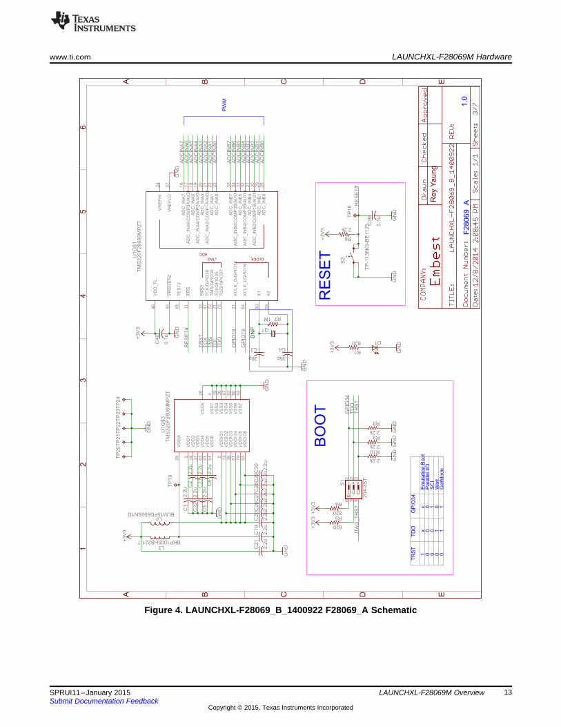
Figure 4. LAUNCHXL-F28069_B_1400922 F28069_A Schematic
13SPRUI11–January 2015 LAUNCHXL-F28069M OverviewSubmit Documentation Feedback
Copyright © 2015, Texas Instruments Incorporated
1.1
F2
80
69
_B
PW
MU
AR
T
PW
M_
DA
C
SN
74
LVC
2G
07
330
330
+3
V3
+3
V3
+3
V3
GN
D
TM
S3
20
F2
80
69
MP
ZT
1K
1K
1K
1K
0.1
u0
.1u
0.1
u0
.1u
GN
DG
ND
GN
DG
ND
0.1
u
GN
D
D9
D10
U9
1A
1
2A
32
Y4
1Y
6
VCC5 GND 2
R38
R39
GP
IO0
/EP
WM
1A
87
GP
IO1
/EP
WM
1B
/CO
MP
1O
UT
86
GP
IO2
/EP
WM
2A
84
GP
IO3
/EP
WM
2B
/SP
ISO
MIA
/CO
MP
2O
UT
83
GP
IO4
/EP
WM
3A
9
GP
IO5
/EP
WM
3B
/SP
ISIM
OA
/EC
AP
11
0
GP
IO6
/EP
WM
4A
/EP
WM
SY
NC
I/E
PW
MS
YN
CO
58
GP
IO7
/EP
WM
4B
/SC
IRX
DA
/EC
AP
25
7
GP
IO8
/EP
WM
5A
/AD
CS
OC
AO
54
GP
IO9
/EP
WM
5B
/SC
I_T
XD
B/E
CA
P4
9
GP
IO1
0/E
PW
M6
A/A
DC
SO
CB
O7
4
GP
IO11
/EP
WM
6B
/SC
I_R
XD
B/E
CA
P1
73
GP
IO1
2/T
Z1
/SC
ITX
DA
/SP
ISIM
OB
44
GP
IO1
3/T
Z2
/SP
ISO
MIB
95
GP
IO1
4/T
Z3
/SC
ITX
DB
/SP
ICL
KB
96
GP
IO1
5/E
CA
P2
/SC
I_R
XD
B/S
PIS
TE
B8
8
GP
IO1
6/S
PI_
SIM
O_
A/T
Z2
55
GP
IO1
7/S
PI_
SO
MI_
A/T
Z3
52
GP
IO2
0/E
QE
P1
A/M
DX
A/C
OM
P1
OU
T6
GP
IO2
1/E
QE
P1
B/M
DR
A/C
OM
P2
OU
T7
GP
IO2
2/E
QE
P1
S/M
CL
KX
A/S
CIT
XD
B9
8G
PIO
23
/EQ
EP
1I/
MF
SX
A/S
CIR
XD
B2
GP
IO2
4/E
CA
P1
/EQ
EP
2A
/SP
ISIM
OB
97
GP
IO2
5/E
CA
P2
/EQ
EP
2B
/SP
ISO
MIB
39
GP
IO2
6/E
CA
P3
/EQ
EP
2I/
SP
ICL
KB
/US
B0
DP7
8
GP
IO2
7/H
RC
AP
2/E
QE
P2
S/S
PIS
TE
B/U
SB
0D
M77
GP
IO2
8/S
CI_
RX
DA
/SD
AA
/TZ
25
0
GP
IO2
9/S
CI_
TX
DA
/SC
LA
/TZ
34
3
GP
IO3
0/C
AN
_R
XA
/EQ
EP
2I/
EP
WM
7A
41
GP
IO3
1/C
AN
_T
XA
/EQ
EP
2S
/EP
WM
8A
40
GP
IO3
2/S
DA
_A
/EP
WM
SY
NC
I/A
DC
SO
CA
O9
9
GP
IO3
3/S
CL
_A
/EP
WM
SY
NC
O/A
DC
SO
CB
O1
00
GP
IO3
4/C
OM
P2
OU
T/C
OM
P3
OU
T6
8
GP
IO3
96
6
GP
IO4
0/E
PW
M7
A/S
CI_
TX
DB
82
GP
IO4
1/E
PW
M7
B/S
CI_
RX
DB
76
GP
IO4
2/E
PW
M8
A/T
Z1
/CO
MP
1O
UT
1
GP
IO4
3/E
PW
M8
B/T
Z2
/CO
MP
2O
UT
8
GP
IO4
4/M
FS
RA
/SC
IRX
DB
/EP
WM
7B
56
GP
IO5
0/E
QE
P1
A/M
DX
A/T
Z1
42
GP
IO5
1/E
QE
P1
B/M
DR
A/T
Z2
48
GP
IO5
2/E
QE
P1
S/M
CL
KX
A/T
Z3
53
GP
IO5
3/E
QE
P1
I/M
FS
XA
65
GP
IO5
4/S
PIS
IMO
A/E
QE
P2
A/H
RC
AP
16
9
GP
IO5
5/S
PIS
OM
IA/E
QE
P2
B/H
RC
AP
27
5
GP
IO5
6/S
PIC
LK
A/E
QE
P2
I/H
RC
AP
38
5
GP
IO5
7/S
PIS
TE
A/E
QE
P2
S/H
RC
AP
48
9
GP
IO5
8/M
CL
KR
A/S
CI_
TX
DB
/EP
WM
7A
94
U1
G$
2
R3
6
R3
7
R4
0
R4
1
C3
3C
34
C3
5C
36
C2
4
TP
5
TP
6
TP
7
TP
8
GP
IO1
7G
PIO
16
GP
IO1
GP
IO0
GP
IO3
2
GP
IO2
GP
IO3
GP
IO4
GP
IO5
GP
IO6
GP
IO7
GP
IO1
2
GP
IO2
8
GP
IO3
3
GP
IO8
GP
IO2
9
GP
IO4
4G
PIO
50
GP
IO5
1
GP
IO2
2
GP
IO1
3G
PIO
14
GP
IO9
GP
IO1
0G
PIO
11G
PIO
40
GP
IO4
0
GP
IO4
1
GP
IO4
1
GP
IO4
2
GP
IO4
2
GP
IO4
3
GP
IO4
3
GP
IO2
6G
PIO
27
GP
IO2
5
GP
IO5
2G
PIO
53
GP
IO2
4
GP
IO2
0G
PIO
21
GP
IO2
3
GP
IO5
4G
PIO
55
GP
IO5
6
GP
IO3
0G
PIO
31
GP
IO5
8G
PIO
15
GP
IO3
4
GP
IO3
4
GP
IO3
9
GP
IO3
9
DA
C1
DA
C2
DA
C3
DA
C4
GP
IO5
7G
PIO
57
Ro
yY
au
ng
A B C D E
A B C D E
12
34
56
LAUNCHXL-F28069M Hardware www.ti.com
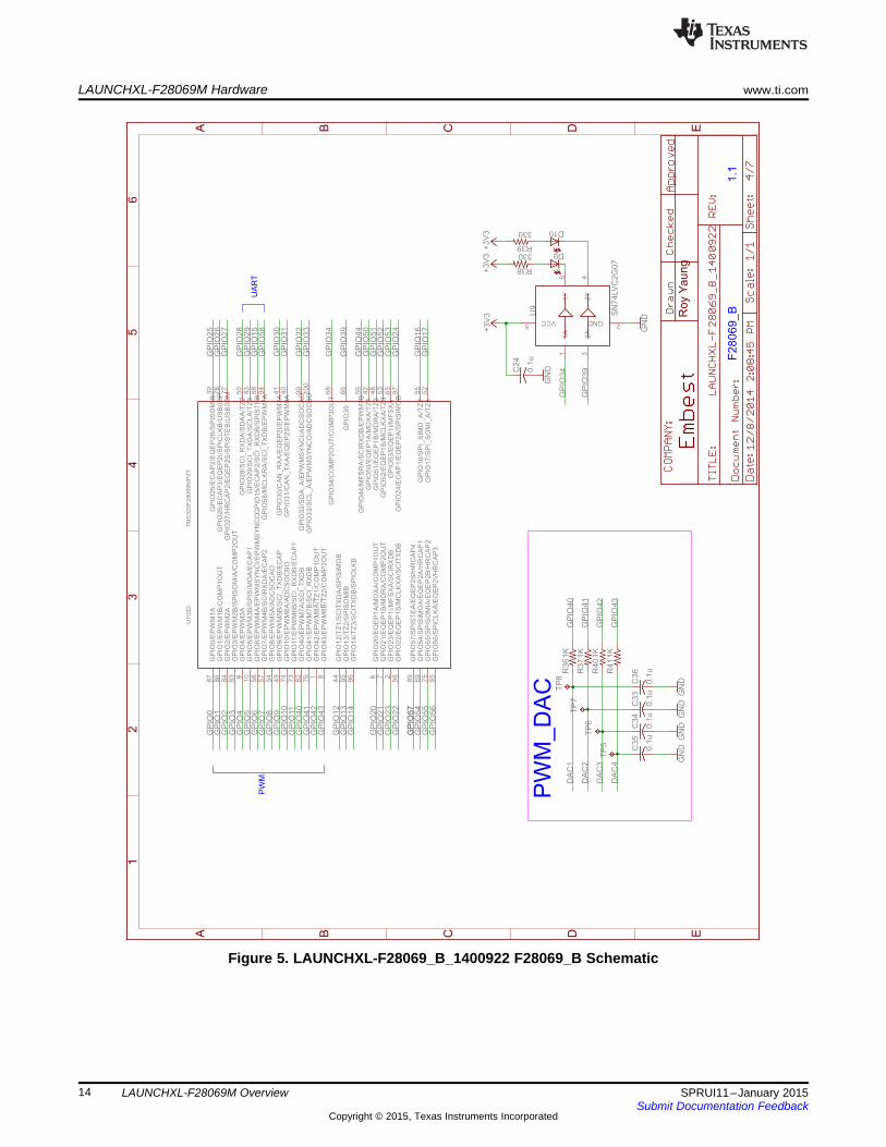
Figure 5. LAUNCHXL-F28069_B_1400922 F28069_B Schematic
14 LAUNCHXL-F28069M Overview SPRUI11–January 2015Submit Documentation Feedback
Copyright © 2015, Texas Instruments Incorporated

1.1
CO
NN
EC
TO
R
Vdc
V_A
1V
_B
1V
_C
1I_
A1
I_B
1I_
C1
V_A
2V
_B
2V
_C
2I_
A2
I_B
2I_
C2
PW
R
PW
R
PW
RA
NA
FA
ULT
nO
CT
Wn
GP
IOA
NA
GP
IO1S
PI_
CLK
1P
WM
_A
H1P
WM
_A
L1P
WM
_B
H1P
WM
_B
L1P
WM
_C
H1P
WM
_C
LG
PIO
GN
D1S
PI_
CS
GP
IO
RE
SE
T1S
PI_
SI
1S
PI_
SO
1E
N_G
AT
E1D
C_C
AL
PW
RA
NA
FA
ULT
nO
CT
Wn
AN
A2S
PI_
CLK
SC
LS
DA
2P
WM
_A
H2P
WM
_A
L2P
WM
_B
H2P
WM
_B
L2P
WM
_C
H2P
WM
_C
L
PW
M_D
AC
GN
D2S
PI_
CS
GP
IO
RE
SE
T2S
PI_
SI
2S
PI_
SO
2E
N_G
AT
E2D
C_C
AL
A B I GN
DP
WR
GN
D
GN
D
PW
M_D
AC
PW
M_D
AC
PW
M_D
AC
CA
N
LE
VE
LS
HIF
T
Vdc
+3V
3
GN
D
GN
D
+5VGN
D
GN
D+3V3
+5V
TX
B0106P
WR
+5V
+5V
GN
DG
ND
+5V
+3V
3
2.2
k
GND
120
10K 10K
0R 0R
+3V
3
GN
DG
ND
0.1u
GN
D
0.1u
GN
D
0.1u
GN
D
GN
D
+3V
3
PG
ND
1K
1K
1K
0.001u
0.001u
0.001u
1K
1K
1K
0.001u
0.001u
0.001uJ1
J4
J2
12
JP
4
12
JP
5
J3
J7
J5 J8
J6
A1
P$
1
A2
P$
3
A3
P$
4
A4
P$
5
A5
P$
6
A6
P$
7
B1
P$
16
B2
P$
14
B3
P$
13
B4
P$
12
B5
P$
11
B6
P$
10
GN
DP
$9
OE
P$
8
VC
CA
P$
2V
CC
BP
$1
5
U2
1 2 3 4 5
QE
P_A
1 2 3 4 5
QE
P_B
R2
CA
NH
P$
7
CA
NL
P$
6D
P$
1
EN
P$
5
GND P$2
RP
$4
RS
P$
8
VCCP$3
U3
SN
65H
VD
234D
R34
1 2 3
J12
R35
R42
R43
R44
C31
C32
C37
1 2 3
J9
R13
R29
R48
C50
C51
C52
R49
R50
R51
C53
C54
C55
RE
SE
T#
RE
SE
T#
GP
IO19
GP
IO17
GP
IO16
GP
IO1
GP
IO0
GP
IO32
GP
IO2
GP
IO3
GP
IO4
GP
IO5
GP
IO6
GP
IO7
GP
IO12
AD
CIN
A6
AD
CIN
A4
AD
CIN
A2
AD
CIN
B2
AD
CIN
B4
GP
IO18
GP
IO33
AD
CIN
A1
AD
CIN
B1
AD
CIN
A3
AD
CIN
A0
AD
CIN
B3
AD
CIN
B7
AD
CIN
A5
AD
CIN
B0
GP
IO22
GP
IO13
AD
CIN
B5
GP
IO14
GP
IO24
GP
IO27
GP
IO26
GP
IO25
GP
IO52
GP
IO53
GP
IO8
GP
IO9
GP
IO10
GP
IO11
GP
IO50
GP
IO51
GP
IO44
GP
IO20
GP
IO20
GP
IO21
GP
IO21
GP
IO23
GP
IO23
GP
IO54
GP
IO54
GP
IO55
GP
IO55
GP
IO56
GP
IO56
EQ
EP
1A
EQ
EP
1A
EQ
EP
1B
EQ
EP
1B
EQ
EP
1I
EQ
EP
1I
EQ
EP
2A
EQ
EP
2A
EQ
EP
2B
EQ
EP
2B
EQ
EP
2I
EQ
EP
2I
AD
CIN
B6
DA
C1
DA
C2
DA
C3
DA
C4
GP
IO30
GP
IO31
CA
NH
CA
NL
AD
CIN
A7
J7.3
J7.4
J1.3
J1.4
Roy
Yau
ng
A B C D E
A B C D E
12
34
56
1 2 3 4 5 6 7 8 9 10
41
42
43
44
45
46
47
48
49
50
1112
13
14
15
16
17
18
19
20
51
52
53
54
55
56
57
58
59
60
21
22
23
24
25
26
27
28
29
30
61
62
63
64
65
66
67
68
69
70
31
32
33
34
35
36
37
38
39
40
71
72
73
74
75
76
77
78
79
80
www.ti.com LAUNCHXL-F28069M Hardware
Figure 6. LAUNCHXL-F28069_B_1400922 Connector Schematic
15SPRUI11–January 2015 LAUNCHXL-F28069M OverviewSubmit Documentation Feedback
Copyright © 2015, Texas Instruments Incorporated

1.1
Lo
gic
Ch
oic
e
MU
X_S
ELC
H_S
EL
00 0
1
UA
RT
Dis
able
; G
PIO
28&
29
—J1.3
& J
1.4
; G
PIO
15&
58
—J7.3
& J
7.4
.
U11
& U
15
Dis
able
; G
PIO
15&
58
—J7.3
& J
7.4
;G
PIO
28&
29
—U
AR
T.
Channel D
escription
1 1
0 1
U16 D
isable
; G
PIO
28&
29
—F
ault
& O
ctw
;G
PIO
15&
58
—U
AR
T.
U16 D
isable
; G
PIO
28&
29
—F
ault
& O
ctw
;G
PIO
15&
58
—U
AR
T.
MU
X2
MU
X1
OR
G
GN
D
SN
74A
HC
1G
32
+3V
3
0.1u
GN
D
SN
74A
HC
1G
32
+3V
3
0.1u
GN
D
SN
74LV
4052A
PW
0.1u
GND
+3V
3
GN
D
GN
D
TS
5A
31
53
DC
UR
+3V
3
0.1u
GND
GN
D
TS
5A
31
53
DC
UR
+3V
3
0.1u
GNDG
ND
GN
D
TS
5A
23
15
9D
GS
R
+3V
3
GN
D
+3V
3
0.1u
GND
GN
D
10K
10K
+3V
3
0.1u
GN
D
GN
D
SN
74LV
C1G
04D
CK
R
0.1
u GN
D
+3V
3
SN
74A
HC
1G
02D
BV
R
A1
B2
GND 3VCC5
Y4
U13
C46
A1
B2
GND 3VCC5
Y4
U14
C47
1C
OM
P$
13
1Y
0P
$1
2
1Y
1P
$1
4
1Y
2P
$1
5
1Y
3P
$11
2C
OM
P$
32
Y0
P$
1
2Y
1P
$5
2Y
2P
$2
2Y
3P
$4
GND1 P$8
GND2 P$7
INH
P$
6S
0P
$1
0
S1
P$
9
VCCP$16
U10
C38
12
JP6T
P25
TP
26
EN
P$
2
CO
MP
$1
GN
D1
P$
3
GN
D2
P$
4IN
P$
5
NC
P$
7
NO
P$
6V
+P
$8
U11
C48
EN
P$
2
CO
MP
$1
GN
D1
P$
3
GN
D2
P$
4IN
P$
5
NC
P$
7
NO
P$
6V
+P
$8
U1
5
C49
CO
M1
P$
10
CO
M2
P$
6
IN1
P$
1
IN2
P$
5
NC
1P
$9
NC
2P
$7
NO
1P
$2
NO
2P
$4
V+P$8 V- P$3
U1
6
12
JP7
C42
TP
3
TP
4
TP
9
TP
27
TP
28
TP
29
R3
R11
C7
TP
12
4
U18A
35 U18P
GNDVCC
C9
A1
B2
GND 3VCC5
Y4
U4
GP
IO28
GP
IO28
GP
IO29
GP
IO29
FA
ULT
_O
FA
ULT
_O
OC
TW
_O
OC
TW
_O
J1.3
J1.3
J7.3
J7.3
J7.4
J7.4
J1.4
J1.4
GP
IO58
GP
IO58
GP
IO15
GP
IO15
SC
I_R
X
SC
I_T
X
CH
_S
EL
CH
_S
EL
CH
_S
EL
MU
X_S
EL
MUX_SELMU
X_S
EL
MU
X_S
EL
MU
X_S
EL
EN
EN
Ro
yY
au
ng
A B C D E
A B C D E
12
34
56
LAUNCHXL-F28069M Hardware www.ti.com
Figure 7. LAUNCHXL-F28069_B_1400922 Logic Choice Schematic
16 LAUNCHXL-F28069M Overview SPRUI11–January 2015Submit Documentation Feedback
Copyright © 2015, Texas Instruments Incorporated

1.1
Po
we
r
Vo
ut
= 5
VIo
ut
=0
.5A
CD
RH
3D
16/H
PN
P-3
R3N
C
82
0p
LM
R6
24
21
XM
FE
/NO
PB
10K
3.3
uH
1N
58
19
HW
-7-F
10
uF
30.1K 10K
4.7
u
+3
V3
GN
DG
ND
C2
5
FB
3
GND2
SD
4
SW
ITC
H1
VIN
5
U1
2
R14
L6
D3
C4
1
R17 R45
TP
2
C8
LP
_5
V
Ro
yY
au
ng
A B C D E
A B C D E
12
34
56
www.ti.com LAUNCHXL-F28069M Hardware
Figure 8. LAUNCHXL-F28069_B_1400922 Power Schematic
17SPRUI11–January 2015 LAUNCHXL-F28069M OverviewSubmit Documentation Feedback
Copyright © 2015, Texas Instruments Incorporated
LAUNCHXL-F28069M Hardware www.ti.com
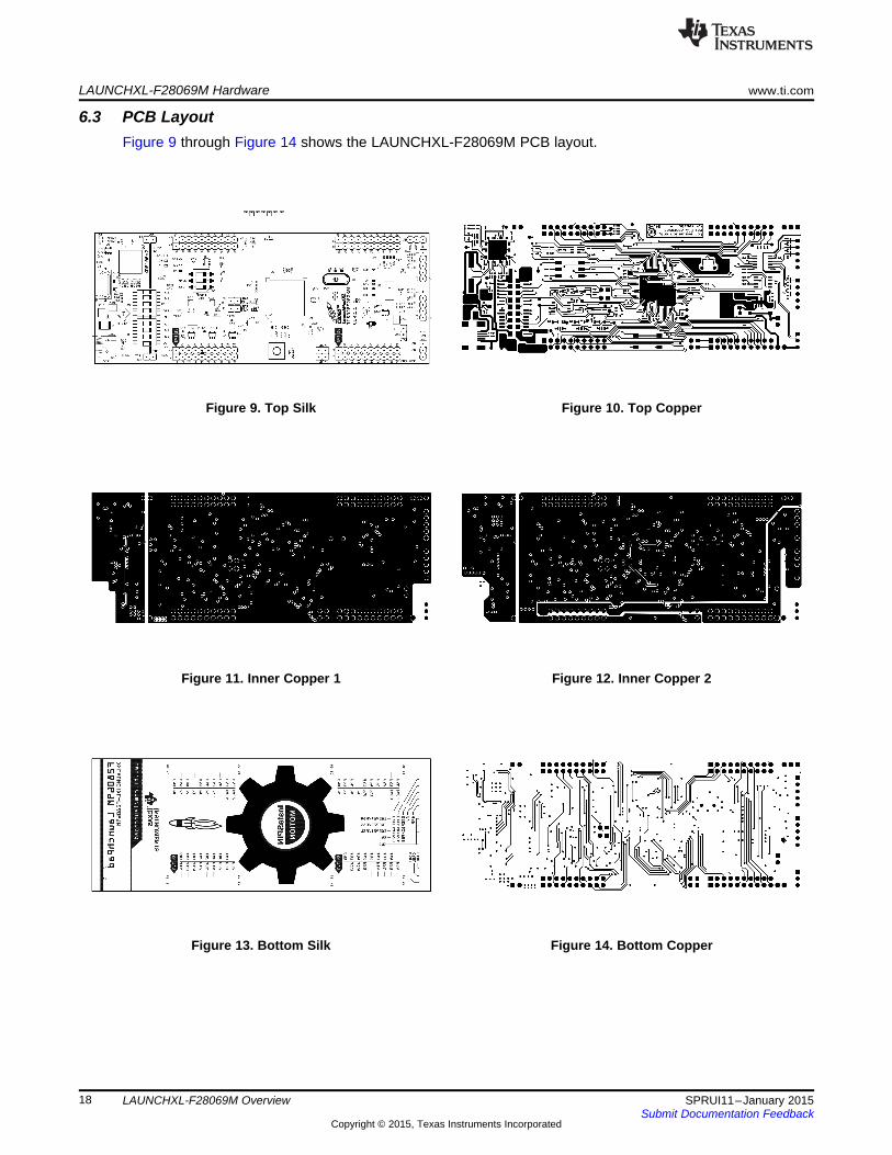
6.3 PCB LayoutFigure 9 through Figure 14 shows the LAUNCHXL-F28069M PCB layout.
Figure 9. Top Silk Figure 10. Top Copper
Figure 11. Inner Copper 1 Figure 12. Inner Copper 2
Figure 13. Bottom Silk Figure 14. Bottom Copper
18 LAUNCHXL-F28069M Overview SPRUI11–January 2015Submit Documentation Feedback
Copyright © 2015, Texas Instruments Incorporated
www.ti.com LAUNCHXL-F28069M Hardware
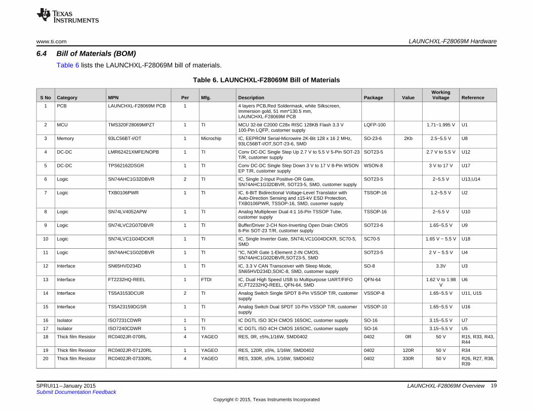
6.4 Bill of Materials (BOM)Table 6 lists the LAUNCHXL-F28069M bill of materials.
Table 6. LAUNCHXL-F28069M Bill of MaterialsWorking
S No Category MPN Per Mfg. Description Package Value Voltage Reference
1 PCB LAUNCHXL-F28069M PCB 1 4 layers PCB,Red Soldermask, white Silkscreen,Immersion gold, 51 mm*130.5 mm,LAUNCHXL-F28069M PCB
2 MCU TMS320F28069MPZT 1 TI MCU 32-bit C2000 C28x RISC 128KB Flash 3.3 V LQFP-100 1.71~1.995 V U1100-Pin LQFP, customer supply
3 Memory 93LC56BT-I/OT 1 Microchip IC, EEPROM Serial-Microwire 2K-Bit 128 x 16 2 MHz, SO-23-6 2Kb 2.5~5.5 V U893LC56BT-I/OT,SOT-23-6, SMD
4 DC-DC LMR62421XMFE/NOPB 1 TI Conv DC-DC Single Step Up 2.7 V to 5.5 V 5-Pin SOT-23 SOT23-5 2.7 V to 5.5 V U12T/R, customer supply
5 DC-DC TPS62162DSGR 1 TI Conv DC-DC Single Step Down 3 V to 17 V 8-Pin WSON WSON-8 3 V to 17 V U17EP T/R, customer supply
6 Logic SN74AHC1G32DBVR 2 TI IC, Single 2-Input Positive-OR Gate, SOT23-5 2~5.5 V U13,U14SN74AHC1G32DBVR, SOT23-5, SMD, customer supply
7 Logic TXB0106PWR 1 TI IC, 6-BIT Bidirectional Voltage-Level Translator with TSSOP-16 1.2~5.5 V U2Auto-Direction Sensing and ±15-kV ESD Protection,TXB0106PWR, TSSOP-16, SMD, cusomer supply
8 Logic SN74LV4052APW 1 TI Analog Multiplexer Dual 4:1 16-Pin TSSOP Tube, TSSOP-16 2~5.5 V U10customer supply
9 Logic SN74LVC2G07DBVR 1 TI Buffer/Driver 2-CH Non-Inverting Open Drain CMOS SOT23-6 1.65~5.5 V U96-Pin SOT-23 T/R, customer supply
10 Logic SN74LVC1G04DCKR 1 TI IC, Single Inverter Gate, SN74LVC1G04DCKR, SC70-5, SC70-5 1.65 V ~ 5.5 V U18SMD
11 Logic SN74AHC1G02DBVR 1 TI "IC, NOR Gate 1-Element 2-IN CMOS, SOT23-5 2 V ~ 5.5 V U4SN74AHC1G02DBVR,SOT23-5, SMD
12 Interface SN65HVD234D 1 TI IC, 3.3 V CAN Transceiver with Sleep Mode, SO-8 3.3V U3SN65HVD234D,SOIC-8, SMD, customer supply
13 Interface FT2232HQ-REEL 1 FTDI IC, Dual High Speed USB to Multipurpose UART/FIFO QFN-64 1.62 V to 1.98 U6IC,FT2232HQ-REEL, QFN-64, SMD V
14 Interface TS5A3153DCUR 2 TI Analog Switch Single SPDT 8-Pin VSSOP T/R, customer VSSOP-8 1.65~5.5 V U11, U15supply
15 Interface TS5A23159DGSR 1 TI Analog Switch Dual SPDT 10-Pin VSSOP T/R, customer VSSOP-10 1.65~5.5 V U16supply
16 Isolator ISO7231CDWR 1 TI IC DGTL ISO 3CH CMOS 16SOIC, customer supply SO-16 3.15~5.5 V U7
17 Isolator ISO7240CDWR 1 TI IC DGTL ISO 4CH CMOS 16SOIC, customer supply SO-16 3.15~5.5 V U5
18 Thick film Resistor RC0402JR-070RL 4 YAGEO RES, 0R, ±5%,1/16W, SMD0402 0402 0R 50 V R15, R33, R43,R44
19 Thick film Resistor RC0402JR-07120RL 1 YAGEO RES, 120R, ±5%, 1/16W, SMD0402 0402 120R 50 V R34
20 Thick film Resistor RC0402JR-07330RL 4 YAGEO RES, 330R, ±5%, 1/16W, SMD0402 0402 330R 50 V R26, R27, R38,R39
19SPRUI11–January 2015 LAUNCHXL-F28069M OverviewSubmit Documentation Feedback
Copyright © 2015, Texas Instruments Incorporated
LAUNCHXL-F28069M Hardware www.ti.com
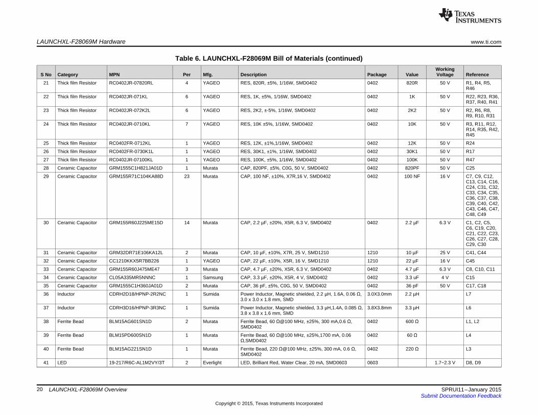
Table 6. LAUNCHXL-F28069M Bill of Materials (continued)Working
S No Category MPN Per Mfg. Description Package Value Voltage Reference
21 Thick film Resistor RC0402JR-07820RL 4 YAGEO RES, 820R, ±5%, 1/16W, SMD0402 0402 820R 50 V R1, R4, R5,R46
22 Thick film Resistor RC0402JR-071KL 6 YAGEO RES, 1K, ±5%, 1/16W, SMD0402 0402 1K 50 V R22, R23, R36,R37, R40, R41
23 Thick film Resistor RC0402JR-072K2L 6 YAGEO RES, 2K2, ±-5%, 1/16W, SMD0402 0402 2K2 50 V R2, R6, R8,R9, R10, R31
24 Thick film Resistor RC0402JR-0710KL 7 YAGEO RES, 10K ±5%, 1/16W, SMD0402 0402 10K 50 V R3, R11, R12,R14, R35, R42,R45
25 Thick film Resistor RC0402FR-0712KL 1 YAGEO RES, 12K, ±1%,1/16W, SMD0402 0402 12K 50 V R24
26 Thick film Resistor RC0402FR-0730K1L 1 YAGEO RES, 30K1, ±1%, 1/16W, SMD0402 0402 30K1 50 V R17
27 Thick film Resistor RC0402JR-07100KL 1 YAGEO RES, 100K, ±5%, 1/16W, SMD0402 0402 100K 50 V R47
28 Ceramic Capacitor GRM1555C1H821JA01D 1 Murata CAP, 820PF, ±5%, C0G, 50 V, SMD0402 0402 820PF 50 V C25
29 Ceramic Capacitor GRM155R71C104KA88D 23 Murata CAP, 100 NF, ±10%, X7R,16 V, SMD0402 0402 100 NF 16 V C7, C9, C12,C13, C14, C16,C24, C31, C32,C33, C34, C35,C36, C37, C38,C39, C40, C42,C43, C46, C47,C48, C49
30 Ceramic Capacitor GRM155R60J225ME15D 14 Murata CAP, 2.2 µF, ±20%, X5R, 6.3 V, SMD0402 0402 2.2 µF 6.3 V C1, C2, C5,C6, C19, C20,C21, C22, C23,C26, C27, C28,C29, C30
31 Ceramic Capacitor GRM32DR71E106KA12L 2 Murata CAP, 10 µF, ±10%, X7R, 25 V, SMD1210 1210 10 µF 25 V C41, C44
32 Ceramic Capacitor CC1210KKX5R7BB226 1 YAGEO CAP, 22 µF, ±10%, X5R, 16 V, SMD1210 1210 22 µF 16 V C45
33 Ceramic Capacitor GRM155R60J475ME47 3 Murata CAP, 4.7 µF, ±20%, X5R, 6.3 V, SMD0402 0402 4.7 µF 6.3 V C8, C10, C11
34 Ceramic Capacitor CL05A335MR5NNNC 1 Samsung CAP, 3.3 µF, ±20%, X5R, 4 V, SMD0402 0402 3.3 uF 4 V C15
35 Ceramic Capacitor GRM1555C1H360JA01D 2 Murata CAP, 36 pF, ±5%, C0G, 50 V, SMD0402 0402 36 pF 50 V C17, C18
36 Inductor CDRH2D18/HPNP-2R2NC 1 Sumida Power Inductor, Magnetic shielded, 2.2 µH, 1.6A, 0.06 Ω, 3.0X3.0mm 2.2 µH L73.0 x 3.0 x 1.8 mm, SMD
37 Inductor CDRH3D16/HPNP-3R3NC 1 Sumida Power Inductor, Magnetic shielded, 3.3 µH,1.4A, 0.085 Ω, 3.8X3.8mm 3.3 µH L63.8 x 3.8 x 1.6 mm, SMD
38 Ferrite Bead BLM15AG601SN1D 2 Murata Ferrite Bead, 60 Ω@100 MHz, ±25%, 300 mA,0.6 Ω, 0402 600 Ω L1, L2SMD0402
39 Ferrite Bead BLM15PD600SN1D 1 Murata Ferrite Bead, 60 Ω@100 MHz, ±25%,1700 mA, 0.06 0402 60 Ω L4Ω,SMD0402
40 Ferrite Bead BLM15AG221SN1D 1 Murata Ferrite Bead, 220 Ω@100 MHz, ±25%, 300 mA, 0.6 Ω, 0402 220 Ω L3SMD0402
41 LED 19-217/R6C-AL1M2VY/3T 2 Everlight LED, Brilliant Red, Water Clear, 20 mA, SMD0603 0603 1.7~2.3 V D8, D9
20 LAUNCHXL-F28069M Overview SPRUI11–January 2015Submit Documentation Feedback
Copyright © 2015, Texas Instruments Incorporated
www.ti.com LAUNCHXL-F28069M Hardware
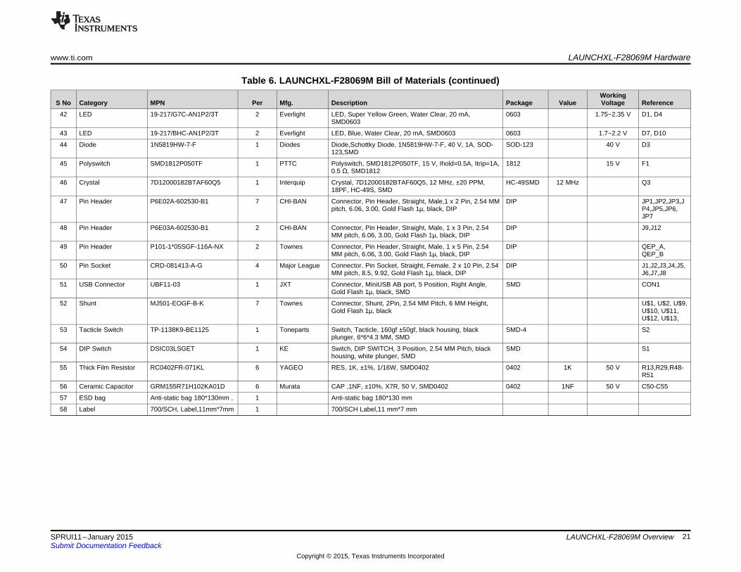
Table 6. LAUNCHXL-F28069M Bill of Materials (continued)Working
S No Category MPN Per Mfg. Description Package Value Voltage Reference
42 LED 19-217/G7C-AN1P2/3T 2 Everlight LED, Super Yellow Green, Water Clear, 20 mA, 0603 1.75~2.35 V D1, D4SMD0603
43 LED 19-217/BHC-AN1P2/3T 2 Everlight LED, Blue, Water Clear, 20 mA, SMD0603 0603 1.7~2.2 V D7, D10
44 Diode 1N5819HW-7-F 1 Diodes Diode,Schottky Diode, 1N5819HW-7-F, 40 V, 1A, SOD- SOD-123 40 V D3123,SMD
45 Polyswitch SMD1812P050TF 1 PTTC Polyswitch, SMD1812P050TF, 15 V, Ihold=0.5A, Itrip=1A, 1812 15 V F10.5 Ω, SMD1812
46 Crystal 7D12000182BTAF60Q5 1 Interquip Crystal, 7D12000182BTAF60Q5, 12 MHz, ±20 PPM, HC-49SMD 12 MHz Q318PF, HC-49S, SMD
47 Pin Header P6E02A-602530-B1 7 CHI-BAN Connector, Pin Header, Straight, Male,1 x 2 Pin, 2.54 MM DIP JP1,JP2,JP3,Jpitch, 6.06, 3.00, Gold Flash 1µ, black, DIP P4,JP5,JP6,
JP7
48 Pin Header P6E03A-602530-B1 2 CHI-BAN Connector, Pin Header, Straight, Male, 1 x 3 Pin, 2.54 DIP J9,J12MM pitch, 6.06, 3.00, Gold Flash 1µ, black, DIP
49 Pin Header P101-1*05SGF-116A-NX 2 Townes Connector, Pin Header, Straight, Male, 1 x 5 Pin, 2.54 DIP QEP_A,MM pitch, 6.06, 3.00, Gold Flash 1µ, black, DIP QEP_B
50 Pin Socket CRD-081413-A-G 4 Major League Connector, Pin Socket, Straight, Female, 2 x 10 Pin, 2.54 DIP J1,J2,J3,J4,J5,MM pitch, 8.5, 9.92, Gold Flash 1µ, black, DIP J6,J7,J8
51 USB Connector UBF11-03 1 JXT Connector, MiniUSB AB port, 5 Position, Right Angle, SMD CON1Gold Flash 1µ, black, SMD
52 Shunt MJ501-EOGF-B-K 7 Townes Connector, Shunt, 2Pin, 2.54 MM Pitch, 6 MM Height, U$1, U$2, U$9,Gold Flash 1µ, black U$10, U$11,
U$12, U$13,
53 Tacticle Switch TP-1138K9-BE1125 1 Toneparts Switch, Tacticle, 160gf ±50gf, black housing, black SMD-4 S2plunger, 6*6*4.3 MM, SMD
54 DIP Switch DSIC03LSGET 1 KE Switch, DIP SWITCH, 3 Position, 2.54 MM Pitch, black SMD S1housing, white plunger, SMD
55 Thick Film Resistor RC0402FR-071KL 6 YAGEO RES, 1K, ±1%, 1/16W, SMD0402 0402 1K 50 V R13,R29,R48-R51
56 Ceramic Capacitor GRM155R71H102KA01D 6 Murata CAP ,1NF, ±10%, X7R, 50 V, SMD0402 0402 1NF 50 V C50-C55
57 ESD bag Anti-static bag 180*130mm , 1 Anti-static bag 180*130 mm
58 Label 700/SCH, Label,11mm*7mm 1 700/SCH Label,11 mm*7 mm
21SPRUI11–January 2015 LAUNCHXL-F28069M OverviewSubmit Documentation Feedback
Copyright © 2015, Texas Instruments Incorporated

References www.ti.com
7 ReferencesThe following documents describe the C2000 devices. Copies of these documents are available on theInternet at http://www.ti.com/c2000 and www.ti.com/c2000-launchpad, or click on the links below:• TMS320F2806x Piccolo™ Microcontrollers Data Manual (SPRS698)• TMS320F28069, TMS320F28068, TMS320F28067, TMS320F28066, TMS320F28065,
TMS320F28064, TMS320F28063, TMS320F28062 Piccolo MCU Silicon Errata (SPRZ342)• TMS320x2806x Piccolo Technical Reference Guide (SPRUH18)• TMS320C28x Extended Instruction Sets Technical Reference Manual (SPRUHS1)• TMS320C28x Instruction Set Simulator Technical Overview (SPRU608)• TMS320C28x Optimizing C/C++ Compiler v6.1 User's Guide (SPRU514)• TMS320C28x Assembly Language Tools v6.1 User's Guide (SPRU513)
22 LAUNCHXL-F28069M Overview SPRUI11–January 2015Submit Documentation Feedback
Copyright © 2015, Texas Instruments Incorporated
www.ti.com Frequently Asked Questions (FAQ)
8 Frequently Asked Questions (FAQ)1. Can other programming and debug tools (such as an XDS510 emulator) be used with the C2000
LaunchPad?While a user could potentially connect an external emulator to the F28069M device present on theLaunchPad, it would require some rework of the board. It is recommended that users who want to usean external emulator purchase a controlCard and docking station that includes an external JTAGconnector.
2. What versions of Code Composer Studio can be used to develop software for the C2000 LaunchPad?It is highly recommend that novice users develop applications with Code Composer Studio v6. Thedrivers, examples, and other associated software are tailored to make the user experience as smoothas possible in Code Composer Studio v6.
3. Why can’t I connect to the LaunchPad in Code Composer Studio?There are a number of things that could cause this and they all have an easy fix.• Is S1 switch 3 in the down position?
This is the TRST pin that enables and disables JTAG functionality on the chip. This switch must bein the up position for the emulator to be able to connect.
• Are both power LEDs lit?The board has two power domains because of the isolated JTAG interface. For low-voltageapplication development, JTAG isolation is not needed and the power domains can be combined toallow for convenience (that is, the board can be powered completely through the USB). Ensure thatjumpers are placed on the posts of JP1 and JP2.
• Are drivers correctly installed for the XDS100v2 present on the LaunchPad?Right click on My Computer and select properties. Navigate to the Hardware tab in the dialog boxand open the device manager. Scroll to the bottom of the list and expand the USB Serial Buscontrollers item. Are there two entries for TI XDS100 Channel A/B? If not, try unplugging andreplugging in the board. Does Windows give you any messages in the system tray? In DeviceManger, do either of the entries have a yellow exclamation mark over their icon? If so, tryreinstalling the drivers.
4. Why is the serial connection not working?The most common cause of this is the serial muxing being set incorrectly. Ensure that JP7 has ajumper placed on it while JP6 does not have a jumper before proceeding further.• Are you using the correct COM port?
Right click on My Computer and select properties. Navigate to the Hardware tab in the dialog boxand open the device manager. Scroll to Ports (COM & LPT) and expand this entry. Is there a USBSerial Port listed? If so, read the COM number to the right of the entry; this is the COM number youshould be using.
• Are you using the correct baud rate?Most, if not all, of the examples are configured for a baud rate of 115200 when the CPU is runningat 60 MHz. If you have changed the PLL settings or written your own application you may have torecalculate the baud rate for your specific application. For information on how to do this, see theTMS320x2802x, 2803x Piccolo Serial Communications Interface (SCI) Reference Guide(SPRUGH1).
23SPRUI11–January 2015 LAUNCHXL-F28069M OverviewSubmit Documentation Feedback
Copyright © 2015, Texas Instruments Incorporated

IMPORTANT NOTICE
Texas Instruments Incorporated and its subsidiaries (TI) reserve the right to make corrections, enhancements, improvements and otherchanges to its semiconductor products and services per JESD46, latest issue, and to discontinue any product or service per JESD48, latestissue. Buyers should obtain the latest relevant information before placing orders and should verify that such information is current andcomplete. All semiconductor products (also referred to herein as “components”) are sold subject to TI’s terms and conditions of salesupplied at the time of order acknowledgment.TI warrants performance of its components to the specifications applicable at the time of sale, in accordance with the warranty in TI’s termsand conditions of sale of semiconductor products. Testing and other quality control techniques are used to the extent TI deems necessaryto support this warranty. Except where mandated by applicable law, testing of all parameters of each component is not necessarilyperformed.TI assumes no liability for applications assistance or the design of Buyers’ products. Buyers are responsible for their products andapplications using TI components. To minimize the risks associated with Buyers’ products and applications, Buyers should provideadequate design and operating safeguards.TI does not warrant or represent that any license, either express or implied, is granted under any patent right, copyright, mask work right, orother intellectual property right relating to any combination, machine, or process in which TI components or services are used. Informationpublished by TI regarding third-party products or services does not constitute a license to use such products or services or a warranty orendorsement thereof. Use of such information may require a license from a third party under the patents or other intellectual property of thethird party, or a license from TI under the patents or other intellectual property of TI.Reproduction of significant portions of TI information in TI data books or data sheets is permissible only if reproduction is without alterationand is accompanied by all associated warranties, conditions, limitations, and notices. TI is not responsible or liable for such altereddocumentation. Information of third parties may be subject to additional restrictions.Resale of TI components or services with statements different from or beyond the parameters stated by TI for that component or servicevoids all express and any implied warranties for the associated TI component or service and is an unfair and deceptive business practice.TI is not responsible or liable for any such statements.Buyer acknowledges and agrees that it is solely responsible for compliance with all legal, regulatory and safety-related requirementsconcerning its products, and any use of TI components in its applications, notwithstanding any applications-related information or supportthat may be provided by TI. Buyer represents and agrees that it has all the necessary expertise to create and implement safeguards whichanticipate dangerous consequences of failures, monitor failures and their consequences, lessen the likelihood of failures that might causeharm and take appropriate remedial actions. Buyer will fully indemnify TI and its representatives against any damages arising out of the useof any TI components in safety-critical applications.In some cases, TI components may be promoted specifically to facilitate safety-related applications. With such components, TI’s goal is tohelp enable customers to design and create their own end-product solutions that meet applicable functional safety standards andrequirements. Nonetheless, such components are subject to these terms.No TI components are authorized for use in FDA Class III (or similar life-critical medical equipment) unless authorized officers of the partieshave executed a special agreement specifically governing such use.Only those TI components which TI has specifically designated as military grade or “enhanced plastic” are designed and intended for use inmilitary/aerospace applications or environments. Buyer acknowledges and agrees that any military or aerospace use of TI componentswhich have not been so designated is solely at the Buyer's risk, and that Buyer is solely responsible for compliance with all legal andregulatory requirements in connection with such use.TI has specifically designated certain components as meeting ISO/TS16949 requirements, mainly for automotive use. In any case of use ofnon-designated products, TI will not be responsible for any failure to meet ISO/TS16949.
Products ApplicationsAudio www.ti.com/audio Automotive and Transportation www.ti.com/automotiveAmplifiers amplifier.ti.com Communications and Telecom www.ti.com/communicationsData Converters dataconverter.ti.com Computers and Peripherals www.ti.com/computersDLP® Products www.dlp.com Consumer Electronics www.ti.com/consumer-appsDSP dsp.ti.com Energy and Lighting www.ti.com/energyClocks and Timers www.ti.com/clocks Industrial www.ti.com/industrialInterface interface.ti.com Medical www.ti.com/medicalLogic logic.ti.com Security www.ti.com/securityPower Mgmt power.ti.com Space, Avionics and Defense www.ti.com/space-avionics-defenseMicrocontrollers microcontroller.ti.com Video and Imaging www.ti.com/videoRFID www.ti-rfid.comOMAP Applications Processors www.ti.com/omap TI E2E Community e2e.ti.comWireless Connectivity www.ti.com/wirelessconnectivity
Mailing Address: Texas Instruments, Post Office Box 655303, Dallas, Texas 75265Copyright © 2015, Texas Instruments Incorporated