USER MANUAL VIA AMOS-3005
76
1.11-08032020-113400 USER MANUAL VIA AMOS-3005 Ultra-compact fanless system for embedded industrial applications ideally suited for demanding environment
Transcript of USER MANUAL VIA AMOS-3005

1.11-08032020-113400
USER MANUAL
VIA AMOS-3005 Ultra-compact fanless system
for embedded industrial applications ideally suited for demanding environment
Copyright Copyright © 2016-2020 VIA Technologies Incorporated. All rights reserved.
No part of this document may be reproduced, transmitted, transcribed, stored in a retrieval system, or translated into any language, in any form or by any means, electronic, mechanical, magnetic, optical, chemical, manual or otherwise without the prior written permission of VIA Technologies, Incorporated.
Trademarks All trademarks are the property of their respective holders.
Disclaimer No license is granted, implied or otherwise, under any patent or patent rights of VIA Technologies. VIA Technologies makes no warranties, implied or otherwise, in regard to this document and to the products described in this document. The information provided in this document is believed to be accurate and reliable as of the publication date of this document. However, VIA Technologies assumes no responsibility for the use or misuse of the information (including use or connection of extra device/equipment/add-on card) in this document and for any patent infringements that may arise from the use of this document. The information and product specifications within this document are subject to change at any time, without notice and without obligation to notify any person of such change.
VIA Technologies, Inc. reserves the right the make changes to the products described in this manual at any time without prior notice.
Regulatory Compliance FCC-A Radio Frequency Interference Statement This equipment has been tested and found to comply with the limits for a class A digital device, pursuant to part 15 of the FCC rules. These limits are designed to provide reasonable protection against harmful interference when the equipment is operated in a commercial environment. This equipment generates, uses, and can radiate radio frequency energy and, if not installed and used in accordance with the instruction manual, may cause harmful interference to radio communications. Operation of this equipment in a residential area is likely to cause harmful interference, in which case the user will be required to correct the interference at his personal expense.
Notice 1 The changes or modifications not expressly approved by the party responsible for compliance could void the user's authority to operate the equipment.
Notice 2 Shielded interface cables and A.C. power cord, if any, must be used in order to comply with the emission limits.
Notice 3 The product described in this document is designed for general use, VIA Technologies assumes no responsibility for the conflicts or damages arising from incompatibility of the product. Check compatibility issue with your local sales representatives before placing an order.

Battery Recycling and Disposal Only use the appropriate battery specified for this product. Do not re-use, recharge, or reheat an old battery. Do not attempt to force open the battery. Do not discard used batteries with regular trash. Discard used batteries according to local regulations.
Safety Precautions Always read the safety instructions carefully. Keep this User's Manual for future reference. All cautions and warnings on the equipment should be noted. Keep this equipment away from humidity. Put this equipment on a reliable flat surface before setting it up. Check the voltage of the power source and adjust properly 110/220V before connecting the
equipment to the power inlet. Do not place the power cord where people will step on it. Always unplug the power cord before inserting any add-on card or module. If any of the following situations arise, get the equipment checked by authorized service personnel:
The power cord or plug is damaged. Liquid has entered into the equipment. The equipment has been exposed to moisture. The equipment is faulty or you cannot get it work according to User's Manual. The equipment has been dropped and damaged. The equipment has an obvious sign of breakage.
Do not leave this equipment in extreme temperatures or in a storage temperature above 70°C (158°F). The equipment may be damaged.
Do not leave this equipment in direct sunlight. Never pour any liquid into the opening. Liquid can cause damage or electrical shock. Do not place anything over the power cord. Do not cover the ventilation holes. The openings on the enclosure protect the equipment from
overheating.

VIA AMOS-3005 User Manual
iv
Box Contents AMOS-3005 system Phoenix plug to DC jack Screw pack for mounting Screw pack for miniPCIe module Rubber feet pack Thermal pad for mSATA module Thermal pad for mSATA heatsink Quick Guide
Ordering Information Part Number Description AMOS-3005-1Q12A2 1.2GHz VIA Eden® X4 CPU fanless embedded system with HDMI, VGA,
2 x USB 3.0, 2 x Lockable USB 2.0, 2 x COM, DIO, 2 x Gigabit Ethernet, 9 ~ 36V DC-in
Optional Accessories
External AC-to-DC Adapter and Power Cord Part Number Description
99G63-020776 AC-to-DC adapter, DC 12V/5A, 60W
99G33-02032C Power cord, 180cm, USA type
99G33-02033C Power cord, 180cm, Europe type
99G33-02034C Power cord with PSE mark, 180cm for Japan market
Wireless Modules Part Number Description
00GO27100BU2B0D0 VNT9271 IEEE 802.11b/g/n USB Wi-Fi dongle
EMIO-1533-00A2 VNT9271 IEEE 802.11b/g/n USB Wi-Fi module with assembly kit and antenna
EMIO-5531-00A1 VAB-820-W IEEE 802.11b/g/n USB Wi-Fi & Bluetooth module with assembly kit and antenna
EMIO-2531-00A1 VAB-820-W-M IEEE 802.11b/g/n miniPCIe Wi-Fi & Bluetooth module with assembly kit and antenna
EMIO-2551-02A0 3.75G HSPA/UMTS mobile broadband full size miniPCIe module
EMIO-2551-03A0 3.75G HSPA/UMTS mobile broadband full size miniPCIe module with GPS
EMIO-2573-00A0 4G LTE mobile broadband full size miniPCIe module (North America only)
EMIO-2573-01A0 4G LTE mobile broadband full size miniPCIe module (Europe only)
EMIO-2573-02A0 4G LTE mobile broadband full size miniPCIe module (Japan only)

VIA AMOS-3005 User Manual
v
Table of Contents 1. Product Overview ........................................................................................................................ 1
1.1. Key Features ........................................................................................................................................................... 1 1.1.1. High-Performance ........................................................................................................................................ 1 1.1.2. Fanless and Ruggedized Chassis ............................................................................................................... 1 1.1.3. Optimized Integration with Multiple I/O Access ................................................................................. 1 1.1.4. Networking Support .................................................................................................................................... 1 1.1.5. Storage Expansion ........................................................................................................................................ 1 1.1.6. Support for a Wide Range of Power Sources ........................................................................................ 1 1.1.7. Wide Range of Operating Temperatures ................................................................................................ 1 1.1.8. Shock and Vibration Resistant ................................................................................................................... 1 1.1.9. Mounting Solution ....................................................................................................................................... 1 1.1.10. Embedded Operating System Ready ...................................................................................................... 2
1.2. Product Specifications ......................................................................................................................................... 3 1.3. Layout Diagram ...................................................................................................................................................... 6 1.4. Product Dimensions.............................................................................................................................................. 7
2. External I/O Pin Descriptions and Functionality ..................................................................... 8 2.1. Power On/Off Button ........................................................................................................................................... 8 2.2. LED Indicators ........................................................................................................................................................ 8 2.3. COM Ports .............................................................................................................................................................. 9 2.4. Lockable USB 2.0 Ports ........................................................................................................................................ 9 2.5. Gigabit Ethernet Ports ....................................................................................................................................... 10 2.6. VGA Port .............................................................................................................................................................. 11 2.7. USB 3.0 Ports ....................................................................................................................................................... 11 2.8. HDMI® Port .......................................................................................................................................................... 12 2.9. Audio Jacks .......................................................................................................................................................... 12 2.10. DC-In Jack ............................................................................................................................................................ 13 2.11. DIO Port ............................................................................................................................................................... 13
3. Onboard I/O ................................................................................................................................ 14 3.1. USB 2.0 Pin Header............................................................................................................................................ 14 3.2. USB Wi-Fi Connector ........................................................................................................................................ 15 3.3. MiniPCIe Slot ....................................................................................................................................................... 16 3.4. SIM Card Slot ...................................................................................................................................................... 16 3.5. mSATA Slot ......................................................................................................................................................... 17 3.6. DDR3 SODIMM Slot .......................................................................................................................................... 18
4. Onboard Jumper ........................................................................................................................ 19 4.1. COM Voltage Jumpers ..................................................................................................................................... 20
4.1.1. JCOMV1 Voltage Jumper ........................................................................................................................ 20 4.1.2. JCOMV2 Voltage Jumper ........................................................................................................................ 21
4.2. USB 2.0 Power Type Jumper ........................................................................................................................... 22
5. Hardware Installation ................................................................................................................ 23 5.1. Installing the DDR3 SODIMM Memory ......................................................................................................... 23 5.2. Removing the DDR3 SODIMM Memory ........................................................................................................ 27 5.3. Installing the mSATA Flash Drive Module ................................................................................................... 28 5.4. Reinstalling the VIA EMIO-2004 Daughterboard ....................................................................................... 31 5.5. Inserting the SIM Card ....................................................................................................................................... 32 5.6. Installing the Rubber Feet ................................................................................................................................ 33 5.7. Installing the VIA AMOS-3005 ....................................................................................................................... 34
5.7.1. Mounting the VIA AMOS-3005 on Wall/Table .................................................................................. 34 5.7.2. Mounting the VIA AMOS-3005 Behind the Monitor ......................................................................... 35
6. BIOS Setup ................................................................................................................................... 37 6.1. Entering the BIOS Setup Utility ...................................................................................................................... 37 6.2. Control Keys ........................................................................................................................................................ 37

VIA AMOS-3005 User Manual
vi
6.3. Getting Help ....................................................................................................................................................... 37 6.4. System Overview ............................................................................................................................................... 38
6.4.1. BIOS Information ....................................................................................................................................... 38 6.4.2. Memory Information ................................................................................................................................. 38 6.4.3. System Language ....................................................................................................................................... 38 6.4.4. System Date ................................................................................................................................................ 38 6.4.5. System Time ............................................................................................................................................... 38
6.5. Advanced Settings ............................................................................................................................................. 39 6.5.1. ACPI Settings .............................................................................................................................................. 40
6.5.1.1. Enable Hibernation ........................................................................................................................ 40 6.5.1.2. ACPI Sleep State ............................................................................................................................ 40
6.5.2. S5 RTC Wake Settings .............................................................................................................................. 41 6.5.2.1. Wake system with Fixed Time ..................................................................................................... 41 6.5.2.2. Wake system with Dynamic Time ............................................................................................... 41
6.5.3. CPU Configuration..................................................................................................................................... 42 6.5.4. SATA Configuration .................................................................................................................................. 43
6.5.4.1. SATA Mode ..................................................................................................................................... 43 6.5.5. USB Configuration ..................................................................................................................................... 44
6.5.5.1. Legacy USB Support ...................................................................................................................... 44 6.5.5.2. USB3.0 Support .............................................................................................................................. 44 6.5.5.3. XHCI Hand-off ................................................................................................................................ 44 6.5.5.4. EHCI Hand-off ................................................................................................................................. 44 6.5.5.5. USB Mass Storage Driver Support .............................................................................................. 44
6.5.6. F71869 Super IO Configuration ............................................................................................................. 45 6.5.6.1. Serial Port 1 Configuration ........................................................................................................... 45
6.5.6.1.1. Serial Port.................................................................................................................................. 45 6.5.6.1.2. Uart Transmission Mode ........................................................................................................ 45
6.5.6.2. Serial Port 2 Configuration ........................................................................................................... 45 6.5.6.2.1. Serial Port.................................................................................................................................. 45 6.5.6.2.2. Uart Transmission Mode ........................................................................................................ 45
6.5.7. F71869 H/W Monitor ................................................................................................................................ 46 6.5.8. Clock Generator Configuration .............................................................................................................. 47
6.5.8.1. CPU Spread Spectrum .................................................................................................................. 47 6.5.8.2. PCIe Spread Spectrum .................................................................................................................. 47
6.6. Chipset Settings .................................................................................................................................................. 48 6.6.1. DRAM Configuration ................................................................................................................................. 49
6.6.1.1. DRAM Clock .................................................................................................................................... 49 6.6.1.2. VGA Share Memory (Frame Buffer) ........................................................................................... 49
6.6.2. Video Configuration ................................................................................................................................. 50 6.6.2.1. Select Display Device Control .................................................................................................... 50 6.6.2.2. Select Display Device 1 and 2 .................................................................................................... 50
6.6.3. PMU_ACPI Configuration ........................................................................................................................ 51 6.6.3.1. AC Loss Auto-restart ..................................................................................................................... 51 6.6.3.2. USB S4 WakeUp ............................................................................................................................. 51
6.6.4. HDAC Configuration ................................................................................................................................ 52 6.6.4.1. OnChip HDAC Device .................................................................................................................. 52
6.6.5. Others Configuration ................................................................................................................................ 53 6.6.5.1. WATCHDOG Timer Enable ......................................................................................................... 53 6.6.5.2. WATCHDOG Timer RUN/STOP ................................................................................................. 53 6.6.5.3. WATCHDOG Timer ACTION ..................................................................................................... 53 6.6.5.4. WATCHDOG Timer COUNT ...................................................................................................... 53
6.7. Boot Settings ....................................................................................................................................................... 54 6.7.1. Boot Configuration .................................................................................................................................... 54
6.7.1.1. Setup Prompt Timeout .................................................................................................................. 54 6.7.1.2. BootupNumLock State .................................................................................................................. 54 6.7.1.3. Display Logo ................................................................................................................................... 54
6.7.2. Boot Option Priorities .............................................................................................................................. 54 6.7.2.1. Launch PXE OpROM policy......................................................................................................... 54
6.8. Security Settings ................................................................................................................................................. 55

VIA AMOS-3005 User Manual
vii
6.8.1. Security Settings ........................................................................................................................................ 55 6.8.1.1. Administrator Password/User Password ................................................................................... 55
6.9. Save & Exit ........................................................................................................................................................... 56 6.9.1. Save Changes and Exit ............................................................................................................................. 56 6.9.2. Discard Changes and Exit ........................................................................................................................ 56 6.9.3. Save Changes and Reset .......................................................................................................................... 56 6.9.4. Discard Changes and Reset ..................................................................................................................... 56 6.9.5. Save Changes ............................................................................................................................................. 56 6.9.6. Discard Changes ........................................................................................................................................ 56 6.9.7. Save as User Defaults ............................................................................................................................... 57 6.9.8. Restore User Defaults ............................................................................................................................... 57
7. Software and Technical Support ............................................................................................. 58 7.1. Windows and Linux Support ........................................................................................................................... 58
7.1.1. Driver Installation ...................................................................................................................................... 58 7.2. Technical Support and Assistance ................................................................................................................. 58
Appendix A. Installing Wireless Accessories .............................................................................. 59 A.1. Installing the VIA EMIO MiniPCIe Module ........................................................................................................ 59 A.2. Installing the VIA EMIO USB Wi-Fi Module .................................................................................................... 63

VIA AMOS-3005 User Manual
viii
List of Figures Figure 1: Front panel I/O layout .......................................................................................................................................6 Figure 2: Back panel I/O layout .........................................................................................................................................6 Figure 3: Dimensions of the VIA AMOS-3005 (front view) ........................................................................................7 Figure 4: Dimensions of the VIA AMOS-3005 (top view) ..........................................................................................7 Figure 5: Power on/off button diagram ...........................................................................................................................8 Figure 6: LEDs indicator diagram ......................................................................................................................................8 Figure 7: COM port diagram ..............................................................................................................................................9 Figure 8: Lockable USB 2.0 port diagram .......................................................................................................................9 Figure 9: Gigabit Ethernet port diagram ...................................................................................................................... 10 Figure 10: VGA port diagram ......................................................................................................................................... 11 Figure 11: USB 3.0 port diagram .................................................................................................................................... 11 Figure 12: HDMI® port diagram ..................................................................................................................................... 12 Figure 13: Audio jacks diagram ...................................................................................................................................... 12 Figure 14: DC-in jack diagram ........................................................................................................................................ 13 Figure 15: DIO port diagram........................................................................................................................................... 13 Figure 16: USB 2.0 pin header diagram ........................................................................................................................ 14 Figure 17: USB Wi-Fi connector diagram ..................................................................................................................... 15 Figure 18: MiniPCIe slot diagram ................................................................................................................................... 16 Figure 19: SIM card slot diagram ................................................................................................................................... 16 Figure 20: mSATA slot diagram ..................................................................................................................................... 17 Figure 21: DDR3 SODIMM slot diagram ...................................................................................................................... 18 Figure 22: Jumper settings example ............................................................................................................................. 19 Figure 23: JCOMV1 voltage jumper diagram .............................................................................................................. 20 Figure 24: JCOMV2 voltage jumper diagram .............................................................................................................. 21 Figure 25: USB 2.0 power type jumper diagram ........................................................................................................ 22 Figure 26: Unscrewing the front and back panel plates .......................................................................................... 23 Figure 27: Removing the front and back panel plates .............................................................................................. 23 Figure 28: Removing the bottom cover plate ............................................................................................................. 24 Figure 29: Unscrewing the VIA EMIO-2004 daughterboard ................................................................................... 24 Figure 30: Removing the VIA EMIO-2004 daughterboard ....................................................................................... 25 Figure 31: Peeling off the memory thermal pad protective cover......................................................................... 25 Figure 32: Installing the DDR3 SODIMM memory module ..................................................................................... 26 Figure 33: Disengaging the DDR3 SODIMM locking clips ....................................................................................... 27 Figure 34: Removing the DDR3 SODIMM memory module .................................................................................... 27 Figure 35: Installing the mSATA thermal pad ............................................................................................................ 28 Figure 36: Peeling off the protective plastic cover of mSATA thermal pad ....................................................... 28 Figure 37: Inserting the mSATA module...................................................................................................................... 29 Figure 38: Securing the mSATA module ..................................................................................................................... 29 Figure 39: Installing the mSATA heatsink thermal pad ............................................................................................ 30 Figure 40: Reinstalling the front panel plate .............................................................................................................. 30 Figure 41: Reinstalling VIA EMIO-2004 daughterboard ........................................................................................... 31 Figure 42: Securing VIA EMIO-2004 daughterboard ................................................................................................ 31 Figure 43: Inserting the SIM card ................................................................................................................................... 32 Figure 44: Installing the rubber feet ............................................................................................................................. 33 Figure 45: Mounting the VIA AMOS-3005 .................................................................................................................. 34 Figure 46: Installing the VESA mounting plate .......................................................................................................... 35 Figure 47: Installing VIA AMOS-3005 to the VESA mounting plate ..................................................................... 36 Figure 48: Illustration of the Main menu screen ......................................................................................................... 38 Figure 49: Illustration of the Advanced Settings screen .......................................................................................... 39 Figure 50: Illustration of the ACPI Settings screen .................................................................................................... 40 Figure 51: Illustration of the S5 RTC Wake Settings screen .................................................................................... 41 Figure 52: Illustration of the CPU Configuration screen ........................................................................................... 42 Figure 53: Illustration of the SATA Configuration screen ........................................................................................ 43 Figure 54: Illustration of the USB Configuration screen ........................................................................................... 44 Figure 55: Illustration of the F71869 Super IO Configuration screen ................................................................... 45 Figure 56: Illustration of the F71869 H/W Monitor ................................................................................................... 46

VIA AMOS-3005 User Manual
ix
Figure 57: Illustration of the Clock Generator Configuration screen .................................................................... 47 Figure 58: Illustration of the Chipset Settings screen ............................................................................................... 48 Figure 59: Illustration of the DRAM Configuration screen ....................................................................................... 49 Figure 60: Illustration of the Video Configuration screen ........................................................................................ 50 Figure 61: Illustration of the PMU_ACPI Configuration screen ............................................................................... 51 Figure 62: Illustration of the HDAC Configuration screen ....................................................................................... 52 Figure 63: Illustration of the Others Configuration screen ...................................................................................... 53 Figure 64: Illustration of the Boot Settings screen .................................................................................................... 54 Figure 65: Illustration of the Security Settings screen............................................................................................... 55 Figure 66: Illustration of the Save & Exit screen ........................................................................................................ 56 Figure 67: Inserting the VIA EMIO miniPCIe module ................................................................................................ 59 Figure 68: Securing the VIA EMIO miniPCIe module ................................................................................................ 59 Figure 69: Removing the 4G antenna hole cover....................................................................................................... 60 Figure 70: Removing the GPS antenna hole cover .................................................................................................... 60 Figure 71: Removing the Wi-Fi antenna hole cover .................................................................................................. 60 Figure 72: Installing the 4G antenna cable and antenna .......................................................................................... 61 Figure 73: Installing the GPS antenna cable and antenna ........................................................................................ 61 Figure 74: Installing the Wi-Fi antenna cable and antenna ...................................................................................... 62 Figure 75: Connecting the 4G/GPS/Wi-Fi antenna cable to VIA EMIO miniPCIe module................................ 62 Figure 76: Installing the VIA EMIO USB Wi-Fi module ............................................................................................ 63 Figure 77: Connecting the USB Wi-Fi cable ................................................................................................................ 63 Figure 78: Removing the Wi-Fi antenna hole cover .................................................................................................. 64 Figure 79: Installing the Wi-Fi antenna ......................................................................................................................... 64 Figure 80: Connecting the Wi-Fi antenna cable to VIA EMIO USB Wi-Fi module ............................................. 65

VIA AMOS-3005 User Manual
x
List of Tables Table 1: COM port pinouts ...............................................................................................................................................9 Table 2: Lockable USB 2.0 ports pinouts .......................................................................................................................9 Table 3: Gigabit Ethernet port pinouts ........................................................................................................................ 10 Table 4: Gigabit Ethernet port LED color definition ................................................................................................. 10 Table 5: VGA port pinouts ............................................................................................................................................. 11 Table 6: USB 3.0 ports pinouts ...................................................................................................................................... 11 Table 7: HDMI® port pinouts ......................................................................................................................................... 12 Table 8: Audio jacks receptacle description .............................................................................................................. 12 Table 9: DC-in jack pinouts ............................................................................................................................................ 13 Table 10: DIO port pinouts ............................................................................................................................................ 13 Table 11: USB 2.0 pin header pinouts .......................................................................................................................... 14 Table 12: USB Wi-Fi connector pinouts ....................................................................................................................... 15 Table 13: JCOMV1 voltage jumper settings ............................................................................................................... 20 Table 14: JCOMV2 voltage jumper settings ............................................................................................................... 21 Table 15: USB 2.0 power type jumper settings ......................................................................................................... 22

VIA AMOS-3005 User Manual
1
1. Product Overview The VIA AMOS-3005 is an ultra-compact fanless system designed for various industrial and embedded applications such as automation, Human Machine Interface, transportation, energy management and etc.
The VIA AMOS-3005 is powered by high-performance 1.2GHz VIA Eden® X4 processor, and its housing is made of a heavy-duty steel body chassis and a robust aluminum alloy top cover that provides high stability which can withstand shock and vibration
The VIA AMOS-3005 has multiple I/O and connectivity features such as the VGA and HDMI ports that enable dual independent displays, two Gigabit Ethernet ports, two lockable USB 2.0 ports, two USB 3.0 ports, two configurable COM ports, and DIO port. In addition, it supports one DDR3 1333 SODIMM slot, onboard SIM card slot, mSATA, slot for mSATA storage drive, and miniPCIe slot for 4G/GPS/Wi-Fi connectivity.
1.1. Key Features 1.1.1. High-Performance The VIA AMOS-3005 system is powered by a VIA Eden® X4 processor that provides a full range of rich features including superb multi-tasking performance and consistent performance in a host of connected device applications.
1.1.2. Fanless and Ruggedized Chassis The VIA AMOS-3005 delivers fanless operation in a sealed aluminum alloy chassis that also act as a thermal solution. The ruggedized chassis design makes it suitable for installations in a space-critical environments, while also ensuring maximum reliability.
1.1.3. Optimized Integration with Multiple I/O Access With front and back panel I/O access, the VIA AMOS-3005 can be easily configured to support a wide variety of applications with easy integration, and quick setup.
1.1.4. Networking Support The VIA AMOS-3005 is equipped with two RJ-45 ports that supports high-speed data Gigabit Ethernet. It also has a wireless connectivity option that gives the system the freedom of 4G, GPS and Wi-Fi connectivity through onboard USB Wi-Fi connector and miniPCIe slot.
1.1.5. Storage Expansion The VIA AMOS-3005 comes with an mSATA slot that enables to have flexible storage of mSATA flash drive.
1.1.6. Support for a Wide Range of Power Sources The VIA AMOS-3005 supports a wide range of input power from 9~36V DC. The flexibility of power input enables the VIA AMOS-3005 to be deployable in a broad variety of automation environments.
1.1.7. Wide Range of Operating Temperatures The VIA AMOS-3005 carries a qualified thermal performance design which allows a wide range of operating temperature from -20°C to 60°C, suitable for critical applications.
1.1.8. Shock and Vibration Resistant The VIA AMOS-3005 is shock resistant for maximum reliability.
1.1.9. Mounting Solution The VIA AMOS-3005 supports multiple methods for mounting the chassis securely. It can be mounted to any flat surface, or even to VESA mountable surfaces with the VESA mounting kit.

VIA AMOS-3005 User Manual
2
1.1.10. Embedded Operating System Ready The VIA AMOS-3005 is fully compatible with Microsoft Windows 10, Windows 8.1, Windows 8, Windows 7, Windows 10 IoT, Windows Embedded Standard 7, and Linux.

VIA AMOS-3005 User Manual
3
1.2. Product Specifications
Processor o 1.2GHz VIA Eden® X4
Chipset o VIA VX11 Media System Processor
BIOS o AMI BIOS, 32Mbit Flash memory
System Memory o 1 x DDR3 1333 SDRAM SODIMM sloto Supports up to 8GB memory size
Storage o Supports one mSATA slot
Graphics o Integrated VIA C-640 DX11 3D/2D graphics with MPEG-2, WMV9, VC-1, and H.264 video
decoding accelerator
Audio o VIA VT2021 High Definition Audio Codec
Display I/O o 1 x HDMI porto 1 x VGA port supporting VGA resolutions up to 2048 x 1536 pixelso Dual independent VGA +HDMI® display at different resolutions, pixel depths, and
refresh rates
USB o Integrated USB controller built-in VX11 chipseto Supports two USB 3.0 portso Supports two USB 2.0 ports (lockable USB ports for secure connections)o +5VSUS or +5V power selection by jumper VUSB_SEL1 for USB 2.0 ports and onboard
USB pin headero Reserved onboard USB pin headero Onboard USB Wi-Fi connector (JWLAN1) reserved to support VIA EMIO-1533/5531 USB
Wi-Fi module
LAN o 2 x Realtek RTL8111G/H PCIe Gigabit Ethernet
controllersCOM
o Fintek Super I/O F71869ED controllero Supports three COM ports
• BIOS selectable to support adjust functionality of RS-232/422/485 mode of COM1and COM2 ports
• 5V/12V power selection by jumper JCOMV1 and JCOMV2 for COM1 and COM2ports
Expansion I/O o 1 x miniPCIe sloto 1 x SIM card slot

VIA AMOS-3005 User Manual
4
Front Panel I/O o 1 x Power on/off button o 1 x Green LED for power status o 1 x Red LED for HDD activity o 2 x COM ports for RS-232/422/485 o 2 x Lockable USB 2.0 ports o 3 x Antenna holes for 4G/GPS/Wi-Fi
Back Panel I/O
o 1 x VGA port o 1 x HDMI® port o 1 x DIO port for 8-bit GPIO o 2 x USB 3.0 ports o 2 x Gigabit Ethernet ports o 3 x Audio jacks: Line-out and Mic-in o 1 x 2-pole Phoenix DC jack
Power Supply
o 9 ~ 36V DC (typical: 19W) Operating System
o Windows 10 o Windows 8.1 o Windows 8 o Windows 7 o Windows 10 IoT o Windows Embedded Standard 7 o Linux
VIA Smart ETK
o BIOS flash tool o Hardware monitor o Watchdog timer o GPIO o SMBus
Operating Temperature
o -20°C ~ 60°C (with qualified industrial grade mSATA) Operating Humidity
o 0% ~ 95% (relative humidity; non-condensing) Storage Temperature
o -20°C ~ 70°C Vibration Loading During Operation
o With mSATA flash drive: 5Grms, IEC 60068-2-64, random, 5 ~ 500Hz, 1hr/axis Shock During Operation
o With mSATA flash drive: 50G, IEC 60068-2-27, half sine, 11ms duration Mechanical Construction
o Aluminum top chassis housing o Metal chassis housing o Dual removable front and rear metal face plate
Mounting
o Wall/DIN Rail/VESA mountable

VIA AMOS-3005 User Manual
5
Dimensions (W x H x D)
o 150.5mm x 48.1mm x 109.8mm (5.93” x 1.89” x 4.32) Weight
o 1.4kg (3.08lbs) Compliance
o CCC, CE, FCC, BSMI
Note: As the operating temperature provided in the specifications is a result of testing performed in a testing chamber, a number of variables can influence this result. Please note that the working temperature may vary depending on the actual situation and environment. It is highly recommended to execute a solid testing program and take all variables into consideration when building the system. Please ensure that the system is stable at the required operating temperature in terms of application.

VIA AMOS-3005 User Manual
6
1.3. Layout Diagram
Figure 1: Front panel I/O layout
Figure 2: Back panel I/O layout

VIA AMOS-3005 User Manual
7
1.4. Product Dimensions
Figure 3: Dimensions of the VIA AMOS-3005 (front view)
Figure 4: Dimensions of the VIA AMOS-3005 (top view)

VIA AMOS-3005 User Manual
8
2. External I/O Pin Descriptions and Functionality
The VIA AMOS-3005 has a wide selection of interfaces, and includes a selection of frequently-used ports as part of the external I/O coastline.
2.1. Power On/Off Button The VIA AMOS-3005 comes with a power button that supports Soft power On/Off (Instant Off or 4 second delay), and Suspend.
Figure 5: Power on/off button diagram
2.2. LED Indicators There are two LEDs on the front panel of the VIA AMOS-3005 that indicates the status of the system:
• Power LED is green and indicates the status of the system’s power.
• HDD LED is red and indicates the HDD activity.
Figure 6: LEDs indicator diagram

VIA AMOS-3005 User Manual
9
2.3. COM Ports The VIA AMOS-3005 is equipped with two COM ports located on the front panel. The COM ports can be configured as RS-232, RS-422, or RS-485 mode. The COM ports default settings are RS-232. To configure the COM ports, the user needs to setup it into the BIOS. The pinouts of the COM port are shown below.
Figure 7: COM port diagram
RS-232 RS-422 RS-485 Pin Signal Signal Signal 1 DCD Tx- Tx- 2 RxD Tx+ Tx+ 3 TxD Rx+ NC 4 DTR Rx- NC 5 GND GND GND 6 DSR NC NC 7 RTS NC NC 8 CTS NC NC 9 RI NC NC
Table 1: COM port pinouts
2.4. Lockable USB 2.0 Ports The VIA AMOS-3005 is equipped with two lockable USB 2.0 ports on the front panel which gives complete Plug and Play and hot swap capability for external devices. The USB 2.0 interface complies with USB UHCI, Rev. 2.0. The pinouts of the lockable USB 2.0 ports are shown below.
Figure 8: Lockable USB 2.0 port diagram
USB0
USB1 Pin Signal Pin Signal 1 VCC 1 VCC 2 USB1 data - 2 USB2 data - 3 USB1 data + 3 USB2 data + 4 GND 4 GND
Table 2: Lockable USB 2.0 ports pinouts
Reminder: To unlock the USB device from the lockable USB 2.0 port, push the tab on the lockable port then pull the USB device. If necessary, use a tip of the screw driver tool or any thin rod to push the tab.

VIA AMOS-3005 User Manual
10
2.5. Gigabit Ethernet Ports The VIA AMOS-3005 comes with two Gigabit Ethernet ports on the back panel which uses an 8 Position and 8 Contact (8P8C) receptacle connector commonly known as RJ-45. Each port is fully compliant with the IEEE 802.3 (10BASE-T), 802.3u (100BASE-TX), and 802.3ab (1000BASE-T) standards. The pinouts of the Gigabit Ethernet port are shown below.
Figure 9: Gigabit Ethernet port diagram
Gigabit Ethernet Port 1
Gigabit Ethernet Port 2 Pin Signal Pin Signal 1 LAN1_TD0+ 1 LAN2_TD0+ 2 LAN1_TD0- 2 LAN2_TD0- 3 LAN1_TD1+ 3 LAN2_TD1+ 4 LAN1_TD1- 4 LAN2_TD1- 5 LAN1_TD2+ 5 LAN2_TD2+ 6 LAN1_TD2- 6 LAN2_TD3- 7 LAN1_TD3+ 7 LAN2_TD3+ 8 LAN1_TD3- 8 LAN2_TD3-
Table 3: Gigabit Ethernet port pinouts
Each Gigabit Ethernet port has two LED indicators located on the front side to show its Active/Link status and Speed status.
Active LED
(Left LED on RJ-45 port) Link LED
(Right LED on RJ-45 port) Link Off LED is off LED is off Speed_10Mbit Orange Flash LED is off Speed_100Mbit Orange Flash The Red LED is on Speed_1000Mbit Orange Flash The Red LED is on
Table 4: Gigabit Ethernet port LED color definition

VIA AMOS-3005 User Manual
11
2.6. VGA Port The VIA AMOS-3005 provides a high resolution VGA interface through DE-15 female connector on the back panel. It supports resolutions up to 2048 x 1536 pixels. The pinouts of the VGA port are shown below.
Figure 10: VGA port diagram
Pin Signal Pin Signal Pin Signal 1 Red 6 GND 11 NC 2 Green 7 GND 12 DDC_SPD 3 Blue 8 GND 13 HSync 4 NC 9 +5V 14 VSync 5 GND 10 GND 15 DDC_SCL
Table 5: VGA port pinouts
2.7. USB 3.0 Ports The VIA AMOS-3005 is equipped with two USB 3.0 ports. Each USB 3.0 port has a maximum data transfer rate of up to 5Gb/s and is backwards compatible with the USB 2.0 specification. The USB 3.0 ports provides complete Plug and Play and hot swap capabilities for external devices. The pinouts of the USB 3.0 port are shown below.
Figure 11: USB 3.0 port diagram
USB 3.0 port 1 USB 3.0 port 2
Pin Signal Pin Signal 1 +5V 1 +5V 2 Data1- 2 Data2- 3 Data1+ 3 Data2+ 4 GND 4 GND 5 RX1- 5 RX2- 6 RX1+ 6 RX2+ 7 GND 7 GND 8 TX1- 8 TX2- 9 TX1+ 9 TX2+
Table 6: USB 3.0 ports pinouts

VIA AMOS-3005 User Manual
12
2.8. HDMI® Port The VIA AMOS-3005 is equipped with one HDMI port on the back panel. A HDMI port Type A receptacle connector provides connection to High Definition video and digital audio using a single cable. The pinouts of the HDMI port are shown below.
Figure 12: HDMI® port diagram
Pin Signal Pin Signal 1 TX2+ 2 GND 3 TX2- 4 TX1+ 5 GND 6 TX1- 7 TX0+ 8 GND 9 TX0- 10 TXC+ 11 GND 12 TXC- 13 NC 14 NC 15 DDCSCL 16 DDCSDA 17 GND 18 +5V 19 Hot Plug Detect
Table 7: HDMI® port pinouts
2.9. Audio Jacks The VIA AMOS-3005 offers High Definition audio through two 3.5mm TRS jacks on the back panel: Line-out and Mic-in. The Mic-in jack is used for connecting to a microphone. The Line-out jack is used for connecting to external speakers or headphones. The diagram of the audio jacks is shown below.
Figure 13: Audio jacks diagram
Jack Description Mic-in TRS jack, 3.5mm Ø 5P, 90 Degree, Female, shielded Line-out TRS jack, 3.5mm Ø 5P, 90 Degree, Female, shielded
Table 8: Audio jacks receptacle description
VIA AMOS-3005 User Manual
13
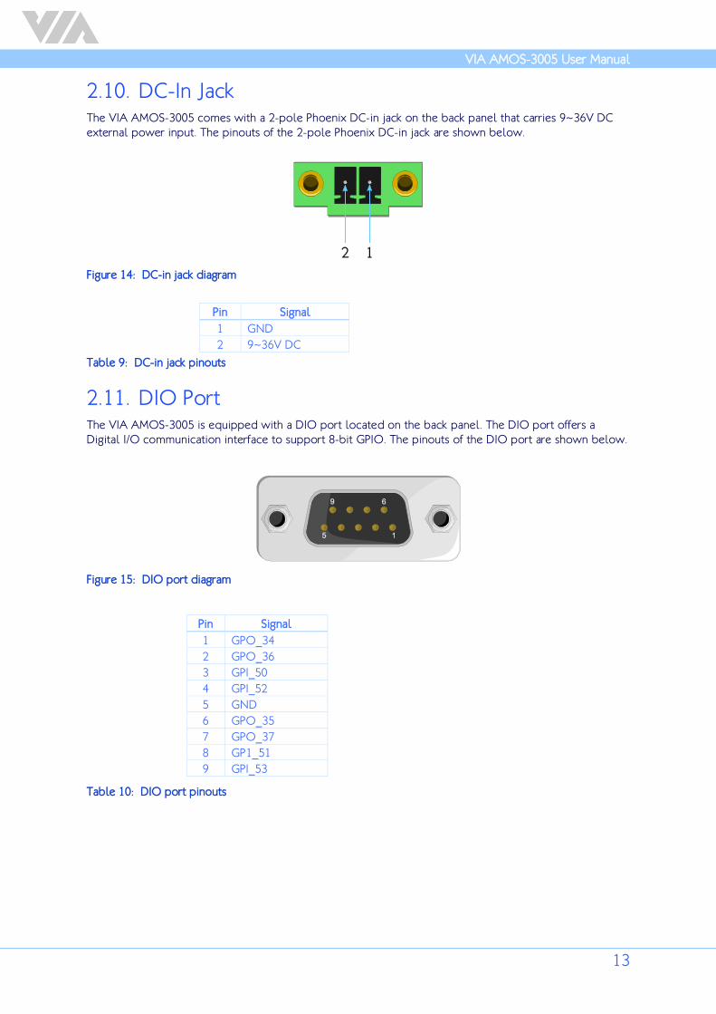
2.10. DC-In Jack The VIA AMOS-3005 comes with a 2-pole Phoenix DC-in jack on the back panel that carries 9~36V DC external power input. The pinouts of the 2-pole Phoenix DC-in jack are shown below.
Figure 14: DC-in jack diagram
Pin Signal 1 GND 2 9~36V DC
Table 9: DC-in jack pinouts
2.11. DIO Port The VIA AMOS-3005 is equipped with a DIO port located on the back panel. The DIO port offers a Digital I/O communication interface to support 8-bit GPIO. The pinouts of the DIO port are shown below.
Figure 15: DIO port diagram
Pin Signal 1 GPO_34 2 GPO_36 3 GPI_50 4 GPI_52 5 GND 6 GPO_35 7 GPO_37 8 GP1_51 9 GPI_53
Table 10: DIO port pinouts

VIA AMOS-3005 User Manual
14
3. Onboard I/O This chapter provides information about the onboard pin headers and connectors on the VIA AMOS-3005.
3.1. USB 2.0 Pin Header The onboard USB 2.0 pin header (JUSB2_1) enables additional two USB 2.0 ports. The pinouts of the USB 2.0 pin header are shown below.
Figure 16: USB 2.0 pin header diagram
Pin Signal Pin Signal 1 VUSB2 2 VUSB2 3 USBD_T3- 4 USBD_T2- 5 USBD_T3+ 6 USBD_T2+ 7 GND 8 GND 9 NC 10 GND
Table 11: USB 2.0 pin header pinouts
VIA AMOS-3005 User Manual
15
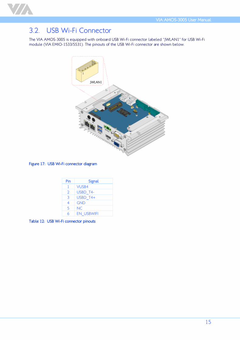
3.2. USB Wi-Fi Connector The VIA AMOS-3005 is equipped with onboard USB Wi-Fi connector labeled “JWLAN1” for USB Wi-Fi module (VIA EMIO-1533/5531). The pinouts of the USB Wi-Fi connector are shown below.
Figure 17: USB Wi-Fi connector diagram
Pin Signal 1 VUSB4 2 USBD_T4- 3 USBD_T4+ 4 GND 5 NC 6 EN_USBWIFI
Table 12: USB Wi-Fi connector pinouts

VIA AMOS-3005 User Manual
16
3.3. MiniPCIe Slot The VIA AMOS-3005 is equipped with miniPCIe slot for wireless networking option such as a 4G, GPS, and Wi-Fi modules. The miniPCIe slot is labeled as “MINIPCIE1”. The location of the miniPCIe slot is shown below.
Figure 18: MiniPCIe slot diagram
3.4. SIM Card Slot The VIA AMOS-3005 comes with SIM card slot that supports 4G SIM card. SIM card usage on the VIA AMOS-3005 requires that a 4G module is installed in the miniPCIe slot, enabling the 4G functionality, otherwise the SIM card slot will be disabled. The SIM card slot is designed for use with 4G modules that do not support built-in SIM card slots. The SIM card slot is labeled as “SIM1”. The location of the SIM card slot is shown below.
Figure 19: SIM card slot diagram

VIA AMOS-3005 User Manual
17
3.5. mSATA Slot The VIA AMOS-3005 comes with an mSATA slot which supports mSATA flash drive module to have a flexible storage. The mSATA slot is labeled as “MSATA”. The location of the mSATA slot is shown below.
Figure 20: mSATA slot diagram
Reminder Please check the bottom side of the mSATA heatsink to make sure there is a black sticker attached on it.

VIA AMOS-3005 User Manual
18
3.6. DDR3 SODIMM Slot The AMOS-3005 comes with one DDR3 SODIMM slot labeled as “SODIMM” that supports non-ECC DDR3 1333 SDRAM SODIMM memory module. The DDR3 SODIMM memory slot can accommodate up to 8GB memory size. The location of the DDR3 SODIMM slot is shown below.
Figure 21: DDR3 SODIMM slot diagram

VIA AMOS-3005 User Manual
19
4. Onboard Jumper Jumper Description A jumper consists of a pair of conductive pins used to close in or bypass an electronic circuit to set up or configure a particular feature using a jumper cap. The jumper cap is a small metal clip covered by plastic. It performs like a connecting bridge to short (connect) the pair of pins. The usual colors of the jumper cap are black/red/blue/white/yellow.
Jumper Setting There are two settings of the jumper pin: “Short and Open”. The pins are “Short” when a jumper cap is placed on the pair of pins. The pins are “Open” if the jumper cap is removed.
In addition, there are jumpers that have three or more pins, and some pins are arranged in series. In case of a jumper with three pins, place the jumper cap on pin 1 and pin 2 or pin 2 and 3 to Short it.
Some jumpers size are small or mounted on a crowded location on the board that makes it difficult to access. Therefore, using a long-nose plier in installing and removing the jumper cap is very helpful.
Figure 22: Jumper settings example
Caution: Make sure to install the jumper cap on the correct pins. Installing it on the wrong pin might cause damage and malfunction.

VIA AMOS-3005 User Manual
20
4.1. COM Voltage Jumpers The COM ports on the front panel can be configured to carry +5V or +12V power, or the Ring Indicator (RI) signal by setting the COM voltage jumpers (JCOMV1 ~ JCOMV2).
4.1.1. JCOMV1 Voltage Jumper The voltage jumper “JCOMV1” is set to determine the input carry voltage or Ring Indicator (RI) signal of COM1 port on the front panel. The control signal Ring Indicator (RI) is the default setting. The jumper settings are shown below.
Figure 23: JCOMV1 voltage jumper diagram
Settings Pin 1 Pin 2 Pin 3 RI (default) Open Open Open +5V Short Short Open +12V Open Short Short
Table 13: JCOMV1 voltage jumper settings

VIA AMOS-3005 User Manual
21
4.1.2. JCOMV2 Voltage Jumper The voltage jumper “JCOMV2” is set to determine the input carry voltage or Ring Indicator (RI) signal of COM2 port on the front panel. The control signal Ring Indicator (RI) is the default setting. The jumper settings are shown below.
Figure 24: JCOMV2 voltage jumper diagram
Settings Pin 1 Pin 2 Pin 3 RI (default) Open Open Open +5V Short Short Open +12V Open Short Short
Table 14: JCOMV2 voltage jumper settings

VIA AMOS-3005 User Manual
22
4.2. USB 2.0 Power Type Jumper The USB 2.0 power type jumper labeled as “JUSB_SEL1” controls the power type delivered to the lockable USB 2.0 ports (USB0 and USB1) on the front panel and to the onboard USB pin header (JUSB2_1). The power can be set either on +5VSUS (Standby power) or +5V. The +5V is the default setting. The jumper settings are shown below
Figure 25: USB 2.0 power type jumper diagram
USB0 and USB1 Settings Pin 1 Pin 3 Pin 5
+5V (default) Short Short Open +5VSUS Open Short Short
JUSB2_1
Settings Pin 2 Pin 4 Pin 6 +5V (default) Short Short Open +5VSUS Open Short Short
Table 15: USB 2.0 power type jumper settings

VIA AMOS-3005 User Manual
23
5. Hardware Installation This chapter provides information about the hardware installation procedures. It is recommended to use a grounded wrist strap before handling computer components. Electrostatic discharge (ESD) can damage some components.
5.1. Installing the DDR3 SODIMM Memory
Step 1
Remove all screws on the front and back panel plates. Then remove the all hex standoff screws of the VGA, DIO and COM ports as shown in the figure below.
Figure 26: Unscrewing the front and back panel plates
Step 2
Gently detach the front and back panel plates from the chassis.
Figure 27: Removing the front and back panel plates
VIA AMOS-3005 User Manual
24
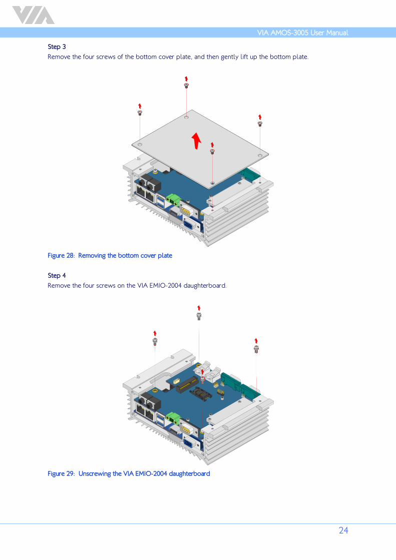
Step 3
Remove the four screws of the bottom cover plate, and then gently lift up the bottom plate.
Figure 28: Removing the bottom cover plate
Step 4
Remove the four screws on the VIA EMIO-2004 daughterboard.
Figure 29: Unscrewing the VIA EMIO-2004 daughterboard

VIA AMOS-3005 User Manual
25
Step 5
Pull up the VIA EMIO-2004 daughterboard to detach it from the mainboard. Slightly incline the daughterboard to the left, then gently pull out the daughterboard rightward.
Figure 30: Removing the VIA EMIO-2004 daughterboard
Step 6
Flip over the VIA EMIO-2004 daughterboard. Peel off the protective (plastic) cover of the pre-installed memory thermal pad on the memory heatsink.
Figure 31: Peeling off the memory thermal pad protective cover

VIA AMOS-3005 User Manual
26
Step 7
Align the notch on the DDR3 SODIMM memory module with the counterpart on the DDR3 SODIMM slot. Then insert the DDR3 SODIMM memory module at a 30° angle.
Figure 32: Installing the DDR3 SODIMM memory module
Step 8
Push down the DDR3 SODIMM memory until the locking clips lock the memory module into place.
Step 9
Reinstall the VIA EMIO-2004 daughterboard.

VIA AMOS-3005 User Manual
27
5.2. Removing the DDR3 SODIMM Memory Step 1
To disengage the locking clips, push the locking clips horizontally outward away from the DDR3 SODIMM memory module.
Figure 33: Disengaging the DDR3 SODIMM locking clips
Step 2
When the locking clips have cleared, the DDR3 SODIMM memory module will automatically pop up. Remove the memory module.
Figure 34: Removing the DDR3 SODIMM memory module

VIA AMOS-3005 User Manual
28
5.3. Installing the mSATA Flash Drive Module
Note: It is highly suggested to use Transcend’s mSATA flash drive module.
Step 1
Prepare the mSATA thermal pad provided in the package.
Step 2
Peel off the bottom protective (plastic) cover of mSATA thermal pad. Paste the thermal pad onto the controller chip on mSATA module.
Figure 35: Installing the mSATA thermal pad
Step 3
Peel off the remaining protective (plastic) cover of the mSATA thermal pad.
Figure 36: Peeling off the protective plastic cover of mSATA thermal pad

VIA AMOS-3005 User Manual
29
Step 4
Flip over the mSATA module. Align the notch on the mSATA module with the counterpart on the mSATA slot. Then insert the module at a 30° angle.
Figure 37: Inserting the mSATA module
Step 5
Once the mSATA module has been fully inserted, push down the module until the screw hole is aligned with the standoff hole. Then secure the module with the provided screw.
Figure 38: Securing the mSATA module
Step 6
Reinstall the VIA EMIO-2004 daughterboard and the bottom plate.

VIA AMOS-3005 User Manual
30
Step 7
Peel off the bottom protective (plastic) cover of the mSATA heatsink thermal pad, and then paste the thermal pad onto the mSATA heatsink.
Figure 39: Installing the mSATA heatsink thermal pad
Step 8
Reinstall the front panel plate. Make sure you remove the remaining protective (plastic) cover of the thermal pad before reinstalling the front panel plate.
Figure 40: Reinstalling the front panel plate

VIA AMOS-3005 User Manual
31
5.4. Reinstalling the VIA EMIO-2004 Daughterboard
Step 1
Slightly incline the VIA EMIO-2004 daughterboard to the left. Gently slide in the daughterboard until the EMIO female connector on the daughterboard is aligned with the EMIO male connector on the VIA EITX-2004 mainboard. Then push down the daughterboard until the EMIO connector is fully connected.
Figure 41: Reinstalling VIA EMIO-2004 daughterboard
Step 2
Secure the VIA EMIO-2004 daughterboard with four screws.
Figure 42: Securing VIA EMIO-2004 daughterboard

VIA AMOS-3005 User Manual
32
5.5. Inserting the SIM Card
Step 1
Firmly push back the SIM card slot to unlock the opening.
Step 2
Pull up the slot and place the SIM card inside. Close the SIM card slot and lock it by sliding back the slot.
Figure 43: Inserting the SIM card

VIA AMOS-3005 User Manual
33
5.6. Installing the Rubber Feet
Step 1
On the bottom side of the VIA AMOS-3005, identify the area where to install the rubber feet.
Step 2
Attach each rubber foot. Firmly press it down to ensure the rubber foot is properly in place.
Figure 44: Installing the rubber feet

VIA AMOS-3005 User Manual
34
5.7. Installing the VIA AMOS-3005 The VIA AMOS-3005 has multiple mounting options. Using the four mounting screws, the VIA AMOS-3005 can be mounted on walls, tables or any suitable flat surfaces. In addition, the VIA AMOS-3005 can be installed behind display monitor using the optional VESA mounting kit.
Reminders: 1. Make sure to remove the rubber feet before mounting the VIA AMOS-3005. The rubber feet are not required when securing the system onto walls or tables. 2. Do not use other types of screws when mounting the VIA AMOS-3005 aside from the provided screws to avoid any damages.
5.7.1. Mounting the VIA AMOS-3005 on Wall/Table
Step 1
Find a suitable surface to mount the VIA AMOS-3005. Drill four holes on flat surface (wall/table). Ensure the diameter of the holes and the distance between the holes are perfectly match with the mounting screws and holes of the VIA AMOS-3005.
Step 2
Install the VIA AMOS-3005 to the wall/table and secure it with the four screws.
Figure 45: Mounting the VIA AMOS-3005

VIA AMOS-3005 User Manual
35
5.7.2. Mounting the VIA AMOS-3005 Behind the Monitor
Step 1
Align the mounting holes of the VESA mounting plate to the available VESA holes of the monitor display.
Step 2
Fasten the VESA mounting plate with four screws at the back of the monitor display.
Figure 46: Installing the VESA mounting plate

VIA AMOS-3005 User Manual
36
Step 3
Install the VIA AMOS-3005 to the VESA mounting plate.
Figure 47: Installing VIA AMOS-3005 to the VESA mounting plate
Step 4
Connect all the necessary cables.

VIA AMOS-3005 User Manual
37
6. BIOS Setup This chapter gives a detailed explanation of the BIOS setup functions.
6.1. Entering the BIOS Setup Utility Power on the computer and press Delete during the beginning of the boot sequence to enter the BIOS Setup Utility. If the entry point has passed, restart the system and try again.
6.2. Control Keys Up Move up one row
Down Move down one row
Left Move to the left in the navigation bar
Right Move to the right in the navigation bar
Enter Access the highlighted item / Select the item
Esc Jumps to the Exit screen or returns to the previous screen
+1 Increase the numeric value
-1 Decrease the numeric value
F1 General help2
F2 Previous value
F3 Load optimized defaults
F4 Save all the changes and exit
Notes: 1. Must be pressed using the 10-key pad. 2. The General help contents are only for the Status Page and Option Page setup menus.
6.3. Getting Help The BIOS Setup Utility provides a “General Help” screen. This screen can be accessed at any time by pressing F1. The help screen displays the keys for using and navigating the BIOS Setup Utility. Press Esc to exit the help screen.

VIA AMOS-3005 User Manual
38
6.4. System Overview The System Overview screen is the default screen that is shown when the BIOS Setup Utility is launched. This screen can be accessed by traversing the navigation bar to the “Main” label.
Figure 48: Illustration of the Main menu screen
6.4.1. BIOS Information The content in this section of the screen shows the information about the vendor, the Core version, UEFI specification version, the project version and date & time of the project build.
6.4.2. Memory Information This section shows the amount of memory that is installed on the hardware platform.
6.4.3. System Language This option allows the user to configure the language that the user wants to use.
6.4.4. System Date This section shows the current system date. Press Tab to traverse right and Shift+Tab to traverse left through the month, day, and year segments. The + and - keys on the number pad can be used to change the values. The weekday name is automatically updated when the date is altered. The date format is [Weekday, Month, Day, Year].
6.4.5. System Time This section shows the current system time. Press Tab to traverse right and Shift+Tab to traverse left through the hour, minute, and second segments. The + and - keys on the number pad can be used to change the values. The time format is [Hour : Minute : Second].

VIA AMOS-3005 User Manual
39
6.5. Advanced Settings The Advanced Settings screen shows a list of categories that can provide access to a sub-screen. Sub-screen links can be identified by the preceding right-facing arrowhead.
Figure 49: Illustration of the Advanced Settings screen
The Advanced Settings screen contains the following links:
• ACPI Settings
• S5 RTC Wake Settings
• CPU Configuration
• SATA Configuration
• USB Configuration
• F71869 Super IO Configuration
• F71869 H/W Monitor
• Clock Generator Configuration

VIA AMOS-3005 User Manual
40
6.5.1. ACPI Settings ACPI grants the operating system direct control over system power management. The ACPI Configuration screen can be used to set a number of power management related functions.
Figure 50: Illustration of the ACPI Settings screen
6.5.1.1. Enable Hibernation Enable/disable system ability to Hibernate.
6.5.1.2. ACPI Sleep State Except when selecting “Suspend Disabled”, the system will enter into the corresponding sleep state when the Power button (configured as Standby / Sleep) is pressed or go to Standby / Sleep when the system is running under ACPI OS.

VIA AMOS-3005 User Manual
41
6.5.2. S5 RTC Wake Settings The S5 RTC Wake Settings screen enables system to wake from S5 using RTC alarm
Figure 51: Illustration of the S5 RTC Wake Settings screen
6.5.2.1. Wake system with Fixed Time Enable or disable system wake on alarm event. When enabled, system will wake on the date/ hr:min:sec specified. “0” means everyday.
6.5.2.2. Wake system with Dynamic Time Enable or disable system wake on alarm event. When enabled, system will wake on the current time + Increase minutes. Available options are 1 – 5.

VIA AMOS-3005 User Manual
42
6.5.3. CPU Configuration The CPU Configuration screen shows detailed information about the built-in processor.
Figure 52: Illustration of the CPU Configuration screen

VIA AMOS-3005 User Manual
43
6.5.4. SATA Configuration The SATA Configuration screen allows the user to view and configure the SATA configuration settings.
Figure 53: Illustration of the SATA Configuration screen
6.5.4.1. SATA Mode This option allows the user to manually configure SATA controller for a particular mode.
IDE Mode Set this value to change the SATA to IDE mode.
AHCI Mode Set this value to change the SATA to AHCI mode.
VIA AMOS-3005 User Manual
44
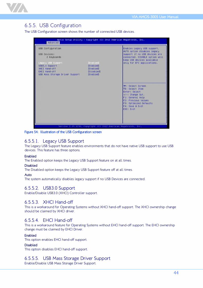
6.5.5. USB Configuration The USB Configuration screen shows the number of connected USB devices.
Figure 54: Illustration of the USB Configuration screen
6.5.5.1. Legacy USB Support The Legacy USB Support feature enables environments that do not have native USB support to use USB devices. This feature has three options.
Enabled The Enabled option keeps the Legacy USB Support feature on at all times.
Disabled The Disabled option keeps the Legacy USB Support feature off at all times.
Auto The system automatically disables legacy support if no USB Devices are connected.
6.5.5.2. USB3.0 Support Enable/Disable USB3.0 (XHCI) Controller support.
6.5.5.3. XHCI Hand-off This is a workaround for Operating Systems without XHCI hand-off support. The XHCI ownership change should be claimed by XHCI driver.
6.5.5.4. EHCI Hand-off This is a workaround feature for Operating Systems without EHCI hand-off support. The EHCI ownership change must be claimed by EHCI Driver.
Enabled This option enables EHCI hand-off support.
Disabled This option disables EHCI hand-off support.
6.5.5.5. USB Mass Storage Driver Support Enable/Disable USB Mass Storage Driver Support.

VIA AMOS-3005 User Manual
45
6.5.6. F71869 Super IO Configuration The F71869 Super IO Configuration screen allows the user to set system Super IO Chip parameters.
Figure 55: Illustration of the F71869 Super IO Configuration screen
6.5.6.1. Serial Port 1 Configuration Set parameters of Serial Port 1 (COM1).
6.5.6.1.1. Serial Port Enable or Disable Serial Port (COM).
6.5.6.1.2. Uart Transmission Mode Change the serial port transmission mode. This feature has 3 options: RS232/RS422/RS485.
6.5.6.2. Serial Port 2 Configuration Set parameters of Serial Port 2 (COM2).
6.5.6.2.1. Serial Port Enable or Disable Serial Port (COM).
6.5.6.2.2. Uart Transmission Mode Change the serial port transmission mode. This feature has 3 options: RS232/RS422/RS485.

VIA AMOS-3005 User Manual
46
6.5.7. F71869 H/W Monitor F71869 screen shows F71869 H/W Monitor status.
Figure 56: Illustration of the F71869 H/W Monitor

VIA AMOS-3005 User Manual
47
6.5.8. Clock Generator Configuration The Clock Generator Configuration screen enables access to the Spread Spectrum Setting feature.
Figure 57: Illustration of the Clock Generator Configuration screen
6.5.8.1. CPU Spread Spectrum The Spread Spectrum Setting feature enables the BIOS to modulate the clock frequencies originating from the mainboard. The settings are in percentages of modulation. Higher percentages result in greater modulation of clock frequencies. This feature has 3 options: Disabled, +-0.25% and -0.5%.
6.5.8.2. PCIe Spread Spectrum Select PCIe Spread Spectrum. This feature has 2 options: Disabled and -0.5%.

VIA AMOS-3005 User Manual
48
6.6. Chipset Settings The Chipset Settings screen shows a list of categories that can provide access to a sub-screen. Sub-screen links can be identified by the preceding right-facing arrowhead.
Figure 58: Illustration of the Chipset Settings screen
The Chipset Settings screen contains the following links:
• DRAM Configuration
• Video Configuration
• PMU-ACPI Configuration
• HDAC Configuration
• Others Configuration

VIA AMOS-3005 User Manual
49
6.6.1. DRAM Configuration The DRAM Configuration screen has two features for controlling the system DRAM. All other DRAM features are automated and cannot be accessed.
Figure 59: Illustration of the DRAM Configuration screen
6.6.1.1. DRAM Clock The DRAM Clock option enables the user to determine how the BIOS handles the memory clock frequency. The memory clock can either be dynamic or static. This feature has eleven options.
By SPD By SPD option enables the BIOS to select a compatible clock frequency for the installed memory.
400MHz The 400MHz option forces the BIOS to be fixed at 800MHz for DDR3 memory modules.
533MHz The 533MHz option forces the BIOS to be fixed at 1066MHz for DDR3 memory modules.
667MHz The 667MHz option forces the BIOS to be fixed at 1334MHz for DDR3 memory modules.
6.6.1.2. VGA Share Memory (Frame Buffer) The VGA Share Memory feature enables the user to choose the amount of the system memory to reserve for use by the integrated graphics controller. The selections of memory amount that can be reserved are 256MB and 512MB.

VIA AMOS-3005 User Manual
50
6.6.2. Video Configuration The Video Configuration screen has features for controlling the integrated graphics controller in the VX11 chipset.
Figure 60: Illustration of the Video Configuration screen
6.6.2.1. Select Display Device Control Select VX11 Display Device Control. Available options are: Auto and Manual.
6.6.2.2. Select Display Device 1 and 2 The Select Display Device feature enables the user to choose a specific display interface. This feature has two options: CRT and HDMI. If both Select Display Device 1 and Select Display Device 2 are set to the same interface, then any display device connected to the other interface will not function. For example, if both Select Display 1 and 2 are set to CRT, then no data will be sent to the HDMI port.

VIA AMOS-3005 User Manual
51
6.6.3. PMU_ACPI Configuration The PMU_ACPI Configuration screen can be used to set a number of power management related functions.
Figure 61: Illustration of the PMU_ACPI Configuration screen
6.6.3.1. AC Loss Auto-restart AC Loss Auto-restart defines how the system will respond after AC power has been interrupted while the system is on. There are three options.
Power Off The Power Off option keeps the system in an off state until the power button is pressed again.
Power On The Power On option restarts the system when the power has returned.
Last State The Last State option restores the system to its previous state when the power was interrupted.
6.6.3.2. USB S4 WakeUp The USB S4 WakeUp enables the system to resume through the USB device port from S4 state. There are two options: “Enabled” and “Disabled”.

VIA AMOS-3005 User Manual
52
6.6.4. HDAC Configuration HDAC Configuration Parameters.
Figure 62: Illustration of the HDAC Configuration screen
6.6.4.1. OnChip HDAC Device This feature has 2 options: Enable or Disable HDAC Control.

VIA AMOS-3005 User Manual
53
6.6.5. Others Configuration The Others Configuration screen can be used to set Watchdog Timer Configuration.
Figure 63: Illustration of the Others Configuration screen
6.6.5.1. WATCHDOG Timer Enable The WATCHDOG Timer Enable feature unlocks three other features that enable the BIOS to monitor the state of the system. This feature has two options: enabled or disabled.
6.6.5.2. WATCHDOG Timer RUN/STOP The WATCHDOG Timer RUN/STOP feature controls if the WATCHDOG timer is active or dormant. This feature has two options: stop and run.
6.6.5.3. WATCHDOG Timer ACTION The WATCHDOG Timer ACTION feature determines the action the WATCHDOG timer should take if the timer counts down to zero. This feature has two options: reset and power off.
6.6.5.4. WATCHDOG Timer COUNT The WATCHDOG Timer COUNT feature determines the length of time the timer should count when the timer is first triggered. This feature has four options: 72, 389, 706, and 1023 seconds.

VIA AMOS-3005 User Manual
54
6.7. Boot Settings The Boot Settings screen has a single link that goes to the Boot Configuration and Boot Option Priorities screens.
Figure 64: Illustration of the Boot Settings screen
6.7.1. Boot Configuration The Boot Settings Configuration screen has several features that can be run during the system boot sequence.
6.7.1.1. Setup Prompt Timeout Number of seconds to wait for setup activation key. 65535(0xFFFF) means indefinite waiting.
6.7.1.2. BootupNumLock State Select the keyboard NumLock state from On and Off.
6.7.1.3. Display Logo The Display Logo feature hides all of the Power-on Self Test (POST) messages during the boot sequence. Instead of the POST messages, the user will see an OEM logo. This feature has two options: enabled and disabled.
6.7.2. Boot Option Priorities The Boot Option Priorities screen lists all bootable devices.
6.7.2.1. Launch PXE OpROM policy Do not launch Prevent the option for Legacy Network Device.
Legacy only Allow the option for Legacy Network Device.

VIA AMOS-3005 User Manual
55
6.8. Security Settings The Security Settings screen provides a way to restrict access to the BIOS or even the entire system.
Figure 65: Illustration of the Security Settings screen
6.8.1. Security Settings
6.8.1.1. Administrator Password/User Password This option is for setting a password for accessing the BIOS setup utility. When a password has been set, a password prompt will be displayed whenever the BIOS setup utility is launched. This prevents an unauthorized person from changing any part of the system configuration.
When a supervisor password is set, the Password Check option will be unlocked.

VIA AMOS-3005 User Manual
56
6.9. Save & Exit The Save & Exit Configuration screen has the following features:
Figure 66: Illustration of the Save & Exit screen
6.9.1. Save Changes and Exit Save all changes to the BIOS and exit the BIOS Setup Utility. The “F4” hotkey can also be used to trigger this command.
6.9.2. Discard Changes and Exit Exit the BIOS Setup Utility without saving any changes. The “Esc” hotkey can also be used to trigger this command.
6.9.3. Save Changes and Reset Save all changes to the BIOS and reboot the system. The new system configuration parameters will take effect.
6.9.4. Discard Changes and Reset This command reverts all changes to the settings that were in place when the BIOS Setup Utility was launched.
Save Options
6.9.5. Save Changes Save Changes done so far to any of the setup options.
6.9.6. Discard Changes This command reverts all changes to the settings that were in place when the BIOS Setup Utility was launched.
VIA AMOS-3005 User Manual
57
Restore Default
6.9.7. Save as User Defaults Save the changes done so far as User Defaults.
6.9.8. Restore User Defaults Restore the User Defaults to all the setup options.
Boot Override
Launch EFI Shell from filesystem device

VIA AMOS-3005 User Manual
58
7. Software and Technical Support
7.1. Windows and Linux Support The VIA AMOS-3005 is fully compatible with Windows and Linux operating systems.
7.1.1. Driver Installation The latest drivers can be downloaded from the VIA website at www.viatech.com
7.2. Technical Support and Assistance • For utilities downloads, latest documentation and new information about the VIA AMOS-3005, go
to http://www.viatech.com/en/systems/industrial-fanless-pcs/AMOS-3005
• For technical support and additional assistance, always contact your local sales representative or system distributor, or go to https://www.viatech.com/en/support/technical-support/ to fill up the form request.
• For OEM clients and system integrators developing a product for long term production, other code and resources may also be made available. Please visit our website at https://www.viatech.com/en/about/contact/ to submit a request.

VIA AMOS-3005 User Manual
59
Appendix A. Installing Wireless Accessories This chapter provides you with information on how to install the VIA EMIO wireless module into the VIA AMOS-3005. It is recommended to use a grounded wrist strap before handling computer components. Electrostatic discharge (ESD) can damage some components.
A.1. Installing the VIA EMIO MiniPCIe Module Step 1
Align the notch on the VIA EMIO miniPCIe module (VIA EMIO-2531/2551/2573) with its counterpart on the miniPCIe slot on the daughterboard (VIA EMIO-2004). Then insert the module at a 30° angle.
Figure 67: Inserting the VIA EMIO miniPCIe module
Step 2
Once the module has been fully inserted, push down the module until the screw hole align with the standoff hole, and then secure the module with the provided screw.
Figure 68: Securing the VIA EMIO miniPCIe module

VIA AMOS-3005 User Manual
60
Step 3
Remove the antenna hole cover from the front panel plate. To facilitate removing the cover, use a pair of needle-nose pliers to depress both locking clips simultaneously.
Figure 69: Removing the 4G antenna hole cover
Figure 70: Removing the GPS antenna hole cover
Figure 71: Removing the Wi-Fi antenna hole cover

VIA AMOS-3005 User Manual
61
Step 4
Insert the 4G/GPS/Wi-Fi antenna cable into the antenna hole from inside of the front panel plate. Insert the washer, fasten it with the nut, and install the external antenna. Insert the other end of the antenna cable into the available space going down to the bottom side of the system. Stretchout the cable to reach the installed VIA EMIO miniPCIe module. Then reinstall the front panel plate.
Figure 72: Installing the 4G antenna cable and antenna
Figure 73: Installing the GPS antenna cable and antenna

VIA AMOS-3005 User Manual
62
Figure 74: Installing the Wi-Fi antenna cable and antenna
Step 5
Connect the other end of the 4G/GPS/Wi-Fi antenna cable to the micro-RF connector on the VIA EMIO miniPCIe module.
Figure 75: Connecting the 4G/GPS/Wi-Fi antenna cable to VIA EMIO miniPCIe module

VIA AMOS-3005 User Manual
63
A.2. Installing the VIA EMIO USB Wi-Fi Module Step 1
Mount the VIA EMIO USB Wi-Fi module (VIA EMIO-1533/5531) on the daughterboard (VIA EMIO-2004). Align the module’s mounting holes with the standoff screw holes on the daughterboard then secure it with two screws.
Figure 76: Installing the VIA EMIO USB Wi-Fi module
Step 2
Connect the USB Wi-Fi cable to the connector on VIA EMIO USB Wi-Fi module, and then attach the other end of the cable to the onboard USB Wi-Fi connector (JWLAN1) on the VIA EMIO-2004 daughterboard.
Figure 77: Connecting the USB Wi-Fi cable

VIA AMOS-3005 User Manual
64
Step 3
Remove the Wi-Fi antenna hole cover from the front panel plate. To facilitate removing the cover, use a pair of needle-nose pliers to depress both locking clips simultaneously.
Figure 78: Removing the Wi-Fi antenna hole cover
Step 4
Insert the Wi-Fi antenna cable into the antenna hole from inside of the front panel plate. Insert the washer, fasten it with the nut, and install the external antenna. Pull the other end of the antenna cable and insert it to the available space going down to the bottom side of the system. Stretchout the cable to reach the installed VIA EMIO USB Wi-Fi module. Then reinstall the front panel plate.
Figure 79: Installing the Wi-Fi antenna

VIA AMOS-3005 User Manual
65
Step 5
Connect the other end of the Wi-Fi antenna cable to the micro-RF connector labeled as “MAIN” on the VIA EMIO USB Wi-Fi module.
Figure 80: Connecting the Wi-Fi antenna cable to VIA EMIO USB Wi-Fi module
Step 6
Reinstall the back panel and bottom cover plates.

1F, 531 Zhong-zheng Road,Xindian Dist., New Taipei City 231Taiwan
Tel: 886-2-2218-5452Fax: 886-2-2218-9860Email: [email protected]
940 Mission CourtFremont, CA 94539,USA
Tel: 1-510-687-4688Fax: 1-510-687-4654Email: [email protected]
Email: [email protected]
Taiwan Headquarters USA
Europe
Tsinghua Science Park Bldg. 7No. 1 Zongguancun East Road,Haidian Dist., Beijing, 100084China
Tel: 86-10-59852288Fax: 86-10-59852299Email: [email protected]
3-15-7 Ebisu MT Bldg. 6F,Higashi, Shibuya-kuTokyo 150-0011Japan
Tel: 81-3-5466-1637Fax: 81-3-5466-1638Email: [email protected]
ChinaJapan