USB Peripheral Controller with SPI Interfacefelber/DataSheets/USB/MAX3420E.pdfUSB Peripheral...
23
General Description The MAX3420E contains the digital logic and analog circuitry necessary to implement a full-speed USB peripheral compliant to USB specification rev 2.0. A built-in full-speed transceiver features ±15kV ESD pro- tection and programmable USB connect and discon- nect. An internal SIE (serial-interface engine) handles low-level USB protocol details such as error checking and bus retries. The MAX3420E operates using a regis- ter set accessed by an SPI interface that operates up to 26MHz. Any SPI master (microprocessor, ASIC, DSP, etc.) can add USB functionality using the simple 3- or 4-wire SPI interface. Internal level translators allow the SPI interface to run at a system voltage between 1.71V and 3.6V. USB timed operations are done inside the MAX3420E with inter- rupts provided at completion so an SPI master does not need timers to meet USB timing requirements. The MAX3420E includes four general-purpose inputs and outputs so any microprocessor that uses I/O pins to implement the SPI interface can reclaim the I/O pins and gain additional ones. The MAX3420E operates over the extended -40°C to +85°C temperature range and is available in a 32-pin TQFP package (7mm x 7mm) and a space-saving 24- pin TQFN package (4mm x 4mm). Applications Features ♦ Microprocessor-Independent USB Solution ♦ Complies with USB Specification Revision 2.0 (Full-Speed Operation) ♦ Integrated Full-Speed USB Transceiver ♦ Firmware/Hardware Control of an Internal D+ Pullup Resistor ♦ Programmable 3- or 4-Wire 26MHz SPI Interface ♦ Level Translators and V L Input Allow Independent System Interface Voltage ♦ Internal Comparator Detects V BUS for Self-Powered Applications ♦ ESD Protection on D+, D-, and VBCOMP ♦ Interrupt Output Pin (Level or Programmable Edge) Allows Polled or Interrupt-Driven SPI Interface ♦ Intelligent USB Serial Interface Engine (SIE) Automatically Handles USB Flow Control and Double Buffering Handles Low-Level USB Signaling Details Contains Timers for USB Time-Sensitive Operations So SPI Master Does Not Need to Time Events ♦ Built-In Endpoint FIFOs: EP0: CONTROL (64 Bytes) EP1: OUT, Bulk or Interrupt, 2 x 64 Bytes (Double-Buffered) EP2: IN, Bulk or Interrupt, 2 x 64 Bytes (Double-Buffered) EP3: IN, Bulk or Interrupt (64 Bytes) ♦ Double-Buffered Data Endpoints Increase Throughput by Allowing the SPI Master to Transfer Data Concurrently with USB Transfers Over the Same Endpoint ♦ SETUP Data Has Its Own 8-Byte FIFO, Simplifying Firmware ♦ Four General-Purpose Inputs and Four General- Purpose Outputs ♦ Space-Saving TQFP and TQFN Packages MAX3420E USB Peripheral Controller with SPI Interface ________________________________________________________________ Maxim Integrated Products 1 19-3781; Rev 0; 8/05 For pricing, delivery, and ordering information, please contact Maxim/Dallas Direct! at 1-888-629-4642, or visit Maxim’s website at www.maxim-ic.com. Cell Phones PC Peripherals Microprocessors and DSPs Custom USB Devices Cameras Desktop Routers PLCs Set-Top Boxes PDAs MP3 Players Instrumentation PART TEMP RANGE PIN- PACKAGE PACKAGE CODE MAX3420EECJ -40°C to +85°C 32 TQFP 7mm x 7mm x 1.4mm C32-1 MAX3420EETG* -40°C to +85°C 24 TQFN 4mm x 4mm x 0.8mm T2444-4 Ordering Information *Future product—contact factory for availability.
Transcript of USB Peripheral Controller with SPI Interfacefelber/DataSheets/USB/MAX3420E.pdfUSB Peripheral...

General DescriptionThe MAX3420E contains the digital logic and analogcircuitry necessary to implement a full-speed USBperipheral compliant to USB specification rev 2.0. Abuilt-in full-speed transceiver features ±15kV ESD pro-tection and programmable USB connect and discon-nect. An internal SIE (serial-interface engine) handleslow-level USB protocol details such as error checkingand bus retries. The MAX3420E operates using a regis-ter set accessed by an SPI interface that operates up to26MHz. Any SPI master (microprocessor, ASIC, DSP,etc.) can add USB functionality using the simple 3- or4-wire SPI interface.
Internal level translators allow the SPI interface to run ata system voltage between 1.71V and 3.6V. USB timedoperations are done inside the MAX3420E with inter-rupts provided at completion so an SPI master does notneed timers to meet USB timing requirements. TheMAX3420E includes four general-purpose inputs andoutputs so any microprocessor that uses I/O pins toimplement the SPI interface can reclaim the I/O pinsand gain additional ones.
The MAX3420E operates over the extended -40°C to+85°C temperature range and is available in a 32-pinTQFP package (7mm x 7mm) and a space-saving 24-pin TQFN package (4mm x 4mm).
Applications
Features♦ Microprocessor-Independent USB Solution
♦ Complies with USB Specification Revision 2.0(Full-Speed Operation)
♦ Integrated Full-Speed USB Transceiver
♦ Firmware/Hardware Control of an Internal D+Pullup Resistor
♦ Programmable 3- or 4-Wire 26MHz SPI Interface
♦ Level Translators and VL Input Allow IndependentSystem Interface Voltage
♦ Internal Comparator Detects VBUS for Self-Powered Applications
♦ ESD Protection on D+, D-, and VBCOMP♦ Interrupt Output Pin (Level or Programmable
Edge) Allows Polled or Interrupt-Driven SPIInterface
♦ Intelligent USB Serial Interface Engine (SIE)Automatically Handles USB Flow Control andDouble Buffering
Handles Low-Level USB Signaling Details
Contains Timers for USB Time-SensitiveOperations So SPI Master Does Not Need toTime Events
♦ Built-In Endpoint FIFOs:EP0: CONTROL (64 Bytes)
EP1: OUT, Bulk or Interrupt, 2 x 64 Bytes (Double-Buffered)
EP2: IN, Bulk or Interrupt, 2 x 64 Bytes (Double-Buffered)
EP3: IN, Bulk or Interrupt (64 Bytes)
♦ Double-Buffered Data Endpoints IncreaseThroughput by Allowing the SPI Master toTransfer Data Concurrently with USB TransfersOver the Same Endpoint
♦ SETUP Data Has Its Own 8-Byte FIFO, SimplifyingFirmware
♦ Four General-Purpose Inputs and Four General-Purpose Outputs
♦ Space-Saving TQFP and TQFN Packages
MA
X3
42
0E
USB Peripheral Controllerwith SPI Interface
________________________________________________________________ Maxim Integrated Products 1
19-3781; Rev 0; 8/05
For pricing, delivery, and ordering information, please contact Maxim/Dallas Direct! at 1-888-629-4642, or visit Maxim’s website at www.maxim-ic.com.
Cell PhonesPC PeripheralsMicroprocessors andDSPsCustom USB DevicesCamerasDesktop Routers
PLCsSet-Top BoxesPDAsMP3 PlayersInstrumentation
PART TEMP RANGEPIN-PACKAGE
PACKAGECODE
M AX 3420E E C J - 40°C to + 85°C 32 TQFP 7m m x 7m m x1.4m m
C 32- 1
M AX 3420E E TG* - 40°C to + 85°C 24 TQFN 4m m x 4m m x0.8m m
T2444- 4
Ordering Information
*Future product—contact factory for availability.
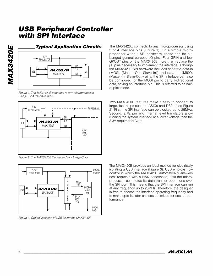
The MAX3420E connects to any microprocessor using3 or 4 interface pins (Figure 1). On a simple micro-processor without SPI hardware, these can be bit-banged general-purpose I/O pins. Four GPIN and fourGPOUT pins on the MAX3420E more than replace theµP pins necessary to implement the interface. Althoughthe MAX3420E SPI hardware includes separate data-in(MOSI, (Master-Out, Slave-In)) and data-out (MISO,(Master-In, Slave-Out)) pins, the SPI interface can alsobe configured for the MOSI pin to carry bidirectionaldata, saving an interface pin. This is referred to as half-duplex mode.
Two MAX3420E features make it easy to connect tolarge, fast chips such as ASICs and DSPs (see Figure2). First, the SPI interface can be clocked up to 26MHz.Second, a VL pin and internal level translators allowrunning the system interface at a lower voltage than the3.3V required for VCC.
The MAX3420E provides an ideal method for electricallyisolating a USB interface (Figure 3). USB employs flowcontrol in which the MAX3420E automatically answershost requests with a NAK handshake, until the micro-processor completes its data-transfer operations overthe SPI port. This means that the SPI interface can runat any frequency up to 26MHz. Therefore, the designeris free to choose the interface operating frequency andto make opto-isolator choices optimized for cost or per-formance.
MA
X3
42
0E
USB Peripheral Controllerwith SPI Interface
2 _______________________________________________________________________________________
Typical Application Circuits
3.3VREGULATOR
SPI3, 4
INTUSB µP
MAX3420E
3.3VREGULATOR
POWER RAIL
ASIC,DSP,ETC.
SPI3, 4
INTMAX3420EUSB
Figure 2. The MAX3420E Connected to a Large Chip
3.3VREGULATOR
MISO
LOCALGND
LOCALPOWER
INT
MAX3420ESCLKMOSI
SS
MICROASICDSP
ISOLATORS
USB
Figure 3. Optical Isolation of USB Using the MAX3420E
Figure 1. The MAX3420E connects to any microprocessorusing 3 or 4 interface pins.
MA
X3
42
0E
USB Peripheral Controllerwith SPI Interface
_______________________________________________________________________________________ 3
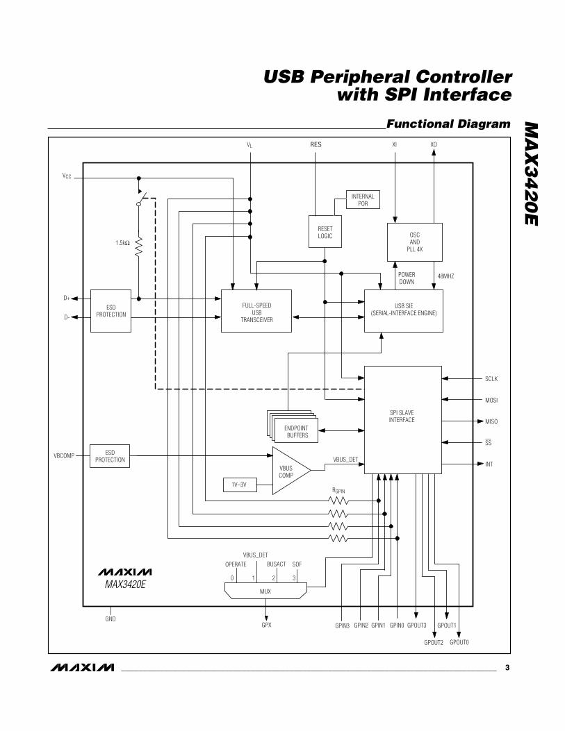
Functional Diagram
GPIN3
RGPIN1V–3V
VBCOMP
D-
D+
VCC
GPIN2 GPIN1 GPIN0 GPOUT3
GPOUT2
GPOUT1
GPOUT0
VBUSCOMP
SS
MISO
SCLK
INT
SPI SLAVEINTERFACE
USB SIE(SERIAL-INTERFACE ENGINE)
FULL-SPEEDUSB
TRANSCEIVER
RESETLOGIC
1.5kΩ
INTERNALPOR
RES XIVL XO
POWERDOWN
OSCAND
PLL 4X
48MHZ
ESDPROTECTION
ESDPROTECTION
GPX
VBUS_DETOPERATE SOFBUSACT
MUX
0 1 2 3
MOSI
VBUS_DET
ENDPOINTBUFFERS
MAX3420E
GND
MA
X3
42
0E
USB Peripheral Controllerwith SPI Interface
4 _______________________________________________________________________________________
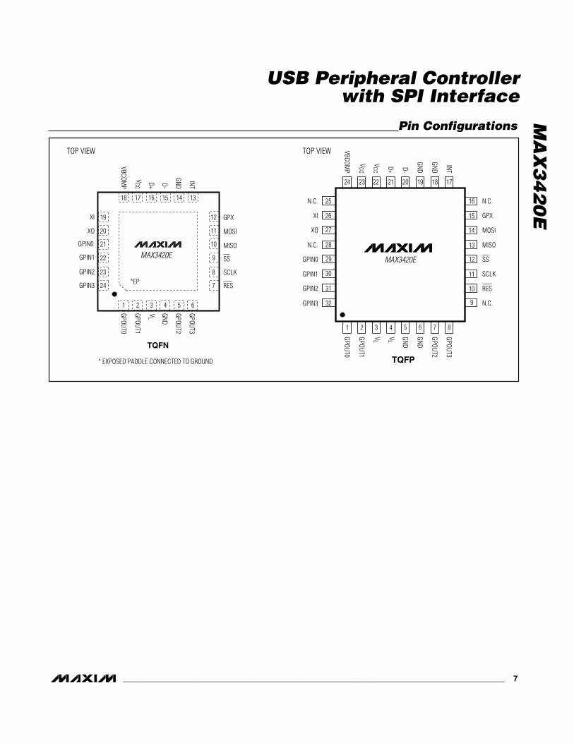
Pin DescriptionPIN
TQFN TQFPNAME
INPUT/OUTPUT
FUNCTION
1 1 GPOUT0
2 2 GPOUT1Output
G ener al - P ur p ose P ush- P ul l O utp uts. G P OU T3–G P OU T0 l og i c l evel s ar e r efer enced to the vol tag e on V L . The S P I m aster contr ol s the G P OU T3–GP OU T0 states b yw r i ti ng to b i t 3 thr oug h b i t 0 of the IOP IN S ( R20) r eg i ster .
3 3, 4 VL InputLevel-Translator Reference Voltage. Connect VL to the system’s 1.71V to 3.6Vlogic-level power supply. Bypass VL to ground with a 0.1µF capacitor as close tothe VL pin as possible.
4, 14 5, 6, 18, 19 GND Input Ground
5 7 GPOUT2
6 8 GPOUT3Output
Gener al - P ur p ose P ush- P ul l O utp uts. GP OU T3–GP O U T0 l og i c l evel s ar e r efer enced tothe vol tag e on V L. The S P I m aster contr ol s the GP O U T3–GP OU T0 states b y w r i ti ng tob i t 3 thr oug h b i t 0 of the IOP IN S ( R20) r eg i ster .
7 10 RES InputDevice Reset. Drive RES low to clear all of the internal registers except forPINCTL (R17), USBCTL (R15), and SPI logic. See the Device Reset section for adescription of resets available on the MAX3420E.
8 11 SCLK Input
SPI Serial-Clock Input. An external SPI master supplies this clock with frequenciesup to 26MHz. The logic level is referenced to the voltage on VL. Data is clockedinto the SPI slave interface on the positive edge of SCLK. Data is clocked out ofthe SPI slave interface on the falling edge of SCLK.
9 12 SS Input
SPI Slave-Select Input. The SS logic level is referenced to the voltage on VL.When SS is driven high, the SPI slave interface is not selected and SCLKtransitions are ignored. An SPI transfer begins with a high-to-low SS transition andends with a low-to-high SS transition. The MAX3420E SS pin is sensitive toundershoot. A 33pF capacitor should be connected from SS to ground to preventany noise spikes.*
10 13 MISO OutputSPI Serial-Data Output (Master-In, Slave-Out). MISO is a push-pull output. MISO istri-stated in half-duplex mode or when SS = 1. The MISO logic level is referencedto the voltage on VL.
11 14 MOSIInput orInput/Output
SPI Serial-Data Input (Master-Out, Slave-In). The logic level on MOSI isreferenced to the voltage on VL. MOSI can also be configured as a bidirectionalMOSI/MISO input and output.
12 15 GPX Output
General-Purpose Multiplexed Output. The internal MAX3420E signal that appearson GPX is programmable by writing to the GPXB and GPXA bits of the PINCTL(R17) register. GPX indicates one of four signals: OPERATE (00, Default),VBUS_DET (01), BUSACT (10), and SOF (11).
13 17 INT Output
Inter r up t Outp ut. In ed g e m od e, the l og i c l evel on IN T i s r efer enced to the vol tag eon V L. In ed g e m od e , IN T i s a p ush- p ul l outp ut w i th p r og r am m ab l e p ol ar i ty. In l evel m od e, IN T i s op en d r ai n and acti ve l ow . S et the IE b i t i n the C P U C TL ( R16) r eg i ster toenab l e IN T.
15 20 D-Input/Output
U S B D - S i g nal . C onnect D - to a U S B “B” connector thr ough a 33Ω ( ±1%) ser ies resi stor .
*33pF capacitor will not be required after redesign.

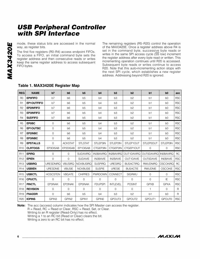
Register DescriptionThe SPI master controls the MAX3420E by reading andwriting 21 registers (Table 1). For a complete descrip-tion of register contents, please refer to the “MAX3420EProgramming Guide.” A register access consists of theSPI master first writing an SPI command byte, followedby reading or writing the contents of the addressedregister. All SPI transfers are MSB (most significant bit)first. The command byte contains the register address,a direction bit (Read = 0, Write = 1), and the ACKSTATbit (Figure 4). The SPI master addresses theMAX3420E registers by writing the binary value of theregister number in the Reg4 through Reg0 bits of thecommand byte. For example, to access the IOPINS
(R20) register, the Reg4 through Reg0 bits would be asfollows: Reg4 = 1, Reg3 = 0, Reg2 = 1, Reg1 = 0, Reg0= 0. The DIR (direction) bit determines the direction forthe data transfer. DIR = 1 means the data byte(s) willbe written to the register, and DIR = 0 means the databyte(s) will be read from the register. The ACKSTAT bitsets the ACKSTAT bit in the EPSTALLS (R9) register.The SPI master sets this bit to indicate that it has fin-ished servicing a CONTROL transfer. Since the bit isfrequently used, having it in the SPI command byteimproves firmware efficiency. In SPI full-duplex mode,the MAX3420E clocks out eight USB status bits as thecommand byte is clocked in (Figure 5). In half-duplex
MA
X3
42
0E
USB Peripheral Controllerwith SPI Interface
_______________________________________________________________________________________ 5
Pin Description (continued)
PIN
TQFN TQFPNAME
INPUT/OUTPUT
FUNCTION
16 21 D+Input/Output
USB D+ Signal. Connect D+ to a USB “B” connector through a 33Ω (±1%)series resistor. The 1.5kΩ D+ pullup resistor is internal to the device.
17 22, 23 VCC InputUSB Transceiver Power-Supply Input. Connect VCC to a positive 3.3V powersupply. Bypass VCC to ground with a 1.0µF ceramic capacitor as close to theVCC pin as possible.
18 24 VBCOMP Input
VBUS Comparator Input. VBCOMP is internally connected to a voltagecomparator to allow the SPI master to detect (through an interrupt or checkinga register bit) the presence or loss of power on VBUS. Bypass VBCOMP toground with a 1.0µF ceramic capacitor.
19 26 XI InputCrystal Oscillator Input. Connect XI to one side of a parallel resonant 12MHz(±0.25%) crystal and a capacitor to GND. XI can also be driven by an externalclock referenced to VCC.
20 27 XO OutputCrystal Oscillator Output. Connect XO to the other side of a parallel resonant12MHz (±0.25%) crystal and a capacitor to GND. Leave XO unconnected if XIis driven with an external source.
21 29 GPIN0
22 30 GPIN1
23 31 GPIN2
24 32 GPIN3
Input
General-Purpose Inputs. GPIN3–GPIN0 are connected to VL with internalpullup resistors. GPIN3–GPIN0 logic levels are referenced to the voltage on VL.The SPI master samples GPIN3–GPIN0 states by reading bit 7 through bit 4 ofthe IOPINS (R20) register. Writing to these bits has no effect.
— 9, 16, 25, 28 N.C. — No Internal Connection
EP — GND Input Exposed Paddle on the Bottom of the TQFN Package. Connect EP to GND.
Figure 4. SPI Command Byte
b7 b6 b5 b4 b3 b2 b1 b0
Reg4 Reg3 Reg2 Reg1 Reg0 0 DIR ACKSTAT
Figure 5. USB Status Bits Clocked Out as First Byte of Every Transfer (Full-Duplex Mode Only)
b7 b6 b5 b4 b3 b2 b1 b0
SUSPIRQ URESIRQ SUDAVIRQ IN3BAVIRQ IN2BAVIRQ OUT1DAVIRQ OUT0DAVIRQ IN0BAVIRQ
MA
X3
42
0E mode, these status bits are accessed in the normal
way, as register bits.
The first five registers (R0–R4) access endpoint FIFOs.To access a FIFO, an initial command byte sets theregister address and then consecutive reads or writeskeep the same register address to access subsequentFIFO bytes.
The remaining registers (R5–R20) control the operationof the MAX3420E. Once a register address above R4 isset in the command byte, successive byte reads orwrites in the same SPI access cycle (SS low) incrementthe register address after every byte read or written. Thisincrementing operation continues until R20 is accessed.Subsequent byte reads or writes continue to accessR20. Note that this auto-incrementing action stops withthe next SPI cycle, which establishes a new registeraddress. Addressing beyond R20 is ignored.
USB Peripheral Controllerwith SPI Interface
6 _______________________________________________________________________________________
Table 1. MAX3420E Register Map
R EG NAME b 7 b 6 b 5 b 4 b 3 b 2 b 1 b 0 a c c
R0 EP0 F IF O b 7 b 6 b 5 b 4 b 3 b 2 b 1 b 0 RS C
R1 EP1 O U T F IF O b 7 b 6 b 5 b 4 b 3 b 2 b 1 b 0 RS C
R2 EP2 IN F IF O b 7 b 6 b 5 b 4 b 3 b 2 b 1 b 0 RS C
R3 EP3 IN F IF O b 7 b 6 b 5 b 4 b 3 b 2 b 1 b 0 RS C
R4 SU D F IF O b 7 b 6 b 5 b 4 b 3 b 2 b 1 b 0 RS C
R5 EP0 B C 0 b 6 b 5 b 4 b 3 b 2 b 1 b 0 RS C
R6 EP1 O U T B C 0 b 6 b 5 b 4 b 3 b 2 b 1 b 0 RS C
R7 EP2 IN B C 0 b 6 b 5 b 4 b 3 b 2 b 1 b 0 RS C
R8 EP3 IN B C 0 b 6 b 5 b 4 b 3 b 2 b 1 b 0 RS C
R9 EPST A L L S 0 AC KS TAT S TLS TAT S TLE P 3IN S TLE P 2IN S TLE P 1OU T S TLE P 0OU T S TLE P 0IN RS C
R10 C L R T O G S E P 3D IS AB E P 2D IS AB E P 1D IS AB C TG E P 3IN C TG E P 2IN C TG E P 1OU T 0 0 RS C
R11 EPI R Q 0 0 S U D AV IRQ IN 3BAV IRQ IN 2BAV IRQ OU T1D AV IRQ OU T0D AV IRQ IN 0BAV IRQ RC
R12 EPI EN 0 0 S U D AV IE IN 3BAV IE IN 2BAV IE OU T1D AV IE OU T0D AV IE IN 0BAV IE RS C
R13 U SB IR Q U RE S D N IRQ V BU S IRQ N OV BU S IRQ S U S P IRQ U RE S IRQ BU S AC TIRQ RWU D N IRQ OS C OKIRQ RC
R14 U SB IEN U RE S D N IE V BU S IE N OV BU S IE S U S P IE U RE S IE BU S AC TIE RWU D N IE OS C OKIE RS C
R15 U SB C T L H OS C S TE N V BG ATE C H IP RE S P WRD OWN C ON N E C T S IG RWU 0 0 RS C
R16 C PU C T L 0 0 0 0 0 0 0 IE RS C
R17 PIN C T L E P 3IN AK E P 2IN AK E P 0IN AK FD U P S P I IN TLE V E L P OS IN T GP X B GP X A RS C
R18 R EVISIO N 0 0 0 0 0 0 1 0 R
R19 F N A D D R 0 b 6 b 5 b 4 b 3 b 2 b 1 b 0 R
R20 IO PIN S GP IN 3 GP IN 2 GP IN 1 GP IN 0 GP O U T3 GP O U T2 GP O U T1 GP O U T0 RS C
Note: The acc (access) column indicates how the SPI Master can access the register.R = Read, RC = Read or Clear, RSC = Read, Set, or Clear. Writing to an R register (Read-Only) has no effect. Writing a 1 to an RC bit (Read or Clear) clears the bit. Writing a zero to an RC bit has no effect.
MA
X3
42
0E
USB Peripheral Controllerwith SPI Interface
_______________________________________________________________________________________ 7
TQFN
MAX3420E
*EP
1 2 3 4
7
8
9
10
11
* EXPOSED PADDLE CONNECTED TO GROUND
12
24
23
22
21
20
19
5 6
18 17 16 15 14 13
GPOUT0
VLGPOUT1
GPOUT3
SCLK
RES
MISO
MOSI
GPX
GPIN3
GPIN2
GPIN0
XO
XI
GPOUT2
GND
VBCOMP D+
VCC D-
INT
GND
GPIN1
TOP VIEW
MAX3420E
TQFP
TOP VIEW
32
28
29
30
31
25
26
27
GPIN2
GPIN1
GPIN0
N.C.
GPIN3
XO
XI
N.C.
10
13
15
14
16
11
12
9 N.C.
SCLK
RES
MISO
SS
GPX
MOSI
N.C.
17181920212223
VCC
24
VBCOMP
VCC D+ D-
GND
GND
INT
2 3 4 5 6 7 8
GPOUT3
GPOUT2
GND
GND
VLVLGPOUT1
1
GPOUT0
SS
Pin Configurations

MA
X3
42
0E
USB Peripheral Controllerwith SPI Interface
8 _______________________________________________________________________________________
ABSOLUTE MAXIMUM RATINGS
ELECTRICAL CHARACTERISTICS(VCC = +3V to +3.6V, VL = +1.71V to +3.6V, TA = TMIN to TMAX, unless otherwise noted. Typical values are at VCC = +3.3V, VL =+2.5V, TA = +25°C.) (Note 1)
Stresses beyond those listed under “Absolute Maximum Ratings” may cause permanent damage to the device. These are stress ratings only, and functionaloperation of the device at these or any other conditions beyond those indicated in the operational sections of the specifications is not implied. Exposure toabsolute maximum rating conditions for extended periods may affect device reliability.
(All voltages referenced to GND, unless otherwise noted.)VCC ......................................................................... -0.3V to +4VVL .............................................................................-0.3V to +4VVBCOMP .................................................................-0.3V to +6VD+, D-, XI, XO ............................................-0.3V to (VCC + 0.3V)SCLK, MOSI, MISO, SS, RES, GPOUT3–GPOUT0,
GPIN3–GPIN0, GPX, INT ..........................-0.3V to (VL + 0.3V)
Continuous Power Dissipation (TA = +70°C)24-Pin TQFN (derate 20.8mW/°C above +70°C) .......1667mW32-Pin TQFP (derate 20.7mW/°C above +70°C)........1653mW
Operating Temperature Range ...........................-40°C to +85°CJunction Temperature ......................................................+150°CStorage Temperature Range .............................-65°C to +150°CLead Temperature (soldering, 10s) .................................+300°C
PARAMETER SYMBOL CONDITIONS MIN TYP MAX UNITS
DC CHARACTERISTICS
Supply Voltage VCC VCC 3.0 3.3 3.6 V
Logic-Core Supply and Logic-Interface Voltage VL
VL 1.71 3.60 V
VCC Supply Current ICC
Continuously transmitting on D+ and D- at12Mbps, CL = 50pF on D+ and D- to GND,CONNECT = 0
15 30 mA
VL Supply Current ILSCLK toggling at 20MHz, SS = low,GPIN3–GPIN0 = 0
6 20 mA
VCC Supply Current During Idle ICCID D+ = high, D- = low 1.5 5 mA
VCC Suspend Supply Current ICCSUS CONNECT = 0, PWRDOWN = 1 33 100 µA
V L S usp end S up p l y C urr ent ILSUS CONNECT = 0, PWRDOWN = 1 ( N ote 6) 2.0 10 mA
LOGIC-SIDE I/O
ILOAD = +5mA, VL < 2.5V V L - 0.45MISO, GPOUT3–GPOUT0, GPX,INT Output-High Voltage
VOHILOAD = +10mA, VL ≥ 2.5V V L - 0.4
V
ILOAD = -20mA, VL < 2.5V 0.6MISO, GPOUT3–GPOUT0, GPX,INT Output-Low Voltage
VOLILOAD = -20mA, VL ≥ 2.5V 0.4
V
SCLK, MOSI, GPIN3–GPIN0, SS,RES Input-High Voltage
VIH 2/3 x VL V
SCLK, MOSI, GPIN3-GPIN0, SS,RES Input-Low Voltage
VIL 0.4 V
SCLK, MOSI, SS, RES InputLeakage Current
IIL 1 µA
GP IN 3–GP IN 0 P ul l up Resi stor to V L RGPIN 10 20 30 kΩTRANSCEIVER SPECIFICATIONS
Differential-Receiver InputSensitivity
|VD+ - VD-| 0.2 V
Differential-Receiver Common-Mode Voltage
0.8 2.5 V

MA
X3
42
0E
USB Peripheral Controllerwith SPI Interface
_______________________________________________________________________________________ 9
ELECTRICAL CHARACTERISTICS (continued)(VCC = +3V to +3.6V, VL = +1.71V to +3.6V, TA = TMIN to TMAX, unless otherwise noted. Typical values are at VCC = +3.3V, VL =+2.5V, TA = +25°C.) (Note 1)
PARAMETER SYMBOL CONDITIONS MIN TYP MAX UNITS
Single-Ended Receiver Input-LowVoltage
VIL 0.8 V
Single-Ended Receiver Input-High Voltage
VIH 2.0 V
Single-Ended ReceiverHysteresis Voltage
0.2 V
D+, D- Input Impedance 300 kΩD+, D- Output-Low Voltage VOL RL = 1.5kΩ from D+ to 3.6V 0.3 V
D+, D- Output-High Voltage VOH RL = 15kΩ from D+ and D- to GND 2.8 3.6 V
Driver Output ImpedanceExcluding External Resistor
(Note 2) 2 7 11 Ω
D+ Pullup Resistor REXT = 33Ω 1.425 1.5 1.575 kΩESD PROTECTION (D+, D-, VBCOMP)
Human Body Model1µF ceramic capacitors from VBCOMP andVCC to GND
±15 kV
IEC61000-4-2 Air Discharge1µF ceramic capacitors from VBCOMP andVCC to GND
±12 kV
IEC61000-4-2 Contact Discharge1µF ceramic capacitors from VBCOMP andVCC to GND
±8 kV
THERMAL SHUTDOWN
Thermal-Shutdown Low-to-High +160 °C
Thermal-Shutdown High-to-Low +140 °C
CRYSTAL OSCILLATOR SPECIFICATIONS (XI, XO)
XI Input High Voltage 2/3 x VC C VCC V
XI Input Low Voltage 0.4 V
XI Input Current 10 µA
XI, XO Input Capacitance 3 pF
VBCOMP COMPARATOR SPECIFICATIONS
VBCOMP Comparator Threshold VTH 1.0 2.0 3.0 V
VBCOMP Comparator Hysteresis VHYS 375 mV
VBCOMP Comparator InputImpedance
RIN 100 kΩ

MA
X3
42
0E
USB Peripheral Controllerwith SPI Interface
10 ______________________________________________________________________________________
Note 1: Parameters are 100% production tested at TA = +25°C, and guaranteed by correlation over temperature.Note 2: Design guaranteed by bench testing. Limits are not production tested.Note 3: At VL = 1.71V to 2.5V, derate all of the SPI timing characteristics by 50%. Not production tested.Note 4: The minimum period is derived from SPI timing parameters.Note 5: Time-to-exit suspend is dependent on the crystal used.Note 6: Redesign in progress to meet USB specification.
PARAMETER SYMBOL CONDITIONS MIN TYP MAX UNITSPARAMETER SYMBOL CONDITIONS MIN TYP MAX UNITS
USB TRANSMITTER TIMING CHARACTERISTICS
D+, D- Rise Time tRISE CL = 50pF, Figures 6 and 7 4 20 ns
D+, D- Fall Time tFALL CL = 50pF, Figures 6 and 7 4 20 ns
Rise-/Fall-Time Matching CL = 50pF, Figures 6 and 7 (Note 2) 90 110 %
Output-Signal Crossover Voltage CL = 50pF, Figures 6 and 7 (Note 2) 1.3 2.0 V
SPI BUS TIMING CHARACTERISTICS (VL = 2.5V, C SS = 33pF*) (Figures 8 and 9) (Note 3)
VL = 1.71V 77.0S eri al C l ock ( SC LK) P eri od ( N ote 4) tCP
VL = 2.5V 38.4ns
SCLK Pulse-Width High tCH 17 ns
SCLK Pulse-Width Low tCL 17 ns
SS Fall-to-MISO Valid tCSS 20 ns
SS Leading Time Before the FirstSCLK Edge
tL 30 ns
SS Trailing Time After the LastSCLK Edge
tT 30 ns
Data-In Setup Time tDS 5 ns
Data-In Hold Time tDH 10 ns
SS Pulse High tCSW 200 ns
SCLK Fall-to-MISO PropagationDelay
tDO 14.2 ns
SCLK Fall-to-MOSI PropagationDelay
tDI 14.2 ns
SCLK Rise-to-MOSI Drive tON 3.5 ns
SS High-to-MOSI HighImpedance
tOFF 20 ns
SUSPEND TIMING CHARACTERISTICS
Time-to-Enter Suspend PWRDOWN = 1 to oscillator stop 5 µs
Time-to-Exit Suspend PWRDOWN = 1 to 0 to OSCOKIRQ (Note 5) 3 ms
TIMING CHARACTERISTICS (VCC = +3V to +3.6V, VL = +1.71V to +3.6V, TA = TMIN to TMAX, unless otherwise noted. Typical values are at VCC = +3.3V, VL =+2.5V, TA = +25°C.) (Note 1)
*33pF capacitor will not be required after redesign.

MA
X3
42
0E
USB Peripheral Controllerwith SPI Interface
______________________________________________________________________________________ 11
Test Circuits and Timing Diagrams
Figure 6. Rise and Fall Times
VOL
VOH
tRISE tFALL
90%
10%
Figure 7. Load for D+/D- AC Measurements
MAX3420ED+ OR D-
TESTPOINT
33Ω
15kΩCL
SCLK
SS
MOSI
MISO
tDS
tDH
tCL
tDO
tCH tT
HI-Z HI-Z
81 2 9 10 16
tL
tCSS tCSW
tCP
Figure 9. SPI Bus Timing Diagram (Half-Duplex Mode, SPI Mode (0,0))
SCLK
MOSI
MISO
NOTES:1) DURING THE FIRST 8 CLOCKS CYCLES, THE MOSI PIN IS HIGH IMPEDANCE AND THE SPI MASTER DRIVES DATA ONTO THE MOSI PIN. SETUP AND HOLD TIMES ARE THE SAME AS FOR FULL-DUPLEX MODE.
2) FOR SPI WRITE CYCLES, THE MOSI PIN CONTINUES TO BE HIGH IMPEDANCE AND THE EXTERNAL MASTER CONTINUES TO DRIVE MOSI.
3) FOR SPI READ CYCLES, AFTER THE 8TH CLOCK-RISING EDGE, THE MAX3420E STARTS DRIVING THE MOSI PIN AFTER TIME tON. THE EXTERNAL MASTER MUST TURN OFF ITS DRIVER TO THE MOSI PIN BEFORE tON TO AVOID CONTENTION. PROPAGATION DELAYS ARE THE SAME AS FOR THE MOSI PIN IN FULL-DUPLEX MODE.
tDS
tDH
tCL tCH
tDI tOFF
tT
SS
HI-Z HI-Z
HI-Z
81 2 9 10 16
tL
tCSW
tON
tCP
Figure 8. SPI Bus Timing Diagram (Full-Duplex Mode, SPI Mode (0,0))
MA
X3
42
0E
USB Peripheral Controllerwith SPI Interface
12 ______________________________________________________________________________________
Typical Operating Characteristics(VCC = +3.3V, VL = +3.3V, TA = +25°C.)
Detailed DescriptionThe MAX3420E contains the digital logic and analogcircuitry necessary to implement a full-speed USBperipheral that complies with the USB specification rev2.0. ESD protection of ±15kV is provided on D+, D-,and VBCOMP. The MAX3420E features an internal USBtransceiver and an internal 1.5kΩ resistor that connectsbetween D+ and VCC under the control of a register bit(CONNECT). This allows a USB peripheral to controlthe logical connection to the USB host. Any SPI mastercan communicate with the MAX3420E through the SPIslave interface that operates in SPI mode (0,0) or (1,1).An SPI master accesses the MAX3420E by reading andwriting to internal registers. A typical data transfer con-sists of writing a first byte that sets a register addressand direction with additional bytes reading or writingdata to the register or internal FIFO.
The MAX3420E contains 384 bytes of endpoint buffermemory, implementing the following endpoints:
• EP0: 64-byte bidirectional CONTROL endpoint
• EP1: 2 x 64-byte double-buffered BULK/INTOUT endpoint
• EP2: 2 x 64-byte double-buffered BULK/INT INendpoint
• EP3: 64-byte BULK/INT IN endpoint
The choice to use EP1–EP3 as BULK or INTERRUPTendpoints is strictly a function of the endpoint descrip-tors that the SPI master returns to the USB host duringenumeration.
The MAX3420E register set and SPI interface is optimizedto reduce SPI traffic. An interrupt output pin, INT, notifiesthe SPI master when USB service is required: when apacket arrives, a packet is sent, or the host suspends orresumes bus activity. Double-buffered endpoints helpsustain bandwidth by allowing data to move concurrentlyover USB and the SPI interface.
VCCPower the USB transceiver by applying a positive 3.3Vsupply to VCC. Bypass VCC to GND with a 1.0µFceramic capacitor as close to the VCC pin as possible.
VLThe MAX3420E digital core is powered though the VLpin. VL also acts as a reference level for the SPI inter-face and all other inputs and outputs. Connect VL to thesystem’s logic-level power supply. Internal level transla-tors and VL allow the SPI interface and all general-pur-pose inputs and outputs to operate at a system voltagebetween 1.71V and 3.6V.
VBCOMPThe MAX3420E features a USB VBUS detector input,VBCOMP. The VBCOMP pin can withstand input volt-ages up to 6V. Bypass VBCOMP to GND with a 1.0µFceramic capacitor. According to USB specification rev2.0, a self-powered USB device must not power the1.5kΩ pullup resistor on D+ if the USB host turns offVBUS. VBCOMP is internally connected to a voltagecomparator so that the SPI master can detect the lossof VBUS (through an interrupt (INT) or checking a bit
EYE DIAGRAM
MAX
3420
E to
c01
4
1
0
-10 10 20 30 40 50 60 70 80
2
3
TIME (ns)
D+ A
ND D
- (V)

(NOVBUSIRQ)) and disconnect the internal 1.5kΩpullup resistor. If the device using the MAX3420E isbus powered (through a +3.3V regulator connected toVCC), the MAX3420E VBCOMP input can be used as ageneral-purpose input. Using VBCOMP as a general-purpose input requires a 10kΩ pullup resistor fromVBCOMP to VL. See the Application Information sectionfor more details about this connection.
D+ and D-The internal USB full-speed transceiver is brought outto the bidirectional data pins D+ and D-. These pins are±15kV ESD protected. Connect D+ and D- to a USB“B” connector through 33Ω (±1%) series resistors. Aswitchable 1.5kΩ pullup resistor is internally connectedto D+. According to the USB rev 2.0 specification, aself-powered peripheral must disconnect its 1.5kΩpullup resistor to D+ in the event that the host turns offbus power. The VBGATE bit in the USBCTL (R15) regis-ter provides the option for the MAX3420E internal logicto automatically disconnect the 1.5kΩ resistor on D+.The VBGATE and CONNECT bits of USBCTL (R15),along with the VBCOMP comparator output(VBUS_DET), control the pullup resistor between VCCand D+, as shown in Table 2. Note that if VBGATE = 1and VBUS_DET = 0, the pullup resistor is disconnectedregardless of the CONNECT bit setting.
XI and XOXI and XO connect an external 12MHz crystal to theinternal oscillator circuit. XI is the crystal oscillatorinput, and XO is the crystal oscillator output. Connectone side of an external 12MHz ±0.25% parallel reso-nant crystal to XI, and connect XO to the other side.Connect load capacitors (20pF max) to ground on bothXI and XO. XI can also be driven with an external12MHz (±0.25%) clock. If driving XI with an externalclock, leave XO unconnected. The external clock mustmeet the voltage characteristics depicted in theElectrical Characteristics section. Internal logic is sin-gle-edge triggered. The external clock should have anominal 50% duty cycle.
RESDrive RES low to put the MAX3420E into a chip reset. Achip reset sets all registers to their default states,except for PINCTL (R17), USBCTL (R15), and SPI logic.All FIFO contents are unknown during chip reset. Bringthe MAX3420E out of chip reset by driving RES high.The RES pulse width can be as short as 200ns. See theDevice Reset section for a description of the resetsavailable on the MAX3420E.
INTThe MAX3420E INT output pin signals when a USBevent occurs that requires the attention of the SPI mas-ter. The SPI master must set the IE bit in the CPUCTL(R16) register to activate INT. When the IE bit iscleared, INT is inactive (open for level mode, high fornegative edge, low for positive edge). INT is inactiveupon power-up or after a chip reset.
The INT pin can be a push-pull or open-drain output.Set the INTLEVEL bit of the PINCTL (R17) register highto program the INT output pin to be an active-low level(open-drain output). An external pullup resistor to VL isrequired for this setting. In level mode, the MAX3420Edrives INT low when any of the interrupt flags are set. Ifmultiple interrupts are pending, INT goes inactive onlywhen the SPI master clears the last active interruptrequest bit (Figure 10). The POSINT bit of the PINCTL(R17) register has no effect on INT in level mode.
Clear the INTLEVEL bit to program INT to be an edge(push-pull output). The active edge is programmableusing the POSINT bit of the PINCTL (R17) register. Inedge mode, the MAX3420E produces an edge refer-enced to VL any time an interrupt request is activated,or when an interrupt request is cleared and others arepending (Figure 10). Set the POSINT bit in the PINCTL
MA
X3
42
0E
USB Peripheral Controllerwith SPI Interface
______________________________________________________________________________________ 13
CLEARFIRST IRQ,SECOND
IRQ STILL ACTIVE
SECONDIRQ
ACTIVE FIRST IRQACTIVE
CLEARIRQ
SINGLEIRQ
,
INTLEVEL = 1POSINT = X
INTLEVEL = 0POSINT = 0
INTLEVEL = 0POSINT = 1
CLEARLAST
PENDINGIRQ
(1) WIDTH DETERMINED BY TIME TAKEN TO CLEAR THE IRQ 2) 10.67µs
(1)(2)
INT
INT
INT
Figure 10. Behavior of the INT Pin for Different INTLEVEL andPOSINT Bit Settings
Table 2. Internal Pullup Resistor Control
CONNECT VBGATE VBUS_DET PULLUP
0 X X Not Connected
1 0 X Connected
1 1 0 Not Connected
1 1 1 Connected
MA
X3
42
0E (R17) register to make INT active high, and clear the
POSINT bit to make INT active low.
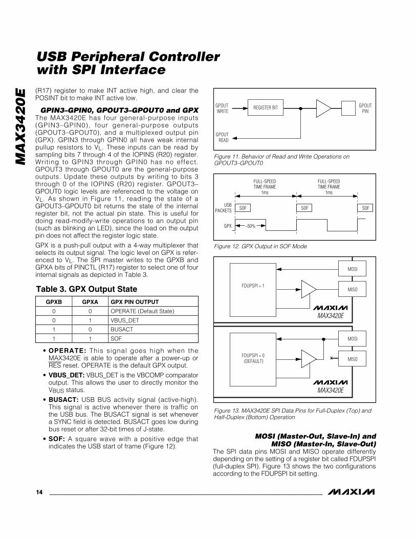
GPIN3–GPIN0, GPOUT3–GPOUT0 and GPXThe MAX3420E has four general-purpose inputs(GPIN3–GPIN0), four general-purpose outputs(GPOUT3–GPOUT0), and a multiplexed output pin(GPX). GPIN3 through GPIN0 all have weak internalpullup resistors to VL. These inputs can be read bysampling bits 7 through 4 of the IOPINS (R20) register.Writ ing to GPIN3 through GPIN0 has no effect.GPOUT3 through GPOUT0 are the general-purposeoutputs. Update these outputs by writing to bits 3through 0 of the IOPINS (R20) register. GPOUT3–GPOUT0 logic levels are referenced to the voltage onVL. As shown in Figure 11, reading the state of aGPOUT3–GPOUT0 bit returns the state of the internalregister bit, not the actual pin state. This is useful fordoing read-modify-write operations to an output pin(such as blinking an LED), since the load on the outputpin does not affect the register logic state.
GPX is a push-pull output with a 4-way multiplexer thatselects its output signal. The logic level on GPX is refer-enced to VL. The SPI master writes to the GPXB andGPXA bits of PINCTL (R17) register to select one of fourinternal signals as depicted in Table 3.
• OPERATE: This signal goes high when theMAX3420E is able to operate after a power-up orRES reset. OPERATE is the default GPX output.
• VBUS_DET: VBUS_DET is the VBCOMP comparatoroutput. This allows the user to directly monitor theVBUS status.
• BUSACT: USB BUS activity signal (active-high).This signal is active whenever there is traffic onthe USB bus. The BUSACT signal is set whenevera SYNC field is detected. BUSACT goes low duringbus reset or after 32-bit times of J-state.
• SOF: A square wave with a positive edge that indicates the USB start of frame (Figure 12).
MOSI (Master-Out, Slave-In) and MISO (Master-In, Slave-Out)
The SPI data pins MOSI and MISO operate differentlydepending on the setting of a register bit called FDUPSPI(full-duplex SPI). Figure 13 shows the two configurationsaccording to the FDUPSPI bit setting.
USB Peripheral Controllerwith SPI Interface
14 ______________________________________________________________________________________14 ______________________________________________________________________________________
REGISTER BITGPOUTWRITE
GPOUTREAD
GPOUTPIN
Figure 11. Behavior of Read and Write Operations onGPOUT3–GPOUT0
Table 3. GPX Output StateGPXB GPXA GPX PIN OUTPUT
0 0 OPERATE (Default State)
0 1 VBUS_DET
1 0 BUSACT
1 1 SOF
FULL-SPEEDTIME FRAME
1ms
FULL-SPEEDTIME FRAME
1ms
SOFUSB
PACKETS
GPX
SOF SOF
~50%
Figure 12. GPX Output in SOF Mode
FDUPSPI = 1
FDUPSPI = 0 (DEFAULT)
MAX3420E
MAX3420E
MOSI
MISO
MOSI
MISO
Figure 13. MAX3420E SPI Data Pins for Full-Duplex (Top) andHalf-Duplex (Bottom) Operation

In full-duplex mode (FDUPSPI=1), the MOSI and MISOpins are separate, and the MISO pin drives only when SSis low. In this mode, the first eight SCLK edges (after SS =0) clock the command byte into the MAX3420E on MOSI,and eight USB status bits are clocked out of theMAX3420E on MISO. For an SPI write cycle, any bytesfollowing the command byte are clocked into theMAX3420E on MOSI, and zeros are clocked out on MISO.For an SPI read cycle, any bytes following the commandbyte are clocked out of the MAX3420E on MISO and thedata on MOSI is ignored. At the conclusion of the SPIcycle (SS = 1), the MISO output tri-states.
In half-duplex mode, the MOSI pin is a bidirectional pinand the MISO pin is tri-stated. This saves a pin in the SPIinterface. Because of the shared data pin, this modedoes not offer the eight USB status bits (Figure 5) as thecommand byte is clocked into the MAX3420E. The MISOpin can be left unconnected in half-duplex mode.
SCLK (Serial Clock)The SPI master provides the MAX3420E SCLK signal toclock the SPI interface. SCLK has no low-frequency limit,and can be as high as 26MHz. The MAX3420E changesits output data (MISO) on the falling edge of SCLK andsamples input data (MOSI) on the rising edge of SCLK.The MAX3420E ignores SCLK transitions when SS ishigh. The inactive level of SCLK may be low or high,depending on the SPI operating mode (Figure 14).
SS (Slave Select)The MAX3420E SPI interface is active only when SS islow. When SS is high, the MAX3420E tri-states the SPIoutput pin and resets the internal MAX3420 SPI logic. If
SS goes high before a complete byte is clocked in, thebyte-in-progress is discarded. The SPI master can ter-minate an SPI cycle after clocking in the first 8 bits (thecommand byte). This feature can be used in a full-duplex system to retrieve the USB status bits (Figure 5)without sending or receiving SPI data. The MAX3420ESS pin is sensitive to undershoot. A 33pF capacitorshould be connected from the SS pin to ground to pre-vent any noise spikes.*
Application InformationSPI Interface
The MAX3420E operates as an SPI slave device. A reg-ister access consists of the SPI master first writing anSPI command byte, followed by reading or writing thecontents of the addressed register (see the RegisterDescription section for more detail). All SPI transfersare MSB (most significant bit) first. The external SPImaster provides a clock signal to the MAX3420E SCLKinput. This clock frequency can be between DC and26MHz. Bit transfers occur on the positive edge ofSCLK. The MAX3420E counts bits and divides theminto bytes. If fewer than 8 bits are clocked into theMAX3420E when SS goes high, the MAX3420E dis-cards the partial byte.
The MAX3420E SPI interface operates without adjust-ment in either SPI mode (CPOL = 0, CPHA = 0) or(CPOL = 1, CPHA = 1). No mode bit is required toselect between the two modes since the interface usesthe rising edge of the clock in both modes. The twoclocking modes are illustrated in Figure 14. Note thatthe inactive SCLK value is different for the two modes.Figure 14 illustrates the full-duplex mode, where data issimultaneously clocked into and out of the MAX3420E.
MA
X3
42
0E
USB Peripheral Controllerwith SPI Interface
______________________________________________________________________________________ 15
SS
MISO
MOSI
SCLKMODE 0,0
SCLKMODE 1,1
SPI MODE 0,0 OR 1,1
* MSB OF NEXT BYTE IN BURST MODE (SS REMAINS LOW)
Q7 Q6 Q5 Q4 Q3
D7 D6 D5 D4 D3 D2 D1 D0 *
Q2 Q1 Q0 *
Figure 14. SPI Clocking Modes
*33pF capacitor will not be required after redesign.

MA
X3
42
0E SPI Half- and Full-Duplex Operation
The MAX3420E can be programmed to operate in half-duplex (a bidirectional data pin) or full-duplex (onedata-in and one data-out pin) mode. The SPI mastersets a register bit called FDUPSPI (full-duplex SPI) to 1for full-duplex, and 0 for half-duplex operation. Half-duplex is the power-on default.
Full-Duplex OperationWhen the SPI master sets FDUPSPI = 1, the SPI inter-face uses separate data pins, MOSI and MISO to trans-fer data. Because of the separate data pins, bits canbe simultaneously clocked into and out of theMAX3420E. The MAX3420E makes use of this featureby clocking out 8 USB status bits as the command byteis clocked in, as illustrated in Figure 15.
Reading from the SPI Slave Interface (MISO)in Full-Duplex Mode
In full-duplex mode the SPI master reads data from theMAX3420E slave interface using the following steps:
(1) When SS is high, the MAX3420E is unselected andtri-states the MISO output.
(2) After driving SCLK to its inactive state, the SPI masterselects the MAX3420E by driving SS low. TheMAX3420E turns on its MISO output buffer and placesthe first data bit (Q7) on the MISO output (Figure 14).
(3) The SPI master simultaneously clocks the com-mand byte into the MAX3420E MOSI pin, and USBstatus bits out of the MAX3420E MISO pin on therising edges of the SCLK it supplies. TheMAX3420E changes its MISO output data on thefalling edges of SCLK.
(4) After eight clock cycles, the master can drive SShigh to deselect the MAX3420E, causing it to tri-state its MISO output. The falling edge of the clockputs the MSB of the next data byte in the sequenceon the MISO output (Figure 14).
(5) By keeping SS low, the master clocks register databytes out of the MAX3420E by continuing to supplySCLK pulses (burst mode). The master terminatesthe transfer by driving SS high. The master mustensure that SCLK is in its inactive state at thebeginning of the next access (when it drives SSlow). In full-duplex mode, the MAX3420E ignoresdata on MOSI while clocking data out on MISO.
Writing to the SPI Slave Interface (MOSI)in Full-Duplex Mode
In full-duplex mode, the SPI master writes data to theMAX3420E slave interface through the following steps:
(1) The SPI master sets the clock to its inactive state.While SS is high, the master can drive the MOSI pin.
(2) The SPI master selects the MAX3420E by drivingSS low and placing the first data bit to write on theMOSI input.
(3) The SPI master simultaneously clocks the com-mand byte into the MAX3420E and USB status bitsout of the MAX3420E MISO pin on the rising edgesof the SCLK it supplies. The SPI master changes itsMOSI input data on the falling edges of SCLK.
(4) After eight clock cycles, the master can drive SShigh to deselect the MAX3420E.
(5) By keeping SS low, the master clocks data bytesinto the MAX3420E by continuing to supply SCLKpulses (burst mode). The master terminates thetransfer by driving SS high. The master must ensurethat SCLK is inactive at the beginning of the nextaccess (when it drives SS low). In full-duplex mode,the MAX3420E outputs USB status bits on MISOduring the first 8 bits (the command byte), and sub-sequently outputs zeroes on MISO as the SPI mas-ter clocks bytes into MOSI.
Half-Duplex OperationThe MAX3420E is put into half-duplex mode at power-on, or when the SPI master clears the FDUPSPI bit. Inhalf-duplex mode, the MAX3420E tri-states its MISO pinand makes the MOSI pin bidirectional, saving a pin inthe SPI interface. The MISO pin can be left unconnect-ed in half-duplex operation.
Because of the single data pin, the USB status bitsavailable in full-duplex mode are not available as theSPI master clocks in the command byte. In half-duplexmode these status bits are accessed in the normal way,as register bits.
The SPI master must operate the MOSI pin as bidirec-tional. It accesses a MAX3420E register as follows:
(1) The SPI master sets the clock to its inactive state.While SS is high, the master can drive the MOSI pinto any value.
(2) The SPI master selects the MAX3420E by drivingSS low and placing the first data bit (MSB) to writeon the MOSI input.
(3) The SPI master turns on its output driver and clocksthe command byte into the MAX3420E on the risingedges of the SCLK it supplies. The SPI masterchanges its MOSI data on the falling edges of SCLK.
(4) After eight clock cycles, the master can drive SShigh to deselect the MAX3420E.
USB Peripheral Controllerwith SPI Interface
16 ______________________________________________________________________________________

(5) To write SPI data, the SPI master keeps its outputdriver on and clocks subsequent bytes into theMOSI pin. To read SPI data, after the eighth clockcycle the SPI master tri-states its output driver andbegins clocking in data bytes from the MOSI pin.
(6) The SPI master terminates the SPI cycle by return-ing SS high.
Figures 8 and 9 show timing diagrams for full- and half-duplex operation.
USB Serial-Interface EngineThe serial-interface engine (SIE) does most of thedetailed work required by USB protocol:
• USB packet PID detection and checking• CRC check and generation• Automatic retries in case of errors• USB packet generation• NRZI data encoding and decoding• Bit stuffing and unstuffing• Various USB error condition detection• USB bus reset, suspend, and wake-up detection• USB resume signaling• Automatic flow control (NAK)
PLLAn internal PLL multiplies the 12MHz oscillator signalby four to produce an internal 48MHz clock. When thechip is powered-down, the oscillator is turned off toconserve power. When re-powered, the oscillator andPLL require time to stabilize and lock. The OSCOKIRQinterrupt bit is used to indicate to the SPI master thatthe clocking system is stable and ready for operation.
Power ManagementAccording to USB rev. 2.0 specification, when a USBhost stops sending traffic for at least 3 milliseconds to aperipheral, the peripheral must enter a power-downstate called SUSPEND. Once suspended, the peripher-al must have enough of its internal logic active to rec-ognize when the host resumes signaling, or if enabledfor remote wakeup, that the SPI master wishes to signala resume event. The following sections titled Suspendand Wakeup and USB Resume describe how the SPImaster coordinates with the MAX3420E to accomplishthis power management.
SuspendAfter three milliseconds of USB bus inactivity, a USBperipheral is required to enter the USB suspend stateand draw no more than 500µA of supply current. Toaccomplish this, after three milliseconds of USB businactivity, the MAX3420E sets the SUSPIRQ bit in theUSBIRQ (R13) register and asserts the INT output, ifSUSPIE = 1 and IE = 1. The SPI master must do anynecessary power-saving housekeeping and then setthe PWRDOWN bit in the USBCTL (R15) register. Thisinstructs the MAX3420E to enter a power-down state, inwhich it does the following:
• Stops the 12MHz oscillator
• Keeps the INT output active (according to the mode set in the PINCTL (R17) register)
• Monitors the USB D+ line for bus activity
• Monitors the SPI port for any traffic
Note that the MAX3420E does not automatically entera power-down state after three milliseconds of businactivity. This allows the SPI master to perform any
MA
X3
42
0E
USB Peripheral Controllerwith SPI Interface
______________________________________________________________________________________ 17
SS
MISO
MOSI
SCLK
SPI MODE 0,0 (CPOL = 0, CPHA = 0)
SUSPIRQ URESIRQ SUDAVIRQ IN3BAVIRQ IN2BAVIRQ
REG 4 REG 3 REG 2 REG 1 REG 0 0 DIR ACKSTAT
OUT1DAVIRQ OUT0DAVIRQ IN0BAVIRQ X
Figure 15. SPI Port in Full-Duplex Mode

MA
X3
42
0E pre-shutdown tasks before it requests the MAX3420E to
enter the power-down state by setting PWRDOWN = 1.
Wakeup and USB ResumeThe MAX3420E may wake up in three ways while it is inthe power-down state:(1) The SPI master clears the PWRDOWN bit in the
USBCTL (R15) register (this is also achieved by achip reset).
(2) The SPI master signals a USB remote wakeup bysetting the SIGRWU bit in the USBCTL (R15) regis-ter. When SIGRWU = 1, the MAX3420E restarts theoscillator and waits for it to stabilize. After the oscil-lator stabilizes, the MAX3420E drives RESUME sig-naling (a 10ms K-state) on the bus. The MAX3420Etimes this interval to relieve the SPI master of havingto keep accurate time. The MAX3420E also ensuresthat the RESUME signal begins only after at least5ms of the bus idle state. When the MAX3420E fin-ishes its RESUME signaling, it sets the RWUDNIRQ(remote-wakeup-done interrupt request) interruptflag in the USBIRQ (R13) register. At this time theSPI master should clear the SIGRWU bit.
(3) The host resumes bus activity. To enable theMAX3420E to wake up from host signaling, the SPImaster sets the HOSCSTEN (host oscillator startenable) bit of the USBCTL (R15) register. While inthis mode, if the MAX3420E detects a 1 to 0 transi-tion on D+, the MAX3420E restarts the oscillatorand waits for it to stabilize.
Device ResetThe MAX3420E has three reset mechanisms:
• Power-On Reset. This is the most inclusive reset (sets all internal register bits to a known state).
• Chip Reset. The SPI master can assert a chipreset by setting the bit CHIPRES = 1, which hasthe same effect as pulling the RES pin low. Thisreset clears only some register bits and leaves others alone.
• USB Bus Reset. A USB bus reset is the leastinclusive (clears the smallest number of bits).
Power-On ResetAt power-on, all register bits except three are cleared.The following three bits are set to 1 to indicate that theIN FIFOs are available for loading by the SPI master(BAV = buffer available):
• IN3BAVIRQ• IN2BAVIRQ• IN0BAVIRQ
Chip ResetPulling the RES pin low or setting CHIPRES = 1 clearsmost of the bits that control USB operation, but keepsthe SPI and pin-control bits unchanged so the interfacebetween the SPI master and the MAX3420E is not dis-turbed. Specifically:
• CHIPRES is unchanged. If the SPI master assertedthis reset by setting CHIPRES = 1, it removes thereset by writing CHIPRES = 0.
• CONNECT is unchanged, keeping the device connected if CONNECT = 1.
• The general-purpose outputs GPOUT3–GPOUT0are unchanged, preventing output glitches.
• The GPX output selector (GPXB, GPXA) isunchanged.
• The bits that control the SPI interface areunchanged: FDUPSPI, INTLEVEL, and POSINT.
• The bits that control power-down and wakeupbehavior are unchanged: HOSCSTEN, PWRDOWN,and SIGRWU.
All other bits except the three noted in the Power-OnReset section are cleared.
Note: The IRQ and IE bits are cleared using this reset.This means that firmware routines that enable interruptsshould be called after a reset of this type.
USB Bus ResetWhen the MAX3420E detects 21.33µs of SE0, it assertsthe URESIRQ bit and clears certain bits. This reset isthe least inclusive of the three resets. It maintains thebit states listed in the Power-On Reset and Chip Resetsections, plus it leaves the following bits in their previ-ous states:
• Registers R0-R4 are unchanged. The actual data in the FIFOs is never cleared.
• The IE bit is unchanged.
• URESIE, URESIRQ, URESDNIE, and URESDNIRQare unchanged, allowing the SPI master to check the state of USB bus resets.
As with the chip reset, most of the interrupt request andinterrupt enable bits are cleared, meaning that thedevice firmware must reenable individual interrupts aftera bus reset. The exceptions are the interrupts associat-ed with the actual bus reset, allowing the SPI master todetect the beginning and end of the host signaling USB bus reset.
USB Peripheral Controllerwith SPI Interface
18 ______________________________________________________________________________________
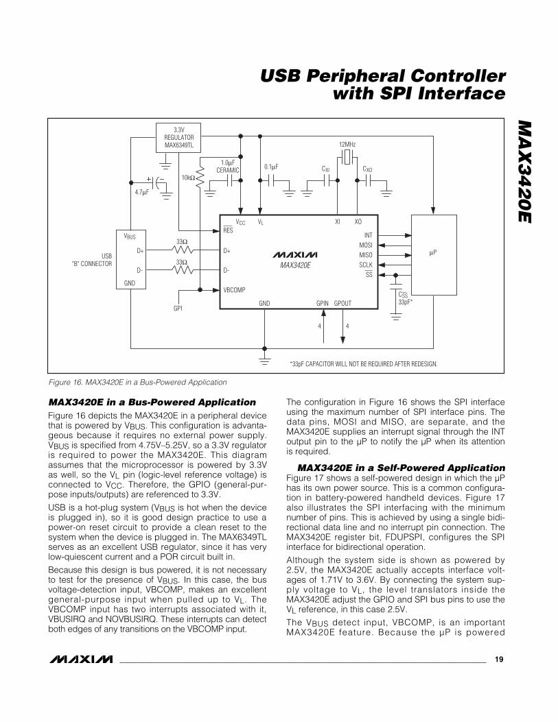
MAX3420E in a Bus-Powered ApplicationFigure 16 depicts the MAX3420E in a peripheral devicethat is powered by VBUS. This configuration is advanta-geous because it requires no external power supply.VBUS is specified from 4.75V–5.25V, so a 3.3V regulatoris required to power the MAX3420E. This diagramassumes that the microprocessor is powered by 3.3Vas well, so the VL pin (logic-level reference voltage) isconnected to VCC. Therefore, the GPIO (general-pur-pose inputs/outputs) are referenced to 3.3V.
USB is a hot-plug system (VBUS is hot when the deviceis plugged in), so it is good design practice to use apower-on reset circuit to provide a clean reset to thesystem when the device is plugged in. The MAX6349TLserves as an excellent USB regulator, since it has verylow-quiescent current and a POR circuit built in.
Because this design is bus powered, it is not necessaryto test for the presence of VBUS. In this case, the busvoltage-detection input, VBCOMP, makes an excellentgeneral-purpose input when pulled up to VL. TheVBCOMP input has two interrupts associated with it,VBUSIRQ and NOVBUSIRQ. These interrupts can detectboth edges of any transitions on the VBCOMP input.
The configuration in Figure 16 shows the SPI interfaceusing the maximum number of SPI interface pins. Thedata pins, MOSI and MISO, are separate, and theMAX3420E supplies an interrupt signal through the INToutput pin to the µP to notify the µP when its attentionis required.
MAX3420E in a Self-Powered ApplicationFigure 17 shows a self-powered design in which the µPhas its own power source. This is a common configura-tion in battery-powered handheld devices. Figure 17also illustrates the SPI interfacing with the minimumnumber of pins. This is achieved by using a single bidi-rectional data line and no interrupt pin connection. TheMAX3420E register bit, FDUPSPI, configures the SPIinterface for bidirectional operation.
Although the system side is shown as powered by2.5V, the MAX3420E actually accepts interface volt-ages of 1.71V to 3.6V. By connecting the system sup-ply voltage to VL, the level translators inside theMAX3420E adjust the GPIO and SPI bus pins to use theVL reference, in this case 2.5V.
The VBUS detect input, VBCOMP, is an importantMAX3420E feature. Because the µP is powered
MA
X3
42
0E
USB Peripheral Controllerwith SPI Interface
______________________________________________________________________________________ 19
MAX3420E
VCC VL XI XO
INTMOSIMISOSCLK
RES
D+
D-
D+
D-
VBCOMP
SS
0.1µF
10kΩ
GPI
GND
VBUS33Ω
33Ω
1.0µFCERAMIC CXI CXO
12MHz
3.3VREGULATORMAX6349TL
µP
44
USB"B" CONNECTOR
CSS33pF*GND GPIN GPOUT
4.7µF
Figure 16. MAX3420E in a Bus-Powered Application
*33pF CAPACITOR WILL NOT BE REQUIRED AFTER REDESIGN.

MA
X3
42
0E
whether the USB device is plugged in or not, it needssome way to detect a plug-in event. A comparatorinside the MAX3420E checks for a valid VBUS connec-tion on VBCOMP and provides a connect status bit tothe µP. Once connected, the µP can delay the logicalconnection to the USB bus to perform any required ini-tialization, and then connect by setting the CONNECTbit to 1 in the MAX3420E register USBCTL (R15). Thisconnects the internal 1.5kΩ resistor from D+ to VCC, tosignal the host that a device has been plugged in.
If a host turns off VBUS while the device is connected,the USB rev. 2.0 specification requires that the devicemust not power its 1.5kΩ pullup resistor connected toD+. The MAX3420E has two features to help servicethis event. First, the NOVBUSIRQ bit indicates the lossof VBUS. Second, the µP can set a bit called VBGATE(VBUS gate) to instruct the MAX3420E to disconnect thepullup resistor anytime VBUS goes away, regardless ofthe CONNECT bit setting.
Crystal SelectionThe MAX3420E requires a crystal with the followingspecifications:
Frequency: 12MHz ± 0.25%
CLOAD: 18pF
CO: 7pf max
Drive level: 200µW
Series resonance resistance: 60Ω max
Note: Series resonance resistance is the resistanceobserved when the resonator is in the series resonantcondition. This is a parameter often stated by quartz crys-tal vendors and is called R1. When a resonator is used inthe parallel resonant mode with an external load capaci-tance, as is the case with the MAX3420E oscillator circuit,the effective resistance is sometimes stated. This effec-tive resistance at the loaded frequency of oscillation is:
R1 x ( 1 + (CO / CLOAD))2
For typical CO and CLOAD values, the effective resis-tance can be greater than R1 by a factor of 2.
ESD ProtectionD+, D-, and VBCOMP possess extra protection againststatic electricity to protect the devices up to ±15kV. TheESD structures withstand high ESD in all operatingmodes: normal operation, suspend mode, and pow-ered down. VBCOMP and VCC require 1µF ceramic
USB Peripheral Controllerwith SPI Interface
20 ______________________________________________________________________________________
MAX3420E
VCC VL XI XO
N.C.
N.C.
INTMOSIMISOSCLK
RES
D+
D-
D+
D-
VBCOMP
SS
0.1µF
GND
GND GPIN GPOUT
VBUS33Ω
33Ω
1.0µFCERAMIC
1.0µFCERAMIC
CXI CXO
12MHz
3.3VREGULATORMAX6349TL
µP
44
USB "B" CONNECTOR
CSS33pF*
+2.5V
4.7µF
Figure 17. MAX3420E in a Self-Powered Application
*33pF CAPACITOR WILL NOT BE REQUIRED AFTER REDESIGN.

capacitors connected to ground as close to the pins aspossible. D+, D-, and VBCOMP provide protection tothe following limits:
• ±15kV using the Human Body Model
• ±8kV using the Contact Discharge method specifiedin IEC 61000-4-2
• ±12kV using the IEC 61000-4-2 Air Gap Method
ESD Test ConditionsESD performance depends on a variety of conditions.Contact Maxim for a reliability report that documentstest setup, test methodology, and test results.
Human Body ModelFigure 18 shows the Human Body Model, and Figure 19shows the current waveform generated when dis-charged into a low impedance. This model consists ofa 100pF capacitor charged to the ESD voltage of inter-est, which then discharges into the test device througha 1.5kΩ resistor.
IEC 61000-4-2The IEC 61000-4-2 standard covers ESD testing andperformance of finished equipment. It does not specifi-cally refer to integrated circuits. The major differencebetween tests done using the Human Body Model andIEC 61000-4-2 is a higher peak current in IEC 61000-4-2, due to lower series resistance. Hence, the ESD with-stand voltage measured to IEC 61000-4-2 generally islower than that measured using the Human BodyModel. Figure 20 shows the IEC 61000-4-2 model. TheContact Discharge method connects the probe to thedevice before the probe is charged. The Air-GapDischarge test involves approaching the device with acharged probe.
Short-Circuit ProtectionThe MAX3420E withstands VBUS shorts to D+ and D-on the USB connector side of the 33Ω series resistors.
Chip InformationPROCESS: BiCMOS
MA
X3
42
0E
USB Peripheral Controllerwith SPI Interface
______________________________________________________________________________________ 21
Figure 19. Human Body Model Current Waveform
IP 100%90%
36.8%
tRLTIME
tDLCURRENT WAVEFORM
PEAK-TO-PEAK RINGING(NOT DRAWN TO SCALE)
Ir
10%0
0
AMPERES
Figure 18. Human Body ESD Test Models
CHARGE-CURRENT-LIMIT RESISTOR
DISCHARGERESISTANCE
STORAGECAPACITOR
Cs100pF
RC1MΩ
RD1.5kΩ
HIGH-VOLTAGE
DCSOURCE
DEVICEUNDERTEST
Figure 20. IEC 61000-4-2 ESD Test Model
CHARGE-CURRENT-LIMIT RESISTOR
DISCHARGERESISTANCE
STORAGECAPACITOR
Cs150pF
RC50MΩ to 100MΩ
RD100MΩ
HIGH- VOLTAGE
DCSOURCE
DEVICEUNDERTEST

MA
X3
42
0E
USB Peripheral Controllerwith SPI Interface
22 ______________________________________________________________________________________
Package Information(The package drawing(s) in this data sheet may not reflect the most current specifications. For the latest package outline informationgo to www.maxim-ic.com/packages.)
24L
QFN
TH
IN.E
PS
PACKAGE OUTLINE,
21-0139 21
D
12, 16, 20, 24, 28L THIN QFN, 4x4x0.8mm
PACKAGE OUTLINE,
21-0139 22
D
12, 16, 20, 24, 28L THIN QFN, 4x4x0.8mm
MA
X3
42
0E
USB Peripheral Controllerwith SPI Interface
Maxim cannot assume responsibility for use of any circuitry other than circuitry entirely embodied in a Maxim product. No circuit patent licenses areimplied. Maxim reserves the right to change the circuitry and specifications without notice at any time.
Maxim Integrated Products, 120 San Gabriel Drive, Sunnyvale, CA 94086 408-737-7600 ____________________ 23
© 2005 Maxim Integrated Products Printed USA is a registered trademark of Maxim Integrated Products, Inc.
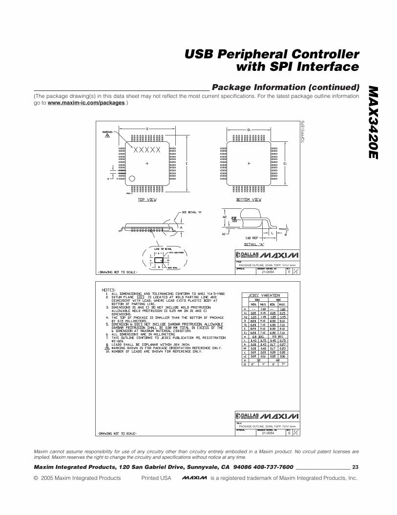
Package Information (continued)(The package drawing(s) in this data sheet may not reflect the most current specifications. For the latest package outline informationgo to www.maxim-ic.com/packages.)
TQFP
PO
.EP
S
E1
221-0054
PACKAGE OUTLINE, 32/48L TQFP, 7x7x1.4mm
E2
221-0054
PACKAGE OUTLINE, 32/48L TQFP, 7x7x1.4mm