USB 3.0 Board - Altera · 3.0 high-speed device and host control interface. The board is enriched...
53
System Level Solutions, Inc. (USA) 14100 Murphy Avenue San Martin, CA 95046 (408) 852 - 0067 http://www.slscorp.com Board Version: r2c Document Version: 1.5 Document Date: April 2016 USB 3.0 Development Board Reference Manual
Transcript of USB 3.0 Board - Altera · 3.0 high-speed device and host control interface. The board is enriched...
System Level Solutions, Inc. (USA) 14100 Murphy AvenueSan Martin, CA 95046 (408) 852 - 0067
http://www.slscorp.com
Board Version: r2c
Document Version: 1.5 Document Date: April 2016
USB 3.0 Development BoardReference Manual
ii System Level SolutionsApril 2016USB 3.0 Development Board Reference Manual
Copyright ©2011-2016, System Level Solutions, Inc. (SLS) All rights reserved. SLS, an Embedded systems company, the stylized SLS logo, specific device designations, and all other words and logos that are identified as trademarks and/or service marks are, unless noted otherwise, the trademarks and service marks of SLS in India and other countries. All other products or service names are the property of their respective holders. SLS products are protected under numerous U.S. and foreign patents and pending applications, mask working rights, and copyrights. SLS reserves the right to make changes to any products and services at any time without notice. SLS assumes no responsibility or liability arising out of the application or use of any information, products, or service described herein except as expressly agreed to in writing by SLS. SLS customers are advised to obtain the latest version of specifications before relying on any published information and before orders for products or services.
rm_dbusb30_1.5
About this Manual
Introduction This manual provides component details of the USB 3.0 development board.
Table below shows the revision history of the manual.
How to find Information
• The Adobe Acrobat Find feature allows you to search the contents of a PDF file. Use Ctrl + F to open the Find dialog box. Use Shift + Ctrl + N to open to the Go To Page dialog box.
• Bookmarks serve as an additional table of contents.
• Thumbnail icons, which provide miniature preview of each page, provide a link to the pages.
• Numerous links shown in Navy Blue color allow you to jump to related information.
Version Date Description
1.5 April 2016 • Updated description of DDR2 SDRAM (U3)
1.4 December 2011 • Removed 3.row in table 2.26
1.3 October 2011 • Updated Figure 1.1 and Figure 2.1
1.2 August 2011 • Update the reference manual as per the new release of the board version r2c
• Added board and device references in all table
1.1 May 2011 • Modified text in all chapter
• Added chapter 3 in power supply section of chapter 2
• Removed chapter 3
• Updated Figure 1-1. with SMA Connector
1.0 March 2011 • First Publication of the Reference Manual
iii
USB 3.0 Development Board Reference ManualSystem Level SolutionsApril 2016
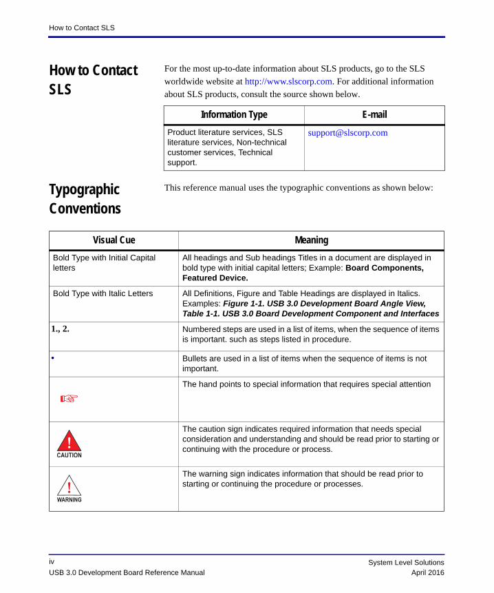
How to Contact SLS
How to Contact SLS
For the most up-to-date information about SLS products, go to the SLS
worldwide website at http://www.slscorp.com. For additional information
about SLS products, consult the source shown below.
Typographic Conventions
This reference manual uses the typographic conventions as shown below:
Information Type E-mail
Product literature services, SLS literature services, Non-technical customer services, Technical support.
Visual Cue Meaning
Bold Type with Initial Capital letters
All headings and Sub headings Titles in a document are displayed in bold type with initial capital letters; Example: Board Components, Featured Device.
Bold Type with Italic Letters All Definitions, Figure and Table Headings are displayed in Italics. Examples: Figure 1-1. USB 3.0 Development Board Angle View, Table 1-1. USB 3.0 Board Development Component and Interfaces
1., 2. Numbered steps are used in a list of items, when the sequence of items is important. such as steps listed in procedure.
• Bullets are used in a list of items when the sequence of items is not important.
The hand points to special information that requires special attention
The caution sign indicates required information that needs special consideration and understanding and should be read prior to starting or continuing with the procedure or process.
The warning sign indicates information that should be read prior to starting or continuing the procedure or processes.
iv System Level SolutionsApril 2016USB 3.0 Development Board Reference Manual
v
USB 3.0 Development Board Reference Manual
System Level SolutionsApril 2016
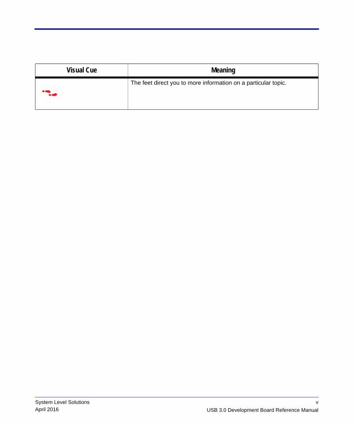
Visual Cue Meaning
The feet direct you to more information on a particular topic.
Content
About this Manual.............................................................................................................. iiiIntroduction..............................................................................................................................................iii
How to find Information ..........................................................................................................................iii
How to Contact SLS ................................................................................................................................ iv
Typographic Conventions ........................................................................................................................ iv
1. Introduction ............................................................................................................................... 1General Description .................................................................................................................................. 1
Features ..................................................................................................................................................... 1
Component Blocks............................................................................................................................. 2
Block Diagram................................................................................................................................... 4
Handling the Board ............................................................................................................................ 4
2. Board Component..................................................................................................................... 5Featured Device ........................................................................................................................................ 7
Cyclone IV E Device (U1)................................................................................................................. 7
Configuration Circuitry............................................................................................................................. 9
Configuring the Cyclone IV E FPGA................................................................................................ 9
JTAG Programming........................................................................................................................... 9
JTAG Header (J1) .............................................................................................................................. 9
Serial Configuration Device - EPCS64 (U2) ................................................................................... 10
Memory Device....................................................................................................................................... 11
DDR2 SDRAM (U3) ....................................................................................................................... 11
NAND Flash (U9-U13) ................................................................................................................... 13
SDR SDRAM (U17) ........................................................................................................................ 15
CFI Flash (U18) ............................................................................................................................... 17
General User Input and Output ............................................................................................................... 19
LEDs ................................................................................................................................................ 19
Reset Switch (SW1)......................................................................................................................... 21
Push-button Switches (SW2-SW5).................................................................................................. 21
viSystem Level Solutions
DIP Switches (SW7)........................................................................................................................ 22
USB 3.0 Connector (CON1) ............................................................................................................ 22
USB 3.0 PHY (U14) ........................................................................................................................ 23
Mini USB Connector (CON3) ......................................................................................................... 27
USB UART (U16) ........................................................................................................................... 27
Micro SD Card Connector (CON6) ................................................................................................. 28
Expansion Interface................................................................................................................................. 29
HSMC Connector (J3) ..................................................................................................................... 29
General Purpose I/O Headers (J6, J7).............................................................................................. 33
Clock Circuitry........................................................................................................................................ 34
Crystal Oscillator (Y1)..................................................................................................................... 34
SMA RA Connectors (CON4 & CON5) ......................................................................................... 35
Power Supply .......................................................................................................................................... 35
Power Switch (SW6) ....................................................................................................................... 37
HSMC Power Supply Select Header (J1) ........................................................................................ 37
Power Connector (J2, J3)................................................................................................................. 38
Power Header (J4, J5) ...................................................................................................................... 42
vii
USB 3.0 Development Board Reference Manual
System Level SolutionsApril 2016
1. Introduction
General Description
The USB 3.0 development board provides a hardware platform for developing and prototyping low-power, high-volume, feature-rich designs as
well as to demonstrate the on-board USB 3.0 interface. The board contains
Altera’s low power and low cost Cyclone IV E FPGA EP4CE75F29C7N with
transceiver variants. The board uses TUSB1310AZAY PHY Chip for USB
3.0 high-speed device and host control interface. The board is enriched with
the high-speed memory components which includes DDR2 SDRAM, NAND
Flash, CFI Flash and SDRAM. The board contains Micro SD card connector
as external memory storage media.
USB 3.0 development board is powered with the power add on board which
is plugged on the base board connector, to supply the power to each
component of the board. The board functionality can be expanded through
Altera High Speed Mezzanine Card (HSMC) connector. SLS and other Altera
development kit partners have made the daughter cards which allow you to
expand the functionality of the board. The board also has the user interface
like LEDs and push-button switches.
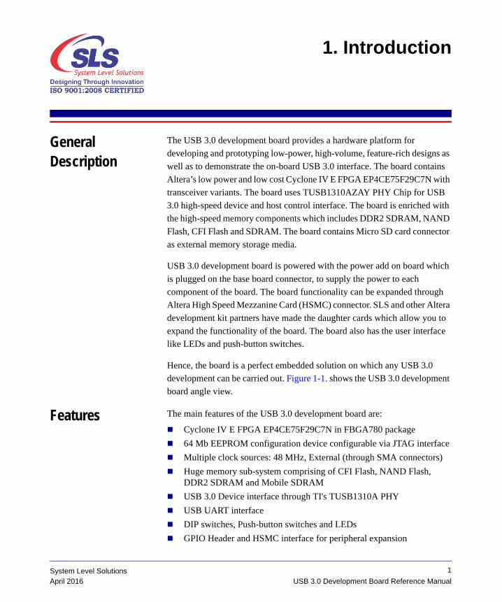
Hence, the board is a perfect embedded solution on which any USB 3.0
development can be carried out. Figure 1-1. shows the USB 3.0 development
board angle view.
Features The main features of the USB 3.0 development board are:
Cyclone IV E FPGA EP4CE75F29C7N in FBGA780 package
64 Mb EEPROM configuration device configurable via JTAG interface
Multiple clock sources: 48 MHz, External (through SMA connectors)
Huge memory sub-system comprising of CFI Flash, NAND Flash, DDR2 SDRAM and Mobile SDRAM
USB 3.0 Device interface through TI's TUSB1310A PHY
USB UART interface
DIP switches, Push-button switches and LEDs
GPIO Header and HSMC interface for peripheral expansion
1
USB 3.0 Development Board Reference ManualSystem Level SolutionsApril 2016
Features
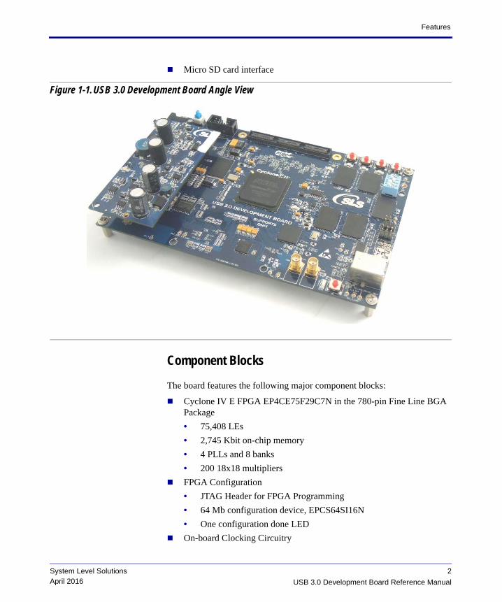
Micro SD card interface
Figure 1-1. USB 3.0 Development Board Angle View
Component Blocks
The board features the following major component blocks:
Cyclone IV E FPGA EP4CE75F29C7N in the 780-pin Fine Line BGA Package
• 75,408 LEs
• 2,745 Kbit on-chip memory
• 4 PLLs and 8 banks
• 200 18x18 multipliers
FPGA Configuration
• JTAG Header for FPGA Programming
• 64 Mb configuration device, EPCS64SI16N
• One configuration done LED
On-board Clocking Circuitry
2
USB 3.0 Development Board Reference Manual
System Level SolutionsApril 2016
Features
• 48-MHz oscillator
• SMA connectors for external clock input
• SMA connectors for external clock output
Memory Devices
• 64 Mb CFI Flash with 16-bit data bus
• 1 Gb DDR2 SDRAM with 16-bit data bus
• 64 Mb Mobile SDRAM with 16-bit data bus
Optional Memory Devices
• Five NAND Flash devices with shared data and control bus
USB 3.0 Interface
• 5.0 Gbps USB 3.0 Transceiver, TUSB1310AZAY
USB UART Interface
• USB to Serial UART Interface, FT232R
Peripheral Expansion & GPIO
• High Speed Mezzanine Card (HSMC) interface
• Two GPIO headers (3x2 header)
• 4x2 GPIO header
LEDs
• Four user LEDs
• Power LED
• Reset LED
Switches
• Four user DIP switches
• Four user push-button switches
• Reset push-button switch
• Power ON/OFF switch
Power
• 15V@3A DC input
Mechanical
• PCB size is 7.0" X 4.5"
3 System Level SolutionsApril 2016USB 3.0 Development Board Reference Manual
Features
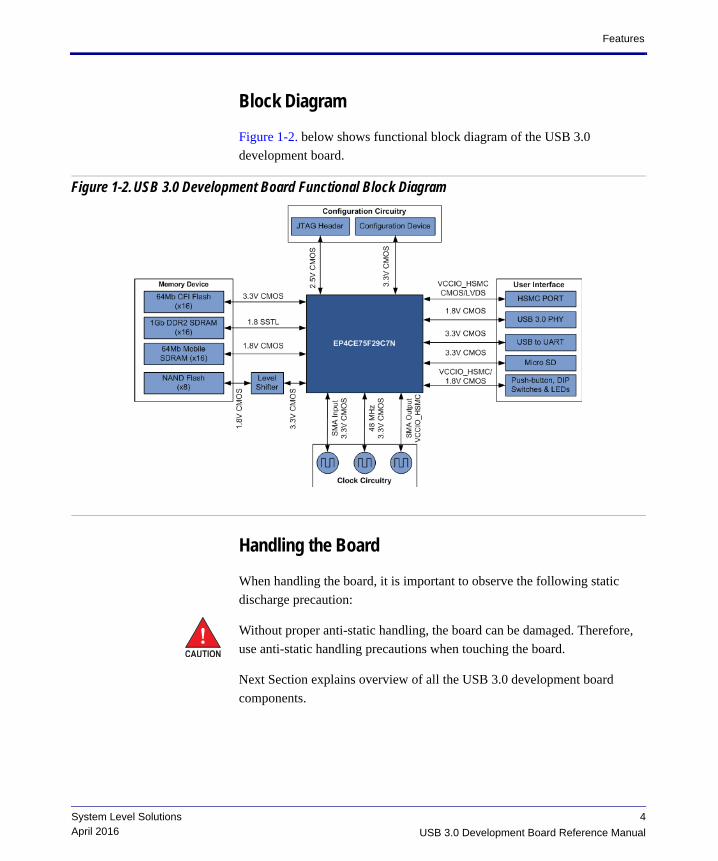
Block Diagram
Figure 1-2. below shows functional block diagram of the USB 3.0
development board.
Figure 1-2. USB 3.0 Development Board Functional Block Diagram
Handling the Board
When handling the board, it is important to observe the following static
discharge precaution:
Without proper anti-static handling, the board can be damaged. Therefore,
use anti-static handling precautions when touching the board.
Next Section explains overview of all the USB 3.0 development board
components.
4
USB 3.0 Development Board Reference Manual
System Level SolutionsApril 2016
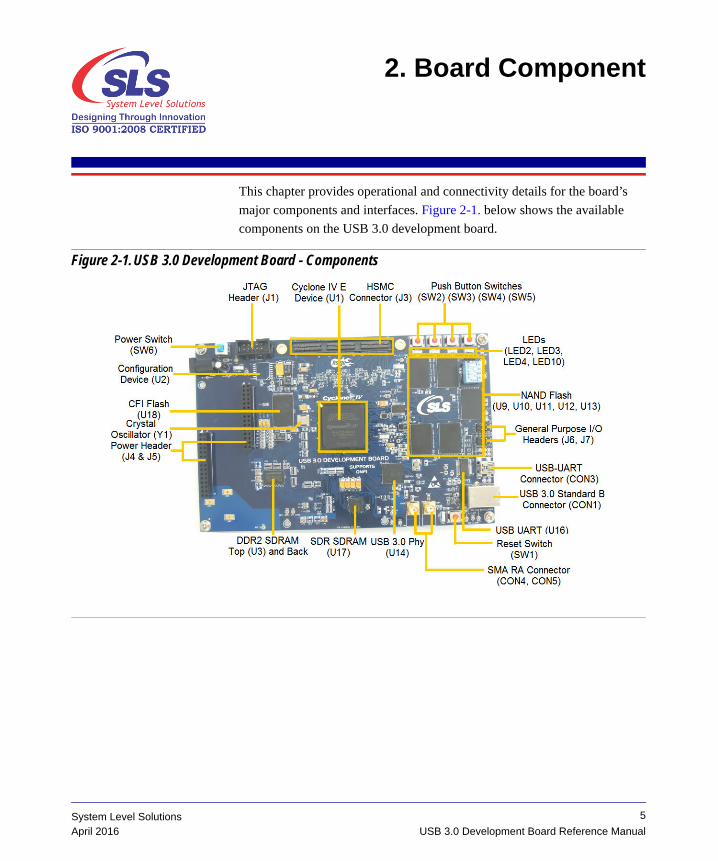
2. Board Component
This chapter provides operational and connectivity details for the board’s
major components and interfaces. Figure 2-1. below shows the available
components on the USB 3.0 development board.
Figure 2-1. USB 3.0 Development Board - Components
5
USB 3.0 Development Board Reference ManualSystem Level SolutionsApril 2016
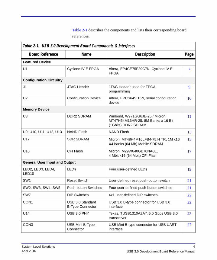
Table 2-1 describes the components and lists their corresponding board
references.
Table 2-1. USB 3.0 Development Board Components & Interfaces
Board Reference Name Description Page
Featured Device
U1 Cyclone IV E FPGA Altera, EP4CE75F29C7N, Cyclone IV E FPGA
7
Configuration Circuitry
J1 JTAG Header JTAG Header used for FPGA programming
9
U2 Configuration Device Altera, EPCS64SI16N, serial configuration device
10
Memory Device
U3 DDR2 SDRAM Winbond, W971GG6JB-25 / Micron, MT47H64M16HR-25, 8M Banks x 16 Bit (1Gbits) DDR2 SDRAM
11
U9, U10, U11, U12, U13 NAND Flash NAND Flash 13
U17 SDR SDRAM Micron, MT48H4M16LFB4-75:H TR, 1M x16 X4 banks (64 Mb) Mobile SDRAM
15
U18 CFI Flash Micron, M29W640GB70NA6E, 4 Mbit x16 (64 Mbit) CFI Flash
17
General User Input and Output
LED2, LED3, LED4, LED10
LEDs Four user-defined LEDs 19
SW1 Reset Switch User-defined reset push-button switch 21
SW2, SW3, SW4, SW5 Push-button Switches Four user-defined push-button switches 21
SW7 DIP Switches 4x1 user-defined DIP switches 22
CON1 USB 3.0 Standard B-Type Connector
USB 3.0 B-type connector for USB 3.0 interface
22
U14 USB 3.0 PHY Texas, TUSB1310AZAY, 5.0 Gbps USB 3.0 transceiver
23
CON3 USB Mini B-Type Connector
USB Mini B-type connector for USB UART interface
27
6
USB 3.0 Development Board Reference Manual
System Level SolutionsApril 2016
Featured Device
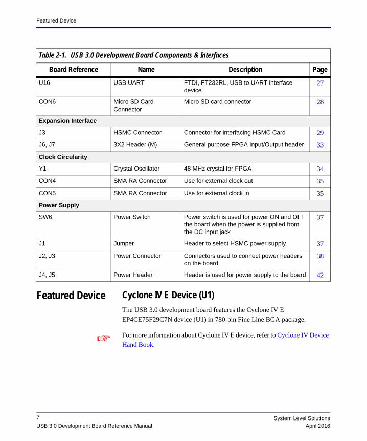
Featured Device Cyclone IV E Device (U1)
The USB 3.0 development board features the Cyclone IV E
EP4CE75F29C7N device (U1) in 780-pin Fine Line BGA package.
For more information about Cyclone IV E device, refer to Cyclone IV Device
Hand Book.
U16 USB UART FTDI, FT232RL, USB to UART interface device
27
CON6 Micro SD Card Connector
Micro SD card connector 28
Expansion Interface
J3 HSMC Connector Connector for interfacing HSMC Card 29
J6, J7 3X2 Header (M) General purpose FPGA Input/Output header 33
Clock Circularity
Y1 Crystal Oscillator 48 MHz crystal for FPGA 34
CON4 SMA RA Connector Use for external clock out 35
CON5 SMA RA Connector Use for external clock in 35
Power Supply
SW6 Power Switch Power switch is used for power ON and OFF the board when the power is supplied from the DC input jack
37
J1 Jumper Header to select HSMC power supply 37
J2, J3 Power Connector Connectors used to connect power headers on the board
38
J4, J5 Power Header Header is used for power supply to the board 42
Table 2-1. USB 3.0 Development Board Components & Interfaces
Board Reference Name Description Page
7 System Level SolutionsApril 2016USB 3.0 Development Board Reference Manual
Featured Device
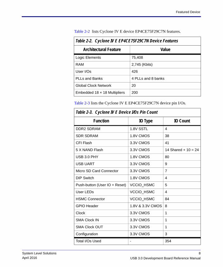
Table 2-2 lists Cyclone IV E device EP4CE75F29C7N features.
Table 2-3 lists the Cyclone IV E EP4CE75F29C7N device pin I/Os.
Table 2-2. Cyclone IV E EP4CE75F29C7N Device Features
Architectural Feature Value
Logic Elements 75,408
RAM 2,745 (Kbits)
User I/Os 426
PLLs and Banks 4 PLLs and 8 banks
Global Clock Network 20
Embedded 18 × 18 Multipliers 200
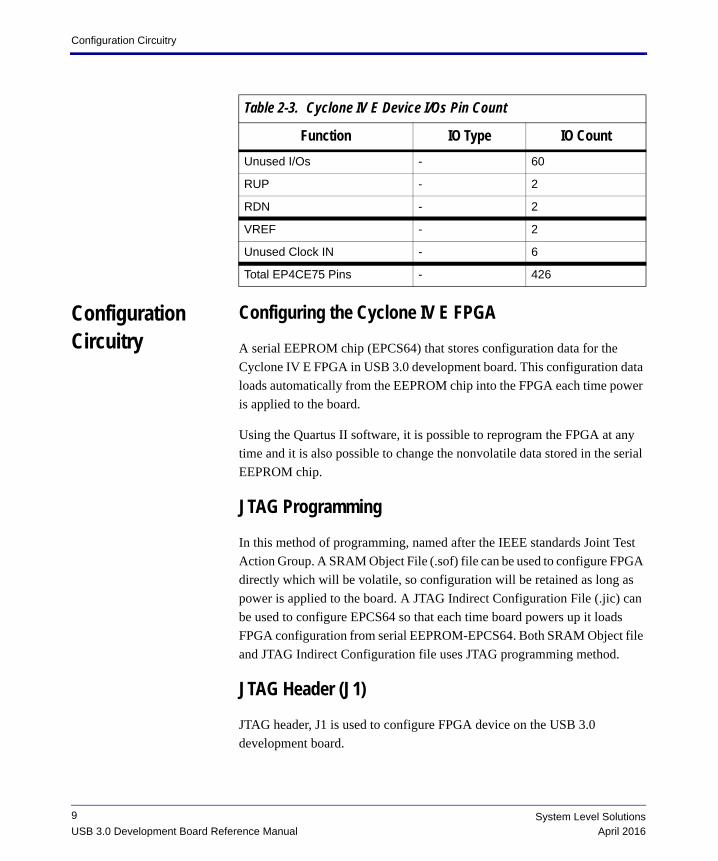
Table 2-3. Cyclone IV E Device I/Os Pin Count
Function IO Type IO Count
DDR2 SDRAM 1.8V SSTL 4
SDR SDRAM 1.8V CMOS 38
CFI Flash 3.3V CMOS 41
5 X NAND Flash 3.3V CMOS 14 Shared + 10 = 24
USB 3.0 PHY 1.8V CMOS 80
USB UART 3.3V CMOS 9
Micro SD Card Connector 3.3V CMOS 7
DIP Switch 1.8V CMOS 4
Push-button (User IO + Reset) VCCIO_HSMC 5
User LEDs VCCIO_HSMC 4
HSMC Connector VCCIO_HSMC 84
GPIO Header 1.8V & 3.3V CMOS 8
Clock 3.3V CMOS 1
SMA Clock IN 3.3V CMOS 1
SMA Clock OUT 3.3V CMOS 1
Configuration 3.3V CMOS 3
Total I/Os Used - 354
8
USB 3.0 Development Board Reference Manual
System Level SolutionsApril 2016
Configuration Circuitry
Configuration Circuitry
Configuring the Cyclone IV E FPGA
A serial EEPROM chip (EPCS64) that stores configuration data for the
Cyclone IV E FPGA in USB 3.0 development board. This configuration data
loads automatically from the EEPROM chip into the FPGA each time power
is applied to the board.
Using the Quartus II software, it is possible to reprogram the FPGA at any
time and it is also possible to change the nonvolatile data stored in the serial
EEPROM chip.
JTAG Programming
In this method of programming, named after the IEEE standards Joint Test Action Group. A SRAM Object File (.sof) file can be used to configure FPGA
directly which will be volatile, so configuration will be retained as long as
power is applied to the board. A JTAG Indirect Configuration File (.jic) can
be used to configure EPCS64 so that each time board powers up it loads
FPGA configuration from serial EEPROM-EPCS64. Both SRAM Object file
and JTAG Indirect Configuration file uses JTAG programming method.
JTAG Header (J1)
JTAG header, J1 is used to configure FPGA device on the USB 3.0
development board.
Unused I/Os - 60
RUP - 2
RDN - 2
VREF - 2
Unused Clock IN - 6
Total EP4CE75 Pins - 426
Table 2-3. Cyclone IV E Device I/Os Pin Count
Function IO Type IO Count
9 System Level SolutionsApril 2016USB 3.0 Development Board Reference Manual
Configuration Circuitry
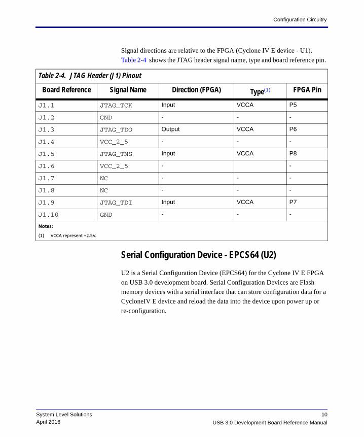
Signal directions are relative to the FPGA (Cyclone IV E device - U1). Table 2-4 shows the JTAG header signal name, type and board reference pin.
Serial Configuration Device - EPCS64 (U2)
U2 is a Serial Configuration Device (EPCS64) for the Cyclone IV E FPGA
on USB 3.0 development board. Serial Configuration Devices are Flash
memory devices with a serial interface that can store configuration data for a
CycloneIV E device and reload the data into the device upon power up or re-configuration.
Table 2-4. JTAG Header (J1) Pinout
Board Reference Signal Name Direction (FPGA) Type(1) FPGA Pin
J1.1 JTAG_TCK Input VCCA P5
J1.2 GND - - -
J1.3 JTAG_TDO Output VCCA P6
J1.4 VCC_2_5 - - -
J1.5 JTAG_TMS Input VCCA P8
J1.6 VCC_2_5 - -
J1.7 NC - - -
J1.8 NC - - -
J1.9 JTAG_TDI Input VCCA P7
J1.10 GND - - -
Notes:
(1) VCCA represent +2.5V.
10
USB 3.0 Development Board Reference Manual
System Level SolutionsApril 2016
Memory Device
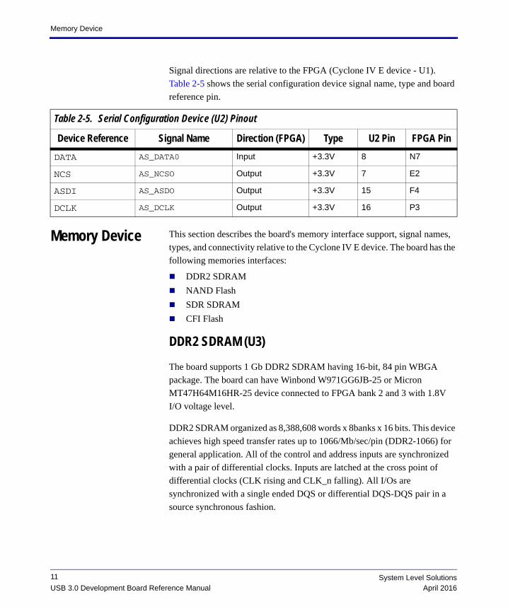
Signal directions are relative to the FPGA (Cyclone IV E device - U1). Table 2-5 shows the serial configuration device signal name, type and board
reference pin.
Memory Device This section describes the board's memory interface support, signal names,
types, and connectivity relative to the Cyclone IV E device. The board has the
following memories interfaces:
DDR2 SDRAM
NAND Flash
SDR SDRAM
CFI Flash
DDR2 SDRAM (U3)
The board supports 1 Gb DDR2 SDRAM having 16-bit, 84 pin WBGA
package. The board can have Winbond W971GG6JB-25 or Micron
MT47H64M16HR-25 device connected to FPGA bank 2 and 3 with 1.8V I/O voltage level.
DDR2 SDRAM organized as 8,388,608 words x 8banks x 16 bits. This device
achieves high speed transfer rates up to 1066/Mb/sec/pin (DDR2-1066) for
general application. All of the control and address inputs are synchronized
with a pair of differential clocks. Inputs are latched at the cross point of
differential clocks (CLK rising and CLK_n falling). All I/Os are
synchronized with a single ended DQS or differential DQS-DQS pair in a
source synchronous fashion.
Table 2-5. Serial Configuration Device (U2) Pinout
Device Reference Signal Name Direction (FPGA) Type U2 Pin FPGA Pin
DATA AS_DATA0 Input +3.3V 8 N7
NCS AS_NCSO Output +3.3V 7 E2
ASDI AS_ASDO Output +3.3V 15 F4
DCLK AS_DCLK Output +3.3V 16 P3
11 System Level SolutionsApril 2016USB 3.0 Development Board Reference Manual
Memory Device
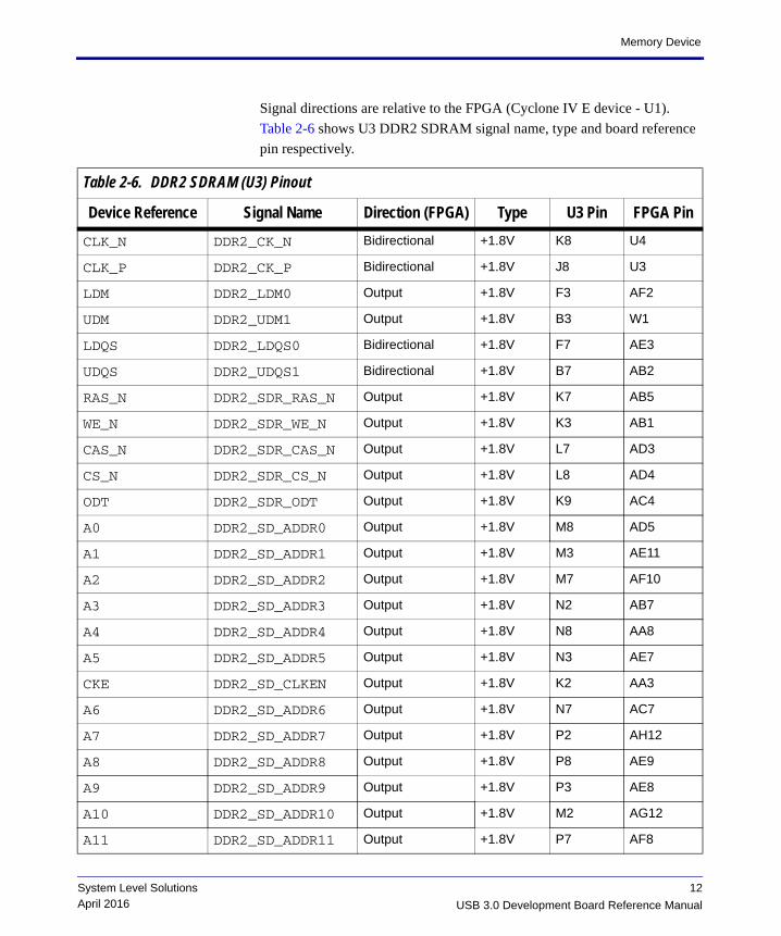
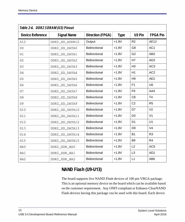
Signal directions are relative to the FPGA (Cyclone IV E device - U1). Table 2-6 shows U3 DDR2 SDRAM signal name, type and board reference
pin respectively.
Table 2-6. DDR2 SDRAM (U3) Pinout
Device Reference Signal Name Direction (FPGA) Type U3 Pin FPGA Pin
CLK_N DDR2_CK_N Bidirectional +1.8V K8 U4
CLK_P DDR2_CK_P Bidirectional +1.8V J8 U3
LDM DDR2_LDM0 Output +1.8V F3 AF2
UDM DDR2_UDM1 Output +1.8V B3 W1
LDQS DDR2_LDQS0 Bidirectional +1.8V F7 AE3
UDQS DDR2_UDQS1 Bidirectional +1.8V B7 AB2
RAS_N DDR2_SDR_RAS_N Output +1.8V K7 AB5
WE_N DDR2_SDR_WE_N Output +1.8V K3 AB1
CAS_N DDR2_SDR_CAS_N Output +1.8V L7 AD3
CS_N DDR2_SDR_CS_N Output +1.8V L8 AD4
ODT DDR2_SDR_ODT Output +1.8V K9 AC4
A0 DDR2_SD_ADDR0 Output +1.8V M8 AD5
A1 DDR2_SD_ADDR1 Output +1.8V M3 AE11
A2 DDR2_SD_ADDR2 Output +1.8V M7 AF10
A3 DDR2_SD_ADDR3 Output +1.8V N2 AB7
A4 DDR2_SD_ADDR4 Output +1.8V N8 AA8
A5 DDR2_SD_ADDR5 Output +1.8V N3 AE7
CKE DDR2_SD_CLKEN Output +1.8V K2 AA3
A6 DDR2_SD_ADDR6 Output +1.8V N7 AC7
A7 DDR2_SD_ADDR7 Output +1.8V P2 AH12
A8 DDR2_SD_ADDR8 Output +1.8V P8 AE9
A9 DDR2_SD_ADDR9 Output +1.8V P3 AE8
A10 DDR2_SD_ADDR10 Output +1.8V M2 AG12
A11 DDR2_SD_ADDR11 Output +1.8V P7 AF8
12
USB 3.0 Development Board Reference Manual
System Level SolutionsApril 2016
Memory Device
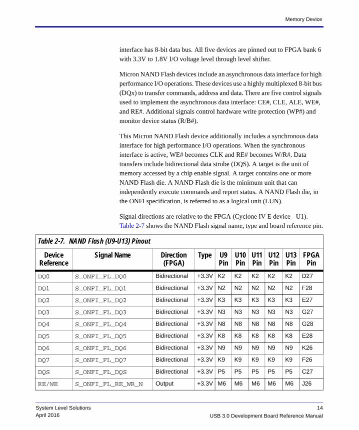
NAND Flash (U9-U13)
The board supports five NAND Flash devices of 100 pin VBGA package.
This is an optional memory device on the board which can be available based
on the customer requirement. Any ONFI compliant or Enhance ClearNAND
Flash devices having this package cna be used with this board. Each device
A12 DDR2_SD_ADDR12 Output +1.8V R2 AE12
D0 DDR2_SD_DATA0 Bidirectional +1.8V G8 AC1
D1 DDR2_SD_DATA1 Bidirectional +1.8V G2 AB3
D2 DDR2_SD_DATA2 Bidirectional +1.8V H7 AD2
D3 DDR2_SD_DATA3 Bidirectional +1.8V H3 AC3
D4 DDR2_SD_DATA4 Bidirectional +1.8V H1 AC2
D5 DDR2_SD_DATA5 Bidirectional +1.8V H9 AE2
D6 DDR2_SD_DATA6 Bidirectional +1.8V F1 U6
D7 DDR2_SD_DATA7 Bidirectional +1.8V F9 AA4
D8 DDR2_SD_DATA8 Bidirectional +1.8V C8 T4
D9 DDR2_SD_DATA9 Bidirectional +1.8V C2 R5
D10 DDR2_SD_DATA10 Bidirectional +1.8V D7 V2
D11 DDR2_SD_DATA11 Bidirectional +1.8V D3 V1
D12 DDR2_SD_DATA12 Bidirectional +1.8V D1 U1
D13 DDR2_SD_DATA13 Bidirectional +1.8V D9 V4
D14 DDR2_SD_DATA14 Bidirectional +1.8V B1 R3
D15 DDR2_SD_DATA15 Bidirectional +1.8V B9 R4
BA0 DDR2_SDR_BA0 Bidirectional +1.8V L2 AC5
BA1 DDR2_SDR_BA1 Bidirectional +1.8V L3 AD1
BA2 DDR2_SDR_BA2 Bidirectional +1.8V L1 AB6
Table 2-6. DDR2 SDRAM (U3) Pinout
Device Reference Signal Name Direction (FPGA) Type U3 Pin FPGA Pin
13 System Level SolutionsApril 2016USB 3.0 Development Board Reference Manual
Memory Device
interface has 8-bit data bus. All five devices are pinned out to FPGA bank 6
with 3.3V to 1.8V I/O voltage level through level shifter.
Micron NAND Flash devices include an asynchronous data interface for high
performance I/O operations. These devices use a highly multiplexed 8-bit bus
(DQx) to transfer commands, address and data. There are five control signals
used to implement the asynchronous data interface: CE#, CLE, ALE, WE#,
and RE#. Additional signals control hardware write protection (WP#) and
monitor device status (R/B#).
This Micron NAND Flash device additionally includes a synchronous data
interface for high performance I/O operations. When the synchronous
interface is active, WE# becomes CLK and RE# becomes W/R#. Data
transfers include bidirectional data strobe (DQS). A target is the unit of
memory accessed by a chip enable signal. A target contains one or more
NAND Flash die. A NAND Flash die is the minimum unit that can
independently execute commands and report status. A NAND Flash die, in
the ONFI specification, is referred to as a logical unit (LUN).
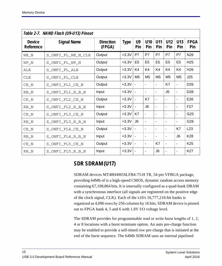
Signal directions are relative to the FPGA (Cyclone IV E device - U1). Table 2-7 shows the NAND Flash signal name, type and board reference pin.
Table 2-7. NAND Flash (U9-U13) Pinout
DeviceReference
Signal Name Direction (FPGA)
Type U9 Pin
U10 Pin
U11 Pin
U12 Pin
U13Pin
FPGA Pin
DQ0 S_ONFI_FL_DQ0 Bidirectional +3.3V K2 K2 K2 K2 K2 D27
DQ1 S_ONFI_FL_DQ1 Bidirectional +3.3V N2 N2 N2 N2 N2 F28
DQ2 S_ONFI_FL_DQ2 Bidirectional +3.3V K3 K3 K3 K3 K3 E27
DQ3 S_ONFI_FL_DQ3 Bidirectional +3.3V N3 N3 N3 N3 N3 G27
DQ4 S_ONFI_FL_DQ4 Bidirectional +3.3V N8 N8 N8 N8 N8 G28
DQ5 S_ONFI_FL_DQ5 Bidirectional +3.3V K8 K8 K8 K8 K8 E28
DQ6 S_ONFI_FL_DQ6 Bidirectional +3.3V N9 N9 N9 N9 N9 K26
DQ7 S_ONFI_FL_DQ7 Bidirectional +3.3V K9 K9 K9 K9 K9 F26
DQS S_ONFI_FL_DQS Bidirectional +3.3V P5 P5 P5 P5 P5 C27
RE/WE S_ONFI_FL_RE_WR_N Output +3.3V M6 M6 M6 M6 M6 J26
14
USB 3.0 Development Board Reference Manual
System Level SolutionsApril 2016
Memory Device
SDR SDRAM (U17)
SDRAM devices MT48H4M16LFB4-75:H TR, 54 pin VFBGA package,
providing 64Mb of is a high-speed CMOS, dynamic random access memory
containing 67,108,864 bits. It is internally configured as a quad-bank DRAM
with a synchronous interface (all signals are registered on the positive edge
of the clock signal, CLK). Each of the x16's 16,777,216-bit banks is
organized as 4,096 rows by 256 columns by 16 bits. SDRAM device is pinned
out to FPGA bank 4, 5 and 6 with 1.8V I/O voltage level.
The SDRAM provides for programmable read or write burst lengths of 1, 2,
4 or 8 locations with a burst terminate option. An auto pre-charge function
may be enabled to provide a self-timed row pre-charge that is initiated at the
end of the burst sequence. The 64Mb SDRAM uses an internal pipelined
WE_N S_ONFI_FL_WE_N_CLK Output +3.3V P7 P7 P7 P7 P7 N26
WP_N S_ONFI_FL_WP_N Output +3.3V E5 E5 E5 E5 E5 H25
ALE S_ONFI_FL_ALE Output +3.3V K4 K4 K4 K4 K4 H26
CLE S_ONFI_FL_CLE Output +3.3V M5 M5 M5 M5 M5 J25
CE_N S_ONFI_FL1_CE_N Output +3.3V - - - K7 - D26
RB_N S_ONFI_FL1_R_B_N Input +3.3V - - - J6 - D28
CE_N S_ONFI_FL2_CE_N Output +3.3V - K7 - - - E26
RB_N S_ONFI_FL2_R_B_N Input +3.3V - J6 - - - F27
CE_N S_ONFI_FL3_CE_N Output +3.3V K7 - - - - G25
RB_N S_ONFI_FL3_R_B_N Input +3.3V J6 - - - - G26
CE_N S_ONFI_FL4_CE_N Output +3.3V - - - - K7 L23
RB_N S_ONFI_FL4_R_B_N Input +3.3V - - - - J6 K28
CE_N S_ONFI_FL5_CE_N Output +3.3V - - K7 - - K25
RB_N S_ONFI_FL5_R_B_N Input +3.3V - - J6 - - K27
Table 2-7. NAND Flash (U9-U13) Pinout
DeviceReference
Signal Name Direction (FPGA)
Type U9 Pin
U10 Pin
U11 Pin
U12 Pin
U13Pin
FPGA Pin
15 System Level SolutionsApril 2016USB 3.0 Development Board Reference Manual
Memory Device
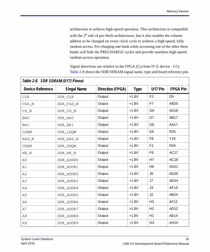
architecture to achieve high-speed operation. This architecture is compatible
with the 2n rule of pre-fetch architectures, but it also enables the column
address to be changed on every clock cycle to achieve a high-speed, fully
random access. Pre-charging one bank while accessing one of the other three
banks will hide the PRECHARGE cycles and provide seamless high-speed,
random-access operation.
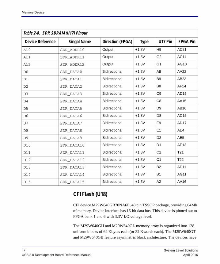
Signal directions are relative to the FPGA (Cyclone IV E device - U1). Table 2-8 shows the SDR SDRAM signal name, type and board reference pin.
Table 2-8. SDR SDRAM (U17) Pinout
Device Reference Singal Name Direction (FPGA) Type U17 Pin FPGA Pin
CLK SDR_CLK Output +1.8V F2 D5
CAS_N SDR_CAS_N Output +1.8V F7 AB20
CS_N SDR_CS_N Output +1.8V G9 AD18
BA0 SDR_BA0 Output +1.8V G7 AB17
BA1 SDR_BA1 Output +1.8V G8 AA17
LDQM SDR_LDQM Output +1.8V E8 R25
RAS_N SDR_RAS_N Output +1.8V F8 Y19
UDQM SDR_UDQM Output +1.8V F1 R24
WE_N SDR_WE_N Output +1.8V F9 AC17
A0 SDR_ADDR0 Output +1.8V H7 AC18
A1 SDR_ADDR1 Output +1.8V H8 AD21
A2 SDR_ADDR2 Output +1.8V J8 AD25
A3 SDR_ADDR3 Output +1.8V J7 AD24
A4 SDR_ADDR4 Output +1.8V J3 AF13
A5 SDR_ADDR5 Output +1.8V J2 AB24
A6 SDR_ADDR6 Output +1.8V H3 AF12
A7 SDR_ADDR7 Output +1.8V H2 AD12
A8 SDR_ADDR8 Output +1.8V H1 AE14
A9 SDR_ADDR9 Output +1.8V G3 AH10
16
USB 3.0 Development Board Reference Manual
System Level SolutionsApril 2016
Memory Device
CFI Flash (U18)
CFI device M29W640GB70NA6E, 48 pin TSSOP package, providing 64Mb
of memory. Device interface has 16-bit data bus. This device is pinned out to
FPGA bank 1 and 6 with 3.3V I/O voltage level.
The M29W640GH and M29W640GL memory array is organized into 128
uniform blocks of 64 Kbytes each (or 32 Kwords each). The M29W640GT
and M29W640GB feature asymmetric block architecture. The devices have
A10 SDR_ADDR10 Output +1.8V H9 AC21
A11 SDR_ADDR11 Output +1.8V G2 AC11
A12 SDR_ADDR12 Output +1.8V G1 AG10
D0 SDR_DATA0 Bidirectional +1.8V A8 AA22
D1 SDR_DATA1 Bidirectional +1.8V B9 AB23
D2 SDR_DATA2 Bidirectional +1.8V B8 AF14
D3 SDR_DATA3 Bidirectional +1.8V C9 AD15
D4 SDR_DATA4 Bidirectional +1.8V C8 AA15
D5 SDR_DATA5 Bidirectional +1.8V D9 AB16
D6 SDR_DATA6 Bidirectional +1.8V D8 AC15
D7 SDR_DATA7 Bidirectional +1.8V E9 AD17
D8 SDR_DATA8 Bidirectional +1.8V E1 AE4
D9 SDR_DATA9 Bidirectional +1.8V D2 AE5
D10 SDR_DATA10 Bidirectional +1.8V D1 AE13
D11 SDR_DATA11 Bidirectional +1.8V C2 T21
D12 SDR_DATA12 Bidirectional +1.8V C1 T22
D13 SDR_DATA13 Bidirectional +1.8V B2 AD11
D14 SDR_DATA14 Bidirectional +1.8V B1 AG11
D15 SDR_DATA15 Bidirectional +1.8V A2 AA16
Table 2-8. SDR SDRAM (U17) Pinout
Device Reference Singal Name Direction (FPGA) Type U17 Pin FPGA Pin
17 System Level SolutionsApril 2016USB 3.0 Development Board Reference Manual
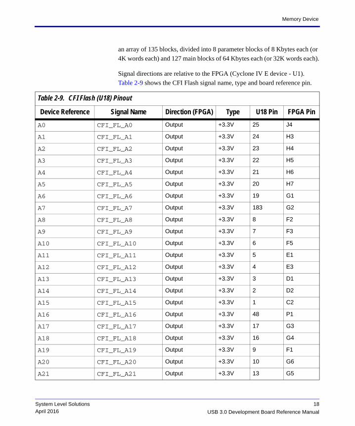
Memory Device
an array of 135 blocks, divided into 8 parameter blocks of 8 Kbytes each (or
4K words each) and 127 main blocks of 64 Kbytes each (or 32K words each).
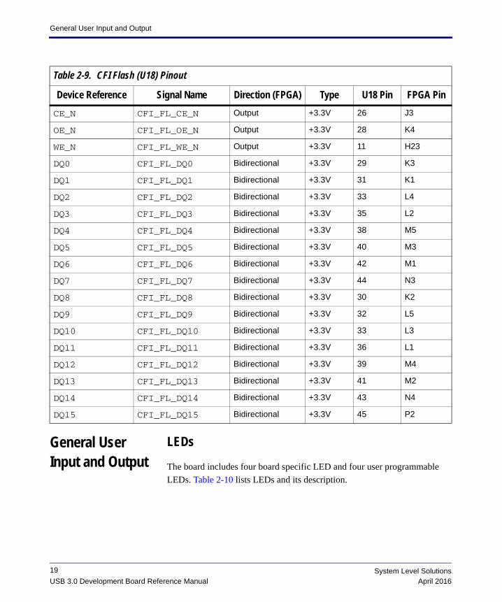
Signal directions are relative to the FPGA (Cyclone IV E device - U1). Table 2-9 shows the CFI Flash signal name, type and board reference pin.
Table 2-9. CFI Flash (U18) Pinout
Device Reference Signal Name Direction (FPGA) Type U18 Pin FPGA Pin
A0 CFI_FL_A0 Output +3.3V 25 J4
A1 CFI_FL_A1 Output +3.3V 24 H3
A2 CFI_FL_A2 Output +3.3V 23 H4
A3 CFI_FL_A3 Output +3.3V 22 H5
A4 CFI_FL_A4 Output +3.3V 21 H6
A5 CFI_FL_A5 Output +3.3V 20 H7
A6 CFI_FL_A6 Output +3.3V 19 G1
A7 CFI_FL_A7 Output +3.3V 183 G2
A8 CFI_FL_A8 Output +3.3V 8 F2
A9 CFI_FL_A9 Output +3.3V 7 F3
A10 CFI_FL_A10 Output +3.3V 6 F5
A11 CFI_FL_A11 Output +3.3V 5 E1
A12 CFI_FL_A12 Output +3.3V 4 E3
A13 CFI_FL_A13 Output +3.3V 3 D1
A14 CFI_FL_A14 Output +3.3V 2 D2
A15 CFI_FL_A15 Output +3.3V 1 C2
A16 CFI_FL_A16 Output +3.3V 48 P1
A17 CFI_FL_A17 Output +3.3V 17 G3
A18 CFI_FL_A18 Output +3.3V 16 G4
A19 CFI_FL_A19 Output +3.3V 9 F1
A20 CFI_FL_A20 Output +3.3V 10 G6
A21 CFI_FL_A21 Output +3.3V 13 G5
18
USB 3.0 Development Board Reference Manual
System Level SolutionsApril 2016
General User Input and Output
General User Input and Output
LEDs
The board includes four board specific LED and four user programmable
LEDs. Table 2-10 lists LEDs and its description.
CE_N CFI_FL_CE_N Output +3.3V 26 J3
OE_N CFI_FL_OE_N Output +3.3V 28 K4
WE_N CFI_FL_WE_N Output +3.3V 11 H23
DQ0 CFI_FL_DQ0 Bidirectional +3.3V 29 K3
DQ1 CFI_FL_DQ1 Bidirectional +3.3V 31 K1
DQ2 CFI_FL_DQ2 Bidirectional +3.3V 33 L4
DQ3 CFI_FL_DQ3 Bidirectional +3.3V 35 L2
DQ4 CFI_FL_DQ4 Bidirectional +3.3V 38 M5
DQ5 CFI_FL_DQ5 Bidirectional +3.3V 40 M3
DQ6 CFI_FL_DQ6 Bidirectional +3.3V 42 M1
DQ7 CFI_FL_DQ7 Bidirectional +3.3V 44 N3
DQ8 CFI_FL_DQ8 Bidirectional +3.3V 30 K2
DQ9 CFI_FL_DQ9 Bidirectional +3.3V 32 L5
DQ10 CFI_FL_DQ10 Bidirectional +3.3V 33 L3
DQ11 CFI_FL_DQ11 Bidirectional +3.3V 36 L1
DQ12 CFI_FL_DQ12 Bidirectional +3.3V 39 M4
DQ13 CFI_FL_DQ13 Bidirectional +3.3V 41 M2
DQ14 CFI_FL_DQ14 Bidirectional +3.3V 43 N4
DQ15 CFI_FL_DQ15 Bidirectional +3.3V 45 P2
Table 2-9. CFI Flash (U18) Pinout
Device Reference Signal Name Direction (FPGA) Type U18 Pin FPGA Pin
19 System Level SolutionsApril 2016USB 3.0 Development Board Reference Manual
General User Input and Output
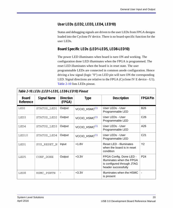
User LEDs (LED2, LED3, LED4, LED10)
Status and debugging signals are driven to the user LEDs from FPGA designs
loaded into the Cyclone IV device. There is no board-specific function for the
user LEDs.
Board Specific LEDs (LED1-LED5, LED8-LED10)
The power LED illuminates when board is turn ON and working. The
configuration done LED illuminates when the FPGA is programmed. The
reset LED illuminates when the board is in reset state. The user
programmable LEDs are connected in common anode configuration. Hence
driving a low signal (logic "0") on LED pin will turn ON the corresponding
LED. Signal directions are relative to the FPGA (Cyclone IV E device - U1).
Table 2-10 lists LEDs pinout.
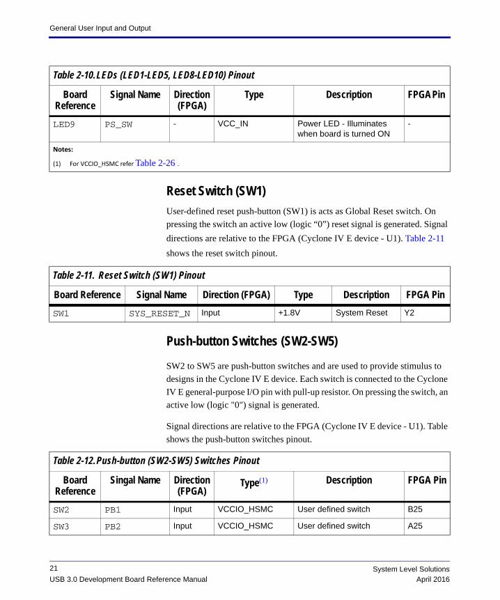
Table 2-10.LEDs (LED1-LED5, LED8-LED10) Pinout
Board Reference
Signal Name Direction (FPGA)
Type Description FPGA Pin
LED2 STATUS_LED1 Output VCCIO_HSMC(1) User LEDs - User Programmable LED
B26
LED3 STATUS_LED2 Output VCCIO_HSMC(1) User LEDs - User Programmable LED
C26
LED4 STATUS_LED3 Output VCCIO_HSMC(1) User LEDs - User Programmable LED
A26
LED10 STATUS_LED4 Output VCCIO_HSMC(1) User LEDs - User Programmable LED
C21
LED1 SYS_RESET_N Input +1.8V Reset LED - Illuminates when the board is in reset condition
Y2
LED5 CONF_DONE Output +3.3V FPGA Config. Done LED - Illuminates when the FPGA is configured through JTAG header successfully
P24
LED8 HSMC_PSNTN - +3.3V Illuminates when the HSMC is present
-
20
USB 3.0 Development Board Reference Manual
System Level SolutionsApril 2016
General User Input and Output
Reset Switch (SW1)
User-defined reset push-button (SW1) is acts as Global Reset switch. On
pressing the switch an active low (logic “0”) reset signal is generated. Signal
directions are relative to the FPGA (Cyclone IV E device - U1). Table 2-11
shows the reset switch pinout.
Push-button Switches (SW2-SW5)
SW2 to SW5 are push-button switches and are used to provide stimulus to
designs in the Cyclone IV E device. Each switch is connected to the Cyclone
IV E general-purpose I/O pin with pull-up resistor. On pressing the switch, an
active low (logic "0") signal is generated.
Signal directions are relative to the FPGA (Cyclone IV E device - U1). Table
shows the push-button switches pinout.
LED9 PS_SW - VCC_IN Power LED - Illuminates when board is turned ON
-
Notes:
(1) For VCCIO_HSMC refer Table 2-26 .
Table 2-10.LEDs (LED1-LED5, LED8-LED10) Pinout
Board Reference
Signal Name Direction (FPGA)
Type Description FPGA Pin
Table 2-11. Reset Switch (SW1) Pinout
Board Reference Signal Name Direction (FPGA) Type Description FPGA Pin
SW1 SYS_RESET_N Input +1.8V System Reset Y2
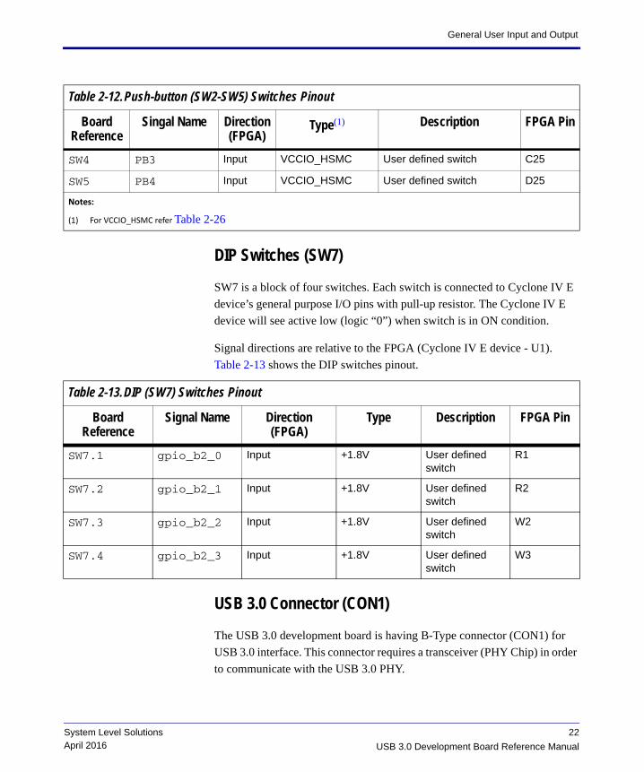
Table 2-12.Push-button (SW2-SW5) Switches Pinout
Board Reference
Singal Name Direction (FPGA)
Type(1) Description FPGA Pin
SW2 PB1 Input VCCIO_HSMC User defined switch B25
SW3 PB2 Input VCCIO_HSMC User defined switch A25
21 System Level SolutionsApril 2016USB 3.0 Development Board Reference Manual
General User Input and Output
DIP Switches (SW7)
SW7 is a block of four switches. Each switch is connected to Cyclone IV E
device’s general purpose I/O pins with pull-up resistor. The Cyclone IV E
device will see active low (logic “0”) when switch is in ON condition.
Signal directions are relative to the FPGA (Cyclone IV E device - U1). Table 2-13 shows the DIP switches pinout.
USB 3.0 Connector (CON1)
The USB 3.0 development board is having B-Type connector (CON1) for
USB 3.0 interface. This connector requires a transceiver (PHY Chip) in order
to communicate with the USB 3.0 PHY.
SW4 PB3 Input VCCIO_HSMC User defined switch C25
SW5 PB4 Input VCCIO_HSMC User defined switch D25
Notes:
(1) For VCCIO_HSMC refer Table 2-26
Table 2-12.Push-button (SW2-SW5) Switches Pinout
Board Reference
Singal Name Direction (FPGA)
Type(1) Description FPGA Pin
Table 2-13.DIP (SW7) Switches Pinout
BoardReference
Signal Name Direction (FPGA)
Type Description FPGA Pin
SW7.1 gpio_b2_0 Input +1.8V User defined switch
R1
SW7.2 gpio_b2_1 Input +1.8V User defined switch
R2
SW7.3 gpio_b2_2 Input +1.8V User defined switch
W2
SW7.4 gpio_b2_3 Input +1.8V User defined switch
W3
22
USB 3.0 Development Board Reference Manual
System Level SolutionsApril 2016
General User Input and Output
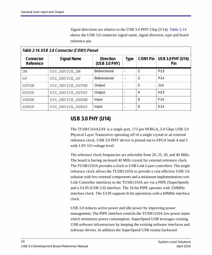
Signal directions are relative to the USB 3.0 PHY Chip (U14). Table 2-14
shows the USB 3.0 connector signal name, signal direction, type and board
reference pin.
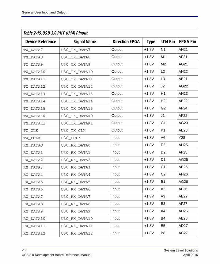
USB 3.0 PHY (U14)
The TUSB1310AZAY is a single port, 175 pin NFBGA, 5.0 Gbps USB 3.0
Physical Layer Transceiver operating off of a single crystal or an external
reference clock. USB 3.0 PHY device is pinned out to FPGA bank 4 and 5
with 1.8V I/O voltage level.
The reference clock frequencies are selectable from 20, 25, 30, and 40 MHz.
The board is having on-board 40 MHz crystal for external reference clock.
The TUSB1310A provides a clock to USB Link Layer controllers. The single
reference clock allows the TUSB1310A to provide a cost effective USB 3.0
solution with few external components and a minimum implementation cost.
Link Controller interfaces to the TUSB1310A are via a PIPE (SuperSpeed)
and a ULPI (USB 2.0) interface. The 16-bit PIPE operates with 250MHz
interface clock. The ULPI supports 8-bit operations with a 60MHz interface
clock.
USB 3.0 reduces active power and idle power by improving power
management. The PIPE interface controls the TUSB1310A low power states
which minimizes power consumption. SuperSpeed USB leverages existing
USB software infrastructure by keeping the existing software interfaces and
software drivers. In addition the SuperSpeed USB retains backward
Table 2-14.USB 3.0 Connector (CON1) Pinout
ConnectorReference
Signal Name Direction(USB 3.0 PHY)
Type CON1 Pin USB 3.0 PHY (U14) Pin
DM U30_DEVICE_DM Bidirectional - 2 P13
DP U30_DEVICE_DP Bidirectional - 3 P14
SSTXN U30_DEVICE_SSTXN Output - 5 J14
SSTXP U30_DEVICE_SSTXP Output - 6 H14
SSRXN U30_DEVICE_SSRXN Input - 8 F14
SSRXP U30_DEVICE_SSRXP Input - 9 E14
23 System Level SolutionsApril 2016USB 3.0 Development Board Reference Manual
General User Input and Output
compatibility at the Type A connector with USB 2.0 based PCs and with USB 2.0 cables.
The single reference clock allows the TUSB1310A to provide a cost effective
USB 3.0 solution with few external components and a minimum
implementation cost.
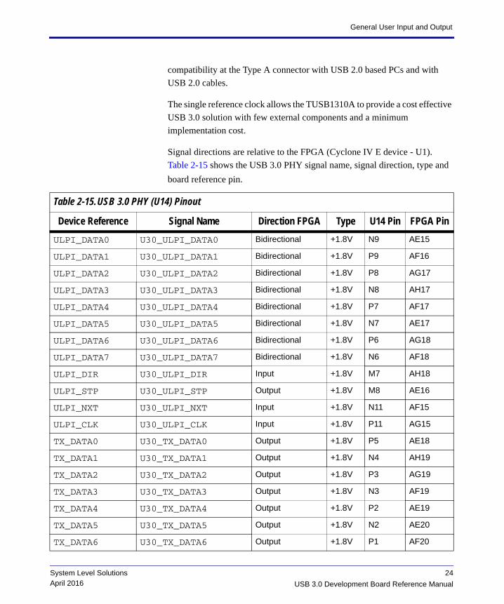
Signal directions are relative to the FPGA (Cyclone IV E device - U1). Table 2-15 shows the USB 3.0 PHY signal name, signal direction, type and
board reference pin.
Table 2-15.USB 3.0 PHY (U14) Pinout
Device Reference Signal Name Direction FPGA Type U14 Pin FPGA Pin
ULPI_DATA0 U30_ULPI_DATA0 Bidirectional +1.8V N9 AE15
ULPI_DATA1 U30_ULPI_DATA1 Bidirectional +1.8V P9 AF16
ULPI_DATA2 U30_ULPI_DATA2 Bidirectional +1.8V P8 AG17
ULPI_DATA3 U30_ULPI_DATA3 Bidirectional +1.8V N8 AH17
ULPI_DATA4 U30_ULPI_DATA4 Bidirectional +1.8V P7 AF17
ULPI_DATA5 U30_ULPI_DATA5 Bidirectional +1.8V N7 AE17
ULPI_DATA6 U30_ULPI_DATA6 Bidirectional +1.8V P6 AG18
ULPI_DATA7 U30_ULPI_DATA7 Bidirectional +1.8V N6 AF18
ULPI_DIR U30_ULPI_DIR Input +1.8V M7 AH18
ULPI_STP U30_ULPI_STP Output +1.8V M8 AE16
ULPI_NXT U30_ULPI_NXT Input +1.8V N11 AF15
ULPI_CLK U30_ULPI_CLK Input +1.8V P11 AG15
TX_DATA0 U30_TX_DATA0 Output +1.8V P5 AE18
TX_DATA1 U30_TX_DATA1 Output +1.8V N4 AH19
TX_DATA2 U30_TX_DATA2 Output +1.8V P3 AG19
TX_DATA3 U30_TX_DATA3 Output +1.8V N3 AF19
TX_DATA4 U30_TX_DATA4 Output +1.8V P2 AE19
TX_DATA5 U30_TX_DATA5 Output +1.8V N2 AE20
TX_DATA6 U30_TX_DATA6 Output +1.8V P1 AF20
24
USB 3.0 Development Board Reference Manual
System Level SolutionsApril 2016
General User Input and Output
TX_DATA7 U30_TX_DATA7 Output +1.8V N1 AH21
TX_DATA8 U30_TX_DATA8 Output +1.8V M1 AF21
TX_DATA9 U30_TX_DATA9 Output +1.8V M2 AG21
TX_DATA10 U30_TX_DATA10 Output +1.8V L2 AH22
TX_DATA11 U30_TX_DATA11 Output +1.8V L3 AE21
TX_DATA12 U30_TX_DATA12 Output +1.8V J2 AG22
TX_DATA13 U30_TX_DATA13 Output +1.8V H1 AH23
TX_DATA14 U30_TX_DATA14 Output +1.8V H2 AE22
TX_DATA15 U30_TX_DATA15 Output +1.8V G2 AF24
TX_DATAK0 U30_TX_DATAK0 Output +1.8V J1 AF22
TX_DATAK1 U30_TX_DATAK1 Output +1.8V G1 AG23
TX_CLK U30_TX_CLK Output +1.8V K1 AE23
TX_PCLK U30_PCLK Input +1.8V A6 Y28
RX_DATAO U30_RX_DATA0 Input +1.8V E2 AH25
RX_DATA1 U30_RX_DATA1 Input +1.8V D2 AF25
RX_DATA2 U30_RX_DATA2 Input +1.8V D1 AG25
RX_DATA3 U30_RX_DATA3 Input +1.8V C1 AE25
RX_DATA4 U30_RX_DATA4 Input +1.8V C2 AH26
RX_DATA5 U30_RX_DATA5 Input +1.8V B1 AG26
RX_DATA6 U30_RX_DATA6 Input +1.8V A2 AF26
RX_DATA7 U30_RX_DATA7 Input +1.8V A3 AE27
RX_DATA8 U30_RX_DATA8 Input +1.8V B3 AF27
RX_DATA9 U30_RX_DATA9 Input +1.8V A4 AD26
RX_DATA10 U30_RX_DATA10 Input +1.8V B4 AE28
RX_DATA11 U30_RX_DATA11 Input +1.8V B5 AD27
RX_DATA12 U30_RX_DATA12 Input +1.8V B8 AC27
Table 2-15.USB 3.0 PHY (U14) Pinout
Device Reference Signal Name Direction FPGA Type U14 Pin FPGA Pin
25 System Level SolutionsApril 2016USB 3.0 Development Board Reference Manual
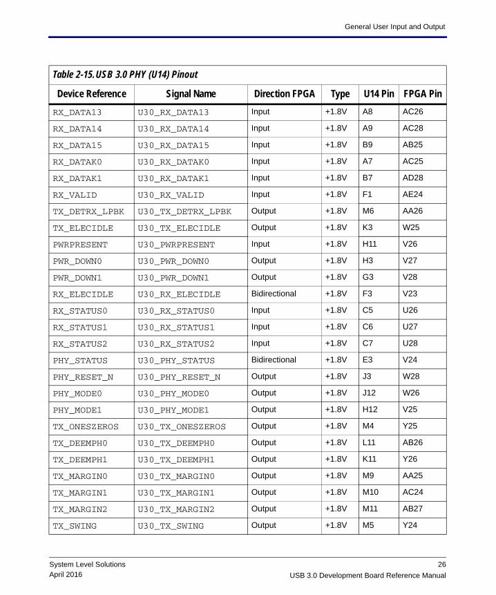
General User Input and Output
RX_DATA13 U30_RX_DATA13 Input +1.8V A8 AC26
RX_DATA14 U30_RX_DATA14 Input +1.8V A9 AC28
RX_DATA15 U30_RX_DATA15 Input +1.8V B9 AB25
RX_DATAK0 U30_RX_DATAK0 Input +1.8V A7 AC25
RX_DATAK1 U30_RX_DATAK1 Input +1.8V B7 AD28
RX_VALID U30_RX_VALID Input +1.8V F1 AE24
TX_DETRX_LPBK U30_TX_DETRX_LPBK Output +1.8V M6 AA26
TX_ELECIDLE U30_TX_ELECIDLE Output +1.8V K3 W25
PWRPRESENT U30_PWRPRESENT Input +1.8V H11 V26
PWR_DOWN0 U30_PWR_DOWN0 Output +1.8V H3 V27
PWR_DOWN1 U30_PWR_DOWN1 Output +1.8V G3 V28
RX_ELECIDLE U30_RX_ELECIDLE Bidirectional +1.8V F3 V23
RX_STATUS0 U30_RX_STATUS0 Input +1.8V C5 U26
RX_STATUS1 U30_RX_STATUS1 Input +1.8V C6 U27
RX_STATUS2 U30_RX_STATUS2 Input +1.8V C7 U28
PHY_STATUS U30_PHY_STATUS Bidirectional +1.8V E3 V24
PHY_RESET_N U30_PHY_RESET_N Output +1.8V J3 W28
PHY_MODE0 U30_PHY_MODE0 Output +1.8V J12 W26
PHY_MODE1 U30_PHY_MODE1 Output +1.8V H12 V25
TX_ONESZEROS U30_TX_ONESZEROS Output +1.8V M4 Y25
TX_DEEMPH0 U30_TX_DEEMPH0 Output +1.8V L11 AB26
TX_DEEMPH1 U30_TX_DEEMPH1 Output +1.8V K11 Y26
TX_MARGIN0 U30_TX_MARGIN0 Output +1.8V M9 AA25
TX_MARGIN1 U30_TX_MARGIN1 Output +1.8V M10 AC24
TX_MARGIN2 U30_TX_MARGIN2 Output +1.8V M11 AB27
TX_SWING U30_TX_SWING Output +1.8V M5 Y24
Table 2-15.USB 3.0 PHY (U14) Pinout
Device Reference Signal Name Direction FPGA Type U14 Pin FPGA Pin
26
USB 3.0 Development Board Reference Manual
System Level SolutionsApril 2016
General User Input and Output
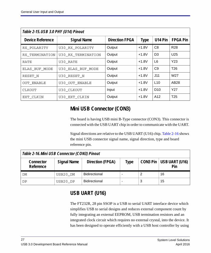
Mini USB Connector (CON3)
The board is having USB mini B-Type connector (CON3). This connector is
connected with the USB UART chip in order to communicate with the UART.
Signal directions are relative to the USB UART (U16) chip. Table 2-16 shows
the mini USB connector signal name, signal direction, type and board
reference pin.
USB UART (U16)
The FT232R, 28 pin SSOP is a USB to serial UART interface device which
simplifies USB to serial designs and reduces external component count by
fully integrating an external EEPROM, USB termination resistors and an
integrated clock circuit which requires no external crystal, into the device. It
has been designed to operate efficiently with a USB host controller by using
RX_POLARITY U30_RX_POLARITY Output +1.8V C8 R28
RX_TERMINATION U30_RX_TERMINATION Output +1.8V D3 U25
RATE U30_RATE Output +1.8V L6 Y23
ELAS_BUF_MODE U30_ELAS_BUF_MODE Output +1.8V C9 T26
RESET_N U30_RESET_N Output +1.8V J11 W27
OUT_ENABLE U30_OUT_ENABLE Output +1.8V L10 AB28
CLKOUT U30_CLKOUT Input +1.8V D10 Y27
EXT_CLKIN U30_EXT_CLKIN Output +1.8V A12 T25
Table 2-15.USB 3.0 PHY (U14) Pinout
Device Reference Signal Name Direction FPGA Type U14 Pin FPGA Pin
Table 2-16.Mini USB Connector (CON3) Pinout
Connector Reference
Signal Name Direction (FPGA) Type CON3 Pin USB UART (U16) Pin
DM USB20_DM Bidirectional - 2 16
DP USB20_DP Bidirectional - 3 15
27 System Level SolutionsApril 2016USB 3.0 Development Board Reference Manual
General User Input and Output
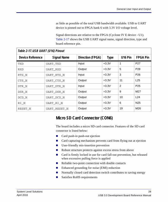
as little as possible of the total USB bandwidth available. USB to UART
device is pinned out to FPGA bank 6 with 3.3V I/O voltage level.
Signal directions are relative to the FPGA (Cyclone IV E device - U1). Table 2-17 shows the USB UART signal name, signal direction, type and
board reference pin.
Micro SD Card Connector (CON6)
The board includes a micro SD card connector. Features of the SD card
connector is listed below:
Card push-in push-out ejection
Card capturing mechanism prevents card from flying out at ejection
User-friendly mis-insertion prevention
Robust structure protects against excess stress from above
Card is firmly locked in use for card fall-out prevention, but released when excessive pulling force is applied
Reliable two-point connection with double contacts
Enhanced grounding for noise (EMI) reduction
Normally closed card detection switch contributes to saving energy
Satisfies RoHS requirements
Table 2-17.USB UART (U16) Pinout
Device Reference Signal Name Direction (FPGA) Type U16 Pin FPGA Pin
TXD UART_TXD Input +3.3V 1 P27
RXD UART_RXD Output +3.3V 5 P28
RTS_N UART_RTS_N Input +3.3V 3 P26
CTS_N UART_CTS_N Output +3.3V 11 L25
DTR_N UART_DTR_N Input +3.3V 2 P25
DSR_N UART_DSR_N Output +3.3V 9 M27
DCD_N UART_DCD_N Output +3.3V 10 L24
RI_N UART_RI_N Output +3.3V 6 N25
RESET_N UART_RESET_N Output +3.3V 19 M26
28
USB 3.0 Development Board Reference Manual
System Level SolutionsApril 2016
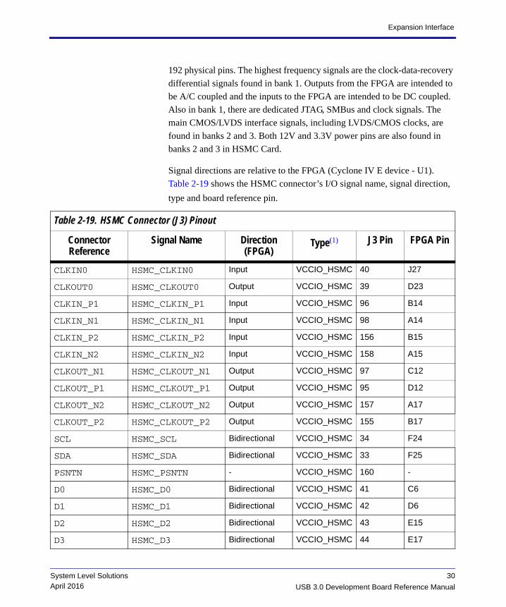
Expansion Interface
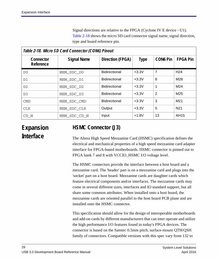
Signal directions are relative to the FPGA (Cyclone IV E device - U1). Table 2-18 shows the micro SD card connector signal name, signal direction,
type and board reference pin.
Expansion Interface
HSMC Connector (J3)
The Altera High Speed Mezzanine Card (HSMC) specification defines the
electrical and mechanical properties of a high speed mezzanine card adapter
interface for FPGA-based motherboards. HSMC connector is pinned out to
FPGA bank 7 and 8 with VCCIO_HSMC I/O voltage level.
The HSMC connectors provide the interface between a host board and a
mezzanine card. The 'header' part is on a mezzanine card and plugs into the
'socket' part on a host board. Mezzanine cards are daughter cards which
feature electrical components and/or interfaces. The mezzanine cards may
come in several different sizes, interfaces and IO standard support, but all
share some common attributes. When installed onto a host board, the
mezzanine cards are oriented parallel to the host board PCB plane and are
installed onto the HSMC connector.
This specification should allow for the design of interoperable motherboards
and add-on cards by different manufacturers that can inter operate and utilize
the high performance I/O features found in today's FPGA devices. The
connector is based on the Samtec 0.5mm pitch, surface-mount QTH/QSH
family of connectors. Compatible versions with this spec vary from 132 to
Table 2-18. Micro SD Card Connector (CON6) Pinout
Connector Reference
Signal Name Direction (FPGA) Type CON6 Pin FPGA Pin
D0 MEM_SDC_D0 Bidirectional +3.3V 7 H24
D1 MEM_SDC_D1 Bidirectional +3.3V 8 M28
D2 MEM_SDC_D2 Bidirectional +3.3V 1 M24
D3 MEM_SDC_D3 Bidirectional +3.3V 2 M25
CMD MEM_SDC_CMD Bidirectional +3.3V 3 M21
CLK MEM_SDC_CLK Output +3.3V 5 N21
CD_N MEM_SDC_CD_N Input +1.8V 13 AH15
29 System Level SolutionsApril 2016USB 3.0 Development Board Reference Manual
Expansion Interface
192 physical pins. The highest frequency signals are the clock-data-recovery
differential signals found in bank 1. Outputs from the FPGA are intended to
be A/C coupled and the inputs to the FPGA are intended to be DC coupled.
Also in bank 1, there are dedicated JTAG, SMBus and clock signals. The
main CMOS/LVDS interface signals, including LVDS/CMOS clocks, are
found in banks 2 and 3. Both 12V and 3.3V power pins are also found in
banks 2 and 3 in HSMC Card.
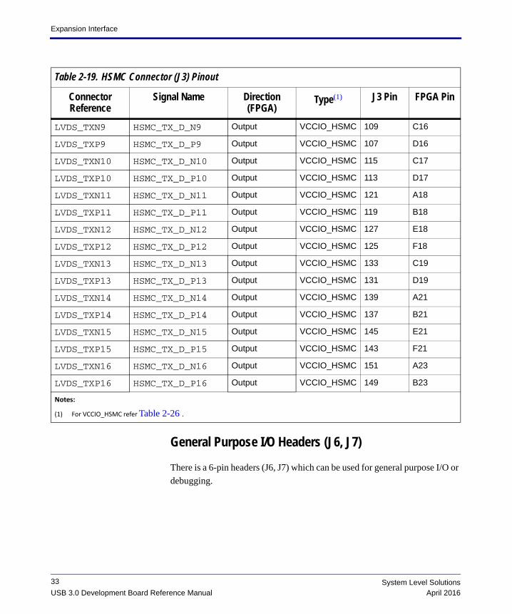
Signal directions are relative to the FPGA (Cyclone IV E device - U1). Table 2-19 shows the HSMC connector’s I/O signal name, signal direction,
type and board reference pin.
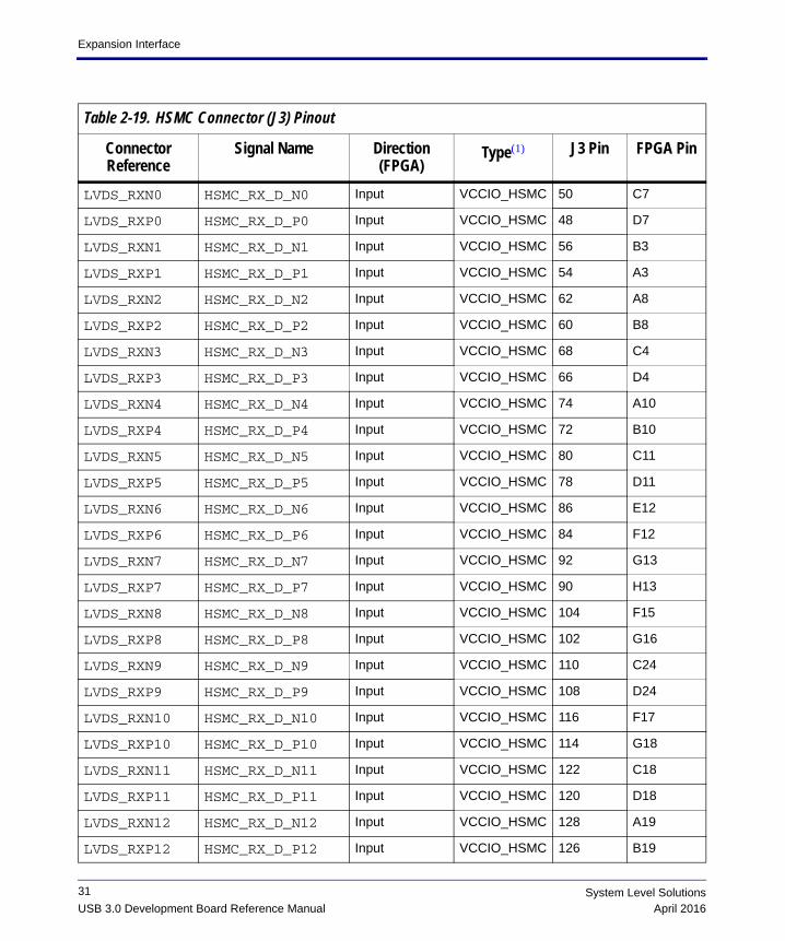
Table 2-19. HSMC Connector (J3) Pinout
Connector Reference
Signal Name Direction (FPGA)
Type(1) J3 Pin FPGA Pin
CLKIN0 HSMC_CLKIN0 Input VCCIO_HSMC 40 J27
CLKOUT0 HSMC_CLKOUT0 Output VCCIO_HSMC 39 D23
CLKIN_P1 HSMC_CLKIN_P1 Input VCCIO_HSMC 96 B14
CLKIN_N1 HSMC_CLKIN_N1 Input VCCIO_HSMC 98 A14
CLKIN_P2 HSMC_CLKIN_P2 Input VCCIO_HSMC 156 B15
CLKIN_N2 HSMC_CLKIN_N2 Input VCCIO_HSMC 158 A15
CLKOUT_N1 HSMC_CLKOUT_N1 Output VCCIO_HSMC 97 C12
CLKOUT_P1 HSMC_CLKOUT_P1 Output VCCIO_HSMC 95 D12
CLKOUT_N2 HSMC_CLKOUT_N2 Output VCCIO_HSMC 157 A17
CLKOUT_P2 HSMC_CLKOUT_P2 Output VCCIO_HSMC 155 B17
SCL HSMC_SCL Bidirectional VCCIO_HSMC 34 F24
SDA HSMC_SDA Bidirectional VCCIO_HSMC 33 F25
PSNTN HSMC_PSNTN - VCCIO_HSMC 160 -
D0 HSMC_D0 Bidirectional VCCIO_HSMC 41 C6
D1 HSMC_D1 Bidirectional VCCIO_HSMC 42 D6
D2 HSMC_D2 Bidirectional VCCIO_HSMC 43 E15
D3 HSMC_D3 Bidirectional VCCIO_HSMC 44 E17
30
USB 3.0 Development Board Reference Manual
System Level SolutionsApril 2016
Expansion Interface
LVDS_RXN0 HSMC_RX_D_N0 Input VCCIO_HSMC 50 C7
LVDS_RXP0 HSMC_RX_D_P0 Input VCCIO_HSMC 48 D7
LVDS_RXN1 HSMC_RX_D_N1 Input VCCIO_HSMC 56 B3
LVDS_RXP1 HSMC_RX_D_P1 Input VCCIO_HSMC 54 A3
LVDS_RXN2 HSMC_RX_D_N2 Input VCCIO_HSMC 62 A8
LVDS_RXP2 HSMC_RX_D_P2 Input VCCIO_HSMC 60 B8
LVDS_RXN3 HSMC_RX_D_N3 Input VCCIO_HSMC 68 C4
LVDS_RXP3 HSMC_RX_D_P3 Input VCCIO_HSMC 66 D4
LVDS_RXN4 HSMC_RX_D_N4 Input VCCIO_HSMC 74 A10
LVDS_RXP4 HSMC_RX_D_P4 Input VCCIO_HSMC 72 B10
LVDS_RXN5 HSMC_RX_D_N5 Input VCCIO_HSMC 80 C11
LVDS_RXP5 HSMC_RX_D_P5 Input VCCIO_HSMC 78 D11
LVDS_RXN6 HSMC_RX_D_N6 Input VCCIO_HSMC 86 E12
LVDS_RXP6 HSMC_RX_D_P6 Input VCCIO_HSMC 84 F12
LVDS_RXN7 HSMC_RX_D_N7 Input VCCIO_HSMC 92 G13
LVDS_RXP7 HSMC_RX_D_P7 Input VCCIO_HSMC 90 H13
LVDS_RXN8 HSMC_RX_D_N8 Input VCCIO_HSMC 104 F15
LVDS_RXP8 HSMC_RX_D_P8 Input VCCIO_HSMC 102 G16
LVDS_RXN9 HSMC_RX_D_N9 Input VCCIO_HSMC 110 C24
LVDS_RXP9 HSMC_RX_D_P9 Input VCCIO_HSMC 108 D24
LVDS_RXN10 HSMC_RX_D_N10 Input VCCIO_HSMC 116 F17
LVDS_RXP10 HSMC_RX_D_P10 Input VCCIO_HSMC 114 G18
LVDS_RXN11 HSMC_RX_D_N11 Input VCCIO_HSMC 122 C18
LVDS_RXP11 HSMC_RX_D_P11 Input VCCIO_HSMC 120 D18
LVDS_RXN12 HSMC_RX_D_N12 Input VCCIO_HSMC 128 A19
LVDS_RXP12 HSMC_RX_D_P12 Input VCCIO_HSMC 126 B19
Table 2-19. HSMC Connector (J3) Pinout
Connector Reference
Signal Name Direction (FPGA)
Type(1) J3 Pin FPGA Pin
31 System Level SolutionsApril 2016USB 3.0 Development Board Reference Manual
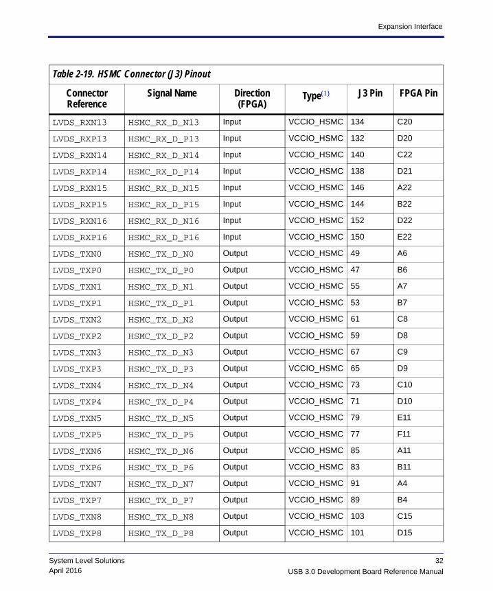
Expansion Interface
LVDS_RXN13 HSMC_RX_D_N13 Input VCCIO_HSMC 134 C20
LVDS_RXP13 HSMC_RX_D_P13 Input VCCIO_HSMC 132 D20
LVDS_RXN14 HSMC_RX_D_N14 Input VCCIO_HSMC 140 C22
LVDS_RXP14 HSMC_RX_D_P14 Input VCCIO_HSMC 138 D21
LVDS_RXN15 HSMC_RX_D_N15 Input VCCIO_HSMC 146 A22
LVDS_RXP15 HSMC_RX_D_P15 Input VCCIO_HSMC 144 B22
LVDS_RXN16 HSMC_RX_D_N16 Input VCCIO_HSMC 152 D22
LVDS_RXP16 HSMC_RX_D_P16 Input VCCIO_HSMC 150 E22
LVDS_TXN0 HSMC_TX_D_N0 Output VCCIO_HSMC 49 A6
LVDS_TXP0 HSMC_TX_D_P0 Output VCCIO_HSMC 47 B6
LVDS_TXN1 HSMC_TX_D_N1 Output VCCIO_HSMC 55 A7
LVDS_TXP1 HSMC_TX_D_P1 Output VCCIO_HSMC 53 B7
LVDS_TXN2 HSMC_TX_D_N2 Output VCCIO_HSMC 61 C8
LVDS_TXP2 HSMC_TX_D_P2 Output VCCIO_HSMC 59 D8
LVDS_TXN3 HSMC_TX_D_N3 Output VCCIO_HSMC 67 C9
LVDS_TXP3 HSMC_TX_D_P3 Output VCCIO_HSMC 65 D9
LVDS_TXN4 HSMC_TX_D_N4 Output VCCIO_HSMC 73 C10
LVDS_TXP4 HSMC_TX_D_P4 Output VCCIO_HSMC 71 D10
LVDS_TXN5 HSMC_TX_D_N5 Output VCCIO_HSMC 79 E11
LVDS_TXP5 HSMC_TX_D_P5 Output VCCIO_HSMC 77 F11
LVDS_TXN6 HSMC_TX_D_N6 Output VCCIO_HSMC 85 A11
LVDS_TXP6 HSMC_TX_D_P6 Output VCCIO_HSMC 83 B11
LVDS_TXN7 HSMC_TX_D_N7 Output VCCIO_HSMC 91 A4
LVDS_TXP7 HSMC_TX_D_P7 Output VCCIO_HSMC 89 B4
LVDS_TXN8 HSMC_TX_D_N8 Output VCCIO_HSMC 103 C15
LVDS_TXP8 HSMC_TX_D_P8 Output VCCIO_HSMC 101 D15
Table 2-19. HSMC Connector (J3) Pinout
Connector Reference
Signal Name Direction (FPGA)
Type(1) J3 Pin FPGA Pin
32
USB 3.0 Development Board Reference Manual
System Level SolutionsApril 2016
Expansion Interface
General Purpose I/O Headers (J6, J7)
There is a 6-pin headers (J6, J7) which can be used for general purpose I/O or
debugging.
LVDS_TXN9 HSMC_TX_D_N9 Output VCCIO_HSMC 109 C16
LVDS_TXP9 HSMC_TX_D_P9 Output VCCIO_HSMC 107 D16
LVDS_TXN10 HSMC_TX_D_N10 Output VCCIO_HSMC 115 C17
LVDS_TXP10 HSMC_TX_D_P10 Output VCCIO_HSMC 113 D17
LVDS_TXN11 HSMC_TX_D_N11 Output VCCIO_HSMC 121 A18
LVDS_TXP11 HSMC_TX_D_P11 Output VCCIO_HSMC 119 B18
LVDS_TXN12 HSMC_TX_D_N12 Output VCCIO_HSMC 127 E18
LVDS_TXP12 HSMC_TX_D_P12 Output VCCIO_HSMC 125 F18
LVDS_TXN13 HSMC_TX_D_N13 Output VCCIO_HSMC 133 C19
LVDS_TXP13 HSMC_TX_D_P13 Output VCCIO_HSMC 131 D19
LVDS_TXN14 HSMC_TX_D_N14 Output VCCIO_HSMC 139 A21
LVDS_TXP14 HSMC_TX_D_P14 Output VCCIO_HSMC 137 B21
LVDS_TXN15 HSMC_TX_D_N15 Output VCCIO_HSMC 145 E21
LVDS_TXP15 HSMC_TX_D_P15 Output VCCIO_HSMC 143 F21
LVDS_TXN16 HSMC_TX_D_N16 Output VCCIO_HSMC 151 A23
LVDS_TXP16 HSMC_TX_D_P16 Output VCCIO_HSMC 149 B23
Notes:
(1) For VCCIO_HSMC refer Table 2-26 .
Table 2-19. HSMC Connector (J3) Pinout
Connector Reference
Signal Name Direction (FPGA)
Type(1) J3 Pin FPGA Pin
33 System Level SolutionsApril 2016USB 3.0 Development Board Reference Manual
Clock Circuitry
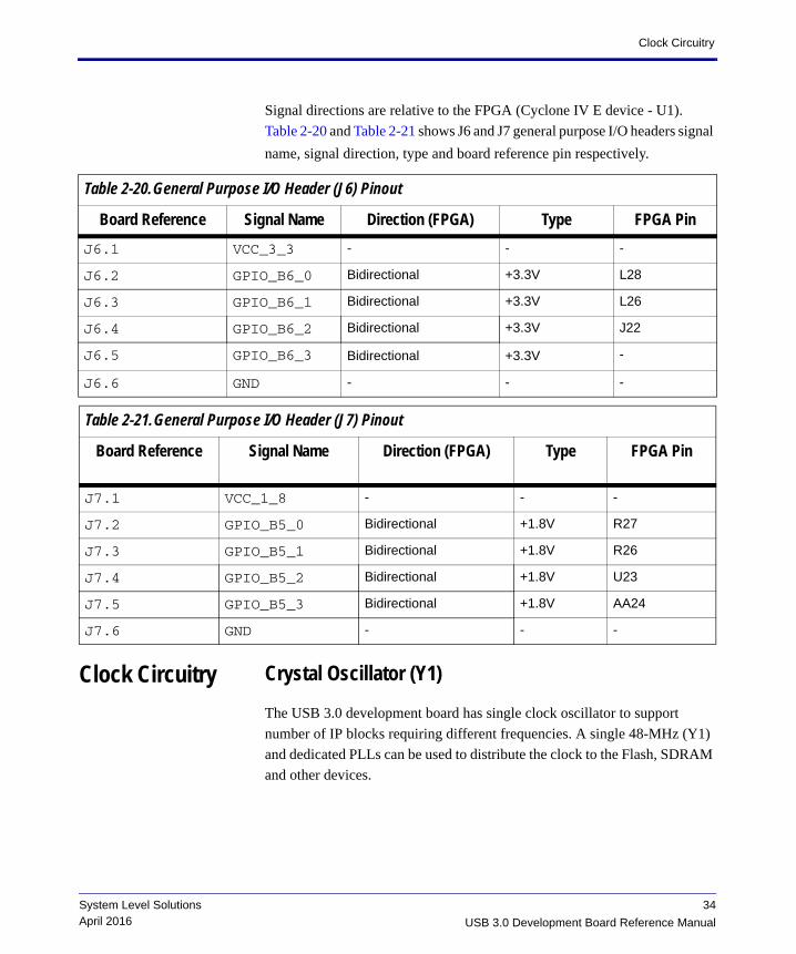
Signal directions are relative to the FPGA (Cyclone IV E device - U1). Table 2-20 and Table 2-21 shows J6 and J7 general purpose I/O headers signal
name, signal direction, type and board reference pin respectively.
Clock Circuitry Crystal Oscillator (Y1)
The USB 3.0 development board has single clock oscillator to support
number of IP blocks requiring different frequencies. A single 48-MHz (Y1)
and dedicated PLLs can be used to distribute the clock to the Flash, SDRAM
and other devices.
Table 2-20.General Purpose I/O Header (J6) Pinout
Board Reference Signal Name Direction (FPGA) Type FPGA Pin
J6.1 VCC_3_3 - - -
J6.2 GPIO_B6_0 Bidirectional +3.3V L28
J6.3 GPIO_B6_1 Bidirectional +3.3V L26
J6.4 GPIO_B6_2 Bidirectional +3.3V J22
J6.5 GPIO_B6_3 Bidirectional +3.3V -
J6.6 GND - - -
Table 2-21.General Purpose I/O Header (J7) Pinout
Board Reference Signal Name Direction (FPGA) Type FPGA Pin
J7.1 VCC_1_8 - - -
J7.2 GPIO_B5_0 Bidirectional +1.8V R27
J7.3 GPIO_B5_1 Bidirectional +1.8V R26
J7.4 GPIO_B5_2 Bidirectional +1.8V U23
J7.5 GPIO_B5_3 Bidirectional +1.8V AA24
J7.6 GND - - -
34
USB 3.0 Development Board Reference Manual
System Level SolutionsApril 2016
Power Supply
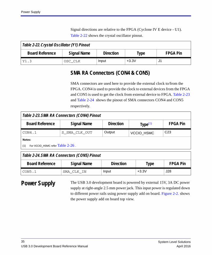
Signal directions are relative to the FPGA (Cyclone IV E device - U1). Table 2-22 shows the crystal oscillator pinout.
SMA RA Connectors (CON4 & CON5)
SMA connectors are used here to provide the external clock to/from the
FPGA. CON4 is used to provide the clock to external devices from the FPGA
and CON5 is used to get the clock from external device to FPGA. Table 2-23
and Table 2-24 shows the pinout of SMA connectors CON4 and CON5
respectively.
Power Supply The USB 3.0 development board is powered by external 15V, 3A DC power
supply at right-angle 2.5 mm power jack. This input power is regulated down
to different power rails using power supply add on board. Figure 2-2. shows
the power supply add on board top view.
Table 2-22.Crystal Oscillator (Y1) Pinout
Board Reference Signal Name Direction Type FPGA Pin
Y1.3 OSC_CLK Input +3.3V J1
Table 2-23.SMA RA Connectors (CON4) Pinout
Board Reference Signal Name Direction Type(1) FPGA Pin
CON4.1 S_SMA_CLK_OUT Output VCCIO_HSMC C23
Notes:
(1) For VCCIO_HSMC refer Table 2-26 .
Table 2-24.SMA RA Connectors (CON5) Pinout
Board Reference Signal Name Direction Type FPGA Pin
CON5.1 SMA_CLK_IN Input +3.3V J28
35 System Level SolutionsApril 2016USB 3.0 Development Board Reference Manual
Power Supply
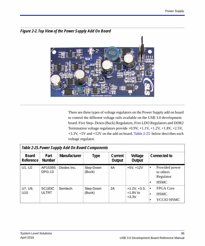
Figure 2-2. Top View of the Power Supply Add On Board
There are three types of voltage regulators on the Power Supply add on board
to control the different voltage rails available on the USB 3.0 development
board. Five Step- Down (Buck) Regulators, Five LDO Regulators and DDR2
Termination voltage regulators provide +0.9V, +1.1V, +1.2V, +1.8V, +2.5V,
+3.3V, +5V and +12V on the add on board. Table 2-25 below describes each
voltage regulator.
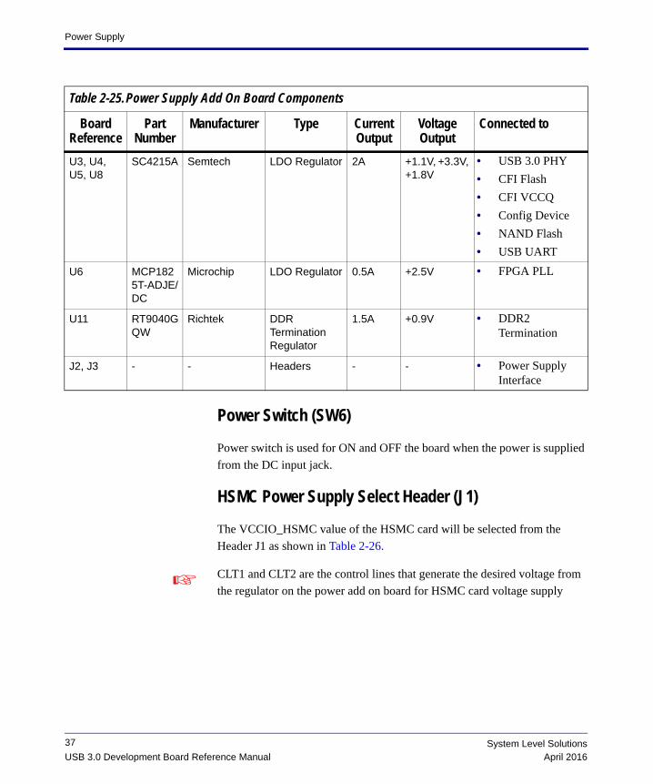
Table 2-25.Power Supply Add On Board Components
Board Reference
Part Number
Manufacturer Type Current Output
Voltage Output
Connected to
U1, U2 AP1539SDPG-13
Diodes Inc, Step-Down (Buck)
4A +5V, +12V • Provided power to others Regulator
• HSMC
U7, U9, U10
SC183CULTRT
Semtech Step-Down (Buck)
2A +1.2V, +3.3, +1.8V to +3.3V
• FPGA Core
• HSMC
• VCCIO HSMC
36
USB 3.0 Development Board Reference Manual
System Level SolutionsApril 2016
Power Supply
Power Switch (SW6)
Power switch is used for ON and OFF the board when the power is supplied
from the DC input jack.
HSMC Power Supply Select Header (J1)
The VCCIO_HSMC value of the HSMC card will be selected from the
Header J1 as shown in Table 2-26.
CLT1 and CLT2 are the control lines that generate the desired voltage from
the regulator on the power add on board for HSMC card voltage supply
U3, U4, U5, U8
SC4215A Semtech LDO Regulator 2A +1.1V, +3.3V, +1.8V
• USB 3.0 PHY
• CFI Flash
• CFI VCCQ
• Config Device
• NAND Flash
• USB UART
U6 MCP1825T-ADJE/DC
Microchip LDO Regulator 0.5A +2.5V • FPGA PLL
U11 RT9040GQW
Richtek DDR Termination Regulator
1.5A +0.9V • DDR2 Termination
J2, J3 - - Headers - - • Power Supply Interface
Table 2-25.Power Supply Add On Board Components
Board Reference
Part Number
Manufacturer Type Current Output
Voltage Output
Connected to
37 System Level SolutionsApril 2016USB 3.0 Development Board Reference Manual
Power Supply
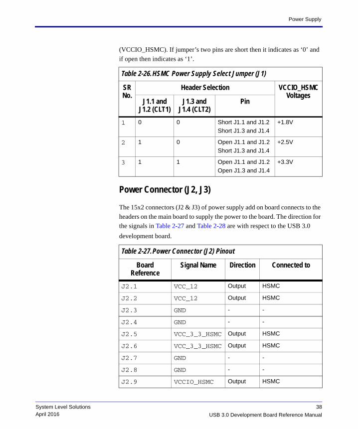
(VCCIO_HSMC). If jumper’s two pins are short then it indicates as ‘0’ and
if open then indicates as ‘1’.
Power Connector (J2, J3)
The 15x2 connectors (J2 & J3) of power supply add on board connects to the
headers on the main board to supply the power to the board. The direction for
the signals in Table 2-27 and Table 2-28 are with respect to the USB 3.0
development board.
Table 2-26.HSMC Power Supply Select Jumper (J1)
SR No.
Header Selection VCCIO_HSMC Voltages
J1.1 and J1.2 (CLT1)
J1.3 and J1.4 (CLT2)
Pin
1 0 0 Short J1.1 and J1.2
Short J1.3 and J1.4
+1.8V
2 1 0 Open J1.1 and J1.2
Short J1.3 and J1.4
+2.5V
3 1 1 Open J1.1 and J1.2
Open J1.3 and J1.4
+3.3V
Table 2-27.Power Connector (J2) Pinout
Board Reference
Signal Name Direction Connected to
J2.1 VCC_12 Output HSMC
J2.2 VCC_12 Output HSMC
J2.3 GND - -
J2.4 GND - -
J2.5 VCC_3_3_HSMC Output HSMC
J2.6 VCC_3_3_HSMC Output HSMC
J2.7 GND - -
J2.8 GND - -
J2.9 VCCIO_HSMC Output HSMC
38
USB 3.0 Development Board Reference Manual
System Level SolutionsApril 2016
Power Supply
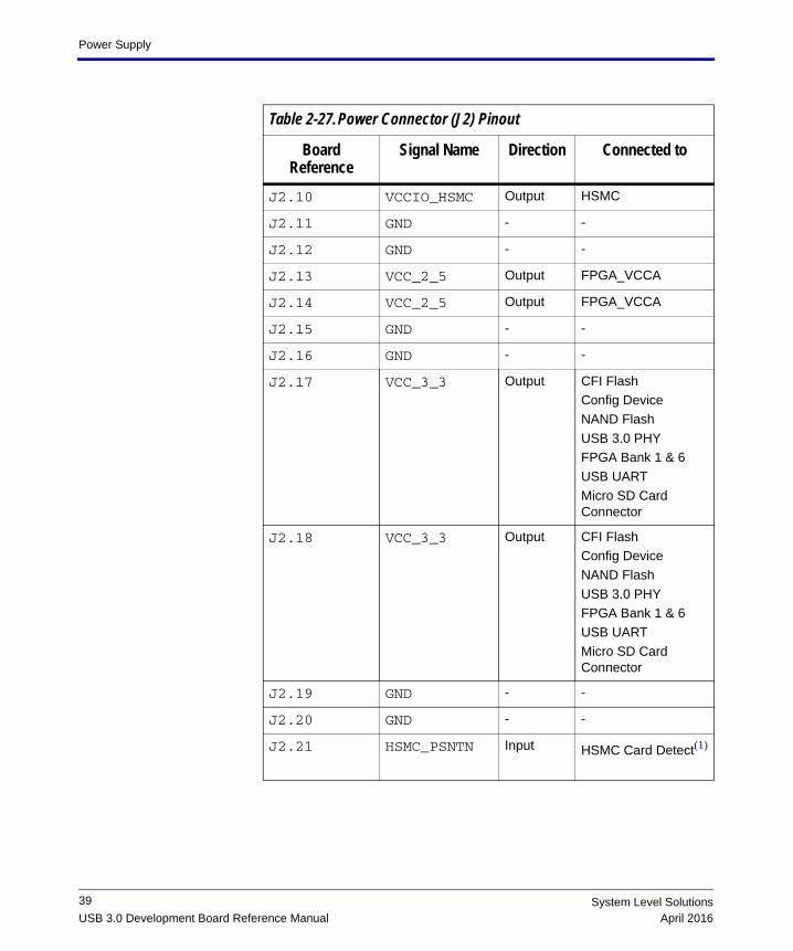
J2.10 VCCIO_HSMC Output HSMC
J2.11 GND - -
J2.12 GND - -
J2.13 VCC_2_5 Output FPGA_VCCA
J2.14 VCC_2_5 Output FPGA_VCCA
J2.15 GND - -
J2.16 GND - -
J2.17 VCC_3_3 Output CFI Flash
Config Device
NAND Flash
USB 3.0 PHY
FPGA Bank 1 & 6
USB UART
Micro SD Card Connector
J2.18 VCC_3_3 Output CFI Flash
Config Device
NAND Flash
USB 3.0 PHY
FPGA Bank 1 & 6
USB UART
Micro SD Card Connector
J2.19 GND - -
J2.20 GND - -
J2.21 HSMC_PSNTN Input HSMC Card Detect(1)
Table 2-27.Power Connector (J2) Pinout
Board Reference
Signal Name Direction Connected to
39 System Level SolutionsApril 2016USB 3.0 Development Board Reference Manual
Power Supply
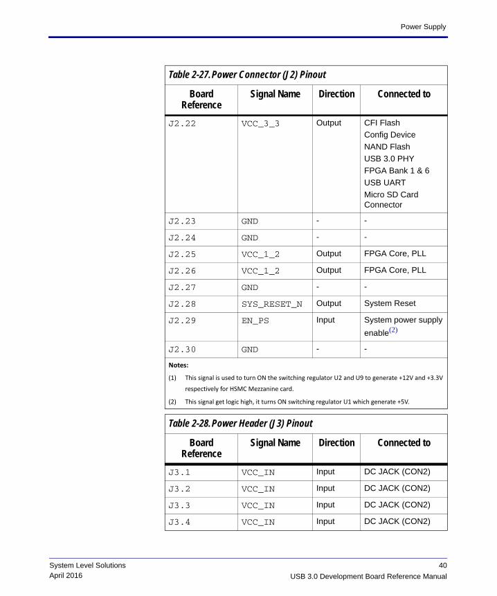
J2.22 VCC_3_3 Output CFI Flash
Config Device
NAND Flash
USB 3.0 PHY
FPGA Bank 1 & 6
USB UART
Micro SD Card Connector
J2.23 GND - -
J2.24 GND - -
J2.25 VCC_1_2 Output FPGA Core, PLL
J2.26 VCC_1_2 Output FPGA Core, PLL
J2.27 GND - -
J2.28 SYS_RESET_N Output System Reset
J2.29 EN_PS Input System power supply
enable(2)
J2.30 GND - -
Notes:
(1) This signal is used to turn ON the switching regulator U2 and U9 to generate +12V and +3.3V
respectively for HSMC Mezzanine card.
(2) This signal get logic high, it turns ON switching regulator U1 which generate +5V.
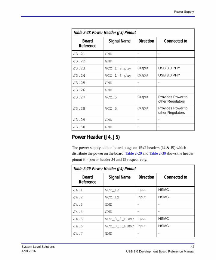
Table 2-28.Power Header (J3) Pinout
Board Reference
Signal Name Direction Connected to
J3.1 VCC_IN Input DC JACK (CON2)
J3.2 VCC_IN Input DC JACK (CON2)
J3.3 VCC_IN Input DC JACK (CON2)
J3.4 VCC_IN Input DC JACK (CON2)
Table 2-27.Power Connector (J2) Pinout
Board Reference
Signal Name Direction Connected to
40
USB 3.0 Development Board Reference Manual
System Level SolutionsApril 2016
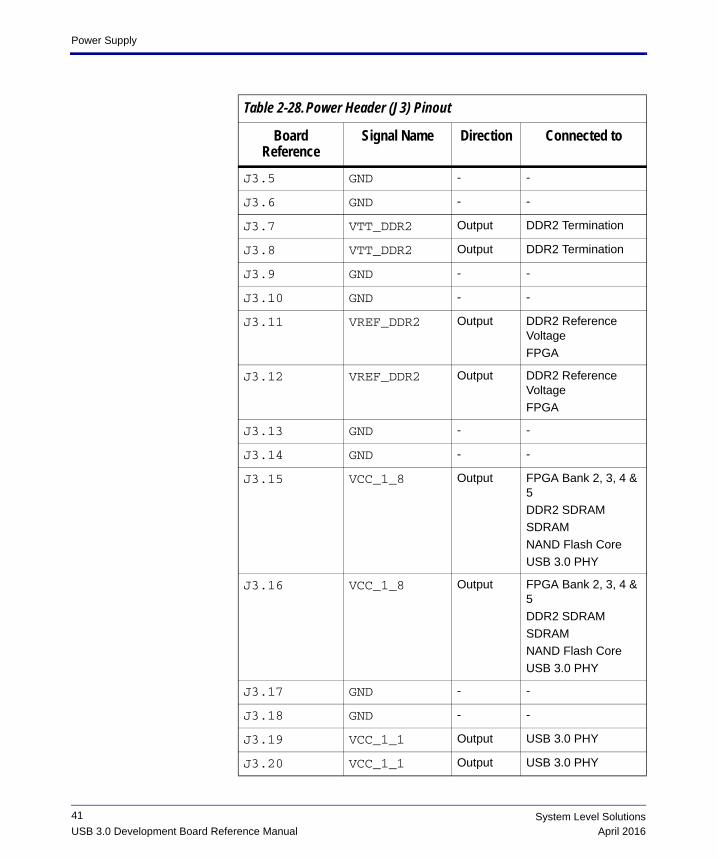
Power Supply
J3.5 GND - -
J3.6 GND - -
J3.7 VTT_DDR2 Output DDR2 Termination
J3.8 VTT_DDR2 Output DDR2 Termination
J3.9 GND - -
J3.10 GND - -
J3.11 VREF_DDR2 Output DDR2 Reference Voltage
FPGA
J3.12 VREF_DDR2 Output DDR2 Reference Voltage
FPGA
J3.13 GND - -
J3.14 GND - -
J3.15 VCC_1_8 Output FPGA Bank 2, 3, 4 & 5
DDR2 SDRAM
SDRAM
NAND Flash Core
USB 3.0 PHY
J3.16 VCC_1_8 Output FPGA Bank 2, 3, 4 & 5
DDR2 SDRAM
SDRAM
NAND Flash Core
USB 3.0 PHY
J3.17 GND - -
J3.18 GND - -
J3.19 VCC_1_1 Output USB 3.0 PHY
J3.20 VCC_1_1 Output USB 3.0 PHY
Table 2-28.Power Header (J3) Pinout
Board Reference
Signal Name Direction Connected to
41 System Level SolutionsApril 2016USB 3.0 Development Board Reference Manual
Power Supply
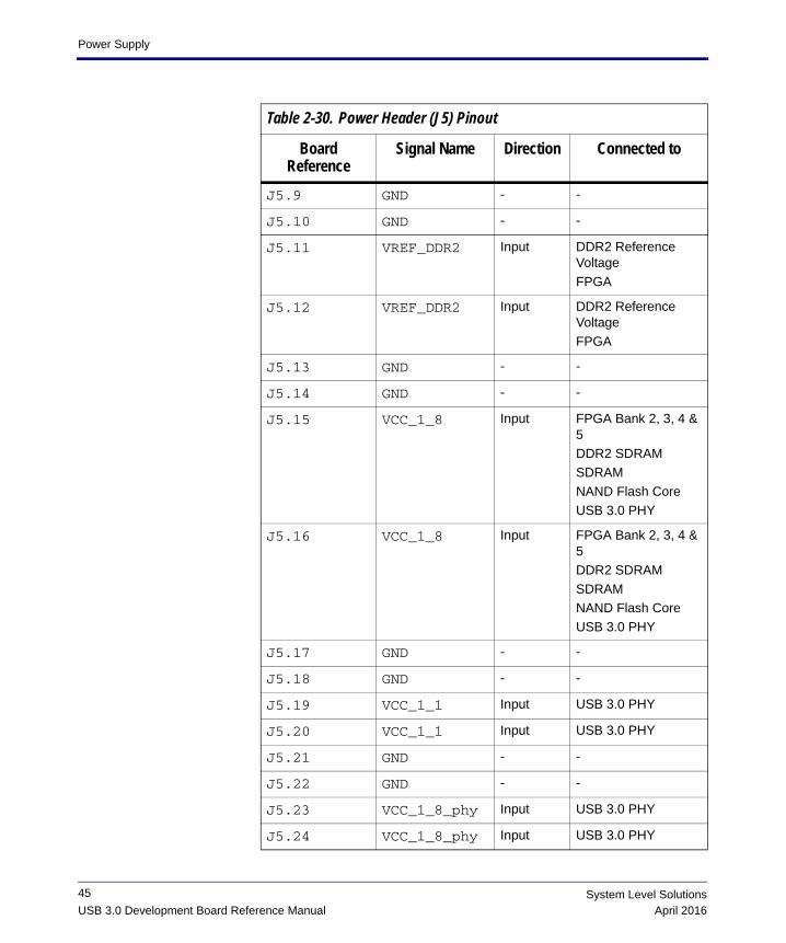
Power Header (J4, J5)
The power supply add on board plugs on 15x2 headers (J4 & J5) which
distribute the power on the board. Table 2-29 and Table 2-30 shows the header
pinout for power header J4 and J5 respectively.
J3.21 GND - -
J3.22 GND - -
J3.23 VCC_1_8_phy Output USB 3.0 PHY
J3.24 VCC_1_8_phy Output USB 3.0 PHY
J3.25 GND - -
J3.26 GND - -
J3.27 VCC_5 Output Provides Power to other Regulators
J3.28 VCC_5 Output Provides Power to other Regulators
J3.29 GND - -
J3.30 GND - -
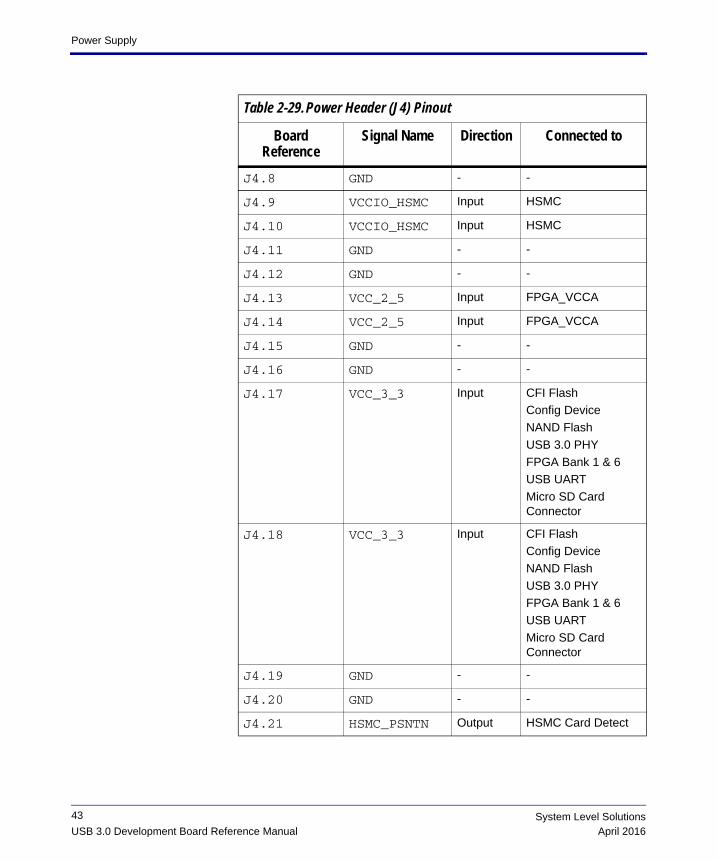
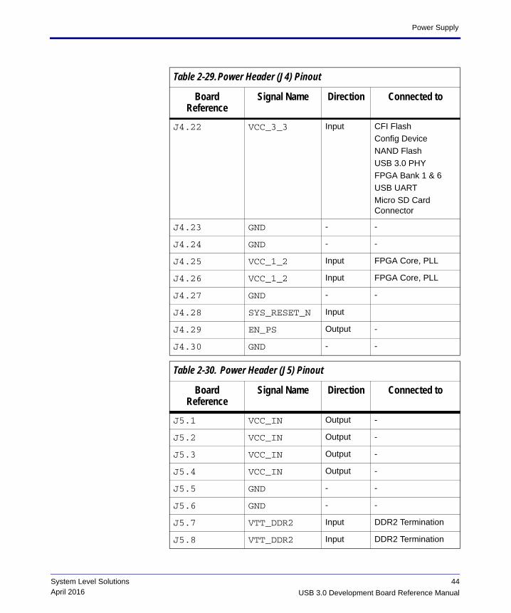
Table 2-29.Power Header (J4) Pinout
Board Reference
Signal Name Direction Connected to
J4.1 VCC_12 Input HSMC
J4.2 VCC_12 Input HSMC
J4.3 GND - -
J4.4 GND - -
J4.5 VCC_3_3_HSMC Input HSMC
J4.6 VCC_3_3_HSMC Input HSMC
J4.7 GND - -
Table 2-28.Power Header (J3) Pinout
Board Reference
Signal Name Direction Connected to
42
USB 3.0 Development Board Reference Manual
System Level SolutionsApril 2016
Power Supply
J4.8 GND - -
J4.9 VCCIO_HSMC Input HSMC
J4.10 VCCIO_HSMC Input HSMC
J4.11 GND - -
J4.12 GND - -
J4.13 VCC_2_5 Input FPGA_VCCA
J4.14 VCC_2_5 Input FPGA_VCCA
J4.15 GND - -
J4.16 GND - -
J4.17 VCC_3_3 Input CFI Flash
Config Device
NAND Flash
USB 3.0 PHY
FPGA Bank 1 & 6
USB UART
Micro SD Card Connector
J4.18 VCC_3_3 Input CFI Flash
Config Device
NAND Flash
USB 3.0 PHY
FPGA Bank 1 & 6
USB UART
Micro SD Card Connector
J4.19 GND - -
J4.20 GND - -
J4.21 HSMC_PSNTN Output HSMC Card Detect
Table 2-29.Power Header (J4) Pinout
Board Reference
Signal Name Direction Connected to
43 System Level SolutionsApril 2016USB 3.0 Development Board Reference Manual
Power Supply
J4.22 VCC_3_3 Input CFI Flash
Config Device
NAND Flash
USB 3.0 PHY
FPGA Bank 1 & 6
USB UART
Micro SD Card Connector
J4.23 GND - -
J4.24 GND - -
J4.25 VCC_1_2 Input FPGA Core, PLL
J4.26 VCC_1_2 Input FPGA Core, PLL
J4.27 GND - -
J4.28 SYS_RESET_N Input
J4.29 EN_PS Output -
J4.30 GND - -
Table 2-30. Power Header (J5) Pinout
Board Reference
Signal Name Direction Connected to
J5.1 VCC_IN Output -
J5.2 VCC_IN Output -
J5.3 VCC_IN Output -
J5.4 VCC_IN Output -
J5.5 GND - -
J5.6 GND - -
J5.7 VTT_DDR2 Input DDR2 Termination
J5.8 VTT_DDR2 Input DDR2 Termination
Table 2-29.Power Header (J4) Pinout
Board Reference
Signal Name Direction Connected to
44
USB 3.0 Development Board Reference Manual
System Level SolutionsApril 2016
Power Supply
J5.9 GND - -
J5.10 GND - -
J5.11 VREF_DDR2 Input DDR2 Reference Voltage
FPGA
J5.12 VREF_DDR2 Input DDR2 Reference Voltage
FPGA
J5.13 GND - -
J5.14 GND - -
J5.15 VCC_1_8 Input FPGA Bank 2, 3, 4 & 5
DDR2 SDRAM
SDRAM
NAND Flash Core
USB 3.0 PHY
J5.16 VCC_1_8 Input FPGA Bank 2, 3, 4 & 5
DDR2 SDRAM
SDRAM
NAND Flash Core
USB 3.0 PHY
J5.17 GND - -
J5.18 GND - -
J5.19 VCC_1_1 Input USB 3.0 PHY
J5.20 VCC_1_1 Input USB 3.0 PHY
J5.21 GND - -
J5.22 GND - -
J5.23 VCC_1_8_phy Input USB 3.0 PHY
J5.24 VCC_1_8_phy Input USB 3.0 PHY
Table 2-30. Power Header (J5) Pinout
Board Reference
Signal Name Direction Connected to
45 System Level SolutionsApril 2016USB 3.0 Development Board Reference Manual
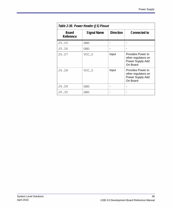
Power Supply
J5.25 GND - -
J5.26 GND - -
J5.27 VCC_5 Input Provides Power to other regulators on Power Supply Add On Board
J5.28 VCC_5 Input Provides Power to other regulators on Power Supply Add On Board
J5.29 GND - -
J5.30 GND - -
Table 2-30. Power Header (J5) Pinout
Board Reference
Signal Name Direction Connected to
46
USB 3.0 Development Board Reference Manual
System Level SolutionsApril 2016