US000008784766B120140722 - ntrs.nasa.gov · Raman Shift (cm-1) (b) D band ~ N C c Diamond ... lium...
10
1111111111111111111111111111111111111111111111111111111111111111111111111111 (12) United States Patent Uppireddi et al. (54) DIAMOND SYNTHESIS EMPLOYING NANOPARTICLE SEEDS (75) Inventors: Kishore Uppireddi, San Juan, PR (US); Gerardo Morell, Guaynabo, PR (US); Brad R. Weiner, Dorado, PR (US) (73) Assignee: The University of Puerto Rico, San Juan, PR (US) (*) Notice: Subject to any disclaimer, the term of this patent is extended or adjusted under 35 U.S.C. 154(b) by 318 days. (21) Appl. No.: 12/689,180 (22) Filed: Jan. 18, 2010 Related U.S. Application Data (60) Provisional application No. 61/145,260, filed on Jan 16, 2009. (51) Int. Cl. BOIJ3106 (2006.01) (52) U.S. Cl. USPC ........................................... 423/446; 977/773 (58) Field of Classification Search None See application file for complete search history. (56) References Cited U.S. PATENT DOCUMENTS 4,254,091 A * 3/1981 Woermann et al............ 423/446 5,264,701 A * 11/1993 Crain ............................ 250/374 5,437,891 A * 8/1995 Anthony et al. ......... 427/249.11 (lo) Patent No.: US 8,784,766 B1 (45) Date of Patent: Jul. 22 9 2014 5,485,804 A * 1/1996 Adair et al . ..................... 117/90 6,001,304 A * 12/1999 Yooetal ......................... 419/10 2008/0187479 Al * 8/2008 Munday ........................ 423/290 2009/0257942 Al * 10/2009 Sung ............................. 423/446 OTHER PUBLICATIONS Machi et al. Synthesis of Diamond Using Fe Catalysts by RF Plasma Chemical Vapor Deposition Method; Jpn. J. Appl. Phys.; vol. 31 pp. 1958-1963; 1992.* Resto et al.; Iron Oxide Nanoparticles Employed as Seeds for the Induction of Microcrystalline Diamond Synthesis; Nanoscale Re. Lett. 3, pp. 65-70; Jan. 24, 2008.* Haubner et al.; Sol-gel preparation of Catalyst Particles on Substrates for Hot-Filament CVD Nanotube Deposition; Diamond & Related Materials; 17, pp. 1452-1457; 2008.* Machi et al.; Synthesis of Diamond Using Fe Catalysts by RF Plasma Chemical Vapor Deposition Method; Jpn. J. Appl. Phys.; vol. 31 pp. 1958-1963; 1992.* * cited by examiner Primary Examiner Guinever Gregorio (74) Attorney, Agent, or Firm Hoglund & Pamias, P.S.C.; Roberto J. Rios (57) ABSTRACT Iron nanoparticles were employed to induce the synthesis of diamond on molybdenum, silicon, and quartz substrates. Dia- mond films were grown using conventional conditions for diamond synthesis by hot filament chemical vapor deposi- tion, except that dispersed iron oxide nanoparticles replaced the seeding. This approach to diamond induction can be com- bined with dip pen nanolithography for the selective deposi- tion of diamond and diamond patterning while avoiding sur- face damage associated to diamond-seeding methods. 27 Claims, 5 Drawing Sheets https://ntrs.nasa.gov/search.jsp?R=20150003331 2018-08-19T22:53:37+00:00Z
Transcript of US000008784766B120140722 - ntrs.nasa.gov · Raman Shift (cm-1) (b) D band ~ N C c Diamond ... lium...

1111111111111111111111111111111111111111111111111111111111111111111111111111
(12) United States Patent Uppireddi et al.
(54) DIAMOND SYNTHESIS EMPLOYING NANOPARTICLE SEEDS
(75) Inventors: Kishore Uppireddi, San Juan, PR (US); Gerardo Morell, Guaynabo, PR (US); Brad R. Weiner, Dorado, PR (US)
(73) Assignee: The University of Puerto Rico, San Juan, PR (US)
(*) Notice: Subject to any disclaimer, the term of this patent is extended or adjusted under 35 U.S.C. 154(b) by 318 days.
(21) Appl. No.: 12/689,180
(22) Filed: Jan. 18, 2010
Related U.S. Application Data
(60) Provisional application No. 61/145,260, filed on Jan 16, 2009.
(51) Int. Cl. BOIJ3106 (2006.01)
(52) U.S. Cl. USPC ........................................... 423/446; 977/773
(58) Field of Classification Search None See application file for complete search history.
(56) References Cited
U.S. PATENT DOCUMENTS
4,254,091 A * 3/1981 Woermann et al............ 423/446 5,264,701 A * 11/1993 Crain ............................ 250/374 5,437,891 A * 8/1995 Anthony et al. ......... 427/249.11
(lo) Patent No.: US 8,784,766 B1 (45) Date of Patent: Jul. 22 9 2014
5,485,804 A * 1/1996 Adair et al . ..................... 117/90 6,001,304 A * 12/1999 Yooetal ......................... 419/10
2008/0187479 Al * 8/2008 Munday ........................ 423/290 2009/0257942 Al * 10/2009 Sung ............................. 423/446
OTHER PUBLICATIONS
Machi et al. Synthesis of Diamond Using Fe Catalysts by RF Plasma
Chemical Vapor Deposition Method; Jpn. J. Appl. Phys.; vol. 31 pp.
1958-1963; 1992.* Resto et al.; Iron Oxide Nanoparticles Employed as Seeds for the Induction of Microcrystalline Diamond Synthesis; Nanoscale Re. Lett. 3, pp. 65-70; Jan. 24, 2008.* Haubner et al.; Sol-gel preparation of Catalyst Particles on Substrates for Hot-Filament CVD Nanotube Deposition; Diamond & Related Materials; 17, pp. 1452-1457; 2008.* Machi et al.; Synthesis of Diamond Using Fe Catalysts by RF Plasma Chemical Vapor Deposition Method; Jpn. J. Appl. Phys.; vol. 31 pp. 1958-1963; 1992.*
* cited by examiner
Primary Examiner Guinever Gregorio (74) Attorney, Agent, or Firm Hoglund & Pamias, P.S.C.; Roberto J. Rios
(57) ABSTRACT
Iron nanoparticles were employed to induce the synthesis of diamond on molybdenum, silicon, and quartz substrates. Dia-mond films were grown using conventional conditions for diamond synthesis by hot filament chemical vapor deposi-tion, except that dispersed iron oxide nanoparticles replaced the seeding. This approach to diamond induction can be com-bined with dip pen nanolithography for the selective deposi-tion of diamond and diamond patterning while avoiding sur-face damage associated to diamond-seeding methods.
27 Claims, 5 Drawing Sheets
https://ntrs.nasa.gov/search.jsp?R=20150003331 2018-08-19T22:53:37+00:00Z
U.S. Patent Jul. 22 9 2014 Sheet 1 of 5 US 8,784,766 B1
c~
m c
40 50 60 70 80 90 100
Meta
FIG.2
U.S. Patent Jul. 22 9 2014 Sheet 2 of 5 US 8,784,766 B1
M
V LL

U.S. Patent Jul. 22 9 2014 Sheet 3 of 5 US 8,784,766 B1
(a)
N C
C
Visible
FIG. 4
UV_
1200 1300 1400 1500 1600 1700 Raman Shift (cm -1 )
(b)
D band
~N C
c Diamond pea
1200 1300 1400 1500 Raman Shift (cm -1 )
~G band
1600 1700
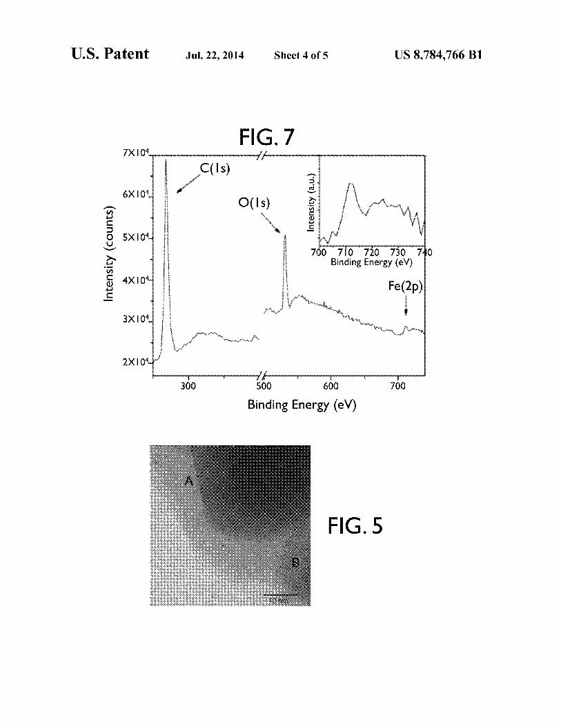
FIG.7
300 500
600 700
Binding Energy (eV)
FIG.5
5)
,P3
N
N
7X1
6X1
4j
O 5X1 v
4X1 4j
3X1
2X1
710 720 730 7 Binding Energy (eV)
Fe(2p)
i
U.S. Patent Jul. 22 9 2014 Sheet 4 of 5
US 8,784,766 B1

FIG.6
(b)
a~
J
U.S. Patent Jul. 22 9 2014 Sheet 5 of 5 US 8 ,784,766 B1
Energy Loss (eV)
US 8,784,766 B1
DIAMOND SYNTHESIS EMPLOYING NANOPARTICLE SEEDS
GOVERNMENT INTEREST
The claimed invention was made with U.S. Government support under grant number NSF-0701525 awarded by the National Science Foundation (NSF), and grant numbers NNG05GG78H, NCC5-595 and NCC3-1034 awarded by the National Aeronautics and Space Administration (NASA). The government has certain rights in this invention.
BACKGROUND OF THE INVENTION
Many challenges remain opening regarding the integration of diamond into electronic devices. In particular, seeding processes are typically harsh on the substrate surface, leading to defect creation and lack of reproducibility. Iron-based materials have been used as catalysts in the synthesis of crystalline diamond by high temperature, high-pressure growth. Yet, it is difficult to fabricate diamond on iron-based materials by chemical vapor deposition (CVD) due to the rapid diffusion of carbon into the bulk and high carbon solu-bility. There have been a number of attempts to grow diamond by forming a thin film of iron on silicon substrates. Higher diamond nucleation densities with significant amounts of a-C are attained by depositing a thin layer of iron on silicon substrates, thus suggesting that a high carbon concentration resulting in a saturated carbide layer during the initial stage of nucleation is required for producing diamond nucleation sites. The prior art further indicates that there is an optimum iron thickness at which diamond growth prevails.
Thus, there exists a need for an efficient process that selec-tively yields high quality diamond films at relatively high growth rate with negligible co-deposition of amorphous car-bon, and avoids any pre and post treatment of the substrate in order to prevent any undue damage to it.
SUMMARY OF THE INVENTION
The above-described developments suggest that the Fe nanoparticles can be employed as diamond nucleation cen-ters: they have a strong affinity for C atoms and yet they are too small to act as C sinks. FeO nanoparticles (nFeO) are ideal candidates for this task because the Fe nanoparticle is passi-vated by O, which is then removed by the CVD reactions, leaving the active Fe nanoparticle exposed for C trapping and accumulation.
The present invention provides an efficient process of pro-ducing high quality diamond films on metal, semiconductor or insulator substrates, employing metal compound nanopar-ticle seeds.
According to an aspect of the invention, diamond is obtained over a substrate is by providing a substrate; depos-iting metal compound nanoparticle seeds on the substrate, said metal being capable of carbide formation; and directing a stream of fluid composition at the seeded substrate under conditions that effect diamond growth.
In accordance to another aspect of the invention, a metal substrate is selected from copper, molybdenum, aluminum, tantalum, tungsten, nickel or combinations thereof.
According to a further aspect of the invention, the semi-conductor substrate is selected from silicon, germanium, gal-lium arsenide or combinations thereof.
In still another aspect of the invention, the insulator sub-strate is selected from quartz, glass, gallium nitride, silicon carbide, boron nitride or combinations thereof.
2 The present invention particularly provides a process for
selective deposition of diamond on silicon, molybdenum or quartz substrate using Iron oxide nanoparticles (nFeO) as seeds. One important aspect of the present invention is that
5 the process is devoid of any diamond powder seeding and avoids subjecting the substrate to any undue damage.
In an aspect of the invention, the metal compound nano-particles of this invention are characterized by a size in the range of 1-50 mu, preferably 4-15 mu.
io In another aspect of invention, the metal compound nano-particles of this invention are characterized by a surface den-sity in the range of 10 5 -10 10 per cm2 , preferably 10'-10 10 per cm2 .
The distribution of nanoparticles plays a significant role in 15 the deposition of diamond film on the substrate. Thus, accord-
ing to an aspect of the invention the process provides a nano-particle layer that is uniformly distributed.
According to another aspect of the invention, the coated substrates of the present process are kept at a temperature in
20 a range of from about 100° C. to about 1000° C., preferably in a range of from 400° C. to 800° C.
In the process of the present invention no post-treatment like plasma etching is required to enhance thepost-deposition quality of the diamond films. Thus, in a further aspect of the
25 invention, a process is provided wherein the growth rate for diamond formation is in the range of 1.7-1.9 µm/h.
According to an aspect of the invention, a fluid composi-tion is directed on the substrate seeded with metal nanopar-ticles, and said composition comprises at least one compound
3o having at least one carbon-hydrogen bond and a diluent gas. In an embodiment of the invention the compound having at least one carbon-hydrogen bond is methane. According to another embodiment of the present invention the diluent gas is selected from hydrogen, nitrogen, helium, neon, argon,
35 xenon or krypton. In another aspect of the invention, the process of obtaining
diamond over a substrate comprises providing a substrate; depositing iron oxide nanoparticles seeds on the substrate; and directing a stream of carbon-containing fluid composi-
40 tion at the seeded substrate under conditions that effect dia-mond growth.
In a further aspect of the invention, the coated substrate is kept at a temperature in a range of from about 700° C. to about 750° C. and the fluid composition comprises methane (CH 4)
45 and hydrogen (H2). The iron oxide nanoparticles used to induce the formation of microcrystalline diamond films have a uniform size distribution in the range of 7-10 nm and a surface density in the range of 10'-10 10 per cm2 .
The observed diamond nucleation density was of the same 50 value as the initial nFeO surface density and was similar to
those typically obtained by diamond-seeded deposition pro-cess. This result is contrary to the prior art methods that involved some form of Fe seeding (typically thin Fe films) but suffered from substantial co-deposition of amorphous car-
55 bon. According to another aspect of the invention, the process
can be used for selective diamond deposition and patterning at the nanoscale level through Dip Pen Nanolithography fol-lowed by chemical vapor deposition and can be applied to
60 coat high quality crystalline diamond to structures with high aspect ratio, the interior surfaces of odd shaped structures and conformal coating on cutting tools with ease by adopting a convenient method of placing the FeO nanoparticles uni-formly.
65 The extreme properties of diamond (i.e., large electrical breakdown field, high saturated current density, high thermal conductivity) lead to the applicability of diamond to high

US 8,784,766 B1 3
temperature and high power devices. The present invention is a novel diamond process technology with minimum defect creation that does not impede the carriers mobility, and is an efficient process for producing high quality diamond for the potential integration of diamond into active electronic appli-cation. The selectivity of the deposition process renders added advantage to the device manufacturing with the current silicon microelectronic processing technologies.
According to a further aspect of the invention, the process can also be used to provide protective coating for metal and non-metal substrates to avoid their wear and tear especially in the field of prosthetics, tribology and microelectronics.
BRIEF DESCRIPTION OF THE DRAWINGS
Further features and advantages of the invention will become apparent from the following detailed description taken in conjunction with the accompanying figures showing illustrative embodiments of the invention, in which:
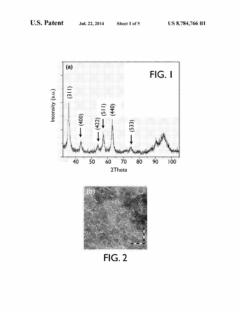
FIG. 1 shows an X-ray diffractogram of nFeO particles employed to induce diamond growth according to an embodi-ment of the present invention.
FIG. 2 is an EFTEM image of nFeO showing its particle size according to an embodiment of the present invention.
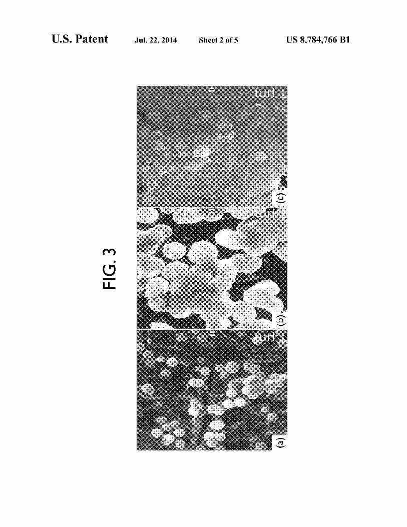
FIG. 3 shows SEM images of nFeO-induced diamond deposited on Mo substrates for (a) 30 min, (b) 2 h and (c) 6 h according to an embodiment of the present invention.
FIG. 4 shows a plot of representative visible and UV Raman spectra of nFeO-induced microcrystalline diamond on Mo substrates and a plot of deconvoluted visible Raman spectrum according to an embodiment of the present inven-tion.
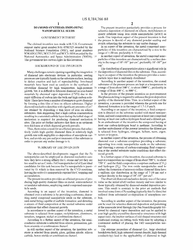
FIG. 5 is an EFTEM image showing the aggregation of carbon material around the Fe nanoparticle area according to an embodiment of the present invention.
FIG. 6 shows comparison spectra for nFeO, a-C, and dia-mond according to an embodiment of the present invention.
FIG. 7 shows carbon is core spectrum according to an embodiment of the present invention.
DETAILED DESCRIPTION OF THE INVENTION
Experimental Details A seed solution of iron oxide nanoparticle was prepared by
dissolving 2-4 g of iron oxide nanoparticle (nFeO) powder in 30 ml of methanol. The solution was then ultrasonicated from about 15-20 min. Microcrystalline diamond particles and films were synthesized using a custom-built hot filament CVD (HFCVD) apparatus. The films were grown on 14-mm diameter and 0.5-mm thick Mo, Si, and quartz substrates. The substrates were cleaned by sonication in methanol and acetone and dried with inert gas. The nanoparticle seed solu-tion was coated on the substrate using a spin coater for uni-form distribution of nFeO particles on the substrate, which is vital for obtaining a uniform diamond film. After cleaning, a suspension of nFeO with nominal particle size distribution in the 7-10 nun range was applied to the substrates. The surface density of nFeO clusters was estimated to be -10' CM
-2 by
atomic force microscopy and scanning electron microscopy (SEM). However, scattered micron-size patches of unseeded substrate remained. No diamond powder seeding was employed.
A mixture of 2% CH4 in H2 with a total flow of 100 sccm was directed over the heated rhenium filament kept at 2,700 K and 10 mm above the substrate. The total pressure was kept constant at values between 20 and 50 Torr (2.6-6.6 kPa). The
4 substrates were maintained around 700-730° C. and the depo-sition time was varied between 30 min and 6 h.
The surface morphology of the films was investigated by SEM. Small portions of the diamond samples were placed on
5 Formvar-coated Cu grids and uncoated silicon nitride TEM grids for energy-filtered transmission electron microscopy (EFTEM) and electron energy-loss spectroscopy (EELS) using an energy-filtered LEO 922 OMEGA microscope oper-ating at an accelerating voltage of 200 kV. The structural
io phases of the films were characterized by micro-Raman spec-troscopy (RS) using a triple monochromator with 1 cm - ' resolution and the 514.5 nun Ar-ion laser line for excitation. The spectra were recorded using an 80x objective that probes an area of about 1-2 µm 2 . The UV Raman spectra were mea-
15 sured using a double monochromator with a resolution of 3-4 cm- ' and the second harmonic generation of 488 nm radiation (244 nun) from an Ar-ion laser.
The X-ray diffraction (XRD) measurements were taken on a Siemens D5000 diffractometer using the Cu K_ line source
20 (k=1.5405 A) in 0-20 configuration. The X-ray photoelectron spectroscopy (XPS) measurements were taken using a Physi-cal Electronic system for elemental analysis at room tempera-ture, which was operated in the constant energy pass mode using monochromatic Al K_ X-rays (h o=1,486.6 eV). The
25 resolution of the electron energy analyzer was around 0.25 eV.
The procedure employed for the deposition of diamond films on silicon substrates was the same as outlined above for Molybdenum substrate. Due to the polished and unpolished
30 surface of the silicon substrate (commercial substrate from vendor), the distribution of seed nanoparticles was not uni-form leading to non-uniformity of the density. This resulted in crystalline diamond growth in the regions where density was around 10' per cm 2 and carbon nanotubes and fiber growth in
35 the regions where density of particles was greater than equal to 109 per cm2 . Though crystalline diamond was obtained, there was little presence of amorphous carbon due to non-uniform distribution of seed nFeO particles.
The procedure employed for the deposition of diamond 40 films on quartz substrates was the same as outlined above for
Molybdenum substrate. The substrates were 14 mm in diam-eter with 0.5 mm in thickness. Though the substrates showed some regions of carbon nanotubes and fiber growth, most of the surface prevailed with crystalline diamond growth and the
45 presence of amorphous carbon was low. The regions of car-bon nanotubes and fibers growth on the substrate can be attributed to the high density/agglomeration of nFeO nano-particles due to non-uniform distribution. Results and Discussion
50 The structure of the initial nFeO was determined by XRD as shown in FIG. 1. The diffractogram corresponds to cubic iron oxide (i.e., maghemite). The average size of the nano-particles was determined to be around 10 nun using EFTEM as shown in FIG. 2. These nFeO induced the synthesis of micro-
55 crystalline diamond, as shown in the SEM images of FIG. 3 for different deposition times: 0.5, 2, and 6 h. Micron-size well-faceted diamond particles are readily observed for a deposition time of 30 min, as shown in image (a) of FIG. 3. The diamond crystallite size increased proportionally for a
6o deposition time of 2 h, and lateral collision of growing par-ticles began forming a film, as shown in image (b) of FIG. 3. A deposition time of 6 h led to quite continuous films of about 10-11 µm thickness with a few scattered gaps, as shown in image (c) of FIG. 3. The Bragg reflections characteristic of
65 <111> and <400> diamond lattice planes were obtained for all the films (data not shown). Control experiments to grow diamond directly on Mo, Si, and quartz without nFeO or
US 8,784,766 B1 5
diamond seeding were unsuccessful for deposition times of 6 h, as expected, except for the formation of a MoC or a SiC surface layer according to XRD.
The diamond growth rates were around 1.7-1.9 µm/h, which is substantially high for HFCVD (typically 0.1-0.2 µm/h), and the observed nucleation densities were around 10 7 CM
2, corresponding well to the initial nFeO density and similar to those typically obtained by diamond-seeded dia-mond deposition. In contrast, previous reports of methods involving some form of Fe seeding, typically thin Fe films, suffered from low growth rates and substantial co-deposition of amorphous carbon (a-C). Although there might be a slight effect on the nucleation density due to mechanical polishing of the Mo substrates, it does not sufficient to account for the results described above, especially since the quartz and Si substrates were not mechanically polished but nevertheless the growth of a microcrystalline diamond film was also suc-cessfully induced on them by nFeO. Another important dif-ference is the diamond quality of the nFeO-induced diamond films according to their Raman spectra.
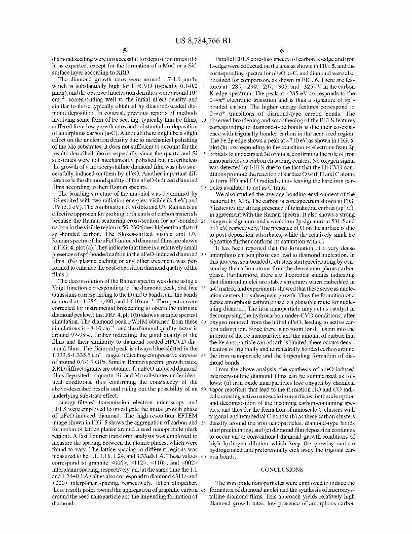
The bonding structure of the material was determined by RS excited with two radiation energies: visible (2.4 eV) and UV (5.1 eV). The combination ofvisible and UV Raman is an effective approach for probing both kinds of carbon materials because the Raman scattering cross-section for sp 2 -bonded carbon in the visible region is 50-230 times higher than that of spa -bonded carbon. The Stokes-shifted visible and UV Raman spectra of the nFeO-induced diamond films are shown in FIG. 4, plot (a). They indicate that there is a relatively small presence of sp 2 -bonded carbon in the nFeO-induced diamond films. (No plasma etching or any other treatment was per-formed to enhance the post-deposition diamond quality of the films.)
The deconvolution of the Raman spectra was done using a Voigt function corresponding to the diamond peak, and five Gaussians corresponding to the D and G bands, and the bands centered at –1,285, 1,490, and 1,610 cm - '. The spectra were corrected for instrumental broadening to obtain the intrinsic diamond peakwidths. FIG. 4, plot (b) shows a sample spectral simulation. The diamond peak FWHM obtained from these simulations is –8-10 crn i , and the diamond quality factor is around 97-98%, further indicating the good quality of the films and their similarity to diamond-seeded HFCVD dia-mond films. The diamond peak is always blue-shifted in the 1,333.5-1,335.5 cm- ' range, indicating compressive stresses of around 0.6-1.7 GPa. Similar Raman spectra, growth rates, XRD diffractograms are obtained for nFeO-induced diamond films deposited on quartz, Si, and Mo substrates under iden-tical conditions, thus confirming the consistency of the above-described results and ruling out the possibility of an underlying substrate effect.
Energy-filtered transmission electron microscopy and EELS were employed to investigate the initial growth phase of nFeO-induced diamond. The high-resolution EFTEM image shown in FIG. 5 shows the aggregation of carbon and formation of lattice planes around a seed nanoparticle (dark region). A fast Fourier transform analysis was employed to measure the spacing between the atomic planes, which were found to vary. The lattice spacing in different regions was measured to be 1. 1, 1. 16, 1.24, and 3.33±0.1 A. These values correspond to graphite <006>, <112>, <110>, and <002> interplanar spacing, respectively, and at the same time the 1.1 and 1.24±0.1 A values also correspond to diamond <311> and <220> interplanar spacing, respectively. Taken altogether, these results point toward the aggregation of graphitic carbon around the seed nanoparticle and the impending formation of diamond.
6 Parallel EELS core-loss spectra of carbon K-edge and iron
L-edge were collected on the area as shown in FIG. 5, and the corresponding spectra for nFeO, a-C, and diamond were also obtained for comparison, as shown in FIG. 6. There are fea-
5 tures at –285, –290, –297, –305, and –325 eV in the carbon K-edge spectrum. The peak at –285 eV corresponds to the 0-70 electronic transition and is thus a signature of sp 2 -
bonded carbon. The higher energy features correspond to O—a* transitions of diamond-type carbon bonds. The
10 observed broadening and smoothening of the EELS features corresponding to diamond-type bonds is due their co-exist-ence with trigonally bonded carbon in the near-seed region. The Fe 2p edge shows a peak at –710 eV as shown in FIG. 6, plot (b), corresponding to the transition of electrons from 2p
15 orbitals to unoccupied 3d orbitals, confirming the role of iron nanoparticles as carbon clustering centers. No oxygen signal was detected by EELS due to the fact that the HFCVD con-ditions promote the reaction of surface O with H and C atoms to form HO and CO radicals, thus leaving the bare iron par-
20 ticles available to act as C traps. We also studied the average bonding environment of the
material by XPS. The carbon is core spectrum shown in FIG. 7 indicates the strong presence of tetrahedral carbon (sp a C), in agreement with the Raman spectra. It also shows a strong
25 oxygen is signature and a weak iron 2p signature at 531.5 and 711 eV, respectively. The presence of O on the surface is due to post-deposition adsorbates, while the relatively small Fe signature further confirms its saturation with C.
It has been reported that the formation of a very dense 30 amorphous carbon phase can lead to diamond nucleation. In
this process, spa-bonded C clusters start precipitating by con-suming the carbon atoms from the dense amorphous carbon phase. Furthermore, there are theoretical studies indicating that diamond nuclei are stable structures when embedded in
35 a-C matrix, and experiments showed that these serve as nucle-ation centers for subsequent growth. Thus the formation of a dense amorphous carbon phase is a plausible route for nucle-ating diamond. The iron nanoparticle may act as catalyst in decomposing the hydrocarbon under CVD conditions, after
40 oxygen removal from the initial nFeO, leading to active car-bon adsorption. Since there is no room for diffusion into the interior of the Fe nanoparticle and the amount of carbon that the Fe nanoparticle can adsorb is limited, there occurs densi-fication of trigonally and tetrahedrally bonded carbon around
45 the iron nanoparticle and the impending formation of dia-mond bonds.
From the above analysis, the synthesis of nFeO-induced microcrystalline diamond films can be summarized as fol-lows: (a) iron oxide nanoparticles lose oxygen by chemical
50 vapor reactions that lead to the formation HO and CO radi-cals, creating active nanoscale iron surfaces for the adsorption and decomposition of the incoming carbon-containing spe-cies, and thus for the formation of nanoscale C clusters with trigonal and tetrahedral C bonds; (b) as these carbon clusters
55 density around the iron nanoparticles, diamond-type bonds start precipitating; and (c) diamond film deposition continues to occur under conventional diamond growth conditions of high hydrogen dilution which keep the growing surface hydrogenated and preferentially etch away the trigonal car-
60 bon bonds.
CONCLUSIONS
The iron oxide nanoparticles were employed to induce the 65 formation of diamond nuclei and the synthesis of microcrys-
talline diamond films. This approach yields relatively high diamond growth rates, low presence of amorphous carbon
US 8,784,766 B1 7
and can be used for the selective diamond deposition and patterning at the nanoscale through dip pen nanolithography of nFeO followed by chemical vapor deposition. The com-bined analysis of the various characterization results, indicate that the iron nanoparticles act as nucleation and aggregation sites for carbon and the impending formation of diamond-type bonds. The formation of a dense, mixed C phase around the Fe nanoparticles leading to the precipitation of spa C bonds is proposed as a plausible explanation for these results.
Although the invention has been described in conjunction with specific embodiments, it is evident that many alterna-tives and variations will be apparent to those skilled in the art in light of the foregoing description. Accordingly, the inven-tion is intended to embrace all of the alternatives and varia-tions that fall within the spirit and scope of the appended claims.
The invention claimed is: 1. A method of synthesizing diamond comprising: depositing iron oxide nanoparticle seeds on a substrate,
said iron oxide nanoparticle seeds being capable of car- bide formation;
and directing a stream of gas composition at the seeded substrate under conditions that effect diamond growth.
2. Themethod of claim 1, wherein said substrate comprises a metal substrate.
3. The method of claim 2, wherein said metal substrate comprises at least one of: copper, molybdenum, aluminum, tantalum, tungsten, and nickel.
4. Themethod of claim 1, wherein said substrate comprises a semiconductor substrate.
5. The method of claim 4, wherein said semiconductor substrate comprises at least one of: silicon, germanium, and gallium arsenide.
6. Themethod of claim 1, wherein said substrate comprises an insulator substrate.
7. The method of claim 6, wherein said insulator substrate comprises at least one of: quartz, glass, gallium nitride, sili-con carbide, and boron nitride.
8. The method of claim 1, wherein said iron oxide nano-particle seeds have a size of about 1 mn to about 50 mu.
9. The method of claim 1, wherein said iron oxide nano-particle seeds have a size of about 4 mn to about 15 mu.
10. The method of claim 1, wherein said iron oxide nano-particle seeds have a surface density of about 10 7 cm2 to about 10 10 cm2 .
11. The method of claim 1, wherein said iron oxide nano-particle seeds have a surface density of about 10 5 cm2 to about 107 cm2 .
8 12. The method of claim 1, wherein once said substrate is
coated, is kept at a temperature of from about 100° C. to about 1000° C.
13. The method of claim 1, wherein once said substrate is 5 coated, is kept at a temperature of from about 400° C. to about
800° C. 14. The method of claim 1, wherein the growth rate for
diamond formation is of about 1.7 Wn/h to about 1.9 µm/h. 15. The method of claim 1, wherein said iron oxide nano-
10 particle seeds are uniformly distributed over the substrate. 16. The method of claim 1, wherein said gas composition
comprises at least one compound having at least one carbon-hydrogen bond; and a diluent gas.
17. The method of claim 16, wherein said at least one
15 compound having at least one carbon-hydrogen bond com-prises methane (CH4).
18. The method of claim 16, wherein said diluent gas is selected from the group consisting of: hydrogen, nitrogen, helium, neon, argon, xenon and krypton.
20 19. The method of claim 1, wherein said substrate has a diameter of about 14 mm and a thickness of about 0.5 mm.
20. The method of claim 1, wherein the step of depositing said iron oxide nanoparticle seeds on the substrate comprises:
coating said substrate with a uniformly distributed iron
25 oxide nanoparticle seeds. 21. The method of claim 1, wherein the step of directing a
stream of gas composition at the seeded substrate comprises: positioning said coated substrate inside a chemical vapor
deposition (CVD) apparatus; and 30 directing a mixture of methane (CH 4) in hydrogen (H z)
over a heated metal filament. 22. The method of claim 21, wherein said heated metal
filament comprises rhenium (Re). 23. The method of claim 21, wherein said heated metal
35 filament is kept at a temperature of about 2700 K and posi-tioned at a distance of about 10 mm above said substrate.
24. The method of claim 21, further comprising: maintain-ing a constant pressure inside said (CVD) furnace of from about 20 Torr to about 50 Torr.
40 25. The method of claim 21, further comprising: maintain- ing said substrate at a temperature of from about 700° C. to about 730° C.
26. The method of claim 1, wherein continuous films of diamond are formed with a thickness of from about 10 µm to
45 about 11 µm. 27. The method of claim 26, wherein said diamond films
have a quality factor of from about 97% to about 98%.