US000008598673B220131203 - NASA · detector for eyesafe LIDAR," Part of SPIE Conference on Laser...
18
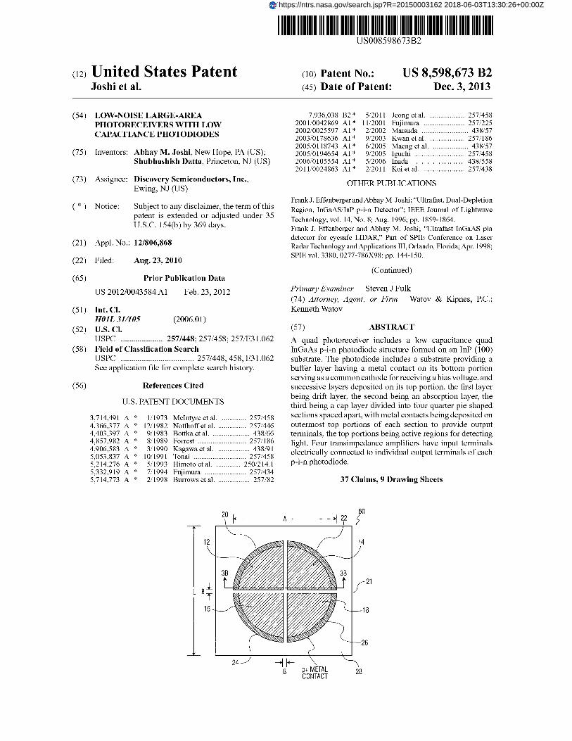
1111111111111111111111111111111111111111111111111111111111111111111111 (12) United States Patent Joshi et al. (54) LOW-NOISE LARGE-AREA PHOTORECEIVERS WITH LOW CAPACITANCE PHOTODIODES (75) Inventors: Abhay M. Joshi, New Hope, PA (US); Shubhashish Datta, Princeton, NJ (US) (73) Assignee: Discovery Semiconductors, Inc., Ewing, NJ (US) (*) Notice: Subject to any disclaimer, the term of this patent is extended or adjusted under 35 U.S.C. 154(b) by 369 days. (21) Appl. No.: 12/806,868 (22) Filed: Aug. 23, 2010 (65) Prior Publication Data US 2012/0043584 Al Feb. 23, 2012 (51) Int. Cl. HOIL 311105 (2006.01) (52) U.S. Cl. USPC .................... 257/448; 257/458; 257/E31.062 (58) Field of Classification Search USPC ................................... 257/448, 458, E31.062 See application file for complete search history. (56) References Cited U.S. PATENT DOCUMENTS 3,714,491 A * 1/1973 McIntyre et al . ............. 257/458 4,366,377 A * 12/1982 Notthoff et al ................ 257/446 4,403,397 A * 9/1983 Bottka et al ..................... 438/66 4,857,982 A * 8/1989 Forrest .......................... 257/186 4,906,583 A * 3/1990 Kagawa et al . ................. 438/91 5,053,837 A * 10/1991 Tonai ............................ 257/458 5,214,276 A * 5/1993 Himotoetal . ............. 250/214.1 5,332,919 A * 7/1994 Fujimura ...................... 257/434 5,714,773 A * 2/1998 Burrows et al .................. 257/82 (1o) Patent No.: US 8,598,673 B2 (45) Date of Patent: Dec. 3, 2013 7,936,038 B2 * 5/2011 Jeong et al . ................... 257/458 2001/0042869 Al* 11/2001 Fujimura...................... 257/225 2002/0025597 Al* 2/2002 Matsuda ......................... 438/57 2003/0178636 Al* 9/2003 Kwan et al .................... 257/186 2005/0118743 Al* 6/2005 Maeng et al . ................... 438/57 2005/0194654 Al* 9/2005 Iguchi ........................... 257/458 2006/0105554 Al* 5/2006 Inada ............................ 438/558 2011/0024863 Al* 2/2011 Koi et al . ...................... 257/438 OTHER PUBLICATIONS Frank J. Effenberger andAbhay M. Joshi; "Uhrafast, Dual-Depletion Region, InGaAS/InP p-i-n Detector'; IEEE Journal of Lightwave Technology; vol. 14, No. 8; Aug. 1996; pp. 1859-1864. Frank J. Effenberger and Abhay M. Joshi; "Ultrafast InGaAS pin detector for eyesafe LIDAR," Part of SPIE Conference on Laser Radar Technology and Applications III, Orlando, Florida; Apr. 1998; SPIE vol. 3380, 0277-786X98; pp. 144-150. (Continued) Primary Examiner Steven J Fulk (74) Attorney, Agent, or Firm Watov & Kipnes, P.C.; Kenneth Watov (57) ABSTRACT A quad photoreceiver includes a low capacitance quad InGaAs p-i-n photodiode structure formed on an InP (100) substrate. The photodiode includes a substrate providing a buffer layer having a metal contact on its bottom portion serving as a common cathode for receiving a bias voltage, and successive layers deposited on its top portion, the first layer being drift layer, the second being an absorption layer, the third being a cap layer divided into four quarter pie shaped sections spaced apart, with metal contacts being deposited on outermost top portions of each section to provide output terminals, the top portions being active regions for detecting light. Four transimpedance amplifiers have input terminals electrically connected to individual output terminals of each p-i-n photodiode. 37 Claims, 9 Drawing Sheets on 60 1 L B: 1 !1 B p+MLIAL 28 CONTACT https://ntrs.nasa.gov/search.jsp?R=20150003162 2018-06-03T13:30:26+00:00Z
Transcript of US000008598673B220131203 - NASA · detector for eyesafe LIDAR," Part of SPIE Conference on Laser...
1111111111111111111111111111111111111111111111111111111111111111111111
(12) United States Patent Joshi et al.
(54) LOW-NOISE LARGE-AREA PHOTORECEIVERS WITH LOW CAPACITANCE PHOTODIODES
(75) Inventors: Abhay M. Joshi, New Hope, PA (US); Shubhashish Datta, Princeton, NJ (US)
(73) Assignee: Discovery Semiconductors, Inc., Ewing, NJ (US)
(*) Notice: Subject to any disclaimer, the term of this patent is extended or adjusted under 35 U.S.C. 154(b) by 369 days.
(21) Appl. No.: 12/806,868
(22) Filed: Aug. 23, 2010
(65) Prior Publication Data
US 2012/0043584 Al Feb. 23, 2012
(51) Int. Cl. HOIL 311105 (2006.01)
(52) U.S. Cl. USPC .................... 257/448; 257/458; 257/E31.062
(58) Field of Classification Search USPC ................................... 257/448, 458, E31.062 See application file for complete search history.
(56) References Cited
U.S. PATENT DOCUMENTS
3,714,491 A * 1/1973 McIntyre et al . ............. 257/458 4,366,377 A * 12/1982 Notthoff et al ................ 257/446 4,403,397 A * 9/1983 Bottka et al ..................... 438/66 4,857,982 A * 8/1989 Forrest .......................... 257/186 4,906,583 A * 3/1990 Kagawa et al . ................. 438/91 5,053,837 A * 10/1991 Tonai ............................ 257/458 5,214,276 A * 5/1993 Himotoetal . ............. 250/214.1 5,332,919 A * 7/1994 Fujimura ...................... 257/434 5,714,773 A * 2/1998 Burrows et al .................. 257/82
(1o) Patent No.: US 8,598,673 B2 (45) Date of Patent: Dec. 3, 2013
7,936,038 B2 * 5/2011 Jeong et al . ................... 257/458 2001/0042869 Al* 11/2001 Fujimura...................... 257/225 2002/0025597 Al* 2/2002 Matsuda ......................... 438/57 2003/0178636 Al* 9/2003 Kwan et al .................... 257/186 2005/0118743 Al* 6/2005 Maeng et al . ................... 438/57 2005/0194654 Al* 9/2005 Iguchi ........................... 257/458 2006/0105554 Al* 5/2006 Inada ............................ 438/558 2011/0024863 Al* 2/2011 Koi et al . ...................... 257/438
OTHER PUBLICATIONS
Frank J. Effenberger andAbhay M. Joshi; "Uhrafast, Dual-Depletion Region, InGaAS/InP p-i-n Detector'; IEEE Journal of Lightwave Technology; vol. 14, No. 8; Aug. 1996; pp. 1859-1864. Frank J. Effenberger and Abhay M. Joshi; "Ultrafast InGaAS pin detector for eyesafe LIDAR," Part of SPIE Conference on Laser Radar Technology and Applications III, Orlando, Florida; Apr. 1998; SPIE vol. 3380, 0277-786X98; pp. 144-150.
(Continued)
Primary Examiner Steven J Fulk
(74) Attorney, Agent, or Firm Watov & Kipnes, P.C.; Kenneth Watov
(57) ABSTRACT
A quad photoreceiver includes a low capacitance quad InGaAs p-i-n photodiode structure formed on an InP (100) substrate. The photodiode includes a substrate providing a buffer layer having a metal contact on its bottom portion serving as a common cathode for receiving a bias voltage, and successive layers deposited on its top portion, the first layer being drift layer, the second being an absorption layer, the third being a cap layer divided into four quarter pie shaped sections spaced apart, with metal contacts being deposited on outermost top portions of each section to provide output terminals, the top portions being active regions for detecting light. Four transimpedance amplifiers have input terminals electrically connected to individual output terminals of each p-i-n photodiode.
37 Claims, 9 Drawing Sheets
on 60
1
L B:
1
!1
B p+MLIAL 28 CONTACT
https://ntrs.nasa.gov/search.jsp?R=20150003162 2018-06-03T13:30:26+00:00Z

US 8,598,673 B2 Page 2
(56) References Cited
OTHER PUBLICATIONS
V. Wand, J. Bogenstahl, C. Braxmaier, K. Danzmann, A. Garcia, F. Guzman, G. Heinzel, J. Hough, O. Jennrich, C. Killow, D. Robertson, Z. Sodnik, F. Steier, and H. Ward; "Noise sources in the UP hetero-dyne interferometer"; Institute of Physics Publishing; Classical and Quantum Gravity 23, 2006; pp. S159-S167.
Abhay Joshi, Shubhashish Datta, and Don Becker; "GRIN Lens Coupled Top-Illuminated Highly Linear InGaAS Photodiodes'; IEEE Photonics Technology Letters, vol. 20, No. 17, Sep. 1, 2008; pp. 1500-1502. Abhay Joshi and Shubhashish Datta; "Dual InGaAs Photodiodes Having High Phase Linearity for Precise Timing Applications"; IEEE Photonics Technology Letters, vol. 21, No. 19, Oct. 1, 2009; pp. 1360-1362.
* cited by examiner
U.S. Patent Dec. 3, 2013 Sheet 1 of 9 US 8 ,598,673 B2
10
1
PD BIAS
42
12
j---------------------------------------1------ I 1 I I 1 I
51 Vout1 PHOTODIOIDE TIA ;
50 48 I 52
L-------- T ---------------------------- --------- ---------1----------------------------1--------- ;
51 Vout2 PHOTODIOIDE TIA
I I
50 48 52 1 I ,
--------1----------------------------; -------- ~
-------- "',---------------------------- + --------- I
50 Vout3 PHOTODIOIDE TIA
51 48 52
I -------- j ----------------------------L --------J
I--------- ----------------------------r-------- -1 ,.18 50
r Vout4
PHOTODIOIDE TIA 1 1
51-)48 ;
52 --------1--------------------------- -------- ~
1
nth PHOTODIODE --- 50 mth TIA --\— 48
FIG. 1
U.S. Patent Dec. 3, 2013 Sheet 2 of 9 US 8,598,673 B2
AFB - 0.2pF (48
1
RFB = 51 kn
44 PIN PD (ONE QUADRANT)
PD BIAS RPD W rill INEQ
42
BPD =2.5 pF
50
FET-INPUT OpAmp ------------------,
INA
CAMP
'-------------J---- 46
47
VOUT
52
FIG. 2

21
8
5
1.
L B:
1
InP CAP LAYER i In0.53Ga0.47As 34 h le ABSORPTION LAYER
i InP 36 DRIFT LAYER
n+ InP 38 BUFFER LAYER
n+ InP 39 (100) SUBSTRATE
n+ METAL BACK CONTACT (COMMON CATHODE)
C
D
E
Ak
H ir
40
-~— G
TOTAL F DEPLETION
REGION
~ I T
FIG. 313
U.S. Patent Dec. 3, 2013 Sheet 3 of 9
US 8,598,673 B2
20 1. ` i 00 60
B p+ MLIAL 28 CONTACT
FIG. 3A
P+ METAL 32B
22 60 CONTACT 35 64 —~~`— 28 20 -FI /-)
6
5 LL_
°- 4 W U
3 U
2 U
110
102 0 L 0
6
5
°- 4 W U
3 U
Q 2 U
1
0
15 106
10
z O
5 W 0
U.S. Patent Dec. 3, 2013 Sheet 4 of 9 US 8 ,598,673 B2
104 X 100 I I 1 1 I ilk 1 1 I 1 1 1 1
I I I I 1 1 I I I I I I I ✓
I I I I r ✓ I I ~ I I I ~ ✓ ~ I I
---- I I
I/ I ~ ✓ I I I y ✓ 1 I 1 I ~ I_
- - I _ ------ 'I if
.01 1
CI~ I
IL 1 ______L__-- ____ ____ L______ L______ L______ L ------
I I I I I I I I I I I I I I I I
JU 16
I I I I I 1 I I
I I I I 1 I I I I I I I I I 1 I I I I I
I I I I I I I 1 I I I 1
I ~ I ~
I I 1 i 1
-1 --I - r ---- ----- { I 1 I I I I 1
I I I I I I I 1 I 1 I I I I
------;-------;-------L------L------;------;------L------ ~ I I I I I I I I I I I 1 I I I I I I I I I
I I I 1 1 l
4 8 12 REVERSE BIAS (V)
1 ~
Q-- QUADRANT 12 ~--- QUADRANT 14
--0-- QUADRANT 16 ~-- QUADRANT 18
sae
FIG. 4A
~ 0 4 12 REVERSE BIAS (V) 16 FIG. 413
300
Q
-o--QUADRANT 12
~ ---- QUADRANT 14 --0-- QUADRANT 16
I I I 1 I 1 1 I I I
1 I 1 1 1 1 I 1 I I I 1 I
1
I I 1 I 1
w 200
U C= 100 Q
0
I I 1 I 1 I I 1 1
- QUADRANT 18 ------------ --- --------- I I I I I I I I I
I I I I 1 I 1 I
-----1----1----L--- - ------J-----1-----I- -
1 I 1 I I I 1 I I I I I 1 I I I I I I I
L ---- L ---- 1 ---- L ---- 1 ---- J ---- J---- J ----- 1_____I_____ I I I I I I I 1 I I I I I I 1 1 I I 1 I I I I I 1 I I I 1 I I I I I 1 I I I 1
I I 1 I 1 I 1 I 1 I i I 1 I I I I I 1 I I I 1 I I I 1 I 1 I 1 I 1 1 I I 1 I 1
° 4 8 12 16 2° FIG. 4C REVERSE BIAS (V)

N
Q
V J
Z w im
W C/)
C) z
Z W
U
a. z
10-2
10-2
10-3 0.1
102
10 1
100
I I I 1 1 1 1 1 1 1 I I 1 1 1 1 1 1 1 I I 1 1 1 1 1
I I I 1 1 1 1 1 1 I I
I 1 1 1 I I III I I
I 1 1 1 1 1 1
I I I I111
7 I 51.3
•
M HL 1 I I 1 1 1 I I I I I I 1 1 1 1 1 1 I
I I
---1- LO SHOT NOISE I 1 1 1 1 1 1 1 I I I I I I I
1 I 1 1 1 1 I I I I 1 I I
1 I I 1 1 1 1 1 1 I I I 1 1 1 1 1 1 I 1 I I I I I
1 I I 1 1 1 1 1 1 I 1 1 1 1 1 1 1 1 I I I I I I I
I I I 1 1 1 1 1 1 I 1 1 1 1 1 1 1 1 i I I I I I I
I I I 1 1 1 1 1 1 I I
Lill ----- 4 ---
L-1-J-1J-LL
----- L--J--1
111
I 1 1 1 1 1 1 I 1 I I I I I I
II 1 1 1 1 1 1 1
i--1-a-1-1-144
-- It I 1 I I 1 - •--- I
--I - T1-I-nT ---- r -- r - r - rrrr --- 'I-----I-
I I I 1 1 1 1 1 1 I 1
I -
- I I 11 I • I I II -' I ~ I I ~ h i l ll •- •1 I ~ I I I I I-
-
- - rn --- 1 -- r - I - r rrl --- T --1 - T -I - I -IIr
I 1 1 1 1 1 1 1 1 I I I 1 1 1 1 1 I 1 1 1 1 1 11'
I 1 1 1 1 1 1 1 1 I I I 1 1 1 I I I I 1 I I I I I I
--- --
--I -- I I 1 1 1 1 1 1
I I I I I I 11 1 1 I I I 1 I I I_
I 1 1 1 1 1 1 1 I I I I11111 I I I I I III-
I I 1 1 11 1 1 I I
- - -
I111111 I
I 11 1 11 1 1 11 ............. ........................................................................... 1111111 11 ............................... 11111111 11 11 1 11 1 1 1111 1 1 1 1_
I I I 1 1 1 I I I I I I 1 1 1 1 1 1 I 1 I I I 1 1 1
1 10 FREQUENCY (MHz)
100
U.S. Patent Dec. 3, 2013 Sheet 5 of 9
US 8,598,673 B2
OpAmp VOLTAGE NOISE -- ---- RFg THERMAL NOISE
............ OpAmp CURRENT NOISE — - IDARK SHOT NOISE RpD THERMAL NOISE TOTAL EXCESS NOISE
FIG. 5A

N
Q
U~ z w Cn
w U_)
C) z
Z w
L= U
Cl- z
10-2
10-2
L 10-30.1
102
10 1
100
I I 1 1 1 1 1 11 I I I I i l l l l I I 1 1 1 1 1 1
9.8 MHz: I I I 1 1 1 1 1 1 I I I 1 1 1 1 1 1 I I 1 1 1 1 1
I
---L LO SHOT NOISE
I I I I I I I
-L _I_L LLIJ
I
_ I_J-
1 1 1 1 1 1 I_I_IJL
_-----L--J--L-LJ-1111----- 1---L-J-J_LJ1 -----L--J--i-L-LiJJ I I I 1 1 1 1 1 1 1 1 I I I I I 1 I 1 I I I I I I 1 1 1 1 1 1 I 1 I 1 1 1 1 1 I 1 I I 1 1 I I I 1 1 1 1 1 1 1 1 1 1 1 1 1 1 I I I I I I
I I I 1 1 1 1 1 1 I 1 1 1 1 1 1 1 I I I I I I I
:---r - 7 - r7tiyrn - --r -I - rrrlyr --' --I - Y -1 - I- Itir I I I I 1 1 1 1 1 1 1 I 1 I I I I I
-----~ --r-~ -r -I -~ - -- - r--r-r -r rrr ---- I- - -1--~ 1 I 1 I I I I I
1 11L. — .J— . 1_1.111. LL I I 1 1 1 1 1 1 I I 1 1 1 1 1 1 1 I 1 I I I I I
I I 11 1 1 1 1 I - -- r - ~ - r~ ~ ern --- 1 -- r - I - r rrrlr - - -
I I I 1 1 1 1 1 1 1 1 I 1 1 1 1 1 1 1 I I I I I I I
I I I I I I I 1 1 I 1 1 1 1 1 1 I I 1 1 1 1 1 1
I I I I 1 1 1 1
r -- I --r
I t I 1 1 1 1 1 1 I I 1 1 1 1 1 1
I I 1 1 1 1 1 1 1 1 I 1 1 1 1 1 1 I I 1 1 1 1 1 1
_J_LJ JJ1-u-- -J_-L J_L LLUL-- _1_J_J J_IJJL I I I I I I I I I 1 1 1 1 1 1 1 1 1 I 1 1 1 1 1 1 1
I I IIIII II 1 111 1 1 1 1 1 11 111111
...........I...... J.... 1 ... 1..l..l..l.1.1...........1......1....1... J...l.I.l...........1.......1....1... L..I..l.l.l. 1 I I 1 1 1 1 1 1 I I 1 1 1 1 1 1
I 1 I 1 1 1 1 1 1 1 I I 1 1 1 1 1 1 I I 1 I I I I I
1 10 FREQUENCY (MHz)
FIG. 5B
100
U.S. Patent Dec. 3, 2013 Sheet 6 of 9
US 8,598,673 B2
OpAmp VOLTAGE NOISE ------ RFg THERMAL NOISE OpAmp CURRENT NOISE - - IDARK SHOT NOISE RpD THERMAL NOISE TOTAL EXCESS NOISE

U.S. Patent Dec. 3, 2013 Sheet 7 of 9
US 8,598,673 B2
40
z 30 lQ V
z 0 20 C/)
W
0 10 U
0
__ ---.- ... . ______l_____ I J______ 1______ L______I_. I I I I 1 -- ~~ . ®- .... d
d I I I I I I I 1 1 I 1 .,. I I I
1 I I I I I I I I I
I I I 1 I I I I I.--
•
I I I I I 1 I I I 1 II I I 1 L_____ J______ 1______ L_____ I.
1 I I 1 I 1 I I 1 1 1 I I 1 1 1 I 1 1
1 I I I 1 1 1 I I 1
1 I I I 1 I I I I 1 1 1 I I 1
T ______ r _____ -
_. I 1 1 I 1 I 1 I I 1
I I I I 1 I 1 1 I 1
I I I I I I I I I 1 I I I I 1 I 1 I I 1 I I I I I I I I I 1
0 4 8 12 16 20 FREQUENCY (MHz)
FIG. 6A
I I I I
i I
I I
N
a 3 Q
z U-j 2 0 w Cn 0 Z
z 1 LLB Cx-_M C= U
~ 0 Z
I I I 1 I I I I I I I I I I I 1 1 1 1
I 1 1 1 1
---- - 0- QUADRANT 12 ___ T - - - - - - r - - - - - -r- - - - -T - - - - - - - - - ,-" I 1 I I 1
~ .... QUADRANT 14 I 1 I I 1 ______L______I__
c ------ IL --0-- QUADRANT 16 ' I 1 I I 1
I 1 1 I 1 I I I 1 I 1
---- QUADRANT 18 --- ----- ----- ------ 1 ------L ----- -- I 1 1 1 1 I 1 I I 1 1
I I 1 1 1 1 1 I 1 I I I 1 1 1 I I 1
J_ I _____ 1______ L_____ ___1 ------ L_____J ------ 1 ------ L------ I 1 I 1 I I I 1
I I 1 I 1 1 I 1 1
I I 1 I 1 1 I I 1 I I 1 I I I I I 1 ___L ----- J ------ 1 ------ L ------ 1______1______L______1_. I I I I I 1 I I I I 1 1 I I I I I I
I 1 1 I I I I I I I I 1 I 1 1 I I 1
I I 1 1 I 1 1 I I 1 J_ I_____1______I______J______1
------ L 1 _____J 1______1 I ______ IL ------ I I I I 1
I I I I I I 1 I I I I I I I I i 1 I I 1 I I I I I 1 1 I I 1 1 I I I I 1 1 I I 1
0 4 8 12 16 20 FREQUENCY (MHz)
FIG. 6B

-3 N
Q Q
W
0 2 z
z
z Lu 1 __j
`J
Lu
0 1 0
U.S. Patent Dec. 3, 2013 Sheet 8 of 9 US 8,598,673 B2
I I I I I I I 1 1 1 I I I 1 1 1 1 1 1 I I I 1 I 1 I 1 1 I I I I I I 1 1 I 1 I I I 1 I 1 I
I I I I 1 1 t 1 t I 1 I I I I 1 1 1 I I I I I I 1 I 1 I 1 I I I I 1 I 1 I I I I I I I I 1
I I I I I I I I I I I 1 I I I I I I I I 1 I I I I I I I I I I I I I I I I I I I I I I I I I I I 1 I I I I I
1 I I 1 I 1 I I I I I I I I I I I 1 1 I I 1 1 I I I I I I I 1 I 1 I I I 1 I I 1 I I I I I
I I I I I I I I I I I 1
° b o o ° I ° Q ° I I 1 1
I I I I I I I 1 1 I I I I I I I 1 1 I I I I I I I 1 1 I I 1 I I I I 1 1 I I 1 I I I 1 1 1
I
I I i I I I 1 1 I I I I I I I 1 t 1 I I 1 I I I 1 1 1 I I 1 I I I 1 1 I I I 1 I I I 1 1 1 I I I 1 I I 1 1 1
12
16 20 FREQUENCY (MHz)
FIG. 7

U.S. Patent Dec. 3, 2013
Sheet 9 of 9
US 8,598,673 B2
S
112 ~. 118
118 118 114
118
114
86
813
118
28
40
FIG. SA
p+ METAL 114 P+ Zn ANTI-REFLECTION
114
CON TACT
TACT B
DIFFUSION 114 COATING 6 116
112 28
C D
E
/-40
n+ METAL BACK CONTACT (COMMON CATHODE) FIG. 813
InP CAP LAYER i In0.53Ga0.47As 34 h e ABSORPTION LAYER
i InP 36 DRIFT LAYER
n+ InP 38 BUFFER LAYER
n+ InP 39 (100) SUBSTRATE
~ _L G
TOTAL F DEPLETION
REGION
US 8,598,673 B2
LOW-NOISE LARGE-AREA PHOTORECEIVERS WITH LOW CAPACITANCE PHOTODIODES
GOVERNMENT INTEREST
This invention was made with government support under U.S. (Agency) Contract No. NNX09CD48P awarded by the NASA/Goddard Space Flight Center. The government has certain rights in the invention.
FIELD OF THE INVENTION
The present invention relates to semiconductor devices, and more particularly, to both photoreceivers, and to p-i-n photodiodes.
BACKGROUND OF THE INVENTION
Quad photoreceivers typically include a 2x2 array of p-i-n photodiodes with each photodiode followed by a transimped-ance amplifier (TIA). Such quad photoreceivers are used in many applications, such as long baseline interferometry, free-space optical communication, missile guidance, and bio-medical imaging and spectroscopy, which rely on free-space optical propagation with position and/or direction sensing capability. It is desirable to increase the active area of quad photoreceivers (and photodiodes) to enhance the link gain, and therefore sensitivity, of the system. However, the result-ing increase in the photodiode capacitance reduces the band-width of the photoreceiver and adds to the equivalent input current noise, especially at high frequencies, for a given volt-age noise level of the TIA.
In fact, the capacitance of the photodiode and its excess current noise arising therefrom, scales linearly as the device area, thereby negating the corresponding increase in the link gain. Owing to this contradiction, the front-end quad photo-receiver can limit the sensitivity of the overall system. An example of such an application is the Laser Interferometry Space Antenna (LISA), which proposes to detect gravity waves in space by measuring distance with —10 µm/ -VHz accuracy over a baseline of five million kilometers. The present invention, as described herein relative to quad photo-receivers, is applicable for use in LISA which requires use of low-noise large-area photoreceivers, based on low-capaci-tance large-area photodiodes, for free space applications.
In LISA, the optical local oscillator (LO) power incident on each photoreceiver quadrant will be restricted to 100 µW to minimize the power requirements and thermal fluctuations for high pathlength stability. Assuming a photodiode respon-sivity of 0.7 A/W at 1064-nm wavelength, the desired shot noise-limited system operation requires the photoreceiver to display an equivalent input current noise density of <4.7 pA/-VHz per quadrant. For 0.9-A/W photodiode responsivity at 1550-nm wavelength, an equivalent input current noise density of <5.4 pA/-VHz is needed. Currently, LISA's sensi-tivity is restricted by the noise arising from 20- to 25-pF capacitance per quadrant demonstrated by typical 1-mm-di-ameter InGaAs quad photodiodes.
Accordingly, there is a need for photoreceivers having associated low capacitance photodiodes to achieve enhanced sensitivity. There is also a need for low capacitance photo-diodes for many other applications that can be provided indi-vidually or in an array. The present inventors urge that such applications include systems relying on coherent optical detection, such as LISA, as well as those utilizing direct detection.
2 SUMMARY OF THE INVENTION
A quad photoreceiver for a first embodiment of the inven-tion includes four p-i-n photodiodes formed on a common n'
5 doped InP (100) substrate serving as a buffer layer with a bottom metal layer contact providing a common cathode for receiving a bias voltage, a first i-InP drift layer is deposited on the buffer layer, followed by an i-InGaAs absorption layer, followed by an InP cap layer divided into four spaced apart
10 p'-doped sections, with the p' doping extending into a top most underlying portion of the absorption layer. Each cap section quadrant has p' metal contacts deposited on top out-ermost portions thereof to serve as respective output termi-
15 nals, and the top portions of each quadrant providing an active region responsive to light signals. Four transimpedance amplifiers have individual input terminals electrically con-nected to the output terminals of each cap section quadrant, respectively.
20 A second embodiment of the invention includes an indi-vidual p-i-n photodiode formed as in the above-described first embodiment of the invention, for applications requiring low capacitance photodiodes.
A third embodiment of the invention includes a photore-25 ceiver comprising a single p-i-n photodiode of the second
embodiment driving a TIA. A fourth embodiment of the invention includes an array of
at least two of the low capacitance p-i-n photodiodes of the first embodiment.
30
BRIEF DESCRIPTION OF THE DRAWINGS
The following drawings are illustrative of embodiments of the present invention and are not intended to limit the inven-
35 tion as encompassed by the claims forming part of the appli-cation.
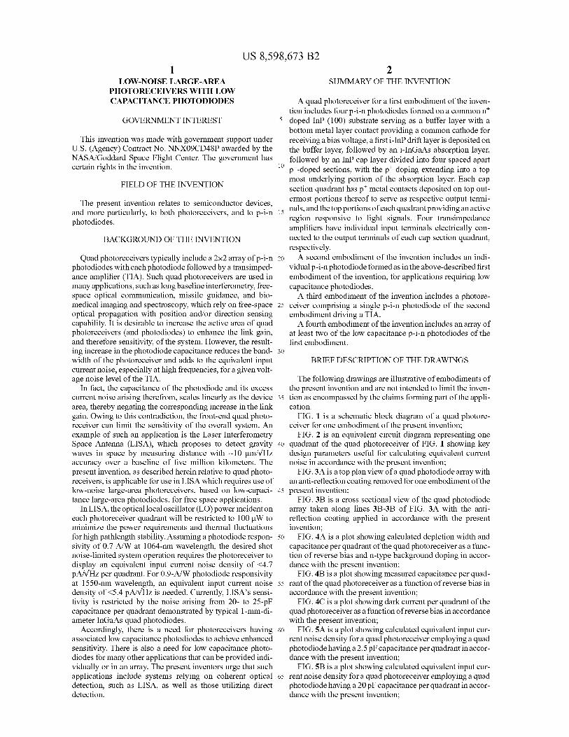
FIG. 1 is a schematic block diagram of a quad photore-ceiver for one embodiment of the present invention;
FIG. 2 is an equivalent circuit diagram representing one 4o quadrant of the quad photoreceiver of FIG. 1 showing key
design parameters useful for calculating equivalent current noise in accordance with the present invention;
FIG. 3A is a top plan view of a quad photodiode array with an anti-reflection coating removed for one embodiment of the
45 present invention; FIG. 3B is a cross sectional view of the quad photodiode
array taken along lines 313-313 of FIG. 3A with the anti-reflection coating applied in accordance with the present invention;
50 FIG. 4A is a plot showing calculated depletion width and capacitance per quadrant of the quad photoreceiver as a func-tion of reverse bias and n-type background doping in accor-dance with the present invention;
FIG. 4B is a plot showing measured capacitance per quad-55 rant of the quad photoreceiver as a function of reverse bias in
accordance with the present invention; FIG. 4C is a plot showing dark current per quadrant of the
quad photoreceiver as a function of reverse bias in accordance with the present invention;
60 FIG. 5A is a plot showing calculated equivalent input cur- rent noise density for a quad photoreceiver employing a quad photodiode having a 2.5 pF capacitance per quadrant in accor-dance with the present invention;
FIG. 5B is a plot showing calculated equivalent input cur- 65 rent noise density for a quad photoreceiver employing a quad
photodiode having a 20 pF capacitance per quadrant in accor-dance with the present invention;

US 8,598,673 B2 3
FIG. 6A is a plot showing measured conversion gain at 1550-mu wavelength per quadrant of the quad photoreceiver in accordance with the present invention;
FIG. 6B is a plot showing measured equivalent input cur-rent noise density per quadrant of the photoreceiver based on a low noise FET input OpAmp in accordance with the present invention;
FIG. 7 is a plot showing measured equivalent input current noise density for one quadrant of a 1-mm diameter quad photoreceiver based on a low noise bipolar input OpAmp with the solid black line showing the theoretical simulation, while the open circles show the actual measured results;
FIG. 8A shows a pictorial view of an array of S rows and T columns of photodiodes in accordance with one embodiment of the present invention; and
FIG. 8B is a cross sectional view taken along lines 813-813 of FIG. 8A.
DETAILED DESCRIPTION OF THE INVENTION
The present invention is directed to a quad photoreceiver based on low-capacitance quadphotodiodes eachfollowedby a transimpedance amplifier. In one embodiment of the present invention, there is provided a 1-mm-diameter InGaAs quad photodiode having 2.5-pF capacitance per quadrant. In con-junction with low-noise field effect transistor (FET)-input operational amplifiers, the associated low-capacitance quad photodiodes are each designed to provide a quad photore-ceiver having an equivalent input current noise density of less than 3.2 pA/-VHz per quadrant up to a 3-dB bandwidth of -20 MHz. This constitutes up to -17-dB improvement in sensi-tivity over a quad photodiode having 20-pF capacitance per quadrant.
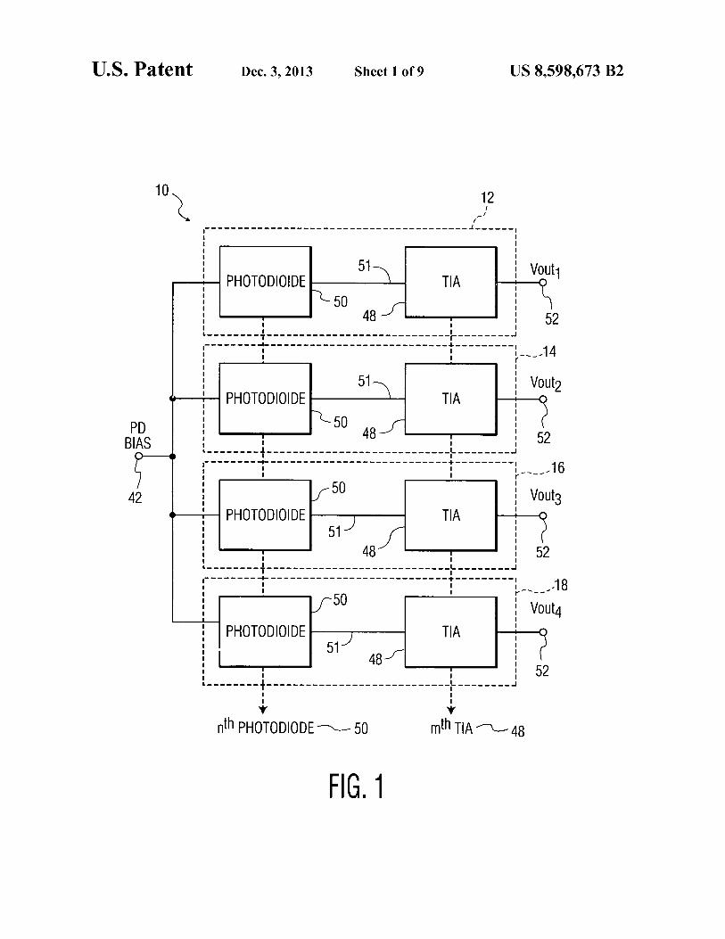
Referring to FIG. 1, a schematic block diagram of a quad photoreceiver 10 is shown for one embodiment of the present invention. The quad photoreceiver 10 includes four quadrants or sections 12, 14, 16, and 18 each having a photodiode 50 followed by a transimpedance amplifier (TIA) 48, and an output terminal (Vout) 52 for supplying an output signal from each quadrant 12, 14, 16 or 18, and a common input terminal 42 for providing a common cathode to supply a bias voltage to each of the photodiodes 50. Each of the transimpedance amplifiers 48 includes individual input terminals electrically connected to the output terminals of each photodiode 50, respectively, via a conductor 51. In one embodiment of the present invention, the photodiodes 50 of the quadrants 12, 14, 16, or 18 are fabricated from a quad InGaAs photodiode array 60 (see FIGS. 3A-313) as will be described hereinafter. It is noted that the photoreceiver 10 of the present invention is shown having four quadrants for purposes of description and is not limited to such a number. Thus, the present invention is intended to encompass embodiments of at least one quadrant or a plurality of quadrants.
FIG.1 is also extended to show an array of photodiodes 50 up to a limit of (value ofn2, 3, 4.... ), coupled individually to associated transimpedance amplifiers 48 up to a limit of m (value of m=2, 3, 4, ... ), respectively. In this manner an array of photoreceivers 10 can be provided. Also, a single photo-diode 50 can be provided a bias voltage, and used to drive a single TIA 48 for providing a photoreceiver (n=1, m=1).
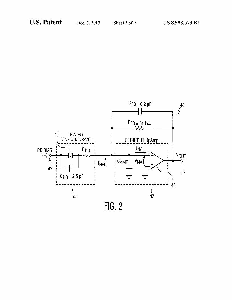
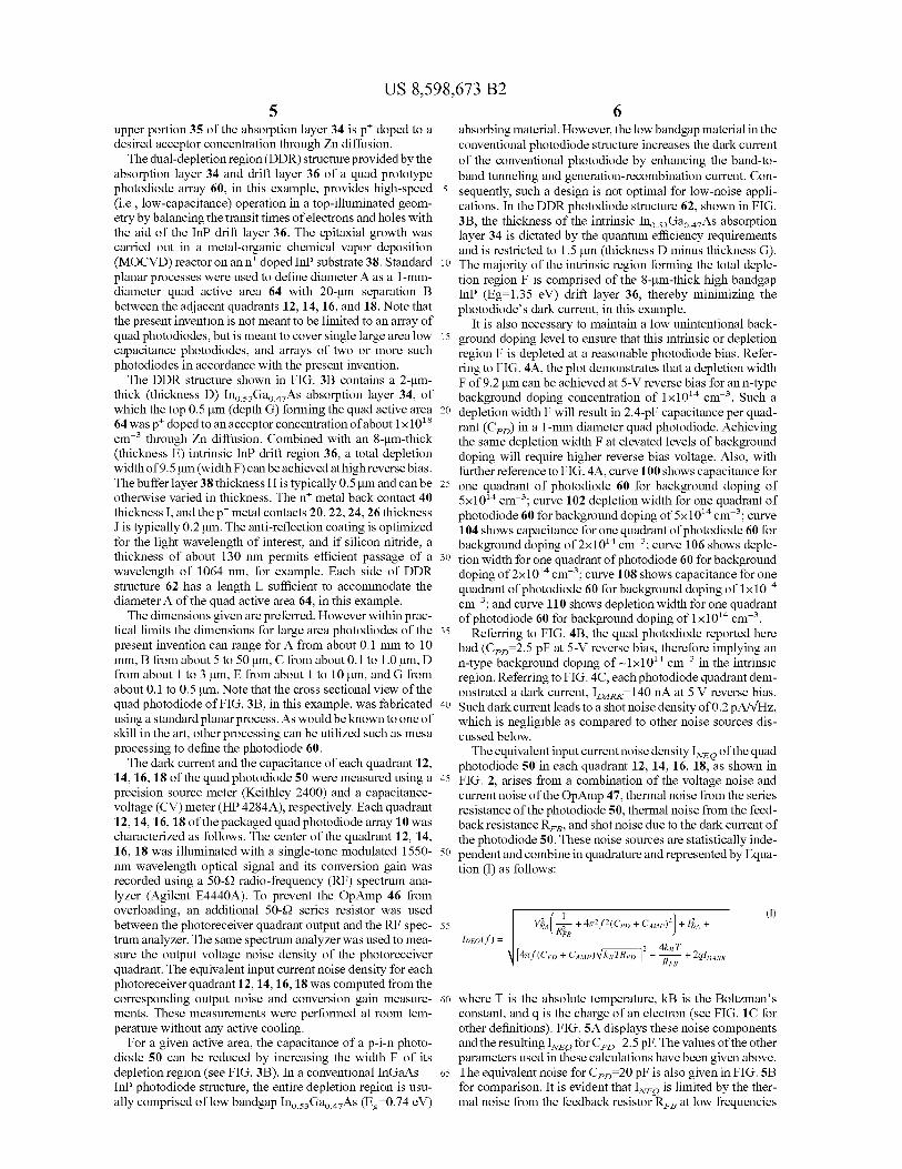
Referring to FIG. 2, an equivalent circuit of a single quad-rant 12, 14, 16, or 18 of the quad photoreceiver 10 of FIG. 1 is shown with key design parameters useful for calculating equivalent current not se in accordance with the present inven-tion. Each quadrant 12, 14, 16, or 18 includes a p-i-n photo-diode 50 electrically coupled at its output terminal to the input terminal of an associated transimpedance amplifier (TIA) 48.
4 Each photodiode 50 further includes an input terminal 42 for providing a common cathode to receive a bias voltage, a diode 44 connected in parallel to a capacitor C D, and a resistor R D
having one end connected to the common connection of the 5 anode of diode 44 and capacitor C D .
The TIA 48 includes a 51-k-Q) feedback resistance RPB and -0.2 pF of feedback capacitance CPB in conjunction with an FET-Input operational amplifier (OpAmp) 47. An output end resistor R D is connected to the inverting input of ampli-
10 fier 46. A suitable example of the OpAmp 47 is an ADA4817 FET-input operational amplifier commercially available from Analog Devices, Inc. of Norwood, Mass. The nominal OpAmp 47 parameters, relevant for noise calculations,
15 include input voltage noise density V, ,A=4 nV/-VHz, input current noise density I,,A 2.5 fA/ -VHz, and input capacitance CAS 1.4 pF. The photodiode 50 of the quadrant 12, 14,16 or 18 is characterized by its capacitance C D and series resis-tance R D (-1 OQ). The quad photoreceiver 10 was assembled
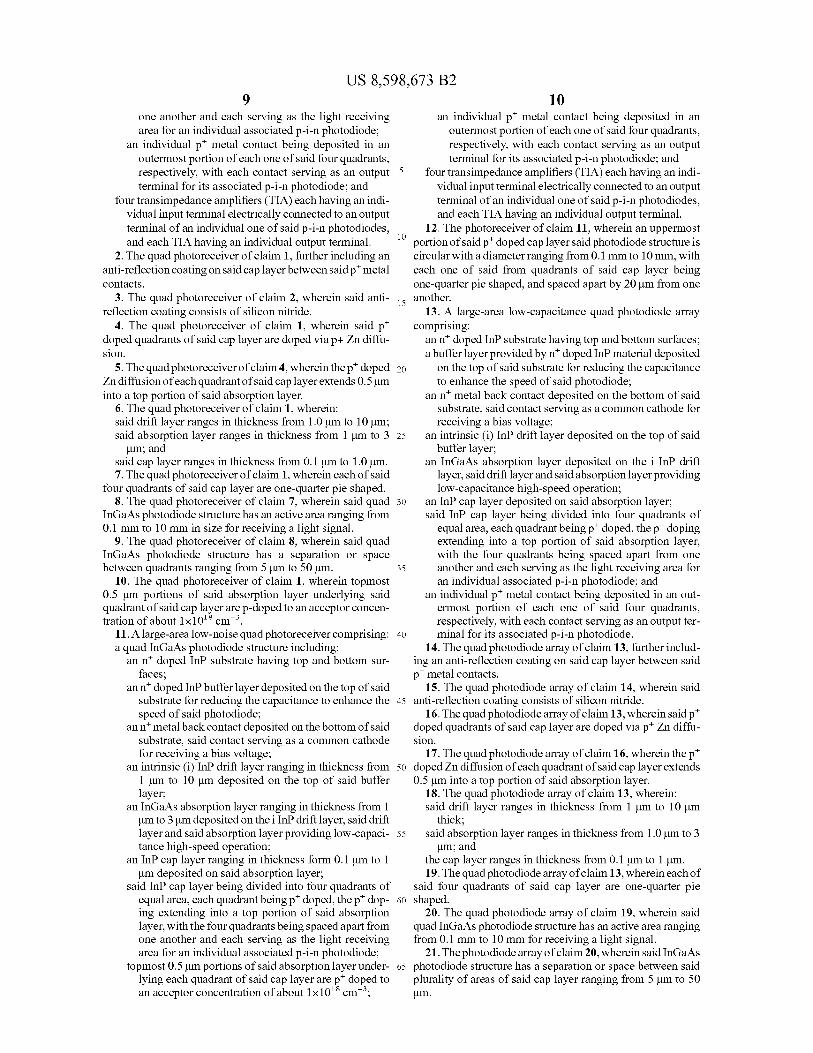
20 in a standard TO-3 package for device testing. Referring to FIGS. 3A and 313, a quad photodiode array 60
including a quad InGaAs photodiode structure is shown for one embodiment of the present invention. The quad photo-diode array 60 is based on the top-illuminated dual-depletion
25 region (DDR) design. The quad photodiode array 60 includes four p-i-n photodiodes 50 formed on a common n' InP (100) substrate 39 with a buffer layer 38 of thickness H deposited thereon. A metal layer contact 40 is deposited on the bottom of the substrate 39 to provide a common cathode for receiving
3o a bias voltage, a first i-InP drift layer 36 of thickness E deposited on the buffer layer 38, followed by an i-InGaAs absorption layer 34 of thickness D, followed by an InP cap layer 28 of thickness C divided into four p'-doped quarter pie sections or quadrants 12, 14, 16, and 18, each with an active
35 region 64 having p' doping extending into a top most under-lying portion 35 of the absorption layer 34, each serving as a photodiode 50. The combination of the absorption layer 34 and the drift layer 36 forms a total depletion region of thick-ness F. Note that the buffer layer 38 can be provided as part of
40 orintegral with substrate 39, thereby saving a deposition step. The quadrants 12, 14, 16, and 18 are characterized by a
diametric size A where each quadrant 12, 14, 16, or 18 is spaced from one another by length B. An anti-reflection coat-ing 32 of predetermined thickness overlays the top portions of
45 the activeregions 64, and consists of a silicon nitride material in this example. Other examples of suitable anti-reflection coating include, for example, silicon dioxide.
Each cap section or quadrant 12, 14, 16, and 18 has a p' metal contact 20, 22, 24, and 26, respectively, deposited on
50 top outermost portions thereof to serve as respective output terminals. The top portions of each quadrant 12,14,16, or 18 provide active regions 64 responsive to light signals. Each of the p-doped active areas 64 of the quadrants 12,14,16, and 18 together with metal contacts 20, 22, 24, and 26, the absorption
55 layer 34, the drift layer 36, the buffer layer 38, and metal back contact 40, operates as a single p-i-n junction photodiode 50 shown in FIG. 2. Four transimpedance amplifiers 48 (not shown) include individual input terminals electrically con-nected to the output terminals in the form of the metal con-
60 tacts 20, 22, 24, and 26, of each cap section or quadrant 12, 14, 16, or 18, respectively.
In one embodiment of the present invention, the cap layer 28 is composed of indium phosphide (InP). The absorption layer 34 is composed of intrinsic (i) In 0 53Gao 47As. The drift
65 layer 36 is composed of intrinsic indium phosphide (i InP). The buffer layer 38 is composed of n' doped indium phos- phide. The quad active area 64 of the cap layer 28 and the
US 8,598,673 B2 5
upper portion 35 of the absorption layer 34 is p + doped to a desired acceptor concentration through Zn diffusion.
The dual-depletion region (DDR) structure provided by the absorption layer 34 and drift layer 36 of a quad prototype photodiode array 60, in this example, provides high-speed 5 (i.e., low -capacitance) operation in a top-illuminated geom-etry by balancing the transit times of electrons and holes with the aid of the InP drift layer 36. The epitaxial growth was carried out in a metal-organic chemical vapor deposition (MOCVD) reactor on an n + doped InP substrate 38. Standard io planar processes were used to define diameter A as a 1-mm-diameter quad active area 64 with 20-M separation B between the adjacent quadrants 12, 14 , 16, and 18. Note that the present invention is not meant to be limited to an array of quad photodiodes , but is meant to cover single large area low 15 capacitance photodiodes, and arrays of two or more such photodiodes in accordance with the present invention.
The DDR structure shown in FIG. 3B contains a 2-µm-thick (thickness D) Ino.53Gao 47As absorption layer 34, of which the top 0.5 µm (depth G) forming the quad active area 20 64 was p+ doped to an acceptor concentration of about 1 x 10 18 CM-3 through Zn diffusion. Combined with an 8-µm-thick (thickness E) intrinsic InP drift region 36, a total depletion width of 9.5 µm (width F) can be achieved at highreverse bias. The buffer layer 38 thickness H is typically 0.5 µm and can be 25 otherwise varied in thickness. The n+ metal back contact 40 thickness I, and the p + metal contacts 20, 22 , 24, 26 thickness 7 is typically 0.2 µm. The anti -reflection coating is optimized for the light wavelength of interest, and if silicon nitride, a thickness of about 130 mu permits efficient passage of a 30 wavelength of 1064 mu, for example. Each side of DDR structure 62 has a length L sufficient to accommodate the diameter A of the quad active area 64, in this example.
The dimensions given are preferred. However within prac-tical limits the dimensions for large area photodiodes of the 35 present invention can range for A from about 0.1 mm to 10 mm, B from about 5 to 50 µm, C from about 0.1 to 1.0 µm, D from about 1 to 3 µm, E from about 1 to 10 µm, and G from about 0.1 to 0.5 µm. Note that the cross sectional view of the quad photodiode of FIG. 313, in this example, was fabricated 40 using a standard planar process . As would be known to one of skill in the art, other processing can be utilized such as mesa processing to define the photodiode 60.
The dark current and the capacitance of each quadrant 12, 14, 16 , 18 of the quad photodiode 50 were measured using a 45 precision source meter (Keithley 2400) and a capacitance-voltage (CV) meter (HP 4284A), respectively. Each quadrant 12, 14, 16, 18 of the packaged quad photodiode array 10 was characterized as follows. The center of the quadrant 12, 14, 16, 18 was illuminated with a single -tone modulated 1550- 50 mu wavelength optical signal and its conversion gain was recorded using a 50-Q radio -frequency (RF) spectrum ana-lyzer (Agilent E4440A). To prevent the OpAmp 46 from overloading , an additional 50-Q series resistor was used between the photoreceiver quadrant output and the RE spec- 55 trum analyzer . The same spectrum analyzer was used to mea-sure the output voltage noise density of the photoreceiver quadrant. The equivalent input current noise density for each photoreceiver quadrant 12,14,16,18 was computed from the corresponding output noise and conversion gain measure- 60 ments. These measurements were performed at room tem-perature without any active cooling.
For a given active area , the capacitance of a p-i-n photo-diode 50 can be reduced by increasing the width F of its depletion region (see FIG. 313). In a conventional InGaAs 65 InP photodiode structure , the entire depletion region is usu-ally comprised of low bandgap Ino.53Gao 47As (Eg-0.74 eV)
6 absorbing material. However, the low bandgap material in the conventional photodiode structure increases the dark current of the conventional photodiode by enhancing the band-to-band tunneling and generation -recombination current. Con-sequently, such a design is not optimal for low -noise appli-cations. In the DDR photodiode structure 62, shown in FIG. 313, the thickness of the intrinsic In 0 53 Gao 47As absorption layer 34 is dictated by the quantum efficiency requirements and is restricted to 1.5 µm (thickness D minus thickness G). The majority of the intrinsic region forming the total deple-tion region F is comprised of the 8 -µm-thick high bandgap InP (Eg=1.35 eV) drift layer 36, thereby minimizing the photodiode's dark current, in this example.
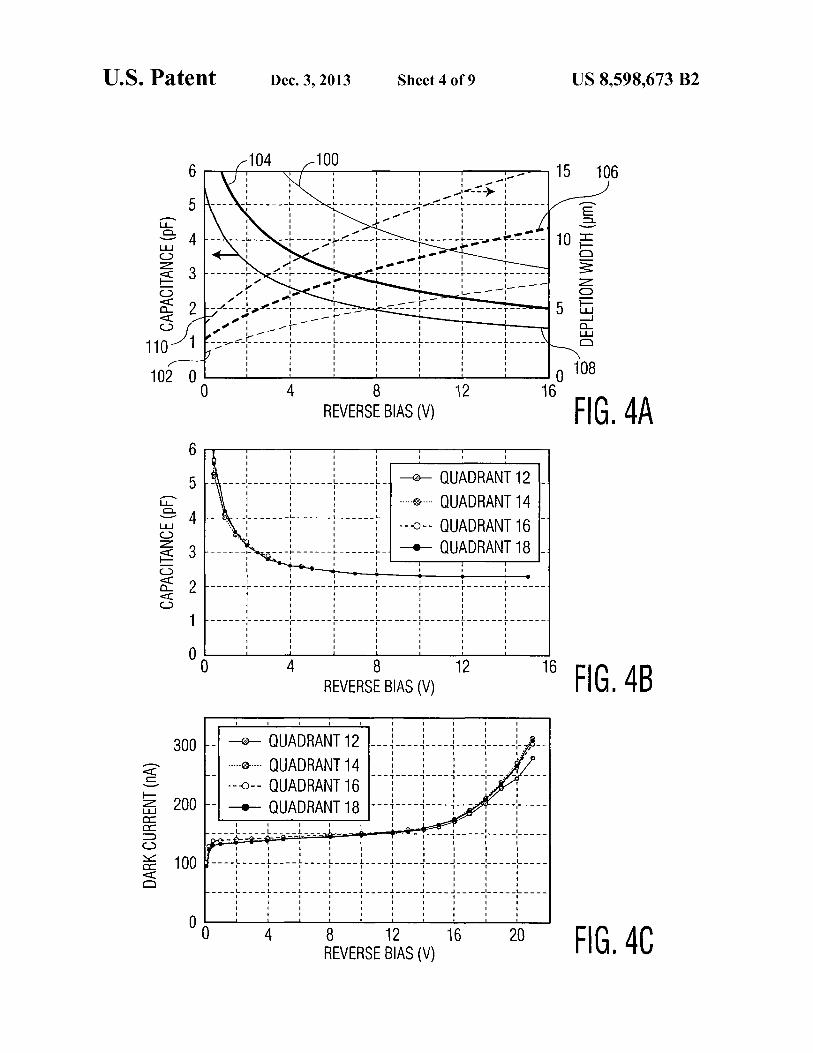
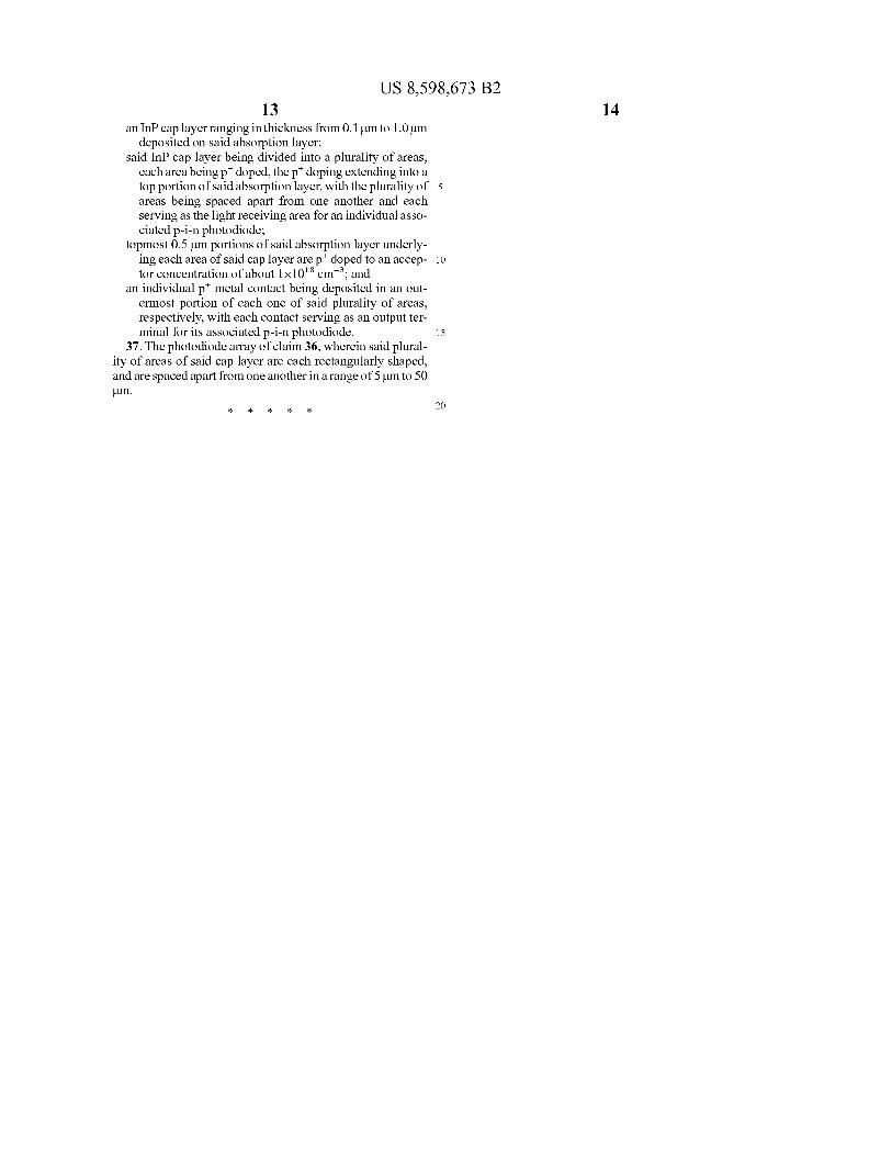
It is also necessary to maintain a low unintentional back-ground doping level to ensure that this intrinsic or depletion region F is depleted at a reasonable photodiode bias. Refer-ring to FIG. 4A, the plot demonstrates that a depletion width F of 9.2 µm can be achieved at 5-V reverse bias for an n-type background doping concentration of 1x10¹⁴ CM-3. Such a depletion width F will result in 2.4-pF capacitance per quad-rant (C D) in a 1-mm diameter quad photodiode. Achieving the same depletion width F at elevated levels of background doping will require higher reverse bias voltage . Also, with further reference to FIG. 4A, curve 100 shows capacitance for one quadrant of photodiode 60 for background doping of 5x10 14 CM 3 ; curve 102 depletion width for one quadrant of photodiode 60 for background doping of 5x10¹⁴ CM-3; curve 104 shows capacitance for one quadrant of photodiode 60 for background doping of 2x10 14 CM 3 ; curve 106 shows deple-tion width for one quadrant of photodiode 60 for background doping of 2x10 14 CM 3 ; curve 108 shows capacitance for one quadrant of photodiode 60 for background doping of 1 x10 14 CM-
3 ; and curve 110 shows depletion width for one quadrant of photodiode 60 for background doping of 1 x10¹⁴ CM
-3 .
Referring to FIG. 413, the quad photodiode reported here had (CD2.5 pF at 5-V reverse bias, therefore implying an n-type background doping of —1 x10¹⁴ CM
-
3 in the intrinsic region. Referring to FIG. 4C, each photodiode quadrant dem-onstrated a dark current, IDARK 140 nA at 5 V reverse bias. Such dark current leads to a shot noise density of 0.2 pA/ -VHz, which is negligible as compared to other noise sources dis-cussed below.
The equivalent input current noise density I, ,FQ of the quad
photodiode 50 in each quadrant 12, 14 , 16, 18 , as shown in FIG. 2, arises from a combination of the voltage noise and current noise of the OpAmp 47, thermal noise from the series resistance of the photodiode 50, thermal noise from the feed-back resistance Rf,B , and shot noise due to the dark current of the photodiode 50. These noise sources are statistically inde-pendent and combine in quadrature and represented by Equa-tion (I) as follows:
NA~ 1 I
~I~ V 2 \ +4n2f 2(Cy~ +CAMy )2 +INA +
INEQU) = RFa
2 4kB T [4gf (Cyr + CAMr) kBTRrD ] + F-e R + 2 DARK
where T is the absolute temperature, kB is the Boltzman's constant, and q is the charge of an electron (see FIG. 1C for other definitions). FIG. 5A displays these noise components and the resulting Ir FQ
for CD2. 5 pF. The values of the other parameters used in these calculations have been given above. The equivalent noise for C D-20 pF is also given in FIG. 5B for comparison. It is evident that IrFQ is limited by the ther-mal noise from the feedback resistor RFB at low frequencies

US 8,598,673 B2 7
8 (Ir,EQ-0.6 pA/-VHz for R,,-5 I kQ at 300 K). At high frequen- FIGS. 8A and 8B show another embodiment of the inven- cies, Ir,EQ is dominated by the input voltage noise of the tion for an array of large area low capacitance photodiodes. OpAmp 47 with CPS+CAm, as the load. Therefore, reduction
Except for the p+ Zn diffusion doping of cap layer areas 116
in the capacitance of the quad photodiodes 50 leads to lower extending into absorption layer 34, the n+ metal back contact noise in the quad photoreceiver 10. Comparison of the noise 5 (common cathode) 20, buffer layer 38, drift layer 36 and of the photoreceiver 10 with the shot noise for 100-µW LO
absorption layer 34 are substantially the same as described
power and 0.9 A/W photodiode 50 responsivity further dem- above for other embodiments of the present invention. In this onstrates the relevance of low-capacitance quad photodiodes embodiment, the photodiode array 112 is arranged to provide 50 (see FIGS. 5A and 513). S rows and T columns of large area low capacitance photo-
Referring to FIG. 6A, owing to the 51-k-Q feedback resis- io diodes 118 each having a p+ metal contact 114 (anode con- tance R,, and the measured photodiode 50 responsivity of 0.9
nection), and a square, rectangular, or circular p+ doped area
A/W at 1550-mu wavelength, for each photoreceiver quad- 116 extending into the absorption layer 34 by about 0.5 µm. rant 12, 14, 16, 18 demonstrated a conversion gain of 45
Although nine photodiodes are shown for purposes of illus-
kV/W with a 3-dB bandwidth of —20 MHz. The —0.5-dB
tration, the array 112 can have up to a practical limit S times discrepancy between the conversion gains of the four quad- 15 T such photodiodes 118. Note that for each photodiode space rants 12, 14, 16, and 18 can be attributed to the device-to- B can range in length from 5 µm to 50 µm, and the sides of device variations in the parameters of the OpAmp 47. Refer- each ifrectangular can range in length from 0. 1 mm to 10 mm, ring to FIG. 613, all photoreceiver quadrants 12, 14, 16, 18
or if circular can range in diameter from 0.1 mm to 10 mm.
demonstrated an equivalent input current noise density of
With reference to FIGS. 3A and 313, a single photodiode <3.2 pA/-VHz up to 20-MHz frequency. The frequency depen- 20 can be obtained through producing a single quadrant 12, 14, dence of the photoreceiver noise confirms the dominance of
16 or 18. The geometry of the p+ doped cap layer 28 portion
the voltage noise contribution of the OpAmp 47. For a
64 and underlying p+ doped absorption layer 34 portion 35 CAS 1.4 pF used in this work, the quad photodiode 44 with
can be other than pie shaped. For example, the p+ doped areas
C,D 2.5 pF allows a 14.5-dB improvement in sensitivity over
64 and 35 can be circular, square, rectangular and other a quad photodiode 50 having 20-pF capacitance per quadrant. 25 shapes. This improvement can increase up to 17 dB as the input
The foregoing discussion discloses and describes merely
capacitance of the OpAmp 47 is further reduced to <0.5 pF. exemplary embodiments ofthe present invention. One skilled Applicants have demonstrated a 1-mm-diameter quad
in the art will readily recognize from such discussion, and
InGaAs photodiode having 2.5-pF capacitance per quadrant
from the accompanying drawings and claims, that various at 5-V reverse bias. This performance was enabled by the 30 changes, modifications and variations can be made therein DDR photodiode structure 62. This quad photodiode array 60
without departing from the spirit and scope of the invention as
was leveraged to develop a quad photoreceiver having an
defined in the following claims. For example, the shape of the equivalent input current noise density of <3.2 pA/ -VHz per quad photodiode array 60 can be other than circular, such as quadrant up to a 3-dB bandwidth of 20 MHz. With reference square, rectangular, and so forth, for example. Also, the to FIG. 7, a plot is shown from test results for measured excess 35 present low capacitance quad photodiode array 60 can be equivalent noise for one quadrant of a 1 mm diameter quad
individually provided for use in applications other than pho-
photoreceiver (see FIGS. 1, 2, 3A and 313) based on an toreceivers. Also, the inventive photodiode structure pre- EL5131 operational amplifier. The solid black curve shows sented herein can be modified to provide either individual low the theoretical simulation, whereas the open small circles capacitance p-i-n photodiodes, or an array of such photo- show the actual measured results. 4o diodes. In addition, one such photodiode can be used to drive
Applicants also used the quad photodiode 60 of FIG. 3B in a single TIA for providing an improved photoreceiver relative combination with a low noise bipolar input operational ampli- to the prior art. Also, the Applicants recognize, as shown fier part number EL5131, manufactured by Intersil of Milpi- above, that the present low capacitance photodiode or photo- tas, Calif. Quad photodiode 60 was used to drive the EL5131
diode array can be utilized for high speed applications, such
operational amplifier having the same equivalent circuit as 45 as free-space communication systems. shown in FIG. 2. In laboratory tests the EL5131 OpAmp resulted in a PIN-TIA excess equivalent input noise of less
What is claimed is:
than 1.6 pA/-VHz over a frequency range of up to 20 MHz. The
1. A large-area low-noise quad photoreceiver comprising: resultant noise versus frequency curve is shown in FIG. 7. a quad InGaAs photodiode structure including: Other embodiments can include integrated TIA chips, TIAs 50 an n+ doped InP substrate having top and bottom sur- based on discrete transistors, and any combination of the
faces;
above. Applicants urge that there are many other uses for the a buffer layer provided by n+ doped InP material depos- low capacitance photodiode as presented herein, whether as a
ited on the top of said substrate for reducing the
single present photodiode, or an array of the present photo- capacitance to enhance the speed of said photodiode; diodes, such as the quad example described above. 55 an n+ metal back contact deposited on the bottom of said
The present invention also includes a number of other substrate, said contact serving as a common cathode embodiments in addition to a quad InGaAs photodiode
for receiving a bias voltage;
coupled to quad TIAs for providing a quad photoreceiver. an intrinsic (i) InP drift layer deposited on the top of said Other embodiments include a low capacitance p-i-n photo- buffer layer; diode alone as described above, and an array of two or more 60 an InGaAs absorption layer deposited on the i InP drift of such photodiodes. In addition, still other embodiments
layer, said drift layer and said absorption layer pro-
include the use of a p-i-n photodiode as described above for viding low-capacitance high-speed operation; driving one TIA to provide an improved photoreceiver. Also, InP cap layer deposited on said absorption layer; as previously noted, the present inventive photodiode may said InP cap layer being divided into four quadrants of have use in other applications than described herein requiring 65 equal area, each quadrant being p+ doped, the p+ dop- such a low capacitance photodiode for improved or enhanced
ing extending into a top portion of said absorption
operation. layer, with the four quadrants being spaced apart from
US 8,598,673 B2 9
one another and each serving as the light receiving area for an individual associated p-i-n photodiode;
an individual p' metal contact being deposited in an outermost portion of each one of said four quadrants, respectively, with each contact serving as an output terminal for its associated p-i-n photodiode; and
four transimpedance amplifiers (TIA) each having an indi- vidual input terminal electrically connected to an output terminal of an individual one of said p-i-n photodiodes, and each TIA having an individual output terminal.
2. The quad photoreceiver of claim 1, further including an anti-reflection coating on said cap layerbetween saidp' metal contacts.
3. The quad photoreceiver of claim 2, wherein said anti-reflection coating consists of silicon nitride.
4. The quad photoreceiver of claim 1, wherein said p' doped quadrants of said cap layer are doped via p+ Zn diffu-sion.
5. The quad photoreceiver of claim 4, wherein the p+ doped Zn diffusion of each quadrant of said cap layer extends 0.5 µm into a top portion of said absorption layer.
6. The quad photoreceiver of claim 1, wherein: said drift layer ranges in thickness from 1.0 µm to 10 µm; said absorption layer ranges in thickness from 1µm to 3
µm; and said cap layer ranges in thickness from 0.1 µm to 1.0 µm. 7. The quad photoreceiver of claim 1, wherein each of said
four quadrants of said cap layer are one-quarter pie shaped. 8. The quad photoreceiver of claim 7, wherein said quad
InGaAs photodiode structure has an active area ranging from 0.1 mm to 10 mm in size for receiving a light signal.
9. The quad photoreceiver of claim 8, wherein said quad InGaAs photodiode structure has a separation or space between quadrants ranging from 5 µm to 50 µm.
10. The quad photoreceiver of claim 1, wherein topmost 0.5 µm portions of said absorption layer underlying said quadrant of said cap layer are p-doped to an acceptor concen-tration of about 1x10¹⁸ CM
-3 .
11. A large-area low-noise quad photoreceiver comprising: a quad InGaAs photodiode structure including:
an n+ doped InP substrate having top and bottom sur-faces;
an n+ doped InP buffer layer deposited on the top of said substrate for reducing the capacitance to enhance the speed of said photodiode;
an n+ metal back contact deposited on the bottom of said substrate, said contact serving as a common cathode for receiving a bias voltage;
an intrinsic (i) InP drift layer ranging in thickness from 1 µm to 10 µm deposited on the top of said buffer layer;
an InGaAs absorption layer ranging in thickness from 1 µm to 3 µm deposited on the i InP drift layer, said drift layer and said absorption layer providing low-capaci-tance high-speed operation;
an InP cap layer ranging in thickness form 0.1 µm to 1 µm deposited on said absorption layer;
said InP cap layer being divided into four quadrants of equal area, each quadrant being p+ doped, the p+ dop-ing extending into a top portion of said absorption layer, with the four quadrants being spaced apart from one another and each serving as the light receiving area for an individual associated p-i-n photodiode;
topmost 0.5 µm portions of said absorption layer under-lying each quadrant of said cap layer are p+ doped to an acceptor concentration of about 1 x10¹⁸ CM-3;
10 an individual p+ metal contact being deposited in an
outermost portion of each one of said four quadrants, respectively, with each contact serving as an output terminal for its associated p-i-n photodiode; and
5 four transimpedance amplifiers (TIA) each having an indi-vidual input terminal electrically connected to an output terminal of an individual one of said p-i-n photodiodes, and each TIA having an individual output terminal.
12. The photoreceiver of claim 11, wherein an uppermost to portion of saidp+ doped cap layer saidphotodiode structure is
circular with a diameter ranging from 0.1 mm to 10 mm, with each one of said from quadrants of said cap layer being one-quarter pie shaped, and spaced apart by 20 µm from one
15 another. 13. A large-area low-capacitance quad photodiode array
comprising: an n+ doped InP substrate having top and bottom surfaces; a buffer layer provided by n+ doped InP material deposited
20 on the top of said substrate for reducing the capacitance to enhance the speed of said photodiode;
an n+ metal back contact deposited on the bottom of said substrate, said contact serving as a common cathode for receiving a bias voltage;
25 an intrinsic (i) InP drift layer deposited on the top of said buffer layer;
an InGaAs absorption layer deposited on the i InP drift layer, said drift layer and said absorption layerproviding low-capacitance high-speed operation;
30 an InP cap layer deposited on said absorption layer; said InP cap layer being divided into four quadrants of
equal area, each quadrant being p+ doped, the p+ doping extending into a top portion of said absorption layer, with the four quadrants being spaced apart from one
35 another and each serving as the light receiving area for an individual associated p-i-n photodiode; and
an individual p+ metal contact being deposited in an out-ermost portion of each one of said four quadrants, respectively, with each contact serving as an output ter-
40 minal for its associated p-i-n photodiode. 14. The quad photodiode array of claim 13, further includ-
ing an anti-reflection coating on said cap layer between said p+ metal contacts.
15. The quad photodiode array of claim 14, wherein said 45 anti-reflection coating consists of silicon nitride.
16. The quad photodiode array of claim 13, wherein said p+ doped quadrants of said cap layer are doped via p+ Zn diffu-sion.
17. The quad photodiode array of claim 16, wherein the p+ 5o doped Zn diffusion of each quadrant of said cap layer extends
0.5 µm into a top portion of said absorption layer. 18. The quad photodiode array of claim 13, wherein: said drift layer ranges in thickness from 1 µm to 10 µm
thick; 55 said absorption layer ranges in thickness from 1.0 µm to 3
µm; and the cap layer ranges in thickness from 0.1 µm to 1 µm. 19. The quad photodiode array of claim 13, wherein each of
said four quadrants of said cap layer are one-quarter pie 60 shaped.
20. The quad photodiode array of claim 19, wherein said quad InGaAs photodiode structure has an active area ranging from 0.1 mm to 10 mm for receiving a light signal.
21. The photodiode array of claim 20, wherein said InGaAs 65 photodiode structure has a separation or space between said
plurality of areas of said cap layer ranging from 5 µm to 50 µm.

US 8,598,673 B2 11
22. The quad photodiode array of claim 20, wherein said quad InGaAs photodiode structure has a separation or space between quadrants ranging from 5 M to 50 µm.
23. The quad photodiode array of claim 13, wherein top-most 0.5 µm portions of said absorption layer underlying said quadrant of said cap layer are p-doped to an acceptor concen-tration of about 1x10 18 CM 3 .
24. A large-area low-capacitance quad photodiode array comprising:
an n' doped InP substrate having top and bottom surfaces; an n' doped InP buffer layer deposited on the top of said
substrate for reducing the capacitance to enhance the speed of said photodiode;
an n' metal back contact deposited on the bottom of said substrate, said contact serving as a common cathode for receiving a bias voltage;
an intrinsic (i) InP drift layer ranging in thickness from 1 µm to 10 µm deposited on the top of said buffer layer;
an InGaAs absorption layerranging in thickness from 1 µm to 3 µm deposited on the i InP drift layer, said drift layer and said absorption layer providing low-capacitance high-speed operation;
an InP cap layer ranging in thickness form 0.1 µm to 1 µm deposited on said absorption layer;
said InP cap layer being divided into four quadrants of equal area, each quadrant being p' doped, the p' doping extending into a top portion of said absorption layer, with the four quadrants being spaced apart from one another and each serving as the light receiving area for an individual associated p-i-n photodiode;
topmost 0.5 µm portions of said absorption layer underly-ing each quadrant of said cap layer are p' doped to an acceptor concentration of about 1x10¹⁸ CM-3 ; and
an individual p' metal contact being deposited in an out-ermost portion of each one of said four quadrants, respectively, with each contact serving as an output ter-minal for its associated p-i-n photodiode.
25. The photodiode array of claim 24, wherein said cap layer is circular with a diameter ranging from 0.1 mm to 10 mm, with each one of said from quadrants of said cap layer being one-quarter pie shaped, and spaced apart in a range of from 5 µm to 50 µm from one another.
26. A large-area low-capacitance p-i-n photodiode com-prising:
an n' doped InP substrate having top and bottom surfaces; an n' doped InP buffer layer deposited on the top of said
substrate for reducing the capacitance to enhance the speed of said photodiode;
an n' metal back contact deposited on the bottom of said substrate, said contact serving as a common cathode for receiving a bias voltage;
an intrinsic (i) InP drift layer ranging in thickness from 1 µm to 10 µm deposited on the top of said buffer layer;
an InGaAs absorption layerranging in thickness from 1 µm to 3 µm deposited on the i InP drift layer, said drift layer and said absorption layer providing low-capacitance high-speed operation;
an InP cap layer ranging in thickness from 0.1 µm to 1.0 µm deposited on said absorption layer;
said InP cap layer being p' doped, the p' doping extending into a top portion of said absorption layer, with said cap layer serving as the light receiving area ranging from 0.008 mm2 to 100 mm2 ;
a topmost 0.5 µm portion of said absorption layer underly-ing said cap layer are p' doped to an acceptor concen-tration of about 1x10¹⁸ CM-3 ; and
12 an individual p' metal contact being deposited in an out-
ermost portion of said cap layer serving as an output terminal.
27. The photodiode of claim 26, wherein said cap layer is 5 circular.
28. A large-area low-capacitance photodiode array com-prising:
an n' doped InP substrate having top and bottom surfaces; an n' doped InP buffer layer deposited on the top of said
l0 substrate for reducing the capacitance to enhance the speed of said photodiode;
an n' metal back contact deposited on the bottom of said substrate, said contact serving as a common cathode for
15 receiving a bias voltage; an intrinsic (i) InP drift layer deposited on said buffer layer; an InGaAs absorption layer deposited on the i InP drift
layer, said drift layer and said absorption layerproviding low-capacitance high-speed operation;
20 an InP cap layer deposited on said absorption layer; said InP cap layer being divided into a plurality of areas,
each area being p' doped, the p' doping extending into a top portion of said absorption layer, with the plurality of areas being spaced apart from one another and each
25 serving as the light receiving area for an individual asso- ciated p-i-n photodiode; and
an individual p' metal contact being deposited in an out-ermost portion of each one of said plurality of areas, respectively, with each contact serving as an output ter-
30 minal for its associated p-i-n photodiode. 29. The photodiode array of claim 28, further including an
anti-reflection coating on said cap layerbetween said p' metal contacts.
30. The photodiode array of claim 29, wherein said anti-35 reflection coaxing consists of silicon nitride.
31. The photodiode array of claim 28, wherein said p' doped plurality of areas of said cap layer are each doped via p' Zn diffusion.
32. The photodiode array of claim 31, wherein the p' doped 40 Zn diffusion of each area of said cap layer extends 0.5 µm into
a top portion of said absorption layer. 33. The photodiode array of claim 28, wherein: said drift layer ranges in thickness from 1 µm to 10 µm
thick; 45 said absorption layer ranges in thickness from 1.0 µm to 3
µm; and the cap layer ranges in thickness from 0.1 µm to 1 µm. 34. The photodiode array of claim 28, wherein each of said
plurality of areas of said cap layer are rectangular. 50 35. The photodiode array of claim 28, wherein topmost 0.5
µm portions of said absorption layer underlying said plurality of areas of said cap layer are p-doped to an acceptor concen-tration of about 1 x10¹⁸ CM
-3 .
36. A large-area low-capacitance photodiode array com-55 prising:
a buffer layer provided by n' doped InP substrate having top and bottom surfaces for reducing the capacitance to enhance the speed of said photodiode;
an n' metal back contact deposited on the bottom of said 60 substrate, said contact serving as a common cathode for
receiving a bias voltage; an intrinsic (i) InP drift layer ranging in thickness from 1
µm to 10 µm deposited on the top of said buffer layer; an InGaAs absorption layer ranging in thickness from 1 µm
65 to 3 µm deposited on the i InP drift layer, said drift layer and said absorption layer providing low-capacitance high-speed operation;
US 8,598,673 B2 13 14
an InP cap layer ranging in thickness from 0.1 µm to 1.0µm deposited on said absorption layer;
said InP cap layer being divided into a plurality of areas, each area being p' doped, the p' doping extending into a top portion of said absorption layer, with the plurality of 5
areas being spaced apart from one another and each serving as the light receiving area for an individual asso-ciated p-i-n photodiode;
topmost 0.5 µm portions of said absorption layer underly-ing each area of said cap layer are p' doped to an accep- io for concentration of about IxIOi$ CM-3 ; and
an individual p' metal contact being deposited in an out- ermost portion of each one of said plurality of areas, respectively, with each contact serving as an output ter- minal for its associated p-i-n photodiode. 15
37. The photodiode array of claim 36, wherein said plural-ity of areas of said cap layer are each rectangularly shaped, and are spaced apart from one another in a range of 5 µm to 50 µm.
* * * * * 20