Updateable 3D Display Using Large Area Photofractive ... · Updateable 3D Display Using Large Area...
39
AFRL-OSR-VA-TR-2013-0199 Updateable 3D Display Using Large Area Photofractive Polymer Devics Pierre Alexandre Blanche TIPD LLC April 2013 Final Report DISTRIBUTION A: Approved for public release. AIR FORCE RESEARCH LABORATORY AF OFFICE OF SCIENTIFIC RESEARCH (AFOSR) ARLINGTON, VIRGINIA 22203 AIR FORCE MATERIEL COMMAND
Transcript of Updateable 3D Display Using Large Area Photofractive ... · Updateable 3D Display Using Large Area...

AFRL-OSR-VA-TR-2013-0199
Updateable 3D Display Using Large Area Photofractive Polymer Devics
Pierre Alexandre Blanche TIPD LLC
April 2013 Final Report
DISTRIBUTION A: Approved for public release.
AIR FORCE RESEARCH LABORATORY AF OFFICE OF SCIENTIFIC RESEARCH (AFOSR)
ARLINGTON, VIRGINIA 22203 AIR FORCE MATERIEL COMMAND

Standard Form 298 (Rev. 8/98)
REPORT DOCUMENTATION PAGE
Prescribed by ANSI Std. Z39.18
Form Approved OMB No. 0704-0188
The public reporting burden for this collection of information is estimated to average 1 hour per response, including the time for reviewing instructions, searching existing data sources, gathering and maintaining the data needed, and completing and reviewing the collection of information. Send comments regarding this burden estimate or any other aspect of this collection of information, including suggestions for reducing the burden, to Department of Defense, Washington Headquarters Services, Directorate for Information Operations and Reports (0704-0188), 1215 Jefferson Davis Highway, Suite 1204, Arlington, VA 22202-4302. Respondents should be aware that notwithstanding any other provision of law, no person shall be subject to any penalty for failing to comply with a collection of information if it does not display a currently valid OMB control number. PLEASE DO NOT RETURN YOUR FORM TO THE ABOVE ADDRESS. 1. REPORT DATE (DD-MM-YYYY) 2. REPORT TYPE 3. DATES COVERED (From - To)
4. TITLE AND SUBTITLE 5a. CONTRACT NUMBER
5b. GRANT NUMBER
5c. PROGRAM ELEMENT NUMBER
5d. PROJECT NUMBER
5e. TASK NUMBER
5f. WORK UNIT NUMBER
6. AUTHOR(S)
7. PERFORMING ORGANIZATION NAME(S) AND ADDRESS(ES) 8. PERFORMING ORGANIZATION REPORT NUMBER
9. SPONSORING/MONITORING AGENCY NAME(S) AND ADDRESS(ES) 10. SPONSOR/MONITOR'S ACRONYM(S)
11. SPONSOR/MONITOR'S REPORT NUMBER(S)
12. DISTRIBUTION/AVAILABILITY STATEMENT
13. SUPPLEMENTARY NOTES
14. ABSTRACT
15. SUBJECT TERMS
16. SECURITY CLASSIFICATION OF: a. REPORT b. ABSTRACT c. THIS PAGE
17. LIMITATION OF ABSTRACT
18. NUMBER OF PAGES
19a. NAME OF RESPONSIBLE PERSON
19b. TELEPHONE NUMBER (Include area code)
14-02-2013 Final Report Nov 2009 - Nov 2012
Updateable 3D Display Using Large Area Photorefractive Polymer Devices FA9550-10-C-0009
Blanche, Pierre-Alexandre
TIPD, LLC1430 N. 6th Ave.Tucson, AZ 85705-6644
USAF, AFRLAF Office of Scientific Research875 N. Randolph St. Room 3112Arlington VA 22203
Distribution Statement A. Approved for public release; distribution is unlimited.
The overall goal of this program was to develop a large area updateable 3D color display using unique and innovativephotorefractive (PR) polymers with fast writing times (ms), long persistence (hours) and rapid erasure (several seconds).A multi-pronged approach was used to integrate the presently established materials, find new photorefractive materials, andelectronics and photonics techniques to achieve the following goals:- 3D display devices: we developed large area PR polymer devices for updateable 3D display.- Materials optimization: we designed and synthesized a PR polymer with high figures of merit for 3D display applications.- Nanosecond pulse recording: recording setups based on a high repetition rate nanosecond pulsed laser to increase the recordingspeed were developed.- Color holograms: A color 3D display system was implemented by angular multiplexing.
holography, photorefractive polymers, 3D display, large area displays, 3D visualization, 3D rendering, dye-doped polymers
U U U SAR 38
Charles Lee
(703) 696-7779
AFRL-OSR-VA-TR-2013-0199

FA9550-10-C-0009
Page 2
Updateable 3D Display Using Large Area
Photorefractive Polymer Devices
FINAL REPORT
Contract No. FA9550-10-C-0009
USAF, AFRL
AF Office of Scientific Research
875 N. Randolph St. Room 3112
Arlington VA 22203
Name of Contractor: TIPD, LLC
Principal Investigator: Dr. Arkady Bablumyan
Business Address: 1430 N. 6th Ave. Tucson, Arizona 85705-6644
Phone Number: (520) 626-7934
Effective Date of Contract: 2009/11/15
Short Title of Work: Updateable 3D Display
Contract Expiration Date: 2012/11/14
Reporting Period: 2009/11/15 – 2012/11/14
Distribution Statement A. Approved for public release, distribution is unlimited.

FA9550-10-C-0009
Page 3
Completion Report
Abstract: The overall goal of this program was to develop a large area updateable 3D color display using unique and innovative photorefractive (PR) polymers with fast writing times (ms), long persistence (hours) and rapid erasure (several seconds).
The motivation behind developing a 3D display is that 2D images lacking parallax and depth give only limited information about an object or a scene. A dynamic 3-D holographic display is potentially very useful for command and control applications like battlefield surveillance especially in complex urban environments. The large-area display enables command personnel to efficiently monitor changes in 3D and in real time, greatly increasing situational awareness, improving response time, and reducing erroneous targeting, among other benefits.
In a first Nature article published in Feb 7, 2008, the University of Arizona team demonstrated for the first time that PR polymers may be employed for a 3D display with image persistence of a few hours. The present effort sought to explore materials and techniques to enable a 300 mm × 300 mm display area, full color, long term persistence, and wide viewing angle holographic 3D display system. A multi-pronged approach was used to integrate the presently established materials, find new photorefractive materials, and electronics and photonics techniques to achieve the following goals:
3D display devices: we developed large area PR polymer devices for updateable 3D display.
Materials optimization: we designed and synthesized a PR polymer with high figures of merit for 3D display applications.
Nanosecond pulse recording: recording setups based on a high repetition rate nanosecond pulsed laser to increase the recording speed were developed.
Color holograms: A color 3D display system was implemented by angular multiplexing.
TECHNICAL REPORT
Objectives
The primary objective of this program was to improve our refreshable holographic 3D display technology by enlarging the screen size (up to 1ft x 1 ft), being able to record full parallax and/or full color holograms, and decreasing the writing time from minutes to seconds. We used a multidisciplinary approach to overcome the various challenges towards achieving this new system. Material development and chemical engineering were used to develop a highly sensitive and efficient photorefractive polymer with transparency over the entire visible spectrum. Optical and mechanical system development were used to improve the holographic recording setup and process in order to include three independent object beams for the three fundamental colors, and to establish a recording system using a nanosecond pulsed laser light

FA9550-10-C-0009
Page 4
source. The specific technical objectives to be fulfilled by TIPD, LLC during this Phase II effort are as follows:
Objective 1. Large area hologram - The proposer may accomplish the following performance goals with respect to a large area hologram:
12” x 12” size
Angle of view > 30°
Resolution: 0.8 mm hogel size
Horizontal parallax only
Monochrome hologram
Objective 2. Full color hologram: - The proposer may accomplish the following performance goals with respect to a full color hologram:
6” x 6” size
Angle of view > 30°
Resolution: 0.8 mm hogel size
Horizontal parallax only
Objective 3. Nanosecond pulse recording – The proposer may accomplish the following performance goals with respect to nanosecond pulse recording:
12” x 12” size
Angle of view > 15°
Resolution: 1 mm hogel size
100 Hz repetition rate
Horizontal parallax only
Monochrome hologram
Objective 4. Full parallax – The proposer may accomplish the following performance goals with respect to full parallax operation:
CW demonstration on 4” x 4” sample
Angle of view > 15°
Resolution: 0.8 mm hogel size
Monochrome hologram

FA9550-10-C-0009
Page 5
Technical Progress
Objective 1. Large area hologram
The generation of large area holograms requires 2 key elements: large photorefractive devices, and the ability to print the entire surface, which is enabled by the optical setup.
1.1. Large PR device Photorefractive devices as large as 12x12 inches in size has been manufactured and proven functional. The following is the general procedure of fabrication for those large area device.
ITO glass substrate preparation
Buffer layer (APC) coating
Composite mixing process
Composite coating on substrate
Vacuum laminating process
The initial manufacturing method of PR devices was labor intensive and requires a knowledgable operator to ensure both homogeneity of the layer and absens of defect that can ultimately lead to destruction of the device during operation under high electric field.
During the course of this program, we refine the manufacture process of large PR device and took the operator skill out of the equation by replacing the manual labor by precisely controled mechanical equipment. This allowed us to improve the quality of the manufacturing and, as a further result, increase the size of the device up to 12x12 inches with a high yield of success.
Previously, The PR mixture was thermally melted onto ITO glass plate and pressed manually to achieve the desired thickness. While this approach was efficient for small devices (up to 4x4 inches), large devices needed a more controlled technique. In order to resolve the issues posed by the manual manufacturing, several automated coating techniques were tried to found out that “Powder coating” gave very homogeneous and bubble-free large area samples. Compared to hand-made method and other techniques, the powder method was found to provide much higher quality samples. The procedure is as follows:
A. Mixing compositions Polymer, chromophore, & plasticizer are mixed and dissolve into DCM solvent, followed by C60/PCBM sensitizer solution to make homogenous solution. Simple composition mixing (No solvent) method can not give good PR performance, probably due to insufficient dispersion of sensitizer and chromophore which has tendency to form bimolecular anti-dipole moment chromophore interactions.
B. Solvent removal Concentrating the composition solution by solvent DCM removal, followed by heating vacuum treatment.

FA9550-10-C-0009
Page 6
Figure 1: Sample preparation: filtration / solvant removal / miling.
C. Milling After cooling down the residue, the reside is milled into fine powder, followed by further drying.
D. Spreading By homogenous spreading the composition powder onto ITO substrate with around 1mm thickness, the sample is then heated, melted, and vacuumed to remove bubbles.
E. Assembly One pair of pre-coated samples (thickness around 100um) were sandwiched under heating vacuum to provide very homogeneous thickness appearance fabricated sample.
Figure 2: Sample preparation: Spreading /Heating and assembly.
Figure 3: The vacuum lamination machine. Fully automated, this machine is able to laminate samples up to 1ft x 1ft under vacuum without generating any air bubbles.
hheeaatteerrss
LLaammiinnaattiinngg::
TToopp mmoovviinngg ddoowwnn

FA9550-10-C-0009
Page 7
Numerous functional PR device have been produced by this technique of powder pre-melding and vacuum lamination. A very high yield on the device has been achieved, and only few sample have had to be rejected due to impurities. Figue 4 show a 12x12 device ready for holographic recording.
Holographic setup The second part of the creating large hologram is to develop an optical printer setup capable of recording such large size holograms. We extended the display size to as large as 12x12". After NDT had acquired the capability to produce photorefractive devices up to 12x12", we adapted the recording setup to accommodate those large devices. The major issue was the lack of commercially available optics, especially cylindrical lenses, large enough to generate hogels 12 inches tall. To go around that problem, we decided to write 12" hologram by two passes, one writing the bottom of the hologram the second one, writing the top of the hologram. Doing so, we learned valuable information on tiling holograms for future larger screen.
The largest holograms we recorded were 12x12" in size. The vertical size was determined by the height of the cylindrical lens focusing the object beam to the PR device. We did not find readily available 12” cylindrical lens to generate 12” hogel in a single pass. To fulfill this task, we decided to write the hologram by two superposed rows, 6" each, for a total of 12".
Since the recording of the two rows takes twice the time of a single raw, we used the pulsed setup that is fast enough. This way, no noticeable difference appears in the diffraction efficiency between the first recorded and second recorded part of the hologram. The pulsed setup was already be set for two color recording so the 12x12 hologram will also be two colors.
To write the two rows one on the top of the other, we used a translation stage to move the PR device vertically. The stage can be seen on the picture below.
Figure 4: A 12x12 inch PR device.

FA9550-10-C-0009
Page 8
If the two rows are recorded without any modification on the setup, the viewer only see one row at a time and the hologram is not perceived as a whole but as two separated entities. This can be understand using the sketch bellow where one can see that the diffracted light from each row is collimated, and thus only reach the viewer eye when this later is at the correct height.
To compensate for that problem, we put a lens in front of the PR device and now the diffracted beams are focalised (no more collimated). So the viewer eye will captures rays of light coming from both the top and bottom row as depicted in the following sketch.
Figure 5: Large hologram recording setup
Figure 6: Sketch of the diffraction by two independent rows. The viewer see only one row at a time.

FA9550-10-C-0009
Page 9
The picture below shows the setup with the observation lens put in front of the PR device
Here are examples of color holograms recorded with the system.
Figure 7: Sketch of the diffraction light focused by a lens. The viewer see the ligth coming from both top and bottom rows at once.
Figure 8: Image of the large area holographic printer with a large spherical lens in front of the PR device.
FA9550-10-C-0009
Page 10
Figure 9: Example of two color large area holograms recorded on 12x12 PR device.
The metrics for the large area holograms are exceeding the objectives proposed for this program. Indeed, the large area holograms have a resolution of 0.5mm per hogels (0.8mm was proposed), they are two color (monochrome was proposed), and the angle of view is larger than 30°.
Objective 2. Full color hologram
There are two main aspects in creating full color hologram. We first have to synthesis a material that will allow blue color to be diffracted. Second, we have to design a holographic recording system that can record three hologram and mix the color toward the viewer direction.
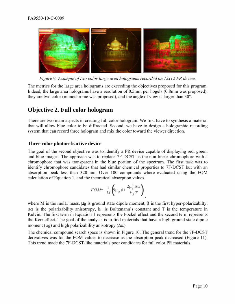
Three color photorefractive device The goal of the second objective was to identify a PR device capable of displaying red, green, and blue images. The approach was to replace 7F-DCST as the non-linear chromophore with a chromophore that was transparent in the blue portion of the spectrum. The first task was to identify chromophore candidates that had similar chemical properties to 7F-DCST but with an absorption peak less than 320 nm. Over 100 compounds where evaluated using the FOM calculation of Equation 1, and the theoretical absorption values.
FOM= 1M (9μ g β+
2μ g2 ∆α
k B T ),
where M is the molar mass, µg is ground state dipole moment, is the first hyper-polarizabilty, is the polarizability anisotropy, kB is Boltzmann’s constant and T is the temperature in Kelvin. The first term in Equation 1 represents the Pockel effect and the second term represents the Kerr effect. The goal of the analysis is to find materials that have a high ground state dipole moment (µg) and high polarizability anisotropy ().
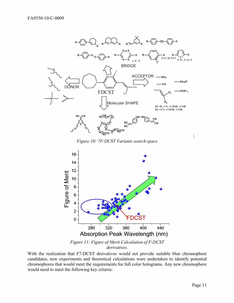
The chemical compound search space is shown in Figure 10. The general trend for the 7F-DCST derivatives was for the FOM values to decrease as the absorption peak decreased (Figure 11). This trend made the 7F-DCST-like materials poor candidates for full color PR materials.
FA9550-10-C-0009
Page 11
With the realization that F7-DCST derivatives would not provide suitable blue chromophore candidates, new experiments and theoretical calculations were undertaken to identify potential chromophores that would meet the requirements for full color holograms. Any new chromophore would need to meet the following key criteria:
| Figure 10: 7F-DCST Variants search space
Figure 11: Figure of Merit Calculation of F-DCST derivatives.

FA9550-10-C-0009
Page 12
Peak absorption wavelength of 420nm or lower in the PR material. This film wavelength translated to a peak absorption of 370nm or lower in solution
FOM calculated by Equation 1 greater than or equal to 6
Good phase stability either with a single chromophore or a mixture of chromophores.
The FOM of over 150 candidate chromophores was calculated according to Equation 1. Of those over 30 chromophores had theoretical values of the absorption wavelength and FOM which suggested additional study. The 30 candidate chromophores were synthesized using a process similar to that shown in Figure 12 which outlines the process for assembling BDFDFB.
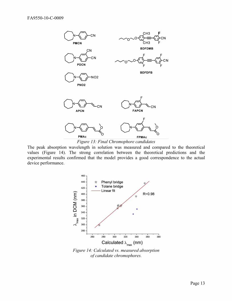
Phase stability testing on the 30 candidate chromophores yield nine (9) chromophores (Figure 13) that had good phase stability and provided good PR performance. Seven of the compounds contained a Phenyl bridge and two of the compounds contained a Tolane bridge.
Figure 12: Synthesis step for assembling BDFDFB
FA9550-10-C-0009
Page 13
The peak absorption wavelength in solution was measured and compared to the theoretical values (Figure 14). The strong correlation between the theoretical predictions and the experimental results confirmed that the model provides a good correspondence to the actual device performance.
Figure 14: Calculated vs. measured absorption of candidate chromophores.
Figure 13: Final Chromophore candidates

FA9550-10-C-0009
Page 14
The figure of merit calculation was validated by comparing the observed n change at 60V/m versus the calculated FOM. The macroscopic n change is related to the FOM described in Equation 1 through the following relation:
Where n is the refractive index change, N is the number of molecules, Wt is the weight of the chromophore used in fabricating the material and MW is the molecular weight. Figure 15 shows the calculated FOM versus n. The strong linear relationship confirms the success of the model in predicting chromophore performance. The key feature of the new phenyl based compounds is that this structure when matched with an inductive acceptor decouples the transparency and the non-linear optical effects. Figure 16 overlays the relationship for the FOM calculated for the new phenyl bridge compounds on 7F-DSCT derivatives. The sharp increase in the slope of the line indicates that the Tolane bridge compounds are able to simultaneously satisfy the absorption and FOM requirements. The Tolane chromophores have a rigid structure and display poor phase compatibility with the other PR components. To improve the phase stability, a mixture of APCN and BDFDFB (3:1) chromophores has been determined to have the best combination of brightness and phase stability. PMMA was chosen as the buffer material due to improved brightness over APC in full color applications. A new image enhancer additive DBA (DiBenzylideneAcetone) with 1-5% loading ratio was identified and optimized for better image performance; although details of the image enhancement mechanism are still unknown. This composition yielded a sensitivity of 5 mJ/cm-2.
Figure 15: Experimental Dn vs. FOM for blue chromophores

FA9550-10-C-0009
Page 15
As it can be seen in figure 17, the material color of the full color composition is considerably lighter (yellow) than for the 2 color device which is amber. When the 2 color composition absorbs the blue diffracted light strongly, the full color material let it get through and the external diffraction efficiency is restored.
Figure 17: a) Full color PR device. b) 2 color PR device.
Three color holographic setup The optical configuration had to be modified for three color operation. The basic configuration remained the same as for monochromatic hologram with reference and object beams interfering to write holographic pixels (figure 18). However, three separate object and reference beam pairs are now included in the system.
Figure 16: Phenyl vs. Tolane based FOM

FA9550-10-C-0009
Page 16
The first two colors were implemented by using a P-polarized object and reference beam for one color and an S-polarized object and reference beam for the second color. The orthogonal polarization prevent the beam to interfere within each other, and no color crosstalk is observed.
To implement a third color, we can not use another polarization since there only exists two independent polarizations. To create a third independent pair, a symmetry in the PR polymer device is exploited: when two beams are incident to the PR device from each side of the normal, and with equal angle, their interference pattern does not generate any index grating in a PR organic material. This is due to the fact that the pattern vector is orthogonal to the applied external electric field, and the generated charges can not be driven by this field in the dark region of the grating.
Accordingly, the angles of the various beams are selected to overlap all three colors in the viewing area while eliminating the appearance of any unwanted diffraction orders in the viewing area. Figure 19 shows how the object beams are polarized and incident to the PR device to record 3 independent holograms that will further diffract the three fundamental colors (red, green, and blue). It has to be noted that the three holograms are recorded in the same space (volume) of the material. There is no spatial color separation like it is the case with 2D displays that use different diode (or filter) to generate the three different colors.
Figure 18: 3D Display optical setup sketch. PBS: polarizing beam splitter; SLM: spatial light modulator; λ/2: half-wave plate; λ/4: quarter-wave plate.

FA9550-10-C-0009
Page 17
When reading the three holograms, the incidence angle of the three light sources are selected such as the Bragg equation is satisfied, including the chromaticity difference since we are recording the hologram at 532 nm and reading them at 633, 532 and 488 nm respectively. The light from the three sources are diffracted independently by its intended grating, and the three diffracted beams are redirected toward the viewer that sees a full color hologram. Figure 20 show picture of full color holograms where one can see the progression achieved during the course of this program, with the early results having three separated colors and some color bleeding, and final result achieving very good color mixing and absence of artifact.
Figure 19: Three color recording setup schematic with beam polarizations.

FA9550-10-C-0009
Page 18
Figure 20: Pictures of full color holograms. a) Early result. b) End of program result.
Considering the proposed metrics for this task of the program, all the objectives have been achieved: we have manufactured PR devices and print full color hologram as large as 6” x 6” in size, the angle of view was superior to 30°, and the resolution was better than 0.8 mm per hogel (0.5 mm achieved).
Objective 3. Nanosecond pulse recording
There are three components to be optimized for nanosecond pulse recording operation: the PR material, the laser light source that will deliver the pulse, and the optical recoding setup where every components need to be integrated and synchronized.
3.1. Material optimization The technical objective of this task is to improve the material properties of the photorefractive polymer to achieve holograms that would be visible in room light when recorded with a nanosecond pulsed laser.
The material composition for pulsed or CW operation is quite different. Indeed even though the average energy is the same for both laser (20 W), the energy delivery from the pulsed laser is composed of a very brief (nanosecond), and very intense (MW) peak. The material needs to be sensitive to that mode of energy.
We identified five key parameters in the optimization of the material:
Speed – how quickly the diffracted signal reaches 50% of its maximum value.
Diffraction efficiency (DE) – how much of the light incident on the diffraction grating is diffracted into the 1st order signal.
Lifetime – how long the photorefractive material could be used before failure.
FA9550-10-C-0009
Page 19
Energy (Sensitivity) – the input laser energy at the plane of the photorefractive material required to generate a visible hologram.
Size – the usable size of the photorefractive film.
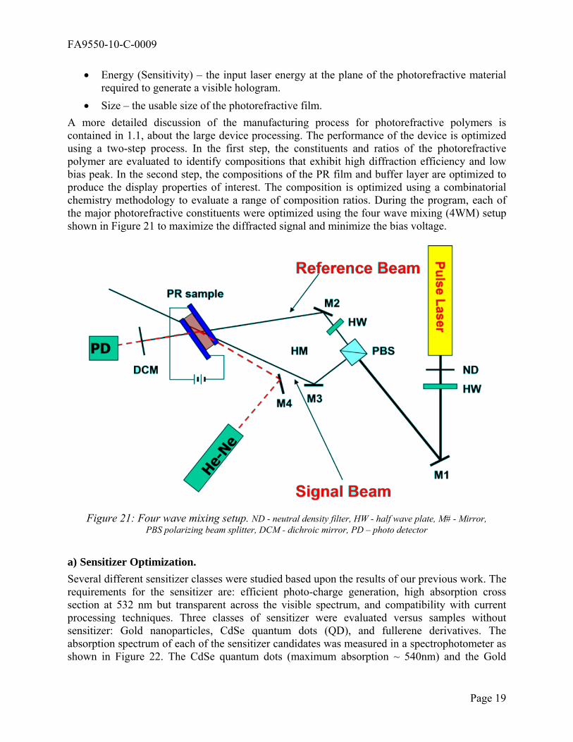
A more detailed discussion of the manufacturing process for photorefractive polymers is contained in 1.1, about the large device processing. The performance of the device is optimized using a two-step process. In the first step, the constituents and ratios of the photorefractive polymer are evaluated to identify compositions that exhibit high diffraction efficiency and low bias peak. In the second step, the compositions of the PR film and buffer layer are optimized to produce the display properties of interest. The composition is optimized using a combinatorial chemistry methodology to evaluate a range of composition ratios. During the program, each of the major photorefractive constituents were optimized using the four wave mixing (4WM) setup shown in Figure 21 to maximize the diffracted signal and minimize the bias voltage.
a) Sensitizer Optimization. Several different sensitizer classes were studied based upon the results of our previous work. The requirements for the sensitizer are: efficient photo-charge generation, high absorption cross section at 532 nm but transparent across the visible spectrum, and compatibility with current processing techniques. Three classes of sensitizer were evaluated versus samples without sensitizer: Gold nanoparticles, CdSe quantum dots (QD), and fullerene derivatives. The absorption spectrum of each of the sensitizer candidates was measured in a spectrophotometer as shown in Figure 22. The CdSe quantum dots (maximum absorption ~ 540nm) and the Gold
Figure 21: Four wave mixing setup. ND - neutral density filter, HW - half wave plate, M# - Mirror, PBS polarizing beam splitter, DCM - dichroic mirror, PD – photo detector

FA9550-10-C-0009
Page 20
nanoparticles (maximum absorption ~510 nm) both demonstrate absorption peaks near the 532nm laser operating frequency and thus may produce reduced intensity in the imaging and 4WM configuration.
Figure 23 shows the CW four-wave mixing response of various sensitizers. PCBM showed the fastest rise time and highest signal level. The CdSe quantum dots and Au nanoparticles experience decrease in sensitivity and were not considered for further study.
Figure 23 shows the improvement in the response for the pulsed laser 4WM configuration.
Figure 22: Absorption Spectra of various sensitizers candidates.
Figure 23: Dynamic response to various sensitizers

FA9550-10-C-0009
Page 21
Fullerenes showed the highest signal level and the fastest rise time in CW operation. Fullerenes also displayed a faster rise time and higher signal than the control sample in pulse operation (figure 24). Based upon the initial data, over 10 different Fullerene derivatives with different fullerene structures and different radicals were evaluated for performance characteristics. The results of the final three candidates are shown in Figure 25 below. [6,6]-Phenyl C61 butyric acid methyl ester (PCBM) was selected as the best sensitizer. Additional studies were completed to determine the optimal concentration of 0.2%.
Figure 25: Performance comparison of various fullerene configurations
b) Chromophore Optimization. The optimization of the NLO chromophore leveraged the previous work with PR materials which indicated that 7-DCST provided good signal level. The metrics used to evaluate the chromophore were high signal level in both pulse and CW operation and good phase stability for long lifetime. The Figure-of-Merit (FOM) shown in Equation 1 was used to evaluate the expected chromophore performance.
Figure 24: Pulse response to PCBM

FA9550-10-C-0009
Page 22
FOM= 1M (9μ g β+
2μ g2 ∆α
k B T ),
where M is the molar mass, µg is ground state dipole moment, is the first hyper-polarizabilty, is the polarizability anisotropy, kB is Boltzmann’s constant and T is the temperature in Kelvin. The first term in Equation 1 represents the Pockel effect and the second term represents the Kerr effect. The goal of the analysis is to find materials that have a high ground state dipole moment (µg) and high polarizability anisotropy (). The semi-empirical FOM calculation was completed using Austin Model 1 (AM1) software1 for geometry optimization, ZINDO2/S-CI to compute the UV-visible absorption, and finite field (FF) analysis to calculate the non-linear optical effect.
At the start of the program, the best performing chromophore was 7-DCST [2-(4-(azepan-1-yl)benzylidene)malononitrile] which provided high diffraction efficiency but showed poor phase stability often separating within a few months. When separating the device turns from transparent to cloudy and can not be used anymore to record hologram. Equation 1 was used to identify several other potential chromophores with similar FOM values. These compounds are shown in Figure 26. Our study indicated that the 7F-DCST was the best chomophores for pulsed operation.
1 Dewar, M. J. S., Zoebisch, E. G., Healy, E. F. and Stewart, J. J. P., Journal of the American Chemical Society, 107, 3902, 1985. 2 M. Zerner, Reviews in Computational Chemistry, 2, Eds. Lipkowitz, K. B. and Boyd, D. B., VCH, New York, 313, (1991)

FA9550-10-C-0009
Page 23
c) Polymer Matrix Optimization The polymer matrix plays three critical roles in the PR material. The first is to provide traps for the photo-generated electrons and holes. These traps create the space charge field that is responsible for orienting the chromophores. The second is to provide rapid transport of the photo-generated electrons and holes to the trap locations under the presence of the bias field. The third is to provide a mechanical “back bone” structure to the photorefractive polymer mixture. The initial CW photorefractive polymer films used Poly(9-vinylcarbazole) (PVK) which provides a high trap density, but electron transport times on the order of a few seconds as shown in Figure 27. For effective pulse operation, faster electron transport times (< 30ms) were needed. Based upon the PVK results, the response time of two copolymers, Carbazole (9H-Carbazole) + DCST and TPD (Tetra-Phenyl Diaminobenzidine) + DCST were investigated. The chemical compositions are shown in Figure 28.
Figure 26: Chromophore candidates

FA9550-10-C-0009
Page 24
Figure 27: Comparison of various PVK matrix polymer compounds for diffraction efficiency and response time
Four-wave mixing experiments indicated that the TPD copolymer provided faster response than either the PVK or Carbazole mixtures. Additional testing indicated that a 10:1 ratio of TPD to
Figure 28: Chemical structure of Carbazole and TPD
FA9550-10-C-0009
Page 25
DCST provided the fastest response time and the smallest solubility parameter mismatch to the 7F-DCST chromophore (SP = 0.35).
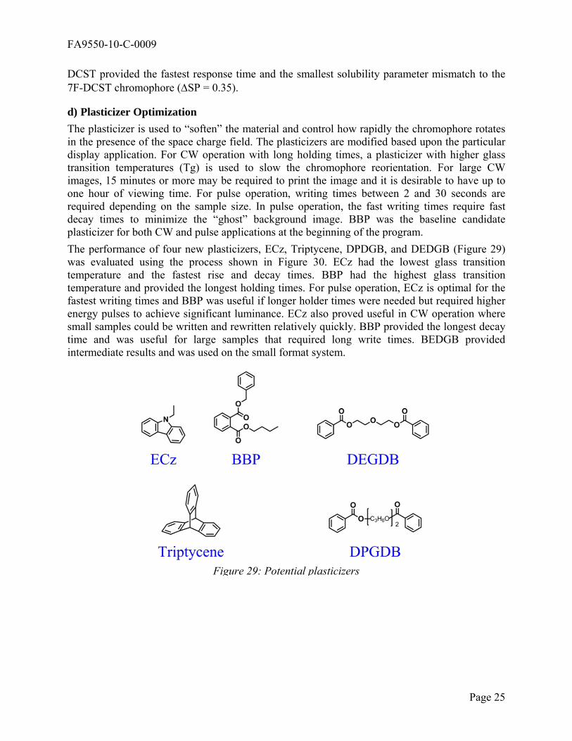
d) Plasticizer Optimization The plasticizer is used to “soften” the material and control how rapidly the chromophore rotates in the presence of the space charge field. The plasticizers are modified based upon the particular display application. For CW operation with long holding times, a plasticizer with higher glass transition temperatures (Tg) is used to slow the chromophore reorientation. For large CW images, 15 minutes or more may be required to print the image and it is desirable to have up to one hour of viewing time. For pulse operation, writing times between 2 and 30 seconds are required depending on the sample size. In pulse operation, the fast writing times require fast decay times to minimize the “ghost” background image. BBP was the baseline candidate plasticizer for both CW and pulse applications at the beginning of the program.
The performance of four new plasticizers, ECz, Triptycene, DPDGB, and DEDGB (Figure 29) was evaluated using the process shown in Figure 30. ECz had the lowest glass transition temperature and the fastest rise and decay times. BBP had the highest glass transition temperature and provided the longest holding times. For pulse operation, ECz is optimal for the fastest writing times and BBP was useful if longer holder times were needed but required higher energy pulses to achieve significant luminance. ECz also proved useful in CW operation where small samples could be written and rewritten relatively quickly. BBP provided the longest decay time and was useful for large samples that required long write times. BEDGB provided intermediate results and was used on the small format system.
Figure 29: Potential plasticizers

FA9550-10-C-0009
Page 26
Figure 30: Plasticizer Evaluation Methodology

FA9550-10-C-0009
Page 27
e) Buffer Layer Optimization. The buffer layer plays a critical role in the device performance. The buffer layer acts as a mechanical interface layer between the “hard” ITO layer and the “soft” PR layer. It also provides a process variable that allows the researcher to tailor the flow of electrons between the electrodes and acts as an insulator to minimize the opportunities for electrical breakdown across the thin PR layer. The critical parameters for the buffer layer are: transparent over the range 400nm to 800nm, high dielectric strength, ease of deposition, and low cost. Five compounds [Polycarbonate, Polystyrene, Poly(methyl methacrylate), Polyarylate, and Polyethersulfone] met the listed criteria and are shown in Figure 31.
The candidate buffer layers were tested to determine maximum signal level and minimum signal peak using the standard PR material composition. The results are shown in Figure 32. The PES buffer layer sample produced a low signal level and the maximum signal level occurred at too high a bias voltage to be able to operate safely. PES was excluded from further evaluation due to its poor performance. The four remaining samples were evaluated for breakdown voltage. The breakdown voltage test involved one-inch samples of the standard PR material with a thickness of 60 µm sandwiched between various buffer layers. The voltage across the PR material is raised in 5V increments until a short is detected by the current monitor ash shown in Figure 33. The voltage value is recorded and the process continues until the next failure. The failure versus bias voltage is analyzed using Weibull analysis3. The Weibull analysis can be used to extrapolate the small sample failure rate to larger samples at the operating voltage. Table 1 summarizes the buffer data analysis.
3 Weibull, W., "A statistical distribution function of wide applicability", J. Appl. Mech.-Trans. ASME 18 (3): 293–297, 1951
Figure 31: Buffer layer candidates

FA9550-10-C-0009
Page 28
APC was chosen as the preferred buffer layer for the PR device based upon its higher signal strength and ease of processing. Additional experiments were conducted to determine if adding an electrolyte solution to the buffer layer would improve performance. Several electrolyte compounds were tested including MPP, TBAT, and 7F-DCST. The best performing electrolyte compound and concentration was 0.5% 7F-DCST which improved the signal level by approximately a factor of two (Figure 34).
Material Operating Voltage
[kV]
Signal Strength
[Arbitrary Units]
Failure rate
@ 300 V/µm
Predicted Failure rate
@ Operating V with 300mm x 300mm sample
APC 3.6 5.7 75% 9 × 10⁻²
PAR 3.6 4.9 95% 5 × 10⁻⁵
Figure 32: Signal Response of various buffer layers
Figure 33: Voltage breakdown experimental setup

FA9550-10-C-0009
Page 29
PMMA 5.3 3.4 75% 2.0 × 10⁻³
PS 6.5 2.4 80% 6.6 × 10⁻¹
Table 1 Summary buffer performance data
3.2. Laser The laser system we used to record the hologram is a pulsed doubled YAG with seeder, emitting 200 mJ per pulse. The intensity lower limit is fixed by the PR device sensitivity while the upper limit is fixed by SLM and PR material damage threshold.
We have successfully used different systems:
Innolas SF Hybrid (pictured here below)
Continuum Powerlite
Continuum Surelite
Figure 34: Comparison of APC (APEC) and APC with 0.5% 7F-DCST buffer

FA9550-10-C-0009
Page 30
The emission wavelength is doubled from the fundamental frequency of 1064 nm to 532nm. This is required by the sensitivity bandwidth of the PR material. The pulse repetition rate has to be slower than the SLM frame refreshing rate (see the recording setup section), both 10Hz and 50Hz laser system have been used. The laser is externally triggered by a computer monitoring the different subsystems of the setup.
The laser system is seeded to increase the coherence length up to 2 meters. Indeed, for the reference beam and object beams to interfere, the coherence length has to be larger than the beam path difference between those beams. The seeder is a laser diode with very precise wavelength that light is directly injected into the laser cavity. Doing so, the seeder impose its own frequency over all the others the laser cavity could emit, and lock the mode for a longer coherence length.
The laser beam profile influences the final hologram image quality. Intra-cavity depolarization and diffraction rings will show as hologram inhomogeneities. In order to homogeneise the laser beam, that can show rings structure, we used a diffuser in the object beam path, just before the SLM. The amount of scattering by the diffuser is critical and will define the resolution at the hologram level. If the dcattering is too small, the ring structure of the laser shows, if it is too large, the resolution is downgraded and the diffuser structure is perceived by the viewer. In order to tune the scattering from the diffuser, we used two ground glass with an index fluid (oil) in between. By carefully selecting the index of the oil, the amount of scattering can be adjusted.
The emitted light from the laser does not need to be polarized since polarized beam splitters are used to separate reference and object beams. Halve wave plates are then used to control the polarization so the interfering beams have the same linear polarization.
We have built a holographic printer based on the different pulsed laser systems. We have addressed the different issue of handling the laser power and the repetition rate speed.
Figure 35: Picture of the Innolas hybrid pulsed laser.

FA9550-10-C-0009
Page 31
As for the laser power, there is no focal point in high power region of the beam path (before the SLM). The spatial light modulator has been certified to operate at the full laser power without optical damage.
Concerning the repetition rate, we have seen limitation in the refreshing rate of the spatial light modulator. Maximum frequency is 60 Hz and can not match the 100Hz of the Innolas laser. If the laser is emiting a pulse when the image is not yet loaded to the SLM, a uncorrect hogel will be recorded into the PR device and the hologram will look funny To ensure this does not happen, the software piloting the experiment has been written so the laser is triggered to the closest pulse following the image upload. The laser frequency can not be arbitrary selected. It has to be a natural divider of the flash lamp repetition rate. In the case of the Innolas system this frequency is 100 Hz, so the closest natural divider is 2 for a frequency of 50 Hz. We have certified that the full experiment can indeed run at a frequency of 50 Hz with an oscilloscope monitoring the flash of laser light.
3D images have successfully been recorded with the pulsed laser system. Recording time has dropped from 3 minutes with the CW laser to 2 seconds with the pulsed system for the same screen size (4x4 inches).
Another advantage of using nanosecond pulse recording laser is that any mechanical vibration is too slow to move the interference fringes during the 6ns of recording time. In effect, the system becomes desensitized from ambient noise (air turbulence, audio noise, ground vibration) and can be operated in industrial environment without any dampening such as floating optical table. This caracteristic is only achieved if the each hogel is recorded with one single pulse. If more pulses are needed per hogel, the subsequent pulses need to be in phase with the first one in order to build up the grating, and the desensitization does not operate anymore.
3.3. Recording setup To move the object and reference writing beams from one hogel position to another on the PR device, a translation stage is used. The PR device can be mounted directly on the stage but the writing and reading locations are different and the viewer see the screen moving which is not convenient. Another solution is to put the optical recording system itself on a translation stage.
The laser head does not need to be mounted on the translation stage since the emitted beam does not have a divergence large enough compared to the translation distance. Though, the unexpanded part of the object and reference beam needs to be parallel to the translation direction. This is to avoid any movement relative to the optics mounted on the translation stage.
Optics mounted on the stage are:
SLM/beam splitter cube assembly
Object beam telescope and last focusing optics
Reference beam telescope and periscope

FA9550-10-C-0009
Page 32
The stage is controlled by the computer monitoring the different subsystems of the setup. Its position and speed vary through the recording process (see sequence of event section).
Different stages have been used successfully during this program:
Newport ILS
Newport IMS
Aerotech PRO165LM
The laser system is a pulsed doubled YAG with seeder, emitting 200 mJ per pulse. The intensity lower limit is fixed by the PR device sensitivity while the upper limit is fixed by SLM and PR material damage threshold. We have successfully used different systems:
Innolas SF Hybrid (pictured here below)
Continuum Powerlite
Continuum Surelite
Figure 36: Optical head on translation stage, picture.
FA9550-10-C-0009
Page 33
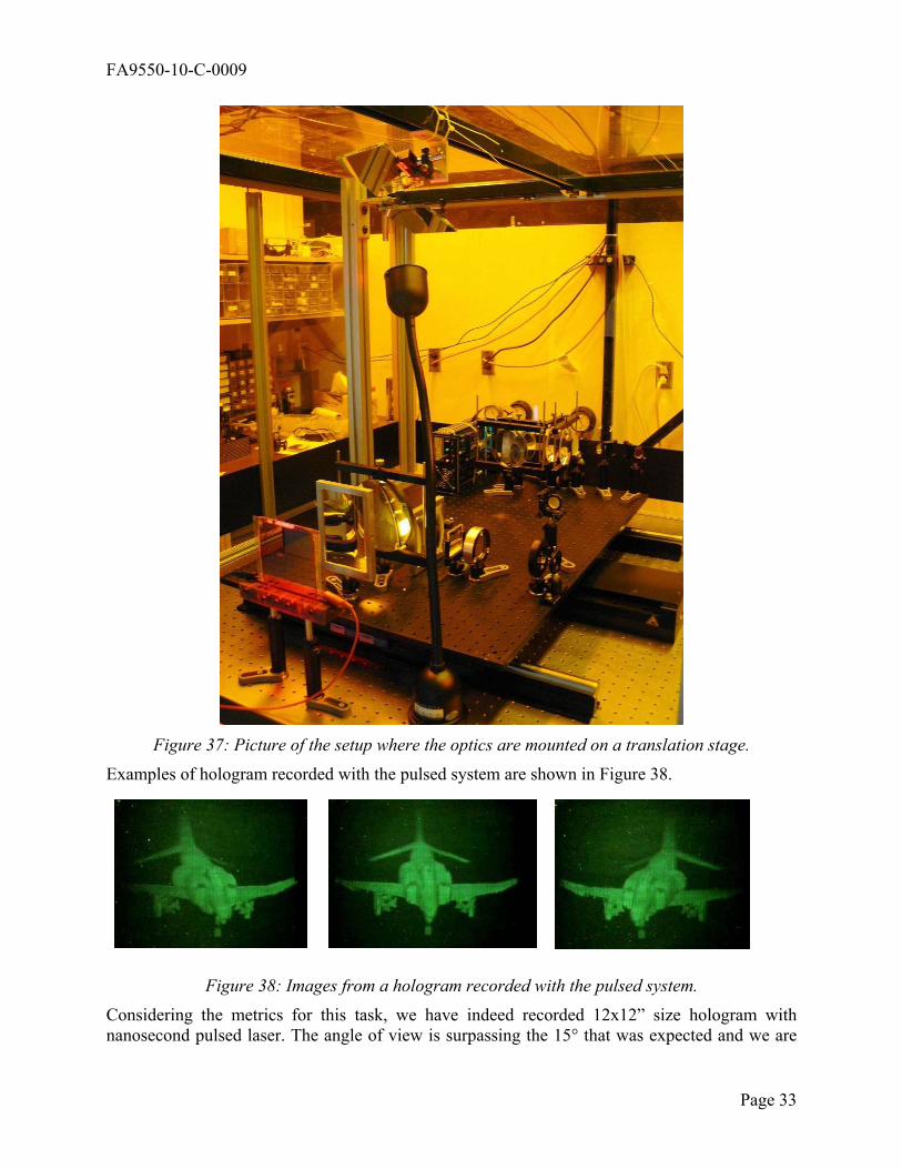
Figure 37: Picture of the setup where the optics are mounted on a translation stage.
Examples of hologram recorded with the pulsed system are shown in Figure 38.
Figure 38: Images from a hologram recorded with the pulsed system.
Considering the metrics for this task, we have indeed recorded 12x12” size hologram with nanosecond pulsed laser. The angle of view is surpassing the 15° that was expected and we are

FA9550-10-C-0009
Page 34
over 30°. The resolution is much better than the 1 mm hogel size, since the hogels are 0.5 mm in the different systems.We have to give up on the repetition rate because of the SLM refresh rate so, we are not operating at 100 Hz, but at 50Hz. We also have demonstrated that we can record two color hologram with this pulsed system when monochromatique hologram were proposed for this task.
Objective 4. Full parallax
This task is about demonstrating a 4x4 inch full parallax 3D display. We know that the difficulty with full parallax is the number of hogels that increase as a square factor compared to the horizontal parallax only. So for a 4x4 inch display which contains 100 hogels in HPO, full parallax will require 100x100=10,000 hogels. With our fastest current system running at 50Hz, it will take 200 seconds to record. This is too long compare to the material persistency time.
Figure 39: Image of a 2 color hologram recorded with nanosecond pulse laser.

FA9550-10-C-0009
Page 35
To overcome this problem we are multiplexing the recording optical system. The reference beam and the object beam were divided into n sub apertures each one writing a different hogel. Since in HPO we are using a slit shaped hogel with a total area of 1cm², we can redistribute that surface (more strictly speaking this energy) in about 100 square shaped hogels with 1mm side. This will decrease the recording time by a factor of 100 and we were able to write a 4x4” full parallax hologram at the same speed as HPO hologram.
Figure 41 show how we use lens arrays to structure the light of the object and reference beam to form several square hogels. The information loaded on the SLM that modulates the object beam is computed according to this geometry so the hologram is intelligible.
Figure 41: Multiplexing the recording system for full parallax.
We have manufactured the holographic optical element that were used in the reference beam as well as the chromium mask to shape the hogels (see Figure 42). The holographic optical element
Figure 40: Horizontal parallax vs full parallax hogels, sketch

FA9550-10-C-0009
Page 36
is constituted of 8x9 square lenses that focus the incident light on the PR devices. The chromium mask is used to define the shape of the hogels and is composed of 7x9 square appertures.
a b
Figure 42: holographic optical element (a), and chromium mask (b), for full parallax writing.
A first test with the continuous wave laser setup has been made on a 2x2” PR device showing good results and validating the concept. We have recorded a full parallax hologram in less than 2 minutes by multiplexing 63 hogels. Figure 43.a shows the full parallax being recorded, the 63 hogels are clearly visible as bright spots. Figure 43.b shows a picture of the end result. The hogels are now squared to accommodate the full parallax geometry.
Figure 43: Recording a full parallax hologram 63 hogels at a time. Picture of a full parallax hologram.
Considering the metrics for this task, we have demonstrated CW operation on 2” x 2” PR device. 4x4” was expected but we were not able to achieve this size. Angle of view was indeed larger than 15°, and resolution was 0.8 mm per hogel as predicted.

FA9550-10-C-0009
Page 37
Publications
P.A. Blanche, "Toward the Ultimate 3D Display", Information Display, February/March vol.28, No.03. 2012.
P. P. Banerjee et al., "Time dynamics of self-pumped reflection gratings in a photorefractive polymer", Journal of Applied Physics, vol. 111, 013108, 2012.
N. Peyghambarian et al., "Photorefractive polymers for holographic 3-D display". Selected in Optics and Photonics News, "Optics in 2011", Vol. 22, No. 12, December 2011.
C. W. Christenson, et al., "Interdigitated coplanar electrodes for enhanced sensitivity in a photorefractive polymer", Optics Letters, Vol. 36, No. 17, September 1, 2011.
P.-A Blanche et al., Ch10 and 11 in "Optical and digital Image Processing Fondamental and Applications", G. Cristobal, P. Schelkens, and H. Thienpond Eds., Wiley-VCH, (2011).
J. Thomas et al., "Photoconducting Polymers for Photorefractive 3D Display Applications", Chemistry of Material, Review article, vol. 23, pp 416-429, (2011).
R. A. Norwood et al., Ch6 ,"Photorefractive Polymers for Updatable Holographic Displays", in "Organic Thin Films for Photonic Applications", W. N. Herman, S. R. Flom, and S. H. Foulger Eds, ACS Symposium Series, vol. 1039, (2010).
P.-A. Blanche et al., "Holographic three-dimensional telepresence using large-area photorefractive polymer", Nature, vol. 468, issue 7320, pp 80-83, 4 November 2010.
C. W. Christenson et al., "Grating dynamics in a photorefractive polymer with Alq3 electron traps", Optics Express, vol. 18, No. 9, pp 9358-9365 (2010).
C. W. Christenson et al., "Materials for an Updatable Holographic 3D Display", IEEE, Journal of Display Technology, vol. 6, No: 7, (2010).
Presentations
Brittany Lynn et al., “Recent advancements in photorefractive holographic imaging” 9th International Symposium on Display Holography (ISDH 2012), MIT Media Lab, Boston MA, June 2012.
Pierre St Hilaire et al., “Are stereograms holograms? A human perception analysis of sampled perspective holography” 9th International Symposium on Display Holography (ISDH 2012), MIT Media Lab, Boston MA, June 2012.
P.-A. Blanche, "Autosterescopic and Holographic Display", panelist and moderator in: OSA 3D Display Technology, Perception and Application, Incubator Meeting, February 2012 (Washington DC).
P.-A. Blanche et al., "Holographic 3D Display for Complex Information Visualization", Invited paper, IDGA, 10 Annual Image Fusion Summit, December 13 2011, (Washington DC).

FA9550-10-C-0009
Page 38
N. Peyghambarian et al., "Updateable Holographic 3D Display for Telepresence". Holo-pack.Holo-print 2011, November 9th 2011, (Las-Vegas, NV).
J. Thomas et al., "Recent advances in photorefractive polymers", Invited paper, SPIE proceedings, vol.8113, Linear and Nonlinear Optics of Organic Materials XI, San Diego CA, August 2011.
C. W. Christenson et al., "Avenues for Expanded Applicability in Photorefractive Based Holographic 3D Displays", OSA Topical Meeting on Digital Holography and Three-Dimensional Imaging, (2010).
M. Yamamoto et al., "Novel updatable photorefractive type color holography material and system development", 3D Conference, Univ. of Tokyo, Japan, pp 39-42, July 8-9 2010.
M. Yamamoto et al., "Full color rewritable holographic display materail and device", The 7th International Conference on Optics-photonics Design & Fabrication, Yokohama Japan, April 2010.
P.-A. Blanche et al., “Future of photorefractive based holographic 3D display”, SPIE proceedings, vol. 7619, (2010).
Cory W. Christenson et al., “Complementary grating dynamics in photorefractive polymers with Alq3”, SPIE proceedings, vol.7599, pp 05-1--05-4, (2010).