NEPP 07 Scaled CMOS Technology Reliability Users Guide (Released CL#08-0939)
Upload
doankhuongCategory
view
222download
0
To be presented by Jonathan A. Pellish at the NASA Electronic Parts and Packaging (NEPP) Program Electronic Technology Workshop (ETW), NASA Goddard Space Flight Center in Greenbelt, MD, June 11-13, 2012 and published on http://nepp.nasa.gov/.
Update on Scaled CMOS Radiation Hardness Assurance
Jonathan A. Pellish
Flight Data Systems and Radiation Effects Branch NASA Goddard Space Flight Center
Greenbelt, MD 20771 USA
1
National Aeronautics and Space Administration
NEPP Electronic Technology Workshop June 11-13, 2012

To be presented by Jonathan A. Pellish at the NASA Electronic Parts and Packaging (NEPP) Program Electronic Technology Workshop (ETW), NASA Goddard Space Flight Center in Greenbelt, MD, June 11-13, 2012 and published on http://nepp.nasa.gov/.
Acknowledgements • NASA Electronic Parts and Packaging (NEPP) Program • Defense Threat Reduction Agency (DTRA) • GSFC Radiation Effects and Analysis Group (REAG)
– Melanie Berg, Mark Friendlich, Hak Kim, Ken LaBel, Joseph Lakeman, Paul Marshall, Anthony Phan, and Christina Seidleck
• IBM Corp. – Ken Rodbell
• Intel Corp. – Balkaran Gill and Norbert Seifert
• Naval Research Laboratory – Steve Buchner, Hap Hughes, Dale McMorrow, Jeff Warner
• Sandia National Laboratories – Paul Dodd, Marty Shaneyfelt, and Jim Schwank
• Texas Instruments – Rob Baumann, Xiaowei Deng, and Andrew Marshall
• Vanderbilt University – Nathaniel Dodds, Lloyd Massengill, Robert Reed, Ron Schrimpf, and Robert Weller
2

To be presented by Jonathan A. Pellish at the NASA Electronic Parts and Packaging (NEPP) Program Electronic Technology Workshop (ETW), NASA Goddard Space Flight Center in Greenbelt, MD, June 11-13, 2012 and published on http://nepp.nasa.gov/.
Additional Acronym Definitions • AFRL = Air Force Research Laboratory • ASIC = application-specific integrated circuit • CMOS = complementary metal oxide semiconductor • FPGA = field programmable gate array • FY = fiscal year • LBNL = Lawrence Berkeley National Laboratory • MOSIS = Metal Oxide Semiconductor Implementation Service • NSREC = Nuclear and Space Radiation Effects Conf. • NSWC/Crane = Naval Surface Warfare Center – Crane Division • RHA = radiation hardness assurance • SEE = single-event effect • SEL = single-event latchup • SEU = single-event upset • SET = single-event transient • TAMU = Texas A&M University (Cyclotron Facility) • TAPO = Trusted Access Program Office • TI = Texas Instruments • TSMC = Taiwan Semiconductor Manufacturing Co. • UCD = University of California at Davis • VU = Vanderbilt University
3

To be presented by Jonathan A. Pellish at the NASA Electronic Parts and Packaging (NEPP) Program Electronic Technology Workshop (ETW), NASA Goddard Space Flight Center in Greenbelt, MD, June 11-13, 2012 and published on http://nepp.nasa.gov/.
• Ultra-scaled complementary metal oxide semiconductor (CMOS) includes commercial foundry capabilities at and below the 45 nm technology node
• Radiation evaluations take place using standard products and test characterization vehicles (memories, logic/latch chains, etc.)
• NEPP focus is two-fold: – Conduct early radiation evaluations to ascertain
viability for future NASA missions – leverage commercial technology development
– Uncover gaps in current testing methodologies and mechanism comprehension – early risk mitigation
4
Introduction

To be presented by Jonathan A. Pellish at the NASA Electronic Parts and Packaging (NEPP) Program Electronic Technology Workshop (ETW), NASA Goddard Space Flight Center in Greenbelt, MD, June 11-13, 2012 and published on http://nepp.nasa.gov/.
• Large source of collaboration with external partners: – Corporate
• IBM Corp. • IMEC • Intel Corp. • Jazz Semiconductor (TowerJazz U.S. Subsidiary) • Texas Instruments
– Government • Air Force Research Laboratory • Naval Research Laboratory • Sandia National Laboratories
– University • Vanderbilt University • The Georgia Institute of Technology
5
Introduction

To be presented by Jonathan A. Pellish at the NASA Electronic Parts and Packaging (NEPP) Program Electronic Technology Workshop (ETW), NASA Goddard Space Flight Center in Greenbelt, MD, June 11-13, 2012 and published on http://nepp.nasa.gov/. 6
Scaled CMOS
Description: FY12 Plans:
Schedule: Deliverables:
– Continue task to evaluate scaled CMOS technologies (≤ 45 nm) from IBM, Intel, and Texas Instruments,
– Determine inherent single-event effects (SEE) tolerance of Trusted Access Program Office (TAPO) product flows,
– Identify challenges for future SEE hardening efforts – Investigate new SEE failure mechanisms and effects, and – Provide data to NASA and DTRA modeling programs. – Testing covers mostly non-destructive SEE using heavy ions, protons,
and pulsed lasers.
– All tasks are currently ongoing – Diamonds indicate completed or scheduled tests
– IBM: start test campaign for 32 nm silicon on insulator (SOI) static random access memory (SRAM); start test campaign for 32 nm SOI single-event transient (SET) characterization vehicles; and, continue tests of 32 nm SOI latches using various radiation sources; employ new precision vertical mill to yield advanced flip-chip sample preparation for low-energy protons and pulsed laser testing. Other components/technologies as available.
– IMEC: support Vanderbilt efforts to gather single-event effects data on 20 nm fin-FETs; and support subsequent modeling efforts.
– Intel: start TID test campaign on 22 nm processors (3-D transistors). – Jazz Semiconductor: complete test campaign on digital logic application-
specific integrated circuits at 180 nm; support Vanderbilt single-event latchup (SEL) evaluations on 180 nm characterization vehicles.
– Texas Instruments: support Vanderbilt efforts to gather single-event effects data on 28 nm hardware; and support subsequent modeling efforts.
– Quarterly status reports to NEPP and DTRA – Test reports – Updates to lessons learned – Presentations at technical conferences – Publications in journals and on NEPP website

To be presented by Jonathan A. Pellish at the NASA Electronic Parts and Packaging (NEPP) Program Electronic Technology Workshop (ETW), NASA Goddard Space Flight Center in Greenbelt, MD, June 11-13, 2012 and published on http://nepp.nasa.gov/. 7
Goals • IBM Corp.
− Gather first single-event data sets on 32 nm SOI SRAM − Gather first single-event data sets on 32 nm SOI SET
characterization vehicles − IMEC
− Support testing of 20 nm fin-FETs (FET = field effect transistor) • Intel Corp.
− Gather gamma total ionizing dose data on 22 nm processors – 3-D transistors
− Jazz Semiconductor − Gather single-event data on 180 nm digital logic ASIC for
comparison to related designs in field-programmable gate arrays (FPGAs)
• Texas Instruments − Support testing of 28 nm characterization vehicles

To be presented by Jonathan A. Pellish at the NASA Electronic Parts and Packaging (NEPP) Program Electronic Technology Workshop (ETW), NASA Goddard Space Flight Center in Greenbelt, MD, June 11-13, 2012 and published on http://nepp.nasa.gov/. 8
Expected Impact to Community
• Encourage early-adoption of advanced technologies – Promote technology development and leverage non-
recurring engineering • Identify new failure mechanisms
– Reduce risk – Refine test methodologies and standards
• Strengthen existing and foster new relationships with industry – Maintain proactive (not reactive) stance for the radiation
community • Support Department of Defense foundry roadmaps
for future rad-hard/tolerant devices

To be presented by Jonathan A. Pellish at the NASA Electronic Parts and Packaging (NEPP) Program Electronic Technology Workshop (ETW), NASA Goddard Space Flight Center in Greenbelt, MD, June 11-13, 2012 and published on http://nepp.nasa.gov/.
IBM SOI CMOS T&E Highlights
• Similar in design to 45 nm SOI SRAM tested during FY09 & FY10
• Flip-chip land grid array requires mechanical thinning and polishing with new vertical mill – Similar process being applied to Xilinx FPGAs
9
128 Mb (64Mx2) SRAM in CMOS13S (32 nm SOI)

To be presented by Jonathan A. Pellish at the NASA Electronic Parts and Packaging (NEPP) Program Electronic Technology Workshop (ETW), NASA Goddard Space Flight Center in Greenbelt, MD, June 11-13, 2012 and published on http://nepp.nasa.gov/.
IBM SOI CMOS T&E Highlights Test Capability Upgrades
10
32 nm Terra SAIL macro • Terra macro in cavity-down package
made for pulsed laser and low-energy proton testing
• XeF2 etch • Selected area sample prep machine
from Ultratec (advertised at NSREC) • Grind and polish for
decapsulation and thinning • 40 nm vertical precision
ASA
P-1
IPS

To be presented by Jonathan A. Pellish at the NASA Electronic Parts and Packaging (NEPP) Program Electronic Technology Workshop (ETW), NASA Goddard Space Flight Center in Greenbelt, MD, June 11-13, 2012 and published on http://nepp.nasa.gov/.
IBM SOI CMOS T&E Highlights
• Non-destructive SEE continue to be the most difficult aspect of advanced CMOS radiation effects – Varied angular sensitivity (test considerations)
K. P. Rodbell et al., IEEE TNS, 2011.
32 nm SOI CMOS latch cross sections – contours are based on data & simulation 15 MeV/amu
Xenon Relative
Cross Section

To be presented by Jonathan A. Pellish at the NASA Electronic Parts and Packaging (NEPP) Program Electronic Technology Workshop (ETW), NASA Goddard Space Flight Center in Greenbelt, MD, June 11-13, 2012 and published on http://nepp.nasa.gov/.
IBM SOI CMOS T&E Highlights • Previous radiation investigations have focused on structures
that characterize static data loss: – SRAM – Latches
• Moving to focus on SETs with specific test vehicles (MOSIS/TAPO via IBM and AFRL): – 32 nm SOI pulse width measurement. Design based on B.
Narasimham, et al., IEEE TDMR, vol. 6, no. 4, pp. 542 – 549, 2006. • More traditional SET pulse width measurement technique that will
complement AFRL/IBM test chip and previous radiation testing on IBM latches
– 32 nm SOI design cells based on C2 microprocessor, BlueGene/Q flavor – includes RHDB and control
• What happens to SETs with hardened/soft latches when transients/errors are passed through multiplier and comparator stages? (Realism)
12

To be presented by Jonathan A. Pellish at the NASA Electronic Parts and Packaging (NEPP) Program Electronic Technology Workshop (ETW), NASA Goddard Space Flight Center in Greenbelt, MD, June 11-13, 2012 and published on http://nepp.nasa.gov/.
Intel Bulk CMOS T&E Highlights • Low-energy proton
testing • Exponential Increase
in cross section with decreasing power supply voltage – Expected to be of
increased importance with scaling
• Critical charge determined to be primary factor relative to high-energy proton behavior
• Overall, Intel designs had limited sensitivity to low-energy protons
13
N. S
eife
rt, e
t al.,
201
1 N
SR
EC
.
0.001
0.010
0.100
1.000
10.000
0.5 1 1.5
Cros
s Sec
tion
(n.u
.)
Power Supply Voltage (V)
CNL: 90 degreeCNL: R45CNL: 45 degreeIUCF: 198MeV; 0 degree
Reference Latch32 nm
0.001
0.010
0.100
1.000
10.000
1.50 2.00 2.50 3.00 3.50
CS (n
.u.)
Min Qcrit (fC)
1.5MeV; 32nm latch0.8 MeV; 45nm Latch20.1 MeV; 32nm latch198 MeV; 32nm Latch
Normal Incidence32 nm

To be presented by Jonathan A. Pellish at the NASA Electronic Parts and Packaging (NEPP) Program Electronic Technology Workshop (ETW), NASA Goddard Space Flight Center in Greenbelt, MD, June 11-13, 2012 and published on http://nepp.nasa.gov/.
Intel Bulk CMOS T&E Highlights
• Commercially-manufactured tri-gate/FinFET devices • Will be the first NASA radiation test of commercial
22 nm hardware • Data will be FOUO and available to U.S. Government
agencies upon request – Intel informed 14
"Transistors go 3-D," IEEE Spectrum, vol. 48, no. 6, pp. 12-12, 2011.
22 nm bulk CMOS Microprocessors
http://www.pcworld.com/article/253652/intels_ivy_bridge_3d_chips_may_launch
_april_23.html

To be presented by Jonathan A. Pellish at the NASA Electronic Parts and Packaging (NEPP) Program Electronic Technology Workshop (ETW), NASA Goddard Space Flight Center in Greenbelt, MD, June 11-13, 2012 and published on http://nepp.nasa.gov/.
IMEC CMOS T&E Highlights Bulk vs. SOI FinFET Pulsed Laser Data
15
F. El-Mamouni, et al., 2011 NSREC.
• SOI FinFETs may be more advantageous than their bulk counterparts due to isolating effects of the buried oxide
SOI: Lg=120 nm; FW=150 nm Bulk: Lg=130 nm; FW=160 nm
To be presented by Jonathan A. Pellish at the NASA Electronic Parts and Packaging (NEPP) Program Electronic Technology Workshop (ETW), NASA Goddard Space Flight Center in Greenbelt, MD, June 11-13, 2012 and published on http://nepp.nasa.gov/.
IMEC CMOS T&E Highlights T&E Highlights
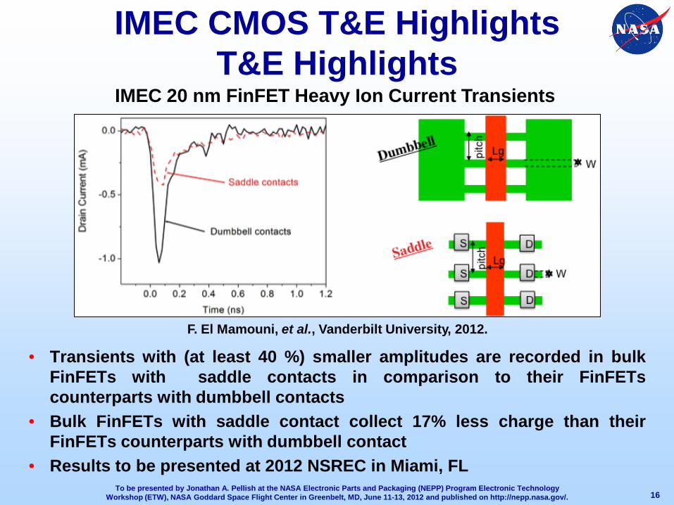
• Transients with (at least 40 %) smaller amplitudes are recorded in bulk FinFETs with saddle contacts in comparison to their FinFETs counterparts with dumbbell contacts
• Bulk FinFETs with saddle contact collect 17% less charge than their FinFETs counterparts with dumbbell contact
• Results to be presented at 2012 NSREC in Miami, FL 16
IMEC 20 nm FinFET Heavy Ion Current Transients
F. El Mamouni, et al., Vanderbilt University, 2012.

To be presented by Jonathan A. Pellish at the NASA Electronic Parts and Packaging (NEPP) Program Electronic Technology Workshop (ETW), NASA Goddard Space Flight Center in Greenbelt, MD, June 11-13, 2012 and published on http://nepp.nasa.gov/.
Low-Energy Proton RHA Highlights
• Given a specific beam line setup, how do you go from degrader thickness to proton energy? – Capture energy and spatial mean & variance
• …in other words: how do you test with low-energy protons?
17
D. F. Heidel et al., TNS, vol. 6, 2008. J. A. Pellish, et al., 2011 SEE Symposium.
45 nm SOI latch

To be presented by Jonathan A. Pellish at the NASA Electronic Parts and Packaging (NEPP) Program Electronic Technology Workshop (ETW), NASA Goddard Space Flight Center in Greenbelt, MD, June 11-13, 2012 and published on http://nepp.nasa.gov/.
Low-Energy Proton RHA Highlights • Realistic setup for an
actual run with degraders – 6.35 μm Ta scattering
foil not shown (~4 m upstream)
– 3x 6.35 μm Al SEEM foils
– Users’ degraders – 127 μm Kapton exit
window – Air gap – Silicon target
18
Silicon Target
Air Gap
Kapton
Aluminum SEEM
Aluminum Degrader
Mylar Degrader
Typical planar stacked target (e.g., SRIM)
≥ 3 cm (Not to scale)
127 μm
≥ 19.05 μm
UC Davis example

To be presented by Jonathan A. Pellish at the NASA Electronic Parts and Packaging (NEPP) Program Electronic Technology Workshop (ETW), NASA Goddard Space Flight Center in Greenbelt, MD, June 11-13, 2012 and published on http://nepp.nasa.gov/.
Low-Energy Proton RHA Highlights
• Measure beam line characteristics – energy, angular dispersion • Simulate experimental conditions when extrapolation is necessary
19
Example SSBD Proton Energy Spectrum SSBD = silicon surface barrier detector
Degraded 50.8 μm aluminum & 3.175 μm Mylar
J. A. Pellish, et al., 2011 IEEE NSREC.

To be presented by Jonathan A. Pellish at the NASA Electronic Parts and Packaging (NEPP) Program Electronic Technology Workshop (ETW), NASA Goddard Space Flight Center in Greenbelt, MD, June 11-13, 2012 and published on http://nepp.nasa.gov/.
FY12 Publications
20
– Summary of work on IBM latches, including RHBD techniques – First published work between NASA/GSFC and Intel on SEE

To be presented by Jonathan A. Pellish at the NASA Electronic Parts and Packaging (NEPP) Program Electronic Technology Workshop (ETW), NASA Goddard Space Flight Center in Greenbelt, MD, June 11-13, 2012 and published on http://nepp.nasa.gov/.
FY12 Publications
21
– Use of scaled CMOS technologies to compare pulsed laser irradiation techniques

To be presented by Jonathan A. Pellish at the NASA Electronic Parts and Packaging (NEPP) Program Electronic Technology Workshop (ETW), NASA Goddard Space Flight Center in Greenbelt, MD, June 11-13, 2012 and published on http://nepp.nasa.gov/. 22
Venus at the Edge Image Credit: JAXA, NASA, Lockheed Martin
http://apod.nasa.gov/apod/ap120609.html
Thank You!
Venus Transit – 2012