Update on JEM FPGA coding. Carsten NödingJohannes Gutenberg-Universität Mainz JEM block diagramm.
9
Update on JEM FPGA coding
-
date post
21-Dec-2015 -
Category
Documents
-
view
215 -
download
2
Transcript of Update on JEM FPGA coding. Carsten NödingJohannes Gutenberg-Universität Mainz JEM block diagramm.
Update on JEM FPGA coding

Carsten Nöding Johannes Gutenberg-Universität Mainz
JEM block diagramm
Processor
(22+11) 5-bit jet elements to neighbours, 80Mb/s
Input FPGA
Input FPGA
Input FPGA
Input FPGA
Input FPGA
Input FPGA
Input FPGA
Input FPGA
Input FPGA
Input FPGA
Input FPGA
33 jet elements from neighbours
44 5-bit jet elements to processor
jet count to merger, 40Mb/s
energy sums to merger, 40Mb/s
VME
control FPGA
TTC
DAQ FPGA
DAQ G-link
ROI G-link
88 LVDS links from PPr 88 de-serialisers
DAQ
LVL-2
CAN
8*10 bit 40Mb/s
8*10 bit
88 pairs@400Mb/s
80Mb/s
jet
energy
configu

Carsten Nöding Johannes Gutenberg-Universität Mainz
Input FPGA
Changes since Birmingham Meeting:
• 256 slices deep playback memory can be written via consecutive single word transfers and read back
• code clean-up

Carsten Nöding Johannes Gutenberg-Universität Mainz
Main Processor

Carsten Nöding Johannes Gutenberg-Universität Mainz
ET,miss, ET
Carsten Nöding Johannes Gutenberg-Universität Mainz
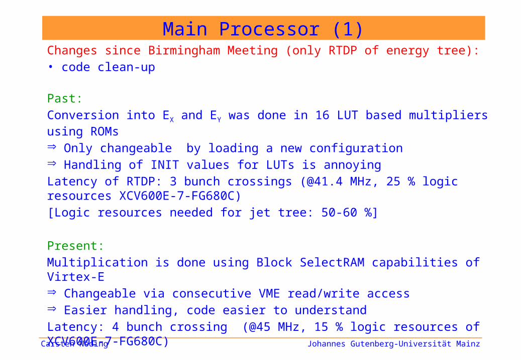
Main Processor (1)Changes since Birmingham Meeting (only RTDP of energy tree):• code clean-up
Past:Conversion into EX and EY was done in 16 LUT based multipliers using ROMs Only changeable by loading a new configuration Handling of INIT values for LUTs is annoyingLatency of RTDP: 3 bunch crossings (@41.4 MHz, 25 % logic resources XCV600E-7-FG680C)[Logic resources needed for jet tree: 50-60 %]
Present:Multiplication is done using Block SelectRAM capabilities of Virtex-E Changeable via consecutive VME read/write access Easier handling, code easier to understandLatency: 4 bunch crossing (@45 MHz, 15 % logic resources of XCV600E-7-FG680C)

Carsten Nöding Johannes Gutenberg-Universität Mainz
Main Processor (2)
Future:
Use Virtex-II device as Main Processor:
Multiplication can done using embedded 18bit by 18bit multipliers
Accuracy is not worsened
Code can be easily adapted (just throw away half of it)
Latency: 2.5 bunch crossings

Carsten Nöding Johannes Gutenberg-Universität Mainz
Reorganisation of JEM Programming Model
Changes since Birmingham Meeting:• Added gaps in register offsets (especially around blocks of related ones, eg. jet thresholds)
things can be changed in the future without having to change the offsets used in any existing software registers which belong together start at some nice boundary
• Module ID words start at address 0 of the module
• Added multiplication registers to store ETsin() and ETcos() results in
BlockRAMs (Virtex-E) same register can be used for storing sin() and cos() in Virtex-II devices
• “separate registers for separate things”
Programming Model has been approved by Murrough Current version can be found in the latest JEM PDR available on the web

Carsten Nöding Johannes Gutenberg-Universität Mainz
Outlook
Main task now:Test of JEM prototype