
University of Victoria - The electronic band structure...
8
The electronic band structure of GaBiAs/GaAs layers: Influence of strain and band anti- crossing Z. Batool, K. Hild, T. J. C. Hosea, X. Lu, T. Tiedje, and S. J. Sweeney Citation: Journal of Applied Physics 111, 113108 (2012); doi: 10.1063/1.4728028 View online: http://dx.doi.org/10.1063/1.4728028 View Table of Contents: http://scitation.aip.org/content/aip/journal/jap/111/11?ver=pdfcov Published by the AIP Publishing Articles you may be interested in Structural and electronic properties of GaAs0.64P0.19Sb0.17 on GaAs Appl. Phys. Lett. 101, 251910 (2012); 10.1063/1.4772550 Temperature and Bi-concentration dependence of the bandgap and spin-orbit splitting in InGaBiAs/InP semiconductors for mid-infrared applications Appl. Phys. Lett. 101, 221108 (2012); 10.1063/1.4768532 Band anticrossing in diluted Al x Ga 1 − x As 1 − y N y ( x 0.37 , y 0.04 ) J. Appl. Phys. 103, 073103 (2008); 10.1063/1.2895002 Characteristics of In Ga P N ∕ Ga As heterostructures investigated by photoreflectance spectroscopy J. Appl. Phys. 100, 093709 (2006); 10.1063/1.2358327 Composition and carrier-concentration dependence of the electronic structure of In y Ga 1 − y As 1 − x N x films with nitrogen mole fraction of less than 0.012 J. Appl. Phys. 98, 093714 (2005); 10.1063/1.2127126 Reuse of AIP Publishing content is subject to the terms at: https://publishing.aip.org/authors/rights-and-permissions. Download to IP: 142.104.83.231 On: Wed, 20 Apr 2016 21:55:27
Transcript of University of Victoria - The electronic band structure...

The electronic band structure of GaBiAs/GaAs layers: Influence of strain and band anti-crossingZ. Batool, K. Hild, T. J. C. Hosea, X. Lu, T. Tiedje, and S. J. Sweeney Citation: Journal of Applied Physics 111, 113108 (2012); doi: 10.1063/1.4728028 View online: http://dx.doi.org/10.1063/1.4728028 View Table of Contents: http://scitation.aip.org/content/aip/journal/jap/111/11?ver=pdfcov Published by the AIP Publishing Articles you may be interested in Structural and electronic properties of GaAs0.64P0.19Sb0.17 on GaAs Appl. Phys. Lett. 101, 251910 (2012); 10.1063/1.4772550 Temperature and Bi-concentration dependence of the bandgap and spin-orbit splitting in InGaBiAs/InPsemiconductors for mid-infrared applications Appl. Phys. Lett. 101, 221108 (2012); 10.1063/1.4768532 Band anticrossing in diluted Al x Ga 1 − x As 1 − y N y ( x 0.37 , y 0.04 ) J. Appl. Phys. 103, 073103 (2008); 10.1063/1.2895002 Characteristics of In Ga P N ∕ Ga As heterostructures investigated by photoreflectance spectroscopy J. Appl. Phys. 100, 093709 (2006); 10.1063/1.2358327 Composition and carrier-concentration dependence of the electronic structure of In y Ga 1 − y As 1 − x N x filmswith nitrogen mole fraction of less than 0.012 J. Appl. Phys. 98, 093714 (2005); 10.1063/1.2127126
Reuse of AIP Publishing content is subject to the terms at: https://publishing.aip.org/authors/rights-and-permissions. Download to IP: 142.104.83.231 On: Wed, 20 Apr 2016
21:55:27

The electronic band structure of GaBiAs/GaAs layers: Influence of strainand band anti-crossing
Z. Batool,1 K. Hild,1 T. J. C. Hosea,1,2,a) X. Lu,3,4 T. Tiedje,5 and S. J. Sweeney1,b)
1Advanced Technology Institute and Department of Physics, University of Surrey, Guildford, Surrey GU2 7XH,United Kingdom2Ibnu Sina Institute for Fundamental Science Studies, Universiti Teknologi Malaysia, Johor Bahru,Johor 81310, Malaysia3Department of Physics and Astronomy, University of British Columbia, Vancouver, V6T 1Z4, Canada4Varian Semiconductor Equipment Associates, Gloucester, Massachusetts 01930, USA5Department of Electrical and Computer Engineering, University of Victoria, Victoria BC, V8W 3P6, Canada
(Received 3 April 2012; accepted 3 May 2012; published online 13 June 2012)
The GaBixAs1�x bismide III-V semiconductor system remains a relatively underexplored alloy
particularly with regards to its detailed electronic band structure. Of particular importance to
understanding the physics of this system is how the bandgap energy Eg and spin-orbit splitting
energy Do vary relative to one another as a function of Bi content, since in this alloy it becomes
possible for Do to exceed Eg for higher Bi fractions, which occurrence would have important
implications for minimising non-radiative Auger recombination losses in such structures. However,
this situation had not so far been realised in this system. Here, we study a set of epitaxial layers of
GaBixAs1�x (2.3%� x� 10.4%), of thickness 30–40 nm, grown compressively strained onto GaAs
(100) substrates. Using room temperature photomodulated reflectance, we observe a reduction in
Eg, together with an increase in Do, with increasing Bi content. In these strained samples, it is
found that the transition energy between the conduction and heavy-hole valence band edges
is equal with that between the heavy-hole and spin-orbit split-off valence band edges at
�9.0 6 0.2% Bi. Furthermore, we observe that the strained valence band heavy-hole/light-hole
splitting increases with Bi fraction at a rate of �15 (61) meV/Bi%, from which we are able to
deduce the shear deformation potential. By application of an iterative strain theory, we decouple
the strain effects from our experimental measurements and deduce Eg and Do of free standing
GaBiAs; we find that Do indeed does come into resonance with Eg at �10.5 6 0.2% Bi. We also
conclude that the conduction/valence band alignment of dilute-Bi GaBiAs on GaAs is most likely
to be type-I. VC 2012 American Institute of Physics. [http://dx.doi.org/10.1063/1.4728028]
I. INTRODUCTION
The bismide alloy GaBixAs1�x has attracted much atten-
tion due to its interesting band structure. The replacement
of a small percentage of arsenic by bismuth in GaAs pro-
duces a giant reduction in the bandgap energy (Eg) of
60–90 meV/%Bi.1–3 This has been described using a valence
band (VB) anti-crossing interaction between the Bi level and
the host GaAs VB (Ref. 3) analogous to conduction band
(CB) anti-crossing now widely reported for dilute nitride
alloys.4 As the result of this anti-crossing, the VBs split into
six valence sub-bands, which may be grouped into the
Eþ(HHþ, LHþ, SOþ) and E_(HH�, LH�, SO�) levels, where
HH and LH refer to heavy and light holes, respectively, and
SO to the spin-orbit split off band.3 As bismuth is the heav-
iest non-radioactive group V element, its alloying to GaAs
enhances the SO splitting energy (Do), and thus, it is also
interesting in the field of spintronics.5 Furthermore, if Do can
be made to be larger than Eg, the valence band Auger process
(conduction, heavy hole)-(split-off hole, heavy hole)
(“CHSH”) (Ref. 6) may be suppressed in the near-infrared
wavelength region. Tailoring both Eg and Do could make
bismides potentially useful, e.g., for improved operating effi-
ciency of 1.3–1.6 lm laser diodes, optical amplifiers, and opti-
cal modulators important for optical fibre communications.7,8
A thorough understanding of the fundamental physical proper-
ties of bismides is therefore crucial. Whilst there are several
reports in the past decade on the structural, optical,1–3,5
thermal,9–11 and transport properties12 of bismides, they
remain a relatively underexplored family of alloys.
Here, we present the results of comprehensive optical
studies of GaBixAs1�x with bismuth concentrations of up to
x¼ 10.4% grown compressively strained on a GaAs sub-
strate. Optical absorption measurements of the fundamental
bandgap energy in GaBixAs1�x with similar high Bi concen-
trations have been reported,13 but the spin-orbit splitting
energy Do has not been measured beyond a concentration of
x¼ 8.4%.3 Here, in addition to a bowing of the band-gap and
spin-orbit splitting energies, we observe a cross over in
energy between the CB-to-HHþ transition and the HHþ-to-
SOþ transition. We also report for the first time the shear
deformation potential (b) for this alloy calculated from the
valence band heavy-hole/light-hole (HHþ-LHþ) splitting. By
application of a novel iterative strain calculation, we are able
to deduce the spin-orbit splitting energy and fundamental
a)E-mail: [email protected])E-mail: [email protected].
0021-8979/2012/111(11)/113108/7/$30.00 VC 2012 American Institute of Physics111, 113108-1
JOURNAL OF APPLIED PHYSICS 111, 113108 (2012)
Reuse of AIP Publishing content is subject to the terms at: https://publishing.aip.org/authors/rights-and-permissions. Download to IP: 142.104.83.231 On: Wed, 20 Apr 2016
21:55:27

bandgap energy in unstrained analogues of our samples and
report the bismuth concentration at which these two energies
become equal, of importance to device applications. Finally,
we comment on the likely conduction/valence band align-
ment configuration of GaBiAs grown on GaAs.
The investigated samples are GaBixAs1�x epilayers,
grown on undoped (100) GaAs by molecular beam epitaxy
with bismuth concentrations of x¼ 2.3%, 4.5%, 8.5%, and
10.4%. The samples are all uncapped with the exception of
the 2.3% sample, which is capped with 300 nm of GaAs. Fur-
ther details about growth can be found in Ref. 14. The thick-
nesses of GaBiAs layers (30–40 nm) are all below the
estimated critical thicknesses1 and so are fully strained
(pseudomorphic) to the GaAs substrate, as confirmed by ear-
lier x-ray diffraction (XRD) studies of Bi concentrations up
to 10%.1,14 As evidence for this, Fig. 1 shows the XRD re-
ciprocal space map of the substrate and GaBiAs film peaks
for the highest concentration studied here of Bi¼ 10.4%.
This demonstrates that the GaBiAs film has the same in-
plane lattice constant as the GaAs substrate, to within the
measurement error of better than 62%.
In order to study the band structure of this material, we
used photomodulated reflectance (PR) spectroscopy, which
is considered to be an excellent technique due to its sensitiv-
ity to critical point transitions in the band structure.15 In this
contactless and non-destructive form of modulated reflec-
tance spectroscopy, the material dielectric function is peri-
odically perturbed by a chopped laser beam. When the laser
is on, it generates electron-hole pairs, which drift apart under
the influence of the in-built electric field and are captured by
traps reducing the magnitude of the field. When the laser is
off, the traps depopulate and the field is restored.16 This
modulates the complex dielectric function of the sample, and
thus the refractive index, which in turn leads to the measured
fractional change in reflectivity DR/R.
II. EXPERIMENT
The interband transition energies between the CB and
HHþ/LHþ VB edges (EgHHþ and Eg
LHþ), and between the
CB and SOþ band edges (EgSOþ), were measured at room
temperature. A 514 nm argon-ion laser line chopped at a fre-
quency of 333 Hz, of power 126 mW, was used to modulate
the same spot on the sample as illuminated by the probe
beam from a tungsten filament lamp and single-grating
monochromator. Phase sensitive detection of the PR signal
was performed with a lock-in amplifier connected to either
InGaAs or Si PIN photodiodes, depending on the wavelength
region being studied. The measured PR spectral line shapes
were least-squares fitted using the sum of two Aspnes third
derivative functional forms (TDFFs) (Ref. 17)
DR=R ¼ Re½CeihðE� Eg þ iCÞ�n�; (1)
where C and h are amplitude and phase variables, E the
energy of the probe beam, Eg the critical point transition
energy, and C a broadening parameter. We investigated the
effect of choosing several of the suggested values for the line
shape exponent factor n (Ref. 17) but found that this had lit-
tle influence on the fitted transition energies. Here, we pres-
ent the results for fits using n¼ 3.
Figure 2(a) shows the resulting room temperature PR
spectra for the four GaBixAs1�x (2.3%� x� 10.4%) samples
in the region of the fundamental bandgap of GaBiAs. The two
low-energy composition-dependent features correspond to the
CB-HHþ and CB-LHþ transitions in GaBixAs1�x, and the
curves show their fits with two TDFFs. The composition-
independent highest-energy transition near 1.43 eV is related
to the GaAs bandgap of the cap/substrate. It may be noted
from Fig. 2(a) that the fit with two TDFFs for the highest bis-
muth concentration of 10.4% is rather poor in the energy
region between the HHþ and LHþ features. This may be an
indication of the predicted emergent effects of stronger LH
interactions with Bi-Bi and Bi cluster states, with increasing
strain and bismuth content.18
Figure 2(b) shows the measured PR features in the region
of the spin-orbit split-off transition, showing the composition-
dependent CB-SOþ transition for the GaBixAs1�x as well as the
corresponding composition-independent SO transition for GaAs.
In Fig. 2(a), we observe a significant composition-
dependent red-shift in the HHþ bandgap energy EgHHþ with
the increasing bismuth concentration. For the 10.4% sample,
a HHþ bandgap wavelength of 1.52 lm has been achieved at
room temperature. In Fig. 2(b), the effect of bismuth concen-
tration of up to 10.4% on the SOþ transition can be seen.
Figure 3 shows the three fitted PR transition energies: EgSOþ,
EgHHþ, and Eg
LHþ. Such a composition dependence of the
interband transitions has been attributed to the band anti-
crossing interaction of the Bi level with the VB of GaAs.3
FIG. 1. XRD reciprocal space map of a GaBixAs1�x film on GaAs substrate
with x¼ 10.4%, for the (115) XRD reflection. The horizontal scale is the in-
plane reciprocal space q vector, and the vertical the out-of-plane q. The
upper cluster of points corresponds to the XRD peak from the GaAs sub-
strate while the lower peak is due to the GaBiAs film, with the intensity indi-
cated by colour (red being the most intense, black the least). Since the film
and substrate have the same in-plane q (and thus the same in-plane lattice
constant), the film is pseudomorphic to the GaAs substrate, to within the
measurement error (<62%).
113108-2 Batool et al. J. Appl. Phys. 111, 113108 (2012)
Reuse of AIP Publishing content is subject to the terms at: https://publishing.aip.org/authors/rights-and-permissions. Download to IP: 142.104.83.231 On: Wed, 20 Apr 2016
21:55:27

The EgHHþ and Eg
LHþ PR features in Fig. 2(a) are due to
the strain-induced VB splitting in this alloy due to the lattice
mismatch to GaAs. Figure 4 shows that the VB splitting
(VBS¼EgLHþ�Eg
HHþ) changes approximately linearly
with bismuth content, at a rate of 15.0 6 1 meV/%Bi, which
is in good agreement with the 15.1 meV/%Bi reported by
Francoeur et al.2 The error bars in Fig. 4 represent the com-
bined uncertainties in the VBS from the associated errors in
the fitted transition energies taken from the least-squares pro-
gram correlation matrix.
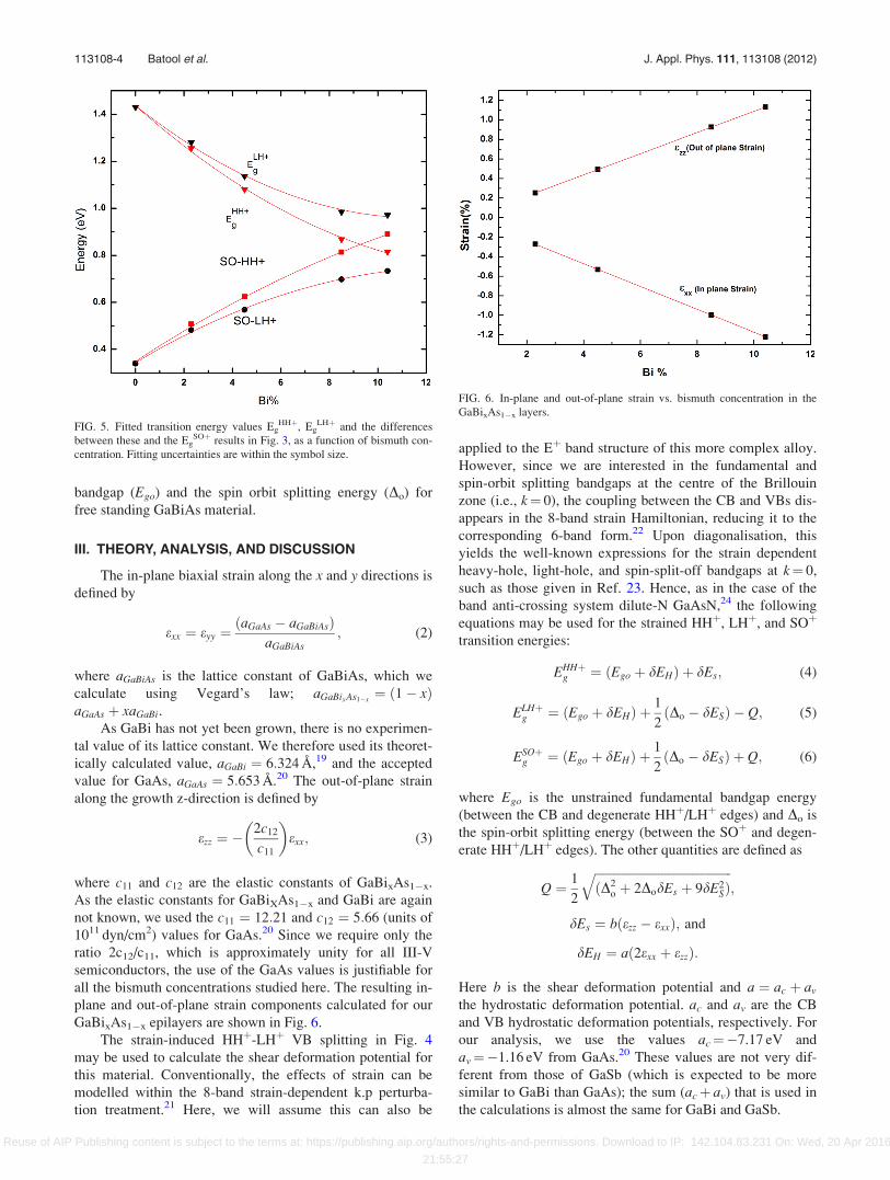
By using the results of Fig. 3, we can plot the splittings
EgSOþ�Eg
HHþ and EgSOþ�Eg
LHþ, which are equivalent to
the transition energy values from the SOþ to HHþ and LHþ
valence band edges, respectively. Figure 5 shows that
EgSOþ�Eg
HHþ, the splitting between the SOþ and the top of
valence band (which is heavy hole in this case) becomes
equal to the observed HHþ transition energy EgHHþ at a bis-
muth concentration of �9.0 6 0.2% in these strained sam-
ples. This result has importance for device applications due
to the possibility of reducing the CHSH Auger losses involv-
ing hole excitation into the spin-orbit band at higher bismuth
concentrations.
By using all our experimental values for these strained
samples, we calculate the deformation potential (b) next and,
by decoupling the effects of strain in our samples, theFIG. 2. (a) Room temperature PR spectra for the four compressively
strained GaBixAs1�x samples studied here, in the region of the fundamental
bandgap. Circles are the experimental data points and solid curves are fits
with a sum of two TDFFs—one each for the HHþ and LHþ features, where
these refer to heavy-(HHþ) and light-hole (LHþ) transitions, respectively.
The feature to the far right is due to the GaAs cap/substrate and does not
vary with bismuth content. The dashed lines are guides to the eye of the ap-
proximate positions of the fitted transition energies. (b) Room temperature
PR spectra for the four compressively strained GaBixAs1�x samples studied
here, in the region of the spin-orbit split off transition. Circles are the experi-
mental data points and solid curves are fits with a sum of two TDFFs—one
for the GaBixAs1�x feature and another for the GaAs feature. The dashed
curves are guides to the eye of the approximate positions of the fitted transi-
tion energies.
FIG. 3. Transition energy values EgHHþ, Eg
LHþ, and EgSOþ obtained by fit-
ting the room temperature experimental PR spectra of Figs. 2(a) and 2(b)
with TDFFs. The curves are only guides to the eye. The fitting uncertainties
are within the symbol size.
FIG. 4. VB splitting (VBS¼EgLHþ�Eg
HHþ) as a function of bismuth con-
centration in our compressively strained GaBixAs1�x samples. The open
circles are the corresponding results of Francoeur et al.2
113108-3 Batool et al. J. Appl. Phys. 111, 113108 (2012)
Reuse of AIP Publishing content is subject to the terms at: https://publishing.aip.org/authors/rights-and-permissions. Download to IP: 142.104.83.231 On: Wed, 20 Apr 2016
21:55:27
bandgap (Ego) and the spin orbit splitting energy (Do) for
free standing GaBiAs material.
III. THEORY, ANALYSIS, AND DISCUSSION
The in-plane biaxial strain along the x and y directions is
defined by
exx ¼ eyy ¼ðaGaAs � aGaBiAsÞ
aGaBiAs; (2)
where aGaBiAs is the lattice constant of GaBiAs, which we
calculate using Vegard’s law; aGaBixAs1�x¼ ð1� xÞ
aGaAs þ xaGaBi.
As GaBi has not yet been grown, there is no experimen-
tal value of its lattice constant. We therefore used its theoret-
ically calculated value, aGaBi ¼ 6:324 A,19 and the accepted
value for GaAs, aGaAs ¼ 5:653 A.20 The out-of-plane strain
along the growth z-direction is defined by
ezz ¼ �2c12
c11
� �exx; (3)
where c11 and c12 are the elastic constants of GaBixAs1�x.
As the elastic constants for GaBiXAs1�x and GaBi are again
not known, we used the c11 ¼ 12:21 and c12 ¼ 5:66 (units of
1011 dyn/cm2) values for GaAs.20 Since we require only the
ratio 2c12/c11, which is approximately unity for all III-V
semiconductors, the use of the GaAs values is justifiable for
all the bismuth concentrations studied here. The resulting in-
plane and out-of-plane strain components calculated for our
GaBixAs1�x epilayers are shown in Fig. 6.
The strain-induced HHþ-LHþ VB splitting in Fig. 4
may be used to calculate the shear deformation potential for
this material. Conventionally, the effects of strain can be
modelled within the 8-band strain-dependent k.p perturba-
tion treatment.21 Here, we will assume this can also be
applied to the Eþ band structure of this more complex alloy.
However, since we are interested in the fundamental and
spin-orbit splitting bandgaps at the centre of the Brillouin
zone (i.e., k¼ 0), the coupling between the CB and VBs dis-
appears in the 8-band strain Hamiltonian, reducing it to the
corresponding 6-band form.22 Upon diagonalisation, this
yields the well-known expressions for the strain dependent
heavy-hole, light-hole, and spin-split-off bandgaps at k¼ 0,
such as those given in Ref. 23. Hence, as in the case of the
band anti-crossing system dilute-N GaAsN,24 the following
equations may be used for the strained HHþ, LHþ, and SOþ
transition energies:
EHHþg ¼ ðEgo þ dEHÞ þ dEs; (4)
ELHþg ¼ ðEgo þ dEHÞ þ
1
2ðDo � dESÞ � Q; (5)
ESOþg ¼ ðEgo þ dEHÞ þ
1
2ðDo � dESÞ þ Q; (6)
where Ego is the unstrained fundamental bandgap energy
(between the CB and degenerate HHþ/LHþ edges) and Do is
the spin-orbit splitting energy (between the SOþ and degen-
erate HHþ/LHþ edges). The other quantities are defined as
Q ¼ 1
2
ffiffiffiffiffiffiffiffiffiffiffiffiffiffiffiffiffiffiffiffiffiffiffiffiffiffiffiffiffiffiffiffiffiffiffiffiffiffiffiffiffiffiffiffiffiðD2
o þ 2DodEs þ 9dE2SÞ
q;
dEs ¼ bðezz � exxÞ; and
dEH ¼ að2exx þ ezzÞ:
Here b is the shear deformation potential and a ¼ ac þ av
the hydrostatic deformation potential. ac and av are the CB
and VB hydrostatic deformation potentials, respectively. For
our analysis, we use the values ac¼�7.17 eV and
av¼�1.16 eV from GaAs.20 These values are not very dif-
ferent from those of GaSb (which is expected to be more
similar to GaBi than GaAs); the sum (acþ av) that is used in
the calculations is almost the same for GaBi and GaSb.
FIG. 5. Fitted transition energy values EgHHþ, Eg
LHþ and the differences
between these and the EgSOþ results in Fig. 3, as a function of bismuth con-
centration. Fitting uncertainties are within the symbol size.
FIG. 6. In-plane and out-of-plane strain vs. bismuth concentration in the
GaBixAs1�x layers.
113108-4 Batool et al. J. Appl. Phys. 111, 113108 (2012)
Reuse of AIP Publishing content is subject to the terms at: https://publishing.aip.org/authors/rights-and-permissions. Download to IP: 142.104.83.231 On: Wed, 20 Apr 2016
21:55:27

If we define the VBS as DLH¼EgLHþ�Eg
HHþ, then
from Eqs. (4) and (5) we have
DLH ¼1
2D0 �
3
2dEs � Q: (7)
If, as suggested by Zhang et al.,24 we were to assume that
D0 � jbðezz � exxÞj in the expression for Q, then using Eq.
(7) we can derive the following approximate expression for
the shear deformation potential:
b � �DLH
2ðezz � exxÞ: (8)
However, this approximation is not necessary here because
we have the additional information needed in Eq. (7) from
our measurements of EgSOþ. From Eq. (7), we obtain
D2o þ 2DodEs þ 9dE2
S ¼ ½ðD0 � 2DLHÞ � 3dEs�2;
from which we get
dEs ¼�DLH
2þ 1
1� DoDLH
� � : (9)
From the definition of
dEs ¼ bðezz � exxÞ;
we then have
b ¼ 1
ðezz � exxÞ� �DLH
2þ 1
1� DoDLH
� � : (10)
Note that Eq. (10) reduces to Eq. (8) if Do� DLH.
In order to use Eq. (10) to obtain b, we require the val-
ues of spin orbit splitting (Do). The theory of Eqs. (4)–(6)
allows us to deduce Do from our experimental measure-
ments, by the following method. Subtracting Eqs. (5) and
(6), we obtain a quantity DSO/LH¼EgSOþ�Eg
LHþ¼ 2Q.
Squaring this and re-arranging, we obtain a quadratic in Do
with the solutions
D0 ¼ �dES6
ffiffiffiffiffiffiffiffiffiffiffiffiffiffiffiffiffiffiffiffiffiffiffiffiffiffiffiffiffiffiffiffiffiffiffiðD2
SO=LH � 8dES2Þ
q: (11)
This, together with Eq. (9), may be solved for Do by the fol-
lowing iteration scheme:
1. Make an initial guess for Do from, say, the bigger of
EgSOþ�Eg
LHþ and EgSOþ�Eg
HHþ (as in Fig. 5).
2. Use this estimate of Do and our experimental value of DLH
to estimate dEs from Eq. (9).
3. Use this dEs and our experimentally measured DSO/LH to
obtain the next estimate of Do from Eq. (11).
4. Repeat steps 2 and 3 until convergence occurs for the Do
value.
Substituting the resulting deduced Do and the values for
DLH, ezz and exx for GaBixAs1�x into Eq. (10) then gives the
shear deformation potential for the different concentrations
of bismuth. We first consider these results for b, as shown in
Fig. 7, and discuss the Do results later.
The error bars in Fig. 7 come from considering mainly
the errors in the VBS in Eq. (10), as shown in Fig. 4. Thus,
the calculated error bar for b is largest in the 2.3% sample,
due to the close proximity of the HHþ and LHþ features in
the PR spectra, and the consequently proportionally higher
fitting errors in the VBS. Figure 7 shows that the deformation
potential for compressively strained GaBiAs layers is com-
position dependent, as has been found for the dilute-N
GaAsN alloys.24 Due to the big difference in the size of the
bismuth atom, as compared to the arsenic atom it replaces, a
shear strain field is induced in its vicinity, which is responsi-
ble for the perturbations in the VBS and deformation poten-
tial.25 In the case of N in GaAs, Zhang et al.24 argue that as
the nitrogen content increases, these local strain fields inter-
act and lead to an overall additional strain, which will in turn
lead to an increase in the VBS. The GaAsN b has an even
more complex composition dependence on N content24 than
in our case of GaBiAs, which appears approximately linearly
dependent on bismuth content up to 10.4% (see Fig. 7). The
reason for this dependence is not understood for this new
alloy at present.
Once Do and b have been deduced by the above meth-
ods, we can then use Eq. (4), say, to deduce the unstrained
bandgap energy for free-standing GaBiAs, Ego ¼ EHHþg �
ðdEH þ dEsÞ; from our measurement of EgHHþ (Fig. 3), the
known values of a and b (from Fig. 7), and the calculated
strains exx and ezz (from Fig. 6).
The resulting deduced spin-orbit splitting energy and
unstrained bandgap energy are shown in Fig. 8 (filled trian-
gles). We estimate from a small extrapolation of the curves
in Fig. 8 that the energy cross-over Do¼Ego would occur at
bismuth concentrations of 10.5 6 0.2% for such free-
standing GaBiAs.
FIG. 7. Deduced shear deformation potential of coherently compressively
strained GaBixAs1�x on a GaAs substrate as a function of bismuth concen-
tration. The linear fit gives a gradient of 163 meV/%Bi.
113108-5 Batool et al. J. Appl. Phys. 111, 113108 (2012)
Reuse of AIP Publishing content is subject to the terms at: https://publishing.aip.org/authors/rights-and-permissions. Download to IP: 142.104.83.231 On: Wed, 20 Apr 2016
21:55:27
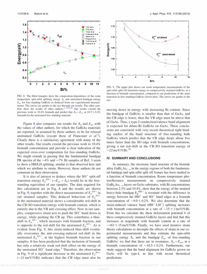
Figure 8 also compares our results for Do and Ego with
the values of other authors, for which the GaBiAs materials
are reported, or assumed by those authors, to be for relaxed
unstrained GaBiAs (except those of Francouer et al.2).
Clearly there is a satisfactory agreement with many of the
other results. Our results extend the previous work to 10.4%
bismuth concentration and provide a clear indication of the
expected cross-over composition for free-standing GaBiAs.
We might remark in passing that the fundamental bandgap
PR spectra of the �4% and �7% Bi samples of Ref. 3 seem
to show a HH/LH splitting, similar to that observed here and
which we attribute to strain. However, those authors do not
comment on their observation.
It is also of interest to deduce where the SOþ split-off
transition energy EgSOþ (¼EgoþDo) would lie in the free-
standing equivalent of our samples. The data required for
this calculation are in Fig. 8 and the results are shown
in Fig. 9, together with the direct measurements of EgSOþ in
our strained samples. This deduced behaviour of EgSOþ
in the unstrained material shows a considerable red-shift in
the CB-SO transition energy with bismuth content, which is
entirely due to the VB anti-crossing effect. Now in our sam-
ples, compressive strain acts to push the SOþ band down in
energy, while pushing the CB up. This contributes a blue-
shift to EgSOþ, which increases with bismuth fraction, and
is opposite to the red-shift for the unstrained EgSOþ. As is
evident from Fig. 9, this strain-induced blue-shift eventu-
ally overcomes the anti-crossing-induced red-shift in the
unstrained EgSOþ, at the highest bismuth fraction in our
samples. It has been predicted that the inclusion of bismuth
has only a relatively weak red-shift effect on the energy of
the unstrained SOþ band edge.3 Therefore, the observation
in Fig. 9 of a significant decrease in the unstrained EgSOþ
(�21 meV/%Bi) indicates that the CB edge must also be
moving down in energy with increasing Bi content. Since
the bandgap of GaBiAs is smaller than that of GaAs, and
the CB edge is lower, then the VB edge must be above that
of GaAs. Thus, a type-I conduction/valence band alignment
is expected for dilute-Bi GaBiAs on GaAs. These conclu-
sions are consistent with very recent theoretical tight bind-
ing studies of the band structure of free-standing bulk
GaBiAs which predict that the CB edge drops about five
times faster than the SO edge with bismuth concentration,
giving a net red-shift in the CB-SO transition energy of
�22 meV/%Bi.18
IV. SUMMARY AND CONCLUSIONS
In summary, the electronic band structure of the bismide
alloy GaBixAs1�x in the energy regions of both the fundamen-
tal bandgap and spin orbit split off feature has been studied as
a function of bismuth concentration. Room temperature pho-
toreflectance measurements on compressively strained
GaBixAs1�x layers on GaAs substrates, with Bi concentrations
between 2.3% and 10.4%, show that the energy of the strained
heavy-hole bandgap EgHHþ is resonant with the difference in
energy between the HHþ and SOþ band edges at a bismuth
concentration of �9.0 6 0.2%. We also determine that the
strain-induced valence band (HHþ-LHþ) splitting increases
with bismuth concentration at a rate of �15 6 1 meV/%Bi.
From this we calculate the shear deformation potential b of
these compressively strained GaBiAs layers and find that this
increases in magnitude with bismuth content at a rate of
�163 6 15 meV/%Bi. Finally, we have used iterative strain
theory calculations to decouple the effects of strain in our ex-
perimental measurements and thus estimate the spin-orbit
splitting energy Do and the bandgap Ego of free-standing
GaBiAs: we find that these are in resonance, Do¼Ego, at a
bismuth concentration of �10.5 6 0.2%. Furthermore, our
study suggests that the band alignment for GaBiAs grown on
GaAs will be type-I, in line with recent theoretical
predictions.
FIG. 8. The filled triangles show the composition-dependence of the room
temperature spin-orbit splitting energy Do and unstrained bandgap energy
Ego for free-standing GaBiAs as deduced from our experimental measure-
ments. The curves are guides to the eye through our results. The other sym-
bols show the results of other authors.1–3,5,9,26 Our results extend the
previous work to 10.4% bismuth and predict that Do¼Ego at 10.5 6 0.2%
bismuth for the unstrained free-standing material.
FIG. 9. The upper plot shows our room temperature measurements of the
spin-orbit split-off transition energy in compressively strained GaBiAs, as a
function of bismuth concentration, compared to our predictions of the same
transition in free-standing GaBiAs (lower plot). The curves are guides to the
eye.
113108-6 Batool et al. J. Appl. Phys. 111, 113108 (2012)
Reuse of AIP Publishing content is subject to the terms at: https://publishing.aip.org/authors/rights-and-permissions. Download to IP: 142.104.83.231 On: Wed, 20 Apr 2016
21:55:27

ACKNOWLEDGMENTS
Z.B. gratefully acknowledges the support of the “The
Islamia University of Bahawalpur, Pakistan” for providing a
studentship under the Faculty Development Program (FDP)
and also further partial support from the “Surrey Kwan Trust
Fund.” This work was also partially funded by the EPSRC
under EP/G064725/1. T.J.C.H. thanks the “Malaysian Uni-
versity Grant Program (GUP) Tier 1,” Universiti Teknologi
Malaysia and M.O.H.E. (Q.J130000.7126.01H55). We are
grateful to Vahid Bahrami Yekta and Mostafa Masnadi of
the University of Victoria, Canada, for providing the XRD
measurements of Fig. 1.
1S. Tixier, M. Adamcyk, T. Tiedje, S. Franceour, A. Mascarenhas, P. Wei,
and F. Schiettekatte, Appl. Phys. Lett. 82, 2245 (2003).2S. Francoeur, M. J. Seong, A. Mascarenhas, S. Tixier, M. Adamcyk, and
T. Tiedje, Appl. Phys. Lett. 82, 3874 (2003).3K. Alberi, O. D. Dubon, W. Walukiewicz, K. M. Yu, K. Bertulis, and A.
Krotkus, Appl. Phys. Lett. 91, 051909 (2007).4Y. Zhang, A. Mascarenhas, and L. W. Wang, Phys. Rev. B 71, 155201
(2005).5B. Fluegel, S. Francoeur, A. Mascarenhas, S. Tixier, E. C. Young, and T.
Tiedje, Phys. Rev. Lett. 97, 067205 (2006).6J. P. Loehr and J. Singh, IEEE J. Quantum Electron. 29, 2583 (1993).7S. J. Sweeney, Photonics West 2010, Paper [7616-11] (2010).8S. J. Sweeney, WO patent 2010/149978 (2010).9J. Yoshida, T. Kita, O. Wada, and K. Oe, Jpn. J. Appl. Phys. 42, 371 (2003).
10K. Oe, Jpn. J. Appl.Phys. 41, 2801 (2002).11G. Pettinari, A. Polimeni, M. Capizzi, J. H. Blokland, P. C. M. Christianen,
J. C. Maan, E. C. Young, and T. Tiedje, Appl. Phys. Lett. 92, 262105
(2008).12D. G. Cooke, F. A. Hegmann, E. C. Young, and T. Tiedje, Appl. Phys.Lett.
89, 122103 (2006).13V. Pacebutas, K. Bertulis, G. Aleksejenko, and A. Krotkus, J. Mater. Sci:
Mater. Electron. 20, S363 (2008).14X. Lu, D. A. Beaton, R. B. Lewis, T. Tiedje, and Y. Zhang, Appl. Phys.
Lett. 95, 041903 (2009); X. Lu, D. A. Beaton, R. B. Lewis, T. Tiedje, and
M. B. Whitwick, ibid. 92, 192110 (2008).15F. H. Pollak, Handbook on Semiconductors, edited by T. S. Moss (Elsev-
ier, Amsterdam, 1994), Vol. 2, p. 527.16H. Shen, Z. Hang, S. H. Pan, F. H. Pollak, and J. M. Woodall, Appl. Phys.
Lett. 52, 2058 (1988).17D. E. Aspnes, Surf. Sci. 37, 418 (1973).18M. Usman, C. A. Broderick, A. Lindsay, and E. P. O’Reilly, Phys. Rev. B
84, 245202 (2011).19A. Janotti, S.-H. Wei, and S. B. Zhang, Phys. Rev. B. 65, 115203 (2003).20I. Vurgaftman, J. R. Meyer, and L. R. Ram-Mohan, J. Appl.Phys. 89, 5825
(2001).21T. B. Bahder, Phys. Rev. B 41, 11992 (1990).22C. Pryor, Phys. Rev. B 57, 7190 (1998).23F. H. Pollak, Semiconductors and Semimetals, edited by T. P. Pearsall
(Academic, New York, 1990), Vol. 32, p. 17.24Y. Zhang, A. Mascarenhas, H. P. Xin, and C. W. Tu, Phys. Rev. B 61,
4433 (2000).25T. N. Morgan, in Proceedings of the 10th International Conference on the
Physics of Semiconductors, August 17–21, 1970, p. 266.26W. Huang, K. Oe, G. Feng, and M. Yoshimoto, J. Appl. Phys. 98, 053505
(2005).
113108-7 Batool et al. J. Appl. Phys. 111, 113108 (2012)
Reuse of AIP Publishing content is subject to the terms at: https://publishing.aip.org/authors/rights-and-permissions. Download to IP: 142.104.83.231 On: Wed, 20 Apr 2016
21:55:27