University of Southampton Research Repository ePrints … · Nowadays, mod-ern optical...
225
University of Southampton Research Repository ePrints Soton Copyright © and Moral Rights for this thesis are retained by the author and/or other copyright owners. A copy can be downloaded for personal non-commercial research or study, without prior permission or charge. This thesis cannot be reproduced or quoted extensively from without first obtaining permission in writing from the copyright holder/s. The content must not be changed in any way or sold commercially in any format or medium without the formal permission of the copyright holders. When referring to this work, full bibliographic details including the author, title, awarding institution and date of the thesis must be given e.g. AUTHOR (year of submission) "Full thesis title", University of Southampton, name of the University School or Department, PhD Thesis, pagination http://eprints.soton.ac.uk
Transcript of University of Southampton Research Repository ePrints … · Nowadays, mod-ern optical...

University of Southampton Research Repository
ePrints Soton
Copyright © and Moral Rights for this thesis are retained by the author and/or other copyright owners. A copy can be downloaded for personal non-commercial research or study, without prior permission or charge. This thesis cannot be reproduced or quoted extensively from without first obtaining permission in writing from the copyright holder/s. The content must not be changed in any way or sold commercially in any format or medium without the formal permission of the copyright holders.
When referring to this work, full bibliographic details including the author, title, awarding institution and date of the thesis must be given e.g.
AUTHOR (year of submission) "Full thesis title", University of Southampton, name of the University School or Department, PhD Thesis, pagination
http://eprints.soton.ac.uk

UNIVERSITY OF SOUTHAMPTON
DEPOSITION OF ELECTRONIC AND PLASMONIC
MATERIALS INSIDE MICROSTRUCTURED OPTICAL
FIBRES
by
Adrian Amezcua Correa
A thesis submitted in partial fulfillment for the
degree of Doctor of Philosophy
in the
Faculty of Engineering, Science and Mathematics
Optoelectronics Research Centre
November 2007
UNIVERSITY OF SOUTHAMPTON
ABSTRACT
FACULTY OF ENGINEERING, SCIENCE AND MATHEMATICS
OPTOELECTRONICS RESEARCH CENTRE
Doctor of Philosophy
DEPOSITION OF ELECTRONIC AND PLASMONIC MATERIALS
INSIDE MICROSTRUCTURED OPTICAL FIBRES
by Adrian Amezcua Correa
Optical fibres are the transport medium of today’s digital information. Nowadays, mod-
ern optical telecommunication systems make use of semiconductor optoelectronic devices
to generate, control and detect light. The union of the two technologies, namely fibre
photonics and semiconductor electronics is expected to have a major impact on next gen-
eration of optoelectronic devices, exploiting both the guiding capabilities of optical fibres
and the signal processing properties of semiconductors devices. Only recently, with the
advent of microstructured optical fibres and templating material processing methods, it
has been possible to create optical fibres with solid-state material inclusions.
This thesis describes the development of various high-pressure chemical deposition meth-
ods for the formation of extreme aspect ratio tubes and wires of semiconductors, metals
and other functional materials within the capillary holes of microstructured optical fi-
bres. Fabrication of composite structures in this way provides optical fibres with a
number of new electronic, photonic and plasmonic degrees of freedom.
An in-depth study into the material, optical and electrical properties of these new com-
posite fibres is presented. TEM, SEM and micro-Raman analysis was used to determine
the structural characteristics of silicon and germanium-modified microstructured optical
fibres. These studies demonstrate that single crystal, poly-crystalline and amorphous
semiconductors can be conformally deposited within the capillary voids of microstruc-
tured optical fibres. As a step towards fibre-integrated optoelectronic devices, it is
demonstrated that in-fibre silicon and germanium wires and tubes can function as field
effect transistors and light waveguides.
An experimental investigation on the optical transmission properties of microstructured
optical fibres impregnated with silver nanoparticles is also presented. These fibres are
shown to be an excellent way of coupling optical guided modes into surface plasmons. As
a result, they represent a promising platform technology for fully integrated photonic-
plasmonic devices. These fibres have demonstrated the enhancement of Raman signals
from molecules adsorbed onto the inner metal surfaces and thus ideally suited for Surface
Enhance Raman Scattering molecular detection.

Declaration of Authorship
I, Adrian Amezcua Correa, declare that this thesis entitled:
DEPOSITION OF ELECTRONIC AND PLASMONIC MATERIALS INSIDE
MICROSTRUCTURED OPTICAL FIBRES
and the work presented in it are my own. I confirm that:
• This work was done wholly or mainly while in candidature for a research
degree at this University
• Where any part of this thesis has previously been submitted for a degree or
any other qualification at this University or any other institution, this has
been clearly stated
• Where I have consulted the published work of others, this is always clearly
attributed
• Where I have quoted from the work of others, the source is always given.
With the exception of such quotations, this thesis is entirely my own work
• I have acknowledged all main sources of help
• Where the thesis is based on work done by myself jointly with others, I have
made clear exactly what was done by others and what I have contributed
myself
Adrian Amezcua Correa
November 2007
ii

Contents
1 Introduction 1
1.1 Past and Current Work . . . . . . . . . . . . . . . . . . . . . . . . . 4
1.2 Thesis Structure . . . . . . . . . . . . . . . . . . . . . . . . . . . . . 8
2 Microstructured Optical Fibres 11
2.1 History of MOFs . . . . . . . . . . . . . . . . . . . . . . . . . . . . 11
2.2 Fabrication of MOFs . . . . . . . . . . . . . . . . . . . . . . . . . . 13
2.3 Fundamentals of Photonic Crystals . . . . . . . . . . . . . . . . . . 15
2.4 Step-Index Optical Fibres . . . . . . . . . . . . . . . . . . . . . . . 19
2.5 Index-Guiding MOFs . . . . . . . . . . . . . . . . . . . . . . . . . . 20
2.6 Optical Properties of MOFs . . . . . . . . . . . . . . . . . . . . . . 21
2.6.1 Endlessly Single Mode Operation . . . . . . . . . . . . . . . 21
2.6.2 Group Velocity Dispersion . . . . . . . . . . . . . . . . . . . 22
2.6.3 Nonlinear Optics . . . . . . . . . . . . . . . . . . . . . . . . 23
2.7 Modelling Microstructured Optical Fibres . . . . . . . . . . . . . . 25
2.7.1 Full-vector Plane-wave Expansion Method (FVPWE) . . . . 26
2.7.2 Orthogonal Basis Functions Techniques . . . . . . . . . . . . 26
2.7.3 Beam Propagation Method . . . . . . . . . . . . . . . . . . . 27
2.8 Semiconductor Photonic Bandgap Fibres . . . . . . . . . . . . . . . 27
3 Materials Deposition inside Microstructured Optical Fibres 30
3.1 Micro/Nanomaterials Synthesis . . . . . . . . . . . . . . . . . . . . 31
3.2 Vapour Phase Deposition . . . . . . . . . . . . . . . . . . . . . . . . 33
3.2.1 Physical Vapour Deposition . . . . . . . . . . . . . . . . . . 33
3.2.1.1 Thermal Vapour Deposition (TVD) . . . . . . . . . 34
3.2.1.2 Sputtering . . . . . . . . . . . . . . . . . . . . . . . 34
3.2.2 Chemical Vapour Deposition . . . . . . . . . . . . . . . . . . 35
3.3 Liquid Phase Deposition . . . . . . . . . . . . . . . . . . . . . . . . 38
3.3.1 Electrochemical Deposition . . . . . . . . . . . . . . . . . . . 39
3.3.2 Electroless Deposition . . . . . . . . . . . . . . . . . . . . . 39
3.4 Supercritical Fluid Deposition . . . . . . . . . . . . . . . . . . . . . 41
3.5 High-Pressure Chemical Vapour Deposition inside MOFs . . . . . . 43
3.5.1 High-Pressure CVD of Silicon inside MOFs . . . . . . . . . . 46
3.5.2 High-Pressure CVD of Germanium inside MOFs . . . . . . . 49
3.6 Vapor Liquid Solid Growth of Single-Crystal Silicon inside MOFs . 52
iii
Contents iv
3.7 SCFD of Silver Nanoparticles inside MOFs . . . . . . . . . . . . . . 54
3.8 SCFD of Polymers inside MOFs . . . . . . . . . . . . . . . . . . . . 56
4 Semiconductor Modified Optical Fibres 59
4.1 Structural Characterisation of Semiconductor MOFs . . . . . . . . . 59
4.1.1 Transmission Electron Microscopy (TEM) . . . . . . . . . . 61
4.1.1.1 Diffraction Patterns of Silicon MOFs . . . . . . . . 64
4.1.1.2 Diffraction Patterns of Germanium MOFs . . . . . 65
4.1.2 Raman Spectroscopy . . . . . . . . . . . . . . . . . . . . . . 69
4.1.2.1 Raman Spectroscopy of Silicon modified MOFs . . 70
4.1.2.2 Raman Spectroscopy of Germanium . . . . . . . . 80
4.2 Electrical Characterisation . . . . . . . . . . . . . . . . . . . . . . . 81
4.2.1 Electrical Properties of Germanium Fibres . . . . . . . . . . 83
4.2.2 Electrical Properties of Silicon Fibres . . . . . . . . . . . . . 85
4.3 Optical Characterisation of Silicon MOFs . . . . . . . . . . . . . . . 88
4.3.1 Silicon Optical Fibres . . . . . . . . . . . . . . . . . . . . . . 89
4.3.2 In-Fibre Silicon Modulator . . . . . . . . . . . . . . . . . . . 94
5 Optical Properties of Metal Nanoparticles 96
5.1 Introduction . . . . . . . . . . . . . . . . . . . . . . . . . . . . . . . 96
5.2 Classical Optics of Metals . . . . . . . . . . . . . . . . . . . . . . . 98
5.3 Optical Response of Bound Electrons (Lorentz Model) . . . . . . . 100
5.4 Optical Response of Free Electrons (Drude Model) . . . . . . . . . . 100
5.5 Real Metals . . . . . . . . . . . . . . . . . . . . . . . . . . . . . . . 102
5.6 Surface Plasmons Polaritons . . . . . . . . . . . . . . . . . . . . . . 104
5.7 Localized Surface Plasmons . . . . . . . . . . . . . . . . . . . . . . 107
5.8 Plasmonic Devices and Applications . . . . . . . . . . . . . . . . . . 109
5.8.1 Sensors and Biosensors . . . . . . . . . . . . . . . . . . . . . 109
5.8.2 Extraordinary Optical Transmission . . . . . . . . . . . . . . 111
5.8.3 Photonic Integration . . . . . . . . . . . . . . . . . . . . . . 112
6 Surface Enhanced Raman Scattering 113
6.1 Raman Effect . . . . . . . . . . . . . . . . . . . . . . . . . . . . . . 114
6.1.1 Theory of the Raman Effect . . . . . . . . . . . . . . . . . . 116
6.2 Resonance Raman Scattering . . . . . . . . . . . . . . . . . . . . . 118
6.3 Surface Enhanced Raman Scattering . . . . . . . . . . . . . . . . . 118
6.3.1 Enhancement Theories . . . . . . . . . . . . . . . . . . . . . 119
6.3.1.1 Electromagnetic Mechanism . . . . . . . . . . . . . 120
6.3.1.2 Chemical Enhancement . . . . . . . . . . . . . . . 123
7 Metal Modified Optical Fibres 126
7.1 Introduction . . . . . . . . . . . . . . . . . . . . . . . . . . . . . . . 126
7.2 Transmission Properties of MOFs with Metal Inclusions . . . . . . . 128
7.3 SERS Characterisation . . . . . . . . . . . . . . . . . . . . . . . . . 132
7.3.1 Fibres with Different Geometries . . . . . . . . . . . . . . . 138

Contents v
7.3.2 Remote SERS Sensing . . . . . . . . . . . . . . . . . . . . . 140
7.4 Efficient Electrical Characterisation of the SERS Substrates . . . . 141
8 Semiconductor Quantum Dots 143
8.1 Introduction . . . . . . . . . . . . . . . . . . . . . . . . . . . . . . . 143
8.2 Synthesis of PbSe Quantum Dots . . . . . . . . . . . . . . . . . . . 145
8.3 Optical Characterisation of Semiconductor Nanocrystals . . . . . . 149
9 Conclusions 156
9.1 Summary of Results . . . . . . . . . . . . . . . . . . . . . . . . . . 156
9.2 Future Devices and Work . . . . . . . . . . . . . . . . . . . . . . . . 159
A Quantum Confinement Effects 162
A.1 Crystal Structure . . . . . . . . . . . . . . . . . . . . . . . . . . . . 162
A.2 Electron Diffraction by Crystals . . . . . . . . . . . . . . . . . . . . 164
A.3 Quantum Confinement Effects . . . . . . . . . . . . . . . . . . . . . 165
B List of Publications 169
Bibliography 173

List of Figures
1.1 SEM cross sectional micrographs of different microstructured optical fi-bres fabricated at the ORC. The central fibres are among the most ad-vanced kind of MOFs as they can guide light in their hollow core byphotonic band gap mechanisms. . . . . . . . . . . . . . . . . . . . . . . . . 3
1.2 The deposition of semiconductors and metals within the capillary holesof microstructured optical allow for the fusion of two powerful technolo-gies: semiconductor and microstructured optical fibres technologies forthe creation of a new class of metamaterials. This gives room for the de-velopment of interesting in-fibre electronic, optoelectronic and plasmonicdevices. . . . . . . . . . . . . . . . . . . . . . . . . . . . . . . . . . . . . . 4
1.3 This butterfly is an example of how the micro-scale architecture of adielectric medium gives rise to fantastic optical effects. Its wings prohibitthe transmission of blue light which produces a striking blue coloration,adapted from reference [27]. Right: first 3D human-made photonic crystaloperating at infrared wavelengths, from reference [28]. . . . . . . . . . . . 5
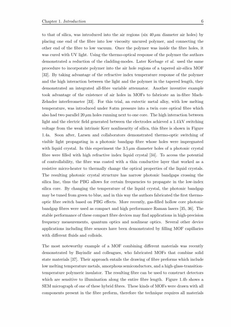
1.4 (a) Example of a MOF filled with Bi and Sn metal eutectic. The meltingtemperature of the eutectic is 137 C and the pressure used to intro-duce the liquid metal into the 20µm fibre holes was 8 atm. The result-ing fibre was used as a Mach-Zehnder amplitude modulator, from ref-erence [33]. (b) Cross-sectional SEM micrograph of a hollow-core metal-semiconductor-insulator fibre. The upper inset shows the omnidirectionalmirror which is formed by an array of quarter-wave As2Se3 and PEI lay-ers. Also a metallic, Sn, filament which is used as the conductive mediumof the in-fibre detector is shown in the inset. The lower inset is a pictureof 1 m long, 1 mm thick hybrid fibre, taken from reference [37]. . . . . . . 7
1.5 (a) Empty air silica MOF template, the scale bar in the inset is 2 µm.Despite the fragile appearance of the thin ( < 100 nm) capillary walls, thisfigure illustrates how robust these fibres are. MOF are able to support thehigh precursor pressure required for the deposition process. (b) Conformaldeposition of polycrystalline silicon within the MOF holes using a highpressure material deposition technique, the scale bar is 1 µm. . . . . . . . 8
2.1 (a) First demonstration of a MOF, taken from reference [45]. (b) FirstMOF with a silica core surrounded by a periodic array of air holes insilica, from reference [9]. . . . . . . . . . . . . . . . . . . . . . . . . . . . 13
2.2 Top, examples of (a) solid core and (b) air core MOFs preforms fabricatedby stacking silica capillaries and rods. Bottom, SEM micrographs of theMOFs which have the same geometry as their preform. . . . . . . . . . . . 14
2.3 Schematic diagram for a drawing tower. . . . . . . . . . . . . . . . . . . . 15
vi
List of Figures vii
2.4 SEM micrographs of MOFs with periodic arrangement of nanoscale holes(a) the diameter of the holes is ∼450 nm. (b) The diameter of the holesis ∼ 250 nm. . . . . . . . . . . . . . . . . . . . . . . . . . . . . . . . . . . . 16
2.5 Schematic illustration of the cross-section and refractive-index profile ofa SMF. The bottom image shows guidance by TIR. . . . . . . . . . . . . . 19
2.6 Top: Transverse cross-section of a solid core MOFs. The white and greyregions are air and silica respectively. The photonic crystal cladding isan ideal hexagonal lattice with parameters: pitch Λ and hole diameterd. The refractive index profile of fibre the is shown in the middle. Thebottom images illustrate the modified TIR guidance mechanisms. . . . . . 21
2.7 Supercontinuum laser generation using a high nonlinear MOF. Nanosec-ond infrared pulses are coupled into the fibre core where visible light isgenerated due to nonlinear processes. The photograph shows the nonlin-ear fibre and a prism used as a diffraction medium. This laser has beenused for plasmon experiments in Chapter 7. . . . . . . . . . . . . . . . . . 24
2.8 Transverse index profile of a MOF with triangular lattice. A thin siliconlayer is deposited on the hole walls. The silicon is represented by redcolour, silica by gray and the black region is air. A missing hole in thecentre forms its silica core. The pitch Λ, silicon thickness t and hole radiusa can be modified for the simulations. . . . . . . . . . . . . . . . . . . . . 29
2.9 Bandgap map for the 16 lowest-frequency modes of a the fibre show inFigure 2.8. The parameters used in the simulation were Λ = 2µm, a =1µm and t = 150nm. . . . . . . . . . . . . . . . . . . . . . . . . . . . . . . 29
3.1 Cartoon of top-down and bottom-up nanofabrication techniques. Fromreference [100]. . . . . . . . . . . . . . . . . . . . . . . . . . . . . . . . . . 31
3.2 The green colour of Parides sesostris is created by an “inverse opal”photonic crystal which is made by templating and self-assembly methods[27]. Nanostructures in nature do not only have optical functionalities butalso mechanical purposes, as has the glasshouse of marine diatoms. (b)SEM micrograph of the silica wall of the marine benthic diatom Amphora
coffea-formis, the scale bar is 5 µm. This ordered silica nanostructure ismade by the deposition of silica in organic matrices [101]. . . . . . . . . . 32
3.3 Illustration of a typical TVD deposition chamber. Only materials witha much higher vapor pressure than the heating element can be depositedwithout contamination of the film. TVD requires good vacuum duringevaporation, and pressures lower than 10−6 Pa are normally used. . . . . . 35
3.4 Schematic diagram of a simple sputtering deposition chamber. . . . . . . . 36
3.5 A schematic diagram of a hot wall open flow CVD system. All substratescan be covered homogeneously because of the low surface reaction rateof the growth process. The total pressure in the chamber is usually lessthan 60 kPa. . . . . . . . . . . . . . . . . . . . . . . . . . . . . . . . . . . . 36
3.6 Synthesis of gold nanowires in porous alumina template by electrochem-ical deposition. Left: TEM image of a microtomed section of aluminamembrane. Right: TEM of Au nanotubes that are 70 nm in diameterwithin the pores of a membrane, from reference [131]. . . . . . . . . . . . 40
List of Figures viii
3.7 Synthesis of gold micro-tubes in a 5µm silica capillary by electroless de-position (end and side views). Silica capillaries (A) are modified witha monolayer of bifunctional silane for gold adhesion (B), deposition ofa monolayer of colloidal gold (C). Deposition of bulk gold from solutionincreases the size of the gold layer, eventually forming a uniform layer(D). As deposition progresses, the gold thickness approaches the radiusof the capillary (E), microscope images of the resulting gold tubes (F GH). Taken from reference [38] . . . . . . . . . . . . . . . . . . . . . . . . . 40
3.8 Pressure-temperature phase diagram for a pure substance. The blue cir-cles illustrate the variation in the substance density. The triple point(T), critical point (C) and the SCF state are all displayed (adapted fromreference [140]). . . . . . . . . . . . . . . . . . . . . . . . . . . . . . . . . . 41
3.9 (a) SEM micrograph of SCF deposition of copper films into features asnarrow as 45 nm on a silicon wafer, from reference [42]. (b) SEM micro-graph of self-supporting gold arrays deposited by SCFD onto mesoporoussilicon. The micrograph was obtained after removing the substrate, fromreference [144]. . . . . . . . . . . . . . . . . . . . . . . . . . . . . . . . . . 42
3.10 High-pressure chemical deposition process for fabricating semiconductorstructures within micro/nanoscale pores of MOFs. The process occursover lengths of tens of centimeters inside capillary holes as small as 100nm. . . . . . . . . . . . . . . . . . . . . . . . . . . . . . . . . . . . . . . . 45
3.11 HP-CVD process for deposition of silicon wires inside micro/nanoscalecapillaries of MOFs using silane precursor. The high-pressure flow allowsfor transport of reactants deep inside the extreme aspect holes and enablesuniform, dense and conformal annular deposition of silicon. . . . . . . . . 47
3.12 SEM micrographs of silicon annular deposition by HP-CVD method withinmicro/nano sized MOFs. a) 6µm diameter silica capillary filled with sil-icon. The internal hole diameter after the deposition is only 1µm. Theinset shows the whole structure for clarity, scale bars are 2µm and 20µmrespectively. b) silicon within a 2µm silica capillary, scale bar 1µm. c)Array of filled nanoscale holes, scale bar is 3µm (see Figure 2.4 for fibretemplate). d) Twin hole MOF with 30µm diameter lateral holes, scalebar is 100µm . . . . . . . . . . . . . . . . . . . . . . . . . . . . . . . . . . 47
3.13 SEM micrographs of silicon annular deposition by the HP-CVD methodwithin a honeycomb MOF. a) MOF template before silicon deposition,scale bars is 2µm. b) silicon deposition inside a honeycomb MOF, scalebar is 2µm c) Another example of silicon deposition within the holes ofa honeycomb fibre, scale bar is 5µm. d) The resulting tubes are releasedby etching the silica template, scale bar is 50µm and inset is 1µm . . . . 48
3.14 6µm silica capillary filled with silicon using same experimental conditionsbut different deposition temperature. a) The deposition obtained is ho-mogeneous and follows the cylindrical geometry of the silica wall whilein b) the deposition process is irregular and big crystals of silicon areformed. The deposition in (b) was initiated at higher temperatures. . . . 49
3.15 HP-CVD process for deposition of germanium inside MOFs. . . . . . . . . 49

List of Figures ix
3.16 Germanium integrated into MOFs. (a) SEM cross-section of a germa-nium tube in a 2µm silica capillary, scale bar is 500 nm (b) Germaniumdeposited in a 1µm pore, the central hole is ∼ 25 nm in diameter, scalebar is 200 nm. (c) A germanium wire etched out of silica MOF template,scale bar is 2µm. (d) Field emission SEM cross section of a germaniumnanotube within a MOF nanotemplate, scale bar is 100 nm, from [16]. . . 50
3.17 SEM micrographs showing of a 2µm honeycomb MOF filled wit (a) thinhomogeneous layer of germanium, scale bar is 300 nm (b) thick conformallayer of germanium, scale bar is 1µm. (c) Schematic showing surfacesgrowing inward in a direction perpendicular to the silica walls (greenarrows). When the deposition reaches the thickness indicated by thegreen hexagon, the rounded corners have vanished and the cross-sectionis a perfect hexagon [16]. . . . . . . . . . . . . . . . . . . . . . . . . . . . . 51
3.18 Schematic of laser-assisted supercritical fluid deposition of gold particlesinside MOF capillaries (a,b). Focused laser radiation enables the deposi-tion of gold from a flowing supercritical fluid precursor at precise locationsalong the fibre. (b) Microscope image of gold particles deposited in a 2µmcapillary. [150, 16] . . . . . . . . . . . . . . . . . . . . . . . . . . . . . . . 53
3.19 Schematic of high-pressure VLS growth of silicon single crystal [150]. . . . 54
3.20 SEM micrograph of a single crystal silicon growth by VLS after removingthe silica template by HF etching, scale bar is 50 µm [150, 16]. VLSgrowth experiments were done by Brian Jackson. . . . . . . . . . . . . . . 54
3.21 Schematic (not to scale) of the experimental set-up for the deposition ofsilver nanoparticles inside microstructured optical fibres. The decomposi-tion of the organometallic precursor to form a compact silver film on thesilica walls takes place within the heated area. The chemical structureof the organometallic silver precursor together with the decompositionprocess is shown in the inset. . . . . . . . . . . . . . . . . . . . . . . . . . 55
3.22 SEM micrographs showing a range of silver deposition profiles obtainedby tuning the experimental parameters. (A) Deposition time = 0.5 hrswith a precursor concentration of 5mg/ml; 1µm scale bar. (B) Depositiontime = 0.5 hrs with a precursor concentration of 10mg/ml; scale bar is1µm. (C) Deposition time = 2 hrs with a precursor concentration of10mg/ml; scale bars are 2µm and 20µm on the inset. (D) Depositiontime = 3 hrs with a precursor concentration of 15mg/ml; 2µm scale bar. 55
3.23 SEM micrographs showing a range of polymer modified MOFs. Differentdeposition profiles can be obtained by tuning the experimental parame-ters. (A) 8 µm honeycomb fibre with a thin layer of polymer, scale bar is100 µm. (B) 50 µm capillary, 20 µm scale bar. (C) Thin layer of polymerdeposited in a 8µm honeycomb fibre, scale bar are 2µm. (D) Same silicafibre with thick polymer deposition, scale bar corresponds to 100µm . . . 57
4.1 Schematic diagram (not to scale) of the experimental etching set up. Theetching procedure only requires around 2ml of HF acid, and it lasts forapproximately 30 minutes. Because of the small amount of HF used, theprocess is safe, however, care must be taken. . . . . . . . . . . . . . . . . . 60
List of Figures x
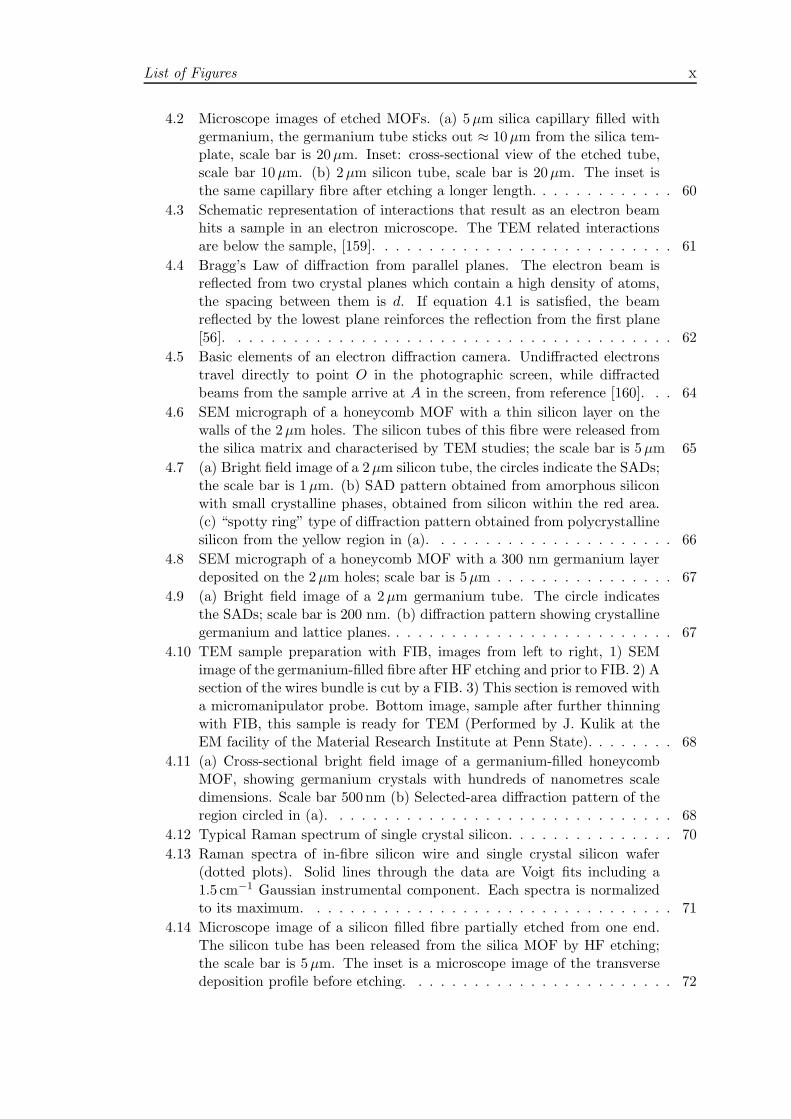
4.2 Microscope images of etched MOFs. (a) 5µm silica capillary filled withgermanium, the germanium tube sticks out ≈ 10µm from the silica tem-plate, scale bar is 20µm. Inset: cross-sectional view of the etched tube,scale bar 10µm. (b) 2µm silicon tube, scale bar is 20µm. The inset isthe same capillary fibre after etching a longer length. . . . . . . . . . . . . 60
4.3 Schematic representation of interactions that result as an electron beamhits a sample in an electron microscope. The TEM related interactionsare below the sample, [159]. . . . . . . . . . . . . . . . . . . . . . . . . . . 61
4.4 Bragg’s Law of diffraction from parallel planes. The electron beam isreflected from two crystal planes which contain a high density of atoms,the spacing between them is d. If equation 4.1 is satisfied, the beamreflected by the lowest plane reinforces the reflection from the first plane[56]. . . . . . . . . . . . . . . . . . . . . . . . . . . . . . . . . . . . . . . . 62
4.5 Basic elements of an electron diffraction camera. Undiffracted electronstravel directly to point O in the photographic screen, while diffractedbeams from the sample arrive at A in the screen, from reference [160]. . . 64
4.6 SEM micrograph of a honeycomb MOF with a thin silicon layer on thewalls of the 2µm holes. The silicon tubes of this fibre were released fromthe silica matrix and characterised by TEM studies; the scale bar is 5µm 65
4.7 (a) Bright field image of a 2µm silicon tube, the circles indicate the SADs;the scale bar is 1µm. (b) SAD pattern obtained from amorphous siliconwith small crystalline phases, obtained from silicon within the red area.(c) “spotty ring” type of diffraction pattern obtained from polycrystallinesilicon from the yellow region in (a). . . . . . . . . . . . . . . . . . . . . . 66
4.8 SEM micrograph of a honeycomb MOF with a 300 nm germanium layerdeposited on the 2µm holes; scale bar is 5µm . . . . . . . . . . . . . . . . 67
4.9 (a) Bright field image of a 2µm germanium tube. The circle indicatesthe SADs; scale bar is 200 nm. (b) diffraction pattern showing crystallinegermanium and lattice planes. . . . . . . . . . . . . . . . . . . . . . . . . . 67
4.10 TEM sample preparation with FIB, images from left to right, 1) SEMimage of the germanium-filled fibre after HF etching and prior to FIB. 2) Asection of the wires bundle is cut by a FIB. 3) This section is removed witha micromanipulator probe. Bottom image, sample after further thinningwith FIB, this sample is ready for TEM (Performed by J. Kulik at theEM facility of the Material Research Institute at Penn State). . . . . . . . 68
4.11 (a) Cross-sectional bright field image of a germanium-filled honeycombMOF, showing germanium crystals with hundreds of nanometres scaledimensions. Scale bar 500 nm (b) Selected-area diffraction pattern of theregion circled in (a). . . . . . . . . . . . . . . . . . . . . . . . . . . . . . . 68
4.12 Typical Raman spectrum of single crystal silicon. . . . . . . . . . . . . . . 70
4.13 Raman spectra of in-fibre silicon wire and single crystal silicon wafer(dotted plots). Solid lines through the data are Voigt fits including a1.5 cm−1 Gaussian instrumental component. Each spectra is normalizedto its maximum. . . . . . . . . . . . . . . . . . . . . . . . . . . . . . . . . 71
4.14 Microscope image of a silicon filled fibre partially etched from one end.The silicon tube has been released from the silica MOF by HF etching;the scale bar is 5µm. The inset is a microscope image of the transversedeposition profile before etching. . . . . . . . . . . . . . . . . . . . . . . . 72
List of Figures xi
4.15 Micro-Raman spectra of a silicon tube inside a MOF (top), silicon tubeetched out of the fibre template (middle), and a single crystal siliconwafer (bottom). The spectra were fitted with a single Voigt peak, in-cluding 1.5 cm−1 Gaussian instrumental broadening (solid lines). For in-fibre silicon the peak is centred at 517.5 cm−1 with 5.5 cm−1 FWHM. Theetched wire peak is at 519.6 cm−1 with 5.5 cm−1 FWHM, and the singlecrystal peak is at 520.1 cm−1 with 3 cm−1 FWHM. Each curve has beennormalized to the maximum of the peak. . . . . . . . . . . . . . . . . . . . 73
4.16 Raman data of a silicon tube removed from the MOF template. The insetshows the three Voigt peaks approximation (solid blue line through thedata). The red lines are the three decoupled peaks. Voigt peak 1 centredat 480 cm−1 is shown magnified 40× for clarity because it is sufficientlybroad and weak as to appear as nearly a straight line in the figure at thenormal figure scale. . . . . . . . . . . . . . . . . . . . . . . . . . . . . . . . 75
4.17 Raman spectra of silicon wires deposited at different temperatures, of T=450 C, 700 C, 750 C, and fibre annealed at 1450 C after deposition.The spectrum of single crystal silicon is included as a reference. EachRaman spectra is normalized to its maximum. . . . . . . . . . . . . . . . . 76
4.18 Raman spectra of silicon tubes deposited at 700 C and 450 C. Theblue plot through the data in the inset is the three Voigt approximationof the 700 C sample. The fitted is decoupled into three peaks, shownin red. Peak 1, located at 471.7 cm−1 with ∼ 86 cm−1 FWHM, peak 2at 507 cm−1 with FWHM of 13.88 cm−1 and peak 3 at 516.2 cm−1 with7.7 cm−1 FWHM. The high contribution of the amorphous peak to thespectrum indicates that the silicon is “just” begining to become crystallineat this deposition temperature. . . . . . . . . . . . . . . . . . . . . . . . . 77
4.19 Raman spectrum of silicon tubes deposited at 750 C. The blue linethrough the data in the inset is the three Voigt approximation of theRaman spectrum. Each decoupled peak is shown as a red line. Peak 1,located at 480 cm−1 with ∼ 81 cm−1 FWHM, peak 2 at 511.1 cm−1 withFWHM of 15.3 cm−1 and peak 3 at 516.4 cm−1 with 6.7 cm−1 FWHM. . . 78
4.20 Raman spectrum of a silicon tube annealed at 1450 C. Inset, the Ramandata was fitted by a single Voigt peak (blue line) including a 1.5 cm−1
Gaussian contribution. The peak is located at 516.86 cm−1 with a FWHMof 3.43 cm−1. Fitting with two or three peaks did not improve the r2 valueof the overall fitting. . . . . . . . . . . . . . . . . . . . . . . . . . . . . . . 79
4.21 Micro-Raman spectrum of a germanium tube inside a fibre and that ofgermanium single crystal wafer. Lines through the data are single Voigtfits including 1.5 cm−1 Gaussian component due to instrumental broadening. 80
4.22 A schematic view of a FET. In this model electrons are injected from thesource and collected at the drain. . . . . . . . . . . . . . . . . . . . . . . . 81
4.23 Schematic of in-fibre FET circuit diagram and microscope images of fibre’setched ends. The semiconductor core protrude out of the silica capillary. . 83
4.24 Cross section of both ends of a germanium fibre used for electrical char-acterisation, the sample is 11mm long. The semiconductor material fillscompletely the 5µm capillary hole. . . . . . . . . . . . . . . . . . . . . . . 84
List of Figures xii
4.25 Three-terminal electrical measurement on an 11mm long 5µm capillarycompletely filled with germanium. The Idrain vs Vgate characteristics areplotted. The transconductance (∂Idrain/∂Vgate) was measured to be ≈5 × 10⁻¹¹A/V, at Vsource = 10V. The inset shows the pinch-off behaviorof the device at Vgate ≈ −100V, at Vsource = 10V. The on-off operationratio of the FET is > 104. . . . . . . . . . . . . . . . . . . . . . . . . . . 84
4.26 Cross-sectional view of the silicon fibre used in electrical measurements,the sample is 18mm long. The silicon tube covers ≈ 50% of the 5µmcapillary hole area. . . . . . . . . . . . . . . . . . . . . . . . . . . . . . . . 86
4.27 Three-terminal electrical measurement on a 18mm length of a 5µm Si-filled capillary. The Idrain vs Vsource characteristics are plotted for differ-ent Vgate values. The transconductance (∂Idrain/∂Vgate) was determinedas being ≈ 1 × 10⁻¹²A/V, with Vsource = 20V. The inset shows howthe conductivity (+) and mobility (N) values of such a fibre change as afunction of temperature. The conductivity data is also fitted by a tech-nique of least squares to equation (4.12) (red line through the data). Thisapproximation yields a value of 3.3meV for the grain-barrier activationenergy (ε). . . . . . . . . . . . . . . . . . . . . . . . . . . . . . . . . . . . . 87
4.28 Microscope image of a 2µm capillary fibre filled with silicon. This fibrewas used in optical experiments. The cladding diameter is 125µm. . . . . 89
4.29 Transverse index profile of 2µm diameter silicon-filled MOF used in op-tical experiments. The red ring is a 600 nm silicon tube nSi = 3.46 at1.55µm. Silica is displayed with a pink colour with nSiO2
= 1.46. Theblack region is air nair = 1. . . . . . . . . . . . . . . . . . . . . . . . . . . . 90
4.30 Energy distribution of the first two guided modes supported by the sili-con fibre shown in Figure (4.29) as calculated by a full-vector imaginarydistance BPM. The red colour represents high power concentration whilethe pink regions are low concentration. The effective refractive index ofthe modes is written at the top of each image. . . . . . . . . . . . . . . . . 90
4.31 Near field image of the transmitted light through the 2µm silicon MOF. . 91
4.32 Schematic of light guiding experiment. (a) The end of a filled fibre isetched to completely expose 2mm of the central silicon core (blue) andtaper a portion of the silica cladding (red). (b) 633 nm light is guidedin the tapered silica cladding but not in the exposed silicon. (c) 1.55µmlight propagating through the same etched fibre. The light is scattered atthe end of the silica cladding but continues to propagate the full lengthof the silicon core. . . . . . . . . . . . . . . . . . . . . . . . . . . . . . . . 92
4.33 A germanium-broom: Bundle of 2µm diameter germanium wires ema-nating from a honeycomb MOF. Visible light propagation is prohibitedin germanium due to its high absorption at these wavelengths [17], pho-tograph by Neil Baril. . . . . . . . . . . . . . . . . . . . . . . . . . . . . . 93
4.34 Schematic diagram of an all-optical in-fibre light modulator. The probesignal at 1.55µm is guided by the fibre’s a:Si core. The pump pulsesexcite free carriers that change the optical properties of the silicon core,and modulate the amplitude of the probe signal (from reference [204]) . . 95
5.1 Lycurgus glass cup, demonstrating the bright red and green colours, intransmitted and reflected light of gold nanoparticles. Inset: scanning elec-tron microscopy (SEM) image of a characteristic nanocrystal embeddedin the cup’s glass, from the British Museum website [208]. . . . . . . . . . 97
List of Figures xiii
5.2 Plots of the dielectric function of a dielectric (left) and a free-electronmetal (right) calculated using the Lorentz relations (5.10) and Druderelations (5.14), respectively. The complex refractive index was obtainedusing equation (5.7). . . . . . . . . . . . . . . . . . . . . . . . . . . . . . . 102
5.3 Spectral dependance of the dielectric constant for (a) silver and (b) gold.The data was obtained experimentally by absorption and reflection mea-surements. All the experimental values of the dielectric constants of themetals used in this work are taken from [216] . . . . . . . . . . . . . . . . 103
5.4 SPPs on a metal-dielectric interface. (a) Schematic diagram of the chargeand electric field distributions at the interface. (b) The intensity of theelectric field which reaches its maximum at the surface and decays expo-nentially with distance away from it. (c) Curves showing the dispersionrelation of SPPs (plotted in blue), given by the real part of equation (5.15)and the dispersion relation of light propagating in the dielectric medium(red curve). The blue line is always lying below the light line indicatingthe non radiative nature of SPP modes. The grey arrow shows the mo-mentum mismatch, ∆kx, between the two waves at a certain excitationfrequency ωe. . . . . . . . . . . . . . . . . . . . . . . . . . . . . . . . . . . 104
5.5 Techniques used to couple light into surface plasmons. (a) Grating cou-pling geometry. (b) Kretchmann geometry, makes use of a high refractiveindex prism which is in contact with a metal surface. This method enablesexcitation of SPPs at the air/metal interface but SPPs at the metal/glassinterface cannot be excited. (c) Otto geometry, the metal surface is inclose proximity to the prism. . . . . . . . . . . . . . . . . . . . . . . . . . 106
5.6 Schematic representation of the interaction between a metal sphere and aplane wave. The sphere diameter is smaller than the wavelength of lightand thus, the charge distribution takes a dipole form. . . . . . . . . . . . 108
5.7 Extinction ratio for silver nanospheres, of different radii R as given byMie-Lorentz theory. . . . . . . . . . . . . . . . . . . . . . . . . . . . . . . 108
5.8 Solution of metallic nanoshells, as the shell thickness is increased theplasmon resonance is tunned from the visible to infrared wavelengths,taken from reference [243] . . . . . . . . . . . . . . . . . . . . . . . . . . . 109
5.9 (a) Commercially available plasmon sensors. Top: biosensor based onSPP resonances in smooth gold films, taken from reference [247]. Bottom:the high localization of EM fields at the surface of nanostructured metalfilm has been exploited for Surface Enhanced Raman Scattering sensing,from reference [260]. (b) Top: SEM image of silver nanostructure usedfor enhanced transmission experiments. Bottom: Image of transmittedlight, from reference [261]. (c) Top: SEM micrograph of a subwavelengthplasmonic Mach-Zehnder interferometer. Bottom: Near field image of thepropagating plasmon waves. Taken from reference [262]. . . . . . . . . . . 111
6.1 Diagram for Raman and Rayleigh scattering showing the energy levelsinvolved in the processes. Note that all the scattering processes in-volve a virtual state. Vibrational absorptions usually occur at infraredwavelengths while rotational absorptions occur in the microwave regime.Therefore, the energy difference (∆E) between two vibrational states ishigher than that between two rotational transitions. . . . . . . . . . . . . 114
List of Figures xiv
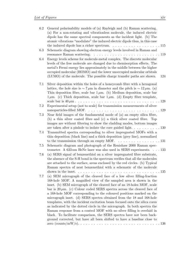
6.2 General polarisability models of (a) Rayleigh and (b) Raman scattering.(a) For a non-rotating and vibrationless molecule, the induced electricdipole has the same spectral components as the incident light. (b) Theatomic vibrations “modulate” the induced electric dipole thus, in this casethe induced dipole has a richer spectrum. . . . . . . . . . . . . . . . . . . 115
6.3 Schematic diagram showing electron energy levels involved in Raman andresonance Raman scattering. . . . . . . . . . . . . . . . . . . . . . . . . . 119
6.4 Energy levels scheme for molecule-metal complex. The discrete molecularlevels of the free molecule are changed due to chemisorption effects. Themetal’s Fermi energy lies approximately in the middle between the higheroccupied molecular (HOMO) and the lower unoccupied molecular orbitals(LUMO) of the molecule. The possible charge transfer paths are shown. 124
7.1 Silver deposition within the holes of a honeycomb fibre with a hexagonallattice, the hole size is ∼ 7µm in diameter and the pitch is ∼ 12µm. (a)Thin deposition fibre, scale bar 1µm. (b) Medium deposition, scale bar1µm. (c) Thick deposition, scale bar 1µm. (d) Empty fibre template,scale bar is 40µm . . . . . . . . . . . . . . . . . . . . . . . . . . . . . . . . 128
7.2 Experimental setup (not to scale) for transmission measurements of silvernanoparticles-filled MOF. . . . . . . . . . . . . . . . . . . . . . . . . . . . 129
7.3 Near field images of the fundamental mode of (a) an empty silica fibre,(b) a thin silver coated fibre and (c) a thick silver coated fibre. Topimages are without filtering to show the cladding modes, bottom imagesare taken after a pinhole to isolate the core guided light. . . . . . . . . . . 130
7.4 Transmitted spectra corresponding to silver impregnated MOFs with athin deposition (black line) and a thick deposition (grey line), normalizedto the transmission through an empty MOF. . . . . . . . . . . . . . . . . 131
7.5 Schematic diagram and photograph of the Renishaw 2000 Raman spec-trometer. A 633 nm HeNe laser was also used in SERS experiments. . . . 133
7.6 (a) SERS signal of benzenethiol on a silver impregnated fibre substrate,the absence of the S-H bond in the spectrum verifies that all the moleculesare attached to the surface, areas enclosed by the red circles. (b) TypicalRaman spectra of neat benzenethiol with a schematic of the moleculeshown in the inset. . . . . . . . . . . . . . . . . . . . . . . . . . . . . . . . 135
7.7 (a) SEM micrograph of the cleaved face of a low silver filling-fraction168-hole MOF. A magnified view of the sampled area is shown in theinset. (b) SEM micrograph of the cleaved face of an 18-holes MOF, scalebar is 20µm. (c) Colour coded SERS spectra across the cleaved face ofa 168-hole MOF corresponding to the coloured positions marked on themicrograph inset. (d) SERS spectra obtained from the 18 and 168-holetemplates, with the incident excitation beam focused onto the silica coresas indicated by the dotted circle in the micrograph. In both spectra theRaman response from a control MOF with no silver filling is overlaid inblack. To facilitate comparison, the SERS spectra have not been back-ground corrected, but have all been shifted to have a baseline close tozero (counts/mW/s). . . . . . . . . . . . . . . . . . . . . . . . . . . . . . . 136
List of Figures xv
7.8 Calculated mode profile of the 168-hole MOF showing (a) the fundamentalguided mode and (b) the cladding filling mode at an excitation wavelengthof 785 nm. The figures show the normalized power distribution across thesilica MOF as a function of radial position, as indicated by the dotted linesacross the 2D intensity plots shown in the top left insets. The top rightinsets show the distributed modes generated by launching a 633 nm laserinto the control silica (i.e. no silver) fibre as imaged by an Electrophysics7290A Vidicon IR camera. . . . . . . . . . . . . . . . . . . . . . . . . . . . 137
7.9 SEM micrographs (a) of the small core fibre template and (b) a silver-filledfibre, scale bars are 2µm in both images. . . . . . . . . . . . . . . . . . . 139
7.10 SERS spectra of aminothiophenol obtained from silver impregnated MOFs.(a) Spectra from small core MOF template and (b) from large MOF tem-plate. The blue spectra are obtained with the excitation laser focusedonto the silica cores. The spectra plotted in red are the signals obtainedwith the incident light focused onto the structured claddings. . . . . . . . 140
7.11 SERS signal of aminothiophenol obtained in a remote sensing configuration.141
7.12 Current/voltage measurements on various lengths of two 18-hole silverfilled MOFs with filling fractions of (a) ∼ 40% and (c) ∼ 10%. The sam-ples had been cleaved at the ends and electrical contacts made with InGaeutectic (circuit diagram in top inset of (a)). The lengths correspondingto each spectrum are given in the insets, together with the calculatedsample resistances based on an Ohmic model together with control mea-surements on an unfilled silica MOF (dashed lines). (b) and (d) displaythe corresponding SERS response of the different filling fractions shownin the micrograph insets. . . . . . . . . . . . . . . . . . . . . . . . . . . . 142
8.1 Photoluminescence of a series of different sized core-shell CdSe/ZnS quan-tum dots. All illuminated simultaneously with a hand-held ultravioletlamp. From reference [321] . . . . . . . . . . . . . . . . . . . . . . . . . . 144
8.2 Density of states as a function of energy of quantum-confined semiconduc-tor structures. As the degree of confinement increases the carriers occupyincreasingly fewer energy levels. QDs have a peak-like density of statesenabling a higher concentration of carriers to contribute to the band-edgeoptical material emission. This provides important applications for quan-tum systems, in principle, ultralow threshold laser diodes [328]. σ(E) andδ(E) denotes the step and Dirac-delta functions respectively. . . . . . . . 145
8.3 Schematic diagram of the experimental setup for colloidal synthesis ofPbSe QDs. The reactions take place in 3-necked flask with a Liebig con-denser attached to the middle neck and rubber septa for the introductionof reagents and a thermometer on the other two necks. The vessel isheated by a mantle, with temperature control via feedback. The entireapparatus is purged with nitrogen and kept at a slight overpressure byattaching the nitrogen line and a bubbler to the condenser. Inset photo-graph of the set-up. . . . . . . . . . . . . . . . . . . . . . . . . . . . . . . 148
8.4 The above graphs display the absorption of PbSe quantum dots from arepresentative synthesis for different growth times from 2 to 10 minutes,after injection. The plots show the absorption peak tuning as the particlesize (time) increases. The broadening of the absorption peak is mainlyrelated to inhomogeneous size distribution. . . . . . . . . . . . . . . . . . 150

List of Figures xvi
8.5 A two-level effective-mass model, predicting the variation in absorptionpeak wavelength with nanocrystal diameter, for spherical PbSe nanopar-ticles (see Appendix A). The parameters used in this model were Eg =0.28 eV, m∗(e) = 0.084m and m∗(h) = 0.70m, where Eg is the bulk band-gap energy and m is the electron rest mass. The inset shows a schematicband diagram for the 1S(e) and 1S(h) states of the PbSe quantum dot. . 151
8.6 Normalized room-temperature photoluminescence spectra of PbSe quan-tum dots from a representative synthesis for different growth times 3, 5,7 and 9 minutes after injection. The plots clearly show the size tuningof the PL peak with increased growth time. The QDs sizes were calcu-lated by the parabolic bands and effective mass approximation, using theposition of the absorption peak obtained in each experiment [335]. Thediameter was calculated to be D = 8.07 nm, D = 8.4 nm, D = 8.45 nmand D = 8.46 nm, respectively. The broadening of the features is due tolarger size distribution as the synthesis time increases. The graph alsoshows the absorption of the 3 min QDs for reference (blue line). . . . . . . 152
8.7 Absorption and photoluminescence spectra of the cyanine dye, indocya-nine green in DMSO are shown together with the PL spectrum of a rep-resentative synthesis of PbSe nanocrystals. In order to make a correct“photons out-photons in” calculation of the PL quantum yields, the ar-eas under the two PL spectra was calculate and the variations in detectorresponse and photon energy with wavelength was taken into account. . . . 154
9.1 (Left) Silicon-germanium radial heterojunction integrated into a 6µmMOF capillary, scale bar is 1µm. (Right) 80 nm thick gold layer se-quentially deposited onto a silicon tube, scale bar is 2µm. . . . . . . . . . 160
A.1 Views of important planes in a cubic Bravais lattice. The plane index isconventionally enclosed in parenthesis. The planes (100), (200), (1,0,0)are parallel to each other and perpendicular to the lattice vector ~a1. . . . 163
A.2 3D views of the crystal structure of silicon from two different angles. Theimage on the right also show the atomic bonds. The lattice constant ofsilicon is 5.43 A which is the distance between the atoms located in thecube vertices (white lines). The blue lines correspond to 2.35 A, fromreference [348]. . . . . . . . . . . . . . . . . . . . . . . . . . . . . . . . . . 164

List of Tables
3.1 Comparison of the physicochemical properties of liquids, supercritical flu-ids and gases. . . . . . . . . . . . . . . . . . . . . . . . . . . . . . . . . . . 43
8.1 Variation of the measured PL efficiency of PbSe as a function of thegrowth time. . . . . . . . . . . . . . . . . . . . . . . . . . . . . . . . . . . 154
xvii
Nomenclature and Abbreviations
e Electron charge, e = 1.602 × 10⁻¹⁹ C
c Speed of light, c = 2.998 × 10⁸ m/s
h Planck constant, h = 6.626 × 10⁻³⁴ J · s~ Reduced Planck constant, ~ ≡ h/2π
i Imaginary unit number, i =√−1
µ0 Vacuum magnetic permeability, µ0 = 4π × 10−7 H/m
ε0 Vacuum dielectric permittivity, ε0 = 8.85 × 10⁻¹² F/m
~E Electric field
~H Magnetic field
~D Electric flux density
~B Magnetic flux density
~J Current density
~r Spatial vector
t Time
ρ Charge density
σ Conductivity
τ Electron relaxation time
m Electron mass
υ Frequency
ω Angular frequency, ω = 2πυ
λ Wavelength
ε Dielectric permittivity, ε = ε1 + iε2
ǫ Relative dielectric permittivity, ǫ = ǫ1 + iǫ2
n Refractive index, n = n1 + in2
k Wave vector, k = k1 + ik2
TE Transverse Electric
TM Transverse Magnetic
ACS grade American Chemical Society grade
CVD Chemical Vapour Deposition
FET Field Effect Transistor
xviii
Nomenclature & Abbreviations xix
FIB Focused Ion Beam
HOMO Higher Occupied Molecular Orbital
HPCVD High-Pressure Chemical Vapour Deposition
IC Integrated Circuit
QD Semiconductor Quantum Dot
LSP Localized Surface Plasmon
LUMO Lower Unoccupied Molecular Orbital
MBE Molecular Beam Epitaxy
MOF Microstructured Optical Fibre
PBG Photonic Bandgap
PBGF Photonic Bandgap Fibre
PC Photonic Crystal
PCF Photonic Crystal Fibre
PVD Physical Vapour Deposition
TEM Transmission Electron Micrsocopy
TOP Trictylposphine
RRS Resonant Raman Scattering
SAD Selected Area of Diffraction
SC Supercritical
SCF Supercritical Fluid
SP Surface Plasmon
SPP Surface Plasmon Polariton
SERS Surface Enhanced Raman Scattering
SEM Scanning Electron Microscopy
VLS Vapour-Liquid-Solid

Acknowledgements
Firstly, I would like to thank my supervisor, Pier Sazio for introducing me to the field of
solid state physics, for all his effort put into this project, his continual guidance, advice
and for his friendship during the four years I have spent in Southampton. Further thanks
are given to my colleagues and friends, Anna Peacock and Chris Finlayson because
working close to them I have learned so many things from quantum dot’s fabrication
to plasmons physics. Both have played an important role in this work and have shared
with me many experimental challenges encountered in this exciting project. Thanks to
David Richardson for giving me advise and encouragement throughout my PhD.
My special thank to our outstanding research collaborators at Penn State: John Badding,
Venkat Gopalan, Don-Jin Won, Neil Baril, Jacob Calkins and Bryan Jackson who I had
the pleasure to work with, discuss so many aspects of this project and spent a great
time in State College! Their remarkable knowledge in high-pressure chemistry have
made possible the fabrication of the exciting fibres analyzed in this thesis. My thank
also extend to our collaborators from the University of Nottingham, Jixin Yang and
Steve Howdle for producing the silver fibres I have used during this work.
I wish to thank Lencho, Anna, Pier and Eleanor who have had the “great pleasure” of
proof reading this thesis. Thanks for all your constructive suggestions and corrections!
I would also like to extend my gratitude to my officemates and other members of the
Optoelectronics Research Centre, especially to Naveed, Symos, Francesca, Lionel, Ever-
ardo, Rodrigo and Laura, for sharing their equipment with me and for many interesting
discussions on optoelectronics and the PhD life. . .
I want to express my gratitude to my sponsor, CONACyT (National Council for Science
and Technology of Mexico) who made it possible for me to spend these four years in the
Optoelectronics Research Centre with all its advantages, excellent laboratories, traveling
to conferences, interesting lectures, great people, etc.
Many friends in Southampton should be thanked for providing me the essential laugh,
support and the entertainment needed to reach this point: Catia, Arturo, Vladis, Jorge,
xx

Andy, Steve, Maria & Rob, David & Rocio, Eli, Nav, Symos and Greg thanks to you
all !!
28 years ago, Paty and Miguel gave the first step in this story... A very especial thanks
go to you for giving me love, trust, friendship and teaching me good values that have
helped me to fulfil this and many other goals... you have always been my best teachers!
I cannot forget my twin brother, Rodrigo who I know since time before I was born...
and some years after Mariano was there... thanks to you both for sharing this story with
me.
To all my family, thanks for your love, support and encouragement!
As well a big “thank you!” to my friends Lencho, Mad, Mauricio, Gustavo, Joaquin,
Rogelio, Andres for many years of unbroken friendship.
Finally, my sincerely thank to you Helene, my biggest happiness was to meet you and
share this time with you.
xxi

A Paty y Miguel
“The known is finite, the unknown infinite; intellectually we stand
on an islet in the midst of an illimitable ocean of inexplicability.
Our business in every generation is to reclaim a little more land. . . ”
Thomas H. Huxley
xxii
Chapter 1
Introduction
21st Century global telecommunications systems have been made possible thanks to
optical fibre technology. Optical fibres are the internet and telephone communications
backbone, interconnecting buildings, cities and continents. Around the world, lie more
than 300 million [1] kilometres of fibre that can carry millions of simultaneous phone calls
and the Internet’s information. A significant portion of the development of optical fibres
for telecommunications took place at the University of Southampton, with its origins
going back as far as the 1960’s. These innovations led directly to the data communica-
tions revolution of the late 20th century and have now impacted many other technologies
from remote sensing to biomedicine. In addition, the invention of the transistor in 1947
at Bell Labs gave birth to the last century’s semiconductor revolution which has marked
a new technological age in human history. As a result, electronic and optoelectronics
planar devices based on silicon, germanium and compound semiconductors have had a
profound effect on our way of living.
Currently, optical telecommunication systems combine silica optical fibres as signal car-
riers with external optoelectronics semiconductor circuits that are capable of generating,
detecting, and manipulating the light. However, the process of converting the photons
to electrons requires coupling optics, alignment structures and packaging. These con-
version processes consume enormous amounts of power, require costly technology and
have limited the overall bandwidth of optical systems. Therefore, it would be ideal not
to transform in-fibre photonic signals to chip-based electronic signals, due to the com-
plexity of having to use heterogeneous and discrete optoelectronic components. Indeed,
the ultimate vision would be purely fibre based devices in which photons do not need to
leave the fibre. One example of such a device is the erbium-doped-fibre-amplifier (EDFA)
which replaced old heterogeneous optoelectronic amplifiers composed of photo-detectors,
filters, electronic amplifiers and lasers diodes to reconvert the amplified electronic signal
back again into photons, with a single all-optical amplifier. Due to the amplifier’s in-fibre
1
Chapter 1. Introduction 2
nature they allow optical systems to operate with a broad bandwidth. These systems
were commercialized in the late 80’s and have become widely used in the telecommuni-
cations industry and for laser machining applications.
Although, the EDFA has solved the problem of how to amplify optical signals, the sig-
nal processing involved in the transmission system is still carried out in the electronic
domain, which limits the overall bandwidth and raises the costs of the optical networks.
The ability of solid-state devices to manipulate electrons and photons relies on the mi-
croelectronics industry’s exceptional capability of integrating semiconductor, dielectric
and conductive materials in a single device. However, until now, fibre technology has
not been able to integrate crystalline semiconductors and metals with anywhere near
their level of sophistication.
It has been well known for many years that the periodic organization of atoms within
a crystalline medium gives rise to different electronic bands in which the conduction
of electrons is forbidden. Electrons with energy in between the valence band and the
conduction band are not allowed to exist in semiconductor crystals. Utilizing these
electronic bandgaps to control the propagation of electrons led to the microelectronics
revolution of the last century and is now giving birth to the nanosciences and integrated
photonics. However, it was not until 1987, when Eli Yablonovitch [2] and Sajeev John [3]
proposed, independently, that the fabrication of materials with periodic dielectric struc-
tures on a scale comparable to the wavelength of light, offers the possibility of tailoring
the way light propagates within materials, in the same manner that ordered arrangement
of atoms do for electron waves. These novel structures are known as photonic crystals
(PCs). In photonic crystals, the periodic index difference can give rise to photonic
band gaps (PBGs) where propagation of electromagnetic waves would be prohibited for
certain wavelengths [4] even though the constituent (bulk) dielectrics are intrinsically
transparent. Such periodic dielectric structures have numerous potential applications
in the development of photonics devices which offer control over the electromagnetic
fields and the possibility of manipulating photons with unprecedented optical degrees of
freedom [5, 6, 7].
Standard optical fibre’s operation usually relies on a physical mechanism named total
internal reflection or index guiding, where light propagates within a higher refractive
index core surrounded by a lower index cladding. During more than 40 years of research
on index guiding optical fibres, the full capabilities of silica-doped fibres have almost
been reached. Most of the development over this time was mainly focused on reducing
the fibre propagation loss. The discovery of photonic crystals has been very promising
for optical fibre technology. In 1995 Russell [8] proposed the concept of a novel class
of optical fibres with a photonic crystal cladding to confine the light within the fibre
core. A year later, a photonic crystal fibre (PCF), single material fibre that has a

Chapter 1. Introduction 3
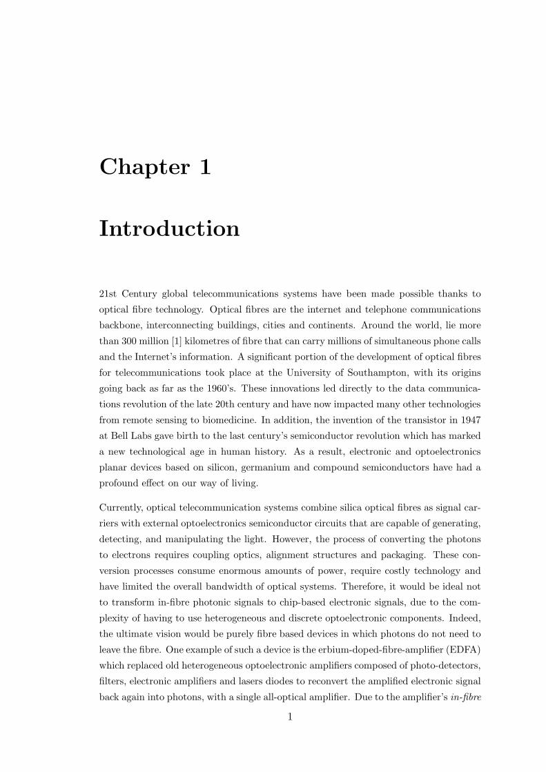
Figure 1.1: SEM cross sectional micrographs of different microstructuredoptical fibres fabricated at the ORC. The central fibres are among the mostadvanced kind of MOFs as they can guide light in their hollow core by photonic
band gap mechanisms.
silica core surrounded by a cladding with a periodical arrangement of air holes running
down its length was fabricated [9]. This fibre guided light by a modified total internal
reflection mechanism [10]. However, it was not until 1998 that the first true photonic
bandgap fibre (PBGF) was created [11]. Both kinds of fibres can be considered as
microstructured optical fibres (MOFs). MOFs are usually single material optical fibres
with air-holes that define their transverse profile. Their capillary voids can be precisely
configured in a variety of structures and with diameters ranging from tens of nanometres
to a few microns (Figure 1.1). Solid MOFs in which the air holes are replaced by different
kind of glasses can also be fabricated. MOFs had already demonstrated advantages over
conventional silica-doped fibres due to their novel optical properties such as broad band
single mode guidance, widely engineerable dispersion, nonlinear properties, mode area
tailoring and photonic band gap guidance in air [12, 13, 14, 15].
The most interesting property of MOFs, for the research presented here, is that they
have holes which provide a way to infiltrate other materials into the fibre. Our research
group has recently demonstrated that silica fibres combining dielectrics, metals and
crystalline semiconductors can be fabricated by new material deposition processes similar
to those used in the planar microelectronics industry [16, 17]. This technology may lead
to novel multifunctional optical fibres capable of not only guide light but also able
to generate, manipulate and process optical and electronic signals. Furthermore the
formation of semiconductor tubes and wires within nanoscale holes of MOFs will bring
together fibre optics technology with the growing field of ultra small semiconductor
Chapter 1. Introduction 4
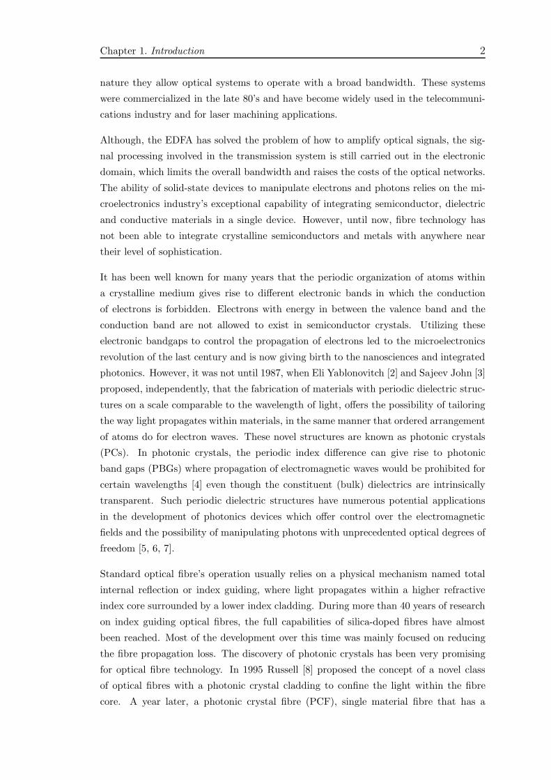
nanowires [18, 19, 20, 21, 22]. Figure 1.2 is an artistic vision of the integration of
solid-state and fibre technologies.
Figure 1.2: The deposition of semiconductors and metals within the capillaryholes of microstructured optical allow for the fusion of two powerful technologies:semiconductor and microstructured optical fibres technologies for the creation ofa new class of metamaterials. This gives room for the development of interesting
in-fibre electronic, optoelectronic and plasmonic devices.
1.1 Past and Current Work
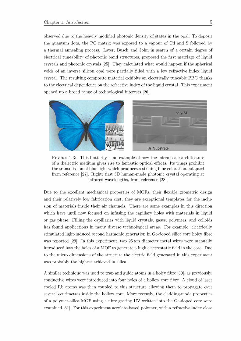
Although the flow of light using micro/nanoscale structures was mastered by nature
many millions of years ago (Figure 1.3), it was not until the past two decades when
the refinement of micro/nano materials fabrication techniques allowed the development
of artificial photonic crystal structures. The first photonic crystal was fabricated by
mechanically drilling millimetre sized holes into a dielectric material [23]. It presented a
complete 3D photonic band gap for microwave frequencies. The realisation of this first
photonic crystal gave rise to increasing scientific and technological interest especially in
the optical regime. Photonic crystal technology has matured at a surprising pace and
research has gradually shifted focus from the fundamental physics of the properties of
these materials to more application driven research and devices. Nowadays, photonic
crystal technology is thought to be one of the future platform technologies to create
optical microcircuits capable of processing speeds potentially much faster than today’s
microelectronic circuits.
The precise periodic nature of these mesoporous structures readily lends them to the
concept of embedding functional materials into the void lattice spaces. This enables them
to combine the optical properties of the original structure with the optical or electronic
functionality of the embedded materials. In this section the significant advances on
depositing materials inside photonic crystals are reviewed. One can start by mentioning
the work by Vlasov and colleagues, who embedded CdS quantum dots (QDs) into the
lattice voids of an inverse opal [24]. A drastic change in the QDs emission spectra was
Chapter 1. Introduction 5
observed due to the heavily modified photonic density of states in the opal. To deposit
the quantum dots, the PC matrix was exposed to a vapour of Cd and S followed by
a thermal annealing process. Later, Busch and John in search of a certain degree of
electrical tuneability of photonic band structures, proposed the first marriage of liquid
crystals and photonic crystals [25]. They calculated what would happen if the spherical
voids of an inverse silicon opal were partially filled with a low refractive index liquid
crystal. The resulting composite material exhibits an electrically tuneable PBG thanks
to the electrical dependence on the refractive index of the liquid crystal. This experiment
opened up a broad range of technological interests [26].
Figure 1.3: This butterfly is an example of how the micro-scale architectureof a dielectric medium gives rise to fantastic optical effects. Its wings prohibitthe transmission of blue light which produces a striking blue coloration, adaptedfrom reference [27]. Right: first 3D human-made photonic crystal operating at
infrared wavelengths, from reference [28].
Due to the excellent mechanical properties of MOFs, their flexible geometric design
and their relatively low fabrication cost, they are exceptional templates for the inclu-
sion of materials inside their air channels. There are some examples in this direction
which have until now focused on infusing the capillary holes with materials in liquid
or gas phase. Filling the capillaries with liquid crystals, gases, polymers, and colloids
has found applications in many diverse technological areas. For example, electrically
stimulated light-induced second harmonic generation in Ge-doped silica core holey fibre
was reported [29]. In this experiment, two 25µm diameter metal wires were manually
introduced into the holes of a MOF to generate a high electrostatic field in the core. Due
to the micro dimensions of the structure the electric field generated in this experiment
was probably the highest achieved in silica.
A similar technique was used to trap and guide atoms in a holey fibre [30], as previously,
conductive wires were introduced into four holes of a hollow core fibre. A cloud of laser
cooled Rb atoms was then coupled to this structure allowing them to propagate over
several centimetres inside the hollow core. More recently, the cladding-mode properties
of a polymer-silica MOF using a fibre grating UV written into the Ge-doped core were
examined [31]. For this experiment acrylate-based polymer, with a refractive index close
Chapter 1. Introduction 6
to that of silica, was introduced into the air regions (six 40µm diameter air holes) by
placing one end of the fibre into low viscosity uncured polymer, and connecting the
other end of the fibre to low vacuum. Once the polymer was inside the fibre holes, it
was cured with UV light. Using the thermo-optical response of the polymer the authors
demonstrated a reduction of the cladding-modes. Later Kerbage et al. used the same
procedure to incorporate polymer into the air hole regions of a tapered air-silica MOF
[32]. By taking advantage of the refractive index temperature response of the polymer
and the high interaction between the light and the polymer in the tapered length, they
demonstrated an integrated all-fibre variable attenuator. Another inventive example
took advantage of the existence of air holes in MOFs to fabricate an in-fibre Mach-
Zehnder interferometer [33]. For this trial, an eutectic metal alloy, with low melting
temperature, was introduced under 8 atm pressure into a twin core optical fibre which
also had two parallel 20µm holes running next to one core. The high interaction between
light and the electric field generated between the electrodes achieved a 1.4 kV switching
voltage from the weak intrinsic Kerr nonlinearity of silica, this fibre is shown in Figure
1.4a. Soon after, Larsen and collaborators demonstrated thermo-optic switching of
visible light propagating in a photonic bandgap fibre whose holes were impregnated
with liquid crystal. In this experiment the 3.5µm diameter holes of a photonic crystal
fibre were filled with high refractive index liquid crystal [34]. To access the potential
of controllability, the fibre was coated with a thin conductive layer that worked as a
resistive micro-heater to thermally change the optical properties of the liquid crystals.
The resulting photonic crystal structure has narrow photonic bandgaps crossing the
silica line, thus the PBG allows for certain frequencies to propagate in the low-index
silica core. By changing the temperature of the liquid crystal, the photonic bandgap
may be tuned from green to blue, and in this way the authors fabricated the first thermo-
optic fibre switch based on PBG effects. More recently, gas-filled hollow core photonic
bandgap fibres were used as compact and high performance Raman lasers [35, 36]. The
stable performance of these compact fibre devices may find applications in high-precision
frequency measurements, quantum optics and nonlinear optics. Several other device
applications including fibre sensors have been demonstrated by filling MOF capillaries
with different fluids and colloids.
The most noteworthy example of a MOF combining different materials was recently
demonstrated by Bayindir and colleagues, who fabricated MOFs that combine solid
state materials [37]. Their approach entails the drawing of fibre preforms which include
low melting temperature metals, amorphous semiconductors, and a high-glass-transition-
temperature polymeric insulator. The resulting fibre can be used to construct detectors
which are sensitive to illumination along the entire fibre length. Figure 1.4b shows a
SEM micrograph of one of these hybrid fibres. These kinds of MOFs were drawn with all
components present in the fibre preform, therefore the technique requires all materials
Chapter 1. Introduction 7
Figure 1.4: (a) Example of a MOF filled with Bi and Sn metal eutectic. Themelting temperature of the eutectic is 137 C and the pressure used to introducethe liquid metal into the 20µm fibre holes was 8 atm. The resulting fibre wasused as a Mach-Zehnder amplitude modulator, from reference [33]. (b) Cross-sectional SEM micrograph of a hollow-core metal-semiconductor-insulator fibre.The upper inset shows the omnidirectional mirror which is formed by an arrayof quarter-wave As2Se3 and PEI layers. Also a metallic, Sn, filament which isused as the conductive medium of the in-fibre detector is shown in the inset.The lower inset is a picture of 1 m long, 1 mm thick hybrid fibre, taken from
reference [37].
to have similar melting temperatures and thermal expansion coefficients. Thus the
number of possible materials that can be used to construct dielectric, semiconductor
and conductor impregnated MOFs using this technique is limited. In addition, there
have been some experiments demonstrating the deposition of solid-state materials inside
capillaries using conventional chemical deposition processes [38]. But because of mass
transport constraints along high aspect ratio structures these studies have been restricted
to capillaries bigger than 10µm.
All the previous experiments exemplify the advantages of introducing functional materi-
als within MOFs capillaries. Especially, the inclusion of semiconductors and metals into
the air channels of MOFs lead to a number of exciting in-fibre device applications, such
as the fibre fabricated by Bayindir et al. [37]. This could also generate a brand new class
of fibre devices capable of generating light, controlling it and also able to create fibre
sensors with a high sensitivity. Clearly, however, the methods that have until now been
used to deposit materials into holey fibres, suffer from disadvantages such as materials
inflexibility, they can only be applied to fluids and are restricted to large holes.
Supercritical fluid (SCF) deposition and high pressure synthesis techniques have been
successfully addressed to deposit high melting temperature semiconductors such as: sili-
con [39] and germanium [40] nanowires within mesoporous silica templates. Also, metal
deposition from organometallic compounds in supercritical carbon dioxide (scCO2) has
also been widely used to generate homogeneous metal films into mesoporous substrates
(e.g. gold [41], copper, nickel [42] and platinum [43]). Because of the deposition flexibil-
ity of high pressure methods and supercritical fluids, our research group has investigated

Chapter 1. Introduction 8
these new deposition techniques to enable the impregnation of solid state materials in-
side optical fibres using pressures in the range of 2− 100MPa, which are well sustained
by the intrinsic strength of fused silica fibres (which is greater than 1GPa [44]). For
those who are not familiar with high pressure systems is interesting to mention that
the pressure used in the experiments is equivalent to the water pressure hundreds to 10
thousand metres below sea level!
Figure 1.5 shows an example of an empty MOF impregnated with silicon via a high pres-
sure method that was developed in this work. Our research group has also demonstrated
the deposition of amorphous and crystalline germanium, single crystal silicon, metals:
silver, gold, inside silica MOFs [16] with capillaries as small as 100 nm in diameter and
for tens of centimetres length. The number of materials that can be deposited by these
techniques is thus not limited by their melting temperature and so complex fibre based
devices can be envisioned.
Figure 1.5: (a) Empty air silica MOF template, the scale bar in the inset is2 µm. Despite the fragile appearance of the thin ( < 100 nm) capillary walls,this figure illustrates how robust these fibres are. MOF are able to supportthe high precursor pressure required for the deposition process. (b) Conformaldeposition of polycrystalline silicon within the MOF holes using a high pressure
material deposition technique, the scale bar is 1 µm.
1.2 Thesis Structure
As described in this chapter, the work in this thesis is related to the use of microstruc-
tured optical fibres as templates for micro/nano materials fabrication. It comprises a
collection of experiments involving the deposition of semiconductors, metals and poly-
mers within the capillary holes of MOFs. The resulting fibres have proved optical guid-
ance and relevance as molecular sensors. This research is part of a joint research effort
between the Optoelectronics Research Centre at the University Southampton, the Penn-
sylvania State University Materials Research Institute and the University of Nottingham
Supercritical Chemistry group. This close multidisciplinary effort shares expertise in fi-
bre design and fabrication, together with high pressure chemistry for the deposition

Chapter 1. Introduction 9
of functional materials, including semiconductors, metals and polymers, into the struc-
tures; as well optical, material and chemical characterization studies of the resulting
fibres. Silica MOFs are first fabricated in the ORC, then the deposition of materials
inside the fibres holes is done in PSU and in Nottingham Universities. Finally, most of
the fibre characterisation presented in this thesis was done here in Southampton.
Chapter 2 provides an introduction to MOFs including their optical properties and
current computational methods used for their calculation. It also shows a description of
the stack-draw technique used for the fabrication of silica MOFs. During the first year of
his PhD studies the author was involved in the drawing of silica capillaries and MOFs.
Effort was put on the characterisation of the fibre structure via SEM studies and on
the fabrication of fibres with nanoscale features. After the fire in the ORC clean rooms
in November 2005 no further fibre fabrication was carried out by the author. In this
chapter, the author uses a commercial software based on full-wave plane-wave expansion
method to theoretically study the bandgap structure of semiconductor-modified MOFs.
Unfortunately the programs developed for this task and most of the results obtained
were lost in the fire.
Chapter 3 introduces the different methods currently used in microelectronics and nanofab-
rication for the deposition of semiconductors, metals and dielectrics within planar and
3D substrates. Their experimental advantages, disadvantages and possible extension
to MOF deposition are discussed. The chapter closes with a description of novel high
pressure deposition techniques developed during this project for the formation of crys-
talline semiconductor, metal and polymeric tubes within MOFs templates. The material
deposition is carried out by our research collaborators in PSU and Nottingham. The
Southampton team visited the PSU team in two occasions and during these visits the
author fabricated several silicon and germanium fibres. The author carried out SEM
studies of the impregnated fibres in order to characterise their deposition profile.
Chapter 4 details the characterisation methods used to obtain the structural, optical
and electrical properties of silicon and germanium-filled MOFs. A key requirement for
the characterisation of semiconductor modified MOFs is to expose the semiconductor
material from the silica cladding. The author designed and made the tools required for
the HF etching and investigated the experimental conditions required to achieve a precise
control over the etching process. The samples used for the first TEM studies presented
in this chapter were fabricated and prepared by the author in PSU. Afterwards, the
second and more advanced TEM analysis presented in this chapter was done by our
collaborators in PSU. This chapter also show Raman studies of silicon and germanium
MOFs, the majority of the semiconductor fibres and Raman experiments were carried
out by the author. The demonstration of the first electronic device inside an optical
fibre is presented in this chapter. Some of the semiconductor fibres used for electrical
Chapter 1. Introduction 10
measurements were fabricated by the author. The electrical measurements presented in
this chapter were done in collaboration with other members of the group. As the etching
process was done in the ORC clean rooms, the fire also affected this part of the project
and it was not possible to fabricate new devices after November 2005.
Chapter 5 describes the field of plasmonics. It concentrates on details of the optical
properties of metals and provides a theoretical background to the following two chapters.
Metallo/dielectric nanostructures, which allow the excitation of plasmons, have opened
up new possibilities for Raman scattering as a powerful spectroscopy technique, and are
described in Chapter 6. In the search for an application of metal-modified MOFs, this
chapter explains the nature of the Raman effect and provides the theoretical background
of Surface Enhanced Raman Scattering (SERS).
The experimental SERS results obtained using silver modified MOFs are presented in
Chapter 7. MOFs SERS substrates provide an interesting method for the fabrication
of inexpensive and powerful molecular sensors. The silver-modified MOFs used in these
experiments were fabricated by our collaborators in Nottingham and all the experiments
presented in this chapter were done by the author.
Chapter 8 begins by outlining the synthesis of PbSe quantum dots performed by a team
consisting of members of the Southampton Chemistry department, as well as the author
and other members of the group. The following section will then present the optical
properties of semiconductor quantum dots. The absorption and photoluminescence ex-
periments presented in this chapter were carried out by the author and other members
of the group.
Chapter 9 is a summary of results and discusses the future directions that will follow
from the research presented in this thesis.

Chapter 2
Microstructured Optical Fibres
Firstly, in order to avoid confusion, it is important to point out that microstructured
optical fibres are also referred as photonic crystal fibres (PCF) and holey fibres. Since the
original motivation for developing these fibres was the creation of structures that able
to guide light by means of a 2D photonic bandgap the term photonic crystal fibre was
introduced. In a large part of literature this term is used to refer to all types of fibres
with microscale features defining their transverse profile. However, as these fibres not
necessarily have a periodic arrangement of holes and can guide light by both photonic
bandgap effects and modified internal reflection, the more general term microstructured
optical fibre is preferred in this thesis. The following chapter presents a comprehensive
review of the optical properties, guidance mechanisms, modelling methods and fabrica-
tion methods of MOFs.
2.1 History of MOFs
A remarkable property of microstructured optical fibre (MOF) manufacture, is that the
continuity of air channels running along the length of a glass preform are preserved when
drawn down to the micro-scale. This property was investigated back in the early 70s
by Kaiser et al. [45, 46]. They fabricated a single-material fibre consisting of a small
diameter rod supported by thin glass struts inside a larger tube (Figure 2.1a). In 1977,
Yariv et al. [47] theoretically proposed a fibre with a periodically structured cross-section
which could guide light in a low refractive index core due to Bragg reflections that prevent
light dissipation in the cladding. However, most of the research in fibre technology
in those years was focused in reducing transmission loss. With the implementation
of chemical vapour deposition (CVD) techniques to fibre fabrication, in the late 70’s
the loss of conventional step-index fibres was reduced to lower values [48] than those
11
Chapter 2. Microstructured Optical Fibres 12
achieved with MOF technology, and so, MOF research was left aside for many years. It
was not until the seminal work of Russell and co-workers [9], in 1996, that the interest in
microstructured optical fibres was renewed. They fabricated a single material fibre which
contained a periodic arrangement of air holes that ran along the fibre length and the fibre
core was formed by replacing the central hole with a solid region, (Figure 2.1b). As the
purpose of this fibre was to confine and guide light due to photonic bandgap effects, they
introduced the term photonic crystal fibre. However, the fibre structure was not regular
enough and the holes were not large enough to support photonic bandgap guidance [10].
Since then photonic crystal fibres (PCF), with a periodic or aperiodic transverse mi-
crostructure, have been used as practical fibre waveguides. After the success of PCF
technology, many kinds of structures with periodically structured cross-section have been
fabricated. For example, the Bragg fibres proposed in the 70s are currently produced by
many different methods. In 2000, Brechet et al. [49, 50] made a solid core Bragg fibre
using modified-CVD. In addition, employing a combination of polymer and chalcogenide
glass, Joannopoulos’ group at MIT in the US has realized a hollow-core version of Bragg
fibres [51, 52, 53].
In a conventional optical fibre the light propagation is due to total internal reflection at
the core/cladding interface and light is confined in the core due to its higher refractive
index than that of the cladding. In contrast to this, MOFs are able to guide light by
means of two different mechanisms: Modified total internal reflection, in which light is
guided in a solid core, surrounded by a (not necessarily periodic) structured cladding. In
this case the average refractive index of the cladding is decreased because of the air holes
(low refractive index). This ensures that light incident at certain angles propagates in
the high refractive index core by modified total internal reflections at the core/cladding
interface, as in conventional optical fibres [9]. On the other hand, photonic bandgap
fibres are an especial category of MOFs which exploit the photonic bandgap effects as
the mechanism of light guidance therefore they can guide light in a low refractive index
medium [11]. In photonic bandgap fibres (PBGFs) the air holes that define the cladding
region are arranged on a periodic lattice which presents a photonic band gap that does
not allow light to propagate in the cladding region. By breaking the order of the cladding
i.e. adding a defect in the structure it is possible to introduce localized modes within
the defect. This is typically done by introducing a hollow core in the centre of the
structure. If light can propagate in the defect but its frequency lies within a bandgap
it will not be allowed to propagate in the cladding and therefore the optical energy
will be concentrated in the defect. Hollow-core PBGF are a special class of bandgap
fibres that guide light in a central air core [54]. The design freedom of MOFs has
allowed new opportunities in optical fibre technology. Over the past few years they have
shown potential for many applications and have permitted progress in several areas such

Chapter 2. Microstructured Optical Fibres 13
as medical sciences, nonlinear optics, telecommunications, supercontinuum generation,
high power delivery and sensors.
Figure 2.1: (a) First demonstration of a MOF, taken from reference [45]. (b)First MOF with a silica core surrounded by a periodic array of air holes in silica,
from reference [9].
2.2 Fabrication of MOFs
Microstructured optical fibre fabrication typically involves two stages: preform fabrica-
tion and fibre drawing. A preform is a centimetre-scale replica of the fibre normally
∼ 50 cm in length and ∼ 20mm in diameter. After fabricating the MOF preform it is
drawn down to micro-scale dimensions on a fibre drawing tower. Figure 2.2 shows the
schematic preforms of a solid and hollow core MOFs. During the relatively short history
of MOF technology various preform synthesis methods have been developed to allow the
fabrication of a variety of fibre structures. There are many examples of preform fabrica-
tion including stacking of capillaries and rods, sol-gel casting, direct drilling, extrusion
from bulk glass with low softening temperature and rolling flexible material sheets into
tubes, each of which has advantages and disadvantages depending on the glass used and
the desired fibre geometry. The most commonly used technique is capillary stacking
which is especially flexible for silica MOFs fabrication. This method involves stacking
glass capillaries and rods of ∼ 1mm diameter inside a silica tube with an internal di-
ameter of ∼ 20mm. These capillaries are drawn from a starting tube of high-purity
silica with an outer diameter of 10 − 20mm. The inner/outer diameter of the starting
tube determines the ratio between the hole diameter and the lattice pitch in the drawn
fibre. All the silica MOFs preforms used in the present work have been fabricated by
this method. The resulting preform is then drawn into either a fibre or cane. If very
small features (< 2µm) are required then a two step drawing process is used. The mi-
crostructured cane from the first draw is introduced into a silica tube and is then drawn
into a fibre.

Chapter 2. Microstructured Optical Fibres 14
Figure 2.2: Top, examples of (a) solid core and (b) air core MOFs preformsfabricated by stacking silica capillaries and rods. Bottom, SEM micrographs of
the MOFs which have the same geometry as their preform.
A 5m fibre tower, whose schematic is shown in Figure 2.3, was used for MOF drawing.
The preform is mounted in a holding chuck attached to a feed mechanism that lowers
the preform into a furnace at the feeding speed (Vp). The furnace temperature is raised
to 1900 C − 2000 C and the drawn fibre is taken up by the capstan which controls
the draw speed (Vf ). In order to maintain a uniform fibre outer diameter, the drawing
process includes a diameter monitor which is located at the furnace exit. Before the
fibre reaches the capstan it is coated with a protective polymer. Coating is required
to protect the pristine silica surface from scratches and abrasion and it preserves the
intrinsic strength of silica. The acrylate coating is applied in liquid phase and is solidified
by UV-curing. Silica MOF fibres fabricated by this method have extremely high tensile
strength (more than 1GPa [44]) which makes them excellent reaction vessels for high
pressure deposition experiments.
Due to the potential importance of having MOFs and silica capillaries with nanoscale
dimensions for nanomaterial templates, several experiments were carried out in order to
control the fibre’s hole size in the nanoscale regime. The preform feed speed, Vp, the
furnace temperature and the drawing speed, Vf are the main parameters in determining
the fibre structure. In these experiments the diameter monitor was used to measure
the external diameter, which for our experiments is not necessarily 125µm as it is for
standard fibres. The dimensions of the fibre channels were measured under an optical
microscope as the fibre was drawn. Although the desired subwavelength features could

Chapter 2. Microstructured Optical Fibres 15
Figure 2.3: Schematic diagram for a drawing tower.
not be resolved using the optical microscope, in most of the cases it was possible to
determine whether the holes had collapsed or the subwavelength capillary holes were
preserved. The drawing parameters were then varied and new fibre samples were taken.
SEM micrographs indicated that it was possible to fabricate MOF with internal dimen-
sions < 500 nm as well as silica capillaries with an inner diameter as small as 100 nm.
Figure 2.4 shows a honey-comb fibre which was drawn down to the nanoscale, it is pos-
sible to appreciate that by changing the drawing conditions the holes size was changed
from ∼ 450 nm to 250 nm. It is important to note how precisely the hole size can be
controlled. These results have shed light onto the application of MOFs in nanotechnol-
ogy which has been hardly explored before. In the next chapter we move forward into
the formation of semiconductor nanotubes within the nanoholes of MOFs.
2.3 Fundamentals of Photonic Crystals
Photonic bandgap (PBG) materials give new opportunities in quantum optics, nonlinear
optics and optoelectronics. These structures were predicted theoretically to describe two
new optical principles, the localization and trapping of light in a PC [3, 55] and the com-
plete inhibition of spontaneous emission [2]. Maxwells’ equations are the fundamental
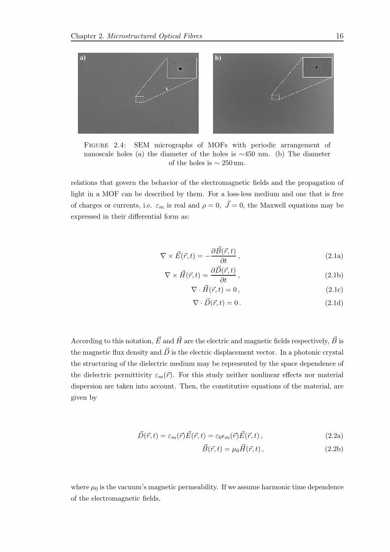
Chapter 2. Microstructured Optical Fibres 16
Figure 2.4: SEM micrographs of MOFs with periodic arrangement ofnanoscale holes (a) the diameter of the holes is ∼450 nm. (b) The diameter
of the holes is ∼ 250 nm.
relations that govern the behavior of the electromagnetic fields and the propagation of
light in a MOF can be described by them. For a loss-less medium and one that is free
of charges or currents, i.e. εm is real and ρ = 0, ~J = 0, the Maxwell equations may be
expressed in their differential form as:
∇× ~E(~r, t) = −∂~B(~r, t)
∂t, (2.1a)
∇× ~H(~r, t) =∂ ~D(~r, t)
∂t, (2.1b)
∇ · ~H(~r, t) = 0 , (2.1c)
∇ · ~D(~r, t) = 0 . (2.1d)
According to this notation, ~E and ~H are the electric and magnetic fields respectively, ~B is
the magnetic flux density and ~D is the electric displacement vector. In a photonic crystal
the structuring of the dielectric medium may be represented by the space dependence of
the dielectric permittivity εm(~r). For this study neither nonlinear effects nor material
dispersion are taken into account. Then, the constitutive equations of the material, are
given by
~D(~r, t) = εm(~r) ~E(~r, t) = ε0ǫm(~r) ~E(~r, t) , (2.2a)
~B(~r, t) = µ0~H(~r, t) , (2.2b)
where µ0 is the vacuum’s magnetic permeability. If we assume harmonic time dependence
of the electromagnetic fields,
Chapter 2. Microstructured Optical Fibres 17
~E(~r, t) = ~E(~r)eiωt ,
~H(~r, t) = ~H(~r)eiωt .(2.3)
By the substitution of equations (2.2) into equations (2.1) the following system is ob-
tained
∇× ~E(~r) = −iωµ0~H(~r) , (2.4a)
∇× ~H(~r) = iωεm(~r) ~E(~r) , (2.4b)
∇ · ~H(~r) = 0 , (2.4c)
∇ · (εm(~r) ~E(~r) = 0 . (2.4d)
Now, the first two Maxwell’s relations, equation (2.4a) and equation (2.4b) can be rear-
ranged into a single vectorial expression satisfied by the magnetic field
∇× 1
εm(~r)
(
∇× ~H(~r))
= ω2µ0~H(~r) . (2.5)
Equation (2.5) is the master equation that represents an eigenvalue problem and together
with the divergence equation (2.4c) describes completely the properties of an optical
wave in a structured material whose dielectric constant distribution is given by εm(~r).
The left side of the master equation can be formulated as an operator Θ acting on ~H(~r)
so that it looks explicitly as an eigenvalue problem,
Θ ~H(~r) = ω2µo~H(~r) ,
Θ ≡ ∇×(
1εm(~r)∇×
)
.
(2.6)
Although the master equation could have also been formulated in terms of ~E(r), it is
more convenient to express the problem in terms of ~H(~r). This is because the operator
Θ is Hermitian which makes it possible to simplified the computational problem [4].
Once the modes ~H(~r) for a given frequency are found then equation (2.4b) is used to
obtain the electric field,
~E(~r) =
(
−iωε(~r)
)
∇× ~H(~r). (2.7)
Chapter 2. Microstructured Optical Fibres 18
It is important to note that all the previous discussion did not assume a periodic medium,
therefore it can be applied for any dielectric distribution. For example, in the case of a
wave propagating in a homogeneous medium (εm(~r) = εm) equation (2.5) reduces to the
Heltmholtz equation, which for certain structures can be solved in a closed form. This is
the case of conventional step-index fibres. However, in the case of photonic crystals and
MOFs the eigenvalue problems is more complicated and an analytical solution is usually
impossible to obtain. Nevertheless, the periodic nature of a photonic crystal allows the
simplification of the electromagnetic problem of all the structure to a small region of the
photonic crystal.
A photonic crystal might be described in terms of a periodic array of points in a space
called lattice, and a unit cell which is repeated identically at every point of the lattice.
A unit cell is defined as the smallest area, which by mere translations may fully rep-
resent the structure. Every point of the lattice can be defined in terms of the lattice
vectors ( ~u1, ~u2, ~u3), which are the smallest vectors that can connect one lattice point
with another. All crystals have an associated lattice in Fourier space called a reciprocal
lattice which consists of the set of all the allowed terms in the Fourier expansion of
the periodic structure. This lattice is defined in terms of the primitive reciprocal lattice
vectors (~g1, ~g2, ~g3) [56, 57, 4].
To examine the way a photonic crystal affects the propagation of light through it, the
dielectric constant of the structure must be expressed in terms of the lattice vector
~R. The periodic dielectric function of a photonic crystal satisfies εm(~r) = εm(~r + ~R).
According to the Bloch’s theorem, the eigenfunctions solutions of the the magnetic field
can be expressed as Bloch’s states consisting of a plane wave modulated by a periodic
function with the same periodicity as the photonic crystal.
~Hk(~r) = ~Uk(~r)eik·~r , (2.8)
where ~Uk(~r) has the same periodicity as the lattice, i.e. ~Uk(~r) = ~Uk(~r + ~R). Therefore,
knowing the values of the magnetic field ~Hk in a unit cell, the magnetic field in all
the structure can be inferred from equation 2.8. In other words, the electromagnetic
problem in photonic crystals is reduced to find the values of the magnetic field (2.5)
in a small area. In the same way, in the reciprocal lattice, a Bloch states for a wave
vector ~k is equal to the Bloch state ~k + ~G, where ~G is any vector of the reciprocal
lattice. This gives rise to a periodicity of the dispersion curve in the reciprocal space
(or ~k-space), expressed as ω(~k) = ω(~k + ~G). Consequently, the dispersion information
of the modes is contained in a region of the reciprocal space called the Brillouin zone
and only wave vectors ~k lying inside the Brillouin zone identify an independent mode.
Therefore the dispersion curves of a photonic crystal are normally presented as plots of

Chapter 2. Microstructured Optical Fibres 19
frequency versus wavevectors in the first Brillouin zone. In the subsequent sections a
description of the distinctive optical properties of MOFs is provided.
2.4 Step-Index Optical Fibres
To get a qualitative understanding of some of the basic optical properties of MOFs,
it is convenient to describe some properties of step-index optical fibres. The simplest
form of silica optical fibre has a step-index geometry which consists of a central core,
surrounded by cladding layer whose refractive index nclad is slightly lower than that of
the core ncore. Light is guided in the core by means of total internal reflection (TIR) at
the core/cladding interface, as in Figure 2.5.
Figure 2.5: Schematic illustration of the cross-section and refractive-indexprofile of a SMF. The bottom image shows guidance by TIR.
The solution of electromagnetic problem (equation 2.5) for the step-index fibres results in
an analytical solution. In this solution there are two parameters that provide important
information of the optical guiding properties of these fibres. The first one is the relative
core-cladding index difference
∆ =ncore − nclad
ncore(2.9)
and secondly the normalized frequency
Chapter 2. Microstructured Optical Fibres 20
V = k0ρ√
n2core − n2
clad , (2.10)
where k0 = 2π/λ, ρ is the core radius, and λ0 is the wavelength of the transmitted
light [58]. In a optical ray picture, the relative difference in refractive index ∆ gives
rise to total internal reflection that will confine light in the core for certain incidence
angles. The parameter V determines the number of transverse optical modes supported
by the structure. These fibres support a single transverse mode if V < 2.405. Because
∆ ≈ 0.003 for most fibres, the main parameter that determines whether a fibre is single
mode or multimode at λ0 is the core radius ρ. Single mode fibres at 1.5µm require ρ to
be ∼ 7µm and the cladding radius b is not that important as long as it is large enough
to confine the optical mode.
2.5 Index-Guiding MOFs
A MOF usually consists of a periodic array of air holes on a silica background. The
cladding may form a two-dimensional photonic crystal. The most common structure of
MOFs is a pattern of circular holes arranged in a hexagonal lattice. Figure 2.6 presents
a schematic representation of a MOFs in which the structural parameters are Λ, the
pitch and d, the hole diameter.
If the core is made of silica, the fibre may guide light by TIR, just like the step-index
fibre described above. In this case TIR takes place at the interface between the silica
core and the structured cladding, which is made of air and silica and has an “effective”
refractive index lower than that of the solid core.
To obtain a qualitative description of the optical properties of index guiding MOFs,
Birks et al.[10] proposed the now known effective index method. This method consists
of interpreting the structured cladding as a solid medium with a properly chosen effective
refractive index, neff . The effective index method uses a scalar model to evaluate the
periodic structure of the cladding in order to calculate neff . The resulting waveguide
consists of a solid core and a solid cladding with refractive indices ncore and neff respec-
tively. As a result, some modeling elements for standard optical fibres can be applied
for MOFs. The first step of the effective index method is to determine the fundamental
mode or fundamental space-filling mode of the photonic crystal cladding. This is done
by solving the wave (equation 2.5) within a cell centred at one of the holes in the period-
ical lattice. The propagation constant of the resulting fundamental space-filling mode,
βFSM , is the maximum propagation constant allowed in the cladding, and is used to

Chapter 2. Microstructured Optical Fibres 21
Figure 2.6: Top: Transverse cross-section of a solid core MOFs. The whiteand grey regions are air and silica respectively. The photonic crystal cladding isan ideal hexagonal lattice with parameters: pitch Λ and hole diameter d. Therefractive index profile of fibre the is shown in the middle. The bottom images
illustrate the modified TIR guidance mechanisms.
define the effective index neff = βFSM/k. Similarly to conventional fibres, the propa-
gation constant of any mode supported in the core needs to be kcore > β > βFSM . This
method can only be applied to index guiding MOFs and provides a good qualitative
description of their optical properties [59].
2.6 Optical Properties of MOFs
2.6.1 Endlessly Single Mode Operation
Although the guidance in solid core MOFs is in some respects similar to conventional to-
tal internal reflection, it becomes apparent that it has a particulary interesting property;
MOFs with relative small air filling fraction and large core areas exhibit single-transverse
mode behavior from the UV to the near infrared wavelengths [10]. This behavior is re-
lated to the strong wavelength dependence of the cladding refractive index neff (λ). In
a conventional step-index fibre the number of guided modes is determined by the value

Chapter 2. Microstructured Optical Fibres 22
of the normalized frequency V (equation (2.10)), which must be less than 2.405 for the
core to be single mode. In the case of MOFs the normalized frequency may be defined
as an effective value,
Veff (λ) = k0a√
n2glass − n2
eff (λ) . (2.11)
Numerical modeling shows that, by choosing an appropriate design (d/Λ ≤ 0.4), the
normalized frequency remains smaller than 2.405 for any wavelength and the fibre never
supports any higher order modes [60]. Endlessly single-mode guidance in MOF originates
from the fact that when long wavelength light travels in the fibre its electromagnetic
field will penetrate into the cladding region and part of its energy will be concentrated in
the air regions, whereas, shorter wavelengths concentrate more energy in the silica core
which forces the core/cladding index difference to fall as the wavelength gets shorter.
This counteracts the usual trend towards multimode behavior and Veff (λ) is almost kept
constant. The endlessly single mode operation does not depend upon the core size but
only on the air filling fraction [60] permitting single mode fibre cores with large areas.
For example, a single-mode MOF with core diameter of 22 µm at 458nm was reported in
1998 [61], in a conventional step index fibre this would require the core to be ∼ 10 times
smaller. It has been demonstrated that by simply modifying the air filling fraction, the
fibre’s mode area can be tailored over three orders of magnitude [62].
Fibres providing large mode areas allow higher power to be transmitted before nonlinear-
ities affect the beam quality or damage the fibre. Indeed, these fibres are desirable when
high power is transmitted [63] and for fibre lasers/amplifier applications [64, 65, 66].
Moreover, the ability to transmit high power in a single mode has a major impact in the
field of laser machining, while, small core fibres are convenient for nonlinear applications
[67].
2.6.2 Group Velocity Dispersion
Group velocity dispersion (GVD) causes different frequencies of light to travel at differ-
ent group velocities. This is an important factor in the design of optical communication
systems and nonlinear experiments. It is well know that GVD is one of the major limi-
tations for high speed communications and for any optical system supporting ultrashort
pulses, hence, the importance of tailoring the dispersion properties of optical fibres. The
total dispersion in a optical fibre depends on both the material dispersion and the waveg-
uide dispersion and, as most fibres are made of silica, the material dispersion cannot
be changed. Small core MOFs with high air filling fraction offer a great advantage in
comparison to standard fibres in that the tight mode confinement leads to a very strong
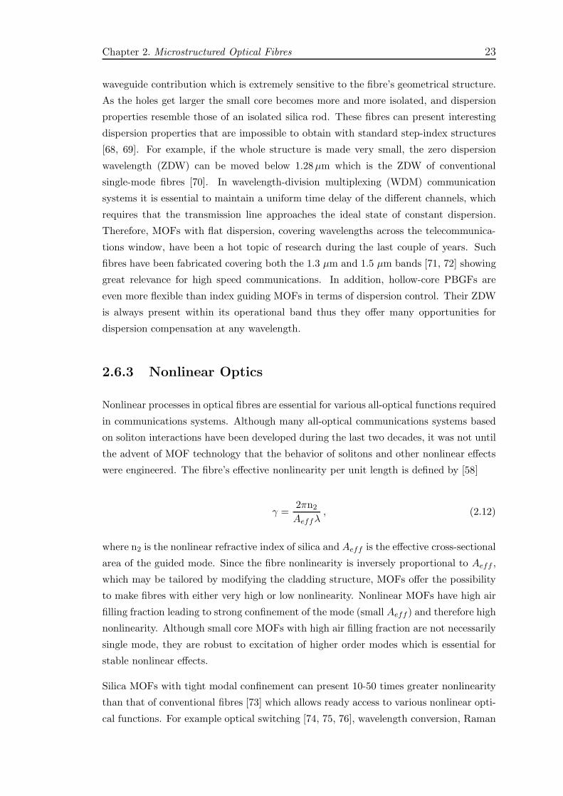
Chapter 2. Microstructured Optical Fibres 23
waveguide contribution which is extremely sensitive to the fibre’s geometrical structure.
As the holes get larger the small core becomes more and more isolated, and dispersion
properties resemble those of an isolated silica rod. These fibres can present interesting
dispersion properties that are impossible to obtain with standard step-index structures
[68, 69]. For example, if the whole structure is made very small, the zero dispersion
wavelength (ZDW) can be moved below 1.28µm which is the ZDW of conventional
single-mode fibres [70]. In wavelength-division multiplexing (WDM) communication
systems it is essential to maintain a uniform time delay of the different channels, which
requires that the transmission line approaches the ideal state of constant dispersion.
Therefore, MOFs with flat dispersion, covering wavelengths across the telecommunica-
tions window, have been a hot topic of research during the last couple of years. Such
fibres have been fabricated covering both the 1.3 µm and 1.5 µm bands [71, 72] showing
great relevance for high speed communications. In addition, hollow-core PBGFs are
even more flexible than index guiding MOFs in terms of dispersion control. Their ZDW
is always present within its operational band thus they offer many opportunities for
dispersion compensation at any wavelength.
2.6.3 Nonlinear Optics
Nonlinear processes in optical fibres are essential for various all-optical functions required
in communications systems. Although many all-optical communications systems based
on soliton interactions have been developed during the last two decades, it was not until
the advent of MOF technology that the behavior of solitons and other nonlinear effects
were engineered. The fibre’s effective nonlinearity per unit length is defined by [58]
γ =2πn2
Aeffλ, (2.12)
where n2 is the nonlinear refractive index of silica and Aeff is the effective cross-sectional
area of the guided mode. Since the fibre nonlinearity is inversely proportional to Aeff ,
which may be tailored by modifying the cladding structure, MOFs offer the possibility
to make fibres with either very high or low nonlinearity. Nonlinear MOFs have high air
filling fraction leading to strong confinement of the mode (small Aeff ) and therefore high
nonlinearity. Although small core MOFs with high air filling fraction are not necessarily
single mode, they are robust to excitation of higher order modes which is essential for
stable nonlinear effects.
Silica MOFs with tight modal confinement can present 10-50 times greater nonlinearity
than that of conventional fibres [73] which allows ready access to various nonlinear opti-
cal functions. For example optical switching [74, 75, 76], wavelength conversion, Raman

Chapter 2. Microstructured Optical Fibres 24
amplification [77], parametric processes [78], soliton generation squeezing [79, 80], and
supercontinuum generation [81, 82, 83, 84, 85] have been explored with MOFs. When
high-energy short pulses (picosecond or femtosecond) travel through a material, their fre-
quency spectrum can be broadened by the combination of various nonlinear effects [86].
The possibility of tailoring the dispersion characteristics of small core MOFs combined
with their high nonlinearity has led to perhaps one of the most exciting applications of
MOFs, supercontinuum generation spanning from 400nm to 2000 nm. The first demon-
stration of a supercontinuum in a PCF used a fibre whose core was small enough to
give zero dispersion at 800 nm, which is near the emission wavelength of a Ti:sapphire
femtosecond pump laser [81]. Supercontinuum lasers find applications in medicine [87],
metrology, spectroscopy, and many other areas [86]. Figure 2.7 shows a supercontinuum
fibre laser that is used to study photon/plasmon interactions in metal-filled MOFs in
Chapter 7.
Figure 2.7: Supercontinuum laser generation using a high nonlinear MOF.Nanosecond infrared pulses are coupled into the fibre core where visible lightis generated due to nonlinear processes. The photograph shows the nonlinearfibre and a prism used as a diffraction medium. This laser has been used for
plasmon experiments in Chapter 7.
In order to further increase the effective nonlinearity per unit length, fibres made of high
index and high nonlinearity glasses have been fabricated [88, 89]. Using our technology
the deposition of material with even higher nonlinearity than glasses, such as semicon-
ductors, into the holes of MOFs is possible and may offer new opportunities in nonlinear
optics. For example, it is difficult to generate laser light at wavelengths beyond those
offered by the small window of available lasers. The efficient transfer of laser energy to
new wavelengths, by stimulated Raman conversion, is therefore a very attractive way of
generating light.
Chapter 2. Microstructured Optical Fibres 25
Spontaneous Raman scattering is caused by molecular vibrations, that interact sponta-
neously with the incident light, shifting its frequency both up (anti-Stokes) and down
(Stokes). The Stokes signal is stronger than the anti-Stokes, due to Boltzmann distri-
bution of occupying molecular states, and at high laser intensities is the predominant
molecular oscillation. Ultimately, above a certain threshold power, the process becomes
stimulated and the major fraction of the pump power is converted to the Stokes fre-
quency. Semiconductors such as silicon and germanium have much larger Raman coeffi-
cients than silica which make them a good prospect for Raman wavelength conversion.
A fibre which guides light in a silicon or germanium core, may be useful to generate
Stokes wavelengths in very short fibre lengths and with low threshold. Moreover, be-
cause these semiconductors are transparent in the infrared, outside silica’s transmission
window, they have excellent prospects for MID-IR light generation.
2.7 Modelling Microstructured Optical Fibres
Having reviewed the fabrication, properties and applications of existing MOFs and the
exciting possibilities offered by material deposition within their capillaries, it is necessary
to understand the optical properties of these material-modified MOFs. This section
provides a short discussion of the most extensively used numerical methods for analysing
MOF. As mentioned, when complex fibre geometries are to be analyzed, the solution of
equation 2.5 in a close form is not usually possible and powerful computational tools are
required. This is the case when the goal is to provide a solution to the optical modes in
microstructured optical fibres. Various parameters including the size, pitch, shape of the
holes, number of holes, etc. affect the properties of MOFs. As it has been shown in the
previous sections, the proper choice of these parameters permits the design of particular
fibres for an intended application. Furthermore, due to the relatively high-refractive
index difference of MOFs, it is necessary to apply full-vector methods and prevents us
from employing scalar approximations that lead, for example, to the definition of LP
modes of step-index fibres.
In recent years a significant amount of work has been devoted to the formulation of
full-vector numerical methods for the modelling of MOFs. Methods such as Beam Prop-
agation, Plane Wave Expansion, localized function, multipole method, Finite-Difference
Time and Frequency domains, as well as Finite Element Method have been adapted/de-
veloped for the accurate description of both index-guiding and photonic bandgap fibres.
It is worth briefly describing some of these methods because the deposition of submicron
layers of semiconductor and/or metals within the fibre holes makes the computational
task even more complicated, and a good understanding of the possibilities of each method
Chapter 2. Microstructured Optical Fibres 26
has been useful to predict the behavior of material modified fibres. The next section
provides an overview of the main methods that have been applied for the solution of the
eigenproblem (equation (2.5)) in MOFs.
2.7.1 Full-vector Plane-wave Expansion Method (FVPWE)
This was the first theoretical approach proposed to find the photonic bandgaps of pho-
tonic crystals. FVPWE is based on the methods used to obtain electronic bandgaps in
semiconductor crystals. It is particularly well-suited to calculate the bandgap of peri-
odic structures, and the modes allowed within the photonic bandgap by defects. For
a full periodic structure, according to the Bloch theorem, the solution to the vectorial
wave equation may be expressed as a plane wave modulated by a periodic function with
the same periodicity as the photonic crystal (equation (2.8)). As the solutions to the
problem are periodic, it is convenient to operate in the reciprocal space. Thus, the solu-
tions and the periodic dielectric constant distribution are expressed as a Fourier-series
expansion in terms of the reciprocal lattice vectors [4]. FVPWE has been one of the
major tools for the analysis of MOFs with periodic dielectric perturbations [90].
2.7.2 Orthogonal Basis Functions Techniques
Orthogonal basis techniques are based on the direct solution of Maxwell equations, using
a representation of the refractive index and the field distributions as a sum of orthogonal
functions. Because guided modes of PCFs are localized in the core vicinity, it is possible
to calculate them by representing the electromagnetic field as sums of localized functions
in the core vicinity. The expansion coefficients are obtained by overlapping integrals
between the localized basis functions and the fibre refractive index distribution. Using
this, Maxwell’s equations are reformulated as an eigenvalue problem for the propagation
constant of the modes. The first scalar localized functions method was developed by
Mogilevtsev et al., using a Hermite-Gaussian basis [70]. Since then, the orthogonal basis
functions technique has been extended and further developed by other scientists. For
example, in the work by Monro and co-workers the transverse refractive index profile
is represented with two orthogonal basis functions [62]. The periodic lattice of holes
is described using periodic functions (e.g. as a Fourier series) and the central defect is
described using Hermite-Gaussian functions. Because of the reduced number of terms
needed to accurately represent the refractive index profile, this method allows for a fast
and efficient computation. Although orthogonal basis function techniques were very
useful to obtain a good description of the optical properties of MOFs during their early
years, they are not very flexible in terms of calculating aperiodic fibre structures [24].

Chapter 2. Microstructured Optical Fibres 27
2.7.3 Beam Propagation Method
The beam propagation method (BPM) is a well-established tool of analysis for field
distribution in integrated photonic devices. BPM uses numerical algorithms to simulate
the propagation of a coherent beam along any arbitrary structure and obtain its field
distribution [91, 92, 93, 94]. In BPM an initial field distribution propagates step by step
in the longitudinally direction of the photonic structure. Although a paraxial approxi-
mation is usually employed in order to reduce the computational time, BPM can easily
be extended to wide-angle problems. It is also possible to take into account the vectorial
nature of the electromagnetic wave making it suitable for the analysis of MOFs. BPM
it is not designed to calculate the optical modes of a structure; however there are some
expansions of BPM which make it possible to provide mode-solving capability. For ex-
ample, imaginary-distance BPM [95] the fundamental mode is obtained by propagating
an initial mode profile along an imaginary distance direction (iz). Then the oscillating
term eiβz becomes a gain term eiβz. As the fundamental mode is characterised by the
largest propagation constant, its intensity will increase at the higher growth rate and its
profile will dominate all other modes after a short distance, higher order modes can be
sequentially obtained. This method is suitable for the modeling of semiconductor and
polymer optical fibres many optical properties of filled MOFs such as, mode structure
and optical loss.
Finally, it is worth noting that many numerical methods have been used to efficiently pre-
dict the optical properties of photonic crystals, and in particular, the multipole method
and finite element method (FEM) are of great interest for this research.
2.8 Semiconductor Photonic Bandgap Fibres
The spectral position and extent of bandgaps are highly dependent on the optical proper-
ties of the material which form a photonic crystal. Therefore, the inclusion of materials,
whose optical properties can be easily modified, within the capillary voids of PBGF
offer opportunities to developing tuneable photonic devices such as filters, modulators
and variable attenuators based on bandgap effects. Bise and colleagues demonstrated a
solid silica core tuneable PBGF [96]. For this experiment the cladding holes were filled
with high refractive index oil and, by thermally modifying its refractive index, they
were able to tune the band gap structure of the fibre, and therefore its transmission
properties. Subsequently, tuneable photonic bandgap fibres based on the thermo-optic
response of liquid crystals (LCs) were demonstrated [34]. In this work, Larsen et al.
filled LCs into the circular voids of a triangular structured MOFs. The relatively high,
and controllable refractive index of the LC, together with the periodic arrangement of
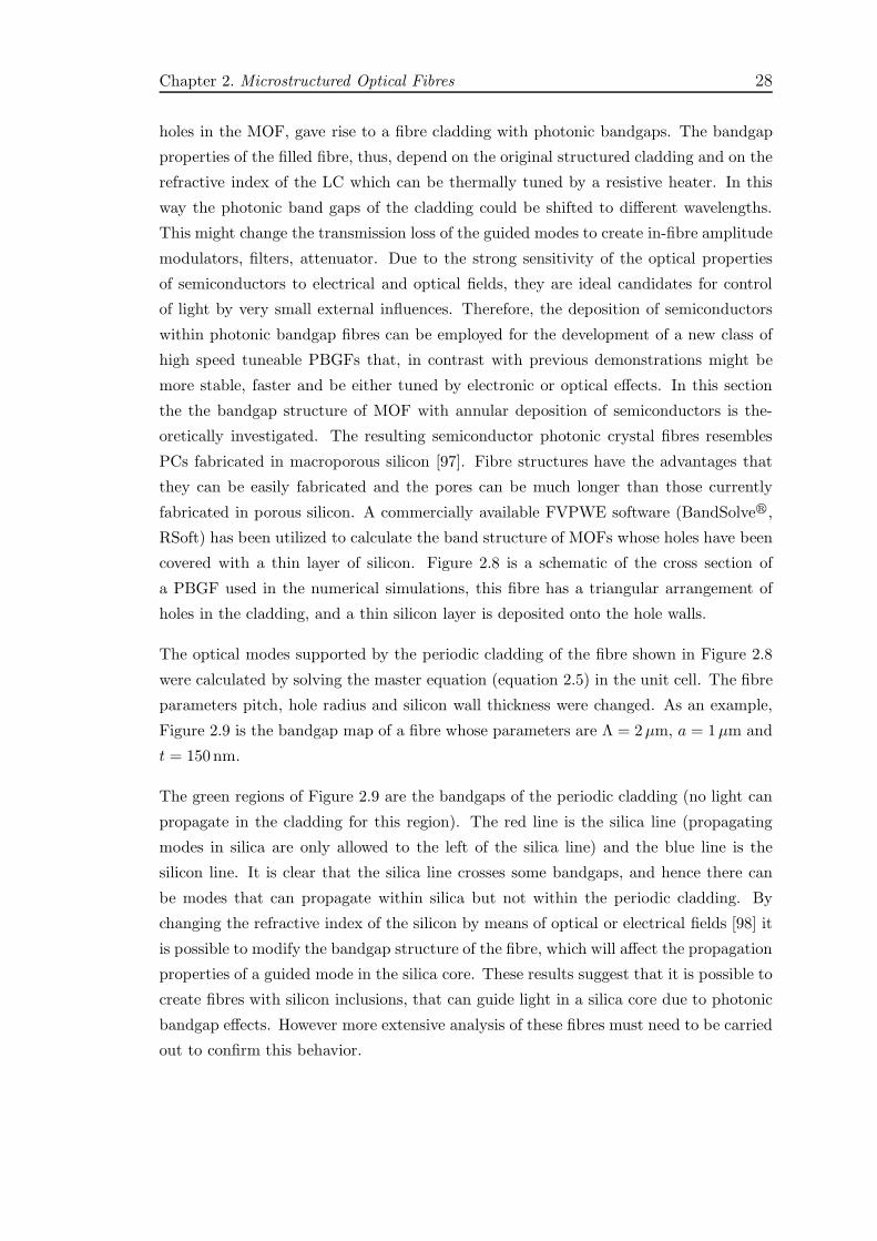
Chapter 2. Microstructured Optical Fibres 28
holes in the MOF, gave rise to a fibre cladding with photonic bandgaps. The bandgap
properties of the filled fibre, thus, depend on the original structured cladding and on the
refractive index of the LC which can be thermally tuned by a resistive heater. In this
way the photonic band gaps of the cladding could be shifted to different wavelengths.
This might change the transmission loss of the guided modes to create in-fibre amplitude
modulators, filters, attenuator. Due to the strong sensitivity of the optical properties
of semiconductors to electrical and optical fields, they are ideal candidates for control
of light by very small external influences. Therefore, the deposition of semiconductors
within photonic bandgap fibres can be employed for the development of a new class of
high speed tuneable PBGFs that, in contrast with previous demonstrations might be
more stable, faster and be either tuned by electronic or optical effects. In this section
the the bandgap structure of MOF with annular deposition of semiconductors is the-
oretically investigated. The resulting semiconductor photonic crystal fibres resembles
PCs fabricated in macroporous silicon [97]. Fibre structures have the advantages that
they can be easily fabricated and the pores can be much longer than those currently
fabricated in porous silicon. A commercially available FVPWE software (BandSolver,
RSoft) has been utilized to calculate the band structure of MOFs whose holes have been
covered with a thin layer of silicon. Figure 2.8 is a schematic of the cross section of
a PBGF used in the numerical simulations, this fibre has a triangular arrangement of
holes in the cladding, and a thin silicon layer is deposited onto the hole walls.
The optical modes supported by the periodic cladding of the fibre shown in Figure 2.8
were calculated by solving the master equation (equation 2.5) in the unit cell. The fibre
parameters pitch, hole radius and silicon wall thickness were changed. As an example,
Figure 2.9 is the bandgap map of a fibre whose parameters are Λ = 2µm, a = 1µm and
t = 150nm.
The green regions of Figure 2.9 are the bandgaps of the periodic cladding (no light can
propagate in the cladding for this region). The red line is the silica line (propagating
modes in silica are only allowed to the left of the silica line) and the blue line is the
silicon line. It is clear that the silica line crosses some bandgaps, and hence there can
be modes that can propagate within silica but not within the periodic cladding. By
changing the refractive index of the silicon by means of optical or electrical fields [98] it
is possible to modify the bandgap structure of the fibre, which will affect the propagation
properties of a guided mode in the silica core. These results suggest that it is possible to
create fibres with silicon inclusions, that can guide light in a silica core due to photonic
bandgap effects. However more extensive analysis of these fibres must need to be carried
out to confirm this behavior.
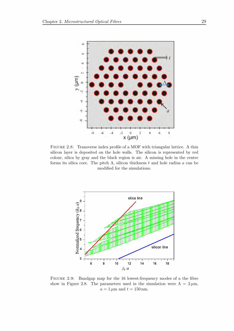
Chapter 2. Microstructured Optical Fibres 29
Figure 2.8: Transverse index profile of a MOF with triangular lattice. A thinsilicon layer is deposited on the hole walls. The silicon is represented by redcolour, silica by gray and the black region is air. A missing hole in the centreforms its silica core. The pitch Λ, silicon thickness t and hole radius a can be
modified for the simulations.
Figure 2.9: Bandgap map for the 16 lowest-frequency modes of a the fibreshow in Figure 2.8. The parameters used in the simulation were Λ = 2µm,
a = 1µm and t = 150nm.

Chapter 3
Materials Deposition inside
Microstructured Optical Fibres
The fibres studied in this thesis are fabricated in what can be considered to be a two
step process: first silica/air MOFs are made using the stacking and drawing method.
Afterwards, in an independent process, materials are deposited inside MOFs capillaries,
to give maximum design flexibility over both structural and compositional parameter
space. The deposition within MOFs presents considerable challenges to achieve suffi-
cient mass transport of the precursors within the high aspect ratio fibre channels, due to
the fact that the flow is restricted by the small capillary dimensions and the deposited
material itself. Thus the use of traditional deposition methods, such as those used for in-
tegrated circuit (IC) fabrication, are limited by the fibre structure and more appropriate
techniques are required.
This chapter gives an insight into the conventional material processing methods used for
the deposition of semiconductors and metals onto planar substrates and into nanostruc-
tures. The advantages of these deposition methods are discussed and their applicability
within MOFs is analyzed. Finally, this chapter describes the high-pressure chemical
deposition methods that our research team has developed and implemented for the de-
position of crystalline semiconductors, metals and polymers inside the long air channels
of silica MOFs.
The silica MOFs used in this work were fabricated in the ORC and the deposition process
has been carried out in collaboration with Penn State University, in the case of semi-
conductors and with the University of Nottingham for PMMA and silver impregnated
fibres.
30

Chapter 3. Materials Deposition inside Microstructured Optical Fibres 31
3.1 Micro/Nanomaterials Synthesis
What is the smallest possible device with optical, electronic, or magnetic functionality?
Questions like this and the demands of present and future microelectronic, photonic, data
storage and lab-in-a-chip systems for genomics, combined with ideas from great vision-
aries such as Richard Feynman -who predicted the possibility of tailoring the properties
of matter in the sub-micronscale- [99] are fueling interest in the field of nanotechnol-
ogy. At the present time the word nanotechnology is becoming more and more familiar
to scientific and engineering communities because of the numerous opportunities that
this field might open, including building circuits for a new kinds of computers, super-
capacitors, ultra-sensitive molecular sensors, and fabricating the perfect molecular-scale
machines and information systems of living organisms. However, nanotechnology, as all
other technologies, is strongly dependent on its platform materials. Therefore, before
having devices such as those proposed by Feynman more that 40 years ago, stringent
requirements on nanomaterials and nanostructure fabrication methods must be satisfied.
Figure 3.1 is a cartoon of the two main approaches for micro/nanomaterial fabrication:
top-down and bottom-up. Top-down, which is commonly used to produce microchips,
makes use of photolithography, etching and deposition from the vapour phase to carve
out material and create tiny features on substrates. Although this technology allows
complex structures to be made in well-defined positions, it requires substantial effort
when extended to scales below 100 nm. It is intrinsically planar and its extension to 3D
is limited to the stacking of planar structures.
Figure 3.1: Cartoon of top-down and bottom-up nanofabrication techniques.From reference [100].
The second nanomaterial fabrication method is known as templating or bottom-up. It
entails synthesizing the desired material within the holes of a preordered template. The
material deposited within the holes will follow the structure of the template. Because
the template and the deposited material are formed in discrete processes, many different
materials can be deposited inside the structure. Porous templates can be made of
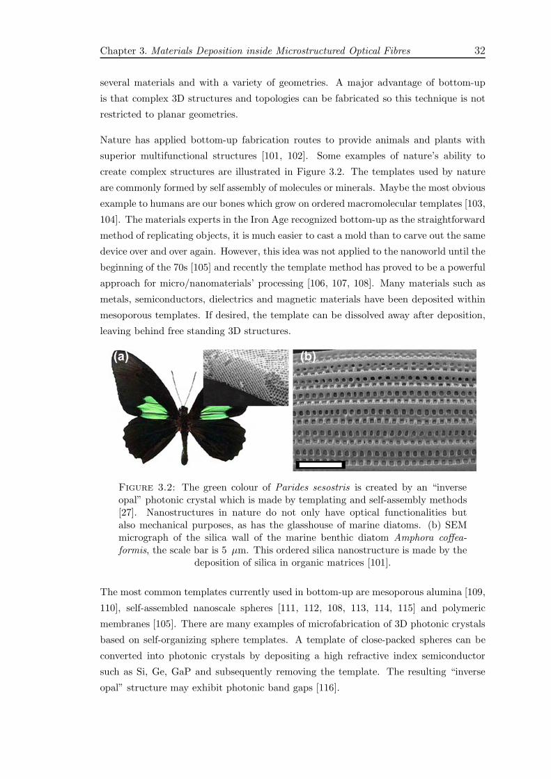
Chapter 3. Materials Deposition inside Microstructured Optical Fibres 32
several materials and with a variety of geometries. A major advantage of bottom-up
is that complex 3D structures and topologies can be fabricated so this technique is not
restricted to planar geometries.
Nature has applied bottom-up fabrication routes to provide animals and plants with
superior multifunctional structures [101, 102]. Some examples of nature’s ability to
create complex structures are illustrated in Figure 3.2. The templates used by nature
are commonly formed by self assembly of molecules or minerals. Maybe the most obvious
example to humans are our bones which grow on ordered macromolecular templates [103,
104]. The materials experts in the Iron Age recognized bottom-up as the straightforward
method of replicating objects, it is much easier to cast a mold than to carve out the same
device over and over again. However, this idea was not applied to the nanoworld until the
beginning of the 70s [105] and recently the template method has proved to be a powerful
approach for micro/nanomaterials’ processing [106, 107, 108]. Many materials such as
metals, semiconductors, dielectrics and magnetic materials have been deposited within
mesoporous templates. If desired, the template can be dissolved away after deposition,
leaving behind free standing 3D structures.
Figure 3.2: The green colour of Parides sesostris is created by an “inverseopal” photonic crystal which is made by templating and self-assembly methods[27]. Nanostructures in nature do not only have optical functionalities butalso mechanical purposes, as has the glasshouse of marine diatoms. (b) SEMmicrograph of the silica wall of the marine benthic diatom Amphora coffea-
formis, the scale bar is 5 µm. This ordered silica nanostructure is made by thedeposition of silica in organic matrices [101].
The most common templates currently used in bottom-up are mesoporous alumina [109,
110], self-assembled nanoscale spheres [111, 112, 108, 113, 114, 115] and polymeric
membranes [105]. There are many examples of microfabrication of 3D photonic crystals
based on self-organizing sphere templates. A template of close-packed spheres can be
converted into photonic crystals by depositing a high refractive index semiconductor
such as Si, Ge, GaP and subsequently removing the template. The resulting “inverse
opal” structure may exhibit photonic band gaps [116].
Chapter 3. Materials Deposition inside Microstructured Optical Fibres 33
The range of template structures that can be formed, and their extent and perfec-
tion restricts the possibilities of bottom-up [117] fabrication. Therefore, the search for
new templates with highly controlled geometry is essential for bottom-up and micro/-
nanosciences. The merit of a particular template structure, if it is to find wide practical
application, will be defined by its robustness, temporal and mechanical stability, and its
ability to be easily integrated within existing technological infrastructures. With these
criteria in mind, one can conclude that MOFs present a number of attractive properties,
such as very large internal surface areas, high aspect ratios and outstanding mechanical
properties, making them excellent lithography free, robust and inexpensive 3D templates
for materials deposition.
A limitation of using MOFs as templates is that the material deposition methods cur-
rently applied in microelectronics and nanofabrication do not allow conformal coverage
and/or complete filling of MOFs narrow high aspect capillary holes. Therefore, our
research group has explored new high pressure deposition methods for achieving this
task.
3.2 Vapour Phase Deposition
Material deposition methods fall into two broad categories: vapour and liquid phase
techniques depending on the physical state of the carrying medium which is used to
transport the precursor to the substrate.
This section describes the main characteristics of vapour phase deposition (VPD) which
is the process whereby gas phase species are condensed, chemically reacted or converted
into solid deposits. Vapour deposition techniques are divided into two main categories:
physical vapour deposition and chemical vapour deposition. Due to the absence of
surface tension in gases, they can completely wet complex topologies. Therefore, vapour
precursors provide a powerful medium for the conformal deposition within mesoporous
substrates [118]. During the last decades the deposition of high quality thin films, free
standing structures and mesoporous materials by vapour deposition methods have been
demonstrated. As will be described in the following sections, our research group has
developed high-pressure vapour phase techniques for growing amorphous and crystalline
silicon and germanium wire/tubes within MOFs [16].
3.2.1 Physical Vapour Deposition
Physical Vapour Deposition (PVD)is typically a direct line-of-sight technique in which
the gaseous precursor is produced by either evaporating or ablating the target material.

Chapter 3. Materials Deposition inside Microstructured Optical Fibres 34
The evaporated atoms or molecules solidify onto a substrate and form films. In order to
obtain high quality deposits and to allow the particles to travel as freely as possible, the
whole process takes place in a vacuum chamber. Many PVD techniques can produce high
purity films and have found increased use in the microelectronics and optoelectronics
industries, especially for the fabrication of film resistors and filters. The most common
PVD methods are: thermal vapour deposition, sputtering, laser ablation deposition and
molecular beam epitaxy (MBE) which is particulary useful for top-down micro/nano
fabrication, where device quality is at a premium.
3.2.1.1 Thermal Vapour Deposition (TVD)
Thermal evaporation represents one of the oldest of the thin film deposition techniques
and, at present, many different kinds of films in integrated circuits are deposited by evap-
oration. The material to be deposited is heated to its melting temperature in a vacuum,
which allows its vapour to reach the substrate surface and grow thin films [119]. The
material is usually evaporated by passing current through a high melting temperature
metal (e.g., a tungsten boat or filament). In industrial applications, resistive heating has
been replaced by electron beam and RF induction evaporation [118]. TVD is suitable
for film growth of materials with simple stoichiometry, making it very common for metal
deposition. Indeed, a wide range of metals and alloy thin films such as Au, Al, Ag, Ni,
Ni-Cr [120], Ti-Al-V, Ni-Cr-Al [121] have been effectively deposited. This technique is
not suitable for compound materials or materials with complex stoichiometries because
the different vapour pressures of their constituents would lead to deposits with incor-
rect compositions. TVD offers almost no control over the path taken by the evaporated
atoms, with consequent slow growth rates, and inefficient use of the source material.
Some variations of TVD, such as MBE, offer great control of the deposition process
even down to the level of atomic monolayer precision. However, because the process
has to take place in a vacuum chamber, the vapour cannot wet the internal walls of
mesoporous templates. A representation of a TVD chamber is illustrated in Figure 3.3.
3.2.1.2 Sputtering
A schematic of a sputtering chamber is shown in Figure 3.4. During the deposition pro-
cess, the solid coating material (target), at a high negative potential, is converted into
vapour phase by ion bombardment (Ar+). The vaporized material is condensed onto the
substrate placed on the anode [119]. Although sputtering coating always takes place in
the presence of plasma, the pressure in the vacuum chamber is always kept very low and
the evaporated atoms follow a more or less collision-less path to the substrate. Sputter-
ing is preferred over evaporation in many applications due to the fact that virtually any

Chapter 3. Materials Deposition inside Microstructured Optical Fibres 35
Figure 3.3: Illustration of a typical TVD deposition chamber. Only materialswith a much higher vapor pressure than the heating element can be depositedwithout contamination of the film. TVD requires good vacuum during evapo-
ration, and pressures lower than 10−6 Pa are normally used.
material can be sputtered and has better adhesion to the substrate. This technique is
commonly used for the deposition of metals, semiconductors and dielectrics onto inte-
grated circuit wafers. An important advantage of the sputtering process is its capacity to
convert the material into gas phase without changing its chemical composition, resulting
in high purity deposits.
PVD methods have many features which have permitted them to be widely used at
laboratory and industrial levels. In PVD, the starting materials are chemically pure and
the deposition takes place in a vacuum chamber, thus these methods usually have fewer
contamination problems than other deposition techniques. However, since the evapo-
rated particles tend to follow a straight path (line-of-sight), films deposited by physical
means are commonly directional rather than conformal which prohibits them from form-
ing homogeneous films within mesoporous structures. Moreover, since PVD are vacuum
deposition processes, there is limited mass transport down the extreme aspect-ratio cap-
illaries of MOFs. Thus, PVD techniques cannot be applied to our purposes and chemical
methods are must be considered.
3.2.2 Chemical Vapour Deposition
Chemical Vapour Deposition (CVD) is a non-line-of-sight deposition process whereby
chemical reactions produce solid material from gaseous reagents on or near the surface
of a heated substrate. The constituents in the vapour phase are typically diluted with an
inert carrier gas and react at the surface of hot substrates [122]. CVD has developed into
one of the most versatile and important methods for material synthesis and today has
application to a wide spectrum of compounds. CVD plays a central role in the synthesis
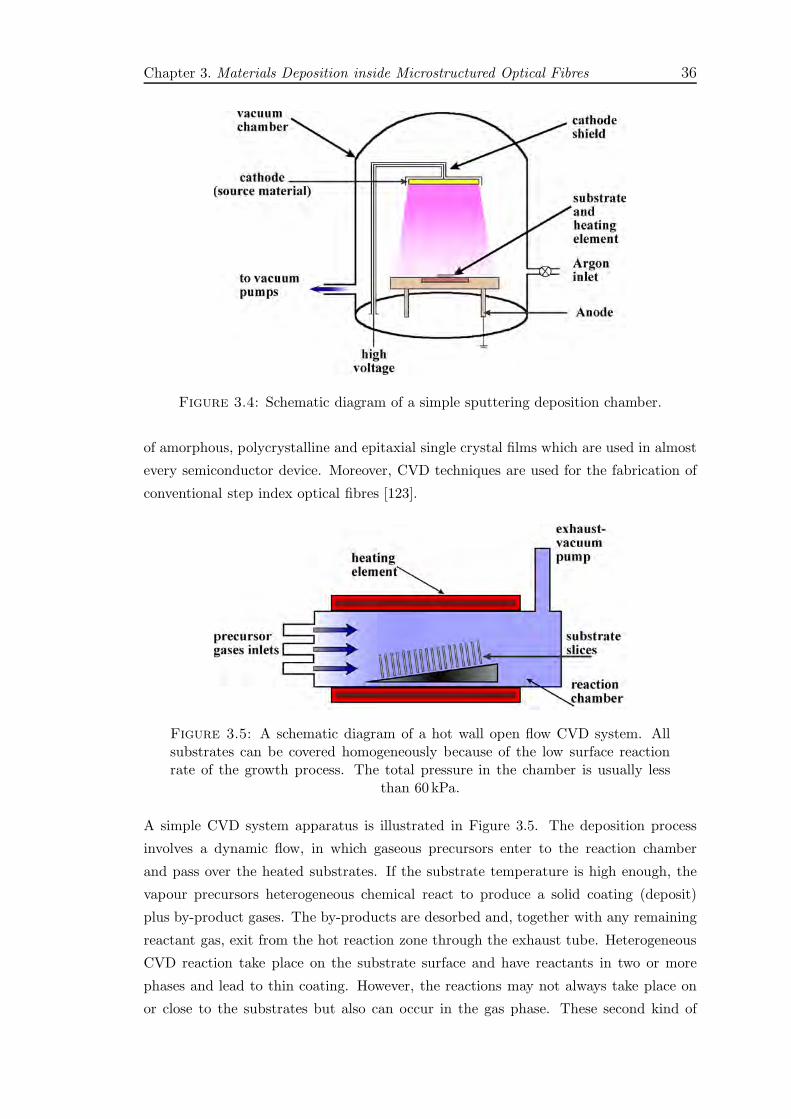
Chapter 3. Materials Deposition inside Microstructured Optical Fibres 36
Figure 3.4: Schematic diagram of a simple sputtering deposition chamber.
of amorphous, polycrystalline and epitaxial single crystal films which are used in almost
every semiconductor device. Moreover, CVD techniques are used for the fabrication of
conventional step index optical fibres [123].
Figure 3.5: A schematic diagram of a hot wall open flow CVD system. Allsubstrates can be covered homogeneously because of the low surface reactionrate of the growth process. The total pressure in the chamber is usually less
than 60 kPa.
A simple CVD system apparatus is illustrated in Figure 3.5. The deposition process
involves a dynamic flow, in which gaseous precursors enter to the reaction chamber
and pass over the heated substrates. If the substrate temperature is high enough, the
vapour precursors heterogeneous chemical react to produce a solid coating (deposit)
plus by-product gases. The by-products are desorbed and, together with any remaining
reactant gas, exit from the hot reaction zone through the exhaust tube. Heterogeneous
CVD reaction take place on the substrate surface and have reactants in two or more
phases and lead to thin coating. However, the reactions may not always take place on
or close to the substrates but also can occur in the gas phase. These second kind of
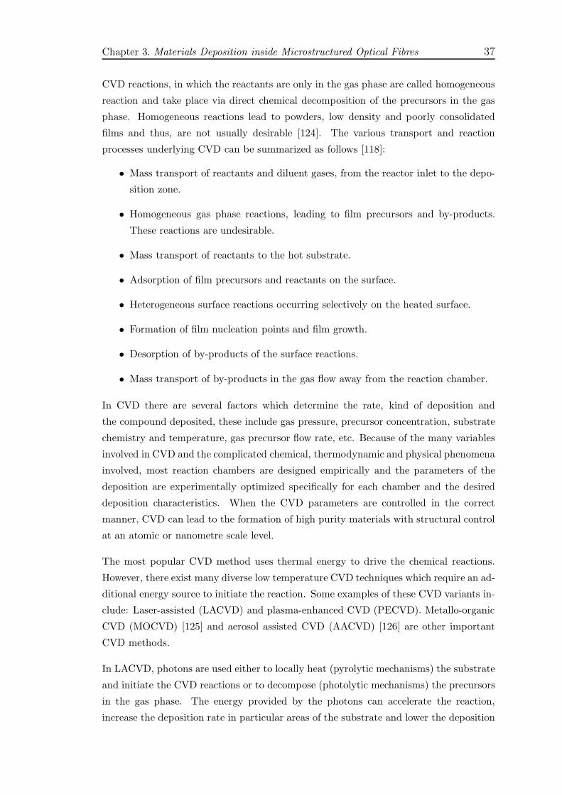
Chapter 3. Materials Deposition inside Microstructured Optical Fibres 37
CVD reactions, in which the reactants are only in the gas phase are called homogeneous
reaction and take place via direct chemical decomposition of the precursors in the gas
phase. Homogeneous reactions lead to powders, low density and poorly consolidated
films and thus, are not usually desirable [124]. The various transport and reaction
processes underlying CVD can be summarized as follows [118]:
• Mass transport of reactants and diluent gases, from the reactor inlet to the depo-
sition zone.
• Homogeneous gas phase reactions, leading to film precursors and by-products.
These reactions are undesirable.
• Mass transport of reactants to the hot substrate.
• Adsorption of film precursors and reactants on the surface.
• Heterogeneous surface reactions occurring selectively on the heated surface.
• Formation of film nucleation points and film growth.
• Desorption of by-products of the surface reactions.
• Mass transport of by-products in the gas flow away from the reaction chamber.
In CVD there are several factors which determine the rate, kind of deposition and
the compound deposited, these include gas pressure, precursor concentration, substrate
chemistry and temperature, gas precursor flow rate, etc. Because of the many variables
involved in CVD and the complicated chemical, thermodynamic and physical phenomena
involved, most reaction chambers are designed empirically and the parameters of the
deposition are experimentally optimized specifically for each chamber and the desired
deposition characteristics. When the CVD parameters are controlled in the correct
manner, CVD can lead to the formation of high purity materials with structural control
at an atomic or nanometre scale level.
The most popular CVD method uses thermal energy to drive the chemical reactions.
However, there exist many diverse low temperature CVD techniques which require an ad-
ditional energy source to initiate the reaction. Some examples of these CVD variants in-
clude: Laser-assisted (LACVD) and plasma-enhanced CVD (PECVD). Metallo-organic
CVD (MOCVD) [125] and aerosol assisted CVD (AACVD) [126] are other important
CVD methods.
In LACVD, photons are used either to locally heat (pyrolytic mechanisms) the substrate
and initiate the CVD reactions or to decompose (photolytic mechanisms) the precursors
in the gas phase. The energy provided by the photons can accelerate the reaction,
increase the deposition rate in particular areas of the substrate and lower the deposition
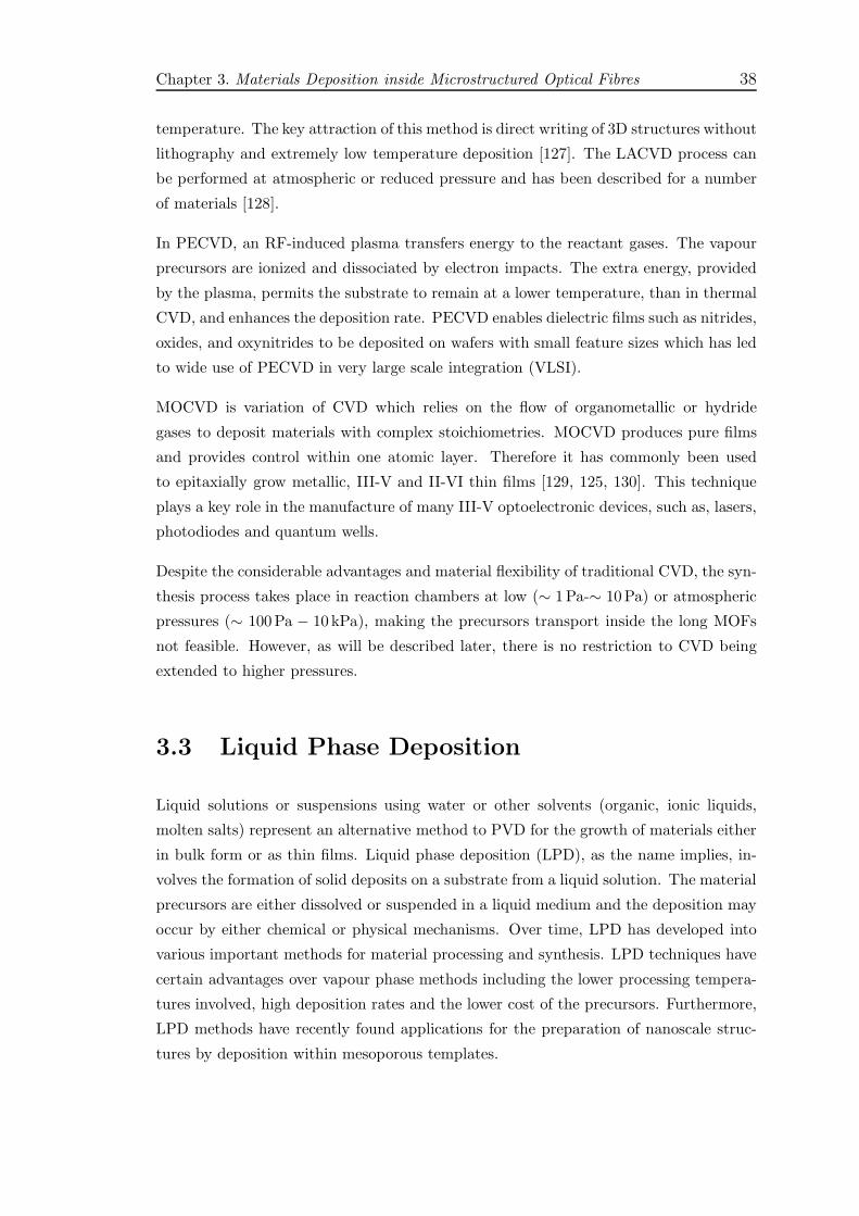
Chapter 3. Materials Deposition inside Microstructured Optical Fibres 38
temperature. The key attraction of this method is direct writing of 3D structures without
lithography and extremely low temperature deposition [127]. The LACVD process can
be performed at atmospheric or reduced pressure and has been described for a number
of materials [128].
In PECVD, an RF-induced plasma transfers energy to the reactant gases. The vapour
precursors are ionized and dissociated by electron impacts. The extra energy, provided
by the plasma, permits the substrate to remain at a lower temperature, than in thermal
CVD, and enhances the deposition rate. PECVD enables dielectric films such as nitrides,
oxides, and oxynitrides to be deposited on wafers with small feature sizes which has led
to wide use of PECVD in very large scale integration (VLSI).
MOCVD is variation of CVD which relies on the flow of organometallic or hydride
gases to deposit materials with complex stoichiometries. MOCVD produces pure films
and provides control within one atomic layer. Therefore it has commonly been used
to epitaxially grow metallic, III-V and II-VI thin films [129, 125, 130]. This technique
plays a key role in the manufacture of many III-V optoelectronic devices, such as, lasers,
photodiodes and quantum wells.
Despite the considerable advantages and material flexibility of traditional CVD, the syn-
thesis process takes place in reaction chambers at low (∼ 1Pa-∼ 10Pa) or atmospheric
pressures (∼ 100Pa − 10 kPa), making the precursors transport inside the long MOFs
not feasible. However, as will be described later, there is no restriction to CVD being
extended to higher pressures.
3.3 Liquid Phase Deposition
Liquid solutions or suspensions using water or other solvents (organic, ionic liquids,
molten salts) represent an alternative method to PVD for the growth of materials either
in bulk form or as thin films. Liquid phase deposition (LPD), as the name implies, in-
volves the formation of solid deposits on a substrate from a liquid solution. The material
precursors are either dissolved or suspended in a liquid medium and the deposition may
occur by either chemical or physical mechanisms. Over time, LPD has developed into
various important methods for material processing and synthesis. LPD techniques have
certain advantages over vapour phase methods including the lower processing tempera-
tures involved, high deposition rates and the lower cost of the precursors. Furthermore,
LPD methods have recently found applications for the preparation of nanoscale struc-
tures by deposition within mesoporous templates.

Chapter 3. Materials Deposition inside Microstructured Optical Fibres 39
3.3.1 Electrochemical Deposition
Electrochemical deposition refers to the growth of a material or alloys from a conductive
solution (electrolyte) containing ions of the material to be deposited. The deposition
occurs on the cathode’s surface, by the flow of an electric current between two elec-
trodes immersed in the solution. Many metals have been deposited within the holes
of porous alumina, polycarbonate and polymer templates by the electrochemical reduc-
tion of metals ions [131, 132, 133]. Figure 3.6 shows examples of gold wires formed by
electrodeposition within alumina templates. The membrane employed has cylindrical
pore geometry, with monodisperse diameters that extend through the entire thickness
of the membrane. The deposition is done by simply coating one end of the template
with a metal layer and using this film as a cathode. The deposition is initiated on the
cathode and the material grows following the geometry of the pores. It usually results
in well-defined, high aspect ratio, nanowires or nanotubes. If desired, after the deposi-
tion the template can be dissolved away leaving behind the resulting metal structures.
Nanowires and nanotubes of metals like gold, silver, platinum, copper, nickel have been
prepared by electrochemistry. This technique has been prefered for the deposition of
metals however many researchers have applied it for the deposition of semiconductor
films on planar [134] and porous [135, 136] substrates.
Although electrochemistry has shown to be an excellent bottom-up template processing
technique, the deposition conditions required in this method make it difficult to use
for the impregnation of materials within MOFs templates. The main problem is that
electrodeposition needs a conductive layer onto which the materials are grown. Because
of this, materials could only be deposited at one end of a very long fibre but not in the
central part of it. Another limitation of electrochemical deposition is the need for liquid
precursors solutions, which can not easily diffuse inside centimetre long optical fibres
and would thus prohibit the sufficient mass transport of precursors.
3.3.2 Electroless Deposition
Electroless deposition involves catalytic reactions in an aqueous solution which, in con-
trast to electrodeposition, occur without an external electric current. This technique has
been used to fabricate metal nanotubes within nanoporous templates [137, 138, 139].
Figure 3.7 shows a very interesting experiment by Monk and Walt [38], in which mil-
limetre long gold tubes are grown within microscale capillaries of an optical fibre.
The electroless deposition process can be briefly described as follows, a catalyst is first
applied to all surfaces of the porous membrane, which is afterwards immersed into a
solution containing metal ions and a chemical reduction agent (usually hydrogen). The
Chapter 3. Materials Deposition inside Microstructured Optical Fibres 40
Figure 3.6: Synthesis of gold nanowires in porous alumina template by elec-trochemical deposition. Left: TEM image of a microtomed1 section of aluminamembrane. Right: TEM of Au nanotubes that are 70 nm in diameter within
the pores of a membrane, from reference [131].
reduction of the metal solution to solid metal only occurs on the surface (where the cat-
alyst was previously deposited) and metal films are formed on the walls. This technique
has resulted in the preparation of gold nanotubes ensembles whose wall thickness can be
controlled from a few nanometres to some micrometres. Nanotubes with inside diam-
eters of less than 1 nm, made by electroless deposition of gold, have shown interesting
applications for molecular filtering [137].
Figure 3.7: Synthesis of gold micro-tubes in a 5µm silica capillary by electro-less deposition (end and side views). Silica capillaries (A) are modified with amonolayer of bifunctional silane for gold adhesion (B), deposition of a monolayerof colloidal gold (C). Deposition of bulk gold from solution increases the size ofthe gold layer, eventually forming a uniform layer (D). As deposition progresses,the gold thickness approaches the radius of the capillary (E), microscope images
of the resulting gold tubes (F G H). Taken from reference [38]
Both LPD methods, electrochemical and electroless deposition, require the diffusion of
the precursor solutions through the template pores. Thus, these techniques are usually
1A microtome is a mechanical instrument used to cut samples into thin segments for micro-scopic examination, usually 1 to 20 µm thick.

Chapter 3. Materials Deposition inside Microstructured Optical Fibres 41
limited to thin substrates (≃ 100µm), or else deposition must be conducted over long
periods of time (days) or cannot be achieved due to insufficient mass transport of the
precursor far into the capillaries [38]. More than likely, this would be an inherently time
consuming process for high aspect ratio features like MOFs capillaries. Furthermore,the
removal of the liquid precursor solution and reaction by-products from the fibre holes
would be a difficult task after the deposition inside long MOFs.
3.4 Supercritical Fluid Deposition
In order to develop a flexible method for the deposition within mesoporous templates, it
is necessary to think of a technique that combines characteristics of both vapour and liq-
uid phase methods. This method should present the desirable attributes of both vapour
and aqueous techniques while minimizing the disadvantages of each. Evidently, such
a deposition technique would make use of a solvent whose physicochemical properties
resemble those of gases and liquids at the same time!
Fortunately, supercritical fluids (SCF) are gas/liquid hybrids and present exceptional
solvent and transport properties. “Liquid-like” supercritical fluid will dissolve precursors
and will be transported by the “gas-like” supercritical fluid. A fluid is defined to be
supercritical when its temperature and pressure are higher than their critical values,
while it is not far from its critical state. Figure 3.8 depicts the phase diagram of a pure
substance with the critical point labeled (C). When a fluid is in supercritical state, the
difference between coexisting liquid and vapour phases disappears. Liquid and gas join
to form an intermediate state, known as supercritical fluid, that possesses properties of
both.
Figure 3.8: Pressure-temperature phase diagram for a pure substance. Theblue circles illustrate the variation in the substance density. The triple point (T),critical point (C) and the SCF state are all displayed (adapted from reference
[140]).

Chapter 3. Materials Deposition inside Microstructured Optical Fibres 42
The key characteristics of SCFs are the strong temperature and pressure dependence of
their physicochemical properties (density, dielectric constant, viscosity) [141]. By tuning
the temperature or the pressure of a SCF, a state of liquid-like properties can rapidly
transform into one of gas-like properties without the appearance of an interface. These
unusual and intriguing properties can lead to a new branch chemistry including green
chemistry [142] and, in particular, a variety of material processing methods [143].
Supercritical fluid deposition (SCFD) has been extensively used for the deposition of
metals but can also be applied to semiconductors and dielectrics. In the case of metals,
it involves the chemical decomposition of soluble organometallic compounds in a super-
critical fluid such as carbon dioxide (scCO2) to yield high-purity deposits. In the SC
regime, increasing pressure leads only to an increase in fluid density and SCFs’ densities
can approach those of liquids. Since the solubility of fluids directly depends on their
density, various SCFs (including scCO2) are very good solvents. Moreover, the tuning
of the solubility in SCFs can be exploited to control the composition and morphology of
the materials to deposit. Despite near-liquid densities, the transport properties of SCFs
are more akin to those of gases than liquids: in SCFs viscosities are orders of magni-
tude lower and diffusivities orders of magnitude higher than in liquids and SCFs do not
present surface tension (see Table 3.1). Given, the solvating properties near those of
liquids, in combination with viscosities resembling gases, facilitate the dissolution of de-
sired precursor chemicals in a SCF and enables the flow into high aspect ratio channels,
completely wetting the surface. In addition, the low deposition temperature inherent to
solution based techniques, makes SCFD compatible with thermally sensitive substrates
such as polymers.
Figure 3.9: (a) SEM micrograph of SCF deposition of copper films intofeatures as narrow as 45 nm on a silicon wafer, from reference [42]. (b) SEMmicrograph of self-supporting gold arrays deposited by SCFD onto mesoporoussilicon. The micrograph was obtained after removing the substrate, from refer-
ence [144].
SCFs have been shown to be ideal for metal deposition within micro/nano porous sub-
strates including high aspect ratio structures. The use of supercritical fluids to advance
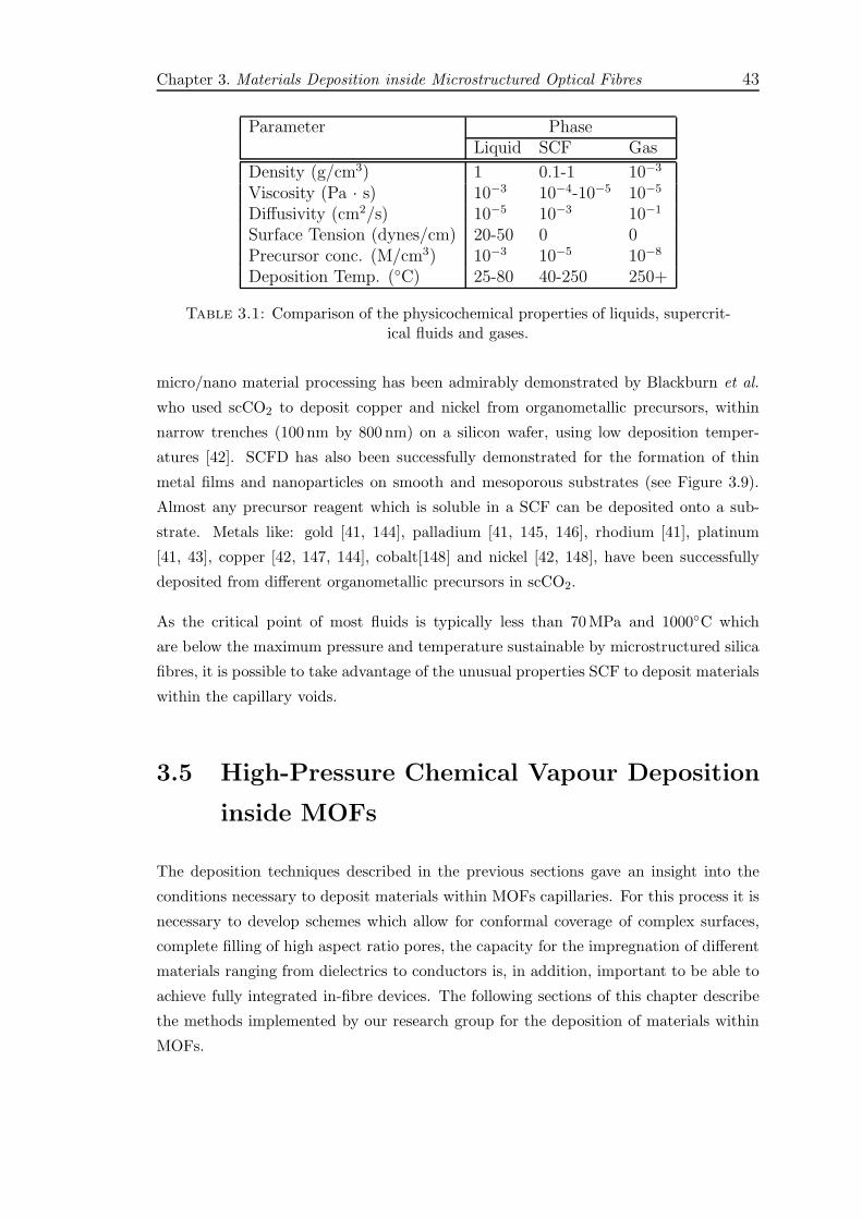
Chapter 3. Materials Deposition inside Microstructured Optical Fibres 43
Parameter PhaseLiquid SCF Gas
Density (g/cm3) 1 0.1-1 10−3
Viscosity (Pa · s) 10−3 10−4-10−5 10−5
Diffusivity (cm2/s) 10−5 10−3 10−1
Surface Tension (dynes/cm) 20-50 0 0Precursor conc. (M/cm3) 10−3 10−5 10−8
Deposition Temp. (C) 25-80 40-250 250+
Table 3.1: Comparison of the physicochemical properties of liquids, supercrit-ical fluids and gases.
micro/nano material processing has been admirably demonstrated by Blackburn et al.
who used scCO2 to deposit copper and nickel from organometallic precursors, within
narrow trenches (100 nm by 800 nm) on a silicon wafer, using low deposition temper-
atures [42]. SCFD has also been successfully demonstrated for the formation of thin
metal films and nanoparticles on smooth and mesoporous substrates (see Figure 3.9).
Almost any precursor reagent which is soluble in a SCF can be deposited onto a sub-
strate. Metals like: gold [41, 144], palladium [41, 145, 146], rhodium [41], platinum
[41, 43], copper [42, 147, 144], cobalt[148] and nickel [42, 148], have been successfully
deposited from different organometallic precursors in scCO2.
As the critical point of most fluids is typically less than 70MPa and 1000C which
are below the maximum pressure and temperature sustainable by microstructured silica
fibres, it is possible to take advantage of the unusual properties SCF to deposit materials
within the capillary voids.
3.5 High-Pressure Chemical Vapour Deposition
inside MOFs
The deposition techniques described in the previous sections gave an insight into the
conditions necessary to deposit materials within MOFs capillaries. For this process it is
necessary to develop schemes which allow for conformal coverage of complex surfaces,
complete filling of high aspect ratio pores, the capacity for the impregnation of different
materials ranging from dielectrics to conductors is, in addition, important to be able to
achieve fully integrated in-fibre devices. The following sections of this chapter describe
the methods implemented by our research group for the deposition of materials within
MOFs.
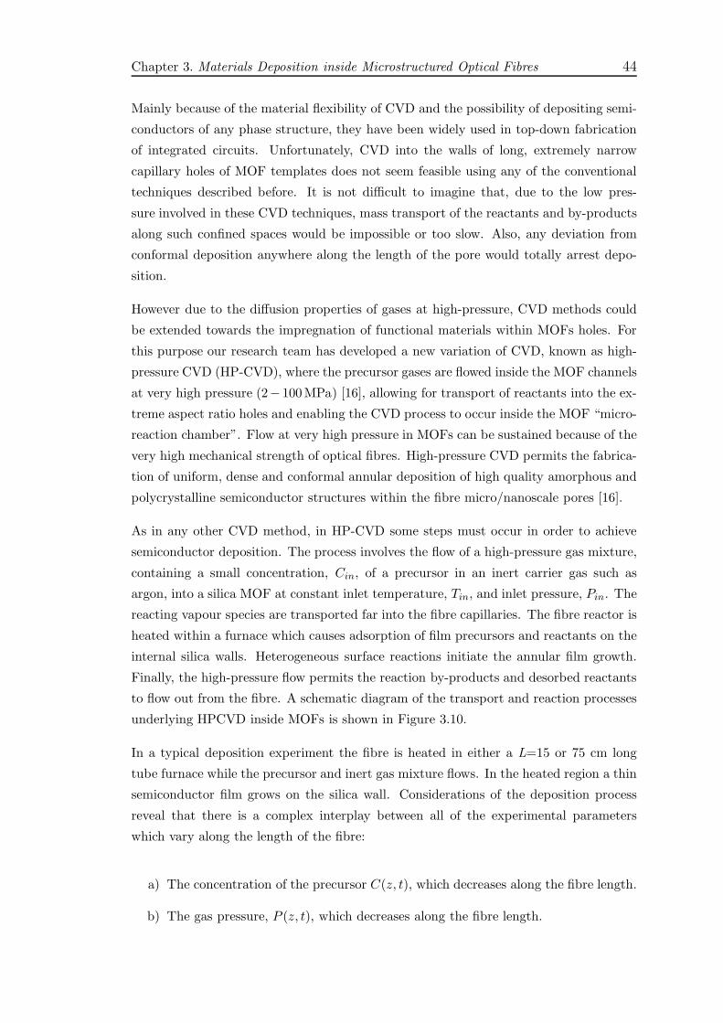
Chapter 3. Materials Deposition inside Microstructured Optical Fibres 44
Mainly because of the material flexibility of CVD and the possibility of depositing semi-
conductors of any phase structure, they have been widely used in top-down fabrication
of integrated circuits. Unfortunately, CVD into the walls of long, extremely narrow
capillary holes of MOF templates does not seem feasible using any of the conventional
techniques described before. It is not difficult to imagine that, due to the low pres-
sure involved in these CVD techniques, mass transport of the reactants and by-products
along such confined spaces would be impossible or too slow. Also, any deviation from
conformal deposition anywhere along the length of the pore would totally arrest depo-
sition.
However due to the diffusion properties of gases at high-pressure, CVD methods could
be extended towards the impregnation of functional materials within MOFs holes. For
this purpose our research team has developed a new variation of CVD, known as high-
pressure CVD (HP-CVD), where the precursor gases are flowed inside the MOF channels
at very high pressure (2− 100MPa) [16], allowing for transport of reactants into the ex-
treme aspect ratio holes and enabling the CVD process to occur inside the MOF “micro-
reaction chamber”. Flow at very high pressure in MOFs can be sustained because of the
very high mechanical strength of optical fibres. High-pressure CVD permits the fabrica-
tion of uniform, dense and conformal annular deposition of high quality amorphous and
polycrystalline semiconductor structures within the fibre micro/nanoscale pores [16].
As in any other CVD method, in HP-CVD some steps must occur in order to achieve
semiconductor deposition. The process involves the flow of a high-pressure gas mixture,
containing a small concentration, Cin, of a precursor in an inert carrier gas such as
argon, into a silica MOF at constant inlet temperature, Tin, and inlet pressure, Pin. The
reacting vapour species are transported far into the fibre capillaries. The fibre reactor is
heated within a furnace which causes adsorption of film precursors and reactants on the
internal silica walls. Heterogeneous surface reactions initiate the annular film growth.
Finally, the high-pressure flow permits the reaction by-products and desorbed reactants
to flow out from the fibre. A schematic diagram of the transport and reaction processes
underlying HPCVD inside MOFs is shown in Figure 3.10.
In a typical deposition experiment the fibre is heated in either a L=15 or 75 cm long
tube furnace while the precursor and inert gas mixture flows. In the heated region a thin
semiconductor film grows on the silica wall. Considerations of the deposition process
reveal that there is a complex interplay between all of the experimental parameters
which vary along the length of the fibre:
a) The concentration of the precursor C(z, t), which decreases along the fibre length.
b) The gas pressure, P (z, t), which decreases along the fibre length.
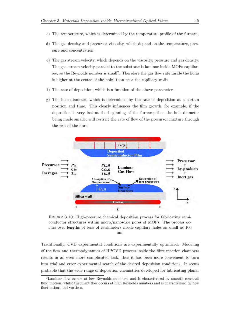
Chapter 3. Materials Deposition inside Microstructured Optical Fibres 45
c) The temperature, which is determined by the temperature profile of the furnace.
d) The gas density and precursor viscosity, which depend on the temperature, pres-
sure and concentration.
e) The gas stream velocity, which depends on the viscosity, pressure and gas density.
The gas stream velocity parallel to the substrate is laminar inside MOFs capillar-
ies, as the Reynolds number is small2. Therefore the gas flow rate inside the holes
is higher at the centre of the holes than near the capillary walls.
f) The rate of deposition, which is a function of the above parameters.
g) The hole diameter, which is determined by the rate of deposition at a certain
position and time. This clearly influences the film growth, for example, if the
deposition is very fast at the beginning of the furnace, then the hole diameter
being made smaller will restrict the rate of flow of the precursor mixture through
the rest of the fibre.
Figure 3.10: High-pressure chemical deposition process for fabricating semi-conductor structures within micro/nanoscale pores of MOFs. The process oc-curs over lengths of tens of centimeters inside capillary holes as small as 100
nm.
Traditionally, CVD experimental conditions are experimentally optimized. Modeling
of the flow and thermodynamics of HPCVD process inside the fibre reaction chambers
results in an even more complicated task, thus it has been more convenient to turn
into trial and error experimental search of the desired deposition conditions. It seems
probable that the wide range of deposition chemistries developed for fabricating planar
2Laminar flow occurs at low Reynolds numbers, and is characterised by smooth constantfluid motion, whilst turbulent flow occurs at high Reynolds numbers and is characterised by flowfluctuations and vortices.

Chapter 3. Materials Deposition inside Microstructured Optical Fibres 46
structures can be adopted for HPCVD [149], allowing the incorporation of many different
materials inside optical fibres. At the present time we have demonstrated the deposition
of amorphous and polycrystalline silicon, germanium and GeS2 by this method.
Finally, the danger associated with the very high pressure used in the process and the
toxic and explosive precursors is negligible in view of the small volume of the capillary
holes, which makes the process safe, practical and convenient.
3.5.1 High-Pressure CVD of Silicon inside MOFs
In the last century silicon has become the most important material in microelectronics
and a large number of different CVD methods have been explored for the deposition
of silicon layers onto planar substrates. CVD plays the important role of providing the
thin silicon film in which the active devices, ranging from complicated IC to cheap solar
cells, are patterned by lithography and etching methods. Two CVD techniques have
emerged as being the most useful and both have achieved a massive commercial impact.
These are the pyrolysis of silane (SiH4) and the hydrogen reduction of silicon tetrachlo-
ride (SiCl4) [122]. From these two techniques the one involving SiCl4 is advantageous
for top-down fabrication because it allows the growth of very high quality silicon at
convenient rates (µm/min). However, for the purposes of this thesis, where we require
to grow silicon micro/nanowires inside MOF templates, it is more convenient to use
the direct pyrolysis of silane. This is because the reactions involving (SiCl4) occur at
higher temperatures and silane reactions are more simple as they produce only one light
by-product (hydrogen).
In a typical HP-CVD experiment a high pressure gas mixture of 5% silicon precursor
SiH4 and 95% carrier gas, argon, at a pressure of approximately 40MPa is contained in
a high-pressure stainless steel reservoir. The gas is configured to flow through MOFs
whose hole diameters may range from ∼ 50 nm to 50µm. Even though a very small
amount of silane precursor is used, the gas mixtures used in these experiment are very
toxic and explosive, so are always handled with extreme care.
The fibre is fed through a 75 cm long tube furnace which is heated from room temperature
to 750 C at a rate of 4 C/min. The polymer coating of the fibres is either stripped before
heating or burned off during heating. When a silane molecule strikes the internal silica
surface, it can either bounce off or be absorbed. If it is absorbed, and the temperature
is high enough to initiate its decomposition, it may decompose into Si and H2 with the
later going back into the gas phase and being carried away from the reaction zone by
the fresh gas flow. Alternatively, H2 can diffuse out through the silica walls [150]. The
silicon left behind can build up as a thin amorphous silicon film on the MOF’s inner

Chapter 3. Materials Deposition inside Microstructured Optical Fibres 47
Figure 3.11: HP-CVD process for deposition of silicon wires inside micro/-nanoscale capillaries of MOFs using silane precursor. The high-pressure flowallows for transport of reactants deep inside the extreme aspect holes and en-
ables uniform, dense and conformal annular deposition of silicon.
silica walls (see Figure 3.11). As growth proceeds, a remarkably uniform tube forms.
As the temperature exceeds the crystallisation point of ∼ 700 C, crystalline grains then
nucleate and grow. The gas flow during the deposition can be monitored by placing the
fibre output into a mineral spirits liquid and examining the rate of bubble formation.
Figure 3.12: SEM micrographs of silicon annular deposition by HP-CVDmethod within micro/nano sized MOFs. a) 6µm diameter silica capillary filledwith silicon. The internal hole diameter after the deposition is only 1µm. Theinset shows the whole structure for clarity, scale bars are 2µm and 20µm re-spectively. b) silicon within a 2µm silica capillary, scale bar 1µm. c) Arrayof filled nanoscale holes, scale bar is 3µm (see Figure 2.4 for fibre template).
d) Twin hole MOF with 30µm diameter lateral holes, scale bar is 100µm
Scanning electron microscopy cross-sections, every centimetre along the length of capil-
laries filled with silicon, have been collected. It is observed that deposition is achieved

Chapter 3. Materials Deposition inside Microstructured Optical Fibres 48
even in sub 10 nm holes, indicating that substantive fluid flow must have occurred
through centimetres long nanoscale channels. Figure 3.12 shows SEM cross-sections
of different silicon-filled MOFs whose capillary holes range from ∼ 400 nm to ∼ 30µm.
Deposition within MOF with a honeycomb pattern, as shown in Figure 3.13, results in
several high aspect ratio silicon wires that can be released from the silica template by
HF etching. To our knowledge, the silicon wires fabricated in this way are the highest
aspect ratio silicon structure fabricated by any method.
Figure 3.13: SEM micrographs of silicon annular deposition by the HP-CVDmethod within a honeycomb MOF. a) MOF template before silicon deposition,scale bars is 2µm. b) silicon deposition inside a honeycomb MOF, scale bar is2µm c) Another example of silicon deposition within the holes of a honeycombfibre, scale bar is 5µm. d) The resulting tubes are released by etching the silica
template, scale bar is 50µm and inset is 1µm
The key issue to obtain conformal and homogeneous deposition is that silicon must
be deposited in the amorphous phase and then, by a post deposition thermal process,
crystallization is achieved. This allows the thin amorphous layer to follow the complex
geometry of the template which cannot be done by crystal grains. To investigate this,
two fibres attached to independent reservoirs were fed through a furnace. The pressure
and concentration of both precursor reservoirs was the same. The furnace temperature
was increased from room temperature to 750 C and the precursor was allowed to flow
through one fibre whereas the other other reservoir was not opened until the furnace
temperature was 550 C. It can be seen in Figure 3.14, that the deposition in the
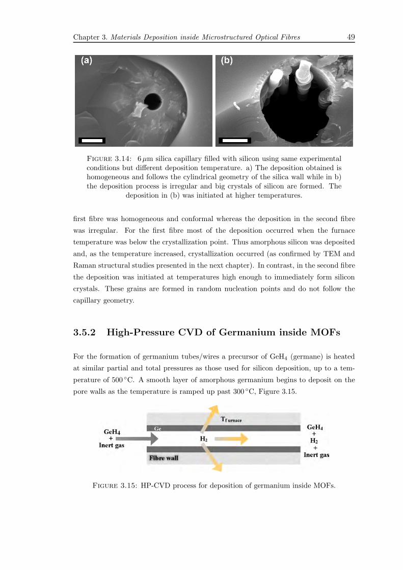
Chapter 3. Materials Deposition inside Microstructured Optical Fibres 49
Figure 3.14: 6µm silica capillary filled with silicon using same experimentalconditions but different deposition temperature. a) The deposition obtained ishomogeneous and follows the cylindrical geometry of the silica wall while in b)the deposition process is irregular and big crystals of silicon are formed. The
deposition in (b) was initiated at higher temperatures.
first fibre was homogeneous and conformal whereas the deposition in the second fibre
was irregular. For the first fibre most of the deposition occurred when the furnace
temperature was below the crystallization point. Thus amorphous silicon was deposited
and, as the temperature increased, crystallization occurred (as confirmed by TEM and
Raman structural studies presented in the next chapter). In contrast, in the second fibre
the deposition was initiated at temperatures high enough to immediately form silicon
crystals. These grains are formed in random nucleation points and do not follow the
capillary geometry.
3.5.2 High-Pressure CVD of Germanium inside MOFs
For the formation of germanium tubes/wires a precursor of GeH4 (germane) is heated
at similar partial and total pressures as those used for silicon deposition, up to a tem-
perature of 500 C. A smooth layer of amorphous germanium begins to deposit on the
pore walls as the temperature is ramped up past 300 C, Figure 3.15.
Figure 3.15: HP-CVD process for deposition of germanium inside MOFs.

Chapter 3. Materials Deposition inside Microstructured Optical Fibres 50
Figure 3.16: Germanium integrated into MOFs. (a) SEM cross-section of agermanium tube in a 2µm silica capillary, scale bar is 500 nm (b) Germaniumdeposited in a 1µm pore, the central hole is ∼ 25 nm in diameter, scale bar is200 nm. (c) A germanium wire etched out of silica MOF template, scale bar is2µm. (d) Field emission SEM cross section of a germanium nanotube within a
MOF nanotemplate, scale bar is 100 nm, from [16].
Crystalline grains then nucleate and grow as the temperature exceeds the crystallization
point of 375 C, which is much lower than that of silicon ∼ 700 C. As growth proceeds,
again, a remarkably uniform tube forms (see Figure 3.16); as it fills with germanium,
a 1µm diameter pore can be narrowed by a factor of 100 down to 25 nm or smaller,
tapering open gradually over a deposition length of 70 cm. Silica capillaries drawn to
a 100 nm diameter were also successfully filled with germanium to form nanotubes over
macroscopic lengths of up to 30 cm, with an inner diameter of less than 10 nm (Figure
3.16).
Deposition into more highly structured pores reveals additional information about this
conformal filling. When a large-air-fraction fibre with a honeycomb pattern of holes is
filled, a spatially ordered array of hexagonal germanium tubes is formed (Figure 3.17).
The interior vertices of the hexagonal holes, originally defined by the rounded silica
template, actually sharpen as growth proceeds. If uniform inward motion of the surface,
along the normal, during deposition is assumed, then the rounded corners of a polygon
will become sharp as the thickness of the deposited layer exceeds the radius of curva-
ture of the corner, as illustrated in Figure 3.17c. The resulting faceted tubes resemble

Chapter 3. Materials Deposition inside Microstructured Optical Fibres 51
lithographically patterned micro and nanostructures but are formed in a simple single-
stage deposition. This uniform annular growth, down to very small inner diameters,
with sharp geometric features, is particularly striking when one considers that the ger-
manium is polycrystalline, with a grain size much larger than the dimensions of these
features.
The remarkably simple fabrication of 3D semiconductor structures via the HP-CVD
deposition of semiconductors within holey fibres templates introduces a new class of
optically and electronically controllable in-fibre metamaterials. The following chapter
explores the exciting optical and electrical properties of these new semiconductor mod-
ified optical fibres.
Figure 3.17: SEM micrographs showing of a 2µm honeycomb MOF filledwit (a) thin homogeneous layer of germanium, scale bar is 300 nm (b) thickconformal layer of germanium, scale bar is 1µm. (c) Schematic showing surfacesgrowing inward in a direction perpendicular to the silica walls (green arrows).When the deposition reaches the thickness indicated by the green hexagon, therounded corners have vanished and the cross-section is a perfect hexagon [16].

Chapter 3. Materials Deposition inside Microstructured Optical Fibres 52
3.6 Vapor Liquid Solid Growth of Single-Crystal
Silicon inside MOFs
Single crystal semiconductors have superior photonic and electronic properties com-
pared with poly-crystalline and amorphous semiconductors, which makes them the base
materials for electronic and optoelectronic devices. During the last decades, several
single crystal growth methods have been investigated and today epitaxial growth consti-
tutes the primary process toward the construction of most microelectronic circuits and
MEMS. Epitaxial techniques arrange atoms in single-crystal fashion upon a seed crystal
substrate so that the lattice of the newly grown film duplicates that of the substrate.
Epitaxial growth of silicon occurs on a substrate with a closely matched lattice constant
and thermal expansion coefficient [118].
Although CVD has been used for the deposition of epitaxial single crystal silicon, the use
of HP-CVD is not successful in growing single crystal silicon inside MOFs. This is mainly
because of the lattice mismatch between the silica template and silicon. An alternative
method, Vapour-Liquid-Solid (VLS) growth has been investigated for monocrystal for-
mation inside MOFs. VLS requires the presence of a metal catalyst which has a low
eutectic temperature with silicon. Since the first demonstration of VLS growth of sili-
con [151], gold has commonly been used as the VLS seed. Moreover the Si-Au eutectic
temperature is ∼ 360 C, this can be easily supported by silica fibres, making it possi-
ble to carry out the process inside MOFs. Recently VLS has been applied for growing
single crystal silicon, germanium and compound semiconductor nanowires which have
found many applications as building blocks for nanoscale electronic, optoelectronic and
NEMS devices [18, 152, 153, 154, 155, 156, 157]. The extension of this technique to the
templated growth of semiconductor wires within MOFs could result in many interesting
applications.
VLS growth of silicon wires from a gold seed can be described as a four-step process. (1)
A gold particle is deposited onto a surface and heated above the eutectic temperature.
The seed will define the dimensions and geometry of the silicon wire. (2) A silicon vapour
precursor (SiH4) interacts with the gold seed which acts as a catalyst to decompose the
precursor. The reaction produces Si and H2 gas as a by-product on the gold surface. The
silicon diffuses into the gold particle and forms a Si-Au alloy. As the silicon concentration
increases, the melting temperature of the alloy decreases. The silicon concentration
increases and the alloy particle is saturated. (3) At the saturation point no more silicon
can diffuse into the gold and instead a solid silicon particle nucleates on the substrate.
(4) Finally single crystal wire grows from the nucleation point with a liquid Si-Au droplet
at the tip [150].

Chapter 3. Materials Deposition inside Microstructured Optical Fibres 53
Figure 3.18: Schematic of laser-assisted supercritical fluid deposition of goldparticles inside MOF capillaries (a,b). Focused laser radiation enables the de-position of gold from a flowing supercritical fluid precursor at precise locationsalong the fibre. (b) Microscope image of gold particles deposited in a 2µm
capillary. [150, 16]
The principle of template-directed VLS requires the deposition of gold particles inside the
MOF template and then the flow of silicon precursor inside the pores. The transparency
of silica MOFs permits gold deposition inside MOFs by laser assisted decomposition of a
gold organometallic precursor (Me2Au(tfac)) which is dissolved in scCO2. Laser-Assisted
Supercritical Fluid Deposition (LASCFD) provides the ability to create gold particles
at specific locations in the fibre, which is extremely important to achieve VLS growth.
If the case where a gold seed is deposited within a large area is consider, then the silicon
wires would grow at any location which will easily block the precursor flow and arrest
the deposition. A diagram of the LASCFD process of gold particles is shown in Figure
3.18a,b. Radiation from an argon-ion laser, operating at 514 nm, is focused with a 100×objective at the desired position inside the capillary holes. As the gold precursor passes
through the illuminated region it is photolytically decomposed and forms solid gold, plus
by-products which are carried out of the fibre by the high pressure flow. Figure 3.18c
shows a 1.6µm capillary fibre which has been patterned with gold particles at different
positions.
Once a gold seed is deposited inside the capillary the VLS process takes place by heating
up the capillary above 360 C while flowing high-pressure silane in a helium carrier gas.
The high-pressure VLS process is shown in Figure 3.19. During the growth process
is extremely important to remove the reaction by-products away from the gold seed.
Although most of the reaction by-products are carried out of the fibre by the gas flow,
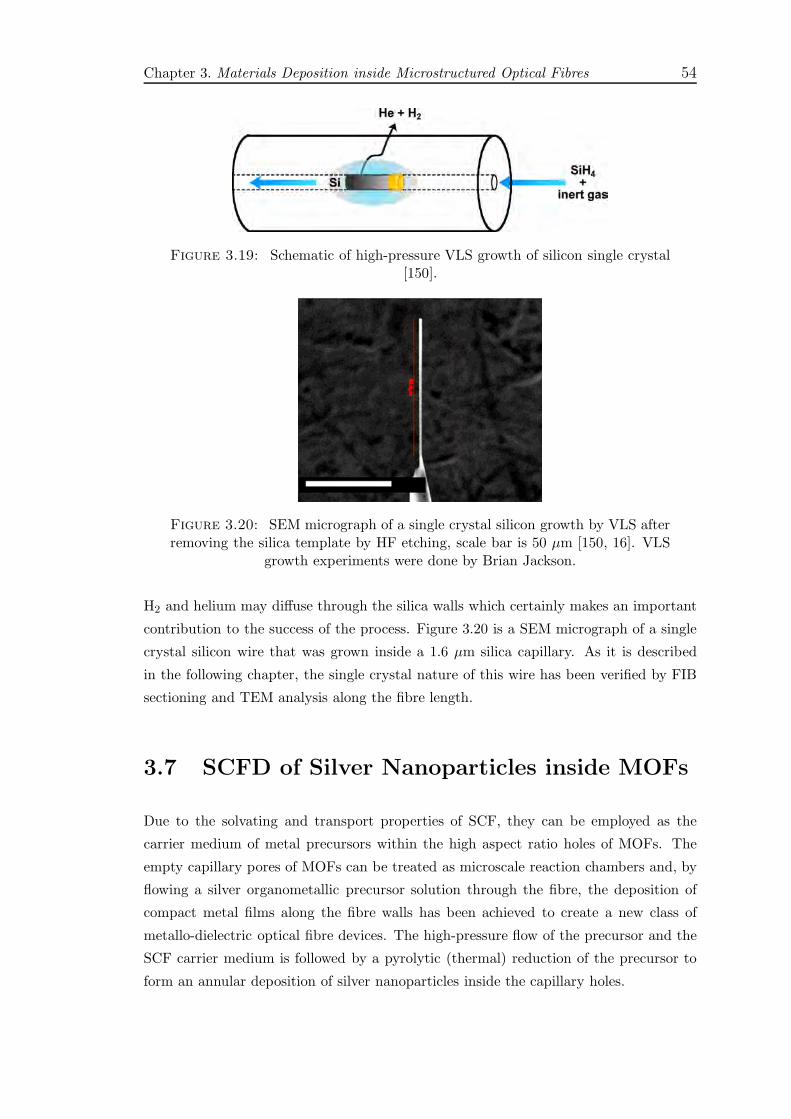
Chapter 3. Materials Deposition inside Microstructured Optical Fibres 54
Figure 3.19: Schematic of high-pressure VLS growth of silicon single crystal[150].
Figure 3.20: SEM micrograph of a single crystal silicon growth by VLS afterremoving the silica template by HF etching, scale bar is 50 µm [150, 16]. VLS
growth experiments were done by Brian Jackson.
H2 and helium may diffuse through the silica walls which certainly makes an important
contribution to the success of the process. Figure 3.20 is a SEM micrograph of a single
crystal silicon wire that was grown inside a 1.6 µm silica capillary. As it is described
in the following chapter, the single crystal nature of this wire has been verified by FIB
sectioning and TEM analysis along the fibre length.
3.7 SCFD of Silver Nanoparticles inside MOFs
Due to the solvating and transport properties of SCF, they can be employed as the
carrier medium of metal precursors within the high aspect ratio holes of MOFs. The
empty capillary pores of MOFs can be treated as microscale reaction chambers and, by
flowing a silver organometallic precursor solution through the fibre, the deposition of
compact metal films along the fibre walls has been achieved to create a new class of
metallo-dielectric optical fibre devices. The high-pressure flow of the precursor and the
SCF carrier medium is followed by a pyrolytic (thermal) reduction of the precursor to
form an annular deposition of silver nanoparticles inside the capillary holes.

Chapter 3. Materials Deposition inside Microstructured Optical Fibres 55
Figure 3.21: Schematic (not to scale) of the experimental set-up for the de-position of silver nanoparticles inside microstructured optical fibres. The de-composition of the organometallic precursor to form a compact silver film onthe silica walls takes place within the heated area. The chemical structure ofthe organometallic silver precursor together with the decomposition process is
shown in the inset.
Figure 3.22: SEM micrographs showing a range of silver deposition profilesobtained by tuning the experimental parameters. (A) Deposition time = 0.5 hrswith a precursor concentration of 5mg/ml; 1µm scale bar. (B) Deposition time= 0.5 hrs with a precursor concentration of 10mg/ml; scale bar is 1µm. (C)Deposition time = 2 hrs with a precursor concentration of 10mg/ml; scale barsare 2µm and 20µm on the inset. (D) Deposition time = 3 hrs with a precursor
concentration of 15mg/ml; 2µm scale bar.
The chosen precursor for the formation of silver films is Ag(hfac)(1, 5-COD) (hfac=

Chapter 3. Materials Deposition inside Microstructured Optical Fibres 56
1, 1, 1, 5, 5, 5-hexafluoroacetylacetonato, COD = cyclo-octadiene) due to its high solu-
bility in organic solvents, such as n-heptane and scCO2, and also due to the desirable
low decomposition temperature (200C) of this complex. The experimental chemicals,
Ag(hfac)(1, 5-COD) and n-heptane (HPLC grade), are purchased from Sigma-Aldrich
and used as received. Figure 3.21 shows a schematic of the experimental set-up used in
SCF deposition inside MOFs. Ag(hfac)(1, 5-COD) is dissolved in n-heptane (typically
up to 15mg/ml) and the solution is flowed through the optical fibre at around 17MPa
by a high performance liquid-chromatography pump (HPLCP). Once again, due to the
small volume contained in the fibres, the amount of precursor required for the deposi-
tion is tiny making the process safe even at the high pressures used in the experiments.
The optical fibre is then fed through a 10 cm long heating cartridge with temperature
control and HiP taps (High Pressure Equipment Company, USA) are used to control
the precursor solution flow rate. As the precursor flows through the fibre, the furnace is
heated up to 200C to initiate the decomposition of the precursor into pure silver and
by-products. During the first few minutes of the process, metal begins to deposit as
small islands onto the capillary walls. As the deposition time increases, the nanoparti-
cles serve as nucleation points allowing the formation of thin granular films along the
heated length. Run times for this process range between 0.5− 3 hours depending on the
desired deposition profile and on the fibre structure.
After the deposition, any decomposed ligands can be easily removed by the same sol-
vent, leaving high purity silver grains inside the fibre. If required, supercritical CO2
can be flowed through the optical fibre to remove any trace of precursor (or any other
unwanted by-products) left inside the holes. Figure 3.22 displays different silver coatings
achieved by tuning the experimental parameters such as the deposition time, tempera-
ture, precursor concentration and flow rate. The silver nanoparticles diameter can be
finely controlled from tens of nanometres to hundred nanometres, and the silver coating
thickness up to a few micrometres. In all cases we observed a uniform filling of the holes
across the fibre structure, as illustrated by the inset of Figure 3.22c.
The optical characterisation of silver-modified MOFs is presented in Chapter 7, they
have proven to be excellent substrates for surface enhanced Raman scattering.
3.8 SCFD of Polymers inside MOFs
Holey fibres filled with polymers present some attractive tuneable optical properties
[158]. SCF deposition of polymer inside MOFs is advantageous, compared to other low
pressure polymer impregnation methods previously used by other research groups, in
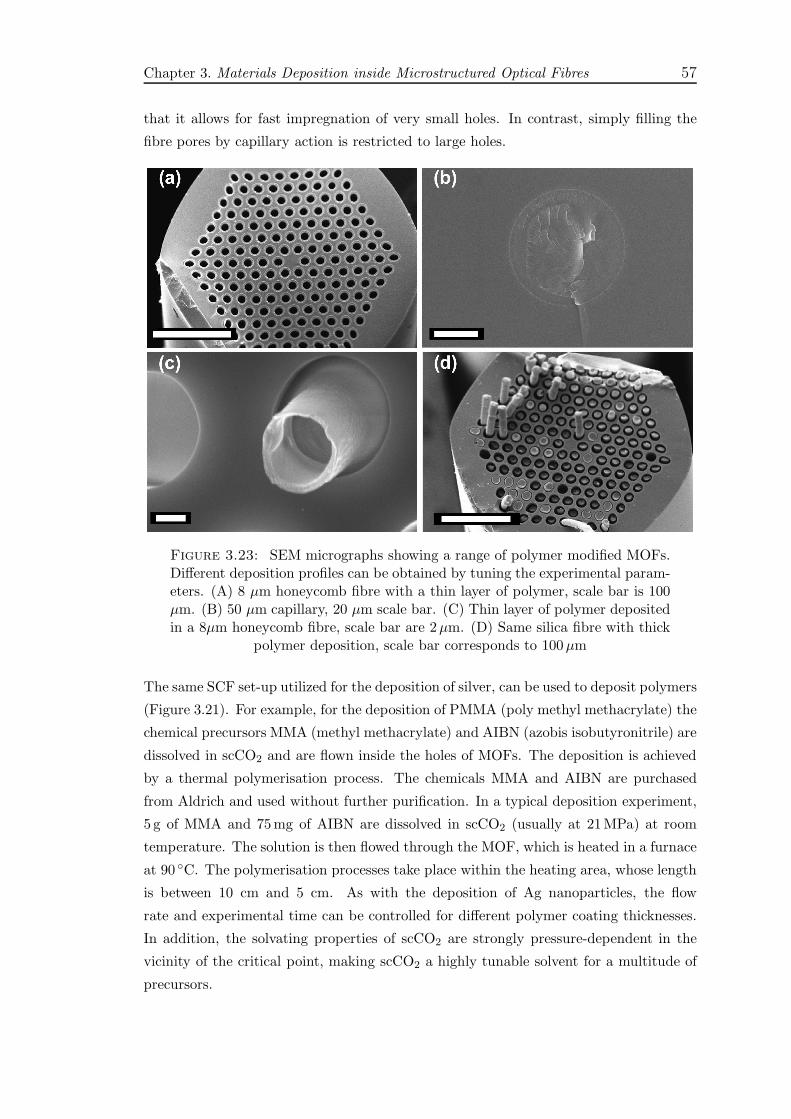
Chapter 3. Materials Deposition inside Microstructured Optical Fibres 57
that it allows for fast impregnation of very small holes. In contrast, simply filling the
fibre pores by capillary action is restricted to large holes.
Figure 3.23: SEM micrographs showing a range of polymer modified MOFs.Different deposition profiles can be obtained by tuning the experimental param-eters. (A) 8 µm honeycomb fibre with a thin layer of polymer, scale bar is 100µm. (B) 50 µm capillary, 20 µm scale bar. (C) Thin layer of polymer depositedin a 8µm honeycomb fibre, scale bar are 2µm. (D) Same silica fibre with thick
polymer deposition, scale bar corresponds to 100µm
The same SCF set-up utilized for the deposition of silver, can be used to deposit polymers
(Figure 3.21). For example, for the deposition of PMMA (poly methyl methacrylate) the
chemical precursors MMA (methyl methacrylate) and AIBN (azobis isobutyronitrile) are
dissolved in scCO2 and are flown inside the holes of MOFs. The deposition is achieved
by a thermal polymerisation process. The chemicals MMA and AIBN are purchased
from Aldrich and used without further purification. In a typical deposition experiment,
5 g of MMA and 75mg of AIBN are dissolved in scCO2 (usually at 21MPa) at room
temperature. The solution is then flowed through the MOF, which is heated in a furnace
at 90 C. The polymerisation processes take place within the heating area, whose length
is between 10 cm and 5 cm. As with the deposition of Ag nanoparticles, the flow
rate and experimental time can be controlled for different polymer coating thicknesses.
In addition, the solvating properties of scCO2 are strongly pressure-dependent in the
vicinity of the critical point, making scCO2 a highly tunable solvent for a multitude of
precursors.

Chapter 3. Materials Deposition inside Microstructured Optical Fibres 58
The SEM micrographs in Figure 3.23 show some examples of the deposition profiles that
can be obtained. Holes ranging from 2−50µm have been successfully impregnated with
thin polymer coating or completely filled.

Chapter 4
Semiconductor Modified Optical
Fibres
As described in Chapter 3, using HP-CVD we have for the first time to our knowledge,
achieved the fabrication of optical fibres with bulk crystalline semiconductor inclusions.
A critical issue of this research has been to characterise the physical properties of silicon
and germanium deposited inside by HP-CVD. In this chapter the crystalline structure
of resulting semiconductor tubes/wires are studied with TEM and Raman spectroscopy.
Electrical transport and optical transmission measurements are used to gather informa-
tion on the material quality and the prospects of their use. Semiconductor-filled MOFs
provide the opportunity to exploit various optical and electronic processes to control and
manipulate guided light. The first results in this direction are presented in this chapter,
with a FET and waveguides being the main devices which have at the time of writing
been demonstrated.
4.1 Structural Characterisation of Semiconduc-
tor MOFs
This section describes the theoretical and experimental background of two techniques
used to characterise the crystalline structure of semiconductor-filled MOFs. These tech-
niques are transmission electron microscopy (TEM) and Raman spectroscopy. The char-
acterisation of silicon and germanium in-fibre wires/tubes requires the removal of the
semiconductor structures from the silica MOF/template to have access to the deposited
material itself. For this purpose it has been important to develop an etching method by
which only a small length of the semiconductor wire protrudes from the silica template.
59

Chapter 4. Semiconductor Optical Fibres 60
The silica template is selectively etched with 48% hydrofluoric acid (HF). For the etch-
ing process, semiconductor-filled fibres are mounted on a Teflonr holder with 125µm
v-grooves. The holder is then attached to a container and a short section of the fibre is
then in contact with HF acid. Figure 4.1 is an illustration of the fibre holder and the
acid container.
Figure 4.1: Schematic diagram (not to scale) of the experimental etching setup. The etching procedure only requires around 2ml of HF acid, and it lastsfor approximately 30 minutes. Because of the small amount of HF used, the
process is safe, however, care must be taken.
Once the fibres are introduced into the HF acid the process, is continuously monitored
under a microscope and etching is finished when the desired length of silica has been
removed. Finally the fibres are washed with distilled water, to remove any acid residue,
and are mounted onto glass slides for further characterisation. Figure 4.2 shows some
etched fibres, illustrating the precise control that has been obtained over the etching
process.
Figure 4.2: Microscope images of etched MOFs. (a) 5µm silica capillaryfilled with germanium, the germanium tube sticks out ≈ 10µm from the silicatemplate, scale bar is 20µm. Inset: cross-sectional view of the etched tube,scale bar 10µm. (b) 2µm silicon tube, scale bar is 20µm. The inset is the same
capillary fibre after etching a longer length.
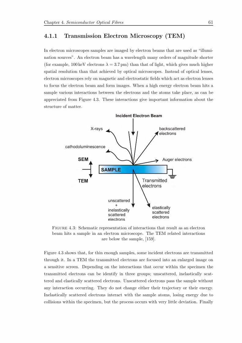
Chapter 4. Semiconductor Optical Fibres 61
4.1.1 Transmission Electron Microscopy (TEM)
In electron microscopes samples are imaged by electron beams that are used as “illumi-
nation sources”. An electron beam has a wavelength many orders of magnitude shorter
(for example, 100 keV electrons λ = 3.7 pm) than that of light, which gives much higher
spatial resolution than that achieved by optical microscopes. Instead of optical lenses,
electron microscopes rely on magnetic and electrostatic fields which act as electron lenses
to focus the electron beam and form images. When a high energy electron beam hits a
sample various interactions between the electrons and the atoms take place, as can be
appreciated from Figure 4.3. These interactions give important information about the
structure of matter.
Figure 4.3: Schematic representation of interactions that result as an electronbeam hits a sample in an electron microscope. The TEM related interactions
are below the sample, [159].
Figure 4.3 shows that, for thin enough samples, some incident electrons are transmitted
through it. In a TEM the transmitted electrons are focused into an enlarged image on
a sensitive screen. Depending on the interactions that occur within the specimen the
transmitted electrons can be identify in three groups; unscattered, inelastically scat-
tered and elastically scattered electrons. Unscattered electrons pass the sample without
any interaction occurring. They do not change either their trajectory or their energy.
Inelastically scattered electrons interact with the sample atoms, losing energy due to
collisions within the specimen, but the process occurs with very little deviation. Finally

Chapter 4. Semiconductor Optical Fibres 62
elastically scattered electrons interact with the heavy atoms and their trajectory is af-
fected without losing any, or very little, energy. They are deflected through wide angles
(typically 0.6-3 degree) by the interaction [159].
As described by Bragg’s Diffraction Law, the electron beam interacts with crystalline
samples in a very specific way. If the sample is crystalline its atoms are geometrically
arranged in a periodic pattern which has certain planes with a high density of atoms
that act as reflection planes (see Appendix A). Suppose that a coherent electron beam is
reflected (or diffracted) from parallel planes of the crystal, each plane reflecting a small
fraction of the energy. Any reflected waves, which are in phase with each other, will
interfere constructively and form a diffraction pattern. Whereas any scattered waves,
which are not in phase, will not be reinforced. The condition for constructive interference
is given by Bragg’s Law:
2d sin θ = nλ, (4.1)
where θ is the incident angle, d is the lattice spacing between crystal planes, n is an
integer number and λ is the wavelength of the electron wave. This relation is illustrated
in Figure 4.4. It should be noted that the incident and reflected beams form an angle
of 2θ with each other.
Figure 4.4: Bragg’s Law of diffraction from parallel planes. The electron beamis reflected from two crystal planes which contain a high density of atoms, thespacing between them is d. If equation 4.1 is satisfied, the beam reflected by
the lowest plane reinforces the reflection from the first plane [56].
Consider the case when a collimated electron beam passes through a crystal at a correct
angle of incidence for diffraction to occur from a set of lattice planes. The elastically
scattered electrons are deviated from the incident beam by an angle 2θ and will result
in a bright spot in the diffraction pattern. If a sensitive film is placed at a distance L
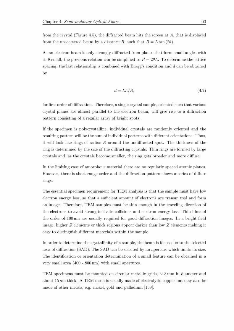
Chapter 4. Semiconductor Optical Fibres 63
from the crystal (Figure 4.5), the diffracted beam hits the screen at A, that is displaced
from the unscattered beam by a distance R, such that R = L tan (2θ).
As an electron beam is only strongly diffracted from planes that form small angles with
it, θ small, the previous relation can be simplified to R = 2θL. To determine the lattice
spacing, the last relationship is combined with Bragg’s condition and d can be obtained
by
d = λL/R, (4.2)
for first order of diffraction. Therefore, a single crystal sample, oriented such that various
crystal planes are almost parallel to the electron beam, will give rise to a diffraction
pattern consisting of a regular array of bright spots.
If the specimen is polycrystalline, individual crystals are randomly oriented and the
resulting pattern will be the sum of individual patterns with different orientations. Thus,
it will look like rings of radius R around the undiffracted spot. The thickness of the
ring is determined by the size of the diffracting crystals. Thin rings are formed by large
crystals and, as the crystals become smaller, the ring gets broader and more diffuse.
In the limiting case of amorphous material there are no regularly spaced atomic planes.
However, there is short-range order and the diffraction pattern shows a series of diffuse
rings.
The essential specimen requirement for TEM analysis is that the sample must have low
electron energy loss, so that a sufficient amount of electrons are transmitted and form
an image. Therefore, TEM samples must be thin enough in the traveling direction of
the electrons to avoid strong inelastic collisions and electron energy loss. Thin films of
the order of 100 nm are usually required for good diffraction images. In a bright field
image, higher Z elements or thick regions appear darker than low Z elements making it
easy to distinguish different materials within the sample.
In order to determine the crystallinity of a sample, the beam is focused onto the selected
area of diffraction (SAD). The SAD can be selected by an aperture which limits its size.
The identification or orientation determination of a small feature can be obtained in a
very small area (400 - 800 nm) with small apertures.
TEM specimens must be mounted on circular metallic grids, ∼ 3mm in diameter and
about 15µm thick. A TEM mesh is usually made of electrolytic copper but may also be
made of other metals, e.g. nickel, gold and palladium [159].
Chapter 4. Semiconductor Optical Fibres 64
2θ
Thin crystal
Diffractedbeam
Thin crystal
Undiffractedbeam
L
Film R
Incidentbeam
O A
Figure 4.5: Basic elements of an electron diffraction camera. Undiffractedelectrons travel directly to point O in the photographic screen, while diffracted
beams from the sample arrive at A in the screen, from reference [160].
4.1.1.1 Diffraction Patterns of Silicon MOFs
Silicon was deposited in a honeycomb fibre using the HP-CVD method (∼ 14.5MPa
with ∼ 750 kPa partial pressure of SiH4). A SEM cross-sectional micrograph of the
resulting fibre is shown in Figure 4.6. This sample was taken from a position along the
fibre length 4 cm away from the furnace entrance (see Section 3.5.1 for experimental
deposition details). The sample was obtained from very close to the furnace entrance
because previous SEM studies revealed that at this position the silicon tubes are very
thin. However, the MOF template is much thicker than the 100 nm thickness required
for TEM analysis and, thus, before attempting TEM analysis, the semiconductor wires
are released from the silica template. The silica cladding of this sample was etched out
with HF acid. The free wires were washed with distilled water and chopped into pieces
with metallic tweezers. Afterwards, the wires were suspended in isopropanol and picked
up with a pipette. They were then drop-cast on TEM copper grids and left to dry out.
With this procedure, the probability of finding a tube with a section thin enough for
diffraction analysis was low and many grids had to be prepared. The grids were loaded
onto a sample holder of the TEM.
A Philips EM 420 TEM microscope with camera length L = 480mm was used. The
samples were illuminated with a 120KeV (λ = 0.03349 A) electron beam. Figure 4.7a

Chapter 4. Semiconductor Optical Fibres 65
Figure 4.6: SEM micrograph of a honeycomb MOF with a thin silicon layeron the walls of the 2µm holes. The silicon tubes of this fibre were released from
the silica matrix and characterised by TEM studies; the scale bar is 5µm
is a bright field image of a silicon wire. It can be appreciated that this wire has some
bright regions that are thin enough for TEM studies. The red and yellow circles indicate
the selected areas for diffraction and the patterns are shown in Figures 4.7b and Figure
4.7c respectively. The aperture used in both cases was 400 nm. The SAD enclosed in
the red circle led to a set of broad and diffuse concentric rings, which clearly indicate
that the silicon in this area is amorphous with some nanocrystal phases.
The diffraction pattern from the area enclosed by the yellow circle in Figure 4.7a is
shown in Figure 4.7c. In this region, the diffraction rings are more defined with some
bright spots superimposed on them. This indicates that silicon within the selected area
is polycrystalline. The rings correspond to different lattice planes and can be assigned to
the silicon structure using equation (4.2). The rings indicated in the figure correspond
to lattice separations d = 3.135 A and d = 1.92 A and are associated with the (111) and
(220) lattice planes of silicon, with lattice constant a = 5.430 A.
Therefore, TEM analysis on this particular MOF revealed that the silicon tubes de-
posited under these experimental conditions contain polycrystalline and amorphous
phases. As will be described later, the crystalline structure of silicon is highly dependent
on the deposition conditions.
4.1.1.2 Diffraction Patterns of Germanium MOFs
In the first TEM experiments on germanium fibres the procedure used for sample prepa-
ration was the same as that described for silicon. Germanium was deposited in a hon-
eycomb fibre using the HP-CVD method (∼ 14MPa with ∼ 750 kPa partial pressure
of of GeH4). A SEM micrograph of this germanium fibre is shown in Figure 4.8. The

Chapter 4. Semiconductor Optical Fibres 66
Figure 4.7: (a) Bright field image of a 2µm silicon tube, the circles indicatethe SADs; the scale bar is 1µm. (b) SAD pattern obtained from amorphoussilicon with small crystalline phases, obtained from silicon within the red area.(c) “spotty ring” type of diffraction pattern obtained from polycrystalline silicon
from the yellow region in (a).
silica fibre template was etched out and the 2µm germanium tubes were released and
mounted on TEM grids.
Figure 4.9a is the bright field image of the deposited germanium and the grey circle
is the SAD whose diffraction pattern is shown in Figure 4.9b. The bright spots in
the diffraction pattern clearly indicate that the germanium wire is crystalline. Some
crystal planes can be identified in the image. Although a ‘spotty’ diffraction pattern
corresponds to single crystal material, the germanium wire is not monocrystalline and,
as the SAD is moved to different regions of the sample, the orientation of the planes
changes and a different diffraction pattern is obtained. Thus, the wire is composed of

Chapter 4. Semiconductor Optical Fibres 67
Figure 4.8: SEM micrograph of a honeycomb MOF with a 300 nm germaniumlayer deposited on the 2µm holes; scale bar is 5µm
Figure 4.9: (a) Bright field image of a 2µm germanium tube. The circle indi-cates the SADs; scale bar is 200 nm. (b) diffraction pattern showing crystalline
germanium and lattice planes.
polycrystalline material, with big crystal grains, and thus within a SAD there are only
a few large crystals.
In order to obtain a better understanding of the orientation and size of the crystals
it was necessary to have more control over the sample preparation. For this the silica
cladding of a germanium fibre was first removed with HF. Then a focused ion beam (FIB)
instrument was used to obtain thin cross sections from the fibres. The thin sample was
picked up with micro-manipulators and further thinned with FIB. When the sample was
thin enough for TEM analysis, it was mounted on a TEM grid. Some SEM micrographs
of the FIB sample preparation procedure are shown in Figure 4.10.
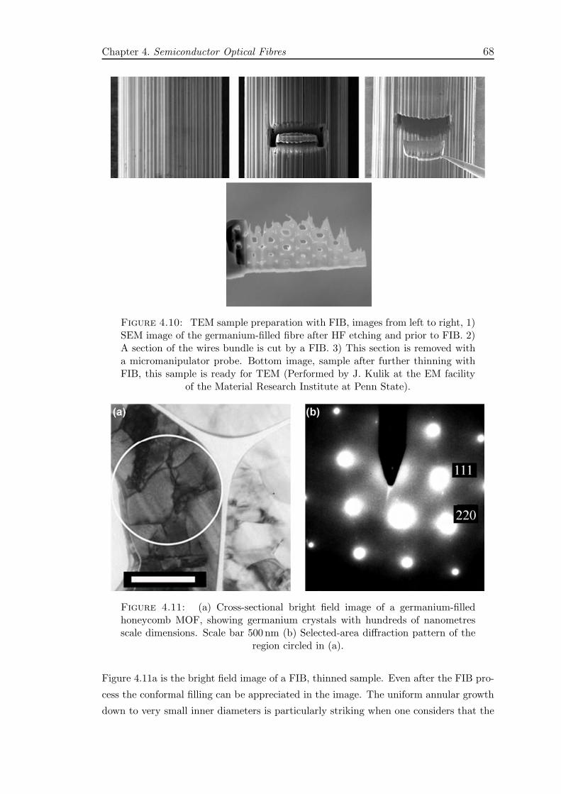
Chapter 4. Semiconductor Optical Fibres 68
Figure 4.10: TEM sample preparation with FIB, images from left to right, 1)SEM image of the germanium-filled fibre after HF etching and prior to FIB. 2)A section of the wires bundle is cut by a FIB. 3) This section is removed witha micromanipulator probe. Bottom image, sample after further thinning withFIB, this sample is ready for TEM (Performed by J. Kulik at the EM facility
of the Material Research Institute at Penn State).
Figure 4.11: (a) Cross-sectional bright field image of a germanium-filledhoneycomb MOF, showing germanium crystals with hundreds of nanometresscale dimensions. Scale bar 500 nm (b) Selected-area diffraction pattern of the
region circled in (a).
Figure 4.11a is the bright field image of a FIB, thinned sample. Even after the FIB pro-
cess the conformal filling can be appreciated in the image. The uniform annular growth
down to very small inner diameters is particularly striking when one considers that the
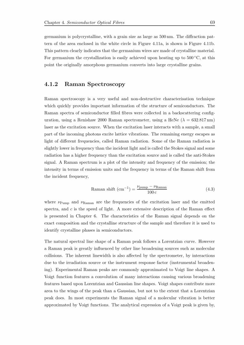
Chapter 4. Semiconductor Optical Fibres 69
germanium is polycrystalline, with a grain size as large as 500 nm. The diffraction pat-
tern of the area enclosed in the white circle in Figure 4.11a, is shown is Figure 4.11b.
This pattern clearly indicates that the germanium wires are made of crystalline material.
For germanium the crystallization is easily achieved upon heating up to 500 C, at this
point the originally amorphous germanium converts into large crystalline grains.
4.1.2 Raman Spectroscopy
Raman spectroscopy is a very useful and non-destructive characterisation technique
which quickly provides important information of the structure of semiconductors. The
Raman spectra of semiconductor filled fibres were collected in a backscattering config-
uration, using a Renishaw 2000 Raman spectrometer, using a HeNe (λ = 632.817 nm)
laser as the excitation source. When the excitation laser interacts with a sample, a small
part of the incoming photons excite lattice vibrations. The remaining energy escapes as
light of different frequencies, called Raman radiation. Some of the Raman radiation is
slightly lower in frequency than the incident light and is called the Stokes signal and some
radiation has a higher frequency than the excitation source and is called the anti-Stokes
signal. A Raman spectrum is a plot of the intensity and frequency of the emission; the
intensity in terms of emission units and the frequency in terms of the Raman shift from
the incident frequency,
Raman shift (cm−1) =νpump − νRaman
100 c(4.3)
where νPump and νRaman are the frequencies of the excitation laser and the emitted
spectra, and c is the speed of light. A more extensive description of the Raman effect
is presented in Chapter 6. The characteristics of the Raman signal depends on the
exact composition and the crystalline structure of the sample and therefore it is used to
identify crystalline phases in semiconductors.
The natural spectral line shape of a Raman peak follows a Lorentzian curve. However
a Raman peak is greatly influenced by other line broadening sources such as molecular
collisions. The inherent linewidth is also affected by the spectrometer, by interactions
due to the irradiation source or the instrument response factor (instrumental broaden-
ing). Experimental Raman peaks are commonly approximated to Voigt line shapes. A
Voigt function features a convolution of many interactions causing various broadening
features based upon Lorentzian and Gaussian line shapes. Voigt shapes contribute more
area to the wings of the peak than a Gaussian, but not to the extent that a Lorentzian
peak does. In most experiments the Raman signal of a molecular vibration is better
approximated by Voigt functions. The analytical expression of a Voigt peak is given by,

Chapter 4. Semiconductor Optical Fibres 70
V (x) =
∫ ∞−∞
H exp(−y2)
ω2
l+
h“
x−x0
ωg
”
−yi2 dy
∫ ∞−∞
exp(−y2)ω2
g+y2 dy, (4.4)
where V (x) is the Voigt function, ωl and ωg are the width of the Lorentzian and Gaussian
contributions respectively, x0 is the peak location and H is the peak height. In the
following sections the Raman signal of silicon and germanium wires are approximated
to Voigt shapes.
4.1.2.1 Raman Spectroscopy of Silicon modified MOFs
In crystalline silicon the momentum conservation rules select only the excitation of
optical phonons with zero momentum. This leads to a sharp peak at a specific Raman
shift [161, 162]. The Raman spectrum of single crystal silicon comprises a symmetric
band at ∼ 521 cm−1 with a band full-width-at-half-maximum (FWHM) of ∼ 3 cm−1 (see
Figure 4.12). On the other hand, in amorphous silicon (a:Si) a variety of vibrational
modes and energies are allowed. Thus a broad peak centred at ∼ 480 cm−1 is observed,
however there are strong variations on the profile from one amorphous sample to another.
For example, the amorphous peak has been reported to shift to higher energy when
crystals smaller than 10 nm in diameter are present within the amorphous silicon matrix
[163, 164].
Figure 4.12: Typical Raman spectrum of single crystal silicon.
Microcrystalline (µc : Si) silicon can be consider as a mix of disordered crystals, interme-
diate phase (grain boundaries) and amorphous silicon. The Raman spectrum, however,
is not simply the sum of a single crystal and an amorphous silicon spectrum. For poly-
crystalline silicon the Raman signal is more complex and is determined by the material
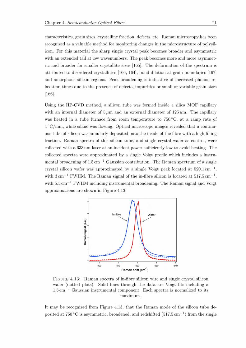
Chapter 4. Semiconductor Optical Fibres 71
characteristics, grain sizes, crystalline fraction, defects, etc. Raman microscopy has been
recognized as a valuable method for monitoring changes in the microstructure of polysil-
icon. For this material the sharp single crystal peak becomes broader and asymmetric
with an extended tail at low wavenumbers. The peak becomes more and more asymmet-
ric and broader for smaller crystallite sizes [165]. The deformation of the spectrum is
attributed to disordered crystallities [166, 164], bond dilation at grain boundaries [167]
and amorphous silicon regions. Peak broadening is indicative of increased phonon re-
laxation times due to the presence of defects, impurities or small or variable grain sizes
[166].
Using the HP-CVD method, a silicon tube was formed inside a silica MOF capillary
with an internal diameter of 5µm and an external diameter of 125µm. The capillary
was heated in a tube furnace from room temperature to 750 C, at a ramp rate of
4 C/min, while silane was flowing. Optical microscope images revealed that a continu-
ous tube of silicon was annularly deposited onto the inside of the fibre with a high filling
fraction. Raman spectra of this silicon tube, and single crystal wafer as control, were
collected with a 633 nm laser at an incident power sufficiently low to avoid heating. The
collected spectra were approximated by a single Voigt profile which includes a instru-
mental broadening of 1.5 cm−1 Gaussian contribution. The Raman spectrum of a single
crystal silicon wafer was approximated by a single Voigt peak located at 520.1 cm−1,
with 3 cm−1 FWHM. The Raman signal of the in-fibre silicon is located at 517.5 cm−1,
with 5.5 cm−1 FWHM including instrumental broadening. The Raman signal and Voigt
approximations are shown in Figure 4.13.
Figure 4.13: Raman spectra of in-fibre silicon wire and single crystal siliconwafer (dotted plots). Solid lines through the data are Voigt fits including a1.5 cm−1 Gaussian instrumental component. Each spectra is normalized to its
maximum.
It may be recognized from Figure 4.13, that the Raman mode of the silicon tube de-
posited at 750 C is asymmetric, broadened, and redshifted (517.5 cm−1) from the single

Chapter 4. Semiconductor Optical Fibres 72
crystal silicon (520.1 cm−1) peak. Asymmetry is given by the ratio of the half maximum
width on the low frequency side of the peak to the maximum width on the high fre-
quency side of the peak. Asymmetry is a characteristic of microcrystalline silicon due
to the presence of disordered crystallities and amorphous phases between grains.
Red-shifting of silicon Raman spectra can be due to both the effects of tensile strain
[168] and the presence of micro-nanocrystalline and/or amorphous material phases. To
separate the effects of strain on the Raman spectra, that might be present at the sil-
ica/silicon interface, from spectra broadening that is intrinsic to the microcrystalline
silicon sample itself, the silicon tubes were etched out of the silica fibre with HF acid.
A few hundred micrometres of the silica cladding were removed and micro-Raman spec-
trum was collected from both etched and unetched regions, which were close to each
other. A microscope image of an etched fibre is shown in Figure 4.14.
Figure 4.14: Microscope image of a silicon filled fibre partially etched from oneend. The silicon tube has been released from the silica MOF by HF etching; thescale bar is 5µm. The inset is a microscope image of the transverse deposition
profile before etching.
Micro-Raman spectra collected on the etched tube also exhibit an asymmetric peak,
but the peak center is now at 519.6 cm−1, indicating that removal of the tube from
the silica template has relieved strain (see Figure 4.15). This clearly confirms that
the red-shift observed for the in-fibre silicon tube is entirely due to strain induced at
the silica-silicon interface upon cooling from the annealing temperature of 750 C by
the difference in thermal expansion between the silicon tube and the silica fibre. The
transfer of shear stress is large enough to redshift the Raman mode by ∼ 2.5 cm−1 to the
silicon at this silica interface and indicates that the bonding between the two materials is
strong. The asymmetry and broadening of the Raman peak confirms the previous results
obtained with TEM which indicate that silicon tubes growth at 750 C are composed of
polycrystalline silicon with microcrystalline silicon, disordered micro/nano crystals and
amorphous material.
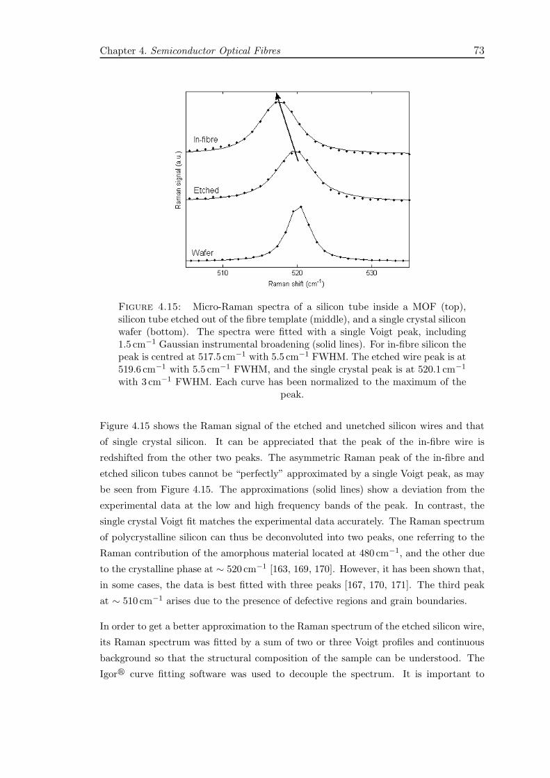
Chapter 4. Semiconductor Optical Fibres 73
Figure 4.15: Micro-Raman spectra of a silicon tube inside a MOF (top),silicon tube etched out of the fibre template (middle), and a single crystal siliconwafer (bottom). The spectra were fitted with a single Voigt peak, including1.5 cm−1 Gaussian instrumental broadening (solid lines). For in-fibre silicon thepeak is centred at 517.5 cm−1 with 5.5 cm−1 FWHM. The etched wire peak is at519.6 cm−1 with 5.5 cm−1 FWHM, and the single crystal peak is at 520.1 cm−1
with 3 cm−1 FWHM. Each curve has been normalized to the maximum of thepeak.
Figure 4.15 shows the Raman signal of the etched and unetched silicon wires and that
of single crystal silicon. It can be appreciated that the peak of the in-fibre wire is
redshifted from the other two peaks. The asymmetric Raman peak of the in-fibre and
etched silicon tubes cannot be “perfectly” approximated by a single Voigt peak, as may
be seen from Figure 4.15. The approximations (solid lines) show a deviation from the
experimental data at the low and high frequency bands of the peak. In contrast, the
single crystal Voigt fit matches the experimental data accurately. The Raman spectrum
of polycrystalline silicon can thus be deconvoluted into two peaks, one referring to the
Raman contribution of the amorphous material located at 480 cm−1, and the other due
to the crystalline phase at ∼ 520 cm−1 [163, 169, 170]. However, it has been shown that,
in some cases, the data is best fitted with three peaks [167, 170, 171]. The third peak
at ∼ 510 cm−1 arises due to the presence of defective regions and grain boundaries.
In order to get a better approximation to the Raman spectrum of the etched silicon wire,
its Raman spectrum was fitted by a sum of two or three Voigt profiles and continuous
background so that the structural composition of the sample can be understood. The
Igorr curve fitting software was used to decouple the spectrum. It is important to

Chapter 4. Semiconductor Optical Fibres 74
note that the peak fitting is very sensitive to the choice of starting parameters and the
conditions of the fitting procedure.
In the fitting process the amorphous contribution peak was fixed at 480 cm−1. The other
two peaks, attributed to micro/nanocrystals, grain boundaries and crystalline silicon
were left free to change in position, intensity, width and shape [172]. Then, several fits
were performed with different starting points; until a good approximation was obtained.
The coefficient r2 = 1− χ2 is a measure of the goodness of fit; an r2 of 1.0 is perfect fit
an r2 of 0.0 is complete lack of fit [173],
χ2 =SSE
SSM. (4.5)
SSE is the sum of squared residuals,
SSE =∑
i
(yi − yi)2 , (4.6)
where yi is the fitted value for a measured point yi. SSM is the deviation for yi from
the mean of the y data (y).
SSM =∑
i
(yi − y)2 , (4.7)
The fit obtained of the Raman spectra was only considered to be satisfactory when
r2 ≥ 0.99. When the Raman spectrum of the etched silicon wire was approximated
by a single Voigt peak the r2 = 0.97 value, whereas using two peaks (at 480 cm−1 and
∼ 520 cm−1) improved the value of the fitting procedure to r2 = 0.98. The use of three
peaks provided an excellent fit r2 = 0.99.
Figure 4.16 shows the results of the three peaks fitting procedure. The Raman spectrum
of the etched silicon wire is plotted in the figure and the inset shows a three Voigt peaks
approximation. The first peak is located at a 480 cm−1 with FWHM of ∼ 60 cm−1
attributed to amorphous silicon, the second peak at 517 cm−1 with a 11.1 cm−1 FWHM
attributed to boundary regions, defective silicon and small grain sizes. A third peak is
located at 519.6 cm−1 with a FWHM of 5.5 cm−1 due to crystallized grains of hundreds
of nanometres in diameter. The FWHM of the 519.6 cm−1 peak (5.5 cm−1) versus that
of the single crystal sample 3 cm−1, including instrumental broadening, together with
the presence of the two weaker peaks, is consistent with a mixed phase of silicon with
both amorphous and crystalline components of varying crystallite sizes [166].
The amorphous and microcrystalline portions of the sample will affect its electrical
and optical properties considerably. Voids and grain boundaries might contain a high
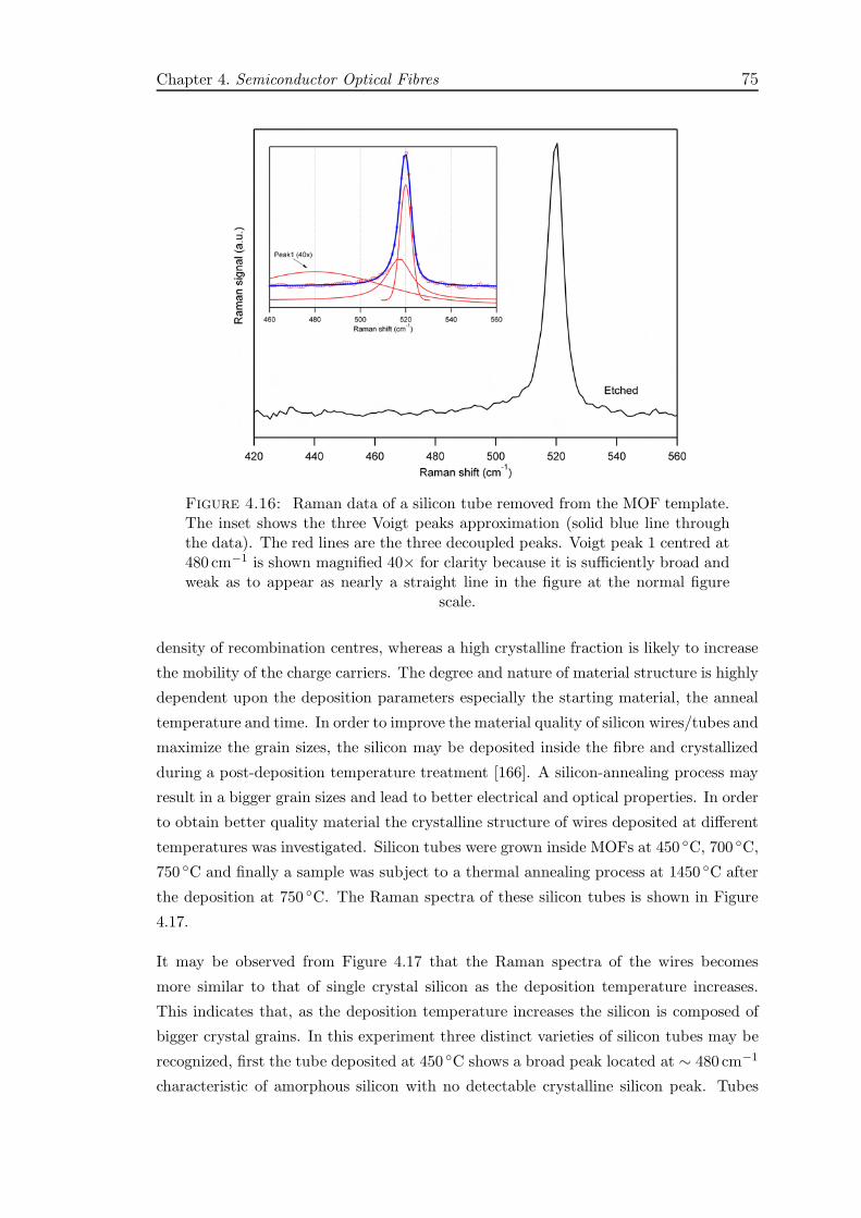
Chapter 4. Semiconductor Optical Fibres 75
Figure 4.16: Raman data of a silicon tube removed from the MOF template.The inset shows the three Voigt peaks approximation (solid blue line throughthe data). The red lines are the three decoupled peaks. Voigt peak 1 centred at480 cm−1 is shown magnified 40× for clarity because it is sufficiently broad andweak as to appear as nearly a straight line in the figure at the normal figure
scale.
density of recombination centres, whereas a high crystalline fraction is likely to increase
the mobility of the charge carriers. The degree and nature of material structure is highly
dependent upon the deposition parameters especially the starting material, the anneal
temperature and time. In order to improve the material quality of silicon wires/tubes and
maximize the grain sizes, the silicon may be deposited inside the fibre and crystallized
during a post-deposition temperature treatment [166]. A silicon-annealing process may
result in a bigger grain sizes and lead to better electrical and optical properties. In order
to obtain better quality material the crystalline structure of wires deposited at different
temperatures was investigated. Silicon tubes were grown inside MOFs at 450 C, 700 C,
750 C and finally a sample was subject to a thermal annealing process at 1450 C after
the deposition at 750 C. The Raman spectra of these silicon tubes is shown in Figure
4.17.
It may be observed from Figure 4.17 that the Raman spectra of the wires becomes
more similar to that of single crystal silicon as the deposition temperature increases.
This indicates that, as the deposition temperature increases the silicon is composed of
bigger crystal grains. In this experiment three distinct varieties of silicon tubes may be
recognized, first the tube deposited at 450 C shows a broad peak located at ∼ 480 cm−1
characteristic of amorphous silicon with no detectable crystalline silicon peak. Tubes
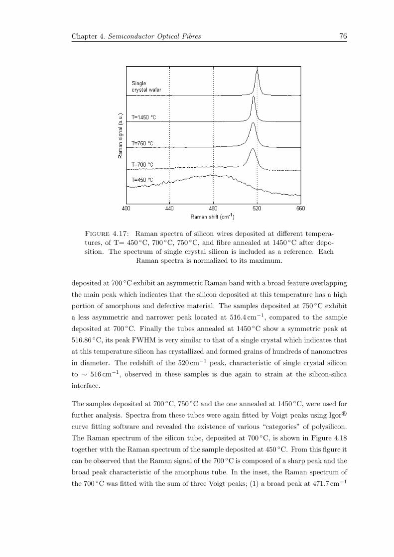
Chapter 4. Semiconductor Optical Fibres 76
Figure 4.17: Raman spectra of silicon wires deposited at different tempera-tures, of T= 450 C, 700 C, 750 C, and fibre annealed at 1450 C after depo-sition. The spectrum of single crystal silicon is included as a reference. Each
Raman spectra is normalized to its maximum.
deposited at 700 C exhibit an asymmetric Raman band with a broad feature overlapping
the main peak which indicates that the silicon deposited at this temperature has a high
portion of amorphous and defective material. The samples deposited at 750 C exhibit
a less asymmetric and narrower peak located at 516.4 cm−1, compared to the sample
deposited at 700 C. Finally the tubes annealed at 1450 C show a symmetric peak at
516.86 C, its peak FWHM is very similar to that of a single crystal which indicates that
at this temperature silicon has crystallized and formed grains of hundreds of nanometres
in diameter. The redshift of the 520 cm−1 peak, characteristic of single crystal silicon
to ∼ 516 cm−1, observed in these samples is due again to strain at the silicon-silica
interface.
The samples deposited at 700 C, 750 C and the one annealed at 1450 C, were used for
further analysis. Spectra from these tubes were again fitted by Voigt peaks using Igorr
curve fitting software and revealed the existence of various “categories” of polysilicon.
The Raman spectrum of the silicon tube, deposited at 700 C, is shown in Figure 4.18
together with the Raman spectrum of the sample deposited at 450 C. From this figure it
can be observed that the Raman signal of the 700 C is composed of a sharp peak and the
broad peak characteristic of the amorphous tube. In the inset, the Raman spectrum of
the 700 C was fitted with the sum of three Voigt peaks; (1) a broad peak at 471.7 cm−1
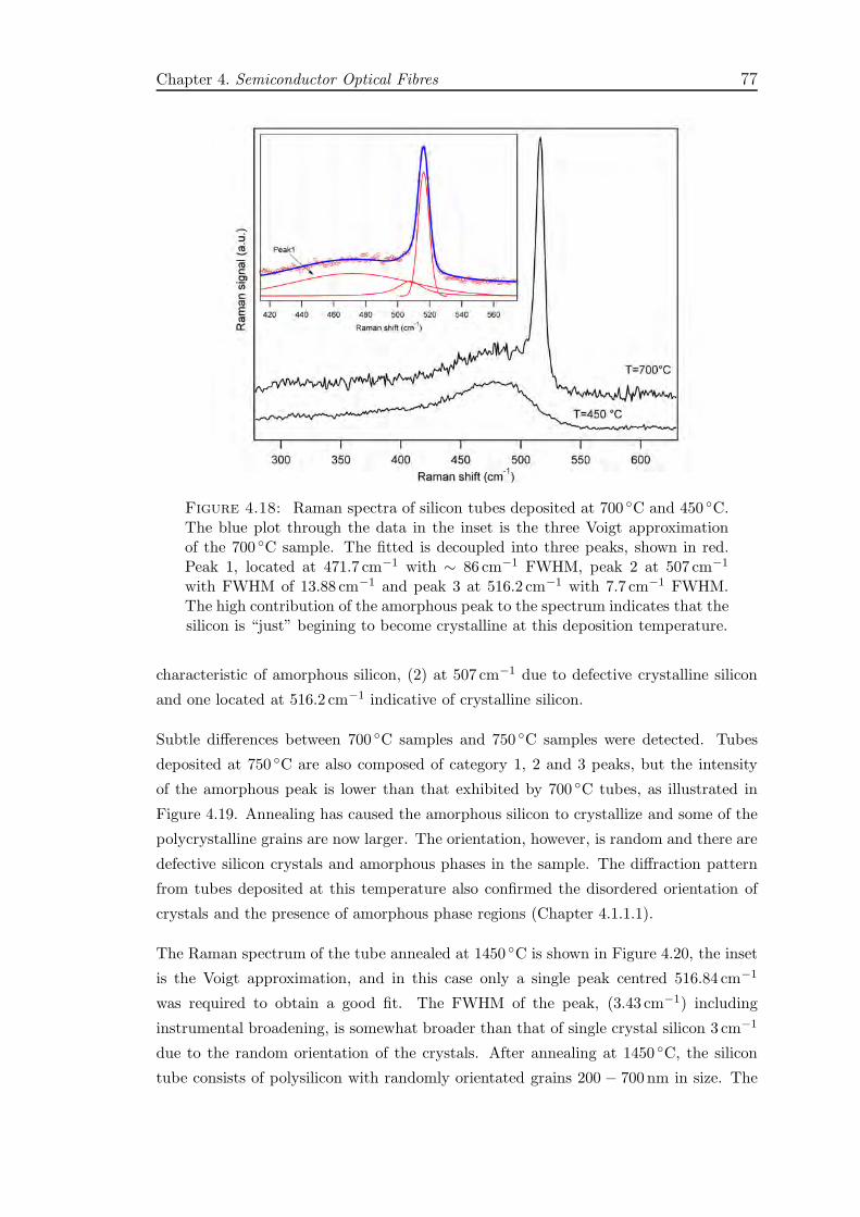
Chapter 4. Semiconductor Optical Fibres 77
Figure 4.18: Raman spectra of silicon tubes deposited at 700 C and 450 C.The blue plot through the data in the inset is the three Voigt approximationof the 700 C sample. The fitted is decoupled into three peaks, shown in red.Peak 1, located at 471.7 cm−1 with ∼ 86 cm−1 FWHM, peak 2 at 507 cm−1
with FWHM of 13.88 cm−1 and peak 3 at 516.2 cm−1 with 7.7 cm−1 FWHM.The high contribution of the amorphous peak to the spectrum indicates that thesilicon is “just” begining to become crystalline at this deposition temperature.
characteristic of amorphous silicon, (2) at 507 cm−1 due to defective crystalline silicon
and one located at 516.2 cm−1 indicative of crystalline silicon.
Subtle differences between 700 C samples and 750 C samples were detected. Tubes
deposited at 750 C are also composed of category 1, 2 and 3 peaks, but the intensity
of the amorphous peak is lower than that exhibited by 700 C tubes, as illustrated in
Figure 4.19. Annealing has caused the amorphous silicon to crystallize and some of the
polycrystalline grains are now larger. The orientation, however, is random and there are
defective silicon crystals and amorphous phases in the sample. The diffraction pattern
from tubes deposited at this temperature also confirmed the disordered orientation of
crystals and the presence of amorphous phase regions (Chapter 4.1.1.1).
The Raman spectrum of the tube annealed at 1450 C is shown in Figure 4.20, the inset
is the Voigt approximation, and in this case only a single peak centred 516.84 cm−1
was required to obtain a good fit. The FWHM of the peak, (3.43 cm−1) including
instrumental broadening, is somewhat broader than that of single crystal silicon 3 cm−1
due to the random orientation of the crystals. After annealing at 1450 C, the silicon
tube consists of polysilicon with randomly orientated grains 200 − 700 nm in size. The
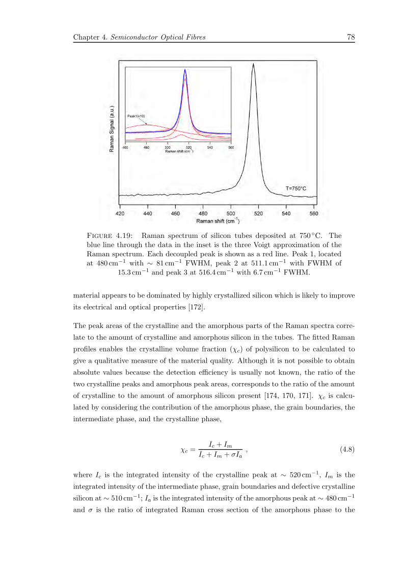
Chapter 4. Semiconductor Optical Fibres 78
Figure 4.19: Raman spectrum of silicon tubes deposited at 750 C. Theblue line through the data in the inset is the three Voigt approximation of theRaman spectrum. Each decoupled peak is shown as a red line. Peak 1, locatedat 480 cm−1 with ∼ 81 cm−1 FWHM, peak 2 at 511.1 cm−1 with FWHM of
15.3 cm−1 and peak 3 at 516.4 cm−1 with 6.7 cm−1 FWHM.
material appears to be dominated by highly crystallized silicon which is likely to improve
its electrical and optical properties [172].
The peak areas of the crystalline and the amorphous parts of the Raman spectra corre-
late to the amount of crystalline and amorphous silicon in the tubes. The fitted Raman
profiles enables the crystalline volume fraction (χc) of polysilicon to be calculated to
give a qualitative measure of the material quality. Although it is not possible to obtain
absolute values because the detection efficiency is usually not known, the ratio of the
two crystalline peaks and amorphous peak areas, corresponds to the ratio of the amount
of crystalline to the amount of amorphous silicon present [174, 170, 171]. χc is calcu-
lated by considering the contribution of the amorphous phase, the grain boundaries, the
intermediate phase, and the crystalline phase,
χc =Ic + Im
Ic + Im + σIa, (4.8)
where Ic is the integrated intensity of the crystalline peak at ∼ 520 cm−1, Im is the
integrated intensity of the intermediate phase, grain boundaries and defective crystalline
silicon at ∼ 510 cm−1; Ia is the integrated intensity of the amorphous peak at ∼ 480 cm−1
and σ is the ratio of integrated Raman cross section of the amorphous phase to the
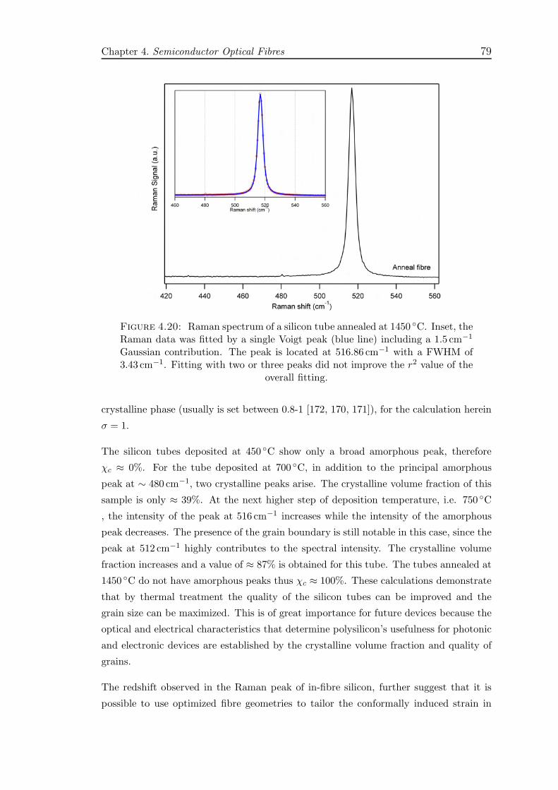
Chapter 4. Semiconductor Optical Fibres 79
Figure 4.20: Raman spectrum of a silicon tube annealed at 1450 C. Inset, theRaman data was fitted by a single Voigt peak (blue line) including a 1.5 cm−1
Gaussian contribution. The peak is located at 516.86 cm−1 with a FWHM of3.43 cm−1. Fitting with two or three peaks did not improve the r2 value of the
overall fitting.
crystalline phase (usually is set between 0.8-1 [172, 170, 171]), for the calculation herein
σ = 1.
The silicon tubes deposited at 450 C show only a broad amorphous peak, therefore
χc ≈ 0%. For the tube deposited at 700 C, in addition to the principal amorphous
peak at ∼ 480 cm−1, two crystalline peaks arise. The crystalline volume fraction of this
sample is only ≈ 39%. At the next higher step of deposition temperature, i.e. 750 C
, the intensity of the peak at 516 cm−1 increases while the intensity of the amorphous
peak decreases. The presence of the grain boundary is still notable in this case, since the
peak at 512 cm−1 highly contributes to the spectral intensity. The crystalline volume
fraction increases and a value of ≈ 87% is obtained for this tube. The tubes annealed at
1450 C do not have amorphous peaks thus χc ≈ 100%. These calculations demonstrate
that by thermal treatment the quality of the silicon tubes can be improved and the
grain size can be maximized. This is of great importance for future devices because the
optical and electrical characteristics that determine polysilicon’s usefulness for photonic
and electronic devices are established by the crystalline volume fraction and quality of
grains.
The redshift observed in the Raman peak of in-fibre silicon, further suggest that it is
possible to use optimized fibre geometries to tailor the conformally induced strain in

Chapter 4. Semiconductor Optical Fibres 80
silicon. Strain induced changes in silicon may lead to desirable changes in the elec-
tronic properties such as increased carrier mobility. Moreover, strain breaks silicon’s
centrosymmetric inversion symmetry and makes it an ideal electro-optic material [175].
4.1.2.2 Raman Spectroscopy of Germanium
Germanium tubes were also deposited inside 5µm silica capillaries. During the HP-
CVD, the capillaries were heated in a tube furnace from room temperature to 500 C,
at a ramp rate of 2 C/min, while a GeH4 precursor at 2MPa partial pressure in argon
carrier was flowing at a total pressure of 40MPa. The characteristic Raman spectra of
these tubes is show in Figure 4.21.
Figure 4.21: Micro-Raman spectrum of a germanium tube inside a fibre andthat of germanium single crystal wafer. Lines through the data are single Voigtfits including 1.5 cm−1 Gaussian component due to instrumental broadening.
Voigt fits, which included a 1.5 cm−1 Gaussian instrumental contribution, gave 3.31 cm−1
FWHM for the germanium wire in comparison to 3.1 cm−1 for single crystal germanium.
As in silicon, germanium Raman modes can be broadened by the presence of stress, mi-
crocrystalline or nanocrystalline grains, and/or amorphous phases. Amorphous and/or
nanocrystalline germanium phases typically exhibit Raman spectra at lower wavenum-
bers than bulk single crystal material. The germanium wire Raman spectra are sym-
metric and do not exhibit any low frequency tailing characteristic of the presence of
such phases. The somewhat broader (3.31 cm−1), but still symmetric, Raman mode
observed for the wire as compared with the wafer (3.1 cm−1) suggests that the sample
is crystalline, but not single crystalline. This was confirmed by transmission electron

Chapter 4. Semiconductor Optical Fibres 81
microscopy, TEM measurements, showed that there are microcrystalline, randomly ori-
ented, grains ∼ 500 nm in diameter (Chapter 4.1.1.2). There was little difference in the
position of the Raman modes for the wires in the fibre and the wafer, 299.8 cm−1 and
300.3 cm−1 respectively, indicating that there is little or no strain induced in the wires
upon cooling from the annealing temperature of 500 C.
4.2 Electrical Characterisation
A field effect transistor (FET) is a 3-terminal electronic device, configured like a parallel
plate capacitor with one of the electrodes replaced by a semiconductor. By control-
ling the voltage on one plate (gate), the distribution of charges in the semiconductor
are modified. These charges are injected from the source electrode and collected across
the semiconductor channel at the drain contact by applying a voltage between both
[176]. Figure 4.22 shows a schematic cross-section of a metal-oxide field effect transis-
tor(MOSFET), which are the most commonly used FETs in microelectronic circuits. If
the semiconductor between the source and the drain is n-type, a positive voltage applied
in the gate contact, leads to accumulation of electrons in the semiconductor (below the
gate) and enhances its conductivity. Conversely, Vgate < 0 depletes the holes in the
semiconductor and suppresses conductivity.
Figure 4.22: A schematic view of a FET. In this model electrons are injectedfrom the source and collected at the drain.
The current-voltage (I−V ) operation of a FET is typically displayed by plots of the drain
current Idrain as a function of the source-drain voltage Vsource, at fixed gate voltages Vgate
are called the output characteristic of the transistor. The Idrain vs. Vgate dependance for
a fixed Vsource are the transfer characteristics and show how efficiently the gate voltage
can switch the device “on” or “off”. Due to the FET’s digital nature, today there are
Chapter 4. Semiconductor Optical Fibres 82
millions of them in the processors used in personal computers, cellular phones, and many
other microelectronic devices.
Besides their numerous technological applications, FETs can be used to measure the
electronic transport of solid materials; this is because the device gives direct access to
the carrier type, concentration and mobility. To this end, germanium and silicon tubes
were deposited inside MOF capillaries with an internal diameter of 5µm. The deposition
temperature for the silicon tubes was 750 C and 500 C for germanium. The samples
were etched at both ends with HF acid to expose the semiconductor tube inside. These
were then mounted onto glass slides and masked off in the centre. The samples were
then evaporated with a 250 nm thick layer of aluminium, which is the classic ohmic
contact material for silicon and germanium. A contact is say to be ohmic when it has
been prepared so that the current-voltage characteristic of the contact is linear and
symmetric. After annealing at 435 C for 35min under an inert argon atmosphere, the
samples were finished off by removing the central mask [177]. This will reveal two
electrically isolated halves of the glass slide. The exposed ends of the capillaries were
covered with some Ga-In eutectic to form good electrical contacts with the sintered
aluminium on the etched ends of the fibre samples. These two end contacts become
the source and drain contacts, as in standard two-terminal I-V measurements. An
additional capacitatively coupled coaxial gate was also constructed by placing a drop of
the In-Ga eutectic onto a section of silica cladding ∼ 1mm in length in the middle of
the fibres. By applying a bias voltage to this contact, it was possible to apply a radial
electric field to the semiconductor core, thus using the silica cladding as a gate insulator
in a similar fashion to that seen in conventional FET devices.
The capacitance of the samples is determined using a simple co-axial approximation, with
the semiconductor core being treated as the central conductor and the silica cladding
being the cylindrical dielectric spacing between core and outer conductor (the eutec-
tic gate contact). The capacitance per unit length is therefore given by the standard
expression for co-axial capacitors [178]
C/L =2πǫε0
ln(h/r), (4.9)
where C is capacitance, L is the length of the gate (eutectic in the middle), ǫ is the
relative dielectric permittivity of the silica cladding, h is the cladding radius and r is
the radius of the semiconductor core. All of the electrical measurements were carried
out on a probe station using an Agilent 4155C semiconductor parameter analyzer. A
representation of the electric circuit is shown in Figure 4.23.
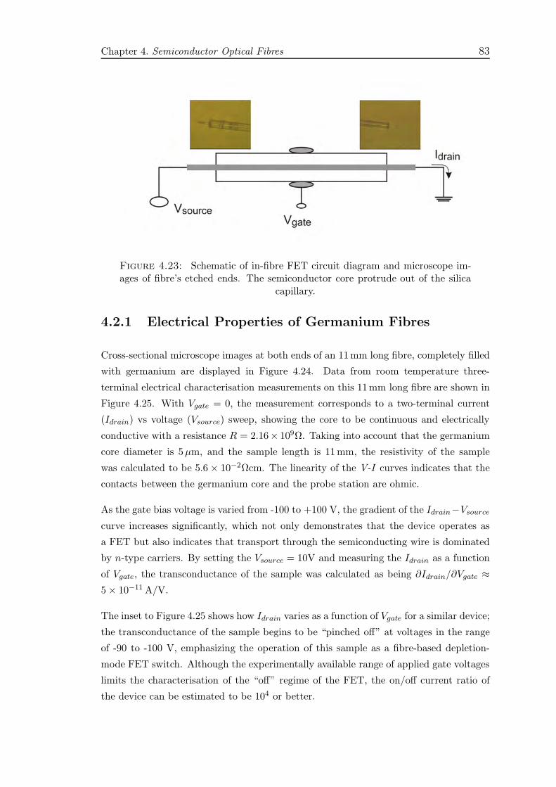
Chapter 4. Semiconductor Optical Fibres 83
Figure 4.23: Schematic of in-fibre FET circuit diagram and microscope im-ages of fibre’s etched ends. The semiconductor core protrude out of the silica
capillary.
4.2.1 Electrical Properties of Germanium Fibres
Cross-sectional microscope images at both ends of an 11mm long fibre, completely filled
with germanium are displayed in Figure 4.24. Data from room temperature three-
terminal electrical characterisation measurements on this 11mm long fibre are shown in
Figure 4.25. With Vgate = 0, the measurement corresponds to a two-terminal current
(Idrain) vs voltage (Vsource) sweep, showing the core to be continuous and electrically
conductive with a resistance R = 2.16× 10⁹Ω. Taking into account that the germanium
core diameter is 5µm, and the sample length is 11mm, the resistivity of the sample
was calculated to be 5.6 × 10⁻²Ωcm. The linearity of the V-I curves indicates that the
contacts between the germanium core and the probe station are ohmic.
As the gate bias voltage is varied from -100 to +100 V, the gradient of the Idrain−Vsource
curve increases significantly, which not only demonstrates that the device operates as
a FET but also indicates that transport through the semiconducting wire is dominated
by n-type carriers. By setting the Vsource = 10V and measuring the Idrain as a function
of Vgate, the transconductance of the sample was calculated as being ∂Idrain/∂Vgate ≈5 × 10⁻¹¹ A/V.
The inset to Figure 4.25 shows how Idrain varies as a function of Vgate for a similar device;
the transconductance of the sample begins to be “pinched off” at voltages in the range
of -90 to -100 V, emphasizing the operation of this sample as a fibre-based depletion-
mode FET switch. Although the experimentally available range of applied gate voltages
limits the characterisation of the “off” regime of the FET, the on/off current ratio of
the device can be estimated to be 104 or better.
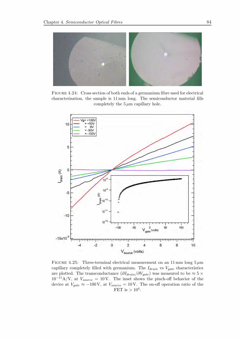
Chapter 4. Semiconductor Optical Fibres 84
Figure 4.24: Cross section of both ends of a germanium fibre used for electricalcharacterisation, the sample is 11mm long. The semiconductor material fills
completely the 5µm capillary hole.
Figure 4.25: Three-terminal electrical measurement on an 11mm long 5µmcapillary completely filled with germanium. The Idrain vs Vgate characteristicsare plotted. The transconductance (∂Idrain/∂Vgate) was measured to be ≈ 5 ×10⁻¹¹A/V, at Vsource = 10V. The inset shows the pinch-off behavior of thedevice at Vgate ≈ −100V, at Vsource = 10V. The on-off operation ratio of the
FET is > 104.

Chapter 4. Semiconductor Optical Fibres 85
By interpolating the linear slope of ∂Idrain/∂Vgate for a given Vsource, the majority carrier
mobility may also be estimated from the three-terminal data, depending on the sample
capacitance and the length of the gate contact according to the equation [178, 179]
∂Idrain
∂Vgate= µ ·
(
C
L2
)
Vsource (4.10)
The silica dielectric cladding used in equation (4.9) to calculate the capacitance for the
germanium sample was 94µm in diameter and 1.5mm long, resulting in a capacitance
per unit length of ∼ 6 × 10⁻¹¹Fm−1. Using equation (4.10), the calculated device mo-
bility is 1.05 cm2/Vs at room temperature, as compared with typical room temperature
electron mobilities of 100 cm2/Vs in bulk polycrystalline germanium devices [180]. As
mobility is defined as the velocity with which charge carriers move under the application
of an electric field, the low mobility measured in our samples clearly reflects the fact
that charge transport occurs with high scattering of carriers at impurity sites, grain
boundaries and lattice dislocations.
By considering the gate voltage at which “pinch-off”, and hence depletion of the ma-
terial occurs, it was possible to estimate the carrier concentration in these n-type Ge-
fibre FETs. The electron carrier density was estimated from the total charge Qtot =
CVpinch−off required to deplete the FET. The concentration of free carriers may be
calculated by using the following equation [178, 181]
n =CVpinch−off
e · Lπr2 , (4.11)
where e is the electron charge. Considering that the “pinch-off” occurs at Vgate ≈−100V, the free carrier concentration is calculated to be n = 2.1 × 1015 cm−3 for this
Ge-fibre FET.
4.2.2 Electrical Properties of Silicon Fibres
A 5µm silicon filled fibre capillary, with cladding thickness of 125µm and sample length
of 18mm was electrically characterised. The capillary hole was partially filled with sili-
con, forming a smooth silicon tube with a filling fraction of ∼ 50%, as illustrated in Fig-
ure 4.26. Figure 4.27 shows a set of typical current vs source-drain voltage data obtained
from a silicon-fibre FET at different gate voltages. The two-terminal Idrain − Vsource
curves are all linear, thus indicating that the metal electrodes make ohmic contacts to
the silicon tube. The gate-dependence of the Idrain − Vsource curves again indicate that
the majority of the carriers are again n-type, with a sample resistivity of 0.21Ωcm and
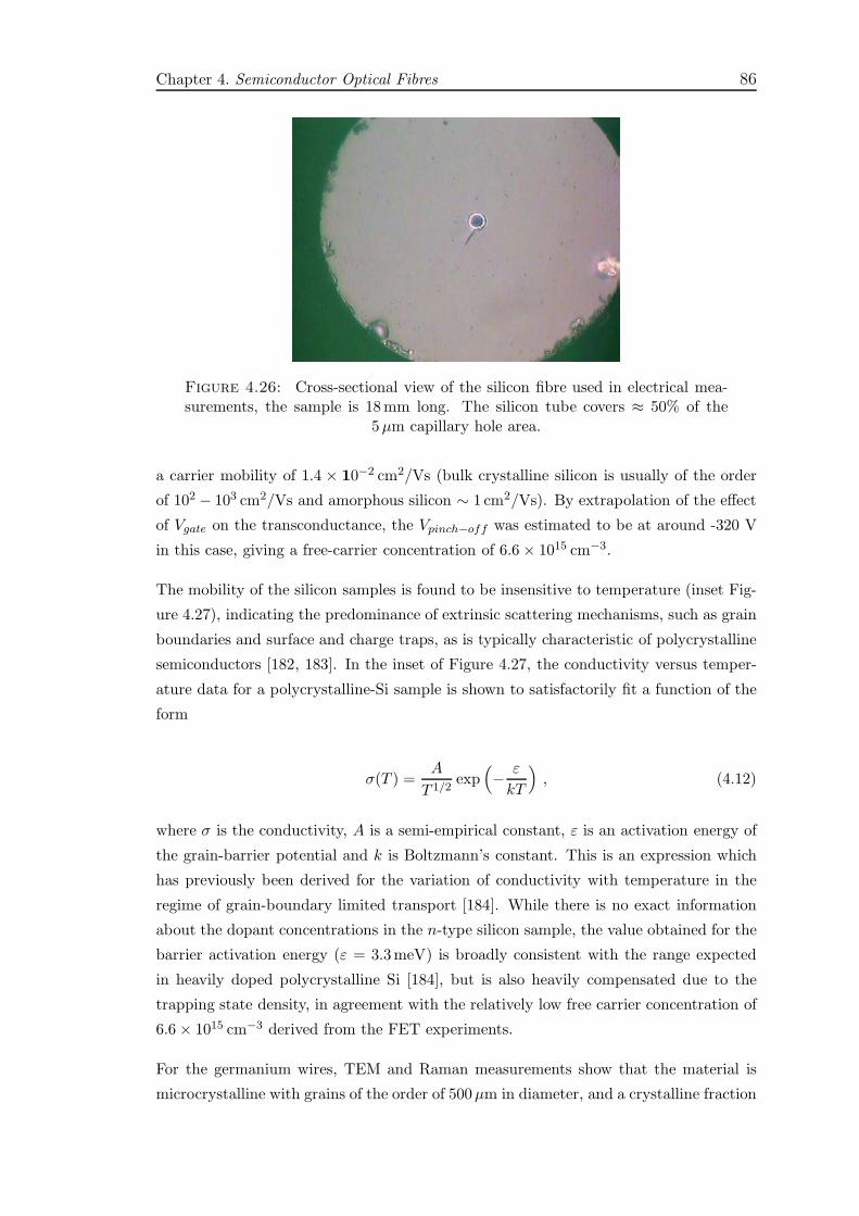
Chapter 4. Semiconductor Optical Fibres 86
Figure 4.26: Cross-sectional view of the silicon fibre used in electrical mea-surements, the sample is 18mm long. The silicon tube covers ≈ 50% of the
5µm capillary hole area.
a carrier mobility of 1.4 × 10⁻² cm2/Vs (bulk crystalline silicon is usually of the order
of 102 − 103 cm2/Vs and amorphous silicon ∼ 1 cm2/Vs). By extrapolation of the effect
of Vgate on the transconductance, the Vpinch−off was estimated to be at around -320 V
in this case, giving a free-carrier concentration of 6.6 × 1015 cm−3.
The mobility of the silicon samples is found to be insensitive to temperature (inset Fig-
ure 4.27), indicating the predominance of extrinsic scattering mechanisms, such as grain
boundaries and surface and charge traps, as is typically characteristic of polycrystalline
semiconductors [182, 183]. In the inset of Figure 4.27, the conductivity versus temper-
ature data for a polycrystalline-Si sample is shown to satisfactorily fit a function of the
form
σ(T ) =A
T 1/2exp
(
− ε
kT
)
, (4.12)
where σ is the conductivity, A is a semi-empirical constant, ε is an activation energy of
the grain-barrier potential and k is Boltzmann’s constant. This is an expression which
has previously been derived for the variation of conductivity with temperature in the
regime of grain-boundary limited transport [184]. While there is no exact information
about the dopant concentrations in the n-type silicon sample, the value obtained for the
barrier activation energy (ε = 3.3meV) is broadly consistent with the range expected
in heavily doped polycrystalline Si [184], but is also heavily compensated due to the
trapping state density, in agreement with the relatively low free carrier concentration of
6.6 × 1015 cm−3 derived from the FET experiments.
For the germanium wires, TEM and Raman measurements show that the material is
microcrystalline with grains of the order of 500µm in diameter, and a crystalline fraction

Chapter 4. Semiconductor Optical Fibres 87
Figure 4.27: Three-terminal electrical measurement on a 18mm length ofa 5µm Si-filled capillary. The Idrain vs Vsource characteristics are plotted fordifferent Vgate values. The transconductance (∂Idrain/∂Vgate) was determinedas being ≈ 1 × 10⁻¹²A/V, with Vsource = 20V. The inset shows how theconductivity (+) and mobility (N) values of such a fibre change as a functionof temperature. The conductivity data is also fitted by a technique of leastsquares to equation (4.12) (red line through the data). This approximation
yields a value of 3.3meV for the grain-barrier activation energy (ε).
χc ≈ 100%. The electrical properties reflect the high quality of the polycrystalline
semiconductor. In contrast, for the silicon wires deposited at 750 C, the Raman data
indicates a crystallinity of χc ∼ 87%. TEM data indicate the presence of a distribution
of grain sizes, including nanocrystalline and amorphous materials. Thus, the silicon
wires exhibit a mobility about three orders of magnitude less than typical for device
quality polycrystalline silicon [185]. However, the germanium wires have a mobility
only about two orders of magnitude less than polycrystalline germanium. This one
order of magnitude difference in the ratio sample/reference between the materials can be
attributed to the differences in the grain structure between silicon and germanium, which
can be annealed for grain growth at significantly lower temperatures than for silicon. The
present results indicate that reducing the magnitude of the grain-boundary scattering
within semiconductor tubes encased in optical fibres is key to further improvements
Chapter 4. Semiconductor Optical Fibres 88
in electronic transport properties. Annealing of silicon wires at higher temperatures
and optimization of the time-temperature ramps used for such annealing, as well as
the amount of strain, should allow for a reduction of the amount of amorphous and
nanocrystalline silicon along with giving an enhanced grain growth and thus fewer grain
boundaries. The Raman signal of silicon wires, annealed at 1450 C, indicates that χc ≈100% and that no amorphous material was detected, therefore the electrical properties
of wires annealed at this temperature are expected to be higher than those shown by
the silicon samples presented in this section. Future experiments will be focused on the
electrical characterisation of silicon in-fibre wire/tubes annealed at 1450C.
Finally, it is worth mentioning that this is the first time that operation of FETs or
any other electronic device has been demonstrated within optical fibres filled with crys-
talline semiconductors. This suggest that the high pressure CVD technique provides an
attractive platform for the development of a wide array of next generation, fibre-based
optoelectronics.
4.3 Optical Characterisation of Silicon MOFs
During the last decades, silicon photonics has created great interest with research groups
all over the world. The high transparency and high nonlinearity of silicon at commu-
nications wavelengths, combined with the well-developed silicon top-down processing
techniques, renders, silicon as an excellent material for photonic device miniaturization
and the future generation of optoelectronic integrated circuits.
Silicon-on-insulator (SOI) waveguides consists of a single crystal silicon layer separated
from the silicon substrate by SiO2. The silica layer provides the low index cladding and
light is confined to travel in the high refractive index silicon layer. SOI compared with
other integrated optics platforms provides tight optical confinement, due to the large
refractive index of silicon which minimizes radiation leakage into the silica substrate.
SOI has become as promising platform material and has led to several reports of in-
tegrated waveguides [186, 187, 188], beam splitters, add-drop filter, attenuators [189].
Although passive devices with high performance have been fabricated in SOI, adding
optical functionality to a silicon chip is one of the most challenging problems of materials
research. Silicon is a centro-symmetric material and so second order nonlinear effects
in silicon are negligible. Consequently, the need for active devices, such as modulators
and switches, has motivated researchers to explore other mechanisms to induce refrac-
tive index change in silicon [98]. In the last few years thermo-optic effects [190] and
free carrier injection have been used to demonstrate high performance modulators and
switches [191, 192, 193]. Recently, strain on silicon planar waveguides was used to break

Chapter 4. Semiconductor Optical Fibres 89
the crystal symmetry so that significant electro-optic effect could be induced [175] and
an optical modulator was demonstrated.
In addition, a major limitation of this material for optoelectronic applications is that
silicon is an indirect bandgap semiconductor, which makes it an inefficient emitter of
light. Many different effects have been investigated to overcome this limitation and, only
recently, stimulated Raman scattering has emerged as the most promising mechanism
for achieving in-chip lasing from silicon [194, 195, 196]. Both devices, silicon modulators
and lasers, have opened up new promising opportunities for silicon photonics.
Although single crystal silicon has lower optical loss (∼ 1 dB/cm) and better electrical
properties than polycrystalline and amorphous silicon, these phases can be useful for
certain devices. The main reason for this is their ease of deposition which allows flexibil-
ity in the design and multilevels of interconnection. They also offer the possibility of a
wider range of cladding and core thicknesses on a variety of substrates and cheaper pro-
cessing cost as compared to single crystal devices. In 1996, Agarwal et al. [197] reported
on the fabrication of a poly-Si waveguide with optical loss of 16 dB/cm. Later on, by
improving the surface morphology and decreasing bulk absorption, the same research
group reported a further reduction in the bulk loss of poly-Si material to 9 dB/cm [198].
More recently, the Intel silicon photonics group reported on the fabrication of a fast
all-silicon optical modulator in which the active material was poly-Si [192]. The 6.7 dB
on-chip loss of their device was mainly attributed to the doped poly-silicon phase shifter
and undoped poly-Si waveguide.
4.3.1 Silicon Optical Fibres
The impregnation of poly-silicon within MOFs voids offers new possibilities with silicon
photonics. Devices such as in-fibre silicon modulators, short fibre Raman lasers and
optical switches may be envisaged.
Figure 4.28: Microscope image of a 2µm capillary fibre filled with silicon.This fibre was used in optical experiments. The cladding diameter is 125µm.
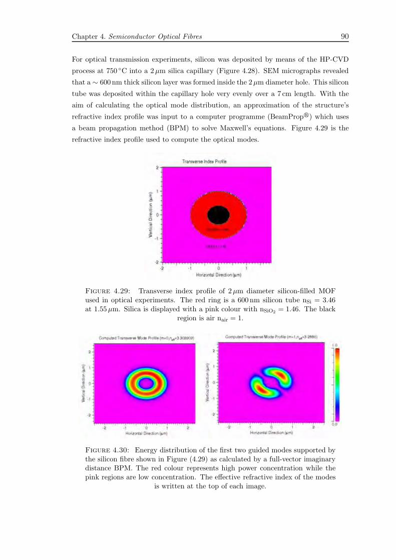
Chapter 4. Semiconductor Optical Fibres 90
For optical transmission experiments, silicon was deposited by means of the HP-CVD
process at 750 C into a 2µm silica capillary (Figure 4.28). SEM micrographs revealed
that a ∼ 600 nm thick silicon layer was formed inside the 2µm diameter hole. This silicon
tube was deposited within the capillary hole very evenly over a 7 cm length. With the
aim of calculating the optical mode distribution, an approximation of the structure’s
refractive index profile was input to a computer programme (BeamPropr) which uses
a beam propagation method (BPM) to solve Maxwell’s equations. Figure 4.29 is the
refractive index profile used to compute the optical modes.
Figure 4.29: Transverse index profile of 2µm diameter silicon-filled MOFused in optical experiments. The red ring is a 600 nm silicon tube nSi = 3.46at 1.55µm. Silica is displayed with a pink colour with nSiO2
= 1.46. The blackregion is air nair = 1.
Figure 4.30: Energy distribution of the first two guided modes supported bythe silicon fibre shown in Figure (4.29) as calculated by a full-vector imaginarydistance BPM. The red colour represents high power concentration while thepink regions are low concentration. The effective refractive index of the modes
is written at the top of each image.

Chapter 4. Semiconductor Optical Fibres 91
Figure 4.30 shows the first two guided modes supported by the structure, as calculated
with BPM. The simulations indicate that this fibre is highly multimode and 15 degen-
erate modes are allowed to propagate in the silicon core. In contrast to conventional
silica fibres, in this fibre the electromagnetic fields are tightly concentrated in the small
silicon ring, as expected for the high refractive index contrast between silicon and silica
∆n ≈ 2.
A high power continuous wave (CW) laser diode was used to launch up to 100mW
of λ = 1.55µm radiation into the fibre core. A 0.65 numerical aperture (NA) 3.1mm
focal length IR aspheric lens was used to focus the beam waist onto the core. The
fibre alignment was controlled using xyz nanometer precision stages with piezo-electric
actuators. The coupled light was guided by a 5 cm silicon fibre whose end faces were
mechanically cleaved. The output near-field was collimated with a 40× objective and
focused onto a Electrophysics IR vidicon camera, in order to image the mode profile. For
transmission measurements the output power was collected by a germanium photodiode
attached to a Newport 2832C power meter and compared to the input power which was
monitored simultaneously.
Figure 4.31: Near field image of the transmitted light through the 2µm siliconMOF.
Due to the short fibre length and small core dimensions, it was not possible to entirely
decouple the light in the cladding from that transmitted in the core, even though index
matching fluid was applied. Other problems encountered during optical characterisation
experiments included the low coupling efficiency, caused by the high Fresnel reflection
at the air-silicon interfaces (R ≈ 30%) and small core. Figure 4.31 is the near-field
output of the transmitted mode, obtained with an IR camera. It can be appreciated
that the laser radiation has been confined into the silicon core but a lot energy remains
in the cladding. Although this experiment clearly indicated that light was guided by
the silicon core, it was very convenient to remove the cladding light to do reliable loss
measurement and to verify the structure’s guiding properties. Approximately 2mm of
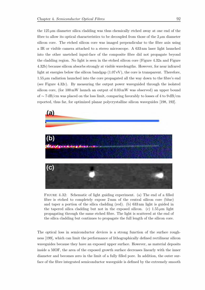
Chapter 4. Semiconductor Optical Fibres 92
the 125µm diameter silica cladding was thus chemically etched away at one end of the
fibre to allow its optical characteristics to be decoupled from those of the 2µm diameter
silicon core. The etched silicon core was imaged perpendicular to the fibre axis using
a IR or visible camera attached to a stereo microscope. A 633 nm laser light launched
into the other unetched input-face of the composite fibre did not propagate beyond
the cladding region. No light is seen in the etched silicon core (Figure 4.32a and Figure
4.32b) because silicon absorbs strongly at visible wavelengths. However, for near infrared
light at energies below the silicon bandgap (1.07 eV), the core is transparent. Therefore,
1.55µm radiation launched into the core propagated all the way down to the fibre’s end
(see Figure 4.32c). By measuring the output power waveguided through the isolated
silicon core, (for 100mW launch an output of 0.03mW was observed) an upper bound
of ∼ 7 dB/cm was placed on the loss limit, comparing favorably to losses of 4 to 9 dB/cm
reported, thus far, for optimized planar polycrystalline silicon waveguides [198, 192].
Figure 4.32: Schematic of light guiding experiment. (a) The end of a filledfibre is etched to completely expose 2mm of the central silicon core (blue)and taper a portion of the silica cladding (red). (b) 633 nm light is guided inthe tapered silica cladding but not in the exposed silicon. (c) 1.55µm lightpropagating through the same etched fibre. The light is scattered at the end ofthe silica cladding but continues to propagate the full length of the silicon core.
The optical loss in semiconductor devices is a strong function of the surface rough-
ness [199], which can limit the performance of lithographically defined rectilinear silicon
waveguides because they have an exposed upper surface. However, as material deposits
inside a MOF, the area of the exposed growth surface decreases linearly with the inner
diameter and becomes zero in the limit of a fully filled pore. In addition, the outer sur-
face of the fibre integrated semiconductor waveguide is defined by the extremely smooth
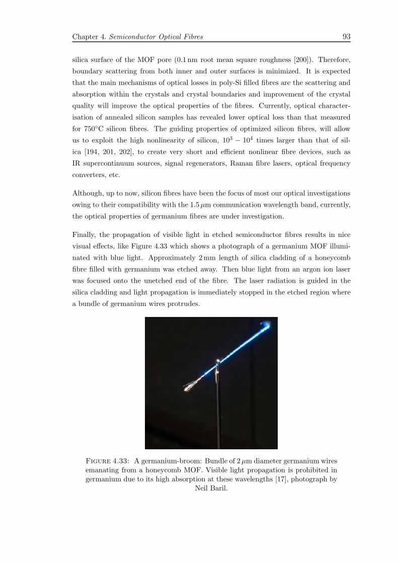
Chapter 4. Semiconductor Optical Fibres 93
silica surface of the MOF pore (0.1 nm root mean square roughness [200]). Therefore,
boundary scattering from both inner and outer surfaces is minimized. It is expected
that the main mechanisms of optical losses in poly-Si filled fibres are the scattering and
absorption within the crystals and crystal boundaries and improvement of the crystal
quality will improve the optical properties of the fibres. Currently, optical character-
isation of annealed silicon samples has revealed lower optical loss than that measured
for 750C silicon fibres. The guiding properties of optimized silicon fibres, will allow
us to exploit the high nonlinearity of silicon, 103 − 104 times larger than that of sil-
ica [194, 201, 202], to create very short and efficient nonlinear fibre devices, such as
IR supercontinuum sources, signal regenerators, Raman fibre lasers, optical frequency
converters, etc.
Although, up to now, silicon fibres have been the focus of most our optical investigations
owing to their compatibility with the 1.5µm communication wavelength band, currently,
the optical properties of germanium fibres are under investigation.
Finally, the propagation of visible light in etched semiconductor fibres results in nice
visual effects, like Figure 4.33 which shows a photograph of a germanium MOF illumi-
nated with blue light. Approximately 2mm length of silica cladding of a honeycomb
fibre filled with germanium was etched away. Then blue light from an argon ion laser
was focused onto the unetched end of the fibre. The laser radiation is guided in the
silica cladding and light propagation is immediately stopped in the etched region where
a bundle of germanium wires protrudes.
Figure 4.33: A germanium-broom: Bundle of 2µm diameter germanium wiresemanating from a honeycomb MOF. Visible light propagation is prohibited ingermanium due to its high absorption at these wavelengths [17], photograph by
Neil Baril.

Chapter 4. Semiconductor Optical Fibres 94
4.3.2 In-Fibre Silicon Modulator
As was mentioned before, i.e. the free carrier plasma dispersion effect, the change of
refractive index and absorption caused by the concentration variation of free carriers
has been used widely in planar silicon modulators and active devices. As a proof of
principle, Don-Jin Won a member of the group in PSU has carried out light modulation
experiments on amorphous silicon-filled MOFs. Although, the author of this thesis has
not directly participated in these experiments the first optical measurements of these
fibres were done in Southampton and have been the basis for future experiments.
Despite the fact that amorphous silicon contains more point defects than crystalline sil-
icon and the optical absorption in amorphous silicon can be substantial, these point de-
fects can be passivated to some extent by the incorporation of hydrogen. Hydrogenated
a:Si has shown good electrical properties and low optical absorption [203]. Hydrogenated
amorphous silicon wires were fabricated inside a 6µm diameter silica capillary by the
HP-CVD method, using 5% silane diluted in the mixture of 10% hydrogen and 85%
helium at a total gas pressure of 38MPa. The MOFs were then heated at 480 C in a
tube furnace to induce thermal decomposition of silane, while the gas precursor flowed
through the fibre. The initial hole was completely filled with hydrogenated amorphous
silicon over several centimetres of length [204].
The change of refractive index and absorption caused by the concentration variation of
free carriers in semiconductors may be used to modulate the intensity of guided light
in the silicon core. The density change of carriers modifies the transmission loss due
to free carrier absorption [98]. This effect can be induced by either carrier-injection
with p-n junctions [205, 192] or photo excitation by light [206]. The a:Si fibre was
used as an all-optical modulator of guided 1.55µm laser radiation using the free-carrier
plasma-dispersion effect generated by a 514 nm pump laser in the silicon core [204]. The
schematic diagram of the optical in-fibre modulator is shown in Figure 4.34. In the
experiments 20mW of CW laser radiation at 1.55µm is coupled into the core using free
space optics. The transmitted light is focused into a collection fibre which is connected
to an ultrafast photodetector. Nanosecond pulses from a Nd:YAG laser are doubled
in frequency to generate 532 nm pulses of ∼ 17.5 ns at 10Hz repetition rate. In order
to excite electron and hole pairs into the extended states of a:Si, the pump pulses are
laterally focused onto the silicon core using a cylindrical lens [204].
When free carriers are generated the refractive index and the loss of the silicon core
increases. The change in the amplitude of the detected signal allows us to identify the
intensity modulation depth M which reflects the optical bistability, defined by

Chapter 4. Semiconductor Optical Fibres 95
Figure 4.34: Schematic diagram of an all-optical in-fibre light modulator.The probe signal at 1.55µm is guided by the fibre’s a:Si core. The pump pulsesexcite free carriers that change the optical properties of the silicon core, and
modulate the amplitude of the probe signal (from reference [204])
M =Imax − Imin
Imax, (4.13)
where Imin and Imax are the power of the probe signal during photoexcitation and
ground states, respectively. For pulses of 65µJ the M value was measured to be as high
as 85%. This prototype a:Si MOF modulator is a major step towards high-speed in-fibre
devices. With the successful synthesis of devices like this one, based on semiconductor
fibres, the opportunities of replacing planar optoelectronics with more compatible in-
fibre semiconductor devices will enter a new era.

Chapter 5
Optical Properties of Metal
Nanoparticles
The previous chapter has described the characterisation of semiconductor-modified mi-
crostructured optical fibres. SEM, TEM and micro-Raman analysis was used to study
the material properties of these fibres. Silicon and germanium in-fibre wires were con-
figured as FET to determine the material conductivity and carrier mobility. Finally,
semiconductor-fibres were used as IR optical waveguides and by the photo-excitation
of free carriers light modulation was achieved. This chapter is an introduction to the
field of plasmonics and provides a theoretical background to Chapter 6 which describes
Surface-Enhanced Raman Scattering, and to Chapter 7 where the optical and SERS
characterisation of metal-modified microstructured optical fibres is presented.
5.1 Introduction
Metals have played an important role in the development of modern civilisation and have
formed the subject of one of the most ancient themes of scientific research. Nowadays,
they are the main materials used for guiding electromagnetic radiation at microwave
frequencies but, due to their high conductivity in the optical regime, they show strong
absorption in the visible and infrared wavelengths which has limited their extension as
optical waveguides. However, the optical properties of metals change when their struc-
tural dimensions are smaller than the wavelength of light. Nanoscale metallic structures
have led to an exponentially increasing number of applications in the context of emerging
plasmonics and nanosciences.
96

Chapter 5. Optical Properties of Metal Nanoparticles 97
Evidence suggest that colloidal metals may have appeared as early as 5th century B.C.
in Egypt, and since then they have fascinated people and especially scientists because of
their intense and brilliant colours. One of the most famous examples of exploiting the
optical properties of metal nanoparticles in ancient times is the Lycurgus Cup, that was
manufactured by the Romans. The cup is ruby in transmitted light but green in reflected
light due to the presence of silver and gold nanoparticles (see Figure 5.1). During the
Middle Ages, gold and silver nanoparticles were again used as a pigment of stained glass
windows in Medieval churches.
The interest in understanding the optical properties of metal nanoparticles dates back
to Faraday’s experiments [207]. In these experiments, Faraday noticed the remarkable
dependence of the colour of gold nanoparticles on their size. Also he observed reversible
colour changes of thin films prepared from dried colloidal solutions of gold upon me-
chanical compression.
Figure 5.1: Lycurgus glass cup, demonstrating the bright red and greencolours, in transmitted and reflected light of gold nanoparticles. Inset: scanningelectron microscopy (SEM) image of a characteristic nanocrystal embedded in
the cup’s glass, from the British Museum website [208].
The optical characteristics of colloidal gold and silver are due to the interaction between
the conduction electrons and light. When light interacts with conduction electrons
that are confined in a very small volume they can perform a collective oscillation with
respect to the positive-ion nuclei, creating a negative charge distribution at the surface.
This electron oscillation is therefore called a surface plasmon. The excitation of surface
plasmon resonances is what produces a very selective absorption and strong scattering
of light.
In order to tailor the next generation of micro/nano metallo-dielectric devices and ma-
terials, novel ways to organize the nanoparticles into controlled architectures must be
found. This chapter will explore the optical properties of metals and focus on a method
Chapter 5. Optical Properties of Metal Nanoparticles 98
to organize nanoparticles in microstructured optical fibres to exploit their plasmonic
properties.
5.2 Classical Optics of Metals
The propagation of electromagnetic waves in a metal may be described by considering a
metal as a homogeneous isotropic medium having a high conductivity (σ). With these
considerations Maxwell’s equations can be written as follows
∇× ~E = −µ∂~H
∂t, (5.1a)
∇× ~H = εm∂ ~E
∂t+ σ ~E , (5.1b)
∇ · ~H = 0 , (5.1c)
∇ · ~E = 0 . (5.1d)
Equation (5.1d) represents the fact that free charges are absent in the interior of an ho-
mogeneous metal. This can be easily demonstrated by taking the divergence of equation
(5.1b), which then takes the form
ε∇ · ∂~E
∂t+ σ∇ · ~E = 0 . (5.2)
Substituting ∇ · ~E = ρ in the previous equation,
∂ρ
∂t+σ
ερ = 0 . (5.3)
Solving this equation by integration yields,
ρ = ρ0 exp(−t/τ) , (5.4)
where τ = (εm/σ). Thus the charge density ρ in a medium is seen to fall exponentially
with time. The relaxation time τ ≃ 10−18 s is exceedingly small for metals that have
an appreciable conductivity. In addition, this time is much shorter than the period of
an optical wave and so an electrostatic equilibrium is established faster than a variation
of the field. Consequently, for a highly conductive medium it is appropriate to say that
ρ = 0 [209, 210] and, thus, ∇ · ~E = 0.

Chapter 5. Optical Properties of Metal Nanoparticles 99
The system of equations (5.1) determines the propagation of electromagnetic waves in
a conducting material. To explore the propagation of electromagnetic waves, again, one
can introduce an electric field of the form ~E = ~E0 expi(~k · z − ωt). This represents a
monochromatic plane wave and is a solution of the following wave equation,
2 ~E = µ
(
ε+ iσ
ω
) ∂2 ~E
∂t2. (5.5)
If a complex dielectric function is defined as ε′ = εm + i(σ/ω) = ε1 + iε2, the equation
above can easily be reduced to the wave equation of a transparent material
2 ~E + k2 ~E = 0 , (5.6)
where k2 = ω2µε′ = ω2µ(
ε+ iσω
)
. Likewise, a complex refractive index may be defined
as, n′ =√
ε′/ε0 =√ǫ1 + iǫ2, n
′ = n+ iκ,
n =
√
√
ǫ21 + ǫ22 + ǫ12
and κ =
√
√
ǫ21 + ǫ22 − ǫ12
, (5.7)
where n is the refractive index and κ is the absorption coefficient. The wavevector k can
now be written as k = (ω/c)(n + jκ) so that the electric field becomes
~E = ~E0 eiω( zn
c−t)e−zω(κ
c ) . (5.8)
So far in this and in the previous chapters, the dielectric properties of a matter have
been considered as constants but, in practice, matter cannot respond immediately to
an excitation field. The optical response of a material results from its interaction with
the electromagnetic wave within some characteristic time. This temporal response leads
to a time dependence of the dielectric permittivity of materials, and therefore on the
frequency (dispersion) of the incident electric field. In order to understand the dispersion
of the medium it is necessary to carry out a microscopic analysis of the interaction
between light and the atomic structure of the material. Fortunately, it is possible to
make a simplified model of the atom by considering a fixed heavy particle (the nucleus)
surrounded by light particles (electrons) which can move around the central nucleus. A
convenient way of discussing the dispersion relations of metals is to divide their electronic
structure in two classes, bound and free electrons.

Chapter 5. Optical Properties of Metal Nanoparticles 100
5.3 Optical Response of Bound Electrons (Lorentz
Model)
In a dielectric material the electrons are bound to the atomic nuclei by quasi-elastic forces
and when an electromagnetic wave interacts with the bound electrons they oscillate and
generate a periodic dipole moment. The Lorentz model describes the behavior of the
electrons joined to the atomic nuclei by quasi-elastic forces. Movement of bound electron
by an electromagnetic field of a linearly polarised wave is described by
md2r
dt2+mγ
dr
dt+ Cr = −eE0exp(−iωt) , (5.9)
where e and m are the charge and mass of the electron, respectively. C is a spring
constant describing restoring forces due to electrostatic attraction. Since the dielectric
dipole moment of the system is dependent on the distance r between the nuclei and the
vibrating electrons, the oscillating electrons will emit electromagnetic waves which carry
energy away (scattering). Therefore, a damping constant, (γ), must be introduced into
the motion equation to describe losses due to scattering and other dissipation mech-
anisms (e.g. because of collisions between the atoms). Solving the Lorentz equation
5.9 and considering the relations between the dielectric dipole moment (~p = −e~r), the
polarisability of the medium (~P = Nb~p) and its dielectric properties, it can be shown
that the permittivity of a dielectric follows the next relations
ǫ1 = 1 +ω2
p(ω20 − ω2)
(ω20 − ω2)2 + γ2ω2
and ǫ2 =ω2
pγω
(ω20 − ω2)2 + γ2ω2
, (5.10)
where ω0 =√
Cm is the natural frequency of the electron oscillations and ωp =
√
Nbe2
mε0is
known as the plasma frequency and Nb is the density of bound electrons. The previous
equations, know as Lorentz relations, describe the dispersion and absorption for bound
electrons (Figure 5.2).
5.4 Optical Response of Free Electrons (Drude
Model)
In the case of a perfect conductive medium the electrons are free to move between the
molecules and are said to be free electrons. Metals are know as free-electron metals
if most of their optical and electronic properties are due to their conduction electrons
Chapter 5. Optical Properties of Metal Nanoparticles 101
[211]. The optical properties of metals can be explained by assuming the existence of
an electron gas moving between the positive ions which form the crystal lattice of the
metal and can be well described by the Drude model [212]. This model assumes a gas
of independent electrons that can freely move with a common average relaxation time
τ . The drift-motion of free electrons due to an external electric field ~E = ~E0exp(−iωt)
can be obtained by solving the following equation
md2r
dt2+mγ
dr
dt= −eE0exp(−iωt) , (5.11)
where the coefficient γ = 1/τ is the electron relaxation rate which is a phenomenologi-
cal damping coefficient that quantifies the dissipation of energy due to electron-photon
interactions, collisions of the electron gas with the lattice ions, lattice defects and impu-
rities.
The current density J(ω) = −Nfedrdt and the conductivity of a metal can be obtained
by solving the equation (5.11),
J(ω) =Nfe
2
m
E(ω)
( 1τ − iω)
and σ(ω) =σ0
(1 − iωτ), (5.12)
where σ0 =Nf e2τ
m . Using the previous result in equation (5.5), the dielectric function
ǫ(ω) = ǫ1(ω)+iǫ2(ω) of a system with Nf free electrons per unit volume, may be written
as
ǫ1 = 1 −ω2
p
ω2 + γ2and ǫ2 =
ω2pγ
ω(ω2 + γ2)(5.13)
for highly conductive metals at visible frequencies, ω2vis ≫ γ2, the dielectric function can
be approximated to
ǫ1 = 1 −ω2
p
ω2and ǫ2 = i
ω2pγ
ω3(5.14)
where ωp =√
Nfe2
mε0is the plasma frequency. Figure(5.2) shows the real and imaginary
parts of the dielectric constants of a free-electron metal calculated with equation (5.14).
In Figure 5.2 one can identify three regions with different optical properties. First an
absorbing region which extends from zero to ω ∼ γ, light in this window is highly
absorbed. Secondly, a reflective region corresponding to a metallic reflection. At a
certain frequency ω = ωp, the dielectric function is equal to zero and the electron

Chapter 5. Optical Properties of Metal Nanoparticles 102
0
ω
Die
lect
ric P
erm
ittiv
ity
Dielectric (Lorentz model)
0
Ref
ract
ive
Inde
x
ωo
ε2
n
κ
ε1
ωp
ωo
ωp
ω
0
0
Dei
lect
ric P
erm
ittiv
ity
Metal (Drude Model)
0
0
Ref
ract
ive
inde
x
ε2
n
κ
ε1
ωp
ωp ω
ωγ
γ
Figure 5.2: Plots of the dielectric function of a dielectric (left) and a free-electron metal (right) calculated using the Lorentz relations (5.10) and Druderelations (5.14), respectively. The complex refractive index was obtained using
equation (5.7).
density fluctuation is longitudinal. At this frequency it is possible to consider all the
oscillating electrons as a single entity known as a volume plasmon. For most metals the
plasma frequency is in the UV, however, as will be described in the following sections,
the plasmon frequency in a metal can be shifted to the visible range when the material
is structured. The last frequency region ω > ωp corresponds to the transparent regime.
Because the electrons cannot respond fast enough to screen the electric field for high
frequencies, metals are transparent to light.
Some alkaline metals, like sodium, have nearly free-electron behavior and their optical
properties are well described by Drude’s model [213]. However, for metals like silver or
gold the electrons in deeper levels contribute to their dielectric function and Drude’s
theory fails to accurately describe their properties, especially at visible frequencies.
5.5 Real Metals
Noble metal atoms like Cu, Ag or Au have completely filled 3d, 4d, and 5d shells and
just one electron in the 4s, 5s, and 6s bands, respectively. The d-band electrons are
very close to the Fermi level and interband transitions between occupied bands into
conduction band can be excited by photons with energies corresponding to visible and
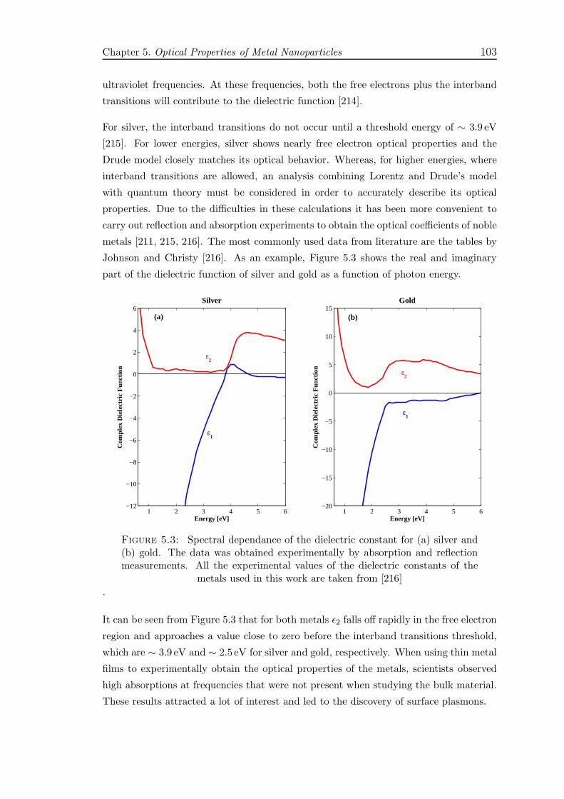
Chapter 5. Optical Properties of Metal Nanoparticles 103
ultraviolet frequencies. At these frequencies, both the free electrons plus the interband
transitions will contribute to the dielectric function [214].
For silver, the interband transitions do not occur until a threshold energy of ∼ 3.9 eV
[215]. For lower energies, silver shows nearly free electron optical properties and the
Drude model closely matches its optical behavior. Whereas, for higher energies, where
interband transitions are allowed, an analysis combining Lorentz and Drude’s model
with quantum theory must be considered in order to accurately describe its optical
properties. Due to the difficulties in these calculations it has been more convenient to
carry out reflection and absorption experiments to obtain the optical coefficients of noble
metals [211, 215, 216]. The most commonly used data from literature are the tables by
Johnson and Christy [216]. As an example, Figure 5.3 shows the real and imaginary
part of the dielectric function of silver and gold as a function of photon energy.
1 2 3 4 5 6−12
−10
−8
−6
−4
−2
0
2
4
6
Energy [eV]
Com
plex
Die
lect
ric
Fun
ctio
n
Silver
ε2
ε1
(a)
1 2 3 4 5 6−20
−15
−10
−5
0
5
10
15
Energy [eV]
Com
plex
Die
lect
ric
Fun
ctio
n
Gold
ε2
ε1
(b)
Figure 5.3: Spectral dependance of the dielectric constant for (a) silver and(b) gold. The data was obtained experimentally by absorption and reflectionmeasurements. All the experimental values of the dielectric constants of the
metals used in this work are taken from [216]
.
It can be seen from Figure 5.3 that for both metals ǫ2 falls off rapidly in the free electron
region and approaches a value close to zero before the interband transitions threshold,
which are ∼ 3.9 eV and ∼ 2.5 eV for silver and gold, respectively. When using thin metal
films to experimentally obtain the optical properties of the metals, scientists observed
high absorptions at frequencies that were not present when studying the bulk material.
These results attracted a lot of interest and led to the discovery of surface plasmons.
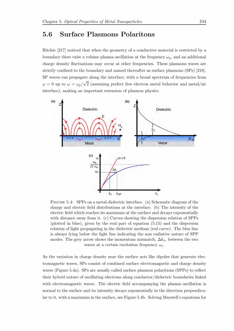
Chapter 5. Optical Properties of Metal Nanoparticles 104
5.6 Surface Plasmons Polaritons
Ritchie [217] noticed that when the geometry of a conductive material is restricted by a
boundary there exist a volume plasma oscillation at the frequency ωp, and an additional
charge density fluctuations may occur at other frequencies. These plasmons waves are
strictly confined to the boundary and named thereafter as surface plasmons (SPs) [218].
SP waves can propagate along the interface, with a broad spectrum of frequencies from
ω = 0 up to ω = ωp/√
2 (assuming perfect free electron metal behavior and metal/air
interface), making an important extension of plasmon physics.
Figure 5.4: SPPs on a metal-dielectric interface. (a) Schematic diagram of thecharge and electric field distributions at the interface. (b) The intensity of theelectric field which reaches its maximum at the surface and decays exponentiallywith distance away from it. (c) Curves showing the dispersion relation of SPPs(plotted in blue), given by the real part of equation (5.15) and the dispersionrelation of light propagating in the dielectric medium (red curve). The blue lineis always lying below the light line indicating the non radiative nature of SPPmodes. The grey arrow shows the momentum mismatch, ∆kx, between the two
waves at a certain excitation frequency ωe.
As the variation in charge density near the surface acts like dipoles that generate elec-
tromagnetic waves, SPs consist of combined surface electromagnetic and charge density
waves (Figure 5.4a). SPs are usually called surface plasmon polaritions (SPPs) to reflect
their hybrid nature of oscillating electrons along conductor/dielectric boundaries linked
with electromagnetic waves. The electric field accompanying the plasma oscillation is
normal to the surface and its intensity decays exponentially in the direction perpendicu-
lar to it, with a maximum in the surface, see Figure 5.4b. Solving Maxwell’s equations for

Chapter 5. Optical Properties of Metal Nanoparticles 105
electromagnetic waves with frequency ω, propagating along a metal/dielectric interface,
shows that only TM modes can exist and yields the dispersion relation
k′SP = k0
√
ǫdǫ′mǫd + ǫ′m
, (5.15)
where k′SP = kSP1 + ikSP2 is the complex propagation constant of the SPPs in the
direction parallel to the interface, ǫ′m and ǫd are the frequency-dependent permittivity
of the metal and the dielectric material respectively. The real and imaginary part of
k′SP are
kSP1 = k0
√
ǫdǫm1
ǫd + ǫm1and kSP2 = k0
(
ǫdǫm1
ǫd + ǫm1
)3/2 ǫm2
2ǫ2m1
. (5.16)
The dispersion relation of SPP, plotted in Figure 5.4c, shows that their momentum ~kSP1
is greater than that of a free-space photon of the same frequency ~k0. This increase in
momentum is linked with the binding of the electromagnetic wave to the surface and
describes the non-radiative nature of SPP.
In contrast to the propagating nature of the SPP along the surface, the electric field
Ez decays exponentially into both media, preventing energy propagation away from the
surface. In the dielectric medium its decay length is of the order of half the wavelength
of light, whereas the penetration distance into the metal is determined by the skin depth.
Figure 5.4c, shows that for low frequency plasmons their properties closely match those
of an electromagnetic wave indicating that the field concentrates most of its energy in the
dielectric medium. Additionally, this figure shows a resonant effect when the plasmon
frequency approaches ωp/√
1 + ǫd. Near the resonance, large wavevector SPPs exhibit
a greater concentration of the field at the interface. Their energy becomes independent
of the wavevector and their properties closely resemble those of a volume plasmon.
When light is incident upon a planar metal surface, it cannot be directly transformed
into SPP since the wavevector parallel to the surface of the SPP is greater than that
of the incident radiation. If light is to be converted into SPP, at a certain photon
frequency ω, its wave vector ~k0 has to be increased by a value of ∆kx, as illustrated
in Figure 5.4c. There are three main techniques by which the missing momentum can
be provided. The first one makes use of periodic dielectric structures, with period Λ.
In this configuration the light wavevector is increased by integer values of the lattice
vector G = 2π/Λ. The periodic media couples light waves for which ∆kx = m~G and
strong coupling between the incident light and the SPP may occur when the wave vector
condition ksp1 = k||air±mG = k0 sin θ±mG is satisfied (see Figure 5.5a). This technique
has been an important means for the study of SPPs [219, 220, 221, 222, 223].
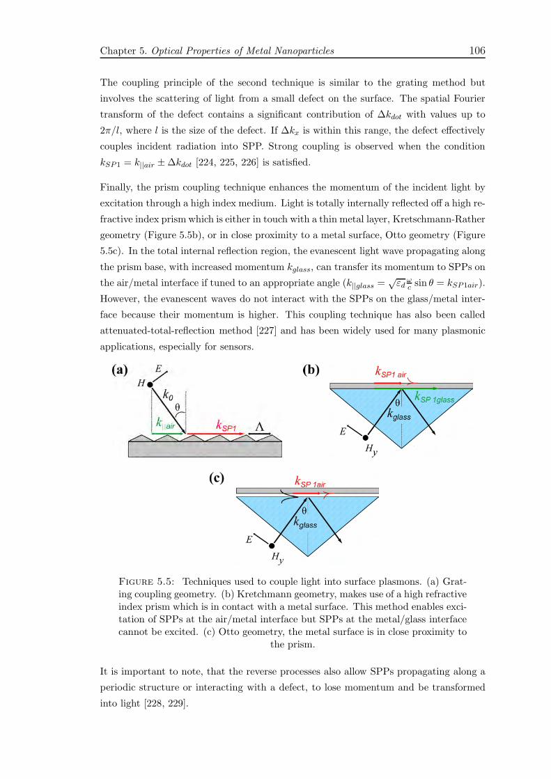
Chapter 5. Optical Properties of Metal Nanoparticles 106
The coupling principle of the second technique is similar to the grating method but
involves the scattering of light from a small defect on the surface. The spatial Fourier
transform of the defect contains a significant contribution of ∆kdot with values up to
2π/l, where l is the size of the defect. If ∆kx is within this range, the defect effectively
couples incident radiation into SPP. Strong coupling is observed when the condition
kSP1 = k||air ± ∆kdot [224, 225, 226] is satisfied.
Finally, the prism coupling technique enhances the momentum of the incident light by
excitation through a high index medium. Light is totally internally reflected off a high re-
fractive index prism which is either in touch with a thin metal layer, Kretschmann-Rather
geometry (Figure 5.5b), or in close proximity to a metal surface, Otto geometry (Figure
5.5c). In the total internal reflection region, the evanescent light wave propagating along
the prism base, with increased momentum kglass, can transfer its momentum to SPPs on
the air/metal interface if tuned to an appropriate angle (k||glass =√εd
ωc sin θ = kSP1air).
However, the evanescent waves do not interact with the SPPs on the glass/metal inter-
face because their momentum is higher. This coupling technique has also been called
attenuated-total-reflection method [227] and has been widely used for many plasmonic
applications, especially for sensors.
Figure 5.5: Techniques used to couple light into surface plasmons. (a) Grat-ing coupling geometry. (b) Kretchmann geometry, makes use of a high refractiveindex prism which is in contact with a metal surface. This method enables exci-tation of SPPs at the air/metal interface but SPPs at the metal/glass interfacecannot be excited. (c) Otto geometry, the metal surface is in close proximity to
the prism.
It is important to note, that the reverse processes also allow SPPs propagating along a
periodic structure or interacting with a defect, to lose momentum and be transformed
into light [228, 229].
Chapter 5. Optical Properties of Metal Nanoparticles 107
The imaginary part of the SPP’s wave vector, kSP2 in equation (5.16), corresponds to
ohmic loss in the metal. The SPP field intensity decays exponentially during propa-
gation along the surface, its propagation distance, δSP = 1/2kSP2, is of the order of
micrometres at visible frequencies, increasing to millimetres in the near-infrared region.
Although the short propagation distance of SPP has been a major limitation to con-
sider plasmonic/photonic components, recently SPP devices shorter than δSP , have been
demonstrated [230, 231, 232].
5.7 Localized Surface Plasmons
In addition to SPP on a plane surface, in other geometries involving major spatial
confinement, such as metallic nanoparticles, localized surface plasmons (LSP) can be
excited. As it is characteristic of a enclosed system, SPPs will propagate within the
metal particle and the reflected wave will interfere with itself leading to standing charge
density waves. LSP resonances are present at discrete frequencies which depend on the
size and shape of the object to which the plasmon is confined [233]. In contrast to volume
plasmons and SPP which have a single resonant frequency, 3D confined structures have
an infinite number of plasmon resonances of different symmetry. If the size of the system
L is small compared with the wavelength of light L ≪ λ, the standing wave will follow
the time dependence of the incident light, and the particles will take a dipole form, as
illustrated in Figure 5.6. With an increase in the particle size (L ∼ λ) higher symmetry
modes (multipoles resonances) become more important. The resonance conditions of a
small metal particle are given by
ǫm1(ω) = −ǫd(
l + 1
l
)
, (5.17)
where l = 1, 2, 3 . . . . Except for the first resonance l = 1, which is dipolar, the others
have symmetries corresponding to higher multipoles and therefore are non-radiative
[234]. The dipole resonance can be excited with incident light of the resonant frequencies,
independent of the wavevector.
The numerical basis for describing the absorption, scattering properties of spherical
metal particles are again the Maxwell equations. The Mie-Lorentz theory provides
solutions for the scattering of a plane wave by an isotropic sphere-ellipsoid embedded in
a homogeneous medium. In this formulation, the incident plane wave and the scattering
field are expanded into spherical Bessel and Hankel functions. The internal field is also
expanded into spherical functions. By enforcing the boundary condition on the particle
surface, the electromagnetic field inside and outside the particle can be computed [212].
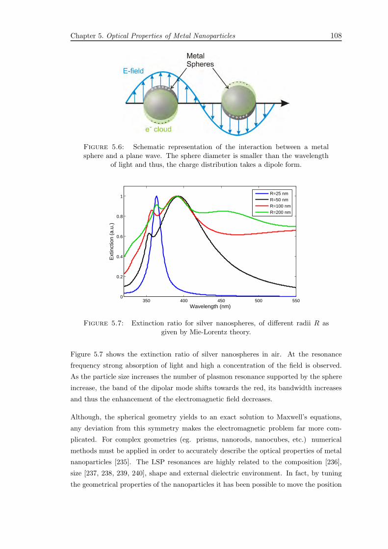
Chapter 5. Optical Properties of Metal Nanoparticles 108
Figure 5.6: Schematic representation of the interaction between a metalsphere and a plane wave. The sphere diameter is smaller than the wavelength
of light and thus, the charge distribution takes a dipole form.
350 400 450 500 5500
0.2
0.4
0.6
0.8
1
Wavelength (nm)
Ext
inct
ion
(a.u
.)
R=25 nmR=50 nmR=100 nmR=200 nm
Figure 5.7: Extinction ratio for silver nanospheres, of different radii R asgiven by Mie-Lorentz theory.
Figure 5.7 shows the extinction ratio of silver nanospheres in air. At the resonance
frequency strong absorption of light and high a concentration of the field is observed.
As the particle size increases the number of plasmon resonance supported by the sphere
increase, the band of the dipolar mode shifts towards the red, its bandwidth increases
and thus the enhancement of the electromagnetic field decreases.
Although, the spherical geometry yields to an exact solution to Maxwell’s equations,
any deviation from this symmetry makes the electromagnetic problem far more com-
plicated. For complex geometries (eg. prisms, nanorods, nanocubes, etc.) numerical
methods must be applied in order to accurately describe the optical properties of metal
nanoparticles [235]. The LSP resonances are highly related to the composition [236],
size [237, 238, 239, 240], shape and external dielectric environment. In fact, by tuning
the geometrical properties of the nanoparticles it has been possible to move the position

Chapter 5. Optical Properties of Metal Nanoparticles 109
of the LSP resonance across the visible and near-IR spectra [241, 242]. The unique tun-
ability of metallic nanoparticles offer the opportunity of placing the plasmon resonances
at a desired wavelength for a particular application, as it is shown in Figure 5.8.
Figure 5.8: Solution of metallic nanoshells, as the shell thickness is increasedthe plasmon resonance is tunned from the visible to infrared wavelengths, taken
from reference [243]
5.8 Plasmonic Devices and Applications
The topic of surface plasmons polaritons has a history going back more than a hun-
dred years, but it has recently attracted renewed interest for a variety of reasons. In
part, this is because there are now well developed nanoscale fabrication techniques such
as electron-beam lithography, ion-beam milling, and self assembly that allow suitable
metal/dielectric structures to be fabricated as a way of controlling SPPs. Another moti-
vation for their study is because the field of plasmonics has great potential in a number
of fundamental physics and practical applications. Plasmon devices find widespread use
in present day commercial industries and in different areas of science and technology.
For example, they have been used as bio-molecular sensors, for the characterisation of
the optical properties of matter, and they show good prospects for the development of
subwavelength lithography techniques and optics. This section describes some of the
work that has been done in the field of plasmonics with practical applications.
5.8.1 Sensors and Biosensors
Sensing is probably the most attractive and widely studied application of plasmon waves
and a great deal of work has been done in the exploitation of SPPs for biochemical
sensing. When in resonance, plasmon structures serve as a local probe of the dielectric
medium within a few nanometres of the metal boundary. The enhanced evanescent field
near the metal structure allows for a variety of sensing applications and techniques.
There are two main types of plasmon sensors. The first one is based on the excitation of
Chapter 5. Optical Properties of Metal Nanoparticles 110
SPPs waves in thin metal films and the second relies on the excitation of LSPs in metal
nanostructures.
SPPs sensors have been used since the late seventies and the early eighties saw the
first demonstration of gas and biomolecule detection systems [244] based on plasmon-
mater interactions. Because the resonance frequency of the plasmon waves depends
on the refractive index of the dielectric environment (equation (5.15)), any changes in
the optical properties of the region close to the metal boundary modifies the resonance
frequency of the SPPs and can be detected with simple devices. SPPs in thin metal-
lic films sensors are excited by prisms or grating coupling mechanisms. The shift in
the resonant frequency due to the surrounding environment manifests as a shift in the
angle of maximum optical absorption [245]. The sensitivity of the SPP resonance to
its immediate environment offers great opportunities to characterise thin metallic films,
detect molecules attached to the surface, study biomolecular bounding, environmental
changes, etc. For example, by functionalising a metal film by antibodies, specific for
single or multiple antigens, and by monitoring the shift of the resonant frequency upon
interaction of the binding molecules, it is possible to measure the rates of reactions,
the strength of biomolecular binding and the concentration of antigens [246]. The SPR
sensor technology has been commercialized by several companies [246, 247, 248] and
has become the main label-free technology for the study of real-time biomolecular inter-
actions. As the resonance frequency of LSPs in metal nanostructures depends notably
on the refractive index of its immediate environment, metal nanostructures have also
been used for sensing applications [249, 250, 251]. However, because of the difficulties
in the production of reproducible structures it has not been so widely used as its planar
counterpart.
The second kind of plasmon sensors are based on the enhancement of spectroscopy
techniques due localized surface plasmon resonance. These sensors take advantage of the
fact that LSPs are radiative and provide even higher field enhancements than SPPs (on
smooth surfaces) due to the strong three dimensional localization of the electromagnetic
fields. Therefore, the matter-light interactions and optical nonlinear effects associated
with the environment in close proximity to the surface can be studied with low light
intensities. It has been demonstrated that LSPs can greatly amplify the signal of several
optical spectroscopy techniques. LSPs are the basis of powerful phenomena such as
Surface Enhanced Fluorescence Spectroscopy [252, 253, 254], Surface Enhanced Infrared
Absorption Spectroscopy [255, 256] and Surface Enhanced Raman Scattering (SERS)
[234, 257, 258] to mention a few. In SERS the molecules attached to the surface of
metal nanostructures interact with the high field intensity of LSPs and induce enhanced
Raman photons. SERS has recently received great interest, and reports of new and more
stable SERS substrates can constantly be found in scientific literature as well as being

Chapter 5. Optical Properties of Metal Nanoparticles 111
used in commercial devices [259, 260]. The SERS effect is discussed in the following
chapter and the development of novel SERS substrates based on the deposition of silver
nanoparticles within microstructured optical fibres is described in Chapter 7.
Figure 5.9: (a) Commercially available plasmon sensors. Top: biosensor basedon SPP resonances in smooth gold films, taken from reference [247]. Bottom:the high localization of EM fields at the surface of nanostructured metal filmhas been exploited for Surface Enhanced Raman Scattering sensing, from ref-erence [260]. (b) Top: SEM image of silver nanostructure used for enhancedtransmission experiments. Bottom: Image of transmitted light, from reference[261]. (c) Top: SEM micrograph of a subwavelength plasmonic Mach-Zehnderinterferometer. Bottom: Near field image of the propagating plasmon waves.
Taken from reference [262].
5.8.2 Extraordinary Optical Transmission
In 1998 Ebbesen and co-workers [263] reported that the intensity of light transmitted
through a metal film with an array of subwavelength apertures is much higher than
expected. High transmission of light through nanoholes promises exciting opportunities
for subwavelength optical lithography using conventional photoresist and UV lasers [261,
264] leading to great interest in the microelectronics and optoelectronics industries. It
is believed that the structuring of the metal surface excites SPPs waves that can travel
around the holes and, when both SPPs waves on each side of the film are in phase, the
resonant transmission occurs. However, the explanation of this phenomenon in terms of
SPPs has been questioned and many theories involving diffraction and near field optics
can be found in the literature [265, 266].
Chapter 5. Optical Properties of Metal Nanoparticles 112
5.8.3 Photonic Integration
The areas of computing and communications have boosted a tremendous progress in
the development of faster and smaller microelectronic components and during the last
few decades we have seen a tremendous miniaturization of electronic circuits. However,
electronic devices based on CMOS technology are approaching their limits both in the
level of integration and the operational frequency. Quantum effect devices such as single
electron transistors, quantum well and quantum dot structures have been considered as a
possible approach in computer design. Another alternative is developing all-optical pro-
cessing devices where the information is processed and transfered in the form of photons.
In recent years there has been a strong interest in replacing electronic circuits with faster
photonic devices within microchips. Photonic devices are superior to electronic ones in
terms of operational bandwidth and speed, but the diffraction limit of light represents
a significant challenge to the miniaturization and high density integration of optical el-
ements. Scaling photonic devices down to nanoscale dimensions and their integration
in microchips requires electromagnetic energy to be generated, guided and processed in
structures smaller than the diffraction limit. The way in which SPPs concentrate light in
subwavelength metal structures suggests them to be promising candidates for photonic
integration and an attractive platform for all-optical signal processing with structural
elements smaller than the diffraction limit. As SPPs concentrate their energy on the
surface, this makes it technologically possible to fabricate two dimensional plasmonic
structures using conventional material processing techniques.
To date, there have already been break-throughs in subwavelength SPP active [267, 268]
and passive devices [269] such as waveguides [270, 271, 230], interferometers, Bragg
reflectors [272], ring resonators [262], mirror, lenses, etc. However, the realization of
plasmon devices with a loss sufficiently low for practical applications has been a major
limitation for practical devices.

Chapter 6
Surface Enhanced Raman
Scattering
The change in wavelength of light scattered by a molecule, known as Raman scatter-
ing is attributed to the excitation (or relaxation) of vibrational states of the molecule.
As different functional groups have different vibrational energies, every molecule has a
unique Raman spectrum thus this effect can be exploited as a powerful spectroscopic
technique. Moreover, as a vibrational spectroscopy technique, Raman spectroscopy gives
much more information about the molecular structure than electronic spectroscopic tech-
niques, such as fluorescence. Other important characteristics of Raman scattering are
that it is not quenched by adding species and can be used to simultaneously identify
different compounds. the major limitation of Raman spectroscopy is the small cross sec-
tion of Raman scattering making it an extremely weak effect. The high field localization
at resonant frequencies caused by the excitation of surface plasmons has been exploited
to amplify the Raman signal of molecules placed on the surface of a nanoscale roughened
noble-metal substrate. Surface Enhanced Raman Scattering (SERS) has shown promise
to overcome the extremely low sensitivity problem of Raman scattering and has become
among the most studied surface probe techniques.
The basic theory of Raman scattering and SERS will be introduced in this chapter.
This then leads into Chapter 7 where by the deposition of metal nanoparticles inside
the microscale holes of MOF a new kind of in-fibre SERS substrate are characterised
experimentally.
113

Chapter 6. Surface Enhanced Raman Scattering 114
6.1 Raman Effect
The scattering of light from a molecule can either occur elastically, Rayleigh scattering,
or inelastically whereby the molecular motion modifies the incoming radiation, Raman
scattering. This was first observed in 1928 by C.V. Raman who did a series of exper-
imental studies of light scattering in liquid media and noticed the generation of weak
radiation at wavelengths different from the incident light [273]. A schematic represen-
tation of the energy transitions involved in Raman and Rayleigh scattering is shown in
Figure 6.1.
Figure 6.1: Diagram for Raman and Rayleigh scattering showing the energylevels involved in the processes. Note that all the scattering processes involvea virtual state. Vibrational absorptions usually occur at infrared wavelengthswhile rotational absorptions occur in the microwave regime. Therefore, the en-ergy difference (∆E) between two vibrational states is higher than that between
two rotational transitions.
When light interacts with a molecule around 10−5 of the incident photons may undergo
Rayleigh scattering, the scattered light leaves the molecule with the same frequency
as the incident light but will be radiated in random directions. In Raman scattering,
approximately 10−7 of the of the incident light transfer its power to another optical field
whose energy can be shifted up (anti-Stokes) or down (Stokes) by an amount determined
by the vibrational modes of the molecule. As shown in Figure 6.1, the Raman scattered
photons lose or gain energy causing the molecule to undergo a quantum transition to
higher or lower vibrational energy, depending on whether the photons interact with a
molecule in the vibrational ground state or an excited vibrational state. It is important
to note that in both scattering mechanisms the excitation and scattered photons are not
in resonance with any real molecular transitions and the transitional state is said to be
virtual. On the other hand, in absorption mechanisms such as fluorescence, the upper
state is a real electronic state.
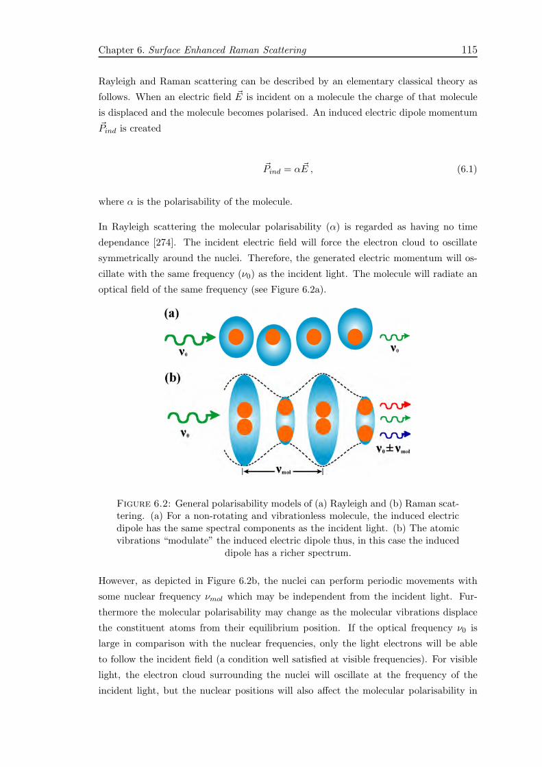
Chapter 6. Surface Enhanced Raman Scattering 115
Rayleigh and Raman scattering can be described by an elementary classical theory as
follows. When an electric field ~E is incident on a molecule the charge of that molecule
is displaced and the molecule becomes polarised. An induced electric dipole momentum
~Pind is created
~Pind = α~E , (6.1)
where α is the polarisability of the molecule.
In Rayleigh scattering the molecular polarisability (α) is regarded as having no time
dependance [274]. The incident electric field will force the electron cloud to oscillate
symmetrically around the nuclei. Therefore, the generated electric momentum will os-
cillate with the same frequency (ν0) as the incident light. The molecule will radiate an
optical field of the same frequency (see Figure 6.2a).
Figure 6.2: General polarisability models of (a) Rayleigh and (b) Raman scat-tering. (a) For a non-rotating and vibrationless molecule, the induced electricdipole has the same spectral components as the incident light. (b) The atomicvibrations “modulate” the induced electric dipole thus, in this case the induced
dipole has a richer spectrum.
However, as depicted in Figure 6.2b, the nuclei can perform periodic movements with
some nuclear frequency νmol which may be independent from the incident light. Fur-
thermore the molecular polarisability may change as the molecular vibrations displace
the constituent atoms from their equilibrium position. If the optical frequency ν0 is
large in comparison with the nuclear frequencies, only the light electrons will be able
to follow the incident field (a condition well satisfied at visible frequencies). For visible
light, the electron cloud surrounding the nuclei will oscillate at the frequency of the
incident light, but the nuclear positions will also affect the molecular polarisability in

Chapter 6. Surface Enhanced Raman Scattering 116
such a way that the amplitude of the electron cloud oscillation will be modulated by
the slow nuclear oscillations. Therefore the polarisability has a time dependence of the
nuclear frequencies. It follows that the scattered light contains frequency components
corresponding to the incident light ν0 as well as the frequencies corresponding to the
nuclear vibrations ν0 ± νmol. These new optical frequencies correspond to the Raman
scattered fields. Moreover, if the molecule is in a stationary state, each atom will feel dif-
ferent forces from the oscillating electrons. This will excite the molecule to a vibrational
state and therefore will also radiate Raman frequencies. It is clear that, if the inten-
sity of the incident light is increased, the molecule will oscillate with higher amplitude,
equation (6.1), and this will increase the probability of molecular transitions. However,
the probability of inducing vibrational transitions is low because the electrons oscillate
much faster than the heavy atoms. Thus, the Raman scattering is weaker than Rayleigh
scattering; the probability of Raleigh scattering is 1 in 105 while the probability of one
photon suffering Raman scattering is 1 in 107.
As described by the Boltzmann, the population in the excited state differs from that
of the ground state by approximately the factor exp(−∆E/kT ). Thus the intensity
of the anti-Stokes and Stokes Raman signals is generally not the same. Since ∆E
is generally large for vibrational transitions (see Figure 6.1) the anti-Stokes vibrational
bands are very weak in comparison to the Stokes bands. On the other hand, for rotational
transitions, ∆E/kT is often small and therefore the Stokes and anti-Stokes rotational
bands are often of comparable intensity. With this simple classical description of the
Raman effect, it is easy to understand that the Raman signal is independent of the
exciting frequency and depends on the normal vibrational frequencies of a molecule
which are determined by the kind of atoms, bonds strength and configuration of the
molecule. Therefore it is commonly said that the Raman spectrum provides a structural
“fingerprint” of the molecule.
6.1.1 Theory of the Raman Effect
Although a classical description of the Raman process gives an important qualitative
explanation of the effect, it does not provide quantitative information. In order to obtain
a quantitative explanation of the Raman effect a quantum mechanical description of the
process is required. Although such an analysis is out of the scope of this thesis, the form
of the final expressions for the intensity of the Raman fields will be briefly discussed.
The quantum mechanical treatment considers the perturbation of the wave-functions of
the molecule by the incident electrical field; it calculates the induced transition moment
associated with a transition between the initial state (n) and the final state (m), which
may be written as follows [275]:
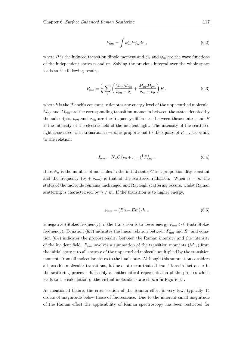
Chapter 6. Surface Enhanced Raman Scattering 117
Pnm =
∫
ψ∗mPψndτ , (6.2)
where P is the induced transition dipole moment and ψn and ψm are the wave functions
of the independent states n and m. Solving the previous integral over the whole space
leads to the following result,
Pnm =1
h
∑
r
(
MnrMrm
νrn − ν0+MnrMrm
νrn + ν0
)
E , (6.3)
where h is the Planck’s constant, r denotes any energy level of the unperturbed molecule.
Mnr and Mrm are the corresponding transition moments between the states denoted by
the subscripts, νrn and νrm are the frequency differences between these states, and E
is the intensity of the electric field of the incident light. The intensity of the scattered
light associated with transition n → m is proportional to the square of Pnm, according
to the relation:
Inm = NnC (ν0 + νnm)4 P 2nm . (6.4)
Here Nn is the number of molecules in the initial state, C is a proportionality constant
and the frequency (ν0 + νnm) is that of the scattered radiation. When n = m the
states of the molecule remains unchanged and Rayleigh scattering occurs, whilst Raman
scattering is characterized by n 6= m. If the transition is to higher energy,
νnm = (En− Em)/h , (6.5)
is negative (Stokes frequency); if the transition is to lower energy νnm > 0 (anti-Stokes
frequency). Equation (6.3) indicates the linear relation between P 2nm and E2 and equa-
tion (6.4) indicates the proportionality between the Raman intensity and the intensity
of the incident field. Pnm involves a summation of the transition moments (Mnr) from
the initial state n to all states r of the unperturbed molecule multiplied by the transition
moments from all molecular states to the final state. Although this summation considers
all possible molecular transitions, it does not mean that all transitions in fact occur in
the scattering process. It is only a mathematical representation of the process which
leads to the calculation of the virtual molecular state shown in Figure 6.1.
As mentioned before, the cross-section of the Raman effect is very low, typically 14
orders of magnitude below those of fluorescence. Due to the inherent small magnitude
of the Raman effect the applicability of Raman spectroscopy has been restricted for
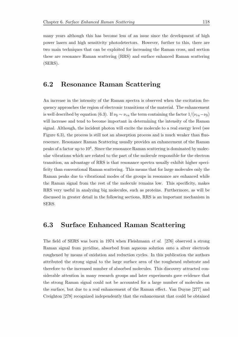
Chapter 6. Surface Enhanced Raman Scattering 118
many years although this has become less of an issue since the development of high
power lasers and high sensitivity photodetectors. However, further to this, there are
two main techniques that can be exploited for increasing the Raman cross, and section
these are resonance Raman scattering (RRS) and surface enhanced Raman scattering
(SERS).
6.2 Resonance Raman Scattering
An increase in the intensity of the Raman spectra is observed when the excitation fre-
quency approaches the region of electronic transitions of the material. The enhancement
is well described by equation (6.3). If ν0 ∼ νrn the term containing the factor 1/(νrn−ν0)
will increase and tend to become important in determining the intensity of the Raman
signal. Although, the incident photon will excite the molecule to a real energy level (see
Figure 6.3), the process is still not an absorption process and is much weaker than fluo-
rescence. Resonance Raman Scattering usually provides an enhancement of the Raman
peaks of a factor up to 104. Since the resonance Raman scattering is dominated by molec-
ular vibrations which are related to the part of the molecule responsible for the electron
transition, an advantage of RRS is that resonance spectra usually exhibit higher speci-
ficity than conventional Raman scattering. This means that for large molecules only the
Raman peaks due to vibrational modes of the groups in resonance are enhanced while
the Raman signal from the rest of the molecule remains low. This specificity, makes
RRS very useful in analyzing big molecules, such as proteins. Furthermore, as will be
discussed in greater detail in the following sections, RRS is an important mechanism in
SERS.
6.3 Surface Enhanced Raman Scattering
The field of SERS was born in 1974 when Fleishmann et al. [276] observed a strong
Raman signal from pyridine, absorbed from aqueous solution onto a silver electrode
roughened by means of oxidation and reduction cycles. In this publication the authors
attributed the strong signal to the large surface area of the roughened substrate and
therefore to the increased number of absorbed molecules. This discovery attracted con-
siderable attention in many research groups and later experiments gave evidence that
the strong Raman signal could not be accounted for a large number of molecules on
the surface, but due to a real enhancement of the Raman effect. Van Duyne [277] and
Creighton [278] recognized independently that the enhancement that could be obtained
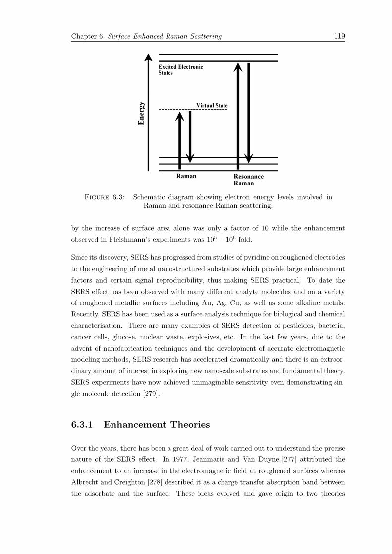
Chapter 6. Surface Enhanced Raman Scattering 119
Figure 6.3: Schematic diagram showing electron energy levels involved inRaman and resonance Raman scattering.
by the increase of surface area alone was only a factor of 10 while the enhancement
observed in Fleishmann’s experiments was 105 − 106 fold.
Since its discovery, SERS has progressed from studies of pyridine on roughened electrodes
to the engineering of metal nanostructured substrates which provide large enhancement
factors and certain signal reproducibility, thus making SERS practical. To date the
SERS effect has been observed with many different analyte molecules and on a variety
of roughened metallic surfaces including Au, Ag, Cu, as well as some alkaline metals.
Recently, SERS has been used as a surface analysis technique for biological and chemical
characterisation. There are many examples of SERS detection of pesticides, bacteria,
cancer cells, glucose, nuclear waste, explosives, etc. In the last few years, due to the
advent of nanofabrication techniques and the development of accurate electromagnetic
modeling methods, SERS research has accelerated dramatically and there is an extraor-
dinary amount of interest in exploring new nanoscale substrates and fundamental theory.
SERS experiments have now achieved unimaginable sensitivity even demonstrating sin-
gle molecule detection [279].
6.3.1 Enhancement Theories
Over the years, there has been a great deal of work carried out to understand the precise
nature of the SERS effect. In 1977, Jeanmarie and Van Duyne [277] attributed the
enhancement to an increase in the electromagnetic field at roughened surfaces whereas
Albrecht and Creighton [278] described it as a charge transfer absorption band between
the adsorbate and the surface. These ideas evolved and gave origin to two theories
Chapter 6. Surface Enhanced Raman Scattering 120
which describe the mechanisms of the enhancement; the electromagnetic theory and the
chemical theory. Although, there has been much discussion on the role and significance of
each contribution, it is generally agreed that the electromagnetic mechanism is the major
contributor to the intensity amplification and that both mechanisms act in parallel, i.e.
multiplicatively. These two theories are discussed in greater detail in the following
sections.
6.3.1.1 Electromagnetic Mechanism
The electromagnetic model is based on the response of nanoscale metallic particles to
light waves. As stated in Chapter 5, the geometrical and material characteristics of
metallic nanoscale particles determine the resonant frequency of the surface plasmons.
Excitation of LSP resonances result in high concentration of the electromagnetic fields at
the surface and selective absorption and scattering of the incident electromagnetic wave.
The electromagnetic enhancement relies on molecules being located within these large
electromagnetic fields. The presence of the nanoparticle electromagnetically modifies
the Raman response of the molecule in such a way that the incident field acting on the
molecules and the emitted Raman light intensities are increased by the polarised surface.
The dipole moment induced in a molecule in close proximity with a metallic feature will
be due to both the incident wave and the Lorentz-Mie elastically scattered field by the
metal particle. In the same way, the Raman radiation at the observer position consists
of the Raman emission of the dipole plus the Raman signal that is re-radiated by the
metal particle causing an enhancement factor of 104 − 106.
In 1980 Kerker et al. [280, 281] proposed a, now-classical, way of investigating the
electromagnetic contribution in SERS. In this model they consider a molecule to behave
as a classical dipole which is located at an arbitrary position (r′) outside a metal sphere of
radius a. When a plane electromagnetic wave of frequency ω0 interacts with the system,
the dipole momentum induced in the molecule will radiate at the Raman frequency ω,
~p = αr~Ep(r
′, ω0) , (6.6)
where αr is the Raman polarisability of the molecule and ~Ep(r′, ω0) is the electric field at
r′ and frequency ω0. Because the metal particle acts as a scatterer of the incident field,
~Ep is composed of the incident field ~Ei(r′, ω0) plus the field scattered by the particle
~ELM (r′, ω0), as calculated by Lorentz-Mie theory
~Ep(r′, ω0) = ~Ei(r
′, ω0) + ~ELM (r′, ω0) . (6.7)
Chapter 6. Surface Enhanced Raman Scattering 121
The Raman radiation at the observation point r is given by
~ER(r, ω0) = ~EDIP (r, ω0) + ~ESC(r, ω0) , (6.8)
where ~EDIP is the field that would be radiated by the oscillating dipole ~p if the sphere
was not present and ~ESC is the secondary scattered field by the sphere. All four fields
must be calculated by solving the appropriate boundary-value problem and they are
given as linear combinations of the Bessel and Hankel functions [280].
The Raman scattering intensity in the radiation zone (r >> r′), is the square of the
far-field amplitude of ER, i.e.,
IR = limkr→∞
∣
∣
∣
∣
ER(r, ω)exp(ikr)
r
∣
∣
∣
∣
2
. (6.9)
The electromagnetic enhancement factor G may now be defined as
G =IRI0R
, (6.10)
where I0R is the Raman intensity in the absence of the metal sphere. In this case the
dipole will only be excited by the incident field Ep = Ei(r′, ω0) and the Raman field is
only due to the oscillating dipole ER = EDIP (r, ω).
This theoretical model can be applied to determining the enhancement of Raman scat-
tering by a molecule on or near the surface of a metal particle of any size. The model
shows high dependence of the enhancement upon the particle size and the excitation
frequency. For small particles, enhancement values of ∼ 106 are predicted and they
show a sharp resonance due almost exclusively to the excitation of the first order dipole-
like plasmon resonance. While, the enhancement factor expected from larger particles
is 102 − 104 and shows broader excitation spectra due to the excitation of high order
multipole plasmon resonances which causes the decrease of both the local field and the
scattered field. The relation between the enhancement to the excitation of surface plas-
mons can be easily appreciated for a molecule near a sphere whose size is optically small
(a << λ0). In this limit, the calculation of the SERS enhancement is rather simple and
is given by
Gem(ω) ≈∣
∣
∣
∣
εm(ω) − εdεm(ω) + 2εd
∣
∣
∣
∣
2 ∣
∣
∣
∣
εm(ω0) − εdεm(ω0) + 2εd
∣
∣
∣
∣
2 (
a
a+ d
)12
, (6.11)
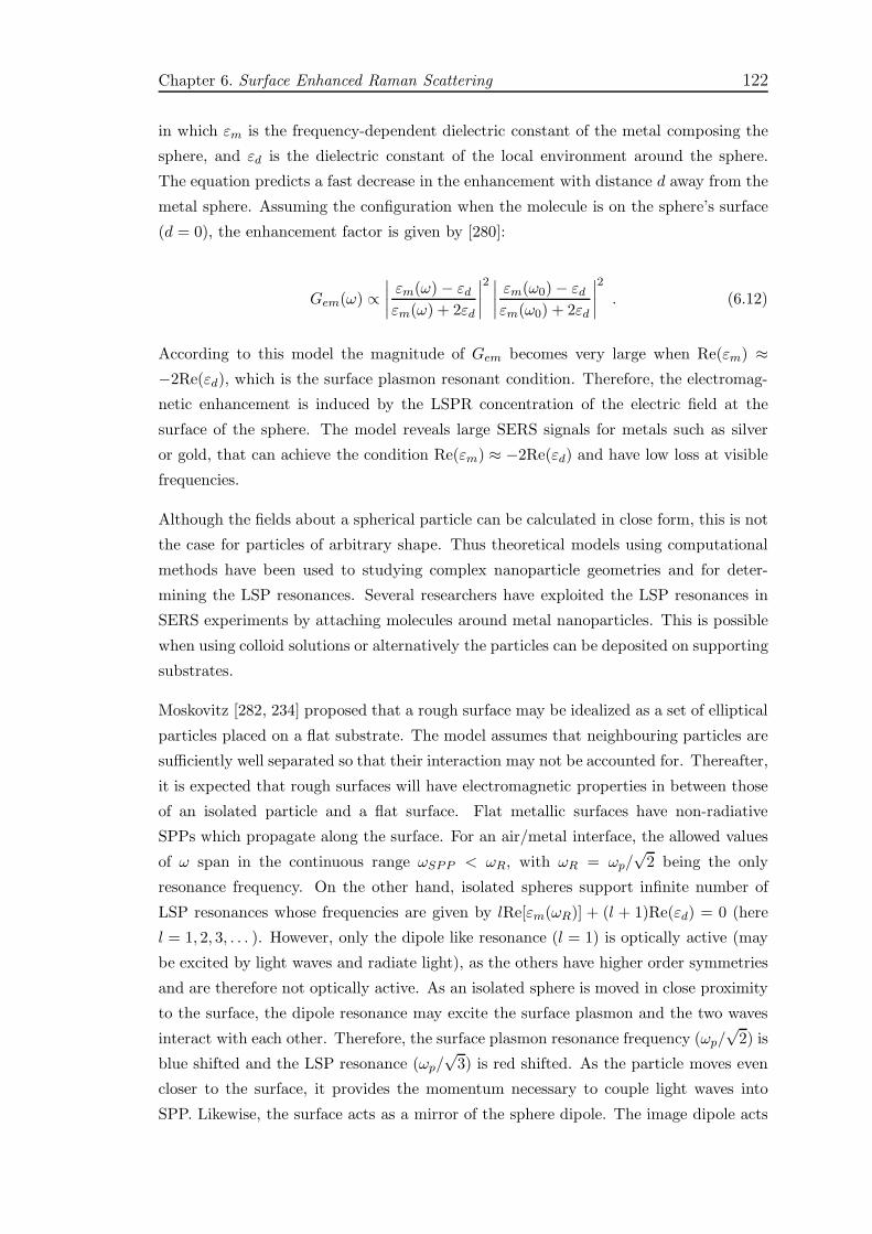
Chapter 6. Surface Enhanced Raman Scattering 122
in which εm is the frequency-dependent dielectric constant of the metal composing the
sphere, and εd is the dielectric constant of the local environment around the sphere.
The equation predicts a fast decrease in the enhancement with distance d away from the
metal sphere. Assuming the configuration when the molecule is on the sphere’s surface
(d = 0), the enhancement factor is given by [280]:
Gem(ω) ∝∣
∣
∣
∣
εm(ω) − εdεm(ω) + 2εd
∣
∣
∣
∣
2 ∣
∣
∣
∣
εm(ω0) − εdεm(ω0) + 2εd
∣
∣
∣
∣
2
. (6.12)
According to this model the magnitude of Gem becomes very large when Re(εm) ≈−2Re(εd), which is the surface plasmon resonant condition. Therefore, the electromag-
netic enhancement is induced by the LSPR concentration of the electric field at the
surface of the sphere. The model reveals large SERS signals for metals such as silver
or gold, that can achieve the condition Re(εm) ≈ −2Re(εd) and have low loss at visible
frequencies.
Although the fields about a spherical particle can be calculated in close form, this is not
the case for particles of arbitrary shape. Thus theoretical models using computational
methods have been used to studying complex nanoparticle geometries and for deter-
mining the LSP resonances. Several researchers have exploited the LSP resonances in
SERS experiments by attaching molecules around metal nanoparticles. This is possible
when using colloid solutions or alternatively the particles can be deposited on supporting
substrates.
Moskovitz [282, 234] proposed that a rough surface may be idealized as a set of elliptical
particles placed on a flat substrate. The model assumes that neighbouring particles are
sufficiently well separated so that their interaction may not be accounted for. Thereafter,
it is expected that rough surfaces will have electromagnetic properties in between those
of an isolated particle and a flat surface. Flat metallic surfaces have non-radiative
SPPs which propagate along the surface. For an air/metal interface, the allowed values
of ω span in the continuous range ωSPP < ωR, with ωR = ωp/√
2 being the only
resonance frequency. On the other hand, isolated spheres support infinite number of
LSP resonances whose frequencies are given by lRe[εm(ωR)] + (l + 1)Re(εd) = 0 (here
l = 1, 2, 3, . . . ). However, only the dipole like resonance (l = 1) is optically active (may
be excited by light waves and radiate light), as the others have higher order symmetries
and are therefore not optically active. As an isolated sphere is moved in close proximity
to the surface, the dipole resonance may excite the surface plasmon and the two waves
interact with each other. Therefore, the surface plasmon resonance frequency (ωp/√
2) is
blue shifted and the LSP resonance (ωp/√
3) is red shifted. As the particle moves even
closer to the surface, it provides the momentum necessary to couple light waves into
SPP. Likewise, the surface acts as a mirror of the sphere dipole. The image dipole acts

Chapter 6. Surface Enhanced Raman Scattering 123
on the sphere exciting multipolar modes which are otherwise not optically accessible.
The resonance spectrum of the system as a whole thus becomes richer than in the case
when the two objects are independent.
In addition, consider the case in which two particles are close to each other, the sys-
tem will present extra plasmon resonances due to electromagnetic coupling between the
particles. Presumably the energy concentrated in the gap between them will be high
and therefore will produce even higher enhancements. By calculating the electromag-
netic fields at various points in a system comprising more than one particle, there have
been some extensions to the theory to treat more realistic SERS substrates. In general,
the fields located between two nanoparticles are even higher than those near isolated
structures, implying further SERS enhancements [283, 284].
The electromagnetic theory has been able to account for a large number of features of
SERS. These include, the observation of an enhancement at some distance of the scatter
molecule from the surface, the high sensitivity of the enhancement to the degree of
surface roughness, the fact that only coinage metals produced large effects, the angular
dependance of the enhancement, and the negligible enhancement at a flat surface, etc.
Many of the surface treatments used to fabricate SERS substrates produce a surface
covered with particles fairly similar to ellipsoids, so that the Mie theory has been able to
qualitatively predict many of their features. However, the particles in general have a wide
distribution of sizes and shapes which makes the exact analysis of the optical properties
of SERS substrates very difficult. Therefore for “complex” SERS substrates, consisting
of many particles (more than 4), it has been more fruitful to turn to experiments to
obtain appropriate descriptions of the electromagnetic properties. Indeed, this is the
case for our fibre SERS substrates (to be described in the Chapter 7), that consist of
many particles of different sizes and distributions so that, combined with the complex
3D fibre geometry, make it very challenging to obtain an appropriate description of their
electromagnetic properties.
6.3.1.2 Chemical Enhancement
It has been proved that the electrodynamic model alone cannot completely describe
all the experimental evidence of SERS. For example, the fact that certain types of
molecules, such as pyridine and piperidine, which contain electrons available for bonding
with the surface, displayed enhancement factors greater than other molecules that are
not adsorbed [285], the observation of voltage-dependent SERS intensity of molecules
adsorbed on electrodes, and many other observations [234, 257], seem to be in conflict
with the electromagnetic theory. However, these effects can be explained in terms of
chemical mechanisms which involve first layer metal-molecule interactions. Although
Chapter 6. Surface Enhanced Raman Scattering 124
many possible chemical enhancement theories have been investigated, most of them have
a common theme; resonance Raman scattering via accessible charge transfer between
intermediate states.
Figure 6.4 illustrates how the initial, intermediate and final state of resonance Raman
scattering are modified for adsorbed molecules. The molecular orbitals of chemisorbed
molecules are broadened by the interaction with the free metal electrons and the contin-
uum of metal states can act as intermediate states for lower energy resonance scattering
processes.
Figure 6.4: Energy levels scheme for molecule-metal complex. The discretemolecular levels of the free molecule are changed due to chemisorption ef-fects. The metal’s Fermi energy lies approximately in the middle between thehigher occupied molecular (HOMO) and the lower unoccupied molecular or-bitals (LUMO) of the molecule. The possible charge transfer paths are shown.
Resonance Raman scattering, attributed to electron transitions in a free molecules (path
(a) in Figure 6.4), can only be excited by ultraviolet photons, however, when consider-
ing the molecule-metal system as a whole, charge transfer transitions may be possible
at lower energies in the visible region of the spectrum. Two new possibilities of charge
transfer could be envisioned in the system. Electrons can be excited from the molecule
HOMO to unfilled metal orbitals above the Fermi energy (molecule-metal charge trans-
fer, path (b)), or transitions in which free electrons are transferred from the metal con-
duction band to the LUMO in the molecule (metal-molecule charge transfer, path (c)).
This chemical theory has been strengthened by the observation of low energy electronic
absorption bands in mono layer metal-molecule systems [286, 287, 288] by means of
electron energy loss spectroscopy. Moreover, spectrochemical experiments have proved
that the metal-molecule charge transfer excitation is red shifted upon making the elec-
tron potential more negative (increasing the Fermi level). Even though the chemical

Chapter 6. Surface Enhanced Raman Scattering 125
enhancement may be observed on atomically smooth metal surfaces, the presence of
nanoscale features on the film provides an easier route for the hot electrons to the ad-
sorbed molecule and facilitates the generation of hot electrons in the metal. Therefore
the chemical model predicts that the enhancement is more effective when the surface is
rough, whereas for electromagnetic enhancement, nanoscale roughness is essential.
In general it is thought that the chemical mechanisms can amplify the Raman scattering
cross section by a factor of 10-100 and although this is small compared to electromagnetic
mechanisms, the effects multiply so that the chemical contribution is of great importance
if high enhancement factors (> 106) are to be obtained.

Chapter 7
Metal Modified Optical Fibres
The previous two chapters have provided an introduction to the field of plasmonics and
one of its most fruitful applications; SERS. This chapter focuses on the optical charac-
terisation of MOFs coated with silver nanoparticles. These fibres allow the excitation of
surface plasmons by optical guided modes. The fibre geometry offers significant benefits
over conventional plasmonic planar structures in that it simplifies the coupling to the
plasmon modes and, due to the waveguiding capabilities of MOFs, the optical guided
modes offer extended electromagnetic interaction lengths to excite multiple plasmon res-
onances along the fibre. Investigations of the SERS capabilities of these structures have
shown large enhancements in the Raman spectra of target molecules absorbed on the
metal surface. The novelty and practicability of the metal-functionalised MOFs sub-
strates opens up new possibilities for the next generation of in-fibre photonic/plasmonic
devices.
7.1 Introduction
The incorporation of metals into a MOF geometry enables the integration of photon
transport with the active plasmonic region to yield completely integrated devices with
unique excitation and detection capabilities. All-fibre devices offer a number of advan-
tages over conventional planar plasmonic structures in that they are cheap, compact,
robust, flexible and are compatible with existing optical fibre systems.
Due to the momentum mismatch between light and plasmons propagating along the
metal/air interface of thin films, plasmonic devices based on a 2D geometry typically
require the use of a prism or coupling elements to phase match the incoming radiation
with surface plasmon waves adding bulk and complexity (see Chapter 5). By exploiting
126
Chapter 7. Metal Modified Optical Fibres 127
the unique guiding geometry of MOFs, the silica core can be thought of as a matching
device, which increases the momentum of a photon and permits the coupling between
guided optical modes and plasmons on the air/metal interface. Based on this approach,
a number of theoretical studies have been conducted to investigate the transmission
properties of metal-dielectric MOF, ranging from fibres with thin-smooth coatings on
the capillary walls to solid nanowire inclusions [289, 290, 291]. The results have shown
that, by carefully choosing the fibre structure and metal coating, it is possible to tune the
wavelength and the number of plasmon resonances, as well as to control the fibre loss.
Because the modal properties of MOFs can be tailored, the problem of phase matching
can be easily circumvented by engineering the fibre geometry. By having a multimode
fibre, which allows the propagation of higher order modes each with a different propa-
gation constant, the coupling to the plasmon modes is even easier. However the fibres
used in the following experiments have been impregnated with granular coatings rather
than smooth-thin coatings. Thus localized surface plasmons resonances rather than sur-
face plasmon waves are expected to exist in these structures, as will be described in
the following section. However, future experiments will be devoted to investigate the
plasmonic properties of MOFs with smooth coatings.
MOFs with metal coatings on the internal capillary walls offer a number of advantages
over earlier investigations of plasmon-photon interaction in optical fibres. In these pre-
vious studies, the interaction between the core guided light and plasmons was achieved
by depositing metal films on the outside of either a tapered fibre or on a window etched
into the cladding [292, 293, 294, 295, 296, 297, 298, 299]. Metal-modified MOFs are not
only more robust and easier to fabricate but also the active region is isolated, via the
silica walls, from the surrounding environment.
The fibres used in this chapter are functionalised using the high pressure chemical depo-
sition technique, described in Section 3.7. During the deposition processes the fibres were
heated to ∼ 200 C, with the organometallic silver precursor dissolved in high-pressure
heptane. A variety of MOFs structures are investigated and control of the deposition
profiles in these fibres is obtained by tuning the experimental parameters such as the
temperature, precursor concentration, flow rate and deposition time to yield a range of
particle sizes, from tens to hundreds of nanometres, and profiles that vary from sparse
nanoparticles to thin granular films [300]. For example, the SEM micrographs shown
in Figure 7.1 reveal that a thin film with silver particles is annularly deposited inside
the fibre capillaries and that, by changing the silver precursor concentration and the
deposition time, silver nanoparticle coating thicknesses of (a) ∼ 200 nm, (b) ∼ 300 nm
and (c) ∼ 500 nm are also formed. SEM micrographs taken at section intervals along
5 cm samples show a similar deposition profile along their length.

Chapter 7. Metal Modified Optical Fibres 128
Figure 7.1: Silver deposition within the holes of a honeycomb fibre with ahexagonal lattice, the hole size is ∼ 7µm in diameter and the pitch is ∼ 12µm.(a) Thin deposition fibre, scale bar 1µm. (b) Medium deposition, scale bar1µm. (c) Thick deposition, scale bar 1µm. (d) Empty fibre template, scale bar
is 40µm
7.2 Transmission Properties of MOFs with Metal
Inclusions
One of the major problems of plasmonic devices incorporating optical waveguides is
how to couple optical energy from guided modes into surface plasmon modes, which
exist on the air/metal interface. If the metal is deposited as a smooth film then this
requires phase matching of the two modes. However, the strict phase matching require-
ments can be relaxed if instead the metal is deposited as nanoparticles, as described in
Chapter 5. Under these conditions the plasmon modes will be localized on the surface
of the particles and can be excited simply by launching light on or near the resonant
wavelength, independent of the wavevector of the guided mode. Significantly, localized
surface plasmon modes can generate even higher electromagnetic enhancements owing
to the strong 3D confinement. The silver profiles achieved in the fibres, shown in Figure
7.1, are granular rather than smooth which suggests that indeed only localized surface
plasmon modes will be excited. Efficient coupling to these modes can be ensured by
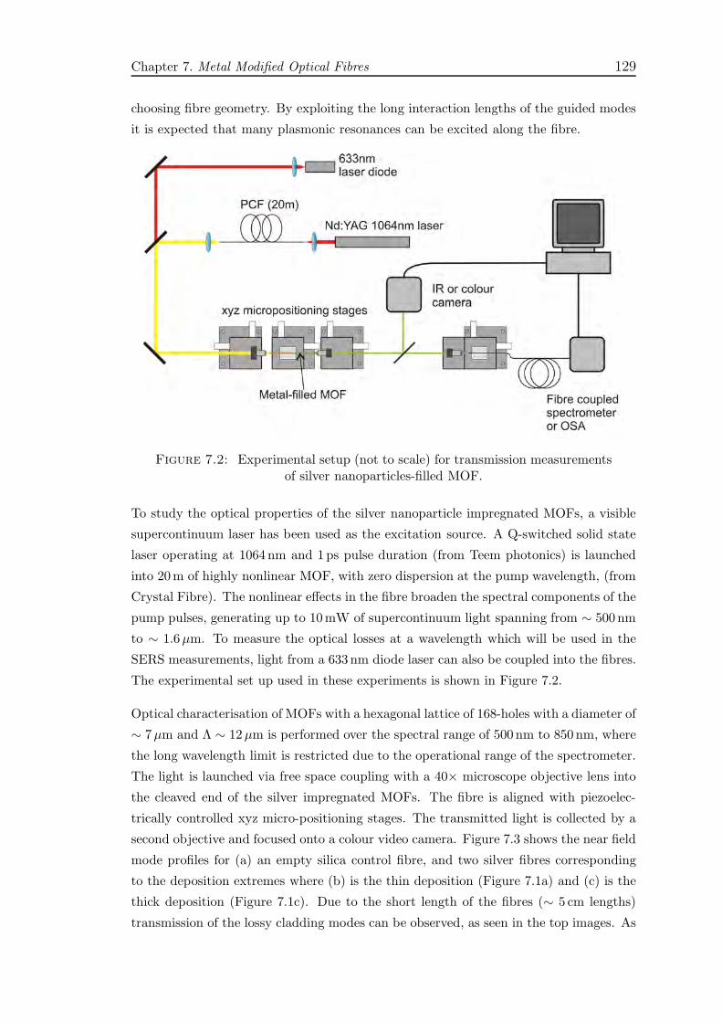
Chapter 7. Metal Modified Optical Fibres 129
choosing fibre geometry. By exploiting the long interaction lengths of the guided modes
it is expected that many plasmonic resonances can be excited along the fibre.
Figure 7.2: Experimental setup (not to scale) for transmission measurementsof silver nanoparticles-filled MOF.
To study the optical properties of the silver nanoparticle impregnated MOFs, a visible
supercontinuum laser has been used as the excitation source. A Q-switched solid state
laser operating at 1064 nm and 1ps pulse duration (from Teem photonics) is launched
into 20m of highly nonlinear MOF, with zero dispersion at the pump wavelength, (from
Crystal Fibre). The nonlinear effects in the fibre broaden the spectral components of the
pump pulses, generating up to 10mW of supercontinuum light spanning from ∼ 500 nm
to ∼ 1.6µm. To measure the optical losses at a wavelength which will be used in the
SERS measurements, light from a 633 nm diode laser can also be coupled into the fibres.
The experimental set up used in these experiments is shown in Figure 7.2.
Optical characterisation of MOFs with a hexagonal lattice of 168-holes with a diameter of
∼ 7µm and Λ ∼ 12µm is performed over the spectral range of 500 nm to 850 nm, where
the long wavelength limit is restricted due to the operational range of the spectrometer.
The light is launched via free space coupling with a 40× microscope objective lens into
the cleaved end of the silver impregnated MOFs. The fibre is aligned with piezoelec-
trically controlled xyz micro-positioning stages. The transmitted light is collected by a
second objective and focused onto a colour video camera. Figure 7.3 shows the near field
mode profiles for (a) an empty silica control fibre, and two silver fibres corresponding
to the deposition extremes where (b) is the thin deposition (Figure 7.1a) and (c) is the
thick deposition (Figure 7.1c). Due to the short length of the fibres (∼ 5 cm lengths)
transmission of the lossy cladding modes can be observed, as seen in the top images. As

Chapter 7. Metal Modified Optical Fibres 130
expected, there is a clear increase in the absorption of the light in the cladding as we
move to thicker silver depositions as well as some wavelength selective absorption.
Figure 7.3: Near field images of the fundamental mode of (a) an empty silicafibre, (b) a thin silver coated fibre and (c) a thick silver coated fibre. Top imagesare without filtering to show the cladding modes, bottom images are taken after
a pinhole to isolate the core guided light.
For the spectral measurements the guided core modes were isolated from those of the
lossy cladding modes using a pinhole and the filtered modes are shown in the bottom
images (Figure 7.3). The yellow colour of the light transmitted through the empty fibre
is simply that of the supercontinuum source, confirming that there is no preferential
absorption of the control MOF at any wavelength. Moving to the fibre with a thin silver
deposition, the mode now has hints of colour around the edges suggesting that the silver
absorption has altered its transmission properties. This is even more evident in the
fibre with a thick deposition where there is clearly a strong absorption at the red end
of the spectrum so that the mode looks bright green. To quantify the observations, the
transmitted light is then focused into a collection fibre attached to an Ocean Optics 2000
spectrometer, with a detection range from 340nm to 1000 nm. The resultant spectra
obtained from the two silver fibres, normalized to the light transmitted through the
control fibre, are plotted in Figure 7.4.
The noticeable lack of any strong resonant absorptions, typically associated with lo-
calized surface plasmon excitations, is attributed to the averaging over many particle
sizes, interparticle separations and film thicknesses which can be excited due to the long
interaction distance. The transmission spectrum for the thin deposition fibre shows an
absorption that increases for longer wavelengths. This is in contrast with that of the
thick deposition fibre where now there is a very strong absorption of the red end of the
wavelength range which accounts for the green colour of the mode. The dramatic shift

Chapter 7. Metal Modified Optical Fibres 131
of the absorption to longer wavelengths is not unexpected as it is well known that when
the silver particle size increases the localized plasmon resonances are shifted from blue
to red. Furthermore, when the particle spacings are of the order of nanometres then
the interparticle interactions can shift the absorptions even further to the near infrared
[301].
500 550 600 650 700 750 800 8500
0.2
0.4
0.6
0.8
1.0
Wavelength (nm)
Tra
nsm
issi
on (
a.u.
)
Figure 7.4: Transmitted spectra corresponding to silver impregnated MOFswith a thin deposition (black line) and a thick deposition (grey line), normalized
to the transmission through an empty MOF.
One of the major obstacles to integrating plasmonic waveguiding devices within existing
photonics infrastructures is the large inherent losses associated with surface plasmon
waves, which typically limits device lengths to order of millimeters [289, 270]. However,
by ensuring that most of the guided light is confined to the low loss silica core of MOFs
it is possible to reduce the optical loss of the structures and thus push device lengths
out to the centimetre lengths used in the above measurements. To quantify the losses
corresponding to the various deposition profiles of the silver MOFs shown in Figure
7.1, cut-back measurements using a 633 nm continuous wave (CW) 2mW laser were
performed. As before, the light is free space coupled into the fibres using a 40× objective,
with a second objective being used to collimate the transmitted light. The output
power is measured with a Newport 2832C power meter with a silicon detector head.
The transmission losses for the three fibres were measured to be: (a) ∼ 0.6 dB/cm, (b)
∼ 2.5 dB/cm and (c) ∼ 5 dB/cm. This increase in loss for increasing silver thickness is
as expected, and we attribute the notable low loss of the thin deposition fibre to the
sparseness of the particle deposition. By assuming a 3 dB device loss tolerance, realistic
length scales for these silver fibres are in the range 0.6−5 cm, which are sufficiently long
to be manageably handled. In general, conventional planar plasmon waveguides exhibit
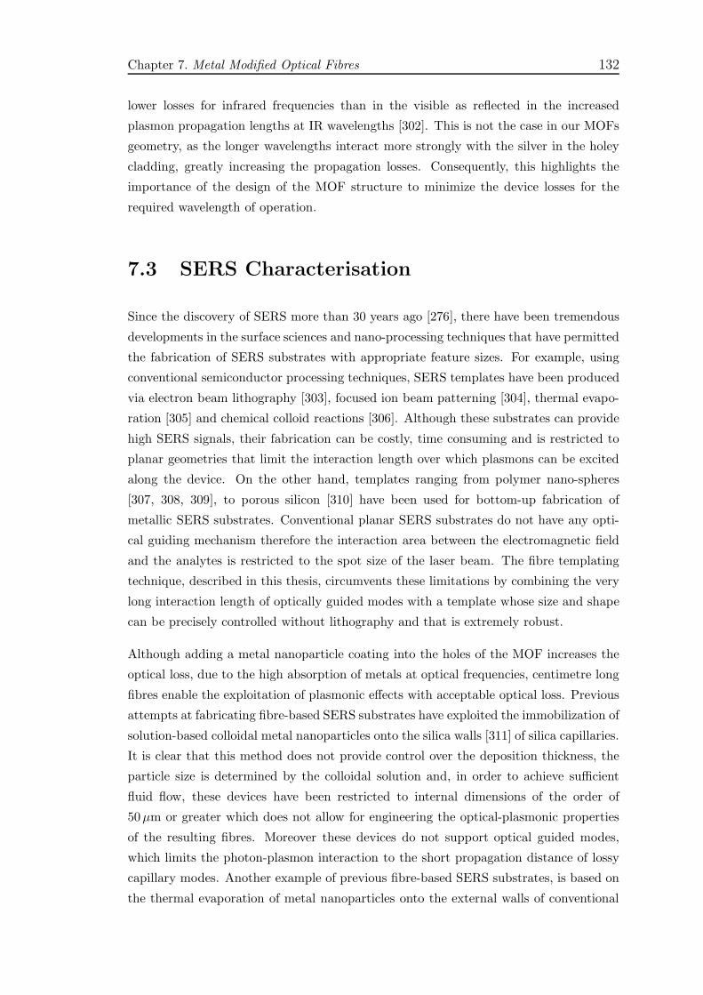
Chapter 7. Metal Modified Optical Fibres 132
lower losses for infrared frequencies than in the visible as reflected in the increased
plasmon propagation lengths at IR wavelengths [302]. This is not the case in our MOFs
geometry, as the longer wavelengths interact more strongly with the silver in the holey
cladding, greatly increasing the propagation losses. Consequently, this highlights the
importance of the design of the MOF structure to minimize the device losses for the
required wavelength of operation.
7.3 SERS Characterisation
Since the discovery of SERS more than 30 years ago [276], there have been tremendous
developments in the surface sciences and nano-processing techniques that have permitted
the fabrication of SERS substrates with appropriate feature sizes. For example, using
conventional semiconductor processing techniques, SERS templates have been produced
via electron beam lithography [303], focused ion beam patterning [304], thermal evapo-
ration [305] and chemical colloid reactions [306]. Although these substrates can provide
high SERS signals, their fabrication can be costly, time consuming and is restricted to
planar geometries that limit the interaction length over which plasmons can be excited
along the device. On the other hand, templates ranging from polymer nano-spheres
[307, 308, 309], to porous silicon [310] have been used for bottom-up fabrication of
metallic SERS substrates. Conventional planar SERS substrates do not have any opti-
cal guiding mechanism therefore the interaction area between the electromagnetic field
and the analytes is restricted to the spot size of the laser beam. The fibre templating
technique, described in this thesis, circumvents these limitations by combining the very
long interaction length of optically guided modes with a template whose size and shape
can be precisely controlled without lithography and that is extremely robust.
Although adding a metal nanoparticle coating into the holes of the MOF increases the
optical loss, due to the high absorption of metals at optical frequencies, centimetre long
fibres enable the exploitation of plasmonic effects with acceptable optical loss. Previous
attempts at fabricating fibre-based SERS substrates have exploited the immobilization of
solution-based colloidal metal nanoparticles onto the silica walls [311] of silica capillaries.
It is clear that this method does not provide control over the deposition thickness, the
particle size is determined by the colloidal solution and, in order to achieve sufficient
fluid flow, these devices have been restricted to internal dimensions of the order of
50µm or greater which does not allow for engineering the optical-plasmonic properties
of the resulting fibres. Moreover these devices do not support optical guided modes,
which limits the photon-plasmon interaction to the short propagation distance of lossy
capillary modes. Another example of previous fibre-based SERS substrates, is based on
the thermal evaporation of metal nanoparticles onto the external walls of conventional

Chapter 7. Metal Modified Optical Fibres 133
step-index fibres [295, 297]. Although, these fibres provide long interaction distances of
the guided modes with the deposited particles, it has the disadvantage that the metal
surface is exposed to the external environment which makes the system unstable and it
must be handled with care. Whereas, MOFs with metal-nanoparticle inclusions, can be
engineering to obtain the desirable optical-plasmonic properties, the silver coatings can
be precisely controlled and are robust. Therefore they represent a promising platform
technology for fully integrated surface enhanced Raman scattering (SERS) sensors.
The metal-nanoparticle fibre substrates were tested for SERS activity using benzenethiol
as the target molecule. Benzenethiol is a suitable molecule for investigating SERS due
to its distinct Raman features, strong affinity for coinage-metal surfaces, and formation
of self-assembled monolayers. The measurements were conducted using a conventional
Renishaw 2000 Raman spectrometer with a 785 nm Ti:sapphire laser excitation source,
operating at an average power of 20mW, and using a 20× microscope objective which
produces a spot size of approximately 5µm in diameter. In all the experiments only the
Stokes signal was measured, as the anti-Stokes process is hundreds of time weaker.
Figure 7.5: Schematic diagram and photograph of the Renishaw 2000 Ramanspectrometer. A 633 nm HeNe laser was also used in SERS experiments.
Figure 7.5 shows a schematic diagram of the Raman spectrometer. As indicated by
the red arrow the excitation laser light is directed into the spectrometer. The light is
then directed through the spatial beam filter. The collimated beam is then reflected
onto the notch filter, where it is directed into the microscope and it is focused onto the
fibre’s cleaved end. The Raman and Rayleigh scattered light and, reflected laser light
are collected by the microscope and directed to the notch filter and through to the laser

Chapter 7. Metal Modified Optical Fibres 134
filter where the remaining laser light and Rayleigh scattering are eliminated. The Raman
scattering then goes through to the monochromator whose entrance slit is set to 50µm
for all the measurements reported in this thesis. The diffracted beam is collected by the
CCD detector. The Renishaw 2000 system can perform static or extended scans. A static
scan records a spectrum from a narrow range of wavenumbers and the monochromator
grating assembly remains still. Extended scans require movement of the grating and
a spectrum can be recorded over a much broader range of wavenumbers, however the
minimum integration time is 10 s for one scan. In order to normalize the intensity of
the SERS signal obtained in different experiments, the intensity of the SERS spectra
presented in this chapter is measured in counts/power/second where the photon counts
detected by the CCD detector are divided by the power of the excitation laser and the
integration time used in the experiment.
The SERS responde of two fibre template designs was investigated, an hexagonal array
containing 18 × 5µm diameter air holes with a 20µm silica core and a hexagonal array
with 168× 12µm holes and a 15µm core. Samples from the resulting metal-filled fibres
were prepared in ∼ 15mm lengths. Thus, for a 15 cm long silver coated fibre ∼ 10 SERS
substrates were obtained so that the individual fabrication cost of the substrates is low
whilst the production rate is high. The sectioned samples were then treated with a
drop of 1mM benzenethiol solution in ethanol (purity > 98% Aldrich and HPLC-grade
Aldrich, respectively). After the solvent had evaporated, the fibres were rinsed and then
soaked in ethanol for 30 minutes. This procedure ensures that, at most, a monolayer
of benzenethiol was present on the silver coating inside the fibres during the Raman
measurements. In this process the sulphur atom chemisorbs onto the metal surface and
the hydrogen atom is released thus changing the vibrational modes of the molecule.
Figure 7.6 compares a typical SERS spectrum from (a) a metal functionalised MOF with
that of (b) a bulk Raman spectrum of neat benzenethiol. The distinctive characteristics
of both spectra can be assigned to the aromatic ring vibrations. The bands at 1586 cm−1
and 1000 cm−1, in the Raman spectra of neat benzenethiol are redshifted to 1574 cm−1
and 997 cm−1 for the SERS spectra of a monolayer of benzenethiol, due to the adsorption
of the target molecule to the metal surface as shown in the inset of Figure 7.6(a). The
SERS detection of a monolayer of benzenethiol in the silver-nanoparticle coated fibres is
verified from the absence of the bands at 2567 cm−1 and 918 cm−1 in the SERS spectra,
which are attributed to the stretching and bending vibrations of S-H molecular bond,
as expected if all the molecules are attached directly to the silver surface [312].
To illustrate the uniformity of the deposition over the cross-section of the 168-holes
MOFs, the SERS spectra was measured at different positions across the structured
cladding. Under these launch conditions, the fibre modes that are excited are the lossy
cladding modes that exist in the MOF templates because of the large silica fraction of

Chapter 7. Metal Modified Optical Fibres 135
Figure 7.6: (a) SERS signal of benzenethiol on a silver impregnated fibresubstrate, the absence of the S-H bond in the spectrum verifies that all themolecules are attached to the surface, areas enclosed by the red circles. (b)Typical Raman spectra of neat benzenethiol with a schematic of the molecule
shown in the inset.
the cladding (see Figure 7.7a and Figure 7.8c). The benzenethiol molecules that are
absorbed onto the silver nanoparticles within the fibre couple to the LSP modes, thus
releasing Raman scattered photons. The generated Raman photons are collected with
the same objective lens used to focus the incident pump beam. Figure 7.7c shows the
collected spectra corresponding to the coloured positions marked on the SEM micrograph
of Figure 7.7a. A strong signal is observed in all cases and the main vibrational modes
of the target molecule can be assigned as reported in the literature [313] and again,
detection of a monolayer is verified. Additionally, no Raman peaks were observed in
a control fibre where 1mM benzenethiol was impregnated into an empty (silica only)
MOF. For the control fibre, the typical Raman spectra of silica, consisting of a series of
broad peaks separated by 440 cm−1, was observed [314].
A significant feature of the spectra, presented in Figure 7.7c, is that the relative intensity
is higher for the positions which are closer to the core of the fibre. To investigate this, the
incident beam was focused onto the silica cores of the two different fibre templates (168-
holes and 18-holes) to excite low loss guided modes. Figure 7.7b is a SEM micrograph of
the 18-holes fibre. Figure 7.7d shows the measured SERS spectra for the two samples,
together with a control spectrum obtained from a fibre that has no silver impregnation,
clearly illustrating the intense signal detectable in this configuration. Although the
optical guided modes concentrate most of their energy in the core of the fibre, a small part
of the energy is located in the air regions surrounding the core as evanescent fields which
interact with the silver coating and excite surface plasmon along the fibre length [311].
For the choice of pump wavelength, the fibres used in the experiments are multimode so
that various LSP modes may be excited on a range of silver particles sizes.
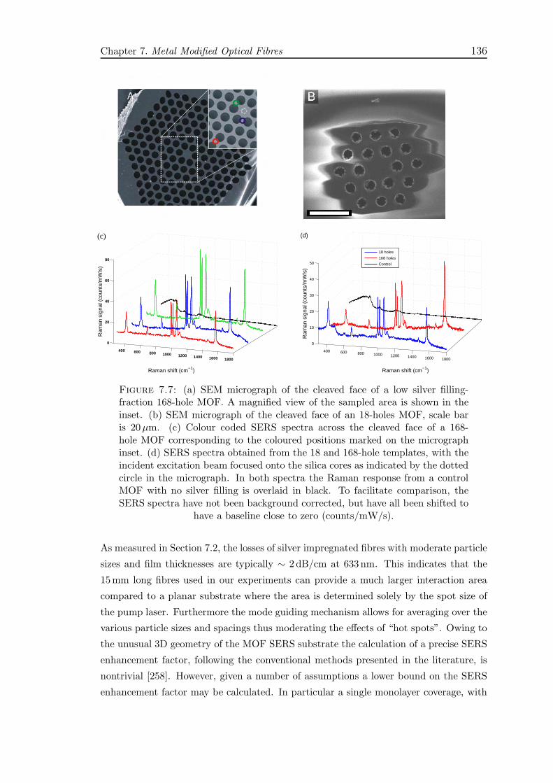
Chapter 7. Metal Modified Optical Fibres 136
400 600 800 1000 1200 1400 1600 1800
0
20
40
60
80
Raman shift (cm−1)
Ram
an s
igna
l (co
unts
/mW
/s)
(c)
400 600 800 1000 1200 1400 1600 1800
0
10
20
30
40
50
Raman shift (cm−1)
Ram
an s
igna
l (co
unts
/mW
/s)
18 holes
168 holes
Control
(d)
Figure 7.7: (a) SEM micrograph of the cleaved face of a low silver filling-fraction 168-hole MOF. A magnified view of the sampled area is shown in theinset. (b) SEM micrograph of the cleaved face of an 18-holes MOF, scale baris 20µm. (c) Colour coded SERS spectra across the cleaved face of a 168-hole MOF corresponding to the coloured positions marked on the micrographinset. (d) SERS spectra obtained from the 18 and 168-hole templates, with theincident excitation beam focused onto the silica cores as indicated by the dottedcircle in the micrograph. In both spectra the Raman response from a controlMOF with no silver filling is overlaid in black. To facilitate comparison, theSERS spectra have not been background corrected, but have all been shifted to
have a baseline close to zero (counts/mW/s).
As measured in Section 7.2, the losses of silver impregnated fibres with moderate particle
sizes and film thicknesses are typically ∼ 2 dB/cm at 633 nm. This indicates that the
15mm long fibres used in our experiments can provide a much larger interaction area
compared to a planar substrate where the area is determined solely by the spot size of
the pump laser. Furthermore the mode guiding mechanism allows for averaging over the
various particle sizes and spacings thus moderating the effects of “hot spots”. Owing to
the unusual 3D geometry of the MOF SERS substrate the calculation of a precise SERS
enhancement factor, following the conventional methods presented in the literature, is
nontrivial [258]. However, given a number of assumptions a lower bound on the SERS
enhancement factor may be calculated. In particular a single monolayer coverage, with

Chapter 7. Metal Modified Optical Fibres 137
a packing density of 6.8 × 10¹⁴ molecules/cm2 [315], over the entire 15mm length was
assumed and the percentage of the fundamental guided mode in the air to was used
to estimate the power in the excitation field. Comparing the SERS measurements to a
standard Raman measurement on neat benzenethiol, the resulting enhancement factor is
estimated to be greater than 104, which compares favourably to enhancements reported
elsewhere in the literature.
Figure 7.8: Calculated mode profile of the 168-hole MOF showing (a) thefundamental guided mode and (b) the cladding filling mode at an excitationwavelength of 785 nm. The figures show the normalized power distributionacross the silica MOF as a function of radial position, as indicated by the dottedlines across the 2D intensity plots shown in the top left insets. The top rightinsets show the distributed modes generated by launching a 633 nm laser intothe control silica (i.e. no silver) fibre as imaged by an Electrophysics 7290A
Vidicon IR camera.
Using the FEM software, the propagation constant and field distribution of the funda-
mental and higher order modes of an empty MOF were calculated. As shown in Figure
7.8a, the low loss fundamental guided mode in the core has only a small fraction of the
overall power propagating in the air, resulting in relatively low excitation of nanoparticle
plasmon resonances per unit (cross-sectional) area when silver is deposited inside the
MOF. However, this is compensated by the long propagation length of the fundamental
mode so that a large number of nanoparticle resonances can be excited adjacent to the
core. Raman photons generated along the fibre are thus efficiently collected and guided
by the high numerical aperture silica core and detected by the spectrometer. Conversely,
in Figure 7.8b an example of a lossy cladding mode is shown which is far more delocal-
ized across the periodic hole array and has a larger component propagating in the air
with little or no power in the core. This results in substantially different behavior as
the area of plasmonic interaction is larger, and many more silver nanoparticles will be
excited per unit area; however, this increased excitation efficiency is offset by the lossy
mode’s shorter propagation distance, resulting in fewer plasmon resonances throughout
the length of the fibre. In addition, the generated Raman photons are not well coupled

Chapter 7. Metal Modified Optical Fibres 138
and localized by the high NA core, resulting in low detection efficiency for this partic-
ular setup. In either scenario, the detected SERS signals obtained with the 168-fibre
are approximately equivalent in magnitude as can be seen by comparing the graphs of
Figure 7.7c and Figure 7.7d (showing the SERS response from various positions on the
cladding and core respectively), suggesting that the relative trade-offs of both modal
excitation conditions roughly balance each other out, for this particular fibre template.
Given the conflicting criteria of many nanoparticle plasmon excitations per unit area,
versus long optical propagation distances and efficient Raman photon collection and
detection, it would at first appear that further improvements to the optical fibre based
substrates will have to operate within these opposing constraints. However, the 168 and
18−hole MOFs used in these experiments are early stage designs and are thus relatively
simple proof-of-principle structures with large, non-optimized feature sizes. Indeed, for
the laser wavelength used in these experiments (785 nm), the large 20µm diameter core
results in very few guided modes with any significant penetration of the optical power
into the air holes. This suggests that in order to combine the desirable properties of
large excitation areas with long propagation distances and efficient collection/detection,
the ideal optical fiber characteristics would exhibit a large NA together with low loss
guided modes that have a large optical component propagating in the voids. These
criteria can be satisfied by a MOF design that has a small core diameter and a large
air fraction honeycomb cladding [316] as this retains the high core-cladding refractive
index contrast required for large NA, but at the same time requires the guided modes
to propagate with a large amount of power in the air due to the small core size.
An important consideration into the practicality of a SERS substrate is its temporal
stability. Silver is regarded as having superior plasmonic properties to gold at visible
wavelengths [216] due to the larger real (negative) part of its dielectric constant and its
smaller imaginary (loss) component. However, as silver is prone to oxidation resulting
in the strong suppression of surface plasmons, it has been largely neglected as a ma-
terial for fabricating SERS substrates with high reproducibility. Despite this potential
problem, the fibre structures demonstrated here have been shown to generate efficient
SERS signals months after they were fabricated, without special storage considerations,
highlighting the temporal stability and mechanical robustness of the substrates.
7.3.1 Fibres with Different Geometries
In order to investigate the above claim of optimised excitation with a small core geom-
etry, a new fibre template was impregnated with silver nanoparticles. A MOF template
based on a 126×1µm hole structure with a small ∼ 1µm diameter silica core (see Figure
7.9) was chosen due to its small dimensions. This fibre structure has a larger overlap
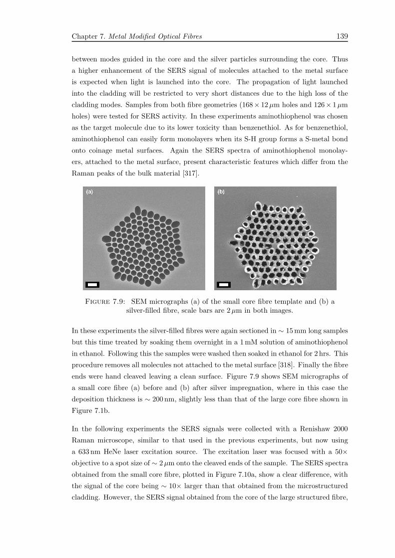
Chapter 7. Metal Modified Optical Fibres 139
between modes guided in the core and the silver particles surrounding the core. Thus
a higher enhancement of the SERS signal of molecules attached to the metal surface
is expected when light is launched into the core. The propagation of light launched
into the cladding will be restricted to very short distances due to the high loss of the
cladding modes. Samples from both fibre geometries (168× 12µm holes and 126× 1µm
holes) were tested for SERS activity. In these experiments aminothiophenol was chosen
as the target molecule due to its lower toxicity than benzenethiol. As for benzenethiol,
aminothiophenol can easily form monolayers when its S-H group forms a S-metal bond
onto coinage metal surfaces. Again the SERS spectra of aminothiophenol monolay-
ers, attached to the metal surface, present characteristic features which differ from the
Raman peaks of the bulk material [317].
Figure 7.9: SEM micrographs (a) of the small core fibre template and (b) asilver-filled fibre, scale bars are 2µm in both images.
In these experiments the silver-filled fibres were again sectioned in ∼ 15mm long samples
but this time treated by soaking them overnight in a 1mM solution of aminothiophenol
in ethanol. Following this the samples were washed then soaked in ethanol for 2 hrs. This
procedure removes all molecules not attached to the metal surface [318]. Finally the fibre
ends were hand cleaved leaving a clean surface. Figure 7.9 shows SEM micrographs of
a small core fibre (a) before and (b) after silver impregnation, where in this case the
deposition thickness is ∼ 200 nm, slightly less than that of the large core fibre shown in
Figure 7.1b.
In the following experiments the SERS signals were collected with a Renishaw 2000
Raman microscope, similar to that used in the previous experiments, but now using
a 633 nm HeNe laser excitation source. The excitation laser was focused with a 50×objective to a spot size of ∼ 2µm onto the cleaved ends of the sample. The SERS spectra
obtained from the small core fibre, plotted in Figure 7.10a, show a clear difference, with
the signal of the core being ∼ 10× larger than that obtained from the microstructured
cladding. However, the SERS signal obtained from the core of the large structured fibre,

Chapter 7. Metal Modified Optical Fibres 140
shown in Figure 7.10a, is similar to that from the holey cladding, as expected from Figure
7.7. Furthermore, owing to the greatly improved interaction between the light and the
silver nanoparticles, the small core fibre exhibits SERS signals more than an order of
magnitude stronger than the large structure when focused in the core. This finding
highlights the possibility of tailoring the plasmon-photon interaction within metal-filled
MOFs via modal overlap engineering.
Figure 7.10: SERS spectra of aminothiophenol obtained from silver impreg-nated MOFs. (a) Spectra from small core MOF template and (b) from largeMOF template. The blue spectra are obtained with the excitation laser focusedonto the silica cores. The spectra plotted in red are the signals obtained with
the incident light focused onto the structured claddings.
7.3.2 Remote SERS Sensing
Following the successful optimisation of the core guided excitation mechanism, the small
core fibre was tested for potential use in remote sensing applications. For this experiment
silver was deposited in the last three centimetres of a 15 cm long fibre. Thus the SERS
active region was confined to the tip of the MOF. The silver end of the fibre was treated
with aminothiophenol using the procedure described previously. The pump laser was
then launched into the fibre core at the empty end, using a 50× objective. The light
propagating down the fibre interacts with the metal modified end, where the SERS signal
of aminothiophenol is excited, and some of the scattered light is guided back to the input
end where it is collected by the same lens. The collected SERS signal is displayed in
Figure 7.11.
Although the SERS signal obtained from the remote sensing experiments presents a high
background such that its intensity is larger than the intensity of the measured vibrational
peaks, definite features of the SERS spectra of aminothiophenol can be recognized as
indicated in Figure 7.11. It is expected that improvements on the deposition profile and
fibre geometry will result in more efficient and sensitive remote SERS sensing devices.
Chapter 7. Metal Modified Optical Fibres 141
SilicaPeak
ATP
Figure 7.11: SERS signal of aminothiophenol obtained in a remote sensingconfiguration.
7.4 Efficient Electrical Characterisation of the
SERS Substrates
In addition to examining their optical properties, silver impregnated MOFs can also be
electrically characterised to establish both the homogeneity and quantity of deposition.
Similarly the SERS signal, detected when analyte molecules are infiltrated within the
structures, can be directly correlated to the deposition profile of the nanoparticles within
the MOFs. Therefore, by assuming a direct correlation between electrical measurements
and SERS response it is possible to use this method as a fast and non-destructive method
of scanning quickly through a number of SERS fibres to find those with optimized
deposition profiles.
Electrical resistivity measurements on two 18-hole fibres with different silver filling frac-
tions were performed. The fibres were prepared by placing indium-gallium eutectic onto
cleaved ends, with the polymer coating removed. This provided a low resistance con-
tact between the fibre and the probe station, as illustrated in the inset of Figure 7.12a.
Figure 7.12 shows the current vs. voltage curves with silver filling fractions (defined
as filled cross-sectional area of each pore) of approximately (a) 40% and (c) 10%, for
different sample lengths. For the fibre with a higher silver filling fraction, the resistance
per millimeter of a 23mm long sample increased slightly from 33.4Ωmm to 36.2Ω/mm
after recleaving to 6mm (Figure 7.12a), whereas for the lower silver filling fraction fibre
the resistance per millimeter decreased from 46.30MΩ/mm at 27mm, to 17.61MΩ/mm
at 18mm and 19.11MΩ/mm at 9mm lengths (Figure 7.12b). This variation of the I-V

Chapter 7. Metal Modified Optical Fibres 142
behavior along the fibre length suggests that the deposition profile is not homogeneous
for the low filling fraction sample.
These electrical measurements can then be related to the SERS response of the fibre
where an inverse correlation between the electrical resistance properties of optical fibres
and the signal strength was observed. This is illustrated in Figures 7.12b and 7.12d
where the signal from the low filling fraction (high resistance) fibre is 3× higher than
the (low resistance) sample with a high filling fraction, which can be attributed in
part to the higher loss in the high filling fraction fibre. This very convenient electrical
characterisation method thus allows us to quickly scan through a number of samples to
establish which deposition profiles are likely to provide a strong Raman response, and
to obtain samples with reproducible SERS response.
Figure 7.12: Current/voltage measurements on various lengths of two 18-holesilver filled MOFs with filling fractions of (a) ∼ 40% and (c) ∼ 10%. Thesamples had been cleaved at the ends and electrical contacts made with InGaeutectic (circuit diagram in top inset of (a)). The lengths corresponding to eachspectrum are given in the insets, together with the calculated sample resistancesbased on an Ohmic model together with control measurements on an unfilledsilica MOF (dashed lines). (b) and (d) display the corresponding SERS response
of the different filling fractions shown in the micrograph insets.
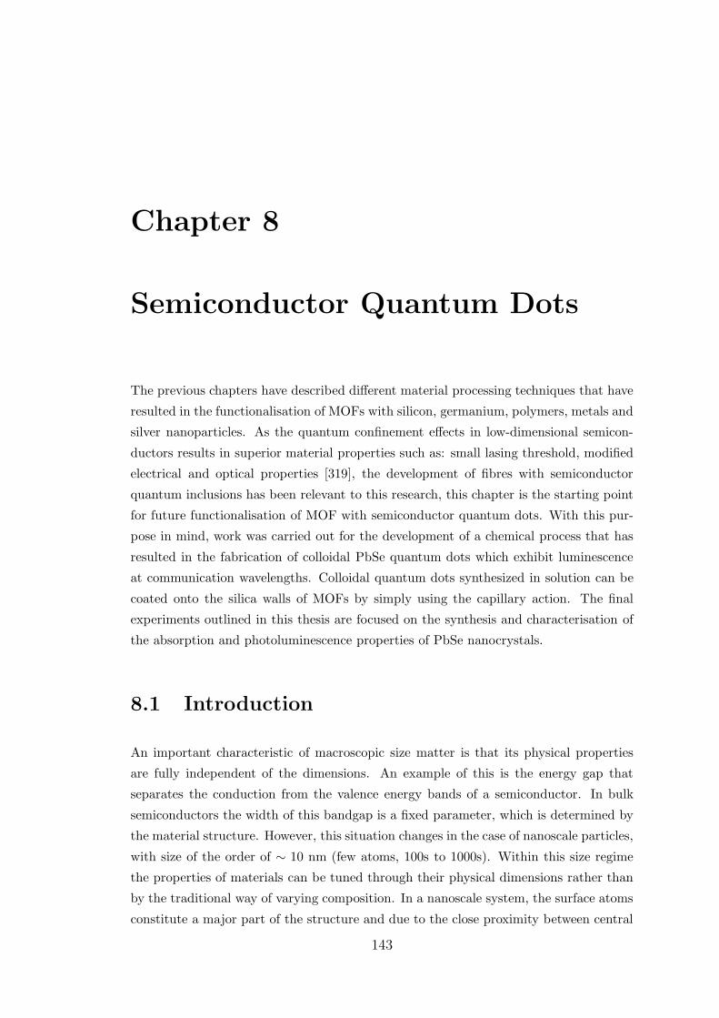
Chapter 8
Semiconductor Quantum Dots
The previous chapters have described different material processing techniques that have
resulted in the functionalisation of MOFs with silicon, germanium, polymers, metals and
silver nanoparticles. As the quantum confinement effects in low-dimensional semicon-
ductors results in superior material properties such as: small lasing threshold, modified
electrical and optical properties [319], the development of fibres with semiconductor
quantum inclusions has been relevant to this research, this chapter is the starting point
for future functionalisation of MOF with semiconductor quantum dots. With this pur-
pose in mind, work was carried out for the development of a chemical process that has
resulted in the fabrication of colloidal PbSe quantum dots which exhibit luminescence
at communication wavelengths. Colloidal quantum dots synthesized in solution can be
coated onto the silica walls of MOFs by simply using the capillary action. The final
experiments outlined in this thesis are focused on the synthesis and characterisation of
the absorption and photoluminescence properties of PbSe nanocrystals.
8.1 Introduction
An important characteristic of macroscopic size matter is that its physical properties
are fully independent of the dimensions. An example of this is the energy gap that
separates the conduction from the valence energy bands of a semiconductor. In bulk
semiconductors the width of this bandgap is a fixed parameter, which is determined by
the material structure. However, this situation changes in the case of nanoscale particles,
with size of the order of ∼ 10 nm (few atoms, 100s to 1000s). Within this size regime
the properties of materials can be tuned through their physical dimensions rather than
by the traditional way of varying composition. In a nanoscale system, the surface atoms
constitute a major part of the structure and due to the close proximity between central
143
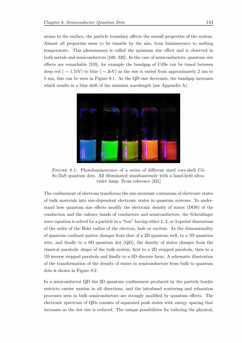
Chapter 8. Semiconductor Quantum Dots 144
atoms to the surface, the particle boundary affects the overall properties of the system.
Almost all properties seem to be tunable by the size, from luminescence to melting
temperature. This phenomenon is called the quantum size effect and is observed in
both metals and semiconductors [100, 320]. In the case of semiconductors, quantum size
effects are remarkable [319], for example the bandgap of CdSe can be tuned between
deep red ( ∼ 1.7eV) to blue ( ∼ 3eV) as the size is varied from approximately 2 nm to
5 nm, this can be seen in Figure 8.1. As the QD size decreases, the bandgap increases
which results in a blue shift of the emission wavelength (see Appendix A).
Figure 8.1: Photoluminescence of a series of different sized core-shell Cd-Se/ZnS quantum dots. All illuminated simultaneously with a hand-held ultra-
violet lamp. From reference [321]
The confinement of electrons transforms the size-invariant continuum of electronic states
of bulk materials into size-dependent electronic states in quantum systems. To under-
stand how quantum size effects modify the electronic density of states (DOS) of the
conduction and the valence bands of conductors and semiconductors, the Schrodinger
wave equation is solved for a particle in a “box” having either 1, 2, or 3 spatial dimensions
of the order of the Bohr radius of the electron, hole or exciton. As the dimensionality
of quantum confined matter changes from that of a 2D quantum well, to a 1D quantum
wire, and finally to a 0D quantum dot (QD), the density of states changes from the
classical parabolic shape of the bulk system, first to a 2D stepped parabola, then to a
1D inverse stepped parabola and finally to a 0D discrete form. A schematic illustration
of the transformation of the density of states in semiconductors from bulk to quantum
dots is shown in Figure 8.2.
In a semiconductor QD the 3D quantum confinement produced by the particle border
restricts carrier motion in all directions, and the intraband scattering and relaxation
processes seen in bulk semiconductors are strongly modified by quantum effects. The
electronic spectrum of QDs consists of separated peak states with energy spacing that
increases as the dot size is reduced. The unique possibilities for tailoring the physical,
Chapter 8. Semiconductor Quantum Dots 145
electronic and optical properties of zero dimensional systems have attracted a diverse
range of potential applications for semiconductor QDs, most notably in precise wave-
length light-emitting diodes [322], optical gain media [323], biological fluorescence la-
beling [324], full color displays, electronic switches and recording media [325]. CdSe
and CdS quantum dots systems have been successful characterised for photonic appli-
cations at visible wavelengths. Klimov and co-workers have demonstrated optical gain
phenomena, such as amplified spontaneous emission in thin films of infrared-emitting
PbSe nanocrystals [326]. PbSe quantum dots are among the few materials that can pro-
vide size-quantized exciton transitions at telecommunications wavelengths. In addition,
they have relatively large Bohr radii that can readily provide access to the quantum
confinement regime at room temperature [327]. Research into applications of colloidal
quantum dots has largely focussed on optoelectronic planar devices. However, due to
the interesting optical properties of PbSe quantum dots in the telecommunications win-
dows, it is motivating to introduce these nanostructures into MOFs for the development
of QDs based optoelectronic fibre devices.
Figure 8.2: Density of states as a function of energy of quantum-confinedsemiconductor structures. As the degree of confinement increases the carriersoccupy increasingly fewer energy levels. QDs have a peak-like density of statesenabling a higher concentration of carriers to contribute to the band-edge opticalmaterial emission. This provides important applications for quantum systems,in principle, ultralow threshold laser diodes [328]. σ(E) and δ(E) denotes the
step and Dirac-delta functions respectively.
8.2 Synthesis of PbSe Quantum Dots
Although the size dependence of the optical properties of metals has been studied since
the 19th century (see Chapter 5), this is not the case for semiconductor nanocrystals. It
Chapter 8. Semiconductor Quantum Dots 146
was not until the last two decades that intense research aimed at making monodisperse
semiconductor quantum dots, in order to study the size evolution of their chemical
and physical properties, has been carried out. The fabrication of these QDs has been
approached by two different techniques. The first and most common and conventional,
is a physical top-down approach in which the dimension of bulk material is physically
reduced. Some examples include lithography and molecular beam epitaxy. The second,
is the wet-chemical technique in which a quantum dot is formed by self-assembly of the
constituent atoms [319]. The most widely used wet-chemistry method is often referred
to as arrested nucleation and growth. This process is based on chemical replacement
reactions between chemical compounds providing metal ions (Cd2+, Zn2+, Pb2+, etc.)
and those containing chalcogenide ions (S2−, Se2−, Te2−, etc.). The general reaction
scheme, for the example of PbSe, reads as [329]
N(Pb2++Se2−) → (PbSe)N (8.1)
The chemical synthesis of semiconductor QDs usually results in small nanoclusters
capped by an organic monolayer which are rapidly nucleated and then slowly grown
in solution. It allows for the fabrication of dots down to the truly atomic regime of 1 nm
to about 20 nm, thus providing easy access to quantum size effects. Due to the organic
capping layer, these QDs have numerous superior attributes compares to lithography
synthesised QDs. For instance, the organic capping layer provides the nanocluster with
solubility properties in a wide range of nonpolar and polar solvents, control over sur-
face functionality and chemical passivation of the surface. In addition, the dots can be
processed much faster and cheaper than with MBE, or any other top-down lithographic
method and for the purposes of this thesis QDs in solution can be deposited inside
MOFs.
Following on from a series of experiments concerning the organometallic synthesis of
capped semiconductor nanocrystals by wet-chemistry [330, 331, 332], several different
synthesis strategies have been reported for narrow band-gap II-VI infrared emitters.
The most notable of these being the work of Wehrenberg et al. [333] and Du et al.
[327]. The basic idea behind the synthesis is to rapidly create a large number of viable
PbSe seeds, from suitable precursors at saturation, and then allow these seeds to grow
at the same rate and end up with TOP capped PbSe nanoclusters (TOP, trioctylphos-
phine, is a surfactant-ligand-solvent). The most commonly used process, as described by
Wehrenberg, requires the synthesis of stable precursors of lead and selenium, which are
then combined at room temperature under an inert atmosphere. This stock solution is
then rapidly injected into a comparable volume of a coordinating solvent, or surfactant,
at a high temperature, which has the effect of stripping away the protective organic
components of the precursors, allowing them to react, giving rise to Pb(II)Se which
Chapter 8. Semiconductor Quantum Dots 147
forms a black insoluble solid and precipitates out of solution. In this research, our group
have explored a more convenient “one-pot” method of thermo-solvolytic precipitation,
which offers greater control over important parameters, such as reaction temperature
and component concentration.
In the synthesis of PbSe QDs, high-quality starting materials, ACS grade Pb(II) acetate
trihydrate and elemental selenium pellets were used. Firstly, the required organometallic
lead component Pb(II) oleate was prepared by suspending Pb(II) acetate ·3H2O (0.76 g,
2 mmol) and oleic acid (2.82 g, 10 mmol) in a 100 ml round-bottomed flask containing
40 mL of diphenyl ether. This suspension was placed on a rotary mantle oven for 2
hours at a temperature of 135 C. The process replaces acetic acid with oleic acid, thus
stabilizing the Pb(II) cation. The process additionally distils off the displaced acetic
acid and any residual water of crystallization from the original salt. When the process
is finished the solution looks yellow and the temperature is decreased to 100 C
The selenium precursor, trioctylphosphine selenide (TOPSe), was prepared by dissolving
selenium pellets directly into trioctylphosphine (TOP) to provide a 1 molar solution.
Rapid stirring over the course of several hours (∼ 24hrs) was required to dissolve the
pellets and care was taken to maintain an inert environment.
Once the organometallic precursors are ready, a typical experimental procedure involves
placing freshly prepared Pb(II) oleate solution (2 mmol of lead), with a large stirrer bar,
into a three-necked flask under a constant flow of nitrogen. This flask is then placed into
a temperature-feedback controlled heating mantle at the required reaction temperature
(∼ 100 C) and allowed to equilibrate.
The reaction is initiated by rapidly injecting 6mL of TOPSe (6 mmol selenium) into the
hot flask, whilst maintaining inert conditions, by injection through a septum. If carried
out effectively, this step should produce a rapid nucleation of PbSe QDs and, as they
grow, the solution’s colour changes from yellow to brown/black. This is characteristic
of the absorption spectrum of PbSe nanocrystals in the IR. Aliquots (about 1 ml) of the
proceeding reaction are taken at noted time intervals to permit the later examination
of the time course of the nanoparticle growth. Colloidal QDs are then directly injected
into a flask with an excess volume of methanol at room temperature, to inhibit further
growth and to dissolve out the undesired solvent, unbound coordinating molecules and
unreacted precursors. As the newly synthesized nanocrystals are coated in TOP, they
are very insoluble in polar solvents such as methanol. Hence they are precipitated out
of solution and may be recovered by centrifugation.
As was mentioned before, the synthesis is essentially a three-step process of nucleation,
growth and ripening. Suitable experimental conditions and control of component stoi-
chiometry allows for each of these steps, to some extent, to be controlled independently.
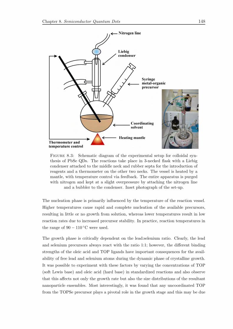
Chapter 8. Semiconductor Quantum Dots 148
Figure 8.3: Schematic diagram of the experimental setup for colloidal syn-thesis of PbSe QDs. The reactions take place in 3-necked flask with a Liebigcondenser attached to the middle neck and rubber septa for the introduction ofreagents and a thermometer on the other two necks. The vessel is heated by amantle, with temperature control via feedback. The entire apparatus is purgedwith nitrogen and kept at a slight overpressure by attaching the nitrogen line
and a bubbler to the condenser. Inset photograph of the set-up.
The nucleation phase is primarily influenced by the temperature of the reaction vessel.
Higher temperatures cause rapid and complete nucleation of the available precursors,
resulting in little or no growth from solution, whereas lower temperatures result in low
reaction rates due to increased precursor stability. In practice, reaction temperatures in
the range of 90 − 110 C were used.
The growth phase is critically dependent on the lead:selenium ratio. Clearly, the lead
and selenium precursors always react with the ratio 1:1; however, the different binding
strengths of the oleic acid and TOP ligands have important consequences for the avail-
ability of free lead and selenium atoms during the dynamic phase of crystalline growth.
It was possible to experiment with these factors by varying the concentrations of TOP
(soft Lewis base) and oleic acid (hard base) in standardized reactions and also observe
that this affects not only the growth rate but also the size distributions of the resultant
nanoparticle ensembles. Most interestingly, it was found that any uncoordinated TOP
from the TOPSe precursor plays a pivotal role in the growth stage and this may be due
Chapter 8. Semiconductor Quantum Dots 149
to the premature stabilization of the surfaces of nascent nanocrystals, rather than an
issue surrounding precursor stability. Perhaps, high concentrations of TOP within the
reaction vessel may cause a high fraction of the nanocrystal surface sites to become TOP
coordinated rather than solvent coordinated, leading to a retardation of the growth rate
and a departure from the desired “size-focusing” regime [332]. This problem may be
exacerbated by the disproportionate quantities of TOPSe used in many reported meth-
ods. On a related issue, it was also found that the reaction is sensitive to the purity of
the TOP used. The rapid rates of reaction seen if freshly distilled high-purity TOP is
used are not, in fact, conducive to the effective control of particle growth. However, in
common with other alkyl phosphines, TOP will gradually oxidize to trioctylphosphine
oxide (TOPO) if exposed to air and a large concentration of TOPO can potentially build
up before any physical signs, such as the formation of solid crystals of TOPO, are no-
ticeable. An ideal TOPO impurity concentration, where reaction rates and control over
growth are optimal, is often seen some days or weeks after distillation of the TOP and
the commercially available tech-grade TOP often produces satisfactory results. This
synthesis does not appear to yield any useful product if the TOPO impurity content
is subsequently allowed to increase still further over time. The effects of the ripening
phase should be an increase in nanocrystal size, with a corresponding red shift in the
relevant spectral peaks, as smaller particles coalesce (Ostwald ripening [334]). However,
the ripening stage is difficult to isolate and in this context is effectively subsumed into
the growth phase.
When the required nanocrystal size is reached, the reaction may be terminated by re-
moval of the heat and the addition of a large excess of methanol into the vessel. The re-
action product samples were treated by centrifuging (∼ 5000 rev/min), which facilitated
precipitation of the brown/black quantum dots. The methanol solution was decanted
away and the product dried under a stream of nitrogen. The resultant oleic acid capped
PbSe nanocrystals were stored under nitrogen and wrapped in aluminium foil until re-
quired. Subsequent spectroscopic analysis was carried out using samples dispersed into
hexanes. The longevity of PbSe stored dissolved in hexane, or any other solvent, was
not explored, however, we note that commercially available material is routinely stored
and delivered in hexane.
8.3 Optical Characterisation of Semiconductor
Nanocrystals
The absorption and photoluminescence (PL) spectra of PbSe QDs of different sizes
were experimentally obtained. The growth temperature was 100C. The absorption

Chapter 8. Semiconductor Quantum Dots 150
spectra of solutions of QDs in hexane were taken using a Hewlett Packard dual-beam
ultraviolet/visible/near-infrared spectrometer and using a hexane-only reference cell.
The optical transmittance of light through samples is measured, after reference correc-
tion, as a function of wavelength. The absorbance,A, can be calculated as a function of
wavelength by
I
I0= 10−A , (8.2)
where I is the intensity through the sample at a particular wavelength. I0 is the intensity
through the reference hexane cell.
1000 1200 1400 1600 1800 20000
0.2
0.4
0.6
0.8
wavelength
abso
rptio
n (a
.u.)
2 min4 min6 min8 min10 min
Figure 8.4: The above graphs display the absorption of PbSe quantum dotsfrom a representative synthesis for different growth times from 2 to 10 minutes,after injection. The plots show the absorption peak tuning as the particle size(time) increases. The broadening of the absorption peak is mainly related to
inhomogeneous size distribution.
As expected from quantum confinement effects, Figure 8.4 shows the absorption shift
towards the blue of the bulk band gap of 0.28 eV (4.42µm), locating the absorption
spectra in IR telecommunications wavelengths. Also, the spectra show the principal
transition (1S(h)−1S(e)) absorption peak of the PbSe nanocrystals which is size tuned
from λ = 1200nm to 1600nm between 2 and 10 min after injection. This demonstrate
how the principal absorption peak may be effectively tuned across the ∼ 1.3 − 1.55µm
telecommunications window wavelengths, and thus allows for the use of these QDs in a

Chapter 8. Semiconductor Quantum Dots 151
number of potential applications. The second exciton absorption peak (1P(h)− 1S(e))
can also be seen at shorter wavelengths in some of the larger QDs absorption spectra.
The relatively large electron, hole and exciton Bohr radii of PbSe (∼ 23, 23 and 46 nm
respectively) allows strong quantum confinement effects in relatively large structures
and a very wide range of absorption wavelengths, from the visible up to around 4µm,
that may be sampled by tuning the particle size in the 1 − 40 nm regime.
Figure 8.5: A two-level effective-mass model, predicting the variation inabsorption peak wavelength with nanocrystal diameter, for spherical PbSenanoparticles (see Appendix A). The parameters used in this model wereEg = 0.28 eV, m∗(e) = 0.084m and m∗(h) = 0.70m, where Eg is the bulkband-gap energy and m is the electron rest mass. The inset shows a schematic
band diagram for the 1S(e) and 1S(h) states of the PbSe quantum dot.
In order to correlate the absorption features of the experimental data with the par-
ticle size, an effective-mass model of the 1S(h) and 1S(e) band transitions has been
developed for spherical particles of PbSe nanoparticles [335]. This model considers a
semiconductor sphere with diameter (D) surrounded by an infinitely high potential bar-
rier, and by using appropriate values for the conduction-electron and valence-electron
effective masses and taking the bulk band-gap energy of PbSe to be 0.28 eV, the shift in
energy of the 1S levels can be calculated, as shown in Appendix A. The spacing between
the 1S(e) and 1S(h) levels then defines the band-gap energy of the PbSe nanocrystal.
Figure 8.5 shows the predicted band-gap energy as funtion of the particle diameter. This
indicates that principal absorption wavelengths are expected to vary as the particle di-
ameter changes and that diameters in the approximate range 7.7−8.5 nm are requires to
access the telecommunication-window wavelengths. Relating the absorption spectra in
Figure 8.4 to the particle in a box model indicates that the mean particle diameter was

Chapter 8. Semiconductor Quantum Dots 152
tuned from ∼ 7.3 nm through to ∼ 9.4 nm in that particular synthesis. Again by apply-
ing the particle-in-a-box model, the absorption peak broadening observed in Figure 8.4
can be related to an inhomogeneous particle size distribution. For example, in Figure
8.4 for the 4min nanocrystals, the observed full width at half-maximum of the peak is
∆λ ≈ 146 nm, the exciton absorption peak is centred at λ ≈ 1460 nm and the mean
diameter D is calculated to be D = 8.32 nm. Assuming a Gaussian size distribution and
the FWHM gives a ∆D of 0.54 nm which implies a ∆D/D, size distribution of 6.5%.
Therefore, it can be inferred that the colloidal synthesis used for the fabrication of the
QDs yields a particle size distribution of approximately 5-10% [336].
Figure 8.6: Normalized room-temperature photoluminescence spectra of PbSequantum dots from a representative synthesis for different growth times 3, 5,7 and 9 minutes after injection. The plots clearly show the size tuning of thePL peak with increased growth time. The QDs sizes were calculated by theparabolic bands and effective mass approximation, using the position of theabsorption peak obtained in each experiment [335]. The diameter was calculatedto be D = 8.07 nm, D = 8.4 nm, D = 8.45 nm and D = 8.46 nm, respectively.The broadening of the features is due to larger size distribution as the synthesistime increases. The graph also shows the absorption of the 3 min QDs for
reference (blue line).
In order to investigate the room temperature photoluminescent properties of the PbSe
quantum dots, solutions of the samples in hexanes were placed into fluorimetry-grade
silica cuvettes and excited with a λ = 808nm pulsed laser diode. The photoluminescence
was collected at a right angle to the excitation and was analyzed using a standard
collimation and monochromator arrangement and an infrared detector, with lock-in
amplification. Figure 8.6 shows typical PL spectra of different diameters PbSe quantum
Chapter 8. Semiconductor Quantum Dots 153
dots. Growth times of 3, 5, 7, 9 minutes after injection were used to tune the nanocrystal
size. In common with previous reports in the literature, the PL is somewhat (∼ 40meV)
Stokes shifted from the absorption peak, owing to a fine-structure splitting of hole states,
that is not accounted for in the simple effective-mass model described in Appendix A
[337], the absorption of the 3min quantum dots is also plot in the figure as reference. The
spectral bandwidth of the luminescence is comparable to that of the absorption peaks,
which suggests that the bandwidth is a consequence of the particle-size distribution.
The ability to size-tune the absorption features of the PbSe nanocrystals across the
telecommunications window also implies that it is possible to size-tune the PL in a
similar fashion, as shown in Figure 8.6.
Of particular importance to the use of these materials in future applications is the issue
of achieving high quantum yields (or PL efficiency) and the ability to measure and
calculate this accurately. A technique of quantitative comparison between the QDs PL
and that from an infrared dye of known quantum yield was used to accurately calculate
the sample PL efficiency. The commercially available dye used was ‘indocyanine green’
which has a 12% quantum yield in dimethylsulphoxide (DMSO). For this trial, the optical
densities of the sample and reference solutions were matched as closely as possible at the
wavelength of the diode laser excitation source (808 nm), with both solutions placed into
fluorimetry cuvettes of identical geometries and path lengths. Care was taken not to
exceed an optical density of 0.1 in either cuvette, as this might lead to problems of self-
absorption. Next, their PL was detected using the same detection set-up as described
above. The geometries and circumstances of excitation and detection were therefore
identical for sample and reference. Lastly, the PL spectra were compared in order to
calculate an accurate PL efficiency for the PbSe nanocrystal sample. Using the definition
of quantum yield
QY =Number of photons emitted
Number of photons absorbed(8.3)
and by considering both the photon energy and the sensitivity response of the detector
as functions of wavelength, it is possible to establish an accurate relation between the
two PL irradiance spectra with the known dye PL efficiency. In order to determine the
QDs quantum yield, the formula used in all PL efficiency calculations was
QY =η
∫
λIsample(λ)R(λ)dλ∫
λIref (λ)R(λ)dλ, (8.4)
where Isample and Iref are the irradiance spectra of the PL of the quantum dot and
reference dye respectively, R(λ) is the detector response function and η is the nominal
quantum yield of the reference dye.

Chapter 8. Semiconductor Quantum Dots 154
Figure 8.7: Absorption and photoluminescence spectra of the cyanine dye,indocyanine green in DMSO are shown together with the PL spectrum of a rep-resentative synthesis of PbSe nanocrystals. In order to make a correct “photonsout-photons in” calculation of the PL quantum yields, the areas under the twoPL spectra was calculate and the variations in detector response and photon
energy with wavelength was taken into account.
Figure 8.7 shows the spectra from an experiment to determine the PL efficiency of a
typical PbSe sample. The measured quantum efficiencies were as high as 60%, which
compares favorably with other reported values [333]. Table 8.1 displays values of PL
efficiency as a function of growth time (particle size). The results show a clear trend
of the efficiency decreasing at longer growth times. This effect may be due to extrin-
sic factors during the fabrication process, such as the residual presence of moisture or
oxidizing agents in the reaction vessel during the dynamic phase of crystal growth. Al-
ternatively, variations in luminescence, “blinking” effects, due to size-dependent Auger
recombination effects, as commonly seen in quantum-dot systems [338], may also play a
role.
Growth time (min) PL efficiency(%)
3 615 367 279 23
Table 8.1: Variation of the measured PL efficiency of PbSe as a function ofthe growth time.
Chapter 8. Semiconductor Quantum Dots 155
Table 8.1 shows that the photoluminescence quantum yields at room temperature ranges
between 23 and 61% and it is important to note that no inorganic surface passivation,
such as capping with a semiconductor shell was required to obtain these high quantum
efficiencies. The high quantum efficiencies observed in these experiments, combined
with the high PL stability and photon energy tuneability of PbSe nanocrystals, open
up the possibility to consider the inclusion of PbSe QDs within holey fibres as an active
medium. To achieve this it is necessary to investigate the PL properties of the QDs
when they are forming solid compounds. It should be considered that, although high
PL efficiencies in solution have been observed, such values are not likely from solid films
of the nanocrystals. This is due to the much smaller distances between nanocrystals
in such films relative to solutions and, hence, the much higher probability of energy
transfer of excitons between particles [339] and the increased likelihood of sampling a
non-radiative centre or “trap” in the structure.
In conclusion, these experiments reveal that colloidal PbSe QDs synthesized following
the method described here exhibit excellent properties: their emission can be tuned over
1.2−2µm, they can be made to be very monodisperse and offer high photoluminescence
quantum yields. By coating the inner surface of large diameter capillaries (> 75µm
in diameter), solution processed nanocrystal fibre structures have already demonstrated
optical gain and lasing in a whispering gallery mode configuration [340, 341]. Future
work will focus on the deposition of PbSe nanocrystals inside MOFs in order to add
semiconductor functionalities to MOFs. For example, fibre laser devices will be fabri-
cated by coating the inner wall of a capillary with a thin film of nanocrystals and by
filling the core with a high index fluid to guide the excitation and emission light. Feed-
back to induce lasing will be achieved by incorporating the PbSe quantum dot modified
fibre into a loop.

Chapter 9
Conclusions
In this thesis MOF have been successfully used as microfluidic vessels for the synthesis
of materials within the fibre voids, by means of high-pressure chemical deposition tech-
niques. Two main techniques, high-pressure CVD and supercritical fluid deposition were
explored as potential routes towards the fabrication of hybrid fibre devices combining
semiconductors, metals and dielectrics.
9.1 Summary of Results
This research has identified different experimental conditions for the conformal deposi-
tion of amorphous and polycrystalline silicon and germanium films. It was found that in
order to obtain conformal deposition inside high aspect ratio capillary voids of MOFs,
the semiconductor must be deposited at low temperatures, in the amorphous phase, and
crystallization is then achieved by means of a post-deposition annealing process. The
resulting silicon and germanium structures were thoroughly characterised with SEM,
TEM and Raman studies, as well as by electrical transport and optical transmission
measurements. When it was necessary to have access to the semiconductor material
itself, HF etching was used to release the semiconductor wires and tubes from the MOF
silica template. These free standing structures are the highest aspect ratio semiconduc-
tor wires/tubes fabricated to date by any known method.
SEM analysis showed that, by means of our HPCVD process, conformal tubes with
uniform internal diameter are formed over centimetre lengths inside the capillary holes
of MOFs. Capillary holes ranging from hundreds of nanometres to tens of microns in
diameter can be either partially or completely filled with silicon and germanium.
156
Chapter 9. Semiconductor Quantum Dots 157
TEM was used to extract qualitative information regarding the material structure and
the crystallite size. TEM analysis shows that germanium wires grown at 500 C are
polycrystalline with crystallite sizes of the order of 500 nm in diameter. In contrast,
the diffraction pattern of silicon wires grown at 700 C, are featureless with broad rings
and diffuse spots which implies that the material is polycrystalline, with amorphous and
small crystallite phases.
The evolution of the structural composition of silicon tubes, grown at different processing
temperatures, was studied using Raman spectroscopy. It was found that the material
goes through many phases before reaching a polycrystalline structure. At low deposition
temperatures (450 C), the material produced is amorphous and its Raman spectrum
shows a broad peak located at ∼ 480 cm−1. As the deposition temperature is increased
to 700 C, the material starts to crystallize and small crystallites are formed. Three
Voigt peaks were used to decouple the spectra and to calculate the crystallinity fraction
of the material, which was calculated to be ∼ 37%. At higher temperatures (750 C), the
crystallites grow and polycrystalline silicon with fewer defective and amorphous regions
is obtained. The crystallinity fraction of silicon tubes deposited at this temperature is
∼ 87%. Subsequently, with an annealing process at 1450 C larger crystals are formed
and the crystallinity fraction of these tubes is ∼ 100%.
In comparison, the Raman spectra of germanium tubes shows that polycrystalline ma-
terial with a crystallinity fraction of ∼ 100% is deposited at much lower temperatures
(500 C). In addition, the results of the Raman study show that in-fibre silicon tubes are
subject to tensile strain which is reflected as a redshift of the Raman peak of ∼ 2 cm−1.
Once the tubes are etched out of the MOF template the strain is released. This suggest
that it is possible to design fibre geometries to induce strain in semiconductors that may
lead to desirable changes in the electronic and optical properties of the material. Further
studies will focus on introducing additional stress during deposition either longitudinally,
by compressing or stretching, or radially, by twisting or bending the fibres.
In-fibre silicon and germanium wires were configured as FETs. These transistors are the
first example of in-fibre electronic devices and established the potential of this technology
to create an new class of optical fibres with both photonic and electronic capabilities. In
addition, in-fibre FETs served as valuable characterisation tools which provided infor-
mation about the carrier type, carrier concentration and mobility of the semiconductor
material. The carrier mobility of germanium tubes was one order of magnitude better
than that of silicon. This can be attributed to the difference in the crystalline struc-
ture between silicon and germanium tubes. Therefore, results of Raman, TEM and
electrical studies indicate that optimization of the annealing process should allow for a
reduction of the amount of amorphous and defective material along with larger grain
sizes. Higher crystallinity fraction and larger crystals should reduce the magnitude of
Chapter 9. Semiconductor Quantum Dots 158
the grain-boundary scattering in semiconductor modified MOFs and will improve their
electronic and optical properties.
This thesis has also characterised the light guiding properties of silicon-filled MOFs. The
transmission loss of a silicon fibre was measured to be ∼ 7 dB/cm at λ = 1550nm, which
is comparable to the value of 3 − 7 dB/cm reported for poly-silicon planar waveguides.
Scattering due to sidewall roughness is a critical component of the loss in planar silicon
waveguides because of the high index contrast between the core and the cladding. In-
fibre tubes/wires are fabricated inside a very smooth template, which should make their
outer diameter also very smooth. Scattering at the inner surface becomes relatively
unimportant because its area is so small as the silicon tube grows inwards. We can
conclude that the measured loss of poly-silicon fibres is mainly due to intrinsic absorption
and grain boundary scattering, and therefore further improvements on the material
quality will result in better waveguides. Work was then conducted to demonstrate
an in-fibre optical modulator based on a silicon-filled MOF. Photoexcitation of free
carriers was used to modulate light with light. The modulation concept relies on the
fact that the concentration variation of free carriers modifies the absorption of silicon.
Therefore by exciting free carries with a pulsed laser, one can drive the system from a
low absorption state to a lossy state and modulate the amplitude of light guided in the
silicon core. Optical pulses of 65µJ in the control channel were sufficient to achieve a
ten fold modulation of the probe signal.
Another advantage of MOF templates is their transparency, allowing for structuring of
the deposition within them via photolysis. Laser-assisted supercritical fluid deposition
was used to deposited gold seeds at specific locations inside the fibre. Then, single crystal
silicon wires were successfully formed via a high-pressure version of vapour-liquid-solid
growth.
Supercritical fluid deposition was employed for the deposition of metals and polymers
inside MOFs. This thesis has investigated the optical transmission properties of MOFs
with silver-nanoparticle inclusions with a range of deposition profiles. These fibres ex-
hibit low optical loss (∼ 2 dB/cm), compared to planar plasmon waveguides at visible
wavelengths. The extended interaction over centimetre lengths that is associated with
the guided core modes, makes possible the excitation of plasmon resonances on various
particle sizes, interparticle separations and film thicknesses along the fibre which resulted
in a broad absorption band across the red end of the visible spectrum. The low opti-
cal losses that were measured when visible light is guided in the core, demonstrate the
potential for the silver impregnated MOFs to be integrated with conventional photonic
devices. The ability to control the loss at longer or at specific wavelengths simply via the
metal deposition profile and the choice of MOF designs is currently under investigation.

Chapter 9. Semiconductor Quantum Dots 159
Silver-modified MOFs have been characterised using Raman measurements, demonstrat-
ing SERS detection of a single molecular layer of target molecules. The SERS data
obtained, when light is coupled into the fibre at different positions (core and cladding),
has been extremely useful for understanding the SERS process in fibre-based substrates.
A qualitative explanation of the interaction between the optical modes and the metal
nanoparticles has identified two excitation mechanisms.
In the first regime, when the pump laser is coupled into the fibre core, guided modes
are excited and can propagate over centimetre lengths (due to their relatively low loss).
During the interaction between guided modes and the silver particles near the core,
SERS photons are excited and may be efficiently collected by the high refractive index
core. As guided modes concentrate most of their energy in the core, in this mechanism
the excitation efficiency of Raman photons per until length is considered low.
The second mechanism is relevant when light is launched onto the structured cladding
and lossy modes are excited. Cladding modes highly interact with the metal particles
then exciting plasmon modes in more silver particles. The excitation efficiency per unit
length is greater than in the first case. However cladding modes’ propagation is restricted
to shorter lengths and the collection of SERS photons is less efficient than in the first
mechanism.
The ability to engineer the fibre geometry gives us the unique opportunity to control
photon/plasmon interactions via these two excitation mechanisms which can result in
fibres with large SERS enhancements. Finally, MOF SERS substrates have exceptional
temporal and mechanical stability, providing strong signals at least one year after fabri-
cation. While, in contrast, planar SERS substrates may provide enhancements for about
one month and must be handled with extreme care to avoid damaging the active area.
9.2 Future Devices and Work
Many possible active and passive devices in which the transport, generation, modula-
tion, processing and detection of light is fully integrated into optical fibres can now be
envisioned. The performance of such devices will depend critically on the quality and
crystalline structure of the materials within the fibre. Thus, as presented here, suc-
cessful realisation of these devices will rely on further improvements in the deposition
methods and the ability to deposit semiconductors in any crystalline phase. Deposition
of direct bandgap semiconductors, such as GaAs and ZnSe whose non-centrosymmetry
yields electrooptical effects, is a major step forward for in-fibre lasers and modulators.
Experiments are currently underway to improve the properties of silicon and germa-
nium structures as well as to demonstrate compound and direct bandgap semiconductor
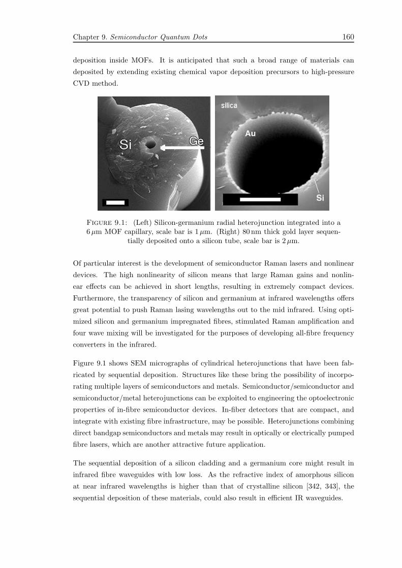
Chapter 9. Semiconductor Quantum Dots 160
deposition inside MOFs. It is anticipated that such a broad range of materials can
deposited by extending existing chemical vapor deposition precursors to high-pressure
CVD method.
Figure 9.1: (Left) Silicon-germanium radial heterojunction integrated into a6µm MOF capillary, scale bar is 1µm. (Right) 80 nm thick gold layer sequen-
tially deposited onto a silicon tube, scale bar is 2µm.
Of particular interest is the development of semiconductor Raman lasers and nonlinear
devices. The high nonlinearity of silicon means that large Raman gains and nonlin-
ear effects can be achieved in short lengths, resulting in extremely compact devices.
Furthermore, the transparency of silicon and germanium at infrared wavelengths offers
great potential to push Raman lasing wavelengths out to the mid infrared. Using opti-
mized silicon and germanium impregnated fibres, stimulated Raman amplification and
four wave mixing will be investigated for the purposes of developing all-fibre frequency
converters in the infrared.
Figure 9.1 shows SEM micrographs of cylindrical heterojunctions that have been fab-
ricated by sequential deposition. Structures like these bring the possibility of incorpo-
rating multiple layers of semiconductors and metals. Semiconductor/semiconductor and
semiconductor/metal heterojunctions can be exploited to engineering the optoelectronic
properties of in-fibre semiconductor devices. In-fiber detectors that are compact, and
integrate with existing fibre infrastructure, may be possible. Heterojunctions combining
direct bandgap semiconductors and metals may result in optically or electrically pumped
fibre lasers, which are another attractive future application.
The sequential deposition of a silicon cladding and a germanium core might result in
infrared fibre waveguides with low loss. As the refractive index of amorphous silicon
at near infrared wavelengths is higher than that of crystalline silicon [342, 343], the
sequential deposition of these materials, could also result in efficient IR waveguides.

Chapter 9. Semiconductor Quantum Dots 161
Silicon and germanium fibre FETs are a starting point for future work. The electrical
properties of high temperature annealed wires and heterojunctions are currently under
investigation. Doping strategies for p-n heterojunctions is also a major target of the
ongoing research.
There has been an increasing theoretical interest in MOFs that incorporate metallic
thin films and nanoparticles, to yield a new kind of in-fibre plasmonic devices with
applications in sensors, subwavelength optics and plasmon physics [14, 289, 290, 344, 291,
344, 345, 346]. An experimental demonstration of these theoretical predictions is another
major target of the current research. Currently investigation of the optical properties
of silver and gold impregnated MOFs, with coating profiles ranging from smooth thin
films to granular films is being carried out. The applicability of smooth coating as
resonant plasmon structures for bio/chemical sensors has been planned as future work.
Although investigation of the optical properties of fibres with metal nanoparticles has
been presented in this thesis, more detailed optical studies will be carried out in the
near future.
Finally, the ability to integrate plasmonic materials such as silver and gold within MOF
templates makes it possible to use these fibre devices for remote SERS sensing. Remote
SERS sensors is another exciting future application of metal-modified MOFs, which is
again currently under investigation.
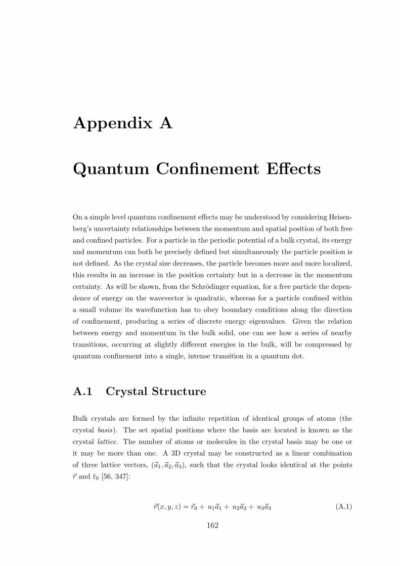
Appendix A
Quantum Confinement Effects
On a simple level quantum confinement effects may be understood by considering Heisen-
berg’s uncertainty relationships between the momentum and spatial position of both free
and confined particles. For a particle in the periodic potential of a bulk crystal, its energy
and momentum can both be precisely defined but simultaneously the particle position is
not defined. As the crystal size decreases, the particle becomes more and more localized,
this results in an increase in the position certainty but in a decrease in the momentum
certainty. As will be shown, from the Schrodinger equation, for a free particle the depen-
dence of energy on the wavevector is quadratic, whereas for a particle confined within
a small volume its wavefunction has to obey boundary conditions along the direction
of confinement, producing a series of discrete energy eigenvalues. Given the relation
between energy and momentum in the bulk solid, one can see how a series of nearby
transitions, occurring at slightly different energies in the bulk, will be compressed by
quantum confinement into a single, intense transition in a quantum dot.
A.1 Crystal Structure
Bulk crystals are formed by the infinite repetition of identical groups of atoms (the
crystal basis). The set spatial positions where the basis are located is known as the
crystal lattice. The number of atoms or molecules in the crystal basis may be one or
it may be more than one. A 3D crystal may be constructed as a linear combination
of three lattice vectors, (~a1,~a2,~a3), such that the crystal looks identical at the points
~r and r0 [56, 347]:
~r(x, y, z) = ~r0 + u1~a1 + u2~a2 + u3~a3 (A.1)
162
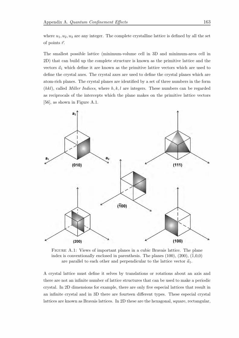
Appendix A. Quantum Confinement Effects 163
where u1, u2, u3 are any integer. The complete crystalline lattice is defined by all the set
of points ~r.
The smallest possible lattice (minimum-volume cell in 3D and minimum-area cell in
2D) that can build up the complete structure is known as the primitive lattice and the
vectors ~a1 which define it are known as the primitive lattice vectors which are used to
define the crystal axes. The crystal axes are used to define the crystal planes which are
atom-rich planes. The crystal planes are identified by a set of three numbers in the form
(hkl), called Miller Indices, where h, k, l are integers. These numbers can be regarded
as reciprocals of the intercepts which the plane makes on the primitive lattice vectors
[56], as shown in Figure A.1.
Figure A.1: Views of important planes in a cubic Bravais lattice. The planeindex is conventionally enclosed in parenthesis. The planes (100), (200), (1,0,0)
are parallel to each other and perpendicular to the lattice vector ~a1.
A crystal lattice must define it selves by translations or rotations about an axis and
there are not an infinite number of lattice structures that can be used to make a periodic
crystal. In 2D dimensions for example, there are only five especial lattices that result in
an infinite crystal and in 3D there are fourteen different types. These especial crystal
lattices are known as Bravais lattices. In 2D these are the hexagonal, square, rectangular,
Appendix A. Quantum Confinement Effects 164
centered rectangular and oblique lattices. In 3D the 14 Bravais lattices are grouped in
seven types of primitive cells, which are cubic, tetragonal, trigonal, hexagonal, triclinic,
monoclinic and orthorhombic. Some of these have more than one lattice; for example
the cubic system presents three Bravais lattices: simple cubic (SC), body-centered cubic
(BCC), and the face-centered cubic (FCC) lattices.
The crystal structure of diamond is equivalent to a face-centred cubic lattice, with a
primitive basis of two identical carbon atoms: one at ~r = (0, 0, 0) and the other at
~r = (1/4, 1/4, 1/4), where the coordinates are given as fractions along the cube sides.
This is the same as two interpenetrating FCC lattices, offset from one another along
a body diagonal by one-quarter of its length. Each atom in the diamond lattice has a
covalent bond with four adjacent atoms which together form a tetrahedron. The diamond
structure is the crystalline structure of silicon and germanium and other technological
important semiconductors. The diamond structure is formed by covalent bonding formed
in group IV materials, carbon, silicon, germanium and tin.
Figure A.2: 3D views of the crystal structure of silicon from two differentangles. The image on the right also show the atomic bonds. The lattice constantof silicon is 5.43 A which is the distance between the atoms located in the cubevertices (white lines). The blue lines correspond to 2.35 A, from reference [348].
A.2 Electron Diffraction by Crystals
In TEM analysis the crystal structure of materials is studied through the diffraction
of electrons. When and electrons waves interact with a solid they are scattered by the
crystal atoms. The resulting diffraction pattern is used to determine the crystalline
structure of the material, its lattice constants, orientation, etc. Fourier analysis tell us
that the diffraction pattern from a periodic structure can be expressed in terms of the
Fourier transform of the crystal lattice which is known as the reciprocal lattice. The
reciprocal lattice is also a Bravais lattice in the Fourier space and may be build up by

Appendix A. Quantum Confinement Effects 165
a set of primitive vectors known as the reciprocal lattice vectors, ~b1, ~b2, ~b3, which are
defined as follows [56]:
~b1 = 2π~a2 × ~a3
~a1 · ~a2 × ~a3, ~b2 = 2π
~a3 × ~a1
~a1 · ~a2 × ~a3, ~b3 = 2π
~a1 × ~a2
~a1 · ~a2 × ~a3. (A.2)
Any point in the reciprocal lattice can expressed as a linear combination of the primitive
reciprocal vectors,
~G = v1~b1 + v2~b2 + v3~b3 . (A.3)
The Brillouin zone is defined as the primitive cell in the reciprocal lattice. All the
concepts studied this appendix can be extended to photonic crystals with the only
difference being the scale of the periodic structure. In solid state crystals the distance
between atoms is a few Angstroms whereas in photonic crystals the distance between
regions with varying refractive index is of the order of the wavelength of light.
A.3 Quantum Confinement Effects
In bulk crystalline solids, the arrangement of atoms causes a periodic potential barrier
to the electron and holes motion. The electron and hole states allowed within the crystal
may be obtained by solving the stationary Schrodinger equation of a particle moving in
a periodic potential,
[
− ~2
2m∇2 + V (~r)
]
Ψ(~r) = EΨ(~r) , (A.4)
where m is the effective mass of the particle. The potential U(~r) has the periodicity of
the crystal’s Bravais lattice
V (~r) = V (~r + ~R) , (A.5)
for all lattice vectors ~R. According to Bloch’s theorem, the eigenvectors of equation A.4,
the electronic wave functions in a bulk crystal can be written as
Ψνk(~r) = uνk(~r)ei~k·~r , (A.6)
Appendix A. Quantum Confinement Effects 166
and
uνk(~r) = uνk(~r + ~R) , (A.7)
where ~k is the wave vector reduced to the first Brillouin zone and ν is the band index
(conduction or valence band). The allowed energy levels of the electron carriers are
distributed into bands with a finite energy bandgap (Eg) between the valence and con-
duction bands. In parabolic band approximation the energy eigenvalues for the electron
and hole are then given by
Ee(k) = Eg +~
2k2
2meand Eh(k) =
~2k2
2mh. (A.8)
where me and mh are the effective mass of the electron or hole respectively. In this
approximation the carriers behave as free particles with an effective mass which attempts
to incorporate the periodic potential feel by the carrier in the lattice. This approximation
allows the atoms in the lattice to be ignored and the electron and hole to be treated as
if they were free particles, but with a different mass [320].
In order to describe the consequences of quantum confinement on the allowed electron
and hole states, one can consider the particle-in-a-box model. In this model the charge
carriers with effective mass m are confined in all three dimensions inside an spherical
potential well of radius a. The confinement potential in spherical coordinate (r, θ, φ) is
given by
V =
0 for r < a
∞ for r > a(A.9)
Outside the quantum dot, the solution to the Schrodinger equation (A.4) is trivial and
gives a wavefunction equal to zero. Inside of the well (r < a), the Schrodinger equation
(A.4) takes the form
(
∇2 + k2)
Ψ(r, θ, φ) = 0 . (A.10)
where k is the wavenumber corresponding to k2 = 2mE/~ and the Laplacian in spherical
coordinates is given by
∇2 =1
r2∂
∂r2
(
r2∂
∂r2
)
+1
r2 sin θ
∂
∂θ
(
sin θ∂
∂θ
)
+1
r2 sin θ
∂2
∂φ2(A.11)
The solutions to equation (A.10) are obtained using a separation of variables approach

Appendix A. Quantum Confinement Effects 167
Ψlmn(~r) = Rln(r)Y ml (θ, φ) , (A.12)
where Y ml (θ, φ) are the spherical harmonics and the quantum numbers, n = 1, 2, 3, . . . ,
l = 0, 1, 2, . . . and m = 0,±1,±2, . . . ,±l. In addition, the spherical harmonics have the
especial property of being eigenfunctions of the Laplacian in spherical coordinates
∇2Y ml (θ, φ) =
−l(l + 1)
r2Y m
l (θ, φ) . (A.13)
The Laplacian of the product of two functions F and G is given by
∇2(FG) =(
∇2F)
G+ 2 ((∇F ) · (∇G)) + F(
∇2G)
. (A.14)
Since Rln(r) is a radial function and Y ml (θ, φ) is a spherical harmonic. The gradient of
Rln is a radial vector which is tangent to the gradient of Y ml (θ, φ), therefore
2 ((∇Rln(r)) · (∇Y ml (θ, φ)) = 0 . (A.15)
Then
∇2 (Rln(r)Y ml (θ, φ)) =
(
∇2Rln(r))
Y ml (θ, φ) +Rln(r)
(
∇2Y ml (θ, φ)
)
, (A.16)
by substitution of equation (A.13) into the previous equation,
∇2 (Rln(r)Y ml (θ, φ)) =
1
r2d
dr
(
r2dRln
dr
)
Y ml +Rln
(
−l(l + 1)
r2
)
Y ml (A.17)
The previous equation is introduced into equation (A.10) in order to separate the radial
and spherical harmonic parts. The radial part of the wavefuntion satisfies the radial
Schrodinger equation
d
drr2dRln
dr+
(
k2r2 − l(l + 1))
Rln = 0 . (A.18)
The linearly independent solutions to the radial Schrodinger equation which are regular
in the origin are given by the Bessel function of the first kind Jl. Thus, the radial
wavefunctions may be described in terms on the Bessel funtions, such that
Rln(r) = AJl(kr) , (A.19)

Appendix A. Quantum Confinement Effects 168
where A is a constant. The discrete nature of the energy levels follows from boundary
conditions imposed by the “box” which requires the radial wavefunctions to vanish at
r = a, requiring Jln(ka) = 0. This restricts the allowed k values to those where the
ka = χ ln. Where χ ln denotes the nth zero of the Bessel function of order l. The complete
solution to the spherical problem can now be expressed as,
Ψlmn(~r) = Y ml (θ, φ)Jl
(χlnr
a
)
(A.20)
The allowed energies of electrons and holes for a given values of l, n are
Eenl = Eg +
~2
2me
χ2nl
a2and Eh
nl =~
2
2mh
χ2nl
a2, (A.21)
whereEg is the bandgap energy of the respective bulk semiconductor. It can be seen from
equation (A.21) that as the semiconductor QD size decreases, the electronic excitation
shifts to higher energy; in inverse proportion to the square of the radius 1/a2. The
particle-in-a-box states may be labelled according to the principal quantum number
and symmetry, in a similar fashion to nuclear states. The four lowest lying states are
therefore, 1S(n = 0, l = 1), 1P(n = 1, l = 1), 1D(n = 1, l = 2) and 2S(n = 2, l = 0).
In a semiconductor quantum dot the electronic states are conventionally denoted as, for
example, 1S(e) and 1P(e) similarly a hole state is 1S(h).

Appendix B
List of Publications
Journal Publications
1. Transmission measurements of microstructured optical fibers with metal-
nanoparticle inclusions.
A. Amezcua-Correa, A. C. Peacock, J. Yang, P. J. A. Sazio and S. M. Howdle
In preparation.
2. Surface-enhanced Raman scattering using microstructured optical fiber
substrates.
A. Amezcua-Correa, J. Yang, A. C. Peacock, C. E. Finlayson, J. R. Hayes, P. J.
A. Sazio, J. J. Baumberg and S. M. Howdle
Advanced Functional Materials, 17, 2024, (2007).
3. Electrical and Raman characterization of silicon and germanium-filled
microstructured optical fibers.
C. E. Finlayson, A. Amezcua-Correa, P. J. A. Sazio, N. F. Baril and J. V. Badding,
Applied Physics Letters 90, 132110, (2007).
4. Microstructured optical fibers as high-pressure microfluidic reactors.
P. J. A. Sazio, A. Amezcua-Correa, C. E. Finlayson, J. R. Hayes , T. J. Schei-
demantel, N. F. Baril, B. R. Jackson, D. J. Won, F. Zhang, E. R. Margine, V.
Gopalan, V. H.Crespi and J. V. Badding,
Science 311, 1583, (2006).
5. Infrared emitting PbSe nanocrystals for telecommunication window ap-
plications.
C. E. Finlayson, A. Amezcua-Correa, P. J. A. Sazio, P. S. Walker, M. C. Grossel,
169
Appendix B. List of Publications 170
R. J. Curry, D. C. Smith and J. J. Baumberg,
Journal of Modern Optics 52, 955, (2005).
Conference Publications
1. Deposition of electronic and plasmonic materials inside microstructured
optical fibres.
A. Amezcua-Correa, A. C. Peacock, N. F. Baril, J. Calkins, D. J. Won, V. Gopalan,
J. V. Badding and P.J.A. Sazio, in Electro-Active Materials, Cranfield, 2007.
2. Electronic and plasmonic materials inside microstructured optical fi-
bres.
P. J. A. Sazio, A. Amezcua-Correa, C. E. Finlayson, J. R. Hayes , T. J. Schei-
demantel, N. F. Baril, B. R. Jackson, D. J. Won, F. Zhang, E. R. Margine, V.
Gopalan, V. H.Crespi and J. V. Badding,, in Frontiers in Optics, San Jose, 2007,
Invited Paper.
3. Highly efficient SERS inside microstructured optical fibres via optical
mode engineering.
A. C. Peacock, A. Amezcua-Correa, P. J. A. Sazio, J. J. Baumberg, J. Yang and
S. M. Howdle, in ECLEO, Munich, 2007.
4. Microstructured optical fibres as micro/nano materials templates for
optoelectronic and surface enhanced Raman scattering applications.
A. Amezcua-Correa, A. C. Peacock, C. E. Finlayson, N. F. Baril, D. J. Won, V.
Gopalan, J. V. Badding, J. Yang, S. M. Howdle, J.J. Baumberg and P. J. A. Sazio,
in Nanoscale Physics and Technology, Southampton, 2007.
5. Integrated optoelectronics in an optical fiber.
J. V. Badding, P. J. A. Sazio, V. Gopalan, A. Amezcua-Correa, T. J. Scheideman-
tel, C. E. Finlayson, N. F. Baril, B. Jackson and D. J. Won, in SPIE Photonics
West, San Jose, 2007, Invited Paper.
6. Surface enhanced Raman scattering using metal modified microstruc-
tured optical fibre substrates.
A. Amezcua-Correa, A. C. Peacock, C. E. Finlayson, J. J. Baumberg, J. Yang, S.
M. Howdle and P. J. A. Sazio, in ECOC, Cannes, 2006.
7. High Pressure CVD inside Microstructured Optical Fibres.
P. J. A. Sazio, A. Amezcua-Correa, C. E. Finlayson, J. R. Hayes, T. J. Schei-
demantel, N. F. Baril, B. R. Jackson, D. J. Won, F. Zhang, E. R. Margine, V.
Gopalan, V. H. Crespi, and J. V. Badding, in ECOC, Cannes, 2006, Invited Paper.

Appendix B. List of Publications 171
8. Surface enhanced Raman scattering using metal modified microstru-
cured optical fiber substrates.
J. Yang, A. Amezcua-Correa, A. C. Peacock,, C. E. Finlayson, J. J. Baumberg,
S. M. Howdle and P. J. A. Sazio, in Optics East: Industrial Sensing Technologies,
Boston, 2006, Invited Paper.
9. Microstructured optical fibers as high-pressure microfluidic reactors.
A. Amezcua-Correa, C. E. Finlayson, J. R. Hayes, N. F. Baril, D. J. Won, V.
Gopalan, J. V. Badding and P. J. A. Sazio, in SET for Britain, London, 2006.
10. Fabrication of extreme aspect ratio wires within photonic crystal fibers.
J. V. Badding, P. J. A. Sazio, A. Amezcua-Correa, T. J. Scheidemantel, C. E.
Finlayson, N. F. Baril, D. J. Won, H. Fang, B. Jackson, A. Borhan and V. Gopalan,
in Proceeding of SPIE, 2005.
11. Microstructured Optical Fibres Semiconductor Metamaterials.
A. Amezcua-Correa, P. J. A. Sazio, C. E. Finlayson, H. Fang, D. J. Won, T. J.
Scheidemantel, B. Jackson, N. F. Baril, V. Gopalan and J. V. Badding, in LEOS,
Sydney, 2005, Invited Paper.
12. Microstructured optical fibres semiconductor metamaterials.
A. Amezcua-Correa, C. E. Finlayson, P. J. A. Sazio, H. Fang, D. J. Won, T.
J. Scheidemantel, B. Jackson, N. F. Baril, V. Gopalan and J. V. Badding, in
PREP2005, Lancaster, 2005.
13. Microstructured optical fibres semiconductor metamaterials.
A. Amezcua-Correa, C. E. Finlayson, P. J. A. Sazio, H. Fang, D. J. Won, T. J.
Scheidemantel, B. Jackson, N. F. Baril, V. Gopalan and J. V. Badding, in ASSP,
Vienna, 2005.
14. Infrared emitting PbSe nanocrystals for telecommunication window ap-
plications.
C. E. Finlayson, A. Amezcua-Correa, R. J. Curry, P. J. A. Sazio, P. S. Walker,
M. C. Grossel, D. C. Smith and J. J. Baumberg, in ASSP, Vienna, 2005.
15. Lithography-free fabrication of high index contrast, extreme aspect ra-
tio semiconductor structures
H. Fang, D. J. Won, A. Sharan, T. J. Scheidemantel, B. Jackson, N. F. Baril,
V. Gopalan, A. Amezcua-Correa and P. J. A. Sazio, in Symposium on Infrared
Materials and Technologies, Pennsylvania, 2004, Invited Paper.
16. Lithography-free fabrication of high index contrast, extreme aspect ra-
tio semiconductor structures

Appendix B. List of Publications 172
H. Fang, D. J. Won, A. Sharan, T. J. Scheidemantel, B. Jackson, N. F. Baril, V.
Gopalan, A. Amezcua-Correa and P. J. A. Sazio, in MRS Fall Meeting, Boston,
2004.
17. Infrared emitting PbSe nanocrystals for telecommunication window ap-
plications.
C. E. Finlayson, A. Amezcua-Correa, R. J. Curry, P. J. A. Sazio, P. S. Walker,
M. C. Grossel, D. C. Smith and J. J. Baumberg, in PhotonQEP, Glasgow, 2004.

Bibliography
[1] http://www.corning.com.
[2] E. Yablonovitch. Inhibited spontaneous emission in solid-state physics and elec-
tronics. Physical Review Letters, 58(20):2059–2062, 1987.
[3] S. John. Strong localization of photons in certain disordered dielectric superlat-
tices. Physical Review Letters, 58(23):2486–2489, 1987.
[4] J. D. Joannopoulos, Robert D. Meade, and Joshua N. Winn. Photonic crystals :
molding the flow of light. Princeton University Press, Princeton, N.J., 1995.
[5] O. Painter, R. K. Lee, A. Scherer, A. Yariv, J. D. O’Brien, P. D. Dapkus,
and I. Kim. Two-dimensional photonic band-gap defect mode laser. Science,
284(5421):1819–1821, 1999.
[6] S. Y. Lin, E. Chow, V. Hietala, P. R. Villeneuve, and J. D. Joannopoulos. Ex-
perimental demonstration of guiding and bending of electromagnetic waves in a
photonic crystal. Science, 282(5387):274–276, 1998.
[7] T. Baba, N. Fukaya, and J. Yonekura. Observation of light propagation in photonic
crystal optical waveguides with bends. Electronics Letters, 35(8):654–655, 1999.
[8] T. A. Birks, P. J. Roberts, P. S. J. Russel, D. M. Atkin, and T. J. Shepherd. Full
2-D photonic bandgaps in silica/air structures. Electronics Letters, 31(22):1941–
1943, 1995.
[9] J. C. Knight, T. A. Birks, P. S. Russell, and D. M. Atkin. All-silica single-mode
optical fiber with photonic crystal cladding. Optics Letters, 21(19):1547–1549,
1996.
[10] T. A. Birks, J. C. Knight, and P. S. Russell. Endlessly single-mode photonic
crystal fiber. Optics Letters, 22(13):961–963, 1997.
[11] J. C. Knight, J. Broeng, T. A. Birks, and P. S. J. Russel. Photonic band cap
guidance in optical fibers. Science, 282(5393):1476–1478, 1998.
173
Bibliography 174
[12] P. Russell. Photonic crystal fibers. Science, 299(5605):358–362, 2003.
[13] J. C. Knight. Photonic crystal fibres. Nature, 424(6950):847–851, 2003.
[14] P. S. J. Russell. Photonic-crystal fibers. Journal of Lightwave Technology,
24(12):4729–4749, 2006.
[15] T. M. Monro and D. J. Richardson. Holey optical fibres: Fundamental properties
and device applications. Comptes Rendus Physique, 4(1):175–186, 2003.
[16] P. J. A. Sazio, A. Amezcua-Correa, C. E. Finlayson, J. R. Hayes, T. J. Scheideman-
tel, N. F. Baril, B. R. Jackson, D. J. Won, F. Zhang, E. R. Margine, V. Gopalan,
V. H. Crespi, and J. V. Badding. Microstructured optical fibers as high-pressure
microfluidic reactors. Science, 311(5767):1583–1586, 2006.
[17] J. V. Badding, V. Copalan, and P. J. A. Sazio. Building semiconductor structures
in optical fiber. Photonics Spectra, 40(8):80–88, 2006.
[18] A. M. Morales and C. M. Lieber. A laser ablation method for the synthesis of
crystalline semiconductor nanowires. Science, 279(5348):208–211, 1998.
[19] Y. Huang, X. F. Duan, Y. Cui, L. J. Lauhon, K. H. Kim, and C. M. Lieber.
Logic gates and computation from assembled nanowire building blocks. Science,
294(5545):1313–1317, 2001.
[20] Y. Cui and C. M. Lieber. Functional nanoscale electronic devices assembled using
silicon nanowire building blocks. Science, 291(5505):851–853, 2001.
[21] X. F. Duan, Y. Huang, R. Agarwal, and C. M. Lieber. Single-nanowire electrically
driven lasers. Nature, 421(6920):241–245, 2003.
[22] R. S. Friedman, M. C. McAlpine, D. S. Ricketts, D. Ham, and C. M. Lieber.
High-speed integrated nanowire circuits. Nature, 434(7037):1085–1085, 2005.
[23] E. Yablonovitch, T. J. Gmitter, and K. M. Leung. Photonic band-structure - the
face-centered-cubic case employing nonspherical atoms. Physical Review Letters,
67(17):2295–2298, 1991.
[24] Y. A. Vlasov, K. Luterova, I. Pelant, B. Honerlage, and V. N. Astratov. Enhance-
ment of optical gain of semiconductors embedded in three-dimensional photonic
crystals. Applied Physics Letters, 71(12):1616–1618, 1997.
[25] K. Busch and S. John. Liquid-crystal photonic-band-gap materials: The tunable
electromagnetic vacuum. Physical Review Letters, 83(5):967–970, 1999.

Bibliography 175
[26] E. Yablonovitch. Optics - liquid versus photonic crystals. Nature, 401(6753):539,
1999.
[27] P. Vukusic and J. R. Sambles. Photonic structures in biology. Nature,
424(6950):852–855, 2003.
[28] S. Y. Lin, J. G. Fleming, D. L. Hetherington, B. K. Smith, R. Biswas, K. M.
Ho, M. M. Sigalas, W. Zubrzycki, S. R. Kurtz, and J. Bur. A three-dimensional
photonic crystal operating at infrared wavelengths. Nature, 394(6690):251–253,
1998.
[29] P. G. Kazansky and V. Pruneri. Electrically stimulated light-induced second-
harmonic generation in glass: Evidence of coherent photoconductivity. Physical
Review Letters, 78(15):2956–2959, 1997.
[30] M. Key, I. G. Hughes, W. Rooijakkers, B. E. Sauer, E. A. Hinds, D. J. Richardson,
and P. G. Kazansky. Propagation of cold atoms along a miniature magnetic guide.
Physical Review Letters, 84(7):1371–1373, 2000.
[31] P. S. Westbrook, B. J. Eggleton, R. S. Windeler, A. Hale, T. A. Strasser, and
G. L. Burdge. Cladding-mode resonances in hybrid polymer-silica microstructured
optical fiber gratings. IEEE Photonics Technology Letters, 12(5):495–497, 2000.
[32] C. Kerbage, A. Hale, A. Yablon, R. S. Windeler, and B. J. Eggleton. Integrated
all-fiber variable attenuator based on hybrid microstructure fiber. Applied Physics
Letters, 79(19):3191–3193, 2001.
[33] M. Fokine, L. E. Nilsson, A. Claesson, D. Berlemont, L. Kjellberg, L. Krum-
menacher, and W. Margulis. Integrated fiber Mach-Zehnder interferometer for
electro-optic switching. Optics Letters, 27(18):1643–1645, 2002.
[34] T. T. Larsen, A. Bjarklev, D. S. Hermann, and J. Broeng. Optical devices based
on liquid crystal photonic bandgap fibres. Optics Express, 11(20):2589–2596, 2003.
[35] F. Benabid, F. Couny, J. C. Knight, T. A. Birks, and P. S. Russell. Compact, stable
and efficient all-fibre gas cells using hollow-core photonic crystal fibres. Nature,
434(7032):488–491, 2005.
[36] F. Benabid, J. C. Knight, G. Antonopoulos, and P. S. J. Russell. Stimulated
Raman scattering in hydrogen-filled hollow-core photonic crystal fiber. Science,
298(5592):399–402, 2002.
[37] M. Bayindir, F. Sorin, A. F. Abouraddy, J. Viens, S. D. Hart, J. D. Joannopou-
los, and Y. Fink. Metal-insulator-semiconductor optoelectronic fibres. Nature,
431(7010):826–829, 2004.
Bibliography 176
[38] D. J. Monk and D. R. Walt. Fabrication of gold microtubes and microwires in
high aspect ratio capillary arrays. Journal of the American Chemical Society,
126(37):11416–11417, 2004.
[39] N. R. B. Coleman, M. A. Morris, T. R. Spalding, and J. D. Holmes. The formation
of dimensionally ordered silicon nanowires within mesoporous silica. Journal of
the American Chemical Society, 123(1):187–188, 2001.
[40] N. R. B. Coleman, K. M. Ryan, T. R. Spalding, J. D. Holmes, and M. A. Morris.
The formation of dimensionally ordered germanium nanowires within mesoporous
silica. Chemical Physics Letters, 343(1-2):1–6, 2001.
[41] D. P. Long, J. M. Blackburn, and J. J. Watkins. Chemical fluid deposition: A hy-
brid technique for low-temperature metallization. Advanced Materials, 12(12):913–
915, 2000.
[42] J. M. Blackburn, D. P. Long, A. Cabanas, and J. J. Watkins. Deposition of
conformal copper and nickel films from supercritical carbon dioxide. Science,
294(5540):141–145, 2001.
[43] J. J. Watkins, J. M. Blackburn, and T. J. McCarthy. Chemical fluid deposition:
Reactive deposition of platinum metal from carbon dioxide solution. Chemistry of
Materials, 11(2):213–215, 1999.
[44] C. R. Kurkjian, J. T. Krause, and M. J. Matthewson. Strength and fatigue of
silica optical fibers. Journal of Lightwave Technology, 7(9):1360–1370, 1989.
[45] P. Kaiser, E. A. J. Marcatili, and S.E. Miller. A new optical fiber. Bell System
and Technical Journal, 52(2):265–269, 1973.
[46] P. Kaiser and H. W. Astle. Low-loss single material fibers made from pure fused
silica. Bell System and Technical Journal, 53:1021–1039, 1974.
[47] P. Yeh, A. Yariv, and E. Marom. Theory of Bragg fiber. Journal of the Optical
Society of America, 68(9):1196–1201, 1978.
[48] S. R. Nagel, J. B. Macchesney, and K. L. Walker. An overview of the modified
chemical vapor-deposition (MCVD) process and performance. IEEE Journal of
Quantum Electronics, 18(4):459–476, 1982.
[49] F. Brechet, P. Roy, J. Marcou, and D. Pagnoux. Singlemode propagation into
depressed-core-index photonic-bandgap fibre designed for zero-dispersion propa-
gation at short wavelengths. Electronics Letters, 36(6):514–515, 2000.

Bibliography 177
[50] F. Brechet, P. Leproux, P. Roy, J. Marcou, and D. Pagnoux. Analysis of band-
pass filtering behaviour of singlemode depressed-core-index photonic-bandgap fi-
bre. Electronics Letters, 36(10):870–872, 2000.
[51] B. Temelkuran, S. D. Hart, G. Benoit, J. D. Joannopoulos, and Y. Fink.
Wavelength-scalable hollow optical fibres with large photonic bandgaps for CO2
laser transmission. Nature, 420(6916):650–653, 2002.
[52] M. Ibanescu, Y. Fink, S. Fan, E. L. Thomas, and J. D. Joannopoulos. An all-
dielectric coaxial waveguide. Science, 289(5478):415–419, 2000.
[53] K. Kuriki, O. Shapira, S. D. Hart, G. Benoit, Y. Kuriki, J. F. Viens, M. Bayindir,
J. D. Joannopoulos, and Y. Fink. Hollow multilayer photonic bandgap fibers for
NIR applications. Optics Express, 12(8):1510–1517, 2004.
[54] R. F. Cregan, B. J. Mangan, J. C. Knight, T. A. Birks, P. S. Russell, P. J. Roberts,
and D. C. Allan. Single-mode photonic band gap guidance of light in air. Science,
285(5433):1537–1539, 1999.
[55] S. John. Electromagnetic absorption in a disordered medium near a photon mo-
bility edge. Physical Review Letters, 53(22):2169–2172, 1984.
[56] C. Kittel. Introduction to solid state physics. Wiley, New York, 7th edition, 1996.
[57] H. P. Myers. Introductory solid state physics. Taylor and Francis, London, 2nd
edition, 1997.
[58] G. P. Agrawal. Nonlinear fiber optics. Academic Press, San Diego, 3rd edition,
2001.
[59] S. K. Varshney, M. P. Singh, and R. K. Sinha. Propagation characteristics of
photonic crystal fibers. Journal of Optical Communications, 24, 2002.
[60] M. D. Nielsen and N. A. Mortensen. Photonic crystal fiber design based on the
V -parameter. Optics Express, 11(21):2762–2768, 2003.
[61] J. C. Knight, T. A. Birks, R. F. Cregan, P. S. Russell, and J. P. de Sandro. Large
mode area photonic crystal fibre. Electronics Letters, 34(13):1347–1348, 1998.
[62] T. M. Monro, D. J. Richardson, N. G. R. Broderick, and P. J. Bennett. Ho-
ley optical fibers: An efficient modal model. Journal of Lightwave Technology,
17(6):1093–1102, 1999.
[63] N. A. Mortensen, M. D. Nielsen, J. R. Folkenberg, A. Petersson, and H. R. Si-
monsen. Improved large-mode-area endlessly single-mode photonic crystal fibers.
Optics Letters, 28(6):393–395, 2003.

Bibliography 178
[64] K. Furusawa, T. M. Monro, P. Petropoulos, and D. J. Richardson. Modelocked
laser based on ytterbium doped holey fibre. Electronics Letters, 37(9):560–561,
2001.
[65] J. Limpert, T. Schreiber, S. Nolte, H. Zellmer, A. Tunnermann, R. Iliew, F. Led-
erer, J. Broeng, G. Vienne, A. Petersson, and C. Jakobsen. High-power air-clad
large-mode-area photonic crystal fiber laser. Optics Express, 11(7):818–823, 2003.
[66] W. J. Wadsworth, R. M. Percival, G. Bouwmans, J. C. Knight, and P. S. J. Russel.
High power air-clad photonic crystal fibre laser. Optics Express, 11(1):48–53, 2003.
[67] N. G. R. Broderick, T. M. Monro, P. J. Bennett, and D. J. Richardson. Nonlinear-
ity in holey optical fibers: measurement and future opportunities. Optics Letters,
24(20):1395–1397, 1999.
[68] J. C. Knight, J. Arriaga, T. A. Birks, A. Ortigosa-Blanch, W. J. Wadsworth, and
P. S. Russell. Anomalous dispersion in photonic crystal fiber. IEEE Photonics
Technology Letters, 12(7):807–809, 2000.
[69] W. H. Reeves, D. V. Skryabin, F. Biancalana, J. C. Knight, P. S. Russell, F. G.
Omenetto, A. Efimov, and A. J. Taylor. Transformation and control of ultra-short
pulses in dispersion-engineered photonic crystal fibres. Nature, 424(6948):511–515,
2003.
[70] D. Mogilevtsev, T. A. Birks, and P. S. Russell. Group-velocity dispersion in pho-
tonic crystal fibers. Optics Letters, 23(21):1662–1664, 1998.
[71] A. Ferrando, E. Silvestre, J. J. Miret, and P. Andres. Nearly zero ultraflattened
dispersion in photonic crystal fibers. Optics Letters, 25(11):790–792, 2000.
[72] W. H. Reeves, J. C. Knight, P. S. J. Russell, and P. J. Roberts. Demonstration of
ultra-flattened dispersion in photonic crystal fibers. Optics Express, 10(14):609–
613, 2002.
[73] V. Finazzi, T. M. Monro, and D. J. Richardson. Small-core silica holey fibers:
nonlinearity and confinement loss trade-offs. Journal of the Optical Society of
America B-Optical Physics, 20(7):1427–1436, 2003.
[74] P. Petropoulos, T. M. Monro, W. Belardi, K. Furusawa, J. H. Lee, and D. J.
Richardson. 2R-regenerative all-optical switch based on a highly nonlinear holey
fiber. Optics Letters, 26(16):1233–1235, 2001.
[75] J. E. Sharping, M. Fiorentino, P. Kumar, and R. S. Windeler. All-optical switch-
ing based on cross-phase modulation in microstructure fiber. IEEE Photonics
Technology Letters, 14(1):77–79, 2002.

Bibliography 179
[76] J. H. Lee, P. C. Teh, Z. Yusoff, M. Ibsen, W. Belardi, T. M. Monro, and
D. J. Richardson. A holey fiber-based nonlinear thresholding device for optical
CDMA receiver performance enhancement. IEEE Photonics Technology Letters,
14(6):876–878, 2002.
[77] Z. Yusoff, J. H. Lee, W. Belardi, T. M. Monro, P. C. Teh, and D. J. Richardson.
Raman effects in a highly nonlinear holey fiber: amplification and modulation.
Optics Letters, 27(6):424–426, 2002.
[78] J. E. Sharping, M. Fiorentino, P. Kumar, and R. S. Windeler. Optical paramet-
ric oscillator based on four-wave mixing in microstructure fiber. Optics Letters,
27(19):1675–1677, 2002.
[79] X. Liu, C. Xu, W. H. Knox, J. K. Chandalia, B. J. Eggleton, S. G. Kosinski, and
R. S. Windeler. Soliton self-frequency shift in a short tapered air-silica microstruc-
ture fiber. Optics Letters, 26(6):358–360, 2001.
[80] M. Fiorentino, J. E. Sharping, P. Kumar, A. Porzio, and R. S. Windeler. Soliton
squeezing in microstructure fiber. Optics Letters, 27(8):649–651, 2002.
[81] J. K. Ranka, R. S. Windeler, and A. J. Stentz. Visible continuum generation
in air-silica microstructure optical fibers with anomalous dispersion at 800 nm.
Optics Letters, 25(1):25–27, 2000.
[82] J. Herrmann, U. Griebner, N. Zhavoronkov, A. Husakou, D. Nickel, J. C. Knight,
W. J. Wadsworth, P. S. J. Russell, and G. Korn. Experimental evidence for
supercontinuum generation by fission of higher-order solitons in photonic fibers.
Physical Review Letters, 88(17):173901, 2002.
[83] A. V. Husakou and J. Herrmann. Supercontinuum generation of higher-order soli-
tons by fission in photonic crystal fibers. Physical Review Letters, 8720(20):203901,
2001.
[84] W. J. Wadsworth, A. Ortigosa-Blanch, J. C. Knight, T. A. Birks, T. P. M. Man,
and P. S. Russell. Supercontinuum generation in photonic crystal fibers and optical
fiber tapers: a novel light source. Journal of the Optical Society of America B-
Optical Physics, 19(9):2148–2155, 2002.
[85] S. Coen, A. H. L. Chan, R. Leonhardt, J. D. Harvey, J. C. Knight, W. J.
Wadsworth, and P. S. J. Russell. White-light supercontinuum generation with
60-ps pump pulses in a photonic crystal fiber. Optics Letters, 26(17):1356–1358,
2001.

Bibliography 180
[86] J. M. Dudley, G. Genty, and S. Coen. Supercontinuum generation in photonic
crystal fiber. Reviews of Modern Physics, 78(4):1135–1184, 2006.
[87] G. Humbert, W. J. Wadsworth, S. G. Leon-Saval, J. C. Knight, T. A. Birks,
P. S. J. Russell, M. J. Lederer, D. Kopf, K. Wiesauer, E. I. Breuer, and D. Stifter.
Supercontinuum generation system for optical coherence tomography based on
tapered photonic crystal fibre. Optics Express, 14(4):1596–1603, 2006.
[88] P. Petropoulos, H. Ebendorff-Heidepriem, V. Finazzi, R. C. Moore, K. Frampton,
D. J. Richardson, and T. M. Monro. Highly nonlinear and anomalously dispersive
lead silicate glass holey fibers. Optics Express, 11(26):3568–3573, 2003.
[89] A. V. Husakou and J. Herrmann. Supercontinuum generation in photonic crystal
fibers made from highly nonlinear glasses. Applied Physics B-Lasers and Optics,
77(2-3):227–234, 2003.
[90] A. Bjarklev, A. Sanchez Bjarklev, and J. Broeng. Photonic crystal fibres. Kluwer
Academic Publishers, Boston, 2003.
[91] M. D. Feit and J. A. Fleck. Light-propagation in graded-index optical fibers.
Applied Optics, 17(24):3990–3998, 1978.
[92] M. D. Feit and J. A. Fleck. Computation of mode properties in optical fiber
wave-guides by a propagating beam method. Applied Optics, 19(7):1154–1164,
1980.
[93] S. Jungling and J. C. Chen. A study and optimization of eigenmode calcula-
tions using the imaginary-distance beam-propagation method. IEEE Journal of
Quantum Electronics, 30(9):2098–2105, 1994.
[94] R. Scarmozzino, A. Gopinath, R. Pregla, and S. Helfert. Numerical techniques
for modeling guided-wave photonic devices. IEEE Journal of Selected Topics in
Quantum Electronics, 6(1):150–162, 2000.
[95] K. Saitoh and M. Koshiba. Full-vectorial imaginary-distance beam propagation
method based on a finite element scheme: Application to photonic crystal fibers.
IEEE Journal of Quantum Electronics, 38(7):927–933, 2002.
[96] R.T. Bise, R. S. Windeler, K.S. Kranz, B. J. Eggleton, and D.J. Trevor. Tune-
able photonic bandgap fiber. In Optical Fiber Communications, pages 466–468,
Anahaim, 2002.
[97] S. W. Leonard, H. M. van Driel, K. Busch, S. John, A. Birner, A. P. Li, F. Muller,
U. Gosele, and V. Lehmann. Attenuation of optical transmission within the band
Bibliography 181
gap of thin two-dimensional macroporous silicon photonic crystals. Applied Physics
Letters, 75(20):3063–3065, 1999.
[98] R. A. Soref and B. R. Bennett. Electrooptical effects in silicon. IEEE Journal of
Quantum Electronics, 23(1):123–129, 1987.
[99] R. Feynman. There is plenty of room at the bottom, 1959.
[100] Geoffrey A. Ozin and Andre C. Arsenault. Nanochemistry : a chemical approach
to nanomaterials. Royal Society of Chemistry, Cambridge, UK, 2005.
[101] R. Wetherbee. The diatom glasshouse. Science, 298(5593):547–547, 2002.
[102] K. H. Jeong, J. Kim, and L. P. Lee. Biologically inspired artificial compound eyes.
Science, 312(5773):557–561, 2006.
[103] R. A. Pai, R. Humayun, M. T. Schulberg, A. Sengupta, J. N. Sun, and J. J.
Watkins. Mesoporous silicates prepared using preorganized templates in super-
critical fluids. Science, 303(5657):507–510, 2004.
[104] K. P. Johnston and P. S. Shah. Materials science - making nanoscale materials
with supercritical fluids. Science, 303(5657):482–483, 2004.
[105] George E. Possin. A method for forming very small diameter wires. Review of
Scientific Instruments, 41(5):772–774, 1970.
[106] R. F. Service. Materials science - throwing-or molding-a curve into nanofabrica-
tion. Science, 273(5273):312–312, 1996.
[107] Y. N. Xia, E. Kim, X. M. Zhao, J. A. Rogers, M. Prentiss, and G. M. Whitesides.
Complex optical surfaces formed by replica molding against elastomeric masters.
Science, 273(5273):347–349, 1996.
[108] Y. A. Vlasov, X. Z. Bo, J. C. Sturm, and D. J. Norris. On-chip natural assembly
of silicon photonic bandgap crystals. Nature, 414(6861):289–293, 2001.
[109] C. R. Martin. Membrane-based synthesis of nanomaterials. Chemistry of Materi-
als, 8(8):1739–1746, 1996.
[110] T. E. Bogart, S. Dey, K. K. Lew, S. E. Mohney, and J. M. Redwing. Diameter-
controlled synthesis of silicon nanowires using nanoporous alumina membranes.
Advanced Materials, 17(1):114–117, 2005.
[111] O. D. Velev, T. A. Jede, R. F. Lobo, and A. M. Lenhoff. Porous silica via colloidal
crystallization. Nature, 389(6650):447–448, 1997.

Bibliography 182
[112] O. D. Velev, P. M. Tessier, A. M. Lenhoff, and E. W. Kaler. Materials - a class of
porous metallic nanostructures. Nature, 401(6753):548–548, 1999.
[113] S. A. Johnson, P. J. Ollivier, and T. E. Mallouk. Ordered mesoporous polymers
of tunable pore size from colloidal silica templates. Science, 283(5404):963–965,
1999.
[114] D. J. Norris and Y. A. Vlasov. Chemical approaches to three-dimensional semi-
conductor photonic crystals. Advanced Materials, 13(6):371–376, 2001.
[115] P. N. Bartlett, J. J. Baumberg, P. R. Birkin, M. A. Ghanem, and M. C. Netti.
Highly ordered macroporous gold and platinum films formed by electrochemical
deposition through templates assembled from submicron diameter monodisperse
polystyrene spheres. Chemistry of Materials, 14(5):2199–2208, 2002.
[116] S. John and K. Busch. Photonic bandgap formation and tunability in certain self-
organizing systems. Journal of Lightwave Technology, 17(11):1931–1943, 1999.
[117] G. M. Whitesides and M. Boncheva. Beyond molecules: Self-assembly of meso-
scopic and macroscopic components. Proceedings of the National Academy of Sci-
ences of the United States of America, 99(8):4769–4774, 2002.
[118] Marc J. Madou. Fundamentals of microfabrication : the science of miniaturization.
CRC Press, Boca Raton, Fla., 2nd edition, 2002.
[119] Ivor Brodie and Julius J. Muray. The physics of microfabrication. Plenum Press,
New York, 1982.
[120] N. Agarwal, N. Kane, and R. F. Bunshah. Structure and property relationships
of Ni-20Cr produced by high-rate physical vapor-deposition. Journal of Vacuum
Science and Technology, 12(2):619–623, 1975.
[121] D. H. Boone, Strangma.Te, and L. W. Wilson. Some effects of structure and com-
position on properties of electron-beam vapor-deposited coatings for gas-turbine
superalloys. Journal of Vacuum Science and Technology, 11(4):641–646, 1974.
[122] J.J. Tietjen. Chemical vapor deposition of electronic materials. Annual Review of
Materials Science, 3:317–326, 1973.
[123] W. G. French, J. B. Macchesney, and A. D. Pearson. Glass fibers for optical
communications. Annual Review of Materials Science, 5:373–394, 1975.
[124] K. L. Choy. Chemical vapour deposition of coatings. Progress in Materials Science,
48(2):57–170, 2003.

Bibliography 183
[125] M. J. Ludowise. Metalorganic chemical vapor-deposition of III-V semiconductors.
Journal of Applied Physics, 58(8):R31–R55, 1985.
[126] X. H. Hou and K. L. Choy. Processing and applications of aerosol-assisted chemical
vapor deposition. Chemical Vapor Deposition, 12(10):583–596, 2006.
[127] F. T. Wallenberger and P. C. Nordine. Strong, pure, and uniform carbon-fibers
obtained directly from the vapor-phase. Science, 260(5104):66–68, 1993.
[128] T. H. Baum and C. R. Jones. Laser chemical vapor-deposition of gold. Applied
Physics Letters, 47(5):538–540, 1985.
[129] H.M. Manasevit. Single-crystal gallium arsenide on insulating substrates. Applied
Physics Letters, 12:156–159, 1968.
[130] P. D. Dapkus. Metalorganic chemical vapor-deposition. Annual Review of Mate-
rials Science, 12:243–269, 1982.
[131] C.R. Martin. Nanomaterials: A membrane-based synthetic approach. Science,
266:1961–1966, 1994.
[132] S. A. Sapp, D. T. Mitchell, and C. R. Martin. Using template-synthesized micro-
and nanowires as building blocks for self-assembly of supramolecular architectures.
Chemistry of Materials, 11(5):1183, 1999.
[133] R. M. Penner. Mesoscopic metal particles and wires by electrodeposition. Journal
of Physical Chemistry B, 106(13):3339–3353, 2002.
[134] A. M. Kressin, V. V. Doan, J. D. Klein, and M. J. Sailor. Synthesis of stoichiomet-
ric cadmium selenide films via sequential monolayer electrodeposition. Chemistry
of Materials, 3(6):1015–1020, 1991.
[135] J. D. Klein, R. D. Herrick, D. Palmer, M. J. Sailor, C. J. Brumlik, and C. R.
Martin. Electrochemical fabrication of cadmium chalcogenide microdiode arrays.
Chemistry of Materials, 5(7):902–904, 1993.
[136] S. A. Sapp, B. B. Lakshmi, and C. R. Martin. Template synthesis of bismuth
telluride nanowires. Advanced Materials, 11(5):402–404, 1999.
[137] K. B. Jirage, J. C. Hulteen, and C. R. Martin. Nanotubule-based molecular-
filtration membranes. Science, 278(5338):655–658, 1997.
[138] J. C. Hulteen, K. B. Jirage, and C. R. Martin. Introducing chemical transport
selectivity into gold nanotubule membranes. Journal of the American Chemical
Society, 120(26):6603–6604, 1998.
Bibliography 184
[139] V. P. Menon and C. R. Martin. Fabrication and evaluation of nanoelectrode
ensembles. Analytical Chemistry, 67(13):1920–1928, 1995.
[140] A. I. Cooper. Polymer synthesis and processing using supercritical carbon dioxide.
Journal of Materials Chemistry, 10(2):207–234, 2000.
[141] Erdogan Kiran, Pablo G. Debenedetti, Cor J. Peters, and North Atlantic Treaty
Organization. Scientific Affairs Division. Supercritical fluids : fundamentals and
applications. Kluwer Academic Publishers, Dordrecht ; Boston, 2000.
[142] M. Poliakoff and S. Howdle. Supercritical chemistry - synthesis with a scanner.
Chemistry in Britain, 31(2):118–121, 1995.
[143] Brian N. Hansen, Brooks M. Hybertson, Robert M. Barkley, and Robert E. Sievers.
Supercritical fluid transport-chemical deposition of films. 4(4):749–752, 1992.
[144] A. Cabanas, D. P. Long, and J. J. Watkins. Deposition of gold films and nanostruc-
tures from supercritical carbon dioxide. Chemistry of Materials, 16(10):2028–2033,
2004.
[145] J. M. Blackburn, D. P. Long, and J. J. Watkins. Reactive deposition of conformal
palladium films from supercritical carbon dioxide solution. Chemistry of Materials,
12(9):2625–2631, 2000.
[146] N. E. Fernandes, S. M. Fisher, J. C. Poshusta, D. G. Vlachos, M. Tsapatsis, and
J. J. Watkins. Reactive deposition of metal thin films within porous supports from
supercritical fluids. Chemistry of Materials, 13(6):2023–2031, 2001.
[147] A. Cabanas, J. M. Blackburn, and J. J. Watkins. Deposition of Cu films from
supercritical fluids using cu(i) beta-diketonate precursors. Microelectronic Engi-
neering, 64(1-4):53–61, 2002.
[148] E. T. Hunde and J. J. Watkins. Reactive deposition of cobalt and nickel films
from their metallocenes in supercritical carbon dioxide solution. Chemistry of
Materials, 16(3):498–503, 2004.
[149] J. V. Badding, P. J. A. Sazio, A. Amezcua-Correa, T. J. Scheidemantel, C. E. Fin-
layson, N. F. Baril, D. J. Won, H. Fang, B. Jackson, A. Borhan, and V. Gopalan.
Fabrication of extreme aspect ratio wires within photonic crystal fibers. Proceeding
of SPIE, 2005.
[150] B. R. Jackson. Template-Directed High-Pressure Vapour-Liquid-Solid Growth of
Silicon Micro-Wires within Silica Capillary Microstructured Optical fibres. PhD
thesis, The Pennsylvania State University, 2005.

Bibliography 185
[151] R.S. Wagner and W.C. Ellis. Vapor-liquid-solid mechanism of single crystal
growth. Applied Physics Letters, 4(5):89–90, 1964.
[152] Y. Cui, Q. Q. Wei, H. K. Park, and C. M. Lieber. Nanowire nanosensors for
highly sensitive and selective detection of biological and chemical species. Science,
293(5533):1289–1292, 2001.
[153] X. F. Duan, Y. Huang, Y. Cui, J. F. Wang, and C. M. Lieber. Indium phosphide
nanowires as building blocks for nanoscale electronic and optoelectronic devices.
Nature, 409(6816):66–69, 2001.
[154] J. F. Wang, M. S. Gudiksen, X. F. Duan, Y. Cui, and C. M. Lieber. Highly
polarized photoluminescence and photodetection from single indium phosphide
nanowires. Science, 293(5534):1455–1457, 2001.
[155] J. Xiang, W. Lu, Y. J. Hu, Y. Wu, H. Yan, and C. M. Lieber. Ge/Si nanowire het-
erostructures as high-performance field-effect transistors. Nature, 441(7092):489–
493, 2006.
[156] A. San Paulo, N. Arellano, J. A. Plaza, R. R. He, C. Carraro, R. Maboudian,
R. T. Howe, J. Bokor, and P. D. Yang. Suspended mechanical structures based
on elastic silicon nanowire arrays. Nano Letters, 7(4):1100–1104, 2007.
[157] Y. N. Xia, P. D. Yang, Y. G. Sun, Y. Y. Wu, B. Mayers, B. Gates, Y. D. Yin,
F. Kim, and Y. Q. Yan. One-dimensional nanostructures: Synthesis, characteri-
zation, and applications. Advanced Materials, 15(5):353–389, 2003.
[158] B. J. Eggleton, C. Kerbage, P. S. Westbrook, R. S. Windeler, and A. Hale. Mi-
crostructured optical fiber devices. Optics Express, 9(13):698–713, 2001.
[159] Ian M. Watt. The principles and practice of electron microscopy. Cambridge
University Press, Cambridge ; New York, 2nd edition, 1997.
[160] Desmond Kay. Techniques for electron microscopy. F. A. Davis Co., Philadelphia,
2d edition, 1965.
[161] B. N. Brockhouse and P. K. Iyengar. Normal modes of germanium by neutron
spectrometry. Physical Review, 111(3):747–754, 1958.
[162] J. H. Parker, D. W. Feldman, and M. Ashkin. Raman scattering by silicon and
germanium. Physical Review, 155(3):712, 1967.
[163] E. Bustarret, M. A. Hachicha, and M. Brunel. Experimental-determination of the
nanocrystalline volume fraction in silicon thin-films from Raman-spectroscopy.
Applied Physics Letters, 52(20):1675–1677, 1988.
Bibliography 186
[164] H. Xia, Y. L. He, L. C. Wang, W. Zhang, X. N. Liu, X. K. Zhang, D. Feng,
and H. E. Jackson. Phonon mode study of Si nanocrystals using micro-Raman
spectroscopy. Journal of Applied Physics, 78(11):6705–6708, 1995.
[165] H. Touir, J. Dixmier, K. Zellama, J. F. Morhange, and P. Elkaim. Bimodal crys-
tal size distribution in annealed RF magnetron silicon films: a memory effect of
the local order inhomogeneities in the initial amorphous state. Journal of Non-
Crystalline Solids, 230:906–910, 1998.
[166] A. A. Parr, D. J. Gardiner, R. T. Carline, D. O. King, and G. M. Williams.
Structural variations in polysilicon, associated with deposition temperature and
degree of anneal. Journal of Materials Science, 36(1):207–212, 2001.
[167] S. Veprek, F. A. Sarott, and Z. Iqbal. Effect of grain boundaries on the Raman
spectra, optical absorption, and elastic light scattering in nanometer-sized crys-
talline silicon. Physical Review B, 36(6):3344–3350.
[168] A. A. Parr, K. Gill, D. J. Gardiner, J. D. Hoyland, D. Sands, K. Brunson, and
R. T. Carline. A comparison of laser- and furnace-annealed polysilicon structure.
Semiconductor Science and Technology, 17(1):47–54, 2002.
[169] M. H. Brodsky, M. Cardona, and J. J. Cuomo. Infrared and Raman-spectra
of silicon-hydrogen bonds in amorphous silicon prepared by glow-discharge and
sputtering. Physical Review B, 16(8):3556–3571, 1977.
[170] C. Das and S. Ray. Onset of microcrystallinity in silicon thin films. Thin Solid
Films, 403:81–85, 2002.
[171] T. Kaneko, M. Wakagi, K. Onisawa, and T. Minemura. Change in crystalline
morphologies of polycrystalline silicon films prepared by radiofrequency plasma-
enhanced chemical-vapor-deposition using SiF4+H2 gas-mixture at 350 C. Ap-
plied Physics Letters, 64(14):1865–1867, 1994.
[172] C. Smit, R. A. C. M. M. van Swaaij, H. Donker, A. M. H. N. Petit, W. M. M.
Kessels, and M. C. M. van de Sanden. Determining the material structure of mi-
crocrystalline silicon from Raman spectra. Journal of Applied Physics, 94(5):3582–
3588, 2003.
[173] WaveMetrics. Curve Fitting, Igor Pro, 2003.
[174] C. Das, A. Dasgupta, S. C. Saha, and S. Ray. Effects of substrate temperature
on structural properties of undoped silicon thin films. Journal of Applied Physics,
91(11):9401–9407, 2002.
Bibliography 187
[175] R. S. Jacobsen, K. N. Andersen, P. I. Borel, J. Fage-Pedersen, L. H. Frandsen,
O. Hansen, M. Kristensen, A. V. Lavrinenko, G. Moulin, H. Ou, C. Peucheret,
B. Zsigri, and A. Bjarklev. Strained silicon as a new electro-optic material. Nature,
441(7090):199–202, 2006.
[176] S. M. Sze. Semiconductor devices, physics and technology. Wiley, New York, 2nd
edition, 2002.
[177] C. E. Finlayson, A. Amezcua-Correa, P. J. A. Sazio, N. F. Baril, and J. V. Badding.
Electrical and Raman characterization of silicon and germanium-filled microstruc-
tured optical fibers. Applied Physics Letters, 90(13):13211, 2007.
[178] R. Martel, T. Schmidt, H. R. Shea, T. Hertel, and P. Avouris. Single- and multi-
wall carbon nanotube field-effect transistors. Applied Physics Letters, 73(17):2447–
2449, 1998.
[179] D. W. Wang, Q. Wang, A. Javey, R. Tu, H. J. Dai, H. Kim, P. C. McIntyre, T. Kr-
ishnamohan, and K. C. Saraswat. Germanium nanowire field-effect transistors with
SiO2 and high-κ HfO2 gate dielectrics. Applied Physics Letters, 83(12):2432–2434,
2003.
[180] Z. G. Meng, Z. H. Jin, G. A. Bhat, P. Chu, H. S. Kwok, and M. Wong. On the
formation of solid state crystallized intrinsic polycrystalline germanium thin films.
Journal of Materials Research, 12(10):2548–2551, 1997.
[181] Y. Huang, X. Duan, Y. Cui, and C. M. Lieber. Gallium nitride nanowire nanode-
vices. Nano Letters, 2(2):101–104, 2002.
[182] H. P. Maruska, A. K. Ghosh, A. Rose, and T. Feng. Hall-mobility of polycrystalline
silicon. Applied Physics Letters, 36(5):381–383, 1980.
[183] C. A. Dimitriadis and P. A. Coxon. Hopping conduction in undoped low-pressure
chemically vapor-deposited polycrystalline silicon films in relation to the film de-
position conditions. Journal of Applied Physics, 64(3):1601–1604, 1988.
[184] J. W. Seto. The electrical properties of polycrystalline silicon films. Journal of
Applied Physics, 46(12):5247–5254, 1975.
[185] A. Mimura, N. Konishi, K. Ono, J. Ohwada, Y. Hosokawa, Y. A. Ono, T. Suzuki,
K. Miyata, and H. Kawakami. High-performance low-temperature poly-Si n-
channel TFTs for LCD. IEEE Transactions on Electron Devices, 36(2):351–359,
1989.

Bibliography 188
[186] A. G. Rickman, G. T. Reed, and F. Namavar. Siilicon-on-Insulator optical Rib
wave-guide loss and mode characteristics. IEEE Journal of Lightwave Technology,
12(10):1771–1776, 1994.
[187] G. Cocorullo, F. G. Della Corte, M. Iodice, T. Polichetti, I. Rendina, and P. M.
Sarro. Low loss all-silicon single mode optical waveguide with small cross-section.
Fiber and Integrated Optics, 20(3):207–219, 2001.
[188] Y. J. Wang, Z. L. Lin, X. L. Cheng, C. S. Zhang, F. Gao, and F. Zhang. Scatter-
ing loss in Silicon-on-Insulator Rib waveguides fabricated by inductively coupled
plasma reactive ion etching. Applied Physics Letters, 85(18):3995–3997, 2004.
[189] B. Jalali and S. Fathpour. Silicon photonics. IEEE Journal of Lightwave Tech-
nology, 24:4600–4615, 2006.
[190] R. L. Espinola, M. C. Tsai, J. T. Yardley, and R. M. Osgood. Fast and low-power
thermooptic switch on thin Silicon-on-Insulator. IEEE Photonics Technology Let-
ters, 15(10):1366–1368, 2003.
[191] A. Cutolo, M. Iodice, P. Spirito, and L. Zeni. Silicon electro-optic modulator based
on a three terminal device integrated in a low-loss single-mode SOI waveguide.
Journal of Lightwave Technology, 15(3):505–518, 1997.
[192] A. S. Liu, R. Jones, L. Liao, D. Samara-Rubio, D. Rubin, O. Cohen, R. Nicolaescu,
and M. Paniccia. A high-speed silicon optical modulator based on a metal-oxide-
semiconductor capacitor. Nature, 427(6975):615–618, 2004.
[193] L. Liao, D. Samara-Rubio, M. Morse, A. S. Liu, D. Hodge, D. Rubin, U. D. Keil,
and T. Franck. High speed silicon Mach-Zehnder modulator. Optics Express,
13(8):3129–3135, 2005.
[194] O. Boyraz and B. Jalali. Demonstration of a silicon Raman laser. Optics Express,
12(21):5269–5273, 2004.
[195] H. S. Rong, R. Jones, A. S. Liu, O. Cohen, D. Hak, A. Fang, and M. Paniccia. A
continuous-wave Raman silicon laser. Nature, 433(7027):725–728, 2005.
[196] H. S. Rong, A. S. Liu, R. Jones, O. Cohen, D. Hak, R. Nicolaescu, A. Fang, and
M. Paniccia. An all-silicon Raman laser. Nature, 433(7023):292–294, 2005.
[197] A. M. Agarwal, L. Liao, J. S. Foresi, M. R. Black, X. M. Duan, and L. C. Kimerling.
Low-loss polycrystalline silicon waveguides for silicon photonics. Journal of Applied
Physics, 80(11), 1996.

Bibliography 189
[198] L. Liao, D. R. Lim, A. M. Agarwal, X. M. Duan, K. K. Lee, and L. C. Kimerling.
Optical transmission losses in polycrystalline silicon strip waveguides: Effects of
waveguide dimensions, thermal treatment, hydrogen passivation, and wavelength.
Journal of Electronic Materials, 29(12):1380–1386, 2000.
[199] J. S. Foresi, M. R. Black, A. M. Agarwal, and L. C. Kimerling. Losses in poly-
crystalline silicon waveguides. Applied Physics Letters, 68(15):2052–2054, 1996.
[200] P. J. Roberts, F. Couny, H. Sabert, B. J. Mangan, D. P. Williams, L. Farr, M. W.
Mason, A. Tomlinson, T. A. Birks, J. C. Knight, and P. S. J. Russell. Ultimate low
loss of hollow-core photonic crystal fibres. Optics Express, 13(1):236–244, 2005.
[201] D. Dimitropoulos, V. Raghunathan, R. Claps, and B. Jalali. Phase-matching and
nonlinear optical processes in silicon waveguides. Optics Express, 12(1):149–160,
2004.
[202] M. Dinu, F. Quochi, and H. Garcia. Third-order nonlinearities in silicon at telecom
wavelengths. Applied Physics Letters, 82(18):2954–2956, 2003.
[203] G. Cocorullo, F. G. Della Corte, I. Rendina, C. Minarini, A. Rubino, and
E. Terzini. Amorphous silicon waveguides and light modulators for integrated
photonics realized by low-temperature plasma-enhanced chemical-vapor deposi-
tion. 21(24):2002–2004, 1996.
[204] D.J. Won. Amorphous silicon-filled microstructure optical fibers for in-fiber light
modulation. Manuscript in preparation, 2007.
[205] Q. F. Xu, B. Schmidt, S. Pradhan, and M. Lipson. Micrometre-scale silicon electro-
optic modulator. Nature, 435(7040):325–327, 2005.
[206] S. Stepanov and S. Ruschin. Modulation of light by light in Silicon-on-Insulator
waveguides. Applied Physics Letters, 83(25):5151–5153, 2003.
[207] M. Faraday. The Bakerian lecture: On the relations of gold and other metals to
light. Proceedings of the Royal Society of London, 8:356–361, 1856.
[208] http://www.thebritishmuseum.ac.uk/.
[209] M. Born and E. Wolf. Principles of optics : electromagnetic theory of propaga-
tion, interference and diffraction of light. Cambridge University Press, Cambridge,
U.K., 7th expanded edition, 1999.
[210] Anatolii Viacheslavovich Sokolov. Optical properties of metals. American Elsevier
Pub. Co., New York, 1967.

Bibliography 190
[211] Uwe Kreibig and Michael Vollmer. Optical properties of metal clusters. Springer,
Berlin ; New York, 1995.
[212] Craig F. Bohren and Donald R. Huffman. Absorption and scattering of light by
small particles. Wiley, New York, 1983.
[213] T. Inagaki, L. C. Emerson, E. T. Arakawa, and M. W. Williams. Optical-properties
of solid Na and Li between 0.6 and 3.8 Ev. Physical Review B, 13(6):2305–2313,
1976.
[214] Maciej Suffczynski. Optical constants of metals. Physical Review, 117(3):663,
1960.
[215] H. Ehrenreich and H. R. Philipp. Optical properties of Ag and Cu. Physical
Review, 128(4):1622, 1962.
[216] P. B. Johnson and R. W. Christy. Optical-constants of noble-metals. Physical
Review B, 6(12):4370–4379, 1972.
[217] R. H. Ritchie. Plasma losses by fast electrons in thin films. Physical Review,
106(5):874, 1957.
[218] E. A. Stern and R. A. Ferrell. Surface plasma oscillations of a degenerate electron
gas. Physical Review, 120(1):130, 1960.
[219] Ye-Yung Teng and Edward A. Stern. Plasma radiation from metal grating surfaces.
Physical Review Letters, 19(9):511, 1967.
[220] A. Hessel and A. Oliner. A new theory of Wood’s anomalies on optical gratings.
Applied Optics, 4(10):1275–1297, 1965.
[221] R. H. Ritchie, E. T. Arakawa, J. J. Cowan, and R. N. Hamm. Surface-plasmon
resonance effect in grating diffraction. Physical Review Letters, 21(22):1530, 1968.
[222] W. L. Barnes, T. W. Preist, S. C. Kitson, and J. R. Sambles. Physical origin of
photonic energy gaps in the propagation of surface plasmons on gratings. Physical
Review B, 54(9):6227–6244, 1996.
[223] I. R. Hooper and J. R. Sambles. Surface plasmon polaritons on thin-slab metal
gratings. Physical Review B, 67(23):235404, 2003.
[224] I. I. Smolyaninov, D. L. Mazzoni, and C. C. Davis. Imaging of surface plasmon
scattering by lithographically created individual surface defects. Physical Review
Letters, 77(18):3877–3880, 1996.

Bibliography 191
[225] B. Hecht, H. Bielefeldt, L. Novotny, Y. Inouye, and D. W. Pohl. Local excita-
tion, scattering, and interference of surface plasmons. Physical Review Letters,
77(9):1889–1892, 1996.
[226] H. Ditlbacher, J. R. Krenn, N. Felidj, B. Lamprecht, G. Schider, M. Salerno,
A. Leitner, and F. R. Aussenegg. Fluorescence imaging of surface plasmon fields.
Applied Physics Letters, 80(3):404–406, 2002.
[227] A. S. Barker. Optical measurements of surface plasmons in gold. Physical Review
B, 8(12):5418, 1973.
[228] J. Moreland, A. Adams, and P. K. Hansma. Efficiency of light-emission from
surface-plasmons. Physical Review B, 25(4):2297–2300, 1982.
[229] P. T. Worthing and W. L. Barnes. Efficient coupling of surface plasmon polaritons
to radiation using a bi-grating. Applied Physics Letters, 79(19):3035–3037, 2001.
[230] S. I. Bozhevolnyi, J. Erland, K. Leosson, P. M. W. Skovgaard, and J. M. Hvam.
Waveguiding in surface plasmon polariton band gap structures. Physical Review
Letters, 86(14):3008–3011, 2001.
[231] S. I. Bozhevolnyi, V. S. Volkov, and K. Leosson. Localization and waveguiding
of surface plasmon polaritons in random nanostructures. Physical Review Letters,
89(18):186801, 2002.
[232] J. R. Krenn, B. Lamprecht, H. Ditlbacher, G. Schider, M. Salerno, A. Leitner,
and F. R. Aussenegg. Non diffraction-limited light transport by gold nanowires.
Europhysics Letters, 60(5):663–669, 2002.
[233] K. L. Kelly, E. Coronado, L. L. Zhao, and G. C. Schatz. The optical properties
of metal nanoparticles: The influence of size, shape, and dielectric environment.
Journal of Physical Chemistry B, 107(3):668–677, 2003.
[234] M. Moskovits. Surface-enhanced spectroscopy. Reviews of Modern Physics,
57(3):783–826, 1985.
[235] C. Oubre and P. Nordlander. Optical properties of metallodielectric nanostructures
calculated using the finite difference time domain method. Journal of Physical
Chemistry B, 108(46):17740–17747, 2004.
[236] S. Link, Z. L. Wang, and M. A. El-Sayed. Alloy formation of gold-silver nanoparti-
cles and the dependence of the plasmon absorption on their composition. Journal
of Physical Chemistry B, 103(18):3529–3533, 1999.

Bibliography 192
[237] R. C. Jin, Y. W. Cao, C. A. Mirkin, K. L. Kelly, G. C. Schatz, and J. G.
Zheng. Photoinduced conversion of silver nanospheres to nanoprisms. Science,
294(5548):1901–1903, 2001.
[238] T. K. Sau and C. J. Murphy. Seeded high yield synthesis of short Au nanorods in
aqueous solution. Langmuir, 20(15):6414–6420, 2004.
[239] E. K. Payne, K. L. Shuford, S. Park, G. C. Schatz, and C. A. Mirkin. Mul-
tipole plasmon resonances in gold nanorods. Journal of Physical Chemistry B,
110(5):2150–2154, 2006.
[240] L. J. Sherry, S. H. Chang, G. C. Schatz, R. P. Van Duyne, B. J. Wiley, and Y. N.
Xia. Localized surface plasmon resonance spectroscopy of single silver nanocubes.
Nano Letters, 5(10):2034–2038, 2005.
[241] S. L. Westcott, J. B. Jackson, C. Radloff, and N. J. Halas. Relative contributions
to the plasmon line shape of metal nanoshells. Physical Review B, 66(15):155431,
2002.
[242] T. R. Jensen, M. D. Malinsky, C. L. Haynes, and R. P. Van Duyne. Nanosphere
lithography: Tunable localized surface plasmon resonance spectra of silver
nanoparticles. Journal of Physical Chemistry B, 104(45):10549–10556, 2000.
[243] http://www.ece.rice.edu/ halas/index.html.
[244] B. Liedberg, C. Nylander, and I. Lundstrom. Biosensing with surface-plasmon
resonance - how it all started. Biosensors and Bioelectronics, 10(8):1–9, 1995.
[245] J. Homola, S. S. Yee, and G. Gauglitz. Surface plasmon resonance sensors: review.
Sensors and Actuators B-Chemical, 54(1-2):3–15, 1999.
[246] http://www.biacore.com/lifesciences/index.html.
[247] http://www.nomadics.com/.
[248] http://www.micro-systems.de/index.htm.
[249] E. Hutter and J. H. Fendler. Exploitation of localized surface plasmon resonance.
Advanced Materials, 16(19):1685–1706, 2004.
[250] P. Englebienne. Use of colloidal gold surface plasmon resonance peak shift to infer
affinity constants from the interactions between protein antigens and antibodies
specific for single or multiple epitopes. Analyst, 123(7):1599–1603, 1998.
Bibliography 193
[251] P. Englebienne, A. Van Hoonacker, and M. Verhas. High-throughput screening
using the surface plasmon resonance effect of colloidal gold nanoparticles. Analyst,
126(10):1645–1651, 2001.
[252] S. A. Levi, A. Mourran, J. P. Spatz, F. C. J. M. van Veggel, D. N. Reinhoudt, and
M. Moller. Fluorescence of dyes adsorbed on highly organized, nanostructured
gold surfaces. Chemistry-A European Journal, 8(16):3808–3814, 2002.
[253] S. Link and M. A. Ei-Sayed. Optical properties and ultrafast dynamics of metallic
nanocrystals. Annual Review of Physical Chemistry, 54:331–366, 2003.
[254] N. Calander. Theory and simulation of surface plasmon-coupled directional emis-
sion from fluorophores at planar structures. Analytical Chemistry, 76(8):2168–
2173, 2004.
[255] A. Hartstein, J. R. Kirtley, and J. C. Tsang. Enhancement of the infrared-
absorption from molecular monolayers with thin metal overlayers. Physical Review
Letters, 45(3):201–204, 1980.
[256] M. Osawa. Dynamic processes in electrochemical reactions studied by surface-
enhanced infrared absorption spectroscopy (SEIRAS). Bulletin of the Chemical
Society of Japan, 70(12):2861–2879, 1997.
[257] A. Campion and P. Kambhampati. Surface-enhanced Raman scattering. Chemical
Society Reviews, 27(4):241–250, 1998.
[258] Z. Q. Tian, B. Ren, and D. Y. Wu. Surface-enhanced Raman scattering: from
noble to transition metals and from rough surfaces to ordered nanostructures.
Journal of Physical Chemistry B, 106(37):9463–9483, 2002.
[259] http://www.oxonica.com/.
[260] http://www.mesophotonics.com/.
[261] H. J. Lezec, A. Degiron, E. Devaux, R. A. Linke, L. Martin-Moreno, F. J. Garcia-
Vidal, and T. W. Ebbesen. Beaming light from a subwavelength aperture. Science,
297(5582):820–822, 2002.
[262] S. I. Bozhevolnyi, V. S. Volkov, E. Devaux, J. Y. Laluet, and T. W. Ebbesen.
Channel plasmon subwavelength waveguide components including interferometers
and ring resonators. Nature, 440(7083):508–511, 2006.
[263] T. W. Ebbesen, H. J. Lezec, H. F. Ghaemi, T. Thio, and P. A. Wolff. Extraordinary
optical transmission through sub-wavelength hole arrays. Nature, 391(6668):667–
669, 1998.
Bibliography 194
[264] D. B. Shao and S. C. Chen. Surface-plasmon-assisted nanoscale photolithography
by polarized light. Applied Physics Letters, 86(25):253107, 2005.
[265] H. J. Lezec and T. Thio. Diffracted evanescent wave model for enhanced and sup-
pressed optical transmission through subwavelength hole arrays. Optics Express,
12(16):3629–3651, 2004.
[266] G. Gay, O. Alloschery, B. V. De Lesegno, C. O’Dwyer, J. Weiner, and H. J. Lezec.
The optical response of nanostructured surfaces and the composite diffracted
evanescent wave model. Nature Physics, 2(4):262–267, 2006.
[267] A. V. Krasavin, K. F. MacDonald, N. I. Zheludev, and A. V. Zayats. High-
contrast modulation of light with light by control of surface plasmon polariton
wave coupling. Applied Physics Letters, 85(16):3369–3371, 2004.
[268] A. V. Krasavin and N. I. Zheludev. Active plasmonics: Controlling signals in
Au/Ga waveguide using nanoscale structural transformations. Applied Physics
Letters, 84(8):1416–1418, 2004.
[269] A. V. Zayats and I. I. Smolyaninov. Near-field photonics: surface plasmon po-
laritons and localized surface plasmons. Journal of Optics A-Pure and Applied
Optics, 5(4):S16–S50, 2003.
[270] P. Berini, R. Charbonneau, N. Lahoud, and G. Mattiussi. Characterization of
long-range surface-plasmon-polariton waveguides. Journal of Applied Physics,
98(4):043109, 2005.
[271] S. A. Maier, M. L. Brongersma, P. G. Kik, S. Meltzer, A. A. G. Requicha, and H. A.
Atwater. Plasmonics - a route to nanoscale optical devices. Advanced Materials,
13(19):1501–1505.
[272] H. Ditlbacher, J. R. Krenn, G. Schider, A. Leitner, and F. R. Aussenegg. Two-
dimensional optics with surface plasmon polaritons. Applied Physics Letters,
81(10):1762–1764, 2002.
[273] C.V. Raman and K.S. Krishnoan. A new type of secondary radiation. Nature,
121:501–502, 1928.
[274] Herman A. Szymanski. Raman spectroscopy : theory and practice. Plenum Press,
New York, 1967.
[275] Richard K. Chang and Thomas E. Furtak. Surface enhanced Raman scattering.
Plenum Press, New York, 1982.
Bibliography 195
[276] M. Fleischmann, P. J. Hendra, and A. J. Mcquilla. Raman-spectra of pyridine
adsorbed at a silver electrode. Chemical Physics Letters, 26(2):163–166, 1974.
[277] D. L. Jeanmaire and R. P. Vanduyne. Surface Raman spectroelectrochemistry:
Part 1. heterocyclic, aromatic, and aliphatic-amines adsorbed on anodized silver
electrode. Journal of Electroanalytical Chemistry, 84(1):1–20, 1977.
[278] M. G. Albrecht and J. A. Creighton. Anomalously intense Raman-spectra of pyri-
dine at a silver electrode. Journal of the American Chemical Society, 99(15):5215–
5217, 1977.
[279] S. M. Nie and S. R. Emery. Probing single molecules and single nanoparticles by
surface-enhanced Raman scattering. Science, 275(5303):1102–1106, 1997.
[280] M. Kerker, D. S. Wang, and H. Chew. Surface enhanced Raman-scattering (SERS)
by molecules adsorbed spherical-particle: errata. Applied Optics, 19(24):4159–
4174, 1980.
[281] D. S. Wang, H. Chew, and M. Kerker. Enhanced Raman-scattering at the surface
(SERS) of a spherical-particle. Applied Optics, 19(14):2256–2257, 1980.
[282] M. Moskovits. Surface-roughness and enhanced intensity of Raman-scattering by
molecules adsorbed on metals. Journal of Chemical Physics, 69(9):4159–4161,
1978.
[283] N. Liver, A. Nitzan, and J. I. Gersten. Local-fields in cavity sites of rough dielectric
surfaces. Chemical Physics Letters, 111(4-5):449–454, 1984.
[284] E. Hao and G. C. Schatz. Electromagnetic fields around silver nanoparticles and
dimers. Journal of Chemical Physics, 120(1):357–366, 2004.
[285] J. R. Lombardi, R. L. Birke, T. H. Lu, and J. Xu. Charge-transfer theory of
surface enhanced Raman-spectroscopy: Herzberg-Teller contributions. Journal of
Chemical Physics, 84(8):4174–4180, 1986.
[286] A. Campion, J. E. Ivanecky, C. M. Child, and M. Foster. On the mechanism
of chemical enhancement in surface-enhanced Raman-scattering. Journal of the
American Chemical Society, 117(47):11807–11808, 1995.
[287] P. Kambhampati, C. M. Child, and A. Campion. On the role of charge-transfer res-
onances in the chemical mechanism of surface-enhanced Raman scattering. Journal
of the Chemical Society, Faraday Transactions, 92:4775 – 4780, 1996.
[288] P. Kambhampati, C. M. Child, M. C. Foster, and A. Campion. On the chemical
mechanism of surface enhanced Raman scattering: experiment and theory. Journal
of Chemical Physics, 108(12):5013–5026, 1998.
Bibliography 196
[289] B. T. Kuhlmey, K. Pathmanandavel, and R. C. McPhedran. Multipole analysis of
photonic crystal fibers with coated inclusions. Optics Express, 14(22):10851–10864,
2006.
[290] A. Hassani and M. Skorobogatiy. Design of the microstructured optical fiber-based
surface plasmon resonance sensors with enhanced microfluidics. Optics Express,
14(24):11616–11621, 2006.
[291] C. G. Poulton, M. A. Schmidt, G. J. Pearce, G. Kakarantzas, and P. St. J. Russell.
Numerical study of guided modes in arrays of metallic nanowires. Optics Letters,
32:1647–1649, 2007.
[292] S. J. Albader and M. Imtaar. Azimuthally uniform surface-plasma modes in thin
metallic cylindrical-shells. IEEE Journal of Quantum Electronics, 28(2):525–533,
1992.
[293] S. J. Albader and M. Imtaar. Optical fiber hybrid-surface plasmon polaritons.
Journal of the Optical Society of America B-Optical Physics, 10(1):83–88, 1993.
[294] A. Diez, M. V. Andres, and J. L. Cruz. In-line fiber-optic sensors based on the
excitation of surface plasma modes in metal-coated tapered fibers. Sensors and
Actuators B-Chemical, 73(2-3):95–99, 2001.
[295] D. L. Stokes and T. Vo-Dinh. Development of an integrated single-fiber sers sensor.
Sensors and Actuators B-Chemical, 69(1-2):28–36, 2000.
[296] D. Monzon-Hernandez, J. Villatoro, D. Talavera, and D. Luna-Moreno. Optical-
fiber surface-plasmon resonance sensor with multiple resonance peaks. Applied
Optics, 43(6):1216–1220, 2004.
[297] D. L. Stokes, Z. H. Chi, and T. Vo-Dinh. Surface-enhanced-Raman-scattering-
inducing nanoprobe for spectrochemical analysis. Applied Spectroscopy, 58(3):292–
298, 2004.
[298] A. K. Sharma and B. D. Gupta. Fiber optic sensor based on surface plasmon
resonance with nanoparticle films. Photonics Nanostructures, 3:30–37, 2005.
[299] Y. Zhang, C. Gu, A. M. Schwartzberg, and J. Z. Zhang. Surface-enhanced Raman
scattering sensor based on D-shaped fiber. Applied Physics Letters, 87(12):123105,
2005.
[300] A. Amezcua-Correa, J. Yang, C. E. Finlayson, A. C. Peacock, J. R. Hayes, P. J. A.
Sazio, J. J. Baumberg, and S. M. Howdle. Surface-enhanced Raman scattering
using microstructured optical fiber substrates. Advanced Functional Materials,
17(13):2024–2030, 2007.
Bibliography 197
[301] K. Kurihara, C. Rockstuhl, T. Nakano, T. Arai, and J. Tominaga. The size control
of silver nano-particles in SiO2 matrix film. Nanotechnology, 16(9):1565–1568,
2005.
[302] W. L. Barnes, A. Dereux, and T. W. Ebbesen. Surface plasmon subwavelength
optics. Nature, 424(6950):824–830, 2003.
[303] L. Gunnarsson, E. J. Bjerneld, H. Xu, S. Petronis, B. Kasemo, and M. Kall.
Interparticle coupling effects in nanofabricated substrates for surface-enhanced
Raman scattering. Applied Physics Letters, 78(6):802–804, 2001.
[304] A. G. Brolo, E. Arctander, R. Gordon, B. Leathem, and K. L. Kavanagh.
Nanohole-enhanced Raman scattering. Nano Letters, 4(10):2015–2018, 2004.
[305] Tuan Vo-Dinh. Sers chemical sensors and biosensors: new tools for environmental
and biological analysis. Sensors and Actuators B: Chemical, 29(1-3):183–189, 1995.
[306] E. J. Bjerneld, F. Svedberg, and M. Kall. Laser-induced growth and deposition of
noble-metal nanoparticles for surface-enhanced Raman scattering. Nano Letters,
3(5):593–596, 2003.
[307] J. C. Hulteen and R. P. Vanduyne. Nanosphere lithography - a materials general
fabrication process for periodic particle array surfaces. Journal of Vacuum Science
and Technology a-Vacuum Surfaces and Films, 13(3):1553–1558, 1995.
[308] S. Coyle, M. C. Netti, J. J. Baumberg, M. A. Ghanem, P. R. Birkin, P. N. Bartlett,
and D. M. Whittaker. Confined plasmons in metallic nanocavities. Physical Review
Letters, 87(17):176801, 2001.
[309] J. J. Baumberg, T. A. Kelf, Y. Sugawara, S. Cintra, M. E. Abdelsalam, P. N.
Bartlett, and A. E. Russell. Angle-resolved surface-enhanced Raman scattering
on metallic nanostructured plasmonic crystals. Nano Letters, 5(11):2262–2267,
2005.
[310] S. Chan, S. Kwon, T. W. Koo, L. P. Lee, and A. A. Berlin. Surface-enhanced Ra-
man scattering of small molecules from silver-coated silicon nanopores. Advanced
Materials, 15(19):1595–1598, 2003.
[311] W. Q. Xu, S. P. Xu, Z. C. Lu, L. Chen, B. Zhao, and Y. Ozaki. Ultrasensitive
detection of 1,4-bis(4-vinylpyridyl)phenylene in a small volume of low refractive
index liquid by surface-enhanced Raman scattering-active light waveguide. Applied
Spectroscopy, 58(4):414–419, 2004.
Bibliography 198
[312] W. K. Yi, C. W. Park, M. S. Kim, and K. Kim. Vibrational spectroscopic study of
benzenethiol on silver surface. Bulletin of the Korean Chemical Society, 8(4):291–
296, 1987.
[313] S. W. Han, S. J. Lee, and K. Kim. Self-assembled monolayers of aromatic thiol
and selenol on silver: Comparative study of adsorptivity and stability. Langmuir,
17:6981–6987, 2001.
[314] R. H. Stolen, C. Lee, and R. K. Jain. Development of the stimulated Raman-
spectrum in single-mode silica fibers. Journal of the Optical Society of America
B-Optical Physics, 1(4):652–657, 1984.
[315] C. L. Haynes and R. P. Van Duyne. Plasmon-sampled surface-enhanced Raman
excitation spectroscopy. Journal of Physical Chemistry B, 107:7426–7433, 2003.
[316] J. H. Lee, W. Belardi, K. Furusawa, P. Petropoulos, Z. Yusoff, T. M. Monro, and
D. J. Richardson. Four-wave mixing based 10-Gb/s tunable wavelength conversion
using a holey fiber with a high SBS threshold. IEEE Photonics Technology Letters,
15(3):440–442, 2003.
[317] Y. L. Wang, H. J. Chen, S. J. Dong, and E. K. Wang. Surface-enhanced Raman
scattering of silver-gold bimetallic nanostructures with hollow interiors. Journal
of Chemical Physics, 125(4):074709, 2006.
[318] Z. H. Zhu, T. Zhu, and Z. F. Liu. Raman scattering enhancement contributed
from individual gold nanoparticles and interparticle coupling. Nanotechnology,
15(3):357–364, 2004.
[319] A. P. Alivisatos. Semiconductor clusters, nanocrystals, and quantum dots. Science,
271(5251):933–937, 1996.
[320] Victor I. Klimov. Semiconductor and metal nanocrystals : synthesis and electronic
and optical properties. Marcel Dekker, New York, 2004.
[321] C. E. Finlayson. Optical Characterization of Semiconductor Nanocrystals. PhD
thesis, University of Cambridge, 2001.
[322] M. Achermann, M. A. Petruska, S. Kos, D. L. Smith, D. D. Koleske, and V. I.
Klimov. Energy-transfer pumping of semiconductor nanocrystals using an epitax-
ial quantum well. Nature, 429(6992):642–646, 2004.
[323] V. I. Klimov, A. A. Mikhailovsky, S. Xu, A. Malko, J. A. Hollingsworth, C. A.
Leatherdale, H. J. Eisler, and M. G. Bawendi. Optical gain and stimulated emission
in nanocrystal quantum dots. Science, 290(5490):314–317, 2000.
Bibliography 199
[324] M. Bruchez, M. Moronne, P. Gin, S. Weiss, and A. P. Alivisatos. Semiconductor
nanocrystals as fluorescent biological labels. Science, 281(5385):2013–2016, 1998.
[325] P. Alivisatos. Colloidal quantum dots. from scaling laws to biological applications.
Pure and Applied Chemistry, 72(1-2):3–9, 2000.
[326] R. D. Schaller, M. A. Petruska, and V. I. Klimov. Tunable near-infrared optical
gain and amplified spontaneous emission using pbse nanocrystals. Journal of
Physical Chemistry B, 107(50):13765–13768, 2003.
[327] H. Du, C. L. Chen, R. Krishnan, T. D. Krauss, J. M. Harbold, F. W. Wise, M. G.
Thomas, and J. Silcox. Optical properties of colloidal PbSe nanocrystals. Nano
Letters, 2(11):1321–1324, 2002.
[328] A. A. Guzelian, U. Banin, A. V. Kadavanich, X. Peng, and A. P. Alivisatos.
Colloidal chemical synthesis and characterization of InAs nanocrystal quantum
dots. Applied Physics Letters, 69(10):1432–1434, 1996.
[329] Ulrike Woggon. Optical properties of semiconductor quantum dots. Springer,
Berlin, 1997.
[330] V. L. Colvin, A. N. Goldstein, and A. P. Alivisatos. Semiconductor nanocrystals
covalently bound to metal-surfaces with self-assembled monolayers. Journal of the
American Chemical Society, 114(13):5221–5230, 1992.
[331] C. B. Murray, D. J. Norris, and M. G. Bawendi. Synthesis and characterization of
nearly monodisperse CdE (E = S, Se, Te) semiconductor nanocrystallites. Journal
of the American Chemical Society, 115(19):8706–8715, 1993.
[332] X. G. Peng, J. Wickham, and A. P. Alivisatos. Kinetics of II-VI and III-V colloidal
semiconductor nanocrystal growth: “focusing” of size distributions. Journal of the
American Chemical Society, 120(21):5343–5344, 1998.
[333] B. L. Wehrenberg, C. J. Wang, and P. Guyot-Sionnest. Interband and intraband
optical studies of PbSe colloidal quantum dots. Journal of Physical Chemistry B,
106(41):10634–10640, 2002.
[334] P. W. Voorhees. Ostwald ripening of 2-phase mixtures. Annual Review of Materials
Science, 22:197–215, 1992.
[335] L. Bnyai and S.W. Koch. Semiconductor Quantum Dots. Series on Atomic, Molec-
ular and Optical Physics. World Scientific, USA, 1993.

Bibliography 200
[336] C. E. Finlayson, A. Amezcua-Correa, P. J. A. Sazio, P. S. Walker, M. C. Grossel,
R. J. Curry, D. C. Smith, and J. J. Baumberg. Infrared emitting PbSe nanocrys-
tals for telecommunications window applications. Journal of Modern Optics,
52(7):955–964, 2005.
[337] A. D. Andreev, E. V. Kolobkova, and A. A. Lipovskii. Optical absorption in PbSe
spherical quantum dots embedded in glass matrix. Journal of Applied Physics,
88(2):750–757, 2000.
[338] M. Kuno, D. P. Fromm, H. F. Hamann, A. Gallagher, and D. J. Nesbitt. Nonex-
ponential “blinking” kinetics of single CdSe quantum dots: a universal power law
behavior. Journal of Chemical Physics, 112(7):3117–3120, 2000.
[339] C. R. Kagan, C. B. Murray, and M. G. Bawendi. Long-range resonance transfer of
electronic excitations in close-packed CdSe quantum-dot solids. Physical Review
B, 54(12):8633–8643, 1996.
[340] M. Kazes, D. Y. Lewis, and U. Banin. Method for preparation of semiconductor
quantum-rod lasers in a cylindrical microcavity. Advanced Functional Materials,
14(10):957–962, 2004.
[341] S. Hoogland, V. Sukhovatkin, I. Howard, S. Cauchi, L. Levina, and E. H. Sar-
gent. A solution-processed 1.53 µm quantum dot laser with temperature-invariant
emission wavelength. Optics Express, 14(8):3273–3281, 2006.
[342] M. Fried, T. Lohner, W. A. M. Aarnink, L. J. Hanekamp, and A. Vansilfhout.
Determination of complex dielectric functions of ion-implanted and implanted-
annealed amorphous-silicon by spectroscopic ellipsometry. Journal of Applied
Physics, 71(10):5260–5262, 1992.
[343] G. K. Hubler, C. N. Waddell, W. G. Spitzer, J. E. Fredrickson, S. Prussin, and
R. G. Wilson. High-fluence implantations of silicon - layer thickness and refractive-
indexes. Journal of Applied Physics, 50(5):3294–3303, 1979.
[344] A. Hassani and M. Skorobogatiy. Design criteria for microstructured-optical-fiber-
based surface-plasmon-resonance sensors. Journal of the Optical Society of Amer-
ica B-Optical Physics, 24(6):1423–1429, 2007.
[345] G. Shvets, S. Trendafilov, J. B. Pendry, and A. Sarychev. Guiding, focusing, and
sensing on the subwavelength scale using metallic wire arrays. Physical Review
Letters, 99(5), 2007.
[346] B. T. Kuhlmey and R. C. McPhedran. Photonic crystal fibres with resonant
coatings. Physica B-Condensed Matter, 394(2):155–158, 2007.

Bibliography 201
[347] Neil W. Ashcroft and N. David Mermin. Solid state physics. Holt, Rinehart and
Winston, New York, 1976.
[348] http://jas.eng.buffalo.edu/education/solid/unitcell/home.html.